KR20180098336A - Devices, television systems, and electronic devices - Google Patents
Devices, television systems, and electronic devices Download PDFInfo
- Publication number
- KR20180098336A KR20180098336A KR1020187021195A KR20187021195A KR20180098336A KR 20180098336 A KR20180098336 A KR 20180098336A KR 1020187021195 A KR1020187021195 A KR 1020187021195A KR 20187021195 A KR20187021195 A KR 20187021195A KR 20180098336 A KR20180098336 A KR 20180098336A
- Authority
- KR
- South Korea
- Prior art keywords
- transistor
- display panel
- signal
- display
- circuit
- Prior art date
- Legal status (The legal status is an assumption and is not a legal conclusion. Google has not performed a legal analysis and makes no representation as to the accuracy of the status listed.)
- Granted
Links
- 230000008859 change Effects 0.000 claims abstract description 32
- 239000004065 semiconductor Substances 0.000 claims description 522
- 238000000034 method Methods 0.000 claims description 72
- 230000033001 locomotion Effects 0.000 claims description 20
- 239000013598 vector Substances 0.000 claims description 19
- 238000012546 transfer Methods 0.000 claims description 4
- 239000010410 layer Substances 0.000 description 631
- 230000006870 function Effects 0.000 description 93
- 239000010408 film Substances 0.000 description 65
- 239000013078 crystal Substances 0.000 description 60
- 239000000463 material Substances 0.000 description 60
- 239000000758 substrate Substances 0.000 description 60
- 239000004973 liquid crystal related substance Substances 0.000 description 50
- 230000002829 reductive effect Effects 0.000 description 50
- 239000011701 zinc Substances 0.000 description 50
- 239000007789 gas Substances 0.000 description 45
- QVGXLLKOCUKJST-UHFFFAOYSA-N atomic oxygen Chemical compound [O] QVGXLLKOCUKJST-UHFFFAOYSA-N 0.000 description 40
- 239000012535 impurity Substances 0.000 description 40
- 229910052760 oxygen Inorganic materials 0.000 description 40
- 239000001301 oxygen Substances 0.000 description 40
- IJGRMHOSHXDMSA-UHFFFAOYSA-N Atomic nitrogen Chemical compound N#N IJGRMHOSHXDMSA-UHFFFAOYSA-N 0.000 description 34
- 125000004429 atom Chemical group 0.000 description 28
- 239000003990 capacitor Substances 0.000 description 28
- 238000012545 processing Methods 0.000 description 28
- XUIMIQQOPSSXEZ-UHFFFAOYSA-N Silicon Chemical compound [Si] XUIMIQQOPSSXEZ-UHFFFAOYSA-N 0.000 description 26
- 229910052710 silicon Inorganic materials 0.000 description 26
- 239000010703 silicon Substances 0.000 description 26
- 230000007547 defect Effects 0.000 description 24
- 238000010438 heat treatment Methods 0.000 description 22
- 238000004891 communication Methods 0.000 description 19
- 239000000523 sample Substances 0.000 description 19
- 230000007274 generation of a signal involved in cell-cell signaling Effects 0.000 description 18
- 239000008188 pellet Substances 0.000 description 18
- VYPSYNLAJGMNEJ-UHFFFAOYSA-N silicon dioxide Inorganic materials O=[Si]=O VYPSYNLAJGMNEJ-UHFFFAOYSA-N 0.000 description 18
- 230000015572 biosynthetic process Effects 0.000 description 17
- 239000000203 mixture Substances 0.000 description 17
- 229910052757 nitrogen Inorganic materials 0.000 description 17
- 229910052814 silicon oxide Inorganic materials 0.000 description 17
- 238000005229 chemical vapour deposition Methods 0.000 description 16
- 238000004544 sputter deposition Methods 0.000 description 16
- OKTJSMMVPCPJKN-UHFFFAOYSA-N Carbon Chemical compound [C] OKTJSMMVPCPJKN-UHFFFAOYSA-N 0.000 description 14
- 238000000151 deposition Methods 0.000 description 14
- 239000012298 atmosphere Substances 0.000 description 13
- 239000004020 conductor Substances 0.000 description 13
- 239000001257 hydrogen Substances 0.000 description 13
- 229910052739 hydrogen Inorganic materials 0.000 description 13
- 229910052738 indium Inorganic materials 0.000 description 13
- 229920005989 resin Polymers 0.000 description 13
- 239000011347 resin Substances 0.000 description 13
- 238000006243 chemical reaction Methods 0.000 description 12
- 230000000694 effects Effects 0.000 description 12
- 238000002173 high-resolution transmission electron microscopy Methods 0.000 description 12
- UFHFLCQGNIYNRP-UHFFFAOYSA-N Hydrogen Chemical compound [H][H] UFHFLCQGNIYNRP-UHFFFAOYSA-N 0.000 description 11
- 238000000231 atomic layer deposition Methods 0.000 description 11
- 229910052751 metal Inorganic materials 0.000 description 11
- 230000001590 oxidative effect Effects 0.000 description 11
- 206010021143 Hypoxia Diseases 0.000 description 10
- 238000003917 TEM image Methods 0.000 description 10
- 229910052782 aluminium Inorganic materials 0.000 description 10
- 238000004458 analytical method Methods 0.000 description 10
- 230000008021 deposition Effects 0.000 description 10
- 238000010894 electron beam technology Methods 0.000 description 10
- APFVFJFRJDLVQX-UHFFFAOYSA-N indium atom Chemical compound [In] APFVFJFRJDLVQX-UHFFFAOYSA-N 0.000 description 10
- 238000013139 quantization Methods 0.000 description 10
- 150000001875 compounds Chemical class 0.000 description 9
- 238000010586 diagram Methods 0.000 description 9
- 230000005684 electric field Effects 0.000 description 9
- 238000004519 manufacturing process Methods 0.000 description 9
- 239000002184 metal Substances 0.000 description 9
- 238000003860 storage Methods 0.000 description 9
- XLOMVQKBTHCTTD-UHFFFAOYSA-N Zinc monoxide Chemical compound [Zn]=O XLOMVQKBTHCTTD-UHFFFAOYSA-N 0.000 description 8
- XAGFODPZIPBFFR-UHFFFAOYSA-N aluminium Chemical compound [Al] XAGFODPZIPBFFR-UHFFFAOYSA-N 0.000 description 8
- 239000000872 buffer Substances 0.000 description 8
- 229910052735 hafnium Inorganic materials 0.000 description 8
- 239000011810 insulating material Substances 0.000 description 8
- -1 polyethylene terephthalate Polymers 0.000 description 8
- 239000000565 sealant Substances 0.000 description 8
- 229910052725 zinc Inorganic materials 0.000 description 8
- PXHVJJICTQNCMI-UHFFFAOYSA-N Nickel Chemical compound [Ni] PXHVJJICTQNCMI-UHFFFAOYSA-N 0.000 description 7
- HCHKCACWOHOZIP-UHFFFAOYSA-N Zinc Chemical compound [Zn] HCHKCACWOHOZIP-UHFFFAOYSA-N 0.000 description 7
- 230000005540 biological transmission Effects 0.000 description 7
- PMHQVHHXPFUNSP-UHFFFAOYSA-M copper(1+);methylsulfanylmethane;bromide Chemical compound Br[Cu].CSC PMHQVHHXPFUNSP-UHFFFAOYSA-M 0.000 description 7
- 239000002159 nanocrystal Substances 0.000 description 7
- 230000003287 optical effect Effects 0.000 description 7
- 238000001004 secondary ion mass spectrometry Methods 0.000 description 7
- XKRFYHLGVUSROY-UHFFFAOYSA-N Argon Chemical compound [Ar] XKRFYHLGVUSROY-UHFFFAOYSA-N 0.000 description 6
- 229910002601 GaN Inorganic materials 0.000 description 6
- 238000002524 electron diffraction data Methods 0.000 description 6
- 230000005669 field effect Effects 0.000 description 6
- VBJZVLUMGGDVMO-UHFFFAOYSA-N hafnium atom Chemical compound [Hf] VBJZVLUMGGDVMO-UHFFFAOYSA-N 0.000 description 6
- 230000008569 process Effects 0.000 description 6
- 238000004549 pulsed laser deposition Methods 0.000 description 6
- 238000012360 testing method Methods 0.000 description 6
- 229910052719 titanium Inorganic materials 0.000 description 6
- 239000010936 titanium Substances 0.000 description 6
- 230000009466 transformation Effects 0.000 description 6
- 239000007983 Tris buffer Substances 0.000 description 5
- 239000000969 carrier Substances 0.000 description 5
- 229920001940 conductive polymer Polymers 0.000 description 5
- 229910052802 copper Inorganic materials 0.000 description 5
- 239000010949 copper Substances 0.000 description 5
- 238000009792 diffusion process Methods 0.000 description 5
- 229910052733 gallium Inorganic materials 0.000 description 5
- 229910052732 germanium Inorganic materials 0.000 description 5
- GNPVGFCGXDBREM-UHFFFAOYSA-N germanium atom Chemical compound [Ge] GNPVGFCGXDBREM-UHFFFAOYSA-N 0.000 description 5
- 229910021389 graphene Inorganic materials 0.000 description 5
- 229910003437 indium oxide Inorganic materials 0.000 description 5
- PJXISJQVUVHSOJ-UHFFFAOYSA-N indium(iii) oxide Chemical compound [O-2].[O-2].[O-2].[In+3].[In+3] PJXISJQVUVHSOJ-UHFFFAOYSA-N 0.000 description 5
- AMGQUBHHOARCQH-UHFFFAOYSA-N indium;oxotin Chemical compound [In].[Sn]=O AMGQUBHHOARCQH-UHFFFAOYSA-N 0.000 description 5
- 239000011261 inert gas Substances 0.000 description 5
- 150000004767 nitrides Chemical class 0.000 description 5
- TWNQGVIAIRXVLR-UHFFFAOYSA-N oxo(oxoalumanyloxy)alumane Chemical compound O=[Al]O[Al]=O TWNQGVIAIRXVLR-UHFFFAOYSA-N 0.000 description 5
- 230000003071 parasitic effect Effects 0.000 description 5
- 239000002245 particle Substances 0.000 description 5
- WFKWXMTUELFFGS-UHFFFAOYSA-N tungsten Chemical compound [W] WFKWXMTUELFFGS-UHFFFAOYSA-N 0.000 description 5
- 229910052721 tungsten Inorganic materials 0.000 description 5
- 239000010937 tungsten Substances 0.000 description 5
- CURLTUGMZLYLDI-UHFFFAOYSA-N Carbon dioxide Chemical compound O=C=O CURLTUGMZLYLDI-UHFFFAOYSA-N 0.000 description 4
- RYGMFSIKBFXOCR-UHFFFAOYSA-N Copper Chemical compound [Cu] RYGMFSIKBFXOCR-UHFFFAOYSA-N 0.000 description 4
- GYHNNYVSQQEPJS-UHFFFAOYSA-N Gallium Chemical compound [Ga] GYHNNYVSQQEPJS-UHFFFAOYSA-N 0.000 description 4
- XEEYBQQBJWHFJM-UHFFFAOYSA-N Iron Chemical compound [Fe] XEEYBQQBJWHFJM-UHFFFAOYSA-N 0.000 description 4
- MWUXSHHQAYIFBG-UHFFFAOYSA-N Nitric oxide Chemical compound O=[N] MWUXSHHQAYIFBG-UHFFFAOYSA-N 0.000 description 4
- RTAQQCXQSZGOHL-UHFFFAOYSA-N Titanium Chemical compound [Ti] RTAQQCXQSZGOHL-UHFFFAOYSA-N 0.000 description 4
- 238000002441 X-ray diffraction Methods 0.000 description 4
- 230000004888 barrier function Effects 0.000 description 4
- 229910052799 carbon Inorganic materials 0.000 description 4
- 230000006866 deterioration Effects 0.000 description 4
- AJNVQOSZGJRYEI-UHFFFAOYSA-N digallium;oxygen(2-) Chemical compound [O-2].[O-2].[O-2].[Ga+3].[Ga+3] AJNVQOSZGJRYEI-UHFFFAOYSA-N 0.000 description 4
- KPUWHANPEXNPJT-UHFFFAOYSA-N disiloxane Chemical class [SiH3]O[SiH3] KPUWHANPEXNPJT-UHFFFAOYSA-N 0.000 description 4
- 239000000945 filler Substances 0.000 description 4
- 229910001195 gallium oxide Inorganic materials 0.000 description 4
- 239000011521 glass Substances 0.000 description 4
- 229910002804 graphite Inorganic materials 0.000 description 4
- 239000010439 graphite Substances 0.000 description 4
- 229910000449 hafnium oxide Inorganic materials 0.000 description 4
- WIHZLLGSGQNAGK-UHFFFAOYSA-N hafnium(4+);oxygen(2-) Chemical compound [O-2].[O-2].[Hf+4] WIHZLLGSGQNAGK-UHFFFAOYSA-N 0.000 description 4
- 238000003475 lamination Methods 0.000 description 4
- MRELNEQAGSRDBK-UHFFFAOYSA-N lanthanum(3+);oxygen(2-) Chemical compound [O-2].[O-2].[O-2].[La+3].[La+3] MRELNEQAGSRDBK-UHFFFAOYSA-N 0.000 description 4
- PLDDOISOJJCEMH-UHFFFAOYSA-N neodymium(3+);oxygen(2-) Chemical compound [O-2].[O-2].[O-2].[Nd+3].[Nd+3] PLDDOISOJJCEMH-UHFFFAOYSA-N 0.000 description 4
- 229910052759 nickel Inorganic materials 0.000 description 4
- QGLKJKCYBOYXKC-UHFFFAOYSA-N nonaoxidotritungsten Chemical compound O=[W]1(=O)O[W](=O)(=O)O[W](=O)(=O)O1 QGLKJKCYBOYXKC-UHFFFAOYSA-N 0.000 description 4
- 239000011368 organic material Substances 0.000 description 4
- 238000000623 plasma-assisted chemical vapour deposition Methods 0.000 description 4
- 238000004151 rapid thermal annealing Methods 0.000 description 4
- 229910052715 tantalum Inorganic materials 0.000 description 4
- 229910001930 tungsten oxide Inorganic materials 0.000 description 4
- 238000007740 vapor deposition Methods 0.000 description 4
- YVTHLONGBIQYBO-UHFFFAOYSA-N zinc indium(3+) oxygen(2-) Chemical compound [O--].[Zn++].[In+3] YVTHLONGBIQYBO-UHFFFAOYSA-N 0.000 description 4
- 239000011787 zinc oxide Substances 0.000 description 4
- 229910052726 zirconium Inorganic materials 0.000 description 4
- 239000004925 Acrylic resin Substances 0.000 description 3
- 229920000178 Acrylic resin Polymers 0.000 description 3
- JBRZTFJDHDCESZ-UHFFFAOYSA-N AsGa Chemical compound [As]#[Ga] JBRZTFJDHDCESZ-UHFFFAOYSA-N 0.000 description 3
- 229910001218 Gallium arsenide Inorganic materials 0.000 description 3
- 206010052128 Glare Diseases 0.000 description 3
- FYYHWMGAXLPEAU-UHFFFAOYSA-N Magnesium Chemical compound [Mg] FYYHWMGAXLPEAU-UHFFFAOYSA-N 0.000 description 3
- ZOKXTWBITQBERF-UHFFFAOYSA-N Molybdenum Chemical compound [Mo] ZOKXTWBITQBERF-UHFFFAOYSA-N 0.000 description 3
- 229910052779 Neodymium Inorganic materials 0.000 description 3
- GQPLMRYTRLFLPF-UHFFFAOYSA-N Nitrous Oxide Chemical compound [O-][N+]#N GQPLMRYTRLFLPF-UHFFFAOYSA-N 0.000 description 3
- CBENFWSGALASAD-UHFFFAOYSA-N Ozone Chemical compound [O-][O+]=O CBENFWSGALASAD-UHFFFAOYSA-N 0.000 description 3
- 239000004642 Polyimide Substances 0.000 description 3
- 229910052581 Si3N4 Inorganic materials 0.000 description 3
- 229910000577 Silicon-germanium Inorganic materials 0.000 description 3
- QCWXUUIWCKQGHC-UHFFFAOYSA-N Zirconium Chemical compound [Zr] QCWXUUIWCKQGHC-UHFFFAOYSA-N 0.000 description 3
- LEVVHYCKPQWKOP-UHFFFAOYSA-N [Si].[Ge] Chemical compound [Si].[Ge] LEVVHYCKPQWKOP-UHFFFAOYSA-N 0.000 description 3
- 230000001133 acceleration Effects 0.000 description 3
- 239000004760 aramid Substances 0.000 description 3
- 229910052786 argon Inorganic materials 0.000 description 3
- 229920003235 aromatic polyamide Polymers 0.000 description 3
- 230000015556 catabolic process Effects 0.000 description 3
- 229910021419 crystalline silicon Inorganic materials 0.000 description 3
- 230000001186 cumulative effect Effects 0.000 description 3
- 238000009826 distribution Methods 0.000 description 3
- 238000002003 electron diffraction Methods 0.000 description 3
- 239000003822 epoxy resin Substances 0.000 description 3
- 239000012212 insulator Substances 0.000 description 3
- 230000010354 integration Effects 0.000 description 3
- 229910052746 lanthanum Inorganic materials 0.000 description 3
- 239000007788 liquid Substances 0.000 description 3
- 229910052749 magnesium Inorganic materials 0.000 description 3
- 239000011777 magnesium Substances 0.000 description 3
- 239000011159 matrix material Substances 0.000 description 3
- 230000007246 mechanism Effects 0.000 description 3
- 229910052750 molybdenum Inorganic materials 0.000 description 3
- 239000011733 molybdenum Substances 0.000 description 3
- 238000005121 nitriding Methods 0.000 description 3
- 150000002894 organic compounds Chemical class 0.000 description 3
- 150000001282 organosilanes Chemical class 0.000 description 3
- SIWVEOZUMHYXCS-UHFFFAOYSA-N oxo(oxoyttriooxy)yttrium Chemical compound O=[Y]O[Y]=O SIWVEOZUMHYXCS-UHFFFAOYSA-N 0.000 description 3
- BPUBBGLMJRNUCC-UHFFFAOYSA-N oxygen(2-);tantalum(5+) Chemical compound [O-2].[O-2].[O-2].[O-2].[O-2].[Ta+5].[Ta+5] BPUBBGLMJRNUCC-UHFFFAOYSA-N 0.000 description 3
- 230000000737 periodic effect Effects 0.000 description 3
- BASFCYQUMIYNBI-UHFFFAOYSA-N platinum Chemical compound [Pt] BASFCYQUMIYNBI-UHFFFAOYSA-N 0.000 description 3
- 229920000647 polyepoxide Polymers 0.000 description 3
- 229920001721 polyimide Polymers 0.000 description 3
- 239000011241 protective layer Substances 0.000 description 3
- 239000002096 quantum dot Substances 0.000 description 3
- 239000002994 raw material Substances 0.000 description 3
- HBMJWWWQQXIZIP-UHFFFAOYSA-N silicon carbide Chemical compound [Si+]#[C-] HBMJWWWQQXIZIP-UHFFFAOYSA-N 0.000 description 3
- 229910010271 silicon carbide Inorganic materials 0.000 description 3
- HQVNEWCFYHHQES-UHFFFAOYSA-N silicon nitride Chemical compound N12[Si]34N5[Si]62N3[Si]51N64 HQVNEWCFYHHQES-UHFFFAOYSA-N 0.000 description 3
- 125000006850 spacer group Chemical group 0.000 description 3
- 230000001360 synchronised effect Effects 0.000 description 3
- GUVRBAGPIYLISA-UHFFFAOYSA-N tantalum atom Chemical compound [Ta] GUVRBAGPIYLISA-UHFFFAOYSA-N 0.000 description 3
- 229910001936 tantalum oxide Inorganic materials 0.000 description 3
- 238000002230 thermal chemical vapour deposition Methods 0.000 description 3
- 230000007704 transition Effects 0.000 description 3
- 238000002834 transmittance Methods 0.000 description 3
- JLTRXTDYQLMHGR-UHFFFAOYSA-N trimethylaluminium Chemical compound C[Al](C)C JLTRXTDYQLMHGR-UHFFFAOYSA-N 0.000 description 3
- 229910052727 yttrium Inorganic materials 0.000 description 3
- WZJUBBHODHNQPW-UHFFFAOYSA-N 2,4,6,8-tetramethyl-1,3,5,7,2$l^{3},4$l^{3},6$l^{3},8$l^{3}-tetraoxatetrasilocane Chemical compound C[Si]1O[Si](C)O[Si](C)O[Si](C)O1 WZJUBBHODHNQPW-UHFFFAOYSA-N 0.000 description 2
- VUFNLQXQSDUXKB-DOFZRALJSA-N 2-[4-[4-[bis(2-chloroethyl)amino]phenyl]butanoyloxy]ethyl (5z,8z,11z,14z)-icosa-5,8,11,14-tetraenoate Chemical compound CCCCC\C=C/C\C=C/C\C=C/C\C=C/CCCC(=O)OCCOC(=O)CCCC1=CC=C(N(CCCl)CCCl)C=C1 VUFNLQXQSDUXKB-DOFZRALJSA-N 0.000 description 2
- PAYRUJLWNCNPSJ-UHFFFAOYSA-N Aniline Chemical compound NC1=CC=CC=C1 PAYRUJLWNCNPSJ-UHFFFAOYSA-N 0.000 description 2
- ZOXJGFHDIHLPTG-UHFFFAOYSA-N Boron Chemical compound [B] ZOXJGFHDIHLPTG-UHFFFAOYSA-N 0.000 description 2
- 229910052684 Cerium Inorganic materials 0.000 description 2
- GPXJNWSHGFTCBW-UHFFFAOYSA-N Indium phosphide Chemical compound [In]#P GPXJNWSHGFTCBW-UHFFFAOYSA-N 0.000 description 2
- BPQQTUXANYXVAA-UHFFFAOYSA-N Orthosilicate Chemical compound [O-][Si]([O-])([O-])[O-] BPQQTUXANYXVAA-UHFFFAOYSA-N 0.000 description 2
- 239000004952 Polyamide Substances 0.000 description 2
- KAESVJOAVNADME-UHFFFAOYSA-N Pyrrole Chemical compound C=1C=CNC=1 KAESVJOAVNADME-UHFFFAOYSA-N 0.000 description 2
- BOTDANWDWHJENH-UHFFFAOYSA-N Tetraethyl orthosilicate Chemical compound CCO[Si](OCC)(OCC)OCC BOTDANWDWHJENH-UHFFFAOYSA-N 0.000 description 2
- YTPLMLYBLZKORZ-UHFFFAOYSA-N Thiophene Chemical compound C=1C=CSC=1 YTPLMLYBLZKORZ-UHFFFAOYSA-N 0.000 description 2
- ATJFFYVFTNAWJD-UHFFFAOYSA-N Tin Chemical compound [Sn] ATJFFYVFTNAWJD-UHFFFAOYSA-N 0.000 description 2
- NRTOMJZYCJJWKI-UHFFFAOYSA-N Titanium nitride Chemical compound [Ti]#N NRTOMJZYCJJWKI-UHFFFAOYSA-N 0.000 description 2
- YKTSYUJCYHOUJP-UHFFFAOYSA-N [O--].[Al+3].[Al+3].[O-][Si]([O-])([O-])[O-] Chemical compound [O--].[Al+3].[Al+3].[O-][Si]([O-])([O-])[O-] YKTSYUJCYHOUJP-UHFFFAOYSA-N 0.000 description 2
- 125000005595 acetylacetonate group Chemical group 0.000 description 2
- 230000004075 alteration Effects 0.000 description 2
- 125000003118 aryl group Chemical group 0.000 description 2
- 238000001505 atmospheric-pressure chemical vapour deposition Methods 0.000 description 2
- 230000000903 blocking effect Effects 0.000 description 2
- 229910052796 boron Inorganic materials 0.000 description 2
- 239000005380 borophosphosilicate glass Substances 0.000 description 2
- 239000001569 carbon dioxide Substances 0.000 description 2
- 229910002092 carbon dioxide Inorganic materials 0.000 description 2
- 239000000919 ceramic Substances 0.000 description 2
- 229910052804 chromium Inorganic materials 0.000 description 2
- 239000011651 chromium Substances 0.000 description 2
- 239000002131 composite material Substances 0.000 description 2
- 238000012937 correction Methods 0.000 description 2
- 239000002274 desiccant Substances 0.000 description 2
- AXAZMDOAUQTMOW-UHFFFAOYSA-N dimethylzinc Chemical compound C[Zn]C AXAZMDOAUQTMOW-UHFFFAOYSA-N 0.000 description 2
- 230000005611 electricity Effects 0.000 description 2
- 238000010893 electron trap Methods 0.000 description 2
- 230000005284 excitation Effects 0.000 description 2
- 238000011049 filling Methods 0.000 description 2
- 238000001914 filtration Methods 0.000 description 2
- 125000001153 fluoro group Chemical group F* 0.000 description 2
- YRBSWAUAPBXXMZ-UHFFFAOYSA-N gallium;pentane-2,4-dione Chemical compound [Ga].CC(=O)CC(C)=O.CC(=O)CC(C)=O.CC(=O)CC(C)=O YRBSWAUAPBXXMZ-UHFFFAOYSA-N 0.000 description 2
- YBMRDBCBODYGJE-UHFFFAOYSA-N germanium oxide Inorganic materials O=[Ge]=O YBMRDBCBODYGJE-UHFFFAOYSA-N 0.000 description 2
- 230000004313 glare Effects 0.000 description 2
- 150000002431 hydrogen Chemical class 0.000 description 2
- 229910010272 inorganic material Inorganic materials 0.000 description 2
- 238000007735 ion beam assisted deposition Methods 0.000 description 2
- 238000005468 ion implantation Methods 0.000 description 2
- 150000002500 ions Chemical class 0.000 description 2
- 229910052742 iron Inorganic materials 0.000 description 2
- FZLIPJUXYLNCLC-UHFFFAOYSA-N lanthanum atom Chemical compound [La] FZLIPJUXYLNCLC-UHFFFAOYSA-N 0.000 description 2
- 238000001451 molecular beam epitaxy Methods 0.000 description 2
- QEFYFXOXNSNQGX-UHFFFAOYSA-N neodymium atom Chemical compound [Nd] QEFYFXOXNSNQGX-UHFFFAOYSA-N 0.000 description 2
- 230000007935 neutral effect Effects 0.000 description 2
- 229910052758 niobium Inorganic materials 0.000 description 2
- 239000010955 niobium Substances 0.000 description 2
- GUCVJGMIXFAOAE-UHFFFAOYSA-N niobium atom Chemical compound [Nb] GUCVJGMIXFAOAE-UHFFFAOYSA-N 0.000 description 2
- HMMGMWAXVFQUOA-UHFFFAOYSA-N octamethylcyclotetrasiloxane Chemical compound C[Si]1(C)O[Si](C)(C)O[Si](C)(C)O[Si](C)(C)O1 HMMGMWAXVFQUOA-UHFFFAOYSA-N 0.000 description 2
- 125000000962 organic group Chemical group 0.000 description 2
- 230000001151 other effect Effects 0.000 description 2
- PVADDRMAFCOOPC-UHFFFAOYSA-N oxogermanium Chemical compound [Ge]=O PVADDRMAFCOOPC-UHFFFAOYSA-N 0.000 description 2
- RVTZCBVAJQQJTK-UHFFFAOYSA-N oxygen(2-);zirconium(4+) Chemical compound [O-2].[O-2].[Zr+4] RVTZCBVAJQQJTK-UHFFFAOYSA-N 0.000 description 2
- 230000036961 partial effect Effects 0.000 description 2
- 238000005192 partition Methods 0.000 description 2
- 239000005360 phosphosilicate glass Substances 0.000 description 2
- 238000009832 plasma treatment Methods 0.000 description 2
- 229910052697 platinum Inorganic materials 0.000 description 2
- 229920002037 poly(vinyl butyral) polymer Polymers 0.000 description 2
- 229910021420 polycrystalline silicon Inorganic materials 0.000 description 2
- 229920000139 polyethylene terephthalate Polymers 0.000 description 2
- 239000005020 polyethylene terephthalate Substances 0.000 description 2
- 229920001343 polytetrafluoroethylene Polymers 0.000 description 2
- 239000004810 polytetrafluoroethylene Substances 0.000 description 2
- 229920000123 polythiophene Polymers 0.000 description 2
- 239000004800 polyvinyl chloride Substances 0.000 description 2
- 239000000843 powder Substances 0.000 description 2
- 230000005855 radiation Effects 0.000 description 2
- 238000005001 rutherford backscattering spectroscopy Methods 0.000 description 2
- 229910052709 silver Inorganic materials 0.000 description 2
- 239000004332 silver Substances 0.000 description 2
- 239000002356 single layer Substances 0.000 description 2
- 230000003068 static effect Effects 0.000 description 2
- 238000012916 structural analysis Methods 0.000 description 2
- 229920001187 thermosetting polymer Polymers 0.000 description 2
- 239000010409 thin film Substances 0.000 description 2
- 229910052718 tin Inorganic materials 0.000 description 2
- XCZXGTMEAKBVPV-UHFFFAOYSA-N trimethylgallium Chemical compound C[Ga](C)C XCZXGTMEAKBVPV-UHFFFAOYSA-N 0.000 description 2
- 238000004402 ultra-violet photoelectron spectroscopy Methods 0.000 description 2
- XLYOFNOQVPJJNP-UHFFFAOYSA-N water Substances O XLYOFNOQVPJJNP-UHFFFAOYSA-N 0.000 description 2
- VWQVUPCCIRVNHF-UHFFFAOYSA-N yttrium atom Chemical compound [Y] VWQVUPCCIRVNHF-UHFFFAOYSA-N 0.000 description 2
- 229910001928 zirconium oxide Inorganic materials 0.000 description 2
- ZVYYAYJIGYODSD-LNTINUHCSA-K (z)-4-bis[[(z)-4-oxopent-2-en-2-yl]oxy]gallanyloxypent-3-en-2-one Chemical compound [Ga+3].C\C([O-])=C\C(C)=O.C\C([O-])=C\C(C)=O.C\C([O-])=C\C(C)=O ZVYYAYJIGYODSD-LNTINUHCSA-K 0.000 description 1
- TYNLGDBUJLVSMA-UHFFFAOYSA-N 4,5-diacetyloxy-9,10-dioxo-2-anthracenecarboxylic acid Chemical compound O=C1C2=CC(C(O)=O)=CC(OC(C)=O)=C2C(=O)C2=C1C=CC=C2OC(=O)C TYNLGDBUJLVSMA-UHFFFAOYSA-N 0.000 description 1
- MGWGWNFMUOTEHG-UHFFFAOYSA-N 4-(3,5-dimethylphenyl)-1,3-thiazol-2-amine Chemical compound CC1=CC(C)=CC(C=2N=C(N)SC=2)=C1 MGWGWNFMUOTEHG-UHFFFAOYSA-N 0.000 description 1
- ZAMOUSCENKQFHK-UHFFFAOYSA-N Chlorine atom Chemical compound [Cl] ZAMOUSCENKQFHK-UHFFFAOYSA-N 0.000 description 1
- VYZAMTAEIAYCRO-UHFFFAOYSA-N Chromium Chemical compound [Cr] VYZAMTAEIAYCRO-UHFFFAOYSA-N 0.000 description 1
- MYMOFIZGZYHOMD-UHFFFAOYSA-N Dioxygen Chemical compound O=O MYMOFIZGZYHOMD-UHFFFAOYSA-N 0.000 description 1
- PXGOKWXKJXAPGV-UHFFFAOYSA-N Fluorine Chemical compound FF PXGOKWXKJXAPGV-UHFFFAOYSA-N 0.000 description 1
- 229910005555 GaZnO Inorganic materials 0.000 description 1
- JMASRVWKEDWRBT-UHFFFAOYSA-N Gallium nitride Chemical compound [Ga]#N JMASRVWKEDWRBT-UHFFFAOYSA-N 0.000 description 1
- DGAQECJNVWCQMB-PUAWFVPOSA-M Ilexoside XXIX Chemical compound C[C@@H]1CC[C@@]2(CC[C@@]3(C(=CC[C@H]4[C@]3(CC[C@@H]5[C@@]4(CC[C@@H](C5(C)C)OS(=O)(=O)[O-])C)C)[C@@H]2[C@]1(C)O)C)C(=O)O[C@H]6[C@@H]([C@H]([C@@H]([C@H](O6)CO)O)O)O.[Na+] DGAQECJNVWCQMB-PUAWFVPOSA-M 0.000 description 1
- 239000004677 Nylon Substances 0.000 description 1
- 239000002033 PVDF binder Substances 0.000 description 1
- OAICVXFJPJFONN-UHFFFAOYSA-N Phosphorus Chemical compound [P] OAICVXFJPJFONN-UHFFFAOYSA-N 0.000 description 1
- 229920012266 Poly(ether sulfone) PES Polymers 0.000 description 1
- BLRPTPMANUNPDV-UHFFFAOYSA-N Silane Chemical compound [SiH4] BLRPTPMANUNPDV-UHFFFAOYSA-N 0.000 description 1
- BQCADISMDOOEFD-UHFFFAOYSA-N Silver Chemical compound [Ag] BQCADISMDOOEFD-UHFFFAOYSA-N 0.000 description 1
- 229910002808 Si–O–Si Inorganic materials 0.000 description 1
- 229910020994 Sn-Zn Inorganic materials 0.000 description 1
- 229910009069 Sn—Zn Inorganic materials 0.000 description 1
- XBDYBAVJXHJMNQ-UHFFFAOYSA-N Tetrahydroanthracene Natural products C1=CC=C2C=C(CCCC3)C3=CC2=C1 XBDYBAVJXHJMNQ-UHFFFAOYSA-N 0.000 description 1
- GWEVSGVZZGPLCZ-UHFFFAOYSA-N Titan oxide Chemical compound O=[Ti]=O GWEVSGVZZGPLCZ-UHFFFAOYSA-N 0.000 description 1
- 229910007541 Zn O Inorganic materials 0.000 description 1
- ZOIORXHNWRGPMV-UHFFFAOYSA-N acetic acid;zinc Chemical compound [Zn].CC(O)=O.CC(O)=O ZOIORXHNWRGPMV-UHFFFAOYSA-N 0.000 description 1
- CUJRVFIICFDLGR-UHFFFAOYSA-N acetylacetonate Chemical compound CC(=O)[CH-]C(C)=O CUJRVFIICFDLGR-UHFFFAOYSA-N 0.000 description 1
- 230000009471 action Effects 0.000 description 1
- 230000003044 adaptive effect Effects 0.000 description 1
- 125000000217 alkyl group Chemical group 0.000 description 1
- 229910045601 alloy Inorganic materials 0.000 description 1
- 239000000956 alloy Substances 0.000 description 1
- HSFWRNGVRCDJHI-UHFFFAOYSA-N alpha-acetylene Natural products C#C HSFWRNGVRCDJHI-UHFFFAOYSA-N 0.000 description 1
- FTWRSWRBSVXQPI-UHFFFAOYSA-N alumanylidynearsane;gallanylidynearsane Chemical compound [As]#[Al].[As]#[Ga] FTWRSWRBSVXQPI-UHFFFAOYSA-N 0.000 description 1
- 239000005407 aluminoborosilicate glass Substances 0.000 description 1
- 238000003491 array Methods 0.000 description 1
- 229910052788 barium Inorganic materials 0.000 description 1
- DSAJWYNOEDNPEQ-UHFFFAOYSA-N barium atom Chemical compound [Ba] DSAJWYNOEDNPEQ-UHFFFAOYSA-N 0.000 description 1
- UMIVXZPTRXBADB-UHFFFAOYSA-N benzocyclobutene Chemical compound C1=CC=C2CCC2=C1 UMIVXZPTRXBADB-UHFFFAOYSA-N 0.000 description 1
- 229910052790 beryllium Inorganic materials 0.000 description 1
- ATBAMAFKBVZNFJ-UHFFFAOYSA-N beryllium atom Chemical compound [Be] ATBAMAFKBVZNFJ-UHFFFAOYSA-N 0.000 description 1
- 239000011230 binding agent Substances 0.000 description 1
- 229910052795 boron group element Inorganic materials 0.000 description 1
- 239000005388 borosilicate glass Substances 0.000 description 1
- 230000005587 bubbling Effects 0.000 description 1
- 238000004364 calculation method Methods 0.000 description 1
- 239000002041 carbon nanotube Substances 0.000 description 1
- 229910021393 carbon nanotube Inorganic materials 0.000 description 1
- 230000001413 cellular effect Effects 0.000 description 1
- ZMIGMASIKSOYAM-UHFFFAOYSA-N cerium Chemical compound [Ce][Ce][Ce][Ce][Ce][Ce][Ce][Ce][Ce][Ce][Ce][Ce][Ce][Ce][Ce][Ce][Ce][Ce][Ce][Ce][Ce][Ce][Ce][Ce][Ce][Ce][Ce][Ce][Ce][Ce][Ce][Ce][Ce][Ce][Ce][Ce][Ce][Ce] ZMIGMASIKSOYAM-UHFFFAOYSA-N 0.000 description 1
- NCEXYHBECQHGNR-UHFFFAOYSA-N chembl421 Chemical compound C1=C(O)C(C(=O)O)=CC(N=NC=2C=CC(=CC=2)S(=O)(=O)NC=2N=CC=CC=2)=C1 NCEXYHBECQHGNR-UHFFFAOYSA-N 0.000 description 1
- 229910052801 chlorine Inorganic materials 0.000 description 1
- 239000000460 chlorine Substances 0.000 description 1
- 238000000576 coating method Methods 0.000 description 1
- 229920001577 copolymer Polymers 0.000 description 1
- 230000008878 coupling Effects 0.000 description 1
- 238000010168 coupling process Methods 0.000 description 1
- 238000005859 coupling reaction Methods 0.000 description 1
- 230000003247 decreasing effect Effects 0.000 description 1
- 238000007872 degassing Methods 0.000 description 1
- 229960004590 diacerein Drugs 0.000 description 1
- 238000003745 diagnosis Methods 0.000 description 1
- 229910003460 diamond Inorganic materials 0.000 description 1
- 239000010432 diamond Substances 0.000 description 1
- HQWPLXHWEZZGKY-UHFFFAOYSA-N diethylzinc Chemical compound CC[Zn]CC HQWPLXHWEZZGKY-UHFFFAOYSA-N 0.000 description 1
- AWFPGKLDLMAPMK-UHFFFAOYSA-N dimethylaminosilicon Chemical compound CN(C)[Si] AWFPGKLDLMAPMK-UHFFFAOYSA-N 0.000 description 1
- 229910001882 dioxygen Inorganic materials 0.000 description 1
- 238000007598 dipping method Methods 0.000 description 1
- 238000007599 discharging Methods 0.000 description 1
- 239000006185 dispersion Substances 0.000 description 1
- 230000009977 dual effect Effects 0.000 description 1
- 238000005401 electroluminescence Methods 0.000 description 1
- 238000000313 electron-beam-induced deposition Methods 0.000 description 1
- 238000005530 etching Methods 0.000 description 1
- RSIHJDGMBDPTIM-UHFFFAOYSA-N ethoxy(trimethyl)silane Chemical compound CCO[Si](C)(C)C RSIHJDGMBDPTIM-UHFFFAOYSA-N 0.000 description 1
- 239000005038 ethylene vinyl acetate Substances 0.000 description 1
- 230000005281 excited state Effects 0.000 description 1
- 239000000284 extract Substances 0.000 description 1
- 229910052731 fluorine Inorganic materials 0.000 description 1
- 239000011737 fluorine Substances 0.000 description 1
- YZZNJYQZJKSEER-UHFFFAOYSA-N gallium tin Chemical compound [Ga].[Sn] YZZNJYQZJKSEER-UHFFFAOYSA-N 0.000 description 1
- PCHJSUWPFVWCPO-UHFFFAOYSA-N gold Chemical compound [Au] PCHJSUWPFVWCPO-UHFFFAOYSA-N 0.000 description 1
- 229910052737 gold Inorganic materials 0.000 description 1
- 239000010931 gold Substances 0.000 description 1
- 230000005283 ground state Effects 0.000 description 1
- 229910052736 halogen Inorganic materials 0.000 description 1
- 150000002367 halogens Chemical class 0.000 description 1
- 229910001385 heavy metal Inorganic materials 0.000 description 1
- FFUAGWLWBBFQJT-UHFFFAOYSA-N hexamethyldisilazane Chemical compound C[Si](C)(C)N[Si](C)(C)C FFUAGWLWBBFQJT-UHFFFAOYSA-N 0.000 description 1
- BHEPBYXIRTUNPN-UHFFFAOYSA-N hydridophosphorus(.) (triplet) Chemical compound [PH] BHEPBYXIRTUNPN-UHFFFAOYSA-N 0.000 description 1
- HRHKULZDDYWVBE-UHFFFAOYSA-N indium;oxozinc;tin Chemical compound [In].[Sn].[Zn]=O HRHKULZDDYWVBE-UHFFFAOYSA-N 0.000 description 1
- 238000002347 injection Methods 0.000 description 1
- 239000007924 injection Substances 0.000 description 1
- 150000002484 inorganic compounds Chemical class 0.000 description 1
- 239000011147 inorganic material Substances 0.000 description 1
- 238000009413 insulation Methods 0.000 description 1
- 238000001659 ion-beam spectroscopy Methods 0.000 description 1
- 238000001307 laser spectroscopy Methods 0.000 description 1
- 230000007774 longterm Effects 0.000 description 1
- 239000000395 magnesium oxide Substances 0.000 description 1
- CPLXHLVBOLITMK-UHFFFAOYSA-N magnesium oxide Inorganic materials [Mg]=O CPLXHLVBOLITMK-UHFFFAOYSA-N 0.000 description 1
- AXZKOIWUVFPNLO-UHFFFAOYSA-N magnesium;oxygen(2-) Chemical compound [O-2].[Mg+2] AXZKOIWUVFPNLO-UHFFFAOYSA-N 0.000 description 1
- 238000001755 magnetron sputter deposition Methods 0.000 description 1
- WPBNNNQJVZRUHP-UHFFFAOYSA-L manganese(2+);methyl n-[[2-(methoxycarbonylcarbamothioylamino)phenyl]carbamothioyl]carbamate;n-[2-(sulfidocarbothioylamino)ethyl]carbamodithioate Chemical compound [Mn+2].[S-]C(=S)NCCNC([S-])=S.COC(=O)NC(=S)NC1=CC=CC=C1NC(=S)NC(=O)OC WPBNNNQJVZRUHP-UHFFFAOYSA-L 0.000 description 1
- 230000000873 masking effect Effects 0.000 description 1
- 238000005259 measurement Methods 0.000 description 1
- 229910001507 metal halide Inorganic materials 0.000 description 1
- 150000005309 metal halides Chemical class 0.000 description 1
- 229910021645 metal ion Inorganic materials 0.000 description 1
- 229910044991 metal oxide Inorganic materials 0.000 description 1
- 150000004706 metal oxides Chemical class 0.000 description 1
- 238000002156 mixing Methods 0.000 description 1
- RUFLMLWJRZAWLJ-UHFFFAOYSA-N nickel silicide Chemical compound [Ni]=[Si]=[Ni] RUFLMLWJRZAWLJ-UHFFFAOYSA-N 0.000 description 1
- 229910021334 nickel silicide Inorganic materials 0.000 description 1
- JCXJVPUVTGWSNB-UHFFFAOYSA-N nitrogen dioxide Inorganic materials O=[N]=O JCXJVPUVTGWSNB-UHFFFAOYSA-N 0.000 description 1
- QJGQUHMNIGDVPM-UHFFFAOYSA-N nitrogen group Chemical group [N] QJGQUHMNIGDVPM-UHFFFAOYSA-N 0.000 description 1
- 239000001272 nitrous oxide Substances 0.000 description 1
- 229920001778 nylon Polymers 0.000 description 1
- 238000007645 offset printing Methods 0.000 description 1
- 239000012788 optical film Substances 0.000 description 1
- 238000001579 optical reflectometry Methods 0.000 description 1
- 239000007800 oxidant agent Substances 0.000 description 1
- KYKLWYKWCAYAJY-UHFFFAOYSA-N oxotin;zinc Chemical compound [Zn].[Sn]=O KYKLWYKWCAYAJY-UHFFFAOYSA-N 0.000 description 1
- 230000035515 penetration Effects 0.000 description 1
- SLIUAWYAILUBJU-UHFFFAOYSA-N pentacene Chemical compound C1=CC=CC2=CC3=CC4=CC5=CC=CC=C5C=C4C=C3C=C21 SLIUAWYAILUBJU-UHFFFAOYSA-N 0.000 description 1
- KJOLVZJFMDVPGB-UHFFFAOYSA-N perylenediimide Chemical compound C=12C3=CC=C(C(NC4=O)=O)C2=C4C=CC=1C1=CC=C2C(=O)NC(=O)C4=CC=C3C1=C42 KJOLVZJFMDVPGB-UHFFFAOYSA-N 0.000 description 1
- 229910052698 phosphorus Inorganic materials 0.000 description 1
- 239000011574 phosphorus Substances 0.000 description 1
- 230000000704 physical effect Effects 0.000 description 1
- 238000005268 plasma chemical vapour deposition Methods 0.000 description 1
- 229910052696 pnictogen Inorganic materials 0.000 description 1
- 229920001197 polyacetylene Polymers 0.000 description 1
- 229920002647 polyamide Polymers 0.000 description 1
- 229920006122 polyamide resin Polymers 0.000 description 1
- 229920000767 polyaniline Polymers 0.000 description 1
- 239000004417 polycarbonate Substances 0.000 description 1
- 229920000515 polycarbonate Polymers 0.000 description 1
- 239000011112 polyethylene naphthalate Substances 0.000 description 1
- 229920000098 polyolefin Polymers 0.000 description 1
- 229920000128 polypyrrole Polymers 0.000 description 1
- 229920005591 polysilicon Polymers 0.000 description 1
- 229920000915 polyvinyl chloride Polymers 0.000 description 1
- 229920002620 polyvinyl fluoride Polymers 0.000 description 1
- 229920002981 polyvinylidene fluoride Polymers 0.000 description 1
- 239000002243 precursor Substances 0.000 description 1
- 238000007639 printing Methods 0.000 description 1
- 230000000750 progressive effect Effects 0.000 description 1
- 230000001681 protective effect Effects 0.000 description 1
- 239000010453 quartz Substances 0.000 description 1
- 238000001552 radio frequency sputter deposition Methods 0.000 description 1
- 230000002207 retinal effect Effects 0.000 description 1
- 230000000630 rising effect Effects 0.000 description 1
- YYMBJDOZVAITBP-UHFFFAOYSA-N rubrene Chemical compound C1=CC=CC=C1C(C1=C(C=2C=CC=CC=2)C2=CC=CC=C2C(C=2C=CC=CC=2)=C11)=C(C=CC=C2)C2=C1C1=CC=CC=C1 YYMBJDOZVAITBP-UHFFFAOYSA-N 0.000 description 1
- 229910052594 sapphire Inorganic materials 0.000 description 1
- 239000010980 sapphire Substances 0.000 description 1
- 238000007650 screen-printing Methods 0.000 description 1
- 238000007789 sealing Methods 0.000 description 1
- 239000013049 sediment Substances 0.000 description 1
- VSZWPYCFIRKVQL-UHFFFAOYSA-N selanylidenegallium;selenium Chemical compound [Se].[Se]=[Ga].[Se]=[Ga] VSZWPYCFIRKVQL-UHFFFAOYSA-N 0.000 description 1
- 238000000926 separation method Methods 0.000 description 1
- 238000004904 shortening Methods 0.000 description 1
- 229910000077 silane Inorganic materials 0.000 description 1
- 150000004756 silanes Chemical class 0.000 description 1
- 229910021332 silicide Inorganic materials 0.000 description 1
- FVBUAEGBCNSCDD-UHFFFAOYSA-N silicide(4-) Chemical compound [Si-4] FVBUAEGBCNSCDD-UHFFFAOYSA-N 0.000 description 1
- 229920002050 silicone resin Polymers 0.000 description 1
- 239000011734 sodium Substances 0.000 description 1
- 229910052708 sodium Inorganic materials 0.000 description 1
- 239000000243 solution Substances 0.000 description 1
- 239000002904 solvent Substances 0.000 description 1
- 238000004528 spin coating Methods 0.000 description 1
- 238000005507 spraying Methods 0.000 description 1
- 239000007858 starting material Substances 0.000 description 1
- 239000000126 substance Substances 0.000 description 1
- 125000001424 substituent group Chemical group 0.000 description 1
- 238000006467 substitution reaction Methods 0.000 description 1
- 230000000153 supplemental effect Effects 0.000 description 1
- 230000004083 survival effect Effects 0.000 description 1
- MZLGASXMSKOWSE-UHFFFAOYSA-N tantalum nitride Chemical compound [Ta]#N MZLGASXMSKOWSE-UHFFFAOYSA-N 0.000 description 1
- IFLREYGFSNHWGE-UHFFFAOYSA-N tetracene Chemical compound C1=CC=CC2=CC3=CC4=CC=CC=C4C=C3C=C21 IFLREYGFSNHWGE-UHFFFAOYSA-N 0.000 description 1
- PCCVSPMFGIFTHU-UHFFFAOYSA-N tetracyanoquinodimethane Chemical compound N#CC(C#N)=C1C=CC(=C(C#N)C#N)C=C1 PCCVSPMFGIFTHU-UHFFFAOYSA-N 0.000 description 1
- CZDYPVPMEAXLPK-UHFFFAOYSA-N tetramethylsilane Chemical compound C[Si](C)(C)C CZDYPVPMEAXLPK-UHFFFAOYSA-N 0.000 description 1
- 229930192474 thiophene Natural products 0.000 description 1
- 229910001887 tin oxide Inorganic materials 0.000 description 1
- OGIDPMRJRNCKJF-UHFFFAOYSA-N titanium oxide Inorganic materials [Ti]=O OGIDPMRJRNCKJF-UHFFFAOYSA-N 0.000 description 1
- 229910052723 transition metal Inorganic materials 0.000 description 1
- MCULRUJILOGHCJ-UHFFFAOYSA-N triisobutylaluminium Chemical compound CC(C)C[Al](CC(C)C)CC(C)C MCULRUJILOGHCJ-UHFFFAOYSA-N 0.000 description 1
- LENZDBCJOHFCAS-UHFFFAOYSA-N tris Chemical compound OCC(N)(CO)CO LENZDBCJOHFCAS-UHFFFAOYSA-N 0.000 description 1
- VEDJZFSRVVQBIL-UHFFFAOYSA-N trisilane Chemical compound [SiH3][SiH2][SiH3] VEDJZFSRVVQBIL-UHFFFAOYSA-N 0.000 description 1
- 238000001771 vacuum deposition Methods 0.000 description 1
- 229910052720 vanadium Inorganic materials 0.000 description 1
- GPPXJZIENCGNKB-UHFFFAOYSA-N vanadium Chemical compound [V]#[V] GPPXJZIENCGNKB-UHFFFAOYSA-N 0.000 description 1
- LEONUFNNVUYDNQ-UHFFFAOYSA-N vanadium atom Chemical compound [V] LEONUFNNVUYDNQ-UHFFFAOYSA-N 0.000 description 1
- 230000008016 vaporization Effects 0.000 description 1
- 239000011800 void material Substances 0.000 description 1
- 238000009736 wetting Methods 0.000 description 1
- 229910052724 xenon Inorganic materials 0.000 description 1
- FHNFHKCVQCLJFQ-UHFFFAOYSA-N xenon atom Chemical compound [Xe] FHNFHKCVQCLJFQ-UHFFFAOYSA-N 0.000 description 1
- 239000004246 zinc acetate Substances 0.000 description 1
Images


Classifications
-
- G—PHYSICS
- G09—EDUCATION; CRYPTOGRAPHY; DISPLAY; ADVERTISING; SEALS
- G09G—ARRANGEMENTS OR CIRCUITS FOR CONTROL OF INDICATING DEVICES USING STATIC MEANS TO PRESENT VARIABLE INFORMATION
- G09G3/00—Control arrangements or circuits, of interest only in connection with visual indicators other than cathode-ray tubes
- G09G3/20—Control arrangements or circuits, of interest only in connection with visual indicators other than cathode-ray tubes for presentation of an assembly of a number of characters, e.g. a page, by composing the assembly by combination of individual elements arranged in a matrix no fixed position being assigned to or needed to be assigned to the individual characters or partial characters
- G09G3/2092—Details of a display terminals using a flat panel, the details relating to the control arrangement of the display terminal and to the interfaces thereto
- G09G3/2096—Details of the interface to the display terminal specific for a flat panel
-
- G—PHYSICS
- G09—EDUCATION; CRYPTOGRAPHY; DISPLAY; ADVERTISING; SEALS
- G09G—ARRANGEMENTS OR CIRCUITS FOR CONTROL OF INDICATING DEVICES USING STATIC MEANS TO PRESENT VARIABLE INFORMATION
- G09G3/00—Control arrangements or circuits, of interest only in connection with visual indicators other than cathode-ray tubes
- G09G3/20—Control arrangements or circuits, of interest only in connection with visual indicators other than cathode-ray tubes for presentation of an assembly of a number of characters, e.g. a page, by composing the assembly by combination of individual elements arranged in a matrix no fixed position being assigned to or needed to be assigned to the individual characters or partial characters
- G09G3/22—Control arrangements or circuits, of interest only in connection with visual indicators other than cathode-ray tubes for presentation of an assembly of a number of characters, e.g. a page, by composing the assembly by combination of individual elements arranged in a matrix no fixed position being assigned to or needed to be assigned to the individual characters or partial characters using controlled light sources
- G09G3/30—Control arrangements or circuits, of interest only in connection with visual indicators other than cathode-ray tubes for presentation of an assembly of a number of characters, e.g. a page, by composing the assembly by combination of individual elements arranged in a matrix no fixed position being assigned to or needed to be assigned to the individual characters or partial characters using controlled light sources using electroluminescent panels
- G09G3/32—Control arrangements or circuits, of interest only in connection with visual indicators other than cathode-ray tubes for presentation of an assembly of a number of characters, e.g. a page, by composing the assembly by combination of individual elements arranged in a matrix no fixed position being assigned to or needed to be assigned to the individual characters or partial characters using controlled light sources using electroluminescent panels semiconductive, e.g. using light-emitting diodes [LED]
- G09G3/3208—Control arrangements or circuits, of interest only in connection with visual indicators other than cathode-ray tubes for presentation of an assembly of a number of characters, e.g. a page, by composing the assembly by combination of individual elements arranged in a matrix no fixed position being assigned to or needed to be assigned to the individual characters or partial characters using controlled light sources using electroluminescent panels semiconductive, e.g. using light-emitting diodes [LED] organic, e.g. using organic light-emitting diodes [OLED]
- G09G3/3225—Control arrangements or circuits, of interest only in connection with visual indicators other than cathode-ray tubes for presentation of an assembly of a number of characters, e.g. a page, by composing the assembly by combination of individual elements arranged in a matrix no fixed position being assigned to or needed to be assigned to the individual characters or partial characters using controlled light sources using electroluminescent panels semiconductive, e.g. using light-emitting diodes [LED] organic, e.g. using organic light-emitting diodes [OLED] using an active matrix
- G09G3/3233—Control arrangements or circuits, of interest only in connection with visual indicators other than cathode-ray tubes for presentation of an assembly of a number of characters, e.g. a page, by composing the assembly by combination of individual elements arranged in a matrix no fixed position being assigned to or needed to be assigned to the individual characters or partial characters using controlled light sources using electroluminescent panels semiconductive, e.g. using light-emitting diodes [LED] organic, e.g. using organic light-emitting diodes [OLED] using an active matrix with pixel circuitry controlling the current through the light-emitting element
-
- G—PHYSICS
- G09—EDUCATION; CRYPTOGRAPHY; DISPLAY; ADVERTISING; SEALS
- G09G—ARRANGEMENTS OR CIRCUITS FOR CONTROL OF INDICATING DEVICES USING STATIC MEANS TO PRESENT VARIABLE INFORMATION
- G09G3/00—Control arrangements or circuits, of interest only in connection with visual indicators other than cathode-ray tubes
- G09G3/20—Control arrangements or circuits, of interest only in connection with visual indicators other than cathode-ray tubes for presentation of an assembly of a number of characters, e.g. a page, by composing the assembly by combination of individual elements arranged in a matrix no fixed position being assigned to or needed to be assigned to the individual characters or partial characters
- G09G3/34—Control arrangements or circuits, of interest only in connection with visual indicators other than cathode-ray tubes for presentation of an assembly of a number of characters, e.g. a page, by composing the assembly by combination of individual elements arranged in a matrix no fixed position being assigned to or needed to be assigned to the individual characters or partial characters by control of light from an independent source
- G09G3/36—Control arrangements or circuits, of interest only in connection with visual indicators other than cathode-ray tubes for presentation of an assembly of a number of characters, e.g. a page, by composing the assembly by combination of individual elements arranged in a matrix no fixed position being assigned to or needed to be assigned to the individual characters or partial characters by control of light from an independent source using liquid crystals
- G09G3/3611—Control of matrices with row and column drivers
- G09G3/3648—Control of matrices with row and column drivers using an active matrix
-
- H—ELECTRICITY
- H04—ELECTRIC COMMUNICATION TECHNIQUE
- H04N—PICTORIAL COMMUNICATION, e.g. TELEVISION
- H04N19/00—Methods or arrangements for coding, decoding, compressing or decompressing digital video signals
- H04N19/10—Methods or arrangements for coding, decoding, compressing or decompressing digital video signals using adaptive coding
-
- H—ELECTRICITY
- H04—ELECTRIC COMMUNICATION TECHNIQUE
- H04N—PICTORIAL COMMUNICATION, e.g. TELEVISION
- H04N19/00—Methods or arrangements for coding, decoding, compressing or decompressing digital video signals
- H04N19/42—Methods or arrangements for coding, decoding, compressing or decompressing digital video signals characterised by implementation details or hardware specially adapted for video compression or decompression, e.g. dedicated software implementation
- H04N19/423—Methods or arrangements for coding, decoding, compressing or decompressing digital video signals characterised by implementation details or hardware specially adapted for video compression or decompression, e.g. dedicated software implementation characterised by memory arrangements
-
- H—ELECTRICITY
- H04—ELECTRIC COMMUNICATION TECHNIQUE
- H04N—PICTORIAL COMMUNICATION, e.g. TELEVISION
- H04N19/00—Methods or arrangements for coding, decoding, compressing or decompressing digital video signals
- H04N19/44—Decoders specially adapted therefor, e.g. video decoders which are asymmetric with respect to the encoder
-
- H—ELECTRICITY
- H04—ELECTRIC COMMUNICATION TECHNIQUE
- H04N—PICTORIAL COMMUNICATION, e.g. TELEVISION
- H04N19/00—Methods or arrangements for coding, decoding, compressing or decompressing digital video signals
- H04N19/50—Methods or arrangements for coding, decoding, compressing or decompressing digital video signals using predictive coding
- H04N19/503—Methods or arrangements for coding, decoding, compressing or decompressing digital video signals using predictive coding involving temporal prediction
- H04N19/51—Motion estimation or motion compensation
- H04N19/513—Processing of motion vectors
-
- H—ELECTRICITY
- H04—ELECTRIC COMMUNICATION TECHNIQUE
- H04N—PICTORIAL COMMUNICATION, e.g. TELEVISION
- H04N19/00—Methods or arrangements for coding, decoding, compressing or decompressing digital video signals
- H04N19/65—Methods or arrangements for coding, decoding, compressing or decompressing digital video signals using error resilience
-
- G—PHYSICS
- G09—EDUCATION; CRYPTOGRAPHY; DISPLAY; ADVERTISING; SEALS
- G09G—ARRANGEMENTS OR CIRCUITS FOR CONTROL OF INDICATING DEVICES USING STATIC MEANS TO PRESENT VARIABLE INFORMATION
- G09G2300/00—Aspects of the constitution of display devices
- G09G2300/02—Composition of display devices
- G09G2300/026—Video wall, i.e. juxtaposition of a plurality of screens to create a display screen of bigger dimensions
-
- G—PHYSICS
- G09—EDUCATION; CRYPTOGRAPHY; DISPLAY; ADVERTISING; SEALS
- G09G—ARRANGEMENTS OR CIRCUITS FOR CONTROL OF INDICATING DEVICES USING STATIC MEANS TO PRESENT VARIABLE INFORMATION
- G09G2300/00—Aspects of the constitution of display devices
- G09G2300/04—Structural and physical details of display devices
- G09G2300/0404—Matrix technologies
- G09G2300/0408—Integration of the drivers onto the display substrate
-
- G—PHYSICS
- G09—EDUCATION; CRYPTOGRAPHY; DISPLAY; ADVERTISING; SEALS
- G09G—ARRANGEMENTS OR CIRCUITS FOR CONTROL OF INDICATING DEVICES USING STATIC MEANS TO PRESENT VARIABLE INFORMATION
- G09G2300/00—Aspects of the constitution of display devices
- G09G2300/04—Structural and physical details of display devices
- G09G2300/0421—Structural details of the set of electrodes
- G09G2300/0426—Layout of electrodes and connections
-
- G—PHYSICS
- G09—EDUCATION; CRYPTOGRAPHY; DISPLAY; ADVERTISING; SEALS
- G09G—ARRANGEMENTS OR CIRCUITS FOR CONTROL OF INDICATING DEVICES USING STATIC MEANS TO PRESENT VARIABLE INFORMATION
- G09G2310/00—Command of the display device
- G09G2310/04—Partial updating of the display screen
-
- G—PHYSICS
- G09—EDUCATION; CRYPTOGRAPHY; DISPLAY; ADVERTISING; SEALS
- G09G—ARRANGEMENTS OR CIRCUITS FOR CONTROL OF INDICATING DEVICES USING STATIC MEANS TO PRESENT VARIABLE INFORMATION
- G09G2320/00—Control of display operating conditions
- G09G2320/10—Special adaptations of display systems for operation with variable images
- G09G2320/103—Detection of image changes, e.g. determination of an index representative of the image change
-
- G—PHYSICS
- G09—EDUCATION; CRYPTOGRAPHY; DISPLAY; ADVERTISING; SEALS
- G09G—ARRANGEMENTS OR CIRCUITS FOR CONTROL OF INDICATING DEVICES USING STATIC MEANS TO PRESENT VARIABLE INFORMATION
- G09G2330/00—Aspects of power supply; Aspects of display protection and defect management
- G09G2330/02—Details of power systems and of start or stop of display operation
- G09G2330/021—Power management, e.g. power saving
- G09G2330/022—Power management, e.g. power saving in absence of operation, e.g. no data being entered during a predetermined time
-
- H—ELECTRICITY
- H04—ELECTRIC COMMUNICATION TECHNIQUE
- H04N—PICTORIAL COMMUNICATION, e.g. TELEVISION
- H04N5/00—Details of television systems
- H04N5/44—Receiver circuitry for the reception of television signals according to analogue transmission standards
-
- H—ELECTRICITY
- H04—ELECTRIC COMMUNICATION TECHNIQUE
- H04N—PICTORIAL COMMUNICATION, e.g. TELEVISION
- H04N5/00—Details of television systems
- H04N5/63—Generation or supply of power specially adapted for television receivers
Landscapes
- Engineering & Computer Science (AREA)
- Signal Processing (AREA)
- Multimedia (AREA)
- Computer Hardware Design (AREA)
- General Physics & Mathematics (AREA)
- Theoretical Computer Science (AREA)
- Physics & Mathematics (AREA)
- Chemical & Material Sciences (AREA)
- Crystallography & Structural Chemistry (AREA)
- Control Of Indicators Other Than Cathode Ray Tubes (AREA)
- Liquid Crystal Display Device Control (AREA)
- Control Of El Displays (AREA)
- Thin Film Transistor (AREA)
- Liquid Crystal (AREA)
- Electroluminescent Light Sources (AREA)
- Devices For Indicating Variable Information By Combining Individual Elements (AREA)
Abstract
신규 장치, 저소비전력의 장치, 또는 다용도의 장치를 제공하기 위하여, 장치는 디코더, 구동 회로, 및 표시부를 포함한다. 구동 회로는 복수의 회로를 포함한다. 표시부는 복수의 표시 패널을 포함한다. 디코더는 표시부에 표시되는 화상에 대응하는 신호를 생성하는 기능을 갖는다. 디코더는 각 표시 패널의 화상의 변화를 검출함으로써 각 표시 패널의 화상의 재기록 여부를 판정하는 기능을 갖는다. 회로는 화상의 재기록이 필요하다고 판정된 표시 패널에 신호를 출력하는 기능을 갖는다. 회로는 화상의 재기록이 필요 없다고 판정된 표시 패널로의 신호의 출력을 정지하는 기능을 갖는다.To provide a new device, a low power device, or a versatile device, the device includes a decoder, a driver circuit, and a display. The driving circuit includes a plurality of circuits. The display section includes a plurality of display panels. The decoder has a function of generating a signal corresponding to an image displayed on the display unit. The decoder has a function of determining whether the image of each display panel is rewritten by detecting a change in the image of each display panel. The circuit has a function of outputting a signal to the display panel determined to require rewriting of the image. The circuit has a function of stopping the output of a signal to the display panel determined to be unnecessary to rewrite the image.

Description
본 발명의 일 형태는 장치, 텔레비전 시스템, 및 전자 기기에 관한 것이다.One aspect of the present invention relates to an apparatus, a television system, and an electronic apparatus.
또한, 본 발명의 일 형태는 상술한 기술분야에 한정되지 않는다. 본 명세서 등에서 개시(開示)하는 발명의 일 형태의 기술분야는 물건, 방법, 또는 제작 방법에 관한 것이다. 또한, 본 발명의 일 형태는 공정(process), 기계(machine), 제품(manufacture), 또는 조성물(composition of matter)에 관한 것이다. 본 발명의 일 형태는 반도체 장치, 표시 장치, 발광 장치, 축전 장치, 기억 장치, 촬상 장치, 이들의 구동 방법, 또는 이들의 제작 방법에 관한 것이다.Further, an aspect of the present invention is not limited to the above-described technical field. A technical field of an aspect of the invention disclosed in this specification and the like relates to a thing, a method, or a manufacturing method. In addition, one form of the present invention relates to a process, a machine, a manufacture, or a composition of matter. One aspect of the present invention relates to a semiconductor device, a display device, a light emitting device, a power storage device, a storage device, an image pickup device, a driving method thereof, or a manufacturing method thereof.
텔레비전(TV) 화면이 커짐에 따라, 고해상도 영상을 시청할 수 있는 것이 요구되고 있다. 이러한 이유로 초고해상도 TV(UHDTV) 방송이 추진되고 있다. 일본에서는 2015년에 통신 위성(CS) 및 광 회선을 이용하는 4K 방송 서비스가 시작되었고, 가까운 미래에 방송 위성(BS)에 의한 UHDTV(4K 및 8K) 방송이 시작될 것이다. 그러므로, 8K 방송에 대응한 다양한 전자 기기가 개발되고 있다(예를 들어, 비특허문헌 1).As the television (TV) screen becomes larger, it is required to be able to view a high-resolution image. For this reason, ultra-high resolution TV (UHDTV) broadcasting is being promoted. In Japan, 4K broadcasting service using communication satellite (CS) and optical line is started in 2015, and UHDTV (4K and 8K) broadcasting by broadcasting satellite (BS) will be started in the near future. Therefore, various electronic devices corresponding to 8K broadcasting have been developed (for example, non-patent document 1).
액정 표시 장치 및 발광 표시 장치로 대표되는 플랫 패널 디스플레이가 영상 표시에 널리 사용되고 있다. 이들 표시 장치에 사용되는 트랜지스터는 주로 실리콘 반도체를 사용하여 제작되지만, 근년, 실리콘 반도체 대신에 반도체 특성을 나타내는 금속 산화물을 트랜지스터에 사용하는 기술이 주목을 받고 있다. 예를 들어, 특허문헌 1 및 2에서는, 산화물 반도체로서 산화 아연 또는 In-Ga-Zn계 산화물을 사용하여 제작한 트랜지스터를 표시 장치의 화소로서 사용하는 기술이 개시되어 있다.Flat panel displays typified by liquid crystal display devices and light emitting display devices are widely used for image display. Although transistors used in these display devices are mainly manufactured using silicon semiconductors, in recent years, a technique of using metal oxides, which exhibit semiconductor characteristics, in transistors instead of silicon semiconductors has attracted attention. For example,
본 발명의 일 형태의 과제는 신규 장치를 제공하는 것이다. 본 발명의 일 형태의 다른 과제는 소비전력이 낮은 장치를 제공하는 것이다. 본 발명의 일 형태의 다른 과제는 다용도의 장치를 제공하는 것이다.A problem of one aspect of the present invention is to provide a novel device. Another object of one aspect of the present invention is to provide a device with low power consumption. Another object of one aspect of the present invention is to provide a versatile apparatus.
본 발명의 일 형태는 상술한 모든 과제를 반드시 달성할 필요는 없으며, 상기 과제들 중 적어도 하나를 달성하기만 하면 된다. 상술한 과제의 기재는 다른 과제의 존재를 방해하지 않는다. 상술한 것 외의 과제는 명세서, 청구항, 또는 도면 등의 기재로부터 저절로 명백해지는 것이다. 상술한 것 외의 과제는 명세서, 청구항, 또는 도면 등의 기재로부터 추출될 수 있다.One aspect of the present invention does not necessarily achieve all of the above-mentioned problems, and only one of the above-described problems need be accomplished. The description of the above-mentioned problems does not hinder the existence of other problems. The matters other than the above-mentioned matters are obvious from the description of the specification, the claims, the drawings, and the like. Other matters than those described above can be extracted from descriptions such as specifications, claims, drawings, and the like.
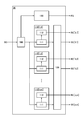
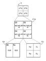
본 발명의 일 형태의 장치는 디코더, 구동 회로, 및 표시부를 포함한다. 구동 회로는 복수의 회로를 포함한다. 표시부는 복수의 표시 패널을 포함한다. 디코더는 표시부에 표시되는 화상에 대응하는 신호를 생성한다. 디코더는 각 표시 패널에서의 화상의 변화를 검출하고 각 표시 패널에서 화상의 재기록이 필요할지 여부를 판정한다. 회로는 화상의 재기록이 필요하다고 판정된 표시 패널에 신호를 출력한다. 회로는 화상의 재기록이 필요 없다고 판정된 표시 패널로의 신호의 출력을 정지한다.An apparatus of an aspect of the present invention includes a decoder, a driving circuit, and a display unit. The driving circuit includes a plurality of circuits. The display section includes a plurality of display panels. The decoder generates a signal corresponding to the image displayed on the display unit. The decoder detects a change in the image on each display panel and determines whether or not it is necessary to rewrite the image on each display panel. The circuit outputs a signal to the display panel determined to require rewriting of the image. The circuit stops outputting the signal to the display panel determined not to require rewriting of the image.
본 발명의 일 형태의 장치는 디코더, 구동 회로, 및 표시부를 포함한다. 구동 회로는 복수의 회로를 포함한다. 표시부는 복수의 표시 패널을 포함한다. 디코더는 표시부에 표시되는 화상에 대응하는 제 1 신호를 생성한다. 디코더는 각 표시 패널에서의 화상의 변화를 검출하고 각 표시 패널에서 화상의 재기록이 필요할지 여부를 판정한다. 회로는 화상의 재기록이 필요하다고 판정된 표시 패널에 제 1 신호를 출력한다. 회로는 화상의 재기록이 필요 없다고 판정된 표시 패널로의 제 1 신호의 출력을 정지한다. 디코더는 복수의 회로로부터 표시부로의 신호의 출력을 동기화시키는 제 2 신호를 생성한다.An apparatus of an aspect of the present invention includes a decoder, a driving circuit, and a display unit. The driving circuit includes a plurality of circuits. The display section includes a plurality of display panels. The decoder generates a first signal corresponding to an image displayed on the display unit. The decoder detects a change in the image on each display panel and determines whether or not it is necessary to rewrite the image on each display panel. The circuit outputs the first signal to the display panel determined to require rewriting of the image. The circuit stops outputting the first signal to the display panel determined to be unnecessary to rewrite the image. The decoder generates a second signal that synchronizes the output of the signal from the plurality of circuits to the display unit.
본 발명의 일 형태의 장치에서는, 디코더는 표시 패널에 표시되는 화상의 움직임 벡터의 값 및 표시 패널에 표시되는 화상의 프레임 간 예측의 예측 오차에 기초하여 판정을 수행하여도 좋다.In an apparatus of an aspect of the present invention, the decoder may perform determination based on a value of a motion vector of an image displayed on a display panel and a prediction error of inter-frame prediction of an image displayed on the display panel.
본 발명의 일 형태의 장치에서는, 표시 패널은 화소를 포함하여도 좋다. 화소는 트랜지스터 및 표시 소자를 포함하여도 좋다. 트랜지스터의 소스 및 드레인 중 한쪽을 배선과 전기적으로 접속하여도 좋다. 트랜지스터의 소스 및 드레인 중 다른 쪽을 표시 소자와 전기적으로 접속하여도 좋다. 배선은 화소에 표시되는 그레이레벨에 대응하는 전위를 전달하여도 좋다. 트랜지스터는 채널 형성 영역에 산화물 반도체를 포함하여도 좋다.In an apparatus of an aspect of the present invention, the display panel may include pixels. The pixel may include a transistor and a display element. One of the source and the drain of the transistor may be electrically connected to the wiring. And the other of the source and the drain of the transistor may be electrically connected to the display element. The wiring may transmit a potential corresponding to the gray level displayed on the pixel. The transistor may include an oxide semiconductor in the channel forming region.
본 발명의 일 형태의 장치에서는, 회로를 표시 패널의 내측에 제공하여도 좋다.본 발명의 일 형태의 텔레비전 시스템은 상술한 장치를 포함한다. 텔레비전 시스템은 방송 신호를 수신하여 비트스트림 데이터를 생성하고 비트스트림 데이터에 기초하여 화상을 표시한다.In an apparatus of an aspect of the present invention, a circuit may be provided inside the display panel. A television system of one form of the present invention includes the above-described apparatus. The television system receives the broadcast signal to generate bitstream data and displays the image based on the bitstream data.
본 발명의 일 형태의 전자 기기는 상술한 장치 또는 상술한 텔레비전 시스템과, 마이크로폰, 스피커, 조작 스위치, 또는 센서를 포함한다.An electronic apparatus of an embodiment of the present invention includes the above-described apparatus or the above-described television system, a microphone, a speaker, an operation switch, or a sensor.
본 발명의 일 형태는 신규 장치를 제공할 수 있다. 또는, 본 발명의 일 형태에 따르면, 소비전력이 낮은 장치를 제공할 수 있다. 본 발명의 일 형태에 따르면, 다용도의 장치를 제공할 수 있다.One aspect of the present invention can provide a novel apparatus. Alternatively, according to an aspect of the present invention, a device with low power consumption can be provided. According to one aspect of the present invention, a versatile apparatus can be provided.
또한, 이들 효과의 기재는 다른 효과의 존재를 방해하지 않는다. 본 발명의 일 형태는 반드시 이들 효과 모두를 가질 필요는 없다. 다른 효과는 명세서, 도면, 및 청구항 등의 기재로부터 명백해질 것이며 추출할 수 있는 것이다.In addition, the description of these effects does not preclude the presence of other effects. One form of the invention need not necessarily have all of these effects. Other effects will be apparent from and elucidated from the description of the specification, drawings, claims, and the like.
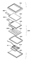
도 1은 장치의 구성예를 도시한 것이다.
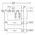
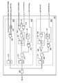
도 2는 디코더의 구성예를 나타내는 도면이다.
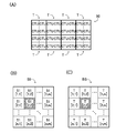
도 3은 CTU를 도시한 것이다.
도 4의 (A) 내지 (C)는 타일을 도시한 것이다.
도 5는 유닛의 구성예를 나타낸 것이다.
도 6은 신호 생성 회로의 구성예를 나타낸 것이다.
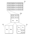
도 7은 CU의 분할을 도시한 것이다.
도 8은 판정 회로의 구성예를 도시한 것이다.
도 9는 신호 생성 회로의 구성예를 도시한 것이다.
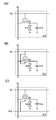
도 10의 (A) 내지 (C)는 표시 장치의 구성예를 도시한 것이다.
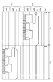
도 11은 타이밍 차트이다.
도 12의 (A) 내지 (C)는 화소의 구성예를 각각 도시한 것이다.
도 13의 (A) 내지 (C)는 화소의 구성예를 각각 도시한 것이다.
도 14의 (A) 내지 (C)는 회로의 구성예를 각각 도시한 것이다.
도 15의 (A) 내지 (F)는 회로의 구성예를 각각 도시한 것이다.
도 16의 (A) 및 (B)는 회로의 구성예를 각각 도시한 것이다.
도 17의 (A) 및 (B)는 회로의 구성예를 각각 도시한 것이다.
도 18은 방송 시스템의 예를 도시한 것이다.
도 19는 데이터 전송의 예를 도시한 것이다.
도 20은 응급 의료 시스템의 예를 도시한 것이다.
도 21의 (A) 내지 (D)는 수신 장치의 구성예를 각각 도시한 것이다.
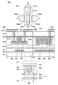
도 22의 (A1), (A2), (B1), (B2), (C1), 및 (C2)는 트랜지스터의 구성예를 도시한 것이다.
도 23의 (A1), (A2), (A3), (B1), 및 (B2)는 트랜지스터의 구성예를 도시한 것이다.
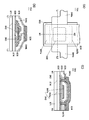
도 24의 (A1), (A2), (A3), (B1), (B2), (C1), 및 (C2)는 트랜지스터의 구성예를 도시한 것이다.
도 25의 (A) 내지 (C)는 트랜지스터의 구성예를 도시한 것이다.
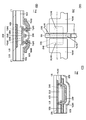
도 26의 (A) 내지 (C)는 트랜지스터의 구성예를 도시한 것이다.
도 27의 (A) 내지 (C)는 트랜지스터의 구성예를 도시한 것이다.
도 28의 (A) 및 (B)는 트랜지스터의 구성예를 도시한 것이다.
도 29의 (A) 및 (B)는 트랜지스터의 구성예를 도시한 것이다.
도 30의 (A) 내지 (C)는 트랜지스터의 구성예를 도시한 것이다.
도 31의 (A) 내지 (C)는 트랜지스터의 구성예를 도시한 것이다.
도 32의 (A) 내지 (C)는 트랜지스터의 구성예를 도시한 것이다.
도 33의 (A) 및 (B)는 에너지 밴드 다이어그램이다.
도 34의 (A) 내지 (C)는 표시 장치의 구성예를 도시한 것이다.
도 35의 (A) 및 (B)는 표시 장치의 구성예를 도시한 것이다.
도 36의 (A) 및 (B)는 장치의 구성예를 도시한 것이다.
도 37은 표시 모듈의 구성예를 도시한 것이다.
도 38의 (A) 내지 (F)는 전자 기기의 구성예를 각각 도시한 것이다.
도 39의 (A) 및 (B)는 트랜지스터의 동작예를 도시한 것이다.
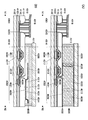
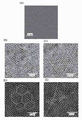
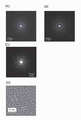
도 40의 (A) 내지 (E)는 XRD에 의한 CAAC-OS 및 단결정 산화물 반도체의 구조 분석, 및 CAAC-OS의 제한 시야 전자 회절 패턴을 나타낸 것이다.
도 41의 (A) 내지 (E)는 CAAC-OS의 단면 TEM 이미지 및 평면 TEM 이미지, 및 그 분석을 통하여 얻은 이미지이다.
도 42의 (A) 내지 (D)는 nc-OS의 전자 회절 패턴 및 단면 TEM 이미지를 나타낸 것이다.
도 43의 (A) 및 (B)는 a-like OS의 단면 TEM 이미지이다.
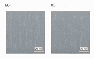
도 44는 전자 조사에 의하여 유발되는 In-Ga-Zn 산화물의 결정부에서의 변화를 나타낸 것이다.
도 45는 채널 형성 영역에 산화물 반도체를 포함하는 트랜지스터의 에너지 밴드를 나타내는 도면이다.1 shows a configuration example of an apparatus.
2 is a diagram showing a configuration example of a decoder.
Figure 3 shows a CTU.
4 (A) to 4 (C) show the tiles.
5 shows an example of the configuration of the unit.
6 shows an example of the configuration of the signal generating circuit.
Fig. 7 shows the division of the CU.
Fig. 8 shows a configuration example of the determination circuit.
Fig. 9 shows a configuration example of the signal generation circuit.
10A to 10C show a configuration example of a display device.
11 is a timing chart.
Figs. 12A to 12C each show an example of the configuration of a pixel.
Figs. 13A to 13C each show an example of the configuration of a pixel.
Figs. 14A to 14C each show an example of the configuration of a circuit. Fig.
Figs. 15A to 15F each show a configuration example of a circuit.
Figs. 16A and 16B each show an example of the configuration of a circuit.
17A and 17B each show an example of the configuration of a circuit.
18 shows an example of a broadcast system.
19 shows an example of data transmission.
20 shows an example of an emergency medical system.
Figs. 21A to 21D each show a configuration example of a reception apparatus. Fig.
(A1), (A2), (B1), (B2), (C1), and (C2) in FIG.
(A1), (A2), (A3), (B1), and (B2) in FIG. 23 show a configuration example of a transistor.
(A1), (A2), (A3), (B1), (B2), (C1), and (C2) in FIG.
25A to 25C show a configuration example of a transistor.
Figs. 26A to 26C show a configuration example of a transistor.
Figs. 27A to 27C show a configuration example of a transistor.
Figs. 28A and 28B show a configuration example of a transistor.
29A and 29B show an example of the configuration of a transistor.
Figs. 30A to 30C show a configuration example of a transistor.
Figs. 31A to 31C show a configuration example of a transistor.
32A to 32C show a configuration example of a transistor.
33 (A) and 33 (B) are energy band diagrams.
Figs. 34A to 34C show a configuration example of a display device. Fig.
Figs. 35A and 35B show a configuration example of a display device. Fig.
Figures 36 (A) and 36 (B) show examples of the configuration of the apparatus.
37 shows a configuration example of the display module.
38 (A) to (F) show an example of the configuration of an electronic apparatus, respectively.
Figs. 39A and 39B show operation examples of the transistors.
40 (A) to (E) show structural analysis of CAAC-OS and single crystal oxide semiconductor by XRD, and limited viewing electron diffraction pattern of CAAC-OS.
41 (A) to 41 (E) are cross-sectional TEM images and plane TEM images of CAAC-OS, and images obtained through the analysis.
42 (A) to 42 (D) show electron diffraction patterns of nc-OS and cross-sectional TEM images.
43 (A) and 43 (B) are cross-sectional TEM images of an a-like OS.
Fig. 44 shows the change in the crystal part of the In-Ga-Zn oxide caused by electron irradiation.
45 is a diagram showing an energy band of a transistor including an oxide semiconductor in a channel forming region.
본 발명의 실시형태에 대하여 첨부 도면을 참조하여 이하에서 자세히 설명한다. 또한, 본 발명은 이하의 설명에 한정되지 않고, 본 발명의 범위 및 취지에서 벗어남이 없이 형태 및 자세한 사항을 다양하게 변경할 수 있다는 것은 통상의 기술자에 의하여 용이하게 이해된다. 따라서, 본 발명은 이하의 실시형태의 기재에 한정하여 해석되어서는 안 된다.Embodiments of the present invention will be described in detail below with reference to the accompanying drawings. It is to be understood by those skilled in the art that the present invention is not limited to the following description, and that various changes in form and detail can be made without departing from the scope and spirit of the present invention. Therefore, the present invention should not be construed as being limited to description of the following embodiments.
본 발명의 일 형태는 장치, 텔레비전 시스템, 및 전자 기기에 더하여, 표시 장치, 기억 장치, 촬상 장치, 및 RF(Radio Frequency) 태그를 그 범주에 포함한다. 표시 장치는 액정 표시 장치, 유기 발광 소자로 대표되는 발광 소자가 각각 제공되는 화소를 갖는 발광 장치, 전자 종이, DMD(digital micromirror device), PDP(plasma display panel), 및 FED(field emission display) 등을 그 범주에 포함한다.An aspect of the present invention includes a display device, a storage device, an image pickup device, and an RF (Radio Frequency) tag in addition to the device, the television system, and the electronic device. A display device includes a liquid crystal display, a light emitting device having pixels each provided with a light emitting element typified by an organic light emitting element, an electronic paper, a digital micromirror device (DMD), a plasma display panel (PDP) Are included in the category.
또한, 본 명세서 등에서는, "X와 Y가 접속된다"라는 명시적인 기재는 X와 Y가 전기적으로 접속되는 것, X와 Y가 기능적으로 접속되는 것, 그리고 X와 Y가 직접 접속되는 것을 의미한다. 따라서, 소정의 접속 관계, 예를 들어, 도면 또는 문장에 나타낸 접속 관계에 한정되지 않고, 도면 또는 문장에는 다른 접속 관계가 포함된다. 여기서, X 및 Y는 각각 물체(예를 들어, 장치, 소자, 회로, 배선, 전극, 단자, 도전막, 또는 층)를 나타낸다.Also, in this specification and the like, an explicit description of " X and Y connected" means that X and Y are electrically connected, that X and Y are functionally connected, and that X and Y are directly connected do. Thus, the connection relationship shown in the figure or the sentence is not limited to the predetermined connection relationship, for example, the connection relationship shown in the drawings or the sentence, and the connection or the like includes other connection relations. Here, X and Y represent an object (e.g., an apparatus, an element, a circuit, a wiring, an electrode, a terminal, a conductive film, or a layer).
X와 Y가 직접 접속되는 경우의 예에는, X와 Y 사이의 전기적인 접속을 가능하게 하는 소자(예를 들어, 스위치, 트랜지스터, 용량 소자, 인덕터, 레지스터, 다이오드, 표시 소자, 발광 소자, 및 부하)가 X와 Y 사이에 접속되지 않는 경우, 및 X와 Y가 X와 Y 사이의 전기적인 접속을 가능하게 하는 소자를 개재(介在)하지 않고 접속되는 경우가 포함된다.For the case where X and Y are direct connection is, X and the electrical device that enables the connection (e.g., a switch, a transistor, a capacitor element, an inductor, a resistor, a diode, a display element, a light emitting device between the Y, and Load) is not connected between X and Y , and X and Y are connected without interposing an element that enables electrical connection between X and Y , as shown in FIG.
예를 들어, X와 Y가 전기적으로 접속되는 경우, X와 Y 사이에 전기적으로 접속시킬 수 있는 하나 이상의 소자(예를 들어, 스위치, 트랜지스터, 용량 소자, 인덕터, 레지스터, 다이오드, 표시 소자, 발광 소자, 또는 부하)를 X와 Y 사이에 접속시킬 수 있다. 또한, 스위치는 온 또는 오프가 되도록 제어된다. 즉, 스위치가 도통 또는 비도통이 되어(온 또는 오프가 되어) 전류를 흘릴지 여부를 결정한다. 또는, 스위치는 전류 경로를 선택하여 변환하는 기능을 갖는다. 또한, X와 Y가 전기적으로 접속되는 경우에는, X와 Y가 직접 접속되는 경우가 포함된다.For example, if X and Y are electrically connected to, one or more elements which can be electrically connected between X and Y (e.g., switch, transistor, capacitor element, an inductor, a resistor, a diode, a display element, the light emitting Element, or load) between X and Y can be connected. Also, the switch is controlled to be on or off. That is, it is determined whether or not the switch conducts or non-conducts (turns on or off) and flows a current. Alternatively, the switch has a function of selecting and converting the current path. When X and Y are electrically connected, the case where X and Y are directly connected is included.
예를 들어, X와 Y가 기능적으로 접속되는 경우, X와 Y 사이에 기능적으로 접속시킬 수 있는 회로(예를 들어, 인버터, NAND 회로, 또는 NOR 회로 등의 논리 회로; DA 변환 회로, AD 변환 회로, 또는 감마 보정 회로 등의 신호 변환 회로; 전원 회로(예를 들어, 스텝업 회로 또는 스텝다운 회로) 또는 신호의 전위 레벨을 변경하기 위한 레벨 시프터 회로 등의 전위 레벨 변환 회로; 전압원; 전류원; 스위칭 회로; 신호 진폭 또는 전류량 등을 증가시킬 수 있는 회로, 연산 증폭기, 차동 증폭 회로, 소스 폴로어 회로, 또는 버퍼 회로 등의 증폭 회로; 신호 생성 회로; 기억 회로; 및/또는 제어 회로)를 X와 Y 사이에 하나 이상 접속시킬 수 있다. 예를 들어, X와 Y 사이에 다른 회로가 개재되더라도, X로부터 출력된 신호가 Y로 전달되면 X와 Y는 기능적으로 접속된다. 또한, X와 Y가 기능적으로 접속되는 경우에는 X와 Y가 직접 접속되는 경우 및 X와 Y가 전기적으로 접속되는 경우가 포함된다.For example, when X and Y are functionally connected, a circuit that can be functionally connected between X and Y (for example, a logic circuit such as an inverter, a NAND circuit, or a NOR circuit, a DA conversion circuit, A power source circuit (e.g., a step-up circuit or a step-down circuit), or a level shifter circuit for changing a potential level of a signal, a voltage source circuit such as a voltage source, a current source, a switching circuit; circuit that can increase signal amplitude, the amount of current, such as an operational amplifier, a differential amplifier circuit, a source follower circuit, or an amplifier circuit such as a buffer circuit; signal generating circuit; memory circuit; and / or a control circuit), an X And Y can be connected. For example, even if another circuit is interposed between X and Y , if the signal output from X is transferred to Y , X and Y are functionally connected. Also, when X and Y are functionally connected, the case where X and Y are directly connected and the case where X and Y are electrically connected is included.
또한, 본 명세서 등에서, "X와 Y가 전기적으로 접속된다"라는 명시적인 기재는, X와 Y가 전기적으로 접속되는 것(즉, X와 Y가 다른 소자 또는 다른 회로를 개재하여 접속되는 경우), X와 Y가 기능적으로 접속되는 것(즉, X와 Y가 다른 회로를 개재하여 기능적으로 접속되는 경우), 그리고 X와 Y가 직접 접속되는 것(즉, X와 Y가 다른 소자 또는 다른 회로를 개재하지 않고 접속되는 경우)을 의미한다. 즉, 본 명세서 등에서, "X와 Y가 전기적으로 접속된다"라는 명시적인 기재는 "X와 Y가 접속된다"라는 기재와 같다.Further, in this specification and the like, an explicit description that " X and Y are electrically connected" is a description that X and Y are electrically connected (that is, when X and Y are connected via another element or another circuit) , Where X and Y are functionally connected (ie, when X and Y are functionally connected via different circuits), and X and Y are directly connected (ie, when X and Y are different devices or different circuits Quot; is connected without intervening between the terminals). That is, etc. As used herein, "X and Y are electrically connected to," that express the substrate is the same as the base material of "X and Y are connected."
도면을 참조하여 본 발명의 구조를 설명함에 있어서, 상이한 도면들의 같은 부분에는 같은 부호를 공통적으로 사용하는 경우가 있다.In describing the structure of the present invention with reference to the drawings, the same reference numerals are commonly used for the same parts in different drawings.
도면에서 독립된 구성요소들이 서로 전기적으로 접속되더라도, 하나의 구성요소가 복수의 구성요소의 기능을 갖는 경우가 있다. 예를 들어 배선의 일부가 전극으로서도 기능하는 경우, 하나의 도전막은 배선 및 전극으로서 기능한다. 따라서, 본 명세서에서 "전기적인 접속"은, 하나의 도전막이 복수의 구성요소의 기능을 갖는 경우를 그 범주에 포함한다.Although independent components are electrically connected to each other in the drawings, one component may function as a plurality of components. For example, when a part of the wiring also functions as an electrode, one conductive film functions as a wiring and an electrode. Thus, the term " electrical connection " in this specification includes the case where one conductive film has the function of a plurality of components.
(실시형태 1)(Embodiment 1)
본 실시형태에서는, 본 발명의 일 형태에 따른 장치에 대하여 설명한다.In this embodiment, an apparatus according to an aspect of the present invention will be described.
<장치의 구성예><Configuration Example of Device>
도 1은 장치(10)의 구성예를 도시한 것이다. 방송 신호를 수신하고 표시부에 영상을 표시하는 기능을 갖는 텔레비전 시스템에 장치(10)를 사용할 수 있다. 장치(10)는 프런트 엔드부(20), 디코더(30), 구동 회로(40), 및 표시부(50)를 포함한다.Fig. 1 shows a configuration example of the
8K 방송의 부호화 규격으로서는 새로운 규격인 H.265|MPEG-H high efficiency video coding(이하, HEVC라고 함)이 채용되어 있다. 장치(10)를 HEVC의 텔레비전 시스템에 사용할 수 있다.H.265 | MPEG-H high efficiency video coding (hereinafter referred to as " HEVC ") is adopted as a coding standard for 8K broadcasting. The
프런트 엔드부(20)는 방송 신호(신호 BS)를 수신하고 신호 처리를 수행하는 기능을 갖는 회로이다. 구체적으로, 프런트 엔드부(20)는 수신한 신호 BS의 복조 및 디지털 아날로그 변환 등을 수행함으로써 비트스트림 데이터(신호 BD)에 대응하는 신호를 생성하는 기능을 갖는다. 또한, 프런트 엔드부(20)는 에러를 정정하는 기능을 가져도 좋다.The
디코더(30)는 신호 BD를 복호함으로써, 표시부(50)에 표시되는 화상에 대응하는 신호(신호 SS)를 생성하는 기능을 갖는다. 예를 들어, 디코더(30)는 엔트로피 복호, 역양자화, IDCT(역이산 코사인 변환) 또는 IDST(역이산 사인 변환) 등의 역직교 변환, 프레임 내 예측, 및 프레임 간 예측 등을 수행하는 기능을 갖는다. 신호 BS가 HEVC로 부호화되는 경우, CABAC(context adaptive binary arithmetic coding) 복호가 디코더(30)에서 수행된다. 디코더(30)에서 생성된 신호 SS는 구동 회로(40)에 출력된다.The
구동 회로(40)는 표시부(50)에서의 화상의 표시를 제어하는 기능을 갖는다. 구체적으로, 구동 회로(40)는 표시부(50)의 특정한 영역을 선택하기 위한 신호(신호 GS) 및 신호 GS에 의하여 선택된 영역에 공급되는 신호 SS를 출력하는 기능을 갖는다. 구동 회로(40)에서는 화상 처리(예를 들어 감마 처리) 또는 디지털 아날로그 변환 등을 신호 SS에 수행하여도 좋다. 또한, 구동 회로(40)를 표시부(50)에 제공할 수 있다.The driving
표시부(50)는 구동 회로(40)로부터 입력되는 신호 GS 및 SS에 기초하여 화상을 표시하는 기능을 갖는다. 정지 화상 및 동영상 중 어느 쪽을 표시부(50)에 표시하여도 좋다. 예를 들어, 표시부(50)는 액정 표시 장치 또는 발광 표시 장치를 포함할 수 있다.The
여기서, 표시부(50)는 복수의 표시 패널(51)을 포함한다. 도 1에는, n행 m열(n 및 m은 자연수)의 매트릭스로 배열된 표시 패널(51)(표시 패널(51[1,1] 내지 51[n,m]))이 표시부(50)에 제공되는 구성예를 나타내었다. 표시 패널(51)을 독립적으로 제어할 수 있다.Here, the
표시부(50)는 복수의 표시 패널(51)을 사용하여 하나의 화상을 표시할 수 있다. 따라서, 표시부(50)의 화상 표시 영역을 확대할 수 있다. 표시부(50)는 복수의 표시 패널(51)을 포함하기 때문에, 각 표시 패널(51)을 크게 할 필요가 없다. 따라서, 표시 패널의 제작 장치를 대형화할 필요가 없으므로, 공간 절약화를 달성할 수 있다. 또한, 표시 패널(51)의 제작에는 중소형 표시 패널의 제작 장치를 사용할 수 있기 때문에, 대형 표시 장치를 위하여 다른 제작 장치를 준비할 필요가 없으므로, 제작 비용이 저감된다. 또한, 표시 패널의 대형화에 따른 수율의 저하를 억제할 수 있다.The
표시부(50)는 n×m의 표시 패널(51)을 사용하여 하나의 화상을 표시할 수 있지만, 본 발명의 일 형태는 이에 한정되지 않는다. 예를 들어, 표시부(50)를 분할하여 복수의 화상을 표시하여도 좋고, 또는 n×m의 표시 패널(51)에 다른 화상을 표시하여도 좋다.
여기서는, 표시부(50)에 화상을 표시할 때, 현재 프레임과 전(前) 프레임 사이에서 화상의 변화가 없거나, 또는 화상의 변화가 소정의 값 이하인 표시 패널(51)을 포함하는 경우가 있다. 표시 패널(51) 등에서는 화상의 재기록이 수행되지 않고, 전 프레임에서 표시된 화상을 저장하기 위한 구동이 수행될 수 있다. 이와 같이 하여, 화상의 재기록과 관련된 소비전력을 저감할 수 있다.Here, there is a case in which there is no image change between the current frame and the previous frame when the image is displayed on the
본 발명의 일 형태에서는, 디코더(30)를 사용함으로써, 화상의 변화가 없거나 화상의 변화가 소정의 값 이하인 표시 패널(51)에서의 화상의 재기록 동작을 정지시킨다. 구체적으로, 디코더(30)는 신호 BD에 기초한 각 표시 패널(51)의 화상의 재기록 여부를 판정하고, 그 여부에 대응하는 신호(신호 RC)를 구동 회로(40)에 출력하는 기능을 갖는다. 구동 회로(40)는, 신호 RC에 따라 표시 패널(51)에 표시되는 화상을 재기록 또는 저장한다.In one aspect of the present invention, by using the
구동 회로(40)는 표시 패널(51)과 같은 수의 회로(41)를 포함한다. 도 1에서는, 표시부(50)는 n×m의 표시 패널(51)을 포함하기 때문에 구동 회로(40)는 n×m의 회로(41)(회로(41[1,1] 내지 41[n,m]))를 포함한다. 그리고, 회로(41)는 각 표시 패널(51)에서 화상의 표시를 제어한다. 구체적으로는, 신호 SS[i,j] 및 신호 RC[i,j]를 디코더(30)로부터 회로(41[i,j])(i는 1 이상 n 이하의 정수(整數), 및 j는 1 이상 m 이하의 정수)에 출력한다. 신호 GS[i,j] 및 신호 SS[i,j]를 회로(41[i,j])로부터 표시 패널(51[i,j])에 입력한다.The driving
회로(41)로부터 표시 패널(51)로의 신호 GS 및 SS의 출력은, 디코더(30)로부터 회로(41)에 입력되는 신호 RC에 기초하여 제어된다. 구체적으로는, 디코더(30)에 의하여 화상의 재기록이 필요하다고 판정되는 표시 패널(51)에 대응하는 회로(41)는, 신호 GS 및 SS를 표시 패널(51)에 출력하고 표시 패널(51)에 표시되는 화상을 재기록한다. 한편, 화상의 재기록이 필요 없다고 판정되는 표시 패널(51)에 대응하는 회로(41)는, 신호 GS 및 SS를 출력하지 않아, 표시 패널(51)에 표시되는 화상을 재기록하지 않는다. 따라서, 신호 GS 및 SS를 출력하지 않는 회로(41)의 동작을 정지할 수 있으므로, 소비전력을 저감할 수 있다.The outputs of the signals GS and SS from the
화상의 재기록이 필요 없다고 판정되는 표시 패널(51)은, 예를 들어 변화하지 않는 배경 화상 등을 표시하는 표시 패널(51), 정지 화상을 표시하는 표시 패널(51), 또는 화상의 변화가 소정의 값 이하인 표시 패널(51)이어도 좋다.The
도 1에서는 회로(41)가 표시 패널(51)의 외부에 제공되지만, 회로(41)는 표시 패널(51) 내에 제공되어도 좋다. 신호 GS 및 SS를 저마다의 회로에 의하여 생성하여도 좋다.In Fig. 1, the
디코더(30)는 구동 회로(40)의 동작을 제어하기 위한 동기 신호(신호 FS)를 생성하는 기능을 갖는다. 디코더(30)로부터 회로(41[1,1] 내지 41[n,m])로 신호 FS를 입력하는 경우, 회로(41[1,1] 내지 41[n,m])로부터의 신호 GS 및 SS의 출력은 동기화된다. 따라서, 구동 회로(40)로부터 표시부(50)로의 신호 출력의 타이밍을 맞춤으로써 복수의 표시 패널(51)을 사용하는 화상을 표시부(50)에 표시할 수 있다.The
상술한 바와 같이, 본 발명의 일 형태에 따르면 화상의 재기록을 특정한 표시 패널(51)에서 생략할 수 있기 때문에 소비전력을 저감할 수 있다. 회로(41) 및 표시 패널(51)의 구체적인 구성예 및 동작예에 대해서는 실시형태 2에서 설명한다.As described above, according to the embodiment of the present invention, since the rewriting of the image can be omitted in the
<디코더의 구성예><Configuration example of decoder>
디코더(30)의 구체적인 예를 도 2에 나타내었다. 디코더(30)는 식별 회로(100), 복수의 신호 생성 회로(110), 루프 필터(120), 및 신호 생성 회로(130)를 포함한다.A concrete example of the
식별 회로(100)는 프런트 엔드부(20)로부터 입력되는 신호 BD를 분류하고 신호 생성 회로(110)에 출력하는 기능을 갖는다. 신호 BD는 표시 패널(51[1,1] 내지 51[n,m])의 화상 데이터를 포함한다. 그러므로, 식별 회로(100)는 어느 표시 패널(51)이 신호 BD에 포함되는 화상 데이터에 대응하는지를 판정하고, 표시 패널(51)에 대응하는 신호 생성 회로(110)에 화상 데이터를 출력한다. 도 2에서는, 표시 패널(51[1,1] 내지 51[n,m])에 대응하는 신호 생성 회로(110[1,1] 내지 110[n,m])를 제공하고, 신호 BD에 포함되는 화상 데이터를 n×m로 분할한다.The
식별 회로(100)는, 하나의 프레임의 화상 데이터가 신호 BD로서 입력될 때마다 신호 생성 회로(130)에 소정의 신호를 출력하는 기능을 갖는다.The
신호 생성 회로(110)는 디코더 회로(111) 및 판정 회로(112)를 포함한다. 디코더 회로(111)는 식별 회로(100)로부터 입력되는 화상 데이터를 복호하고 표시 패널(51)에 표시되는 화상에 대응하는 신호를 생성한다. 디코더 회로(111)는 엔트로피 복호, 역양자화, 역직교 변환, 프레임 내 예측, 또는 프레임 간 예측 등을 수행하는 기능을 갖는다. 디코더 회로(111)에서 생성되는 신호를 루프 필터(120)를 통하여 회로(41)에 출력한다.The
루프 필터(120)는 디코더 회로(111)에서 생성되는 신호에 여과 조작을 수행하는 기능을 갖고, 그것을 신호 SS로서 회로(41)에 출력한다. 따라서, 신호 SS에 포함되는 노이즈를 저감할 수 있다.The
판정 회로(112)는 디코더 회로(111)에서 복호된 신호에 기초하여, 표시 패널(51)에서 화상을 재기록할지 여부를 판정하는 기능을 갖는다. 구체적으로는, 현재 프레임과 전 프레임 사이의 화상의 변화를 각 표시 패널마다 검출함으로써, 화상의 재기록 여부를 각 표시 패널에 의하여 판정하고 판정 결과에 기초한 신호를 신호 RC로서 회로(41)에 출력한다.The
판정 회로(112)가 화상의 재기록이 필요하다고 판정하는 경우, 화상의 재기록이 필요한 경우에 대응하는 신호 RC를 판정 회로(112)로부터 회로(41)에 출력한다. 그리고, 회로(41)로부터 표시 패널(51)에 신호 GS 및 SS를 공급함으로써 표시 패널(51)에서 화상의 재기록이 수행된다. 한편, 판정 회로(112)가 화상의 재기록이 필요 없다고 판정하는 경우, 화상의 재기록이 필요 없는 경우에 대응하는 신호 RC를 판정 회로(112)로부터 회로(41)에 출력한다. 그리고, 회로(41)로부터 표시 패널(51)로의 신호 GS 및 SS의 공급이 정지됨으로써, 표시 패널(51)에서 화상의 재기록이 수행되지 않는다. 이러한 식으로, 화상을 재기록할지 여부를 각 표시 패널(51)마다 제어하여 소비전력을 저감할 수 있다.When the
판정 회로(112)에서의 신호 RC의 생성을 디코더 회로(111)에서의 복호 처리와 평행하여 수행할 수 있다. 그러므로 디코더(30)의 처리 속도를 향상시킬 수 있다. 또한, 판정 회로(112)의 구체적인 구성예에 대해서는 나중에 설명한다.The generation of the signal RC in the
신호 생성 회로(110[1,1] 내지 110[n,m])는 독립적으로 처리를 수행할 수 있다. 따라서, 신호 SS를 고속으로 생성할 수 있어 디코더(30)의 처리 속도를 향상시킬 수 있다. 또한, 사용자에 의하여 구성을 적절히 변경할 수 있는 장치(PLD: programmable logic device)를 신호 생성 회로(110)로서 사용할 수 있다. PLD의 예에는 SPLD(simple programmable logic device), CPLD(complex programmable logic device), 및 FPGA(field programmable gate array)가 포함된다.The signal generating circuits 110 [1, 1] to 110 [ n , m ] can independently perform processing. Therefore, the signal SS can be generated at a high speed, and the processing speed of the
신호 생성 회로(130)는 프레임 기간마다 식별 회로(100)로부터 입력되는 신호에 기초하여 신호 FS를 생성하고, 복수의 회로(41)에 신호 FS를 출력하는 기능을 갖는다. 복수의 회로(41)는 신호 FS에 기초하여 표시 패널(51)에 신호 GS 및 SS를 출력한다. 따라서, 복수의 회로(41)로부터 표시부(50)에 신호를 출력하는 타이밍을 제어함으로써, 복수의 표시 패널(51)에 표시되는 화상을 동기화할 수 있다. 또한, 신호 생성 회로(130)의 구체적인 구성예에 대해서는 나중에 설명한다.The
<장치의 동작예>≪ Example of operation of the device &
다음으로, 도 1에 나타낸 장치(10)의 동작예에 대하여 설명한다. 여기서는 예로서, 외부로부터 입력되는 신호 BS가 HEVC에 따른 방송 신호이고, 이 방송 신호에 기초하여 표시부(50)에 화상이 표시되는 경우의 동작에 대하여 설명한다.Next, an operation example of the
먼저, 신호 BS를 프런트 엔드부(20)에 입력한다. 신호 BS를 HEVC에 의하여 부호화한다.First, the signal BS is input to the
여기서는, 기본적인 요소로서 CTU(coding tree unit)를 사용하여 HEVC의 신호 처리를 수행한다. 도 3은 표시부(50)에 표시되는 화상 데이터가 CTU의 그룹을 포함하는 상태를 나타내는 개략도이다.Here, signal processing of the HEVC is performed using a coding tree unit (CTU) as a basic element. 3 is a schematic diagram showing a state in which the image data displayed on the
각 CTU는 복수의 블록의 CU(coding unit)를 포함한다. CU는 부호화와 복호를 수행하는 단위인 블록이다. 도 3에 도시된 바와 같이, CTU는 상이한 블록 크기를 갖는 CU의 그룹을 포함할 수 있다.Each CTU includes a plurality of blocks of CUs (coding units). The CU is a block that performs encoding and decoding. As shown in FIG. 3, a CTU may include a group of CUs having different block sizes.
CU를 분할하여 PU(prediction unit)를 형성한다. PU는 예측을 수행하기 위한 단위인 블록이다. PU의 분할을 수행할지 여부 또는 PU의 분할 수를 처리 내용에 따라 결정한다.The CU is divided to form a prediction unit (PU). PU is a block that is a unit for performing prediction. Whether to perform the division of the PU or the number of divisions of the PU is determined according to the processing contents.
CU를 분할하여 TU(transformation unit)를 형성한다. CU는 직교 변환, 역직교 변환, 양자화, 및 역양자화를 수행하기 위한 단위인 블록이다. TU의 분할을 수행할지 여부 또는 TU의 분할 수를 처리 내용에 따라 결정한다.CU is divided to form a transformation unit (TU). The CU is a block that is a unit for performing orthogonal transformation, inverse orthogonal transformation, quantization, and inverse quantization. Whether to perform the division of the TU or the number of divisions of the TU is determined according to the contents of the processing.
복수의 CTU를 포함하는 타일이라고 불리는 각 블록에서, 부호화 및 복호를 독립적으로 수행할 수 있다. 도 4의 (A)는, 표시부(50)에 표시되는 화상 데이터가 복수의 타일 T로 분할되는 상태를 나타내는 개략도이다. 화상 데이터는 복수의 타일 T를 포함하고, 각 타일 T마다 부호화 및 복호가 수행된다.In each block called a tile including a plurality of CTUs, encoding and decoding can be performed independently. 4A is a schematic diagram showing a state in which image data displayed on the
도 4의 (B)에 도시된 바와 같이, 표시부(50)는 복수의 표시 패널(51[1,1] 내지 51[n,m])의 그룹을 포함한다. 본 발명의 일 형태에 따르면, 신호 BS에 포함되는 하나의 프레임의 화상 데이터를 도 4의 (C)에 도시된 바와 같이, n×m의 타일 T(타일 T[1,1] 내지 T[n,m])로 분할하고 처리한다. 이에 의하여, 하나의 타일 T가 하나의 표시 패널(51)에 대응하고, 부호화 및 복호를 각 표시 패널(51)마다 독립적으로 수행할 수 있다. 예를 들어, 도 4의 (B) 및 (C)에 도시된 바와 같이, 타일 T[2,2]의 데이터를 표시 패널(51[2,2])의 화상 데이터로서 사용할 수 있다.As shown in Fig. 4 (B), the
상술한 바와 같이, n×m의 타일 T로 분할되고 각 타일 T마다 부호화된 신호 BS를 프런트 엔드부(20)에 입력하는 경우, 프런트 엔드부(20)는 신호 BS의 복조, 디지털 아날로그 변환, 및 에러 정정을 수행하고, 비트스트림 데이터를 생성한다. 비트스트림 데이터를 신호 BD로서 디코더(30)에 입력한다.As described above, when the signal BS divided into n × m tiles T and encoded for each tile T is input to the
디코더(30)에 입력되는 신호 BD의 구성예를 도 5에 나타내었다. 신호 BD는 복수의 AU(access unit)를 포함한다. AU는 표시부(50)에 표시되는 화상의 하나의 프레임의 데이터를 포함한다.An example of the configuration of the signal BD input to the
AU는 복수의 유닛을 포함한다. 구체적으로, AU는 AU의 구분 문자를 포함하는 AUD(access unit delimiter), 표시부(50)에 표시되는 모든 프레임의 화상에 대한 설정 정보를 포함하는 VPS(video parameter set), 특정한 시퀀스에 포함되는 복수의 프레임에 대한 설정 정보를 포함하는 SPS(sequence parameter set), 각 프레임의 설정 정보를 포함하는 PPS(picture parameter set), 추가 정보의 접두사를 포함하는 PREFIX_SEI(supplemental enhancement information), 하나의 프레임의 화상 데이터를 포함하는 VCL(video coding layer), 추가 정보의 접미사를 포함하는 SUFFIX_SEI, 및 일정한 값으로 AU의 길이를 유지하기 위한 더미 데이터를 포함하는 FD(filler data) 등을 포함한다. 각 AU에서 FD의 길이를 VCL의 길이에 따라 조정함으로써, 신호 BS에 포함되는 복수의 AU의 길이를 동등하게 할 수 있다.The AU includes a plurality of units. Specifically, the AU includes an access unit delimiter (AUD) including the delimiter character of the AU, a VPS (video parameter set) including setting information for all frames of the image displayed on the
VCL는 n×m의 타일 T로 분할된 하나의 프레임의 화상 데이터를 포함한다. 또한, PPS는 타일 분할 정보(VCL에 포함되는 각 화상 데이터가 어느 타일에 속하는지에 대한 정보)를 포함한다. SPS는 프레임 간 예측의 참조 프레임에 대한 정보를 포함한다.The VCL includes image data of one frame divided into n占m tiles T. In addition, the PPS includes tile division information (information on which tile each image data included in the VCL belongs). The SPS contains information about the reference frame of the interframe prediction.
상술한 유닛을 포함하는 비트스트림 데이터를 신호 BD로서 식별 회로(100)에 입력한다(도 2 참조).The bit stream data including the above-mentioned unit is input to the
신호 BD를 식별 회로(100)에 입력하는 경우, 식별 회로(100)는 PPS에 포함되는 타일 분할 정보를 복호하고 VCL에 포함되는 화상 데이터를 복수의 신호 생성 회로(110)로 분류한다. 식별 회로(100)는, SPS에 포함되는 참조 프레임에 대한 정보를 복호하여 프레임 간 예측을 수행할지 여부를 판정한다. 식별 회로(100)가 AU에 포함되는 AUD를 인식할 때, 식별 회로(100)는 신호 생성 회로(130)에 신호를 출력한다. AU의 길이는 일정하기 때문에, 상기 신호가 프레임마다 일정한 간격으로 출력된다.When the signal BD is input to the
신호 생성 회로(110)는 식별 회로(100)로부터 입력된 신호에 기초하여 신호를 생성한다. 도 2에 나타낸 신호 생성 회로(110)의 더 구체적인 구성예는 도 6에 나타내었다. 도 6의 신호 생성 회로(110)는 HEVC에 따른 비트스트림 데이터를 복호할 수 있다. 여기서는 신호 생성 회로(110[1,1])의 구성예를 나타내지만, 이와 비슷한 구성을 신호 생성 회로(110[1,2] 내지 110[n,m])에 적용할 수 있다.The
도 6에 도시된 신호 생성 회로(110)는 디코더 회로(200), 변환 회로(210), 가산 회로(220), 프레임 내 예측 회로(230), 기억 회로(240), 프레임 간 예측 회로(250), 기억 회로(260), 및 판정 회로(112)를 포함한다.6 includes a
VCL에 포함되는 화상 데이터는 표시 패널(51[1,1] 내지 51[n,m])에 표시되는 화상 데이터에 대응하는 n×m의 신호(신호 vcl[1,1] 내지 vcl[n,m]로 표시함)로 분할된다. 신호 vcl[1,1] 내지 vcl[n,m]은 각 신호 생성 회로(110)에 포함되는 디코더 회로(200)에 입력된다. 또한, PPS에 포함되는 타일 분할 정보에 기초하여 화상 데이터를 분할한다.Image data includes a display panel (51 [1, 1] to 51 [n, m]) n × m signals (signal vcl [1,1] to vcl corresponding to the image data displayed on included in the VCL [n, m ]. The signals vcl [1,1] to vcl [ n , m ] are input to the
디코더 회로(200)는 식별 회로(100)로부터 입력되는 신호 vcl에 대한 CABAC 복호를 수행하는 기능을 갖는다. 디코더 회로(200)에 의하여 복호된 신호를 변환 회로(210)에 출력한다.The
변환 회로(210)는 디코더 회로(200)로부터 입력되는 신호에 대한 역양자화 및 역변환을 수행하는 기능을 갖는다. 변환 회로(210)에서 역양자화 및 역변환이 실시된 신호를 가산 회로(220)에 출력한다. 역양자화 및 역변환을 다른 회로에서 수행하여도 좋다.The
프레임 내 예측 또는 프레임 간 예측을 수행할 때, 가산 회로(220)는 변환 회로(210)에서 역양자화 및 역변환을 실시한 신호와 참조 데이터를 합함으로써, 표시 패널(51)에 표시되는 화상에 대응하는 신호를 생성하는 기능을 갖는다. 가산 회로(220)에서 생성된 신호는 루프 필터(120)에서 여과 연산이 실시되고 나서 신호 SS로서 회로(41)(도시되지 않음)에 출력된다.When the intra-frame prediction or the inter-frame prediction is performed, the
프레임 내 예측을 수행하는 경우, 프레임 내 예측 회로(230)는 기억 회로(240)로부터 참조 데이터를 판독하고 가산 회로(220)에 참조 데이터를 출력한다. 그리고, 역양자화 및 역변환이 실시된 신호와 참조 데이터를 가산 회로(220)에서 합하여 루프 필터(120)에 입력함으로써 신호 SS를 생성한다.When intra-frame prediction is performed, the
프레임 간 예측을 수행하는 경우, 프레임 간 예측 회로(250)는 기억 회로(260)로부터 참조 데이터를 판독하고 가산 회로(220)에 참조 데이터를 출력한다. 그리고 역양자화 및 역변환이 실시된 신호와 참조 데이터를 가산 회로(220)에서 합하여 루프 필터(120)에 입력함으로써 신호 SS를 생성한다.When performing inter-frame prediction, the
루프 필터(120)로부터 출력된 신호 SS를 새로운 참조 데이터로서 기억 회로(240 또는 260)에 저장한다. 프레임 내 예측 또는 프레임 간 예측을 다음 프레임에서 수행하는 경우, 상기 참조 데이터를 사용할 수 있다.And stores the signal SS output from the
디코더 회로(200)에서 복호된 화상 데이터를 판정 회로(112)에도 출력한다. 그리고 표시 패널(51)에 표시되는 화상의 재기록 여부를 판정 회로(112)에서 판정한다.And outputs decoded image data from the
구체적으로는, 먼저 하나의 타일 T에 포함되는 화상 데이터를 디코더 회로(200)에서 복호한다. 하나의 타일 T에 포함되는 화상 데이터는 하나의 표시 패널(51)의 하나의 프레임의 화상 데이터에 상당한다. 여기서, 도 7에 도시된 바와 같이, 타일 T는 복수의 CTU를 포함하고 CTU는 복수의 CU를 포함한다. CU는 PU 또는 TU를 포함할 수 있다. 타일 T에 포함되는 모든 PU의 움직임 벡터의 값을 판정하기 위한 제 1 판정 및 타일 T에 포함되는 모든 CU에서 TU를 분할할지 여부를 판정하기 위한 제 2 판정을 수행함으로써, 전 프레임을 기준으로서 사용하여 화상의 재기록 여부를 판정한다.Specifically, the
제 1 판정은 PU의 움직임 벡터가 (0,0)일지 여부를 판정함으로써 수행된다. 타일 T에 포함되는 모든 PU의 움직임 벡터가 (0,0)인 경우, 현재 프레임에 평행 이동의 성분이 없는 것을 의미한다. 제 2 판정은, CU에 포함되는 TU의 분할에 대한 정보(rqt_root_cbf)를 판독하고, CU가 TU로 분할되어 있는지 여부를 판정함으로써 수행된다. rqt_root_cbf=0인 경우, CU에 TU 트리 구조가 없고, 프레임 간 예측의 예측 오차가 없는 것을 의미한다. 따라서, 타일 T에 포함되는 모든 PU의 움직임 벡터가 (0,0)이고 타일 T에 포함되는 모든 CU에서 rqt_root_cbf=0인 경우, 전 프레임과 현재 프레임 사이에서 표시 패널(51)에 표시되는 화상의 변화가 없는 것을 의미한다. 여기서 판정 회로(112)는, 표시 패널(51)의 화상의 재기록은 필요 없다고 판정하고 화상의 재기록이 필요 없는 것을 나타내는 신호 RC를 회로(41)에 출력한다.The first determination is performed by determining whether the motion vector of the PU is (0, 0). When the motion vectors of all PUs included in the tile T are (0, 0), it means that there is no parallel movement component in the current frame. The second determination is performed by reading the information (rqt_root_cbf) about the division of the TU included in the CU and determining whether or not the CU is divided into TUs. When rqt_root_cbf = 0, it means that there is no TU tree structure in the CU, and there is no prediction error of the interframe prediction. Therefore, when the motion vectors of all the PUs included in the tile T are (0, 0) and rqt_root_cbf = 0 in all the CUs included in the tile T, the image displayed on the
한편, 움직임 벡터가 (0,0) 이외의 적어도 하나의 PU를 타일 T가 포함하는 경우 또는 rqt_root_cbf≠0인 적어도 하나의 CU를 타일 T가 포함하는 경우에는, 전 프레임과 현재 프레임 사이에서 표시 패널(51)에 표시되는 화상의 변화가 있는 것을 의미한다. 여기서 판정 회로(112)는, 표시 패널(51)의 화상의 재기록이 필요하다고 판정하고, 화상의 재기록이 필요한 것을 나타내는 신호 RC를 회로(41)에 출력한다.On the other hand, when the tile T contains at least one PU other than the motion vector (0, 0) or when the tile T includes at least one CU having rqt_root_cbf? 0, Quot; means that there is a change in the image displayed on the
여기서는, 타일 T에 포함되는 PU의 모든 움직임 벡터가 (0,0)이고 타일 T에 포함되는 모든 CU에서 rqt_root_cbf=0인 경우, 화상의 재기록은 필요 없다고 가정되지만, 화상의 재기록 여부를 판정하기 위한 기준은 적절히 설정할 수 있다. 예를 들어, 움직임 벡터가 소정의 값 이하인 경우 또는 rqt_root_cbf≠0의 PU의 수가 소정의 수 이하인 경우에는, 화상의 재기록을 필요 없는 것으로 할 수 있다.Here, when all the motion vectors of the PU included in the tile T are (0, 0) and rqt_root_cbf = 0 in all the CUs included in the tile T, it is assumed that the rewriting of the image is not necessary. However, The criteria can be set appropriately. For example, when the motion vector is equal to or less than a predetermined value or when the number of PUs with rqt_root_cbf? 0 is equal to or less than a predetermined number, rewriting of the image can be made unnecessary.
그리고 회로(41)(도 1에 도시됨)는 디코더(30)로부터 입력된 신호 RC에 기초하여 표시 패널(51)로의 신호 GS 및 SS의 출력을 제어한다. 화상의 재기록이 필요한 경우, 신호 GS 및 SS를 표시 패널(51)에 출력한다. 화상의 재기록이 필요 없는 경우, 표시 패널(51)로의 신호 GS 및 SS의 출력을 정지한다. 이에 의하여, 화상의 재기록 횟수를 줄여 구동 회로(40) 및 표시부(50)의 소비전력을 저감할 수 있다.1) controls the output of the signals GS and SS to the
신호 생성 회로(130)는 신호 BD에 기초하여 동기 신호(신호 FS)를 생성하고 회로(41[1,1] 내지 41[n,m])에 신호 FS를 출력한다. 회로(41[1,1] 내지 41[n,m])로부터 신호가 출력되는 타이밍은 신호 FS에 따라 제어된다.The
<판정 회로의 구성예><Configuration Example of Judgment Circuit>
도 8은 판정 회로(112)의 구체적인 구성예를 나타낸 것이다. 판정 회로(112)는 회로(300), 회로(310), 회로(320), 및 AND(330)를 포함한다.Fig. 8 shows a specific configuration example of the
도 8에서, 신호 CUcount_max는 타일 T에 포함되는 CU의 최대 수를 나타내는 신호이다. 신호 rqt_root_cbf는 CU에 TU 트리 구조가 존재할지 여부를 나타내는 신호이다. TU 트리 구조가 존재하는 경우, 신호의 값은 "1"이다. TU 트리 구조가 존재하지 않는 경우, 신호의 값은 "0"이다. 신호 PUcount_max는 타일 T에 포함되는 PU의 최대 수를 나타내는 신호이다. 신호 motionvector_x는 PU의 움직임 벡터의 x 성분을 나타내는 신호이다. 신호 motionvector_y는 PU의 움직임 벡터의 y 성분을 나타내는 신호이다. 신호 Current_POC는 현재 프레임의 번호를 나타내는 신호이다. 신호 Reference_POC는 프레임 간 예측의 기준인 프레임의 번호를 나타내는 신호이다. 신호 rqt_root_cbf는 HEVC에 따라 입력되는 신호이다.8, the signal CUcount_max is a signal indicating the maximum number of CUs included in the tile T. The signal rqt_root_cbf is a signal indicating whether or not a TU tree structure exists in the CU. If there is a TU tree structure, the value of the signal is " 1 ". If the TU tree structure does not exist, the value of the signal is " 0 ". The signal PUcount_max is a signal indicating the maximum number of PUs included in the tile T. Motionvector_ signal x is a signal that represents the x component of the motion vector of the PU. Motionvector_ signal y is a signal representative of the y component of the motion vector of the PU. The signal Current_POC is a signal indicating the number of the current frame. The signal Reference_POC is a signal indicating the number of a frame as a reference of inter-frame prediction. The signal rqt_root_cbf is a signal input according to HEVC.
회로(300)는 타일 T에 TU 트리 구조를 갖는 CU가 있는지 여부를 판정하는 기능을 갖는다. 회로(300)는 카운터(301), XNOR(302), OR(303), 플립플롭(FF)(304), 인버터(305), AND(306), 및 FF(307)를 포함한다.The
회로(300)의 동작예에 대하여 설명한다. 카운터(301)는 클록 신호 clk에 따라 카운트업하고, CU 번호에 대응하는 신호를 카운터(301)로부터 출력한다. 카운터(301)로부터 출력되는 CU 번호에 대응하는 CU의 신호 rqt_root_cbf를 OR(303)에 순차적으로 입력한다. OR(303)의 출력은 FF(304)에 저장된다. FF(304)의 출력은 OR(303)에 입력된다.An operation example of the
여기서는, 초기 상태에서, 데이터 "0"이 FF(304)에 저장된다. 그러므로, 처음에 입력된 신호 rqt_root_cbf가 "0"인 경우, OR(303)의 출력은 "0"이 되어 데이터 "0"이 FF(304)에 저장된다. 그리고, OR(303)에 입력되는 신호 rqt_root_cbf가 "0"인 한, OR(303)의 출력은 "0"이 되어 FF(304)는 이에 데이터 "0"이 저장된 상태로 유지된다. 한편, 신호 rqt_root_cbf가 "1"인 경우, OR(303)의 출력은 "1"이 되어 데이터 "1"이 FF(304)에 저장된다. 그리고, FF(304)에 저장되는 데이터 "1"이 OR(303)에 입력된다. 이러한 식으로, 한번 신호 rqt_root_cbf가 "1"이 되면, FF(304)는 그 후에 입력되는 신호 rqt_root_cbf의 값에 상관없이 데이터 "1"이 이에 저장되어 있는 상태로 유지된다. 이에 의하여, 회로(300)에 입력되는 모든 신호 rqt_root_cbf가 "0"인 경우에는 데이터 "0"이 FF(304)에 저장되고, 신호 rqt_root_cbf의 적어도 하나가 "1"인 경우에는 데이터 "1"이 FF(304)에 저장된다.Here, in the initial state, data "0" is stored in the
타일 T에 포함되는 모든 CU의 신호 rqt_root_cbf가 회로(300)에 입력되는 경우, 카운터(301)의 출력은 신호 CUcount_max와 동등하게 된다. 이에 의하여, XNOR(302)의 출력은 "1"이 되고 AND(306)에 입력된다. 타일 T에 포함되는 모든 CU의 신호 rqt_root_cbf가 "0"인 경우, 즉, FF(304)에 저장된 데이터가 "0"인 경우, AND(306)의 출력은 "1"이다. 한편, 타일 T가 신호 rqt_root_cbf가 "1"인 CU 중 적어도 하나를 포함하는 경우, 즉, FF(304)에 저장된 데이터가 "1"인 경우, AND(306)의 출력은 "0"이 된다. 신호 LE1이 액티브가 되면 AND(306)의 출력은 FF(304)에 저장된다. 따라서, FF(307)의 출력에 기초하여 타일 T에 TU 트리 구조를 갖는 CU가 있는지 여부를 판정할 수 있다.When the signal rqt_root_cbf of all the CUs included in the tile T is input to the
회로(310)는 움직임 벡터가 (0,0)이 아닌 PU가 타일 T에 있는지 여부를 판정하는 기능을 갖는다. 회로(310)는 카운터(311), XNOR(312), XNOR(313), XNOR(314), AND(315), FF(316), AND(317), 및 FF(318)를 포함한다.Circuit 310 has a function to determine whether a PU that is not a motion vector (0, 0) is in tile T. [ Circuit 310 includes counter 311,
회로(310)의 동작예에 대하여 설명한다. 카운터(311)는 클록 신호 clk에 따라 카운트업하고, PU 번호에 대응하는 신호를 카운터(311)로부터 출력한다. 카운터(311)로부터 출력되는 PU 번호에 대응하는 PU의 신호 motionvector_x를 XNOR(313)에 순차적으로 입력하고, 신호 motionvector_y를 XNOR(314)에 순차적으로 입력한다. 신호 "0"을 XNOR(313) 및 XNOR(314)에 입력한다. 따라서, 신호 motionvector_x가 "0"인 경우, XNOR(313)의 출력은 "1"이다. 신호 motionvector_x가 "0"이 아닌 경우, XNOR(313)의 출력은 "0"이다. 신호 motionvector_y가 "0"인 경우, XNOR(314)의 출력은 "1"이다. 신호 motionvector_y가 "0"이 아닌 경우, XNOR(314)의 출력은 "0"이다. XNOR(313 및 314)의 출력을 AND(315)에 출력하고 AND(315)의 출력을 FF(316)에 저장한다. FF(316)의 출력을 AND(315)에 입력한다.An operation example of the circuit 310 will be described. The
여기서는, 초기 상태에서, 데이터 "1"이 FF(316)에 저장된다. 그러므로, 처음에 입력된 신호 motionvector_x 및 신호 motionvector_y가 "0"인 경우, AND(315)의 출력은 "1"이 되어 데이터 "1"이 FF(316)에 저장된다. 그리고, XNOR(313)에 입력되는 신호 motionvector_x 및 XNOR(314)에 입력되는 신호 motionvector_y가 "0"인 한, AND(315)의 출력은 "1"이 되어 FF(316)는 이에 데이터 "1"이 저장되어 있는 상태로 유지된다. 한편, 신호 motionvector_x 및 신호 motionvector_y 중 적어도 하나가 "0"이 아닌 경우, XNOR(313) 및 XNOR(314)의 출력 중 적어도 하나는 "0"이 되므로, AND(315)의 출력은 "0"이 되고 데이터 "0"은 FF(316)에 저장된다. 그리고, FF(316)에 저장되는 데이터 "0"이 AND(315)에 입력된다. 이러한 식으로, 한번 신호 motionvector_x 또는 motionvector_y가 "0" 이외의 값을 가지면, FF(316)는 그 후에 입력되는 신호 motionvector_x 및 motionvector_y의 값에 상관없이 데이터 "0"이 이에 저장되어 있는 상태로 유지된다. 이에 의하여, 회로(310)에 입력되는 모든 신호 motionvector_x 및 motionvector_y가 "0"인 경우에는 데이터 "1"이 FF(316)에 저장되고, 상기 신호의 적어도 하나가 "0"이 아닌 경우에는 데이터 "0"이 FF(316)에 저장된다.Here, in the initial state, data "1" is stored in the
타일 T에 포함되는 모든 PU의 신호 motionvector_x 및 motionvector_y가 회로(310)에 입력되는 경우, 카운터(311)의 출력은 신호 PUcount_max와 동등하게 된다. 이에 의하여, XNOR(312)의 출력은 "1"이 되고 AND(317)에 입력된다. 타일 T에 포함되는 모든 PU의 움직임 벡터가 (0,0)인 경우, 즉, FF(316)에 저장된 데이터가 "1"인 경우, AND(317)의 출력은 "1"이다. 한편, 타일 T가 신호 움직임 벡터가 (0,0)이 아닌 PU 중 적어도 하나를 포함하는 경우, 즉, FF(316)에 저장된 데이터가 "0"인 경우, AND(317)의 출력은 "0"이 된다. 신호 LE2가 액티브가 되면 AND(317)의 출력은 FF(318)에 저장된다. 따라서, FF(318)의 출력에 기초하여 (0,0) 이외의 움직임 벡터의 PU가 타일 T에 있는지 여부를 판정할 수 있다.If the tile T all of the signal PU motionvector_ motionvector_ x and y included in the input to the circuit 310, the output of the
회로(320)는 프레임 간 예측의 기준인 프레임이 현재 프레임의 전 프레임인지 여부를 판정하는 기능을 갖는다. 회로(320)는 감산기(321), XNOR(322), 및 FF(323)를 포함한다.The
회로(320)의 동작예에 대하여 설명한다. 먼저, 신호 Current_POC가 입력되면, 감산기(321)에 의하여 신호 Current_POC의 값으로부터 "1"이 감산되고 전 프레임의 번호가 XNOR(322)에 입력된다. 신호 Reference_POC가 XNOR(322)에 입력된다. 여기서, 전 프레임의 번호 및 프레임 간 예측의 기준인 프레임의 번호가 일치하는 경우에는 XNOR(322)의 출력은 "1"이고, 다른 경우에는 XNOR(322)의 출력은 "0"이다. 신호 LE3이 액티브가 되면 XNOR(322)의 출력은 FF(304)에 저장된다. 따라서, FF(323)의 출력에 기초하여 프레임 간 예측의 기준인 프레임이 전 프레임인지 여부를 판정할 수 있다.An operation example of the
FF(307), FF(318), 및 FF(323)의 출력을 AND(330)에 입력한다. 회로(300)에서 타일 T에 TU 트리 구조를 갖는 CU가 없고, 회로(310)에서 타일 T의 모든 PU의 움직임 벡터가 (0,0)이고, 프레임 간 예측의 기준인 프레임이 전 프레임인 것이 판정된 경우, AND(330)의 출력은 "1"이고, 이것은 신호 RC로서 회로(41)에 출력된다. 신호 RC가 "1"이라는 사실은 현재 프레임과 전 프레임 사이에서 표시 패널(51)(도 1 등 참조)에 표시되는 화상의 변화가 없고 화상의 재기록이 필요 없다는 것을 의미한다. 따라서, 판정 회로(112)를 사용함으로써, 화상의 재기록 여부를 판정할 수 있다. 그리고, 회로(41)의 동작이 판정 회로(112)로부터 출력되는 신호 RC에 따라 제어된다.And inputs the outputs of the
<출력 회로의 동작예><Operation example of output circuit>
신호 생성 회로(130)의 구체적인 구성예를 도 9에 나타내었다. 신호 생성 회로(130)는 XNOR(350)를 포함한다. 신호 "0x23" 및 신호 nal_unit_type를 XNOR(350)에 입력한다. 신호 nal_unit_type는 유닛의 식별자를 나타내는 신호이고, HEVC에 따라 입력된다. 도 5의 AUD에 대응하는 식별자는 "0x23"이다.A concrete configuration example of the
식별 회로(100)가 비트스트림 데이터를 수신하면, 신호 nal_unit_type가 식별 회로(100)로부터 XNOR(350)에 순차적으로 입력된다. 여기서는, 식별 회로(100)가 AUD를 식별하는 경우, 신호 nal_unit_type의 값은 "0x23"이고 XNOR(350)의 출력은 "1"이다. 그리고 출력 신호를 신호 FS로서 복수의 회로(41)(도 1 참조)에 출력한다.When the
상술한 바와 같이, 비트스트림 데이터에 포함되는 AU의 길이는 일정하기 때문에(도 5 참조), 신호 nal_unit_type의 값은 일정한 간격으로 "0x23"이다. 따라서, 신호 FS는 프레임 기간마다 일정한 간격으로 "1"이 된다. 신호 FS가 "1"인 경우, 복수의 회로(41)는 표시 패널(51)에 전 프레임의 화상 데이터를 출력한다. 이에 의하여, 복수의 회로(41)로부터 표시 패널(51)로의 화상 데이터의 출력의 타이밍을 동기화시킬 수 있다.As described above, since the length of the AU included in the bitstream data is constant (see Fig. 5), the value of the signal nal_unit_type is " 0x23 " at regular intervals. Therefore, the signal FS becomes " 1 " at regular intervals every frame period. When the signal FS is " 1 ", the plurality of
상술한 바와 같이, 본 발명의 일 형태에서, 디코더(30)는 표시 패널(51)에 표시된 화상의 재기록 여부를 판정하는 기능을 가지므로, 각 표시 패널(51)에서 화상을 재기록할지 여부를 제어할 수 있다. 따라서, 화상의 재기록의 빈도 및 소비전력을 저감할 수 있다. 본 발명의 일 형태에서는 HEVC에 따른 신호에 기초하여 상술한 동작을 수행할 수 있다. 따라서 다용도의 장치를 제공할 수 있다.As described above, in one aspect of the present invention, since the
본 실시형태를 다른 실시형태 중 임의의 것과 적절히 조합할 수 있다.The present embodiment can be appropriately combined with any of the other embodiments.
(실시형태 2)(Embodiment 2)
본 실시형태에서는, 표시 패널(51)로서 사용할 수 있는 표시 장치의 구체적인 구성예 및 동작예에 대하여 설명한다.In the present embodiment, a concrete configuration example and an operation example of a display device usable as the
<표시 장치의 구성예>≪ Configuration Example of Display Apparatus >
도 1에 나타낸 표시부(50)에 포함되는 표시 패널(51)로서, 액정 표시 장치 또는 발광 표시 장치 등의 표시 장치를 사용할 수 있다. 표시 패널(51)로서 사용할 수 있는 표시 장치의 예에 대하여 이하에서 설명한다.As the
도 10의 (A)는 표시 장치(500)의 구성예를 나타낸 것이다. 표시 장치(500)는 화소부(510), 구동 회로(520), 및 구동 회로(530)를 포함한다.10 (A) shows a configuration example of the
화소부(510)는 x행 y열(x 및 y는 자연수임)의 화소(511)를 포함한다. 화소(511)는 배선 SL로부터 공급되는 신호에 기초하여 소정의 그레이레벨을 표시하는 기능을 갖는다.The
8K 영상을 표시하는 경우, 적어도 7680×4320개의 화소(511)를 화소부(510)에 제공한다. 4K 영상을 표시하는 경우, 적어도 3840×2160개의 화소(511)를 화소부(510)에 제공한다. 2K 영상을 표시하는 경우, 적어도 1920×1080개의 화소(511)를 화소부(510)에 제공한다.In the case of displaying an 8K image, at least 7680 x 4320
구동 회로(520)는 배선(GL)에 소정의 전위(도 1에 나타낸 신호 GS에 대응함)를 공급함으로써, 특정한 행의 화소(511)를 선택하는 기능을 갖는다. 구동 회로(530)는 배선 SL에 화상 데이터에 대응하는 전위(도 1에 나타낸 신호 SS에 대응함)를 공급함으로써, 구동 회로(520)에 의하여 선택된 화소(511)에 화상 데이터를 기록하는 기능을 갖는다.The driving
또한, 구동 회로(520 및 530)는 도 1의 회로(41)에 상당한다. 즉, 표시 장치(500)의 구성은 회로(41)가 표시 패널(51)에 제공되는 구성에 상당한다. 또한, 구동 회로(520 및 530)를 표시 패널(51)의 외부에 제공하여도 좋다.The driving
신호 RC, 전원 전위 VDD, 스타트 펄스 GSP, 및 클록 신호 GCLK를 구동 회로(520)에 입력한다. 신호 RC, 전원 전위 VDD, 스타트 펄스 SSP, 및 클록 신호 SCLK를 구동 회로(530)에 입력한다. 또한 신호 RC를 디코더(30)로부터 입력한다(도 1 참조).The signal RC, the power supply potential VDD, the start pulse GSP, and the clock signal GCLK to the
화상의 재기록을 수행하는 경우에 대응하는 신호 RC를 구동 회로(520 및 530)에 입력하면, 구동 회로(520 및 530)는 동작 상태가 된다. 여기서, 전원 전위 VDD, 스타트 펄스 SSP, 및 클록 신호 GCLK를 구동 회로(520)에 공급하고, 신호 GS를 배선 GL을 통하여 구동 회로(520)로부터 화소부(510)에 공급한다. 또한, 전원 전위 VDD, 스타트 펄스 SSP, 및 클록 신호 SCLK를 구동 회로(530)에 공급하고, 신호 SS를 배선 SL을 통하여 구동 회로(530)로부터 화소부(510)에 공급한다.When the signal RC corresponding to the case of performing rewriting of the image is input to the driving
한편, 화소부(510)의 화상을 재기록하지 않는 경우에 대응하는 신호 RC를 구동 회로(520 및 530)에 입력하면, 구동 회로(520 및 530)는 휴지 상태가 된다. 여기서는 구동 회로(520)로의 전원 전위 VDD, 스타트 펄스 GSP, 및 클록 신호 GCLK의 공급이 정지되어 구동 회로(520)의 동작이 정지된다. 이에 의하여, 신호 GS는 화소부(510)에 공급되지 않는다. 또한, 구동 회로(530)로의 전원 전위 VDD, 스타트 펄스 SSP, 및 클록 신호 SCLK의 공급이 정지되어 구동 회로(530)의 동작이 정지된다. 이에 의하여, 신호 SS는 화소부(510)에 공급되지 않는다. 따라서, 화상의 재기록이 필요 없을 때, 구동 회로(520 및 530)를 휴지 상태로 할 수 있으므로, 소비전력이 저감된다.On the other hand, when the signal RC corresponding to the case in which the image of the
또한, 표시 장치(500)는 복수의 구동 회로(520)를 포함하여도 좋다. 예를 들어, 화소부(510)에 포함되는 화소(511)의 절반을 제 1 구동 회로(520)에 의하여 제어하여도 좋고, 나머지 절반을 제 2 구동 회로(520)에 의하여 제어하여도 좋다.In addition, the
도 10의 (B)는 구동 회로(520)의 구성예를 도시한 것이다. 구동 회로(520)는 시프트 레지스터(521) 및 버퍼(522)를 포함한다. 전원 전위 VDD를 시프트 레지스터(521) 및 버퍼(522)에 공급하면서 스타트 펄스 GSP 및 클록 신호 GCLK를 시프트 레지스터(521)에 공급하면, 구동 회로(520)로부터 배선 GL에 신호 GS가 공급된다.FIG. 10B shows a configuration example of the
도 10의 (C)는 구동 회로(530)의 구성예를 도시한 것이다. 구동 회로(530)는 시프트 레지스터(531), 래치 회로(532), 및 버퍼(533)를 포함한다. 전원 전위 VDD를 시프트 레지스터(531), 래치 회로(532), 및 버퍼(533)에 공급하면서 스타트 펄스 SSP 및 클록 신호 SCLK를 시프트 레지스터(531)에 공급하면, 구동 회로(530)로부터 배선(SL1 내지 SLy)에 신호 SS가 공급된다.Fig. 10C shows a configuration example of the
<표시 장치의 동작예><Operation example of display device>
다음으로, 표시 장치(500)의 동작예에 대하여 설명한다. 여기서는, 표시 장치(500)를 도 1에 도시된 회로(41) 및 표시 패널(51)에 사용하는 경우의 동작예를 나타낸다.Next, an operation example of the
도 11은 표시 장치(500)의 동작을 나타내는 타이밍 차트이다. 여기서는 예로서, 도 1에 나타낸 표시부(50)에 포함되는 2개의 표시 장치(500)(표시 장치(500a 및 500b)로 표시함)의 동작에 대하여 설명한다. 기간 T1은 표시 장치(500a)에서 화상의 재기록을 수행하고 표시 장치(500b)에서 화상의 재기록을 수행하지 않는 프레임 기간이다. 기간 T2는 표시 장치(500a)에서 화상의 재기록을 수행하지 않고 표시 장치(500b)에서 화상의 재기록을 수행하는 프레임 기간이다.11 is a timing chart showing the operation of the
먼저 기간 T1에서는, 신호 FS가 하이 레벨로 설정되면, 표시 장치(500a)에서 전원 전위 VDD가 구동 회로(520 및 530)에 공급된다. 스타트 펄스 GSP 및 클록 신호 GCLK를 구동 회로(520)에 공급하여 특정한 행의 화소(511)를 구동 회로(520)에 의하여 선택한다. 스타트 펄스 SSP 및 클록 신호 SCLK를 구동 회로(530)에 공급하여 구동 회로(520)에 의하여 선택된 화소(511)에 신호 SS를 공급한다.First, in the period T1, when the signal FS is set to the high level, the power source potential VDD is supplied to the driving
한편, 표시 장치(500b)에서는 구동 회로(520 및 530)로의 전원 전위 VDD의 공급이 정지된다. 또한, 구동 회로(520)로의 스타트 펄스 GSP 및 클록 신호 GCLK의 공급이 정지되고, 구동 회로(530)로의 스타트 펄스 SSP 및 클록 신호 SCLK의 공급이 정지된다. 이에 의하여, 구동 회로(520 및 530)는 휴지 상태가 된다. 여기서 화소(511)는 전 프레임의 화상의 표시를 유지한다.On the other hand, in the
다음으로, 기간 T2에서 신호 FS가 하이 레벨로 설정되면 표시 장치(500a)에서 구동 회로(520 및 530)로의 전원 전위 VDD의 공급이 정지된다. 또한, 구동 회로(520)로의 스타트 펄스 GSP 및 클록 신호 GCLK의 공급이 정지되고, 구동 회로(530)로의 스타트 펄스 SSP 및 클록 신호 SCLK의 공급이 정지된다. 이에 의하여, 구동 회로(520 및 530)는 휴지 상태가 된다. 여기서 화소(511)는 전 프레임의 화상의 표시를 유지한다.Next, when the signal FS is set to the high level in the period T2, the supply of the power supply potential VDD from the
한편, 표시 장치(500b)에서는 전원 전위 VDD를 구동 회로(520 및 530)에 공급한다. 스타트 펄스 GSP 및 클록 신호 GCLK를 구동 회로(520)에 공급하여 특정한 행의 화소(511)를 구동 회로(520)에 의하여 선택한다. 스타트 펄스 SSP 및 클록 신호 SCLK를 구동 회로(530)에 공급하여 구동 회로(520)에 의하여 선택된 화소(511)에 신호 SS를 공급한다.On the other hand, the
이러한 식으로, 화상의 재기록을 수행하지 않는 표시 장치가 도 1에 도시된 표시부(50)에 있는 경우에는, 표시 장치를 제어하기 위한 회로(41)를 휴지 상태로 할 수 있다. 따라서, 구동 회로(40)의 소비전력을 저감할 수 있다.In this way, when the display device that does not perform rewriting of the image is in the
표시 장치(500)는 다양한 표시 소자를 포함할 수 있다. 예를 들어, 전기적 또는 자기적 작용에 의하여 콘트라스트, 휘도, 반사율, 또는 투과율 등이 변화되는 표시 매체를 포함하는 소자를 표시 소자로서 사용할 수 있다. 표시 소자의 예에는, EL(electroluminescence) 소자(예를 들어, 유기 EL 소자, 무기 EL 소자, 또는 유기 및 무기 재료를 포함하는 EL 소자), LED(예를 들어, 백색 LED, 적색 LED, 녹색 LED, 및 청색 LED), 전류가 흐르면 광을 방출하는 트랜지스터, 전자 방출체, 액정 소자, 전자 잉크, 전기 영동 소자, GLV(grating light valve), DMD(digital micromirror device), DMS(digital micro shutter), MIRASOL(등록 상표), IMOD(interferometric modulator) 소자, MEMS(microelectromechanical systems) 표시 소자, 전기 습윤 소자, 압전 세라믹 디스플레이, 및 카본 나노 튜브를 포함하는 표시 소자가 포함된다. 또는, 표시 소자로서 양자 도트를 사용하여도 좋다.The
EL 소자를 갖는 표시 장치의 예에는 EL 디스플레이가 포함된다. 전자 방출체를 갖는 표시 장치는 FED(field emission display) 및 SED(surface-conduction electron-emitter display) 방식의 평판 디스플레이 등을 포함한다. 양자 도트를 포함하는 표시 장치의 예에는 양자 도트 디스플레이가 포함된다. 액정 소자를 포함하는 표시 장치의 예로서는 액정 디스플레이(예를 들어 투과형 액정 디스플레이, 반투과형 액정 디스플레이, 반사형 액정 디스플레이, 직시형 액정 디스플레이, 및 투사형 액정 디스플레이)가 있다. 전자 잉크, 전자 분류체(電子粉流體, electronic liquid powder(등록 상표)), 또는 전기 영동 소자를 포함하는 표시 장치의 예에는 전자 종이가 포함된다. 표시 장치는 PDP(plasma display panel) 또는 망막 프로젝터(retinal projector)이어도 좋다.An example of a display device having an EL element includes an EL display. A display device having an electron emitter includes a field emission display (FED) and a flat panel display of a surface-conduction electron-emitter display (SED) type. An example of a display device including a quantum dot includes a quantum dot display. Examples of a display device including a liquid crystal element include a liquid crystal display (for example, a transmissive liquid crystal display, a transflective liquid crystal display, a reflective liquid crystal display, a direct viewing type liquid crystal display, and a projection type liquid crystal display). Examples of a display device including an electronic ink, an electronic liquid powder (electronic liquid powder (registered trademark)), or an electrophoretic device include electronic paper. The display device may be a plasma display panel (PDP) or a retinal projector.
반투과형 액정 디스플레이 또는 반사형 액정 디스플레이의 경우에는, 화소 전극의 일부 또는 모두가 반사 전극으로서 기능한다. 예를 들어 화소 전극의 일부 또는 모두는 알루미늄 또는 은 등을 포함하도록 형성된다. 이러한 경우, 반사 전극 아래에 SRAM 등의 기억 회로를 제공할 수 있다. 이 경우, 소비전력을 저감할 수 있다.In the case of a semi-transmissive liquid crystal display or a reflective liquid crystal display, part or all of the pixel electrodes function as reflective electrodes. For example, some or all of the pixel electrodes are formed to include aluminum, silver, or the like. In this case, a storage circuit such as SRAM can be provided under the reflective electrode. In this case, power consumption can be reduced.
또한 LED를 사용하는 경우에는 LED의 전극 또는 질화물 반도체 아래에 그래핀 또는 그래파이트를 제공하여도 좋다. 그래핀 또는 그래파이트는 복수의 층이 적층된 다층막이어도 좋다. 상술한 바와 같이, 그래핀 또는 그래파이트를 제공함으로써, 그 위에, 결정을 포함하는 n형 GaN 반도체층 등의 질화물 반도체막을 쉽게 형성할 수 있게 된다. 또한, 그 위에, 결정을 포함하는 p형 GaN 반도체층 등을 제공하여, LED를 형성할 수 있다. 또한, 결정을 포함하는 n형 GaN 반도체층과 그래핀 또는 그래파이트 사이에 AlN층을 제공하여도 좋다. LED에 포함되는 GaN 반도체층을 MOCVD에 의하여 형성하여도 좋다. 또한, 그래핀을 제공하는 경우, LED에 포함되는 GaN 반도체층을 스퍼터링법으로 형성할 수도 있다.When an LED is used, graphene or graphite may be provided under the electrode of the LED or the nitride semiconductor. The graphene or graphite may be a multilayer film in which a plurality of layers are laminated. As described above, by providing graphene or graphite, a nitride semiconductor film such as an n-type GaN semiconductor layer containing crystals can be easily formed thereon. Further, a p-type GaN semiconductor layer or the like containing crystals may be provided thereon to form an LED. In addition, an AlN layer may be provided between the n-type GaN semiconductor layer containing crystal and graphene or graphite. The GaN semiconductor layer included in the LED may be formed by MOCVD. Further, in the case of providing graphene, the GaN semiconductor layer included in the LED may be formed by a sputtering method.
표시 소자로서 액정 소자가 제공되는 화소 및 표시 소자로서 EL 소자가 제공되는 화소의 구성예에 대하여 설명한다.An example of a pixel in which a liquid crystal element is provided as a display element and a pixel in which an EL element is provided as a display element will be described.
<화소의 구성예 1>≪ Configuration Example 1 of Pixel &
도 12의 (A)는 화소(511)의 구성예를 도시한 것이다. 화소(511)는 트랜지스터(512), 액정 소자(513), 및 용량 소자(514)를 포함한다.FIG. 12A shows a configuration example of the
트랜지스터(512)의 게이트는 배선 GL과 접속되고, 트랜지스터(512)의 소스 및 드레인 중 한쪽은 액정 소자(513)의 한쪽 전극 및 용량 소자(514)의 한쪽 전극과 접속된다. 트랜지스터(512)의 소스 및 드레인 중 다른 쪽은 배선 SL과 접속된다. 액정 소자(513)의 다른 쪽 전극 및 용량 소자(514)의 다른 쪽 전극은 소정의 전위가 공급되는 단자와 각각 접속된다. 트랜지스터(512)의 소스 및 드레인 중 한쪽, 액정 소자(513)의 한쪽 전극, 및 용량 소자(514)의 한쪽 전극에 접속되는 노드는 노드 N1이다.The gate of the
액정 소자(513)의 다른 쪽 전극의 전위는 복수의 화소(511)에서 공통 전위이어도 좋고, 또는 용량 소자(514)의 다른 쪽 전극과 같은 전위이어도 좋다. 액정 소자(513)의 다른 쪽 전극의 전위는 화소(511) 간에서 상이하여도 좋다. 용량 소자(514)는 노드 N1의 전위를 유지하기 위한 유지 용량으로서의 기능을 갖는다.The potential of the other electrode of the
여기서 트랜지스터(512)는 n 채널 트랜지스터이지만, 트랜지스터(512)는 p 채널 트랜지스터이어도 좋다. 용량 소자(514)를 생략할 수 있다. 또한 화소(511)는 필요에 따라 트랜지스터, 다이오드, 레지스터, 용량 소자, 또는 인덕터 등의 소자를 더 포함하여도 좋다.Here, the
또한 본 명세서 등에서 트랜지스터의 소스란, 활성층으로서 기능하는 반도체층의 일부인 소스 영역, 또는 반도체층과 접속되는 소스 전극 등을 의미한다. 마찬가지로 트랜지스터의 "드레인"이란, 반도체층의 일부인 드레인 영역, 또는 반도체층과 접속되는 드레인 전극 등을 의미한다. 트랜지스터의 게이트란, 게이트 전극 등을 의미한다.In this specification and the like, the source of the transistor means a source region which is a part of the semiconductor layer functioning as an active layer, or a source electrode connected to the semiconductor layer. Similarly, the " drain " of a transistor means a drain region that is a part of the semiconductor layer or a drain electrode that is connected to the semiconductor layer. The gate of a transistor means a gate electrode or the like.
트랜지스터의 "소스" 및 "드레인"이라는 용어는 트랜지스터의 도전형 또는 단자에 인가되는 전위의 레벨에 따라 서로 바뀐다. 일반적으로, n 채널 트랜지스터에서는, 저전위가 인가되는 단자는 소스라고 불리고, 고전위가 인가되는 단자는 드레인이라고 불린다. 또한 p 채널 트랜지스터에서는, 저전위가 인가되는 단자는 드레인이라고 불리고, 고전위가 인가되는 단자는 소스라고 불린다. 본 명세서에서는, 편의상 소스 및 드레인이 고정되는 것으로 가정하여 트랜지스터의 접속 관계를 설명하는 경우가 있지만, 실제로는 상기 전위의 관계에 따라 소스 및 드레인의 명칭은 서로 바뀐다.The terms " source " and " drain " of a transistor are interchanged depending on the conductivity type of the transistor or the level of the potential applied to the terminal. In general, in an n-channel transistor, a terminal to which a low potential is applied is called a source, and a terminal to which a high potential is applied is called a drain. In a p-channel transistor, a terminal to which a low potential is applied is called a drain, and a terminal to which a high potential is applied is called a source. In this specification, the connection relation of the transistors is described on the assumption that the source and the drain are fixed, but in reality, the names of the source and the drain are changed in accordance with the relation of the potential.
또한, 트랜지스터(512)는 노드 N1로의 배선 SL의 전위의 공급을 제어한다. 구체적으로는, 배선 GL의 전위를 제어하여 트랜지스터(512)를 온으로 함으로써, 배선 SL의 전위를 노드 N1에 공급하고 화소(511)에 기록한다. 그리고, 배선 GL의 전위를 제어하여 트랜지스터(512)를 오프로 함으로써, 노드 N1의 전위를 유지한다.Further, the
액정 소자(513)는 한 쌍의 전극, 및 한 쌍의 전극 사이의 전압이 인가되는 액정 재료를 포함하는 액정층을 포함한다. 액정 소자(513)에 포함되는 액정 분자의 배향은 한 쌍의 전극 사이에 인가되는 전압의 값에 따라 변화하여 액정층의 투과율이 변화한다. 그러므로 배선 SL로부터 노드 N1에 공급되는 전위를 제어하면, 화소(511)의 그레이레벨을 제어할 수 있다.The
트랜지스터(512)는 한 쌍의 게이트를 포함하여도 좋다. 도 12의 (B) 및 (C)는 한 쌍의 게이트를 포함하는 트랜지스터(512)의 구성을 도시한 것이다. 트랜지스터가 한 쌍의 게이트를 포함하는 경우, 한쪽 게이트를 프런트 게이트 또는 단순히 게이트라고 할 수 있고, 다른 쪽 게이트를 백 게이트라고 할 수 있다.The
도 12의 (B)에 도시된 트랜지스터(512)는 백 게이트를 포함하고, 백 게이트는 프런트 게이트와 접속된다. 이 경우, 프런트 게이트의 전위는 백 게이트의 전위와 동등하다.The
도 12의 (C)에 도시된 트랜지스터(512)의 백 게이트는 배선 BGL과 접속된다. 배선 BGL는 백 게이트에 소정의 전위를 공급하는 기능을 갖는다. 배선 BGL의 전위를 제어함으로써 트랜지스터(512)의 문턱 전압을 제어할 수 있다. 또한 배선 BGL을 구동 회로(520)(도 10의 (A) 참조)와 접속할 수 있고, 배선 BGL의 전위를 구동 회로(520)에 의하여 제어할 수 있다. 배선 BGL을 하나의 행의 화소(511)에 의하여 공유한다.The back gate of the
도 39의 (A) 및 (B)는 백 게이트가 제공된 트랜지스터(512)의 동작예를 나타내는 타이밍 차트이다. 도 39의 (A)는 화상 데이터를 화소(511)에 기록할 때의 동작을 나타낸 것이다. 도 39의 (B)는 화상 데이터를 화소(511)에 저장할 때의 동작을 나타낸 것이다. 배선 GLa는 a행째(a는 1 이상 x 이하의 정수)의 배선 GL이고, 배선 GLa+1은 a+1행째의 배선 GL이다. 배선 BGLa는 a행째의 배선 BGL이고, 배선 BGLa+1은 a+1행째의 배선 BGL이다.39A and 39B are timing charts showing an example of the operation of the
화상 데이터가 화소(511)에 기록되는 경우, 배선 GL이 주사되고, 도 39의 (A)에 도시된 바와 같이 배선(GLa 및 GLa+1)의 전위가 순차적으로 하이 레벨로 설정된다. 배선(GLa 및 GLa+1)과 동기하여 배선(BGLa 및 BGLa+1)의 전위가 순차적으로 하이 레벨로 설정된다. 여기서는, 배선 GL의 전위를 하이 레벨로 설정하여 트랜지스터(512)를 온으로 하는 경우, 같은 행의 배선 BGL의 전위도 하이 레벨로 설정한다. 이에 의하여, 화상 데이터를 기록하는 경우에, 트랜지스터(512)의 문턱 전압을 음의 측으로 변동시킬 수 있고, 온 상태에서의 트랜지스터(512)의 전류량을 증가시킬 수 있다.When image data is written in the
한편, 화소(511)에 저장된 화상 데이터를 유지하는 기간에서는, 도 39의 (B)에 도시된 바와 같이 배선 GL의 전위를 로 레벨로 설정하여 트랜지스터(512)를 오프로 한다. 여기서는, 같은 행의 배선 BGL의 전위도 로 레벨로 설정한다. 이에 의하여, 화상 데이터를 저장하는 기간에서는, 트랜지스터(512)의 문턱 전압을 양의 측으로 변동시켜 트랜지스터(512)의 오프 상태 전류를 저감시킬 수 있다.On the other hand, during the period of holding the image data stored in the
도 39의 (A) 및 (B)의 동작을 도 12의 (B)에 도시된 화소(511)에서 수행할 수 있다. 또한, 도 12의 (B)에 도시된 화소(511)에서는, 트랜지스터(512)의 프런트 게이트와 백 게이트를 접속하기 위한 개구를 화소(511) 내에 제공할 필요가 있으므로, 화소(511)의 면적이 증가하는 경우가 있다. 한편, 도 12의 (C)에 도시된 바와 같이, 트랜지스터(512)의 한 쌍의 게이트의 전위를 다른 배선에 의하여 제어하는 경우, 화소(511) 내에 상기 개구를 제공할 필요가 없다. 따라서, 화소(511)의 면적의 증가를 억제할 수 있다.The operations of (A) and (B) of FIG. 39 can be performed in the
다음으로 도 12의 (A) 내지 (C)에 도시된 화소(511)의 동작예에 대하여 설명한다.Next, an operation example of the
먼저, 제 1 프레임 기간에서는 구동 회로(520)로부터 배선 GL1에 소정의 전위를 공급함으로써, 1행째의 화소(511)를 선택한다. 선택된 화소(511)의 트랜지스터(512)를 온으로 한다.First, in the first frame period, a predetermined potential is supplied to the wiring GL1 from the driving
화소(511)에 표시되는 그레이레벨에 대응하는 전위를 구동 회로(530)로부터 각 배선(SL1 내지 SLy)에 공급한다. 그리고, 각 배선(SL1 내지 SLy)의 전위를 트랜지스터(512)를 통하여 노드 N1에 공급한다. 따라서, 액정 소자(513)의 투과율이 제어되어, 각 화소(511)의 그레이레벨이 제어된다.From the driving
그리고, 소정의 전위를 구동 회로(520)로부터 배선 GL1에 공급함으로써 1행째의 화소(511)를 비선택으로 한다. 이에 의하여, 1행째의 화소(511)에서는 트랜지스터(512)가 오프가 되어 노드 N1의 전위가 저장된다. 따라서, 1행째의 화소(511)의 재기록이 완료된다.Then, a predetermined potential is supplied from the driving
마찬가지로, 배선(GL2 내지 GLx)을 순차적으로 선택하고 상기와 비슷한 동작을 반복한다. 따라서 제 1 프레임의 화상을 화소부(510)에서 표시할 수 있다.Similarly, the select lines (GL2 to GL x) in order to repeat the similar operation described above. Accordingly, the image of the first frame can be displayed on the
배선 GL의 선택을 프로그레시브 스캔 및 인터레이스 스캔 중 한쪽에 의하여 수행하여도 좋다. 구동 회로(530)로부터 배선(SL1 내지 SLy)으로의 신호 SS의 공급을, 신호 SS가 배선(SL1 내지 SLy)에 순차적으로 공급되는 점 순차 구동 또는 신호 SS가 배선(SL1 내지 SLy)에 동시에 공급되는 선 순차 구동에 의하여 수행하여도 좋다. 또는, 신호 SS를 복수의 배선 SL마다 순차적으로 공급하는 구동 방법을 채용하여도 좋다.The selection of the wiring GL may be performed by either the progressive scan or the interlace scan. Drive wires (SL1 to SL y) signals SS supplied to the signal SS of the wiring (SL1 to SL y) sequentially dot-sequential drive or the signal SS has wiring (SL1 to SL y) to be supplied to the from the
다음으로 제 2 프레임 기간에서는, 제 1 프레임 기간과 비슷한 동작에 의하여 화상을 표시한다. 이에 의하여, 화소부(510)에 표시되는 화상을 재기록한다. 또한, 화상의 재기록은, 재기록으로 인한 화상의 변화가 화소부(510)의 관찰자에 의하여 인식되지 못할 정도의 높은 빈도로 수행된다. 예를 들어, 화상의 재기록을 초당 60회 이상의 빈도로 수행한다. 이에 의하여, 화소부(510)에서 동영상을 매끄럽게 표시할 수 있다.Next, in the second frame period, an image is displayed by an operation similar to the first frame period. Thereby, the image displayed on the
한편, 예를 들어 정지 화상 또는 변화가 없거나 소정의 범위 내에서 변화하는 동영상을 화소부(510)에서 표시하는 경우에는, 화상을 재기록하지 않고 전 프레임의 화상을 유지하는 것이 바람직하다. 이와 같이 함으로써 화상의 재기록에 관련한 소비전력을 저감할 수 있다. 이 경우, 예를 들어 화상의 재기록의 빈도는 하루에 1회 이상 초당 0.1회 미만, 바람직하게는 1시간에 1회 이상 초당 1회 미만, 더 바람직하게는 30초에 1회 이상 초당 1회 미만이다.On the other hand, for example, in the case where a still image or a moving image which does not change or changes within a predetermined range is displayed on the
화상의 재기록을 수행하지 않는 기간에서는, 구동 회로(520) 및 구동 회로(530)로의 전원 전위 및 신호의 공급을 정지할 수 있다. 따라서, 구동 회로(520 및 530)의 소비전력을 저감할 수 있다.The supply of the power supply potential and the signal to the
화상의 재기록의 빈도를 줄이면 화상을 표시할 때의 플리커(flicker)를 저감할 수 있다. 따라서, 화소부(510)의 관찰자의 눈의 피로를 저감할 수 있다.By reducing the frequency of rewriting of the image, it is possible to reduce the flicker in displaying the image. Therefore, fatigue of the eye of the observer of the
화상의 재기록의 빈도를 줄이는 경우, 노드 N1의 전위를 오랫동안 저장하는 것이 바람직하다. 이러한 이유로, 오프 상태 전류가 낮은 트랜지스터를 트랜지스터(512)로서 사용하는 것이 바람직하다.When reducing the frequency of rewriting of the image, it is desirable to store the potential of the node N1 for a long time. For this reason, it is preferable to use a transistor having a low off-state current as the
여기서 산화물 반도체는 실리콘 등의 다른 반도체들보다 밴드 갭이 넓고 캐리어 밀도가 낮을 수 있다. 그러므로, 채널 형성 영역에 산화물 반도체를 포함하는 트랜지스터(이하, OS 트랜지스터라고도 함)의 오프 상태 전류는 매우 낮다. 따라서, OS 트랜지스터를 트랜지스터(512)로서 사용하면 노드 N1의 전위를 매우 오랫동안 유지할 수 있고, 화상의 재기록의 빈도를 줄여도 화상의 표시 상태를 유지할 수 있다. 실시형태 5에서 산화물 반도체 및 OS 트랜지스터에 대하여 자세히 설명한다.Here, the oxide semiconductor may have a wider band gap and a lower carrier density than other semiconductors such as silicon. Therefore, the off-state current of a transistor including an oxide semiconductor (hereinafter also referred to as an OS transistor) in the channel forming region is extremely low. Therefore, when the OS transistor is used as the
또한, 표시 상태를 유지하는 것은 소정의 범위 내에서 표시 상태의 변화량을 유지하는 것이다. 이 소정의 범위는 적절히 설정할 수 있고, 표시된 화상을 보는 사용자가 표시된 화상을 같은 화상으로서 인식할 수 있도록 설정하는 것이 바람직하다.Also, maintaining the display state is to maintain a change amount of the display state within a predetermined range. This predetermined range can be appropriately set, and it is desirable to set such that the user who views the displayed image can recognize the displayed image as the same image.
산화물 반도체 이외의 반도체를 포함하는 막에 채널 형성 영역을 형성하는 트랜지스터를 트랜지스터(512)로서 사용할 수도 있다. 산화물 반도체 이외의 반도체의 예에는 실리콘, 저마늄, 실리콘 저마늄, 탄소화 실리콘, 갈륨 비소, 알루미늄 갈륨 비소, 인듐 인, 질화 갈륨, 및 유기 반도체가 포함된다. 산화물 반도체 이외의 상술한 각 반도체들은 비정질 반도체 등의 단결정 반도체 또는 비단결정 반도체, 미결정 반도체, 또는 다결정 반도체이어도 좋다.A transistor that forms a channel forming region in a film including a semiconductor other than an oxide semiconductor may be used as the
<화소의 구성예 2>≪ Configuration Example 2 of Pixel &
도 13의 (A)는 화소(511)의 다른 구성예를 나타낸 것이다. 도 13의 (A)에 도시된 화소(511)는 트랜지스터(515 내지 517), 발광 소자(518), 및 용량 소자(519)를 포함한다.13A shows another example of the configuration of the
트랜지스터(515)의 게이트는 배선 GL과 접속된다. 트랜지스터(515)의 소스 및 드레인 중 한쪽은 트랜지스터(517)의 게이트 및 용량 소자(519)의 한쪽 전극과 접속된다. 트랜지스터(517)의 소스 및 드레인 중 한쪽은 배선 SL과 접속된다. 트랜지스터(517)의 소스 및 드레인 중 한쪽은 용량 소자(519)의 다른 쪽 전극, 발광 소자(518)의 한쪽 전극, 및 트랜지스터(516)의 소스 및 드레인 중 한쪽과 접속된다. 트랜지스터(516)의 소스 및 드레인 중 다른 쪽은 전위 Va가 공급되는 배선과 접속된다. 발광 소자(518)의 다른 쪽 전극은 전위 Vc가 공급되는 배선과 접속된다. 트랜지스터(516)의 게이트는 배선 GL과 접속되고, 그 소스 및 드레인 중 다른 쪽은 전위 V0이 공급되는 배선과 접속된다. 여기서 트랜지스터(515)의 소스 및 드레인 중 한쪽, 트랜지스터(517)의 게이트, 및 용량 소자(519)의 한쪽 전극과 접속되는 노드를 노드 N2라고 한다.The gate of the
또한 여기서는, 트랜지스터(515 내지 517)는 n 채널 트랜지스터이지만, 각 트랜지스터(515 내지 517)는 n 채널 트랜지스터이어도 좋고, p 채널 트랜지스터이어도 좋다. 트랜지스터(512)의 반도체 재료와 비슷한 반도체 재료를 트랜지스터(515 내지 517)에 사용할 수 있다. 또한 트랜지스터(515 내지 517)의 반도체 재료는 서로 같아도 좋고 상이하여도 좋다. 예를 들어, 채널 형성 영역에 실리콘을 포함하는 트랜지스터(이하, Si 트랜지스터라고도 함)를 트랜지스터(515)로서 사용하여도 좋고, OS 트랜지스터를 트랜지스터(517)에 사용하여도 좋다. 또는, OS 트랜지스터를 트랜지스터(515)로서 사용하여도 좋고, Si 트랜지스터를 트랜지스터(517)로서 사용하여도 좋다. OS 트랜지스터를 트랜지스터(515)로서 사용하면 트랜지스터(515)에 의하여 노드 N2의 전위를 매우 오랫동안 유지할 수 있게 된다.Here, although the
용량 소자(519)를 생략할 수 있다. 또한, 화소(511)는 트랜지스터, 다이오드, 레지스터, 용량 소자, 또는 인덕터 등의 소자를 필요에 따라 더 포함하여도 좋다.The
발광 소자(518)로서, 유기 EL 소자 또는 무기 EL 소자 등을 사용할 수 있다. 전위 Va 및 전위 Vb 중 한쪽을 고전원 전위로 할 수 있고, 다른 쪽을 저전원 전위로 할 수 있다. 용량 소자(519)는 노드 N2의 전위를 유지하기 위한 유지 용량으로서 기능한다.As the
또한, 트랜지스터(515)는 노드 N2로의 배선 SL의 전위의 공급을 제어한다. 구체적으로는, 배선 GL의 전위를 제어하여 트랜지스터(515)를 온으로 함으로써, 배선 SL의 전위를 노드 N2에 공급하고 화소(511)에 기록한다. 그리고, 배선 GL의 전위를 제어하여 트랜지스터(515)를 오프로 함으로써, 노드 N2의 전위를 유지한다.Further, the
트랜지스터(517)의 소스와 드레인 사이에 흐르는 전류량을 노드 N2의 전위에 따라 제어한다. 발광 소자(518)는 상기 흐르는 전류량에 대응하는 휘도로 광을 방출한다. 이에 의하여, 화소(511)의 그레이레벨을 제어할 수 있다.And controls the amount of current flowing between the source and the drain of the
화소(511)에 기록할 때의 구동 회로(520 및 530)의 동작은 도 12의 (A) 내지 (C)에 나타낸 화소(511)의 동작과 비슷하다.The operation of the driving
도 13의 (B)에 도시된 바와 같이, 트랜지스터(515 내지 517)는 각각 백 게이트를 포함하여도 좋다. 도 13의 (B)에 도시된 각 트랜지스터(515 내지 517)에서는 게이트는 백 게이트와 접속된다. 따라서, 게이트의 전위는 백 게이트의 전위와 동등하다. 도 13의 (C)에 도시된 바와 같이, 트랜지스터(515 내지 517)의 백 게이트는 소정의 전위가 공급되는 배선 BGL과 접속되어도 좋다.As shown in Fig. 13B, the
상술한 바와 같이, 본 발명의 일 형태에서는 화상의 재기록이 필요 없는 기간에 구동 회로로의 전원 및 신호의 공급을 정지할 수 있다. 따라서, 표시 장치(500)의 소비전력을 저감할 수 있다.As described above, in one embodiment of the present invention, supply of power and signals to the drive circuit can be stopped in a period in which rewriting of the image is not required. Therefore, the power consumption of the
본 실시형태를 다른 실시형태 중 임의의 것과 적절히 조합할 수 있다.The present embodiment can be appropriately combined with any of the other embodiments.
(실시형태 3)(Embodiment 3)
본 실시형태에서는, 본 발명의 일 형태에 따른 장치의 동작을 제어하기 위한 회로의 구성예에 대하여 설명한다.In this embodiment, a configuration example of a circuit for controlling the operation of the apparatus according to an aspect of the present invention will be described.
본 실시형태에서는, 화상의 재기록을 수행하지 않는 기간에서, 소정의 회로(예를 들어, 도 1에 나타낸 회로(41) 또는 도 10에 나타낸 구동 회로(520 및 530))로의 전원 및 신호의 공급을 정지할 수 있다. 소정의 회로로의 전원 공급을 제어하기 위한 구성에 대하여 이하에서 설명한다.In this embodiment, in the period in which the image is not rewritten, the power supply to the predetermined circuit (for example, the
<전원 스위치의 구성예><Configuration example of power switch>
도 14의 (A) 내지 (C) 및 도 15의 (A) 내지 (F)는 각각, 전원 공급을 제어하기 위한 스위치(즉, 전원 스위치)가 제공된 회로의 구성예를 도시한 것이다.Figs. 14A to 14C and Figs. 15A to 15F each show a configuration example of a circuit provided with a switch (i.e., a power switch) for controlling power supply.
도 14의 (A)에서 회로(600)는 전원 공급을 제어하는 전원 스위치와 접속된다. 여기서는, 트랜지스터(601)를 전원 스위치로서 사용한다.In Fig. 14A, the
회로(600)는 전원 전위를 사용하여 구동되고, 구성 및 기능에 특별히 제한은 없다. 예를 들어, 회로(600)는 연산 회로 또는 기억 회로이어도 좋다. 회로(600)를 연산 회로로서 사용하는 경우, 인버터 회로, AND 회로, NAND 회로, OR 회로, 또는 NOR 회로 등의 조합 회로를 포함하는 회로를 사용할 수 있다. 또는 회로(600)는 플립플롭 회로 또는 래치 회로 등의 순서 회로를 포함하여도 좋다. 도면에서, IN 및 OUT는 각각 회로(600)의 입력 단자 및 출력 단자를 나타낸다.The
회로(600)는 저전원 전위 VSS를 공급하는 배선 및 트랜지스터(601)의 소스 및 드레인 중 한쪽과 접속된다. 트랜지스터(601)의 소스 및 드레인 중 다른 쪽은 고전원 전위 VDD가 공급되는 배선과 접속된다. 트랜지스터(601)의 게이트는 신호 PG가 공급되는 배선과 접속된다. 또한, 신호 PG는 회로(600)로의 전원 공급을 제어하기 위한 신호이다.The
로 레벨의 신호를 신호 PG로서 입력하면 트랜지스터(601)가 온이 되고 고전원 전위 VDD가 회로(600)에 공급되어 회로(600)가 동작한다. 한편, 하이 레벨의 신호를 신호 PG로서 입력하면 트랜지스터(601)가 오프가 되고 회로(600)로의 고전원 전위 VDD의 공급이 정지된다.When the low level signal is input as the signal PG, the
회로(600)로서는, 예를 들어 도 1에 도시된 회로(41), 또는 도 10의 (A) 내지 (C)에 도시된 구동 회로(520), 시프트 레지스터(521), 버퍼(522), 구동 회로(530), 시프트 레지스터(531), 래치 회로(532), 또는 버퍼(533) 등을 사용할 수 있다. 따라서, 상술한 회로로의 전원 공급을 제어할 수 있다.As the
예를 들어, 도 1에 나타낸 신호 RC에 기초하여 신호 PG를 제어할 수 있다. 그러므로 화상을 재기록할지 여부에 기초하여 회로(600)로의 전원 공급을 제어할 수 있다.For example, the signal PG can be controlled based on the signal RC shown in Fig. Therefore, it is possible to control the power supply to the
도 14의 (B)에 도시된 바와 같이, 스위치를 회로(600)와 저전원 전위 VSS가 공급되는 배선 사이에 제공하여도 좋다. 여기서는, 트랜지스터(602)를 스위치로서 사용한다. 하이 레벨의 신호를 신호 PG로서 입력하면 트랜지스터(602)가 온이 되고 저전원 전위 VSS가 회로(600)에 공급되어, 회로(600)가 동작한다. 한편, 로 레벨의 신호를 신호 PG로서 입력하면 트랜지스터(602)가 오프가 되고 회로(600)로의 저전원 전위 VSS의 공급이 정지된다.The switch may be provided between the
도 14의 (C)에 도시된 바와 같이, 회로(600)와 고전원 전위 VDD가 공급되는 배선 사이, 및 회로(600)와 저전원 전위 VSS가 공급되는 배선 사이에 스위치를 제공하여도 좋다. 여기서 신호 PGB는 신호 PG의 반전 신호이다. 하이 레벨의 신호가 신호 PG로서 입력되면 고전원 전위 VDD 및 저전원 전위 VSS가 회로(600)에 공급된다.A switch may be provided between the
도 15의 (A)에 도시된 바와 같이, 트랜지스터(603)를 도 14의 (A)의 구성에 추가할 수 있다. 트랜지스터(603)의 게이트는 신호 PG가 공급되는 배선과 접속된다. 트랜지스터(603)의 소스 및 드레인 중 한쪽은 출력 단자 "OUT"와 접속된다. 트랜지스터(603)의 소스 및 드레인 중 다른 쪽은 저전원 전위 VSS가 공급되는 배선과 접속된다.As shown in Fig. 15A, the
트랜지스터(603)는 하이 레벨의 신호를 신호 PG로서 입력하는 기간에 온 상태가 된다. 따라서, 회로(600)로의 전원 공급이 정지되어 있는 기간에 출력 단자 "OUT"의 전위를 로 레벨로 유지할 수 있다. 이에 의하여 회로(600)의 출력이 부정값(undefined value)이 되는 것을 방지할 수 있다.The
도 15의 (B)에 도시된 바와 같이, 트랜지스터(604)를 도 14의 (B)의 구성에 추가할 수 있다. 트랜지스터(604)의 게이트는 신호 PG가 공급되는 배선과 접속된다. 트랜지스터(604)의 소스 및 드레인 중 한쪽은 출력 단자 "OUT"와 접속된다. 트랜지스터(604)의 소스 및 드레인 중 다른 쪽은 고전원 전위 VDD가 공급되는 배선과 접속된다.As shown in Fig. 15B, the
트랜지스터(604)는 로 레벨의 신호를 신호 PG로서 입력하는 기간에 온 상태가 된다. 따라서, 회로(600)로의 전원 공급이 정지되어 있는 기간에 출력 단자 "OUT"의 전위를 하이 레벨로 유지할 수 있다. 이에 의하여 회로(600)의 출력이 부정값이 되는 것을 방지할 수 있다.The
또한, 도 15의 (A)에서의 트랜지스터(603) 대신에 논리 회로를 제공하여도 좋다. 도 15의 (C)는 인버터(605) 및 AND(606)를 트랜지스터(603) 대신에 제공하는 구성을 도시한 것이다. 도 15의 (D)는 인버터(605), NAND(607), 및 인버터(608)를 트랜지스터(603) 대신에 제공하는 구성을 도시한 것이다.A logic circuit may be provided instead of the
도 15의 (B)에서의 트랜지스터(604) 대신에 논리 회로를 제공하여도 좋다. 도 15의 (E)는 AND(609)를 트랜지스터(604) 대신에 제공하는 구성을 도시한 것이다. 도 15의 (F)는 NAND(610) 및 인버터(611)를 트랜지스터(604) 대신에 제공하는 구성을 도시한 것이다.A logic circuit may be provided instead of the
도 15의 (C) 내지 (F)에서는, 회로(600)로의 전원 공급이 정지되어 있는 기간에 출력 단자 "OUT"의 전위를 로 레벨로 유지할 수 있다. 이에 의하여 회로(600)의 출력이 부정값이 되는 것을 방지할 수 있다.In Figs. 15C to 15F, the potential of the output terminal " OUT " can be maintained at the low level during the period when power supply to the
전원 스위치의 온/오프를 제어하는 대신에, 고전원 전위 VDD를 저전원 전위 VSS로 변경함으로써 전원 공급을 정지하여도 좋다. 이 경우, 회로(600)는 저전원 전위 VSS가 공급되는 2개의 배선과 접속되고, 전류가 회로(600)에 흐르지 않는다. 마찬가지로, 저전원 전위 VSS를 고전원 전위 VDD로 변경함으로써 전원 공급을 정지하여도 좋다.Power supply may be stopped by changing the high power supply potential VDD to the low power supply potential VSS instead of controlling ON / OFF of the power supply switch. In this case, the
도 14의 (A) 내지 (C) 및 도 15의 (A) 내지 (F)에서의 트랜지스터(트랜지스터(601 내지 604) 및 인버터, AND, 및 NAND에 포함되는 트랜지스터 등)의 재료는 특별히 한정되지 않고, 예를 들어 OS 트랜지스터를 사용할 수 있다. 특히 OS 트랜지스터를 트랜지스터(601 및 602)로서 사용하면, 트랜지스터(601 및 602)가 오프가 되고 전원 공급이 정지되어 있는 기간에서 소비전력을 매우 낮게 할 수 있다.The materials of the transistors (
OS 트랜지스터를 다른 트랜지스터 위에 적층할 수 있다. 그러므로, 도 14의 (A) 내지 (C) 및 도 15의 (A) 내지 (F)에 도시된 트랜지스터를 OS 트랜지스터로 할 수 있고, 상기 트랜지스터를 회로(600)에 포함되는 트랜지스터 위에 적층할 수 있다. 이에 의하여 전원 스위치의 존재로 인한 면적의 증가를 억제할 수 있다.OS transistors can be stacked on top of other transistors. Therefore, the transistors shown in Figs. 14A to 14C and Figs. 15A to 15F can be made OS transistors, and the transistors can be stacked on the transistors included in the
또한 도 14의 (A) 내지 (C) 및 도 15의 (A) 내지 (F)에서의 트랜지스터는 OS 트랜지스터에 한정되지 않고, 단결정 반도체 기판에 채널 형성 영역을 각각 형성하는 트랜지스터, 또는 산화물 반도체 이외의 반도체를 포함하는 막에 채널 형성 영역을 각각 형성하는 트랜지스터 등으로 할 수 있다.The transistors in Figs. 14A to 14C and Figs. 15A to 15F are not limited to the OS transistor but may be a transistor for forming a channel formation region in a single crystal semiconductor substrate, A transistor for forming a channel formation region in a film containing a semiconductor of the first conductivity type, and the like.
<회로의 구성예><Configuration Example of Circuit>
도 16의 (A) 및 (B), 및 도 17의 (A) 및 (B)는 회로(600)의 구체적인 구성예를 도시한 것이다.Figs. 16A and 16B and Figs. 17A and 17B show specific configurations of the
도 16의 (A)는 도 14의 (A)에서의 회로(600)가 인버터인 구성을 도시한 것이다. 회로(600)는 트랜지스터(621) 및 트랜지스터(622)를 포함한다.Fig. 16A shows a configuration in which the
트랜지스터(621)의 게이트는 입력 단자 "IN"과 접속되고, 트랜지스터(621)의 소스 및 드레인 중 한쪽은 트랜지스터(601)의 소스 및 드레인 중 한쪽과 접속되고, 트랜지스터(621)의 소스 및 드레인 중 다른 쪽은 트랜지스터(622)의 소스 및 드레인 중 한쪽과 접속된다. 트랜지스터(622)의 게이트는 입력 단자 "IN"과 접속된다. 트랜지스터(622)의 소스 및 드레인 중 다른 쪽은 저전원 전위 VSS가 공급되는 배선과 접속된다. 여기서는 도 14의 (A)에서의 회로(600)가 인버터인 구성에 대하여 설명하지만, 도 14의 (B) 및 (C), 및 도 15의 (A) 내지 (F)에서의 회로(600) 중 임의의 것을 인버터로 하여도 좋다.One of the source and the drain of the
도 16의 (B)는 도 14의 (A)에서의 회로(600)가 NAND인 구성을 도시한 것이다. 회로(600)는 트랜지스터(623, 624, 625, 및 626)를 포함한다.FIG. 16B shows a configuration in which the
트랜지스터(623)의 게이트는 입력 단자 IN1과 접속된다. 트랜지스터(623)의 소스 및 드레인 중 한쪽은 트랜지스터(624)의 소스 및 드레인 중 한쪽 및 트랜지스터(601)의 소스 및 드레인 중 한쪽과 접속된다. 트랜지스터(623)의 소스 및 드레인 중 다른 쪽은 트랜지스터(624)의 소스 및 드레인 중 다른 쪽 및 트랜지스터(625)의 소스 및 드레인 중 한쪽과 접속된다. 트랜지스터(624)의 게이트는 입력 단자 IN2와 접속된다. 트랜지스터(625)의 게이트는 입력 단자 IN2와 접속된다. 트랜지스터(625)의 소스 및 드레인 중 다른 쪽은 트랜지스터(626)의 소스 및 드레인 중 한쪽과 접속된다. 트랜지스터(626)의 게이트는 입력 단자 IN1과 접속된다. 트랜지스터(626)의 소스 및 드레인 중 다른 쪽은 저전원 전위 VSS가 공급되는 배선과 접속된다. 여기서는 도 16의 (A)에서의 회로(600)가 NAND인 구성에 대하여 설명하지만, 도 14의 (B) 및 (C), 및 도 15의 (A) 내지 (F)에서의 회로(600) 중 임의의 것을 NAND로 할 수 있다. 또한 회로(600)를, 도 16의 (B)의 NAND와 도 16의 (A)의 인버터를 조합함으로써 형성된 AND로 할 수 있다.The gate of the
도 16의 (A) 및 (B)에 도시된 구성으로 함으로써, 각 논리 소자에서 전원 공급을 제어할 수 있다.With the configuration shown in Figs. 16A and 16B, power supply can be controlled in each logic element.
또한 도 14의 (A) 내지 (C), 및 도 15의 (A) 내지 (F)의 회로(600) 중 임의의 것을 복수의 논리 소자를 사용하여 형성하여도 좋다. 도 17의 (A) 및 (B)는 도 14의 (A)에서의 회로(600)가 복수의 논리 회로(630)를 포함하는 구성을 각각 도시한 것이다.Any one of the
도 17의 (A)에서의 회로(600)는 N개의 논리 회로(630)(논리 회로(630_1 내지 630_N))를 포함한다(N은 2 이상의 정수). 각 논리 회로(630)는 트랜지스터(601)를 통하여 고전원 전위 VDD가 공급된 배선과 접속된다. 각 논리 회로(630)는 저전원 전위 VSS가 공급되는 배선과도 접속된다. 신호 PG로서 로 레벨 신호를 공급하면 고전원 전위 VDD가 논리 회로(630_1 내지 630_N)에 공급된다. 이에 의하여, 논리 회로(630_1 내지 630_N)로의 전원 공급을 통틀어 제어할 수 있다.The
논리 회로(630)는 인버터 회로, AND 회로, NAND 회로, OR 회로, 또는 NOR 회로 등의 조합 회로, 또는 플립플롭 회로 또는 래치 회로 등의 순서 회로를 포함하여도 좋다.The logic circuit 630 may include a combinational circuit such as an inverter circuit, an AND circuit, a NAND circuit, an OR circuit, or a NOR circuit, or an order circuit such as a flip-flop circuit or a latch circuit.
도 17의 (B)에 도시된 바와 같이, 논리 회로(630)에 트랜지스터(601)가 각각 제공되어도 좋다. 이 경우, 각 논리 회로(630)로의 전원 공급을 따로따로 제어할 수 있다.A
또한 도 17의 (A) 및 (B)의 각 회로(600)에서, 하나의 논리 회로(630)의 출력 단자를 다른 논리 회로(630)의 입력 단자와 접속하여도 좋다. 이에 의하여 논리 회로(630)를 조합하여 논리 회로를 형성할 수 있다.The output terminal of one logic circuit 630 may be connected to the input terminal of the other logic circuit 630 in each
도 17의 (A) 및 (B)의 각 회로(600)를 도 14의 (B) 및 (C), 및 도 15의 (A) 내지 (F)에서의 회로(600) 중 임의의 것으로서 사용할 수 있다.Each of the
상술한 바와 같이, 본 발명의 일 형태에서는, 소정의 회로로의 전원 공급을 전원 스위치에 의하여 제어할 수 있다.As described above, in one aspect of the present invention, power supply to a predetermined circuit can be controlled by a power switch.
본 실시형태를 다른 실시형태 중 임의의 것과 적절히 조합할 수 있다.The present embodiment can be appropriately combined with any of the other embodiments.
(실시형태 4)(Fourth Embodiment)
본 실시형태에서는, 상술한 실시형태에서 설명한 장치(10)를 방송 시스템에 사용하는 구성예에 대하여 설명한다.In this embodiment, a configuration example in which the
도 18은 방송 시스템의 구성예를 모식적으로 도시한 블록도이다. 방송 시스템(1000)은 카메라(1010), 송수신기(1011), 및 텔레비전 시스템(1012)을 포함한다. 텔레비전 시스템(1012)은 수신기(1013) 및 표시 장치(1014)를 포함한다. 카메라(1010)는 이미지 센서(1020) 및 이미지 프로세서(1021)를 포함한다. 송수신기(1011)는 인코더(1022) 및 변조기(1023)를 포함한다. 수신기(1013)는 복조기(1025) 및 디코더(1026)를 포함한다. 표시 장치(1014)는 구동 회로(1027) 및 표시부(1028)를 포함한다.18 is a block diagram schematically showing a configuration example of a broadcast system. The
텔레비전 시스템(1012)으로서, 도 1에 도시된 장치(10)를 사용할 수 있다. 이 경우, 복조기(1025)는 도 1에서의 프런트 엔드부(20)에 대응하고, 디코더(1026)는 도 1에서의 디코더(30)에 대응하고, 구동 회로(1027)는 도 1에서의 구동 회로(40)에 대응하고, 표시부(1028)는 도 1에서의 표시부(50)에 대응한다.As
카메라(1010)가 8K의 영상을 촬영할 수 있는 경우, 이미지 센서(1020)는 8K의 컬러 화상을 촬영하기 위하여 적어도 7680×4320개의 화소를 포함한다. 카메라(1010)가 4K의 화상을 촬영하기 위한 카메라인 경우, 이미지 센서(1020)는 적어도 3840×2160개의 화소를 포함한다. 카메라(1010)가 2K의 영상을 촬영하기 위한 카메라인 경우, 이미지 센서(1020)는 적어도 1920×1080개의 화소를 포함한다. 각 화소는 적색용 부화소, 녹색용 부화소, 및 청색용 부화소를 포함할 수 있다.When the camera 1010 can shoot an image of 8K, the image sensor 1020 includes at least 7680 x 4320 pixels for taking a color image of 8K. When the camera 1010 is a camera for capturing an image of 4K, the image sensor 1020 includes at least 3840x2160 pixels. When the camera 1010 is a camera for capturing 2K images, the image sensor 1020 includes at least 1920 x 1080 pixels. Each pixel may include a red sub-pixel, a green sub-pixel, and a blue sub-pixel.
이미지 센서(1020)는 미가공의 Raw 데이터(1040)를 생성한다. 이미지 프로세서(1021)는, Raw 데이터(1040)에 화상 처리(노이즈 제거 또는 보간 처리 등)를 수행하고, 화상 데이터(1041)를 생성한다. 화상 데이터(1041)는 송수신기(1011)에 출력된다.The image sensor 1020 generates raw raw data 1040. The
송수신기(1011)는 화상 데이터(1041)를 처리하고, 방송 대역에 맞는 방송 신호(반송파)(1043)를 생성한다. 인코더(1022)는 화상 데이터(1041)를 처리하고, 부호화 데이터(1042)를 생성한다. 인코더(1022)는 화상 데이터(1041)의 부호화, 화상 데이터(1041)에 대한 방송 제어용 데이터(예를 들어, 인증 데이터)의 부가, 암호화, 및 스크램블링(스펙트럼을 확산시키기 위한 데이터의 재배열) 등의 동작을 수행한다.The
변조기(1023)는 부호화 데이터(1042)에 대하여 IQ 변조(직교 진폭 변조)를 수행함으로써, 방송 신호(1043)를 생성하고 텔레비전 시스템(1012)에 출력한다. 방송 신호(1043)는 I(동일 위상) 성분 및 Q(직교 성분) 성분을 갖는 복합 신호이다. TV 방송국은 영상 데이터(1041)의 취득 및 방송 신호(1043)의 공급을 맡는다. 또한 방송 신호(1043)는 도 1에서의 신호 BS에 대응한다.The modulator 1023 generates the
수신기(1013)는 방송 신호(1043)를 수신한다. 수신기(1013)는 방송 신호(1043)를 표시 장치(1013)에 표시될 수 있는 화상 데이터(1044)로 변환하는 기능을 갖는다. 복조기(1025)는 방송 신호(1043)를 복조하고, 방송 신호(1043)를 2개의 아날로그 신호, 즉 I 신호 및 Q 신호로 분해한다.
디코더(1026)는 I 신호 및 Q 신호를 디지털 신호로 변환하는 기능을 갖는다. 또한, 디코더(1026)는 디지털 신호에 다양한 처리를 수행하고, 비트스트림 데이터를 생성한다. 디코더(1026)에 대해서는 도 1에서의 디코더(30)의 설명을 참조할 수 있다.The
화상 데이터(1044)는 구동 회로(1027)에 입력된다. 구동 회로(1027)는 화상 데이터(1044)를 처리하고, 표시부(1028)에 입력될 수 있는 신호(1045)를 생성한다. 신호(1045)는 도 1에서의 신호 SS 등에 대응한다. 구동 회로(1027)에 대해서는 도 1에서의 구동 회로(40)의 설명을 참조할 수 있다.The
방송 시스템에서의 데이터 전송을 모식적으로 도시한 것을 도 19에 나타내었다. 도 19는 방송국(1101)으로부터 전송되는 전파(방송 신호)가 각 가정의 텔레비전 수신기(TV(1100))(1100)까지 취하는 경로를 도시한 것이다. TV(1100)에는 텔레비전 시스템(1012)이 설치되어 있다. 인공 위성(1102)의 예에는 CS(communication satellite) 및 BS(broadcasting satellite)가 포함된다. 안테나(1104)의 예에는 BS/110°CS 안테나 및 CS 안테나가 포함된다. 안테나(1105)의 예에는 UHF(ultra-high frequency) 안테나가 포함된다.FIG. 19 schematically shows the data transmission in the broadcasting system. 19 shows a path taken by a radio wave (broadcast signal) transmitted from a
전파(1106A 및 1106B)는 위성 방송을 위한 방송 신호이다. 인공 위성(1102)이 전파(1106A)를 수신하면, 인공 위성(1102)은 전파(1106B)를 지상으로 전송한다. 전파(1106B)는 각 가정의 안테나(1104)로 수신되어, TV(1100)에서 위성 TV 방송을 시청할 수 있게 된다. 또는, 전파(1106B)는 다른 방송국의 안테나로 수신되고, 전파(1106B)는 거기서 수신기에 의하여, 광 케이블에 전송될 수 있는 신호로 가공된다. 그리고, 방송국은 광 케이블망을 사용하여 방송 신호를 각 가정의 TV(1100)로 송신한다. 전파(1107A 및 1107B)는 지상파 방송용의 방송 신호이다. 방송탑(1103)은 수신한 전파(1107A)를 증폭하고, 전파(1107B)를 전송한다. 각 가정에서는 안테나(1105)로 전파(1107B)를 수신함으로써 TV(1100)에서 지상파 TV 방송을 시청할 수 있다.
또한, 본 실시형태에 따른 영상 분배 시스템은 TV 방송용 시스템에 한정되지 않는다. 또한 분배하는 화상 데이터는 영상 데이터이어도 좋고 또는 정지 화상 데이터이어도 좋다.Further, the video distribution system according to the present embodiment is not limited to the system for TV broadcasting. The image data to be distributed may be image data or still image data.
예를 들어, 고속 IP 네트워크를 통하여 카메라(1010)의 화상 데이터(1041)를 분배하여도 좋다. 예를 들어, 화상 데이터(1041)의 분배 시스템을, 의료 분야에서 원격으로 치료 및 진단을 하는 데 사용할 수 있다. 정확한 화상 진단 및 치료에는, 보다 고해상도의 화상이 요구되므로, 의료용 화상에는 8K, 4K, 및 2K 화상 등의 고해상도의 화상이 요구되고 있다. 도 20은 영상 데이터 분배 시스템을 이용한 구급 의료 시스템을 모식적으로 도시한 것이다.For example, the
구급 수송 차량(구급차)(1200)과 의료 기관(1201) 간 및 의료 기관(1201)과 의료 기관(1202) 간의 통신은 고속 네트워크(1205)를 사용하여 수행된다. 구급차(1200)에는 카메라(1210), 인코더(1211), 및 통신 장치(1212)가 설치되어 있다.Communication between the ambulance transport vehicle (ambulance) 1200 and the
카메라(1210)는 의료 기관(1201)으로 반송되고 있는 환자의 화상을 촬영하는 데 사용된다. 카메라(1210)로 얻어진 영상 데이터(1215)는 압축되지 않고 통신 장치(1212)에 의하여 전송되어도 좋다. 이에 의하여 의료 기관(1201)에 고해상도의 영상 데이터(1215)를 적은 지연으로 전송할 수 있다. 구급차(1200)와 의료 기관(1201) 간의 통신에 고속 네트워크(1205)를 사용할 수 없는 경우에는, 인코더(1211)로 영상 데이터를 부호화할 수 있고, 부호화한 영상 데이터(1216)를 통신 장치(1212)를 통하여 의료 기관(1201)으로 전송할 수 있다.The
의료 기관(1201)에서는, 구급차(1200)로부터 전송된 영상 데이터를 통신 장치(1220)에 의하여 수신한다. 수신한 영상 데이터가 비압축 데이터인 경우, 영상 데이터는 통신 장치(1220)를 통하여, 영상 데이터를 표시할 장치(1223)로 전송된다. 영상 데이터가 압축 데이터인 경우, 데이터는 디코더(1221)에서 압축이 풀어진 다음, 영상 데이터를 표시할 장치(1223)로 전송된다. 의사는 장치(1223)의 화상에 기초하여, 구급차(1200)의 대원, 또는 환자를 치료하는 의료 기관(1201)의 직원에게 지시를 한다. 도 20에 도시된 분배 시스템은 고해상도의 화상을 전송할 수 있고, 이에 의하여 의료 기관(1201)의 의사는 반송되고 있는 환자를 자세히 확인할 수 있다. 그러므로, 의사는 구급 대원 또는 직원에게 짧은 시간에 적절히 지시를 할 수 있어, 환자의 생존율이 향상된다.In the
의료 기관(1201 및 1202) 간의 영상 데이터의 통신은 상술한 것과 마찬가지이다. 의료 기관(1201)의 CT 및 MRI 등의 화상 진단 장치로 얻은 의료 화상을 의료 기관(1202)으로 전송할 수 있다. 여기서는, 구급차(1200)를 예로 사용한다. 그러나, 환자를 반송하는 수단은 헬리콥터 등의 항공기 또는 선박이어도 좋다.The communication of the image data between the
도 19는 TV(1100)에 수신기가 포함되는 예를 도시한 것이다. TV(1100)에 화상을 표시하기 위한 신호를, 독립한 수신기를 사용하여 수신하는 구성도 가능하다. 그런 경우의 예를 도 21의 (A) 내지 (D)에 나타내었다. 도 21의 (A)에 도시된 바와 같이 수신기(1111)는 TV(1100)의 외측에 제공되어도 좋다. 도 21의 (B)에 도시된 바와 같이, 안테나(1104 및 1105)와 TV(1100)는 무선 송신기(1112 및 1113)를 통하여 서로 데이터를 송수신하여도 좋다. 이 경우, 무선 송신기(1112 및 1113)는 수신기로서도 기능한다. 도 21의 (C)에 도시된 바와 같이, 무선 송신기(1113)는 TV(1100)에 제공되어도 좋다.Fig. 19 shows an example in which a receiver is included in the
수신기는 휴대 가능한 크기로 할 수 있다. 도 21의 (D)에 도시된 수신기(1114)는 커넥터부(1115)를 포함한다. 표시 장치 또는 정보 단말(예를 들어, 퍼스널 컴퓨터, 스마트폰, 휴대 전화, 및 태블릿형 단말) 등의 전자 기기에 커넥터부(1115)와 접속 가능한 단자가 설치되어 있으면, 이들을 사용하여 위성 및 지상파 방송을 시청할 수 있다.The receiver can be portable. The receiver 1114 shown in FIG. 21D includes a
도 18의 방송 시스템(1000)에서, 예를 들어 전용 IC 및 프로세서(예를 들어 GPU 및 CPU)를 조합함으로써 디코더(1026)를 형성할 수 있다. 디코더(1026)를 하나의 전용 IC 칩으로 집적할 수도 있다. 이러한 전용 IC는 PLD로 형성할 수 있다. 인코더(1022)에 대해서도 마찬가지이다.In the
본 실시형태를 다른 실시형태 중 임의의 것과 적절히 조합할 수 있다.The present embodiment can be appropriately combined with any of the other embodiments.
(실시형태 5)(Embodiment 5)
본 실시형태에서는 상술한 실시형태에서 설명한 장치에 사용할 수 있는 트랜지스터의 구성예에 대하여 설명한다.In the present embodiment, a configuration example of a transistor that can be used in the device described in the above embodiment will be described.
<구성예 1><Configuration Example 1>
도 22의 (A1)은 보텀 게이트 트랜지스터의 일종인 채널 보호 트랜지스터(710)의 단면도이다. 트랜지스터(710)는 절연층(872)을 개재하여 기판(871) 위에 전극(866)을 포함한다. 트랜지스터(710)는 절연층(826)을 개재하여 전극(866) 위에 반도체층(842)을 포함한다. 전극(866)은 게이트 전극으로서 기능할 수 있다. 절연층(826)은 게이트 절연층으로서 기능할 수 있다.22A1 is a cross-sectional view of a
트랜지스터(710)는 반도체층(842)의 채널 형성 영역 위에 절연층(822)을 포함한다. 트랜지스터(710)는, 반도체층(842)과 부분적으로 접촉되고 절연층(826) 위에 있는 전극(844a) 및 전극(844b)을 포함한다. 절연층(822) 위에 전극(844a)의 일부 및 전극(844b)의 일부가 형성된다.The
절연층(822)은 채널 보호층으로서 기능할 수 있다. 채널 형성 영역 위에 절연층(822)을 제공함으로써, 전극(844a 및 844b)을 형성할 때, 반도체층(842)이 노출되는 것을 방지할 수 있다. 따라서, 전극(844a 및 844b)을 형성할 때, 반도체층(842)의 채널 형성 영역이 에칭되는 것을 방지할 수 있다. 본 발명의 일 형태에 따르면, 전기 특성이 양호한 트랜지스터를 제공할 수 있다.The insulating
트랜지스터(710)는 전극(844a), 전극(844b), 및 절연층(822) 위에 절연층(828)을 포함하고, 절연층(828) 위에 절연층(829)을 더 포함한다.The
산화물 반도체가 반도체층(842)에 사용되는 경우, 반도체층(842)의 일부로부터 산소를 제거하여 산소 결손을 발생시킬 수 있는 재료가, 적어도 반도체층(842)과 접촉되는 전극(844a 및 844b)의 영역에 사용되는 것이 바람직하다. 산소 결손이 발생한 반도체층(842)의 영역의 캐리어 농도가 증가되어, 이 영역은 n형 영역(n+층)이 된다. 이에 의하여, 상기 영역은 소스 영역 및 드레인 영역으로서 기능할 수 있다. 반도체층으로부터 산소를 제거하여 산소 결손을 발생시킬 수 있는 재료의 예에는 텅스텐 및 타이타늄이 포함된다.When an oxide semiconductor is used for the
반도체층(842)에 소스 영역 및 드레인 영역을 형성함으로써, 반도체층(842)과 각 전극(844a 및 844b) 사이의 접촉 저항을 저감할 수 있다. 이에 의하여, 전계 효과 이동도 및 문턱 전압 등의 트랜지스터의 전기 특성을 양호하게 할 수 있다.By forming the source region and the drain region in the
실리콘 등의 반도체가 반도체층(842)에 사용되는 경우, n형 반도체 또는 p형 반도체로서 기능하는 층이 반도체층(842)과 전극(844a) 사이, 및 반도체층(842)과 전극(844b) 사이에 제공되는 것이 바람직하다. n형 반도체 또는 p형 반도체로서 기능하는 층은 트랜지스터의 소스 영역 또는 드레인 영역으로서 기능할 수 있다.When a semiconductor such as silicon is used for the
외측으로부터 트랜지스터로의 불순물의 확산을 방지하거나, 또는 저감할 수 있는 재료를 사용하여 절연층(829)이 형성되는 것이 바람직하다. 절연층(829)의 형성을 생략하여도 좋다.It is preferable that the insulating
산화물 반도체가 반도체층(842)에 사용되는 경우, 절연층(829)이 형성되기 전 및/또는 형성된 후에 가열 처리를 수행하여도 좋다. 가열 처리에 의하여, 절연층(829) 또는 다른 절연층에 포함되는 산소를 반도체층(842)으로 확산시킴으로써, 반도체층(842)의 산소 결손을 보충할 수 있다. 또는, 가열 처리를 수행하면서 절연층(829)을 형성하여 반도체층(842)의 산소 결손을 보충할 수 있다.When the oxide semiconductor is used for the
도 22의 (A2)에 도시된 트랜지스터(711)는, 백 게이트로서 기능할 수 있는 전극(823)이 절연층(829) 위에 제공되는 점에서, 트랜지스터(710)와 상이하다. 전극(866)의 재료 및 방법과 비슷한 재료 및 방법을 사용하여 전극(823)을 형성할 수 있다.The
일반적으로, 백 게이트는 도전층을 사용하여 형성된다. 게이트 및 백 게이트는 그들 사이에 반도체층의 채널 형성 영역을 끼우도록 배치된다. 따라서, 백 게이트는 게이트처럼 기능할 수 있다. 백 게이트의 전위는 게이트 전극의 전위와 같아도 좋고, 또는 GND 전위 또는 소정의 전위이어도 좋다. 백 게이트의 전위를 게이트의 전위와 독립적으로 변화시킴으로써, 트랜지스터의 문턱 전압을 변화시킬 수 있다.Generally, the back gate is formed using a conductive layer. The gate and back gate are arranged to sandwich the channel forming region of the semiconductor layer therebetween. Thus, the back gate can function like a gate. The potential of the back gate may be the same as the potential of the gate electrode, or may be the GND potential or a predetermined potential. By changing the potential of the back gate independently of the potential of the gate, the threshold voltage of the transistor can be changed.
전극(866) 및 전극(823)은 각각 게이트로서 기능할 수 있다. 따라서, 절연층(826, 828, 및 829)은 각각 게이트 절연층으로서 기능할 수 있다. 전극(823)을 절연층(828)과 절연층(829) 사이에 제공하여도 좋다.The
전극(866) 및 전극(823) 중 한쪽을 단순히 "게이트" 또는 "게이트 전극"이라고 하는 경우, 다른 쪽을 "백 게이트" 또는 "백 게이트 전극"이라고 할 수 있다. 예를 들어, 트랜지스터(711)에서 전극(823)을 "게이트 전극"이라고 하는 경우, 전극(866)을 "백 게이트 전극"이라고 한다. 전극(823)이 "게이트 전극"으로서 사용되는 경우, 트랜지스터(711)는 톱 게이트 트랜지스터의 일종으로 간주할 수 있다. 또는, 전극(866) 및 전극(823) 중 한쪽을 "제 1 게이트" 또는 "제 1 게이트 전극"이라고 하여도 좋고, 다른 쪽을 "제 2 게이트" 또는 "제 2 게이트 전극"이라고 하여도 좋다.When one of the
반도체층(842)을 개재하여 전극(866) 및 전극(823)을 제공하고 전극(866)과 전극(823)의 전위를 동일하게 설정함으로써, 반도체층(842)의 캐리어가 흐르는 영역이 막 두께 방향으로 확대되기 때문에, 이동하는 캐리어의 수가 증가된다. 그 결과, 트랜지스터(711)의 온 상태 전류 및 전계 효과 이동도가 높아진다.The region where the carrier of the
그러므로, 트랜지스터(711)는 점유하는 면적에 대한 온 상태 전류가 크다. 즉, 요구되는 온 상태 전류에 대하여 트랜지스터(711)가 점유하는 면적을 작게 할 수 있다. 본 발명의 일 형태에 의하여, 트랜지스터가 점유하는 면적을 축소할 수 있다. 그러므로, 집적도가 높은 장치를 제공할 수 있다.Therefore, the
또한, 게이트 및 백 게이트는 도전층을 사용하여 형성되기 때문에, 트랜지스터의 외측에서 발생하는 전계가, 채널이 형성되는 반도체층에 영향을 미치는 것을 방지하는 기능(특히, 정전기 등에 대한 전계 차단 기능)을 각각 갖는다. 백 게이트가 반도체층보다 크게 형성되어 반도체층이 백 게이트로 덮이면, 전계 차단 기능을 높일 수 있다.Further, since the gate and the back gate are formed by using the conductive layer, the function of preventing the electric field generated outside the transistor from affecting the semiconductor layer in which the channel is formed (in particular, the electric field cutoff function for static electricity or the like) Respectively. When the back gate is formed larger than the semiconductor layer and the semiconductor layer is covered with the back gate, the electric field shielding function can be enhanced.
전극(866)(게이트) 및 전극(823)(백 게이트)은 각각 외측으로부터의 전계를 차단하는 기능을 갖기 때문에, 절연층(872) 측 또는 전극(823) 위에 발생하는 하전 입자 등의 전하가 반도체층(842)의 채널 형성 영역에 영향을 미치지 않는다. 따라서, 스트레스 테스트(예를 들어, 게이트에 음의 전하가 인가되는 -GBT(negative gate bias temperature) 스트레스 테스트)에 의한 열화를 저감할 수 있다. 또한, 상이한 전압에서 온 상태 전류가 흐르기 시작하는 게이트 전압(상승 전압)의 변화를 저감할 수 있다. 또한, 전극(866 및 823)의 전위가 같거나, 또는 상이하면, 이 효과가 얻어진다.Since the electrode 866 (gate) and the electrode 823 (back gate) each have a function of shutting off the electric field from the outside, charges such as charged particles generated on the insulating
GBT 스트레스 테스트는 가속 시험의 일종이며, 장기 사용에 의한 트랜지스터의 특성 변화(즉, 시간에 따른 변화)를 단시간에 평가할 수 있다. 특히, GBT 스트레스 테스트 전후에서의 트랜지스터의 문턱 전압의 변화량은, 트랜지스터의 신뢰성을 조사하는 경우, 중요한 지표이다. 문턱 전압의 변화가 작을수록, 트랜지스터의 신뢰성이 높아진다.The GBT stress test is a kind of acceleration test, and it is possible to evaluate a change in characteristics of the transistor (that is, change with time) due to long-term use in a short time. Particularly, the amount of change in the threshold voltage of the transistor before and after the GBT stress test is an important index when examining the reliability of the transistor. The smaller the change in the threshold voltage is, the higher the reliability of the transistor is.
전극(866 및 823)을 제공하고 전극(866 및 823)의 전위를 동일하게 설정함으로써, 문턱 전압의 변화량이 저감된다. 이에 의하여, 복수의 트랜지스터 중의 전기 특성에서의 편차도 저감된다.By providing the
백 게이트를 포함하는 트랜지스터는, 백 게이트를 포함하지 않는 트랜지스터보다, 게이트에 양의 전하가 인가되는 +GBT 스트레스 테스트에 의한 문턱 전압의 변화가 작다.In the transistor including the back gate, a change in the threshold voltage due to the + GBT stress test in which a positive charge is applied to the gate is smaller than that of the transistor not including the back gate.
차광성 도전막을 사용하여 백 게이트가 형성되면, 광이 백 게이트 측으로부터 반도체층에 들어가는 것을 방지할 수 있다. 그러므로, 반도체층의 광 열화를 방지할 수 있고, 문턱 전압의 변동 등의, 트랜지스터의 전기 특성의 열화를 방지할 수 있다.When the back gate is formed using the light-shielding conductive film, light can be prevented from entering the semiconductor layer from the back gate side. Therefore, photo deterioration of the semiconductor layer can be prevented, and deterioration of electrical characteristics of the transistor, such as a change in the threshold voltage, can be prevented.
본 발명의 일 형태에 의하여, 신뢰성이 높은 트랜지스터를 제공할 수 있다. 또한, 신뢰성이 높은 구동 회로 또는 화소 등을 제공할 수 있다.According to an aspect of the present invention, a transistor with high reliability can be provided. Further, it is possible to provide a highly reliable driving circuit, pixel, or the like.
도 22의 (B1)은 보텀 게이트 트랜지스터의 일종인 채널 보호 트랜지스터(720)의 단면도이다. 트랜지스터(720)는 트랜지스터(710)와 실질적으로 같은 구조를 갖지만, 개구(831a 및 831b)를 갖는 절연층(822)이 반도체층(842)을 덮는 점에서, 트랜지스터(710)와 상이하다. 반도체층(842)과 중첩되는 절연층(822)의 일부를 선택적으로 제거함으로써 개구(831a 및 831b)를 형성한다.FIG. 22B1 is a cross-sectional view of the
반도체층(842)은 개구(831a)에서 전극(844a)과 전기적으로 접속된다. 반도체층(842)은 개구(831b)에서 전극(844b)과 전기적으로 접속된다. 절연층(822)으로 함으로써, 전극(844a 및 844b)을 형성할 때, 반도체층(842)이 노출되는 것을 방지할 수 있다. 따라서, 전극(844a 및 844b)을 형성할 때, 반도체층(842)의 두께가 얇아지는 것을 방지할 수 있다. 채널 형성 영역과 중첩되는 절연층(822)의 영역은 채널 보호층으로서 기능할 수 있다.The
도 22의 (B2)에 도시된 트랜지스터(721)는, 백 게이트로서 기능할 수 있는 전극(823)이 절연층(829) 위에 제공되는 점에서, 트랜지스터(720)와 상이하다.The
트랜지스터(720 및 721)에서의 전극(844a 및 866) 간의 거리 및 전극(844b 및 866) 간의 거리는, 트랜지스터(710 및 711)에서의 전극들 간의 거리보다 길다. 따라서, 전극(844a 및 866) 간에서 발생하는 기생 용량을 저감할 수 있다. 또한, 전극(844b 및 866) 간에서 발생하는 기생 용량을 저감할 수 있다. 본 발명의 일 형태에 따르면, 전기 특성이 양호한 트랜지스터를 제공할 수 있다.The distance between the
도 22의 (C1)에 도시된 트랜지스터(725)는 보텀 게이트 트랜지스터의 일종인 채널 에치 트랜지스터(channel-etched transistor)이다. 트랜지스터(725)에는, 절연층(822)이 제공되지 않고, 전극(844a 및 844b)이 반도체층(842)과 접촉되도록 형성된다. 이에 의하여, 전극(844a 및 844b)을 형성할 때 노출되는 반도체층(842)의 일부가 에칭되는 경우가 있다. 그러나, 절연층(822)이 제공되지 않기 때문에, 트랜지스터의 생산성을 높일 수 있다.The
도 22의 (C2)에 도시된 트랜지스터(726)는 백 게이트로서 기능할 수 있는 전극(823)이 절연층(829) 위에 제공되는 점에서, 트랜지스터(725)와 상이하다.The
<구성예 2>≪ Configuration Example 2 &
도 23의 (A1)은 톱 게이트 트랜지스터의 일종인 트랜지스터(730)의 단면도이다. 트랜지스터(730)는, 절연층(872)을 개재하여 기판(871) 위에 반도체층(842)을 포함하고, 반도체층(842) 및 절연층(872) 위에 있으며 반도체층(842)의 일부와 접촉하는 전극(844a 및 844b)을 포함하고, 반도체층(842) 및 전극(844a 및 844b) 위에 절연층(826)을 포함하고, 그리고 절연층(826) 위에 전극(866)을 포함한다.23A1 is a cross-sectional view of a
트랜지스터(730)에서, 전극(866)은 전극(844a)과도 전극(844b)과도 중첩되지 않기 때문에, 전극(866 및 844a) 간에서 발생하는 기생 용량, 및 전극(866 및 844b) 간에서 발생하는 기생 용량을 저감할 수 있다. 전극(866)의 형성 후, 전극(866)을 마스크로서 사용하여 반도체층(842)에 불순물(855)을 도입함으로써, 반도체층(842)에 자기 정합식(self-aligned manner)으로 불순물 영역을 형성할 수 있다(도 23의 (A3) 참조). 본 발명의 일 형태에 따르면, 전기 특성이 양호한 트랜지스터를 제공할 수 있다.In the
이온 주입 장치, 이온 도핑 장치, 또는 플라스마 처리 장치로 불순물(855)의 도입을 수행할 수 있다.The introduction of the
불순물(855)로서는, 예를 들어, 제 13 족 원소 및 제 15 족 원소 등 중 적어도 하나의 원소를 사용할 수 있다. 반도체층(842)에 산화물 반도체가 사용되는 경우, 불순물(855)로서 희가스 및 수소 중 적어도 1종류의 원소를 사용할 수 있다.As the
도 23의 (A2)에 도시된 트랜지스터(731)는 전극(823) 및 절연층(827)이 포함되는 점에서, 트랜지스터(730)와 상이하다. 트랜지스터(731)는 절연층(872) 위에 형성되는 전극(823), 및 전극(823) 위에 형성되는 절연층(827)을 포함한다. 전극(823)은 백 게이트로서 기능할 수 있다. 따라서, 절연층(827)은 게이트 절연층으로서 기능할 수 있다. 절연층(826)의 재료 및 방법과 비슷한 재료 및 방법을 사용하여 절연층(827)을 형성할 수 있다.The
트랜지스터(711)뿐만 아니라 트랜지스터(731)도 점유하는 면적에 대한 온 상태 전류가 크다. 즉, 요구되는 온 상태 전류에 대하여 트랜지스터(731)가 점유하는 면적을 작게 할 수 있다. 본 발명의 일 형태에 의하여, 트랜지스터가 점유하는 면적을 축소할 수 있다. 그러므로, 본 발명의 일 형태에 의하여, 집적도가 높은 반도체 장치를 제공할 수 있다.The on-state current for the area occupied by not only the
도 23의 (B1)에 예로서 나타낸 트랜지스터(740)는 톱 게이트 트랜지스터의 일종이다. 트랜지스터(740)는 전극(844a 및 844b)의 형성 후에 반도체층(842)이 형성되는 점에서, 트랜지스터(730)와 상이하다. 도 23의 (B2)에 도시된 트랜지스터(741)는 전극(823) 및 절연층(827)이 포함되는 점에서, 트랜지스터(740)와 상이하다. 따라서, 트랜지스터(740 및 741)에서, 반도체층(842)의 일부는 전극(844a) 위에 형성되고, 반도체층(842)의 다른 일부는 전극(844b) 위에 형성된다.A
트랜지스터(711)뿐만 아니라 트랜지스터(741)도 그 면적에 대한 온 상태 전류가 높다. 즉, 요구되는 온 상태 전류에 대하여 트랜지스터(741)가 점유하는 면적을 작게 할 수 있다. 본 발명의 일 형태에 의하여, 트랜지스터가 점유하는 면적을 축소할 수 있다. 그러므로, 집적도가 높은 반도체 장치를 제공할 수 있다.Not only the
<구성예 3>≪ Configuration Example 3 &
도 24의 (A1)에 예로서 도시된 트랜지스터(742)는 톱 게이트 트랜지스터의 일종이다. 트랜지스터(742)는 절연층(829) 위에 전극(844a 및 844b)을 갖는다. 절연층(828 및 829)에 형성된 개구를 통하여 전극(844a 및 844b)이 반도체층(842)과 전기적으로 접속된다.The
전극(866)과 중첩되지 않는 절연층(826)의 일부를 제거한다. 트랜지스터(742)에 포함되는 절연층(826)은 부분적으로 전극(866)의 단부를 넘어 연장된다.A portion of the insulating
전극(866) 및 절연층(826)을 마스크로서 사용하여 반도체층(842)에 불순물(855)을 첨가하여, 반도체층(842)에 자기 정합식으로 불순물 영역을 형성할 수 있다(도 24의 (A3) 참조).An
이때, 전극(866)과 중첩되는 영역의 반도체층(842)에 불순물(855)을 첨가하지 않고, 전극(866)과 중첩되지 않는 영역의 반도체층(842)에 불순물(855)을 첨가한다. 절연층(826)을 통하여 불순물(855)이 도입되는 영역의 반도체층(842)의 불순물 농도는, 절연층(826)을 통하지 않고 불순물(855)이 도입되는 영역의 반도체층(842)의 불순물 농도보다 낮다. 따라서, 위에서 봤을 때 전극(866)과 인접되는 영역의 반도체층(842)에 LDD(lightly doped drain) 영역이 형성된다.At this time, the
도 24의 (A2)에 도시된 트랜지스터(743)는 트랜지스터(743)가 반도체층(842) 아래에 전극(823)을 포함하는 점에서, 트랜지스터(742)와 상이하다. 전극(823)과 반도체층(842)은 절연층(872)을 개재하여 서로 중첩된다. 전극(823)은 백 게이트 전극으로서 기능할 수 있다.The
도 24의 (B1)에 도시된 트랜지스터(744), 및 도 24의 (B2)에 도시된 트랜지스터(745)와 같이, 전극(866)과 중첩되지 않는 영역의 절연층(826)을 완전히 제거하여도 좋다. 또는, 도 24의 (C1)에 도시된 트랜지스터(746), 및 도 24의 (C2)에 도시된 트랜지스터(747)와 같이, 개구 이외의 절연층(826)을 제거하지 않고 남겨도 좋다.The insulating
트랜지스터(744 내지 747)에서, 전극(866)의 형성 후, 전극(866)을 마스크로서 사용하여 반도체층(842)에 불순물(855)을 첨가하여, 반도체층(842)에 자기 정합식으로 불순물 영역을 형성할 수 있다.
<구성예 4>≪ Configuration Example 4 &
도 25의 (A) 내지 (C)는 반도체층(842)에 산화물 반도체를 포함하는 트랜지스터의 구성예를 도시한 것이다. 도 25의 (A)는 트랜지스터(751)의 상면도이다. 도 25의 (B)는 도 25의 (A)에서의 일점쇄선(L1-L2)을 따르는 부분의(채널 길이 방향의) 단면도이다. 도 25의 (C)는 도 25의 (A)에서의 일점쇄선(W1-W2)을 따르는 부분의(채널 폭 방향의) 단면도이다.25A to 25C show a configuration example of a transistor including an oxide semiconductor in the
트랜지스터(751)는 반도체층(842), 절연층(826), 절연층(872), 절연층(882), 절연층(874), 전극(824), 전극(863), 전극(844a), 및 전극(844b)을 포함한다. 전극(863)은 게이트로서 기능할 수 있고, 전극(824)은 백 게이트로서 기능할 수 있다. 절연층(826), 절연층(872), 절연층(882), 및 절연층(874)은 각각 게이트 절연층으로서 기능할 수 있다. 전극(844a)은 소스 전극 및 드레인 전극 중 한쪽으로서 기능할 수 있다. 전극(844b)은 소스 전극 및 드레인 전극 중 다른 쪽으로서 기능할 수 있다.The
절연층(875)을 기판(871) 위에 제공하고, 전극(824) 및 절연층(873)을 절연층(875) 위에 제공한다. 전극(824) 및 절연층(873) 위에 절연층(874)을 제공한다. 절연층(874) 위에 절연층(882)을 제공하고, 절연층(882) 위에 절연층(872)을 제공한다.An insulating
반도체층(842a)을 절연층(872)에 형성된 볼록부 위에 형성하고, 반도체층(842b)을 반도체층(842a) 위에 제공한다. 전극(844a) 및 전극(844b)을 반도체층(842b) 위에 제공한다. 전극(844a)과 중첩하는 반도체층(842b)의 영역은 트랜지스터(751)의 소스 및 드레인 중 한쪽으로서 기능할 수 있다. 전극(844b)과 중첩하는 반도체층(842b)의 영역은 트랜지스터(751)의 소스 및 드레인 중 다른 쪽으로서 기능할 수 있다.The
또한, 반도체층(842c)을 반도체층(842b)의 일부와 접촉하도록 제공한다. 절연층(826)을 반도체층(842c) 위에 제공하고, 전극(863)을 절연층(826) 위에 제공한다.Further, the
트랜지스터(751)는 W1-W2를 따르는 부분에서 반도체층(842b)의 상면 및 측면, 및 반도체층(842a)의 측면을 반도체층(842c)으로 덮는 구조를 갖는다. 절연층(872)의 볼록부에 반도체층(842b)이 제공됨으로써, 반도체층(842b)의 측면을 전극(863)으로 덮을 수 있다. 따라서, 트랜지스터(751)는 반도체층(842b)을 전극(863)의 전계에 의하여 전기적으로 둘러쌀 수 있는 구조를 갖는다. 이러한 식으로, 채널이 형성되는 반도체층이 도전막의 전계에 의하여 전기적으로 둘러싸이는 구조를 s-channel(surrounded channel) 구조라고 부른다. s-channel 구조를 갖는 트랜지스터를 s-channel 트랜지스터라고 한다.The
s-channel 구조에서는, 반도체층(842b) 전체(벌크)에 채널이 형성될 수 있다. s-channel 구조에서는, 트랜지스터의 드레인 전류가 높아져, 더 많은 양의 온 상태 전류를 얻을 수 있다. 또한, 전극(863)의 전계에 의하여, 반도체층(842b)의 채널 형성 영역 전체를 공핍화(空乏化)할 수 있다. 이에 의하여, s-channel 구조를 갖는 트랜지스터의 오프 상태 전류를 더 저감할 수 있다.In the s-channel structure, a channel may be formed in the entire (bulk)
절연층(872)의 볼록부의 높이를 높이고 채널 폭을 짧게 하면, 온 상태 전류를 높이고 오프 상태 전류를 저감하는 s-channel 구조의 효과를 높일 수 있다. 반도체층(842b)의 형성에 있어서 노출된 반도체층(842a)의 일부를 제거하여도 좋다. 이 경우, 반도체층(842a) 및 반도체층(842b)의 측면이 서로 일치하여도 좋다.By increasing the height of the convex portion of the insulating
절연층(828)을 트랜지스터(751) 위에 제공하고, 절연층(829)을 절연층(828) 위에 제공한다. 전극(825a), 전극(825b), 및 전극(825c)을 절연층(829) 위에 제공한다. 전극(825a)은 절연층(829) 및 절연층(828)의 개구에서 콘택트 플러그를 통하여 전극(844a)과 전기적으로 접속된다. 전극(825b)은 절연층(829) 및 절연층(828)의 개구에서 콘택트 플러그를 통하여 전극(844b)과 전기적으로 접속된다. 전극(825c)은 절연층(829) 및 절연층(828)의 개구에서 콘택트 플러그를 통하여 전극(863)과 전기적으로 접속된다.An insulating
또한, 산화 하프늄, 산화 알루미늄, 산화 탄탈럼, 또는 알루미늄 실리케이트 등을 사용하여 절연층(882)을 형성하면, 절연층(882)은 전하 포획층으로서 기능할 수 있다. 절연층(882)에 전자를 주입함으로써 트랜지스터의 문턱 전압을 변화시킬 수 있다. 예를 들어, 절연층(882)으로의 전자의 주입을 터널 효과를 사용하여 수행할 수 있다. 전극(824)에 양의 전압을 인가함으로써, 터널 전자를 절연층(882)에 주입할 수 있다.When the insulating
<에너지 밴드 구조 1><
반도체층(842a, 842b, 및 842c)을 포함하는 적층인 반도체층(842)의 기능 및 효과에 대하여, 도 33의 (A)에 나타낸 에너지 밴드 구조도를 사용하여 설명한다. 도 33의 (A)는 도 25의 (B)의 원(D1-D2)을 따르는 부분의 에너지 밴드 구조를 도시한 것이다. 바꿔 말하면, 도 33의 (A)는 트랜지스터(751)의 채널 형성 영역의 에너지 밴드 구조를 도시한 것이다.The function and effect of the
도 33의 (A)에서, Ec872, Ec842a, Ec842b, Ec842c, 및 Ec826은 각각 절연층(872), 반도체층(842a), 반도체층(842b), 반도체층(842c), 및 절연층(826)의 전도대 하단의 에너지를 가리킨다.The
여기서, 전자 친화력은 진공 준위와 가전자대 상단의 에너지 차이(이 차이를 "이온화 퍼텐셜"이라고도 함)로부터 밴드 갭을 뺌으로써 얻어지는 값에 상당한다. 또한, 밴드 갭은 분광 에립소미터(UT-300, HORIBA JOBIN YVON S.A.S. 사제)를 사용하여 측정할 수 있다. 진공 준위와 가전자대 상단의 에너지 차이는 UPS(ultraviolet photoelectron spectroscopy) 장치(VersaProbe, ULVAC-PHI, Inc. 사제)를 사용하여 측정할 수 있다.Here, the electron affinity corresponds to a value obtained by subtracting the band gap from the energy difference between the vacuum level and the top of the valence band (this difference is also referred to as " ionization potential "). Further, the band gap can be measured by using a spectroscopic ellipsometer (UT-300, manufactured by HORIBA JOBIN YVON S.A.S.). The energy difference between the vacuum level and the top of the valence band can be measured using an ultraviolet photoelectron spectroscopy (UPS) (VersaProbe, ULVAC-PHI, Inc.).
원자수비가 In:Ga:Zn=1:3:2인 타깃을 사용하여 형성된 In-Ga-Zn 산화물의 경우, 밴드 갭은 약 3.5eV이고 전자 친화력은 약 4.5eV이다. 원자수비가 In:Ga:Zn=1:3:4인 타깃을 사용하여 형성된 In-Ga-Zn 산화물의 경우, 밴드 갭은 약 3.4eV이고 전자 친화력은 약 4.5eV이다. 원자수비가 In:Ga:Zn=1:3:6인 타깃을 사용하여 형성된 In-Ga-Zn 산화물의 경우, 밴드 갭은 약 3.3eV이고 전자 친화력은 약 4.5eV이다. 원자수비가 In:Ga:Zn=1:6:2인 타깃을 사용하여 형성된 In-Ga-Zn 산화물의 경우, 밴드 갭은 약 3.9eV이고 전자 친화력은 약 4.3eV이다. 원자수비가 In:Ga:Zn=1:6:8인 타깃을 사용하여 형성된 In-Ga-Zn 산화물의 경우, 밴드 갭은 약 3.5eV이고 전자 친화력은 약 4.4eV이다. 원자수비가 In:Ga:Zn=1:6:10인 타깃을 사용하여 형성된 In-Ga-Zn 산화물의 경우, 밴드 갭은 약 3.5eV이고 전자 친화력은 약 4.5eV이다. 원자수비가 In:Ga:Zn=1:1:1인 타깃을 사용하여 형성된 In-Ga-Zn 산화물의 경우, 밴드 갭은 약 3.2eV이고 전자 친화력은 약 4.7eV이다. 원자수비가 In:Ga:Zn=3:1:2인 타깃을 사용하여 형성된 In-Ga-Zn 산화물의 경우, 밴드 갭은 약 2.8eV이고 전자 친화력은 약 5.0eV이다.In the case of an In-Ga-Zn oxide formed using a target having an atomic ratio of In: Ga: Zn = 1: 3: 2, the band gap is about 3.5 eV and the electron affinity is about 4.5 eV. In the case of an In-Ga-Zn oxide formed using a target having an atomic ratio of In: Ga: Zn = 1: 3: 4, the band gap is about 3.4 eV and the electron affinity is about 4.5 eV. In the case of an In-Ga-Zn oxide formed using a target having an atomic ratio of In: Ga: Zn = 1: 3: 6, the band gap is about 3.3 eV and the electron affinity is about 4.5 eV. In the case of an In-Ga-Zn oxide formed using a target having an atomic ratio of In: Ga: Zn = 1: 6: 2, the band gap is about 3.9 eV and the electron affinity is about 4.3 eV. In the case of the In-Ga-Zn oxide formed using a target having an atomic ratio of In: Ga: Zn = 1: 6: 8, the band gap is about 3.5 eV and the electron affinity is about 4.4 eV. In the case of an In-Ga-Zn oxide formed using a target having an atomic ratio of In: Ga: Zn = 1: 6: 10, the band gap is about 3.5 eV and the electron affinity is about 4.5 eV. In the case of an In-Ga-Zn oxide formed using a target having an atomic ratio of In: Ga: Zn = 1: 1: 1, the band gap is about 3.2 eV and the electron affinity is about 4.7 eV. In the case of an In-Ga-Zn oxide formed using a target having an atomic ratio of In: Ga: Zn = 3: 1: 2, the band gap is about 2.8 eV and the electron affinity is about 5.0 eV.
절연층(872) 및 절연층(826)은 절연체이기 때문에, Ec872 및 Ec826은 Ec842a, Ec842b, 및 Ec842c보다 진공 준위에 가깝다(전자 친화력이 작다).Since the insulating
또한, Ec842a는 Ec842b보다 진공 준위에 가깝다. 구체적으로, Ec842a는 0.07eV 이상 1.3eV 이하, 바람직하게는 0.1eV 이상 0.7eV 이하, 더 바람직하게는 0.15eV 이상 0.4eV 이하 Ec842b보다 진공 준위에 가깝게 위치하는 것이 바람직하다.Also, Ec842a is closer to the vacuum level than Ec842b. Specifically, it is preferable that Ec842a is located closer to the vacuum level than the Ec842b of 0.07 eV or more and 1.3 eV or less, preferably 0.1 eV or more and 0.7 eV or less, and more preferably 0.15 eV or more and 0.4 eV or less.
또한, Ec842c는 Ec842b보다 진공 준위에 가깝다. 구체적으로, Ec842c는 0.07eV 이상 1.3eV 이하, 바람직하게는 0.1eV 이상 0.7eV 이하, 더 바람직하게는 0.15eV 이상 0.4eV 이하 Ec842b보다 진공 준위에 가깝게 위치하는 것이 바람직하다.Also, Ec842c is closer to the vacuum level than Ec842b. Specifically, Ec842c is preferably located closer to the vacuum level than the Ec842b of 0.07 eV or more and 1.3 eV or less, preferably 0.1 eV or more and 0.7 eV or less, and more preferably 0.15 eV or more and 0.4 eV or less.
여기서, 반도체층(842a)과 반도체층(842b) 사이에 반도체층(842a)과 반도체층(842b)의 혼합 영역이 존재하는 경우가 있다. 또한, 반도체층(842b)과 반도체층(842c) 사이에 반도체층(842b)과 반도체층(842c)의 혼합 영역이 존재하는 경우가 있다. 혼합 영역은 계면 준위의 밀도가 낮다. 이러한 이유로, 반도체층(842a, 842b, 및 842c)을 포함하는 적층은 각 계면 및 계면 부근의 에너지가 연속적으로 변화되는(연속 접합) 밴드 구조를 갖는다.Here, a mixed region of the
이 상태에서는, 전자는 반도체층(842a 및 842c) 내가 아니라, 반도체층(842b) 내를 주로 이동한다. 따라서, 반도체층(842a)과 반도체층(842b) 사이의 계면의 계면 준위 밀도, 및 반도체층(842b)과 반도체층(842c) 사이의 계면의 계면 준위 밀도가 저감되면, 반도체층(842b)에서의 전자 이동이 억제될 일이 적고, 트랜지스터(751)의 온 상태 전류를 증가시킬 수 있다.In this state, the electrons mainly move in the
또한, 반도체층(842a)과 절연층(872)의 계면 부근, 및 반도체층(842c)과 절연층(826)의 계면 부근에, 불순물 또는 결함으로 인한 트랩 준위(890)가 형성될 수 있지만, 반도체층(842a) 및 반도체층(842c)의 존재에 의하여 반도체층(842b)을 트랩 준위로부터 멀리할 수 있다.A
트랜지스터(751)가 s-channel 구조를 갖는 경우, W1-W2를 따르는 부분에서 보아 채널이 반도체층(842b) 전체에 형성된다. 그러므로, 반도체층(842b)의 두께가 두꺼워질수록, 채널 영역의 크기가 증가한다. 바꿔 말하면, 반도체층(842b)의 두께가 두꺼워질수록, 트랜지스터(751)의 온 상태 전류가 증가할 수 있다. 예를 들어, 반도체층(842b)은 두께가 10nm 이상, 바람직하게는 40nm 이상, 더 바람직하게는 60nm 이상, 더욱 바람직하게는 100nm 이상의 영역을 갖는다. 또한, 트랜지스터(751)를 포함하는 반도체 장치의 생산성이 저하될 수 있기 때문에, 반도체층(842b)은 두께가, 예를 들어, 300nm 이하, 바람직하게는 200nm 이하, 더 바람직하게는 150nm 이하의 영역을 갖는다. 채널 형성 영역의 크기를 축소하는 경우, 반도체층(842b)의 두께가 더 얇은 트랜지스터의 전기 특성이 반도체층(842b)의 두께가 더 두꺼운 트랜지스터의 전기 특성보다 높아지는 경우가 있다. 그러므로 반도체층(842b)의 두께는 10nm 미만이어도 좋다.When the
또한, 반도체층(842c)의 두께는 트랜지스터(751)의 온 상태 전류를 증가시키기 위하여 가능한 한 얇은 것이 바람직하다. 예를 들어, 반도체층(842c)은 두께가 10nm 미만, 바람직하게는 5nm 이하, 더 바람직하게는 3nm 이하의 영역을 가져도 좋다. 한편, 반도체층(842c)은 인접한 절연체에 포함되는 산소 이외의 원소(수소 및 실리콘 등)가, 채널이 형성되는 반도체층(842b)으로 들어가는 것을 차단하는 기능을 갖는다. 이러한 이유로, 반도체층(842c)은 어느 정도의 두께를 갖는 것이 바람직하다. 예를 들어, 반도체층(842c)은 두께가 0.3nm 이상, 바람직하게는 1nm 이상, 더 바람직하게는 2nm 이상의 영역을 가져도 좋다.It is also preferable that the thickness of the
신뢰성을 향상시키기 위하여, 반도체층(842a)의 두께는 두껍고, 반도체층(842c)의 두께는 얇은 것이 바람직하다. 예를 들어, 반도체층(842a)은, 두께가 10nm 이상, 바람직하게는 20nm 이상, 더 바람직하게는 40nm 이상, 더욱 바람직하게는 60nm 이상의 영역을 가져도 좋다. 반도체층(842a)의 두께를 두껍게 하면, 인접한 절연체와 반도체층(842a) 사이의 계면으로부터 채널이 형성되는 반도체층(842b)까지의 거리를 크게 할 수 있다. 트랜지스터(751)를 포함하는 반도체 장치의 생산성이 저하될 수 있기 때문에, 반도체층(842a)은, 예를 들어, 두께가 200nm 이하, 바람직하게는 120nm 이하, 더 바람직하게는 80nm 이하의 영역을 갖는다.In order to improve the reliability, it is preferable that the thickness of the
또한, 산화물 반도체에 포함되는 실리콘은 캐리어 트랩 또는 캐리어 발생원으로서 기능할 수 있다. 그러므로, 반도체층(842b)의 실리콘 농도는 가능한 한 낮은 것이 바람직하다. 예를 들어, SIMS(secondary ion mass spectrometry)에 의하여 측정된 실리콘 농도가 1×10¹⁹atoms/cm3 미만, 바람직하게는 5×10¹⁸atoms/cm3 미만, 더 바람직하게는 2×10¹⁸atoms/cm3 미만의 영역을 반도체층(842b)과 반도체층(842a) 사이에 제공한다. SIMS에 의하여 측정된 실리콘 농도가 1×10¹⁹atoms/cm3 미만, 바람직하게는 5×10¹⁸atoms/cm3 미만, 더 바람직하게는 2×10¹⁸atoms/cm3 미만의 영역을 반도체층(842b)과 반도체층(842c) 사이에 제공한다.Further, the silicon included in the oxide semiconductor can function as a carrier trap or a carrier generation source. Therefore, it is preferable that the silicon concentration of the
반도체층(842b)의 수소 농도를 저감하기 위하여, 반도체층(842a) 및 반도체층(842c)의 수소 농도를 저감하는 것이 바람직하다. 반도체층(842a) 및 반도체층(842c) 각각은 SIMS에 의하여 측정된 수소 농도가 2×10²⁰atoms/cm3 이하, 바람직하게는 5×10¹⁹atoms/cm3 이하, 더 바람직하게는 1×10¹⁹atoms/cm3 이하, 더욱 바람직하게는 5×10¹⁸atoms/cm3 이하의 영역을 갖는다. 반도체층(842b)의 질소 농도를 저감하기 위하여, 반도체층(842a) 및 반도체층(842c)의 질소 농도를 저감하는 것이 바람직하다. 반도체층(842a) 및 반도체층(842c) 각각은 SIMS에 의하여 측정된 질소 농도가 5×10¹⁹atoms/cm3 미만, 바람직하게는 5×10¹⁸atoms/cm3 이하, 더 바람직하게는 1×10¹⁸atoms/cm3 이하, 더욱 바람직하게는 5×10¹⁷atoms/cm3 이하의 영역을 갖는다.It is preferable to reduce the hydrogen concentration of the
또한, 구리가 산화물 반도체로 들어가면, 전자 트랩이 발생될 수 있다. 전자 트랩은 트랜지스터의 문턱 전압을 양 방향으로 변동시킬 수 있다. 그러므로, 반도체층(842b)의 표면 또는 반도체층(842b) 내의 구리 농도는 가능한 한 낮은 것이 바람직하다. 예를 들어, 반도체층(842b)은 구리 농도가 1×10¹⁹atoms/cm3 이하, 5×10¹⁸atoms/cm3 이하, 또는 1×10¹⁸atoms/cm3 이하의 영역을 갖는 것이 바람직하다.Further, when copper enters the oxide semiconductor, an electron trap can be generated. The electron trap can change the threshold voltage of the transistor in both directions. Therefore, it is preferable that the copper concentration in the surface of the
상술한 3층 구조는 일례이다. 예를 들어, 반도체층(842a) 및 반도체층(842c) 중 어느 한쪽이 없는 2층 구조를 채용하여도 좋다. 반도체층(842a), 반도체층(842b), 및 반도체층(842c)의 예로서 설명한 반도체 중 어느 하나를 반도체층(842a) 아래 또는 위, 또는 반도체층(842c) 아래 또는 위에 제공한 4층 구조를 채용하여도 좋다. 반도체층(842a, 842b, 및 842c)의 예로서 설명한 반도체 중 어느 하나를 반도체층(842a) 위, 반도체층(842a) 아래, 반도체층(842c) 위, 및 반도체층(842c) 아래 중 2군데 이상에 제공한 g층 구조(g는 5 이상의 정수)를 채용하여도 좋다.The above-described three-layer structure is an example. For example, a two-layer structure without any one of the
특히, 본 실시형태에서 설명한 트랜지스터(751)에서 반도체층(842b)의 상면 및 측면은 반도체층(842c)과 접촉되고, 반도체층(842b)의 하면은 반도체층(842a)과 접촉되어 있다. 이러한 식으로, 반도체층(842b)을 반도체층(842a) 및 반도체층(842c)으로 둘러쌈으로써, 포획 상태의 영향을 더 저감할 수 있다.Particularly, in the
반도체층(842a) 및 반도체층(842c)의 밴드 갭은 각각 반도체층(842b)보다 큰 것이 바람직하다.The bandgaps of the
본 발명의 일 형태에 의하여 전기 특성의 편차가 작은 트랜지스터를 제공할 수 있다. 따라서, 전기 특성의 편차가 작은 반도체 장치를 제공할 수 있다. 본 발명의 일 형태에 의하여 신뢰성이 높은 트랜지스터를 제공할 수 있다. 따라서, 신뢰성이 높은 반도체 장치를 제공할 수 있다.According to an aspect of the present invention, it is possible to provide a transistor having a small variation in electric characteristics. Therefore, it is possible to provide a semiconductor device with a small variation in electric characteristics. According to an aspect of the present invention, a transistor with high reliability can be provided. Therefore, a highly reliable semiconductor device can be provided.
산화물 반도체는 밴드 갭이 2eV 이상이기 때문에 OS 트랜지스터의 오프 상태 전류를 매우 작게 할 수 있다. 구체적으로는, 실온(25℃)에서, 그리고 3.5V의 소스-드레인 전압에서 채널 폭 1μm당 오프 상태 전류를 1×10-20A 미만, 1×10-22A 미만, 또는 1×10-24A 미만으로 할 수 있다. 즉, 트랜지스터의 온/오프비가 20자릿수 이상 150자릿수 이하일 수 있다. OS 트랜지스터는 그 소스와 드레인 사이의 내압이 높다. OS 트랜지스터를 사용함으로써, 출력 전압 및 내압이 높은 반도체 장치를 달성할 수 있다.Since the bandgap of the oxide semiconductor is 2 eV or more, the off-state current of the OS transistor can be made very small. Specifically, off-state currents of less than 1 x 10 -20 A, less than 1 x 10 -22 A, or 1 x 10 -24 A / cm < A < / RTI > That is, the on / off ratio of the transistor may be 20 or more and 150 or less. The OS transistor has a high withstand voltage between its source and drain. By using the OS transistor, a semiconductor device with high output voltage and high breakdown voltage can be achieved.
본 발명의 일 형태에 의하여 저소비전력의 트랜지스터를 제공할 수 있다. 따라서, 저소비전력의 반도체 장치를 제공할 수 있다.According to an aspect of the present invention, a transistor with low power consumption can be provided. Therefore, a semiconductor device with low power consumption can be provided.
목적에 따라서는, 백 게이트로서 기능할 수 있는 전극(824)을 반드시 제공할 필요는 없다. 도 26의 (A)는 트랜지스터(751a)의 상면도이다. 도 26의 (B)는 도 26의 (A)에서 일점쇄선(L1-L2)으로 나타낸 부분의 단면도이다. 도 26의 (C)는 도 26의 (A)에서 일점쇄선(W1-W2)으로 나타낸 부분의 단면도이다. 트랜지스터(751a)는 전극(824), 절연층(873), 절연층(874), 및 절연층(882)이 트랜지스터(751)로부터 제거되어 있는 구성을 갖는다. 전극 및 절연층을 생략함으로써, 트랜지스터의 생산성을 향상시킬 수 있다. 따라서 반도체 장치의 생산성을 향상시킬 수 있다.Depending on the purpose, it is not always necessary to provide the
도 27의 (A) 내지 (C)는 s-channel 트랜지스터의 다른 예를 도시한 것이다. 도 27의 (A)는 트랜지스터(752)의 상면도이다. 도 27의 (B)는, 도 27의 (A)에서 일점쇄선(L1-L2) 및 일점쇄선(W1-W2)으로 나타낸 부분의 단면도이다.Figs. 27A to 27C show another example of the s-channel transistor. FIG. 27A is a top view of the
트랜지스터(752)는 트랜지스터(751)와 비슷한 구성을 갖지만, 전극(844a) 및 전극(844b)이 반도체층(842a) 및 반도체층(842b)의 측면과 접촉하는 점에서 차이가 있다. 트랜지스터(752)를 덮는 절연층(828)으로서, 트랜지스터(751)와 같은 평탄면을 갖는 절연층을 사용하여도 좋다. 또한, 전극(825a), 전극(825b), 및 전극(825c)을 절연층(829) 위에 제공하여도 좋다.The
도 28의 (A) 및 (B)는 s-channel 트랜지스터의 다른 예를 도시한 것이다. 도 28의 (A)는 트랜지스터(753)의 상면도이다. 도 28의 (B)는 도 28의 (A)에서 일점쇄선(L1-L2) 및 일점쇄선(W1-W2)으로 나타낸 부분의 단면도이다. 트랜지스터(751)와 같이, 트랜지스터(753)는 절연층(872)의 볼록부 위에 반도체층(842a) 및 반도체층(842b)을 포함한다. 전극(844a) 및 전극(844b)을 반도체층(842b) 위에 제공한다. 전극(844a)과 중첩하는 반도체층(842b)의 영역은 트랜지스터(753)의 소스 및 드레인 중 한쪽으로서 기능할 수 있다. 전극(844b)과 중첩하는 반도체층(842b)의 영역은 트랜지스터(753)의 소스 및 드레인 중 다른 쪽으로서 기능할 수 있다. 따라서, 전극(844a)과 전극(844b) 사이에 배치되는 반도체층(842b)의 영역(869)은 채널 형성 영역으로서 기능할 수 있다.28A and 28B show another example of the s-channel transistor. FIG. 28A is a top view of the
트랜지스터(753)에서는, 절연층(828)의 일부를 제거함으로써 영역(869)과 중첩하는 영역에 개구를 제공하고, 상기 개구의 측면 및 바닥면을 따라 반도체층(842c)을 제공한다. 상기 개구에서는, 산화물 반도체층(842c)을 개재하여 상기 개구의 측면 및 바닥면을 따라 절연층(826)을 제공한다. 상기 개구에서는, 산화물 반도체층(842c) 및 절연층(826)을 개재하여 상기 개구의 측면 및 바닥면을 따라 전극(863)을 제공한다.
또한, 채널 폭 방향의 단면도에서 상기 개구는 반도체층(842a) 및 반도체층(842b)보다 넓다. 따라서, 영역(869)에서의 반도체층(842a 및 842b)의 측면은 반도체층(842c)으로 덮여 있다.Further, in the sectional view in the channel width direction, the opening is wider than the
절연층(828) 위에 절연층(829)을 제공하고, 절연층(829) 위에 절연층(877)을 제공한다. 전극(825a), 전극(825b), 및 전극(825c)을 절연층(877) 위에 제공한다. 전극(825a)은 절연층(877, 829, 및 828)의 일부를 제거함으로써 형성된 개구에서, 콘택트 플러그를 통하여 전극(844a)과 전기적으로 접속된다. 전극(825b)은 절연층(877, 829, 및 828)의 일부를 제거함으로써 형성된 개구에서, 콘택트 플러그를 통하여 전극(844b)과 전기적으로 접속된다. 전극(825c)은 절연층(877 및 829)의 일부를 제거함으로써 형성된 개구에서, 콘택트 플러그를 통하여 전극(863)과 전기적으로 접속된다.An insulating
목적에 따라서는, 백 게이트로서 기능할 수 있는 전극(824)을 반드시 제공할 필요는 없다. 도 29의 (A)는 트랜지스터(753a)의 상면도이다. 도 29의 (B)는, 도 29의 (A)에서 일점쇄선(L1-L2) 및 일점쇄선(W1-W2)으로 나타낸 부분의 단면도이다. 트랜지스터(753a)는 전극(824), 절연층(874), 및 절연층(882)이 트랜지스터(753)로부터 제거되어 있는 구성을 갖는다. 전극 및 절연층을 생략함으로써, 트랜지스터의 생산성을 향상시킬 수 있다. 따라서 반도체 장치의 생산성을 높일 수 있다.Depending on the purpose, it is not always necessary to provide the
도 30의 (A) 내지 (C)는 s-channel 트랜지스터의 다른 예를 도시한 것이다. 도 30의 (A)는 트랜지스터(754)의 상면도이다. 도 30의 (B)는, 도 30의 (A)에서 일점쇄선(L1-L2)으로 나타낸 부분의 단면도이다. 도 30의 (C)는, 도 30의 (A)에서 일점쇄선(W1-W2)으로 나타낸 부분의 단면도이다.30A to 30C show another example of the s-channel transistor. FIG. 30A is a top view of the
트랜지스터(754)는 백 게이트 전극을 갖는 보텀 게이트 트랜지스터의 일종이다. 트랜지스터(754)에서는, 전극(863)을 절연층(874) 위에 형성하고, 전극(863)을 덮도록 절연층(826)을 제공한다. 반도체층(842)은, 절연층(826) 위에 있으며 전극(863)과 중첩하는 영역에 형성된다. 트랜지스터(754)의 반도체층(842)은 반도체층(842a)과 반도체층(842b)의 적층 구조를 갖는다.The
전극(844a) 및 전극(844b)은, 반도체층(842)과 부분적으로 접촉하고 절연층(826) 위에 있도록 형성된다. 절연층(828)은, 반도체층(842)과 부분적으로 접촉하고 전극(844a) 및 전극(844b) 위에 있도록 형성된다. 절연층(829)은 절연층(828) 위에 형성된다. 전극(824)은, 절연층(829) 위에 있으며 반도체층(842)과 중첩하는 영역에 형성된다.
절연층(829) 위에 제공된 전극(824)은, 절연층(829), 절연층(828), 및 절연층(826)에 제공된 개구(847a) 및 개구(847b)에서 전극(863)과 전기적으로 접속된다. 이에 의하여, 같은 전위가 전극(824 및 863)에 공급된다. 또한, 개구들(847a 및 847b) 중 한쪽 또는 양쪽 모두를 생략하여도 좋다. 개구(847a)도 개구(847b)도 제공하지 않는 경우에는, 전극(824) 및 전극(863)에 상이한 전위를 공급할 수 있다.The
<에너지 밴드 구조 2><
도 33의 (B)는 도 30의 (B)에서의 원(D3-D4)을 따르는 부분을 나타낸 에너지 밴드 구조도이다. 도 33의 (B)는 트랜지스터(754)의 채널 형성 영역의 에너지 밴드 구조를 나타낸 것이다.FIG. 33B is an energy band structure diagram showing a portion along a circle D3-D4 in FIG. 30B. FIG. FIG. 33B shows the energy band structure of the channel forming region of the
도 33의 (B)에서, Ec828은 절연층(828)의 전도대 하단의 에너지를 나타낸다. 반도체층(842)을 반도체층(842a) 및 반도체층(842b)의 2개의 층을 사용하여 형성함으로써, 생산성이 향상된 트랜지스터를 제작할 수 있다. 반도체층(842c)이 제공되지 않기 때문에, 2개의 반도체층을 포함하는 트랜지스터는 트랩 준위(890)의 영향을 받기 쉬워질 수 있지만, 반도체층(842)으로서 하나의 반도체층을 포함하는 트랜지스터보다 전계 효과 이동도를 높일 수 있다.In Fig. 33 (B), Ec828 represents the energy of the lower end of the conduction band of the insulating
목적에 따라서는, 백 게이트로서 기능할 수 있는 전극(824)을 반드시 제공할 필요는 없다. 도 31의 (A)는 트랜지스터(754a)의 상면도이다. 도 31의 (B) 및 (C)는, 도 31의 (A)에서 일점쇄선(L1-L2) 및 일점쇄선(W1-W2)으로 나타낸 부분의 단면도이다. 트랜지스터(754a)는, 전극(824), 개구(847a), 및 개구(847b)가 트랜지스터(754)로부터 제거되어 있는 구성을 갖는다. 전극 및 개구를 생략함으로써, 트랜지스터의 생산성을 향상시킬 수 있다. 따라서 반도체 장치의 생산성을 향상시킬 수 있다.Depending on the purpose, it is not always necessary to provide the
도 32의 (A) 내지 (C)는 s-channel 구조의 트랜지스터의 예를 도시한 것이다. 도 32의 (A) 내지 (C)의 트랜지스터(748)는 트랜지스터(747)와 거의 같은 구조를 갖는다. 트랜지스터(748)는 백 게이트를 갖는 톱 게이트 트랜지스터의 일종이다. 도 32의 (A)는 트랜지스터(748)의 상면도이다. 도 32의 (B)는, 도 32의 (A)에서 일점쇄선(L1-L2)으로 나타낸 부분의 단면도이다. 도 32의 (C)는, 도 32의 (A)에서 일점쇄선(W1-W2)으로 나타낸 부분의 단면도이다.FIGS. 32A to 32C show examples of transistors of the s-channel structure. The
도 32의 (A) 내지 (C)는, 실리콘층 등의 무기 반도체층을 트랜지스터(748)에서의 반도체층(842)으로서 사용하는 예를 도시한 것이다. 도 32의 (A) 내지 (C)에서는, 전극(824)을 기판(871) 위에 제공하고, 절연층(872)을 전극(824) 위에 제공한다. 또한, 반도체층(842)은 절연층(872)의 볼록부 위에 형성한다.FIGS. 32A to 32C show examples in which an inorganic semiconductor layer such as a silicon layer is used as the
반도체층(842)은 반도체층(842i), 2개의 반도체층(842t), 및 2개의 반도체층(842u)을 포함한다. 반도체층(842i)은 2개의 반도체층(842t) 사이에 끼워져 있다. 반도체층(842i) 및 2개의 반도체층(842t)은 2개의 반도체층(842u) 사이에 끼워져 있다. 전극(863)을 반도체층(842i)과 중첩하는 영역에 제공한다.The
트랜지스터(748)가 온일 때 반도체층(842i)에 채널을 형성한다. 그러므로, 반도체층(842i)은 채널 형성 영역으로서 기능한다. 반도체층(842t)은 저농도 불순물 영역(즉, LDD 영역)으로서 기능한다. 반도체층(842u)은 고농도 불순물 영역으로서 기능한다. 또한 2개의 반도체층(842t)의 한쪽 또는 양쪽 모두는 반드시 제공할 필요는 없다. 2개의 반도체층(842u) 중 한쪽은 소스 영역으로서 기능하고, 다른 쪽 반도체층(842u)은 드레인 영역으로서 기능한다.When the
절연층(829) 위에 제공된 전극(844a)은, 절연층(826, 828, 및 829)에 형성된 개구(847c)에서 반도체층(842u) 중 한쪽과 전기적으로 접속된다. 절연층(829) 위에 제공된 전극(844b)은, 절연층(826, 828, 및 829)에 형성된 개구(847d)에서 반도체층(842u) 중 다른 쪽과 전기적으로 접속된다.The
절연층(826) 위에 제공된 전극(863)은, 절연층(826 및 872)에 형성된 개구(847a) 및 개구(847b)에서 전극(824)과 전기적으로 접속된다. 이에 의하여, 같은 전위가 전극(863 및 824)에 공급된다. 또한, 개구(847a 및 847b) 중 어느 한쪽 또는 양쪽 모두를 생략하여도 좋다. 개구(847a)도 개구(847b)도 제공하지 않는 경우에는, 전극(863 및 824)에 상이한 전위를 인가할 수 있다.The
<막 형성 방법><Film Forming Method>
본 명세서 등에서의 전극, 절연층, 및 반도체층 등의 도전층은 CVD(chemical vapor deposition)법, 증착법, 또는 스퍼터링법 등에 의하여 형성할 수 있다. 일반적으로, CVD법은 플라스마를 사용하는 PECVD(plasma enhanced CVD)법, 및 열을 사용하는 TCVD(thermal CVD)법을 포함한다. 또한, 대기압하에서 퇴적을 수행하는 APCVD(atmospheric pressure CVD)가 있다. CVD법은 사용되는 원료 가스에 따라, MCVD(metal CVD)법 및 MOCVD(metal organic CVD)법 등으로 더 분류할 수 있다.The conductive layer such as an electrode, an insulating layer, and a semiconductor layer in the present specification and the like can be formed by a CVD (chemical vapor deposition) method, a vapor deposition method, a sputtering method, or the like. Generally, the CVD method includes a plasma enhanced CVD (PECVD) method using plasma, and a thermal CVD (TCVD) method using heat. There is also atmospheric pressure CVD (APCVD) which performs deposition at atmospheric pressure. The CVD method can be further divided into the MCVD (metal CVD) method and the MOCVD (metal organic CVD) method depending on the raw material gas to be used.
또한, 일반적으로 증착법은 저항 가열 증착법, 전자 빔 증착법, MBE(molecular beam epitaxy)법, PLD(pulsed laser deposition)법, IAD(ion beam assisted deposition)법, 및 ALD(atomic layer deposition)법 등으로 분류할 수 있다.In general, the deposition method is classified into resistance heating deposition, electron beam deposition, molecular beam epitaxy (MBE), pulsed laser deposition (PLD), ion beam assisted deposition (IAD), and atomic layer deposition can do.
PECVD법을 사용함으로써, 비교적 낮은 온도에서 고품질의 막을 형성할 수 있다. MOCVD법 또는 증착법 등의, 퇴적에 플라스마를 사용하지 않는 퇴적법을 사용함으로써, 막이 형성되는 표면에 대미지가 일어나기 어렵기 때문에, 결함이 적은 막을 형성할 수 있다.By using the PECVD method, a high-quality film can be formed at a relatively low temperature. By using a deposition method that does not use plasma for depositing, such as the MOCVD method or a vapor deposition method, damage to the surface on which the film is formed is hard to occur, so that a film with few defects can be formed.
일반적으로, 스퍼터링법은 DC 스퍼터링법, 마그네트론 스퍼터링법, RF 스퍼터링법, 이온 빔 스퍼터링법, ECR(electron cyclotron resonance) 스퍼터링법, 및 대향 타깃 스퍼터링법 등으로 분류된다.Generally, the sputtering method is classified into a DC sputtering method, a magnetron sputtering method, an RF sputtering method, an ion beam sputtering method, an ECR (electron cyclotron resonance) sputtering method, and an opposite target sputtering method.
대향 타깃 스퍼터링법에서는, 플라스마가 타깃들 사이에 갇히기 때문에, 기판에 대한 플라스마 대미지를 저감할 수 있다. 또한, 타깃의 기울기에 따라 기판에 대한 스퍼터링 입자의 입사 각도를 작게 할 수 있기 때문에, 단차 피복성을 향상시킬 수 있다.In the opposite target sputtering method, since the plasma is confined between the targets, the plasma damage to the substrate can be reduced. In addition, since the incident angle of the sputtering particles to the substrate can be reduced according to the inclination of the target, the step coverage can be improved.
타깃으로부터 방출되는 입자가 퇴적되는 막 형성 방법과 달리, CVD법 및 ALD법은 처리되는 물체 표면에서의 반응에 의하여 막이 형성되는 막 형성 방법이다. 따라서 CVD법 및 ALD법은 물체의 형상에 거의 상관없이 단차 피복성을 양호하게 할 수 있다. 특히 예를 들어 ALD법은 단차 피복성 및 두께의 균일성을 양호하게 할 수 있고, 종횡비가 높은 개구의 표면을 덮는 데 바람직하게 사용할 수 있다. 한편 ALD법의 퇴적 속도는 비교적 느리기 때문에 CVD법 등의 퇴적 속도가 빠른 다른 퇴적 방법과 ALD법을 조합하는 것이 바람직한 경우가 있다.Unlike the film forming method in which particles emitted from the target are deposited, the CVD method and the ALD method are film forming methods in which a film is formed by a reaction on the surface of an object to be treated. Therefore, the CVD method and the ALD method can improve step coverage with almost no shape of the object. In particular, for example, the ALD method can improve step uniformity and thickness uniformity, and can be preferably used to cover the surface of an opening with a high aspect ratio. On the other hand, since the deposition rate of the ALD method is relatively slow, it is preferable to combine the ALD method with another deposition method having a high deposition rate such as the CVD method.
CVD법 또는 ALD법을 사용하는 경우에는 형성되는 막의 조성을 원료 가스의 유량비에 의하여 제어할 수 있다. 예를 들어 CVD법 또는 ALD법으로는, 원료 가스의 유량비에 따라 특정한 조성을 갖는 막을 형성할 수 있다. 또한 CVD법 또는 ALD법으로는, 막을 형성하면서 원료 가스의 유량비를 변경함으로써, 조성이 연속적으로 변화된 막을 형성할 수 있다. 복수의 퇴적 체임버를 사용하여 막을 형성하는 경우에 비하여 원료 가스의 유량비를 변경하면서 막을 형성하는 경우에는, 반송 및 압력 조정에 걸리는 시간이 생략되기 때문에 막의 형성에 걸리는 시간을 줄일 수 있다. 따라서 생산성이 향상된 트랜지스터 또는 반도체 장치를 제작할 수 있다.When the CVD method or the ALD method is used, the composition of the formed film can be controlled by the flow rate ratio of the source gas. For example, with the CVD method or the ALD method, a film having a specific composition can be formed according to the flow rate ratio of the source gas. In the CVD method or the ALD method, a film whose composition is continuously changed can be formed by changing the flow ratio of the source gas while forming the film. In the case of forming a film while changing the flow rate of the raw material gas as compared with the case of forming a film by using a plurality of deposition chambers, the time required for carrying and adjusting the pressure is omitted, thereby reducing the time required for film formation. Therefore, a transistor or a semiconductor device with improved productivity can be manufactured.
<기판><Substrate>
기판(871)에 사용되는 재료에 대하여 큰 제한은 없다. 예를 들어, 재료의 결정에 있어서, 투광성을 갖는지 여부 또는 열 처리를 견딜 수 있는 내열성을 갖는지 여부를 고려하여, 요구되는 특성에 따라 재료를 결정하여도 좋다. 예를 들어, 바륨붕규산 유리 또는 알루미노붕규산 유리 등의 유리 기판, 세라믹 기판, 석영 기판, 또는 사파이어 기판을 사용할 수 있다. 또한, 반도체 기판, 가요성 기판, 접합 필름, 또는 하지막 등을 기판(871)으로서 사용하여도 좋다.There is no great limitation on the material used for the
반도체 기판으로서는, 예를 들어 실리콘 또는 저마늄 등의 단일 재료 반도체 기판, 또는 탄소화 실리콘, 실리콘 저마늄, 비소화 갈륨, 인화 인듐, 산화 아연, 또는 산화 갈륨 등의 화합물 반도체 기판이 사용된다. 반도체 기판은 단결정 반도체 기판이어도 좋고, 다결정 반도체 기판이어도 좋다.As the semiconductor substrate, for example, a single-material semiconductor substrate such as silicon or germanium, or a compound semiconductor substrate such as silicon carbide, silicon germanium, gallium arsenide, indium phosphide, zinc oxide, or gallium oxide is used. The semiconductor substrate may be a single crystal semiconductor substrate or a polycrystalline semiconductor substrate.
가요성 기판, 접합 필름, 및 하지막의 재료로서는, 폴리에틸렌테레프탈레이트(PET), 폴리에틸렌나프탈레이트(PEN), 폴리에터설폰(PES), 폴리테트라플루오로에틸렌(PTFE), 폴리프로필렌, 폴리에스터, 폴리플루오린화바이닐, 폴리염화바이닐, 폴리올레핀, 폴리아마이드(예를 들어 나일론 또는 아라미드), 폴리이미드, 폴리카보네이트, 아라미드, 에폭시 수지, 및 아크릴 수지 등의 재료를 사용할 수 있다.Examples of the material of the flexible substrate, the bonding film and the base film include polyethylene terephthalate (PET), polyethylene naphthalate (PEN), polyethersulfone (PES), polytetrafluoroethylene (PTFE) Materials such as polyvinylidene fluoride, polyvinyl fluoride, polyvinyl chloride, polyolefin, polyamide (for example, nylon or aramid), polyimide, polycarbonate, aramid, epoxy resin and acrylic resin can be used.
선팽창계수가 낮을수록 환경에 기인한 변형이 억제되기 때문에, 기판(871)으로서 사용되는 가요성 기판의 선팽창계수는 낮은 것이 바람직하다. 기판(871)으로서 사용되는 가요성 기판은, 예를 들어 선팽창계수가 1×10⁻³/K 이하, 5×10⁻⁵/K 이하, 또는 1×10⁻⁵/K 이하인 재료를 사용하여 형성된다. 특히, 아라미드는 선팽창계수가 낮기 때문에 가요성 기판에 사용되는 것이 바람직하다.It is preferable that the coefficient of linear expansion of the flexible substrate used as the
<절연층>≪ Insulating layer &
절연층(822, 826, 828, 829, 872, 873, 874, 875, 877, 및 882) 각각을 질화 알루미늄, 산화 알루미늄, 질화산화 알루미늄, 산화질화 알루미늄, 산화 마그네슘, 질화 실리콘, 산화 실리콘, 질화산화 실리콘, 산화질화 실리콘, 산화 갈륨, 산화 저마늄, 산화 이트륨, 산화 지르코늄, 산화 란타넘, 산화 네오디뮴, 산화 하프늄, 산화 탄탈럼, 및 알루미늄 실리케이트 등으로부터 선택된 하나 이상의 재료의 단층 또는 적층으로 형성할 수 있다. 또는, 산화 재료, 질화 재료, 산화질화 재료, 및 질화산화 재료로부터 선택된 2개 이상의 재료를 혼합시킨 재료를 사용하여도 좋다.Each of the insulating
또한 본 명세서에서, 질화 산화물이란 산소보다 질소를 더 포함하는 화합물을 말한다. 산화 질화물이란 질소보다 산소를 더 포함하는 화합물을 말한다. 각 원소의 함유량은, 예를 들어 RBS(Rutherford backscattering spectrometry)에 의하여 측정될 수 있다.Also, in this specification, a nitride oxide refers to a compound containing nitrogen more than oxygen. The term " oxynitride " refers to a compound containing oxygen more than nitrogen. The content of each element can be measured, for example, by RBS (Rutherford backscattering spectrometry).
불순물을 비교적 투과시키지 않는 절연 재료를 사용하여 절연층(875) 및 절연층(829)을 형성하는 것이 특히 바람직하다. 절연층(875 및 829)는 각각 예를 들어, 붕소, 탄소, 질소, 산소, 플루오린, 마그네슘, 알루미늄, 실리콘, 인, 염소, 아르곤, 갈륨, 저마늄, 이트륨, 지르코늄, 란타넘, 네오디뮴, 하프늄, 또는 탄탈럼을 포함하는 절연 재료를 포함하는 단층 구조 또는 적층 구조를 갖도록 형성되어도 좋다. 불순물을 비교적 투과시키지 않는 이러한 절연 재료의 예에는, 산화 알루미늄, 질화 알루미늄, 산화질화 알루미늄, 질화산화 알루미늄, 산화 갈륨, 산화 저마늄, 산화 이트륨, 산화 지르코늄, 산화 란타넘, 산화 네오디뮴, 산화 하프늄, 산화 탄탈럼, 및 질화 실리콘이 포함된다. 절연층(875 또는 829)을 절연성이 우수한 산화 인듐 주석 아연(In-Sn-Zn 산화물) 등을 사용하여 형성하여도 좋다.It is particularly preferable to form the insulating
불순물을 비교적 투과시키지 않는 절연 재료를 절연층(875)에 사용하면, 기판(871) 측으로부터의 불순물의 확산을 억제할 수 있고, 트랜지스터의 신뢰성을 향상시킬 수 있다. 불순물을 비교적 투과시키지 않는 절연 재료를 절연층(829)에 사용하면, 절연층(829) 측으로부터의 불순물의 확산을 억제할 수 있고, 트랜지스터의 신뢰성을 향상시킬 수 있다.Use of an insulating material that does not relatively transmit impurities in the insulating
상술한 재료 중 임의의 것을 사용하여 형성된 복수의 절연층을 각 절연층(822, 826, 828, 829, 872, 873, 874, 877, 및 882)으로서 적층하여도 좋다. 절연층(822, 826, 828, 829, 872, 873, 874, 877, 및 882)의 형성 방법은 특별히 한정되지 않고, 스퍼터링법, CVD법, MBE법, PLD법, ALD법, 또는 스핀 코팅법 등을 사용할 수 있다.826, 828, 829, 872, 873, 874, 877, and 882 formed by using any of the above-described materials may be stacked as a plurality of insulating layers. The method of forming the insulating
예를 들어, 산화 알루미늄을 열 CVD법에 의하여 형성하는 경우, 예를 들어 산화제로서의 H2O, 및 용매와 알루미늄 전구체 화합물을 포함하는 액체(예를 들어 트라이메틸알루미늄(TMA))를 기화시킴으로써 얻은 원료 가스의 2종류의 가스를 사용한다. 또한, 트라이메틸알루미늄의 화학식은 Al(CH3)3이다. 다른 재료액의 예에는 트리스(다이메틸아마이드)알루미늄, 트라이아이소뷰틸알루미늄, 및 알루미늄트리스(2,2,6,6-테트라메틸-3,5-헵테인다이오네이트)가 포함된다.For example, in the case where aluminum oxide is formed by thermal CVD, it is possible to form a film by vaporizing, for example, H 2 O as an oxidizing agent and a liquid containing a solvent and an aluminum precursor compound (for example, trimethyl aluminum (TMA) Two kinds of gas of raw material gas are used. The formula of trimethylaluminum is Al (CH 3 ) 3 . Examples of other material solutions include tris (dimethylamido) aluminum, triisobutylaluminum, and aluminum tris (2,2,6,6-tetramethyl-3,5-heptanedionate).
PECVD법에 의하여 산화 실리콘 또는 산화질화 실리콘을 형성하는 경우, 실리콘을 포함하는 퇴적 가스 및 산화성 가스를 원료 가스로서 사용하는 것이 바람직하다. 실리콘을 포함하는 퇴적 가스의 대표적인 예에는 실레인, 다이실레인, 트라이실레인, 및 플루오린화 실레인이 포함된다. 산화성 가스의 예에는 산소, 오존, 일산화 이질소, 및 이산화 질소가 포함된다.When silicon oxide or silicon oxynitride is formed by the PECVD method, it is preferable to use a deposition gas containing silicon and an oxidizing gas as the source gas. Representative examples of deposition gases comprising silicon include silane, diacerein, tri-silane, and fluorinated silane. Examples of the oxidizing gas include oxygen, ozone, nitrogen monoxide, and nitrogen dioxide.
산화성 가스의 유량을 퇴적 가스의 유량의 20배 이상 100배 미만, 또는 40배 이상 80배 이하로 하고, 처리 체임버 내의 압력을 100Pa 이하 또는 50Pa 이하로 하는 조건에서, 결함이 적은 산화질화 실리콘막을 형성할 수 있다.The flow rate of the oxidizing gas is set to 20 times or more and 100 times or less, or 40 times or more and 80 times or less the flow rate of the deposition gas, and the pressure in the processing chamber is set to 100 Pa or less or 50 Pa or less, can do.
처리 체임버에 배치된 기판을 280℃ 이상 400℃ 이하의 온도에서 유지하고, 원료 가스가 도입된 처리 체임버 내의 압력을 20Pa 이상 250Pa 이하, 바람직하게는 100Pa 이상 250Pa 이하로 하고, 처리 체임버 내에 제공된 전극에 고주파 전력을 공급하는 조건에서, 치밀한 산화 실리콘막 또는 치밀한 산화질화 실리콘막을 형성할 수 있다.The substrate placed in the processing chamber is maintained at a temperature of not less than 280 DEG C but not more than 400 DEG C and the pressure in the processing chamber into which the source gas is introduced is set to 20 Pa or more and 250 Pa or less, preferably 100 Pa or more and 250 Pa or less, A dense silicon oxide film or a dense silicon oxynitride film can be formed under the condition of supplying the high-frequency power.
산화 실리콘 또는 산화질화 실리콘을 유기 실레인 가스를 사용하여 CVD법에 의하여 형성할 수 있다. 유기 실레인 가스로서는, 테트라에틸오쏘실리케이트(TEOS)(화학식: Si(OC2H5)4), 테트라메틸실레인(TMS)(화학식: Si(CH3)4), 테트라메틸사이클로테트라실록산(TMCTS), 옥타메틸사이클로테트라실록산(OMCTS), 헥사메틸다이실라잔(HMDS), 트라이에톡시실레인(SiH(OC2H5)3), 또는 트리스다이메틸아미노실레인(SiH(N(CH3)2)3) 등의 실리콘을 포함하는 화합물 중 임의의 것을 사용할 수 있다. 유기 실레인 가스를 사용하는 CVD법에 의하여 피복성이 높은 절연층을 형성할 수 있다.Silicon oxide or silicon oxynitride can be formed by CVD using an organosilane gas. Examples of the organosilane gas include tetraethylorthosilicate (TEOS) (Si (OC 2 H 5 ) 4 ), tetramethylsilane (TMS) (Si (CH 3 ) 4 ), tetramethylcyclotetrasiloxane (for OMCTS), hexamethyldisilazane (HMDS), trimethyl ethoxy silane (SiH (OC 2 H 5) TMCTS), octamethylcyclotetrasiloxane 3), or tris dimethylamino silane (SiH (N (CH 3 ) 2 ) 3 ), and the like. An insulating layer having a high covering property can be formed by a CVD method using an organosilane gas.
절연층은 마이크로파를 사용하는 플라스마 CVD법에 의하여 형성하여도 좋다. 마이크로파란 300MHz 내지 300GHz의 주파수 범위의 파를 말한다. 마이크로파에서, 전자 온도 및 전자 에너지는 낮다. 또한, 공급된 전력에서, 전자의 가속에 사용되는 전력의 비율은 낮으므로, 더 많은 분자의 분리 및 이온화에 전력을 사용할 수 있다. 따라서, 밀도가 높은 플라스마(고밀도 플라스마)를 여기할 수 있다. 이 방법은 퇴적면 또는 퇴적물에 대한 플라스마 대미지가 적기 때문에, 결함이 적은 절연층을 형성할 수 있다.The insulating layer may be formed by a plasma CVD method using a microwave. Micro-wave refers to waves in the frequency range of 300 MHz to 300 GHz. In microwave, electron temperature and electron energy are low. Also, in the supplied power, the ratio of the power used for the acceleration of the electrons is low, so that power can be used for separation and ionization of more molecules. Therefore, a plasma having a high density (high-density plasma) can be excited. This method can form an insulating layer with few defects since the plasma damage to the deposited surface or sediment is small.
산화물 반도체를 반도체층(842)에 사용하는 경우, 반도체층(842)의 수소 농도의 증가를 방지하기 위하여 절연층의 수소 농도를 저감하는 것이 바람직하다. 반도체층(842)에 접촉하는 절연층의 수소 농도를 저감하는 것이 특히 바람직하다. 구체적으로, SIMS에 의하여 측정되는 절연층의 수소 농도는, 2×10²⁰atoms/cm3 이하, 바람직하게는 5×10¹⁹atoms/cm3 이하, 더 바람직하게는 1×10¹⁹atoms/cm3 이하, 더욱 바람직하게는 5×10¹⁸atoms/cm3 이하이다. 또한, 반도체층(842)의 질소 농도의 증가를 방지하기 위하여 절연층의 질소 농도를 저감하는 것이 바람직하다. 반도체층(842)에 접촉하는 절연층의 질소 농도를 저감하는 것이 특히 바람직하다. 구체적으로, SIMS에 의하여 측정되는 절연층의 질소 농도는, 5×10¹⁹atoms/cm3 미만, 바람직하게는 5×10¹⁸atoms/cm3 이하, 더 바람직하게는 1×10¹⁸atoms/cm3 이하, 더욱 바람직하게는 5×10¹⁷atoms/cm3 이하이다.When the oxide semiconductor is used for the
SIMS 분석에 의하여 측정된 농도는 ±40%의 범위 내에서의 변동을 포함하여도 좋다.The concentration measured by SIMS analysis may include variation within a range of +/- 40%.
반도체층(842)에 산화물 반도체를 사용하는 경우, 절연층을 가열에 의하여 산소가 방출되는 절연층("과잉 산소를 포함하는 절연층"이라고도 함)으로 형성하는 것이 바람직하다. 반도체층(842)에 접촉하는 절연층이 과잉 산소를 포함하는 절연층인 것이 특히 바람직하다. 예를 들어 절연층은, 이 절연층의 표면 온도가 100℃ 이상 700℃ 이하, 바람직하게는 100℃ 이상 500℃ 이하가 되도록 가열 처리가 수행되는 TDS 분석에 있어서, 산소 원자로 환산한 산소의 방출량이 1.0×10¹⁸atoms/cm3 이상, 바람직하게는 3.0×10²⁰atoms/cm3 이상인 절연층인 것이 바람직하다.When an oxide semiconductor is used for the
절연층에 산소를 첨가하기 위한 처리를 수행함으로써, 과잉 산소를 포함하는 절연층을 형성할 수 있다. 산소를 첨가하기 위한 처리는, 산소 분위기에서의 가열 처리에 의하여 수행될 수 있고, 또는 이온 주입 장치, 이온 도핑 장치, 또는 플라스마 처리 장치로 수행될 수 있다. 산소를 첨가하기 위한 가스로서는, 16O2 또는 18O2 등의 산소 가스, 아산화질소 가스, 또는 오존 가스 등을 사용할 수 있다. 마이크로파에 의하여 산소가 여기되어 고밀도 산소 플라스마를 생성하는 플라스마 처리에 의하여 산소를 첨가하는 경우, 절연층에 첨가되는 산소의 양을 증가시킬 수 있다. 본 명세서에서는 산소를 첨가하기 위한 처리를 "산소 도핑 처리"라고도 한다.By performing the treatment for adding oxygen to the insulating layer, an insulating layer containing excess oxygen can be formed. The treatment for adding oxygen can be performed by a heat treatment in an oxygen atmosphere or by an ion implantation apparatus, an ion doping apparatus, or a plasma treatment apparatus. As the gas for adding oxygen, an oxygen gas such as 16 O 2 or 18 O 2 , a nitrous oxide gas, or an ozone gas may be used. When oxygen is added by the plasma treatment in which oxygen is excited by microwaves to produce a dense oxygen plasma, the amount of oxygen added to the insulating layer can be increased. In the present specification, the treatment for adding oxygen is also referred to as " oxygen doping treatment ".
산소를 포함하는 분위기에서의 스퍼터링에 의하여 절연층을 형성함으로써, 절연층에 산소를 도입할 수 있다.By forming the insulating layer by sputtering in an atmosphere containing oxygen, oxygen can be introduced into the insulating layer.
일반적으로, 용량 소자는 서로 대향하는 2개의 전극 사이에 유전체를 끼운 그런 구조를 갖고 있으며, 유전체의 두께가 얇을수록(대향하는 2개의 전극 간의 거리가 짧을수록), 또는 유전체의 유전율이 클수록, 용량이 커진다. 그러나, 용량 소자의 용량을 증가시키기 위하여 유전체의 두께를 얇게 하면, 터널 효과 등에 의하여, 2개의 전극 간에서 의도치 않게 흐르는 전류(이하, "누설 전류"라고도 함)가 증가하는 경향이 있고, 용량 소자의 내압이 낮아지는 경향이 있다.In general, a capacitor has such a structure that a dielectric is sandwiched between two opposing electrodes. The smaller the thickness of the dielectric (the shorter the distance between two opposing electrodes), or the larger the dielectric constant of the dielectric, Lt; / RTI > However, if the thickness of the dielectric is made thinner in order to increase the capacity of the capacitor, a current unintentionally flowing between the two electrodes (hereinafter also referred to as " leakage current ") tends to increase due to a tunnel effect, The internal pressure of the device tends to be lowered.
트랜지스터의 게이트 전극, 게이트 절연층, 및 반도체층이 서로 중첩하는 부분은, 용량 소자로서 기능한다(이하, "게이트 용량 소자"라고도 함). 게이트 절연층을 개재하여 게이트 전극과 중첩하는 반도체층의 영역에 채널이 형성된다. 즉, 게이트 전극 및 채널 형성 영역은 용량 소자의 2개의 전극으로서 기능한다. 또한, 게이트 절연층은 용량 소자의 유전체로서 기능한다. 게이트 용량 소자의 용량은 가능한 한 큰 것이 바람직하지만, 용량을 증가시키기 위하여 게이트 절연층의 두께를 얇게 하는 것은, 누설 전류의 증가 또는 내압의 저하의 발생 확률을 증가시킨다.The portion where the gate electrode, the gate insulating layer, and the semiconductor layer of the transistor overlap with each other functions as a capacitor (hereinafter also referred to as a "gate capacitor"). A channel is formed in the region of the semiconductor layer overlapping with the gate electrode via the gate insulating layer. That is, the gate electrode and the channel forming region function as two electrodes of the capacitor. Further, the gate insulating layer functions as a dielectric of the capacitor. The capacitance of the gate capacitance element is preferably as large as possible, but reducing the thickness of the gate insulation layer in order to increase capacitance increases the probability of occurrence of an increase in leakage current or decrease in breakdown voltage.
하프늄 실리케이트(HfSixOy(x>0, y>0)), 질소가 첨가된 하프늄 실리케이트(HfSixOyNz(x>0, y>0, z>0)), 질소가 첨가된 하프늄 알루미네이트(HfAlxOyNz(x>0, y>0, z>0)), 산화 하프늄, 또는 산화 이트륨 등의 high-k 재료를 유전체로서 사용하는 경우, 유전체의 두께를 두껍게 하더라도, 용량 소자의 용량을 충분히 확보할 수 있다.
예를 들어, 유전체로서 유전율이 높은 high-k 재료를 사용하는 경우, 유전체를 두껍게 하더라도 유전체로서 산화 실리콘을 사용하는 경우와 동등한 용량을 얻을 수 있다. 이에 의하여 용량 소자의 2개의 전극 간의 누설 전류를 저감할 수 있다. 유전체는 high-k 재료와 다른 절연 재료의 적층 구조를 가져도 좋다.For example, in the case of using a high-k material having a high dielectric constant as a dielectric, it is possible to obtain a capacitance equivalent to that in the case of using silicon oxide as a dielectric even if the dielectric is made thick. As a result, the leakage current between the two electrodes of the capacitive element can be reduced. The dielectric may have a laminate structure of a high-k material and another insulating material.
절연층(828)은 평탄면을 갖는다. 절연층(828)으로서, 상술한 절연 재료에 더하여 폴리이미드, 아크릴계 수지, 벤조사이클로뷰텐계 수지, 폴리아마이드, 또는 에폭시계 수지 등의 내열성을 갖는 유기 재료를 사용할 수 있다. 이러한 유기 재료 이외에, 저유전율 재료(low-k 재료), 실록산계 수지, PSG(phosphosilicate glass), 또는 BPSG(borophosphosilicate glass) 등을 사용할 수 있다. 또한 이들 재료로 형성된 복수의 절연층을 적층하여 절연층(828)을 형성하여도 좋다.The insulating
또한, 실록산계 수지는 실록산계 재료를 출발 재료로서 사용하여 형성된 Si-O-Si 결합을 포함하는 수지에 상당한다. 실록산계 수지는 치환기로서, 유기기(예를 들어, 알킬기 또는 아릴기) 또는 플루오로기를 포함하여도 좋다. 유기기는 플루오로기를 포함하여도 좋다.The siloxane-based resin corresponds to a resin containing a Si-O-Si bond formed by using a siloxane-based material as a starting material. The siloxane-based resin may contain an organic group (for example, an alkyl group or an aryl group) or a fluoro group as a substituent. The organic group may include a fluoro group.
절연층(828)의 형성 방법에는 특별히 제한은 없고, 스퍼터링법, SOG법, 스핀 코팅법, 딥법(dipping method), 스프레이 코팅법, 액적 토출법(예를 들어 잉크젯법), 또는 인쇄법(예를 들어 스크린 인쇄 또는 오프셋 인쇄) 등의, 그 재료에 따른 방법 중 임의의 것을 사용할 수 있다.The method of forming the insulating
시료 표면에 CMP 처리를 수행하여도 좋다. CMP 처리에 의하여 표면의 요철을 저감할 수 있어, 나중에 형성되는 절연층 또는 도전층의 피복성을 높일 수 있다.The surface of the sample may be subjected to a CMP treatment. It is possible to reduce the unevenness of the surface by the CMP treatment and to improve the coverage of the insulating layer or the conductive layer to be formed later.
<반도체층><Semiconductor Layer>
단결정 반도체, 다결정 반도체, 미결정 반도체, 또는 비정질 반도체 등을 반도체층(842)에 사용하여도 좋다. 반도체 재료로서, 실리콘 또는 저마늄 등을 사용할 수 있다. 또는, 실리콘 저마늄, 탄소화 실리콘, 갈륨 비소, 산화물 반도체, 또는 질화물 반도체 등의 화합물 반도체, 또는 유기 반도체 등을 사용하여도 좋다.A single crystal semiconductor, a polycrystalline semiconductor, a microcrystalline semiconductor, an amorphous semiconductor, or the like may be used for the
반도체층(842)에 유기 반도체를 사용하는 경우, 방향 고리를 갖는 저분자 유기 재료 또는 π전자 공액 도전성 폴리머 등을 사용할 수 있다. 예를 들어, 루브렌, 테트라센, 펜타센, 페릴렌다이이미드, 테트라사이아노퀴노다이메테인, 폴리싸이오펜, 폴리아세틸렌, 또는 폴리파라페닐렌바이닐렌을 사용할 수 있다.When an organic semiconductor is used for the
상술한 바와 같이, 산화물 반도체의 밴드 갭은 2eV 이상이기 때문에, 산화물 반도체를 반도체층(842)에 사용하면, 오프 상태 전류가 매우 낮은 트랜지스터를 제공할 수 있다. OS 트랜지스터는 소스와 드레인 사이의 내압이 높다. 따라서, 신뢰성이 높은 트랜지스터를 제공할 수 있다. 또한, 출력 전압 및 내압이 높은 트랜지스터를 제공할 수 있다. 또한, 신뢰성이 높은 반도체 장치 등을 제공할 수 있다. 또한 출력 전압 및 내압이 높은 반도체 장치를 제공할 수 있다.As described above, since the bandgap of the oxide semiconductor is 2 eV or more, when the oxide semiconductor is used for the
또는, 예를 들어, 채널이 형성되는 반도체층에 결정성을 갖는 실리콘을 포함하는 트랜지스터("결정성 Si 트랜지스터"라고도 함)는 OS 트랜지스터에 비하여 비교적 높은 이동도를 얻는 경향이 있다. 한편, 결정성 Si 트랜지스터는 OS 트랜지스터와 달리 매우 작은 오프 상태 전류를 얻는 것이 어렵다. 따라서, 반도체층에 사용되는 반도체 재료를 목적 및 용도에 따라 선택하는 것이 중요하다. 예를 들어, 목적 및 용도에 따라, OS 트랜지스터 및 결정성 Si 트랜지스터를 조합하여 사용하여도 좋다.Alternatively, for example, a transistor (also referred to as a " crystalline Si transistor ") including silicon having crystallinity in a semiconductor layer in which a channel is formed tends to obtain a relatively high mobility as compared with an OS transistor. On the other hand, unlike the OS transistor, the crystalline Si transistor is difficult to obtain a very small off-state current. Therefore, it is important to select the semiconductor material used for the semiconductor layer according to the purpose and the use. For example, an OS transistor and a crystalline Si transistor may be used in combination depending on purposes and applications.
본 실시형태에서는 산화물 반도체를 반도체층(842)에 사용하는 경우에 대하여 설명한다. 반도체층(842)에 사용되는 산화물 반도체층에는, 예를 들어 인듐(In)을 포함하는 산화물 반도체를 사용하는 것이 바람직하다. 산화물 반도체는, 예를 들어 인듐을 포함함으로써, 캐리어 이동도(전자 이동도)가 높아질 수 있다. 산화물 반도체는 원소 M을 포함하는 것이 바람직하다.In this embodiment mode, a case where an oxide semiconductor is used for the
원소 M은 알루미늄, 갈륨, 이트륨, 또는 주석 등인 것이 바람직하다. 원소 M으로서 사용될 수 있는 다른 원소는, 붕소, 실리콘, 타이타늄, 철, 니켈, 저마늄, 지르코늄, 몰리브데넘, 란타넘, 세륨, 네오디뮴, 하프늄, 탄탈럼, 텅스텐, 및 마그네슘 등이다. 또한, 상술한 원소 중 2개 이상을 조합하여 원소 M으로서 사용하여도 좋다. 원소 M은 예를 들어, 산소와의 결합 에너지가 높은 원소이다. 원소 M은 예를 들어, 산화물 반도체의 에너지 갭을 증가시킨다. 또한, 산화물 반도체는 아연을 포함하는 것이 바람직하다. 산화물 반도체가 아연을 포함하면, 산화물 반도체가 결정화되기 쉬워지는 경우가 있다.The element M is preferably aluminum, gallium, yttrium, tin or the like. Other elements that can be used as element M are boron, silicon, titanium, iron, nickel, germanium, zirconium, molybdenum, lanthanum, cerium, neodymium, hafnium, tantalum, tungsten, and magnesium. Further, two or more of the above-described elements may be used in combination as the element M. The element M is, for example, an element having a high binding energy with oxygen. The element M increases the energy gap of the oxide semiconductor, for example. Further, the oxide semiconductor preferably contains zinc. When the oxide semiconductor contains zinc, the oxide semiconductor tends to be easily crystallized.
또한 반도체층(842)에 사용되는 산화물 반도체는 인듐을 포함하는 산화물에 한정되지 않는다. 산화물 반도체는, 예를 들어 아연 주석 산화물, 갈륨 주석 산화물, 또는 산화 갈륨 등, 인듐을 포함하지 않고 아연을 포함하는 산화물 반도체, 인듐을 포함하지 않고 갈륨을 포함하는 산화물 반도체, 또는 인듐을 포함하지 않고 주석을 포함하는 산화물 반도체이어도 좋다.The oxide semiconductor used for the
예를 들어, InGaZnO X (X>0)막을 반도체층(842)으로서 열 CVD법에 의하여 형성하는 경우, 트라이메틸인듐(In(CH3)3), 트라이메틸갈륨(Ga(CH3)3), 및 다이메틸아연(Zn(CH3)2)을 사용한다. 상술한 조합에 한정되지 않고, 트라이메틸갈륨 대신에 트라이에틸갈륨(Ga(C2H5)3)을 사용할 수 있고, 다이메틸아연 대신에 다이에틸아연(Zn(C2H5)2)을 사용할 수 있다.(In (CH 3 ) 3 ), trimethyl gallium (Ga (CH 3 ) 3 ), or the like is used as the
예를 들어, InGaZnO X (X>0)막을 반도체층(842)으로서 ALD법에 의하여 형성하는 경우, In(CH3)3 가스 및 O3 가스를 사용하여 InO2층을 형성하고, Ga(CH3)3 가스 및 O3 가스를 사용하여 GaO층을 형성한 다음에, Zn(CH3)2 가스 및 O3 가스를 사용하여 ZnO층을 형성한다. 또한 이들 층의 순서는 이 예에 한정되지 않는다. 이들 가스를 사용하여, InGaO2층, InZnO2층, GaInO층, ZnInO층, 또는 GaZnO층 등의 혼합 화합물층을 형성하여도 좋다. 또한, Ar 등의 불활성 가스를 사용하여 물을 버블링함으로써 얻어진 H2O 가스를 O3 가스 대신에 사용하여도 좋지만, H를 포함하지 않는 O3 가스를 사용하는 것이 바람직하다. In(CH3)3 가스 대신에, In(C2H5)3 가스 또는 트리스(아세틸아세토네이토)인듐을 사용하여도 좋다. 또한, 트리스(아세틸아세토네이토)인듐은 In(acac)3이라고도 한다. Ga(CH3)3 가스 대신에, Ga(C2H5)3 가스 또는 트리스(아세틸아세토네이토)갈륨을 사용하여도 좋다. 또한, 트리스(아세틸아세토네이토)갈륨은 Ga(acac)3이라고도 한다. 또한, Zn(CH3)2 가스 또는 아세트산 아연을 사용하여도 좋다. 그러나, 퇴적 가스는 이들에 한정되지 않는다.For example, when the InGaZnO x ( X > 0) film is formed as the
산화물 반도체를 스퍼터링법에 의하여 형성하는 경우, 입자의 수를 저감시키기 위하여 인듐을 포함하는 타깃을 사용하는 것이 바람직하다. 또한, 원소 M의 원자수비가 높은 산화물 타깃을 사용하면 타깃의 도전성이 저하될 수 있다. 특히, 인듐을 포함하는 타깃을 사용하는 경우, 타깃의 도전성을 높일 수 있고, DC 방전 또는 AC 방전이 용이해지기 때문에, 대형 기판에 대한 퇴적을 쉽게 수행할 수 있다. 따라서, 생산성이 향상된 반도체 장치를 제작할 수 있다.When an oxide semiconductor is formed by a sputtering method, it is preferable to use a target containing indium in order to reduce the number of particles. Also, when an oxide target having a high atomic ratio of the element M is used, the conductivity of the target may be deteriorated. Particularly, when a target including indium is used, the conductivity of the target can be increased, and DC discharge or AC discharge becomes easy, so deposition on a large substrate can be easily performed. Therefore, a semiconductor device with improved productivity can be manufactured.
상술한 바와 같이, 산화물 반도체를 스퍼터링법에 의하여 형성하는 경우, 타깃에 포함되는 In:M:Zn의 원자수비는 예를 들어 3:1:1, 3:1:2, 3:1:4, 1:1:0.5, 1:1:1, 1:1:2, 1:4:4, 5:1:7, 4:2:4.1, 또는 이들 비율에 가까운 비율로 하여도 좋다.As described above, when the oxide semiconductor is formed by the sputtering method, the atomic ratio of In: M : Zn contained in the target is 3: 1: 1, 3: 1: 2, 3: 1: 1: 0.5, 1: 1: 1, 1: 1: 2, 1: 4: 4, 5: 1: 7, 4: 2: 4.1.
산화물 반도체를 스퍼터링법에 의하여 형성하는 경우, 150℃ 이상 750℃ 이하, 150℃ 이상 450℃ 이하, 또는 200℃ 이상 350℃ 이하의 기판 온도에서 산화물 반도체를 퇴적함으로써, 산화물 반도체의 결정성을 높일 수 있다.In the case where the oxide semiconductor is formed by the sputtering method, the oxide semiconductor is deposited at a substrate temperature of 150 DEG C or more and 750 DEG C or less, 150 DEG C or more and 450 DEG C or less, or 200 DEG C or more and 350 DEG C or less, have.
산화물 반도체를 스퍼터링법에 의하여 형성하면, 타깃의 원자수비와 상이한 원자수비를 갖는 산화물 반도체가 퇴적될 수 있다. 특히 아연에 대해서는, 퇴적된 막에서의 아연의 원자수비가 타깃의 원자수비보다 작아지는 경우가 있다. 구체적으로는, 막은 타깃의 아연의 원자수비의 40atomic% 내지 90atomic%의 아연의 원자수비를 갖는다.When the oxide semiconductor is formed by the sputtering method, an oxide semiconductor having an atomic ratio different from the atomic ratio of the target can be deposited. Particularly, with respect to zinc, the atomic ratio of zinc in the deposited film may be smaller than the atomic ratio of the target. Specifically, the film has an atomic ratio of zinc of 40 atomic% to 90 atomic% of the target atomic ratio of zinc.
반도체층(842a), 반도체층(842b), 및 반도체층(842c)은 각각 In 또는 Ga의 어느 한쪽, 또는 이들의 양쪽을 포함하는 재료를 사용하여 형성하는 것이 바람직하다. 대표적인 예는, In-Ga 산화물(In 및 Ga를 포함하는 산화물), In-Zn 산화물(In 및 Zn을 포함하는 산화물), 및 In-M-Zn 산화물(In, 원소 M, 및 Zn을 포함하는 산화물: 원소 M은 Al, Ti, Ga, Y, Zr, La, Ce, Nd 및 Hf로부터 선택되는 1종류 이상의 원소이며 In보다 산소와의 결합력이 높음)이다.The
반도체층(842a) 및 반도체층(842c)은 반도체층(842b)에 포함되는 1종류 이상의 금속 원소를 포함하는 재료를 사용하여 형성되는 것이 바람직하다. 이러한 재료를 사용하면, 반도체층(842a)과 반도체층(842b)의 계면, 및 반도체층(842c)과 반도체층(842b)의 계면의 계면 준위가 발생되기 어렵다. 따라서, 계면에서 캐리어가 산란 또는 포획되기 어렵고, 그 결과 트랜지스터의 전계 효과 이동도가 향상된다. 또한, 트랜지스터의 문턱 전압의 편차를 저감할 수 있다. 따라서, 양호한 전기 특성을 갖는 반도체 장치를 얻을 수 있다.The
반도체층(842b)이 In-M-Zn 산화물이고 반도체층(842a 및 842c)이 각각 In-M-Zn 산화물인 경우, 예를 들어 반도체층(842a 및 842c)은 각각 원자수비가 In:M:Zn=x 1:y 1:z 1이고, 반도체층(842b)은 원자수비가 In:M:Zn=x 2:y 2:z 2이다. 이 경우, 반도체층(842a, 842c, 및 842b)의 조성은, y 1/x 1이 y 2/x 2보다 커지도록 결정할 수 있다. 반도체층(842a), 반도체층(842c), 및 반도체층(842b)의 조성은, y 1/x 1이 y 2/x 2의 1.5배 이상 커지도록 결정되는 것이 바람직하다. 반도체층(842a), 반도체층(842c), 및 반도체층(842b)의 조성은, y 1/x 1이 y 2/x 2의 2배 이상 커지도록 결정되는 것이 더 바람직하다. 반도체층(842a), 반도체층(842c), 및 반도체층(842b)의 조성은, y 1/x 1이 y 2/x 2의 3배 이상 커지도록 결정되는 것이 더욱 바람직하다. 트랜지스터는 y 1이 x 1 이상이면 안정적인 전기 특성을 가질 수 있기 때문에 바람직하다. 그러나, y 1이 x 1의 3배 이상이면 트랜지스터의 전계 효과 이동도가 저하되기 때문에, y 1은 x 1의 3배 미만인 것이 바람직하다. 반도체층(842a) 및 반도체층(842c)이 상술한 조성을 가지면, 반도체층(842a) 및 반도체층(842c)을 각각 반도체층(842b)보다 산소 결손이 발생되기 어려운 층으로 할 수 있다.When the
반도체층(842a 및 842c)이 각각 In-M-Zn 산화물인 경우, In과 원소 M의 합을 100atomic%로 가정하면, In 및 원소 M의 원자 비율은, In의 비율이 50atomic% 미만, M의 비율이 50atomic% 이상인 것이 바람직하다. In과 M의 비율은, In의 비율이 25atomic% 미만, M의 비율이 75atomic% 이상인 것이 더 바람직하다. 반도체층(842b)이 In-M-Zn 산화물인 경우, In과 M의 합을 100atomic%로 가정하면, In 및 원소 M의 원자 비율은 각각 25atomic% 이상 및 75atomic% 미만인 것이 바람직하고, 각각 34atomic% 이상 및 66atomic% 미만인 것이 더 바람직하다.If the semiconductor layers (842a and 842c) are each In- M -Zn oxide, In and assuming the sum of the element M in 100atomic%, In, and the atomic ratio of the element M is less than the proportion of In 50atomic%, M The ratio is preferably 50 atomic% or more. It is more preferable that the ratio of In to M is less than 25 atomic% and the ratio of M is 75 atomic% or more. When the semiconductor layer (842b) of the In- M -Zn oxide, assuming that the sum of In and a M 100atomic%, and the atomic ratio of In and the element M is preferably each 25atomic% or more and less than and 75atomic%, respectively 34atomic% And less than 66 atomic%.
예를 들어, 원자수비 In:Ga:Zn=1:3:2, 1:3:4, 1:3:6, 1:4:5, 1:6:4, 1:9:6, 또는 이들 비율에 가까운 원자수비의 타깃을 사용하여 형성된 In-Ga-Zn 산화물, 원자수비 In:Ga=1:9의 타깃을 사용하여 형성된 In-Ga 산화물, 또는 산화 갈륨을 In 또는 Ga를 포함하는 반도체층(842a) 및 반도체층(842c) 각각에 사용할 수 있다. 또한, 원자수비 In:Ga:Zn=3:1:2, 1:1:1, 5:5:6, 5:1:7, 4:2:4.1, 또는 이들 비율에 가까운 원자수비의 타깃을 사용하여 형성된 In-Ga-Zn 산화물을 반도체층(842b)에 사용할 수 있다. 또한, 반도체층(842a), 반도체층(842b), 및 반도체층(842c) 각각의 원자수비는 오차로서 상술한 원자수비 중 임의의 것의 ±20% 범위에서 변동할 수 있다.For example, the atomic ratio of In: Ga: Zn = 1: 3: 2, 1: 3: 4, 1: 3: 6, 1: 4: 5, 1: 6: 4, 1: An In-Ga-Zn oxide formed using a target having a ratio of atomic ratio close to that of the In-Ga-Zn oxide, an In-Ga oxide formed using a target having an atomic ratio of In: Ga = 1: 9, 0.0 > 842a < / RTI > and
OS 트랜지스터에 안정적인 전기 특성을 부여하기 위해서는, 산화물 반도체층의 불순물 및 산소 결손을 저감하여 고순도화된 산화물 반도체층을 얻는 것이 바람직하고; 이에 따라 반도체층(842)을 진성 또는 실질적으로 진성의 산화물 반도체층으로 간주할 수 있다. 또한, 적어도 반도체층(842)의 채널 형성 영역을 진성 또는 실질적으로 진성의 산화물 반도체층으로 간주할 수 있는 것이 바람직하다.In order to impart stable electrical characteristics to the OS transistor, it is preferable to obtain an oxide semiconductor layer which is highly purified by reducing impurities and oxygen defects of the oxide semiconductor layer; Accordingly, the
반도체층(842b)의 불순물 및 산소 결손을 저감하여 고순도화된 산화물 반도체층을 얻는 것이 바람직하고; 이에 따라 반도체층(842b)을 진성 또는 실질적으로 진성의 산화물 반도체층으로 간주할 수 있다. 또한, 적어도 반도체층(842b)의 채널 형성 영역을 진성 또는 실질적으로 진성의 반도체층으로 간주하는 것이 바람직하다. 또한 진성 또는 실질적으로 진성의 산화물 반도체에 대해서는 나중에 설명한다.It is preferable to obtain a highly purified oxide semiconductor layer by reducing impurities and oxygen defects of the
산화물 반도체층을 반도체층(842)으로서 사용하는 경우, 층은 CAAC-OS(c-axis aligned crystalline oxide semiconductor)를 포함하는 것이 바람직하다. CAAC-OS는 복수의 c축 배향된 결정부를 갖는 산화물 반도체이다. CAAC-OS의 자세한 사항에 대해서는 나중에 설명한다.When the oxide semiconductor layer is used as the
반도체층(842)으로서 사용되는 산화물 반도체층에서, CAAC를 형성하지 않는 영역은 산화물 반도체층 전체의 20% 미만을 차지하는 것이 바람직하다.In the oxide semiconductor layer used as the
CAAC-OS는 유전 이방성을 갖는다. 구체적으로, CAAC-OS는 a축 방향 및 b축 방향보다 c축 방향의 유전율이 더 크다. 채널이 형성되는 반도체층에 CAAC-OS를 사용하고 게이트 전극이 c축 방향에 배치되는 트랜지스터에서는, c축 방향의 유전율이 크기 때문에, 게이트 전극으로부터 발생하는 전계가 CAAC-OS 잔체에 쉽게 도달한다. 서브스레숄드(subthreshold) 스윙 값(S값)을 작게 할 수 있다. 또한, 반도체층에 CAAC-OS를 사용하는 트랜지스터에서는, 미세화로 인한 S값의 증가가 일어나기 어렵다.CAAC-OS has dielectric anisotropy. Specifically, CAAC-OS has a larger permittivity in the c-axis direction than the a-axis direction and the b-axis direction. In a transistor using CAAC-OS as a semiconductor layer in which a channel is formed and a gate electrode arranged in a c-axis direction, the electric field generated from the gate electrode easily reaches the CAAC-OS because the dielectric constant in the c-axis direction is large. The subthreshold swing value (S value) can be reduced. Further, in a transistor using CAAC-OS as the semiconductor layer, it is difficult to increase the S value due to miniaturization.
또한, CAAC-OS의 a축 방향 및 b축 방향의 유전율이 작기 때문에, 소스와 드레인 사이에서 발생하는 전계의 영향이 저감된다. 따라서, 채널 길이 변조 효과 또는 단채널 효과 등이 일어나기 어려우므로, 트랜지스터의 신뢰성을 높일 수 있다.Further, since the dielectric constants in the a-axis direction and the b-axis direction of the CAAC-OS are small, the influence of the electric field generated between the source and the drain is reduced. Therefore, the channel length modulation effect or the short-channel effect hardly occurs, so that the reliability of the transistor can be enhanced.
여기서 채널 길이 변조 효과는, 드레인 전압이 문턱 전압보다 높은 경우에 공핍층이 드레인 측으로부터 확장되어 실효적인 채널 길이가 짧아지는 현상이다. 단채널 효과는, 채널 길이가 짧아져, 문턱 전압의 저하 등의 전기 특성의 악화가 일어나는 현상이다. 미세화된 트랜지스터일수록, 상기 현상들에 의하여 일어나는 전기 특성의 악화가 일어나기 쉽다.Here, the channel length modulation effect is a phenomenon in which, when the drain voltage is higher than the threshold voltage, the depletion layer expands from the drain side to shorten the effective channel length. The short channel effect is a phenomenon in which the channel length is shortened and deterioration of the electric characteristics such as lowering of the threshold voltage occurs. The finer the transistor, the more likely the electric characteristics to be deteriorated due to the above phenomena occur.
또한, 산화물 반도체층을 형성한 후에 산소 도핑 처리를 수행하여도 좋다. 산화물 반도체층 내의 물 또는 수소 등의 불순물을 더 저감시켜 산화물 반도체층을 고순도화하기 위하여, 가열 처리를 수행하는 것이 바람직하다.Alternatively, an oxygen doping process may be performed after the oxide semiconductor layer is formed. It is preferable to perform a heat treatment in order to further reduce impurities such as water or hydrogen in the oxide semiconductor layer to make the oxide semiconductor layer highly purified.
예를 들어, 감압 분위기, 질소 또는 희가스 등의 불활성 가스 분위기, 산화성 분위기, 또는 초건조 공기 분위기(CRDS(cavity ring down laser spectroscopy) 시스템의 노점계에 의하여 측정을 수행하는 경우의 수분량이 20ppm(노점 환산으로 -55℃) 이하, 바람직하게는 1ppm 이하, 더 바람직하게는 10ppb 이하)에서 산화물 반도체층에 가열 처리를 수행한다. 또한 산화성 분위기란, 산소, 오존, 또는 산화 질소 등의 산화성 가스를 10ppm 이상 포함하는 분위기를 말한다. 불활성 가스 분위기란, 산화성 가스를 10ppm 미만 포함하고, 질소 또는 희가스로 충전된 분위기를 말한다.For example, when the measurement is performed by an inert gas atmosphere such as a reduced pressure atmosphere, a nitrogen or a rare gas atmosphere, an oxidizing atmosphere, or a super dry air atmosphere (CRDS (cavity ring down laser spectroscopy) system is 20 ppm (-55 占 폚 in terms of conversion), preferably 1 ppm or less, and more preferably 10 ppb or less. The oxidizing atmosphere refers to an atmosphere containing 10 ppm or more of oxidizing gas such as oxygen, ozone, or nitrogen oxide. The inert gas atmosphere refers to an atmosphere containing less than 10 ppm of oxidizing gas and filled with nitrogen or a rare gas.
가열 처리에 의하여, 분술물의 방출과 동시에 절연층(826)에 포함되는 산소를 산화물 반도체층에 확산시키고, 상기 산화물 반도체층의 산소 결손을 저감할 수 있다. 또한, 불활성 가스 분위기에서 가열 처리를 수행한 다음에, 이탈된 산소를 보상하기 위하여, 산화성 가스를 10ppm 이상, 1% 이상 또는 10% 이상 포함하는 분위기에서 다른 가열 처리를 수행하는 식으로 가열 처리를 수행하여도 좋다. 가열 처리는 산화물 반도체층을 형성한 후이면 언제 수행하여도 좋다.By the heat treatment, oxygen contained in the insulating
가열 처리에 사용되는 가열 처리 장치에 특별히 제한은 없고, 상기 장치에는, 저항 발열체 등의 발열체로부터의 열전도 또는 열복사에 의하여, 처리되는 물체를 가열하기 위한 장치를 제공하여도 좋다. 예를 들어, 전기로, 또는 LRTA(lamp rapid thermal annealing) 장치 또는 GRTA(gas rapid thermal annealing) 장치 등의 RTA(rapid thermal annealing) 장치를 사용할 수 있다. LRTA 장치는 할로젠 램프, 메탈 할라이드 램프, 제논 아크 램프, 카본 아크 램프, 고압 소듐 램프, 또는 고압 수은 램프 등의 램프로부터 방출된 광(전자기파)의 복사에 의하여, 처리되는 물체를 가열하기 위한 장치이다. GRTA 장치는 고온 가스를 사용한 가열 처리를 위한 장치이다.The heat treatment apparatus used for the heat treatment is not particularly limited. The above apparatus may be provided with an apparatus for heating an object to be treated by thermal conduction or heat radiation from a heating element such as a resistance heating element. For example, an electric furnace or a rapid thermal annealing (RTA) apparatus such as a lamp rapid thermal annealing (LRTA) apparatus or a gas rapid thermal annealing (GRTA) apparatus may be used. The LRTA apparatus is a device for heating an object to be processed by radiation of light (electromagnetic waves) emitted from a lamp such as a halogen lamp, a metal halide lamp, a xenon arc lamp, a carbon arc lamp, a high pressure sodium lamp, to be. The GRTA apparatus is a device for heat treatment using a hot gas.
가열 처리를, 250℃ 이상 650℃ 이하, 바람직하게는 300℃ 이상 500℃ 이하의 온도에서 수행하여도 좋다. 처리 시간은 24시간 이하인 것이 바람직하다. 24시간을 초과하는 가열 처리는 생산성을 저하시키기 때문에 바람직하지 않다.The heat treatment may be performed at a temperature of 250 ° C or more and 650 ° C or less, preferably 300 ° C or more and 500 ° C or less. The treatment time is preferably 24 hours or less. A heating treatment exceeding 24 hours is undesirable because it lowers the productivity.
<산화물 반도체의 결정 구조><Crystal Structure of Oxide Semiconductor>
산화물 반도체는 단결정 산화물 반도체와 비단결정 산화물 반도체로 분류된다. 비단결정 산화물 반도체의 예에는, CAAC-OS, 다결정 산화물 반도체, nc-OS(nanocrystalline oxide semiconductor), a-like OS(amorphous-like oxide semiconductor), 및 비정질 산화물 반도체가 포함된다.The oxide semiconductor is classified into a single crystal oxide semiconductor and a non-single crystal oxide semiconductor. Examples of the non-single crystal oxide semiconductor include CAAC-OS, polycrystalline oxide semiconductor, nc-OS (nanocrystalline oxide semiconductor), a-like OS (amorphous-like oxide semiconductor), and amorphous oxide semiconductor.
다른 관점에서는, 산화물 반도체는 비정질 산화물 반도체와 결정성 산화물 반도체로 분류된다. 결정성 산화물 반도체의 예에는, 단결정 산화물 반도체, CAAC-OS, 다결정 산화물 반도체, 및 nc-OS가 포함된다.In another aspect, the oxide semiconductor is classified into an amorphous oxide semiconductor and a crystalline oxide semiconductor. Examples of crystalline oxide semiconductors include monocrystalline oxide semiconductors, CAAC-OS, polycrystalline oxide semiconductors, and nc-OS.
비정질 구조는 일반적으로, 예를 들어 등방적이고 불균질 구조를 갖지 않거나, 준안정 상태에 있고 원자의 배치가 고정되어 있지 않거나, 결합 각도가 유연하거나, 단거리 질서를 가지면서 장거리 질서를 갖지 않는 등으로 생각되고 있다.The amorphous structure generally has, for example, an isotropic and non-homogeneous structure, a metastable state, a non-fixed atomic arrangement, a flexible coupling angle, a short-range order and a long-range order I think.
이는, 안정적인 산화물 반도체를 완전한 비정질(completely amorphous) 산화물 반도체로 간주할 수는 없다는 것을 의미한다. 또한, 등방적이지 않은 산화물 반도체(예를 들어, 미소한 영역에서 주기 구조를 갖는 산화물 반도체)를 완전한 비정질 산화물 반도체로 간주할 수 없다. 한편, 등방적이지 않은 a-like OS는 공동(void)을 함유하는 불안정한 구조이다. 불안정하다는 점에서는 a-like OS는 물성적으로는 비정질 산화물 반도체에 가깝다.This means that stable oxide semiconductors can not be regarded as completely amorphous oxide semiconductors. Further, an oxide semiconductor that is not isotropic (for example, an oxide semiconductor having a periodic structure in a minute region) can not be regarded as a complete amorphous oxide semiconductor. On the other hand, an isotropic a-like OS is an unstable structure containing a void. In terms of instability, the a-like OS is closer to amorphous oxide semiconductors in terms of physical properties.
이하의 설명에서 "평행"이라는 용어는 2개의 직선 간의 각도가 -10° 이상 10° 이하임을 나타내기 때문에, 각도가 -5° 이상 5° 이하인 경우도 포함한다. 또한, "실질적으로 평행"이라는 용어는 2개의 직선 간의 각도가 -30° 이상 30° 이하임을 나타낸다. 또한, "수직"이란 용어는 2개의 직선 간의 각도가 80° 이상 100° 이하임을 나타낸다. 따라서, 각도가 85° 이상 95° 이하인 경우도 포함한다. 또한 "실질적으로 수직"이라는 용어는 2개의 직선 간의 각도가 60° 이상 120° 이하임을 나타낸다. 본 명세서에서는 삼방정계 및 능면체정계(rhombohedral crystal system)는 육방정계에 포함된다.In the following description, the term " parallel " indicates that the angle between two straight lines is in the range of -10 DEG to 10 DEG, and therefore includes the case where the angle is -5 DEG to 5 DEG. In addition, the term " substantially parallel " indicates that the angle between two straight lines is between -30 DEG and 30 DEG. In addition, the term " vertical " indicates that the angle between two straight lines is 80 DEG to 100 DEG. Therefore, the case where the angle is 85 DEG or more and 95 DEG or less is also included. Also, the term " substantially vertical " indicates that the angle between two straight lines is between 60 degrees and 120 degrees. In the present specification, a rhombohedral crystal system is included in a hexagonal system.
<CAAC-OS><CAAC-OS>
먼저, CAAC-OS에 대하여 설명한다.First, the CAAC-OS will be described.
CAAC-OS는 복수의 c축 배향된 결정부(펠릿이라고도 함)를 갖는 산화물 반도체 중 하나이다.The CAAC-OS is one of oxide semiconductors having a plurality of c-axis oriented crystal portions (also referred to as pellets).
X선 회절(XRD)에 의한 CAAC-OS의 분석에 대하여 설명한다. 예를 들어, 공간군 R-3m으로 분류되는 InGaZnO4 결정을 포함하는 CAAC-OS의 구조를, out-of-plane법에 의하여 분석하면, 도 40의 (A)에 나타낸 바와 같이 회절각(2θ)이 31° 근방일 때, 피크가 나타난다. 이 피크는 InGaZnO4 결정의 (009)면에서 유래하는 것으로, CAAC-OS의 결정이 c축 배향을 갖고 c축이 CAAC-OS막이 형성되는 면(형성면이라고도 함) 또는 CAAC-OS막의 상면에 실질적으로 수직인 방향으로 배향되어 있는 것을 가리킨다. 또한, 2θ가 31° 근방일 때의 피크에 더하여 2θ가 36° 근방일 때 피크가 나타나는 경우가 있다. 2θ가 36° 근방일 때의 피크는 공간군 Fd-3m으로 분류되는 결정 구조에서 유래하기 때문에, 이 피크는 CAAC-OS에서 나타나지 않는 것이 바람직하다.Analysis of CAAC-OS by X-ray diffraction (XRD) will be described. For example, when the structure of the CAAC-OS including the InGaZnO 4 crystal classified as the space group R-3m is analyzed by the out-of-plane method, as shown in FIG. 40A, ) Is near 31 °, a peak appears. This peak is derived from the (009) plane of the InGaZnO 4 crystal. It is the plane (the plane of the CAAC-OS) where the crystal of the CAAC-OS has the c-axis orientation and the c-axis forms the CAAC- And is oriented in a substantially vertical direction. Further, in addition to the peak when the 2 [theta] is in the vicinity of 31 [deg.], A peak sometimes appears when the 2 [theta] is in the vicinity of 36 [deg.]. Since the peak when 2θ is in the vicinity of 36 ° originates from the crystal structure classified into space group Fd-3m, it is preferable that this peak does not appear in CAAC-OS.
한편, 형성면에 평행한 방향으로 CAAC-OS에 X선을 입사시키는 in-plane법에 의한 CAAC-OS의 구조 분석에서는, 2θ가 56° 근방일 때 피크가 나타난다. 이 피크는, InGaZnO4 결정의 (110)면에서 유래한다. 2θ를 56° 근방에 고정하고, 시료면에 대한 법선 벡터를 축(φ축)으로서 사용하여 시료를 회전시켜 분석(φ스캔)을 수행하면, 도 40의 (B)에 나타낸 바와 같이, 피크가 명확히 관찰되지 않는다. 한편, 2θ를 56° 근방에 고정하고 단결정 InGaZnO4에 φ스캔을 수행하는 경우, 도 40의 (C)에 나타낸 바와 같이, (110)면과 등가인 결정면에서 유래하는 피크가 6개 관찰된다. 따라서, XRD를 사용한 구조 분석은 CAAC-OS에서 a축 및 b축의 방향이 불규칙하게 배향되는 것을 나타낸다.On the other hand, in the analysis of the structure of CAAC-OS by the in-plane method in which X-ray is incident on the CAAC-OS in a direction parallel to the formation surface, a peak appears when 2θ is near 56 °. This peak originates from the (110) plane of InGaZnO 4 crystal. When the analysis is performed ( φ scan) by fixing the 2θ in the vicinity of 56 ° and rotating the sample using the normal vector to the sample surface as the axis ( φ axis), as shown in FIG. 40 (B) It is not clearly observed. On the other hand, when ? Scanning is performed on single crystal InGaZnO 4 while 2? Is fixed in the vicinity of 56 °, six peaks derived from a crystal plane equivalent to the (110) plane are observed as shown in FIG. Therefore, the structural analysis using XRD shows that the directions of the a-axis and the b-axis are irregularly oriented in the CAAC-OS.
다음으로, 전자 회절에 의하여 분석한 CAAC-OS에 대하여 설명한다. 예를 들어, InGaZnO4 결정을 포함하는 CAAC-OS에, 프로브 직경 300nm의 전자선을 CAAC-OS의 형성면에 평행한 방향으로 입사시키면, 도 40의 (D)에 나타낸 회절 패턴(제한 시야 전자 회절 패턴이라고도 함)이 얻어질 수 있다. 이 회절 패턴에는, InGaZnO4 결정의 (009)면에서 유래하는 스폿이 포함된다. 따라서, 전자 회절에 의해서도, CAAC-OS에 포함되는 펠릿이 c축 배향을 갖고, c축이 CAAC-OS의 형성면 또는 상면에 실질적으로 수직인 방향으로 배향되어 있는 것이 시사된다. 한편, 도 40의 (E)는 같은 시료에, 프로브 직경 300nm의 전자선을 시료면에 수직인 방향으로 입사시키는 식으로 얻은 회절 패턴을 나타낸 것이다. 도 40의 (E)에 나타낸 바와 같이, 링(ring) 형상의 회절 패턴이 관찰된다. 따라서, 프로브 직경 300nm의 전자선을 사용한 전자 회절에 의해서도, CAAC-OS에 포함되는 펠릿의 a축 및 b축은 규칙적인 배향성을 갖지 않는 것이 시사된다. 도 40의 (E)에서의 제 1 링은, InGaZnO4 결정의 (010)면 및 (100)면 등에서 유래하는 것으로 생각된다. 도 40의 (E)에서의 제 2 링은 (110)면 등에서 유래하는 것으로 생각된다.Next, the CAAC-OS analyzed by electron diffraction will be described. For example, when an electron beam having a probe diameter of 300 nm is incident on a CAAC-OS containing InGaZnO 4 crystal in a direction parallel to the formation surface of the CAAC-OS, the diffraction pattern (limited viewing electron diffraction Pattern) can be obtained. This diffraction pattern includes a spot derived from the (009) plane of the InGaZnO 4 crystal. Therefore, it is suggested that the pellets included in the CAAC-OS also have a c-axis orientation by electron diffraction, and the c-axis is oriented in a direction substantially perpendicular to the formation surface or the upper surface of the CAAC-OS. On the other hand, FIG. 40 (E) shows a diffraction pattern obtained by injecting an electron beam having a probe diameter of 300 nm into the same sample in a direction perpendicular to the sample surface. As shown in FIG. 40 (E), a ring-shaped diffraction pattern is observed. Therefore, also by electron diffraction using an electron beam with a probe diameter of 300 nm, it is suggested that the a axis and the b axis of the pellets contained in the CAAC-OS do not have regular orientation. It is considered that the first ring in FIG. 40E originates from the (010) plane and the (100) plane of the InGaZnO 4 crystal. It is considered that the second ring in FIG. 40E originates from the (110) plane or the like.
투과형 전자 현미경(TEM)을 사용하여 얻은 CAAC-OS의 명시야상과 회절 패턴의 복합 분석 이미지(고분해능 TEM 이미지라고도 함)에서는, 복수의 펠릿을 관찰할 수 있다. 그러나, 고분해능 TEM 이미지에서도 펠릿들의 경계, 즉 결정립계는 명확히 관찰되지 않는 경우가 있다. 그러므로, CAAC-OS에서는 결정립계에 기인하는 전자 이동도의 저하가 일어나기 어렵다.In a composite analysis image (also referred to as a high-resolution TEM image) of a clear sky and a diffraction pattern of CAAC-OS obtained by using a transmission electron microscope (TEM), a plurality of pellets can be observed. However, even at high resolution TEM images, the boundaries of the pellets, i.e., grain boundaries, may not be clearly observed. Therefore, in the CAAC-OS, the electron mobility due to grain boundaries is hardly reduced.
도 41의 (A)는 시료면에 실질적으로 평행한 방향으로부터 관찰한 CAAC-OS의 단면의 고분해능 TEM 이미지를 나타낸 것이다. 고분해능 TEM 이미지는, 구면 수차 보정(spherical aberration corrector) 기능을 사용하여 얻는다. 구면 수차 보정 기능을 사용하여 얻은 고분해능 TEM 이미지를, 특히 Cs 보정 고분해능 TEM 이미지라고 한다. Cs 보정 고분해능 TEM 이미지는 예를 들어, 원자 분해능 분석 전자 현미경(JEM-ARM200F, JEOL Ltd. 제조)에 의하여 관찰할 수 있다.41 (A) shows a high-resolution TEM image of a cross section of CAAC-OS observed from a direction substantially parallel to a sample surface. High resolution TEM images are obtained using a spherical aberration corrector function. A high-resolution TEM image obtained using the spherical aberration correction function is referred to as a Cs-corrected high resolution TEM image in particular. The Cs corrected high resolution TEM image can be observed, for example, by an atomic resolution analyzing electron microscope (JEM-ARM200F, manufactured by JEOL Ltd.).
도 41의 (A)는 금속 원자가 층상으로 배열되어 있는 펠릿을 나타낸 것이다. 도 41의 (A)는 펠릿의 크기가 1nm 이상 또는 3nm 이상인 것을 증명하고 있다. 그러므로, 펠릿을 나노 결정(nc)이라고 할 수도 있다. 또한, CAAC-OS를, CANC(c-axis aligned nanocrystals)를 포함하는 산화물 반도체라고 할 수도 있다. 펠릿은 CAAC-OS의 형성면 또는 상면의 요철을 반영하고 있으며, CAAC-OS의 형성면 또는 상면에 평행하다.41 (A) shows a pellet in which metal atoms are arranged in layers. 41 (A) shows that the pellet size is 1 nm or more or 3 nm or more. Therefore, the pellet may be referred to as a nanocrystal (nc). The CAAC-OS may also be referred to as an oxide semiconductor including c-axis aligned nanocrystals (CANC). The pellet reflects the unevenness of the formation surface or the upper surface of the CAAC-OS, and is parallel to the formation surface or the upper surface of the CAAC-OS.
도 41의 (B) 및 (C)는 시료면에 실질적으로 수직인 방향으로부터 관찰한 CAAC-OS의 평면의 Cs 보정 고분해능 TEM 이미지를 나타낸 것이다. 도 41의 (D) 및 (E)는 도 41의 (B) 및 (C)를 화상 처리하여 얻은 이미지이다. 화상 처리의 방법은 다음과 같다. 도 41의 (B)의 이미지를 고속 푸리에 변환(FFT) 처리함으로써, FFT 이미지를 얻는다. 그리고, 얻어진 FFT 이미지에 있어서 원점으로부터 2.8nm-1에서 5.0nm-1까지의 범위가 남도록 마스크 처리를 수행한다. 마스크 처리 후, FFT 이미지를 역고속 푸리에 변환(IFFT) 처리하여, 처리된 이미지를 얻는다. 이러한 식으로 얻어진 이미지를 FFT 필터링 이미지라고 한다. FFT 필터링 이미지는 Cs 보정 고분해능 TEM 이미지에서 주기 성분을 추출한 것으로, 격자 배열을 나타낸다.41B and 41C show a Cs-corrected high-resolution TEM image of a plane of CAAC-OS observed from a direction substantially perpendicular to the sample surface. Figs. 41D and 41E are images obtained by image processing of Figs. 41B and 41C. A method of image processing is as follows. The FFT image is obtained by performing Fast Fourier Transform (FFT) processing on the image of FIG. 41 (B). And performs the mask processing in the range of 5.0nm to 2.8nm -1 -1 to remain in from the origin obtained in the FFT image. After masking, the FFT image is subjected to inverse fast Fourier transform (IFFT) to obtain the processed image. An image obtained in this way is called an FFT filtered image. The FFT filtered image is a Cs-corrected high-resolution TEM image of a periodic component extracted from a grid array.
도 41의 (D)에서는, 격자 배열이 흐트러진 부분을 파선으로 나타내었다. 파선으로 둘러싸인 영역이 하나의 펠릿이다. 파선으로 나타낸 부분이 펠릿들의 연결부이다. 파선은 육각형을 이루고 있기 때문에 펠릿이 육각형인 것을 의미한다. 또한, 펠릿의 형상은 반드시 정육각형인 것은 아니고, 비정육각형인 경우가 많다.In Figure 41 (D), the broken parts of the lattice arrangement are indicated by broken lines. The area surrounded by the dashed line is a single pellet. The dashed line represents the connection of the pellets. The dashed line is hexagonal, meaning that the pellet is hexagonal. In addition, the shape of the pellet is not necessarily a regular hexagonal shape, but is often non-regular.
도 41의 (E)에서는, 격자 배열이 규칙적인 영역과, 격자 배열이 규칙적인 다른 영역 사이에서 격자 배열의 방향이 변화되어 있는 부분을 점선으로 나타내고, 격자 배열의 방향의 변화를 파선으로 나타내었다. 점선 근방에서도 명확한 결정립계를 확인할 수 없다. 점선 근방의 격자점을 중심으로 하여 주위의 격자점을 연결하면, 변형된(distorted) 육각형, 오각형, 및/또는 칠각형이 형성될 수 있다. 즉, 격자 배열이 변형됨으로써 결정립계의 형성이 억제된다. 이는, a-b면 방향에서 원자 배열의 밀도가 낮은 것, 그리고 금속 원소의 치환에 기인하여 원자간 결합 거리가 변화되는 것 등에 의하여 CAAC-OS가 변형을 허용할 수 있기 때문이라고 생각된다.In FIG. 41 (E), the portion where the direction of the lattice arrangement is changed between the regular region of the lattice arrangement and another region where the lattice arrangement is regular is indicated by a dotted line, and the change of the direction of the lattice arrangement is indicated by a broken line . A clear grain boundary can not be confirmed even in the vicinity of the dotted line. By connecting surrounding lattice points around a lattice point near the dotted line, distorted hexagons, pentagons, and / or hexagons can be formed. That is, the formation of grain boundaries is suppressed by deforming the lattice arrangement. This is because CAAC-OS permits deformation by the fact that the atomic arrangement density is low in the a-b plane direction, and the interatomic bonding distance is changed due to the substitution of the metal element.
상술한 바와 같이, CAAC-OS는 c축 배향을 갖고, 그 펠릿들(나노 결정)은 a-b면 방향에서 연결되어 있고, 결정 구조는 변형을 갖는다. 이러한 이유로, CAAC-OS를 CAA(c-axis-aligned a-b-plane-anchored) crystal을 포함하는 산화물 반도체라고 할 수도 있다.As described above, CAAC-OS has a c-axis orientation, and the pellets (nanocrystals) are connected in the a-b plane direction, and the crystal structure has a deformation. For this reason, the CAAC-OS may be referred to as an oxide semiconductor including a c-axis-aligned a-b-plane-anchored (CAA) crystal.
CAAC-OS는 결정성이 높은 산화물 반도체이다. 불순물의 침입 또는 결함의 생성 등은 산화물 반도체의 결정성을 저하시킬 수 있다. 이는, CAAC-OS는 불순물 및 결함(예를 들어, 산소 결손)의 양이 적다는 것을 의미한다.CAAC-OS is a highly crystalline oxide semiconductor. The penetration of impurities or generation of defects may deteriorate the crystallinity of the oxide semiconductor. This means that CAAC-OS has a small amount of impurities and defects (e.g., oxygen deficiency).
또한, 불순물이란, 수소, 탄소, 실리콘, 또는 전이 금속(transition metal) 원소 등, 산화물 반도체의 주성분 이외의 원소를 의미한다. 예를 들어, 산화물 반도체에 포함되는 금속 원소보다 산소에 대한 결합력이 높은 원소(구체적으로는 실리콘 등)는 산화물 반도체로부터 산소를 추출하고, 이에 따라 산화물 반도체의 원자 배열이 흐트러지거나 결정성이 저하된다. 철 또는 니켈 등의 중금속, 아르곤, 또는 이산화 탄소 등은, 원자 반경(또는 분자 반경)이 크기 때문에, 산화물 반도체의 원자 배열을 흐트러지게 하고 결정성을 저하시킨다.The impurity means an element other than the main component of the oxide semiconductor, such as hydrogen, carbon, silicon, or a transition metal element. For example, an element (specifically, silicon or the like) having a higher binding force with respect to oxygen than a metal element contained in the oxide semiconductor extracts oxygen from the oxide semiconductor, thereby disrupting the atomic arrangement of the oxide semiconductor or decreasing crystallinity . Heavy metals such as iron or nickel, argon, or carbon dioxide, etc., have a large atomic radius (or molecular radius), so that the atomic arrangement of the oxide semiconductor is disturbed and the crystallinity is deteriorated.
[nc-OS][nc-OS]
다음으로, nc-OS에 대하여 설명한다.Next, the nc-OS will be described.
XRD에 의한 nc-OS의 분석에 대하여 설명한다. 예를 들어, nc-OS의 구조를 out-of-plane법에 의하여 분석하면, 배향성을 나타내는 피크가 나타나지 않는다. 즉, nc-OS의 결정은 배향성을 갖지 않는다.The analysis of nc-OS by XRD will be described. For example, when the structure of the nc-OS is analyzed by the out-of-plane method, the peak indicating the orientation does not appear. That is, the determination of nc-OS has no orientation.
예를 들어, InGaZnO4 결정을 포함하는 박편화된 nc-OS의 두께가 34nm인 영역에, 프로브 직경 50nm의 전자선을 형성면에 평행한 방향으로 입사시키면, 도 42의 (A)에 나타낸 링 형상의 회절 패턴(나노빔 전자 회절 패턴)이 관찰된다. 도 42의 (B)는 같은 시료에 프로브 직경 1nm의 전자선을 입사시켜 얻은 회절 패턴을 나타낸 것이다. 도 42의 (B)에 나타낸 바와 같이, 링 형상의 영역 내에 복수의 스폿이 관찰된다. 바꿔 말하면, nc-OS의 질서성은 프로브 직경 50nm의 전자선을 이용하여도 관찰되지 않지만, 프로브 직경 1nm의 전자선을 이용하면 관찰된다.For example, when an electron beam having a probe diameter of 50 nm is incident in a direction parallel to the formation surface in a region where the thickness of the flaked nc-OS containing InGaZnO 4 crystal is 34 nm, the ring shape shown in Fig. 42 (A) (Nano-beam electron diffraction pattern) is observed. FIG. 42 (B) shows a diffraction pattern obtained by applying an electron beam having a probe diameter of 1 nm to the same sample. As shown in Fig. 42 (B), a plurality of spots are observed in the ring-shaped region. In other words, the orderliness of nc-OS can not be observed even by using an electron beam with a probe diameter of 50 nm, but it is observed when an electron beam with a probe diameter of 1 nm is used.
또한, 두께가 10nm 미만인 영역에, 프로브 직경 1nm의 전자선을 입사시키면, 도 42의 (C)에 나타낸 바와 같이, 스폿이 대략 정육각형으로 배치된 전자 회절 패턴이 관찰되는 경우가 있다. 이는, 두께가 10nm 미만인 범위에서, nc-OS가 질서성이 높은 영역, 즉, 결정을 갖는 것을 의미한다. 또한, 결정이 다양한 방향을 향하고 있기 때문에, 일부의 영역에서는 규칙성을 갖는 전자 회절 패턴이 관찰되지 않는다.When an electron beam having a probe diameter of 1 nm is incident on a region having a thickness of less than 10 nm, an electron diffraction pattern in which the spot is arranged in a substantially regular shape may be observed as shown in Fig. 42 (C). This means that, in the range where the thickness is less than 10 nm, nc-OS has a region with high orderability, that is, a crystal. Further, since the crystals are oriented in various directions, an electron diffraction pattern having regularity is not observed in some regions.
도 42의 (D)는 형성면에 실질적으로 평행한 방향으로부터 관찰한 nc-OS의 단면의 Cs 보정 고분해능 TEM 이미지를 나타낸 것이다. 고분해능 TEM 이미지에서, nc-OS는 도 42의 (D)에서 보조선으로 나타낸 부분과 같이, 결정부가 관찰되는 영역과 결정부가 명확히 관찰되지 않는 영역을 갖는다. 대부분의 경우, nc-OS에 포함되는 결정부의 크기는 1nm 이상 10nm 이하, 또는 구체적으로는 1nm 이상 3nm 이하이다. 또한, 크기가 10nm보다 크고 100nm 이하인 결정부를 포함하는 산화물 반도체를 미결정 산화물 반도체(microcrystalline oxide semiconductor)라고 하는 경우가 있다. nc-OS의 고분해능 TEM 이미지에서는 예를 들어, 결정립계가 명확히 관찰되지 않는 경우가 있다. 또한, 나노 결정의 기원은 CAAC-OS의 펠릿과 같을 가능성이 있다. 그러므로, 이하의 설명에서는 nc-OS의 결정부를 펠릿이라고 할 수 있다.Figure 42 (D) shows a Cs-corrected high-resolution TEM image of the cross-section of nc-OS observed from a direction substantially parallel to the formation surface. In the high-resolution TEM image, the nc-OS has a region in which the crystalline portion is observed and a region in which the crystalline portion is not clearly observed, as shown in the portion indicated by an additional line in Figure 42 (D). In most cases, the size of the crystal portion included in the nc-OS is 1 nm or more and 10 nm or less, or more specifically, 1 nm or more and 3 nm or less. In addition, an oxide semiconductor including a crystal portion having a size larger than 10 nm and smaller than or equal to 100 nm is sometimes referred to as a microcrystalline oxide semiconductor. In a high-resolution TEM image of nc-OS, for example, grain boundaries may not be clearly observed. In addition, the origin of nanocrystals is likely to be the same as that of CAAC-OS. Therefore, in the following description, the crystal part of nc-OS can be referred to as a pellet.
상술한 바와 같이, nc-OS에서, 미소한 영역(예를 들어, 크기 1nm 이상 10nm 이하의 영역, 특히 크기 1nm 이상 3nm 이하의 영역)은 주기적인 원자 배열을 갖는다. nc-OS에서 상이한 펠릿들 간에 결정 배향의 규칙성은 없다. 따라서, 막 전체에서 배향이 관찰되지 않는다. 따라서, 분석 방법에 따라서는 nc-OS를 a-like OS 또는 비정질 산화물 반도체와 구별할 수 없다.As described above, in the nc-OS, a minute region (for example, a region having a size of 1 nm or more and 10 nm or less, particularly a region having a size of 1 nm or more and 3 nm or less) has a periodic atomic arrangement. There is no regularity of crystal orientation among the different pellets in nc-OS. Therefore, no orientation is observed in the whole film. Therefore, depending on the analysis method, nc-OS can not be distinguished from an a-like OS or an amorphous oxide semiconductor.
상술한 바와 같이, 펠릿들(나노 결정들) 간에 결정 배향의 규칙성이 없기 때문에, nc-OS를 RANC(random aligned nanocrystals)를 포함하는 산화물 반도체 또는 NANC(non-aligned nanocrystals)를 포함하는 산화물 반도체라고 할 수도 있다.As described above, since there is no regularity of crystal orientation among the pellets (nanocrystals), nc-OS is used as an oxide semiconductor containing RANC (random aligned nanocrystals) or an oxide semiconductor containing NANC (non-aligned nanocrystals) .
nc-OS는 비정질 산화물 반도체에 비하여 규칙성이 높은 산화물 반도체이다. 그러므로, nc-OS는 a-like OS 및 비정질 산화물 반도체보다 결함 준위의 밀도가 낮은 경향이 있다. 또한, nc-OS에서 상이한 펠릿들 간에 결정 배향의 규칙성은 없다. 그러므로, nc-OS는 CAAC-OS보다 결함 준위의 밀도가 높다.nc-OS is an oxide semiconductor with higher order than amorphous oxide semiconductors. Therefore, nc-OS tends to have a lower defect density density than a-like OS and amorphous oxide semiconductors. Also, there is no regularity of crystal orientation among the different pellets in nc-OS. Therefore, nc-OS has a higher defect level density than CAAC-OS.
[a-like OS][a-like OS]
a-like OS는 nc-OS와 비정질 산화물 반도체의 중간의 구조를 갖는다.The a-like OS has a structure intermediate between the nc-OS and the amorphous oxide semiconductor.
도 43의 (A) 및 (B)는 a-like OS의 고분해능 단면 TEM 이미지이다. 도 43의 (A)는 전자 조사 개시 시의 a-like OS의 고분해능 단면 TEM 이미지이다. 도 43의 (B)는 4.3×10⁸e-/nm2의 전자(e-) 조사 후의 a-like OS의 고분해능 단면 TEM 이미지이다. 도 43의 (A) 및 (B)는, 전자 조사 개시 시부터 a-like OS에서 세로 방향으로 연장되는 스트라이프 형상의 명(明) 영역이 관찰되는 것을 나타낸 것이다. 또한, 명 영역의 형상은 전자 조사 후에 변화되는 것을 알 수 있다. 또한, 명 영역은 공동 또는 밀도가 낮은 영역인 것으로 추측된다.43 (A) and 43 (B) are high-resolution sectional TEM images of an a-like OS. 43 (A) is a high-resolution sectional TEM image of an a-like OS at the start of electron irradiation. FIG. 43 (B) is a high-resolution sectional TEM image of a-like OS after electron (e - ) irradiation of 4.3 × 10 8 e - / nm 2 . Figs. 43A and 43B show that a stripe-shaped bright region extending in the longitudinal direction is observed from the a-like OS at the start of electron irradiation. It can also be seen that the shape of the bright region is changed after electron irradiation. It is also assumed that the light domain is a cavity or a low density region.
a-like OS는 공동을 포함하기 때문에 불안정한 구조를 갖는다. a-like OS가 CAAC-OS 및 nc-OS에 비하여 불안정한 구조를 갖는다는 것을 증명하기 위하여, 전자 조사로 인한 구조의 변화에 대하여 이하에서 설명한다.The a-like OS has an unstable structure because it contains cavities. In order to demonstrate that an a-like OS has an unstable structure compared to CAAC-OS and nc-OS, a change in structure due to electron irradiation will be described below.
시료로서 a-like OS, nc-OS, 및 CAAC-OS를 준비한다. 각 시료는 In-Ga-Zn 산화물이다.Prepare a-like OS, nc-OS, and CAAC-OS as samples. Each sample is an In-Ga-Zn oxide.
먼저, 각 시료의 고분해능 단면 TEM 이미지를 얻는다. 고분해능 단면 TEM 이미지는, 모든 시료가 결정부를 갖는 것을 나타낸다.First, a high-resolution cross-sectional TEM image of each sample is obtained. A high-resolution cross-sectional TEM image shows that all the samples have crystal portions.
InGaZnO4 결정의 단위 격자는, 3개의 In-O층과 6개의 Ga-Zn-O층을 포함하는 9층이 c축 방향으로 적층된 구조를 갖는 것이 알려져 있다. 인접한 층들 사이의 거리는 (009)면의 격자간 거리(d값이라고도 함)와 동등하다. 그 값은 결정 구조 분석으로부터 0.29nm로 계산된다. 따라서, 이하의 설명에서는 격자 줄무늬(lattice fringe) 사이의 거리가 0.28nm 이상 0.30nm 이하인 부분을 InGaZnO4의 결정부로 간주한다. 각 격자 줄무늬는 InGaZnO4 결정의 a-b면에 대응한다.It is known that the unit lattice of InGaZnO 4 crystal has a structure in which nine layers including three In-O layers and six Ga-Zn-O layers are laminated in the c-axis direction. The distance between adjacent layers is equivalent to the interstitial distance (also referred to as d value) of the (009) plane. The value is calculated to 0.29 nm from the crystal structure analysis. Therefore, in the following description, a portion where the distance between the lattice fringes is 0.28 nm or more and 0.30 nm or less is regarded as a crystal portion of InGaZnO 4 . Each lattice stripe corresponds to the ab-plane of the InGaZnO 4 crystal.
도 44는 각 시료의 결정부(22지점 내지 30지점)의 평균 크기의 변화를 나타낸 것이다. 또한, 결정부의 크기는 격자 줄무늬의 길이에 상당한다. 도 44는 a-like OS에서의 결정부의 크기가 예를 들어 TEM 이미지 취득 시의 누적 전자 조사량의 증가에 따라 커지는 것을 가리킨다. 도 44에 나타낸 바와 같이, TEM 관찰의 시작에서 약 1.2nm인 결정부(초기 핵이라고도 함)는, 누적 전자(e-) 조사량이 4.2×10⁸e-/nm2이 될 때는 약 1.9nm의 크기로 성장한다. 한편, nc-OS 및 CAAC-OS의 결정부의 크기는 전자 조사의 시작부터 누적 전자 조사량이 4.2×10⁸e-/nm2가 될 때까지 보이는 변화가 작다. 도 44에 나타낸 바와 같이 nc-OS 및 CAAC-OS의 결정부의 크기는 누적 전자 조사량에 상관없이 각각 약 1.3nm 및 약 1.8nm이다. 전자선 조사 및 TEM 관찰에는 Hitachi H-9000NAR 투과 전자 현미경을 사용하였다. 전자선 조사의 조건은 다음과 같다: 가속 전압 300kV; 전류 밀도 6.7×10⁵e-/(nm2·s); 조사 영역의 직경 230nm.Fig. 44 shows changes in the average size of the crystal portions (points 22 to 30) of each sample. The size of the crystal portion corresponds to the length of the lattice stripe. 44 shows that the size of the crystal portion in the a-like OS increases with an increase in the accumulated electron dose at the time of acquiring the TEM image, for example. As shown in Figure 44, (also known as an initial nucleus) to about 1.2nm decision unit at the start of a TEM observation, the cumulative electron (e -) dose is 4.2 × 10 8 e - when it is a / nm 2 of about 1.9nm It grows in size. On the other hand, the magnitude of the determination portion of nc-OS and CAAC-OS is small until the cumulative electron dose is 4.2 x 10 8 e - / nm 2 from the beginning of electron irradiation. As shown in Fig. 44, the sizes of the determination portions of nc-OS and CAAC-OS are about 1.3 nm and 1.8 nm, respectively, irrespective of the cumulative electron dose. For electron beam irradiation and TEM observation, Hitachi H-9000NAR transmission electron microscope was used. The conditions of electron beam irradiation are as follows:
이러한 식으로, a-like OS에서의 결정부의 성장은 전자 조사에 의하여 유발되는 경우가 있다. 한편, nc-OS 및 CAAC-OS에서는 전자 조사에 의하여 결정부의 성장이 거의 유발되지 않는다. 그러므로, a-like OS는 nc-OS 및 CAAC-OS에 비하여 불안정한 구조를 갖는다.In this way, the growth of crystals in an a-like OS may be caused by electron irradiation. On the other hand, in the nc-OS and the CAAC-OS, the growth of the crystal part is hardly caused by electron irradiation. Therefore, an a-like OS has an unstable structure compared to nc-OS and CAAC-OS.
a-like OS는 공동을 포함하기 때문에 nc-OS 및 CAAC-OS보다 밀도가 낮다. 구체적으로, a-like OS의 밀도는 같은 조성을 갖는 단결정 산화물 반도체의 밀도의 78.6% 이상 92.3% 미만이다. nc-OS 및 CAAC-OS 각각의 밀도는 같은 조성을 갖는 단결정 산화물 반도체의 밀도의 92.3% 이상 100% 미만이다. 또한, 단결정 산화물 반도체의 밀도의 78% 미만의 밀도를 갖는 산화물 반도체는 형성하기 어렵다.The a-like OS is less dense than nc-OS and CAAC-OS because it contains cavities. Specifically, the density of the a-like OS is 78.6% or more and less than 92.3% of the density of the single-crystal oxide semiconductor having the same composition. The densities of nc-OS and CAAC-OS are 92.3% and less than 100% of the density of the single crystal oxide semiconductor having the same composition. Further, an oxide semiconductor having a density of less than 78% of the density of the single crystal semiconductor is difficult to form.
예를 들어, 원자수비 In:Ga:Zn=1:1:1의 산화물 반도체의 경우, 능면체정 구조를 갖는 단결정 InGaZnO4의 밀도는 6.357g/cm3이다. 이에 의하여, 원자수비 In:Ga:Zn=1:1:1의 산화물 반도체의 경우, a-like OS의 밀도는 5.0g/cm3 이상 5.9g/cm3 미만이다. 예를 들어, 원자수비 In:Ga:Zn=1:1:1의 산화물 반도체의 경우, nc-OS 및 CAAC-OS 각각의 밀도는 5.9g/cm3 이상 6.3g/cm3 미만이다.For example, in the case of an oxide semiconductor having an atomic ratio of In: Ga: Zn = 1: 1: 1, the density of single crystal InGaZnO 4 having a rhombohedral structure is 6.357 g / cm 3 . In this way, atomic ratio In: Ga: Zn = 1: 1: 1 in the case of an oxide semiconductor, the density of a-like OS is 5.0g / cm 3 at least 5.9g / cm 3 less than. For example, the atomic ratio In: Ga: Zn = 1: 1: 1 in the case of an oxide semiconductor, an nc-OS-OS CAAC and each density of 5.9g / cm 3 at least 6.3g / cm 3 less than.
또한, 특정한 조성을 갖는 산화물 반도체가 단결정 구조로 존재하지 않는 경우에는, 조성이 상이한 단결정 산화물 반도체들을 적절한 비율로 조합함으로써, 원하는 조성을 갖는 단결정 산화물 반도체의 밀도와 동등한 밀도를 계산할 수 있다. 원하는 조성을 갖는 단결정 산화물 반도체의 밀도는, 조성이 상이한 단결정 산화물 반도체들의 조합비에 따라 가중 평균을 사용하여 계산할 수 있다. 또한, 가능한 한 적은 종류의 단결정 산화물 반도체를 사용하여 밀도를 계산하는 것이 바람직하다.In the case where the oxide semiconductor having a specific composition does not exist in a single crystal structure, the density equivalent to the density of the single crystal semiconductor having a desired composition can be calculated by combining the single crystal oxide semiconductors having different compositions in appropriate ratios. The density of the single crystal oxide semiconductor having the desired composition can be calculated using the weighted average depending on the combination ratio of the single crystal oxide semiconductors having different compositions. In addition, it is preferable to calculate the density using as few single-crystal oxide semiconductors as possible.
상술한 바와 같이, 산화물 반도체는 다양한 구조와 다양한 특성을 갖는다. 또한, 산화물 반도체는 예를 들어, 비정질 산화물 반도체, a-like OS, nc-OS, 및 CAAC-OS 중 2개 이상의 막을 포함하는 적층이어도 좋다.As described above, the oxide semiconductor has various structures and various characteristics. Further, the oxide semiconductor may be a laminate including two or more films of, for example, an amorphous oxide semiconductor, a-like OS, nc-OS, and CAAC-OS.
[산화물 반도체의 캐리어 밀도][Carrier Density of Oxide Semiconductor]
산화물 반도체의 캐리어 밀도에 대하여 이하에서 설명한다.The carrier density of the oxide semiconductor will be described below.
산화물 반도체의 캐리어 밀도에 영향을 미치는 인자의 예에는 산화물 반도체 내의 산소 결손(VO) 및 불순물이 포함된다.Examples of the factors affecting the carrier density of the oxide semiconductor include oxygen vacancies (V 2 O 5 ) and impurities in the oxide semiconductor.
산화물 반도체 내의 산소 결손의 양이 많아지면, 수소가 상기 산소 결손과 결합될 때(이 상태를 VOH라고도 함), 결함 준위의 밀도가 높아진다. 산화물 반도체 내의 불순물의 양이 증가되면 결함 준위의 밀도도 높아진다. 따라서, 산화물 반도체 내의 결함 준위의 밀도를 제어함으로써, 산화물 반도체의 캐리어 밀도를 제어할 수 있다.When the amount of oxygen deficiency in the oxide semiconductor increases, the density of the defect level increases when hydrogen is combined with the oxygen deficiency (also referred to as V O H). When the amount of the impurity in the oxide semiconductor is increased, the density of the defect level is also increased. Therefore, by controlling the density of the defect level in the oxide semiconductor, the carrier density of the oxide semiconductor can be controlled.
채널 영역에 산화물 반도체를 사용한 트랜지스터에 대하여 이하에서 설명한다.A transistor using an oxide semiconductor in a channel region will be described below.
트랜지스터의 문턱 전압의 음 방향으로의 변동을 억제하거나 트랜지스터의 오프 상태 전류를 저감시키기 위해서는, 산화물 반도체의 캐리어 밀도를 저감시키는 것이 바람직하다. 산화물 반도체의 캐리어 밀도를 저감시키기 위해서는, 산화물 반도체 내의 불순물 농도를 저감시켜 결함 준위의 밀도를 저감시킬 수 있다. 본 명세서 등에서, 불순물 농도가 낮고 결함 준위의 밀도가 낮은 상태를 고순도 진성 또는 실질적으로 고순도 진성 상태라고 한다. 고순도 진성의 산화물 반도체의 캐리어 밀도는 8×1015cm-3 미만, 바람직하게는 1×1011cm-3 미만, 더 바람직하게는 1×1010cm-3 미만이고 1×10⁻⁹cm-3 이상이다.In order to suppress fluctuation of the threshold voltage of the transistor in the negative direction or to reduce the off-state current of the transistor, it is preferable to reduce the carrier density of the oxide semiconductor. In order to reduce the carrier density of the oxide semiconductor, the density of the defect level can be reduced by reducing the impurity concentration in the oxide semiconductor. In this specification and the like, a state in which the impurity concentration is low and the density of the defect level is low is referred to as high purity intrinsic or substantially high purity intrinsic state. The carrier density of the oxide semiconductor of the intrinsic high purity is less than 8 × 10 15 cm -3, preferably 1 × 10 11 cm -3 or less, more preferably 1 × 10 10 cm -3 and less than 1 × 10 -9 cm - 3 or more.
한편, 트랜지스터의 온 상태 전류를 향상시키거나 트랜지스터의 전계 효과 이동도를 향상시키기 위해서는, 산화물 반도체의 캐리어 밀도를 높이는 것이 바람직하다. 산화물 반도체의 캐리어 밀도를 높이기 위해서는, 산화물 반도체 내의 불순물 농도 또는 결함 준위의 밀도를 약간 증가시킨다. 또는, 산화물 반도체의 밴드 갭을 좁히는 것이 바람직하다. 예를 들어, 트랜지스터의 I d-V g 특성의 양호한 온/오프비가 얻어지는 범위에 있어서 불순물 농도가 약간 높거나 결함 준위의 밀도가 약간 높은 산화물 반도체를 실질적으로 진성으로 간주할 수 있다. 또한, 전자 친화력이 높으므로 밴드 갭이 좁아져 열적으로 여기된 전자(캐리어)의 밀도가 증가된 산화물 반도체를 실질적으로 진성으로 간주할 수 있다. 또한, 전자 친화력이 더 높은 산화물 반도체를 사용한 트랜지스터는 문턱 전압이 더 낮아진다.On the other hand, in order to improve the on-state current of the transistor or improve the field-effect mobility of the transistor, it is preferable to increase the carrier density of the oxide semiconductor. In order to increase the carrier density of the oxide semiconductor, the density of the impurity concentration in the oxide semiconductor or the density of the defect level is slightly increased. Alternatively, it is preferable to narrow the bandgap of the oxide semiconductor. For example, an oxide semiconductor having a slightly higher impurity concentration or a slightly higher density of a defect level can be regarded as substantially intrinsic in a range in which a good on / off ratio of the I d - V g characteristic of the transistor can be obtained. Further, since the electron affinity is high, the band gap becomes narrow, and the oxide semiconductor in which the density of the thermally excited electrons (carriers) is increased can be regarded as substantially intrinsic. In addition, a transistor using an oxide semiconductor having a higher electron affinity has a lower threshold voltage.
캐리어 밀도가 증가된 상술한 산화물 반도체는 어느 정도 n형 도전성을 갖고 있기 때문에, 이를 "slightly-n" 산화물 반도체라고 할 수 있다.Since the above-described oxide semiconductor having an increased carrier density has a certain degree of n-type conductivity, it can be referred to as a " slightly-n " oxide semiconductor.
실질적으로 진성의 산화물 반도체의 캐리어 밀도는 1×105cm-3 이상 1×1018cm-3 미만이 바람직하고, 1×107cm-3 이상 1×1017cm-3 이하가 더 바람직하고, 1×109cm-3 이상 5×1016cm-3 이하가 더욱 바람직하고, 1×1010cm-3 이상 1×1016cm-3 이하가 더욱더 바람직하고, 1×1011cm-3 이상 1×1015cm-3 이하가 보다 바람직하다.Substantially of intrinsic carrier density of the oxide semiconductor is 1 × 10 5 cm -3 or more and less than 1 × 10 18 cm -3 is preferable, and 1 × 10 7 cm -3 × 10 17 cm -3 or more or less 1 more preferably More preferably 1 × 10 9 cm -3 or more and 5 × 10 16 cm -3 or less, still more preferably 1 × 10 10 cm -3 or more and 1 × 10 16 cm -3 or less, more preferably 1 × 10 11 cm -3 Or more and 1 × 10 15 cm -3 or less is more preferable.
실질적으로 진성의 산화물 반도체를 사용함으로써, 트랜지스터의 산뢰성이 향상될 수 있다. 여기서는, 채널 영역에 산화물 반도체를 사용하는 트랜지스터의 신뢰성이 향상되는 이유에 대하여, 도 45를 참조하여 설명한다. 도 45는 채널 영역에 산화물 반도체를 사용하는 트랜지스터의 에너지 밴드 다이어그램이다.By using a substantially intrinsic oxide semiconductor, the reliability of the transistor can be improved. Here, the reason why the reliability of a transistor using an oxide semiconductor in a channel region is improved will be described with reference to FIG. 45 is an energy band diagram of a transistor using an oxide semiconductor in a channel region.
도 45에서, GE, GI, OS, 및 SD는 각각, 게이트 전극, 게이트 절연막, 산화물 반도체, 및 소스/드레인 전극을 나타낸다. 바꿔 말하면, 도 45는 게이트 전극, 게이트 절연막, 산화물 반도체, 및 산화물 반도체와 접촉하는 소스/드레인 전극의 에너지 밴도의 예를 나타낸 것이다.45, GE, GI, OS, and SD denote a gate electrode, a gate insulating film, an oxide semiconductor, and a source / drain electrode, respectively. In other words, Fig. 45 shows an example of the energy vanes of the gate electrode, the gate insulating film, the oxide semiconductor, and the source / drain electrode in contact with the oxide semiconductor.
도 45에서는, 산화 실리콘막 및 In-Ga-Zn 산화물을 게이트 절연막 및 산화물 반도체에 각각 사용한다. 산화 실리콘막에 형성될 수 있는 결함의 전이 레벨(εf)은 게이트 절연막의 전도대 하단으로부터 약 3.1eV 떨어진 위치에 형성되는 것으로 가정한다. 또한, 게이트 전압(Vg)이 30V인 경우의 산화물 반도체와 산화 실리콘막의 계면에서의 산화 실리콘막의 페르미 준위(Ef)는, 게이트 절연막의 전도대 하단으로부터 약 3.6eV 떨어진 위치에 형성되는 것으로 가정한다. 또한, 산화 실리콘막의 페르미 준위는 게이트 전압에 따라 변화한다. 예를 들어, 게이트 전압을 높이면 산화물 반도체와 산화 실리콘막의 계면에서의 산화 실리콘막의 페르미 준위(Ef)는 낮아진다. 도 45에서의 백색 원 및 x는 각각, 전자(캐리어) 및 산화 실리콘막의 결함 준위를 나타낸다.In Fig. 45, a silicon oxide film and an In-Ga-Zn oxide are used for the gate insulating film and the oxide semiconductor, respectively. It is assumed that the transition level f of the defect that can be formed in the silicon oxide film is formed at a position about 3.1 eV away from the lower end of the conduction band of the gate insulating film. It is also assumed that the Fermi level Ef of the silicon oxide film at the interface between the oxide semiconductor and the silicon oxide film when the gate voltage Vg is 30 V is formed at a position about 3.6 eV away from the lower end of the conduction band of the gate insulating film. Further, the Fermi level of the silicon oxide film changes in accordance with the gate voltage. For example, if the gate voltage is increased, the Fermi level (Ef) of the silicon oxide film at the interface between the oxide semiconductor and the silicon oxide film becomes low. The white circles and x in FIG. 45 indicate defect levels of electrons (carriers) and silicon oxide films, respectively.
도 45에 나타낸 바와 같이, 게이트 전압이 인가되는 동안 캐리어의 열 여기가 일어나는 경우, 결함 준위(도면 내의 x)에 의하여 캐리어가 포획되고 결함 준위의 전하 상태가 양("+")으로부터 중성("0")으로 변화된다. 바꿔 말하면, 산화 실리콘막의 페르미 준위(Ef)에 상기 열 여기 에너지를 가함으로써 얻어진 값이 결함의 전이 레벨(εf)보다 커지는 경우, 산화 실리콘막에서의 결함 준위의 전하 상태가 양으로부터 중성으로 변화되어 트랜지스터의 문턱 전압이 양의 방향으로 변동된다.As shown in FIG. 45, when thermal excitation of the carrier occurs while the gate voltage is applied, carriers are trapped by the defect level (x in the figure) and the charge state of the defect level changes from positive (+) to neutral 0 "). In other words, when the value obtained by adding the heat excitation energy to the Fermi level Ef of the silicon oxide film is larger than the transition level f of the defect, the charge state of the defect level in the silicon oxide film is changed from positive to neutral The threshold voltage of the transistor fluctuates in the positive direction.
전자 친화력이 상이한 산화물 반도체를 사용하면, 게이트 절연막과 산화물 반도체의 계면의 페르미 준위가 변화될 수 있다. 전자 친화력이 더 높은 산화물 반도체를 사용하면, 게이트 절연막의 전도대 하단이, 게이트 절연막과 산화물 반도체의 계면 또는 계면 근방에서 상대적으로 높아진다. 이 경우, 게이트 절연막에 형성될 수 있는 결함 준위(도 45의 x)도 상대적으로 높아져, 게이트 절연막의 페르미 준위와 산화물 반도체의 페르미 준위 사이의 에너지 차이가 증가한다. 에너지 차이의 증가에 의하여, 게이트 절연막에 포획되는 전하의 양이 저감된다. 예를 들어 산화 실리콘막에 형성될 수 있는 결함 준위의 전하 상태의 변화가 작아져, GBT(gate bias temperature) 스트레스로 인한 트랜지스터의 문턱 전압의 변화를 저감할 수 있다.If an oxide semiconductor having a different electron affinity is used, the Fermi level at the interface between the gate insulating film and the oxide semiconductor can be changed. When an oxide semiconductor having a higher electron affinity is used, the lower end of the conduction band of the gate insulating film becomes relatively higher near the interface or interface between the gate insulating film and the oxide semiconductor. In this case, the defect level (x in FIG. 45) that can be formed in the gate insulating film also becomes relatively high, and the energy difference between the Fermi level of the gate insulating film and the Fermi level of the oxide semiconductor increases. By the increase of the energy difference, the amount of charge trapped in the gate insulating film is reduced. For example, the change in the charge state of the defect level that can be formed in the silicon oxide film is reduced, and the change in the threshold voltage of the transistor due to the gate bias temperature (GBT) stress can be reduced.
<전극><Electrode>
전극(863, 824, 844a, 844b, 825a, 및 825b)을 형성하기 위한 도전 재료로서, 알루미늄, 크로뮴, 구리, 은, 금, 백금, 탄탈럼, 니켈, 타이타늄, 몰리브데넘, 텅스텐, 하프늄, 바나듐, 나이오븀, 망가니즈, 마그네슘, 지르코늄, 및 베릴륨 등으로부터 선택된 하나 이상의 금속 원소를 포함하는 재료를 사용할 수 있다. 또는, 인 등의 불순물 원소를 포함하는 다결정 실리콘으로 대표되는 전기 도전성이 높은 반도체, 또는 니켈 실리사이드 등의 실리사이드를 사용하여도 좋다. 이들 재료로 형성되는, 복수의 적층된 도전층을 사용하여도 좋다.As the conductive material for forming the
전극(863, 824, 844a, 844b, 825a, 및 825b)을 형성하기 위한 도전 재료는, 인듐 주석 산화물(ITO), 산화 텅스텐을 포함하는 인듐 산화물, 산화 텅스텐을 포함하는 인듐 아연 산화물, 산화 타이타늄을 포함하는 인듐 산화물, 산화 타이타늄을 포함하는 인듐 주석 산화물, 인듐 아연 산화물, 인듐 갈륨 아연 산화물, 또는 실리콘을 첨가한 인듐 주석 산화물 등의 산소를 포함하는 도전 재료, 또는 질화 타이타늄 또는 질화 탄탈럼 등의 질소를 포함하는 도전 재료를 사용하여 형성할 수도 있다. 상술한 금속 원소를 포함하는 재료 및 산소를 포함하는 도전 재료를 사용하여 형성된 적층 구조를 사용할 수도 있다. 상술한 금속 원소를 포함하는 재료 및 질소를 포함하는 도전 재료를 사용하여 형성된 적층 구조를 사용할 수도 있다. 상술한 금속 원소를 포함하는 재료, 산소를 포함하는 도전 재료, 및 질소를 포함하는 도전 재료를 사용하여 형성된 적층 구조를 사용할 수도 있다. 도전 재료의 형성 방법에 특별한 제한은 없고, 증착법, CVD법, 및 스퍼터링법 등의 다양한 형성 방법을 채용할 수 있다.The conductive material for forming the
<콘택트 플러그><Contact plug>
콘택트 플러그로서는, 텅스텐 또는 폴리실리콘 등의 매립성이 높은 도전 재료를 사용할 수 있다. 재료의 측면 및 바닥면을, 타이타늄층, 질화 타이타늄층, 또는 이들 층의 적층 등의 배리어층(확산 방지층)으로 덮어도 좋다. 이 경우, 배리어층을 콘택트 플러그의 일부로 간주하는 경우가 있다.As the contact plug, a conductive material having high filling ability such as tungsten or polysilicon can be used. The side and bottom surfaces of the material may be covered with a barrier layer (diffusion barrier layer) such as a titanium layer, a titanium nitride layer, or a lamination of these layers. In this case, the barrier layer may be regarded as a part of the contact plug.
본 실시형태는 다른 실시형태 중 임의의 것과 적절히 조합할 수 있다.The present embodiment can be appropriately combined with any of the other embodiments.
(실시형태 6)(Embodiment 6)
본 실시형태에서는, 상술한 실시형태에서 나타낸 트랜지스터를 사용하는 표시 장치의 구성예에 대하여 설명한다. 화소부가 형성되는 기판 위에 구동 회로의 일부 또는 모두를 형성할 수 있는 표시 장치의 구성예에 대하여, 도 34의 (A) 내지 (C), 및 도 35의 (A) 및 (B)를 참조하여 설명한다.In the present embodiment, a configuration example of a display device using the transistor shown in the above embodiment will be described. (A) to (C), and (A) and (B) of the display device in which a part or all of the driving circuit can be formed on the substrate on which the pixel portion is formed Explain.
<표시 장치><Display device>
표시 장치의 예로서, 액정 소자를 포함하는 표시 장치 및 EL 소자를 포함하는 표시 장치에 대하여 설명한다. 또한, 이하에서 설명하는 표시 장치는, 도 1에 도시된 표시 패널(51)로서 사용할 수 있다.As an example of a display device, a display device including a liquid crystal element and a display device including an EL element will be described. The display device described below can be used as the
도 34의 (A)에서, 제 1 기판(4001) 위에 제공된 화소부(4002)를 둘러싸도록 실란트(4005)가 제공되며, 화소부(4002)는 제 2 기판(4006)으로 밀봉되어 있다. 도 34의 (A)에서, 신호선 구동 회로(4003) 및 주사선 구동 회로(4004)는 각각, 다른 기판 위에 단결정 반도체 또는 다결정 반도체를 사용하여 형성되고, 제 1 기판(4001) 위의 실란트(4005)에 의하여 둘러싸인 영역과 상이한 영역에 탑재된다. 다양한 신호 및 전위는 FPC(flexible printed circuit)(4018a 및 4018b)로부터 신호선 구동 회로(4003), 주사선 구동 회로(4004), 및 화소부(4002)에 공급된다.34A, a
도 34의 (B) 및 (C)에서는, 제 1 기판(4001) 위에 제공된 화소부(4002) 및 주사선 구동 회로(4004)를 둘러싸도록 실란트(4005)가 제공되어 있다. 화소부(4002) 및 주사선 구동 회로(4004) 위에 제 2 기판(4006)이 제공되어 있다. 그 결과, 화소부(4002) 및 주사선 구동 회로(4004)는 제 1 기판(4001), 실란트(4005), 및 제 2 기판(4006)에 의하여 표시 소자와 함께 밀봉되어 있다. 또한, 도 34의 (B) 및 (C)에서, 다른 기판 위에 단결정 반도체 또는 다결정 반도체를 사용하여 형성되는 신호선 구동 회로(4003)는, 제 1 기판(4001) 위의 실란트(4005)에 의하여 둘러싸이는 영역과 상이한 영역에 탑재되어 있다. 도 34의 (B) 및 (C)에서, 다양한 신호 및 전위가 FPC(4018)를 통하여 신호선 구동 회로(4003), 주사선 구동 회로(4004), 및 화소부(4002)에 공급된다.34 (B) and (C), a
도 34의 (B) 및 (C)는 각각 신호선 구동 회로(4003)를 별도로 형성하고 제 1 기판(4001)에 실장하는 예를 도시한 것이지만, 본 발명의 일 형태는 이 구조에 한정되지 않는다. 주사선 구동 회로를 별도로 형성하고 나서 실장하여도 좋고, 신호선 구동 회로의 일부 또는 주사선 구동 회로의 일부만을 별도로 형성하고 나서 실장하여도 좋다.Figs. 34B and 34C show an example in which the signal
별도로 형성한 구동 회로의 접속 방법은 특별히 한정되지 않고; 와이어 본딩, COG(chip on glass), TCP(tape carrier package), 또는 COF(chip on film) 등을 사용할 수 있다. 도 34의 (A)는 신호선 구동 회로(4003)와 주사선 구동 회로(4004)가 COG에 의하여 실장된 예를 도시한 것이다. 도 34의 (B)는 신호선 구동 회로(4003)가 COG에 의하여 실장된 예를 도시한 것이다. 도 34의 (C)는 신호선 구동 회로(4003)가 TCP에 의하여 실장된 예를 도시한 것이다.The connection method of the separately formed drive circuit is not particularly limited; Wire bonding, chip on glass (COG), tape carrier package (TCP), or chip on film (COF). 34A shows an example in which the signal
표시 장치는 표시 소자가 밀봉되어 있는 패널과, 이 패널 위에 컨트롤러를 포함한 IC 등을 실장한 모듈을 포함하는 경우가 있다.The display device may include a panel in which a display element is sealed, and a module in which an IC or the like including a controller is mounted on the panel.
제 1 기판 위에 제공된 화소부 및 주사선 구동 회로는 복수의 트랜지스터를 포함하고, 상술한 실시형태에서 설명한 트랜지스터 중 임의의 것을 이에 적용할 수 있다.The pixel portion and the scanning line driving circuit provided on the first substrate include a plurality of transistors, and any of the transistors described in the above embodiments can be applied thereto.
도 35의 (A) 및 (B)는 도 34의 (B)의 쇄선 N1-N2를 따른 단면도에 상당한다. 도 35의 (A) 및 (B)에 나타낸 바와 같이, 표시 장치는 전극(4015)을 갖고, 전극(4015)은 이방성 도전층(4019)을 통하여 FPC(4018)에 포함된 단자에 전기적으로 접속된다. 전극(4015)은 절연층(4112, 4111, 및 4110)에 형성된 개구에서 배선(4014)에 전기적으로 접속된다.35A and 35B correspond to a cross-sectional view along the dashed line N1-N2 in FIG. 34B. The display device has an
전극(4015)은 제 1 전극층(4030)과 같은 도전층을 사용하여 형성되고, 배선(4014)은 트랜지스터(4010 및 4011)의 소스 및 드레인 전극과 같은 도전층을 사용하여 형성된다.The
제 1 기판(4001) 위에 제공된 화소부(4002) 및 주사선 구동 회로(4004)는 복수의 트랜지스터를 포함한다. 예로서, 도 35의 (A) 및 (B)에서는, 화소부(4002)에 포함된 트랜지스터(4010) 및 주사선 구동 회로(4004)에 포함된 트랜지스터(4011)를 나타내었다. 도 35의 (A)에서는 트랜지스터(4010 및 4011) 위에 절연층(4112, 4111, 및 4110)이 제공되어 있고, 도 35의 (B)에서는 절연층(4112) 위에 격벽(bank)(4510)이 더 제공되어 있다.The
트랜지스터(4010 및 4011)는 절연층(4102) 위에 제공되어 있다. 트랜지스터(4010 및 4011)는 각각 절연층(4102) 위에 전극(4017)을 포함한다. 절연층(4103)은 전극(4017) 위에 형성된다. 전극(4017)은 백 게이트 전극으로서 기능할 수 있다.
상술한 실시형태에서 설명한 트랜지스터들 중 임의의 것을 트랜지스터(4010 및 4011)에 적용할 수 있다. 상술한 실시형태에서 설명한 트랜지스터들 중 임의의 것의 전기 특성의 변동이 억제되어 있어, 트랜지스터는 전기적으로 안정된다. 이에 의하여, 도 35의 (A) 및 (B)에 도시된 본 실시형태의 표시 장치를 신뢰성이 높은 표시 장치로 할 수 있다.Any of the transistors described in the above embodiments can be applied to the
도 35의 (A) 및 (B)는, 상술한 실시형태에서 설명한 트랜지스터(752)와 비슷한 구조를 갖는 트랜지스터를 트랜지스터(4010 및 4011) 각각으로서 사용하는 경우를 도시한 것이다.35A and 35B show a case where transistors having a structure similar to the
도 35의 (A) 및 (B)에 도시된 표시 장치는 각각 용량 소자(4020)를 포함한다. 용량 소자(4020)는 트랜지스터(4010)의 소스 전극의 일부 또는 드레인 전극의 일부가 절연층(4103)을 개재하여 전극(4021)과 중첩된 영역을 포함한다. 전극(4021)은 전극(4017)과 같은 도전층을 사용하여 형성된다.The display devices shown in Figs. 35A and 35B each include a
일반적으로, 표시 장치에 제공된 용량 소자의 용량은 화소부에 제공된 트랜지스터의 누설 전류 등을 고려하여 소정의 기간 동안 전하가 유지될 수 있도록 설정된다. 용량 소자의 용량은 트랜지스터의 오프 상태 전류 등을 고려하여 설정되어도 좋다.In general, the capacitance of the capacitance element provided in the display device is set so that the charge can be maintained for a predetermined period in consideration of the leakage current of the transistor provided in the pixel portion and the like. The capacitance of the capacitive element may be set in consideration of the off-state current of the transistor or the like.
예를 들어, 액정 표시 장치의 화소부에 OS 트랜지스터가 사용되는 경우, 용량 소자의 용량을 액정 용량의 1/3 이하 또는 1/5 이하로 할 수 있다. OS 트랜지스터를 사용하면, 용량 소자의 형성을 생략할 수 있다.For example, when an OS transistor is used in the pixel portion of the liquid crystal display device, the capacity of the capacitor can be 1/3 or less or 1/5 or less of the liquid crystal capacitance. When an OS transistor is used, formation of a capacitor device can be omitted.
화소부(4002)에 포함된 트랜지스터(4010)는 표시 소자에 전기적으로 접속된다. 표시 소자로서 액정 소자를 사용하는 액정 표시 장치의 예는, 도 35의 (A)에 도시되어 있다. 도 35의 (A)에서, 표시 소자인 액정 소자(4013)는 제 1 전극층(4030), 제 2 전극층(4031), 및 액정층(4008)을 포함한다. 또한, 배향막으로서 기능하는 절연층(4032) 및 절연층(4033)이 액정층(4008)을 개재하도록 제공된다. 제 2 전극층(4031)은 기판(4006) 측에 제공되고, 제 1 전극층(4030)과 제 2 전극층(4031)은 액정층(4008)을 개재하여 서로 중첩된다.The
스페이서(4035)는 절연층을 선택적으로 에칭함으로써 얻어지는 기둥형 스페이서이며, 제 1 전극층(4030)과 제 2 전극층(4031) 사이의 거리(셀 갭)를 제어하기 위하여 제공된다. 또는 구형의 스페이서를 사용하여도 좋다.The
OS 트랜지스터는 트랜지스터(4010 및 4011)로서 사용하는 것이 바람직하다. OS 트랜지스터에서는, 오프 상태에서의 전류를 작게 할 수 있다. 이에 의하여, 화상 신호 등의 전기 신호를 더 오랫동안 유지할 수 있고, 온 상태에서 기록 간격을 더 길게 설정할 수 있다. 따라서, 리프레시 동작의 빈도를 저감할 수 있고, 소비전력을 억제하는 효과로 이어진다.The OS transistors are preferably used as the
OS 트랜지스터에서는, 비교적 높은 전계 효과 이동도를 얻을 수 있어 고속 동작이 가능하다. 그 결과, 상술한 트랜지스터가 표시 장치의 구동 회로부 또는 화소부에 사용되면, 고품질의 화상을 얻을 수 있다. 상술한 트랜지스터를 사용함으로써 하나의 기판 위에 구동 회로부 및 화소부를 형성할 수 있기 때문에, 표시 장치의 부품 수를 줄일 수 있다.In the OS transistor, a relatively high field effect mobility can be obtained and high-speed operation is possible. As a result, when the above-described transistor is used in the driver circuit portion or the pixel portion of the display device, a high-quality image can be obtained. By using the above-described transistor, the driver circuit portion and the pixel portion can be formed on one substrate, so that the number of parts of the display device can be reduced.
표시 장치에는, 블랙 매트릭스(차광층), 편광 부재, 위상차 부재, 또는 반사 방지 부재 등의 광학 부재(광학 기판) 등을 적절히 제공하여도 좋다. 예를 들어, 편광 기판 및 위상차 기판을 사용하여 원편광을 채용하여도 좋다. 또한, 광원으로서 백라이트 또는 사이드 라이트 등을 사용하여도 좋다.As the display device, an optical member (optical substrate) such as a black matrix (light-shielding layer), a polarizing member, a retardation member, or an antireflection member may be suitably provided. For example, circularly polarized light may be employed by using a polarizing substrate and a phase difference substrate. Further, a backlight or a sidelight may be used as the light source.
표시 장치에 포함된 표시 소자로서, EL 소자를 사용할 수 있다. EL 소자는 한 쌍의 전극 사이에 발광성 화합물을 포함하는 층("EL층"이라고도 함)을 포함한다. 한 쌍의 전극 사이에서 EL 소자의 문턱 전압보다 큰 전위차를 발생시킴으로써, 양극 측으로부터 EL층에 정공이 주입되고, 음극 측으로부터 EL층에 전자가 주입된다. 주입된 전자와 정공은 EL층에서 재결합하여 EL층에 포함된 발광 물질이 광을 방출한다.As the display element included in the display device, an EL element can be used. The EL element includes a layer (also referred to as an " EL layer ") containing a luminescent compound between a pair of electrodes. By generating a potential difference larger than the threshold voltage of the EL element between the pair of electrodes, holes are injected into the EL layer from the anode side and electrons are injected into the EL layer from the cathode side. The injected electrons and holes are recombined in the EL layer so that the light emitting material contained in the EL layer emits light.
EL 소자는 발광 재료가 유기 화합물인지 또는 무기 화합물인지에 따라 분류된다. 일반적으로, 전자를 유기 EL 소자라고 하고, 후자를 무기 EL 소자라고 한다.The EL element is classified according to whether the light emitting material is an organic compound or an inorganic compound. Generally, the former is referred to as an organic EL element, and the latter is referred to as an inorganic EL element.
유기 EL 소자에서는 전압 인가에 의하여 한쪽 전극으로부터 EL 층으로 전자가 주입되고 다른 쪽 전극으로부터 EL 층으로 정공이 주입된다. 캐리어(즉, 전자 및 정공)가 재결합되어 발광성 유기 화합물이 여기된다. 발광성 유기 화합물은 여기 상태로부터 기저 상태로 되돌아감으로써 광을 방출한다. 이러한 메커니즘에 기초하여, 이러한 발광 소자를 전류 여기형 발광 소자라고 한다.In the organic EL element, electrons are injected from one electrode to the EL layer by applying a voltage, and holes are injected from the other electrode into the EL layer. Carriers (i.e., electrons and holes) are recombined to excite the luminescent organic compound. The luminous organic compound emits light by returning from the excited state to the ground state. Based on such a mechanism, such a light-emitting element is referred to as a current-excited light-emitting element.
발광성 화합물에 더하여, EL층은 정공 주입성이 높은 물질, 정공 수송성이 높은 물질, 정공 블로킹 재료, 전자 수송성이 높은 물질, 전자 주입성이 높은 물질, 및 바이폴러성을 갖는 물질(전자 수송성 및 정공 수송성이 높은 물질) 등 중 임의의 것을 더 포함하여도 좋다.In addition to the luminescent compound, the EL layer may be formed of a material having a high hole injecting property, a hole transporting material, a hole blocking material, a material having a high electron transporting property, a material having a high electron injecting property and a material having a bipolar property A substance having high transportability), and the like.
EL층은 증착법(진공 증착법을 포함함), 전사법(transfer method), 인쇄법, 잉크젯법, 또는 도포법 등에 의하여 형성할 수 있다.The EL layer can be formed by a vapor deposition method (including a vacuum deposition method), a transfer method, a printing method, an inkjet method, a coating method, or the like.
무기 EL 소자는 그 소자 구조에 따라, 분산형 무기 EL 소자 및 박막형 무기 EL 소자로 분류된다. 분산형 무기 EL 소자는 발광 재료의 입자를 바인더 내에 분산시킨 발광층을 갖고, 그 발광 메커니즘은 도너 준위와 억셉터 준위를 이용하는 도너-억셉터 재결합형 발광이다. 박막형 무기 EL 소자는 발광층을 유전체층들 사이에 끼우고, 또한 이들을 전극들 사이에 더 끼운 구조를 갖고, 그 발광 메커니즘은 금속 이온의 내각(inner-shell) 전자 전이(electron transition)를 이용하는 국재(局在)형 발광이다. 또한, 여기서는 발광 소자로서 유기 EL 소자를 사용하여 설명한다.The inorganic EL element is classified into a dispersion type inorganic EL element and a thin film inorganic EL element according to its element structure. The dispersion-type inorganic EL device has a light-emitting layer in which particles of a light-emitting material are dispersed in a binder, and the light-emitting mechanism is a donor-acceptor recombination-type light-emitting using a donor level and an acceptor level. The thin-film inorganic EL device has a structure in which a light-emitting layer is sandwiched between dielectric layers and further sandwiched between the electrodes, and the light-emitting mechanism is a local (station) utilizing inner-shell electron transitions of metal ions Type light emission. Here, an organic EL element is used as a light emitting element.
발광 소자로부터 방출되는 광을 추출하기 위해서는, 한 쌍의 전극 중 적어도 하나가 투명하기만 하면 된다. 발광 소자는, 발광이 기판과 반대 측으로부터 추출되는 톱 이미션 구조; 발광이 기판 측으로부터 추출되는 보텀 이미션 구조; 또는 발광이 기판과 반대 측 및 기판 측의 양쪽으로부터 추출되는 듀얼 이미션 구조를 가질 수 있다.In order to extract the light emitted from the light emitting element, at least one of the pair of electrodes needs to be transparent. The light emitting element includes: a top emission structure in which light emission is extracted from the side opposite to the substrate; A bottom emission structure in which light emission is extracted from the substrate side; Or a dual emission structure in which light emission is extracted from both the side opposite to the substrate and the substrate side.
도 35의 (B)는 발광 소자를 표시 소자로서 사용하는 발광 표시 장치("EL 표시 장치"라고도 함)의 예를 도시한 것이다. 표시 소자인 발광 소자(4513)는 화소부(4002)에 제공된 트랜지스터(4010)와 전기적으로 접속된다. 발광 소자(4513)의 구성은 제 1 전극층(4030), 발광층(4511), 및 제 2 전극층(4031)을 포함하는 적층 구조이지만, 본 실시형태는 이 구조에 한정되지 않는다. 발광 소자(4513)의 구성은 발광 소자(4513)로부터 광이 추출되는 방향 등에 따라 적절히 변경될 수 있다.35B shows an example of a light emitting display device (also referred to as " EL display device ") using a light emitting element as a display element. The
격벽(4510)은 유기 절연 재료 또는 무기 절연 재료를 사용하여 형성된다. 격벽(4510)이 감광성 수지 재료를 사용하여 제 1 전극층(4030) 위에 개구를 갖도록 형성되어, 상기 개구의 측벽이 연속한 곡률을 갖고 경사진 것이 특히 바람직하다.The
발광층(4511)은 단층 또는 복수의 층의 적층을 사용하여 형성되어도 좋다.The
발광 소자(4513) 내에 산소, 수소, 수분, 또는 이산화 탄소 등이 들어가는 것을 방지하기 위하여, 제 2 전극층(4031) 및 격벽(4510) 위에 보호층을 형성하여도 좋다. 보호층에는 질화 실리콘, 질화산화 실리콘, 산화 알루미늄, 질화 알루미늄, 산화질화 알루미늄, 질화산화 알루미늄, 또는 DLC(diamond like carbon) 등을 사용할 수 있다. 또한, 제 1 기판(4001), 제 2 기판(4006), 및 실란트(4005)에 의하여 둘러싸인 공간에 밀봉을 위하여 충전재(4514)가 제공된다. 이러한 식으로, 표시 장치가 외기에 노출되지 않도록, 기밀성이 높고 탈가스가 적은 보호 필름(접합 필름 또는 자외선 경화 수지 필름 등) 또는 커버재를 사용하여 표시 장치가 패키징(밀봉)되는 것이 바람직하다.A protective layer may be formed on the
충전재(4514)로서는, 질소 또는 아르곤 등의 불활성 가스 외에, 자외선 경화 수지 또는 열경화 수지를 사용할 수 있고, 예를 들어, 폴리바이닐클로라이드(PVC), 아크릴 수지, 폴리이미드, 에폭시 수지, 실리콘(silicone) 수지, 폴리바이닐뷰티랄(PVB), 또는 에틸렌바이닐아세테이트(EVA) 등을 사용할 수 있다. 충전재(4514)에 건조제가 포함되어도 좋다.As the
실란트(4005)로서, 유리 프릿 등의 유리 재료, 또는 실온에서 경화될 수 있는 2성분 혼합형 수지, 광 경화 수지, 및 열경화 수지 등의 수지가 사용될 수 있다. 실란트(4005)에 건조제가 포함되어도 좋다.As the
또한, 필요하면, 발광 소자의 발광 표면에 편광판, 원편광판(타원 편광판을 포함), 위상차판(1/4 파장판 또는 1/2 파장판), 또는 컬러 필터 등의 광학 필름이 적절히 제공되어도 좋다. 또한, 편광판 또는 원편광판에 반사 방지막이 제공되어도 좋다. 예를 들어, 눈부심을 저감하기 위하여, 반사된 광이 표면의 요철에 의하여 확산될 수 있는 눈부심 방지(anti-glare) 처리가 수행될 수 있다.If necessary, an optical film such as a polarizing plate, a circularly polarizing plate (including an elliptically polarizing plate), a retardation plate (a quarter-wave plate or a half-wave plate), or a color filter may suitably be provided on the light- . The antireflection film may be provided on the polarizing plate or the circularly polarizing plate. For example, in order to reduce glare, an anti-glare treatment can be performed in which the reflected light can be diffused by the irregularities of the surface.
발광 소자가 마이크로캐비티 구조를 가지면, 색 순도가 높은 광을 추출할 수 있다. 또한, 마이크로캐비티 구조와 컬러 필터를 조합하여 사용하면, 눈부심을 저감할 수 있고 표시 화상의 시인성을 높일 수 있다.When the light emitting element has a micro-cavity structure, light with high color purity can be extracted. Further, when the micro-cavity structure and the color filter are used in combination, the glare can be reduced and the visibility of the display image can be enhanced.
표시 소자에 전압을 인가하기 위한 제 1 전극층 및 제 2 전극층(화소 전극층, 공통 전극층, 또는 대향 전극층 등이라고도 함)은 광이 추출되는 방향, 전극층이 제공되는 위치, 및 전극층의 패턴 구조 등에 따라 투광성 또는 광 반사성을 가져도 좋다.The first electrode layer and the second electrode layer (also referred to as the pixel electrode layer, the common electrode layer, or the counter electrode layer) for applying voltage to the display element may have a light-transmissive property depending on the direction in which light is extracted, the position at which the electrode layer is provided, Or may have light reflectivity.
제 1 전극층(4030) 및 제 2 전극층(4031)은 산화 텅스텐을 포함하는 인듐 산화물, 산화 텅스텐을 포함하는 인듐 아연 산화물, 산화 타이타늄을 포함하는 인듐 산화물, 인듐 주석 산화물, 산화 타이타늄을 포함하는 인듐 주석 산화물, 인듐 아연 산화물, 또는 산화 실리콘이 첨가된 인듐 주석 산화물 등의 투광성 도전 재료를 사용하여 형성할 수 있다.The
제 1 전극층(4030) 및 제 2 전극층(4031)은 각각 텅스텐(W), 몰리브데넘(Mo), 지르코늄(Zr), 하프늄(Hf), 바나듐(V), 나이오븀(Nb), 탄탈럼(Ta), 크로뮴(Cr), 코발트(Co), 니켈(Ni), 타이타늄(Ti), 백금(Pt), 알루미늄(Al), 구리(Cu), 또는 은(Ag) 등의 금속; 이들의 합금; 및 이들의 질화물로부터 선택된 1종류 이상을 사용하여 형성할 수도 있다.The
도전성 고분자(도전성 폴리머라고도 함)를 포함하는 도전성 조성물을 제 1 전극층(4030) 및 제 2 전극층(4031)에 사용할 수 있다. 도전성 고분자로서, 소위 π전자 공액 도전성 고분자가 사용될 수 있다. 예를 들어, 폴리아닐린 또는 이의 유도체, 폴리피롤 또는 이의 유도체, 폴리싸이오펜 또는 이의 유도체, 아닐린, 피롤, 및 싸이오펜 중 2개 이상으로 이루어진 공중합체 또는 이의 유도체를 들 수 있다.A conductive composition containing a conductive polymer (also referred to as a conductive polymer) may be used for the
트랜지스터는 정전기 등에 의하여 파괴되기 쉽기 때문에, 구동 회로를 보호하기 위한 보호 회로를 제공하는 것이 바람직하다. 보호 회로는 비선형 요소를 사용하여 형성되는 것이 바람직하다.Since the transistor is easily broken by static electricity or the like, it is desirable to provide a protection circuit for protecting the driving circuit. Preferably, the protection circuit is formed using non-linear elements.
<장치><Device>
다음으로, 복수의 표시 패널을 포함하는 장치에 대하여 설명한다. 도 36의 (A)는 장치(900)의 표시면 측의 사시도이다. 도 36의 (B)는 장치(900)의 표시면 측과는 반대 측의 사시도이다. 도 36의 (A) 및 (B)는, 2×2의 매트릭스로 배열된 4개의 표시 패널(910)(세로 방향 및 가로 방향의 양쪽으로의 2개의 표시 패널)을 포함하는 장치(900)의 구성예를 나타낸 것이지만, 장치(900)에 포함되는 표시 패널(910)의 수는 이에 한정되지 않는다. 도 36의 (A) 및 (B)는 각 표시 패널(910)이 FPC와 접속되어 있는 예를 도시한 것이다. 표시 패널(910)에는, 본 실시형태에서 설명한 표시 장치를 사용할 수 있다.Next, an apparatus including a plurality of display panels will be described. 36 (A) is a perspective view of a display surface side of the
표시 패널(910)은 가요성을 가져도 좋다. 가요성 표시 패널(910)을 사용하면, 도 36의 (A) 및 (B)에 도시된 바와 같이, FPC(930a)에 가까운 표시 패널(910a)의 영역을 만곡시켜, FPC(930a)에 인접한 표시 패널(910b)의 표시 영역(920b) 아래에 표시 패널(910a)의 일부 및 FPC(930a)의 일부를 배치할 수 있다. 그 결과, 표시 패널(910b)의 뒷면과의 물리적인 간섭 없이 FPC(930a)를 배치할 수 있다.The display panel 910 may have flexibility. When the flexible display panel 910 is used, the area of the
또한, 각 표시 패널(910)에 가요성을 갖게 함으로써, 표시 패널(910b)을 완만히 만곡시켜 표시 패널(910b)의 표시 영역(920b)의 상면과 표시 패널(910a)의 표시 영역(920a)의 상면의 높이를 같게 할 수 있다. 따라서, 표시 패널(910a)과 표시 패널(910b)이 서로 중첩되는 영역의 근방을 제외하여 표시 영역의 높이를 같게 할 수 있다.The
상술한 설명에서는 표시 패널(910a)과 표시 패널(910b)의 관계를 예로 들었지만, 인접한 다른 어느 2개의 표시 패널들의 관계에 대해서도 마찬가지이다.In the above description, the relationship between the
또한, 인접한 2개의 표시 패널(910) 사이의 단차를 저감하기 위하여, 표시 패널(910)의 두께가 얇은 것이 바람직하다. 예를 들어, 표시 패널(910)의 두께를 바람직하게는 1mm 이하, 더 바람직하게는 300μm 이하, 더욱 바람직하게는 100μm 이하로 한다. 표시 패널을 얇게 하면 표시 장치 전체의 두께 또는 무게도 저감할 수 있으므로 바람직하다.In addition, in order to reduce the step between the adjacent two display panels 910, it is preferable that the thickness of the display panel 910 is thin. For example, the thickness of the display panel 910 is preferably 1 mm or less, more preferably 300 占 퐉 or less, and further preferably 100 占 퐉 or less. If the display panel is thinned, the thickness or the weight of the entire display device can be reduced, which is preferable.
장치(900)는 복수의 표시 영역(920)을 포함하는 표시 영역(940)에 화상을 표시할 수 있다. 이러한 식으로 복수의 표시 패널(910)을 포함하는 장치(900)는 도 1에 도시된 표시부(50)에 사용될 수 있다.The
<표시 모듈><Display module>
다음으로, 표시 모듈에 대하여 설명한다. 도 37의 표시 모듈(6000)에서는 상부 커버(6001)와 하부 커버(6002) 사이에, FPC(6003)에 접속된 터치 센서(6004), FPC(6005)에 접속된 표시 패널(6006), 백라이트 유닛(6007), 프레임(6009), 인쇄 회로 기판(6010), 및 배터리(6011)가 제공되어 있다. 또한, 백라이트 유닛(6007), 배터리(6011), 및 터치 센서(6004) 등은 제공되지 않는 경우가 있다.Next, the display module will be described. 37 includes a
본 발명의 일 형태의 반도체 장치는 예를 들어 터치 센서(6004), 표시 패널(6006), 및 인쇄 회로 기판(6010)에 실장된 집적 회로 등에 사용할 수 있다. 예를 들어, 상술한 표시 장치를 표시 패널(6006)에 사용할 수 있다.The semiconductor device of one embodiment of the present invention can be used, for example, in a
상부 커버(6001) 및 하부 커버(6002)의 형상 및 크기는 터치 센서(6004) 및 표시 패널(6006) 등의 크기에 따라 적절히 변경될 수 있다.The shape and size of the
터치 센서(6004)는 저항막 방식의 터치 패널 또는 정전 용량 방식의 터치 센서로 할 수 있고, 표시 패널(6006)과 중첩되도록 형성하여도 좋다. 표시 패널(6006)은 터치 센서의 기능을 가질 수 있다. 예를 들어, 표시 패널(6006)의 각 화소에 터치 센서용 전극을 제공하여, 정전 용량 방식의 터치 패널의 기능을 부가하여도 좋다. 또는, 표시 패널(6006)의 각 화소에 광 센서를 제공하여, 광학식 터치 센서의 기능을 부가하여도 좋다. 터치 센서(6004)가 제공될 필요가 없는 경우, 터치 센서(6004)를 생략할 수 있다.The
백라이트 유닛(6007)은 광원(6008)을 포함한다. 광원(6008)은 백라이트 유닛(6007)의 단부에 제공하여도 좋고, 광 확산판을 사용하여도 좋다. 표시 패널(6006)에 발광 표시 장치 등을 사용하는 경우에는, 백라이트 유닛(6007)은 생략할 수 있다.The
프레임(6009)은 표시 패널(6006)을 보호하고, 인쇄 회로 기판(6010) 측으로부터 발생하는 전자기파를 차단하기 위한 전자기 실드로서도 기능한다. 프레임(6009)은 방열판으로서 기능하여도 좋다.The
인쇄 회로 기판(6010)은 전원 회로, 비디오 신호 및 클록 신호를 출력하기 위한 신호 처리 회로 등을 갖는다. 전원 회로에 전력을 공급하기 위한 전원으로서 배터리(6011) 또는 상용 전원을 사용하여도 좋다. 또한, 전원으로서 상용 전원을 사용하는 경우에는, 배터리(6011)는 생략할 수 있다.The printed
표시 모듈(6000)에는 편광판, 위상차판, 또는 프리즘 시트 등의 부재를 추가적으로 제공할 수 있다.The
본 실시형태는 다른 실시형태 중 임의의 것과 적절히 조합할 수 있다.The present embodiment can be appropriately combined with any of the other embodiments.
(실시형태 7)(Seventh Embodiment)
본 실시형태에서는, 상술한 실시형태에서 설명한 장치 또는 텔레비전 시스템 등을 사용하는 전자 기기의 예에 대하여 설명한다.In this embodiment, an example of an electronic apparatus using the apparatus, the television system, or the like described in the above embodiments will be described.
본 발명의 일 형태의 장치 또는 텔레비전 시스템 등을 포함하는 전자 기기의 예에는, 텔레비전 및 모니터 등의 표시 장치, 데스크톱 퍼스널 컴퓨터 및 랩톱 퍼스널 컴퓨터, 워드 프로세서, DVD(digital versatile disc) 등의 녹화 매체에 저장된 정지 화상 또는 동영상을 재생하는 화상 재생 장치, 휴대 정보 단말, 태블릿 단말, 휴대 게임기, 파친코기 등의 고정 게임기, 계산기, 전자 수첩, 전자 서적 리더, 비디오 카메라, 및 디지털 스틸 카메라가 포함된다.Examples of the electronic apparatus including an apparatus or a television system of the present invention include a display apparatus such as a television and a monitor, a recording medium such as a desktop personal computer and a laptop personal computer, a word processor, a digital versatile disc (DVD) A fixed game machine such as a portable game machine or a pachislot machine, a calculator, an electronic notebook, an electronic book reader, a video camera, and a digital still camera for reproducing a stored still image or moving picture.
도 38의 (A)에 도시된 휴대 게임기(8100)는 하우징(8101), 하우징(8102), 표시부(8103), 표시부(8104), 마이크로폰(8105), 스피커(8106), 조작 스위치(8107), 센서용 광원(8108), 및 센서(8109) 등을 포함한다. 또한, 휴대 게임기(8100)는 안테나 및 배터리 등을 하우징(8101) 내에 포함한다. 도 38의 (A)의 휴대 게임기는 2개의 표시부(8103 및 8104)를 갖지만, 휴대 게임기에 포함되는 표시부의 수는 이에 한정되지 않는다. 표시부(8103)에는 입력 장치로서 터치 센서가 제공되며, 스타일러스(8110) 등으로 다룰 수 있다.A
도 38의 (B)에 도시된 정보 단말(8200)은 하우징(8201), 표시부(8202), 마이크로폰(8207), 스피커부(8204), 카메라(8203), 외부 접속부(8206), 조작 스위치(8205), 센서용 광원(8208), 및 센서(8209) 등을 포함한다. 가요성 기판을 사용하여 형성되는 표시 패널 및 터치 센서가 표시부(8202)에 제공된다. 또한, 정보 단말(8200)은 안테나 및 배터리 등을 하우징(8201) 내에 포함한다. 정보 단말(8200)은 예를 들어, 스마트폰, 휴대 전화, 태블릿 정보 단말, 태블릿 퍼스널 컴퓨터, 또는 전자 서적 리더로서 사용할 수 있다.The
도 38의 (C)에 도시된 노트북형 퍼스널 컴퓨터(8300)는 하우징(8301), 표시부(8302), 키보드(8303), 포인팅 디바이스(8304), 센서용 광원(8305), 및 센서(8306) 등을 포함한다. 또한, 노트북형 퍼스널 컴퓨터(8300)는 안테나 및 배터리 등을 하우징(8301) 내에 포함한다.The notebook type
도 38의 (D)의 비디오 카메라(8400)는 하우징(8401), 하우징(8402), 표시부(8403), 조작 스위치(8404), 렌즈(8405), 및 접속부(8406) 등을 포함한다. 조작 스위치(8404) 및 렌즈(8405)를 하우징(8401)에 제공하고, 표시부(8403), 센서용 광원(8407), 및 센서(8408)를 하우징(8402)에 제공한다. 또한, 비디오 카메라(8400)는 안테나 및 배터리 등을 하우징(8401) 내에 포함한다. 하우징(8401 및 8402)은 접속부(8406)에 의하여 서로 접속되고, 하우징(8401)과 하우징(8402) 사이의 각도는 접속부(8406)에 의하여 변경될 수 있다. 하우징(8401)과 하우징(8402) 사이의 각도에 따라, 표시부(8403) 상의 화상의 방향을 변경하여도 좋고 화상의 표시 및 비표시를 전환하여도 좋다.A
도 38의 (E)는 손목시계형 정보 단말의 예를 도시한 것이다. 정보 단말(8500)은 하우징(8501), 표시부(8502), 밴드(8503), 버클(8504), 조작 스위치(8505), 입출력 단자(8506), 센서용 광원(8507), 및 센서(8508) 등을 포함한다. 또한, 정보 단말(8500)은 안테나 및 배터리 등을 하우징(8501) 내에 포함한다. 정보 단말(8500)은 휴대 전화 통화, 이메일, 문장의 열람 및 편집, 음악 재생, 인터넷 통신, 및 컴퓨터 게임 등의 다양한 애플리케이션을 실행할 수 있다.38E shows an example of a wristwatch-type information terminal. The
표시부(8502)의 표시면이 구부러져 있고, 구부러진 표시면에 화상이 표시될 수 있다. 또한 표시부(8502)는 터치 센서를 포함하고, 손가락 또는 스타일러스 등으로 화면을 터치함으로써 조작을 수행할 수 있다. 예를 들어, 표시부(8502)에 표시된 아이콘(8509)을 터치함으로써, 애플리케이션을 기동할 수 있다. 조작 스위치(8505)에 의하여 시각 설정, 전원의 온/오프, 무선 통신의 온/오프, 매너 모드의 설정 및 해제, 및 전력 절약 모드의 설정 및 해제 등 다양한 기능을 수행할 수 있다. 예를 들어, 정보 단말(8500)에 내장된 운영 체계를 설정함으로써, 조작 스위치(8505)의 기능을 설정할 수 있다.The display surface of the
정보 단말(8500)은, 기존의 통신 표준에 따른 통신 방식인 근거리 무선 통신을 채용할 수 있다. 그 경우, 예를 들어 휴대 정보 단말(8500)과 무선 통신이 가능한 헤드셋 간의 상호 통신을 수행할 수 있어 핸즈프리 통화가 가능하다. 또한, 정보 단말(8500)은 입출력 단자(8506)를 포함하고, 커넥터를 통하여 다른 정보 단말에 데이터를 직접 송신하거나, 다른 정보 단말로부터 데이터를 직접 수신할 수 있다. 입출력 단자(8506)를 통한 충전이 가능하다. 또한, 입출력 단자(8506)를 사용하지 않고 무선 급전에 의하여 충전 동작을 수행하여도 좋다.The
도 38의 (F)는 고정 게임기인 슬롯 머신(8600)의 예를 나타낸 것이다. 슬롯 머신(8600)에서는, 표시부(8602)는 하우징(8601)에 내장된다. 또한, 슬롯 머신(8600)은 스타트 레버(8603) 또는 스톱 스위치(8604) 등의 조작 수단, 코인 투입구, 스피커, 센서용 광원(8605), 및 센서(8606) 등을 포함한다.FIG. 38F shows an example of the
본 실시형태에서 나타낸 전자 기기는 본 발명의 일 형태의 장치 또는 텔레비전 시스템 등에 제공할 수 있다.The electronic apparatus shown in this embodiment can be provided in an apparatus, a television system, or the like of the present invention.
본 실시형태는 다른 실시형태 중 임의의 것과 적절히 조합할 수 있다.The present embodiment can be appropriately combined with any of the other embodiments.
10: 장치, 20: 프런트 엔드부, 30: 디코더, 40: 구동 회로, 41: 회로, 50: 표시부, 51: 표시 패널, 100: 식별 회로, 110: 신호 생성 회로, 111: 디코더 회로, 112: 판정 회로, 120: 루프 필터, 130: 신호 생성 회로, 200: 디코더 회로, 210: 변환 회로, 220: 가산 회로, 230: 프레임 내 예측 회로, 240: 기억 회로, 250: 프레임 간 예측 회로, 260: 기억 회로, 300: 회로, 301: 카운터, 302: XNOR, 303: XNOR, 304: FF, 305: 인버터, 306: AND, 307: FF, 310: 회로, 311: 카운터, 312: XNOR, 313: XNOR, 314: XNOR, 315: AND, 316: FF, 317: AND, 318: FF, 320: 회로, 321: 감산기, 322: XNOR, 323: FF, 330: AND, 500: 표시 장치, 500a: 표시 장치, 500b: 표시 장치, 510: 화소부, 511: 화소, 512: 트랜지스터, 513: 액정 소자, 514: 용량 소자, 515: 트랜지스터, 516: 트랜지스터, 517: 트랜지스터, 518: 발광 소자, 519: 용량 소자, 520: 구동 회로, 521: 시프트 레지스터, 522: 버퍼, 530: 구동 회로, 531: 시프트 레지스터, 532: 래치 회로, 533: 버퍼, 600: 회로, 601: 트랜지스터, 602: 트랜지스터, 603: 트랜지스터, 604: 트랜지스터, 605: 인버터, 606: AND, 607: NAND, 608: 인버터, 609: AND, 610: NAND, 611: 인버터, 621: 트랜지스터, 622: 트랜지스터, 623: 트랜지스터, 624: 트랜지스터, 625: 트랜지스터, 626: 트랜지스터, 630: 논리 회로, 710: 트랜지스터, 711: 트랜지스터, 720: 트랜지스터, 721: 트랜지스터, 725: 트랜지스터, 726: 트랜지스터, 730: 트랜지스터, 731: 트랜지스터, 740: 트랜지스터, 741: 트랜지스터, 742: 트랜지스터, 743: 트랜지스터, 744: 트랜지스터, 745: 트랜지스터, 746: 트랜지스터, 747: 트랜지스터, 748: 트랜지스터, 751: 트랜지스터, 752: 트랜지스터, 753: 트랜지스터, 754: 트랜지스터, 822: 절연층, 823: 전극, 824: 전극, 825: 전극, 826: 절연층, 827: 절연층, 828: 절연층, 829: 절연층, 831: 개구, 842: 반도체층, 844: 전극, 847: 개구, 855: 불순물, 863: 전극, 866: 전극, 869: 영역, 871: 기판, 872: 절연층, 873: 절연층, 874: 절연층, 875: 절연층, 877: 절연층, 882: 절연층, 890: 트랩 준위, 900: 장치, 910: 표시 패널, 920: 표시 영역, 930: FPC, 940: 표시 영역, 1000: 반송 시스템, 1010: 카메라, 1011: 송수신기, 1012: 텔레비전 시스템, 1013: 수신 장치, 1014: 표시 장치, 1020: 이미지 센서, 1021: 이미지 프로세서, 1022: 인코더, 1023: 변조기, 1025: 복조기, 1026: 디코더, 1027: 구동 회로, 1028: 표시부, 1040: Raw 데이터, 1041: 화상 데이터, 1042: 부호화 데이터, 1043: 반송 신호, 1044: 화상 데이터, 1045: 신호, 1100: 텔레비전 수신기, 1101: 방송국, 1102: 인공 위성, 1103: 방송탑, 1104: 안테나, 1105: 안테나, 1106A: 전파, 1106B: 전파, 1107A: 전파, 1107B: 전파, 1111: 수신기, 1112: 무선 송신기, 1113: 무선 송신기, 1114: 수신기, 1115: 커넥터부, 1200: 구급차, 1201: 의료 기관, 1202: 의료 기관, 1205: 고속 네트워크, 1210: 카메라, 1211: 인코더, 1212: 통신 장치, 1215: 영상 데이터, 1216: 영상 데이터, 1220: 통신 장치, 1221: 디코더, 4001: 기판, 4002: 화소부, 4003: 신호선 구동 회로, 4004: 주사선 구동 회로, 4005: 실란트, 4006: 기판, 4008: 액정층, 4010: 트랜지스터, 4011: 트랜지스터, 4013: 액정 소자, 4014: 배선, 4015: 전극, 4017: 전극, 4018: FPC, 4019: 이방성 도전층, 4020: 용량 소자, 4021: 전극, 4030: 전극층, 4031: 전극층, 4032: 절연층, 4033: 절연층, 4035: 스페이서, 4102: 절연층, 4103: 절연층, 4110: 절연층, 4111: 절연층, 4112: 절연층, 4510: 격벽, 4511: 발광층, 4513: 발광 소자, 4514: 충전재, 6000: 표시 모듈, 6001: 상부 커버, 6002: 하부 커버, 6003: FPC, 6004: 터치 센서, 6005: FPC, 6006: 표시 패널, 6007: 백라이트 유닛, 6008: 광원, 6009: 프레임, 6010: 인쇄 회로 기판, 6011: 배터리, 8100: 휴대 게임기, 8101: 하우징, 8102: 하우징, 8103: 표시부, 8104: 표시부, 8105: 마이크로폰, 8106: 스피커, 8107: 조작 스위치, 8108: 센서용 광원, 8109: 센서, 8110: 스타일러스, 8200: 정보 단말, 8201: 하우징, 8202: 표시부, 8203: 카메라, 8204: 스피커부, 8205: 조작 스위치, 8206: 외부 접속부, 8207: 마이크로폰, 8208: 센서용 광원, 8209: 센서, 8300: 노트북형 퍼스널 컴퓨터, 8301: 하우징, 8302: 표시부, 8303: 키보드, 8304: 포인팅 디바이스, 8305: 센서용 광원, 8306: 센서, 8400: 비디오 카메라, 8401: 하우징, 8402: 하우징, 8403: 표시부, 8404: 조작 스위치, 8405: 렌즈, 8406: 접속부, 8407: 센서용 광원, 8408: 센서, 8500: 정보 단말, 8501: 하우징, 8502: 표시부, 8503: 밴드, 8504: 버클, 8505: 조작 스위치, 8506: 입출력 단자, 8507: 센서용 광원, 8508: 센서, 8509: 아이콘, 8600: 슬롯 머신, 8601: 하우징, 8602: 표시부, 8603: 스타트 레버, 8604: 스톱 스위치, 8605: 센서용 광원, 8606: 센서
본 출원은 2015년 12월 28일에 일본 특허청에 출원된 일련 번호 2015-255674의 일본 특허 출원에 기초하고, 본 명세서에 그 전문이 참조로 통합된다.The present invention relates to a signal generating circuit and a method of controlling the same and a signal processing apparatus and method for controlling the same. A prediction circuit and a prediction circuit are connected to each other through a transmission line and a transmission line is connected to the transmission line. A
This application is based on a Japanese patent application serial number 2015-255674 filed on December 28, 2015, to the Japanese Patent Office, the disclosure of which is incorporated herein by reference in its entirety.
Claims (19)
디코더;
구동 회로; 및
제 1 표시 패널 및 제 2 표시 패널을 포함하는 표시부를 포함하고,
상기 디코더는 상기 표시부에 표시되는 화상에 대응하는 신호를 생성하고,
상기 디코더는 상기 제 1 표시 패널 및 상기 제 2 표시 패널 각각에서 화상의 변화를 더 검출하고, 상기 제 1 표시 패널 및 상기 제 2 표시 패널 각각에서 화상의 재기록이 필요할지 여부를 판정하고,
상기 구동 회로는 상기 제 1 표시 패널에 대하여 화상의 재기록이 필요하다고 판정된 경우, 상기 제 1 표시 패널에 상기 신호를 출력하고,
상기 구동 회로는 상기 제 1 표시 패널에 대하여 화상의 재기록이 필요 없다고 판정된 경우, 상기 제 1 표시 패널로의 상기 신호의 출력을 더 정지하는, 장치.As an apparatus,
Decoder;
A driving circuit; And
And a display unit including a first display panel and a second display panel,
The decoder generates a signal corresponding to an image displayed on the display unit,
Wherein the decoder further detects a change in an image in each of the first display panel and the second display panel and determines whether or not rewriting of an image is required in each of the first display panel and the second display panel,
Wherein the drive circuit outputs the signal to the first display panel when it is determined that image rewriting is necessary for the first display panel,
And the drive circuit further stops the output of the signal to the first display panel when it is determined that the image is not rewritten to the first display panel.
상기 디코더는 상기 제 1 표시 패널에 표시되는 상기 화상의 움직임 벡터의 값 및 상기 제 1 표시 패널에 표시되는 상기 화상의 프레임 간 예측의 예측 오차에 기초하여 판정을 더 수행하는, 장치.The method according to claim 1,
Wherein the decoder further performs a determination based on a value of a motion vector of the picture displayed on the first display panel and a prediction error of an interframe prediction of the picture displayed on the first display panel.
상기 제 1 표시 패널 및 상기 제 2 표시 패널은 각각 화소를 포함하고,
상기 화소는 트랜지스터 및 표시 소자를 포함하고,
상기 트랜지스터의 소스 및 드레인 중 한쪽은 배선과 전기적으로 접속되고,
상기 트랜지스터의 상기 소스 및 상기 드레인 중 다른 쪽은 상기 표시 소자와 전기적으로 접속되고,
상기 배선은 상기 화소에 표시되는 그레이레벨에 대응하는 전위를 전달하고,
상기 트랜지스터는 채널 형성 영역에 산화물 반도체를 포함하는, 장치.The method according to claim 1,
The first display panel and the second display panel each include a pixel,
Wherein the pixel includes a transistor and a display element,
One of the source and the drain of the transistor is electrically connected to the wiring,
The other of the source and the drain of the transistor is electrically connected to the display element,
The wiring transfers a potential corresponding to a gray level displayed on the pixel,
Wherein the transistor comprises an oxide semiconductor in a channel forming region.
상기 구동 회로는 상기 표시부의 내측에 배치되는, 장치.The method according to claim 1,
And the drive circuit is disposed inside the display portion.
상기 텔레비전 시스템은 방송 신호를 수신하여 비트스트림 데이터를 생성하고 상기 비트스트림 데이터에 기초하여 화상을 표시하는, 텔레비전 시스템.A television system comprising an apparatus according to claim 1,
Wherein the television system receives the broadcast signal to generate bitstream data and to display an image based on the bitstream data.
제 1 항에 따른 장치; 및
마이크로폰, 스피커, 조작 스위치, 및 센서 중 어느 하나를 포함하는, 전자 기기.As electronic devices,
12. An apparatus according to claim 1; And
A microphone, a speaker, an operation switch, and a sensor.
디코더;
구동 회로; 및
제 1 표시 패널 및 제 2 표시 패널을 포함하는 표시부를 포함하고,
상기 디코더는 상기 표시부에 표시되는 화상에 대응하는 제 1 신호를 생성하고,
상기 디코더는 상기 제 1 표시 패널 및 상기 제 2 표시 패널 각각에서 화상의 변화를 더 검출하고, 상기 제 1 표시 패널 및 상기 제 2 표시 패널 각각에서 화상의 재기록이 필요할지 여부를 판정하고,
상기 구동 회로는 상기 제 1 표시 패널에 대하여 화상의 재기록이 필요하다고 판정된 경우, 상기 제 1 표시 패널에 상기 제 1 신호를 출력하고,
상기 구동 회로는 상기 제 1 표시 패널에 대하여 화상의 재기록이 필요 없다고 판정된 경우, 상기 제 1 표시 패널로의 상기 제 1 신호의 출력을 더 정지하고,
상기 디코더는 상기 구동 회로로부터 상기 표시부로의 신호의 출력을 동기화시키는 제 2 신호를 더 생성하는, 장치.As an apparatus,
Decoder;
A driving circuit; And
And a display unit including a first display panel and a second display panel,
The decoder generates a first signal corresponding to an image displayed on the display unit,
Wherein the decoder further detects a change in an image in each of the first display panel and the second display panel and determines whether or not rewriting of an image is required in each of the first display panel and the second display panel,
Wherein the driving circuit outputs the first signal to the first display panel when it is determined that image rewriting is necessary for the first display panel,
The drive circuit further stops outputting the first signal to the first display panel when it is determined that the image does not need to be rewritten to the first display panel,
Wherein the decoder further generates a second signal that synchronizes the output of the signal from the drive circuit to the display.
상기 디코더는 상기 제 1 표시 패널에 표시되는 상기 화상의 움직임 벡터의 값 및 상기 제 1 표시 패널에 표시되는 상기 화상의 프레임 간 예측의 예측 오차에 기초하여 판정을 더 수행하는, 장치.8. The method of claim 7,
Wherein the decoder further performs a determination based on a value of a motion vector of the picture displayed on the first display panel and a prediction error of an interframe prediction of the picture displayed on the first display panel.
상기 제 1 표시 패널 및 상기 제 2 표시 패널은 각각 화소를 포함하고,
상기 화소는 트랜지스터 및 표시 소자를 포함하고,
상기 트랜지스터의 소스 및 드레인 중 한쪽은 배선과 전기적으로 접속되고,
상기 트랜지스터의 상기 소스 및 상기 드레인 중 다른 쪽은 상기 표시 소자와 전기적으로 접속되고,
상기 배선은 상기 화소에 표시되는 그레이레벨에 대응하는 전위를 전달하고,
상기 트랜지스터는 채널 형성 영역에 산화물 반도체를 포함하는, 장치.8. The method of claim 7,
The first display panel and the second display panel each include a pixel,
Wherein the pixel includes a transistor and a display element,
One of the source and the drain of the transistor is electrically connected to the wiring,
The other of the source and the drain of the transistor is electrically connected to the display element,
The wiring transfers a potential corresponding to a gray level displayed on the pixel,
Wherein the transistor comprises an oxide semiconductor in a channel forming region.
상기 구동 회로는 상기 표시부의 내측에 배치되는, 장치.8. The method of claim 7,
And the drive circuit is disposed inside the display portion.
상기 텔레비전 시스템은 방송 신호를 수신하여 비트스트림 데이터를 생성하고 상기 비트스트림 데이터에 기초하여 화상을 표시하는, 텔레비전 시스템.8. A television system comprising an apparatus according to claim 7,
Wherein the television system receives the broadcast signal to generate bitstream data and to display an image based on the bitstream data.
제 7 항에 따른 장치; 및
마이크로폰, 스피커, 조작 스위치, 및 센서 중 어느 하나를 포함하는, 전자 기기.As electronic devices,
10. A device according to claim 7; And
A microphone, a speaker, an operation switch, and a sensor.
디코더;
구동 회로; 및
제 1 표시 패널 및 제 2 표시 패널을 포함하는 표시부를 포함하고,
상기 디코더는 상기 표시부에 표시되는 화상에 대응하는 신호를 생성하고,
상기 디코더는 상기 제 1 표시 패널 및 상기 제 2 표시 패널 각각에서 화상의 변화를 더 검출하고, 상기 제 1 표시 패널 및 상기 제 2 표시 패널 각각에서 화상의 재기록이 필요할지 여부를 판정하는, 장치.As an apparatus,
Decoder;
A driving circuit; And
And a display unit including a first display panel and a second display panel,
The decoder generates a signal corresponding to an image displayed on the display unit,
Wherein the decoder further detects a change in an image in each of the first display panel and the second display panel and determines whether or not rewriting of an image is required in each of the first display panel and the second display panel.
상기 제 1 표시 패널 및 상기 제 2 표시 패널은 각각 복수의 화소를 포함하는, 장치.14. The method of claim 13,
Wherein the first display panel and the second display panel each include a plurality of pixels.
상기 디코더는 상기 제 1 표시 패널에 표시되는 상기 화상의 움직임 벡터의 값 및 상기 제 1 표시 패널에 표시되는 상기 화상의 프레임 간 예측의 예측 오차에 기초하여 판정을 더 수행하는, 장치.14. The method of claim 13,
Wherein the decoder further performs a determination based on a value of a motion vector of the picture displayed on the first display panel and a prediction error of an interframe prediction of the picture displayed on the first display panel.
상기 제 1 표시 패널 및 상기 제 2 표시 패널은 각각 화소를 포함하고,
상기 화소는 트랜지스터 및 표시 소자를 포함하고,
상기 트랜지스터의 소스 및 드레인 중 한쪽은 배선과 전기적으로 접속되고,
상기 트랜지스터의 상기 소스 및 상기 드레인 중 다른 쪽은 상기 표시 소자와 전기적으로 접속되고,
상기 배선은 상기 화소에 표시되는 그레이레벨에 대응하는 전위를 전달하고,
상기 트랜지스터는 채널 형성 영역에 산화물 반도체를 포함하는, 장치.14. The method of claim 13,
The first display panel and the second display panel each include a pixel,
Wherein the pixel includes a transistor and a display element,
One of the source and the drain of the transistor is electrically connected to the wiring,
The other of the source and the drain of the transistor is electrically connected to the display element,
The wiring transfers a potential corresponding to a gray level displayed on the pixel,
Wherein the transistor comprises an oxide semiconductor in a channel forming region.
상기 구동 회로는 상기 표시부의 내측에 배치되는, 장치.14. The method of claim 13,
And the drive circuit is disposed inside the display portion.
상기 텔레비전 시스템은 방송 신호를 수신하여 비트스트림 데이터를 생성하고 상기 비트스트림 데이터에 기초하여 화상을 표시하는, 텔레비전 시스템.14. A television system comprising an apparatus according to claim 13,
Wherein the television system receives the broadcast signal to generate bitstream data and to display an image based on the bitstream data.
제 13 항에 따른 장치; 및
마이크로폰, 스피커, 조작 스위치, 및 센서 중 어느 하나를 포함하는, 전자 기기.As electronic devices,
An apparatus according to claim 13; And
A microphone, a speaker, an operation switch, and a sensor.
Applications Claiming Priority (3)
| Application Number | Priority Date | Filing Date | Title |
|---|---|---|---|
| JPJP-P-2015-255674 | 2015-12-28 | ||
| JP2015255674 | 2015-12-28 | ||
| PCT/IB2016/057756 WO2017115208A1 (en) | 2015-12-28 | 2016-12-19 | Device, television system, and electronic device |
Publications (2)
| Publication Number | Publication Date |
|---|---|
| KR20180098336A true KR20180098336A (en) | 2018-09-03 |
| KR102617041B1 KR102617041B1 (en) | 2023-12-26 |
Family
ID=59087926
Family Applications (1)
| Application Number | Title | Priority Date | Filing Date |
|---|---|---|---|
| KR1020187021195A Active KR102617041B1 (en) | 2015-12-28 | 2016-12-19 | devices, television systems, and electronic devices |
Country Status (4)
| Country | Link |
|---|---|
| US (1) | US10559249B2 (en) |
| JP (2) | JP2017120412A (en) |
| KR (1) | KR102617041B1 (en) |
| WO (1) | WO2017115208A1 (en) |
Cited By (1)
| Publication number | Priority date | Publication date | Assignee | Title |
|---|---|---|---|---|
| US11222583B2 (en) | 2017-12-25 | 2022-01-11 | Semiconductor Energy Laboratory Co., Ltd. | Display and electronic device including the display |
Families Citing this family (31)
| Publication number | Priority date | Publication date | Assignee | Title |
|---|---|---|---|---|
| JP2017099616A (en) * | 2015-12-01 | 2017-06-08 | ソニー株式会社 | Surgical control device, surgical control method and program, and surgical system |
| US10027896B2 (en) | 2016-01-15 | 2018-07-17 | Semiconductor Energy Laboratory Co., Ltd. | Image display system, operation method of the same, and electronic device |
| US10685614B2 (en) | 2016-03-17 | 2020-06-16 | Semiconductor Energy Laboratory Co., Ltd. | Display device, display module, and electronic device |
| JP2018013765A (en) | 2016-04-28 | 2018-01-25 | 株式会社半導体エネルギー研究所 | Electronic device |
| JP7109887B2 (en) | 2016-05-20 | 2022-08-01 | 株式会社半導体エネルギー研究所 | display system |
| WO2018073706A1 (en) | 2016-10-21 | 2018-04-26 | Semiconductor Energy Laboratory Co., Ltd. | Display device and operating method thereof |
| JP2018072821A (en) | 2016-10-26 | 2018-05-10 | 株式会社半導体エネルギー研究所 | Display device and operation method of the same |
| CN108109592B (en) | 2016-11-25 | 2022-01-25 | 株式会社半导体能源研究所 | Display device and working method thereof |
| CN111033602B (en) | 2017-08-25 | 2022-03-22 | 株式会社半导体能源研究所 | Display panel and display device |
| CN109494215A (en) | 2017-09-11 | 2019-03-19 | 松下知识产权经营株式会社 | The manufacturing method of capacity cell, imaging sensor and capacity cell |
| TWI902196B (en) | 2017-11-30 | 2025-10-21 | 日商半導體能源研究所股份有限公司 | Display panel, display device, display module, electronic device, and manufacturing method of display panel |
| WO2019111105A1 (en) * | 2017-12-06 | 2019-06-13 | 株式会社半導体エネルギー研究所 | Semiconductor device, and manufacturing method for semiconductor device |
| WO2019145813A1 (en) * | 2018-01-24 | 2019-08-01 | 株式会社半導体エネルギー研究所 | Semiconductor device, and semiconductor device manufacturing method |
| JP7084770B2 (en) * | 2018-04-27 | 2022-06-15 | 株式会社ジャパンディスプレイ | Display device |
| WO2020008299A1 (en) * | 2018-07-05 | 2020-01-09 | 株式会社半導体エネルギー研究所 | Display device and electronic device |
| CN112567446B (en) | 2018-08-21 | 2024-09-20 | 株式会社半导体能源研究所 | Display device and electronic apparatus |
| US11908850B2 (en) | 2018-09-05 | 2024-02-20 | Semiconductor Energy Laboratory Co., Ltd. | Display device, display module, electronic device, and method for manufacturing display device |
| WO2020049397A1 (en) | 2018-09-07 | 2020-03-12 | 株式会社半導体エネルギー研究所 | Display device, display module, and electronic device |
| CN113196366A (en) | 2018-09-28 | 2021-07-30 | 株式会社半导体能源研究所 | Method and apparatus for manufacturing display device |
| KR102577240B1 (en) | 2018-11-21 | 2023-09-12 | 삼성디스플레이 주식회사 | Tiled display device |
| CN209345209U (en) * | 2019-03-08 | 2019-09-03 | Oppo广东移动通信有限公司 | Electronic equipment |
| CN109830179B (en) * | 2019-03-29 | 2021-01-08 | 维沃移动通信有限公司 | Terminal equipment and photosensitive detection method for terminal equipment |
| KR102697989B1 (en) | 2019-04-15 | 2024-08-22 | 삼성전자주식회사 | Display apparatus and the control method thereof |
| KR102948551B1 (en) * | 2019-06-14 | 2026-04-03 | 가부시키가이샤 한도오따이 에네루기 켄큐쇼 | Semiconductor device and method of manufacturing a semiconductor device |
| JP7641724B2 (en) | 2019-11-12 | 2025-03-07 | 株式会社半導体エネルギー研究所 | Functional panel, display device, input/output device, information processing device |
| US11610877B2 (en) | 2019-11-21 | 2023-03-21 | Semiconductor Energy Laboratory Co., Ltd. | Functional panel, display device, input/output device, and data processing device |
| US10803833B1 (en) * | 2019-11-25 | 2020-10-13 | Himax Technologies Limited | Display systems and integrated source driver circuits |
| KR102767085B1 (en) * | 2020-02-10 | 2025-02-13 | 주식회사 엘엑스세미콘 | Timing Controller for Controlling Emission of Emitting Unit for Obtaining Touch Coordinate and Electronic Device Including The Same |
| JP7450774B2 (en) * | 2021-02-03 | 2024-03-15 | 三菱電機株式会社 | display device |
| US20230196979A1 (en) * | 2021-12-16 | 2023-06-22 | X Display Company Technology Limited | Displays with selective pixel control |
| US20250133238A1 (en) * | 2023-10-24 | 2025-04-24 | IKIN, Inc. | Network intermediary transcoding for diffusion-based compression |
Citations (6)
| Publication number | Priority date | Publication date | Assignee | Title |
|---|---|---|---|---|
| JP2002152678A (en) * | 2000-11-07 | 2002-05-24 | Matsushita Electric Ind Co Ltd | MPEG stream playback method |
| JP2005070722A (en) * | 2003-08-22 | 2005-03-17 | Ind Technol Res Inst | Display gate driver device |
| JP2007096055A (en) | 2005-09-29 | 2007-04-12 | Semiconductor Energy Lab Co Ltd | Semiconductor device and manufacturing method of semiconductor device |
| JP2007123861A (en) | 2005-09-29 | 2007-05-17 | Semiconductor Energy Lab Co Ltd | Semiconductor device and manufacturing method thereof |
| JP2011141539A (en) * | 2009-12-10 | 2011-07-21 | Semiconductor Energy Lab Co Ltd | Driving method of display device and display device |
| KR20130023206A (en) * | 2010-04-01 | 2013-03-07 | 소니 주식회사 | Image processing device and method |
Family Cites Families (99)
| Publication number | Priority date | Publication date | Assignee | Title |
|---|---|---|---|---|
| JPS5713777A (en) | 1980-06-30 | 1982-01-23 | Shunpei Yamazaki | Semiconductor device and manufacture thereof |
| US5091334A (en) | 1980-03-03 | 1992-02-25 | Semiconductor Energy Laboratory Co., Ltd. | Semiconductor device |
| US5859443A (en) | 1980-06-30 | 1999-01-12 | Semiconductor Energy Laboratory Co., Ltd. | Semiconductor device |
| US5262350A (en) | 1980-06-30 | 1993-11-16 | Semiconductor Energy Laboratory Co., Ltd. | Forming a non single crystal semiconductor layer by using an electric current |
| US5849601A (en) | 1990-12-25 | 1998-12-15 | Semiconductor Energy Laboratory Co., Ltd. | Electro-optical device and method for manufacturing the same |
| JP2838318B2 (en) | 1990-11-30 | 1998-12-16 | 株式会社半導体エネルギー研究所 | Photosensitive device and manufacturing method thereof |
| KR940008180B1 (en) | 1990-12-27 | 1994-09-07 | 가부시끼가이샤 한도다이 에네르기 겐꾸쇼 | Liquid crystal electro-optical device and its driving method |
| US5289030A (en) | 1991-03-06 | 1994-02-22 | Semiconductor Energy Laboratory Co., Ltd. | Semiconductor device with oxide layer |
| JP3476241B2 (en) | 1994-02-25 | 2003-12-10 | 株式会社半導体エネルギー研究所 | Display method of active matrix type display device |
| US6747627B1 (en) | 1994-04-22 | 2004-06-08 | Semiconductor Energy Laboratory Co., Ltd. | Redundancy shift register circuit for driver circuit in active matrix type liquid crystal display device |
| JP3402400B2 (en) | 1994-04-22 | 2003-05-06 | 株式会社半導体エネルギー研究所 | Manufacturing method of semiconductor integrated circuit |
| TW283230B (en) | 1994-08-16 | 1996-08-11 | Handotai Energy Kenkyusho Kk | |
| JP2894229B2 (en) | 1995-01-13 | 1999-05-24 | 株式会社デンソー | Matrix type liquid crystal display |
| JP3305946B2 (en) | 1996-03-07 | 2002-07-24 | 株式会社東芝 | Liquid crystal display |
| US5801797A (en) | 1996-03-18 | 1998-09-01 | Kabushiki Kaisha Toshiba | Image display apparatus includes an opposite board sandwiched by array boards with end portions of the array boards being offset |
| TW455725B (en) | 1996-11-08 | 2001-09-21 | Seiko Epson Corp | Driver of liquid crystal panel, liquid crystal device, and electronic equipment |
| JPH10174105A (en) * | 1996-12-11 | 1998-06-26 | Toshiba Corp | Motion judgment device |
| JP3883641B2 (en) | 1997-03-27 | 2007-02-21 | 株式会社半導体エネルギー研究所 | Contact structure and active matrix display device |
| KR100265767B1 (en) | 1998-04-20 | 2000-09-15 | 윤종용 | Power-saving driving circuit & method |
| JP3846057B2 (en) | 1998-09-03 | 2006-11-15 | セイコーエプソン株式会社 | Electro-optical device drive circuit, electro-optical device, and electronic apparatus |
| JP3276930B2 (en) | 1998-11-17 | 2002-04-22 | 科学技術振興事業団 | Transistor and semiconductor device |
| JP2000268969A (en) | 1999-03-17 | 2000-09-29 | Tdk Corp | Organic EL device |
| JP4434411B2 (en) | 2000-02-16 | 2010-03-17 | 出光興産株式会社 | Active drive type organic EL light emitting device and manufacturing method thereof |
| CN1220098C (en) | 2000-04-28 | 2005-09-21 | 夏普株式会社 | Display device, display device driving method, and electronic equipment incorporating display device |
| TWI267049B (en) | 2000-05-09 | 2006-11-21 | Sharp Kk | Image display device, and electronic apparatus using the same |
| US7053874B2 (en) | 2000-09-08 | 2006-05-30 | Semiconductor Energy Laboratory Co., Ltd. | Light emitting device and driving method thereof |
| TW525216B (en) | 2000-12-11 | 2003-03-21 | Semiconductor Energy Lab | Semiconductor device, and manufacturing method thereof |
| JP3730159B2 (en) | 2001-01-12 | 2005-12-21 | シャープ株式会社 | Display device driving method and display device |
| SG118118A1 (en) | 2001-02-22 | 2006-01-27 | Semiconductor Energy Lab | Organic light emitting device and display using the same |
| US8415208B2 (en) | 2001-07-16 | 2013-04-09 | Semiconductor Energy Laboratory Co., Ltd. | Semiconductor device and peeling off method and method of manufacturing semiconductor device |
| JP4869516B2 (en) | 2001-08-10 | 2012-02-08 | 株式会社半導体エネルギー研究所 | Semiconductor device |
| TW574529B (en) | 2001-09-28 | 2004-02-01 | Tokyo Shibaura Electric Co | Organic electro-luminescence display device |
| EP1443130B1 (en) | 2001-11-05 | 2011-09-28 | Japan Science and Technology Agency | Natural superlattice homologous single crystal thin film, method for preparation thereof, and device using said single crystal thin film |
| GB0127090D0 (en) | 2001-11-10 | 2002-01-02 | Image Portal Ltd | Display |
| JP4014895B2 (en) | 2001-11-28 | 2007-11-28 | 東芝松下ディスプレイテクノロジー株式会社 | Display device and driving method thereof |
| KR20040077813A (en) | 2002-02-19 | 2004-09-06 | 호야 가부시키가이샤 | Light-emitting device of field-effect transistor type |
| US7109961B2 (en) | 2002-03-13 | 2006-09-19 | Semiconductor Energy Laboratory Co., Ltd. | Electric circuit, latch circuit, display apparatus and electronic equipment |
| KR100945577B1 (en) | 2003-03-11 | 2010-03-08 | 삼성전자주식회사 | Driving device of liquid crystal display and method thereof |
| JP4480968B2 (en) | 2003-07-18 | 2010-06-16 | 株式会社半導体エネルギー研究所 | Display device |
| JP4393812B2 (en) | 2003-07-18 | 2010-01-06 | 株式会社半導体エネルギー研究所 | Display device and electronic device |
| US7291967B2 (en) | 2003-08-29 | 2007-11-06 | Semiconductor Energy Laboratory Co., Ltd. | Light emitting element including a barrier layer and a manufacturing method thereof |
| JP2006010811A (en) | 2004-06-23 | 2006-01-12 | Sony Corp | Display device |
| US20060091794A1 (en) | 2004-11-04 | 2006-05-04 | Eastman Kodak Company | Passive matrix OLED display having increased size |
| US7791072B2 (en) | 2004-11-10 | 2010-09-07 | Canon Kabushiki Kaisha | Display |
| US8847861B2 (en) | 2005-05-20 | 2014-09-30 | Semiconductor Energy Laboratory Co., Ltd. | Active matrix display device, method for driving the same, and electronic device |
| JP4560502B2 (en) | 2005-09-06 | 2010-10-13 | キヤノン株式会社 | Field effect transistor |
| JP5395994B2 (en) | 2005-11-18 | 2014-01-22 | 出光興産株式会社 | Semiconductor thin film, manufacturing method thereof, and thin film transistor |
| US7998372B2 (en) | 2005-11-18 | 2011-08-16 | Idemitsu Kosan Co., Ltd. | Semiconductor thin film, method for manufacturing the same, thin film transistor, and active-matrix-driven display panel |
| JP2007206651A (en) | 2006-02-06 | 2007-08-16 | Toshiba Corp | Image display apparatus and method |
| JP5110803B2 (en) | 2006-03-17 | 2012-12-26 | キヤノン株式会社 | FIELD EFFECT TRANSISTOR USING OXIDE FILM FOR CHANNEL AND METHOD FOR MANUFACTURING THE SAME |
| US7616179B2 (en) | 2006-03-31 | 2009-11-10 | Canon Kabushiki Kaisha | Organic EL display apparatus and driving method therefor |
| WO2007139009A1 (en) | 2006-05-25 | 2007-12-06 | Fuji Electric Holdings Co., Ltd. | Oxide semiconductor, thin film transistor, and their production methods |
| JP2008033066A (en) | 2006-07-28 | 2008-02-14 | Sony Corp | Display operation control device, display device, electronic device, display operation control method, and computer program |
| JP4332545B2 (en) | 2006-09-15 | 2009-09-16 | キヤノン株式会社 | Field effect transistor and manufacturing method thereof |
| KR101146574B1 (en) | 2006-12-05 | 2012-05-16 | 캐논 가부시끼가이샤 | Method for manufacturing thin film transistor using oxide semiconductor and display apparatus |
| JP5105842B2 (en) | 2006-12-05 | 2012-12-26 | キヤノン株式会社 | Display device using oxide semiconductor and manufacturing method thereof |
| JP4181598B2 (en) * | 2006-12-22 | 2008-11-19 | シャープ株式会社 | Image display apparatus and method, image processing apparatus and method |
| US8129714B2 (en) | 2007-02-16 | 2012-03-06 | Idemitsu Kosan Co., Ltd. | Semiconductor, semiconductor device, complementary transistor circuit device |
| WO2008133345A1 (en) | 2007-04-25 | 2008-11-06 | Canon Kabushiki Kaisha | Oxynitride semiconductor |
| US8325310B2 (en) | 2007-05-18 | 2012-12-04 | Semiconductor Energy Laboratory Co., Ltd. | Liquid crystal display device and manufacturing method thereof |
| JP4989309B2 (en) | 2007-05-18 | 2012-08-01 | 株式会社半導体エネルギー研究所 | Liquid crystal display |
| KR101563692B1 (en) | 2007-10-19 | 2015-10-27 | 가부시키가이샤 한도오따이 에네루기 켄큐쇼 | Display device and method for driving thereof |
| TW200949822A (en) | 2007-11-26 | 2009-12-01 | Tpo Displays Corp | Display system and method for reducing power consumption of same |
| JP2010103451A (en) | 2007-11-26 | 2010-05-06 | Fujifilm Corp | Thin film field-effect type transistor and field light-emitting device using it |
| US8202365B2 (en) | 2007-12-17 | 2012-06-19 | Fujifilm Corporation | Process for producing oriented inorganic crystalline film, and semiconductor device using the oriented inorganic crystalline film |
| CN101855703B (en) | 2007-12-27 | 2013-03-13 | 夏普株式会社 | Methods for manufacturing semiconductor device |
| US20100295042A1 (en) | 2008-01-23 | 2010-11-25 | Idemitsu Kosan Co., Ltd. | Field-effect transistor, method for manufacturing field-effect transistor, display device using field-effect transistor, and semiconductor device |
| KR100963003B1 (en) | 2008-02-05 | 2010-06-10 | 삼성모바일디스플레이주식회사 | Thin film transistor, its manufacturing method, and flat panel display device comprising thin film transistor |
| JP5305696B2 (en) | 2008-03-06 | 2013-10-02 | キヤノン株式会社 | Semiconductor device processing method |
| JP5325446B2 (en) | 2008-04-16 | 2013-10-23 | 株式会社日立製作所 | Semiconductor device and manufacturing method thereof |
| KR101533741B1 (en) | 2008-09-17 | 2015-07-03 | 삼성디스플레이 주식회사 | Method of driving a display panel and display device using the same |
| KR101551882B1 (en) | 2008-11-07 | 2015-09-10 | 삼성전자주식회사 | Multi-display apparatus |
| JP4650703B2 (en) | 2008-12-25 | 2011-03-16 | ソニー株式会社 | Display panel, module and electronic device |
| TWI394999B (en) | 2009-01-09 | 2013-05-01 | Prime View Int Co Ltd | Electric device with multi-screen |
| JP5606682B2 (en) | 2009-01-29 | 2014-10-15 | 富士フイルム株式会社 | Thin film transistor, method for manufacturing polycrystalline oxide semiconductor thin film, and method for manufacturing thin film transistor |
| JP4415062B1 (en) | 2009-06-22 | 2010-02-17 | 富士フイルム株式会社 | THIN FILM TRANSISTOR AND METHOD FOR PRODUCING THIN FILM TRANSISTOR |
| JP4571221B1 (en) | 2009-06-22 | 2010-10-27 | 富士フイルム株式会社 | IGZO-based oxide material and method for producing IGZO-based oxide material |
| CN101996535A (en) | 2009-08-25 | 2011-03-30 | 精工爱普生株式会社 | Electro-optical device and electronic apparatus |
| US8305294B2 (en) | 2009-09-08 | 2012-11-06 | Global Oled Technology Llc | Tiled display with overlapping flexible substrates |
| US9715845B2 (en) | 2009-09-16 | 2017-07-25 | Semiconductor Energy Laboratory Co., Ltd. | Semiconductor display device |
| CN106200185A (en) | 2009-10-16 | 2016-12-07 | 株式会社半导体能源研究所 | Display device |
| KR101426723B1 (en) | 2009-10-16 | 2014-08-07 | 가부시키가이샤 한도오따이 에네루기 켄큐쇼 | Display device |
| WO2011052344A1 (en) | 2009-10-30 | 2011-05-05 | Semiconductor Energy Laboratory Co., Ltd. | Liquid crystal display device, driving method of the same, and electronic appliance including the same |
| WO2011058885A1 (en) | 2009-11-13 | 2011-05-19 | Semiconductor Energy Laboratory Co., Ltd. | Display device and electronic device including the same |
| JP5254469B2 (en) | 2009-12-03 | 2013-08-07 | シャープ株式会社 | Image display device, panel and panel manufacturing method |
| EP2529606A1 (en) | 2010-01-29 | 2012-12-05 | Nederlandse Organisatie voor toegepast- natuurwetenschappelijk onderzoek TNO | Tile, assembly of tiles with a carrier, method of manufacturing an assembly |
| JP5471728B2 (en) | 2010-03-31 | 2014-04-16 | 凸版印刷株式会社 | Display panel, large display panel using this display panel |
| JP2012133165A (en) * | 2010-12-22 | 2012-07-12 | Japan Display East Co Ltd | Light-emitting element display device |
| JP5858367B2 (en) | 2010-12-28 | 2016-02-10 | シャープ株式会社 | ORGANIC EL DISPLAY UNIT, ORGANIC EL DISPLAY DEVICE, AND ORGANIC EL DISPLAY UNIT MANUFACTURING METHOD |
| WO2013128740A1 (en) | 2012-02-29 | 2013-09-06 | コニカミノルタ株式会社 | Light emitting panel and method for manufacturing same |
| JP5755592B2 (en) * | 2012-03-22 | 2015-07-29 | 株式会社ジャパンディスプレイ | Display device and electronic device |
| GB2511549B (en) | 2013-03-07 | 2020-04-22 | Plastic Logic Ltd | Tiled Displays |
| US9524676B2 (en) * | 2013-06-24 | 2016-12-20 | Apple Inc. | Organic light-emitting diode display with burn-in reduction capabilities |
| CN105981193B (en) | 2014-02-11 | 2018-08-24 | 株式会社半导体能源研究所 | Display equipment and electronic equipment |
| JP2016029464A (en) | 2014-07-18 | 2016-03-03 | 株式会社半導体エネルギー研究所 | Display device |
| KR102533396B1 (en) | 2014-07-31 | 2023-05-26 | 가부시키가이샤 한도오따이 에네루기 켄큐쇼 | Display device and electronic device |
| JP6602585B2 (en) | 2014-08-08 | 2019-11-06 | 株式会社半導体エネルギー研究所 | Display device and electronic device |
| KR102445185B1 (en) | 2014-10-08 | 2022-09-19 | 가부시키가이샤 한도오따이 에네루기 켄큐쇼 | display device |
| US9876946B2 (en) | 2015-08-03 | 2018-01-23 | Semiconductor Energy Laboratory Co., Ltd. | Imaging device and electronic device |
-
2016
- 2016-12-19 WO PCT/IB2016/057756 patent/WO2017115208A1/en not_active Ceased
- 2016-12-19 KR KR1020187021195A patent/KR102617041B1/en active Active
- 2016-12-21 US US15/386,947 patent/US10559249B2/en active Active
- 2016-12-21 JP JP2016247376A patent/JP2017120412A/en not_active Withdrawn
-
2021
- 2021-06-15 JP JP2021099278A patent/JP7177219B2/en active Active
Patent Citations (6)
| Publication number | Priority date | Publication date | Assignee | Title |
|---|---|---|---|---|
| JP2002152678A (en) * | 2000-11-07 | 2002-05-24 | Matsushita Electric Ind Co Ltd | MPEG stream playback method |
| JP2005070722A (en) * | 2003-08-22 | 2005-03-17 | Ind Technol Res Inst | Display gate driver device |
| JP2007096055A (en) | 2005-09-29 | 2007-04-12 | Semiconductor Energy Lab Co Ltd | Semiconductor device and manufacturing method of semiconductor device |
| JP2007123861A (en) | 2005-09-29 | 2007-05-17 | Semiconductor Energy Lab Co Ltd | Semiconductor device and manufacturing method thereof |
| JP2011141539A (en) * | 2009-12-10 | 2011-07-21 | Semiconductor Energy Lab Co Ltd | Driving method of display device and display device |
| KR20130023206A (en) * | 2010-04-01 | 2013-03-07 | 소니 주식회사 | Image processing device and method |
Non-Patent Citations (1)
| Title |
|---|
| S. Kawashima, et al., "13.3-In. 8K×4K 664-ppi OLED Display Using CAAC-OS FETs," SID 2014 DIGEST, pp.627-630 |
Cited By (3)
| Publication number | Priority date | Publication date | Assignee | Title |
|---|---|---|---|---|
| US11222583B2 (en) | 2017-12-25 | 2022-01-11 | Semiconductor Energy Laboratory Co., Ltd. | Display and electronic device including the display |
| US11783757B2 (en) | 2017-12-25 | 2023-10-10 | Semiconductor Energy Laboratory Co., Ltd. | Display and electronic device including the display |
| US12347364B2 (en) | 2017-12-25 | 2025-07-01 | Semiconductor Energy Laboratory Co., Ltd. | Display and electronic device including the display |
Also Published As
| Publication number | Publication date |
|---|---|
| US10559249B2 (en) | 2020-02-11 |
| KR102617041B1 (en) | 2023-12-26 |
| WO2017115208A1 (en) | 2017-07-06 |
| JP7177219B2 (en) | 2022-11-22 |
| US20170186365A1 (en) | 2017-06-29 |
| JP2017120412A (en) | 2017-07-06 |
| JP2021167953A (en) | 2021-10-21 |
Similar Documents
| Publication | Publication Date | Title |
|---|---|---|
| JP7177219B2 (en) | Device | |
| US11232831B2 (en) | Semiconductor device for vector-matrix multiplication | |
| KR102345707B1 (en) | Semiconductor device | |
| US10609404B2 (en) | Decoder, receiver, and electronic device in broadcast system | |
| US10868045B2 (en) | Transistor, semiconductor device, and electronic device | |
| TWI757223B (en) | Display device | |
| US9953695B2 (en) | Semiconductor device, electronic device, and semiconductor wafer | |
| KR102253489B1 (en) | Semiconductor device | |
| JP6749212B2 (en) | Semiconductor device, electronic equipment | |
| US20170063351A1 (en) | Semiconductor device or electronic device including the semiconductor device | |
| US9830997B2 (en) | Shift register, semiconductor device, and electronic device | |
| CN114695562A (en) | Semiconductor device and display device including the same | |
| JP6942845B2 (en) | Semiconductor device | |
| JP2017112374A (en) | Transistor, semiconductor device, and electronic apparatus | |
| US9768174B2 (en) | Semiconductor device | |
| JP2017204637A (en) | Transistor and manufacturing method of the same | |
| JP2017204636A (en) | Transistor and manufacturing method of the same |
Legal Events
| Date | Code | Title | Description |
|---|---|---|---|
| PA0105 | International application |
Patent event date: 20180723 Patent event code: PA01051R01D Comment text: International Patent Application |
|
| PG1501 | Laying open of application | ||
| PA0201 | Request for examination |
Patent event code: PA02012R01D Patent event date: 20211216 Comment text: Request for Examination of Application |
|
| E902 | Notification of reason for refusal | ||
| PE0902 | Notice of grounds for rejection |
Comment text: Notification of reason for refusal Patent event date: 20220825 Patent event code: PE09021S01D |
|
| E90F | Notification of reason for final refusal | ||
| PE0902 | Notice of grounds for rejection |
Comment text: Final Notice of Reason for Refusal Patent event date: 20230224 Patent event code: PE09021S02D |
|
| E701 | Decision to grant or registration of patent right | ||
| PE0701 | Decision of registration |
Patent event code: PE07011S01D Comment text: Decision to Grant Registration Patent event date: 20230922 |
|
| GRNT | Written decision to grant | ||
| PR0701 | Registration of establishment |
Comment text: Registration of Establishment Patent event date: 20231219 Patent event code: PR07011E01D |
|
| PR1002 | Payment of registration fee |
Payment date: 20231220 End annual number: 3 Start annual number: 1 |
|
| PG1601 | Publication of registration |