KR20170087536A - Semiconductor device - Google Patents
Semiconductor device Download PDFInfo
- Publication number
- KR20170087536A KR20170087536A KR1020177020331A KR20177020331A KR20170087536A KR 20170087536 A KR20170087536 A KR 20170087536A KR 1020177020331 A KR1020177020331 A KR 1020177020331A KR 20177020331 A KR20177020331 A KR 20177020331A KR 20170087536 A KR20170087536 A KR 20170087536A
- Authority
- KR
- South Korea
- Prior art keywords
- transistor
- insulating layer
- electrode
- source
- oxide semiconductor
- Prior art date
Links
- 239000004065 semiconductor Substances 0.000 title claims abstract description 481
- 239000010410 layer Substances 0.000 claims description 518
- 239000011229 interlayer Substances 0.000 claims description 124
- 238000000034 method Methods 0.000 claims description 112
- 239000003990 capacitor Substances 0.000 claims description 57
- 239000000758 substrate Substances 0.000 claims description 46
- XUIMIQQOPSSXEZ-UHFFFAOYSA-N Silicon Chemical compound [Si] XUIMIQQOPSSXEZ-UHFFFAOYSA-N 0.000 claims description 21
- 229910052710 silicon Inorganic materials 0.000 claims description 21
- 239000010703 silicon Substances 0.000 claims description 21
- 229910052733 gallium Inorganic materials 0.000 claims description 6
- 239000011701 zinc Substances 0.000 claims description 4
- GYHNNYVSQQEPJS-UHFFFAOYSA-N Gallium Chemical compound [Ga] GYHNNYVSQQEPJS-UHFFFAOYSA-N 0.000 claims description 3
- HCHKCACWOHOZIP-UHFFFAOYSA-N Zinc Chemical compound [Zn] HCHKCACWOHOZIP-UHFFFAOYSA-N 0.000 claims 3
- 229910052738 indium Inorganic materials 0.000 claims 3
- APFVFJFRJDLVQX-UHFFFAOYSA-N indium atom Chemical compound [In] APFVFJFRJDLVQX-UHFFFAOYSA-N 0.000 claims 3
- 229910052725 zinc Inorganic materials 0.000 claims 3
- 239000000463 material Substances 0.000 abstract description 102
- 238000010438 heat treatment Methods 0.000 description 72
- 239000010408 film Substances 0.000 description 54
- 230000002829 reductive effect Effects 0.000 description 47
- 239000012535 impurity Substances 0.000 description 40
- 238000004519 manufacturing process Methods 0.000 description 33
- 230000015572 biosynthetic process Effects 0.000 description 27
- 239000001257 hydrogen Substances 0.000 description 25
- 229910052739 hydrogen Inorganic materials 0.000 description 25
- 239000012298 atmosphere Substances 0.000 description 24
- 150000002736 metal compounds Chemical group 0.000 description 23
- 229910052719 titanium Inorganic materials 0.000 description 23
- 239000010936 titanium Substances 0.000 description 23
- QVGXLLKOCUKJST-UHFFFAOYSA-N atomic oxygen Chemical compound [O] QVGXLLKOCUKJST-UHFFFAOYSA-N 0.000 description 22
- 239000001301 oxygen Substances 0.000 description 22
- 229910052760 oxygen Inorganic materials 0.000 description 22
- RTAQQCXQSZGOHL-UHFFFAOYSA-N Titanium Chemical compound [Ti] RTAQQCXQSZGOHL-UHFFFAOYSA-N 0.000 description 21
- 230000006870 function Effects 0.000 description 21
- UFHFLCQGNIYNRP-UHFFFAOYSA-N Hydrogen Chemical compound [H][H] UFHFLCQGNIYNRP-UHFFFAOYSA-N 0.000 description 19
- 238000005530 etching Methods 0.000 description 19
- XKRFYHLGVUSROY-UHFFFAOYSA-N Argon Chemical compound [Ar] XKRFYHLGVUSROY-UHFFFAOYSA-N 0.000 description 18
- 238000004544 sputter deposition Methods 0.000 description 18
- 239000007789 gas Substances 0.000 description 17
- 238000005259 measurement Methods 0.000 description 17
- IJGRMHOSHXDMSA-UHFFFAOYSA-N Atomic nitrogen Chemical compound N#N IJGRMHOSHXDMSA-UHFFFAOYSA-N 0.000 description 16
- XLOMVQKBTHCTTD-UHFFFAOYSA-N Zinc monoxide Chemical compound [Zn]=O XLOMVQKBTHCTTD-UHFFFAOYSA-N 0.000 description 15
- 238000005229 chemical vapour deposition Methods 0.000 description 14
- 238000005240 physical vapour deposition Methods 0.000 description 14
- 125000004429 atom Chemical group 0.000 description 13
- 230000008569 process Effects 0.000 description 13
- 229910052581 Si3N4 Inorganic materials 0.000 description 12
- 238000010586 diagram Methods 0.000 description 12
- HQVNEWCFYHHQES-UHFFFAOYSA-N silicon nitride Chemical compound N12[Si]34N5[Si]62N3[Si]51N64 HQVNEWCFYHHQES-UHFFFAOYSA-N 0.000 description 12
- NRTOMJZYCJJWKI-UHFFFAOYSA-N Titanium nitride Chemical compound [Ti]#N NRTOMJZYCJJWKI-UHFFFAOYSA-N 0.000 description 11
- 229910007541 Zn O Inorganic materials 0.000 description 11
- VYPSYNLAJGMNEJ-UHFFFAOYSA-N Silicium dioxide Chemical compound O=[Si]=O VYPSYNLAJGMNEJ-UHFFFAOYSA-N 0.000 description 10
- 229910052782 aluminium Inorganic materials 0.000 description 10
- 229910052786 argon Inorganic materials 0.000 description 10
- 239000004020 conductor Substances 0.000 description 10
- 230000006866 deterioration Effects 0.000 description 10
- 230000010354 integration Effects 0.000 description 10
- 229910052814 silicon oxide Inorganic materials 0.000 description 10
- XAGFODPZIPBFFR-UHFFFAOYSA-N aluminium Chemical compound [Al] XAGFODPZIPBFFR-UHFFFAOYSA-N 0.000 description 9
- 239000011261 inert gas Substances 0.000 description 9
- WFKWXMTUELFFGS-UHFFFAOYSA-N tungsten Chemical compound [W] WFKWXMTUELFFGS-UHFFFAOYSA-N 0.000 description 9
- 229910052721 tungsten Inorganic materials 0.000 description 9
- 239000010937 tungsten Substances 0.000 description 9
- 229910052735 hafnium Inorganic materials 0.000 description 8
- 229910052751 metal Inorganic materials 0.000 description 8
- 239000002184 metal Substances 0.000 description 8
- 229910044991 metal oxide Inorganic materials 0.000 description 8
- 150000004706 metal oxides Chemical class 0.000 description 8
- 229910052757 nitrogen Inorganic materials 0.000 description 8
- 238000005498 polishing Methods 0.000 description 8
- 238000012545 processing Methods 0.000 description 8
- XLYOFNOQVPJJNP-UHFFFAOYSA-N water Substances O XLYOFNOQVPJJNP-UHFFFAOYSA-N 0.000 description 8
- 239000011787 zinc oxide Substances 0.000 description 8
- 229910000449 hafnium oxide Inorganic materials 0.000 description 7
- WIHZLLGSGQNAGK-UHFFFAOYSA-N hafnium(4+);oxygen(2-) Chemical compound [O-2].[O-2].[Hf+4] WIHZLLGSGQNAGK-UHFFFAOYSA-N 0.000 description 7
- 238000005268 plasma chemical vapour deposition Methods 0.000 description 7
- 239000002356 single layer Substances 0.000 description 7
- 238000003860 storage Methods 0.000 description 7
- 206010021143 Hypoxia Diseases 0.000 description 6
- 230000008901 benefit Effects 0.000 description 6
- 230000000694 effects Effects 0.000 description 6
- -1 for example Substances 0.000 description 6
- 150000002431 hydrogen Chemical class 0.000 description 6
- 238000002955 isolation Methods 0.000 description 6
- 239000011159 matrix material Substances 0.000 description 6
- RYGMFSIKBFXOCR-UHFFFAOYSA-N Copper Chemical compound [Cu] RYGMFSIKBFXOCR-UHFFFAOYSA-N 0.000 description 5
- PXHVJJICTQNCMI-UHFFFAOYSA-N Nickel Chemical compound [Ni] PXHVJJICTQNCMI-UHFFFAOYSA-N 0.000 description 5
- 229910052802 copper Inorganic materials 0.000 description 5
- 239000010949 copper Substances 0.000 description 5
- 239000013078 crystal Substances 0.000 description 5
- 238000001312 dry etching Methods 0.000 description 5
- 239000007769 metal material Substances 0.000 description 5
- 239000000203 mixture Substances 0.000 description 5
- TWNQGVIAIRXVLR-UHFFFAOYSA-N oxo(oxoalumanyloxy)alumane Chemical compound O=[Al]O[Al]=O TWNQGVIAIRXVLR-UHFFFAOYSA-N 0.000 description 5
- BPUBBGLMJRNUCC-UHFFFAOYSA-N oxygen(2-);tantalum(5+) Chemical compound [O-2].[O-2].[O-2].[O-2].[O-2].[Ta+5].[Ta+5] BPUBBGLMJRNUCC-UHFFFAOYSA-N 0.000 description 5
- 239000011241 protective layer Substances 0.000 description 5
- 239000000126 substance Substances 0.000 description 5
- 229910052715 tantalum Inorganic materials 0.000 description 5
- GUVRBAGPIYLISA-UHFFFAOYSA-N tantalum atom Chemical compound [Ta] GUVRBAGPIYLISA-UHFFFAOYSA-N 0.000 description 5
- 229910001936 tantalum oxide Inorganic materials 0.000 description 5
- 229910005191 Ga 2 O 3 Inorganic materials 0.000 description 4
- BPQQTUXANYXVAA-UHFFFAOYSA-N Orthosilicate Chemical compound [O-][Si]([O-])([O-])[O-] BPQQTUXANYXVAA-UHFFFAOYSA-N 0.000 description 4
- 230000004888 barrier function Effects 0.000 description 4
- 230000007547 defect Effects 0.000 description 4
- 230000005684 electric field Effects 0.000 description 4
- VBJZVLUMGGDVMO-UHFFFAOYSA-N hafnium atom Chemical compound [Hf] VBJZVLUMGGDVMO-UHFFFAOYSA-N 0.000 description 4
- 229910052734 helium Inorganic materials 0.000 description 4
- 238000002347 injection Methods 0.000 description 4
- 239000007924 injection Substances 0.000 description 4
- 238000004151 rapid thermal annealing Methods 0.000 description 4
- HBMJWWWQQXIZIP-UHFFFAOYSA-N silicon carbide Chemical compound [Si+]#[C-] HBMJWWWQQXIZIP-UHFFFAOYSA-N 0.000 description 4
- 229910010271 silicon carbide Inorganic materials 0.000 description 4
- 230000005641 tunneling Effects 0.000 description 4
- 238000001039 wet etching Methods 0.000 description 4
- VYZAMTAEIAYCRO-UHFFFAOYSA-N Chromium Chemical compound [Cr] VYZAMTAEIAYCRO-UHFFFAOYSA-N 0.000 description 3
- 208000005156 Dehydration Diseases 0.000 description 3
- ZOKXTWBITQBERF-UHFFFAOYSA-N Molybdenum Chemical compound [Mo] ZOKXTWBITQBERF-UHFFFAOYSA-N 0.000 description 3
- MWUXSHHQAYIFBG-UHFFFAOYSA-N Nitric oxide Chemical compound O=[N] MWUXSHHQAYIFBG-UHFFFAOYSA-N 0.000 description 3
- OAICVXFJPJFONN-UHFFFAOYSA-N Phosphorus Chemical compound [P] OAICVXFJPJFONN-UHFFFAOYSA-N 0.000 description 3
- 229910000577 Silicon-germanium Inorganic materials 0.000 description 3
- LEVVHYCKPQWKOP-UHFFFAOYSA-N [Si].[Ge] Chemical compound [Si].[Ge] LEVVHYCKPQWKOP-UHFFFAOYSA-N 0.000 description 3
- 229910045601 alloy Inorganic materials 0.000 description 3
- 239000000956 alloy Substances 0.000 description 3
- 229910052785 arsenic Inorganic materials 0.000 description 3
- RQNWIZPPADIBDY-UHFFFAOYSA-N arsenic atom Chemical compound [As] RQNWIZPPADIBDY-UHFFFAOYSA-N 0.000 description 3
- 239000000969 carrier Substances 0.000 description 3
- 229910052804 chromium Inorganic materials 0.000 description 3
- 239000011651 chromium Substances 0.000 description 3
- 238000005520 cutting process Methods 0.000 description 3
- 230000018044 dehydration Effects 0.000 description 3
- 238000006297 dehydration reaction Methods 0.000 description 3
- 238000006356 dehydrogenation reaction Methods 0.000 description 3
- 238000011156 evaluation Methods 0.000 description 3
- 239000001307 helium Substances 0.000 description 3
- SWQJXJOGLNCZEY-UHFFFAOYSA-N helium atom Chemical compound [He] SWQJXJOGLNCZEY-UHFFFAOYSA-N 0.000 description 3
- 239000011810 insulating material Substances 0.000 description 3
- 150000002500 ions Chemical class 0.000 description 3
- 239000011572 manganese Substances 0.000 description 3
- 229910052750 molybdenum Inorganic materials 0.000 description 3
- 239000011733 molybdenum Substances 0.000 description 3
- 239000012299 nitrogen atmosphere Substances 0.000 description 3
- SIWVEOZUMHYXCS-UHFFFAOYSA-N oxo(oxoyttriooxy)yttrium Chemical compound O=[Y]O[Y]=O SIWVEOZUMHYXCS-UHFFFAOYSA-N 0.000 description 3
- 230000003071 parasitic effect Effects 0.000 description 3
- 229910052698 phosphorus Inorganic materials 0.000 description 3
- 239000011574 phosphorus Substances 0.000 description 3
- 238000007669 thermal treatment Methods 0.000 description 3
- 229910052720 vanadium Inorganic materials 0.000 description 3
- QGZKDVFQNNGYKY-UHFFFAOYSA-N Ammonia Chemical compound N QGZKDVFQNNGYKY-UHFFFAOYSA-N 0.000 description 2
- JBRZTFJDHDCESZ-UHFFFAOYSA-N AsGa Chemical compound [As]#[Ga] JBRZTFJDHDCESZ-UHFFFAOYSA-N 0.000 description 2
- ZOXJGFHDIHLPTG-UHFFFAOYSA-N Boron Chemical compound [B] ZOXJGFHDIHLPTG-UHFFFAOYSA-N 0.000 description 2
- 229910001218 Gallium arsenide Inorganic materials 0.000 description 2
- XEEYBQQBJWHFJM-UHFFFAOYSA-N Iron Chemical compound [Fe] XEEYBQQBJWHFJM-UHFFFAOYSA-N 0.000 description 2
- 229910052779 Neodymium Inorganic materials 0.000 description 2
- 229910006404 SnO 2 Inorganic materials 0.000 description 2
- 230000002411 adverse Effects 0.000 description 2
- 239000012300 argon atmosphere Substances 0.000 description 2
- 229910052796 boron Inorganic materials 0.000 description 2
- 230000001413 cellular effect Effects 0.000 description 2
- 238000006243 chemical reaction Methods 0.000 description 2
- 229910017052 cobalt Inorganic materials 0.000 description 2
- 239000010941 cobalt Substances 0.000 description 2
- GUTLYIVDDKVIGB-UHFFFAOYSA-N cobalt atom Chemical compound [Co] GUTLYIVDDKVIGB-UHFFFAOYSA-N 0.000 description 2
- 238000001514 detection method Methods 0.000 description 2
- 238000009792 diffusion process Methods 0.000 description 2
- 229910052732 germanium Inorganic materials 0.000 description 2
- GNPVGFCGXDBREM-UHFFFAOYSA-N germanium atom Chemical compound [Ge] GNPVGFCGXDBREM-UHFFFAOYSA-N 0.000 description 2
- 125000002887 hydroxy group Chemical group [H]O* 0.000 description 2
- 238000011835 investigation Methods 0.000 description 2
- 238000012423 maintenance Methods 0.000 description 2
- 229910052748 manganese Inorganic materials 0.000 description 2
- 238000000691 measurement method Methods 0.000 description 2
- 229910021421 monocrystalline silicon Inorganic materials 0.000 description 2
- QEFYFXOXNSNQGX-UHFFFAOYSA-N neodymium atom Chemical compound [Nd] QEFYFXOXNSNQGX-UHFFFAOYSA-N 0.000 description 2
- 229910052754 neon Inorganic materials 0.000 description 2
- GKAOGPIIYCISHV-UHFFFAOYSA-N neon atom Chemical compound [Ne] GKAOGPIIYCISHV-UHFFFAOYSA-N 0.000 description 2
- 229910052759 nickel Inorganic materials 0.000 description 2
- 230000002093 peripheral effect Effects 0.000 description 2
- 238000009832 plasma treatment Methods 0.000 description 2
- 238000007747 plating Methods 0.000 description 2
- BASFCYQUMIYNBI-UHFFFAOYSA-N platinum Chemical compound [Pt] BASFCYQUMIYNBI-UHFFFAOYSA-N 0.000 description 2
- 229910021420 polycrystalline silicon Inorganic materials 0.000 description 2
- 230000002441 reversible effect Effects 0.000 description 2
- 229910052706 scandium Inorganic materials 0.000 description 2
- SIXSYDAISGFNSX-UHFFFAOYSA-N scandium atom Chemical compound [Sc] SIXSYDAISGFNSX-UHFFFAOYSA-N 0.000 description 2
- 238000001004 secondary ion mass spectrometry Methods 0.000 description 2
- 238000004528 spin coating Methods 0.000 description 2
- 229910052717 sulfur Inorganic materials 0.000 description 2
- 239000010409 thin film Substances 0.000 description 2
- 150000003608 titanium Chemical class 0.000 description 2
- 238000007740 vapor deposition Methods 0.000 description 2
- OKTJSMMVPCPJKN-UHFFFAOYSA-N Carbon Chemical compound [C] OKTJSMMVPCPJKN-UHFFFAOYSA-N 0.000 description 1
- DGAQECJNVWCQMB-PUAWFVPOSA-M Ilexoside XXIX Chemical compound C[C@@H]1CC[C@@]2(CC[C@@]3(C(=CC[C@H]4[C@]3(CC[C@@H]5[C@@]4(CC[C@@H](C5(C)C)OS(=O)(=O)[O-])C)C)[C@@H]2[C@]1(C)O)C)C(=O)O[C@H]6[C@@H]([C@H]([C@@H]([C@H](O6)CO)O)O)O.[Na+] DGAQECJNVWCQMB-PUAWFVPOSA-M 0.000 description 1
- 108010083687 Ion Pumps Proteins 0.000 description 1
- FYYHWMGAXLPEAU-UHFFFAOYSA-N Magnesium Chemical compound [Mg] FYYHWMGAXLPEAU-UHFFFAOYSA-N 0.000 description 1
- PWHULOQIROXLJO-UHFFFAOYSA-N Manganese Chemical compound [Mn] PWHULOQIROXLJO-UHFFFAOYSA-N 0.000 description 1
- 229910019092 Mg-O Inorganic materials 0.000 description 1
- 229910019395 Mg—O Inorganic materials 0.000 description 1
- 239000004642 Polyimide Substances 0.000 description 1
- 229910020923 Sn-O Inorganic materials 0.000 description 1
- QCWXUUIWCKQGHC-UHFFFAOYSA-N Zirconium Chemical compound [Zr] QCWXUUIWCKQGHC-UHFFFAOYSA-N 0.000 description 1
- AZWHFTKIBIQKCA-UHFFFAOYSA-N [Sn+2]=O.[O-2].[In+3] Chemical compound [Sn+2]=O.[O-2].[In+3] AZWHFTKIBIQKCA-UHFFFAOYSA-N 0.000 description 1
- NIXOWILDQLNWCW-UHFFFAOYSA-N acrylic acid group Chemical group C(C=C)(=O)O NIXOWILDQLNWCW-UHFFFAOYSA-N 0.000 description 1
- 229910021529 ammonia Inorganic materials 0.000 description 1
- 229910052790 beryllium Inorganic materials 0.000 description 1
- ATBAMAFKBVZNFJ-UHFFFAOYSA-N beryllium atom Chemical compound [Be] ATBAMAFKBVZNFJ-UHFFFAOYSA-N 0.000 description 1
- 238000004364 calculation method Methods 0.000 description 1
- 229910052799 carbon Inorganic materials 0.000 description 1
- 230000008859 change Effects 0.000 description 1
- 150000001875 compounds Chemical class 0.000 description 1
- 238000011109 contamination Methods 0.000 description 1
- 238000013500 data storage Methods 0.000 description 1
- 239000000428 dust Substances 0.000 description 1
- 239000000284 extract Substances 0.000 description 1
- 238000000605 extraction Methods 0.000 description 1
- 230000005669 field effect Effects 0.000 description 1
- 239000011521 glass Substances 0.000 description 1
- 229910052736 halogen Inorganic materials 0.000 description 1
- 150000002367 halogens Chemical class 0.000 description 1
- 150000004678 hydrides Chemical class 0.000 description 1
- BHEPBYXIRTUNPN-UHFFFAOYSA-N hydridophosphorus(.) (triplet) Chemical compound [PH] BHEPBYXIRTUNPN-UHFFFAOYSA-N 0.000 description 1
- 238000010348 incorporation Methods 0.000 description 1
- 229910003437 indium oxide Inorganic materials 0.000 description 1
- PJXISJQVUVHSOJ-UHFFFAOYSA-N indium(iii) oxide Chemical compound [O-2].[O-2].[O-2].[In+3].[In+3] PJXISJQVUVHSOJ-UHFFFAOYSA-N 0.000 description 1
- 238000009413 insulation Methods 0.000 description 1
- 239000012212 insulator Substances 0.000 description 1
- 229910052742 iron Inorganic materials 0.000 description 1
- 229910052743 krypton Inorganic materials 0.000 description 1
- 238000003475 lamination Methods 0.000 description 1
- 238000003754 machining Methods 0.000 description 1
- 229910052749 magnesium Inorganic materials 0.000 description 1
- 239000011777 magnesium Substances 0.000 description 1
- 239000000696 magnetic material Substances 0.000 description 1
- WPBNNNQJVZRUHP-UHFFFAOYSA-L manganese(2+);methyl n-[[2-(methoxycarbonylcarbamothioylamino)phenyl]carbamothioyl]carbamate;n-[2-(sulfidocarbothioylamino)ethyl]carbamodithioate Chemical compound [Mn+2].[S-]C(=S)NCCNC([S-])=S.COC(=O)NC(=S)NC1=CC=CC=C1NC(=S)NC(=O)OC WPBNNNQJVZRUHP-UHFFFAOYSA-L 0.000 description 1
- QSHDDOUJBYECFT-UHFFFAOYSA-N mercury Chemical compound [Hg] QSHDDOUJBYECFT-UHFFFAOYSA-N 0.000 description 1
- 229910052753 mercury Inorganic materials 0.000 description 1
- 229910001507 metal halide Inorganic materials 0.000 description 1
- 150000005309 metal halides Chemical class 0.000 description 1
- 238000005121 nitriding Methods 0.000 description 1
- 230000003287 optical effect Effects 0.000 description 1
- 230000003647 oxidation Effects 0.000 description 1
- 238000007254 oxidation reaction Methods 0.000 description 1
- 230000001590 oxidative effect Effects 0.000 description 1
- 229910052697 platinum Inorganic materials 0.000 description 1
- 229920001721 polyimide Polymers 0.000 description 1
- 230000005855 radiation Effects 0.000 description 1
- 230000009467 reduction Effects 0.000 description 1
- 239000011734 sodium Substances 0.000 description 1
- 229910052708 sodium Inorganic materials 0.000 description 1
- 239000000243 solution Substances 0.000 description 1
- 238000005477 sputtering target Methods 0.000 description 1
- 230000003068 static effect Effects 0.000 description 1
- 238000000859 sublimation Methods 0.000 description 1
- 230000008022 sublimation Effects 0.000 description 1
- 238000010408 sweeping Methods 0.000 description 1
- XOLBLPGZBRYERU-UHFFFAOYSA-N tin dioxide Chemical compound O=[Sn]=O XOLBLPGZBRYERU-UHFFFAOYSA-N 0.000 description 1
- 229910001887 tin oxide Inorganic materials 0.000 description 1
- 229910052724 xenon Inorganic materials 0.000 description 1
- FHNFHKCVQCLJFQ-UHFFFAOYSA-N xenon atom Chemical compound [Xe] FHNFHKCVQCLJFQ-UHFFFAOYSA-N 0.000 description 1
- OYQCBJZGELKKPM-UHFFFAOYSA-N zinc indium(3+) oxygen(2-) Chemical compound [O-2].[Zn+2].[O-2].[In+3] OYQCBJZGELKKPM-UHFFFAOYSA-N 0.000 description 1
- 229910052726 zirconium Inorganic materials 0.000 description 1
Images


Classifications
-
- H—ELECTRICITY
- H01—ELECTRIC ELEMENTS
- H01L—SEMICONDUCTOR DEVICES NOT COVERED BY CLASS H10
- H01L29/00—Semiconductor devices adapted for rectifying, amplifying, oscillating or switching, or capacitors or resistors with at least one potential-jump barrier or surface barrier, e.g. PN junction depletion layer or carrier concentration layer; Details of semiconductor bodies or of electrodes thereof ; Multistep manufacturing processes therefor
- H01L29/66—Types of semiconductor device ; Multistep manufacturing processes therefor
- H01L29/68—Types of semiconductor device ; Multistep manufacturing processes therefor controllable by only the electric current supplied, or only the electric potential applied, to an electrode which does not carry the current to be rectified, amplified or switched
- H01L29/76—Unipolar devices, e.g. field effect transistors
- H01L29/772—Field effect transistors
- H01L29/78—Field effect transistors with field effect produced by an insulated gate
- H01L29/786—Thin film transistors, i.e. transistors with a channel being at least partly a thin film
- H01L29/7869—Thin film transistors, i.e. transistors with a channel being at least partly a thin film having a semiconductor body comprising an oxide semiconductor material, e.g. zinc oxide, copper aluminium oxide, cadmium stannate
-
- H01L27/1156—
-
- H—ELECTRICITY
- H10—SEMICONDUCTOR DEVICES; ELECTRIC SOLID-STATE DEVICES NOT OTHERWISE PROVIDED FOR
- H10B—ELECTRONIC MEMORY DEVICES
- H10B41/00—Electrically erasable-and-programmable ROM [EEPROM] devices comprising floating gates
- H10B41/70—Electrically erasable-and-programmable ROM [EEPROM] devices comprising floating gates the floating gate being an electrode shared by two or more components
-
- G—PHYSICS
- G11—INFORMATION STORAGE
- G11C—STATIC STORES
- G11C16/00—Erasable programmable read-only memories
- G11C16/02—Erasable programmable read-only memories electrically programmable
- G11C16/04—Erasable programmable read-only memories electrically programmable using variable threshold transistors, e.g. FAMOS
- G11C16/0408—Erasable programmable read-only memories electrically programmable using variable threshold transistors, e.g. FAMOS comprising cells containing floating gate transistors
- G11C16/0425—Erasable programmable read-only memories electrically programmable using variable threshold transistors, e.g. FAMOS comprising cells containing floating gate transistors comprising cells containing a merged floating gate and select transistor
-
- H—ELECTRICITY
- H01—ELECTRIC ELEMENTS
- H01L—SEMICONDUCTOR DEVICES NOT COVERED BY CLASS H10
- H01L27/00—Devices consisting of a plurality of semiconductor or other solid-state components formed in or on a common substrate
- H01L27/02—Devices consisting of a plurality of semiconductor or other solid-state components formed in or on a common substrate including semiconductor components specially adapted for rectifying, oscillating, amplifying or switching and having at least one potential-jump barrier or surface barrier; including integrated passive circuit elements with at least one potential-jump barrier or surface barrier
- H01L27/04—Devices consisting of a plurality of semiconductor or other solid-state components formed in or on a common substrate including semiconductor components specially adapted for rectifying, oscillating, amplifying or switching and having at least one potential-jump barrier or surface barrier; including integrated passive circuit elements with at least one potential-jump barrier or surface barrier the substrate being a semiconductor body
- H01L27/10—Devices consisting of a plurality of semiconductor or other solid-state components formed in or on a common substrate including semiconductor components specially adapted for rectifying, oscillating, amplifying or switching and having at least one potential-jump barrier or surface barrier; including integrated passive circuit elements with at least one potential-jump barrier or surface barrier the substrate being a semiconductor body including a plurality of individual components in a repetitive configuration
- H01L27/105—Devices consisting of a plurality of semiconductor or other solid-state components formed in or on a common substrate including semiconductor components specially adapted for rectifying, oscillating, amplifying or switching and having at least one potential-jump barrier or surface barrier; including integrated passive circuit elements with at least one potential-jump barrier or surface barrier the substrate being a semiconductor body including a plurality of individual components in a repetitive configuration including field-effect components
-
- H01L27/108—
-
- H01L27/10805—
-
- H01L27/11517—
-
- H01L27/11551—
-
- H—ELECTRICITY
- H01—ELECTRIC ELEMENTS
- H01L—SEMICONDUCTOR DEVICES NOT COVERED BY CLASS H10
- H01L27/00—Devices consisting of a plurality of semiconductor or other solid-state components formed in or on a common substrate
- H01L27/02—Devices consisting of a plurality of semiconductor or other solid-state components formed in or on a common substrate including semiconductor components specially adapted for rectifying, oscillating, amplifying or switching and having at least one potential-jump barrier or surface barrier; including integrated passive circuit elements with at least one potential-jump barrier or surface barrier
- H01L27/12—Devices consisting of a plurality of semiconductor or other solid-state components formed in or on a common substrate including semiconductor components specially adapted for rectifying, oscillating, amplifying or switching and having at least one potential-jump barrier or surface barrier; including integrated passive circuit elements with at least one potential-jump barrier or surface barrier the substrate being other than a semiconductor body, e.g. an insulating body
- H01L27/1214—Devices consisting of a plurality of semiconductor or other solid-state components formed in or on a common substrate including semiconductor components specially adapted for rectifying, oscillating, amplifying or switching and having at least one potential-jump barrier or surface barrier; including integrated passive circuit elements with at least one potential-jump barrier or surface barrier the substrate being other than a semiconductor body, e.g. an insulating body comprising a plurality of TFTs formed on a non-semiconducting substrate, e.g. driving circuits for AMLCDs
- H01L27/1222—Devices consisting of a plurality of semiconductor or other solid-state components formed in or on a common substrate including semiconductor components specially adapted for rectifying, oscillating, amplifying or switching and having at least one potential-jump barrier or surface barrier; including integrated passive circuit elements with at least one potential-jump barrier or surface barrier the substrate being other than a semiconductor body, e.g. an insulating body comprising a plurality of TFTs formed on a non-semiconducting substrate, e.g. driving circuits for AMLCDs with a particular composition, shape or crystalline structure of the active layer
- H01L27/1225—Devices consisting of a plurality of semiconductor or other solid-state components formed in or on a common substrate including semiconductor components specially adapted for rectifying, oscillating, amplifying or switching and having at least one potential-jump barrier or surface barrier; including integrated passive circuit elements with at least one potential-jump barrier or surface barrier the substrate being other than a semiconductor body, e.g. an insulating body comprising a plurality of TFTs formed on a non-semiconducting substrate, e.g. driving circuits for AMLCDs with a particular composition, shape or crystalline structure of the active layer with semiconductor materials not belonging to the group IV of the periodic table, e.g. InGaZnO
-
- H—ELECTRICITY
- H01—ELECTRIC ELEMENTS
- H01L—SEMICONDUCTOR DEVICES NOT COVERED BY CLASS H10
- H01L29/00—Semiconductor devices adapted for rectifying, amplifying, oscillating or switching, or capacitors or resistors with at least one potential-jump barrier or surface barrier, e.g. PN junction depletion layer or carrier concentration layer; Details of semiconductor bodies or of electrodes thereof ; Multistep manufacturing processes therefor
- H01L29/66—Types of semiconductor device ; Multistep manufacturing processes therefor
- H01L29/68—Types of semiconductor device ; Multistep manufacturing processes therefor controllable by only the electric current supplied, or only the electric potential applied, to an electrode which does not carry the current to be rectified, amplified or switched
- H01L29/76—Unipolar devices, e.g. field effect transistors
- H01L29/772—Field effect transistors
- H01L29/78—Field effect transistors with field effect produced by an insulated gate
- H01L29/786—Thin film transistors, i.e. transistors with a channel being at least partly a thin film
- H01L29/78645—Thin film transistors, i.e. transistors with a channel being at least partly a thin film with multiple gate
-
- H—ELECTRICITY
- H01—ELECTRIC ELEMENTS
- H01L—SEMICONDUCTOR DEVICES NOT COVERED BY CLASS H10
- H01L29/00—Semiconductor devices adapted for rectifying, amplifying, oscillating or switching, or capacitors or resistors with at least one potential-jump barrier or surface barrier, e.g. PN junction depletion layer or carrier concentration layer; Details of semiconductor bodies or of electrodes thereof ; Multistep manufacturing processes therefor
- H01L29/66—Types of semiconductor device ; Multistep manufacturing processes therefor
- H01L29/68—Types of semiconductor device ; Multistep manufacturing processes therefor controllable by only the electric current supplied, or only the electric potential applied, to an electrode which does not carry the current to be rectified, amplified or switched
- H01L29/76—Unipolar devices, e.g. field effect transistors
- H01L29/772—Field effect transistors
- H01L29/78—Field effect transistors with field effect produced by an insulated gate
- H01L29/786—Thin film transistors, i.e. transistors with a channel being at least partly a thin film
- H01L29/7869—Thin film transistors, i.e. transistors with a channel being at least partly a thin film having a semiconductor body comprising an oxide semiconductor material, e.g. zinc oxide, copper aluminium oxide, cadmium stannate
- H01L29/78693—Thin film transistors, i.e. transistors with a channel being at least partly a thin film having a semiconductor body comprising an oxide semiconductor material, e.g. zinc oxide, copper aluminium oxide, cadmium stannate the semiconducting oxide being amorphous
-
- H—ELECTRICITY
- H01—ELECTRIC ELEMENTS
- H01L—SEMICONDUCTOR DEVICES NOT COVERED BY CLASS H10
- H01L29/00—Semiconductor devices adapted for rectifying, amplifying, oscillating or switching, or capacitors or resistors with at least one potential-jump barrier or surface barrier, e.g. PN junction depletion layer or carrier concentration layer; Details of semiconductor bodies or of electrodes thereof ; Multistep manufacturing processes therefor
- H01L29/66—Types of semiconductor device ; Multistep manufacturing processes therefor
- H01L29/68—Types of semiconductor device ; Multistep manufacturing processes therefor controllable by only the electric current supplied, or only the electric potential applied, to an electrode which does not carry the current to be rectified, amplified or switched
- H01L29/76—Unipolar devices, e.g. field effect transistors
- H01L29/772—Field effect transistors
- H01L29/78—Field effect transistors with field effect produced by an insulated gate
- H01L29/788—Field effect transistors with field effect produced by an insulated gate with floating gate
- H01L29/7881—Programmable transistors with only two possible levels of programmation
-
- H—ELECTRICITY
- H01—ELECTRIC ELEMENTS
- H01L—SEMICONDUCTOR DEVICES NOT COVERED BY CLASS H10
- H01L29/00—Semiconductor devices adapted for rectifying, amplifying, oscillating or switching, or capacitors or resistors with at least one potential-jump barrier or surface barrier, e.g. PN junction depletion layer or carrier concentration layer; Details of semiconductor bodies or of electrodes thereof ; Multistep manufacturing processes therefor
- H01L29/66—Types of semiconductor device ; Multistep manufacturing processes therefor
- H01L29/68—Types of semiconductor device ; Multistep manufacturing processes therefor controllable by only the electric current supplied, or only the electric potential applied, to an electrode which does not carry the current to be rectified, amplified or switched
- H01L29/76—Unipolar devices, e.g. field effect transistors
- H01L29/772—Field effect transistors
- H01L29/78—Field effect transistors with field effect produced by an insulated gate
- H01L29/792—Field effect transistors with field effect produced by an insulated gate with charge trapping gate insulator, e.g. MNOS-memory transistors
-
- H—ELECTRICITY
- H10—SEMICONDUCTOR DEVICES; ELECTRIC SOLID-STATE DEVICES NOT OTHERWISE PROVIDED FOR
- H10B—ELECTRONIC MEMORY DEVICES
- H10B12/00—Dynamic random access memory [DRAM] devices
-
- H—ELECTRICITY
- H10—SEMICONDUCTOR DEVICES; ELECTRIC SOLID-STATE DEVICES NOT OTHERWISE PROVIDED FOR
- H10B—ELECTRONIC MEMORY DEVICES
- H10B12/00—Dynamic random access memory [DRAM] devices
- H10B12/20—DRAM devices comprising floating-body transistors, e.g. floating-body cells
-
- H—ELECTRICITY
- H10—SEMICONDUCTOR DEVICES; ELECTRIC SOLID-STATE DEVICES NOT OTHERWISE PROVIDED FOR
- H10B—ELECTRONIC MEMORY DEVICES
- H10B12/00—Dynamic random access memory [DRAM] devices
- H10B12/30—DRAM devices comprising one-transistor - one-capacitor [1T-1C] memory cells
-
- H—ELECTRICITY
- H10—SEMICONDUCTOR DEVICES; ELECTRIC SOLID-STATE DEVICES NOT OTHERWISE PROVIDED FOR
- H10B—ELECTRONIC MEMORY DEVICES
- H10B41/00—Electrically erasable-and-programmable ROM [EEPROM] devices comprising floating gates
-
- H—ELECTRICITY
- H10—SEMICONDUCTOR DEVICES; ELECTRIC SOLID-STATE DEVICES NOT OTHERWISE PROVIDED FOR
- H10B—ELECTRONIC MEMORY DEVICES
- H10B41/00—Electrically erasable-and-programmable ROM [EEPROM] devices comprising floating gates
- H10B41/20—Electrically erasable-and-programmable ROM [EEPROM] devices comprising floating gates characterised by three-dimensional arrangements, e.g. with cells on different height levels
-
- H—ELECTRICITY
- H10—SEMICONDUCTOR DEVICES; ELECTRIC SOLID-STATE DEVICES NOT OTHERWISE PROVIDED FOR
- H10B—ELECTRONIC MEMORY DEVICES
- H10B43/00—EEPROM devices comprising charge-trapping gate insulators
-
- H—ELECTRICITY
- H10—SEMICONDUCTOR DEVICES; ELECTRIC SOLID-STATE DEVICES NOT OTHERWISE PROVIDED FOR
- H10B—ELECTRONIC MEMORY DEVICES
- H10B43/00—EEPROM devices comprising charge-trapping gate insulators
- H10B43/30—EEPROM devices comprising charge-trapping gate insulators characterised by the memory core region
-
- H—ELECTRICITY
- H01—ELECTRIC ELEMENTS
- H01L—SEMICONDUCTOR DEVICES NOT COVERED BY CLASS H10
- H01L28/00—Passive two-terminal components without a potential-jump or surface barrier for integrated circuits; Details thereof; Multistep manufacturing processes therefor
- H01L28/40—Capacitors
-
- H—ELECTRICITY
- H10—SEMICONDUCTOR DEVICES; ELECTRIC SOLID-STATE DEVICES NOT OTHERWISE PROVIDED FOR
- H10B—ELECTRONIC MEMORY DEVICES
- H10B10/00—Static random access memory [SRAM] devices
-
- H—ELECTRICITY
- H10—SEMICONDUCTOR DEVICES; ELECTRIC SOLID-STATE DEVICES NOT OTHERWISE PROVIDED FOR
- H10B—ELECTRONIC MEMORY DEVICES
- H10B69/00—Erasable-and-programmable ROM [EPROM] devices not provided for in groups H10B41/00 - H10B63/00, e.g. ultraviolet erasable-and-programmable ROM [UVEPROM] devices
Abstract
반도체 장치는, 소스선, 비트선, 신호선, 워드선, 소스선과 비트선 사이에 병렬 접속된 메모리 셀들, 스위칭 소자를 통해 소스선 및 비트선에 전기적으로 접속된 제1 구동 회로, 스위칭 소자를 통해 소스선에 전기적으로 접속된 제2 구동 회로, 신호선에 전기적으로 접속된 제3 구동 회로, 및 워드선에 전기적으로 접속된 제4 구동 회로를 포함한다. 메모리 셀은, 제1 게이트 전극, 제1 소스 전극, 및 제1 드레인 전극을 포함하는 제1 트랜지스터와, 제2 게이트 전극, 제2 소스 전극, 및 제2 드레인 전극을 포함하는 제2 트랜지스터와, 용량 소자를 포함한다. 제2 트랜지스터는 산화물 반도체 재료를 포함한다.The semiconductor device includes a memory cell array including a plurality of memory cells connected in parallel between a source line, a bit line, a signal line, a word line, a source line and a bit line, a first driving circuit electrically connected to the source line and the bit line through the switching device, A second driving circuit electrically connected to the source line, a third driving circuit electrically connected to the signal line, and a fourth driving circuit electrically connected to the word line. The memory cell includes a first transistor including a first gate electrode, a first source electrode, and a first drain electrode, a second transistor including a second gate electrode, a second source electrode, and a second drain electrode, And a capacitive element. The second transistor includes an oxide semiconductor material.
Description
본 명세서에 개시된 발명은 반도체 소자를 이용한 반도체 장치 및 그 제조 방법에 관한 것이다.The invention disclosed in this specification relates to a semiconductor device using a semiconductor element and a manufacturing method thereof.
반도체 소자를 이용한 기억 장치(storage device)는 대략 2개 범주로 분류된다: 전력 공급이 중단되면 저장된 데이터를 잃어버리는 휘발성 기억 장치와, 전력이 공급되지 않더라도 저장된 데이터를 유지하는 비휘발성 기억 장치.Storage devices using semiconductor devices fall into two broad categories: volatile storage devices that lose stored data when power is interrupted, and nonvolatile storage devices that retain stored data even when power is not supplied.
휘발성 기억 장치의 대표적인 예는 다이내믹 랜덤 액세스 메모리(DRAM; dynamic random access memory)이다. DRAM은, 메모리 소자(memory element)에 포함된 트랜지스터가 선택되어 용량 소자(capacitor)에 전하가 저장되는 방식으로 데이터를 저장한다.A representative example of a volatile memory is a dynamic random access memory (DRAM). A DRAM stores data in such a manner that a transistor included in a memory element is selected and electric charge is stored in a capacitor.
DRAM으로부터 데이터가 판독될 때, 전술된 원리에 따라 용량 소자(capacitor) 내의 전하는 소실된다; 따라서, 데이터가 판독될 때마다 또 다른 기입 동작이 필요하다. 또한, 메모리 소자에 포함된 트랜지스터는 오프 상태에서 소스와 드레인 사이에 리크 전류(leak current)(오프 전류)를 가지며, 트랜지스터가 선택되지 않은 경우에도 용량 소자에 전하가 유입되거나 용량 소자로부터 전하가 유출됨으로써, 데이터 유지 기간이 짧다. 이 때문에, 미리결정된 간격으로 또 다른 기입 동작(리프레시 동작)이 필요하고, 전력 소비를 충분히 저감하는 것이 어렵다. 또한, 전력 공급이 중단되면 저장된 데이터가 소실되기 때문에, 데이터를 장기간 유지하기 위해서는 자성 재료나 광학 재료를 이용하는 추가의 기억 장치가 필요하다.When data is read from the DRAM, charges in capacitors are lost according to the principles described above; Therefore, another write operation is required every time data is read. In addition, the transistor included in the memory element has a leak current (off current) between the source and the drain in the OFF state, and even when the transistor is not selected, the charge flows into the capacitor element, The data holding period is short. Therefore, another write operation (refresh operation) is required at a predetermined interval, and it is difficult to sufficiently reduce power consumption. Further, since the stored data is lost when the power supply is interrupted, an additional storage device using a magnetic material or an optical material is required to maintain the data for a long period of time.
휘발성 기억 장치의 또 다른 예는, 스태틱 랜덤 액세스 메모리(SRAM; static random access memory)이다. SRAM은 플립 플롭 등의 회로를 이용해 저장된 데이터를 유지하므로, 리프레시 동작이 요구되지 않는다. 이것은 SRAM이 DRAM에 비해 이점을 가진다는 것을 의미한다. 그러나, 플립 플롭 등의 회로가 이용되기 때문에 저장 용량당 비용이 증가된다. 게다가, DRAM에서와 같이, SRAM 내의 저장된 데이터는 전원이 중단되면 소실된다.Another example of a volatile storage device is a static random access memory (SRAM). The SRAM maintains the stored data using a circuit such as a flip-flop, so that no refresh operation is required. This means that SRAM has advantages over DRAM. However, since a circuit such as a flip-flop is used, the cost per storage capacity is increased. Moreover, as in DRAM, stored data in the SRAM is lost when power is interrupted.
비휘발성 기억 장치의 대표적인 예는 플래시 메모리(flash memory)이다. 플래시 메모리는 트랜지스터의 게이트 전극과 채널 형성 영역 사이에 플로팅 게이트를 포함하고, 플로팅 게이트에 전하를 유지함으로써 데이터를 저장한다. 따라서, 플래시 메모리는, 데이터 저장 기간이 극히 길고(거의 영구적), 휘발성 기억 장치에서 필요한 리프레시 동작이 불필요하다는 이점을 가지고 있다(예를 들어, 특허 문헌 1 참조).A representative example of a non-volatile memory device is a flash memory. The flash memory includes a floating gate between the gate electrode of the transistor and the channel forming region, and stores the data by holding the charge on the floating gate. Therefore, the flash memory has an advantage that the data storage period is extremely long (almost permanent) and the refresh operation required in the volatile memory device is unnecessary (see, for example, Patent Document 1).
그러나, 기입 시에 발생하는 터널링 전류에 의해 기억 소자에 포함된 게이트 절연층이 열화되어, 미리결정된 횟수의 기입 동작 후에는 메모리 소자가 그 기능을 중단한다. 이 문제의 악영향을 줄이기 위하여, 예를 들어, 메모리 소자에 대한 기입 동작의 횟수를 균일화하는 방법이 이용된다. 그러나, 이 방법을 실현하기 위해서는 복잡한 주변 회로가 필요하다. 이러한 방법을 이용하더라도, 근본적인 수명 문제는 해결되지 않는다. 즉, 플래시 메모리는 데이터가 빈번하게 재기입되는 응용에는 적합하지 않다.However, the tunneling current generated at the time of writing deteriorates the gate insulating layer included in the memory element, and after the predetermined number of write operations, the memory element stops its function. To reduce the adverse effects of this problem, for example, a method of equalizing the number of write operations to the memory element is used. However, in order to realize this method, a complicated peripheral circuit is required. Even if this method is used, the fundamental lifetime problem is not solved. That is, flash memory is not suitable for applications where data is frequently rewritten.
또한, 플로팅 게이트에 전하를 유지하거나 전하를 제거하기 위해서는 고전압이 필요하고, 그 회로가 요구된다. 또한, 전하를 주입하거나 제거하기 위해서는 비교적 긴 시간이 걸리므로, 기입과 소거를 고속으로 행하는 것이 용이하지 않다.In addition, a high voltage is required for holding the charge on the floating gate or removing the charge, and the circuit is required. In addition, since it takes a relatively long time to inject or remove the electric charges, it is not easy to perform the writing and erasing at a high speed.
전술된 문제에 비추어, 여기서 개시된 발명의 한 실시형태의 목적은, 전력이 공급되지 않는 때에도 저장된 데이터를 유지할 수 있고 기입 횟수에 관해 제한을 갖지 않는 신규한 구조를 갖는 반도체 장치를 제공하는 것이다.In view of the above-mentioned problem, it is an object of an embodiment of the invention disclosed herein to provide a semiconductor device having a novel structure that can retain stored data even when power is not supplied, and has no restrictions on the number of times of writing.
개시된 발명에서, 반도체 장치는 고순도화된 산화물 반도체를 이용하여 형성된다. 고순도화된 산화물 반도체를 이용하여 형성된 트랜지스터는 극히 작은 리크 전류를 갖기 때문에, 데이터를 장기간 저장할 수 있다.In the disclosed invention, the semiconductor device is formed using a high-purity oxide semiconductor. Transistors formed using high purity oxide semiconductors have extremely small leakage currents, so data can be stored for a long time.
개시된 발명의 한 실시형태는, 소스선, 비트선, 신호선, 워드선, 소스선과 비트선 사이에 병렬 접속된 메모리 셀, 제1 스위칭 소자를 통해 소스선에 전기적으로 접속되고 제2 스위칭 소자를 통해 비트선에 전기적으로 접속된 제1 구동 회로, 제3 스위칭 소자를 통해 소스선에 전기적으로 접속된 제2 구동 회로, 신호선에 전기적으로 접속된 제3 구동 회로, 및 워드선에 전기적으로 접속된 제4 구동 회로를 포함하는 반도체 장치이다. 메모리 셀은, 제1 게이트 전극, 제1 소스 전극, 및 제1 드레인 전극을 포함하는 제1 트랜지스터와, 제2 게이트 전극, 제2 소스 전극, 및 제2 드레인 전극을 포함하는 제2 트랜지스터와, 용량 소자를 포함한다. 제1 트랜지스터는 산화물 반도체 이외의 반도체 재료를 이용하여 형성된다. 제2 트랜지스터는 산화물 반도체 재료를 이용하여 형성된다. 제1 게이트 전극과, 제2 소스 전극 및 제2 드레인 전극 중 하나와, 용량 소자의 전극들 중 하나는 서로 전기적으로 접속된다. 소스선과, 제1 소스 전극과, 제2 소스 전극 및 제2 드레인 전극 중 다른 하나는 서로 전기적으로 접속된다. 비트선과 제1 드레인 전극은 서로 전기적으로 접속된다. 신호선과 제2 게이트 전극은 서로 전기적으로 접속된다. 워드선과 용량 소자의 전극들 중 다른 하나는 서로 전기적으로 접속된다.According to an embodiment of the disclosed invention, there is provided a semiconductor memory device including: a memory cell connected in parallel between a source line, a bit line, a signal line, a word line, a source line and a bit line; a memory cell electrically connected to a source line through a first switching device A first driving circuit electrically connected to the bit line, a second driving circuit electrically connected to the source line through the third switching device, a third driving circuit electrically connected to the signal line, and a second driving circuit electrically connected to the
개시된 발명의 또 다른 실시형태는, 소스선, 비트선, 신호선, 워드선, 소스선과 비트선 사이에 병렬 접속된 메모리 셀, 제1 스위칭 소자를 통해 소스선에 전기적으로 접속되고 제2 스위칭 소자를 통해 비트선에 전기적으로 접속된 제1 구동 회로, 제3 스위칭 소자를 통해 비트선에 전기적으로 접속된 제2 구동 회로, 신호선에 전기적으로 접속된 제3 구동 회로, 및 워드선에 전기적으로 접속된 제4 구동 회로를 포함하는 반도체 장치이다. 메모리 셀은, 제1 게이트 전극, 제1 소스 전극, 및 제1 드레인 전극을 포함하는 제1 트랜지스터와, 제2 게이트 전극, 제2 소스 전극, 및 제2 드레인 전극을 포함하는 제2 트랜지스터와, 용량 소자를 포함한다. 제1 트랜지스터는 산화물 반도체 이외의 반도체 재료를 이용하여 형성된다. 제2 트랜지스터는 산화물 반도체 재료를 이용하여 형성된다. 제1 게이트 전극과, 제2 소스 전극 및 제2 드레인 전극 중 하나와, 용량 소자의 한 전극은 서로 전기적으로 접속된다. 소스선 및 제1 소스 전극은 서로 전기적으로 접속된다. 비트선과, 제2 소스 전극 및 제2 드레인 전극 중 다른 하나와, 제1 드레인 전극은 서로 전기적으로 접속된다. 신호선 및 제2 게이트 전극은 서로 전기적으로 접속된다. 워드선과 용량 소자의 전극들 중 다른 하나는 서로 전기적으로 접속된다.According to still another embodiment of the disclosed invention, there is provided a semiconductor memory device including: a memory cell connected in parallel between a source line, a bit line, a signal line, a word line, a source line and a bit line; a memory cell electrically connected to a source line through a first switching device A second driving circuit electrically connected to the bit line through the third switching device, a third driving circuit electrically connected to the signal line, and a second driving circuit electrically connected to the word line And a fourth drive circuit. The memory cell includes a first transistor including a first gate electrode, a first source electrode, and a first drain electrode, a second transistor including a second gate electrode, a second source electrode, and a second drain electrode, And a capacitive element. The first transistor is formed using a semiconductor material other than an oxide semiconductor. The second transistor is formed using an oxide semiconductor material. The first gate electrode, one of the second source electrode and the second drain electrode, and one electrode of the capacitor are electrically connected to each other. The source line and the first source electrode are electrically connected to each other. The bit line, the other of the second source electrode and the second drain electrode, and the first drain electrode are electrically connected to each other. The signal line and the second gate electrode are electrically connected to each other. The word line and the other one of the electrodes of the capacitive element are electrically connected to each other.
개시된 발명의 또 다른 실시형태는, n개의(n은 자연수) 비트선, n2개의(n2는 n/2이상의 최소의 자연수) 소스선, m개의(m은 자연수) 신호선, m개의 워드선, 소스선과 비트선 사이에 병렬에 접속된 (m×n)개의 메모리 셀, 제1 스위칭 소자를 통해 소스선에 전기적으로 접속되고 제2 스위칭 소자를 통해 비트선에 전기적으로 접속된 제1 구동 회로, 제3 스위칭 소자를 통해 비트선에 전기적으로 접속된 제2 구동 회로, 신호선에 전기적으로 접속된 제3 구동 회로, 및 워드선에 전기적으로 접속된 제4 구동 회로를 포함하는 반도체 장치이다. 하나의 소스선은 동일한 행의 인접한 2개의 메모리 셀에 의해 공유된다. 메모리 셀들 각각은, 제1 게이트 전극, 제1 소스 전극, 및 제1 드레인 전극을 포함하는 제1 트랜지스터와, 제2 게이트 전극, 제2 소스 전극, 및 제2 드레인 전극을 포함하는 제2 트랜지스터와, 용량 소자를 포함한다. 제1 트랜지스터는 산화물 반도체 이외의 반도체 재료를 이용하여 형성된다. 제2 트랜지스터는 산화물 반도체 재료를 이용하여 형성된다. 제1 게이트 전극과, 제2 소스 전극 및 제2 드레인 전극 중 하나와, 용량 소자의 한 전극은 서로 전기적으로 접속된다. 소스선과 제1 소스 전극은 서로 전기적으로 접속된다. 비트선과, 제1 드레인 전극과, 제2 소스 전극 및 제2 드레인 전극 중 다른 하나는 서로 전기적으로 접속된다. 신호선과 제2 게이트 전극은 서로 전기적으로 접속된다. 워드선과 용량 소자의 전극들 중 다른 하나는 서로 전기적으로 접속된다.(M is a natural number) signal line, m word lines, and source lines (n is a natural number greater than or equal to n / 2) (Mxn) memory cells connected in parallel between the bit line and the bit line, a first driving circuit electrically connected to the source line through the first switching element and electrically connected to the bit line through the second switching element, A second driving circuit electrically connected to the bit line through the third switching element, a third driving circuit electrically connected to the signal line, and a fourth driving circuit electrically connected to the word line. One source line is shared by two adjacent memory cells in the same row. Each of the memory cells includes a first transistor including a first gate electrode, a first source electrode, and a first drain electrode, a second transistor including a second gate electrode, a second source electrode, and a second drain electrode, , And a capacitive element. The first transistor is formed using a semiconductor material other than an oxide semiconductor. The second transistor is formed using an oxide semiconductor material. The first gate electrode, one of the second source electrode and the second drain electrode, and one electrode of the capacitor are electrically connected to each other. The source line and the first source electrode are electrically connected to each other. The bit line, the first drain electrode, and the other of the second source electrode and the second drain electrode are electrically connected to each other. The signal line and the second gate electrode are electrically connected to each other. The word line and the other one of the electrodes of the capacitive element are electrically connected to each other.
상기에서, 제1 스위칭 소자의 제어 신호는 데이터의 기입시에는 디어서트되고 데이터의 판독시에는 어서트되는 구조가 이용될 수 있다. 제2 스위칭 소자의 제어 신호는 데이터의 기입시에는 디어서트되고 데이터의 판독시에는 어서트된다. 제3 스위칭 소자의 제어 신호는 데이터의 기입시에 어서트되고 데이터의 판독시에는 디어서트된다.In the above, a structure in which the control signal of the first switching element is de-asserted at the time of data writing and asserted at the time of data reading can be used. The control signal of the second switching element is de-asserted at the time of data writing and asserted at the time of reading data. The control signal of the third switching element is asserted at the time of data writing and is de-asserted at the time of data reading.
또한, 상기에서, 제1 트랜지스터는, 산화물 반도체 이외의 반도체 재료를 이용하여 형성된 제1 채널 형성 영역, 제1 채널 형성 영역을 사이에 개재시킨 불순물 영역, 채널 형성 영역 위의 제1 게이트 절연층, 제1 게이트 절연층 위의 제1 게이트 전극, 및 불순물 영역에 전기적으로 접속된 제1 소스 전극 및 제1 드레인 전극이 포함된 구조를 가질 수 있다. 또한, 산화물 반도체 이외의 반도체 재료로서, 단결정 실리콘이 이용될 수 있다. 또한, 제1 트랜지스터가 제2 트랜지스터보다 고속으로 동작할 수 있는 것이 바람직하다.The first transistor may include a first channel formation region formed using a semiconductor material other than an oxide semiconductor, an impurity region interposed between the first channel formation region, a first gate insulation layer over the channel formation region, A first gate electrode on the first gate insulating layer, and a first source electrode and a first drain electrode electrically connected to the impurity region. Further, single crystal silicon may be used as a semiconductor material other than an oxide semiconductor. Further, it is preferable that the first transistor can operate at a higher speed than the second transistor.
또한, 상기에서, 제2 트랜지스터는, 제1 트랜지스터의 위에 제공된 제2 소스 전극 및 제2 드레인 전극, 산화물 반도체 재료를 이용하여 형성되고 제2 소스 전극 및 제2 드레인 전극에 전기적으로 접속된 제2 채널 형성 영역, 제2 채널 형성 영역 위의 제2 게이트 절연층, 및 제2 게이트 절연층 위의 제2 게이트 전극이 포함된 구조를 가질 수 있다.Further, in the above, the second transistor may include a second source electrode and a second drain electrode provided on the first transistor, a second source electrode and a second drain electrode formed using an oxide semiconductor material and electrically connected to the second source electrode and the second drain electrode, A channel forming region, a second gate insulating layer over the second channel forming region, and a second gate electrode over the second gate insulating layer.
상기에서, 용량 소자는, 제2 소스 전극 또는 제2 드레인 전극, 산화물 반도체층, 제2 게이트 절연층, 및 제2 게이트 절연층 위의 용량 소자용 전극을 포함할 수 있다.In the above, the capacitor element may include a second source electrode or a second drain electrode, an oxide semiconductor layer, a second gate insulating layer, and an electrode for a capacitor element on the second gate insulating layer.
상기에서는 트랜지스터가 산화물 반도체 재료를 이용하여 형성되지만, 개시된 발명은 이것으로 한정되지 않는다는 점에 유의한다. 탄화 실리콘과 같은 와이드 갭 재료(더 구체적으로는, 3 eV보다 큰 에너지 갭(Eg)을 갖는 반도체 재료) 등의, 산화물 반도체 재료와 동등한 오프-전류 특성을 실현할 수 있는 재료를 이용할 수도 있다.Note that although the transistor is formed using an oxide semiconductor material in the above, the disclosed invention is not limited to this. A material capable of realizing an off-current characteristic equal to that of the oxide semiconductor material, such as a semiconductor material having a wide gap material such as silicon carbide (more specifically, a semiconductor material having an energy gap Eg of more than 3 eV) may be used.
본 명세서 등에서 "위" 또는 "아래" 등의 용어는, 한 구성요소가 반드시 또 다른 구성요소의 "바로 위" 또는 "바로 아래"에 배치되는 것을 의미하는 것은 아니라는 점에 유의한다. 예를 들어, "게이트 절연층 위의 게이트 전극"이라는 표현은, 게이트 절연층과 게이트 전극 사이에 추가의 구성요소가 있는 경우를 의미할 수 있다. 또한, "위" 및 "아래" 등의 용어는 설명의 편의를 위해서 이용되는 것일 뿐이며, 특별히 달리 명시하지 않는 한, 구성요소들의 관계가 역전될 수 있는 경우를 포함할 수 있다.It is noted that the terms "above" or "below" in this specification and the like do not necessarily mean that an element is necessarily located "directly above" or "directly below" another element. For example, the expression "gate electrode over gate insulating layer" may mean that there is an additional component between the gate insulating layer and the gate electrode. Also, terms such as "above" and "below" are used for convenience of explanation only and, unless otherwise specified, may include cases in which the relationship of components is reversed.
또한, 본 명세서 등에서, "전극" 또는 "배선" 등의 용어는 구성요소의 기능을 제한하지 않는다. 예를 들어, "전극"은 때때로 "배선"의 일부로서 이용되며, 그 반대도 마찬가지다. 또한, 용어 "전극" 또는 "배선"은, 복수의 "전극"이나 "배선"이 일체로 형성되는 경우를 포함할 수 있다.Further, in this specification and the like, the terms "electrode" or "wiring" and the like do not limit the function of the component. For example, "electrode" is sometimes used as part of "wiring" and vice versa. The term "electrode" or "wiring" may include a case where a plurality of "electrodes" and "wirings" are integrally formed.
"소스"와 "드레인"의 기능은, 예를 들어, 반대 극성의 트랜지스터가 이용되는 경우나, 회로 동작시에 전류의 방향이 변하는 경우에는, 때때로 서로 뒤바뀐다. 따라서, 본 명세서에서 용어 "소스"와 "드레인"은 서로 뒤바뀔 수 있다.The functions of "source" and "drain " are sometimes reversed, for example, when transistors of opposite polarity are used or when the direction of current changes during circuit operation. Thus, the terms "source" and "drain"
본 명세서 등에서, 용어 "전기적으로 접속된"은, 구성요소들이 "임의의 전기적 기능을 갖는 물체"를 통해 접속되는 경우를 포함한다는 점에 유의한다. 임의의 전기적 기능을 갖는 물체에 관해서는, 그 물체를 통해 서로 접속된 구성요소들 사이에 전기 신호가 전송되고 수신될 수 있는 한, 특별한 제한은 없다.Note that in this specification and the like, the term "electrically connected" includes the case where the components are connected through "an object having any electrical function ". With respect to an object having any electrical function, there is no particular limitation as long as an electric signal can be transmitted and received between the components connected to each other through the object.
"임의의 전기적 기능을 갖는 물체"의 예로서는, 전극 및 배선 뿐만 아니라, 트랜지스터 등의 스위칭 소자, 저항, 인덕터, 용량 소자, 및 각종 기능을 갖는 소자 등이 있다.Examples of the "object having an arbitrary electrical function" include not only electrodes and wiring but also switching elements such as transistors, resistors, inductors, capacitors, and elements having various functions.
산화물 반도체를 포함하는 트랜지스터의 오프 전류는 극히 작기 때문에, 트랜지스터를 이용함으로써 저장된 데이터가 극히 장기간 유지될 수 있다. 즉, 리프레시 동작이 불필요해지거나 리프레시 동작의 빈도가 극히 낮아질 수 있기 때문에 전력 소비가 충분히 저감될 수 있다. 게다가, 전력이 공급되지 않는 경우에도 저장된 데이터가 장기간 유지될 수 있다.Since the off current of the transistor including the oxide semiconductor is extremely small, the stored data can be maintained for a very long time by using the transistor. That is, since the refresh operation becomes unnecessary or the frequency of the refresh operation can be extremely lowered, the power consumption can be sufficiently reduced. In addition, even if power is not supplied, stored data can be maintained for a long time.
또한, 개시된 발명에 따른 반도체 장치에서는, 데이터의 기입에 고전압이 필요하지 않고, 소자의 열화가 문제가 되지 않는다. 예를 들어, 종래의 비휘발성 메모리와 달리, 플로팅 게이트로의 전자의 주입과 플로팅 게이트로부터의 전자의 추출이 필요없기 때문에, 게이트 절연층의 열화 등의 문제가 전혀 발생하지 않는다. 즉, 개시된 발명에 따른 반도체 장치는 종래의 비휘발성 메모리에서 문제가 되는 재기입 횟수에 관한 제약을 갖지 않으며, 그 신뢰성이 극적으로 향상된다. 또한, 트랜지스터의 온 상태 및 오프 상태에 따라 데이터의 기입을 행하므로, 고속 동작이 용이하게 실현될 수 있다. 추가적으로, 데이터를 소거하는 동작이 불필요하다는 이점이 있다.Further, in the semiconductor device according to the disclosed invention, high voltage is not required to write data, and deterioration of the device is not a problem. For example, unlike the conventional nonvolatile memory, since there is no need to inject electrons into the floating gate and extract electrons from the floating gate, there is no problem such as deterioration of the gate insulating layer. That is, the semiconductor device according to the disclosed invention has no restriction on the number of times of rewriting that is a problem in the conventional nonvolatile memory, and its reliability is dramatically improved. Further, since data is written in accordance with the ON and OFF states of the transistor, high-speed operation can be easily realized. In addition, there is an advantage that the operation of erasing data is unnecessary.
또한, 산화물 반도체 이외의 재료를 포함하는 트랜지스터는 충분히 고속으로 동작할 수 있기 때문에, 산화물 반도체를 포함하는 트랜지스터와 조합될 때, 반도체 장치는 충분히 고속으로 동작(예를 들어, 데이터의 판독 동작)을 실시할 수 있다. 또한, 산화물 반도체 이외의 재료를 포함하는 트랜지스터는, 고속 동작을 요구하는 각종 회로(예를 들어, 논리 회로나 구동 회로)를 양호하게 실현할 수 있다.Further, since a transistor including a material other than an oxide semiconductor can operate at a sufficiently high speed, when combined with a transistor including an oxide semiconductor, the semiconductor device operates at a sufficiently high speed (for example, reading operation of data) . In addition, a transistor including a material other than an oxide semiconductor can satisfactorily realize various circuits (for example, a logic circuit and a drive circuit) that require high-speed operation.
산화물 반도체 이외의 재료를 포함하는 트랜지스터와 산화물 반도체를 포함하는 트랜지스터 양쪽 모두를 포함함으로써, 신규한 특징을 갖는 반도체 장치가 실현될 수 있다.By including both the transistor including the material other than the oxide semiconductor and the transistor including the oxide semiconductor, a semiconductor device having novel characteristics can be realized.
첨부된 도면에서:
도 1의 (a-1) 및 (a-2)는 반도체 장치의 회로도이다;
도 2는 반도체 장치의 회로도이다;
도 3은 타이밍도이다;
도 4는 반도체 장치의 회로도이다;
도 5는 반도체 장치의 회로도이다;
도 6은 반도체 장치의 회로도이다;
도 7은 타이밍도이다;
도 8a 및 도 8b는 반도체 장치의 단면도 및 평면도이다;
도 9의 (a) 내지 (h)는 반도체 장치의 제조 공정의 단면도이다;
도 10의 (a) 내지 (e)는 반도체 장치의 제조 공정의 단면도이다;
도 11a 및 도 11b는 반도체 장치의 단면도 및 평면도이다;
도 12의 (a) 내지 (d)는 반도체 장치의 제조 공정의 단면도이다;
도 13a 및 도 13b는 반도체 장치의 단면도 및 평면도이다;
도 14의 (a) 내지 (d)는 반도체 장치의 제조 공정의 단면도이다;
도 15의 (a) 내지 (c)는 반도체 장치의 제조 공정의 단면도이다;
도 16a 및 도 16b는 반도체 장치의 단면도 및 평면도이다;
도 17은 반도체 장치의 평면도이다;
도 18a 내지 도 18f는 각각 반도체 장치를 포함하는 전자 장치이다;
도 19는 메모리 윈도우폭(memory window width)의 측정 결과를 도시하는 그래프이다;
도 20은 산화물 반도체를 포함하는 트랜지스터의 특성을 도시하는 그래프이다;
도 21은 산화물 반도체를 포함하는 트랜지스터의 특성 평가용 회로도이다;
도 22는 산화물 반도체를 포함하는 트랜지스터의 특성 평가용 타이밍도이다;
도 23은 산화물 반도체를 포함하는 트랜지스터의 특성을 도시하는 그래프이다;
도 24는 산화물 반도체를 포함하는 트랜지스터의 특성을 도시하는 그래프이다;
도 25a 및 도 25b는 반도체 장치의 단면도 및 평면도이다;
도 26의 (a) 내지 (d)는 반도체 장치의 제조 공정의 단면도이다.In the accompanying drawings:
1 (a-1) and (a-2) are circuit diagrams of a semiconductor device;
2 is a circuit diagram of a semiconductor device;
3 is a timing diagram;
4 is a circuit diagram of a semiconductor device;
5 is a circuit diagram of a semiconductor device;
6 is a circuit diagram of a semiconductor device;
7 is a timing diagram;
8A and 8B are a cross-sectional view and a plan view of a semiconductor device;
9 (a) to 9 (h) are cross-sectional views of a manufacturing process of a semiconductor device;
10 (a) to 10 (e) are cross-sectional views of a manufacturing process of a semiconductor device;
11A and 11B are a cross-sectional view and a plan view of the semiconductor device;
12 (a) to 12 (d) are cross-sectional views of a manufacturing process of a semiconductor device;
13A and 13B are a cross-sectional view and a plan view of a semiconductor device;
14 (a) to 14 (d) are cross-sectional views of a manufacturing process of a semiconductor device;
15 (a) to 15 (c) are cross-sectional views of a manufacturing process of a semiconductor device;
16A and 16B are a cross-sectional view and a plan view of the semiconductor device;
17 is a plan view of the semiconductor device;
18A to 18F are electronic devices each including a semiconductor device;
19 is a graph showing the measurement result of the memory window width;
20 is a graph showing the characteristics of a transistor including an oxide semiconductor;
21 is a circuit diagram for evaluating characteristics of a transistor including an oxide semiconductor;
22 is a timing chart for evaluating characteristics of a transistor including an oxide semiconductor;
23 is a graph showing the characteristics of a transistor including an oxide semiconductor;
24 is a graph showing the characteristics of a transistor including an oxide semiconductor;
25A and 25B are a cross-sectional view and a plan view of the semiconductor device;
26 (a) to 26 (d) are cross-sectional views of a manufacturing process of a semiconductor device.
이하에서부터, 도면들을 참조하여 본 발명의 실시형태들의 예를 설명한다. 본 발명은 이하의 설명으로 한정되는 것은 아니며, 당업자라면 본 명세서의 사상과 범위로부터 벗어나지 않고 형태 및 세부사항이 다양한 방식으로 수정될 수 있다는 것을 용이하게 이해할 것이라는 점에 유의한다. 따라서, 본 발명은 이하의 실시형태와 예들의 설명으로 한정되는 것으로 해석되어서는 안 된다.Hereinafter, examples of embodiments of the present invention will be described with reference to the drawings. It is to be understood that the invention is not to be limited by the foregoing description, and that those skilled in the art will readily understand that the form and details may be modified in various ways without departing from the spirit and scope of the disclosure. Therefore, the present invention should not be construed as being limited to the description of the embodiments and examples described below.
이해를 쉽게 하기 위하여, 도면 등에 나타내는 각 구성요소의, 위치, 크기, 범위 등은, 일부 경우에는 실제의 위치, 크기, 범위 등을 나타내지 않는다는 점에 유의한다. 따라서, 개시된 발명은 반드시 도면 등에 개시된 위치, 크기, 및 범위 등으로 한정되지 않는다.Note that in order to facilitate understanding, the position, size, range, and the like of each component shown in the drawings and the like do not show the actual position, size, range, etc. in some cases. Accordingly, the disclosed invention is not necessarily limited to the position, size, range and the like disclosed in the drawings and the like.
또한, 본 명세서 등에서, "제1", "제2", 및 "제3" 등의 서수는, 구성요소들 간의 혼동을 피하기 위하여 이용되며, 이 용어들이 구성요소들을 수치상으로 한정하는 것은 아니다.Also, in this specification and the like, ordinal numbers such as " first ", "second ", and" third "are used to avoid confusion among components, and these terms do not limit components numerically.
(실시형태 1)(Embodiment 1)
본 실시형태에서는, 도 1의 (a-1) 및 (a-2)를 참조하여 개시된 발명의 한 실시형태에 따른 반도체 장치의 회로 구성 및 동작을 설명한다. 각 회로도에서, 트랜지스터가 산화물 반도체를 포함한다는 것을 나타내기 위하여, 트랜지스터 옆에 "OS"를 부기할 것이라는 점에 유의한다.In the present embodiment, the circuit configuration and operation of the semiconductor device according to one embodiment of the invention disclosed with reference to (a-1) and (a-2) in FIG. 1 will be described. Note that in each circuit diagram, to indicate that the transistor includes an oxide semiconductor, it will add "OS" next to the transistor.
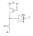
도 1의 (a-1)에 나타낸 반도체 장치에서, 제1 선(1st Line)은 트랜지스터(160)의 소스 전극에 전기적으로 접속되고, 제2 선(2nd Line)은 트랜지스터(160)의 드레인 전극에 전기적으로 접속된다. 트랜지스터(160)의 게이트 전극과, 트랜지스터(162)의 소스 전극 및 드레인 전극 중 하나는, 용량 소자(164)의 전극들 중 하나에 전기적으로 접속된다. 제3 선(3rd Line)은 트랜지스터(162)의 소스 전극 및 드레인 전극 중 다른 하나에 전기적으로 접속되고, 제4 선(4th Line)은 트랜지스터(162)의 게이트 전극에 전기적으로 접속된다. 제5 선(5th Line)은 용량 소자(164) 전극들 중 다른 하나에 전기적으로 접속된다.1, the first line (1st Line) is electrically connected to the source electrode of the
여기서, 산화물 반도체를 포함하는 트랜지스터가 트랜지스터(162)로서 이용된다. 산화물 반도체를 포함하는 트랜지스터는 상당히 작은 오프 전류 특성을 가진다. 따라서, 트랜지스터(162)가 오프일 때, 트랜지스터(160)의 게이트 전극의 전위는 극히 장기간 유지될 수 있다. 용량 소자(164)의 제공은 트랜지스터(160)의 게이트 전극에 부여된 전하의 유지와 저장된 데이터의 판독을 용이하게 한다. 산화물 반도체를 포함하는 트랜지스터(162)는 10 nm이상 1000 nm이하의 채널 길이(L)를 가진다; 따라서, 전력 소비가 작고 동작 속도가 극히 빠르다는 점에 유의한다.Here, a transistor including an oxide semiconductor is used as the
도 1의 (a-1)에 나타낸 반도체 장치는 트랜지스터(160)의 게이트 전극의 전위가 유지될 수 있는 특성을 이용함으로써, 다음과 같이 데이터를 기입, 저장, 및 판독한다.The semiconductor device shown in (a-1) in FIG. 1 writes, stores, and reads data by using the characteristic that the potential of the gate electrode of the
우선, 데이터의 기입 및 저장을 설명한다. 제4 선의 전위는 트랜지스터(162)를 온으로 하는 전위에 설정되어, 트랜지스터(162)가 온으로 된다. 따라서, 제3 선의 전위가 트랜지스터(160)의 게이트 전극과 용량 소자(164)에 공급된다. 즉, 트랜지스터(160)의 게이트 전극에 미리결정된 전하가 부여된다(기입). 여기서는, 2개의 상이한 전위를 공급하는 전하(이하 로우 레벨 전하, 및 하이 레벨 전하라고 함) 중 하나가 트랜지스터(160)의 게이트 전극에 부여된다. 그 후, 제4 선의 전위는 트랜지스터(162)를 오프로 하는 전위에 설정되어, 트랜지스터(162)가 오프로 된다. 따라서, 트랜지스터(160)의 게이트 전극에 부여된 전하가 유지된다(유지).First, the writing and storing of data will be described. The potential of the fourth line is set to the potential for turning on the
트랜지스터(162)의 오프 전류는 상당히 작기 때문에, 트랜지스터(160)의 게이트 전극의 전하는 장기간 유지된다.Since the off current of the
그 다음, 데이터의 판독을 설명한다. 제1 선에 미리결정된 전위(일정한 전위)를 공급하면서 제5 선에 적절한 전위(판독 전위)를 공급함으로써, 트랜지스터(160)의 게이트 전극에 유지된 전하량에 따라 제2 선의 전위가 변동한다. 이것은, 일반적으로, 트랜지스터(160)가 n채널 트랜지스터일 때, 트랜지스터(160)의 게이트 전극에 하이(High) 레벨 전하가 부여되는 경우의 피상 임계 전압(apparent threshold voltage)(Vth _H)은, 트랜지스터(160)의 게이트 전극에 로우(Low) 레벨 전하가 부여되는 경우의 피상 임계 전압(Vth _L)보다 낮기 때문이다. 여기서, 피상 임계 전압이란, 트랜지스터(160)를 온으로 하는 데 필요한 제5 선의 전위를 말한다. 따라서, 제5 선의 전위가 Vth _H와 Vth _L 사이의 중간 전위 V0으로 설정됨으로써, 트랜지스터(160)의 게이트 전극에 부여된 전하가 판별될 수 있다. 예를 들어, 기입시에, 하이 레벨 전하가 부여되는 경우, 제5 선의 전위가 V0(>Vth _H)에 설정되면, 트랜지스터(160)는 온으로 된다. 기입시에, 로우 레벨 전하가 부여되는 경우, 제5 선의 전위가 V0(< Vth _L)로 설정되더라도, 트랜지스터(160)는 오프 상태에 머문다. 따라서, 저장된 데이터는 제2 선의 전위를 이용하여 판독될 수 있다.Next, data reading will be described. The potential of the second line fluctuates depending on the amount of charge held in the gate electrode of the
메모리 셀을 어레이화하여 이용하는 경우, 소망 메모리 셀의 데이터만이 판독될 필요가 있다는 점에 유의한다. 따라서, 미리결정된 메모리 셀의 데이터가 판독되고 그 이외의 메모리 셀의 데이터는 판독되지 않게 하기 위해, 트랜지스터(160)가 메모리 셀들 사이에서 병렬에 접속되고 있는 경우에는, 데이터 판독의 대상이 아닌 메모리 셀의 제5 선에는, 게이트 전극의 상태에 관계없이 트랜지스터(160)를 오프로 하는 전위, 즉, Vth _H보다 낮은 전위가 공급될 수도 있다. 또한, 트랜지스터(160)가 메모리 셀들 사이에서 직렬로 접속된 경우에는, 데이터 판독의 대상이 아닌 메모리 셀의 제5 선에는, 게이트 전극의 상태에 관계없이 트랜지스터(160)를 온으로 하는 전위, 즉, Vth_L보다 높은 전위가 공급될 수도 있다.Note that when the memory cells are used in an array, only the data of the desired memory cell needs to be read out. Therefore, when the
그 다음, 데이터의 재기입을 설명한다. 데이터의 재기입은 데이터의 기입 및 유지와 유사한 방식으로 행해진다. 즉, 제4 선의 전위는 트랜지스터(162)를 온으로 하는 전위에 설정되어, 트랜지스터(162)가 온으로 된다. 따라서, 제3 선의 전위(새로운 데이터에 관련된 전위)가 트랜지스터(160)의 게이트 전극과 용량 소자(164)에 공급된다. 그 후, 제4 선의 전위는 트랜지스터(162)를 오프로 하는 전위에 설정되어, 트랜지스터(162)가 오프로 된다. 따라서, 트랜지스터(160)의 게이트 전극에는 새로운 데이터에 관련된 전하가 부여된다.Next, the rewriting of data will be described. The rewriting of data is performed in a manner similar to the writing and maintenance of data. That is, the potential of the fourth line is set to the potential for turning on the
개시된 발명에 따른 반도체 장치에서, 전술된 바와 같은 데이터의 또 다른 기입에 의해 데이터가 직접 재기입될 수 있다. 따라서, 플래시 메모리 등에서 필요한 고전압을 이용한 플로팅 게이트로부터의 전하의 추출은 불필요하고, 소거 동작에 기인한 동작 속도의 저하가 억제될 수 있다. 즉, 반도체 장치의 고속 동작이 실현될 수 있다.In the semiconductor device according to the disclosed invention, the data can be directly rewritten by another write of the data as described above. Therefore, the extraction of the charge from the floating gate using the high voltage necessary in the flash memory or the like is unnecessary, and the lowering of the operation speed due to the erase operation can be suppressed. That is, a high-speed operation of the semiconductor device can be realized.
트랜지스터(162)의 소스 전극 또는 드레인 전극이 트랜지스터(160)의 게이트 전극에 전기적으로 접속됨으로써, 비휘발성 메모리 소자에 이용되는 플로팅 게이트형 트랜지스터의 플로팅 게이트와 유사한 효과를 가진다는 점에 유의한다. 따라서, 도면에서 트랜지스터(162)의 소스 전극 또는 드레인 전극이 트랜지스터(160)의 게이트 전극에 전기적으로 접속되는 부분을 일부 경우에서는 플로팅 게이트부(FG)라고 부른다. 트랜지스터(162)가 오프인 경우, 플로팅 게이트부(FG)는 절연체에 매립된 것으로 간주될 수 있으므로 플로팅 게이트부(FG)에는 전하가 유지된다. 산화물 반도체를 포함하는 트랜지스터(162)의 오프 전류의 양은, 실리콘 등을 포함하는 트랜지스터의 오프 전류의 양의 10만 분의 1 이하이다; 따라서, 트랜지스터(162)의 리크 전류로 인해 플로팅 게이트부(FG)에 축적되는 전하의 소실은 무시할만한 정도이다. 즉, 산화물 반도체를 포함하는 트랜지스터(162)에 의해, 전력의 공급이 없어도 데이터를 저장할 수 있는 비휘발성 메모리 장치가 실현될 수 있다.Note that the source electrode or the drain electrode of the
예를 들어, 실온에서 트랜지스터(162)의 오프 전류가 10 zA/㎛(1 zA(젭토암페어)는 1×10-21 A임) 이하이고 용량 소자(164)의 용량값이 약 10 fF인 경우, 데이터는 104초 이상 저장될 수 있다. 물론, 저장 시간은 트랜지스터 특성 및 용량값에 의존한다.For example, when the off current of the
또한, 그 경우, 종래의 플로팅 게이트형 트랜지스터에서 지적되고 있는 게이트 절연막(터널 절연막)의 열화의 문제가 존재하지 않는다. 즉, 종래부터 문제로 여겨져 왔던, 플로팅 게이트로의 전자의 주입에 기인한 게이트 절연막의 열화가 해결될 수 있다. 이것은, 원리상 기입 회수에 제한이 없다는 것을 의미한다. 또한, 종래의 플로팅 게이트형 트랜지스터에서 기입이나 소거에 필요한 고전압이 불필요하다.In this case, there is no problem of deterioration of the gate insulating film (tunnel insulating film) pointed out in the conventional floating gate type transistor. That is, deterioration of the gate insulating film due to injection of electrons into the floating gate, which has been regarded as a problem in the past, can be solved. This means that there is no restriction on the number of entries in principle. In addition, a high voltage required for writing or erasing in the conventional floating gate type transistor is unnecessary.
도 1의 (a-1)의 반도체 장치 내의 트랜지스터 등의 구성요소는, 도 1의 (a-2)에 도시된 바와 같이 저항과 용량 소자를 포함하는 것으로 간주될 수 있다. 즉, 도 1의 (a-2)에서, 트랜지스터(160)와 용량 소자(164)는, 각각, 저항과 용량 소자를 포함하는 것으로 간주된다. R1과 C1은, 각각, 용량 소자(164)의 저항값과 용량값이다. 저항값(R1)은, 용량 소자(164)에 포함된 절연층에 의존하는 저항값에 대응한다. R2와 C2는, 각각, 트랜지스터(160)의 저항값과 용량값이다. 저항값(R2)은 트랜지스터(160)가 온 일때 게이트 절연층에 의존하는 저항값에 대응한다. 용량값(C2)은 소위 게이트 용량(게이트 전극과 소스 전극이나 드레인 전극 사이에 형성되는 용량, 및 게이트 전극과 채널 형성 영역 사이에 형성되는 용량)의 용량값에 대응한다.Components such as transistors in the semiconductor device of (a-1) of Fig. 1 can be regarded as including a resistor and a capacitive element as shown in Fig. 1 (a-2). That is, in (a-2) of Fig. 1, the
트랜지스터(162)가 오프인 경우의 소스 전극과 드레인 전극의 사이의 저항값(실효 저항이라고도 함)을 ROS라 할 경우, 트랜지스터(162)의 게이트 리크(gate leakage)가 충분히 작고 R1이 ROS 이상이고, R2가 ROS 이상인 조건 하에서, 전하 유지 기간(데이터 저장 기간이라고 함)은, 주로 트랜지스터(162)의 오프 전류에 의해 결정된다.When the resistance value (also referred to as effective resistance) between the source electrode and the drain electrode in the case where the
반면, 상기 조건을 만족하지 않는 경우에는, 트랜지스터(162)의 오프 전류가 충분히 작아도 유지 기간을 충분히 확보하는 것이 어렵다. 이것은, 트랜지스터(162)의 오프 전류 이외의 리크 전류(예를 들어, 소스 전극과 게이트 전극의 사이에서 발생하는 리크 전류)가 크기 때문이다. 따라서, 본 실시형태에서 개시되는 반도체 장치는 상기 관계를 만족하는 것이 바람직하다고 말할 수 있다.On the other hand, when the above condition is not satisfied, it is difficult to sufficiently maintain the sustain period even if the off current of the
C1이 C2 이상인 것이 바람직하다. C1이 크다면, 플로팅 게이트부(FG)의 전위가 제5 선에 의해 제어될 때(예를 들어, 판독시), 제5 선의 전위 변동이 억제될 수 있다.C1 is preferably C2 or more. If C1 is large, the potential fluctuation of the fifth line can be suppressed when the potential of the floating gate portion FG is controlled by the fifth line (for example, at the time of reading).
상기 관계가 만족되면, 더욱 양호한 반도체 장치를 실현할 수 있다. R1 및 R2는, 트랜지스터(160)와 트랜지스터(162)의 게이트 절연층들에 의해 제어된다는 점에 유의한다. 이것은 C1 및 C2에 대해서도 적용된다. 따라서, 게이트 절연층의 재료, 두께 등을 적절히 설정하여, 상기 관계를 만족시키는 것이 바람직하다.If the above relationship is satisfied, a better semiconductor device can be realized. Note that R1 and R2 are controlled by the gate insulating layers of
본 실시형태에서 설명되는 반도체 장치에서, 플로팅 게이트부(FG)가 플래시 메모리 등의 플로팅 게이트형 트랜지스터의 플로팅 게이트와 유사한 효과를 갖지만, 본 실시형태의 플로팅 게이트부(FG)는 플래시 메모리 등의 플로팅 게이트와는 본질적으로 다른 특징을 가진다. 플래시 메모리의 경우, 제어 게이트(control gate)에 인가되는 전압이 높기 때문에, 그 전위가 인접 셀의 플로팅 게이트에 영향을 미치는 것을 방지하기 위하여 셀들 사이에 적절한 간격을 유지하는 것이 필요하다. 이것은 반도체 장치의 고집적화를 저해하는 요인들 중 하나이다. 이 요인은, 고전계 인가시에 터널링 전류가 흐르는, 플래시 메모리의 기본 원리에 기인하는 것이다.In the semiconductor device described in this embodiment mode, the floating gate portion FG has an effect similar to that of a floating gate type transistor such as a flash memory. However, the floating gate portion FG of this embodiment has a floating It has features that are essentially different from gates. In the case of a flash memory, since the voltage applied to the control gate is high, it is necessary to maintain a proper gap between the cells in order to prevent the potential from affecting the floating gate of the adjacent cell. This is one of the factors impeding the high integration of the semiconductor device. This factor is due to the basic principle of the flash memory, in which the tunneling current flows at the time of application of a high-current system.
또한, 플래시 메모리의 상기 원리 때문에, 절연막의 열화가 진행하여 재기입 회수에 관한 제한(약 104 내지 105회)이라는 또 다른 문제가 발생한다.Further, due to the above-described principle of the flash memory, deterioration of the insulating film proceeds and another problem occurs (about 10 4 to 10 5 times) about the number of rewriting.
개시된 발명에 따른 반도체 장치는, 산화물 반도체를 포함하는 트랜지스터의 스위칭에 의해 동작하며, 전술된 터널링 전류에 의한 전하 주입의 원리를 이용하지 않는다. 즉, 플래시 메모리와는 달리, 전하 주입을 위한 고전계가 불필요하다. 따라서, 인접 셀에 미치는 컨트롤 게이트로부터의 고전계의 영향을 고려할 필요가 없고, 이것은 고집적화를 용이하게 한다.The semiconductor device according to the disclosed invention operates by switching of a transistor including an oxide semiconductor and does not use the principle of charge injection by the above-described tunneling current. That is, unlike the flash memory, a high electric field for charge injection is unnecessary. Therefore, it is not necessary to consider the influence of the high electric field from the control gate on the adjacent cell, which facilitates high integration.
또한, 터널링 전류에 의한 전하 주입을 이용하지 않기 때문에, 이것은 메모리 셀의 열화 원인이 존재하지 않는다는 것을 의미한다. 즉, 개시된 발명에 따른 반도체 장치는 플래시 메모리보다 높은 내구성과 신뢰성을 가진다.Further, since charge injection by the tunneling current is not used, this means that there is no cause of deterioration of the memory cell. That is, the semiconductor device according to the disclosed invention has higher durability and reliability than the flash memory.
또한, 플래시 메모리에 비하여, 고전계가 불필요하고 대형의 주변 회로(승압 회로 등)가 불필요하다는 점도 이점이다.Also, it is advantageous in that a large electric field is unnecessary and a large peripheral circuit (a booster circuit or the like) is unnecessary compared with a flash memory.
용량 소자(164)에 포함된 절연층의 비유전율(εr1)이 트랜지스터(160)에 포함된 절연층의 비유전율(εr2)과 상이한 경우, 용량 소자(164)에 포함된 절연층의 면적(S1)과 트랜지스터(160)의 게이트 용량 소자에 포함되는 절연층의 면적(S2)이, 2×S2가 S1이상(바람직하게는 S2가 S1이상)을 만족하면서 C1이 C2이상을 만족시키는 것이 용이하다. 즉, 용량 소자(164)에 포함되는 절연층의 면적을 줄이면서 C1이 C2이상을 만족시키는 것이 용이하다. 구체적으로는, 예를 들어, 산화 하프늄 등의 하이-k(high-k) 재료로 형성된 막, 또는 산화 하프늄 등의 하이-k(high-k) 재료로 형성된 막과 산화물 반도체로 형성된 막의 적층 구조를 용량 소자에 포함되는 절연층에 이용하여 εr1을 10 이상, 바람직하게는 15 이상으로 설정할 수 있고, 게이트 용량 소자에 포함되는 절연층에 대해 산화 실리콘을 이용하여 εr2를 3 내지 4로 설정할 수 있다.When the relative dielectric constant epsilon r1 of the insulating layer included in the
이러한 구조의 조합은, 개시된 발명에 따른 반도체 장치의 고집적화를 가능하게 한다.The combination of these structures enables high integration of the semiconductor device according to the disclosed invention.
상기 설명에서는 전자가 다수 캐리어인 n-채널 트랜지스터가 이용되었다; n-채널 트랜지스터 대신해 정공이 다수 캐리어인 p-채널 트랜지스터가 이용될 수 있다는 것은 말할 필요도 없다는 점에 유의한다.In the above description, an n-channel transistor in which electrons are majority carriers has been used; Note that it is needless to say that a p-channel transistor in which holes are majority carriers instead of an n-channel transistor can be used.
전술된 바와 같이, 개시된 발명의 한 실시형태에 따른 반도체 장치는, 오프 상태에서 소스와 드레인 사이의 리크 전류(오프 전류)가 작은 기입용 트랜지스터와, 기입용 트랜지스터와는 상이한 반도체 재료로 형성된 판독용 트랜지스터와, 용량 소자를 포함하는 비휘발성 메모리 셀을 가지고 있다.As described above, the semiconductor device according to one embodiment of the disclosed invention includes: a write transistor having a small leakage current (off current) between a source and a drain in an off state; and a read transistor formed of a semiconductor material different from the write transistor A transistor, and a non-volatile memory cell including a capacitor.
기입용 트랜지스터의 오프 전류는, 주변 온도(예를 들어, 25℃)에서 100 zA(1×10-19 A) 이하, 바람직하게는 10 zA(1×10-20 A) 이하, 더욱 바람직하게는, 1 zA(1×10-21 A) 이하이다. 일반적인 실리콘의 경우, 전술된 바와 같이 낮은 오프 전류를 달성하는 것은 어렵다. 그러나, 적절한 조건 하에서 산화물 반도체를 가공함으로써 얻어진 트랜지스터에서는, 작은 오프 전류가 달성될 수 있다. 따라서, 산화물 반도체를 포함하는 트랜지스터가 기입용 트랜지스터로서 이용되는 것이 바람직하다.The off current of the write transistor is set to 100 zA (1 x 10 -19 A) or less, preferably 10 zA (1 x 10 -20 A) or less at ambient temperature (for example, 25 ° C) , 1 zA (1 x 10 -21 A) or less. In the case of typical silicon, it is difficult to achieve a low off current as described above. However, in a transistor obtained by processing an oxide semiconductor under appropriate conditions, a small off current can be achieved. Therefore, it is preferable that a transistor including an oxide semiconductor is used as a write transistor.
또한, 산화물 반도체를 포함하는 트랜지스터는 작은 임계이하 스윙(S 값)을 가지므로, 이동도가 비교적 낮더라도 스위칭 속도가 충분히 높을 수 있다. 따라서, 이 트랜지스터를 기입용 트랜지스터로서 이용함으로써, 플로팅 게이트부(FG)에 부여되는 기입 펄스의 상승(rise)이 매우 가파를 수 있다. 또한, 오프 전류가 작기 때문에 플로팅 게이트부(FG)에 유지되는 전하량을 줄일 수 있다. 즉, 산화물 반도체를 포함하는 트랜지스터를 기입용 트랜지스터로서 이용함으로써, 데이터의 재기입이 고속으로 행해질 수 있다.Further, since the transistor including the oxide semiconductor has a small threshold swing (S value), the switching speed can be sufficiently high even if the mobility is relatively low. Therefore, by using this transistor as the write transistor, the rise of the write pulse applied to the floating gate portion FG can be very sharp. In addition, since the off current is small, the amount of charge held in the floating gate portion FG can be reduced. That is, by using a transistor including an oxide semiconductor as a write transistor, data can be rewritten at a high speed.
판독용 트랜지스터에 대해서는, 오프 전류에 관한 제한은 없지만, 판독 속도를 높이기 위해 고속으로 동작하는 트랜지스터를 이용하는 것이 바람직하다. 예를 들어, 1 나노초의 스위칭 속도 또는 더 빠른 속도를 갖는 트랜지스터를 판독용 트랜지스터로서 이용하는 것이 바람직하다.As for the reading transistor, there is no limitation on the off current, but it is preferable to use a transistor that operates at high speed to increase the reading speed. For example, it is preferable to use a transistor having a switching speed of 1 nanosecond or a higher speed as a reading transistor.
기입용 트랜지스터를 온으로 함으로써 메모리 셀에 데이터를 기입하여, 기입용 트랜지스터의 소스 전극 및 드레인 전극 중 하나와, 용량 소자의 전극들 중 하나와, 판독용 트랜지스터의 게이트 전극이 서로 전기적으로 접속되어 있는 노드에 전위를 공급한 다음, 기입용 트랜지스터를 오프로 하여 미리결정된 양의 전하를 노드에 유지한다. 여기서, 기입용 트랜지스터의 오프 전류는 극히 작다; 따라서, 노드에 공급된 전하는 장기간 유지된다. 오프 전류가, 예를 들어, 실질적으로 0이면, 종래의 DRAM에서 요구되는 리프레시 동작이 불필요하거나, 리프레시 동작의 빈도가 상당히 낮아질(예를 들어, 약 1달이나 1년에 한 번) 수 있다. 따라서, 반도체 장치의 전력 소비가 충분히 저감될 수 있다.The writing transistor is turned on to write data to the memory cell so that one of the source electrode and the drain electrode of the writing transistor and one of the electrodes of the capacitor and the gate electrode of the reading transistor are electrically connected to each other Supplies a potential to the node, and then turns off the write transistor to hold a predetermined amount of charge at the node. Here, the off current of the write transistor is extremely small; Thus, the charge supplied to the node is maintained for a long time. If the off current is, for example, substantially zero, the refresh operation required in the conventional DRAM may be unnecessary, or the frequency of the refresh operation may be significantly lowered (for example, about once a month or once a year). Therefore, the power consumption of the semiconductor device can be sufficiently reduced.
또한, 메모리 셀에 새로운 데이터를 덮어쓰기(overwrite)함으로써 데이터가 직접 재기입될 수 있다. 이 때문에, 플래시 메모리 등에서 필요한 소거 동작이 필요하지 않아, 소거 동작에 기인한 동작 속도의 저하가 방지될 수 있다. 즉, 반도체 장치의 고속 동작이 실현될 수 있다. 또한, 종래의 플로팅 게이트형 트랜지스터가 데이터를 기입 및 소거하는 데 필요한 고전압이 불필요하다; 따라서, 반도체 장치의 전력 소비가 더욱 저감될 수 있다. 본 실시형태에 따른 메모리 셀에 인가되는 가장 높은 전압(메모리 셀의 각 단자에 동시에 인가되는 최고 전위와 최저 전위 사이의 차이)은, 2 단계(1 비트)의 데이터가 기입되는 경우 각각의 메모리 셀에서, 5 V 이하, 바람직하게는 3 V 이하이다.In addition, data can be directly rewritten by overwriting new data in the memory cell. Therefore, a necessary erasing operation is not required in the flash memory or the like, and a reduction in the operating speed due to the erasing operation can be prevented. That is, a high-speed operation of the semiconductor device can be realized. In addition, a high voltage required for a conventional floating gate type transistor to write and erase data is unnecessary; Therefore, the power consumption of the semiconductor device can be further reduced. (The difference between the highest potential and the lowest potential which are simultaneously applied to the respective terminals of the memory cell) applied to the memory cell according to the present embodiment is such that when data of two stages (one bit) is written, 5 V or less, preferably 3 V or less.
개시된 발명에 따른 반도체 장치에 제공되는 메모리 셀은, 적어도 기입용 트랜지스터, 판독용 트랜지스터, 및 용량 소자를 포함할 수도 있다. 또한, 용량 소자의 면적이 작아도 메모리 셀이 동작할 수 있다. 따라서, 예를 들어, 각 메모리 셀에서 6개의 트랜지스터를 요구하는 SRAM에 비해, 각 메모리 셀의 면적이 충분히 작아질 수 있다; 따라서, 반도체 장치에서 메모리 셀들이 고밀도로 배치될 수 있다.The memory cell provided in the semiconductor device according to the disclosed invention may include at least a writing transistor, a reading transistor, and a capacitor. Also, the memory cell can operate even if the area of the capacitor element is small. Thus, for example, the area of each memory cell can be sufficiently small compared to an SRAM requiring six transistors in each memory cell; Therefore, the memory cells in the semiconductor device can be arranged at a high density.
종래의 플로팅 게이트형 트랜지스터에서는, 기입 동작 동안에 게이트 절연막(터널 절연막)에서 전하가 이동하여, 그 게이트 절연막(터널 절연막)의 열화가 불가피하다. 대조적으로, 본 발명의 한 실시형태에 따른 메모리 셀에서는, 기입용 트랜지스터의 스위칭 동작에 의해 데이터가 기입된다; 따라서, 종래부터 문제라고 인식되어 왔던 게이트 절연막의 열화가 무시될 수 있다. 이것은, 원리상 기입 횟수에 제한이 없으며 기입 내구성이 매우 높다는 것을 의미한다. 예를 들어, 본 발명의 한 실시형태에 따른 메모리 셀에서는, 1×10⁹회 이상(10억회 이상) 데이터가 기입된 후에도 전류-전압 특성이 열화되지 않는다.In the conventional floating gate type transistor, charge moves in the gate insulating film (tunnel insulating film) during the writing operation, and deterioration of the gate insulating film (tunnel insulating film) is inevitable. In contrast, in the memory cell according to the embodiment of the present invention, the data is written by the switching operation of the writing transistor; Therefore, deterioration of the gate insulating film, which has been conventionally recognized as a problem, can be ignored. This means that there is no restriction on the number of writing in principle and the writing durability is very high. For example, in the memory cell according to the embodiment of the present invention, the current-voltage characteristic does not deteriorate even after data of 1 x 10 9 or more (1 billion times or more) is written.
또한, 메모리 셀의 기입용 트랜지스터로서 산화물 반도체를 포함하는 트랜지스터를 이용하는 경우, 산화물 반도체는 3.0 eV 내지 3.5 eV의 넓은 에너지 갭을 가지며 극히 적은 수의 열적으로 여기된 캐리어를 포함하기 때문에, 예를 들어, 150℃의 고온에서도 메모리 셀의 전류-전압 특성이 열화되지 않는다.Further, in the case of using a transistor including an oxide semiconductor as a transistor for writing a memory cell, since the oxide semiconductor has a wide energy gap of 3.0 eV to 3.5 eV and contains an extremely small number of thermally excited carriers, , The current-voltage characteristic of the memory cell does not deteriorate even at a high temperature of 150 캜.
본 발명자들은, 산화물 반도체를 포함하는 트랜지스터는, 150℃의 고온에서도 특성이 열화되지 않고, 오프 전류가 극히 작은 100 zA이하라는 우수한 특성을 갖는다는 것을 처음으로 발견했다. 개시된 발명의 한 실시형태는, 이러한 우수한 특성을 갖는 트랜지스터를 메모리 셀의 기입용 트랜지스터로서 이용함으로써, 신규한 특징을 갖는 반도체 장치를 제공하는 것이다.The present inventors have found for the first time that a transistor including an oxide semiconductor has excellent characteristics such that the characteristic does not deteriorate even at a high temperature of 150 캜 and the off current is extremely small, that is, 100 zA or less. An embodiment of the disclosed invention provides a semiconductor device having novel characteristics by using a transistor having such excellent characteristics as a transistor for writing a memory cell.
전술된 바와 같이, 본 실시형태에서 설명된 구조, 방법 등은 다른 실시형태들에서 설명된 구조, 방법 등과 적절히 조합될 수 있다.As described above, the structures, methods, and the like described in this embodiment can be appropriately combined with structures, methods, and the like described in the other embodiments.
(실시형태 2)(Embodiment 2)
본 실시형태에서는, 상기 실시형태에서 설명된 반도체 장치의 응용예를 설명한다. 구체적으로는, 상기 실시형태에서 설명된 반도체 장치가 매트릭스로 배열된 반도체 장치의 예를 설명한다.In this embodiment, an application example of the semiconductor device described in the above embodiment will be described. Specifically, an example of a semiconductor device in which the semiconductor devices described in the above embodiments are arranged in a matrix will be described.
도 2는 m×n 비트의 메모리 용량을 포함하는 반도체 장치의 회로도의 예이다.2 is an example of a circuit diagram of a semiconductor device including a memory capacity of m x n bits.
본 발명의 한 실시형태에 따른 반도체 장치는, m개의 워드선(WL), m개의 신호선(S), n개의 비트선(BL), n개의 소스선(SL), 및 m개(행)(수직 방향) × n개(열)(수평 방향)(m 및 n은 자연수)의 매트릭스로 배치된 복수의 메모리 셀(1100),을 포함하는 메모리 셀 어레이와, 제1 구동 회로(1111), 제2 구동 회로(1112), 제3 구동 회로(1113), 및 제4 구동 회로(1114) 등의 주변 회로를 포함한다. 여기서, 상기 실시형태에서 설명된 구조(도 1의 (a-1)의 구조)가 메모리 셀(1100)에 적용된다.A semiconductor device according to an embodiment of the present invention includes m word lines WL, m signal lines S, n bit lines BL, n source lines SL, and m lines (rows) A plurality of
각 메모리 셀(1100)은, 제1 트랜지스터, 제2 트랜지스터, 및 용량 소자를 포함한다. 제1 트랜지스터의 게이트 전극, 제2 트랜지스터의 소스 전극 및 드레인 전극 중 하나, 및 용량 소자의 전극들 중 하나는 서로 전기적으로 접속된다. 소스선(SL), 제1 트랜지스터의 소스 전극, 및 제2 트랜지스터의 소스 전극 및 드레인 전극 중 다른 하나는 서로 전기적으로 접속된다. 비트선(BL)과 제1 트랜지스터의 드레인 전극은 서로 전기적으로 접속된다. 신호선(S)과 제2 트랜지스터의 게이트 전극은 서로 전기적으로 접속된다. 워드선(WL)과 용량 소자의 전극들 중 다른 하나는 서로 전기적으로 접속된다. 즉, 소스선(SL)은 도 1의 (a-1)에 나타낸 구조에서 제1 선(1st Line) 및 제3 선(3rd Line)에 대응하고, 비트선(BL)은 제2 선(2nd Line)에 대응하며, 신호선(S)은 제4 선(4th Line)에 대응하고, 워드선(WL)은 제5 선(5th Line)에 대응한다.Each
또한, 메모리 셀(1100)들은, 소스선(SL)과 비트선(BL) 사이에서 병렬로 접속된다. 예를 들어, i행 j열의 메모리 셀 1100(i, j)(i는 1 이상 m 이하의 정수, j는 1 이상 n 이하의 정수)는, 소스선 SL(j), 비트선 BL(j), 워드선 WL(i), 및 신호선 S(i)에 전기적으로 접속된다.Further, the
소스선(SL) 및 비트선(BL)은 스위칭 소자를 통해 제1 구동 회로(1111)에 전기적으로 접속된다. 소스선(SL)은 스위칭 소자를 제2 구동 회로(1112)에 전기적으로 접속된다. 신호선(S)은 제3 구동 회로(1113)에 전기적으로 접속된다. 워드선(WL)은 제4 구동 회로(1114)에 전기적으로 접속된다. 여기서, 제1 구동 회로(1111), 제2 구동 회로(1112), 제3 구동 회로(1113), 및 제4 구동 회로(1114)는 별개로 제공된다; 그러나, 개시된 발명은 이것으로 한정되지 않는다는 점에 유의한다. 하나의 기능이나 몇 개의 기능을 갖는 구동 회로가 대안으로서 이용될 수도 있다.The source line SL and the bit line BL are electrically connected to the
그 다음, 기입 동작 및 판독 동작을 설명한다. 도 3은 기입 동작 및 판독 동작의 타이밍도의 예이다.Next, the write operation and the read operation will be described. 3 is an example of a timing chart of a write operation and a read operation.
간소화를 위해 2행×2열의 메모리 셀 어레이의 반도체 장치의 동작을 설명할 것이지만, 개시된 발명은 이것으로 한정되지 않는다.The operation of the semiconductor device of the memory cell array of 2 rows x 2 columns will be described for simplification, but the disclosed invention is not limited to this.
제1 행의 메모리 셀 1100(1, 1) 및 메모리 셀 1100(1, 2)로의 데이터 기입과, 제1 행의 메모리 셀 1100(1, 1) 및 메모리 셀 1100(1, 2)로부터의 데이터 판독을 설명한다. 이하의 설명에서는, 메모리 셀 1100(1, 1)에 기입되는 데이터가 "1"이고 메모리 셀 1100(1, 2)에 기입되는 데이터는 "0"인 것으로 가정한다는 점에 유의한다.Data is written to the memory cells 1100 (1, 1) and the memory cells 1100 (1, 2) in the first row and data is written to the memory cells 1100 (1, The reading will be explained. In the following description, it is assumed that the data written to the memory cells 1100 (1, 1) is "1" and the data written to the memory cells 1100 (1, 2) is "0".
우선, 기입을 설명한다. 제1 행의 신호선 S(1)에 전위 V1이 공급되어 제1 행의 제2 트랜지스터가 온으로 된다. 또한, 제2 행의 신호선 S(2)에 전위 0 V가 공급되어 제2 행의 제2 트랜지스터가 오프로 된다.First, the writing will be described. The potential V1 is supplied to the signal line S (1) of the first row and the second transistor of the first row is turned on. A potential of 0 V is supplied to the signal line S (2) of the second row, and the second transistor of the second row is turned off.
그 다음, 전위 V1의 인가에 의해 스위칭 소자의 제어 신호 SSL_b(1)와 SSL_b(2)가 어서트(활성화)되고, 제2 구동 회로(1112)의 단자 SL_b(1)과 SL_b(2)가 소스선 SL(1)과 소스선 SL(2)에 전기적으로 접속된다. 여기서, SL_b(1)에는 전위 V2가 공급되고, SL_b(2)에는 전위 0 V가 공급된다.The control signals SSL_b (1) and SSL_b (2) of the switching elements are asserted (activated) by application of the potential V1 and the terminals SL_b (1) and SL_b (2) of the
그 결과, 메모리 셀 1100(1, 1)의 플로팅 게이트부(FG)와 메모리 셀 1100(1, 2)의 플로팅 게이트부(FG)에는 각각 전위 V2와 전위 0 V가 공급된다. 여기서, 전위 V2는 제1 트랜지스터의 임계 전압보다 높다. 또한, 제1 행의 신호선 S(1)의 전위는 0 V에 설정되어, 제1 행의 제2 트랜지스터가 오프로 된다. 따라서, 기입이 완료된다. 전위 V2는 전위 V1과 실질적으로 동일하거나 전위 V1 이하인 것이 바람직하다.As a result, the potential V2 and the potential 0V are supplied to the floating gate portion FG of the memory cell 1100 (1, 1) and the floating gate portion FG of the memory cell 1100 (1, 2), respectively. Here, the potential V2 is higher than the threshold voltage of the first transistor. Further, the potential of the signal line S (1) of the first row is set to 0 V, and the second transistor of the first row is turned off. Thus, the writing is completed. The potential V2 is preferably substantially equal to the potential V1 or lower than the potential V1.
워드선 WL(1) 및 WL(2)는 기입 동작 동안에 0 V로 설정된다는 점에 유의한다. 또한, 스위칭 소자의 제어 신호 SSL_a(1), SSL_a(2), SBL(1), 및 SBL(2)는 디어서트(비활성화) 된다. 또한, SL_b(1)의 전위가 변하기 전에 제1 행의 신호선 S(1)의 전위가 0 V로 설정된다. 기입 후에, 메모리 셀의 임계 전압은, 데이터 "0"의 경우에는 Vw0이고, 데이터 "1"의 경우에는 Vw1이다. 여기서, 메모리 셀의 임계 전압이란, 제1 트랜지스터의 소스 전극과 드레인 전극 사이의 저항을 변화시키는, 워드선(WL)에 전기적으로 접속된 단자의 전압을 의미한다. Vw0>0>Vw1을 만족한다는 점에 유의한다.It is noted that word lines WL (1) and WL (2) are set to 0 V during the write operation. In addition, the control signals SSL_a (1), SSL_a (2), SBL (1), and SBL (2) of the switching elements are deasserted (deactivated). Further, the potential of the signal line S (1) of the first row is set to 0 V before the potential of the SL_b (1) changes. After writing, the threshold voltage of the memory cell is Vw0 in the case of data "0" and Vw1 in the case of data "1". Here, the threshold voltage of the memory cell means a voltage of a terminal electrically connected to the word line WL, which changes the resistance between the source electrode and the drain electrode of the first transistor. Vw0 > 0 > Vw1.
또한, 스위칭 소자의 제어 신호 SSL_a(1), SSL_a(2), SBL(1), 및 SBL(2)가 디어서트(비활성화)되면, 비트선(BL)과 소스선(SL)에는, 제1 구동 회로(1111)로부터는 전위가 공급되지 않고, 제2 구동 회로(1112)의 단자(SL_b)로부터 전위가 공급된다. 따라서, 소스선(SL)에는 단자(SL_b)와 동일한 전위가 공급된다. 또한, 비트선(BL)에 전기적으로 접속된 메모리 셀의 제1 트랜지스터들 중 어떤 하나라도 온 상태이면 비트선(BL)은 소스선(SL)과 동일한 전위가 되는 반면, 모든 제1 트랜지스터가 오프 상태이면 비트선(BL)은 플로팅 상태가 된다. 도 3에 나타낸 타이밍도는 비트선(BL)이 소스선(SL)과 동일한 전위가 되는 경우를 나타낸다.When the control signals SSL_a (1), SSL_a (2), SBL (1), and SBL (2) of the switching elements are deasserted (deactivated), the bit lines BL and the source lines SL The potential is not supplied from the
본 기입 동작에서는, 스위칭 소자의 제어 신호 SBL(1) 및 SBL(2)는 디어서트(비활성화)되지만, 스위칭 소자의 제어 신호 SBL(1) 및 SBL(2)가 어서트(활성화) 될 수 있다는 점에 유의한다. 그 경우, 단자 BL_a(1)에는 단자 SL_b(1)과 동일한 전위가 공급되고, 단자 BL_a(2)에는 단자 SL_b(2)와 동일한 전위가 공급될 수도 있다.In this writing operation, the control signals SBL (1) and SBL (2) of the switching elements are deasserted (deactivated), but the control signals SBL (1) and SBL . In this case, the terminal BL_a (1) is supplied with the same potential as the terminal SL_b (1), and the terminal BL_a (2) is supplied with the same potential as the terminal SL_b (2).
그 다음, 판독을 설명한다. 여기서, 비트선(BL)은 도 4에 나타낸 판독 회로에 전기적으로 접속된다. 도 4에 나타낸 판독 회로에서, 비트선(BL)은, 판독 인에이블 신호(RE 신호)에 의해 제어되는 스위칭 소자를 통해, 클록형 인버터와, 전위 V1이 공급된 배선에 다이오드-접속된 트랜지스터에 전기적으로 접속된다.Next, the reading will be described. Here, the bit line BL is electrically connected to the read circuit shown in Fig. In the readout circuit shown in Fig. 4, the bit line BL is connected to the clocked inverter and the transistor diode-connected to the wiring to which the potential V1 is supplied through the switching element controlled by the read enable signal (RE signal) And is electrically connected.
우선, 제1 행의 워드선 WL(1) 및 제2 행의 워드선 WL(2)에는 각각 전위 0 V와 전위 VL이 공급된다. 전위 VL은 임계 전압 Vw1보다 낮다. 워드선 WL(1)이 전위 0 V이면, 제1 행에서, 데이터 "0"이 저장되어 있는 메모리 셀의 제1 트랜지스터는 오프로 되고, 데이터 "1"이 저장되어 있는 메모리 셀의 제1 트랜지스터는 온으로 된다. 워드선 WL(2)이 전위 VL이면, 제2 행에서, 데이터 "0" 또는 데이터 "1"이 저장되어 있는 메모리 셀의 제1 트랜지스터는 오프로 된다.First, the potential 0 V and the potential VL are supplied to the word line WL (1) of the first row and the word line WL (2) of the second row, respectively. The potential VL is lower than the threshold voltage Vw1. When the potential of the word line WL (1) is 0 V, in the first row, the first transistor of the memory cell storing the data "0 " is turned off and the first transistor Is turned on. When the word line WL (2) is at the potential VL, the first transistor of the memory cell storing data "0" or data "1" is turned off in the second row.
그 다음, 전위 V1의 인가에 의해 스위칭 소자의 제어 신호 SSL_a(1), SSL_a(2), SBL(1), 및 SBL(2)가 어서트(활성화) 된다. 제1 구동 회로(1111)의 단자 BL_a(1)과 BL_a(2)는 각각 비트선 BL(1)과 비트선 BL(2)에 전기적으로 접속된다. 제1 구동 회로(1111)의 단자 SL_a(1)과 SL_a(2)는 각각 소스선 SL(1)과 소스선 SL(2)에 전기적으로 접속된다. SL_a(1)과 SL_a(2)에는 전위 0 V가 공급된다. 또한, 판독 인에이블 신호(RE 신호)는 어서트된다(활성 상태).Then, the control signals SSL_a (1), SSL_a (2), SBL (1), and SBL (2) of the switching elements are asserted (activated) by application of the potential V1. The terminals BL_a (1) and BL_a (2) of the
그 결과, 단자 BL_a(1)과 단자 SL_a(1) 사이의 메모리 셀 1100(1, 1)의 트랜지스터는 온으로 됨으로써 저저항을 갖게 되고, 단자 BL_a(2)와 단자 SL_a(2) 사이의 메모리 셀 1100(1, 2)의 트랜지스터는 오프로 됨으로써, 고저항을 갖게 된다. 단자 BL_a(1)과 BL_a(2)에 전기적으로 접속된 판독 회로는, 비트선들 사이의 저항차에 기초하여 데이터를 판독할 수 있다. 스위칭 소자의 제어 신호 SSL_b(1)과 SSL_b(2)는 디어서트된다는 점에 유의한다.As a result, the transistors of the memory cell 1100 (1, 1) between the terminal BL_a (1) and the terminal SL_a (1) are turned on to have a low resistance and the memory between the terminal BL_a (2) and the terminal SL_a The transistors of the cells 1100 (1, 2) are turned off, thereby having a high resistance. The reading circuit electrically connected to the terminals BL_a (1) and BL_a (2) can read data based on the resistance difference between the bit lines. It should be noted that the control signals SSL_b (1) and SSL_b (2) of the switching elements are de-asserted.
판독 동작 동안에, 신호선 S(1)과 신호선 S(2)에는 각각 전위 0 V와 전위 VL이 공급되어, 모든 제2 트랜지스터가 오프로 된다는 점에 유의한다. 제1 행의 플로팅 게이트부(FG)의 전위는 0 V 또는 V2이다; 따라서, 신호선 S(1)의 전위가 0 V로 설정됨으로써, 모든 제2 트랜지스터가 오프로 될 수 있다. 한편, 제2 행의 플로팅 게이트부(FG)의 전위는, 워드선 WL(2)에 전위 VL이 공급되면, 기입 직후의 전위보다 낮게 된다. 따라서, 제2 행의 제2 트랜지스터가 온으로 되는 것을 방지하기 위하여, 신호선 S(2)의 전위가 워드선 WL(2)의 전위와 유사하게 낮은 전위(전위 VL)로 설정된다. 따라서, 모든 제2 트랜지스터가 오프로 될 수 있다.Note that, during the read operation, the potential 0 V and the potential VL are supplied to the signal line S (1) and the signal line S (2), respectively, and all the second transistors are turned off. The potential of the floating gate portion FG in the first row is 0 V or V2; Therefore, by setting the potential of the signal line S (1) to 0 V, all the second transistors can be turned off. On the other hand, when the potential VL is supplied to the word line WL2, the potential of the floating gate portion FG in the second row becomes lower than the potential immediately after writing. Therefore, in order to prevent the second transistor of the second row from being turned on, the potential of the signal line S (2) is set to a low potential (potential VL) similar to the potential of the word line WL (2). Thus, all the second transistors can be turned off.
그 다음, 판독 회로로서 도 4의 회로를 이용하는 경우의 출력 전위를 설명한다. 단자 BL_a(1)과 단자 SL_a(1) 사이의 저항은 낮기 때문에, 클록형 인버터에는 저전위가 공급되고 출력 D(1)은 신호 하이(high)이다. 단자 BL_a(2)와 단자 SL_a(2) 사이의 저항은 높기 때문에, 클록형 인버터에는 고전위가 입력되고 출력 D(2)는 신호 로우(low)이다.Next, the output potential when the circuit of Fig. 4 is used as the readout circuit will be described. Since the resistance between the terminal BL_a (1) and the terminal SL_a (1) is low, a low potential is supplied to the clocked inverter and an output D (1) is signal high. Since the resistance between the terminal BL_a (2) and the terminal SL_a (2) is high, the high potential is input to the clocked inverter and the output D (2) is low.
동작 전위는, 예를 들어, V1=2 V, V2=1.5 V, VH=2 V, 및 VL=-2 V로 설정될 수 있다.The operating potential can be set, for example, to V1 = 2 V, V2 = 1.5 V, VH = 2 V, and VL = -2 V.
상기 구조를 갖는 반도체 장치가 제조되면, 소스선(SL)이 메모리 셀의 플로팅 게이트부에 전위를 공급하는 배선으로서 기능하여, 각 메모리 셀의 배선수가 저감될 수 있다. 따라서, 메모리 셀의 면적이 저감될 수 있고 반도체 장치의 단위 면적당 메모리 용량이 증가될 수 있다.When the semiconductor device having the above structure is manufactured, the source line SL functions as a wiring for supplying a potential to the floating gate portion of the memory cell, so that the number of wiring lines of each memory cell can be reduced. Therefore, the area of the memory cell can be reduced and the memory capacity per unit area of the semiconductor device can be increased.
도 2에 나타낸 반도체 장치는 반도체를 포함하고, 이 반도체에 의해 형성된 트랜지스터는 극히 작은 오프 전류를 갖기 때문에, 저장된 데이터가 극히 장기간 유지될 수 있다. 즉, 리프레시 동작이 불필요해지거나 리프레시 동작의 빈도가 극히 낮아질 수 있기 때문에 전력 소비가 충분히 저감될 수 있다. 게다가, 전력이 공급되지 않는 경우에도 저장된 데이터가 장기간 유지될 수 있다.The semiconductor device shown in Fig. 2 includes a semiconductor, and since the transistor formed by this semiconductor has an extremely small off current, the stored data can be maintained for a very long time. That is, since the refresh operation becomes unnecessary or the frequency of the refresh operation can be extremely lowered, the power consumption can be sufficiently reduced. In addition, even if power is not supplied, stored data can be maintained for a long time.
또한, 도 2에 나타낸 반도체 장치에서는, 데이터의 기입에 고전압이 필요하지 않고, 소자의 열화의 문제도 없다. 따라서, 도 2에 나타낸 반도체 장치는 종래의 비휘발성 메모리에서 문제가 되고 있는 기입 횟수에 관한 제약을 갖지 않으며, 그 신뢰성이 극적으로 향상된다. 또한, 트랜지스터의 온 상태 및 오프 상태에 따라 데이터의 기입을 행하므로, 고속 동작이 용이하게 실현될 수 있다. 추가적으로, 데이터를 소거하는 동작이 불필요하다는 이점이 있다.Further, in the semiconductor device shown in Fig. 2, high voltage is not required to write data, and there is no problem of deterioration of elements. Therefore, the semiconductor device shown in Fig. 2 does not have a restriction on the number of times of writing that is problematic in the conventional nonvolatile memory, and its reliability is dramatically improved. Further, since data is written in accordance with the ON and OFF states of the transistor, high-speed operation can be easily realized. In addition, there is an advantage that the operation of erasing data is unnecessary.
산화물 반도체 이외의 재료를 포함하는 트랜지스터는 충분히 고속으로 동작할 수 있기 때문에, 반도체 장치는 산화물 반도체를 포함하는 트랜지스터와 조합하여 충분히 고속으로 동작(예를 들어, 데이터의 판독)을 행할 수 있다. 또한, 산화물 반도체 이외의 재료를 포함하는 트랜지스터는, 고속으로 동작할 것을 요구하는 각종 회로(예를 들어, 논리 회로나 구동 회로)를 양호하게 실현할 수 있다.Since a transistor including a material other than an oxide semiconductor can operate at a sufficiently high speed, the semiconductor device can operate at a sufficiently high speed (for example, reading data) in combination with a transistor including an oxide semiconductor. In addition, a transistor including a material other than an oxide semiconductor can satisfactorily realize various circuits (for example, a logic circuit and a drive circuit) that require operation at a high speed.
따라서, 산화물 반도체 이외의 재료를 포함하는 트랜지스터와 산화물 반도체를 포함하는 트랜지스터 양쪽 모두를 포함함으로써, 신규한 특징을 갖는 반도체 장치가 실현될 수 있다.Therefore, by including both the transistor including the material other than the oxide semiconductor and the transistor including the oxide semiconductor, a semiconductor device having novel characteristics can be realized.
본 실시형태에서는, 전술된 바와 같이 소스선(SL)과 제2 트랜지스터의 소스 전극 및 드레인 전극 중 다른 하나가 서로 전기적으로 접속되지만, 본 발명은 이것으로 한정되지 않는다. 도 5의 반도체 장치의 회로도에 나타낸 바와 같이, 비트선(BL)과 제2 트랜지스터의 소스 전극 및 드레인 전극 중 다른 하나는 서로 전기적으로 접속될 수도 있다. 그 경우, 소스선(SL)이 아니라 비트선(BL)이 스위칭 소자를 통해 제2 구동 회로(1112)에 전기적으로 접속된다. 여기서, 도 5에 나타낸 반도체 장치의 구조는, 비트선(BL)과 제2 트랜지스터의 소스 전극 및 드레인 전극 중 다른 하나가 서로 전기적으로 접속되고 있고 비트선(BL)이 스위칭 소자를 통해 제2 구동 회로(1112)에 전기적으로 접속되고 있다는 점을 제외하고는, 도 2에 나타낸 반도체 장치와 동일한 구조이다.In the present embodiment, the source line SL and the other of the source electrode and the drain electrode of the second transistor are electrically connected to each other as described above, but the present invention is not limited to this. As shown in the circuit diagram of the semiconductor device of Fig. 5, the bit line BL and the other of the source electrode and the drain electrode of the second transistor may be electrically connected to each other. In this case, the bit line BL, not the source line SL, is electrically connected to the
전술된 바와 같이, 본 실시형태에서 설명된 구조, 방법 등은 다른 실시형태들에서 설명된 구조, 방법 등과 적절히 조합될 수 있다.As described above, the structures, methods, and the like described in this embodiment can be appropriately combined with structures, methods, and the like described in the other embodiments.
(실시형태 3)(Embodiment 3)
본 실시형태에서는, 상기 실시형태에서 설명된 반도체 장치가 매트릭스로 배열된 반도체 장치의 또 다른 예를 설명한다.In this embodiment, another example of the semiconductor device in which the semiconductor devices described in the above embodiments are arranged in a matrix will be described.
도 6은 m×n 비트의 메모리 용량을 포함하는 반도체 장치의 회로도의 예이다.6 is an example of a circuit diagram of a semiconductor device including a memory capacity of m x n bits.
본 발명의 한 실시형태에 따른 반도체 장치는, m개의 워드선(WL), m개의 신호선(S), n개의 비트선(BL), n2개의 소스선(SL), 및 복수의 메모리 셀(1200)이 m개(행)(수직 방향) × n개(열)(수평 방향)의 매트릭스로 배치된 메모리 셀 어레이와, 제1 구동 회로(1211), 제2 구동 회로(1212), 제3 구동 회로(1213), 및 제4 구동 회로(1214) 등의 주변 회로를 포함한다(m, n, 및 n2는 자연수, n2는 n/2이상의 최소의 자연수). 여기서, 상기 실시형태에서 설명된 구조(도 1의 (a-1)의 구조)가 메모리 셀(1200)에 적용된다.A semiconductor device according to an embodiment of the present invention includes m word lines WL, m signal lines S, n bit lines BL, n2 source lines SL, and a plurality of memory cells 1200 ) Arranged in a matrix of m (rows) (vertical direction) x n rows (columns) (horizontal direction), and a plurality of memory cells arranged in a matrix of
각 메모리 셀(1200)은, 제1 트랜지스터, 제2 트랜지스터, 및 용량 소자를 포함한다. 제1 트랜지스터의 게이트 전극, 제2 트랜지스터의 소스 전극 및 드레인 전극 중 하나, 및 용량 소자의 전극들 중 하나는 서로 전기적으로 접속된다. 소스선(SL)과 제1 트랜지스터의 소스 전극은 서로 전기적으로 접속된다. 비트선(BL), 제1 트랜지스터의 드레인 전극, 및 제2 트랜지스터의 소스 전극 및 드레인 전극 중 다른 하나는 서로 전기적으로 접속된다. 신호선(S)과 제2 트랜지스터의 게이트 전극은 서로 전기적으로 접속된다. 워드선(WL)과 용량 소자의 전극들 중 다른 하나는 서로 전기적으로 접속된다. 즉, 소스선(SL)은 도 1의 (a-1)에 나타낸 구조에서 제1 선(1st Line)에 대응하고, 비트선(BL)은 제2 선(2nd Line) 및 제3 선(3rd Line)에 대응하며, 신호선(S)은 제4 선(4th Line)에 대응하고, 워드선(WL)은 제5 선(5th Line)에 대응한다.Each
또한, 메모리 셀(1200)들은, 소스선(SL)과 비트선(BL) 사이에서 병렬로 접속된다. 예를 들어, i행 j열의 메모리 셀 1200(i, j)(i는 1이상 m이하의 정수, j는 1이상 n이하의 정수)는, 소스선 SL(j2), 비트선 BL(j), 워드선 WL(i), 및 신호선 S(i)에 각각 전기적으로 접속된다(j2는 j/2이상의 최소의 자연수). 즉, 서로 인접하는 메모리 셀인, 메모리 셀 1200(i, 2k-1)과 메모리 셀 1200(i, 2k)은, 동일한 소스선 SL(k)에 전기적으로 접속된다(k는 1이상 n/2 이하의 자연수).Further, the
소스선(SL) 및 비트선(BL)은 스위칭 소자를 통해 제1 구동 회로(1211)에 전기적으로 접속된다. 비트선(BL)은 스위칭 소자를 제2 구동 회로(1212)에 전기적으로 접속된다. 신호선(S)은 제3 구동 회로(1213)에 전기적으로 접속된다. 워드선(WL)은 제4 구동 회로(1214)에 전기적으로 접속된다. 여기서, 제1 구동 회로(1211), 제2 구동 회로(1212), 제3 구동 회로(1213), 및 제4 구동 회로(1214)는 별개로 제공된다; 그러나, 개시된 발명은 이것으로 한정되지 않는다는 점에 유의한다. 하나의 기능이나 몇 개의 기능을 갖는 디코더가 대안으로서 이용될 수도 있다.The source line SL and the bit line BL are electrically connected to the
그 다음, 기입 동작 및 판독 동작을 설명한다. 도 7은 기입 동작 및 판독 동작의 타이밍도의 예이다.Next, the write operation and the read operation will be described. 7 is an example of a timing chart of a write operation and a read operation.
간소화를 위해 2행×4열의 메모리 셀 어레이의 반도체 장치의 동작을 설명할 것이지만, 개시된 발명은 이것으로 한정되지 않는다.The operation of the semiconductor device of the memory cell array of 2 rows x 4 columns will be described for simplification, but the disclosed invention is not limited to this.
우선, 제1 행의 메모리 셀 1200(1, 1), 메모리 셀 1200(1, 2), 메모리 셀 1200(1, 3), 및 메모리 셀 1200(1, 4)로의 데이터 기입과, 제1 행의 메모리 셀 1200(1, 1), 메모리 셀 1200(1, 2), 메모리 셀 1200(1, 3), 및 메모리 셀 1200(1, 4)로부터의 데이터 판독을 설명한다. 이하의 설명에서는, 메모리 셀 1200(1, 1)에 기입되는 데이터가 "1"이고, 메모리 셀 1200(1, 2)에 기입되는 데이터가 "0"이며, 메모리 셀 1200(1, 3)에 기입되는 데이터가 "1"이고, 메모리 셀 1200(1, 4)에 기입되는 데이터가 "1"인 것으로 가정된다는 점에 유의한다.First, data is written to the memory cells 1200 (1, 1), the memory cells 1200 (1,2), the memory cells 1200 (1, 3), and the memory cells 1200 (1, 4) The data reading from the memory cells 1200 (1 and 1), the memory cells 1200 (1,2), the memory cells 1200 (1 and 3), and the memory cells 1200 (1 and 4) In the following description, data to be written in the memory cells 1200 (1, 1) is "1", data written in the memory cells 1200 (1,2) is "0" It is assumed that the data to be written is "1 ", and the data written to the memory cells 1200 (1 and 4) is" 1 ".
우선, 기입 동작을 설명한다. 제1 행의 신호선 S(1)에 전위 V1이 공급되어 제1 행의 제2 트랜지스터가 온으로 된다. 또한, 제2 행의 신호선 S(2)에 전위 0 V가 공급되어 제2 행의 제2 트랜지스터가 오프로 된다.First, the write operation will be described. The potential V1 is supplied to the signal line S (1) of the first row and the second transistor of the first row is turned on. A potential of 0 V is supplied to the signal line S (2) of the second row, and the second transistor of the second row is turned off.
그 다음, 전위 V1의 인가에 의해 스위칭 소자의 제어 신호 SBL_b(1) 내지 SBL_b(4)가 어서트(활성화)되고, 제2 구동 회로(1212)의 단자 BL_b(1) 내지 BL_b(4)가 각각 비트선 BL(1) 내지 BL(4)에 전기적으로 접속된다. 여기서, 단자 BL_b(1)에는 전위 V2가 공급되고, 단자 BL_b(2)에는 전위 0 V가 공급되며, 단자 BL_b(3)에는 전위 V2가 공급되고, 단자 BL_b(4)에는 전위 V2가 공급된다.The control signals SBL_b (1) to SBL_b (4) of the switching elements are asserted (activated) by application of the potential V1 and the terminals BL_b (1) to BL_b (4) of the
그 결과, 메모리 셀 1200(1, 1)의 플로팅 게이트부(FG)에는 전위 V2가 공급되고, 메모리 셀 1200(1, 2)의 플로팅 게이트부(FG)에는 전위 0 V가 공급되며, 메모리 셀 1200(1, 3)의 플로팅 게이트부(FG)에는 전위 V2가 공급되고, 메모리 셀 1200(1, 4)의 플로팅 게이트부(FG)에는 전위 V2가 공급된다. 여기서, 전위 V2는 제1 트랜지스터의 임계 전압보다 높다. 또한, 제1 행의 신호선 S(1)의 전위는 전위 0 V로 설정되어, 제1 행의 제2 트랜지스터가 오프로 된다. 따라서, 기입이 완료된다. 여기서는, 기입 종료시에는, 단자(BL_b)의 전위가 변하기 전에 제1 행의 신호선 S(1)의 전위는 전위 0 V로 설정된다. 전위 V2는 전위 V1과 실질적으로 동일하거나 전위 V1 이하인 것이 바람직하다.As a result, the potential V2 is supplied to the floating gate portion FG of the memory cell 1200 (1, 1), the potential 0V is supplied to the floating gate portion FG of the memory cell 1200 (1,2) The potential V2 is supplied to the floating gate portion FG of the memory cells 1200 (1 and 3) and the potential V2 is supplied to the floating gate portion FG of the memory cells 1200 (1 and 4). Here, the potential V2 is higher than the threshold voltage of the first transistor. Further, the potential of the signal line S (1) in the first row is set to the potential 0 V, and the second transistor in the first row is turned off. Thus, the writing is completed. Here, at the end of writing, the potential of the signal line S (1) of the first row is set to the potential 0 V before the potential of the terminal BL_b is changed. The potential V2 is preferably substantially equal to the potential V1 or lower than the potential V1.
기입 후에, 메모리 셀의 임계 전압은, 데이터 "0"의 경우에는 Vw0이고, 데이터 "1"의 경우에는 Vw1이다. 여기서, 메모리 셀의 임계 전압이란, 제1 트랜지스터의 소스 전극과 드레인 전극 사이의 저항을 변화시키는, 워드선(WL)에 전기적으로 접속된 단자의 전압을 말한다. Vw0>0>Vw1을 만족한다는 점에 유의한다.After writing, the threshold voltage of the memory cell is Vw0 in the case of data "0" and Vw1 in the case of data "1". Here, the threshold voltage of the memory cell refers to the voltage of a terminal electrically connected to the word line WL, which changes the resistance between the source electrode and the drain electrode of the first transistor. Vw0 > 0 > Vw1.
기입 동작 동안에, 스위칭 소자의 제어 신호 SSL_a(1), SSL_a(2), 및 SBL_a(1) 내지 SBL_a(4)는 디어서트(비활성화) 된다는 점에 유의한다. 워드선 WL(1) 및 WL(2)는 전위 0 V임에 유의한다.Note that, during the write operation, the control signals SSL_a (1), SSL_a (2), and SBL_a (1) through SBL_a (4) of the switching elements are deasserted (deactivated). Note that word lines WL (1) and WL (2) have a potential of 0V.
또한, 스위칭 소자의 제어 신호 SSL_a(1), SSL_a(2), 및 SBL_a(1) 내지 SBL_a(4)가 디어서트(비활성화)되면, 제1 구동 회로(1211)로부터 비트선(BL) 및 소스선(SL)으로는 전위가 공급되지 않는다. 비트선에는 제2 구동 회로(1212)의 단자(BL_b)로부터의 전위가 공급된다. 따라서, 비트선(BL)에는 단자(BL_b)와 동일한 전위가 공급된다.When the control signals SSL_a (1), SSL_a (2), and SBL_a (1) to SBL_a (4) of the switching elements are deasserted (deactivated), the bit lines BL and No potential is supplied to the source line SL. A potential from the terminal BL_b of the
소스선(SL)은, 온 상태의 제1 트랜지스터를 통해 데이터 "1"을 갖는 메모리 셀에 전기적으로 접속된 비트선(BL)에 접속되고, 오프 상태의 제1 트랜지스터를 통해 데이터 "0"을 갖는 메모리 셀에 전기적으로 접속되는 비트선(BL)에 전기적으로 접속된다. 즉, 소스선 SL(k)은, 소스선 SL(k)에 전기적으로 접속된 모든 메모리 셀이 데이터 "0"을 가지면 플로팅 상태인 반면, 데이터 "1"을 갖는 메모리 셀이 비트선 BL(2k-1) 또는 비트선 BL(2k)에 전기적으로 접속되는 경우에는, 소스선 SL(k)은, 데이터 "1"을 갖는 메모리 셀에 전기적으로 접속된 비트선(BL)과 동일한 전위를 가진다. 또한, 데이터 "1"을 갖는 메모리 셀이 비트선 BL(2k-1) 및 비트선 BL(2k)에 전기적으로 접속되는 경우, 소스선 SL(k)은 비트선 BL(2k-1)의 값과 비트선 BL(2k)의 값 사이의 전위를 가진다.The source line SL is connected to the bit line BL electrically connected to the memory cell having the data "1" through the first transistor in the ON state, and data "0" And is electrically connected to the bit line BL electrically connected to the memory cell having the bit line BL. That is, the source line SL (k) is in a floating state when all the memory cells electrically connected to the source line SL (k) have data "0", while the memory cell having the data "1" -1) or the bit line BL (2k), the source line SL (k) has the same potential as the bit line BL electrically connected to the memory cell having the data "1". When the memory cell having data "1" is electrically connected to the bit line BL (2k-1) and the bit line BL (2k), the source line SL (k) And the value of the bit line BL (2k).
그 다음, 판독을 설명한다. 여기서, 비트선(BL)은 도 4에 나타낸 판독 회로에 전기적으로 접속된다. 도 4에 나타낸 판독 회로의 구조는 실시형태 2에 설명된 것과 동일하다.Next, the reading will be described. Here, the bit line BL is electrically connected to the read circuit shown in Fig. The structure of the readout circuit shown in Fig. 4 is the same as that described in the second embodiment.
우선, 제1 행의 워드선 WL(1) 및 제2 행의 워드선 WL(2)에는 각각 전위 0 V와 전위 VL이 공급된다. 전위 VL은 임계 전압 Vw1보다 낮다. 워드선 WL(1)이 전위 0 V이면, 제1 행에서, 데이터 "0"이 저장되어 있는 메모리 셀의 제1 트랜지스터는 오프로 되고, 데이터 "1"이 저장되어 있는 메모리 셀의 제1 트랜지스터는 온으로 된다. 워드선 WL(2)이 전위 VL이면, 제2 행에서, 데이터 "0" 또는 데이터 "1"이 저장되어 있는 메모리 셀의 제1 트랜지스터는 오프로 된다.First, the potential 0 V and the potential VL are supplied to the word line WL (1) of the first row and the word line WL (2) of the second row, respectively. The potential VL is lower than the threshold voltage Vw1. When the potential of the word line WL (1) is 0 V, in the first row, the first transistor of the memory cell storing the data "0 " is turned off and the first transistor Is turned on. When the word line WL (2) is at the potential VL, the first transistor of the memory cell storing data "0" or data "1" is turned off in the second row.
그 다음, 전위 V1의 인가에 의해 스위칭 소자의 제어 신호 SSL_a(1), SSL_a(2), SBL_a(1) 내지 SBL_a(4)가 어서트(활성화) 된다. 제1 구동 회로(1211)의 단자 BL_a(1) 내지 BL_a(4)가 비트선에 전기적으로 접속된다. 제1 구동 회로(1211)의 단자 SL_a(1)과 SL_a(2)가 소스선에 전기적으로 접속된다. SL_a(1)와 SL_a(2)에는 전위 0 V가 공급된다. 또한, 판독 인에이블 신호(RE 신호)는 어서트(활성 상태)로 된다.Then, the control signals SSL_a (1), SSL_a (2), SBL_a (1) to SBL_a (4) of the switching elements are asserted (activated) by application of the potential V1. The terminals BL_a (1) to BL_a (4) of the
스위칭 소자의 제어 신호 SBL_b(1) 내지 SBL_b(4)는 디어서트된다는 점에 유의한다.Note that the control signals SBL_b (1) to SBL_b (4) of the switching elements are de-asserted.
그 결과, 단자 BL_a(1)과 단자 SL_a(1) 사이의 메모리 셀 1200(1, 1)의 트랜지스터는 온으로 됨으로써 저저항을 갖게 되고, 단자 BL_a(2)와 단자 SL_a(1) 사이의 메모리 셀 1200(1, 2)의 트랜지스터는 오프로 됨으로써, 고저항을 갖게 된다. 단자 BL_a(3)과 단자 SL_a(2) 사이의 메모리 셀 1200(1, 3)의 트랜지스터가 온으로 됨으로써 저저항을 갖게 되고, 단자 BL_a(4)와 단자 SL_a(2) 사이의 메모리 셀 1200(1, 4)의 트랜지스터는 온으로 됨으로써 저저항을 갖게 된다. 단자 BL_a(1) 내지 BL_a(4)에 전기적으로 접속된 판독 회로는, 비트선들 사이의 저항차에 기초하여 데이터를 판독할 수 있다.As a result, the transistors of the memory cell 1200 (1, 1) between the terminal BL_a (1) and the terminal SL_a (1) are turned on to have a low resistance and the memory between the terminal BL_a (2) and the terminal SL_a The transistors of the cells 1200 (1,2) are turned off, thereby having a high resistance. The transistors of the memory cells 1200 (1 and 3) between the terminal BL_a (3) and the terminal SL_a (2) are turned on to have a low resistance and the
판독 동작 동안에, 신호선 S(1)과 신호선 S(2)에는 각각 전위 0 V와 전위 VL이 공급되어, 모든 제2 트랜지스터가 오프로 된다는 점에 유의한다. 제1 행의 플로팅 게이트부(FG)의 전위는 0 V 또는 V2이다; 따라서, 신호선 S(1)의 전위가 0 V로 설정됨으로써, 모든 제2 트랜지스터가 오프로 될 수 있다. 한편, 제2 행의 플로팅 게이트부(FG)의 전위는, 워드선 WL(2)에 전위 VL이 공급되면, 기입 직후의 전위보다 낮게 된다. 따라서, 제2 트랜지스터가 온으로 되는 것을 방지하기 위하여, 신호선 S(2)의 전위가 워드선 WL(2)의 전위와 유사하게 낮은 전위(전위 VL)로 설정된다. 따라서, 모든 제2 트랜지스터가 오프로 될 수 있다.Note that, during the read operation, the potential 0 V and the potential VL are supplied to the signal line S (1) and the signal line S (2), respectively, and all the second transistors are turned off. The potential of the floating gate portion FG in the first row is 0 V or V2; Therefore, by setting the potential of the signal line S (1) to 0 V, all the second transistors can be turned off. On the other hand, when the potential VL is supplied to the word line WL2, the potential of the floating gate portion FG in the second row becomes lower than the potential immediately after writing. Therefore, in order to prevent the second transistor from being turned on, the potential of the signal line S (2) is set to a low potential (potential VL) similar to the potential of the word line WL (2). Thus, all the second transistors can be turned off.
판독 회로로서 도 4에 나타낸 회로를 이용하는 경우의 출력 전위를 설명한다. 단자 BL_a(1)과 단자 SL_a(1) 사이의 저항은 낮기 때문에, 클록형 인버터에는 저전위가 공급되고 출력 D(1)은 신호 하이(high)이다. 단자 BL_a(2)와 단자 SL_a(1) 사이의 저항은 높기 때문에, 클록형 인버터에는 고전위가 입력되고 출력 D(2)는 신호 로우(low)이다. 단자 BL_a(3)과 단자 SL_a(2) 사이의 저항은 낮기 때문에, 클록형 인버터에는 저전위가 공급되고 출력 D(3)은 신호 하이(high)이다. 단자 BL_a(4)과 단자 SL_a(2) 사이의 저항은 낮기 때문에, 클록형 인버터에는 저전위가 공급되고 출력 D(4)는 신호 하이(high)이다.The output potential when the circuit shown in Fig. 4 is used as the readout circuit will be described. Since the resistance between the terminal BL_a (1) and the terminal SL_a (1) is low, a low potential is supplied to the clocked inverter and an output D (1) is signal high. Since the resistance between the terminal BL_a (2) and the terminal SL_a (1) is high, the high potential is input to the clocked inverter and the output D (2) is signal low. Since the resistance between the terminal BL_a (3) and the terminal SL_a (2) is low, the low potential is supplied to the clocked inverter and the output D (3) is high. Since the resistance between the terminal BL_a (4) and the terminal SL_a (2) is low, the low potential is supplied to the clocked inverter and the output D (4) is high.
그 다음, 상기 기입 동작과는 상이한, 도 6에 나타낸 구조를 갖는 반도체 장치의 기입 동작을 설명한다. 기입될 데이터는 전술된 바와 동일하다. 우선, 제1 행의 신호선 S(1)에 전위 V1이 공급되어 제1 행의 제2 트랜지스터가 온으로 된다. 또한, 제2 행의 신호선 S(2)에 전위 VL이 공급되어 제2 행의 제2 트랜지스터가 오프로 된다.Next, a write operation of the semiconductor device having the structure shown in Fig. 6, which is different from the above write operation, will be described. The data to be written is the same as described above. First, the potential V1 is supplied to the signal line S (1) of the first row and the second transistor of the first row is turned on. Further, the potential VL is supplied to the signal line S (2) of the second row and the second transistor of the second row is turned off.
그 다음, 전위 V1의 인가에 의해 스위칭 소자의 제어 신호 SBL_b(1) 내지 SBL_b(4)가 어서트(활성화)되고, 제2 구동 회로(1212)의 단자 BL_b(1) 내지 BL_b(4)가 각각 비트선에 전기적으로 접속된다. 여기서, 단자 BL_b(1)에는 전위 V2가 공급되고, 단자 BL_b(2)에는 전위 0 V가 공급되며, 단자 BL_b(3)에는 전위 V2가 공급되고, 단자 BL_b(4)에는 전위 V2가 공급된다.The control signals SBL_b (1) to SBL_b (4) of the switching elements are asserted (activated) by application of the potential V1 and the terminals BL_b (1) to BL_b (4) of the
그 결과, 메모리 셀 1200(1, 1)의 플로팅 게이트부(FG)에는 전위 V2가 공급되고, 메모리 셀 1200(1, 2)의 플로팅 게이트부(FG)에는 전위 0 V가 공급되며, 메모리 셀 1200(1, 3)의 플로팅 게이트부(FG)에는 전위 V2가 공급되고, 메모리 셀 1200(1, 4)의 플로팅 게이트부(FG)에는 전위 V2가 공급된다. 여기서, 전위 V2는 제1 트랜지스터의 임계 전압보다 높다. 또한, 제1 행의 신호선 S(1)의 전위는 전위 0 V로 설정되어, 제1 행의 제2 트랜지스터가 오프로 된다. 따라서, 기입이 완료된다. 여기서, 기입 종료시에는, 단자(BL_b)의 전위가 변하기 전에 제1 행의 신호선 S(1)의 전위는 전위 0 V로 설정된다.As a result, the potential V2 is supplied to the floating gate portion FG of the memory cell 1200 (1, 1), the potential 0V is supplied to the floating gate portion FG of the memory cell 1200 (1,2) The potential V2 is supplied to the floating gate portion FG of the memory cells 1200 (1 and 3) and the potential V2 is supplied to the floating gate portion FG of the memory cells 1200 (1 and 4). Here, the potential V2 is higher than the threshold voltage of the first transistor. Further, the potential of the signal line S (1) in the first row is set to the potential 0 V, and the second transistor in the first row is turned off. Thus, the writing is completed. Here, at the end of the writing, the potential of the signal line S (1) in the first row is set to the potential 0 V before the potential of the terminal BL_b changes.
기입 후에, 메모리 셀의 임계 전압은, 데이터 "0"의 경우에는 Vw0이고, 데이터 "1"의 경우에는 Vw1이다. 여기서, 메모리 셀의 임계 전압이란, 제1 트랜지스터의 소스 전극과 드레인 전극 사이의 저항을 변화시키는, 워드선(WL)에 전기적으로 접속된 단자의 전압을 말한다. Vw0>0>Vw1을 만족한다는 점에 유의한다.After writing, the threshold voltage of the memory cell is Vw0 in the case of data "0" and Vw1 in the case of data "1". Here, the threshold voltage of the memory cell refers to the voltage of a terminal electrically connected to the word line WL, which changes the resistance between the source electrode and the drain electrode of the first transistor. Vw0 > 0 > Vw1.
기입 동작 동안에, 스위칭 소자의 제어 신호 SSL_a(1), SSL_a(2), 및 SBL_a(1) 내지 SBL_a(4)는 디어서트(비활성화) 된다는 점에 유의한다. 워드선 WL(1)은 전위 0 V로 설정되고, 워드선 WL(2)은 전위 VL로 설정된다. 제2 행의 워드선 WL(2)이 전위 VL이면, 제2 행에서, 데이터 "0" 또는 데이터 "1"이 저장되어 있는 메모리 셀의 제1 트랜지스터는 오프 상태로 된다.Note that, during the write operation, the control signals SSL_a (1), SSL_a (2), and SBL_a (1) through SBL_a (4) of the switching elements are deasserted (deactivated). The word line WL (1) is set to the potential 0 V, and the word line WL (2) is set to the potential VL. When the word line WL (2) of the second row is at the potential VL, the first transistor of the memory cell storing the data "0" or the data "1" in the second row is turned off.
또한, 스위칭 소자의 제어 신호 SSL_a(1), SSL_a(2), 및 SBL_a(1) 내지 SBL_a(4)가 디어서트(비활성화)되면, 제1 구동 회로(1211)로부터 비트선(BL)과 소스선(SL)으로 전위가 공급되지 않는다. 비트선에는 제2 구동 회로(1212)의 단자(BL_b)로부터의 전위가 공급된다. 따라서, 비트선(BL)에는 단자(BL_b)와 동일한 전위가 공급된다.When the control signals SSL_a (1), SSL_a (2), and SBL_a (1) to SBL_a (4) of the switching elements are deasserted (deactivated), the
기입을 실시하지 않는 행의 메모리 셀의 제1 트랜지스터는 오프 상태이기 때문에, 소스선(SL)과 비트선(BL) 사이의 관계는 기입을 실시하는 행의 메모리 셀에 의해 결정된다. 메모리 셀에 데이터 "1"이 기입되는 경우, 소스선(SL)은 온 상태의 제1 트랜지스터를 통해 비트선(BL)에 전기적으로 접속된다. 메모리 셀에 데이터 "0"이 기입되는 경우, 소스선(SL)은 오프 상태의 제1 트랜지스터를 통해 비트선(BL)에 전기적으로 접속된다. 즉, 소스선(SL)에 전기적으로 접속된 2개의 메모리 셀에 데이터 "0"을 기입하는 경우 소스선(SL)은 플로팅 상태가 된다. 그 외의 경우는, 소스선(SL)은, 데이터 "1"이 기입되는 메모리 셀에 전기적으로 접속된 비트선(BL)(전위 V2)과 동일한 전위가 된다.Since the first transistor of the memory cell in the row in which writing is not performed is in the OFF state, the relationship between the source line SL and the bit line BL is determined by the memory cell in the row in which writing is performed. When data "1" is written in the memory cell, the source line SL is electrically connected to the bit line BL through the first transistor in the ON state. When data "0" is written in the memory cell, the source line SL is electrically connected to the bit line BL through the first transistor in the OFF state. In other words, when data "0" is written in two memory cells electrically connected to the source line SL, the source line SL becomes a floating state. In other cases, the source line SL becomes the same potential as the bit line BL (potential V2) electrically connected to the memory cell in which the data "1" is written.
본 기입 동작에서는, 비트선 BL(2k-1)과 비트선 BL(2k)은 2개의 메모리 셀에 데이터 "1"을 기입하는 경우에만 온 상태의 트랜지스터를 통해 서로 전기적으로 접속되고, 비트선 BL(2k-1)과 비트선 BL(2k)은 전위 V2가 된다. 따라서, 기입시에 비트선(BL)을 통해 정상 전류(stationary current)가 흐르지 않음으로써, 낮은 전력 소비로 기입을 실시할 수 있다.In this writing operation, the bit line BL (2k-1) and the bit line BL (2k) are electrically connected to each other through the ON-state transistors only when data "1" is written in two memory cells, (2k-1) and the bit line BL (2k) become the potential V2. Therefore, since the stationary current does not flow through the bit line BL at the time of writing, writing can be performed with low power consumption.
본 기입 동작에서는 SSL_a(1)과 SSL_a(2)가 디어서트(비활성화)되지만, SSL_a(1)과 SSL_a(2)는 어서트(활성화) 될 수 있다. 그 경우, 단자 SL_a(1)에는, 단자 BL_b(1)의 전위와 단자 SL_a(2)의 전위 중 큰 쪽이 공급될 수도 있다. 대안으로서, 전위 V2가 공급될 수도 있다.In this writing operation, SSL_a (1) and SSL_a (2) are deasserted (deactivated), but SSL_a (1) and SSL_a (2) can be asserted (activated). In this case, the terminal SL_a (1) may be supplied with the larger of the potential of the terminal BL_b (1) and the potential of the terminal SL_a (2). As an alternative, a potential V2 may be supplied.
동작 전위는, 예를 들어, V1=2 V, V2=1.5 V, VH=2 V, 및 VL=-2 V로 설정될 수 있다.The operating potential can be set, for example, to V1 = 2 V, V2 = 1.5 V, VH = 2 V, and VL = -2 V.
상기 구조를 갖는 반도체 장치가 제조되면, 비트선(BL)이 메모리 셀의 플로팅 게이트부에 전위를 공급하는 배선으로서 기능하여, 각 메모리 셀의 배선수가 저감될 수 있다. 따라서, 메모리 셀의 면적이 저감될 수 있고 반도체 장치의 단위 면적당 메모리 용량이 증가될 수 있다.When the semiconductor device having the above structure is manufactured, the bit line BL functions as a wiring for supplying a potential to the floating gate portion of the memory cell, so that the number of wirings of each memory cell can be reduced. Therefore, the area of the memory cell can be reduced and the memory capacity per unit area of the semiconductor device can be increased.
또한, 인접하는 메모리 셀들이 하나의 소스선(SL)을 공유함으로써, 소스선(SL)의 개수가 대략 절반으로 줄어들 수 있다. 따라서, 메모리 셀의 면적이 저감될 수 있고 반도체 장치의 단위 면적당 메모리 용량이 증가될 수 있다.Further, since the adjacent memory cells share one source line SL, the number of the source lines SL can be reduced to approximately one half. Therefore, the area of the memory cell can be reduced and the memory capacity per unit area of the semiconductor device can be increased.
실시형태 2에서와 같이, 도 6에 나타낸 반도체 장치는 반도체를 포함하고, 이 반도체에 의해 형성된 트랜지스터는 극히 작은 오프 전류를 갖기 때문에, 이 트랜지스터를 이용함으로써 저장된 데이터가 극히 장기간 유지될 수 있다. 즉, 리프레시 동작이 불필요해지거나 리프레시 동작의 빈도가 극히 낮아질 수 있기 때문에 전력 소비가 충분히 저감될 수 있다. 게다가, 전력이 공급되지 않는 경우에도 저장된 데이터가 장기간 유지될 수 있다.As in the second embodiment, the semiconductor device shown in Fig. 6 includes a semiconductor, and since the transistor formed by this semiconductor has an extremely small off current, the stored data can be maintained for a very long time by using this transistor. That is, since the refresh operation becomes unnecessary or the frequency of the refresh operation can be extremely lowered, the power consumption can be sufficiently reduced. In addition, even if power is not supplied, stored data can be maintained for a long time.
또한, 실시형태 2에서와 같이, 도 6에 나타낸 반도체 장치에서는, 데이터의 기입에 고전압이 필요하지 않고, 소자의 열화의 문제도 없다. 따라서, 도 6에 나타낸 반도체 장치는 종래의 비휘발성 메모리에서 문제가 되고 있는 기입 횟수에 관한 제약을 갖지 않으며, 그 신뢰성이 극적으로 향상된다. 또한, 트랜지스터의 온 상태 및 오프 상태에 따라 데이터의 기입을 행하므로, 고속 동작이 용이하게 실현될 수 있다. 추가적으로, 데이터를 소거하는 동작이 불필요하다는 이점이 있다.In the semiconductor device shown in Fig. 6 as in the second embodiment, high voltage is not required for data writing, and there is no problem of deterioration of the device. Therefore, the semiconductor device shown in Fig. 6 does not have a restriction on the number of times of writing that is problematic in the conventional nonvolatile memory, and its reliability is dramatically improved. Further, since data is written in accordance with the ON and OFF states of the transistor, high-speed operation can be easily realized. In addition, there is an advantage that the operation of erasing data is unnecessary.
산화물 반도체 이외의 재료를 포함하는 트랜지스터는 충분히 고속으로 동작할 수 있기 때문에, 반도체 장치는 산화물 반도체를 포함하는 트랜지스터와 조합하여 충분히 고속으로 동작(예를 들어, 데이터의 판독)을 행할 수 있다. 또한, 산화물 반도체 이외의 재료를 포함하는 트랜지스터는, 고속으로 동작할 것을 요구하는 각종 회로(예를 들어, 논리 회로나 구동 회로)를 양호하게 실현할 수 있다.Since a transistor including a material other than an oxide semiconductor can operate at a sufficiently high speed, the semiconductor device can operate at a sufficiently high speed (for example, reading data) in combination with a transistor including an oxide semiconductor. In addition, a transistor including a material other than an oxide semiconductor can satisfactorily realize various circuits (for example, a logic circuit and a drive circuit) that require operation at a high speed.
따라서, 산화물 반도체 이외의 재료를 포함하는 트랜지스터와 산화물 반도체를 포함하는 트랜지스터 양쪽 모두를 포함함으로써, 신규한 특징을 갖는 반도체 장치가 실현될 수 있다.Therefore, by including both the transistor including the material other than the oxide semiconductor and the transistor including the oxide semiconductor, a semiconductor device having novel characteristics can be realized.
전술된 바와 같이, 본 실시형태에서 설명된 구조, 방법 등은 다른 실시형태들에서 설명된 구조, 방법 등과 적절히 조합될 수 있다.As described above, the structures, methods, and the like described in this embodiment can be appropriately combined with structures, methods, and the like described in the other embodiments.
(실시형태 4)(Fourth Embodiment)
본 실시형태에서는, 도 8a 및 도 8b와, 도 9의 (a) 내지 (h)와, 도 10의 (a) 내지 (e)를 참조하여 개시된 발명의 한 실시형태에 따른 반도체 장치의 구조 및 제조 방법을 설명한다.In this embodiment, the structure of the semiconductor device according to one embodiment of the invention disclosed with reference to Figs. 8A and 8B, Figs. 9A to 9H and Figs. 10A to 10E, The manufacturing method will be described.
<반도체 장치의 단면 구조 및 평면 구조><Sectional Structure and Planar Structure of Semiconductor Device>
도 8a 및 도 8b는 반도체 장치의 구조예를 나타낸다. 도 8a는 반도체 장치의 단면도를 나타내고, 도 8b는 반도체 장치의 평면도를 나타낸다. 여기서, 도 8a는 도 8b의 라인 A1-A2 및 라인 B1-B2를 따른 단면에 대응한다. 도 8a 및 도 8b에 나타낸 반도체 장치는, 하부에는 산화물 반도체 이외의 재료를 포함하는 트랜지스터(160)와 상부에는 산화물 반도체를 포함하는 트랜지스터(162)를 포함한다. 산화물 반도체 이외의 재료를 포함하는 트랜지스터는 용이하게 고속으로 동작할 수 있다. 한편, 산화물 반도체를 포함하는 트랜지스터는 그 특성 때문에 전하를 장기간 유지할 수 있다.8A and 8B show structural examples of a semiconductor device. Fig. 8A shows a cross-sectional view of the semiconductor device, and Fig. 8B shows a plan view of the semiconductor device. Here, FIG. 8A corresponds to the cross-section along line A1-A2 and line B1-B2 in FIG. 8B. The semiconductor device shown in Figs. 8A and 8B includes a
여기서는 양쪽 모두의 트랜지스터가 n채널형 트랜지스터이지만, p채널형 트랜지스터를 이용할 수 있다는 것은 말할 필요도 없다. 개시된 발명의 기술적인 본질은, 데이터가 저장될 수 있도록 트랜지스터(162)에서 산화물 반도체를 이용한다는 것이므로, 반도체 장치의 구체적인 구조를 여기서 설명된 구조로 한정할 필요는 없다.Here, both transistors are n-channel transistors, but needless to say, p-channel transistors can be used. The technical nature of the disclosed invention is that it does not need to limit the specific structure of the semiconductor device to the structure described herein, since it uses an oxide semiconductor in the
도 8a 및 도 8b의 트랜지스터(160)는, 반도체 재료(예를 들어, 실리콘)를 포함하는 기판(100)에 제공된 채널 형성 영역(116), 채널 형성 영역(116)을 사이에 두도록 제공된 불순물 영역(114) 및 고농도 불순물 영역(120)(이들 영역들을 집합적으로 단순히 불순물 영역이라고도 함), 채널 형성 영역(116) 위에 제공된 게이트 절연층(108), 게이트 절연층(108) 위에 제공된 게이트 전극(110), 및 불순물 영역에 전기적으로 접속된 소스 또는 드레인 전극(130a) 및 소스 또는 드레인 전극(130b)을 포함한다. 소스 또는 드레인 전극(130a) 및 소스 또는 드레인 전극(130b) 위에는, 각각 배선(142c) 및 배선(142d)이 제공된다. 반도체 재료로서, 예를 들어, 실리콘, 게르마늄, 실리콘 게르마늄, 탄화 실리콘, 또는 갈륨 비소 등이 이용될 수 있고, 단결정 반도체가 이용되는 것이 바람직하다는 점에 유의한다.The
게이트 전극(110)의 측면에는 측벽 절연층(118)이 제공된다. 기판(100)의 표면에 수직인 방향으로부터 보았을 때, 측벽 절연층(118)과 중첩하지 않는 기판(100)의 영역에 고농도 불순물 영역(120)이 제공된다. 금속 화합물 영역(124)은 고농도 불순물 영역(120)에 접하여 위치한다. 기판(100) 위에는 트랜지스터(160)를 둘러싸도록 소자 분리 절연층(106)이 제공된다. 트랜지스터(160)를 덮도록 층간 절연층(126) 및 층간 절연층(128)이 제공된다. 소스 또는 드레인 전극(130a) 및 소스 또는 드레인 전극(130b) 각각은, 층간 절연층(126) 및 층간 절연층(128)에 형성된 개구를 통해 금속 화합물 영역(124)에 전기적으로 접속된다. 즉, 소스 또는 드레인 전극(130a) 및 소스 또는 드레인 전극(130b) 각각은, 금속 화합물 영역(124)을 통해 고농도 불순물 영역(120) 및 불순물 영역(114)에 전기적으로 접속된다. 또한, 전극(130c)은 층간 절연층(126) 및 층간 절연층(128)에 형성된 개구를 통해 게이트 전극(110)에 전기적으로 접속된다. 트랜지스터(160)의 집적화 등을 위해 일부 경우에는 측벽 절연층(118)이 형성되지 않는다는 점에 유의한다.A
도 8a 및 도 8b의 트랜지스터(162)는, 층간 절연층(128) 위에 제공된 소스 또는 드레인 전극(142a) 및 소스 또는 드레인 전극(142b); 소스 또는 드레인 전극(142a) 및 소스 또는 드레인 전극(142b)에 전기적으로 접속된 산화물 반도체층(144); 소스 또는 드레인 전극(142a), 소스 또는 드레인 전극(142b), 및 산화물 반도체층(144)을 덮는 게이트 절연층(146); 및 산화물 반도체층(144)과 중첩하도록 게이트 절연층(146) 위에 제공된 게이트 전극(148a)을 포함한다. 여기서, 트랜지스터(160)의 게이트 전극(110)은 전극(130c)을 통해 트랜지스터(162)의 소스 또는 드레인 전극(142a)에 전기적으로 접속된다.The
여기서, 산화물 반도체층(144)은 수소 등의 불순물의 충분한 제거와 충분한 산소의 공급에 의해 고순도화되는 것이 바람직하다. 구체적으로는, 예를 들어, 산화물 반도체층(144)의 수소 농도는 5×10¹⁹ atoms/cm3 이하, 바람직하게는 5×10¹⁸ atoms/cm3 이하, 더욱 바람직하게는 5×10¹⁷ atoms/cm3 이하이다. 산화물 반도체층(144)의 수소 농도는 2차 이온 질량분석법(SIMS:secondary ion mass spectrometry)에 의해 측정된다는 점에 유의한다. 따라서, 수소 농도가 충분히 저감되어 산화물 반도체가 고순도화되고 충분한 산소의 공급에 의해 산소 결손에 기인하는 에너지 갭 내의 결함 준위가 저감된 산화물 반도체층(144)에서는, 캐리어 밀도가 1×10¹²/cm3 미만, 바람직하게는, 1×10¹¹/cm3 미만, 더욱 바람직하게는 1.45×10¹⁰/cm3 미만이다. 예를 들어, 실온에서의 오프 전류(여기서는, 채널폭의 마이크로미터당 전류)는, 100 zA/㎛(1 zA(젭토암페어)는 1×10-21 A) 이하, 바람직하게는, 10 zA/㎛ 이하이다. 이러한 i형(진성) 또는 실질적으로 i형인 산화물 반도체의 이용에 의해, 극히 우수한 오프 전류 특성을 갖는 트랜지스터(162)가 얻어질 수 있다.Here, it is preferable that the
도 8a 및 도 8b의 트랜지스터(162)에서는, 산화물 반도체층(144)이 섬 형상에 가공되지 않는다; 따라서, 가공시의 에칭에 의한 산화물 반도체층(144)의 오염이 방지될 수 있다는 점에 유의한다.In the
용량 소자(164)는, 소스 또는 드레인 전극(142a), 산화물 반도체층(144), 게이트 절연층(146), 및 전극(148b)을 포함한다. 즉, 소스 또는 드레인 전극(142a)은 용량 소자(164)의 한 전극으로서 기능하고, 전극(148b)은 용량 소자(164)의 다른 전극으로서 기능한다.The
도 8a 및 도 8b의 용량 소자(164)에서는, 산화물 반도체층(144)과 게이트 절연층(146)이 적층됨으로써, 소스 또는 드레인 전극(142a)과 전극(148b) 사이의 절연성이 충분히 확보될 수 있다는 점에 유의한다.8A and 8B, since the
트랜지스터(162) 및 용량 소자(164)에서, 소스 또는 드레인 전극(142a) 및 소스 또는 드레인 전극(142b)의 단부는 테이퍼링되는(tapered) 것이 바람직하다. 여기서, 테이퍼링 각도는, 예를 들어, 30°이상 60°이하이다. 테이퍼링 각도란, 테이퍼링된 형상을 갖는 층을 그 단면(기판의 표면에 직교하는 면)에 수직인 방향으로부터 관찰한 경우, 테이퍼링된 형상을 갖는 층(예를 들어, 소스 또는 드레인 전극(142a))의 측면 및 하부면에 의해 형성된 경사각을 말한다는 점에 유의한다. 소스 또는 드레인 전극(142a) 및 소스 또는 드레인 전극(142b)의 단부가 테이퍼링됨으로써, 산화물 반도체층(144)에 의한 피복성이 향상되고, 절단이 방지될 수 있다.In the
또한, 트랜지스터(162) 및 용량 소자(164) 위에는 층간 절연층(150)이 제공되고, 층간 절연층(150) 위에는 층간 절연층(152)이 제공된다.An interlayer insulating
<반도체 장치 제조 방법><Semiconductor Device Manufacturing Method>
그 다음, 반도체 장치 제조 방법의 예를 설명한다. 우선, 이하에서 도 9의 (a) 내지 (h)를 참조하여 하부의 트랜지스터(160)의 제조 방법을 설명한 다음, 도 10의 (a) 내지 (e)를 참조하여 상부의 트랜지스터(162)의 제조 방법을 설명한다.Next, an example of a semiconductor device manufacturing method will be described. First, a method of manufacturing the
<하부의 트랜지스터 제조 방법>≪ Substrate Manufacturing Method >
우선, 반도체 재료를 포함하는 기판(100)이 준비된다(도 9의 (a) 참조). 반도체 재료를 포함하는 기판(100)으로서, 실리콘, 탄화 실리콘 등으로 이루어진 단결정 반도체 기판 또는 다결정 반도체 기판; 실리콘 게르마늄 등으로 이루어진 화합물 반도체 기판; SOI 기판 등이 이용될 수 있다. 여기서는, 반도체 재료를 포함하는 기판(100)으로서 단결정 실리콘 기판이 이용되는 예를 설명한다. 일반적으로, 용어 "SOI 기판"이란 절연면 위에 실리콘 층이 제공된 기판을 의미한다는 점에 유의한다. 본 명세서 등에서, 용어 "SOI 기판"이란, 절연면 위에 실리콘 이외의 재료를 포함하는 반도체층이 제공된 기판도 의미한다. 즉, "SOI 기판"에 포함된 반도체층은 실리콘 층으로 한정되지 않는다. 또한, SOI 기판은, 유리 기판 등의 절연 기판 위에 절연층을 사이에 두고 반도체층이 제공된 구조를 갖는 기판일 수 있다.First, a
특히, 반도체 재료를 포함하는 기판(100)으로서 실리콘 등의 단결정 반도체 기판이 이용됨으로써, 실시형태 2 또는 실시형태 3에서 설명된 반도체 장치의 판독 동작이 고속으로 행해질 수 있다.In particular, by using a single crystal semiconductor substrate such as silicon as the
기판(100) 위에는, 소자 분리 절연층을 형성하기 위한 마스크로서 역할하는 보호층(102)이 형성된다(도 9의 (a) 참조). 보호층(102)으로서, 예를 들어, 산화 실리콘, 질화 실리콘, 또는 산화 질화 실리콘 등의 재료를 이용하여 형성된 절연층이 이용될 수 있다. 이 단계의 이전 또는 이후에, 트랜지스터의 임계 전압을 제어하기 위하여, n형 도전성을 부여하는 불순물 원소나 p형 도전성을 부여하는 불순물 원소가 기판(100)에 첨가될 수도 있다는 점에 유의한다. 기판(100)에 포함된 반도체 재료가 실리콘인 경우, n형 도전성을 부여하는 불순물로서, 인이나 비소 등이 이용될 수 있다. p형 도전성을 부여하는 불순물로서는, 붕소, 알루미늄, 갈륨 등이 이용될 수 있다.On the
그 다음, 마스크로서 보호층(102)을 이용한 에칭에 의해, 보호층(102)으로 덮이지 않은 영역(노출된 영역)의 기판(100)의 일부가 제거된다. 따라서, 다른 반도체 영역들과는 분리된 반도체 영역(104)이 형성된다(도 9의 (b) 참조). 에칭으로서, 건식 에칭을 실시하는 것이 바람직하지만, 습식 에칭을 실시할 수도 있다. 에칭 가스 및 에칭액(etchant)은 에칭될 층의 재료에 따라 적절히 선택될 수 있다.Then, by etching using the
그 다음, 반도체 영역(104)을 덮도록 절연층이 형성되고, 반도체 영역(104)과 중첩하는 영역에서 절연층이 선택적으로 제거되어, 소자 분리 절연층(106)이 형성된다(도 9의 (b) 참조). 절연층은, 산화 실리콘, 질화 실리콘, 산화 질화 실리콘 등을 이용하여 형성된다. 절연층을 제거하기 위한 방법으로서, 에칭 처리, 및 CMP 처리 등의 연마 처리가 있으며, 이들 중 어느 것이라도 이용될 수 있다. 반도체 영역(104)의 형성 후, 또는 소자 분리 절연층(106)의 형성 후에 보호층(102)이 제거된다는 점에 유의한다.Next, an insulating layer is formed to cover the
그 다음, 반도체 영역(104) 위에 절연층이 형성되고, 절연층 위에 도전 재료를 포함하는 층이 형성된다.Then, an insulating layer is formed on the
절연층은 이후에 게이트 절연층으로서 역할하며, CVD법, 스퍼터링법 등에 의해 형성된, 산화 실리콘, 산화 질화 실리콘, 질화 실리콘, 산화 하프늄, 산화 알루미늄, 산화 탄탈, 산화 이트륨, 하프늄 실리케이트(HfSixOy (x>0, y>0)), 질소가 첨가된 하프늄 실리케이트(HfSixOy (x>0, y>0)), 질소가 첨가된 하프늄 알루미네이트(HfAlxOy (x>0, y>0)) 중 임의의 것을 포함하는 막을 이용한 단층 구조 또는 적층 구조를 갖는 것이 바람직하다. 대안으로서, 절연층은, 고밀도 플라즈마 처리나 열산화 처리에 의해 반도체 영역(104)의 표면을 산화 또는 질화하는 방식으로 형성될 수도 있다. 고밀도 플라즈마 처리는, 예를 들어, He, Ar, Kr, 또는 Xe 등의 희가스와, 산소, 산화 질소, 암모니아, 질소, 또는 수소 등과의 혼합 가스를 이용하여 실시될 수 있다. 절연층은, 예를 들어, 1 nm 이상 100 nm 이하, 바람직하게는 10 nm 이상 50 nm 이하의 두께를 가질 수 있다.The insulating layer serves as a gate insulating layer thereafter and is formed of a material such as silicon oxide, silicon oxynitride, silicon nitride, hafnium oxide, aluminum oxide, tantalum oxide, yttrium oxide, hafnium silicate (HfSi x O y (x> 0, y> 0 )), hafnium silicate in which nitrogen is added (HfSi x O y (x> 0, y> 0)), nitrogen is a hafnium aluminate (HfAl x O y (x> was added 0, y < / RTI >< RTI ID = 0.0 > 0)). < / RTI > Alternatively, the insulating layer may be formed by a method of oxidizing or nitriding the surface of the
도전 재료를 포함하는 층은, 알루미늄, 구리, 티타늄, 탄탈, 또는 텅스텐 등의 금속 재료를 이용하여 형성될 수 있다. 도전 재료를 포함하는 층은, 다결정 실리콘 등의 반도체 재료를 이용하여 형성될 수도 있다. 도전 재료를 포함하는 층을 형성하는 방법에 관해서는 특별한 제한이 없으며, 증착법, CVD법, 스퍼터링법, 및 스핀 코팅법 등의 다양한 성막법이 이용될 수 있다. 본 실시형태에서는, 도전 재료를 포함하는 층이 금속 재료를 이용하여 형성되는 경우의 예를 설명한다는 점에 유의한다.The layer including the conductive material may be formed using a metal material such as aluminum, copper, titanium, tantalum, or tungsten. The layer including the conductive material may be formed using a semiconductor material such as polycrystalline silicon. There is no particular limitation on the method for forming the layer including the conductive material, and various film forming methods such as a vapor deposition method, a CVD method, a sputtering method, and a spin coating method can be used. Note that this embodiment describes an example in which a layer containing a conductive material is formed using a metal material.
그 후, 절연층 및 도전 재료를 포함하는 층이 선택적으로 에칭되어, 게이트 절연층(108) 및 게이트 전극(110)이 형성된다(도 9의 (c) 참조).Thereafter, the insulating layer and the layer including the conductive material are selectively etched to form the
그 다음, 게이트 전극(110)을 덮는 절연층(112)이 형성된다(도 9의 (c) 참조). 반도체 영역(104)에 인(P)이나 비소(As) 등을 첨가함으로써 얕은 접합 깊이를 갖는 불순물 영역(114)이 형성된다(도 9의 (c) 참조). 여기서는 n-채널 트랜지스터를 형성하기 위하여 인이나 비소가 첨가되지만, p-채널 트랜지스터를 형성하는 경우에는, 붕소(B)나 알루미늄(Al) 등의 불순물 원소가 첨가될 수도 있다는 점에 유의한다. 불순물 영역(114)의 형성에 의해, 반도체 영역(104)의 게이트 절연층(108) 아래에는, 채널 형성 영역(116)이 형성된다(도 9의 (c) 참조). 여기서, 첨가되는 불순물의 농도는 적절히 설정될 수 있다; 그러나, 반도체 소자의 크기가 극히 줄어드는 경우 그 농도를 증가시키는 것이 바람직하다. 여기서는, 절연층(112)의 형성 후에 불순물 영역(114)이 형성되는 단계가 이용되고 있다; 그러나, 불순물 영역(114)의 형성 후에 절연층(112)이 형성될 수도 있다.Next, an insulating
그 다음, 측벽 절연층(118)이 형성된다(도 9의 (d) 참조). 절연층(112)을 덮도록 절연층이 형성된 다음, 고도의 이방성 에칭 처리됨으로써, 측벽 절연층(118)이 자기 정합적 방식으로 형성될 수 있다. 이 때, 절연층(112)을 부분적으로 에칭하여 게이트 전극(110)의 상부면과 불순물 영역(114)의 상부면을 노출시키는 것이 바람직하다. 고집적화 등을 위해 일부 경우에는 측벽 절연층(118)이 형성되지 않는다는 점에 유의한다.Then, a
그 다음, 게이트 전극(110), 불순물 영역(114), 측벽 절연층(118) 등을 덮도록 절연층이 형성된다. 그 다음, 절연층이 불순물 영역(114)에 접하는 영역에 인(P), 비소(As) 등이 첨가되어, 고농도 불순물 영역(120)이 형성된다(도 9의 (e) 참조). 그 후, 절연층이 제거되고, 게이트 전극(110), 측벽 절연층(118), 고농도 불순물 영역(120) 등을 덮도록 금속층(122)이 형성된다(도 9의 (e) 참조). 진공 증착법, 스퍼터링법, 및 스핀 코팅법 등의 다양한 성막법이 금속층(122)의 형성에 이용될 수 있다. 저저항 금속 화합물이 되도록 반도체 영역(104)에 포함된 반도체 재료와 반응하는 금속 재료를 이용하여 금속층(122)이 형성되는 것이 바람직하다. 이러한 금속 재료의 예로서는, 티타늄, 탄탈, 텅스텐, 니켈, 코발트, 및 백금이 있다.Then, an insulating layer is formed to cover the
그 다음, 열 처리가 실시되어 금속층(122)이 반도체 재료와 반응한다. 따라서, 고농도 불순물 영역(120)에 접하는 금속 화합물 영역(124)이 형성된다(도 9의 (f) 참조). 게이트 전극(110)이 다결정 실리콘 등을 이용하여 형성되는 경우에는, 금속층(122)에 접하는 게이트 전극(110)의 영역에도 금속 화합물 영역이 형성된다.Heat treatment is then performed to react the
열 처리로서, 예를 들어, 플래시 램프(flash lamp)를 이용한 조사가 이용될 수 있다. 물론 또 다른 열 처리 방법이 이용될 수도 있지만, 금속 화합물의 형성시에 화학 반응의 제어성을 향상시키기 위하여 극히 짧은 시간 동안 열 처리를 실현할 수 있는 방법이 이용되는 것이 바람직하다. 금속 화합물 영역은 금속 재료와 반도체 재료의 반응에 의해 형성되며, 충분히 높은 도전성을 가진다는 점에 유의한다. 금속 화합물 영역의 형성은 전기 저항을 충분히 저감시키고 소자 특성을 향상시킬 수 있다. 금속 화합물 영역(124)이 형성된 후, 금속층(122)은 제거된다는 점에 유의한다.As heat treatment, irradiation with, for example, a flash lamp may be used. Of course, although another heat treatment method may be used, it is preferable that a method capable of realizing heat treatment for an extremely short period of time is used in order to improve the controllability of the chemical reaction upon formation of the metal compound. Note that the metal compound region is formed by the reaction of the metal material and the semiconductor material, and has sufficiently high conductivity. Formation of the metal compound region can sufficiently reduce electrical resistance and improve device characteristics. Note that after the
그 다음, 상기 단계들에서 형성된 구성요소들을 덮도록 층간 절연층(126) 및 층간 절연층(128)이 형성된다(도 9의 (g) 참조). 층간 절연층(126) 및 층간 절연층(128)은, 산화 실리콘, 질화 산화 실리콘, 질화 실리콘, 산화 하프늄, 산화 알루미늄, 또는 산화 탄탈 등의 무기 절연 재료를 포함하는 재료를 이용하여 형성될 수 있다. 또한, 층간 절연층(126) 및 층간 절연층(128)은, 폴리이미드나 아크릴 등의 유기 절연 재료를 이용하여 형성될 수 있다. 여기서는, 층간 절연층(126)과 층간 절연층(128)의 적층 구조가 이용되고 있다; 그러나, 개시된 발명의 한 실시형태는 이것으로 한정되지 않는다는 점에 유의한다. 단층 구조 또는 3층 이상을 포함하는 적층 구조도 역시 이용될 수 있다. 층간 절연층(128)의 형성 후, 그 표면이, CMP 처리, 에칭 처리 등에 의해 평탄화되는 것이 바람직하다.Then, an
그 다음, 금속 화합물 영역(124)에 도달하는 개구가 층간 절연층에 형성되고, 그 개구에 소스 또는 드레인 전극(130a) 및 소스 또는 드레인 전극(130b)이 형성된다(도 9의 (h) 참조). 소스 또는 드레인 전극(130a) 및 소스 또는 드레인 전극(130b)은, 예를 들어, PVD법, CVD법 등에 의해 개구를 포함하는 영역에 도전층이 형성된 다음, 그 도전층의 일부가 에칭 처리, CMP 처리 등에 의해 제거되는 방식으로 형성될 수 있다.Then, an opening reaching the
구체적으로는, 예를 들어, PVD법에 의해 개구를 포함한 영역에 얇은 티타늄막이 형성되고, CVD법에 의해 얇은 질화 티타늄막이 형성된 다음, 개구에 매립되도록 텅스텐막이 형성되는 방법을 이용할 수 있다. 여기서, PVD법에 의해 형성된 티타늄막은, 티타늄막이 형성된 면 위에 형성된 산화막(자연 산화막 등)을 환원시킴으로써, 하부 전극 등(여기서는, 금속 화합물 영역(124))과의 접촉 저항을 낮추는 기능을 가진다. 티타늄막의 형성 후에 형성되는 질화 티타늄막은, 도전성 재료의 확산을 방지하는 배리어(barrier) 기능을 가진다. 티타늄, 질화 티타늄 등으로 된 배리어막의 형성 후에, 도금법에 의해 구리막이 형성될 수도 있다.Specifically, for example, a method may be employed in which a thin titanium film is formed in the region including the opening by the PVD method, a thin titanium nitride film is formed by the CVD method, and then a tungsten film is formed so as to be embedded in the opening. Here, the titanium film formed by the PVD method has a function of lowering the contact resistance with the lower electrode or the like (here, the metal compound region 124) by reducing an oxide film (natural oxide film or the like) formed on the surface on which the titanium film is formed. The titanium nitride film formed after the formation of the titanium film has a barrier function for preventing the diffusion of the conductive material. After the formation of the barrier film made of titanium, titanium nitride or the like, the copper film may be formed by a plating method.
도전층의 일부를 제거하여 형성된 소스 또는 드레인 전극(130a) 및 소스 또는 드레인 전극(130b)이 형성되는 경우, 그 표면이 평탄하게 되도록 가공하는 것이 바람직하다는 점에 유의한다. 예를 들어, 개구를 포함한 영역에 얇은 티타늄막이나 얇은 질화 티타늄막이 형성된 다음, 개구에 매립되도록 텅스텐막이 형성되는 경우, 후속하는 CMP 처리에 의해, 과도한 텅스텐, 티타늄, 질화 티타늄 등이 제거될 수 있고, 그 표면의 평탄성이 향상될 수 있다. 소스 또는 드레인 전극(130a) 및 소스 또는 드레인 전극(130b)을 포함하는 표면이 이와 같은 방식으로 평탄화되어, 이후의 단계에서 전극, 배선, 절연층, 반도체층 등이 양호하게 형성될 수 있다.It is noted that, in the case where the source or
여기서는, 금속 화합물 영역(124)에 접하는 소스 또는 드레인 전극(130a) 및 소스 또는 드레인 전극(130b) 만이 도시되어 있다; 그러나, 이 단계에서, 게이트 전극(110)에 접하는 전극 등도 역시 형성될 수 있다는 점에 유의한다. 소스 또는 드레인 전극(130a) 및 소스 또는 드레인 전극(130b)에 대해 이용되는 재료에 관해서는 특별히 제한은 없고, 다양한 도전 재료가 이용될 수 있다. 예를 들어, 몰리브덴, 티타늄, 크롬, 탄탈, 텅스텐, 알루미늄, 구리, 네오디뮴, 또는 스칸듐 등의 도전성 재료가 이용될 수 있다. 이후에 실시되는 열 처리를 고려하여, 소스 또는 드레인 전극(130a) 및 소스 또는 드레인 전극(130b)은 열 처리를 견디기에 충분한 내열성을 갖는 재료를 이용하여 형성되는 것이 바람직하다.Here, only the source or
상기 단계를 통해, 반도체 재료를 포함하는 기판(100)을 이용한 트랜지스터(160)가 형성된다(도 9의 (h) 참조). 산화물 반도체 이외의 재료를 포함하는 트랜지스터(160)는 고속으로 동작할 수 있다.Through the above steps, a
상기 단계 후에 전극, 배선, 절연층 등이 추가로 형성될 수도 있다는 점에 유의한다. 배선이, 층간 절연층 및 도전층의 적층 구조를 포함하는 다층 구조를 갖는 경우, 고도로 집적된 반도체 장치가 제공될 수 있다.Note that an electrode, a wiring, an insulating layer and the like may be additionally formed after the above step. In the case where the wiring has a multilayer structure including a laminated structure of an interlayer insulating layer and a conductive layer, a highly integrated semiconductor device can be provided.
<상부의 트랜지스터 제조 방법>≪ Method of manufacturing upper transistor &
그 다음, 도 10의 (a) 내지 (e)를 참조하여 층간 절연층(128) 위에 트랜지스터(162)를 제조하는 단계를 설명한다. 도 10의 (a) 내지 (e)는, 층간 절연층(128) 위에 전극, 트랜지스터(162) 등을 제조하는 단계를 나타낸다; 따라서, 트랜지스터(162) 아래에 위치한 트랜지스터(160) 등은 생략된다는 점에 유의한다.Next, a step of manufacturing the
우선, 층간 절연층(128) 위에 도전층이 형성되고 선택적으로 에칭되어, 소스 또는 드레인 전극(142a) 및 소스 또는 드레인 전극(142b)이 형성된다(도 10의 (a) 참조).First, a conductive layer is formed on the
도전층은 스퍼터링법 등으로 대표되는 PVD법이나, 플라즈마 CVD법 등의 CVD법에 의해 형성될 수 있다. 도전층에 대한 재료로서, 알루미늄, 크롬, 구리, 탄탈, 티타늄, 몰리브덴, 및 텅스텐으로부터 선택된 원소; 전술된 원소들 중 임의의 원소를 성분으로서 포함하는 합금 등이 이용될 수 있다. 망간, 마그네슘, 지르코늄, 및 베릴륨 중 임의의 것이나, 이들 중 2개 이상을 조합하여 포함하는 재료가 이용될 수도 있다. 티타늄, 탄탈, 텅스텐, 몰리브덴, 크롬, 네오디뮴, 및 스칸듐으로부터 선택된 원소와 조합된 알루미늄, 또는 이들 중 2개 이상을 조합하여 포함하는 재료가 이용될 수도 있다.The conductive layer may be formed by a PVD method typified by a sputtering method or a CVD method such as a plasma CVD method. As the material for the conductive layer, an element selected from aluminum, chromium, copper, tantalum, titanium, molybdenum, and tungsten; An alloy containing any of the above-mentioned elements as a component, or the like may be used. Manganese, magnesium, zirconium, and beryllium, or a combination of two or more of them may also be used. Aluminum in combination with elements selected from titanium, tantalum, tungsten, molybdenum, chromium, neodymium, and scandium, or a material comprising a combination of two or more of them may also be used.
도전층은 단층 구조 또는 2층 이상을 포함하는 적층 구조를 가질 수도 있다. 예를 들어, 티타늄막이나 질화 티타늄막의 단층 구조, 실리콘을 포함하는 알루미늄막의 단층 구조, 알루미늄막 위에 티타늄막이 적층된 2층 구조, 질화 티타늄막 위에 티타늄막이 적층된 2층 구조, 티타늄막과 알루미늄막과 티타늄막이 이 순서로 적층된 3층 구조 등을 들 수 있다. 도전층이 티타늄막이나 질화 티타늄막의 단층 구조를 갖는 경우, 소스 또는 드레인 전극(142a) 및 소스 또는 드레인 전극(142b)이 용이하게 가공되어 테이퍼링될 수 있다는 이점이 있다는 점에 유의한다.The conductive layer may have a single layer structure or a laminated structure including two or more layers. For example, a single-layer structure of a titanium film or a titanium nitride film, a single-layer structure of an aluminum film containing silicon, a two-layer structure in which a titanium film is laminated on an aluminum film, a two-layer structure in which a titanium film is laminated on a titanium nitride film, And a three-layer structure in which a titanium film is stacked in this order. Note that when the conductive layer has a single-layer structure of a titanium film or a titanium nitride film, there is an advantage that the source or
대안으로서, 도전성 금속 산화물을 이용하여 도전층이 형성될 수도 있다. 도전성 금속 산화물로서, 산화 인듐(In2O3), 산화 주석(SnO2), 산화 아연(ZnO), 산화 인듐 - 산화 주석 합금(일부 경우에는 ITO로 약기되는, In2O3-SnO2), 산화 인듐 - 산화 아연 합금(In2O3-ZnO), 또는 실리콘 또는 산화 실리콘을 포함하는 이들 금속 산화물 재료들 중 임의의 재료가 이용될 수 있다.Alternatively, a conductive layer may be formed using a conductive metal oxide. As the conductive metal oxide, indium oxide (In 2 O 3 ), tin oxide (SnO 2 ), zinc oxide (ZnO), indium oxide-tin oxide alloy (In 2 O 3 -SnO 2 abbreviated as ITO in some cases) , Indium oxide-zinc oxide alloy (In 2 O 3 -ZnO), or any of these metal oxide materials including silicon or silicon oxide may be used.
소스 또는 드레인 전극(142a) 및 소스 또는 드레인 전극(142b)의 단부가 테이퍼링되도록 도전층이 에칭되는 것이 바람직하다. 여기서, 테이퍼링 각도는, 예를 들어, 30°이상 60°이하인 것이 바람직하다. 소스 또는 드레인 전극(142a) 및 소스 또는 드레인 전극(142b)의 단부가 테이퍼링됨으로써 이후에 형성되는 게이트 절연층(146)에 의한 피복성이 향상되고 절단이 방지될 수 있도록, 에칭이 실시된다.It is preferable that the conductive layer is etched such that the ends of the source or
트랜지스터의 채널 길이(L)는, 소스 또는 드레인 전극(142a)의 하단부와, 소스 또는 드레인 전극(142b)의 하단부 사이의 간격에 의해 결정된다. 25 nm 미만의 채널 길이(L)를 갖는 트랜지스터가 형성되는 경우에 이용되는 마스크 형성을 위한 노광에 대해, 수 나노미터 내지 수십 나노미터로 파장이 짧은 초자외선을 이용하는 것이 바람직하다는 점에 유의한다. 초자외선을 이용한 노광의 해상도는 높으며, 초점 심도가 크다. 이 때문에, 이후에 형성되는 트랜지스터의 채널 길이(L)가 10 nm 이상 1000 nm (1 ㎛) 이하가 될 수 있고, 회로가 고속으로 동작할 수 있다. 또한, 미세화에 의해 반도체 장치의 전력 소비가 저감될 수 있다.The channel length L of the transistor is determined by the interval between the lower end of the source or
층간 절연층(128) 위에는, 하지(base)로서 기능하는 절연층이 제공될 수도 있다는 점에 유의한다. 절연층은 PVD법, CVD법 등에 의해 형성될 수 있다.Note that, on the
또한, 절연층은, 소스 또는 드레인 전극(142a) 및 소스 또는 드레인 전극(142b) 위에 형성될 수도 있다. 절연층을 제공함으로써, 이후에 형성되는 게이트 전극과 소스 및 드레인 전극(142a 및 142b) 사이에 형성된 기생 용량이 저감될 수 있다.Further, the insulating layer may be formed on the source or
그 후, 소스 또는 드레인 전극(142a) 및 소스 또는 드레인 전극(142b)을 덮도록 산화물 반도체층(144)이 형성된다(도 10의 (b) 참조).Thereafter, the
산화물 반도체층(144)으로서, In-Sn-Ga-Zn-O계 산화물 반도체 등의 4원계 금속 산화물; In-Ga-Zn-O계 산화물 반도체, In-Sn-Zn-O계 산화물 반도체, In-Al-Zn-O계 산화물 반도체, Sn-Ga-Zn-O계 산화물 반도체, Al-Ga-Zn-O계 산화물 반도체, 또는 Sn-Al-Zn-O계 산화물 반도체막 등의 3원계 금속 산화물; In-Zn-O계 산화물 반도체, Sn-Zn-O계 산화물 반도체, Al-Zn-O계 산화물 반도체, Zn-Mg-O계 산화물 반도체, Sn-Mg-O계 산화물 반도체, 또는 In-Mg-O계 산화물 반도체 등의 2원계 금속 산화물; In-O계 산화물 반도체, Sn-O계 산화물 반도체, Zn-O계 산화물 반도체 등이 이용될 수 있다.As the
특히, In-Ga-Zn-O계의 산화물 반도체 재료는 전계가 없을 때 충분히 높은 저항을 가지므로 오프 전류가 충분히 저감될 수 있다. 또한, In-Ga-Zn-O계의 산화물 반도체 재료는 높은 전계 효과 이동도를 가지므로, 반도체 장치에 이용되는 반도체 재료로서 적합하다.In particular, since the In-Ga-Zn-O-based oxide semiconductor material has a sufficiently high resistance in the absence of an electric field, the off current can be sufficiently reduced. In addition, since the In-Ga-Zn-O-based oxide semiconductor material has a high field effect mobility, it is suitable as a semiconductor material used in a semiconductor device.
In-Ga-Zn-O계의 산화물 반도체 재료의 대표적인 예로서, InGaO3(ZnO)m (m>0)로 표기되는 것을 들 수 있다. 또한, Ga 대신에 InMO3(ZnO)m (m>0)로 표기되는 M을 이용하는 산화물 반도체 재료가 있다. 여기서, M은, 갈륨(Ga), 알루미늄(Al), 철(Fe), 니켈(Ni), 망간(Mn), 코발트(Co) 등으로부터 선택된 하나 이상의 금속 원소를 나타낸다. 예를 들어, M은 Ga, Ga 및 Al, Ga 및 Fe, Ga 및 Ni, Ga 및 Mn, Ga 및 Co 등일 수 있다. 상기 조성은 결정 구조로부터 얻어진 예에 불과하다는 점에 유의한다.As a representative example of the oxide semiconductor material of In-Ga-ZnO-based, include those represented by InGaO 3 (ZnO) m (m > 0). In addition, there is an oxide semiconductor material using M represented by InMO 3 (ZnO) m (m > 0) instead of Ga. Here, M represents at least one metal element selected from gallium (Ga), aluminum (Al), iron (Fe), nickel (Ni), manganese (Mn), cobalt (Co) For example, M may be Ga, Ga and Al, Ga and Fe, Ga and Ni, Ga and Mn, Ga and Co, and the like. Note that the above composition is only an example obtained from the crystal structure.
스퍼터링법에 의해 산화물 반도체층(144)을 형성하는 데 이용되는 타겟으로서 In:Ga:Zn=1:x:y(x는 0 이상, y는 0.5 이상 5 이하)의 조성비를 갖는 타겟이 이용되는 것이 바람직하다. 예를 들어, In2O3:Ga2O3:ZnO=1:1:2[몰비](x = 1, y = 1)의 조성비를 갖는 타겟 등이 이용될 수 있다. 대안으로서, In2O3:Ga2O3:ZnO=1:1:1[몰비](x = 1, y = 0.5)의 조성비를 갖는 타겟, In2O3:Ga2O3:ZnO=1:1:4[몰비](x = 1, y = 2)의 조성비를 갖는 타겟, 또는 In2O3:Ga2O3:ZnO=1:0:2[몰비](x = 0, y = 1)의 조성비를 갖는 타겟이 이용될 수 있다.A target having a composition ratio of In: Ga: Zn = 1: x: y (x is 0 or more and y is 0.5 or more and 5 or less) is used as a target used for forming the
본 실시형태에서는, 아몰퍼스 구조를 갖는 산화물 반도체층(144)이 In-Ga-Zn-O계의 금속 산화물 타겟을 이용하여 스퍼터링법에 의해 형성된다.In this embodiment mode, an
금속 산화물 타겟 내의 금속 산화물의 상대 밀도는 80% 이상, 바람직하게는 95% 이상, 더욱 바람직하게는 99.9% 이상이다. 높은 상대 밀도를 갖는 금속 산화물 타겟을 이용하여, 산화물 반도체층(144)이 치밀한 구조를 갖도록 형성될 수 있다.The relative density of the metal oxide in the metal oxide target is at least 80%, preferably at least 95%, more preferably at least 99.9%. By using the metal oxide target having a high relative density, the
산화물 반도체층(144)이 형성되는 분위기는, 희가스(대표적으로는 아르곤) 분위기, 산소 분위기, 또는 희가스(대표적으로는 아르곤)와 산소의 혼합 분위기인 것이 바람직하다. 구체적으로는, 예를 들어, 수소, 물, 수산기, 또는 수소화물 등의 불순물이 제거되어, 그 농도가 1 ppm 이하(바람직하게는 농도 10 ppb 이하)가 되는 고순도 가스 분위기를 이용하는 것이 바람직하다.The atmosphere in which the
산화물 반도체층(144)의 형성시, 예를 들어, 감압 상태로 유지된 처리 챔버에 피처리물이 보관 유지되고, 피처리물의 온도가 100℃ 이상 550℃ 미만, 바람직하게는 200℃ 이상 400℃ 이하가 되도록 피처리물이 가열된다. 대안으로서, 산화물 반도체층(144)의 형성시의 피처리물의 온도는 실온일 수도 있다. 처리 챔버 내의 수분이 제거되고, 수소, 물 등이 제거된 스퍼터링 가스가 도입되고, 상기 타겟이 이용되어, 산화물 반도체층(144)이 형성된다. 피처리물을 가열하면서 산화물 반도체층(144)을 형성함으로써, 산화물 반도체층(144)에 포함되는 불순물이 저감될 수 있다. 또한, 스퍼터링에 기인한 손상이 저감될 수 있다. 처리 챔버 내의 수분을 제거하기 위하여, 흡착형 진공 펌프(entrapment vacuum pump)가 이용되는 것이 바람직하다. 예를 들어, 크라이오펌프(cryopump), 이온 펌프, 또는 티타늄 승화 펌프(titanium sublimation pump) 등이 이용될 수 있다. 콜드 트랩(cold trap)을 갖춘 터보 펌프(turbo pump)가 이용될 수도 있다. 크라이오펌프 등을 이용하여 배기를 실시함으로써, 처리 챔버로부터 수소, 물 등이 제거될 수 있다; 따라서, 산화물 반도체층(144)의 불순물 농도가 저감될 수 있다.When the
산화물 반도체층(144)은 예를 들어 다음과 같은 조건 하에서 형성될 수 있다: 피처리물과 타겟의 사이의 거리가 170 mm, 압력이 0.4 Pa, 직류(DC) 전력이 0.5 kW, 분위기는 산소(산소 100%) 분위기, 아르곤(아르곤 100%) 분위기, 또는 산소와 아르곤의 혼합 분위기. (성막시에 형성되는 분말 물질 등의) 먼지가 경감될 수 있고 막 두께가 균일해질 수 있기 때문에, 펄스 직류(DC) 전원이 바람직하다는 점에 유의한다. 산화물 반도체층(144)의 두께는, 1 nm 이상 50 nm 이하, 바람직하게는 1 nm 이상 30 nm 이하, 더욱 바람직하게는 1 nm 이상 10 nm 이하이다. 이러한 두께를 갖는 산화물 반도체층(144)에 의해, 미세화에 수반하여 발생하는 단채널 효과(short-channel effect)가 억제될 수 있다. 이용되는 산화물 반도체 재료, 반도체 장치의 의도된 용도 등에 따라 적절한 두께는 다르다; 따라서, 그 두께는 재료, 의도된 용도 등에 따라 결정될 수도 있다는 점에 유의한다.The
산화물 반도체층(144)이 스퍼터링법에 의해 형성되기 전에, 아르곤 가스를 도입해 플라즈마를 발생시키는 역스퍼터링에 의해, 형성 표면(예를 들어, 층간 절연층(128)의 표면)에 부착된 물질을 제거하는 것이 바람직하다는 점에 유의한다. 여기서, 역스퍼터링이란, 스퍼터링 타겟에 이온을 충돌시키는 통상의 스퍼터링과는 대조적으로, 처리될 표면에 이온을 충돌시켜 표면을 개질하는 방법을 말한다. 처리될 표면에 이온을 충돌시키는 방법의 예로서, 아르곤 분위기하에서 처리될 표면에 고주파 전압을 인가하여 피처리물 부근에 플라즈마를 생성하는 방법이 있다. 아르곤 분위기에 대신에 질소 분위기, 헬륨 분위기, 산소 분위기 등이 이용될 수도 있다는 점에 유의한다.(For example, the surface of the interlayer insulating layer 128) is formed by reverse sputtering in which an argon gas is introduced to generate a plasma before the
그 후, 산화물 반도체층(144)에 열 처리(제1 열 처리)를 실시하는 것이 바람직하다. 제1 열 처리에 의해 산화물 반도체층(144) 내의 과잉 수소(물과 수산기 포함)가 제거되어, 산화물 반도체층의 구조가 변경되고, 에너지 갭 내의 결함 준위가 저감될 수 있다. 제1 열 처리의 온도는, 예를 들어, 300℃ 이상 550℃ 미만, 바람직하게는, 400℃ 이상 500℃ 이하이다.Thereafter, the
열 처리는, 예를 들어, 저항 발열체 등을 이용하는 전기로 내에 피처리물을 도입하여, 질소 분위기하 450℃에서 1시간 동안 가열하는 방식으로 실시될 수 있다. 열 처리 동안에, 산화물 반도체층(144)은 물과 수소의 혼입을 방지하기 위해 대기에 노출되지 않는다.The heat treatment can be carried out in such a manner that the article to be treated is introduced into an electric furnace using, for example, a resistance heating element and heated at 450 DEG C for 1 hour under a nitrogen atmosphere. During thermal processing, the
열 처리 장치는 전기로에 한정되지 않고, 가열된 가스 등의 매체로부터의 열 전도나 열 복사에 의해 피처리물을 가열하는 장치일 수도 있다. 예를 들어, GRTA(gas rapid thermal annealing) 장치 또는 LRTA(lamp rapid thermal annealing) 장치 등의 RTA(rapid thermal annealing) 장치를 이용할 수 있다. LRTA 장치는, 할로겐 램프(halogen lamp), 메탈 핼라이드 램프(metal halide lamp), 크세논 아크 램프(xenon arc lamp), 카본 아크 램프(carbon arc lamp), 고압 나트륨 램프(high pressure sodium lamp), 또는 고압 수은 램프(high pressure mercury lamp) 등의 램프로부터 방출되는 광(전자기파)의 복사에 의해 피처리물을 가열하는 장치이다. GRTA 장치는 고온의 가스를 이용하여 열 처리를 실시하기 위한 장치이다. 가스로서는, 열 처리에 의해 피처리물과 반응하지 않는 불활성 가스, 예를 들어, 아르곤 등의 희가스나 질소가 이용된다.The heat treatment apparatus is not limited to an electric furnace, and may be an apparatus for heating the object to be treated by heat conduction or thermal radiation from a medium such as heated gas. For example, a rapid thermal annealing (RTA) apparatus such as a gas rapid thermal annealing (GRTA) apparatus or a lamp rapid thermal annealing (LRTA) apparatus may be used. The LRTA device may be a halogen lamp, a metal halide lamp, a xenon arc lamp, a carbon arc lamp, a high pressure sodium lamp, (Electromagnetic wave) emitted from a lamp such as a high pressure mercury lamp, and the like. The GRTA apparatus is a device for performing heat treatment using a high temperature gas. As the gas, an inert gas which does not react with the object to be treated by heat treatment, for example rare gas such as argon or nitrogen is used.
예를 들어, 제1 열 처리로서, GRTA 처리가 다음과 같은 방식으로 실시될 수도 있다. 가열된 불활성 가스 분위기에 피처리물을 두고, 수 분간 가열한 후, 불활성 가스 분위기로부터 피처리물을 꺼내고, GRTA 처리는 단시간 동안 고온의 열 처리를 가능케 한다. 또한, 온도가 피처리물의 온도 상한을 초과하지 않는 때에도 GRTA 처리가 이용될 수 있다. 처리시에 불활성 가스가, 산소를 포함한 가스로 전환될 수도 있다는 점에 유의한다. 이것은, 산소를 포함한 분위기에서 제1 열 처리를 실시함으로써 산소 결손에 기인하는 에너지 갭 내의 결함 준위가 저감될 수 있기 때문이다.For example, as the first heat treatment, the GRTA treatment may be carried out in the following manner. The object to be processed is placed in a heated inert gas atmosphere and heated for several minutes, then the object to be processed is taken out of the inert gas atmosphere, and the GRTA treatment enables high temperature heat treatment for a short time. Also, GRTA treatment can be used even when the temperature does not exceed the upper limit of the temperature of the material to be treated. It is noted that the inert gas may be converted into a gas containing oxygen during the treatment. This is because, by performing the first heat treatment in an atmosphere containing oxygen, the defect level in the energy gap due to oxygen deficiency can be reduced.
불활성 가스 분위기로서, 질소, 또는 희가스(헬륨, 네온, 또는 아르곤 등)를 주성분으로서 포함하고 물, 수소 등을 포함하지 않는 분위기를 이용하는 것이 바람직하다는 점에 유의한다. 예를 들어, 열 처리 장치 내에 도입되는 헬륨, 네온, 또는 아르곤 등의 희가스 또는 질소의 순도는, 6N(99.9999 %) 이상, 바람직하게는 7N(99.99999 %) 이상이다(즉, 불순물 농도는 1 ppm 이하, 바람직하게는 0.1 ppm 이하이다).Note that as the inert gas atmosphere, it is preferable to use nitrogen or an atmosphere containing rare gas (helium, neon, argon or the like) as a main component and not containing water, hydrogen or the like. For example, the purity of rare gas or nitrogen such as helium, neon, or argon introduced into the heat treatment apparatus is 6N (99.9999%) or more, preferably 7N (99.99999% Or less, preferably 0.1 ppm or less).
어쨌든, 제1 열 처리에 의해 불순물이 저감되어 i형(진성) 또는 실질적으로 i형인 산화물 반도체층(144)이 얻어진다. 따라서, 극히 우수한 특성을 갖는 트랜지스터가 실현될 수 있다.In any case, the impurity is reduced by the first heat treatment to obtain the i-type (intrinsic) or substantially i-type
상기 열 처리(제1 열 처리)는 수소, 물 등을 제거하는 효과를 가지기 때문에, 탈수화 처리, 탈수소화 처리 등이라고 부를 수 있다. 탈수화 처리 또는 탈수소화 처리는 또한, 다음과 같은 타이밍에서 실시될 수 있다: 산화물 반도체층의 형성 후, 게이트 절연층의 형성 후, 게이트 전극의 형성 후 등. 이러한 탈수화 처리 또는 탈수소화 처리는, 한 번 또는 복수회 실시될 수도 있다.Since the heat treatment (first heat treatment) has an effect of removing hydrogen, water, and the like, it can be called dehydration treatment, dehydrogenation treatment, and the like. The dehydration treatment or dehydrogenation treatment can also be carried out at the following timing: after the formation of the oxide semiconductor layer, after the formation of the gate insulating layer, after the formation of the gate electrode, and the like. Such dehydration treatment or dehydrogenation treatment may be carried out once or plural times.
그 다음, 산화물 반도체층(144)에 접하여 게이트 절연층(146)이 형성된다(도 10의 (c) 참조). 게이트 절연층(146)은 CVD법, 스퍼터링법 등에 의해 형성될 수 있다. 게이트 절연층(146)은, 산화 실리콘, 질화 실리콘, 산화 질화 실리콘, 산화 알루미늄, 산화 탄탈, 산화 하프늄, 산화 이트륨, 하프늄 실리케이트(HfSixOy(x>0, y>0)), 질소가 첨가된 하프늄 실리케이트(HfSixOy(x>0, y>0)), 질소가 첨가된 하프늄 알루미네이트(HfAlxOy(x>0, y>0)) 등을 포함하도록 형성되는 것이 바람직하다. 게이트 절연층(146)은 단층 구조 또는 적층 구조를 가질 수도 있다. 게이트 절연층(146)의 두께에는 특별한 제한이 없다; 반도체 장치의 크기를 줄이는 경우에는, 트랜지스터의 동작을 확보하기 위하여 게이트 절연층(146)이 얇은 것이 바람직하다. 예를 들어, 산화 실리콘을 이용하는 경우, 그 두께는, 1 nm 이상 100 nm 이하, 바람직하게는, 10 nm 이상 50 nm 이하가 될 수 있다.Then, a
상기 설명에서와 같이 게이트 절연층이 얇은 경우, 터널 효과 등에 기인한 게이트 리크의 문제가 야기된다. 게이트 리크의 문제를 해결하기 위해, 게이트 절연층(146)이, 산화 하프늄, 산화 탄탈, 산화 이트륨, 하프늄 실리케이트(HfSixOy(x>0, y>0)), 질소가 첨가된 하프늄 실리케이트(HfSixOy(x>0, y>0)), 또는 질소가 첨가된 하프늄 알루미네이트(HfAlxOy(x>0, y>0)) 등의 고유전율(high-k) 재료를 이용하여 형성되는 것이 바람직하다. 게이트 절연층(146)에 대해 하이-k(high-k) 재료를 이용함으로써, 전기적 특성을 양호한 상태로 유지하면서 게이트 리크를 억제하기 위해 그 두께를 증가시킬 수 있다. 하이-k(high-k) 재료를 포함하는 막과, 산화 실리콘, 질화 실리콘, 산화 질화 실리콘, 질화 산화 실리콘, 산화 알루미늄 등 중에서 임의의 것을 포함하는 막의 적층 구조가 역시 이용될 수도 있다는 점에 유의한다.As described above, when the gate insulating layer is thin, there arises a problem of gate leakage due to a tunnel effect or the like. In order to solve the problem of the gate leakage, the
게이트 절연층(146)이 형성된 후, 불활성 가스 분위기 또는 산소 분위기에서 제2 열 처리가 실시되는 것이 바람직하다. 열 처리 온도는 200℃이상 450℃이하, 바람직하게는, 250℃이상 350℃이하이다. 예를 들어, 열 처리는 질소 분위기하 250℃에서 1시간 동안 실시될 수도 있다. 제2 열 처리는 트랜지스터의 전기적 특성의 변동을 저감할 수 있다. 또한, 게이트 절연층(146)이 산소를 포함하는 경우, 산화물 반도체층(144)에 산소가 공급되어 산화물 반도체층(144)의 산소 결손을 보상함으로써, i형(진성) 또는 실질적으로 i형인 산화물 반도체층이 형성될 수 있다.After the
본 실시형태에서는 게이트 절연층(146)이 형성된 후 제2 열 처리가 실시된다; 그러나, 제2 열 처리의 타이밍은 특별히 이것으로 한정되지 않는다는 점에 유의한다. 예를 들어, 제2 열 처리는 게이트 전극이 형성된 후에 실시될 수도 있다. 또한, 제1 열 처리와 제2 열 처리가 연속적으로 실시되거나, 제1 열 처리가 제2 열 처리로서도 역할하거나, 제2 열 처리가 제1 열 처리로서도 역할할 수도 있다.In this embodiment, after the
그 다음, 게이트 절연층(146) 위에, 산화물 반도체층(144)과 중첩하는 영역에 게이트 전극(148a)이 형성되고, 소스 또는 드레인 전극(142a)과 중첩하는 영역에 전극(148b)이 형성된다(도 10의 (d) 참조). 게이트 전극(148a)과 전극(148b)은, 게이트 절연층(146) 위에 도전층이 형성된 다음 선택적으로 에칭되는 방식으로 형성될 수 있다. 게이트 전극(148a)과 전극(148b)이 되는 도전층은, 스퍼터링법으로 대표되는 PVD법이나 플라즈마 CVD법 등의 CVD법에 의해 형성될 수 있다. 상세한 내용은 소스 또는 드레인 전극(142a) 등의 경우와 유사하다; 따라서, 그 설명을 참조할 수 있다.A
그 다음, 게이트 절연층(146), 게이트 전극(148a), 및 전극(148b) 위에, 층간 절연층(150) 및 층간 절연층(152)이 형성된다(도 10의 (e) 참조). 층간 절연층(150) 및 층간 절연층(152)은 PVD법, CVD법 등에 의해 형성될 수 있다. 층간 절연층(150) 및 층간 절연층(152)은, 산화 실리콘, 질화 산화 실리콘, 질화 실리콘, 산화 하프늄, 산화 알루미늄, 또는 산화 탄탈 등의 무기 절연 재료를 포함하는 재료를 이용하여 형성될 수 있다. 본 실시형태에서는, 층간 절연층(150)과 층간 절연층(152)의 적층 구조가 이용되고 있다; 그러나, 개시된 발명의 한 실시형태는 이것으로 한정되지 않는다는 점에 유의한다. 단층 구조 또는 3층 이상을 포함하는 적층 구조도 역시 이용될 수 있다. 또한, 층간 절연층이 제공되지 않는 구조가 이용될 수도 있다.Then, an
층간 절연층(152)은 평탄화된 표면을 갖도록 형성되는 것이 바람직하다는 점에 유의한다. 평탄화된 표면을 갖도록 층간 절연층(152)을 형성함으로써, 예를 들어, 반도체 장치의 크기가 축소되는 경우에도, 층간 절연층(152) 위에 전극, 배선 등이 양호하게 형성될 수 있다. 층간 절연층(152)은, 화학적 기계적 연마(CMP) 처리 등의 방법에 의해 평탄화될 수 있다.It is noted that the interlayer insulating
상기 단계를 통해, 고순도화된 산화물 반도체층(144)을 포함하는 트랜지스터(162)가 완성된다(도 10의 (e) 참조). 용량 소자(164)도 역시 완성된다.Through the above steps, the
도 10의 (e)에 나타낸 트랜지스터(162)는, 산화물 반도체층(144); 산화물 반도체층(144)에 전기적으로 접속된 소스 또는 드레인 전극(142a) 및 소스 또는 드레인 전극(142b); 산화물 반도체층(144), 소스 또는 드레인 전극(142a) 및 소스 또는 드레인 전극(142b)을 덮는 게이트 절연층(146); 및 게이트 절연층(146) 위의 게이트 전극(148a)을 포함한다. 또한, 용량 소자(164)는, 소스 또는 드레인 전극(142a), 산화물 반도체층(144), 소스 또는 드레인 전극(142a)을 덮는 게이트 절연층(146), 및 게이트 절연층(146) 위의 전극(148b)을 포함한다.The
본 실시형태에서 설명되는 트랜지스터(162)에서, 산화물 반도체층(144)은 고순도화되므로, 그 수소 농도는, 5×10¹⁹ atoms/cm3 이하, 바람직하게는 5×10¹⁸ atoms/cm3 이하, 더욱 바람직하게는 5×10¹⁷ atoms/cm3 이하이다. 산화물 반도체층(144)의 캐리어 밀도는, 일반적인 실리콘 웨이퍼의 캐리어 밀도(약 1×10¹⁴/cm3)에 비해 충분히 낮다(예를 들어, 1×10¹²/cm3 미만, 더욱 바람직하게는, 1.45×10¹⁰/cm3 미만). 따라서, 트랜지스터(162)의 오프 전류는 충분히 작다. 예를 들어, 실온에서의 트랜지스터(162)의 오프 전류(여기서는, 채널폭의 마이크로미터당 전류)는, 100 zA/㎛(1 zA(젭토암페어)는 1×10-21 A) 이하, 바람직하게는, 10 zA/㎛ 이하이다.The hydrogen concentration of the
고순도화된 진성 산화물 반도체층(144)을 이용하여, 트랜지스터의 오프 전류가 충분히 저감될 수 있다. 또한, 이러한 트랜지스터를 이용하여, 저장된 데이터를 극히 장기간 유지할 수 있는 반도체 장치가 얻어질 수 있다.By using the high purity intrinsic
전술된 바와 같이, 본 실시형태에서 설명된 구조, 방법 등은 다른 실시형태들에서 설명된 구조, 방법 등과 적절히 조합될 수 있다.As described above, the structures, methods, and the like described in this embodiment can be appropriately combined with structures, methods, and the like described in the other embodiments.
(실시형태 5)(Embodiment 5)
본 실시형태에서는, 실시형태 4와는 상이한 개시된 발명의 한 실시형태에 따른 반도체 장치의 구조 및 제조 방법을, 도 11a 및 도 11b와 도 12의 (a) 내지 (d)를 참조하여 설명한다.In this embodiment, a structure and a manufacturing method of a semiconductor device according to an embodiment of the present invention which is different from that of the fourth embodiment will be described with reference to Figs. 11A and 11B and Figs. 12A to 12D.
<반도체 장치의 단면 구조 및 평면 구조><Sectional Structure and Planar Structure of Semiconductor Device>
도 11a 및 도 11b는 반도체 장치의 구조예를 나타낸다. 도 11a는 반도체 장치의 단면도를 나타내고, 도 11b는 반도체 장치의 평면도를 나타낸다. 여기서, 도 11a는 도 11b의 라인 A1-A2 및 라인 B1-B2를 따른 단면에 대응한다. 도 11a 및 도 11b에 나타낸 반도체 장치는, 하부에는 산화물 반도체 이외의 재료를 포함하는 트랜지스터(160)와 상부에는 산화물 반도체를 포함하는 트랜지스터(162)를 포함한다. 산화물 반도체 이외의 재료를 포함하는 트랜지스터는 용이하게 고속으로 동작할 수 있다. 한편, 산화물 반도체를 포함하는 트랜지스터는 그 특성 때문에 전하를 장기간 유지할 수 있다.11A and 11B show structural examples of a semiconductor device. Fig. 11A shows a cross-sectional view of the semiconductor device, and Fig. 11B shows a plan view of the semiconductor device. Here, Fig. 11A corresponds to the cross-section along line A1-A2 and line B1-B2 in Fig. 11B. The semiconductor device shown in Figs. 11A and 11B includes a
여기서는 양쪽 모두의 트랜지스터가 n채널형 트랜지스터이지만, p채널형 트랜지스터를 이용할 수 있다는 것은 말할 필요도 없다. 개시된 발명의 기술적인 본질은, 데이터가 저장될 수 있도록 트랜지스터(162)에서 산화물 반도체를 이용한다는 것이므로, 반도체 장치의 구체적인 구조를 여기서 설명된 구조로 한정할 필요는 없다.Here, both transistors are n-channel transistors, but needless to say, p-channel transistors can be used. The technical nature of the disclosed invention is that it does not need to limit the specific structure of the semiconductor device to the structure described herein, since it uses an oxide semiconductor in the
도 11a 및 도 11b의 트랜지스터(160)는, 반도체 재료(예를 들어, 실리콘)를 포함하는 기판(100)에 제공된 채널 형성 영역(116), 채널 형성 영역(116)을 사이에 개재시킨 불순물 영역(114) 및 고농도 불순물 영역(120)(이들 영역들을 집합적으로 단순히 불순물 영역이라고도 함), 채널 형성 영역(116) 위에 제공된 게이트 절연층(108), 게이트 절연층(108) 위에 제공된 게이트 전극(110), 불순물 영역에 전기적으로 접속된 소스 또는 드레인 전극(130a) 및 소스 또는 드레인 전극(130b)을 포함한다. 또한, 소스 또는 드레인 전극(130a), 및 소스 또는 드레인 전극(130b) 위에는, 배선(142c) 및 배선(142d)가 제공된다. 반도체 재료로서, 예를 들어, 실리콘, 게르마늄, 실리콘 게르마늄, 탄화 실리콘, 또는 갈륨 비소 등이 이용될 수 있고, 단결정 반도체가 이용되는 것이 바람직하다는 점에 유의한다.11A and 11B includes a
게이트 전극(110)의 측면에는 측벽 절연층(118)이 제공된다. 기판(100)의 표면에 수직인 방향으로부터 보았을 때, 측벽 절연층(118)과 중첩하지 않는 기판(100)의 영역에 고농도 불순물 영역(120)이 제공된다. 금속 화합물 영역(124)은 고농도 불순물 영역(120)에 접하여 위치한다. 기판(100) 위에는 트랜지스터(160)를 둘러싸도록 소자 분리 절연층(106)이 제공된다. 게이트 전극(110) 위에는 개구가 제공되고, 트랜지스터(160)를 덮도록 층간 절연층(126) 및 층간 절연층(128)이 제공된다. 소스 또는 드레인 전극(130a) 및 소스 또는 드레인 전극(130b) 각각은, 층간 절연층(126) 및 층간 절연층(128)에 형성된 개구를 통해 금속 화합물 영역(124)에 전기적으로 접속된다. 즉, 소스 또는 드레인 전극(130a) 및 소스 또는 드레인 전극(130b) 각각은, 금속 화합물 영역(124)을 통해 고농도 불순물 영역(120) 및 불순물 영역(114)에 전기적으로 접속된다. 트랜지스터(160)의 집적화 등을 위해 일부 경우에는 측벽 절연층(118)이 형성되지 않는다는 점에 유의한다.A
도 11a 및 도 11b의 트랜지스터(162)는, 층간 절연층(128) 위에 제공된 소스 또는 드레인 전극(142a), 및 소스 또는 드레인 전극(142b); 소스 또는 드레인 전극(142a), 및 소스 또는 드레인 전극(142b)에 전기적으로 접속된 섬-형상의 산화물 반도체층(144); 소스 또는 드레인 전극(142a), 소스 또는 드레인 전극(142b), 및 섬-형상의 산화물 반도체층(144)을 덮는 게이트 절연층(146); 및 섬-형상의 산화물 반도체층(144)과 중첩하도록 게이트 절연층(146) 위에 제공된 게이트 전극(148a)을 포함한다.The
여기서, 게이트 전극(110) 위에 직접 소스 또는 드레인 전극(142a)이 형성됨으로써, 하부 트랜지스터(160)와 상부 트랜지스터(162)가 서로 전기적으로 접속된다. 즉, 본 실시형태에서 설명된 반도체 장치는, 실시형태 4에서 설명된 반도체 장치에서, 하부 트랜지스터(160) 위에 상부 트랜지스터(162)를 형성하고 게이트 전극(110)의 표면 위의 부분을 제거한 구조를 가진다.Here, the source or
산화물 반도체층(144)은 수소 등의 불순물의 충분한 제거와 충분한 산소의 공급에 의해 고순도화되는 것이 바람직하다는 점에 유의한다. 구체적으로는, 예를 들어, 산화물 반도체층(144)의 수소 농도는 5×10¹⁹ atoms/cm3 이하, 바람직하게는 5×10¹⁸ atoms/cm3 이하, 더욱 바람직하게는 5×10¹⁷ atoms/cm3 이하이다. 산화물 반도체층(144)의 수소 농도는 2차 이온 질량분석법(SIMS)에 의해 측정된다는 점에 유의한다. 따라서, 수소 농도가 충분히 저감되어 산화물 반도체가 고순도화되고 충분한 산소의 공급에 의해 산소 결손에 기인한 에너지 갭 내의 결함 준위가 저감된 산화물 반도체층(144)에서는, 캐리어 밀도가 1×10¹²/cm3 미만, 바람직하게는, 1×10¹¹/cm3 미만, 보다 바람직하게는 1.45×10¹⁰/cm3 미만이다. 예를 들어, 실온에서의 오프 전류(여기서는, 채널폭의 마이크로미터당 전류)는, 100 zA/㎛(1 zA(젭토암페어)는 1×10-21 A) 이하, 바람직하게는, 10 zA/㎛ 이하이다. 이러한 i형(진성) 또는 실질적으로 i형인 산화물 반도체의 이용에 의해, 극히 우수한 오프 전류 특성을 갖는 트랜지스터(162)가 얻어질 수 있다.Note that the
용량 소자(164)는, 소스 또는 드레인 전극(142a), 산화물 반도체층(144), 게이트 절연층(146), 및 전극(148b)을 포함한다. 즉, 소스 또는 드레인 전극(142a)은 용량 소자(164)의 한 전극으로서 기능하고, 전극(148b)은 용량 소자(164)의 다른 전극으로서 기능한다.The
도 11a 및 도 11b의 용량 소자(164)에서는, 산화물 반도체층(144)과 게이트 절연층(146)이 적층됨으로써, 소스 또는 드레인 전극(142a)과 전극(148b) 사이의 절연성이 충분히 확보될 수 있다는 점에 유의한다.11A and 11B, since the
트랜지스터(162) 및 용량 소자(164)에서, 소스 또는 드레인 전극(142a) 및 소스 또는 드레인 전극(142b)의 단부는 테이퍼링되는 것이 바람직하다. 여기서, 테이퍼링 각도는, 예를 들어, 30°이상 60°이하이다. 테이퍼링 각도란, 테이퍼링된 형상을 갖는 층을 그 단면(기판의 표면에 직교하는 면)에 수직인 방향으로부터 관찰한 경우, 테이퍼링된 형상을 갖는 층(예를 들어, 소스 또는 드레인 전극(142a))의 측면 및 하부면에 의해 형성된 경사각을 말한다는 점에 유의한다. 소스 또는 드레인 전극(142a) 및 소스 또는 드레인 전극(142b)의 단부가 테이퍼링됨으로써, 산화물 반도체층(144)에 의한 피복성이 향상되고, 절단이 방지될 수 있다.In the
또한, 트랜지스터(162) 및 용량 소자(164) 위에는 층간 절연층(150)이 제공되고, 층간 절연층(150) 위에는 층간 절연층(152)이 제공된다.An interlayer insulating
<반도체 장치 제조 방법><Semiconductor Device Manufacturing Method>
그 다음, 반도체 장치 제조 방법의 예를 설명한다. 이하에서는, 하부 트랜지스터(160)의 형성 후에 실시되는 단계들, 및 상부 트랜지스터(162)의 제조 방법을 도 12의 (a) 내지 (d)를 참조하여 설명한다. 하부 트랜지스터(160)는 실시형태 4에서 설명된 방법과 유사한 방법에 의해 제조될 수 있으며, 실시형태 4의 설명을 참조할 수 있다.Next, an example of a semiconductor device manufacturing method will be described. Hereinafter, the steps performed after the formation of the
우선, 실시형태 4에서 설명된 방법에 의해 하부 트랜지스터(160)가 형성된 다음, 게이트 전극(110)의 상부면 위의 트랜지스터(160)의 일부가 제거된다(도 12의 (a) 참조). 게이트 전극(110)의 상부면 위의 트랜지스터(160)의 일부는, 게이트 전극(110)의 상부면이 노출될 때까지 하부 트랜지스터(160)에 연마 처리(예를 들어, CMP 처리)를 실시함으로써 제거된다. 따라서, 게이트 전극(110) 위의 층간 절연층(126 및 128)과 소스 및 드레인 전극(130a 및 130b)의 일부는 CMP 처리에 의해 제거된다. 이 때, 층간 절연층(126 및 128)과 소스 및 드레인 전극(130a 및 130b)을 포함하는 표면이 평탄화됨으로써, 이후의 단계에서 전극, 배선, 절연층, 반도체층 등이 양호하게 형성될 수 있다. 또한, 실시형태 4에서 설명된 전극(130c)은 CMP 처리에 의해 완전하게 제거되므로 형성될 필요가 없다.First, the
이런 방식으로 CMP 처리에 의해 게이트 전극(110)의 상부면이 노출됨으로써, 게이트 전극(110)과 소스 또는 드레인 전극(142a)이 직접 서로 접할 수 있다; 따라서, 트랜지스터(160)와 트랜지스터(162)는 용이하게 서로 전기적으로 접속될 수 있다.By exposing the upper surface of the
그 다음, 층간 절연층(126 및 128) 위에 도전층이 형성되고 선택적으로 에칭되어, 소스 또는 드레인 전극(142a), 소스 또는 드레인 전극(142b), 배선(142c), 및 배선(142d)이 형성된다(도 12의 (b) 참조). 여기서, 소스 또는 드레인 전극(142a), 배선(142c), 및 배선(142d)은, 각각, 게이트 전극(110), 소스 또는 드레인 전극(130a), 및 소스 또는 드레인 전극(130b)에 직접 접하도록 형성된다.A conductive layer is then formed on the
여기서, 소스 또는 드레인 전극(142a), 소스 또는 드레인 전극(142b), 배선(142c), 및 배선(142d)을 형성하는 데 이용되는 도전층에 대해, 실시형태 4에서 설명된 재료와 유사한 재료가 이용될 수 있으며, 실시형태 4의 설명을 참조할 수 있다. 도전층의 에칭도 역시, 실시형태 4에서 설명된 방법과 유사한 방식으로 실시될 수 있으며, 실시형태 4의 설명을 참조할 수 있다.Here, a material similar to the material described in
또한, 실시형태 4의 경우에서와 같이, 소스 또는 드레인 전극(142a) 및 소스 또는 드레인 전극(142b) 위에는, 절연층이 형성될 수도 있다. 절연층을 제공함으로써, 이후에 형성되는 게이트 전극과 소스 및 드레인 전극(142a 및 142b) 사이에 형성된 기생 용량이 저감될 수 있다.In addition, as in the case of
그 다음, 소스 또는 드레인 전극(142a), 소스 또는 드레인 전극(142b), 배선(142c), 및 배선(142d)을 덮도록 산화물 반도체층이 형성되고 산화물 반도체층이 선택적으로 에칭되어, 소스 또는 드레인 전극(142a) 및 소스 또는 드레인 전극(142b)에 접하도록 산화물 반도체층(144)이 형성된다(도 12의 (c) 참조).An oxide semiconductor layer is formed so as to cover the source or
산화물 반도체층은, 실시형태 4에서 설명된 것과 유사한 재료 및 방법을 이용하여 형성될 수 있다. 따라서, 산화물 반도체층의 재료와 형성 방법에 대해 실시형태 4를 참조할 수 있다.The oxide semiconductor layer may be formed using a material and a method similar to those described in
이런 방식으로 형성된 산화물 반도체층은, 마스크를 이용한 에칭 등의 방법에 의해 섬 형상으로 가공되어, 섬-형상의 산화물 반도체층(144)이 형성된다.The oxide semiconductor layer formed in this manner is processed into an island shape by a method such as etching using a mask to form an island-shaped
산화물 반도체층의 에칭으로서, 건식 에칭 또는 습식 에칭이 이용될 수도 있다. 물론, 건식 에칭 및 습식 에칭이 조합하여 이용될 수 있다. 산화물 반도체층이 원하는 형상으로 에칭될 수 있도록 재료에 따라 에칭 조건(에칭 가스, 에칭액, 에칭 시간, 및 온도 등)이 적절히 설정된다.As etching of the oxide semiconductor layer, dry etching or wet etching may be used. Of course, dry etching and wet etching can be used in combination. Etching conditions (etching gas, etching solution, etching time, temperature, etc.) are appropriately set according to the material so that the oxide semiconductor layer can be etched into a desired shape.
또한, 산화물 반도체층(144)에는, 실시형태 4에서 설명된 것과 유사한 방식으로 열 처리(제1 열 처리)가 실시되는 것이 바람직하다. 제1 열 처리는 실시형태 4에서 설명된 방법에 의해 실시될 수 있으며, 실시형태 4를 참조할 수 있다. 제1 열 처리에 의해 불순물이 저감되어 i형(진성) 또는 실질적으로 i형인 산화물 반도체층(144)이 얻어진다. 따라서, 극히 우수한 특성을 갖는 트랜지스터가 실현될 수 있다. 제1 열 처리는, 산화물 반도체층이 에칭되기 이전에, 또는 산화물 반도체층이 에칭되어 섬 형상으로 가공된 후에 실시될 수도 있다는 점에 유의한다.It is preferable that the
그 다음, 산화물 반도체층(144)에 접하여 게이트 절연층(146)이 형성된다(도 12의 (c) 참조).Then, a
게이트 절연층(146)은, 실시형태 4에서 설명된 것과 유사한 재료 및 방법을 이용하여 형성될 수 있다. 따라서, 게이트 절연층(146)의 재료와 형성 방법에 대해 실시형태 4를 참조할 수 있다.The
게이트 절연층(146)이 형성된 후, 실시형태 4에서 설명된 것과 유사한 방식으로 불활성 가스 분위기 또는 산소 분위기에서 제2 열 처리가 실시되는 것이 바람직하다. 제2 열 처리는 실시형태 4에서 설명된 방법에 의해 실시될 수 있으며, 실시형태 4를 참조할 수 있다. 제2 열 처리는 트랜지스터의 전기적 특성의 변동을 저감할 수 있다. 또한, 게이트 절연층(146)이 산소를 포함하는 경우, 산화물 반도체층(144)에 산소가 공급되어 산화물 반도체층(144)의 산소 결손을 보상함으로써, i형(진성) 또는 실질적으로 i형인 산화물 반도체층이 형성될 수 있다.After the
본 실시형태에서는 게이트 절연층(146)이 형성된 후 제2 열 처리가 실시된다; 그러나, 제2 열 처리의 타이밍은 특별히 이것으로 한정되지 않는다는 점에 유의한다. 예를 들어, 제2 열 처리는 게이트 전극이 형성된 후에 실시될 수도 있다. 또한, 제1 열 처리와 제2 열 처리가 연속적으로 실시되거나, 제1 열 처리가 제2 열 처리로서도 역할하거나, 제2 열 처리가 제1 열 처리로서도 역할할 수도 있다.In this embodiment, after the
그 다음, 게이트 절연층(146) 위에, 산화물 반도체층(144)과 중첩하는 영역에 게이트 전극(148a)이 형성되고, 소스 또는 드레인 전극(142a)과 중첩하는 영역에 전극(148b)이 형성된다(도 12의 (d) 참조). 게이트 전극(148a)과 전극(148b)은, 게이트 절연층(146) 위에 도전층이 형성된 다음 선택적으로 에칭되는 방식으로 형성될 수 있다. 게이트 전극(148a)과 전극(148b)이 되는 도전층은, 스퍼터링법으로 대표되는 PVD법이나 플라즈마 CVD법 등의 CVD법에 의해 형성될 수 있다. 상세한 내용은 소스 또는 드레인 전극(142a) 등의 경우와 유사하다; 따라서, 그 설명을 참조할 수 있다.A
그 다음, 실시형태 4에서 설명된 것과 유사한 방식으로, 게이트 절연층(146), 게이트 전극(148a), 및 전극(148b) 위에, 층간 절연층(150) 및 층간 절연층(152)이 형성된다. 층간 절연층(150) 및 층간 절연층(152)은, 실시형태 4에서 설명된 것과 유사한 재료와 방법을 이용하여 형성될 수 있다. 따라서, 층간 절연층(150) 및 층간 절연층(152)의 재료와 형성 방법에 대해, 실시형태 4를 참조할 수 있다.An interlayer insulating
층간 절연층(152)은 평탄화된 표면을 갖도록 형성되는 것이 바람직하다는 점에 유의한다. 평탄화된 표면을 갖도록 층간 절연층(152)을 형성함으로써, 예를 들어, 반도체 장치의 크기가 축소되는 경우에도, 층간 절연층(152) 위에 전극, 배선 등이 양호하게 형성될 수 있다. 층간 절연층(152)은, 화학적 기계적 연마(CMP) 처리 등의 방법에 의해 평탄화될 수 있다.It is noted that the interlayer insulating
상기 단계를 통해, 고순도화된 산화물 반도체층(144)을 포함하는 트랜지스터(162)가 완성된다(도 12의 (a) 내지 (d) 참조). 용량 소자(164)도 역시 완성된다.Through the above steps, the
도 12의 (d)에 나타낸 트랜지스터(162)는, 산화물 반도체층(144); 산화물 반도체층(144)에 전기적으로 접속된 소스 또는 드레인 전극(142a) 및 소스 또는 드레인 전극(142b); 산화물 반도체층(144), 소스 또는 드레인 전극(142a), 소스 또는 드레인 전극(142b)을 덮는 게이트 절연층(146); 및 게이트 절연층(146) 위의 게이트 전극(148a)을 포함한다. 또한, 용량 소자(164)는, 소스 또는 드레인 전극(142a), 산화물 반도체층(144), 소스 또는 드레인 전극(142a)을 덮는 게이트 절연층(146), 및 게이트 절연층(146) 위의 전극(148b)을 포함한다.The
<반도체 장치의 단면도 및 평면도><Cross-sectional view and plan view of semiconductor device>
그 다음, 도 11a 및 도 11b와는 상이한 개시된 발명의 한 실시형태에 따른 반도체 장치의 구조 및 그 제조 방법을 도 25a 및 도 25b와 도 26의 (a) 내지 (d)를 참조하여 설명한다.Next, the structure of the semiconductor device and its manufacturing method according to an embodiment of the disclosed invention, which are different from those of Figs. 11A and 11B, will be described with reference to Figs. 25A and 25B and Figs. 26A to 26D.
도 25a 및 도 25b는 반도체 장치의 구조예를 나타낸다. 도 25a는 반도체 장치의 단면도를 나타내고, 도 25b는 반도체 장치의 평면도를 나타낸다. 여기서, 도 25a는 도 25b의 라인 E1-E2 및 라인 F1-F2를 따른 단면에 대응한다. 도 25a 및 도 25b에 나타낸 반도체 장치는, 하부에는 산화물 반도체 이외의 재료를 포함하는 트랜지스터(160)와 상부에는 산화물 반도체를 포함하는 트랜지스터(163)를 포함한다. 도 25a 및 도 25b의 하부 트랜지스터(160)의 구조는 도 11a 및 도 11b의 것과 유사하므로, 상세하게 설명하지 않는다.25A and 25B show structural examples of the semiconductor device. 25A is a cross-sectional view of the semiconductor device, and FIG. 25B is a plan view of the semiconductor device. Here, Fig. 25A corresponds to the section along the line E1-E2 and the line F1-F2 in Fig. 25B. The semiconductor device shown in Figs. 25A and 25B includes a
도 25a 및 도 25b에 나타낸 트랜지스터(163)와 도 11a 및 도 11b에 나타낸 트랜지스터(162) 양쪽 모두에는, 산화물 반도체층(144), 소스 또는 드레인 전극(142a), 소스 또는 드레인 전극(142b), 게이트 절연층(146), 및 게이트 전극(148a)이 포함된다. 트랜지스터(163)와 트랜지스터(162) 사이의 차이는, 산화물 반도체층(144)이 소스 또는 드레인 전극(142a) 및 소스 또는 드레인 전극(142b)에 접속되는 위치이다. 즉, 트랜지스터(163)에서, 산화물 반도체층(144)의 상부는, 소스 또는 드레인 전극(142a) 및 소스 또는 드레인 전극(142b)에 접하고 있다.The
도 25a 및 도 25b에서, 산화물 반도체층(144)이 형성되는 절연층(128)의 평탄성을 향상시킴으로써 산화물 반도체층(144)은 균일한 두께를 가질 수 있다; 따라서, 트랜지스터(163)의 특성이 향상될 수 있다.25A and 25B, the
도 25a 및 도 25b에 나타낸 용량 소자(165)와 도 11a 및 도 11b에 나타낸 용량 소자(164) 양쪽 모두에는, 소스 또는 드레인 전극(142a), 게이트 절연층(146), 및 전극(148b)이 포함된다. 용량 소자(165)와 용량 소자(164) 사이의 차이는, 용량 소자(165)가 산화물 반도체층(144)을 포함하지 않는다는 점이다.A source or
용량 소자(165)가 산화물 반도체층(144)을 포함하지 않음으로써, 트랜지스터(162)의 게이트 절연층(146)이 트랜지스터(163)의 게이트 절연층(146)과 동일한 재료로 형성되고 동일한 두께를 갖는 경우, 용량 소자(165)가 용량 소자(164)보다 큰 용량을 가질 수 있다.The
또한, 트랜지스터(163) 및 용량 소자(165) 위에는 층간 절연층(150)이 제공되고, 층간 절연층(150) 위에는 층간 절연층(152)이 제공된다.An interlayer insulating
<반도체 장치 제조 방법><Semiconductor Device Manufacturing Method>
그 다음, 반도체 장치 제조 방법의 예를 설명한다. 이하에서는, 하부 트랜지스터(160)의 형성 후 상부 트랜지스터(163)의 제조 방법을 도 26의 (a) 내지 (d)를 참조하여 설명한다. 하부 트랜지스터는 실시형태 4에서 설명된 방법과 유사한 방법에 의해 제조될 수 있으며, 실시형태 4의 설명을 참조할 수 있다.Next, an example of a semiconductor device manufacturing method will be described. Hereinafter, a method of manufacturing the
우선, 실시형태 4에서 설명되는 방법에 의해 하부 트랜지스터(160)가 형성된 다음, 게이트 전극(110)의 상부면 위의 트랜지스터(160)의 일부가 제거된다(도 26의 (a) 참조). 게이트 전극(110)의 상부면 위의 트랜지스터(160)의 일부는, 게이트 전극(110)의 상부면이 노출될 때까지 하부 트랜지스터(160)에 CMP 처리를 실시함으로써 제거된다. 따라서, 게이트 전극(110) 위의 층간 절연층(126 및 128)과 소스 및 드레인 전극(130a 및 130b)의 일부는 CMP 처리에 의해 제거된다. 이 때, 이후에 산화물 반도체층이 형성되는 층간 절연층(126 및 128)과 소스 및 드레인 전극(130a 및 130b)의 표면을 평탄화함으로써, 산화물 반도체층(144)이 균일한 두께를 가질 수 있다.First, the
그 다음, 평탄화된 층간 절연층(126 및 128)과 소스 및 드레인 전극(130a 및 130b) 위에 산화물 반도체층이 형성되고 그 산화물 반도체층이 선택적으로 에칭되어, 산화물 반도체층(144)이 형성된다(도 26의 (a) 참조).An oxide semiconductor layer is then formed on the planarized
산화물 반도체층은, 실시형태 4에서 설명된 것과 유사한 재료 및 방법을 이용하여 형성될 수 있다. 따라서, 산화물 반도체층의 재료와 형성 방법에 대해 실시형태 4를 참조할 수도 있다.The oxide semiconductor layer may be formed using a material and a method similar to those described in
이런 방식으로 형성된 산화물 반도체층은, 마스크를 이용한 에칭 등의 방법에 의해 섬 형상으로 가공되어, 섬-형상의 산화물 반도체층(144)이 형성된다. 산화물 반도체층의 가공 방법에 대해 실시형태 4를 참조할 수도 있다.The oxide semiconductor layer formed in this manner is processed into an island shape by a method such as etching using a mask to form an island-shaped
또한, 산화물 반도체층(144)에는, 실시형태 4에서 설명된 것과 유사한 방식으로 열 처리(제1 열 처리)가 실시되는 것이 바람직하다. 제1 열 처리는 실시형태 4에서 설명된 방법에 의해 실시될 수 있으며, 실시형태 4를 참조할 수 있다. 제1 열 처리에 의해 불순물이 저감되어 i형(진성) 또는 실질적으로 i형인 산화물 반도체층(144)이 얻어진다. 따라서, 극히 우수한 특성을 갖는 트랜지스터가 실현될 수 있다. 제1 열 처리는, 산화물 반도체층이 에칭되기 이전에, 또는 산화물 반도체층이 에칭되어 섬 형상으로 가공된 후에 실시될 수도 있다는 점에 유의한다.It is preferable that the
그 다음, 산화물 반도체층(144) 등의 위에 도전층이 형성되고 선택적으로 에칭되어, 소스 또는 드레인 전극(142a), 소스 또는 드레인 전극(142b), 배선(142c), 및 배선(142d)이 형성된다(도 26의 (b) 참조). 여기서, 소스 또는 드레인 전극(142a), 배선(142c), 및 배선(142d)은, 각각, 게이트 전극(110), 소스 또는 드레인 전극(130a), 및 소스 또는 드레인 전극(130b)에 직접 접하도록 형성된다.Then, a conductive layer is formed on the
여기서, 소스 또는 드레인 전극(142a), 소스 또는 드레인 전극(142b), 배선(142c), 및 배선(142d)을 형성하는 데 이용되는 도전층에 대해, 실시형태 4에서 설명된 재료와 유사한 재료가 이용될 수 있으며, 실시형태 4의 설명을 참조할 수 있다. 도전층의 에칭도 역시, 실시형태 4에서 설명된 방법과 유사한 방식으로 실시될 수 있으며, 실시형태 4의 설명을 참조할 수 있다.Here, a material similar to the material described in
상기의 방식으로, 게이트 전극(110) 위의 층간 절연층(126 및 128)의 일부를 CMP 처리에 의해 제거하여 게이트 전극(110)의 상부면이 노출됨으로써, 게이트 전극(110)과 소스 또는 드레인 전극(142a)이 서로 직접 접할 수 있다; 따라서, 트랜지스터(160)와 트랜지스터(163)는 용이하게 서로 전기적으로 접속될 수 있다.A part of the
그 다음, 산화물 반도체층(144)에 접하여 게이트 절연층(146)이 형성된다(도 26의 (c) 참조).Then, a
게이트 절연층(146)은, 실시형태 4에서 설명된 것과 유사한 재료 및 방법을 이용하여 형성될 수 있다. 따라서, 게이트 절연층(146)의 재료와 형성 방법에 대해 실시형태 4를 참조할 수 있다.The
게이트 절연층(146)이 형성된 후, 실시형태 4에서 설명된 것과 유사한 방식으로 불활성 가스 분위기 또는 산소 분위기에서 제2 열 처리가 실시되는 것이 바람직하다. 제2 열 처리는 실시형태 4에서 설명된 방법에 의해 실시될 수 있으며, 실시형태 4를 참조할 수 있다. 제2 열 처리는 트랜지스터의 전기적 특성의 변동을 저감할 수 있다. 또한, 게이트 절연층(146)이 산소를 포함하는 경우, 산화물 반도체층(144)에 산소가 공급되어 산화물 반도체층(144)의 산소 결손을 보상함으로써, i형(진성) 또는 실질적으로 i형인 산화물 반도체층이 형성될 수 있다.After the
본 실시형태에서는 게이트 절연층(146)이 형성된 후 제2 열 처리가 실시된다; 그러나, 제2 열 처리의 타이밍은 특별히 이것으로 한정되지 않는다는 점에 유의한다. 예를 들어, 제2 열 처리는 게이트 전극(148a)이 형성된 후에 실시될 수도 있다. 또한, 제1 열 처리와 제2 열 처리가 연속적으로 실시되거나, 제1 열 처리가 제2 열 처리로서도 역할하거나, 제2 열 처리가 제1 열 처리로서도 역할할 수도 있다.In this embodiment, after the
그 다음, 게이트 절연층(146) 위에, 산화물 반도체층(144)과 중첩하는 영역에 게이트 전극(148a)이 형성되고, 소스 또는 드레인 전극(142a)과 중첩하는 영역에 전극(148b)이 형성된다(도 26의 (c) 참조). 게이트 전극(148a)과 전극(148b)은, 게이트 절연층(146) 위에 도전층이 형성된 다음 선택적으로 에칭되는 방식으로 형성될 수 있다. 게이트 전극(148a)과 전극(148b)이 되는 도전층은, 스퍼터링법으로 대표되는 PVD법이나 플라즈마 CVD법 등의 CVD법에 의해 형성될 수 있다. 상세한 내용은 소스 또는 드레인 전극(142a) 등의 경우와 유사하다; 따라서, 그 설명을 참조할 수 있다.A
그 다음, 실시형태 4에서 설명된 것과 유사한 방식으로, 게이트 절연층(146), 게이트 전극(148a), 및 전극(148b) 위에, 층간 절연층(150) 및 층간 절연층(152)이 형성된다. 층간 절연층(150) 및 층간 절연층(152)은, 실시형태 4에서 설명된 것과 유사한 재료와 방법을 이용하여 형성될 수 있다. 따라서, 층간 절연층(150) 및 층간 절연층(152)의 재료와 형성 방법에 대해, 실시형태 4를 참조할 수 있다.An interlayer insulating
층간 절연층(152)은 평탄화된 표면을 갖도록 형성되는 것이 바람직하다는 점에 유의한다. 평탄화된 표면을 갖도록 층간 절연층(152)을 형성함으로써, 예를 들어, 반도체 장치의 크기가 축소되는 경우에도, 층간 절연층(152) 위에 전극, 배선 등이 양호하게 형성될 수 있다. 층간 절연층(152)은, 화학적 기계적 연마(CMP) 처리 등의 방법에 의해 평탄화될 수 있다.It is noted that the interlayer insulating
상기 단계를 통해, 고순도화된 산화물 반도체층(144)을 포함하는 트랜지스터(163)가 완성된다(도 26의 (d) 참조). 용량 소자(165)도 역시 완성된다.Through the above steps, the
도 26의 (d)에 나타낸 트랜지스터(163)는, 산화물 반도체층(144); 산화물 반도체층(144)에 전기적으로 접속된 소스 및 드레인 전극(142a 및 142b); 산화물 반도체층(144)과, 소스 및 드레인 전극(142a 및 142b)을 덮는 게이트 절연층(146); 및 게이트 절연층(146) 위의 게이트 전극(148a)을 포함한다. 또한, 도 26의 (d)에 나타낸 용량 소자(165)는, 소스 또는 드레인 전극(142a), 게이트 절연층(146), 및 게이트 절연층(146) 위의 전극(148b)을 포함한다.A
본 실시형태에서 설명되는 트랜지스터(162) 및 트랜지스터(163)에서, 산화물 반도체층(144)은 고순도화되므로, 그 수소 농도는, 5×10¹⁹ atoms/cm3 이하, 바람직하게는 5×10¹⁸ atoms/cm3 이하, 보다 바람직하게는 5×10¹⁷ atoms/cm3 이하이다. 산화물 반도체층(144)의 캐리어 밀도는, 일반적인 실리콘 웨이퍼의 캐리어 밀도(약 1×10¹⁴/cm3)에 비해 충분히 낮다(예를 들어, 1×10¹²/cm3 미만, 더 바람직하게는, 1.45×10¹⁰/cm3 미만). 따라서, 오프 전류가 충분히 작다. 예를 들어, 실온에서의 트랜지스터(162) 및 트랜지스터(163) 각각의 오프 전류(여기서는, 채널폭의 마이크로미터당 전류)는, 100 zA/㎛(1 zA(젭토암페어)는 1×10-21 A) 이하, 바람직하게는, 10 zA/㎛ 이하이다.The hydrogen concentration of the
고순도화된 진성 산화물 반도체층(144)을 이용하여, 트랜지스터의 오프 전류가 충분히 저감될 수 있다. 또한, 이러한 트랜지스터를 이용하여, 저장된 데이터를 극히 장기간 유지할 수 있는 반도체 장치가 얻어질 수 있다.By using the high purity intrinsic
전술된 바와 같이, 본 실시형태에서 설명된 구조, 방법 등은 다른 실시형태들에서 설명된 구조, 방법 등과 적절히 조합될 수 있다.As described above, the structures, methods, and the like described in this embodiment can be appropriately combined with structures, methods, and the like described in the other embodiments.
(실시형태 6)(Embodiment 6)
본 실시형태에서는, 실시형태 4 및 실시형태 5와는 상이한 개시된 발명의 한 실시형태에 따른 반도체 장치의 구조 및 제조 방법을 도 13a 및 도 13b와 도 14의 (a) 내지 (d)와 도 15의 (a) 내지 (c)를 참조하여 설명한다.13A and 13B, Figs. 14A to 14D and Figs. 15A and 15B show the structure and the manufacturing method of the semiconductor device according to the embodiment of the present invention, which are different from those of the fourth and fifth embodiments, (a) to (c).
<반도체 장치의 단면 구조 및 평면 구조><Sectional Structure and Planar Structure of Semiconductor Device>
도 13a 및 도 13b는 반도체 장치의 구조예를 나타낸다. 도 13a는 반도체 장치의 단면도를 나타내고, 도 13b는 반도체 장치의 평면도를 나타낸다. 여기서, 도 13a는 도 13b의 라인 C1-C2 및 라인 D1-D2를 따른 단면에 대응한다. 도 13b의 평면도에서, 복잡성을 피하기 위해, 소스 또는 드레인 전극(154)과 배선(156) 등의 일부 구성요소는 생략한다. 도 13a 및 도 13b에 나타낸 반도체 장치는, 하부에는 산화물 반도체 이외의 반도체 재료를 포함하는 트랜지스터(160)와, 상부에는 산화물 반도체를 포함하는 트랜지스터(162)를 포함한다. 산화물 반도체 이외의 반도체 재료를 포함하는 트랜지스터는 용이하게 고속으로 동작할 수 있다. 한편, 산화물 반도체를 포함하는 트랜지스터는 그 특성 때문에 전하를 장기간 유지할 수 있다.13A and 13B show structural examples of a semiconductor device. 13A is a cross-sectional view of the semiconductor device, and FIG. 13B is a plan view of the semiconductor device. Here, Fig. 13A corresponds to the cross-section along line C1-C2 and line D1-D2 in Fig. 13B. In the plan view of Fig. 13B, some components such as the source or
여기서는 양쪽 모두의 트랜지스터가 n채널형 트랜지스터이지만, p채널형 트랜지스터를 이용할 수 있다는 것은 말할 필요도 없다. 개시된 발명의 기술적인 본질은, 데이터가 저장될 수 있도록 트랜지스터(162)에서 산화물 반도체를 이용한다는 것이므로, 반도체 장치의 구체적인 구조를 여기서 설명된 구조로 한정할 필요는 없다.Here, both transistors are n-channel transistors, but needless to say, p-channel transistors can be used. The technical nature of the disclosed invention is that it does not need to limit the specific structure of the semiconductor device to the structure described herein, since it uses an oxide semiconductor in the
도 13a 및 도 13b에 나타낸 반도체 장치는, 반도체 장치의 평면 레이아웃에서 상기 실시형태에서 설명된 반도체 장치와는 상이하다. 본 실시형태에서는, 트랜지스터(162) 및 용량 소자(164)가 트랜지스터(160)와 중첩하도록 제공된다. 이러한 평면 레이아웃을 이용함으로써, 고집적화가 가능하다. 예를 들어, 최소 가공 치수를 F라 하면, 메모리 셀에 의해 점유되는 면적은 15F 2 내지 25F 2가 될 수 있다.The semiconductor device shown in Figs. 13A and 13B differs from the semiconductor device described in the above embodiment in the planar layout of the semiconductor device. In the present embodiment, the
도 13a 및 도 13b의 반도체 장치는, 트랜지스터(160)에 측벽 절연층(118)이 제공되지 않는다는 점에서도 상기 실시형태에서 설명된 반도체 장치와는 상이하다. 즉, 도 13a 및 도 13b에 나타낸 반도체 장치는 측벽 절연층을 포함하지 않는다. 측벽 절연층이 형성되지 않으므로, 불순물 영역(114)이 형성되지 않는다. 따라서, 측벽 절연층이 제공되지 않는 경우, 측벽 절연층(118)이 제공되는 경우에 비해 고집적화가 용이하다. 또한, 측벽 절연층(118)이 제공되는 경우에 비해 제조 공정이 간략화될 수 있다.13A and 13B are different from the semiconductor device described in the above embodiment in that the side
도 13a 및 도 13b에 나타낸 반도체 장치는, 트랜지스터(160)에 층간 절연층(125)이 제공된다는 점에서도 상기 실시형태에서 설명된 반도체 장치와는 상이하다. 즉, 도 13a 및 도 13b의 반도체 장치는 층간 절연층(125)을 포함한다. 층간 절연층(125)으로서 수소를 포함한 절연층을 이용함으로써, 트랜지스터(160)에 수소를 공급할 수 있고 트랜지스터(160)의 특성을 향상시킬 수 있다. 층간 절연층(125)으로서, 예를 들어, 플라즈마 CVD법에 의해 형성된 수소를 포함한 질화 실리콘층 등이 있다. 또한, 층간 절연층(126)으로서 수소가 충분히 저감된 절연층을 이용함으로써, 트랜지스터(162)의 특성에 악영향을 줄 수도 있을 수소가 트랜지스터(162)에 포함되는 것이 방지될 수 있다. 층간 절연층(126)으로서, 예를 들어, 스퍼터링법에 의해 형성된 질화 실리콘층이 있다. 이러한 구조를 이용하면, 트랜지스터(160)와 트랜지스터(162)의 특성이 충분히 향상될 수 있다.The semiconductor device shown in Figs. 13A and 13B is also different from the semiconductor device described in the above embodiment in that the
도 13a 및 도 13b에 나타낸 반도체 장치는, 트랜지스터(162)에 절연층(143a) 및 절연층(143b)이 제공된다는 점에서도 상기 실시형태에서 설명된 반도체 장치와는 상이하다. 즉, 도 13a 및 도 13b의 반도체 장치는 절연층(143a) 및 절연층(143b)을 포함한다. 이와 같이 절연층(143a) 및 절연층(143b)을 제공함으로써, 게이트 전극(148a)과 소스 또는 드레인 전극(142a)(또는, 게이트 전극(148a)과 소스 또는 드레인 전극(142b))에 의해 형성되는 소위 게이트 용량이 저감될 수 있고, 트랜지스터(162)의 동작 속도가 증가될 수 있다.The semiconductor device shown in Figs. 13A and 13B differs from the semiconductor device described in the above embodiment in that the
또한, 도 13a 및 도 13b의 반도체 장치는, 트랜지스터(160)의 소스 또는 드레인 전극(154)이 배선(156)에 접하여 제공된다는 점에서도 상기 실시형태에서 설명된 반도체 장치와는 상이하다.The semiconductor device of Figs. 13A and 13B is also different from the semiconductor device described in the above embodiment in that the source or
실시형태 5에서와 같이, 게이트 전극(110) 위에 직접 소스 또는 드레인 전극(142a)이 형성됨으로써, 하부 트랜지스터(160)와 상부 트랜지스터(162)가 서로 전기적으로 접속된다는 점에 유의한다. 이러한 구조에 의해, 전극 및 배선을 추가로 제공하는 경우에 비해 집적도가 증가된다. 또한, 제조 공정이 간략화된다.It should be noted that the source or
본 실시형태에서는 상기 모든 차이점들을 포함하는 구조가 설명되었지만, 이들 차이점들 중 임의의 것을 포함하는 구조가 이용될 수도 있다.In the present embodiment, a structure including all of the above differences is described, but a structure including any one of these differences may be used.
<반도체 장치 제조 방법><Semiconductor Device Manufacturing Method>
그 다음, 반도체 장치 제조 방법의 예를 설명한다. 이하에서부터, 하부 트랜지스터(160)의 형성 후에 실시되는 단계들, 및 상부 트랜지스터(162)의 제조 방법을 도 14의 (a) 내지 (d)와 도 15의 (a) 내지 (c)를 참조하여 설명한다. 하부 트랜지스터(160)는 실시형태 4에서 설명된 방법과 유사한 방법에 의해 제조될 수 있다. 세부사항은 실시형태 4를 참조할 수 있다. 본 실시형태에서는 트랜지스터(160)를 덮도록 3개의 층간 절연층(125, 126, 및 128)이 형성된다는 점에 유의한다(도 9의 (g) 참조). 또한, 본 실시형태에서는 트랜지스터(160)의 제조 공정에서 소스 또는 드레인 전극(130a) 및 소스 또는 드레인 전극(130b)이 형성되지 않는다(도 9의 (h) 참조); 그러나, 소스 또는 드레인 전극(130a) 및 소스 또는 드레인 전극(130b)이 형성되어 있지 않은 구조도 편의상 트랜지스터(160)라고 부른다.Next, an example of a semiconductor device manufacturing method will be described. The steps performed after the formation of the
우선, 실시형태 4에서 설명되는 방법에 의해 하부 트랜지스터(160)가 형성된 다음, 게이트 전극(110)의 상부면 위의 트랜지스터(160)의 일부가 제거된다. 제거 공정에 대해, 화학적 기계적 연마(CMP) 처리 등의 연마 처리가 이용될 수도 있다. 따라서, 게이트 전극(110) 상부면 위의, 층간 절연층(125), 층간 절연층(126), 및 층간 절연층(128)의 부분들이 제거된다. 연마 처리된 표면을 충분히 평탄화함으로써, 이후의 단계들에서 전극, 배선, 절연층, 및 반도체층 등이 양호하게 형성될 수 있다는 점에 유의한다.First, the
그 다음, 게이트 전극(110), 층간 절연층(125), 층간 절연층(126), 및 층간 절연층(128) 위에 도전층이 형성되고, 그 도전층이 선택적으로 에칭되어, 소스 또는 드레인 전극(142a) 및 소스 또는 드레인 전극(142b)이 형성된다(도 14의 (a) 참조). 여기서, 소스 또는 드레인 전극(142a)은 게이트 전극(110)과 직접 접하도록 형성된다.Next, a conductive layer is formed on the
소스 또는 드레인 전극(142a) 및 소스 또는 드레인 전극(142b)을 형성하는 데 이용되는 도전층은, 실시형태 4에서 설명된 것과 유사한 재료를 이용하여 형성될 수 있다. 또한, 도전층은 실시형태 4에서 설명된 방법과 유사한 방법에 의해 에칭될 수 있다. 세부사항은 실시형태 4를 참조할 수 있다.The conductive layer used for forming the source or
그 다음, 소스 또는 드레인 전극(142a) 및 소스 또는 드레인 전극(142b)을 덮도록 절연층이 형성되고 선택적으로 에칭되어, 소스 또는 드레인 전극(142a) 및 소스 또는 드레인 전극(142b) 위에 각각 절연층(143a) 및 절연층(143b)이 형성된다(도 14의 (b) 참조).An insulating layer is then formed and selectively etched to cover the source or
절연층(143a) 및 절연층(143b)을 제공함으로써, 이후에 형성되는 게이트 전극과 소스 및 드레인 전극(142a 및 142b) 사이에 형성되는 기생 용량이 저감될 수 있다.By providing the insulating
그 후, 소스 또는 드레인 전극(142a) 및 소스 또는 드레인 전극(142b)을 덮도록 산화물 반도체층(144)이 형성되고, 산화물 반도체층(144) 위에 게이트 절연층(146)이 형성된다(도 14의 (c) 참조).The
산화물 반도체층(144)은 실시형태 4에서 설명된 재료 및 방법을 이용하여 형성될 수 있다. 또한, 산화물 반도체층(144)에 열 처리(제1 열 처리)를 실시하는 것이 바람직하다. 세부사항은 실시형태 4를 참조할 수 있다.The
게이트 절연층(146)은 실시형태 4에서 설명된 재료 및 방법을 이용하여 형성될 수 있다. 게이트 절연층(146)이 형성된 후, 불활성 가스 분위기 또는 산소 분위기에서 열 처리(제2 열 처리)가 실시되는 것이 바람직하다. 세부사항은 실시형태 4를 참조할 수 있다.The
그 다음, 게이트 절연층(146) 위에, 채널 형성 영역으로서 역할하는 트랜지스터(162)의 영역과 중첩하는 영역에 게이트 전극(148a)이 형성되고, 소스 또는 드레인 전극(142a)과 중첩하는 영역에 전극(148b)이 형성된다(도 14의 (d) 참조).A
게이트 전극(148a)과 전극(148b)은, 게이트 절연층(146) 위에 도전층이 형성된 다음 선택적으로 에칭되는 방식으로 형성될 수 있다. 게이트 전극(148a)과 전극(148b)이 되는 도전층은, 스퍼터링법으로 대표되는 PVD법이나 플라즈마 CVD법 등의 CVD법에 의해 형성될 수 있다. 상세한 내용은 소스 또는 드레인 전극(142a) 등의 경우와 유사하다; 따라서, 그 설명을 참조할 수 있다.The
그 다음, 게이트 절연층(146), 게이트 전극(148a), 및 전극(148b) 위에, 층간 절연층(150) 및 층간 절연층(152)이 형성된다(도 15의 (a) 참조). 층간 절연층(150) 및 층간 절연층(152)은, 실시형태 4에서 설명된 재료와 방법을 이용하여 형성될 수 있다. 세부사항은 실시형태 4를 참조할 수 있다.Next, an
층간 절연층(152)은 평탄화된 표면을 갖도록 형성되는 것이 바람직하다는 점에 유의한다. 평탄화된 표면을 갖도록 층간 절연층(152)을 형성함으로써, 예를 들어, 반도체 장치의 크기가 축소되는 경우에도, 층간 절연층(152) 위에 전극, 배선 등이 양호하게 형성될 수 있다. 층간 절연층(152)은, 화학적 기계적 연마(CMP) 처리 등의 방법에 의해 평탄화될 수 있다.It is noted that the interlayer insulating
그 후, 층간 절연층(125), 층간 절연층(126), 층간 절연층(128), 산화물 반도체층(144), 게이트 절연층(146), 층간 절연층(150), 및 층간 절연층(152)이 선택적으로 에칭되어, 트랜지스터(160)의 금속 화합물 영역(124)에 도달하는 개구가 형성된다(도 15의 (b) 참조). 에칭으로서, 건식 에칭 또는 습식 에칭이 이용될 수도 있다; 미세제조의 관점에서 건식 에칭을 이용하는 것이 바람직하다.Thereafter, an
소스 또는 드레인 전극(154)은 개구에 매립되도록 형성된다. 그 다음, 배선(156)은 소스 또는 드레인 전극(154)에 접속되도록 형성된다(도 15의 (c) 참조).A source or
소스 또는 드레인 전극(154)은, 예를 들어, PVD법, CVD법 등에 의해 개구를 포함하는 영역에 도전층이 형성된 다음, 그 도전층의 일부가 에칭 처리, CMP 처리 등에 의해 제거되는 방식으로 형성될 수 있다. 구체적으로는, 예를 들어, PVD법에 의해 개구를 포함한 영역에 얇은 티타늄막이 형성되고, CVD법에 의해 얇은 질화 티타늄막이 형성된 다음, 개구에 매립되도록 텅스텐막이 형성되는 방법을 이용할 수 있다. 여기서, PVD법에 의해 형성된 티타늄막은, 티타늄막이 형성된 면 위에 형성된 산화막(자연 산화막 등)을 환원시켜 하부 전극 등(여기서는, 금속 화합물 영역(124))과의 접촉 저항을 낮추는 기능을 가진다. 티타늄막의 형성 후에 형성되는 질화 티타늄막은, 도전성 재료의 확산을 방지하는 배리어(barrier) 기능을 가진다. 티타늄, 질화 티타늄 등으로 된 배리어막의 형성 후에, 도금법에 의해 구리막이 형성될 수도 있다.The source or
배선(156)은, 소스 또는 드레인 전극(154)에 접하여 도전층이 형성된 다음 선택적으로 에칭되는 방식으로 형성될 수 있다. 도전층은 스퍼터링법 등으로 대표되는 PVD법이나, 플라즈마 CVD법 등의 CVD법에 의해 형성될 수 있다. 상세한 내용은 소스 또는 드레인 전극(142a) 등의 경우와 유사하다.The
상기 단계를 통해, 트랜지스터(160), 트랜지스터(162), 및 용량 소자(164)를 포함하는 반도체 장치가 완성된다.Through the above steps, a semiconductor device including the
도 16a 및 도 16b는, 실시형태 3에서 설명된 반도체 장치(도 13a 및 도 13b의 반도체 장치에 대응)의 단면도 및 평면도이다. 여기서, 도 16a는 도 16b의 라인 C1-C2 및 라인 D1-D2를 따른 단면에 대응한다. 도 16b의 평면도에서, 복잡성을 피하기 위해, 소스 또는 드레인 전극(154) 등의 일부 구성요소는 생략한다. 또한, 배선(156a)의 일부는 점선으로 표시된다. 또한, 도 16b에서는, 트랜지스터(160), 트랜지스터(162), 및 용량 소자(164)를 포함하는 메모리 셀(168) 뿐만 아니라, 메모리 셀(168)에 인접하는 메모리 셀도 나타낸다.16A and 16B are a cross-sectional view and a plan view of the semiconductor device (corresponding to the semiconductor device of Figs. 13A and 13B) described in the third embodiment. Here, Fig. 16A corresponds to the cross-section along line C1-C2 and line D1-D2 in Fig. 16B. In the plan view of FIG. 16B, some components, such as source or drain
도 13a 및 도 13b에 나타낸 반도체 장치에서와 같이, 도 16a 및 도 16b에 나타낸 반도체 장치는, 하부에는 산화물 반도체 이외의 반도체 재료를 포함하는 트랜지스터(160)와, 상부에는 산화물 반도체를 포함하는 트랜지스터(162)를 포함한다. 산화물 반도체 이외의 반도체 재료를 포함하는 트랜지스터는 용이하게 고속으로 동작할 수 있다. 한편, 산화물 반도체를 포함하는 트랜지스터는 그 특성 때문에 전하를 장기간 유지할 수 있다.As in the semiconductor device shown in Figs. 13A and 13B, the semiconductor device shown in Figs. 16A and 16B includes a
여기서는 모든 트랜지스터가 n채널형 트랜지스터이지만, p채널형 트랜지스터가 이용될 수 있다는 것은 말할 필요도 없다. 개시된 발명의 기술적인 본질은, 데이터가 저장될 수 있도록 트랜지스터(162)에서 산화물 반도체를 이용한다는 것이므로, 반도체 장치의 구체적인 구조를 여기서 설명된 구조로 한정할 필요는 없다.It is needless to say that all transistors are n-channel transistors here, but p-channel transistors can be used. The technical nature of the disclosed invention is that it does not need to limit the specific structure of the semiconductor device to the structure described herein, since it uses an oxide semiconductor in the
도 13a 및 도 13b에 나타낸 반도체 장치와 달리, 도 16a 및 도 16b에 나타낸 반도체 장치에서는, 층간 절연층(152) 위에 배선(156a) 및 배선(156b)이 형성된다. 배선(156a)은 전극(158b)을 통해 소스 또는 드레인 전극(142b)에 접속되고, 소스 또는 드레인 전극(158a)을 통해 금속 화합물 영역(124b)에 접속된다. 또한, 배선(156b)은 소스 또는 드레인 전극(154)을 통해 금속 화합물 영역(124a)에 접속된다.Unlike the semiconductor device shown in Figs. 13A and 13B, in the semiconductor device shown in Figs. 16A and 16B, wirings 156a and
여기서, 소스 또는 드레인 전극(158a)은, 층간 절연층(128)의 형성 후에, 소스 또는 드레인 전극(154)을 형성하는 방법과 유사한 방법으로, 층간 절연층(128), 층간 절연층(126), 및 층간 절연층(125)을 선택적으로 에칭하여 개구를 형성하고, 도전층을 형성하며, 그 도전층을 선택적으로 에칭하는 방식으로 형성될 수도 있다. 이와 같이 형성된 소스 또는 드레인 전극(158a)은 소스 또는 드레인 전극(142b)에 직접 접한다.Here, the source or
전극(158b)은, 층간 절연층(152)의 형성 후에, 소스 또는 드레인 전극(154)을 형성하는 방법과 유사한 방법으로, 층간 절연층(152), 층간 절연층(150), 게이트 절연층(146), 산화물 반도체층(144), 및 절연층(143b)을 선택적으로 에칭하여 개구를 형성하고, 도전층을 형성하며, 그 도전층을 선택적으로 에칭하는 방식으로 형성될 수 있다. 소스 또는 드레인 전극(154)과 전극(158b)은 동일한 단계에서 형성되거나 상이한 단계에서 형성될 수도 있다는 점에 유의한다. 또한, 소스 또는 드레인 전극(154)은, 소스 또는 드레인 전극(158a), 소스 또는 드레인 전극(142b), 또는 전극(158b)와 유사한 구조를 갖도록 형성될 수도 있다.The
여기서, 도 16a 및 도 16b에 나타낸 반도체 장치의 메모리 셀(168)에 포함된 트랜지스터(160), 트랜지스터(162), 및 용량 소자(164)는, 각각, 실시형태 3에 나타낸 메모리 셀(1200)에 포함된 제1 트랜지스터, 제2 트랜지스터, 및 용량 소자에 대응한다. 또한, 도 16a 및 도 16b에 나타낸 배선(156a), 배선(156b), 게이트 전극(148a), 및 전극(148b)은, 각각, 실시형태 3에서 설명된 비트선(BL), 소스선(SL), 신호선(S), 및 워드선(WL)에 대응한다.Here, the
실시형태 3에서와 같이, 도 16a 및 도 16b에 나타낸 반도체 장치의 메모리 셀(168)에서, 비트선(BL)에 대응하는 배선(156a)은 메모리 셀(168)의 플로팅 게이트부에 전위를 공급하기 위한 배선으로서도 기능하므로, 메모리 셀당 배선수가 저감될 수 있다. 따라서, 메모리 셀의 면적이 저감될 수 있고 반도체 장치의 단위 면적당 메모리 용량이 증가될 수 있다.In the
또한, 도 16a 및 도 16b에 나타낸 바와 같이, 소스선(SL)에 대응하는 배선(156b)은 메모리 셀(168) 뿐만이 아니라, 메모리 셀(168)에 인접하는 메모리 셀에도 접속되고 있어서, 소스선(SL)의 개수가 약 절반으로 저감될 수 있다. 따라서, 메모리 셀의 면적이 저감될 수 있고 반도체 장치의 단위 면적당 메모리 용량이 증가될 수 있다.16A and 16B, the
반도체 장치의 평면 레이아웃에 관해서는, 도 16b에 나타내는 평면 레이아웃 뿐만 아니라, 예를 들어, 도 17에 나타낸 평면 레이아웃도 이용될 수 있다. 도 17에 나타낸 반도체 장치의 평면 레이아웃은, 반도체 재료를 포함하는 기판(100)으로서 SOI 기판을 이용하는 경우의 예이다.Regarding the planar layout of the semiconductor device, not only the planar layout shown in Fig. 16B but also the planar layout shown in Fig. 17, for example, can be used. The planar layout of the semiconductor device shown in Fig. 17 is an example in which an SOI substrate is used as the
도 17에 나타낸 반도체 장치에서 반도체 재료를 포함한 기판(100)으로서 SOI 기판이 이용되고 있으므로, 반도체층(166)은 섬 형상으로 패터닝된다. 또한, 산화물 반도체층(144)도 섬 형상으로 패터닝된다.Since the SOI substrate is used as the
반도체층(166)은 배선(156a)의 일부 및 배선(156b)의 일부와 중첩하도록 형성되고, 소스 또는 드레인 전극(142a)은 산화물 반도체층(144)의 일부와 중첩하도록 형성되며, 소스 또는 드레인 전극(142b)은 배선(156a)의 일부와 중첩하도록 형성된다는 점에 유의한다.The
이러한 평면 레이아웃에 의해, 반도체 장치의 메모리 셀의 면적이 저감되고, 반도체 장치의 단위 면적당 메모리 용량이 증가될 수 있다.With such a planar layout, the area of the memory cell of the semiconductor device can be reduced, and the memory capacity per unit area of the semiconductor device can be increased.
본 실시형태에서 설명된 반도체 장치에서는, 예를 들어, 트랜지스터(162) 및 용량 소자(164)는 트랜지스터(160)와 중첩하고, 트랜지스터(160)는 측벽 절연층을 포함하지 않으며, 게이트 전극(110) 위에 소스 또는 드레인 전극(142a)이 직접 형성된다; 따라서, 고집적화가 가능하다. 또한, 제조 공정이 간략화된다.In the semiconductor device described in this embodiment, for example, the
또한, 본 실시형태에서 설명되는 반도체 장치에서는, 층간 절연층(125) 및 층간 절연층(126)으로서, 각각, 수소를 포함하는 절연층과 저감된 수소 농도를 갖는 절연층이 이용된다; 따라서, 트랜지스터(160 및 162)의 특성이 향상된다. 절연층(143a 및 143b) 때문에, 소위 게이트 용량이 저감되므로, 트랜지스터(162)의 동작 속도가 증가된다.In the semiconductor device described in this embodiment mode, an insulating layer containing hydrogen and an insulating layer having a reduced hydrogen concentration are used as the
본 실시형태에서 설명된 상기 특징은, 상당히 우수한 특성을 갖는 반도체 장치를 제공하는 것을 가능케한다.The feature described in the present embodiment makes it possible to provide a semiconductor device having significantly superior characteristics.
전술된 바와 같이, 본 실시형태에서 설명된 구조, 방법 등은 다른 실시형태들에서 설명된 구조, 방법 등과 적절히 조합될 수 있다.As described above, the structures, methods, and the like described in this embodiment can be appropriately combined with structures, methods, and the like described in the other embodiments.
(실시형태 7)(Seventh Embodiment)
본 실시형태에서는, 상기 실시형태들에서 설명된 반도체 장치가 전자 장치에 적용되는 경우를 도 18a 내지 도 18f를 참조하여 설명한다. 본 실시형태에서는, 컴퓨터, 휴대 전화기(휴대 전화, 또는 휴대 전화 장치라고도 함), 휴대 정보 단말기(휴대형 게임기, 오디오 재생 장치 등을 포함), 디지털 카메라, 디지털 비디오 카메라, 전자 페이퍼, 또는 텔레비전 장치(텔레비전, 또는 텔레비전 수신기라고도 함) 등의 전자 장치에, 전술된 반도체 장치가 적용되는 경우를 설명한다.In this embodiment, a case where the semiconductor device described in the above embodiments is applied to an electronic device will be described with reference to Figs. 18A to 18F. In the present embodiment, a computer, a mobile phone (also referred to as a mobile phone or a mobile phone device), a portable information terminal (including a portable game machine, an audio playback device, and the like), a digital camera, a digital video camera, The above-described semiconductor device is applied to an electronic device such as a television, a television, or a television receiver).
도 18a는 하우징(701), 하우징(702), 표시부(703), 키보드(704) 등을 포함하는 랩탑 컴퓨터이다. 하우징(701)과 하우징(702)에는, 상기 실시형태들에서 설명된 반도체 장치가 제공된다. 따라서, 랩탑 컴퓨터는 데이터의 기입 및 판독을 고속으로 행할 수 있고, 데이터를 장기간 저장할 수 있으며, 충분히 낮은 전력 소비를 가질 수 있다.18A is a laptop computer including a
도 18b는 휴대 정보 단말(PDA; personal digital assistance)이다. 본체(711)에는, 표시부(713), 외부 인터페이스(715), 및 조작 버튼(714) 등이 제공된다. 또한, 휴대 정보 단말기 등을 작동하기 위한 스타일러스(712)도 역시 제공된다. 본체(711)에는, 상기 실시형태들에서 설명된 반도체 장치가 제공된다. 따라서, 휴대 정보 단말기는 데이터의 기입 및 판독을 고속으로 행할 수 있고, 데이터를 장기간 저장할 수 있으며, 충분히 낮은 전력 소비를 가질 수 있다.18B is a personal digital assistance (PDA). The
도 18c는 전자 페이퍼를 탑재한 전자서적 리더(720)이다. 전자서적 리더(720)는, 2개의 하우징, 하우징(721) 및 하우징(723)을 가진다. 하우징(721) 및 하우징(723)에는, 각각 표시부(725) 및 표시부(727)가 제공된다. 하우징(721) 및 하우징(723)은 경첩(737)에 의해 접속되고, 경첩(737)을 축으로 하여 개방 및 폐쇄될 수 있다. 또한, 하우징(721)에는 전원 스위치(731), 조작 키(733), 스피커(735) 등이 제공된다. 하우징(721) 및 하우징(723) 중 적어도 하나에는, 상기 실시형태들에서 설명된 반도체 장치가 제공된다. 따라서, 전자서적 리더는 데이터의 기입 및 판독을 고속으로 행할 수 있고, 데이터를 장기간 저장할 수 있으며, 충분히 낮은 전력 소비를 가질 수 있다.18C is an
도 18d는 하우징(740) 및 하우징(741)의 2개의 하우징을 포함하는 휴대 전화기이다. 또한, 도 18d에 나타낸 바와 같이 전개된 상태의 하우징(740 및 741)은, 하나가 다른 하나 위에 겹치도록 슬라이딩됨으로써 이동될 수 있다; 따라서, 휴대 전화기의 크기가 줄어들 수 있고, 이것은 휴대 전화기를 휴대에 적합하게 한다. 하우징(741)에는, 표시 패널(742), 스피커(743), 마이크로폰(744), 포인팅 장치(746), 카메라용 렌즈(747), 외부 접속 단자(748) 등이 제공된다. 하우징(740)에는, 휴대 전화기를 충전하기 위한 태양전지(749), 외부 메모리 슬롯(750) 등이 제공된다. 표시 패널(742)은 터치 패널 기능을 가진다. 영상으로서 표시되는 복수의 조작 키(745)가 도 18d에서 점선으로 나타나 있다. 또한, 하우징(741)에 안테나가 병합된다. 하우징(740) 및 하우징(741) 중 적어도 하나에는, 상기 실시형태들에서 설명된 반도체 장치가 제공된다. 따라서, 휴대 전화기는 데이터의 기입 및 판독을 고속으로 행할 수 있고, 데이터를 장기간 저장할 수 있으며, 충분히 낮은 전력 소비를 가질 수 있다.18D is a cellular phone including two housings, i.e., a
도 18e는, 본체(761), 표시부(767), 접안부(763), 조작 스위치(764), 표시부(765), 배터리(766) 등을 포함하는 디지털 카메라이다. 본체(761)에는, 상기 실시형태들에서 설명된 반도체 장치가 제공된다. 따라서, 디지털 카메라는 데이터의 기입 및 판독을 고속으로 행할 수 있고, 데이터를 장기간 저장할 수 있으며, 충분히 낮은 전력 소비를 가질 수 있다.18E is a digital camera including a
도 18f는 하우징(771), 표시부(773), 및 지지대(775) 등을 포함하는 텔레비전 장치(770)이다. 텔레비전 세트(770)는, 하우징(771)의 조작 스위치 또는 별도의 리모콘(780)에 의해 작동될 수 있다. 하우징(771)과 리모콘(780)에는, 상기 실시형태들에서 설명된 반도체 장치가 제공된다. 따라서, 텔레비전 장치는 데이터의 기입 및 판독을 고속으로 행할 수 있고, 데이터를 장기간 저장할 수 있으며, 충분히 낮은 전력 소비를 가질 수 있다.18F is a
따라서, 상기 실시형태들에 따른 반도체 장치가 본 실시형태에서 설명된 전자 장치들에 제공된다. 따라서, 낮은 전력 소비를 갖는 전자 장치가 실현될 수 있다.Therefore, the semiconductor device according to the above-described embodiments is provided in the electronic devices described in this embodiment. Therefore, an electronic device having low power consumption can be realized.
[예 1][Example 1]
개시된 발명의 한 실시형태에 따른 반도체 장치가 데이터를 재기입할 수 있는 횟수가 조사되었다. 이 예에서는, 도 19를 참조하여 조사 결과를 설명한다.The number of times that the semiconductor device according to the embodiment of the disclosed invention can rewrite data has been investigated. In this example, the investigation result will be described with reference to Fig.
조사에 이용되는 반도체 장치는, 도 1의 (a-1)의 회로 구성을 갖는 반도체 장치이다. 여기서, 트랜지스터(162)에 대응하는 트랜지스터에 대해서는 산화물 반도체가 이용되었고, 용량 소자(164)에 대응하는 용량 소자로서는, 0.33 pF의 용량값이 이용되었다.The semiconductor device used for the irradiation is a semiconductor device having the circuit configuration of (a-1) in Fig. Here, an oxide semiconductor is used for the transistor corresponding to the
조사는, 초기의 메모리 윈도우폭과, 데이터의 저장 및 기입을 미리결정된 수만큼 반복한 후의 메모리 윈도우폭을 비교함으로써 실시되었다. 도 1의 (a-1)의 제3 선에 대응하는 배선에 0 V 또는 5 V를 인가하고 도 1의 (a-1)의 제4 선에 대응하는 배선에 0 V 또는 5 V를 인가함으로써, 데이터가 저장 및 기입되었다. 제4 선에 대응하는 배선의 전위가 0 V인 경우, 트랜지스터(162)에 대응하는 트랜지스터(기입용 트랜지스터)는 오프로 된다; 따라서, 플로팅 게이트부(FG)에 공급된 전위는 유지된다. 제4 선에 대응하는 배선의 전위가 5 V인 경우, 트랜지스터(162)에 대응하는 트랜지스터는 온으로 된다; 따라서, 제3 선에 대응하는 배선의 전위가 플로팅 게이트부(FG)에 공급된다.The investigation was performed by comparing the initial memory window width and the memory window width after repeating the storing and writing of data a predetermined number of times. By applying 0 V or 5 V to the wiring corresponding to the third line in FIG. 1 (a-1) and applying 0 V or 5 V to the wiring corresponding to the fourth line in FIG. 1 (a-1) , The data was stored and written. When the potential of the wiring corresponding to the fourth line is 0 V, the transistor (writing transistor) corresponding to the
메모리 윈도우폭은 메모리 장치의 특성 지표들 중 하나이다. 여기서는, 메모리 윈도우폭은, 제5 선에 대응하는 배선의 전위(Vcg)와 트랜지스터(160)에 대응하는 트랜지스터(판독용 트랜지스터)의 드레인 전류(Id) 사이의 관계를 나타내는, 상이한 메모리 상태들 사이의 곡선(Vcg-Id 곡선)의 쉬프트량(ΔVcg)를 나타낸다. 상이한 메모리 상태란, 플로팅 게이트부(FG)에 0 V가 인가된 상태(이하, 로우(Low) 상태라고 함)와 플로팅 게이트부(FG)에 5 V가 인가된 상태(이하, 하이(High) 상태라고 함)를 말한다. 즉, 메모리 윈도우폭은, 로우 상태와 하이 상태에서 전위(Vcg)를 스위핑(sweeping)함으로써 확인될 수 있다. 여기서, 로우 상태에서는 -2 V이상 5 V이하의 범위에서 전위 Vcg가 스위핑되었고, 하이 상태에서는 -7 V이상 0 V이하의 범위에서 전위 Vcg가 스위핑되었다. 양쪽 경우에서, 전위 Vds = 1 V를 만족하였다.The memory window width is one of the characteristic indicators of the memory device. Here, the memory window width is set to be between the different memory states, which represents the relationship between the potential Vcg of the wiring corresponding to the fifth line and the drain current Id of the transistor (reading transistor) corresponding to the transistor 160 (Vcg-Id curve) of the curve (Vcg-Id curve). The different memory state is a state in which 0 V is applied to the floating gate FG (hereinafter referred to as a Low state) and a state where 5 V is applied to the floating gate FG (hereinafter referred to as a High state) Quot; state "). That is, the memory window width can be confirmed by sweeping the potential Vcg in the low and high states. Here, the potential Vcg was swept in the range of -2 V to 5 V in the low state, and the potential Vcg was swept in the range of -7 V to 0 V in the high state. In both cases, the potential Vds = 1 V was satisfied.
도 19는 초기 메모리 윈도우폭과 1×10⁹회의 기입을 실시한 후의 메모리 윈도우폭의 조사 결과를 도시한다. 도 19에서, 횡축은 Vcg (V)를 나타내고, 종축은 Id (A)를 나타낸다는 점에 유의한다. 실선은 첫번째 기입 후의 특성 곡선을 나타내고, 점선은 1×10⁹회의 기입을 실시한 후의 특성 곡선을 나타낸다. 실선 및 점선 양쪽 모두에서, 좌측 곡선은 하이 상태에서의 특성 곡선이고, 우측 곡선은 로우 상태에서의 특성 곡선이다. 도 19에 따르면, 1×10⁹회의 데이터 기입 후에 메모리 윈도우폭은 변하지 않았고, 이것은 반도체 장치가 적어도 이 기간 동안에는 열화되지 않는다는 것을 의미한다.FIG. 19 shows the results of the initial memory window width and the memory window width after 1 × 10 9 writing operations. Note that in Fig. 19, the abscissa axis represents Vcg (V) and the ordinate axis represents Id (A). The solid line shows the characteristic curve after the first writing, and the dotted line shows the characteristic curve after the writing at 1 x 10 9 times. In both the solid line and the dotted line, the left curve is the characteristic curve in the high state and the right curve is the characteristic curve in the low state. According to Fig. 19, the memory window width does not change after 1 x 10 9 data write, which means that the semiconductor device is not deteriorated at least during this period.
전술된 바와 같이, 개시된 발명의 한 실시형태에 따른 반도체 장치에서는, 데이터가 1×10⁹회 저장 및 기입된 후에도 특성이 변하지 않았고, 재기입 내성이 매우 높았다. 즉, 개시된 발명의 한 실시형태에 따르면, 상당히 신뢰성있는 반도체 장치가 실현될 수 있다고 말할 수 있다.As described above, in the semiconductor device according to the embodiment of the disclosed invention, the characteristics were not changed even after the data was stored and written at 1 x 10 9 times, and the rewrite resistance was extremely high. That is, according to one embodiment of the disclosed invention, it can be said that a highly reliable semiconductor device can be realized.
[예 2][Example 2]
이 예에서는, 고순도화된 산화물 반도체를 포함하는 트랜지스터의 오프 전류를 측정함으로써 얻어진 결과를 설명한다.In this example, the results obtained by measuring the off current of a transistor including a highly-purified oxide semiconductor will be described.
본 예에서는, 실시형태 4에 따라 고순도화된 산화물 반도체를 포함하는 트랜지스터가 형성되었다. 우선, 고순도화된 산화물 반도체를 포함하는 트랜지스터의 매우 작은 오프 전류를 고려하여, 충분히 넓은 1m의 채널폭(W)을 갖는 트랜지스터가 준비되었고, 오프 전류가 측정되었다. 도 20은 1m의 채널폭(W)을 갖는 트랜지스터의 오프 전류의 측정에 의한 결과를 도시한다. 도 20에서, 횡축은 게이트 전압(VG)을 도시하고, 종축은 드레인 전류(ID)를 도시한다. 드레인 전압(VD)가 +1 V 또는 +10 V이고 게이트 전압(VG)이 -5 V 내지 -20 V의 범위에 있는 경우, 박막 트랜지스터의 오프 전류는, 검출 한계인 1×10-13 A 이하인 것을 알 수 있었다. 또한, 트랜지스터의 오프 전류 밀도는 1 aA/㎛ (1×10-18 A/㎛) 이하인 것을 알 수 있었다.In this example, a transistor including an oxide semiconductor of high purity according to
그 다음, 고순도화된 산화물 반도체를 포함하는 박막 트랜지스터의 오프 전류를 더욱 정확하게 측정함으로써 얻어진 결과를 설명한다. 전술된 바와 같이, 고순도화된 산화물 반도체를 포함하는 트랜지스터의 오프 전류는, 측정 장비의 검출 한계인 1×10-13 A 이하인 것을 알 수 있었다. 여기서, 특성 평가용 소자를 이용하여, 더욱 정확한 오프 전류(상기 측정에서 측정 장비의 검출 한계 이하의 값)를 측정함으로써 얻어진 결과를 설명한다.Next, the results obtained by more accurately measuring the off current of the thin film transistor including the oxide semiconductor of high purity will be described. As described above, it was found that the off current of the transistor including the highly purified oxide semiconductor was not more than 1 × 10 -13 A, which is the detection limit of the measuring equipment. Here, results obtained by measuring a more accurate off current (a value below the detection limit of the measuring equipment in the above measurement) using the characteristic evaluation element will be described.
우선, 전류 측정 방법에서 이용된 특성 평가용 소자를 도 21을 참조하여 설명한다.First, a characteristic evaluation element used in the current measurement method will be described with reference to Fig.
도 21의 특성 평가용 소자에서, 3개의 측정 시스템(800)이 병렬로 접속된다. 측정 시스템(800)은, 용량 소자(802), 트랜지스터(804), 트랜지스터(805), 트랜지스터(806), 및 트랜지스터(808)를 포함한다. 트랜지스터(804 및 808) 각각으로서, 실시형태 4에 따라 제조된 트랜지스터가 이용되었다.In the characteristic evaluation element of Fig. 21, three
측정 시스템(800)에서, 트랜지스터(804)의 소스 단자 및 드레인 단자 중 하나, 용량 소자(802)의 단자들 중 하나, 및 트랜지스터(805)의 소스 단자 및 드레인 단자 중 하나는, (V2를 공급하는) 전원에 전기적으로 접속된다. 트랜지스터(804)의 소스 단자 및 드레인 단자 중 다른 하나, 트랜지스터(808)의 소스 단자 및 드레인 단자 중 하나, 용량 소자(802)의 단자들 중 다른 하나, 및 트랜지스터(805)의 게이트 단자는 서로 전기적으로 접속된다. 트랜지스터(808)의 소스 단자 및 드레인 단자 중 다른 하나, 트랜지스터(806)의 소스 단자 및 드레인 단자 중 하나, 및 트랜지스터(806)의 게이트 단자는, (V1을 공급하는) 전원에 전기적으로 접속된다. 트랜지스터(805)의 소스 단자 및 드레인 단자 중 다른 하나와, 트랜지스터(806)의 소스 단자 및 드레인 단자 중 다른 하나는 서로 전기적으로 접속되어 출력 전위(Vout)를 출력한다.One of the source terminal and the drain terminal of the
트랜지스터(804)의 게이트 단자에는, 트랜지스터(804)의 온 상태와 오프 상태를 제어하는 전위(Vext_b2)가 공급된다. 트랜지스터(808)의 게이트 단자에는, 트랜지스터(808)의 온 상태와 오프 상태를 제어하는 전위(Vext_b1)가 공급된다. 출력 단자로부터는 전위(Vout)가 출력된다.A gate terminal of the
그 다음, 측정 시스템을 이용한 전류 측정 방법을 설명한다.Next, a current measurement method using a measurement system will be described.
우선, 오프 전류를 측정하기 위해서 전위차를 인가하는 초기화 기간을 간략하게 설명한다. 초기화 기간에서, 트랜지스터(808)의 게이트 단자에 트랜지스터(808)를 온으로 하는 전위(Vext_b1)가 입력되고, 트랜지스터(804)의 소스 단자 및 드레인 단자 중 다른 하나에 전기적으로 접속된 노드(즉, 트랜지스터(808)의 소스 단자 및 드레인 단자 중 하나, 용량 소자(802)의 단자들 중 다른 하나, 및 트랜지스터(805)의 게이트 단자에 접속된 노드)인 노드 A에는 전위(V1)이 공급된다. 여기서, 전위(V1)는, 예를 들어, 고전위이다. 트랜지스터(804)는 오프이다.First, an initialization period for applying a potential difference to measure an off current will be briefly described. A potential Vext_b1 for turning on the
그 후, 트랜지스터(808)의 게이트 단자에 트랜지스터(808)를 오프로 하는 전위(Vext_b1)가 입력되어, 트랜지스터(808)가 오프로 된다. 트랜지스터(808)가 오프로 된 후, 전위(V1)는 로우로 설정된다. 트랜지스터(804)는 여전히 오프이다. 전위(V2)는 전위(V1)와 동일한 전위이다. 따라서, 초기화 기간이 종료된다. 초기화 기간이 종료된 상태에서는, 노드 A와 트랜지스터(804)의 소스 단자 및 드레인 단자 중 하나 사이에 전위차가 발생하고, 노드 A와 트랜지스터(808)의 소스 단자 및 드레인 단자 중 다른 하나 사이에도 전위차가 발생한다. 따라서, 트랜지스터(804) 및 트랜지스터(808)를 통해 전하가 조금 흐른다. 즉, 오프 전류가 발생된다.Thereafter, a potential Vext_b1 for turning off the
그 다음, 오프 전류의 측정 기간을 간략하게 설명한다. 측정 기간에서, 트랜지스터(804)의 소스 단자 및 드레인 단자 중 하나의 전위(즉, V2), 및 트랜지스터(808)의 소스 단자 및 드레인 단자 중 다른 하나의 전위(즉, 전위 V1)는 저전위로 설정되어 고정된다. 한편, 측정 기간에서 노드 A의 전위는 고정되지 않는다(노드 A는 플로팅 상태에 있음). 따라서, 트랜지스터(804)를 통해 전하가 흐르고, 시간의 경과에 따라 노드 A에 유지된 전하량이 변한다. 또한, 노드 A에 유지된 전하량이 변함에 따라, 노드 A의 전위가 변동한다. 즉, 출력 단자의 출력 전위(Vout)도 변동한다.Next, the measurement period of the OFF current will be briefly described. In the measurement period, the potential (i.e., potential V1) of one of the source terminal and the drain terminal of the
도 22는, 전위차가 발생되는 초기화 기간, 및 그 후의 측정 기간에서 전위들 사이의 관계의 세부사항(타이밍도)을 도시한다.Fig. 22 shows details (timing chart) of the relationship between the potentials in the initialization period in which the potential difference is generated, and in the subsequent measurement period.
초기화 기간에서, 우선, 전위(Vext_b2)는 트랜지스터(804)를 온으로 하는 전위(고전위)로 설정된다. 따라서, 노드 A의 전위는 V2, 즉, 저전위(VSS)가 된다. 그 후, 전위(Vext_b2)가 트랜지스터(804)를 오프로 하는 전위(저전위)에 설정됨으로써, 트랜지스터(804)가 오프로 된다. 그 다음, 전위(Vext_b1)가 트랜지스터(808)를 온으로 하는 전위(고전위)에 설정된다. 따라서, 노드 A의 전위는 V1, 즉, 고전위(VDD)가 된다. 그 후, 전위(Vext_b1)가 트랜지스터(808)를 오프로 하는 전위에 설정된다. 따라서, 노드 A는 플로팅 상태가 되고, 초기화 기간이 종료된다.In the initialization period, first, the potential Vext_b2 is set to a potential (high potential) which turns on the
후속하는 측정 기간에서, 전위(V1) 및 전위(V2)는 개별적으로, 노드 A에 전하가 유입되는 전위 또는 노드 A로부터 전하가 유출되는 전위로 설정된다. 여기서, 전위(V1) 및 전위(V2)는 저전위(VSS)이다. 출력 전위(Vout)를 측정하는 타이밍에서, 출력 회로를 동작시킬 필요가 있다; 따라서, 일부 경우에는 일시적으로 V1이 고전위(VDD)에 설정된다는 점에 유의한다. V1이 고전위(VDD)인 기간은, 측정에 영향을 주지 않도록 단기간으로 설정된다.In the subsequent measurement period, the potential V1 and the potential V2 are individually set to the potential at which charges are introduced into the node A or the potential at which charges are discharged from the node A. [ Here, the potential V1 and the potential V2 are low potential VSS. It is necessary to operate the output circuit at the timing of measuring the output potential Vout; Therefore, in some cases, it is noted that V1 is temporarily set to the high potential (VDD). The period in which V1 is at the high potential (VDD) is set for a short period so as not to affect the measurement.
전술된 방식으로 전위차가 발생되어 측정 기간을 개시하면, 시간의 경과에 따라 노드 A에 유지된 전하량이 변하고, 그에 따라 노드 A의 전위가 변동한다. 이것은 트랜지스터(805)의 게이트 단자의 전위가 변동하는 것을 의미하므로, 시간의 경과에 따라 출력 단자의 출력 전위(Vout)도 변동한다.When the potential difference is generated in the manner described above and the measurement period is started, the amount of charge held in the node A changes with the lapse of time, and the potential of the node A fluctuates accordingly. This means that the potential of the gate terminal of the
얻어진 출력 전위(Vout)에 기초하여 오프 전류를 계산하는 방법을 이하에 설명한다.A method of calculating the OFF current based on the obtained output potential Vout will be described below.
오프 전류가 계산되기 이전에 미리 노드 A의 전위(VA)와 출력 전위(Vout) 사이의 관계를 얻는다. 따라서, 출력 전위(Vout)에 기초하여 노드 A의 전위(VA)를 구할 수 있다. 전술된 관계로부터, 노드 A의 전위(VA)는 출력 전위(Vout)의 함수로서 이하의 수학식으로 표현될 수 있다.The relationship between the potential (V A ) and the output potential (Vout) of the node A is obtained in advance before the off current is calculated. Therefore, the potential V A of the node A can be obtained based on the output potential Vout. From the above-described relationship, the potential (V A) of the node A can be expressed by the following equation as a function of the output potential (Vout).
![]()
![]()
노드 A의 전하(QA)는, 노드 A의 전위(VA), 노드 A에 전기적으로 접속된 용량(CA), 및 상수(const)를 이용하여 다음과 같은 수학식으로 표현된다. 여기서, 노드 A에 전기적으로 접속된 용량(CA)은, 용량 소자(802)의 용량과 다른 용량의 합이다.The charge Q A of the node A is represented by the following equation using the potential V A of the node A, the capacitance C A electrically connected to the node A, and a constant const. Here, the capacitance C A electrically connected to the node A is the sum of the capacitance of the
![]()
![]()
노드 A의 전류(IA)는, 노드 A로 흐르는 전하(또는 노드 A로부터 흘러나오는 전하)의 시간 미분이기 때문에, 노드 A의 전류(IA)는 다음과 같은 수학식으로 표현된다.Since the current I A of the node A is a time derivative of the charge flowing to the node A (or the charge flowing out of the node A), the current I A of the node A is expressed by the following equation.
따라서, 노드 A에 전기적으로 접속된 용량(CA)을 갖는 용량 소자와 출력 단자의 출력 전위(Vout)에 기초하여 노드 A의 전류(IA)를 구할 수 있다.Therefore, the current I A of the node A can be obtained based on the capacitance element having the capacitance C A electrically connected to the node A and the output potential Vout of the output terminal.
전술된 방법에 의해, 오프 상태인 트랜지스터의 소스와 드레인 사이의 리크 전류(오프 전류)를 계산할 수 있다.The leakage current (off current) between the source and the drain of the transistor in the off state can be calculated by the above-described method.
본 예에서는, 고순도화된 산화물 반도체를 이용하여 트랜지스터(804) 및 트랜지스터(808)가 제조되었다. 트랜지스터의 채널 길이(L)와 채널폭(W)의 비는, L/W=1/5이었다. 병렬로 배치된 측정 시스템(800)에서, 용량 소자(802)의 용량값은, 각각, 100 fF, 1 pF, 3 pF이었다.In this example, the
본 예에 따른 측정에서, VDD는 5 V였고, VSS는 0 V였다는 점에 유의한다. 측정 기간에서, 전위(V1)은 기본적으로 VSS로 설정되었고, 10초 내지 300초마다, 100 msec의 기간에서만 VDD로 설정되어, Vout을 측정했다. 또한, 소자를 통해 흐르는 전류 I의 계산에 이용된 Δt는 약 30000 sec였다.Note that in the measurement according to this example, VDD was 5 V and VSS was 0 V. In the measurement period, the potential V1 was basically set to VSS, and was set to VDD only for a period of 100 msec every 10 to 300 seconds, and Vout was measured. In addition,? T used for the calculation of the current I flowing through the device was about 30000 sec.
도 23은 전류 측정시에 출력 전위(Vout)와 경과 시간(Time) 사이의 관계를 도시한다. 도 23에 따르면, 시간의 경과에 따라 전위가 변동한다.Fig. 23 shows the relationship between the output potential Vout and the elapsed time (Time) in current measurement. According to Fig. 23, the electric potential fluctuates with the lapse of time.
도 24는 상기 전류 측정에 기초하여 계산된 오프 전류를 도시한다. 도 24는 소스-드레인 사이의 전압(V)과 오프 전류(I) 사이의 관계를 도시한다는 점에 유의한다. 도 24에 따르면, 소스-드레인 전압이 4 V인 조건 하에서, 오프 전류는 약 40 zA/㎛ 였다. 소스-드레인 전압이 3.1 V일 때, 오프 전류는 10 zA/㎛ 이하였다. 1 zA는 10-21 A와 같다는 점에 유의한다.Figure 24 shows the calculated off current based on the current measurement. It is noted that FIG. 24 shows the relationship between the voltage (V) and the off current (I) between the source and the drain. According to Fig. 24, under the condition that the source-drain voltage was 4 V, the off current was about 40 zA / m. When the source-drain voltage was 3.1 V, the off current was 10 zA / 占 퐉 or less. 1 zA is equal to 10 -21 A.
본 예에 따르면, 고순도화된 산화물 반도체를 포함하는 트랜지스터에서는 오프 전류가 충분히 작을 수 있다는 것을 확인하였다.According to this example, it was confirmed that the off current can be sufficiently small in the transistor including the oxide semiconductor of high purity.
본 출원은, 2009년 12월 28일 일본 특허청에 출원된 일본 특허 출원번호 제2009-298891호와, 2010년 1월 15일 일본 특허청에 출원된 일본 특허 출원번호 제2010-007519호와, 2010년 7월 15일 일본 특허청에 출원된 일본 특허 출원번호 제2010-160946호에 기초하고 있으며, 이들 전체 내용을 본 명세서에서 참조용으로 원용한다.The present application is based on Japanese Patent Application No. 2009-298891 filed on December 28, 2009, Japanese Patent Office, Japanese Patent Application No. 2010-007519 filed with the Japanese Patent Office on Jan. 15, 2010, Japanese Patent Application No. 2010-160946 filed in Japan on July 15, the contents of which are incorporated herein by reference in their entirety.
100: 기판, 102: 보호층, 104: 반도체 영역, 106: 소자 분리 절연층, 108: 게이트 절연층, 110; 게이트 전극, 112: 절연층, 114: 불순물 영역, 116: 채널 형성 영역, 118: 측벽 절연층, 120: 고농도 불순물 영역, 122: 금속층, 124: 금속 화합물 영역, 124a: 금속 화합물 영역; 124b: 금속 화합물 영역; 125: 층간 절연층, 126: 층간 절연층, 128: 층간 절연층, 130a: 소스 또는 드레인 전극, 130b: 소스 또는 드레인 전극, 130c: 전극, 142a: 소스 또는 드레인 전극, 142b: 소스 또는 드레인 전극, 142c: 배선, 142d: 배선, 143a : 절연층, 143b: 절연층, 144: 산화물 반도체층, 146: 게이트 절연층, 148a: 게이트 전극, 148b: 전극, 150: 층간 절연층, 152: 층간 절연층, 154: 소스 또는 드레인 전극, 156: 배선, 156a: 배선, 156b: 배선, 158a: 소스 또는 드레인 전극, 158b: 전극; 160: 트랜지스터, 162: 트랜지스터, 163: 트랜지스터, 164: 용량 소자, 165: 용량 소자, 166: 반도체층, 168: 메모리 셀, 701: 하우징, 702: 하우징, 703: 표시부, 704: 키보드, 711: 본체, 712: 스타일러스, 713: 표시부, 714: 조작 버튼, 715: 외부 인터페이스, 720: 전자서적 리더, 721: 하우징, 723: 하우징, 725: 표시부, 727: 표시부, 731: 전원 스위치, 733: 조작 키, 735: 스피커, 737: 경첩, 740: 하우징, 741: 하우징, 742: 표시 패널, 743: 스피커, 745: 조작 키, 744: 마이크로폰, 746: 포인팅 장치, 747: 카메라 렌즈, 748: 외부 접속 단자, 749: 태양 전지, 750: 외부 메모리 슬롯, 761: 본체, 763: 접안부, 764: 조작 스위치, 765: 표시부, 766: 배터리, 767: 표시부, 770: 텔레비전 장치, 771: 하우징, 773: 표시부, 775: 스탠드, 780: 리모콘, 800: 측정 시스템, 802: 용량 소자, 804: 트랜지스터, 805: 트랜지스터, 806: 트랜지스터, 808: 트랜지스터, 1100: 메모리 셀, 1111: 구동 회로, 1112: 구동 회로, 1113: 구동 회로, 1114: 구동 회로, 1200: 메모리 셀, 1211: 구동 회로, 1212: 구동 회로, 1213: 구동 회로, 및 1214: 구동 회로.A semiconductor device comprising: a substrate; 102: a protection layer; 104: a semiconductor region; 106: an element isolation insulating layer; A gate electrode, 112 an insulating layer, 114 an impurity region, 116 a channel forming region, 118 a sidewall insulating layer, 120 a highly doped region, 122 a metal layer, 124 a metal compound region, 124 a metal compound region, 124b: metal compound region; Wherein the source or drain electrode and the source or drain electrode are electrically connected to each other through a contact hole formed in the interlayer insulating layer, An insulating layer, and an insulating layer, wherein the insulating layer is formed on the gate insulating layer, and the gate insulating layer is formed on the gate insulating layer. , 154: source or drain electrode, 156: wiring, 156a: wiring, 156b: wiring, 158a: source or drain electrode, 158b: electrode; The present invention relates to a semiconductor memory device and a method of manufacturing the same, and more particularly, to a semiconductor memory device, A main body 712 a stylus 713 a
Claims (15)
제1 트랜지스터, 제2 트랜지스터, 및 용량 소자
를 포함하고,
층간 절연층이 상기 제1 트랜지스터 위에 있고,
상기 제2 트랜지스터는 상기 층간 절연층 위에 있고,
상기 제2 트랜지스터의 제1 전극은 상기 제1 트랜지스터의 게이트에 전기적으로 접속되고,
상기 제2 트랜지스터의 제2 전극은, 상기 층간 절연층의 개구 내에 있는 도전막을 통해 상기 제1 트랜지스터의 제1 전극에 전기적으로 접속되고,
상기 용량 소자는 상기 제1 트랜지스터의 상기 게이트에 전기적으로 접속되고,
상기 제2 트랜지스터는, 인듐 및 아연을 포함하는 산화물 반도체층, 상기 산화물 반도체층 위의 게이트 절연층, 및 상기 게이트 절연층 위의 게이트 전극을 포함하는, 반도체 장치.A semiconductor device comprising:
The first transistor, the second transistor,
Lt; / RTI >
An interlayer insulating layer is on the first transistor,
The second transistor is on the interlayer insulating layer,
A first electrode of the second transistor is electrically connected to a gate of the first transistor,
The second electrode of the second transistor is electrically connected to the first electrode of the first transistor through the conductive film in the opening of the interlayer insulating layer,
The capacitor element being electrically connected to the gate of the first transistor,
Wherein the second transistor comprises an oxide semiconductor layer comprising indium and zinc, a gate insulating layer over the oxide semiconductor layer, and a gate electrode over the gate insulating layer.
제1 트랜지스터, 제2 트랜지스터, 및 용량 소자
를 포함하고,
층간 절연층이 상기 제1 트랜지스터 위에 있고,
상기 제2 트랜지스터는 상기 층간 절연층 위에 있고,
상기 제2 트랜지스터의 제1 전극은 상기 제1 트랜지스터의 게이트에 전기적으로 접속되고,
상기 제2 트랜지스터의 제2 전극은, 상기 층간 절연층의 개구 내에 있는 도전막을 통해 상기 제1 트랜지스터의 제1 전극에 전기적으로 접속되고,
상기 용량 소자는 상기 제1 트랜지스터의 상기 게이트에 전기적으로 접속되고,
상기 제1 트랜지스터의 채널 형성 영역은 반도체 기판 내에 있고,
상기 제2 트랜지스터는, 인듐 및 아연을 포함하는 산화물 반도체층, 상기 산화물 반도체층 위의 게이트 절연층, 및 상기 게이트 절연층 위의 게이트 전극을 포함하는, 반도체 장치.A semiconductor device comprising:
The first transistor, the second transistor,
Lt; / RTI >
An interlayer insulating layer is on the first transistor,
The second transistor is on the interlayer insulating layer,
A first electrode of the second transistor is electrically connected to a gate of the first transistor,
The second electrode of the second transistor is electrically connected to the first electrode of the first transistor through the conductive film in the opening of the interlayer insulating layer,
The capacitor element being electrically connected to the gate of the first transistor,
The channel forming region of the first transistor is in the semiconductor substrate,
Wherein the second transistor comprises an oxide semiconductor layer comprising indium and zinc, a gate insulating layer over the oxide semiconductor layer, and a gate electrode over the gate insulating layer.
상기 반도체 기판은 실리콘 기판인, 반도체 장치.3. The method of claim 2,
Wherein the semiconductor substrate is a silicon substrate.
서로 인접한 제1 메모리 셀 및 제2 메모리 셀을 포함하고, 상기 제1 메모리 셀 및 상기 제2 메모리 셀 각각은,
제1 트랜지스터, 제2 트랜지스터, 및 용량 소자
를 포함하고,
층간 절연층이 상기 제1 트랜지스터 위에 있고,
상기 제2 트랜지스터는 상기 층간 절연층 위에 있고,
상기 제2 트랜지스터의 제1 전극은 상기 제1 트랜지스터의 게이트에 전기적으로 접속되고,
상기 제2 트랜지스터의 제2 전극은, 상기 층간 절연층의 개구 내에 있는 도전막을 통해 상기 제1 트랜지스터의 제1 전극에 전기적으로 접속되고,
상기 용량 소자는 상기 제1 트랜지스터의 상기 게이트에 전기적으로 접속되고,
상기 제2 트랜지스터는, 인듐 및 아연을 포함하는 산화물 반도체층, 상기 산화물 반도체층 위의 게이트 절연층, 및 상기 게이트 절연층 위의 게이트 전극을 포함하고,
상기 제1 트랜지스터의 상기 제2 전극은 상기 제1 메모리 셀 및 상기 제2 메모리 셀 사이에 공유되는, 반도체 장치.A semiconductor device comprising:
Wherein each of the first memory cell and the second memory cell includes a first memory cell and a second memory cell adjacent to each other,
The first transistor, the second transistor,
Lt; / RTI >
An interlayer insulating layer is on the first transistor,
The second transistor is on the interlayer insulating layer,
A first electrode of the second transistor is electrically connected to a gate of the first transistor,
The second electrode of the second transistor is electrically connected to the first electrode of the first transistor through the conductive film in the opening of the interlayer insulating layer,
The capacitor element being electrically connected to the gate of the first transistor,
Wherein the second transistor comprises an oxide semiconductor layer comprising indium and zinc, a gate insulating layer over the oxide semiconductor layer, and a gate electrode over the gate insulating layer,
And the second electrode of the first transistor is shared between the first memory cell and the second memory cell.
상기 제1 트랜지스터의 채널 형성 영역은 반도체 기판 내에 있는, 반도체 장치.5. The method of claim 4,
Wherein the channel forming region of the first transistor is within the semiconductor substrate.
상기 반도체 기판은 실리콘 기판인, 반도체 장치.6. The method of claim 5,
Wherein the semiconductor substrate is a silicon substrate.
상기 제2 트랜지스터의 상기 산화물 반도체층은 상기 제2 트랜지스터의 상기 제1 전극 및 상기 제2 트랜지스터의 상기 제2 전극 위에 있는, 반도체 장치.The method according to any one of claims 1, 2, and 4,
And the oxide semiconductor layer of the second transistor is on the first electrode of the second transistor and on the second electrode of the second transistor.
상기 제2 트랜지스터의 상기 제1 전극은 상기 제1 트랜지스터의 상기 게이트 위에서 직접 접촉하는, 반도체 장치.The method according to any one of claims 1, 2, and 4,
Wherein the first electrode of the second transistor is in direct contact over the gate of the first transistor.
상기 산화물 반도체층은 갈륨을 포함하는, 반도체 장치.The method according to any one of claims 1, 2, and 4,
Wherein the oxide semiconductor layer comprises gallium.
상기 제1 트랜지스터의 상기 게이트와 상기 용량 소자의 상기 제2 전극은 서로 중첩하는, 반도체 장치.The method according to any one of claims 1, 2, and 4,
The gate of the first transistor and the second electrode of the capacitive element overlap each other.
상기 용량 소자는, 제1 전극, 상기 제1 전극 위의 절연층, 및 상기 게이트 절연층 위의 제2 전극을 포함하고,
상기 용량 소자의 상기 제1 전극은 상기 제2 트랜지스터의 상기 제1 전극이고,
상기 용량 소자의 상기 절연층은 상기 제2 트랜지스터의 상기 게이트 절연층인, 반도체 장치.The method according to any one of claims 1, 2, and 4,
Wherein the capacitive element includes a first electrode, an insulating layer over the first electrode, and a second electrode over the gate insulating layer,
The first electrode of the capacitive element is the first electrode of the second transistor,
And the insulating layer of the capacitive element is the gate insulating layer of the second transistor.
상기 용량 소자는 상기 용량 소자의 상기 제1 전극과 상기 용량 소자의 상기 절연층 사이에 상기 제2 트랜지스터의 상기 산화물 반도체층을 포함하는, 반도체 장치.12. The method of claim 11,
Wherein the capacitor element includes the oxide semiconductor layer of the second transistor between the first electrode of the capacitor element and the insulating layer of the capacitor element.
상기 제2 트랜지스터의 상기 게이트 전극은 상기 제2 트랜지스터의 상기 제1 전극 및 상기 제2 트랜지스터의 상기 제2 전극과 중첩하는, 반도체 장치.The method according to any one of claims 1, 2, and 4,
And the gate electrode of the second transistor overlaps the first electrode of the second transistor and the second electrode of the second transistor.
상기 제2 트랜지스터의 상기 제2 전극과 전기적으로 접속되는 스위칭 소자를 더 포함하는, 반도체 장치.The method according to any one of claims 1, 2, and 4,
And a switching element electrically connected to the second electrode of the second transistor.
상기 스위칭 소자를 통해 상기 제2 트랜지스터의 상기 제2 전극과 전기적으로 접속되는 구동 회로를 더 포함하는, 반도체 장치.
15. The method of claim 14,
And a driving circuit electrically connected to the second electrode of the second transistor through the switching element.
Applications Claiming Priority (7)
| Application Number | Priority Date | Filing Date | Title |
|---|---|---|---|
| JPJP-P-2009-298891 | 2009-12-28 | ||
| JP2009298891 | 2009-12-28 | ||
| JP2010007519 | 2010-01-15 | ||
| JPJP-P-2010-007519 | 2010-01-15 | ||
| JP2010160946 | 2010-07-15 | ||
| JPJP-P-2010-160946 | 2010-07-15 | ||
| PCT/JP2010/072064 WO2011080998A1 (en) | 2009-12-28 | 2010-12-02 | Semiconductor device |
Related Parent Applications (1)
| Application Number | Title | Priority Date | Filing Date |
|---|---|---|---|
| KR1020127016918A Division KR101762316B1 (en) | 2009-12-28 | 2010-12-02 | Semiconductor device |
Publications (2)
| Publication Number | Publication Date |
|---|---|
| KR20170087536A true KR20170087536A (en) | 2017-07-28 |
| KR101842413B1 KR101842413B1 (en) | 2018-03-26 |
Family
ID=44186325
Family Applications (2)
| Application Number | Title | Priority Date | Filing Date |
|---|---|---|---|
| KR1020177020331A KR101842413B1 (en) | 2009-12-28 | 2010-12-02 | Semiconductor device |
| KR1020127016918A KR101762316B1 (en) | 2009-12-28 | 2010-12-02 | Semiconductor device |
Family Applications After (1)
| Application Number | Title | Priority Date | Filing Date |
|---|---|---|---|
| KR1020127016918A KR101762316B1 (en) | 2009-12-28 | 2010-12-02 | Semiconductor device |
Country Status (5)
| Country | Link |
|---|---|
| US (3) | US8450783B2 (en) |
| JP (2) | JP5604291B2 (en) |
| KR (2) | KR101842413B1 (en) |
| TW (2) | TWI575520B (en) |
| WO (1) | WO2011080998A1 (en) |
Families Citing this family (70)
| Publication number | Priority date | Publication date | Assignee | Title |
|---|---|---|---|---|
| SG10201503877UA (en) * | 2009-10-29 | 2015-06-29 | Semiconductor Energy Lab | Semiconductor device |
| KR101866734B1 (en) | 2009-12-25 | 2018-06-15 | 가부시키가이샤 한도오따이 에네루기 켄큐쇼 | Semiconductor device |
| CN105702631B (en) * | 2009-12-28 | 2019-05-28 | 株式会社半导体能源研究所 | Semiconductor devices |
| CN102714208B (en) * | 2010-01-15 | 2015-05-20 | 株式会社半导体能源研究所 | Semiconductor device |
| US8780629B2 (en) | 2010-01-15 | 2014-07-15 | Semiconductor Energy Laboratory Co., Ltd. | Semiconductor device and driving method thereof |
| CN102742003B (en) | 2010-01-15 | 2015-01-28 | 株式会社半导体能源研究所 | Semiconductor device |
| US8415731B2 (en) | 2010-01-20 | 2013-04-09 | Semiconductor Energy Laboratory Co., Ltd. | Semiconductor storage device with integrated capacitor and having transistor overlapping sections |
| WO2011089852A1 (en) * | 2010-01-22 | 2011-07-28 | Semiconductor Energy Laboratory Co., Ltd. | Semiconductor memory device and driving method thereof |
| KR101862823B1 (en) | 2010-02-05 | 2018-05-30 | 가부시키가이샤 한도오따이 에네루기 켄큐쇼 | Semiconductor device and method of driving semiconductor device |
| WO2011096264A1 (en) * | 2010-02-05 | 2011-08-11 | Semiconductor Energy Laboratory Co., Ltd. | Semiconductor device and method of driving semiconductor device |
| KR101822962B1 (en) | 2010-02-05 | 2018-01-31 | 가부시키가이샤 한도오따이 에네루기 켄큐쇼 | Semiconductor device |
| WO2011096262A1 (en) | 2010-02-05 | 2011-08-11 | Semiconductor Energy Laboratory Co., Ltd. | Semiconductor device |
| CN102754163B (en) * | 2010-02-19 | 2015-11-25 | 株式会社半导体能源研究所 | Semiconductor devices |
| WO2011108475A1 (en) * | 2010-03-04 | 2011-09-09 | Semiconductor Energy Laboratory Co., Ltd. | Semiconductor memory device and semiconductor device |
| KR101867272B1 (en) | 2010-03-05 | 2018-06-15 | 가부시키가이샤 한도오따이 에네루기 켄큐쇼 | Semiconductor device and manufacturing method thereof |
| KR102192753B1 (en) | 2010-03-08 | 2020-12-18 | 가부시키가이샤 한도오따이 에네루기 켄큐쇼 | Semiconductor device and method for manufacturing semiconductor device |
| KR20190018049A (en) * | 2010-03-08 | 2019-02-20 | 가부시키가이샤 한도오따이 에네루기 켄큐쇼 | Semiconductor device and method for manufacturing semiconductor device |
| KR101891065B1 (en) | 2010-03-19 | 2018-08-24 | 가부시키가이샤 한도오따이 에네루기 켄큐쇼 | Semiconductor device and driving method of semiconductor device |
| WO2011125432A1 (en) | 2010-04-07 | 2011-10-13 | Semiconductor Energy Laboratory Co., Ltd. | Semiconductor memory device |
| US8207025B2 (en) | 2010-04-09 | 2012-06-26 | Semiconductor Energy Laboratory Co., Ltd. | Manufacturing method of semiconductor device |
| WO2011135999A1 (en) | 2010-04-27 | 2011-11-03 | Semiconductor Energy Laboratory Co., Ltd. | Semiconductor memory device |
| JP5923248B2 (en) | 2010-05-20 | 2016-05-24 | 株式会社半導体エネルギー研究所 | Semiconductor device |
| KR101894897B1 (en) | 2010-06-04 | 2018-09-04 | 가부시키가이샤 한도오따이 에네루기 켄큐쇼 | Semiconductor device |
| WO2012002186A1 (en) | 2010-07-02 | 2012-01-05 | Semiconductor Energy Laboratory Co., Ltd. | Semiconductor device |
| JP5739257B2 (en) | 2010-08-05 | 2015-06-24 | 株式会社半導体エネルギー研究所 | Method for manufacturing semiconductor device |
| US8422272B2 (en) | 2010-08-06 | 2013-04-16 | Semiconductor Energy Laboratory Co., Ltd. | Semiconductor device and driving method thereof |
| US8467231B2 (en) | 2010-08-06 | 2013-06-18 | Semiconductor Energy Laboratory Co., Ltd. | Semiconductor device and driving method thereof |
| JP5671418B2 (en) | 2010-08-06 | 2015-02-18 | 株式会社半導体エネルギー研究所 | Driving method of semiconductor device |
| TWI524347B (en) | 2010-08-06 | 2016-03-01 | 半導體能源研究所股份有限公司 | Semiconductor device and method for driving semiconductor device |
| US8339837B2 (en) | 2010-08-26 | 2012-12-25 | Semiconductor Energy Laboratory Co., Ltd. | Driving method of semiconductor device |
| JP5727892B2 (en) | 2010-08-26 | 2015-06-03 | 株式会社半導体エネルギー研究所 | Semiconductor device |
| JP5702689B2 (en) | 2010-08-31 | 2015-04-15 | 株式会社半導体エネルギー研究所 | Semiconductor device driving method and semiconductor device |
| US8634228B2 (en) | 2010-09-02 | 2014-01-21 | Semiconductor Energy Laboratory Co., Ltd. | Driving method of semiconductor device |
| TWI543166B (en) | 2010-09-13 | 2016-07-21 | 半導體能源研究所股份有限公司 | Semiconductor device |
| JP2012256821A (en) * | 2010-09-13 | 2012-12-27 | Semiconductor Energy Lab Co Ltd | Memory device |
| JP5973165B2 (en) | 2010-12-28 | 2016-08-23 | 株式会社半導体エネルギー研究所 | Semiconductor device |
| US9048142B2 (en) | 2010-12-28 | 2015-06-02 | Semiconductor Energy Laboratory Co., Ltd. | Semiconductor device |
| KR102026718B1 (en) * | 2011-01-14 | 2019-09-30 | 가부시키가이샤 한도오따이 에네루기 켄큐쇼 | Memory device, semiconductor device, and detecting method |
| TWI572009B (en) | 2011-01-14 | 2017-02-21 | 半導體能源研究所股份有限公司 | Semiconductor memory device |
| TWI520273B (en) | 2011-02-02 | 2016-02-01 | 半導體能源研究所股份有限公司 | Semiconductor memory device |
| US8709889B2 (en) | 2011-05-19 | 2014-04-29 | Semiconductor Energy Laboratory Co., Ltd. | Semiconductor memory device and manufacturing method thereof |
| JP6091083B2 (en) | 2011-05-20 | 2017-03-08 | 株式会社半導体エネルギー研究所 | Storage device |
| JP6013682B2 (en) | 2011-05-20 | 2016-10-25 | 株式会社半導体エネルギー研究所 | Driving method of semiconductor device |
| WO2013042562A1 (en) * | 2011-09-22 | 2013-03-28 | Semiconductor Energy Laboratory Co., Ltd. | Semiconductor device |
| US8981367B2 (en) | 2011-12-01 | 2015-03-17 | Semiconductor Energy Laboratory Co., Ltd. | Semiconductor device |
| US9419146B2 (en) | 2012-01-26 | 2016-08-16 | Semiconductor Energy Laboratory Co., Ltd. | Semiconductor device and method for manufacturing the same |
| JP6250955B2 (en) | 2012-05-25 | 2017-12-20 | 株式会社半導体エネルギー研究所 | Driving method of semiconductor device |
| CN108493253B (en) * | 2012-11-30 | 2023-04-25 | 株式会社半导体能源研究所 | Semiconductor device with a semiconductor device having a plurality of semiconductor chips |
| US9318484B2 (en) * | 2013-02-20 | 2016-04-19 | Semiconductor Energy Laboratory Co., Ltd. | Semiconductor device |
| JP2014195243A (en) | 2013-02-28 | 2014-10-09 | Semiconductor Energy Lab Co Ltd | Semiconductor device |
| US9612795B2 (en) | 2013-03-14 | 2017-04-04 | Semiconductor Energy Laboratory Co., Ltd. | Data processing device, data processing method, and computer program |
| JP6108898B2 (en) * | 2013-03-19 | 2017-04-05 | 株式会社東芝 | Display device, thin film transistor, method for manufacturing display device, and method for manufacturing thin film transistor |
| JP2015084418A (en) | 2013-09-23 | 2015-04-30 | 株式会社半導体エネルギー研究所 | Semiconductor device |
| JP6570817B2 (en) | 2013-09-23 | 2019-09-04 | 株式会社半導体エネルギー研究所 | Semiconductor device |
| US9349418B2 (en) | 2013-12-27 | 2016-05-24 | Semiconductor Energy Laboratory Co., Ltd. | Semiconductor device and method for driving the same |
| CN103700629B (en) * | 2013-12-30 | 2016-10-12 | 京东方科技集团股份有限公司 | A kind of array base palte and preparation method thereof, display device |
| US9887212B2 (en) * | 2014-03-14 | 2018-02-06 | Semiconductor Energy Laboratory Co., Ltd. | Semiconductor device and electronic device |
| JP6538426B2 (en) * | 2014-05-30 | 2019-07-03 | 株式会社半導体エネルギー研究所 | Semiconductor device and electronic device |
| JP6689062B2 (en) | 2014-12-10 | 2020-04-28 | 株式会社半導体エネルギー研究所 | Semiconductor device |
| JP2016116220A (en) | 2014-12-16 | 2016-06-23 | 株式会社半導体エネルギー研究所 | Semiconductor device and electronic device |
| JP6676354B2 (en) | 2014-12-16 | 2020-04-08 | 株式会社半導体エネルギー研究所 | Semiconductor device |
| US9773787B2 (en) | 2015-11-03 | 2017-09-26 | Semiconductor Energy Laboratory Co., Ltd. | Semiconductor device, memory device, electronic device, or method for driving the semiconductor device |
| US10008502B2 (en) | 2016-05-04 | 2018-06-26 | Semiconductor Energy Laboratory Co., Ltd. | Memory device |
| KR102458660B1 (en) | 2016-08-03 | 2022-10-26 | 가부시키가이샤 한도오따이 에네루기 켄큐쇼 | Display device and electronic device |
| WO2018130930A1 (en) | 2017-01-16 | 2018-07-19 | Semiconductor Energy Laboratory Co., Ltd. | Display device |
| CN107818991B (en) * | 2017-10-23 | 2020-06-05 | 京东方科技集团股份有限公司 | Array substrate, preparation method thereof and display panel |
| JP2020072191A (en) | 2018-10-31 | 2020-05-07 | キオクシア株式会社 | Semiconductor storage device |
| US10872666B2 (en) * | 2019-02-22 | 2020-12-22 | Micron Technology, Inc. | Source line management for memory cells with floating gates |
| CN110024124B (en) | 2019-02-27 | 2020-05-26 | 长江存储科技有限责任公司 | Bit line driver device |
| JP2022159956A (en) | 2021-04-05 | 2022-10-18 | キオクシア株式会社 | semiconductor storage device |
Family Cites Families (172)
| Publication number | Priority date | Publication date | Assignee | Title |
|---|---|---|---|---|
| JPS6034199B2 (en) | 1980-12-20 | 1985-08-07 | 株式会社東芝 | semiconductor storage device |
| DE3171836D1 (en) | 1980-12-08 | 1985-09-19 | Toshiba Kk | Semiconductor memory device |
| JPS60198861A (en) | 1984-03-23 | 1985-10-08 | Fujitsu Ltd | Thin film transistor |
| JPS6260191A (en) | 1985-09-11 | 1987-03-16 | Nec Corp | Semiconductor memory cell |
| JPS62230043A (en) | 1986-03-31 | 1987-10-08 | Seiko Epson Corp | Semiconductor device |
| JPS62274773A (en) * | 1986-05-23 | 1987-11-28 | Hitachi Ltd | Semiconductor memory |
| JPH0244256B2 (en) | 1987-01-28 | 1990-10-03 | Kagaku Gijutsucho Mukizaishitsu Kenkyushocho | INGAZN2O5DESHIMESARERUROTSUHOSHOKEINOSOJOKOZOOJUSURUKAGOBUTSUOYOBISONOSEIZOHO |
| JPS63210023A (en) | 1987-02-24 | 1988-08-31 | Natl Inst For Res In Inorg Mater | Compound having laminar structure of hexagonal crystal system expressed by ingazn4o7 and its production |
| JPH0244258B2 (en) | 1987-02-24 | 1990-10-03 | Kagaku Gijutsucho Mukizaishitsu Kenkyushocho | INGAZN3O6DESHIMESARERUROTSUHOSHOKEINOSOJOKOZOOJUSURUKAGOBUTSUOYOBISONOSEIZOHO |
| JPH0244260B2 (en) | 1987-02-24 | 1990-10-03 | Kagaku Gijutsucho Mukizaishitsu Kenkyushocho | INGAZN5O8DESHIMESARERUROTSUHOSHOKEINOSOJOKOZOOJUSURUKAGOBUTSUOYOBISONOSEIZOHO |
| JPH0244262B2 (en) | 1987-02-27 | 1990-10-03 | Kagaku Gijutsucho Mukizaishitsu Kenkyushocho | INGAZN6O9DESHIMESARERUROTSUHOSHOKEINOSOJOKOZOOJUSURUKAGOBUTSUOYOBISONOSEIZOHO |
| JPH0244263B2 (en) | 1987-04-22 | 1990-10-03 | Kagaku Gijutsucho Mukizaishitsu Kenkyushocho | INGAZN7O10DESHIMESARERUROTSUHOSHOKEINOSOJOKOZOOJUSURUKAGOBUTSUOYOBISONOSEIZOHO |
| JPS63268184A (en) * | 1987-04-24 | 1988-11-04 | Sony Corp | Semiconductor memory device |
| JPH0713872B2 (en) | 1987-11-24 | 1995-02-15 | 三菱電機株式会社 | Semiconductor memory device |
| KR950000501Y1 (en) | 1989-01-31 | 1995-01-28 | 주식회사 금성사 | Deflection yoke for cathode-ray tube |
| JP2662822B2 (en) | 1990-03-20 | 1997-10-15 | 三菱電機株式会社 | Semiconductor storage device |
| JPH06260498A (en) | 1991-03-25 | 1994-09-16 | Fuji Xerox Co Ltd | Thin-film transistor and manufacture thereof |
| JP2775040B2 (en) | 1991-10-29 | 1998-07-09 | 株式会社 半導体エネルギー研究所 | Electro-optical display device and driving method thereof |
| JPH05251705A (en) | 1992-03-04 | 1993-09-28 | Fuji Xerox Co Ltd | Thin-film transistor |
| JPH06251588A (en) | 1993-03-02 | 1994-09-09 | Toshiba Corp | Sense amplifier circuit |
| JP3479375B2 (en) | 1995-03-27 | 2003-12-15 | 科学技術振興事業団 | Metal oxide semiconductor device in which a pn junction is formed with a thin film transistor made of a metal oxide semiconductor such as cuprous oxide, and methods for manufacturing the same |
| JPH11505377A (en) | 1995-08-03 | 1999-05-18 | フィリップス エレクトロニクス ネムローゼ フェンノートシャップ | Semiconductor device |
| JP3625598B2 (en) | 1995-12-30 | 2005-03-02 | 三星電子株式会社 | Manufacturing method of liquid crystal display device |
| JP4103968B2 (en) | 1996-09-18 | 2008-06-18 | 株式会社半導体エネルギー研究所 | Insulated gate type semiconductor device |
| US5770483A (en) | 1996-10-08 | 1998-06-23 | Advanced Micro Devices, Inc. | Multi-level transistor fabrication method with high performance drain-to-gate connection |
| US6271542B1 (en) * | 1997-12-08 | 2001-08-07 | International Business Machines Corporation | Merged logic and memory combining thin film and bulk Si transistors |
| JP4170454B2 (en) | 1998-07-24 | 2008-10-22 | Hoya株式会社 | Article having transparent conductive oxide thin film and method for producing the same |
| JP2000150861A (en) | 1998-11-16 | 2000-05-30 | Tdk Corp | Oxide thin film |
| JP3276930B2 (en) | 1998-11-17 | 2002-04-22 | 科学技術振興事業団 | Transistor and semiconductor device |
| US6762951B2 (en) * | 2001-11-13 | 2004-07-13 | Hitachi, Ltd. | Semiconductor integrated circuit device |
| US6515892B1 (en) | 1999-05-14 | 2003-02-04 | Hitachi, Ltd. | Semiconductor integrated circuit device |
| JP2001093988A (en) * | 1999-07-22 | 2001-04-06 | Sony Corp | Semiconductor storage |
| JP4654471B2 (en) * | 1999-07-29 | 2011-03-23 | ソニー株式会社 | Semiconductor device |
| JP2001053164A (en) * | 1999-08-04 | 2001-02-23 | Sony Corp | Semiconductor storage device |
| JP2001053167A (en) * | 1999-08-04 | 2001-02-23 | Sony Corp | Semiconductor storage device |
| TW460731B (en) | 1999-09-03 | 2001-10-21 | Ind Tech Res Inst | Electrode structure and production method of wide viewing angle LCD |
| JP2001093989A (en) * | 1999-09-22 | 2001-04-06 | Sony Corp | Semiconductor device |
| JP2001168198A (en) * | 1999-12-09 | 2001-06-22 | Sony Corp | Memory hybrid semiconductor integrated circuit and its design method |
| JP2001230329A (en) * | 2000-02-16 | 2001-08-24 | Sony Corp | Semiconductor memory |
| JP4089858B2 (en) | 2000-09-01 | 2008-05-28 | 国立大学法人東北大学 | Semiconductor device |
| JP3749101B2 (en) * | 2000-09-14 | 2006-02-22 | 株式会社ルネサステクノロジ | Semiconductor device |
| JP2002093924A (en) | 2000-09-20 | 2002-03-29 | Sony Corp | Semiconductor storage device |
| KR20020038482A (en) | 2000-11-15 | 2002-05-23 | 모리시타 요이찌 | Thin film transistor array, method for producing the same, and display panel using the same |
| JP3997731B2 (en) | 2001-03-19 | 2007-10-24 | 富士ゼロックス株式会社 | Method for forming a crystalline semiconductor thin film on a substrate |
| JP2002289859A (en) | 2001-03-23 | 2002-10-04 | Minolta Co Ltd | Thin-film transistor |
| JP2002368141A (en) * | 2001-06-06 | 2002-12-20 | Sony Corp | Non-volatile semiconductor memory device |
| JP2002368226A (en) * | 2001-06-11 | 2002-12-20 | Sharp Corp | Semiconductor device, semiconductor memory device and manufacturing method, and portable information equipment |
| JP3925839B2 (en) | 2001-09-10 | 2007-06-06 | シャープ株式会社 | Semiconductor memory device and test method thereof |
| JP4090716B2 (en) | 2001-09-10 | 2008-05-28 | 雅司 川崎 | Thin film transistor and matrix display device |
| US7061014B2 (en) | 2001-11-05 | 2006-06-13 | Japan Science And Technology Agency | Natural-superlattice homologous single crystal thin film, method for preparation thereof, and device using said single crystal thin film |
| JP4164562B2 (en) | 2002-09-11 | 2008-10-15 | 独立行政法人科学技術振興機構 | Transparent thin film field effect transistor using homologous thin film as active layer |
| US6512687B1 (en) * | 2002-01-07 | 2003-01-28 | Macronix International Co., Ltd. | Non-volatile ferroelectric capacitor memory circuit |
| JP4083486B2 (en) | 2002-02-21 | 2008-04-30 | 独立行政法人科学技術振興機構 | Method for producing LnCuO (S, Se, Te) single crystal thin film |
| CN1445821A (en) | 2002-03-15 | 2003-10-01 | 三洋电机株式会社 | Forming method of ZnO film and ZnO semiconductor layer, semiconductor element and manufacturing method thereof |
| JP3933591B2 (en) | 2002-03-26 | 2007-06-20 | 淳二 城戸 | Organic electroluminescent device |
| US7339187B2 (en) | 2002-05-21 | 2008-03-04 | State Of Oregon Acting By And Through The Oregon State Board Of Higher Education On Behalf Of Oregon State University | Transistor structures |
| JP2004022625A (en) | 2002-06-13 | 2004-01-22 | Murata Mfg Co Ltd | Manufacturing method of semiconductor device and its manufacturing method |
| US7105868B2 (en) | 2002-06-24 | 2006-09-12 | Cermet, Inc. | High-electron mobility transistor with zinc oxide |
| US7067843B2 (en) | 2002-10-11 | 2006-06-27 | E. I. Du Pont De Nemours And Company | Transparent oxide semiconductor thin film transistors |
| US7184301B2 (en) * | 2002-11-27 | 2007-02-27 | Nec Corporation | Magnetic memory cell and magnetic random access memory using the same |
| JP4166105B2 (en) | 2003-03-06 | 2008-10-15 | シャープ株式会社 | Semiconductor device and manufacturing method thereof |
| JP2004273732A (en) | 2003-03-07 | 2004-09-30 | Sharp Corp | Active matrix substrate and its producing process |
| KR100930916B1 (en) * | 2003-03-20 | 2009-12-10 | 엘지디스플레이 주식회사 | Lateral electric field type liquid crystal display device and manufacturing method thereof |
| JP4108633B2 (en) | 2003-06-20 | 2008-06-25 | シャープ株式会社 | THIN FILM TRANSISTOR, MANUFACTURING METHOD THEREOF, AND ELECTRONIC DEVICE |
| ITMI20031356A1 (en) * | 2003-07-02 | 2005-01-03 | Danieli Off Mecc | CRYSTALLIZER MOLTENING METAL FEEDER. |
| US7262463B2 (en) | 2003-07-25 | 2007-08-28 | Hewlett-Packard Development Company, L.P. | Transistor including a deposited channel region having a doped portion |
| KR100578793B1 (en) | 2003-11-26 | 2006-05-11 | 삼성에스디아이 주식회사 | Light emitting display device using the panel and driving method thereof |
| US8445946B2 (en) | 2003-12-11 | 2013-05-21 | International Business Machines Corporation | Gated diode memory cells |
| KR101019337B1 (en) | 2004-03-12 | 2011-03-07 | 도꾸리쯔교세이호징 가가꾸 기쥬쯔 신꼬 기꼬 | Amorphous oxide and thin film transistor |
| US7297977B2 (en) * | 2004-03-12 | 2007-11-20 | Hewlett-Packard Development Company, L.P. | Semiconductor device |
| US7250627B2 (en) * | 2004-03-12 | 2007-07-31 | Hewlett-Packard Development Company, L.P. | Semiconductor device |
| US7282782B2 (en) | 2004-03-12 | 2007-10-16 | Hewlett-Packard Development Company, L.P. | Combined binary oxide semiconductor device |
| US7145174B2 (en) | 2004-03-12 | 2006-12-05 | Hewlett-Packard Development Company, Lp. | Semiconductor device |
| US7211825B2 (en) | 2004-06-14 | 2007-05-01 | Yi-Chi Shih | Indium oxide-based thin film transistors and circuits |
| JP2006100760A (en) | 2004-09-02 | 2006-04-13 | Casio Comput Co Ltd | Thin-film transistor and its manufacturing method |
| US7285501B2 (en) | 2004-09-17 | 2007-10-23 | Hewlett-Packard Development Company, L.P. | Method of forming a solution processed device |
| US7298084B2 (en) | 2004-11-02 | 2007-11-20 | 3M Innovative Properties Company | Methods and displays utilizing integrated zinc oxide row and column drivers in conjunction with organic light emitting diodes |
| US7829444B2 (en) | 2004-11-10 | 2010-11-09 | Canon Kabushiki Kaisha | Field effect transistor manufacturing method |
| US7791072B2 (en) | 2004-11-10 | 2010-09-07 | Canon Kabushiki Kaisha | Display |
| US7453065B2 (en) | 2004-11-10 | 2008-11-18 | Canon Kabushiki Kaisha | Sensor and image pickup device |
| US7863611B2 (en) | 2004-11-10 | 2011-01-04 | Canon Kabushiki Kaisha | Integrated circuits utilizing amorphous oxides |
| CN101057333B (en) | 2004-11-10 | 2011-11-16 | 佳能株式会社 | Light emitting device |
| US7601984B2 (en) | 2004-11-10 | 2009-10-13 | Canon Kabushiki Kaisha | Field effect transistor with amorphous oxide active layer containing microcrystals and gate electrode opposed to active layer through gate insulator |
| EP1815530B1 (en) | 2004-11-10 | 2021-02-17 | Canon Kabushiki Kaisha | Field effect transistor employing an amorphous oxide |
| JP4375560B2 (en) * | 2004-12-07 | 2009-12-02 | セイコーエプソン株式会社 | Method for manufacturing transistor-type ferroelectric memory |
| US7579224B2 (en) | 2005-01-21 | 2009-08-25 | Semiconductor Energy Laboratory Co., Ltd. | Method for manufacturing a thin film semiconductor device |
| TWI569441B (en) | 2005-01-28 | 2017-02-01 | 半導體能源研究所股份有限公司 | Semiconductor device, electronic device, and method of manufacturing semiconductor device |
| TWI412138B (en) * | 2005-01-28 | 2013-10-11 | Semiconductor Energy Lab | Semiconductor device, electronic device, and method of manufacturing semiconductor device |
| US7858451B2 (en) | 2005-02-03 | 2010-12-28 | Semiconductor Energy Laboratory Co., Ltd. | Electronic device, semiconductor device and manufacturing method thereof |
| US7948171B2 (en) | 2005-02-18 | 2011-05-24 | Semiconductor Energy Laboratory Co., Ltd. | Light emitting device |
| US20060197092A1 (en) | 2005-03-03 | 2006-09-07 | Randy Hoffman | System and method for forming conductive material on a substrate |
| US8681077B2 (en) | 2005-03-18 | 2014-03-25 | Semiconductor Energy Laboratory Co., Ltd. | Semiconductor device, and display device, driving method and electronic apparatus thereof |
| US7544967B2 (en) | 2005-03-28 | 2009-06-09 | Massachusetts Institute Of Technology | Low voltage flexible organic/transparent transistor for selective gas sensing, photodetecting and CMOS device applications |
| US7645478B2 (en) | 2005-03-31 | 2010-01-12 | 3M Innovative Properties Company | Methods of making displays |
| JP4849817B2 (en) | 2005-04-08 | 2012-01-11 | ルネサスエレクトロニクス株式会社 | Semiconductor memory device |
| US8300031B2 (en) | 2005-04-20 | 2012-10-30 | Semiconductor Energy Laboratory Co., Ltd. | Semiconductor device comprising transistor having gate and drain connected through a current-voltage conversion element |
| JP2006344849A (en) | 2005-06-10 | 2006-12-21 | Casio Comput Co Ltd | Thin film transistor |
| US7691666B2 (en) | 2005-06-16 | 2010-04-06 | Eastman Kodak Company | Methods of making thin film transistors comprising zinc-oxide-based semiconductor materials and transistors made thereby |
| US7402506B2 (en) | 2005-06-16 | 2008-07-22 | Eastman Kodak Company | Methods of making thin film transistors comprising zinc-oxide-based semiconductor materials and transistors made thereby |
| US7507618B2 (en) | 2005-06-27 | 2009-03-24 | 3M Innovative Properties Company | Method for making electronic devices using metal oxide nanoparticles |
| KR100711890B1 (en) | 2005-07-28 | 2007-04-25 | 삼성에스디아이 주식회사 | Organic Light Emitting Display and Fabrication Method for the same |
| JP2007059128A (en) | 2005-08-23 | 2007-03-08 | Canon Inc | Organic electroluminescent display device and manufacturing method thereof |
| JP4958253B2 (en) * | 2005-09-02 | 2012-06-20 | 財団法人高知県産業振興センター | Thin film transistor |
| CN101258607B (en) | 2005-09-06 | 2011-01-05 | 佳能株式会社 | Field effect transistor using amorphous oxide film as channel layer, manufacturing method of field effect transistor using amorphous oxide film as channel layer, and manufacturing method of amorphous |
| JP5116225B2 (en) | 2005-09-06 | 2013-01-09 | キヤノン株式会社 | Manufacturing method of oxide semiconductor device |
| JP4280736B2 (en) | 2005-09-06 | 2009-06-17 | キヤノン株式会社 | Semiconductor element |
| JP2007073705A (en) | 2005-09-06 | 2007-03-22 | Canon Inc | Oxide-semiconductor channel film transistor and its method of manufacturing same |
| JP4560502B2 (en) | 2005-09-06 | 2010-10-13 | キヤノン株式会社 | Field effect transistor |
| JP4850457B2 (en) | 2005-09-06 | 2012-01-11 | キヤノン株式会社 | Thin film transistor and thin film diode |
| EP1770788A3 (en) | 2005-09-29 | 2011-09-21 | Semiconductor Energy Laboratory Co., Ltd. | Semiconductor device having oxide semiconductor layer and manufacturing method thereof |
| JP5037808B2 (en) | 2005-10-20 | 2012-10-03 | キヤノン株式会社 | Field effect transistor using amorphous oxide, and display device using the transistor |
| JP2007122758A (en) * | 2005-10-24 | 2007-05-17 | Sony Corp | Semiconductor memory device and read-out method therefor |
| CN101577293B (en) | 2005-11-15 | 2012-09-19 | 株式会社半导体能源研究所 | Semiconductor device and method of manufacturing the same |
| JP5049491B2 (en) | 2005-12-22 | 2012-10-17 | パナソニック株式会社 | ELECTRIC ELEMENT, MEMORY DEVICE, AND SEMICONDUCTOR INTEGRATED CIRCUIT |
| TWI292281B (en) | 2005-12-29 | 2008-01-01 | Ind Tech Res Inst | Pixel structure of active organic light emitting diode and method of fabricating the same |
| US7867636B2 (en) | 2006-01-11 | 2011-01-11 | Murata Manufacturing Co., Ltd. | Transparent conductive film and method for manufacturing the same |
| JP4977478B2 (en) | 2006-01-21 | 2012-07-18 | 三星電子株式会社 | ZnO film and method of manufacturing TFT using the same |
| US7576394B2 (en) | 2006-02-02 | 2009-08-18 | Kochi Industrial Promotion Center | Thin film transistor including low resistance conductive thin films and manufacturing method thereof |
| US7977169B2 (en) | 2006-02-15 | 2011-07-12 | Kochi Industrial Promotion Center | Semiconductor device including active layer made of zinc oxide with controlled orientations and manufacturing method thereof |
| US8008137B2 (en) * | 2006-03-15 | 2011-08-30 | Marvell World Trade Ltd. | Method for fabricating 1T-DRAM on bulk silicon |
| JP5110803B2 (en) * | 2006-03-17 | 2012-12-26 | キヤノン株式会社 | FIELD EFFECT TRANSISTOR USING OXIDE FILM FOR CHANNEL AND METHOD FOR MANUFACTURING THE SAME |
| KR20070101595A (en) | 2006-04-11 | 2007-10-17 | 삼성전자주식회사 | Zno thin film transistor |
| US20070252928A1 (en) | 2006-04-28 | 2007-11-01 | Toppan Printing Co., Ltd. | Structure, transmission type liquid crystal display, reflection type display and manufacturing method thereof |
| KR100743651B1 (en) * | 2006-05-24 | 2007-07-27 | 주식회사 하이닉스반도체 | Method for forming contact of semiconductor device |
| JP5028033B2 (en) | 2006-06-13 | 2012-09-19 | キヤノン株式会社 | Oxide semiconductor film dry etching method |
| JP4999400B2 (en) | 2006-08-09 | 2012-08-15 | キヤノン株式会社 | Oxide semiconductor film dry etching method |
| JP4609797B2 (en) | 2006-08-09 | 2011-01-12 | Nec液晶テクノロジー株式会社 | Thin film device and manufacturing method thereof |
| US7663165B2 (en) | 2006-08-31 | 2010-02-16 | Aptina Imaging Corporation | Transparent-channel thin-film transistor-based pixels for high-performance image sensors |
| JP4332545B2 (en) | 2006-09-15 | 2009-09-16 | キヤノン株式会社 | Field effect transistor and manufacturing method thereof |
| JP5164357B2 (en) | 2006-09-27 | 2013-03-21 | キヤノン株式会社 | Semiconductor device and manufacturing method of semiconductor device |
| JP4274219B2 (en) | 2006-09-27 | 2009-06-03 | セイコーエプソン株式会社 | Electronic devices, organic electroluminescence devices, organic thin film semiconductor devices |
| US7622371B2 (en) | 2006-10-10 | 2009-11-24 | Hewlett-Packard Development Company, L.P. | Fused nanocrystal thin film semiconductor and method |
| US7772021B2 (en) | 2006-11-29 | 2010-08-10 | Samsung Electronics Co., Ltd. | Flat panel displays comprising a thin-film transistor having a semiconductive oxide in its channel and methods of fabricating the same for use in flat panel displays |
| JP2008140684A (en) | 2006-12-04 | 2008-06-19 | Toppan Printing Co Ltd | Color el display, and its manufacturing method |
| US8058675B2 (en) | 2006-12-27 | 2011-11-15 | Semiconductor Energy Laboratory Co., Ltd. | Semiconductor device and electronic device using the same |
| KR101303578B1 (en) | 2007-01-05 | 2013-09-09 | 삼성전자주식회사 | Etching method of thin film |
| US8207063B2 (en) | 2007-01-26 | 2012-06-26 | Eastman Kodak Company | Process for atomic layer deposition |
| KR100851215B1 (en) | 2007-03-14 | 2008-08-07 | 삼성에스디아이 주식회사 | Thin film transistor and organic light-emitting dislplay device having the thin film transistor |
| US7795613B2 (en) | 2007-04-17 | 2010-09-14 | Toppan Printing Co., Ltd. | Structure with transistor |
| KR101325053B1 (en) | 2007-04-18 | 2013-11-05 | 삼성디스플레이 주식회사 | Thin film transistor substrate and manufacturing method thereof |
| KR20080094300A (en) | 2007-04-19 | 2008-10-23 | 삼성전자주식회사 | Thin film transistor and method of manufacturing the same and flat panel display comprising the same |
| KR101334181B1 (en) | 2007-04-20 | 2013-11-28 | 삼성전자주식회사 | Thin Film Transistor having selectively crystallized channel layer and method of manufacturing the same |
| CN101663762B (en) | 2007-04-25 | 2011-09-21 | 佳能株式会社 | Oxynitride semiconductor |
| KR101345376B1 (en) | 2007-05-29 | 2013-12-24 | 삼성전자주식회사 | Fabrication method of ZnO family Thin film transistor |
| US8566502B2 (en) | 2008-05-29 | 2013-10-22 | Vmware, Inc. | Offloading storage operations to storage hardware using a switch |
| KR101402189B1 (en) * | 2007-06-22 | 2014-06-02 | 삼성전자주식회사 | Oxide thin film transistor and etchant of Zn oxide |
| US8354674B2 (en) | 2007-06-29 | 2013-01-15 | Semiconductor Energy Laboratory Co., Ltd. | Semiconductor device wherein a property of a first semiconductor layer is different from a property of a second semiconductor layer |
| JP2009016368A (en) * | 2007-06-29 | 2009-01-22 | Ricoh Co Ltd | Memory device |
| US8232598B2 (en) | 2007-09-20 | 2012-07-31 | Semiconductor Energy Laboratory Co., Ltd. | Display device and method for manufacturing the same |
| US8202365B2 (en) | 2007-12-17 | 2012-06-19 | Fujifilm Corporation | Process for producing oriented inorganic crystalline film, and semiconductor device using the oriented inorganic crystalline film |
| JP5291928B2 (en) * | 2007-12-26 | 2013-09-18 | 株式会社日立製作所 | Oxide semiconductor device and manufacturing method thereof |
| JP2009206508A (en) | 2008-01-31 | 2009-09-10 | Canon Inc | Thin film transistor and display |
| JP5121478B2 (en) | 2008-01-31 | 2013-01-16 | 株式会社ジャパンディスプレイウェスト | Optical sensor element, imaging device, electronic device, and memory element |
| JP5150932B2 (en) | 2008-04-04 | 2013-02-27 | ルネサスエレクトロニクス株式会社 | Semiconductor memory device |
| JP5305731B2 (en) * | 2008-05-12 | 2013-10-02 | キヤノン株式会社 | Method for controlling threshold voltage of semiconductor device |
| JP5202094B2 (en) | 2008-05-12 | 2013-06-05 | キヤノン株式会社 | Semiconductor device |
| KR100958006B1 (en) * | 2008-06-18 | 2010-05-17 | 삼성모바일디스플레이주식회사 | Thin film transistor, method of manufacturing the thin film transistor and flat panel display device having the thin film transistor |
| JP4623179B2 (en) | 2008-09-18 | 2011-02-02 | ソニー株式会社 | Thin film transistor and manufacturing method thereof |
| JP5451280B2 (en) | 2008-10-09 | 2014-03-26 | キヤノン株式会社 | Wurtzite crystal growth substrate, manufacturing method thereof, and semiconductor device |
| KR20100067612A (en) | 2008-12-11 | 2010-06-21 | 가부시키가이샤 한도오따이 에네루기 켄큐쇼 | Thin film transistor and display device |
| JP5781720B2 (en) | 2008-12-15 | 2015-09-24 | ルネサスエレクトロニクス株式会社 | Semiconductor device and manufacturing method of semiconductor device |
| SG10201503877UA (en) | 2009-10-29 | 2015-06-29 | Semiconductor Energy Lab | Semiconductor device |
| SG188112A1 (en) | 2009-10-30 | 2013-03-28 | Semiconductor Energy Lab | Logic circuit and semiconductor device |
| KR101662359B1 (en) | 2009-11-24 | 2016-10-04 | 가부시키가이샤 한도오따이 에네루기 켄큐쇼 | Semiconductor device including memory cell |
| WO2011065258A1 (en) | 2009-11-27 | 2011-06-03 | Semiconductor Energy Laboratory Co., Ltd. | Semiconductor device |
| KR101720072B1 (en) | 2009-12-11 | 2017-03-27 | 가부시키가이샤 한도오따이 에네루기 켄큐쇼 | Nonvolatile latch circuit and logic circuit, and semiconductor device using the same |
| KR101913111B1 (en) | 2009-12-18 | 2018-10-31 | 가부시키가이샤 한도오따이 에네루기 켄큐쇼 | Semiconductor device |
| KR101434948B1 (en) | 2009-12-25 | 2014-08-28 | 가부시키가이샤 한도오따이 에네루기 켄큐쇼 | Semiconductor device |
| KR101866734B1 (en) | 2009-12-25 | 2018-06-15 | 가부시키가이샤 한도오따이 에네루기 켄큐쇼 | Semiconductor device |
| CN105702631B (en) | 2009-12-28 | 2019-05-28 | 株式会社半导体能源研究所 | Semiconductor devices |
| CN102742003B (en) | 2010-01-15 | 2015-01-28 | 株式会社半导体能源研究所 | Semiconductor device |
| US8415731B2 (en) | 2010-01-20 | 2013-04-09 | Semiconductor Energy Laboratory Co., Ltd. | Semiconductor storage device with integrated capacitor and having transistor overlapping sections |
-
2010
- 2010-12-02 KR KR1020177020331A patent/KR101842413B1/en active IP Right Grant
- 2010-12-02 KR KR1020127016918A patent/KR101762316B1/en active IP Right Grant
- 2010-12-02 WO PCT/JP2010/072064 patent/WO2011080998A1/en active Application Filing
- 2010-12-24 TW TW104121318A patent/TWI575520B/en active
- 2010-12-24 TW TW099145815A patent/TWI501227B/en not_active IP Right Cessation
- 2010-12-24 JP JP2010287416A patent/JP5604291B2/en active Active
- 2010-12-27 US US12/978,805 patent/US8450783B2/en not_active Expired - Fee Related
-
2013
- 2013-05-23 US US13/900,581 patent/US9153589B2/en active Active
-
2014
- 2014-08-22 JP JP2014168951A patent/JP5840267B2/en not_active Expired - Fee Related
-
2015
- 2015-10-02 US US14/873,278 patent/US9490370B2/en active Active
Also Published As
| Publication number | Publication date |
|---|---|
| TWI501227B (en) | 2015-09-21 |
| US20110156028A1 (en) | 2011-06-30 |
| US20130256771A1 (en) | 2013-10-03 |
| US9490370B2 (en) | 2016-11-08 |
| JP2012039059A (en) | 2012-02-23 |
| US20160027784A1 (en) | 2016-01-28 |
| US9153589B2 (en) | 2015-10-06 |
| KR101762316B1 (en) | 2017-07-27 |
| TWI575520B (en) | 2017-03-21 |
| US8450783B2 (en) | 2013-05-28 |
| JP5840267B2 (en) | 2016-01-06 |
| TW201537570A (en) | 2015-10-01 |
| KR101842413B1 (en) | 2018-03-26 |
| WO2011080998A1 (en) | 2011-07-07 |
| JP5604291B2 (en) | 2014-10-08 |
| JP2015029111A (en) | 2015-02-12 |
| TW201140583A (en) | 2011-11-16 |
| KR20120114281A (en) | 2012-10-16 |
Similar Documents
| Publication | Publication Date | Title |
|---|---|---|
| KR101842413B1 (en) | Semiconductor device | |
| KR101760537B1 (en) | Semiconductor device | |
| KR101943807B1 (en) | Semiconductor device | |
| KR101791279B1 (en) | Semiconductor device | |
| KR101798367B1 (en) | Semiconductor device | |
| KR101775180B1 (en) | Semiconductor device and method for driving the same | |
| TWI506622B (en) | Semiconductor device and method of driving semiconductor device | |
| TWI496142B (en) | Semiconductor device and method of driving semiconductor device | |
| JP7476287B2 (en) | Semiconductor Device |
Legal Events
| Date | Code | Title | Description |
|---|---|---|---|
| A107 | Divisional application of patent | ||
| A201 | Request for examination | ||
| E902 | Notification of reason for refusal | ||
| AMND | Amendment | ||
| E601 | Decision to refuse application | ||
| AMND | Amendment | ||
| X701 | Decision to grant (after re-examination) | ||
| GRNT | Written decision to grant |