KR20140047009A - 박리 건조 장치 및 방법 - Google Patents
박리 건조 장치 및 방법 Download PDFInfo
- Publication number
- KR20140047009A KR20140047009A KR1020130121423A KR20130121423A KR20140047009A KR 20140047009 A KR20140047009 A KR 20140047009A KR 1020130121423 A KR1020130121423 A KR 1020130121423A KR 20130121423 A KR20130121423 A KR 20130121423A KR 20140047009 A KR20140047009 A KR 20140047009A
- Authority
- KR
- South Korea
- Prior art keywords
- substrate
- chuck
- dry chemical
- chamber
- temperature
- Prior art date
- Legal status (The legal status is an assumption and is not a legal conclusion. Google has not performed a legal analysis and makes no representation as to the accuracy of the status listed.)
- Ceased
Links
Images


Classifications
-
- H—ELECTRICITY
- H01—ELECTRIC ELEMENTS
- H01L—SEMICONDUCTOR DEVICES NOT COVERED BY CLASS H10
- H01L21/00—Processes or apparatus adapted for the manufacture or treatment of semiconductor or solid state devices or of parts thereof
- H01L21/02—Manufacture or treatment of semiconductor devices or of parts thereof
- H01L21/04—Manufacture or treatment of semiconductor devices or of parts thereof the devices having potential barriers, e.g. a PN junction, depletion layer or carrier concentration layer
- H01L21/18—Manufacture or treatment of semiconductor devices or of parts thereof the devices having potential barriers, e.g. a PN junction, depletion layer or carrier concentration layer the devices having semiconductor bodies comprising elements of Group IV of the Periodic Table or AIIIBV compounds with or without impurities, e.g. doping materials
- H01L21/30—Treatment of semiconductor bodies using processes or apparatus not provided for in groups H01L21/20 - H01L21/26
- H01L21/302—Treatment of semiconductor bodies using processes or apparatus not provided for in groups H01L21/20 - H01L21/26 to change their surface-physical characteristics or shape, e.g. etching, polishing, cutting
-
- H—ELECTRICITY
- H01—ELECTRIC ELEMENTS
- H01L—SEMICONDUCTOR DEVICES NOT COVERED BY CLASS H10
- H01L21/00—Processes or apparatus adapted for the manufacture or treatment of semiconductor or solid state devices or of parts thereof
- H01L21/67—Apparatus specially adapted for handling semiconductor or electric solid state devices during manufacture or treatment thereof; Apparatus specially adapted for handling wafers during manufacture or treatment of semiconductor or electric solid state devices or components ; Apparatus not specifically provided for elsewhere
- H01L21/67005—Apparatus not specifically provided for elsewhere
- H01L21/67011—Apparatus for manufacture or treatment
- H01L21/67017—Apparatus for fluid treatment
- H01L21/67028—Apparatus for fluid treatment for cleaning followed by drying, rinsing, stripping, blasting or the like
- H01L21/67034—Apparatus for fluid treatment for cleaning followed by drying, rinsing, stripping, blasting or the like for drying
-
- H—ELECTRICITY
- H01—ELECTRIC ELEMENTS
- H01L—SEMICONDUCTOR DEVICES NOT COVERED BY CLASS H10
- H01L21/00—Processes or apparatus adapted for the manufacture or treatment of semiconductor or solid state devices or of parts thereof
- H01L21/02—Manufacture or treatment of semiconductor devices or of parts thereof
- H01L21/02041—Cleaning
- H01L21/02057—Cleaning during device manufacture
-
- H—ELECTRICITY
- H01—ELECTRIC ELEMENTS
- H01L—SEMICONDUCTOR DEVICES NOT COVERED BY CLASS H10
- H01L21/00—Processes or apparatus adapted for the manufacture or treatment of semiconductor or solid state devices or of parts thereof
- H01L21/67—Apparatus specially adapted for handling semiconductor or electric solid state devices during manufacture or treatment thereof; Apparatus specially adapted for handling wafers during manufacture or treatment of semiconductor or electric solid state devices or components ; Apparatus not specifically provided for elsewhere
- H01L21/683—Apparatus specially adapted for handling semiconductor or electric solid state devices during manufacture or treatment thereof; Apparatus specially adapted for handling wafers during manufacture or treatment of semiconductor or electric solid state devices or components ; Apparatus not specifically provided for elsewhere for supporting or gripping
- H01L21/6831—Apparatus specially adapted for handling semiconductor or electric solid state devices during manufacture or treatment thereof; Apparatus specially adapted for handling wafers during manufacture or treatment of semiconductor or electric solid state devices or components ; Apparatus not specifically provided for elsewhere for supporting or gripping using electrostatic chucks
Landscapes
- Engineering & Computer Science (AREA)
- Physics & Mathematics (AREA)
- Condensed Matter Physics & Semiconductors (AREA)
- General Physics & Mathematics (AREA)
- Manufacturing & Machinery (AREA)
- Computer Hardware Design (AREA)
- Microelectronics & Electronic Packaging (AREA)
- Power Engineering (AREA)
- Cleaning Or Drying Semiconductors (AREA)
- Container, Conveyance, Adherence, Positioning, Of Wafer (AREA)
Applications Claiming Priority (2)
| Application Number | Priority Date | Filing Date | Title |
|---|---|---|---|
| US13/650,044 | 2012-10-11 | ||
| US13/650,044 US8898928B2 (en) | 2012-10-11 | 2012-10-11 | Delamination drying apparatus and method |
Publications (1)
| Publication Number | Publication Date |
|---|---|
| KR20140047009A true KR20140047009A (ko) | 2014-04-21 |
Family
ID=50454356
Family Applications (1)
| Application Number | Title | Priority Date | Filing Date |
|---|---|---|---|
| KR1020130121423A Ceased KR20140047009A (ko) | 2012-10-11 | 2013-10-11 | 박리 건조 장치 및 방법 |
Country Status (6)
| Country | Link |
|---|---|
| US (1) | US8898928B2 (enExample) |
| JP (1) | JP6321937B2 (enExample) |
| KR (1) | KR20140047009A (enExample) |
| CN (1) | CN103730332B (enExample) |
| SG (1) | SG2013075718A (enExample) |
| TW (1) | TWI602234B (enExample) |
Cited By (2)
| Publication number | Priority date | Publication date | Assignee | Title |
|---|---|---|---|---|
| KR20170132676A (ko) * | 2016-05-24 | 2017-12-04 | 가부시키가이샤 스크린 홀딩스 | 기판 처리 장치 및 기판 처리 방법 |
| KR20200056515A (ko) * | 2018-11-14 | 2020-05-25 | 삼성전자주식회사 | 기판 건조 방법, 포토레지스트 현상 방법, 그들을 포함하는 포토리소그래피 방법, 및 기판 건조 장치 |
Families Citing this family (25)
| Publication number | Priority date | Publication date | Assignee | Title |
|---|---|---|---|---|
| IT1397930B1 (it) * | 2009-12-23 | 2013-02-04 | Telstar Technologies S L | Metodo per monitorare l'essiccamento primario di un processo di liofilizzazione. |
| US8898928B2 (en) * | 2012-10-11 | 2014-12-02 | Lam Research Corporation | Delamination drying apparatus and method |
| CN103234328B (zh) * | 2013-03-28 | 2015-04-08 | 京东方科技集团股份有限公司 | 一种基板减压干燥方法及装置 |
| US10008396B2 (en) | 2014-10-06 | 2018-06-26 | Lam Research Corporation | Method for collapse-free drying of high aspect ratio structures |
| US10068781B2 (en) | 2014-10-06 | 2018-09-04 | Lam Research Corporation | Systems and methods for drying high aspect ratio structures without collapse using sacrificial bracing material that is removed using hydrogen-rich plasma |
| US10186444B2 (en) * | 2015-03-20 | 2019-01-22 | Applied Materials, Inc. | Gas flow for condensation reduction with a substrate processing chuck |
| JP6141479B1 (ja) * | 2016-03-18 | 2017-06-07 | エスペック株式会社 | 乾燥装置 |
| JP6557625B2 (ja) | 2016-03-23 | 2019-08-07 | 東芝メモリ株式会社 | 基板の生産方法、および基板の生産システム |
| TWI645030B (zh) * | 2016-05-24 | 2018-12-21 | 斯庫林集團股份有限公司 | Substrate processing apparatus and substrate processing method |
| JP6849368B2 (ja) * | 2016-09-30 | 2021-03-24 | 芝浦メカトロニクス株式会社 | 基板処理装置 |
| JP6951229B2 (ja) * | 2017-01-05 | 2021-10-20 | 株式会社Screenホールディングス | 基板洗浄装置および基板洗浄方法 |
| WO2018128093A1 (ja) | 2017-01-05 | 2018-07-12 | 株式会社Screenホールディングス | 基板洗浄装置および基板洗浄方法 |
| JP6966899B2 (ja) * | 2017-08-31 | 2021-11-17 | 株式会社Screenホールディングス | 基板乾燥方法および基板処理装置 |
| JP6954793B2 (ja) * | 2017-09-25 | 2021-10-27 | 株式会社Screenホールディングス | 基板処理方法、基板処理液及び基板処理装置 |
| JP7018792B2 (ja) * | 2018-03-22 | 2022-02-14 | 株式会社Screenホールディングス | 基板処理方法及び基板処理装置 |
| JP7037402B2 (ja) * | 2018-03-26 | 2022-03-16 | 株式会社Screenホールディングス | 基板処理方法および基板処理装置 |
| JP7013309B2 (ja) * | 2018-04-10 | 2022-01-31 | 株式会社Screenホールディングス | 基板処理方法および基板処理装置 |
| KR102775038B1 (ko) * | 2019-03-28 | 2025-03-05 | 삼성디스플레이 주식회사 | 감압 건조 장치 |
| EP3832391A1 (en) * | 2019-12-03 | 2021-06-09 | ASML Netherlands B.V. | Clamp assembly |
| KR20220037632A (ko) * | 2020-09-18 | 2022-03-25 | 세메스 주식회사 | 기판 처리 장치 및 방법 |
| KR102622985B1 (ko) * | 2020-12-31 | 2024-01-11 | 세메스 주식회사 | 기판 처리 장치 |
| US20220403509A1 (en) * | 2021-06-17 | 2022-12-22 | Tokyo Electron Limited | Vacuum processing apparatus and oxidizing gas removal method |
| CN115355668A (zh) * | 2022-06-24 | 2022-11-18 | 嘉兴智正医药科技有限公司 | 一种微针制备用冷冻干燥机 |
| CN115611232A (zh) * | 2022-12-15 | 2023-01-17 | 清华大学 | 纳米悬臂梁及其制备工艺 |
| CN117433254B (zh) * | 2023-12-21 | 2024-02-23 | 山西普恒制药有限公司 | 一种冻干粉生产装置 |
Family Cites Families (34)
| Publication number | Priority date | Publication date | Assignee | Title |
|---|---|---|---|---|
| GB1424263A (en) * | 1973-02-20 | 1976-02-11 | Procter & Gamble | Process for producing a stable concentrated flavourful aromatic product |
| US4186032A (en) * | 1976-09-23 | 1980-01-29 | Rca Corp. | Method for cleaning and drying semiconductors |
| JPS62169420A (ja) * | 1986-01-22 | 1987-07-25 | Hitachi Tokyo Electron Co Ltd | 表面処理方法および装置 |
| JPS6372877A (ja) * | 1986-09-12 | 1988-04-02 | Tokuda Seisakusho Ltd | 真空処理装置 |
| JPS6393642U (enExample) * | 1986-12-05 | 1988-06-17 | ||
| US5013693A (en) * | 1989-02-16 | 1991-05-07 | Wisconsin Alumni Research Foundation | Formation of microstructures with removal of liquid by freezing and sublimation |
| US5264246A (en) * | 1989-05-02 | 1993-11-23 | Mitsubishi Denki Kabushiki Kaisha | Spin coating method |
| US5173766A (en) * | 1990-06-25 | 1992-12-22 | Lsi Logic Corporation | Semiconductor device package and method of making such a package |
| TW250618B (enExample) * | 1993-01-27 | 1995-07-01 | Mitsui Toatsu Chemicals | |
| JPH0754795B2 (ja) * | 1993-01-28 | 1995-06-07 | 日本電気株式会社 | レジスト現像方法 |
| JP2947694B2 (ja) * | 1993-07-02 | 1999-09-13 | 株式会社日立製作所 | レジストパターン形成方法 |
| JPH0756323A (ja) * | 1993-08-11 | 1995-03-03 | Nikon Corp | 基板洗浄装置 |
| US5835334A (en) * | 1996-09-30 | 1998-11-10 | Lam Research | Variable high temperature chuck for high density plasma chemical vapor deposition |
| US6328096B1 (en) * | 1997-12-31 | 2001-12-11 | Temptronic Corporation | Workpiece chuck |
| JP3695971B2 (ja) * | 1998-12-22 | 2005-09-14 | シャープ株式会社 | 成膜装置および成膜方法 |
| JP3751246B2 (ja) * | 2001-11-13 | 2006-03-01 | 大日本スクリーン製造株式会社 | 薄膜形成装置および搬送方法 |
| JP2004119715A (ja) * | 2002-09-26 | 2004-04-15 | Dainippon Screen Mfg Co Ltd | 付着物剥離方法および付着物剥離装置 |
| US8029893B2 (en) * | 2004-04-02 | 2011-10-04 | Curwood, Inc. | Myoglobin blooming agent, films, packages and methods for packaging |
| JP4719508B2 (ja) * | 2004-09-22 | 2011-07-06 | 富士フイルム株式会社 | セルロースアシレートフィルムおよびその製造方法並びに、該セルロースアシレートフィルムを用いた光学フィルム及び画像表示装置 |
| FR2880105B1 (fr) * | 2004-12-23 | 2007-04-20 | Cie Financiere Alcatel Sa | Dispositif et procede de pilotage de l'operation de deshydratation durant un traitement de lyophilisation |
| KR100666352B1 (ko) * | 2005-05-26 | 2007-01-11 | 세메스 주식회사 | 기판 세정 건조 장치 및 방법 |
| WO2007043755A1 (en) * | 2005-10-13 | 2007-04-19 | Sunsook Hwang | Rapid freezing/vacuum drying method and apparatus of a semiconductor wafer |
| JP2007298858A (ja) * | 2006-05-02 | 2007-11-15 | Hoya Corp | マスクブランク用基板の製造方法、マスクブランクの製造方法、及び露光用マスクの製造方法、並びに、マスクブランク、及び露光用マスク |
| TW200632440A (en) * | 2006-06-05 | 2006-09-16 | Mikuni Denshi Kk | Vacuum combining alignment apparatus and liquid crystal display device manufactured by using the same |
| WO2008063135A1 (en) * | 2006-11-24 | 2008-05-29 | Agency For Science, Technology And Research | Apparatus for processing a sample in a liquid droplet and method of using the same |
| MX2009011551A (es) * | 2007-04-26 | 2009-12-03 | Coca Cola Co | Proceso y aparato para secar y curar un recubrimiento de recipiente y recipientes producidos a traves de ellos. |
| US8194384B2 (en) * | 2008-07-23 | 2012-06-05 | Tokyo Electron Limited | High temperature electrostatic chuck and method of using |
| KR101191691B1 (ko) * | 2008-11-14 | 2012-10-16 | 가부시키가이샤 알박 | 유기 박막 증착 장치, 유기 el 소자 제조 장치 및 유기 박막 증착 방법 |
| TWI534938B (zh) * | 2010-02-25 | 2016-05-21 | 尼康股份有限公司 | Substrate separation device, manufacturing method of semiconductor device, load lock device, substrate bonding device and substrate separation method |
| US20120247504A1 (en) * | 2010-10-01 | 2012-10-04 | Waleed Nasr | System and Method for Sub-micron Level Cleaning of Surfaces |
| CN102148133B (zh) * | 2010-12-06 | 2012-09-05 | 北京七星华创电子股份有限公司 | 单晶圆干燥装置及方法 |
| US9673037B2 (en) * | 2011-05-31 | 2017-06-06 | Law Research Corporation | Substrate freeze dry apparatus and method |
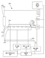
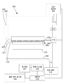
| US10112258B2 (en) * | 2012-03-30 | 2018-10-30 | View, Inc. | Coaxial distance measurement via folding of triangulation sensor optics path |
| US8898928B2 (en) * | 2012-10-11 | 2014-12-02 | Lam Research Corporation | Delamination drying apparatus and method |
-
2012
- 2012-10-11 US US13/650,044 patent/US8898928B2/en not_active Expired - Fee Related
-
2013
- 2013-10-07 SG SG2013075718A patent/SG2013075718A/en unknown
- 2013-10-10 JP JP2013212490A patent/JP6321937B2/ja not_active Expired - Fee Related
- 2013-10-11 CN CN201310473237.7A patent/CN103730332B/zh not_active Expired - Fee Related
- 2013-10-11 KR KR1020130121423A patent/KR20140047009A/ko not_active Ceased
- 2013-10-11 TW TW102136808A patent/TWI602234B/zh not_active IP Right Cessation
Cited By (2)
| Publication number | Priority date | Publication date | Assignee | Title |
|---|---|---|---|---|
| KR20170132676A (ko) * | 2016-05-24 | 2017-12-04 | 가부시키가이샤 스크린 홀딩스 | 기판 처리 장치 및 기판 처리 방법 |
| KR20200056515A (ko) * | 2018-11-14 | 2020-05-25 | 삼성전자주식회사 | 기판 건조 방법, 포토레지스트 현상 방법, 그들을 포함하는 포토리소그래피 방법, 및 기판 건조 장치 |
Also Published As
| Publication number | Publication date |
|---|---|
| US8898928B2 (en) | 2014-12-02 |
| SG2013075718A (en) | 2014-05-29 |
| TWI602234B (zh) | 2017-10-11 |
| CN103730332B (zh) | 2017-05-10 |
| CN103730332A (zh) | 2014-04-16 |
| JP2014090167A (ja) | 2014-05-15 |
| US20140101964A1 (en) | 2014-04-17 |
| TW201430938A (zh) | 2014-08-01 |
| JP6321937B2 (ja) | 2018-05-09 |
Similar Documents
| Publication | Publication Date | Title |
|---|---|---|
| KR20140047009A (ko) | 박리 건조 장치 및 방법 | |
| US9673037B2 (en) | Substrate freeze dry apparatus and method | |
| US9666427B2 (en) | Method of collapse-free drying of high aspect ratio structures | |
| KR102060024B1 (ko) | 레이저 스크라이빙 및 플라즈마 에칭에 의한 디바이스 싱귤레이션을 위한 인-시튜 증착된 마스크 층 | |
| CN109994380A (zh) | 用于在堆叠层中蚀刻特征的方法 | |
| JP2008192643A (ja) | 基板処理装置 | |
| TW201021101A (en) | Method and apparatus for cleaning semiconductor device fabrication equipment using supercritical fluids | |
| US20220139731A1 (en) | Method for treating substrate | |
| US20210272814A1 (en) | Selectively etching for nanowires | |
| US9527118B2 (en) | System and method for treating a substrate | |
| US20210166939A1 (en) | Substrate treating apparatus and substrate treating method | |
| CN101681826B (zh) | 干式蚀刻方法 | |
| TWI745590B (zh) | 蝕刻多孔質膜之方法 | |
| US20140179097A1 (en) | Deposition apparatus and method | |
| JP2009238899A (ja) | 基板処理装置および基板処理方法 | |
| US20230402303A1 (en) | Substrate processing apparatus and substrate processing method | |
| JP2017157714A (ja) | 基板処理装置及び基板処理方法並びに記録媒体 | |
| JP2025525500A (ja) | 窒化ホウ素マスクを使用する炭素ハードマスク開口 | |
| KR20240012439A (ko) | 클리닝 방법 및 플라스마 처리 방법 | |
| JP3120475B2 (ja) | ドライエッチング装置 | |
| JP2007220815A (ja) | プラズマ処理装置およびプラズマ処理方法 | |
| KR20050066113A (ko) | 폴리에처에서의 스트립챔버를 이용한 로드락 챔버부식방지시스템 및 방법 |
Legal Events
| Date | Code | Title | Description |
|---|---|---|---|
| PA0109 | Patent application |
Patent event code: PA01091R01D Comment text: Patent Application Patent event date: 20131011 |
|
| PG1501 | Laying open of application | ||
| PA0201 | Request for examination |
Patent event code: PA02012R01D Patent event date: 20181005 Comment text: Request for Examination of Application Patent event code: PA02011R01I Patent event date: 20131011 Comment text: Patent Application |
|
| E902 | Notification of reason for refusal | ||
| PE0902 | Notice of grounds for rejection |
Comment text: Notification of reason for refusal Patent event date: 20191209 Patent event code: PE09021S01D |
|
| E601 | Decision to refuse application | ||
| PE0601 | Decision on rejection of patent |
Patent event date: 20200213 Comment text: Decision to Refuse Application Patent event code: PE06012S01D Patent event date: 20191209 Comment text: Notification of reason for refusal Patent event code: PE06011S01I |