KR20130114269A - 에스티아이를 위한 실리콘 디옥사이드의 고품질 유전 필름의 제조: 하프 ⅱ― 원격 플라즈마 향상된 증착 공정을 위한 상이한 실록산―기재 전구체의 용도 - Google Patents
에스티아이를 위한 실리콘 디옥사이드의 고품질 유전 필름의 제조: 하프 ⅱ― 원격 플라즈마 향상된 증착 공정을 위한 상이한 실록산―기재 전구체의 용도 Download PDFInfo
- Publication number
- KR20130114269A KR20130114269A KR1020137023298A KR20137023298A KR20130114269A KR 20130114269 A KR20130114269 A KR 20130114269A KR 1020137023298 A KR1020137023298 A KR 1020137023298A KR 20137023298 A KR20137023298 A KR 20137023298A KR 20130114269 A KR20130114269 A KR 20130114269A
- Authority
- KR
- South Korea
- Prior art keywords
- organo
- precursor
- oxygen
- gap
- dielectric material
- Prior art date
Links
- 239000002243 precursor Substances 0.000 title claims abstract description 70
- KPUWHANPEXNPJT-UHFFFAOYSA-N disiloxane Chemical class [SiH3]O[SiH3] KPUWHANPEXNPJT-UHFFFAOYSA-N 0.000 title claims description 10
- 235000012239 silicon dioxide Nutrition 0.000 title claims description 5
- VYPSYNLAJGMNEJ-UHFFFAOYSA-N Silicium dioxide Chemical compound O=[Si]=O VYPSYNLAJGMNEJ-UHFFFAOYSA-N 0.000 title description 26
- 230000015572 biosynthetic process Effects 0.000 title description 9
- 238000005137 deposition process Methods 0.000 title description 4
- 239000000377 silicon dioxide Substances 0.000 title description 4
- 238000000034 method Methods 0.000 claims abstract description 121
- 238000000151 deposition Methods 0.000 claims abstract description 81
- 230000008021 deposition Effects 0.000 claims abstract description 63
- QVGXLLKOCUKJST-UHFFFAOYSA-N atomic oxygen Chemical compound [O] QVGXLLKOCUKJST-UHFFFAOYSA-N 0.000 claims abstract description 57
- 239000012686 silicon precursor Substances 0.000 claims abstract description 57
- 239000003989 dielectric material Substances 0.000 claims abstract description 46
- 239000000758 substrate Substances 0.000 claims abstract description 41
- 229910052760 oxygen Inorganic materials 0.000 claims abstract description 39
- 239000001301 oxygen Substances 0.000 claims abstract description 36
- 238000011049 filling Methods 0.000 claims abstract description 10
- 230000008569 process Effects 0.000 claims description 42
- 239000007789 gas Substances 0.000 claims description 39
- 238000000137 annealing Methods 0.000 claims description 29
- -1 trimethoxysiloxane Chemical compound 0.000 claims description 26
- 239000002253 acid Substances 0.000 claims description 22
- 229910052799 carbon Inorganic materials 0.000 claims description 17
- OKTJSMMVPCPJKN-UHFFFAOYSA-N Carbon Chemical compound [C] OKTJSMMVPCPJKN-UHFFFAOYSA-N 0.000 claims description 16
- XKRFYHLGVUSROY-UHFFFAOYSA-N Argon Chemical compound [Ar] XKRFYHLGVUSROY-UHFFFAOYSA-N 0.000 claims description 12
- LIVNPJMFVYWSIS-UHFFFAOYSA-N silicon monoxide Inorganic materials [Si-]#[O+] LIVNPJMFVYWSIS-UHFFFAOYSA-N 0.000 claims description 11
- 238000005530 etching Methods 0.000 claims description 10
- 239000000463 material Substances 0.000 claims description 9
- MYMOFIZGZYHOMD-UHFFFAOYSA-N Dioxygen Chemical compound O=O MYMOFIZGZYHOMD-UHFFFAOYSA-N 0.000 claims description 8
- 229910001882 dioxygen Inorganic materials 0.000 claims description 8
- 229910052710 silicon Inorganic materials 0.000 claims description 8
- CBENFWSGALASAD-UHFFFAOYSA-N Ozone Chemical compound [O-][O+]=O CBENFWSGALASAD-UHFFFAOYSA-N 0.000 claims description 7
- 229910018557 Si O Inorganic materials 0.000 claims description 6
- 229910052786 argon Inorganic materials 0.000 claims description 6
- CLXMTJZPFVPWAX-UHFFFAOYSA-N trichloro-[dichloro(trichlorosilyloxy)silyl]oxysilane Chemical compound Cl[Si](Cl)(Cl)O[Si](Cl)(Cl)O[Si](Cl)(Cl)Cl CLXMTJZPFVPWAX-UHFFFAOYSA-N 0.000 claims description 6
- XLYOFNOQVPJJNP-UHFFFAOYSA-N water Substances O XLYOFNOQVPJJNP-UHFFFAOYSA-N 0.000 claims description 6
- 229910002808 Si–O–Si Inorganic materials 0.000 claims description 5
- 238000010438 heat treatment Methods 0.000 claims description 5
- 239000000203 mixture Substances 0.000 claims description 5
- MHAJPDPJQMAIIY-UHFFFAOYSA-N Hydrogen peroxide Chemical compound OO MHAJPDPJQMAIIY-UHFFFAOYSA-N 0.000 claims description 4
- POVQBCXZUZAICL-UHFFFAOYSA-N methoxy trimethyl silicate Chemical compound [Si](OC)(OC)(OC)OOC POVQBCXZUZAICL-UHFFFAOYSA-N 0.000 claims description 4
- 239000010703 silicon Substances 0.000 claims description 4
- FDNAPBUWERUEDA-UHFFFAOYSA-N silicon tetrachloride Chemical compound Cl[Si](Cl)(Cl)Cl FDNAPBUWERUEDA-UHFFFAOYSA-N 0.000 claims description 4
- XOAJIYVOSJHEQB-UHFFFAOYSA-N trimethyl trimethoxysilyl silicate Chemical compound CO[Si](OC)(OC)O[Si](OC)(OC)OC XOAJIYVOSJHEQB-UHFFFAOYSA-N 0.000 claims description 4
- MGWGWNFMUOTEHG-UHFFFAOYSA-N 4-(3,5-dimethylphenyl)-1,3-thiazol-2-amine Chemical compound CC1=CC(C)=CC(C=2N=C(N)SC=2)=C1 MGWGWNFMUOTEHG-UHFFFAOYSA-N 0.000 claims description 3
- 229910007991 Si-N Inorganic materials 0.000 claims description 3
- 229910006294 Si—N Inorganic materials 0.000 claims description 3
- JCXJVPUVTGWSNB-UHFFFAOYSA-N nitrogen dioxide Inorganic materials O=[N]=O JCXJVPUVTGWSNB-UHFFFAOYSA-N 0.000 claims description 3
- 125000005843 halogen group Chemical group 0.000 claims description 2
- 125000002496 methyl group Chemical group [H]C([H])([H])* 0.000 claims description 2
- FZHAPNGMFPVSLP-UHFFFAOYSA-N silanamine Chemical compound [SiH3]N FZHAPNGMFPVSLP-UHFFFAOYSA-N 0.000 claims description 2
- 230000001590 oxidative effect Effects 0.000 claims 2
- ICSWLKDKQBNKAY-UHFFFAOYSA-N 1,1,3,3,5,5-hexamethyl-1,3,5-trisilinane Chemical compound C[Si]1(C)C[Si](C)(C)C[Si](C)(C)C1 ICSWLKDKQBNKAY-UHFFFAOYSA-N 0.000 claims 1
- GJLIVGPJMMKPGI-UHFFFAOYSA-N dimethyl bis(trimethoxysilyl) silicate Chemical compound CO[Si](OC)(OC)O[Si](OC)(OC)O[Si](OC)(OC)OC GJLIVGPJMMKPGI-UHFFFAOYSA-N 0.000 claims 1
- RMAQACBXLXPBSY-UHFFFAOYSA-N silicic acid Chemical compound O[Si](O)(O)O RMAQACBXLXPBSY-UHFFFAOYSA-N 0.000 claims 1
- QHAHOIWVGZZELU-UHFFFAOYSA-N trichloro(trichlorosilyloxy)silane Chemical compound Cl[Si](Cl)(Cl)O[Si](Cl)(Cl)Cl QHAHOIWVGZZELU-UHFFFAOYSA-N 0.000 claims 1
- 229910052814 silicon oxide Inorganic materials 0.000 description 19
- 125000003545 alkoxy group Chemical group 0.000 description 13
- 238000002156 mixing Methods 0.000 description 11
- NJPPVKZQTLUDBO-UHFFFAOYSA-N novaluron Chemical compound C1=C(Cl)C(OC(F)(F)C(OC(F)(F)F)F)=CC=C1NC(=O)NC(=O)C1=C(F)C=CC=C1F NJPPVKZQTLUDBO-UHFFFAOYSA-N 0.000 description 11
- 150000003961 organosilicon compounds Chemical class 0.000 description 11
- 150000001875 compounds Chemical class 0.000 description 10
- 238000012545 processing Methods 0.000 description 10
- 238000006243 chemical reaction Methods 0.000 description 9
- 238000009826 distribution Methods 0.000 description 9
- 239000004065 semiconductor Substances 0.000 description 7
- XUIMIQQOPSSXEZ-UHFFFAOYSA-N Silicon Chemical compound [Si] XUIMIQQOPSSXEZ-UHFFFAOYSA-N 0.000 description 6
- 239000012159 carrier gas Substances 0.000 description 6
- 238000010494 dissociation reaction Methods 0.000 description 6
- 230000005593 dissociations Effects 0.000 description 6
- 125000004183 alkoxy alkyl group Chemical group 0.000 description 5
- 125000000217 alkyl group Chemical group 0.000 description 5
- 239000000919 ceramic Substances 0.000 description 5
- 238000004590 computer program Methods 0.000 description 5
- XAGFODPZIPBFFR-UHFFFAOYSA-N aluminium Chemical compound [Al] XAGFODPZIPBFFR-UHFFFAOYSA-N 0.000 description 4
- 238000005229 chemical vapour deposition Methods 0.000 description 4
- 229910052739 hydrogen Inorganic materials 0.000 description 4
- 239000012212 insulator Substances 0.000 description 4
- 229910052751 metal Inorganic materials 0.000 description 4
- 239000002184 metal Substances 0.000 description 4
- LYCAIKOWRPUZTN-UHFFFAOYSA-N Ethylene glycol Chemical compound OCCO LYCAIKOWRPUZTN-UHFFFAOYSA-N 0.000 description 3
- YCKRFDGAMUMZLT-UHFFFAOYSA-N Fluorine atom Chemical compound [F] YCKRFDGAMUMZLT-UHFFFAOYSA-N 0.000 description 3
- OLBVUFHMDRJKTK-UHFFFAOYSA-N [N].[O] Chemical class [N].[O] OLBVUFHMDRJKTK-UHFFFAOYSA-N 0.000 description 3
- 229910052782 aluminium Inorganic materials 0.000 description 3
- 238000005336 cracking Methods 0.000 description 3
- 239000012530 fluid Substances 0.000 description 3
- 229910052731 fluorine Inorganic materials 0.000 description 3
- 239000011737 fluorine Substances 0.000 description 3
- 229910052734 helium Inorganic materials 0.000 description 3
- 239000001307 helium Substances 0.000 description 3
- SWQJXJOGLNCZEY-UHFFFAOYSA-N helium atom Chemical compound [He] SWQJXJOGLNCZEY-UHFFFAOYSA-N 0.000 description 3
- 125000002887 hydroxy group Chemical group [H]O* 0.000 description 3
- 239000012535 impurity Substances 0.000 description 3
- 238000011068 loading method Methods 0.000 description 3
- 238000004519 manufacturing process Methods 0.000 description 3
- 238000000623 plasma-assisted chemical vapour deposition Methods 0.000 description 3
- OBOXTJCIIVUZEN-UHFFFAOYSA-N [C].[O] Chemical class [C].[O] OBOXTJCIIVUZEN-UHFFFAOYSA-N 0.000 description 2
- 238000010521 absorption reaction Methods 0.000 description 2
- VOSJXMPCFODQAR-UHFFFAOYSA-N ac1l3fa4 Chemical compound [SiH3]N([SiH3])[SiH3] VOSJXMPCFODQAR-UHFFFAOYSA-N 0.000 description 2
- 125000003668 acetyloxy group Chemical group [H]C([H])([H])C(=O)O[*] 0.000 description 2
- 150000007513 acids Chemical class 0.000 description 2
- 125000004432 carbon atom Chemical group C* 0.000 description 2
- 238000004891 communication Methods 0.000 description 2
- 238000009833 condensation Methods 0.000 description 2
- 230000005494 condensation Effects 0.000 description 2
- 238000011109 contamination Methods 0.000 description 2
- 125000004122 cyclic group Chemical group 0.000 description 2
- 238000000354 decomposition reaction Methods 0.000 description 2
- 238000013461 design Methods 0.000 description 2
- 239000007788 liquid Substances 0.000 description 2
- QJGQUHMNIGDVPM-UHFFFAOYSA-N nitrogen group Chemical group [N] QJGQUHMNIGDVPM-UHFFFAOYSA-N 0.000 description 2
- 230000003287 optical effect Effects 0.000 description 2
- 229920003209 poly(hydridosilsesquioxane) Polymers 0.000 description 2
- 229920001296 polysiloxane Polymers 0.000 description 2
- 239000000047 product Substances 0.000 description 2
- RHUNFORBKSDWIY-UHFFFAOYSA-N 1,2,3,4,5,6-hexamethoxy-1,2,3,4,5,6-hexamethylhexasilinane Chemical compound CO[Si]1(C)[Si](C)(OC)[Si](C)(OC)[Si](C)(OC)[Si](C)(OC)[Si]1(C)OC RHUNFORBKSDWIY-UHFFFAOYSA-N 0.000 description 1
- LQWNPVJGPXPVNV-UHFFFAOYSA-N 1,4,2,3,5,6-dioxatetrasilinane Chemical compound O1[SiH2][SiH2]O[SiH2][SiH2]1 LQWNPVJGPXPVNV-UHFFFAOYSA-N 0.000 description 1
- KSZFBXOYNRHXCD-UHFFFAOYSA-N 2,2,3,3,5,5,6,6-octamethyl-1,4,2,3,5,6-dioxatetrasilinane Chemical compound C[Si]1(C)O[Si](C)(C)[Si](C)(C)O[Si]1(C)C KSZFBXOYNRHXCD-UHFFFAOYSA-N 0.000 description 1
- QMGHYYDVILNQLH-UHFFFAOYSA-N 2,3,3,4,4,6-hexamethoxyoxazadisilinane Chemical class COC1C[Si](OC)(OC)[Si](OC)(OC)N(OC)O1 QMGHYYDVILNQLH-UHFFFAOYSA-N 0.000 description 1
- DZLQWMNVOBAZGC-UHFFFAOYSA-N 5-methyl-4,6,11-trioxa-1-aza-5-silabicyclo[3.3.3]undecane Chemical compound O1CCN2CCO[Si]1(C)OCC2 DZLQWMNVOBAZGC-UHFFFAOYSA-N 0.000 description 1
- 229910018072 Al 2 O 3 Inorganic materials 0.000 description 1
- CPELXLSAUQHCOX-UHFFFAOYSA-M Bromide Chemical group [Br-] CPELXLSAUQHCOX-UHFFFAOYSA-M 0.000 description 1
- VEXZGXHMUGYJMC-UHFFFAOYSA-M Chloride anion Chemical group [Cl-] VEXZGXHMUGYJMC-UHFFFAOYSA-M 0.000 description 1
- KRHYYFGTRYWZRS-UHFFFAOYSA-M Fluoride anion Chemical group [F-] KRHYYFGTRYWZRS-UHFFFAOYSA-M 0.000 description 1
- 229910018540 Si C Inorganic materials 0.000 description 1
- 229920006362 Teflon® Polymers 0.000 description 1
- ADKPKEZZYOUGBZ-UHFFFAOYSA-N [C].[O].[Si] Chemical compound [C].[O].[Si] ADKPKEZZYOUGBZ-UHFFFAOYSA-N 0.000 description 1
- HMDDXIMCDZRSNE-UHFFFAOYSA-N [C].[Si] Chemical group [C].[Si] HMDDXIMCDZRSNE-UHFFFAOYSA-N 0.000 description 1
- LUXIMSHPDKSEDK-UHFFFAOYSA-N bis(disilanyl)silane Chemical compound [SiH3][SiH2][SiH2][SiH2][SiH3] LUXIMSHPDKSEDK-UHFFFAOYSA-N 0.000 description 1
- GADSHBHCKVKXLO-UHFFFAOYSA-N bis(disilanylsilyl)silane Chemical compound [SiH3][SiH2][SiH2][SiH2][SiH2][SiH2][SiH3] GADSHBHCKVKXLO-UHFFFAOYSA-N 0.000 description 1
- 239000006227 byproduct Substances 0.000 description 1
- 150000001721 carbon Chemical group 0.000 description 1
- 229910010293 ceramic material Inorganic materials 0.000 description 1
- 239000007795 chemical reaction product Substances 0.000 description 1
- 238000004140 cleaning Methods 0.000 description 1
- 239000004020 conductor Substances 0.000 description 1
- 239000000356 contaminant Substances 0.000 description 1
- 238000001816 cooling Methods 0.000 description 1
- 230000001186 cumulative effect Effects 0.000 description 1
- 230000001934 delay Effects 0.000 description 1
- 238000011161 development Methods 0.000 description 1
- LICVGLCXGGVLPA-UHFFFAOYSA-N disilanyl(disilanylsilyl)silane Chemical compound [SiH3][SiH2][SiH2][SiH2][SiH2][SiH3] LICVGLCXGGVLPA-UHFFFAOYSA-N 0.000 description 1
- 230000000694 effects Effects 0.000 description 1
- 238000005516 engineering process Methods 0.000 description 1
- 230000006870 function Effects 0.000 description 1
- 239000011521 glass Substances 0.000 description 1
- 229910052736 halogen Inorganic materials 0.000 description 1
- 150000002367 halogens Chemical class 0.000 description 1
- 239000013529 heat transfer fluid Substances 0.000 description 1
- QOGHHHRYUUFDHI-UHFFFAOYSA-N heptasilepane Chemical compound [SiH2]1[SiH2][SiH2][SiH2][SiH2][SiH2][SiH2]1 QOGHHHRYUUFDHI-UHFFFAOYSA-N 0.000 description 1
- FFUAGWLWBBFQJT-UHFFFAOYSA-N hexamethyldisilazane Chemical compound C[Si](C)(C)N[Si](C)(C)C FFUAGWLWBBFQJT-UHFFFAOYSA-N 0.000 description 1
- GCOJIFYUTTYXOF-UHFFFAOYSA-N hexasilinane Chemical compound [SiH2]1[SiH2][SiH2][SiH2][SiH2][SiH2]1 GCOJIFYUTTYXOF-UHFFFAOYSA-N 0.000 description 1
- 239000001257 hydrogen Substances 0.000 description 1
- 150000002431 hydrogen Chemical class 0.000 description 1
- XMBWDFGMSWQBCA-UHFFFAOYSA-N hydrogen iodide Chemical group I XMBWDFGMSWQBCA-UHFFFAOYSA-N 0.000 description 1
- 239000011261 inert gas Substances 0.000 description 1
- 239000004615 ingredient Substances 0.000 description 1
- 238000003780 insertion Methods 0.000 description 1
- 230000037431 insertion Effects 0.000 description 1
- 239000011810 insulating material Substances 0.000 description 1
- 230000007246 mechanism Effects 0.000 description 1
- OWKFQWAGPHVFRF-UHFFFAOYSA-N n-(diethylaminosilyl)-n-ethylethanamine Chemical class CCN(CC)[SiH2]N(CC)CC OWKFQWAGPHVFRF-UHFFFAOYSA-N 0.000 description 1
- YLZCZVGQEADVNK-UHFFFAOYSA-N n-[chloro-bis(dimethylamino)silyl]-n-methylmethanamine Chemical class CN(C)[Si](Cl)(N(C)C)N(C)C YLZCZVGQEADVNK-UHFFFAOYSA-N 0.000 description 1
- SSCVMVQLICADPI-UHFFFAOYSA-N n-methyl-n-[tris(dimethylamino)silyl]methanamine Chemical compound CN(C)[Si](N(C)C)(N(C)C)N(C)C SSCVMVQLICADPI-UHFFFAOYSA-N 0.000 description 1
- 229910052754 neon Inorganic materials 0.000 description 1
- GKAOGPIIYCISHV-UHFFFAOYSA-N neon atom Chemical compound [Ne] GKAOGPIIYCISHV-UHFFFAOYSA-N 0.000 description 1
- ZGTXAJUQIAYLOM-UHFFFAOYSA-N octasilocane Chemical compound [SiH2]1[SiH2][SiH2][SiH2][SiH2][SiH2][SiH2][SiH2]1 ZGTXAJUQIAYLOM-UHFFFAOYSA-N 0.000 description 1
- 239000003921 oil Substances 0.000 description 1
- 125000001820 oxy group Chemical group [*:1]O[*:2] 0.000 description 1
- 125000004430 oxygen atom Chemical group O* 0.000 description 1
- 230000003071 parasitic effect Effects 0.000 description 1
- CVLHDNLPWKYNNR-UHFFFAOYSA-N pentasilolane Chemical compound [SiH2]1[SiH2][SiH2][SiH2][SiH2]1 CVLHDNLPWKYNNR-UHFFFAOYSA-N 0.000 description 1
- 238000001020 plasma etching Methods 0.000 description 1
- 239000011148 porous material Substances 0.000 description 1
- 239000012713 reactive precursor Substances 0.000 description 1
- 230000004044 response Effects 0.000 description 1
- SCPYDCQAZCOKTP-UHFFFAOYSA-N silanol Chemical compound [SiH3]O SCPYDCQAZCOKTP-UHFFFAOYSA-N 0.000 description 1
- 125000005372 silanol group Chemical group 0.000 description 1
- 229910010271 silicon carbide Inorganic materials 0.000 description 1
- XJKVPKYVPCWHFO-UHFFFAOYSA-N silicon;hydrate Chemical compound O.[Si] XJKVPKYVPCWHFO-UHFFFAOYSA-N 0.000 description 1
- 238000012360 testing method Methods 0.000 description 1
- 238000002207 thermal evaporation Methods 0.000 description 1
- 239000002341 toxic gas Substances 0.000 description 1
- AKYUXYJGXHZKLL-UHFFFAOYSA-N triethoxy(triethoxysilyl)silane Chemical compound CCO[Si](OCC)(OCC)[Si](OCC)(OCC)OCC AKYUXYJGXHZKLL-UHFFFAOYSA-N 0.000 description 1
- LMQGXNPPTQOGDG-UHFFFAOYSA-N trimethoxy(trimethoxysilyl)silane Chemical compound CO[Si](OC)(OC)[Si](OC)(OC)OC LMQGXNPPTQOGDG-UHFFFAOYSA-N 0.000 description 1
- ZQTYRTSKQFQYPQ-UHFFFAOYSA-N trisiloxane Chemical compound [SiH3]O[SiH2]O[SiH3] ZQTYRTSKQFQYPQ-UHFFFAOYSA-N 0.000 description 1
- 238000011144 upstream manufacturing Methods 0.000 description 1
- 238000007740 vapor deposition Methods 0.000 description 1
- 239000011800 void material Substances 0.000 description 1
Images


Classifications
-
- C—CHEMISTRY; METALLURGY
- C23—COATING METALLIC MATERIAL; COATING MATERIAL WITH METALLIC MATERIAL; CHEMICAL SURFACE TREATMENT; DIFFUSION TREATMENT OF METALLIC MATERIAL; COATING BY VACUUM EVAPORATION, BY SPUTTERING, BY ION IMPLANTATION OR BY CHEMICAL VAPOUR DEPOSITION, IN GENERAL; INHIBITING CORROSION OF METALLIC MATERIAL OR INCRUSTATION IN GENERAL
- C23C—COATING METALLIC MATERIAL; COATING MATERIAL WITH METALLIC MATERIAL; SURFACE TREATMENT OF METALLIC MATERIAL BY DIFFUSION INTO THE SURFACE, BY CHEMICAL CONVERSION OR SUBSTITUTION; COATING BY VACUUM EVAPORATION, BY SPUTTERING, BY ION IMPLANTATION OR BY CHEMICAL VAPOUR DEPOSITION, IN GENERAL
- C23C16/00—Chemical coating by decomposition of gaseous compounds, without leaving reaction products of surface material in the coating, i.e. chemical vapour deposition [CVD] processes
- C23C16/06—Chemical coating by decomposition of gaseous compounds, without leaving reaction products of surface material in the coating, i.e. chemical vapour deposition [CVD] processes characterised by the deposition of metallic material
- C23C16/18—Chemical coating by decomposition of gaseous compounds, without leaving reaction products of surface material in the coating, i.e. chemical vapour deposition [CVD] processes characterised by the deposition of metallic material from metallo-organic compounds
-
- C—CHEMISTRY; METALLURGY
- C23—COATING METALLIC MATERIAL; COATING MATERIAL WITH METALLIC MATERIAL; CHEMICAL SURFACE TREATMENT; DIFFUSION TREATMENT OF METALLIC MATERIAL; COATING BY VACUUM EVAPORATION, BY SPUTTERING, BY ION IMPLANTATION OR BY CHEMICAL VAPOUR DEPOSITION, IN GENERAL; INHIBITING CORROSION OF METALLIC MATERIAL OR INCRUSTATION IN GENERAL
- C23C—COATING METALLIC MATERIAL; COATING MATERIAL WITH METALLIC MATERIAL; SURFACE TREATMENT OF METALLIC MATERIAL BY DIFFUSION INTO THE SURFACE, BY CHEMICAL CONVERSION OR SUBSTITUTION; COATING BY VACUUM EVAPORATION, BY SPUTTERING, BY ION IMPLANTATION OR BY CHEMICAL VAPOUR DEPOSITION, IN GENERAL
- C23C16/00—Chemical coating by decomposition of gaseous compounds, without leaving reaction products of surface material in the coating, i.e. chemical vapour deposition [CVD] processes
- C23C16/04—Coating on selected surface areas, e.g. using masks
- C23C16/045—Coating cavities or hollow spaces, e.g. interior of tubes; Infiltration of porous substrates
-
- C—CHEMISTRY; METALLURGY
- C23—COATING METALLIC MATERIAL; COATING MATERIAL WITH METALLIC MATERIAL; CHEMICAL SURFACE TREATMENT; DIFFUSION TREATMENT OF METALLIC MATERIAL; COATING BY VACUUM EVAPORATION, BY SPUTTERING, BY ION IMPLANTATION OR BY CHEMICAL VAPOUR DEPOSITION, IN GENERAL; INHIBITING CORROSION OF METALLIC MATERIAL OR INCRUSTATION IN GENERAL
- C23C—COATING METALLIC MATERIAL; COATING MATERIAL WITH METALLIC MATERIAL; SURFACE TREATMENT OF METALLIC MATERIAL BY DIFFUSION INTO THE SURFACE, BY CHEMICAL CONVERSION OR SUBSTITUTION; COATING BY VACUUM EVAPORATION, BY SPUTTERING, BY ION IMPLANTATION OR BY CHEMICAL VAPOUR DEPOSITION, IN GENERAL
- C23C16/00—Chemical coating by decomposition of gaseous compounds, without leaving reaction products of surface material in the coating, i.e. chemical vapour deposition [CVD] processes
- C23C16/22—Chemical coating by decomposition of gaseous compounds, without leaving reaction products of surface material in the coating, i.e. chemical vapour deposition [CVD] processes characterised by the deposition of inorganic material, other than metallic material
- C23C16/30—Deposition of compounds, mixtures or solid solutions, e.g. borides, carbides, nitrides
- C23C16/40—Oxides
- C23C16/401—Oxides containing silicon
-
- C—CHEMISTRY; METALLURGY
- C23—COATING METALLIC MATERIAL; COATING MATERIAL WITH METALLIC MATERIAL; CHEMICAL SURFACE TREATMENT; DIFFUSION TREATMENT OF METALLIC MATERIAL; COATING BY VACUUM EVAPORATION, BY SPUTTERING, BY ION IMPLANTATION OR BY CHEMICAL VAPOUR DEPOSITION, IN GENERAL; INHIBITING CORROSION OF METALLIC MATERIAL OR INCRUSTATION IN GENERAL
- C23C—COATING METALLIC MATERIAL; COATING MATERIAL WITH METALLIC MATERIAL; SURFACE TREATMENT OF METALLIC MATERIAL BY DIFFUSION INTO THE SURFACE, BY CHEMICAL CONVERSION OR SUBSTITUTION; COATING BY VACUUM EVAPORATION, BY SPUTTERING, BY ION IMPLANTATION OR BY CHEMICAL VAPOUR DEPOSITION, IN GENERAL
- C23C16/00—Chemical coating by decomposition of gaseous compounds, without leaving reaction products of surface material in the coating, i.e. chemical vapour deposition [CVD] processes
- C23C16/44—Chemical coating by decomposition of gaseous compounds, without leaving reaction products of surface material in the coating, i.e. chemical vapour deposition [CVD] processes characterised by the method of coating
- C23C16/448—Chemical coating by decomposition of gaseous compounds, without leaving reaction products of surface material in the coating, i.e. chemical vapour deposition [CVD] processes characterised by the method of coating characterised by the method used for generating reactive gas streams, e.g. by evaporation or sublimation of precursor materials
- C23C16/452—Chemical coating by decomposition of gaseous compounds, without leaving reaction products of surface material in the coating, i.e. chemical vapour deposition [CVD] processes characterised by the method of coating characterised by the method used for generating reactive gas streams, e.g. by evaporation or sublimation of precursor materials by activating reactive gas streams before their introduction into the reaction chamber, e.g. by ionisation or addition of reactive species
-
- C—CHEMISTRY; METALLURGY
- C23—COATING METALLIC MATERIAL; COATING MATERIAL WITH METALLIC MATERIAL; CHEMICAL SURFACE TREATMENT; DIFFUSION TREATMENT OF METALLIC MATERIAL; COATING BY VACUUM EVAPORATION, BY SPUTTERING, BY ION IMPLANTATION OR BY CHEMICAL VAPOUR DEPOSITION, IN GENERAL; INHIBITING CORROSION OF METALLIC MATERIAL OR INCRUSTATION IN GENERAL
- C23C—COATING METALLIC MATERIAL; COATING MATERIAL WITH METALLIC MATERIAL; SURFACE TREATMENT OF METALLIC MATERIAL BY DIFFUSION INTO THE SURFACE, BY CHEMICAL CONVERSION OR SUBSTITUTION; COATING BY VACUUM EVAPORATION, BY SPUTTERING, BY ION IMPLANTATION OR BY CHEMICAL VAPOUR DEPOSITION, IN GENERAL
- C23C16/00—Chemical coating by decomposition of gaseous compounds, without leaving reaction products of surface material in the coating, i.e. chemical vapour deposition [CVD] processes
- C23C16/44—Chemical coating by decomposition of gaseous compounds, without leaving reaction products of surface material in the coating, i.e. chemical vapour deposition [CVD] processes characterised by the method of coating
- C23C16/455—Chemical coating by decomposition of gaseous compounds, without leaving reaction products of surface material in the coating, i.e. chemical vapour deposition [CVD] processes characterised by the method of coating characterised by the method used for introducing gases into reaction chamber or for modifying gas flows in reaction chamber
- C23C16/45523—Pulsed gas flow or change of composition over time
- C23C16/45525—Atomic layer deposition [ALD]
- C23C16/45553—Atomic layer deposition [ALD] characterized by the use of precursors specially adapted for ALD
-
- H—ELECTRICITY
- H01—ELECTRIC ELEMENTS
- H01L—SEMICONDUCTOR DEVICES NOT COVERED BY CLASS H10
- H01L21/00—Processes or apparatus adapted for the manufacture or treatment of semiconductor or solid state devices or of parts thereof
- H01L21/02—Manufacture or treatment of semiconductor devices or of parts thereof
- H01L21/02104—Forming layers
- H01L21/02107—Forming insulating materials on a substrate
- H01L21/02109—Forming insulating materials on a substrate characterised by the type of layer, e.g. type of material, porous/non-porous, pre-cursors, mixtures or laminates
- H01L21/02112—Forming insulating materials on a substrate characterised by the type of layer, e.g. type of material, porous/non-porous, pre-cursors, mixtures or laminates characterised by the material of the layer
- H01L21/02123—Forming insulating materials on a substrate characterised by the type of layer, e.g. type of material, porous/non-porous, pre-cursors, mixtures or laminates characterised by the material of the layer the material containing silicon
- H01L21/02164—Forming insulating materials on a substrate characterised by the type of layer, e.g. type of material, porous/non-porous, pre-cursors, mixtures or laminates characterised by the material of the layer the material containing silicon the material being a silicon oxide, e.g. SiO2
-
- H—ELECTRICITY
- H01—ELECTRIC ELEMENTS
- H01L—SEMICONDUCTOR DEVICES NOT COVERED BY CLASS H10
- H01L21/00—Processes or apparatus adapted for the manufacture or treatment of semiconductor or solid state devices or of parts thereof
- H01L21/02—Manufacture or treatment of semiconductor devices or of parts thereof
- H01L21/02104—Forming layers
- H01L21/02107—Forming insulating materials on a substrate
- H01L21/02109—Forming insulating materials on a substrate characterised by the type of layer, e.g. type of material, porous/non-porous, pre-cursors, mixtures or laminates
- H01L21/022—Forming insulating materials on a substrate characterised by the type of layer, e.g. type of material, porous/non-porous, pre-cursors, mixtures or laminates the layer being a laminate, i.e. composed of sublayers, e.g. stacks of alternating high-k metal oxides
-
- H—ELECTRICITY
- H01—ELECTRIC ELEMENTS
- H01L—SEMICONDUCTOR DEVICES NOT COVERED BY CLASS H10
- H01L21/00—Processes or apparatus adapted for the manufacture or treatment of semiconductor or solid state devices or of parts thereof
- H01L21/02—Manufacture or treatment of semiconductor devices or of parts thereof
- H01L21/02104—Forming layers
- H01L21/02107—Forming insulating materials on a substrate
- H01L21/02109—Forming insulating materials on a substrate characterised by the type of layer, e.g. type of material, porous/non-porous, pre-cursors, mixtures or laminates
- H01L21/02205—Forming insulating materials on a substrate characterised by the type of layer, e.g. type of material, porous/non-porous, pre-cursors, mixtures or laminates the layer being characterised by the precursor material for deposition
- H01L21/02208—Forming insulating materials on a substrate characterised by the type of layer, e.g. type of material, porous/non-porous, pre-cursors, mixtures or laminates the layer being characterised by the precursor material for deposition the precursor containing a compound comprising Si
- H01L21/02214—Forming insulating materials on a substrate characterised by the type of layer, e.g. type of material, porous/non-porous, pre-cursors, mixtures or laminates the layer being characterised by the precursor material for deposition the precursor containing a compound comprising Si the compound comprising silicon and oxygen
- H01L21/02216—Forming insulating materials on a substrate characterised by the type of layer, e.g. type of material, porous/non-porous, pre-cursors, mixtures or laminates the layer being characterised by the precursor material for deposition the precursor containing a compound comprising Si the compound comprising silicon and oxygen the compound being a molecule comprising at least one silicon-oxygen bond and the compound having hydrogen or an organic group attached to the silicon or oxygen, e.g. a siloxane
-
- H—ELECTRICITY
- H01—ELECTRIC ELEMENTS
- H01L—SEMICONDUCTOR DEVICES NOT COVERED BY CLASS H10
- H01L21/00—Processes or apparatus adapted for the manufacture or treatment of semiconductor or solid state devices or of parts thereof
- H01L21/02—Manufacture or treatment of semiconductor devices or of parts thereof
- H01L21/02104—Forming layers
- H01L21/02107—Forming insulating materials on a substrate
- H01L21/02225—Forming insulating materials on a substrate characterised by the process for the formation of the insulating layer
- H01L21/0226—Forming insulating materials on a substrate characterised by the process for the formation of the insulating layer formation by a deposition process
- H01L21/02263—Forming insulating materials on a substrate characterised by the process for the formation of the insulating layer formation by a deposition process deposition from the gas or vapour phase
- H01L21/02271—Forming insulating materials on a substrate characterised by the process for the formation of the insulating layer formation by a deposition process deposition from the gas or vapour phase deposition by decomposition or reaction of gaseous or vapour phase compounds, i.e. chemical vapour deposition
- H01L21/02274—Forming insulating materials on a substrate characterised by the process for the formation of the insulating layer formation by a deposition process deposition from the gas or vapour phase deposition by decomposition or reaction of gaseous or vapour phase compounds, i.e. chemical vapour deposition in the presence of a plasma [PECVD]
-
- H—ELECTRICITY
- H01—ELECTRIC ELEMENTS
- H01L—SEMICONDUCTOR DEVICES NOT COVERED BY CLASS H10
- H01L21/00—Processes or apparatus adapted for the manufacture or treatment of semiconductor or solid state devices or of parts thereof
- H01L21/02—Manufacture or treatment of semiconductor devices or of parts thereof
- H01L21/02104—Forming layers
- H01L21/02107—Forming insulating materials on a substrate
- H01L21/02296—Forming insulating materials on a substrate characterised by the treatment performed before or after the formation of the layer
- H01L21/02318—Forming insulating materials on a substrate characterised by the treatment performed before or after the formation of the layer post-treatment
- H01L21/02337—Forming insulating materials on a substrate characterised by the treatment performed before or after the formation of the layer post-treatment treatment by exposure to a gas or vapour
- H01L21/0234—Forming insulating materials on a substrate characterised by the treatment performed before or after the formation of the layer post-treatment treatment by exposure to a gas or vapour treatment by exposure to a plasma
-
- H—ELECTRICITY
- H01—ELECTRIC ELEMENTS
- H01L—SEMICONDUCTOR DEVICES NOT COVERED BY CLASS H10
- H01L21/00—Processes or apparatus adapted for the manufacture or treatment of semiconductor or solid state devices or of parts thereof
- H01L21/02—Manufacture or treatment of semiconductor devices or of parts thereof
- H01L21/02104—Forming layers
- H01L21/02107—Forming insulating materials on a substrate
- H01L21/02296—Forming insulating materials on a substrate characterised by the treatment performed before or after the formation of the layer
- H01L21/02318—Forming insulating materials on a substrate characterised by the treatment performed before or after the formation of the layer post-treatment
- H01L21/02345—Forming insulating materials on a substrate characterised by the treatment performed before or after the formation of the layer post-treatment treatment by exposure to radiation, e.g. visible light
- H01L21/02348—Forming insulating materials on a substrate characterised by the treatment performed before or after the formation of the layer post-treatment treatment by exposure to radiation, e.g. visible light treatment by exposure to UV light
-
- H—ELECTRICITY
- H01—ELECTRIC ELEMENTS
- H01L—SEMICONDUCTOR DEVICES NOT COVERED BY CLASS H10
- H01L21/00—Processes or apparatus adapted for the manufacture or treatment of semiconductor or solid state devices or of parts thereof
- H01L21/02—Manufacture or treatment of semiconductor devices or of parts thereof
- H01L21/04—Manufacture or treatment of semiconductor devices or of parts thereof the devices having potential barriers, e.g. a PN junction, depletion layer or carrier concentration layer
- H01L21/18—Manufacture or treatment of semiconductor devices or of parts thereof the devices having potential barriers, e.g. a PN junction, depletion layer or carrier concentration layer the devices having semiconductor bodies comprising elements of Group IV of the Periodic Table or AIIIBV compounds with or without impurities, e.g. doping materials
- H01L21/30—Treatment of semiconductor bodies using processes or apparatus not provided for in groups H01L21/20 - H01L21/26
- H01L21/31—Treatment of semiconductor bodies using processes or apparatus not provided for in groups H01L21/20 - H01L21/26 to form insulating layers thereon, e.g. for masking or by using photolithographic techniques; After treatment of these layers; Selection of materials for these layers
- H01L21/3105—After-treatment
- H01L21/311—Etching the insulating layers by chemical or physical means
- H01L21/31105—Etching inorganic layers
- H01L21/31111—Etching inorganic layers by chemical means
- H01L21/31116—Etching inorganic layers by chemical means by dry-etching
-
- H—ELECTRICITY
- H01—ELECTRIC ELEMENTS
- H01L—SEMICONDUCTOR DEVICES NOT COVERED BY CLASS H10
- H01L21/00—Processes or apparatus adapted for the manufacture or treatment of semiconductor or solid state devices or of parts thereof
- H01L21/02—Manufacture or treatment of semiconductor devices or of parts thereof
- H01L21/04—Manufacture or treatment of semiconductor devices or of parts thereof the devices having potential barriers, e.g. a PN junction, depletion layer or carrier concentration layer
- H01L21/18—Manufacture or treatment of semiconductor devices or of parts thereof the devices having potential barriers, e.g. a PN junction, depletion layer or carrier concentration layer the devices having semiconductor bodies comprising elements of Group IV of the Periodic Table or AIIIBV compounds with or without impurities, e.g. doping materials
- H01L21/30—Treatment of semiconductor bodies using processes or apparatus not provided for in groups H01L21/20 - H01L21/26
- H01L21/31—Treatment of semiconductor bodies using processes or apparatus not provided for in groups H01L21/20 - H01L21/26 to form insulating layers thereon, e.g. for masking or by using photolithographic techniques; After treatment of these layers; Selection of materials for these layers
- H01L21/312—Organic layers, e.g. photoresist
- H01L21/3121—Layers comprising organo-silicon compounds
- H01L21/3122—Layers comprising organo-silicon compounds layers comprising polysiloxane compounds
-
- H—ELECTRICITY
- H01—ELECTRIC ELEMENTS
- H01L—SEMICONDUCTOR DEVICES NOT COVERED BY CLASS H10
- H01L21/00—Processes or apparatus adapted for the manufacture or treatment of semiconductor or solid state devices or of parts thereof
- H01L21/02—Manufacture or treatment of semiconductor devices or of parts thereof
- H01L21/04—Manufacture or treatment of semiconductor devices or of parts thereof the devices having potential barriers, e.g. a PN junction, depletion layer or carrier concentration layer
- H01L21/18—Manufacture or treatment of semiconductor devices or of parts thereof the devices having potential barriers, e.g. a PN junction, depletion layer or carrier concentration layer the devices having semiconductor bodies comprising elements of Group IV of the Periodic Table or AIIIBV compounds with or without impurities, e.g. doping materials
- H01L21/30—Treatment of semiconductor bodies using processes or apparatus not provided for in groups H01L21/20 - H01L21/26
- H01L21/31—Treatment of semiconductor bodies using processes or apparatus not provided for in groups H01L21/20 - H01L21/26 to form insulating layers thereon, e.g. for masking or by using photolithographic techniques; After treatment of these layers; Selection of materials for these layers
- H01L21/314—Inorganic layers
- H01L21/316—Inorganic layers composed of oxides or glassy oxides or oxide based glass
- H01L21/31604—Deposition from a gas or vapour
- H01L21/31608—Deposition of SiO2
- H01L21/31612—Deposition of SiO2 on a silicon body
-
- H—ELECTRICITY
- H01—ELECTRIC ELEMENTS
- H01L—SEMICONDUCTOR DEVICES NOT COVERED BY CLASS H10
- H01L21/00—Processes or apparatus adapted for the manufacture or treatment of semiconductor or solid state devices or of parts thereof
- H01L21/02—Manufacture or treatment of semiconductor devices or of parts thereof
- H01L21/04—Manufacture or treatment of semiconductor devices or of parts thereof the devices having potential barriers, e.g. a PN junction, depletion layer or carrier concentration layer
- H01L21/18—Manufacture or treatment of semiconductor devices or of parts thereof the devices having potential barriers, e.g. a PN junction, depletion layer or carrier concentration layer the devices having semiconductor bodies comprising elements of Group IV of the Periodic Table or AIIIBV compounds with or without impurities, e.g. doping materials
- H01L21/30—Treatment of semiconductor bodies using processes or apparatus not provided for in groups H01L21/20 - H01L21/26
- H01L21/31—Treatment of semiconductor bodies using processes or apparatus not provided for in groups H01L21/20 - H01L21/26 to form insulating layers thereon, e.g. for masking or by using photolithographic techniques; After treatment of these layers; Selection of materials for these layers
- H01L21/314—Inorganic layers
- H01L21/316—Inorganic layers composed of oxides or glassy oxides or oxide based glass
- H01L21/31604—Deposition from a gas or vapour
- H01L21/31633—Deposition of carbon doped silicon oxide, e.g. SiOC
-
- H—ELECTRICITY
- H01—ELECTRIC ELEMENTS
- H01L—SEMICONDUCTOR DEVICES NOT COVERED BY CLASS H10
- H01L21/00—Processes or apparatus adapted for the manufacture or treatment of semiconductor or solid state devices or of parts thereof
- H01L21/70—Manufacture or treatment of devices consisting of a plurality of solid state components formed in or on a common substrate or of parts thereof; Manufacture of integrated circuit devices or of parts thereof
- H01L21/71—Manufacture of specific parts of devices defined in group H01L21/70
- H01L21/76—Making of isolation regions between components
- H01L21/762—Dielectric regions, e.g. EPIC dielectric isolation, LOCOS; Trench refilling techniques, SOI technology, use of channel stoppers
- H01L21/76224—Dielectric regions, e.g. EPIC dielectric isolation, LOCOS; Trench refilling techniques, SOI technology, use of channel stoppers using trench refilling with dielectric materials
-
- H—ELECTRICITY
- H01—ELECTRIC ELEMENTS
- H01L—SEMICONDUCTOR DEVICES NOT COVERED BY CLASS H10
- H01L21/00—Processes or apparatus adapted for the manufacture or treatment of semiconductor or solid state devices or of parts thereof
- H01L21/02—Manufacture or treatment of semiconductor devices or of parts thereof
- H01L21/02104—Forming layers
- H01L21/02107—Forming insulating materials on a substrate
- H01L21/02109—Forming insulating materials on a substrate characterised by the type of layer, e.g. type of material, porous/non-porous, pre-cursors, mixtures or laminates
- H01L21/02112—Forming insulating materials on a substrate characterised by the type of layer, e.g. type of material, porous/non-porous, pre-cursors, mixtures or laminates characterised by the material of the layer
- H01L21/02123—Forming insulating materials on a substrate characterised by the type of layer, e.g. type of material, porous/non-porous, pre-cursors, mixtures or laminates characterised by the material of the layer the material containing silicon
- H01L21/02126—Forming insulating materials on a substrate characterised by the type of layer, e.g. type of material, porous/non-porous, pre-cursors, mixtures or laminates characterised by the material of the layer the material containing silicon the material containing Si, O, and at least one of H, N, C, F, or other non-metal elements, e.g. SiOC, SiOC:H or SiONC
-
- H—ELECTRICITY
- H01—ELECTRIC ELEMENTS
- H01L—SEMICONDUCTOR DEVICES NOT COVERED BY CLASS H10
- H01L21/00—Processes or apparatus adapted for the manufacture or treatment of semiconductor or solid state devices or of parts thereof
- H01L21/02—Manufacture or treatment of semiconductor devices or of parts thereof
- H01L21/02104—Forming layers
- H01L21/02107—Forming insulating materials on a substrate
- H01L21/02109—Forming insulating materials on a substrate characterised by the type of layer, e.g. type of material, porous/non-porous, pre-cursors, mixtures or laminates
- H01L21/02205—Forming insulating materials on a substrate characterised by the type of layer, e.g. type of material, porous/non-porous, pre-cursors, mixtures or laminates the layer being characterised by the precursor material for deposition
- H01L21/02208—Forming insulating materials on a substrate characterised by the type of layer, e.g. type of material, porous/non-porous, pre-cursors, mixtures or laminates the layer being characterised by the precursor material for deposition the precursor containing a compound comprising Si
- H01L21/02211—Forming insulating materials on a substrate characterised by the type of layer, e.g. type of material, porous/non-porous, pre-cursors, mixtures or laminates the layer being characterised by the precursor material for deposition the precursor containing a compound comprising Si the compound being a silane, e.g. disilane, methylsilane or chlorosilane
-
- H—ELECTRICITY
- H01—ELECTRIC ELEMENTS
- H01L—SEMICONDUCTOR DEVICES NOT COVERED BY CLASS H10
- H01L21/00—Processes or apparatus adapted for the manufacture or treatment of semiconductor or solid state devices or of parts thereof
- H01L21/02—Manufacture or treatment of semiconductor devices or of parts thereof
- H01L21/02104—Forming layers
- H01L21/02107—Forming insulating materials on a substrate
- H01L21/02225—Forming insulating materials on a substrate characterised by the process for the formation of the insulating layer
- H01L21/0226—Forming insulating materials on a substrate characterised by the process for the formation of the insulating layer formation by a deposition process
- H01L21/02263—Forming insulating materials on a substrate characterised by the process for the formation of the insulating layer formation by a deposition process deposition from the gas or vapour phase
- H01L21/02271—Forming insulating materials on a substrate characterised by the process for the formation of the insulating layer formation by a deposition process deposition from the gas or vapour phase deposition by decomposition or reaction of gaseous or vapour phase compounds, i.e. chemical vapour deposition
- H01L21/0228—Forming insulating materials on a substrate characterised by the process for the formation of the insulating layer formation by a deposition process deposition from the gas or vapour phase deposition by decomposition or reaction of gaseous or vapour phase compounds, i.e. chemical vapour deposition deposition by cyclic CVD, e.g. ALD, ALE, pulsed CVD
-
- Y—GENERAL TAGGING OF NEW TECHNOLOGICAL DEVELOPMENTS; GENERAL TAGGING OF CROSS-SECTIONAL TECHNOLOGIES SPANNING OVER SEVERAL SECTIONS OF THE IPC; TECHNICAL SUBJECTS COVERED BY FORMER USPC CROSS-REFERENCE ART COLLECTIONS [XRACs] AND DIGESTS
- Y10—TECHNICAL SUBJECTS COVERED BY FORMER USPC
- Y10S—TECHNICAL SUBJECTS COVERED BY FORMER USPC CROSS-REFERENCE ART COLLECTIONS [XRACs] AND DIGESTS
- Y10S438/00—Semiconductor device manufacturing: process
- Y10S438/931—Silicon carbide semiconductor
Landscapes
- Chemical & Material Sciences (AREA)
- Engineering & Computer Science (AREA)
- Physics & Mathematics (AREA)
- Microelectronics & Electronic Packaging (AREA)
- Power Engineering (AREA)
- Condensed Matter Physics & Semiconductors (AREA)
- General Physics & Mathematics (AREA)
- Manufacturing & Machinery (AREA)
- Computer Hardware Design (AREA)
- Chemical Kinetics & Catalysis (AREA)
- General Chemical & Material Sciences (AREA)
- Organic Chemistry (AREA)
- Materials Engineering (AREA)
- Mechanical Engineering (AREA)
- Metallurgy (AREA)
- Inorganic Chemistry (AREA)
- Plasma & Fusion (AREA)
- Spectroscopy & Molecular Physics (AREA)
- Formation Of Insulating Films (AREA)
- Chemical Vapour Deposition (AREA)
- Silicon Polymers (AREA)
- Element Separation (AREA)
Abstract
기판 상에 형성된 갭 내에 유전층을 증착시키는 방법이 기재된다. 그러한 방법은 유기-실리콘 전구체와 산소 전구체를 증착 챔버에 도입하는 것을 포함한다. 유기-실리콘 전구체는 8 미만의 C:Si 원자 비율을 지니며, 산소 전구체는 증착 챔버의 외부에서 생성되는 원자 산소를 포함한다. 전구체는 반응하여 갭 내에 유전층을 형성시킨다. 또한 갭을 유전 재료로 충전하는 방법이 기재된다. 이러한 방법은 8 미만의 C:Si 원자 비율을 지니는 유기-실리콘 전구체 및 산소 전구체를 제공하고, 전구체들로부터 플라즈마를 형성시켜서 갭 내에 유전 재료의 제 1 부분을 증착시키는 것을 포함한다. 유전 재료는 에칭될 수 있으며, 유전 재료의 제 2 부분이 갭 내에 형성될 수 있다. 유전 재료의 제 1 부분 및 제 2 부분은 어닐링될 수 있다.
Description
본 발명은 기판 상에 형성된 갭 내에 유전층을 증착시키는 방법에 관한 것이다.
또한, 본 발명은 갭을 유전 재료로 충전시키는 방법을 포함한다.
또한, 본 발명은 추가로 기판상의 갭 내에 유전 재료를 증착시키고 어닐링하는 방법에 관한 것이다.
관련 출원의 상호-참조
본 출원은 2006년 5월 30일자로 출원되고 발명의 명칭이 "실리콘 함유 전구체 및 원자 산소를 사용한 고품질 유동형 실리콘 디옥사이드의 화학적 기상 증착(CHEMICAL VAPOR DEPOSITION OF HIGH QUALITY FLOW-LIKE SILICON DIOXIDE USING A SILICON CONTAINING PRECURSOR AND ATOMIC OXYGEN)"인 잉글 등(Ingle et al)에 공동 양도된 미국가특허출원 제60/803,493호와 관련되어 있다. 본 출원은 또한 2006년 5월 30일자로 출원되고 발명의 명칭이 "실리콘 디옥사이드의 필름 품질을 향상시키기 위한 신규 증착-플라즈마 경화 사이클 공정(A NOVEL DEPOSITION-PLASMA CURE CYCLE PROCESS TO ENHANCE FILM QUALITY OF SILICON DIOXIDE)"인 첸 등(Chen et al)에 공동 양도된 미국가특허출원 제60/803,481호와 관련되어 있다. 본 출원은 추가로 2006년 5월 30일자로 출원되고 발명의 명칭이 "갭충전 및 정각 필름 적용을 위한 저유전 상수 필름을 증착 및 경화하는 방법(A METHOD FOR DEPOSITING AND CURING LOW-K FILMS FOR GAPFILL AND CONFORMAL FILM APPLICATIONS)"인 문로 등(Munro et al)에 공동 양도된 미국가특허출원 제60/803,489호와 관련되어 있다. 본 출원은 또한 추가로 2006년 6월 22일자로 출원되고 발명의 명칭이 "상향식 갭충전을 위한 유전 증착 및 에치백 공정(DIELECTRIC DEPOSITION AND ETCH BACK PROCESSES FOR BOTTOM UP GAP FILL)"인 루보미르스키(Lubomirsky)에 공동 양도된 미국가특허출원 제60/805,573호와 관련되어 있다. 상기 4 개의 관련 출원의 전체 내용이 모든 목적을 위해 본원에서 참조로 통합된다.
발명의 배경
반도체 디바이스의 기하학적 형태는 수십년 전 이들이 소개된 이래로 그 크기가 극적으로 감소하고 있다. 현대의 반도체 제조 장치는 통상적으로 250nm, 180nm, 및 65nm 피처 크기(feature size)의 디바이스를 생산하고 있으며, 훨씬 더 작은 기하학적 형태를 지니는 디바이스를 제조하기 위한 새로운 장치가 개발되고 실행되고 있다. 그러나, 더 작은 크기는 크로스토크(cross-talk) 및 유도 용량(parasitic capacitance)을 포함한 전기적 간섭의 기회를 증가시킬 수 있는 디바이스 엘리먼트들이 함께 더 가깝게 작동해야 함을 의미한다.
전기적 간섭도를 감소시키기 위해서, 유전 절연 재료가 갭, 트렌치(trench), 및 디바이스 엘리먼트들, 금속 라인들, 및 그 밖의 디바이스 피처들 사이의 그 밖의 공간들을 충전시키는데 사용된다. 디바이스 피처들 사이의 공간에서의 형성의 용이성 및 낮은 유전 상수(즉, "k-값")를 위한 유전 재료가 선택된다. 낮은 k-값을 지니는 유전체는 크로스-토크 및 RC 시간 지연을 최소화시키는데 뿐만 아니라 디바이스의 전체 전력 소모를 감소시키는데 더욱 좋다. 통상의 유전 재료는 실리콘 옥사이드를 포함하며, 이러한 실리콘 옥사이드는 통상의 CVD 기술로 증착되는 경우 4.0 내지 4.2의 평균 k-값을 지닌다.
통상의 CVD 실리콘 옥사이드의 k-값이 많은 디바이스 구조에 허용되지만, 끊임없는 크기 감소 및 디바이스 엘리먼트의 밀도 증가가 반도체 제조자들로 하여금 계속해서 낮은 k-값을 지니는 유전 재료를 찾게 하고 있다. 한 가지 방법은 실리콘 옥사이드를 불소로 도핑시켜서 유전상수가 약 3.4 내지 3.6 만큼 낮은 불소-도핑된 실리콘 옥사이드 필름(즉, "FSG" 필름)을 제조하는 것이었다. 또 다른 방법은 기판을 하이드로겐 실세스퀴옥산(hydrogen silsesquioxane (HSQ))과 같은 고유동성 전구체로 코팅하여 다공성 저-k 필름을 형성시키는 스핀-온 글래스 기술(spin-on glass technique)의 개발이었다.
더욱 최근에는, k-값이 3.0 또는 그 미만인 실리콘-산소-탄소(Si-O-C) 필름이 개발되었다. 이들 저-k 필름은 종종 기판상의 탄소-실리콘 및 산소 전구체의 화학적 기상 증착에 의해서 증착된다. 이들 Si-O-C 필름은 순수한 및 불소-도핑된 실리콘 옥사이드 필름 보다 낮은 k-값을 지니지만, 이들은 또한 실질적으로 더 다공성인 경향이 있으며, 이는 부정적인 결과를 나타낼 수 있다. 다공성 필름은 물의 흡수가 증가하기 쉬우며, 이는 필름의 k-값을 증가시킬 수 있다. 다공성 필름은 또한 필름을 더욱 부식 및 응력 균열(stress cracking)되게 할 수 있는 더 높은 "습식 에치 속도 비(wet etch rate ratios(WERRs))"를 지닌다. 따라서, 다공도가 감소되고, WERR 값이 더 낮고 균열이 덜한 저-k 탄소 기재 필름을 증착시키는 새로운 방법이 요구되고 있다. 이들 및 그 밖의 문제는 본 발명의 구체예에 의해서 극복된다.
발명의 간단한 요약
본 발명의 구체예는 기판 상에 형성된 갭 내에 유전층을 증착시키는 방법을 포함한다. 이러한 방법은 유기-실리콘 전구체 및 산소 전구체를 증착 챔버에 도입하는 단계를 포함할 수 있다. 유기-실리콘 전구체는 8 미만의 C:Si 원자 비율을 지닐 수 있으며, 산소 전구체는 증착 챔버의 외부에서 생성되는 원자 산소(atomic oxygen)를 포함할 수 있다. 그러한 방법은 또한 전구체들을 반응시켜 갭 내에 유전층을 형성시키는 것을 포함할 수 있다.
본 발명의 구체예는 또한 갭을 유전 재료로 충전시키는 방법을 포함한다. 그러한 방법은 유기-실리콘 전구체 및 산소 전구체를 증착 챔버에 제공하는 단계를 포함할 수 있으며, 여기서, 유기-실리콘 전구체는 8 미만의 C:Si 원자 비율을 지닌다. 플라즈마는 증착 챔버 내에서 전구체로부터 생성될 수 있으며, 여기서 그러한 플라즈마는 갭 내에 유전 재료의 제 1 부분을 증착시킨다. 그러한 방법은 또한 유전 재료의 제 1 부분을 에칭시켜서 재료중의 탄소 함량을 감소시키고, 갭 내에 유전 재료의 제 2 부분을 증착시키는 것을 포함할 수 있다. 갭 내의 유전 재료의 제 1 및 제 2 부분은 어닐링될 수 있다.
본 발명의 구체예는 추가로 기판 상의 갭 내에 유전 재료를 증착시키고 어닐링하는 방법을 포함한다. 그러한 방법은 유기-실리콘 전구체와 산소 전구체를 증착 챔버에 제공하는 단계를 포함할 수 있으며, 여기서, 그러한 유기-실리콘 전구체는 8 미만의 C:Si 원자 비율을 지닌다. 전구체들은 반응하여 갭 내에 유전 재료를 증착시키며, 열적 어닐링이 증착된 유전 재료에 대해서 수행될 수 있다. 게다가, 플라즈마 어닐링이 또한 증착된 유전 재료에 대해서 수행될 수 있다.
추가의 구체예 및 특징이 이하 설명부분에 일부 기재되어 있으며, 일부는 명세서를 시험하는 경우 당업자에게는 자명하게 되거나 본 발명을 실시함에 의해서 이해될 수 있다. 본 발명의 이러한 특징 및 이점은 본원에 기재된 도구, 조합 및 방법에 의해서 실현되고 얻어질 수 있다.
기판의 표면 상에 및 갭 내에 유전 재료를 증착시키는 시스템 및 방법이 기재되어 있다. 유전 재료는 통상의 테트라에톡시실록산(tetraethoxysiloxane (TEOS)) 보다 낮은 탄소 원자 대 실리콘 원자 비율(C:Si 비율)을 지니는 유기-실리콘 화합물로부터 형성될 수 있다. 이들 화합물을 산소 전구체와 조합함으로써 형성되는 유전 필름은 전형적으로는 초기 증착된 TEOS 기재 실리콘 옥사이드 보다 낮은 탄소 함량, 낮은 다공도 및 낮은 WERRs를 지닌다. 이러한 구성은 필름이 TEOS 기재 옥사이드 필름에 비해서 균열, 공극 형성, 수분 흡수 및/또는 수축에 덜 민감하게 한다.
유기-실리콘 화합물은 또한 TEOS O:Si 비율과 동일하거나 더 큰 산소 원자 대 실리콘 원자 비율(O:Si 비율)을 지닐 수 있다. 낮은 C:Si 비율 및 높은 O:Si 비율을 지니는 유기-실리콘 전구체는 실리콘 전구체로서 TEOS만을 사용하는 통상적으로 제조된 옥사이드에 비해서 더 낮은 탄소 함량을 지니는 더 높은 품질의 실리콘 옥사이드 필름을 생성시킨다. 구체예는 또한 분자 구조에 하나 이상의 Si-O-Si 연결을 지니는 유기-실리콘 전구체를 포함한다. Si 전구체 중의 이러한 연결은 탄소 및 히드록실기로부터의 오염이 감소된 SiOx 필름의 형성을 용이하게 한다.
유기-실리콘 화합물은 또한 Si-O기로 용이하게 산화될 수 있는 할로겐 및 질소 기를 포함하는 할로겐화된 실록산 및 실라족산을 포함할 수 있다. 할로겐화된 실록산은 염소화된 실록산, 예컨대, Si-C기가 분자 산소, 오존, 이산화질소, 과산화수소 등에 의해서 탄소 수준이 감소된 Si-O기로 용이하게 산화될 수 있는 옥타클로로트리실록산(octachlorotrisiloxane (OCTS))을 포함할 수 있다. 유사하게는, 실라족산, 예컨대, 헥사메톡시디실라족산(hexamethoxydisilazoxanes (HMDS-H))은 Si-O기로 용이하게 산화될 수 있는 Si-N기를 지닌다.
유기-실리콘 화합물은 증착 챔버 중의 반응성 원자 산소 전구체에 도입되어, 증착된 유전 필름 중의 Si-O기의 형성을 더 증가시킬 수 있다. 원자 산소는, 증착 챔버로 보내져서 유기-실리콘 전구체와 반응되기 전에, 예를 들어, 원격 고밀도 플라즈마 생성 유닛을 사용함으로써 증착 챔버 외부에서 초기에 생성될 수 있다. 생성되는 실리콘 옥사이드 층은, 증착 챔버 내에서 유기-실리콘 전구체를 분자 산소, 오존 등과 반응시킴으로써 형성된 통상의 옥사이드 필름 보다 개선된 유동성 및 갭-흐름 특성 및 더 낮은 탄소 함량 및 다공성을 가질 수 있다. 본 발명의 방법, 생성물 및 시스템의 구체예에 대한 추가의 상세사항이 이하 기재될 것이다.
예시적인 유전 증착 방법
도 1은 본 발명의 구체예에 따른 유전 증착의 단순 개요를 포함하는 플로우챠트를 나타낸다. 도시된 방법(100)은 유기-실리콘 전구체(102) 및 산소 전구체(104)를 증착 챔버에 도입하는 것을 포함한다. 전구체들은 챔버 내에서 반응하여 기판(106)의 표면 상에 및 갭 내에 유전층을 형성시킨다.
증착 챔버에 도입된 유기-실리콘 전구체는 8 미만의 C:Si 원자 비율(예, 7, 6, 5, 4, 3, 2, 또는 1 또는 그 미만의 C:Si 비율)을 지닐 수 있다. 이는 유기-실리콘 전구체 분자 내에서, 존재하는 각각의 실리콘 원자에 대해 8개 보다 적은 탄소 원자가 존재함을 의미한다. 비교해 보면, 이하 나타낸 테트라에톡시실록산(TEOS) 분자는 각각의 실리콘 원자에 대해 8개의 탄소 원자(즉, 8의 C:Si 비율)를 지닌다:

유기-실리콘 전구체는 실록산 화합물, 예컨대, 다른 실록산 화합물 중에서도, 트리에톡시실록산(TRIES), 테트라메톡시실록산(TMOS), 트리메톡시실록산(TRIMOS), 헥사메톡시디실록산(HMODS), 옥타메톡시트리실록산(OMOTS), 및/또는 옥타메톡시도데카실록산(OMODDS)일 수 있다:

유기-실리콘 화합물은 또한 하나 이상의 질소기를 포함하는 실라족산 화합물일 수 있다. 실라족산 화합물은, 다른 실라족산 화합물 중에서도, 헥사메톡시디실라족산 (HMDS-H), 메틸 헥사메톡시디실라족산 (HMDS-CH3), 클로로헥사메톡시디실라족산 (HMDS-Cl), 헥사에톡시디실라족산(HEDS-H), 노나메톡시트리실라족산 (NMTS), 및 옥타메톡시시클릭실라족산 (OMCS)을 포함할 수 있다:

유기-실리콘 화합물은 추가로 하나 이상의 할로겐 기(예컨대, 플루오라이드, 클로라이드, 브로마이드, 또는 아이오다이드 기)를 포함하는 할로겐화된 실록산 화합물이다. 예를 들어, 할로겐화된 실록산은, 염소화된 실록산 화합물, 예컨대, 다른 염소화된 실록산 화합물 중에서도, 테트라클로로실란 (TECS), 디클로로디에톡시실록산 (DCDES), 클로로트리에톡시실록산(CTES), 헥사클로로디실록산 (HCDS), 및/또는 옥타클로로트리실록산 (OCTS)일 수 있다:

유기-실리콘 화합물은 또한 약 O, 0.5, 1, 2, 3, 4, 5, 6 등 또는 그 초과의 O:Si 비율을 지닐 수 있다. 예를 들어, TMOS는 4의 O:Si 원자 비율(TEOS와 동일)을 지닌다. 그 밖의 유기-실리콘 화합물, 예컨대, TRIES, 및 TRIMOS는 3의 O:Si 비율을 지닌다. 다른 화합물, 예컨대, HCDS는 0.5의 O:Si 비율을 지니며, TECS는 0의 O:Si 비율을 지닌다.
유기-실리콘 전구체는, 다른 유기-실리콘 화합물 중에서도, HMODS, OMOTS, OMODDS, HCDS, 및 OCTS에서 나타낸 바와 같이, Si-O-Si 연결을 추가로 포함할 수 있다. Si 전구체에서의 이러한 연결은 탄소 및 히드록실기로부터의 오염이 감소된 SiOx 필름의 형성을 촉진시킬 수 있다.
유기-실리콘 전구체는 추가로, 다른 화합물 중에서도, 아미노실란, 예컨대, 트리실릴아민(TSA), 헥사메틸디실라잔 (HMDS), 실라트란, 테트라키스(디메틸아미노)실란, 비스(디에틸아미노)실란, 트리스(디메틸아미노)클로로실란, 및 메틸실라트란을 포함할 수 있다:

유기-실리콘 전구체는 또한 추가로 알콕시 디실란, 알콕시-알킬 디실란, 및 알콕시-아세톡시 디실란을 포함한 디실란을 포함할 수 있다. 알콕시 디실란은 하기 화합물을 포함할 수 있다:

상기 식에서,
R1 -6은 독립적으로 C1 -3 알킬옥시기일 수 있다. 예를 들어, 알콕시 디실란은, 다른 알콕시 디실란 중에서도, 헥사메톡시디실란, 및 헥사에톡시디실란을 포함할 수 있다.
알콕시 디실란은 또한 Si 부분에 결합된 알콕시기를 지닌 시클릭 디실란 화합물을 포함할 수 있다. 예를 들어, 알콕시시클로실란은, 다른 것들 중에서도, 옥타에톡시시클로부타실란, 데카부타옥시시클로펜타실란, 및 도데카메톡시시클로헥사실란을 포함할 수 있다. 알콕시 디실란의 일부예는 하기된 바와 같다:

알콕시-알킬 디실란은 하기 화합물을 포함할 수 있다:

상기 식에서, R7 -12는 독립적으로 C1 -3 알킬기 또는 C1 -3 알킬옥시기일 수 있으며, R7 -12중 하나 이상은 알킬기이고, R7 -12중 하나 이상은 알킬옥시기이다. 알콕시-알킬 디실란은 또한 알킬 및 알콕시 부분을 지닌 시클릭 디실란, 예컨대, 결합된 하나 이상의 알킬 및 알콕시를 지니는 부타실란, 펜타실란, 헥사실란, 헵타실란, 옥타실란 등을 포함할 수 있다. 그러한 예에는, 다른 알콕시-알킬 시클로실란 중에서도, 옥타메틸-1,4-디옥사-2,3,5,6-테트라실라시클로헥산; 1,4-디옥사-2,3,5,6-테트라실라시클로헥산; 및 1,2,3,4,5,6-헥사메톡시-1,2,3,4,5,6-헥사메틸시클로헥사실란을 포함한다. 알콕시-알킬 디실란의 일부 예는 다음과 같다:

알콕시-아세톡시 디실란은 하기 화합물을 포함할 수 있다:

상기 식에서, R13 -17은 독립적으로 C1 -3 알킬기, C1 -3 알콕시기 또는 아세톡시기일 수 있으며, R13 -17 중 하나 이상은 알콕시기이고, R13 -17 중 하나 이상은 아세톡시기이다.
유기-실리콘 전구체는 또한 추가로 유기시클로실란, 예컨대, 시클로부타실란, 시클로펜타실란, 시클로헥사실란, 시클로헵타실란, 시클로옥타실란 등을 포함할 수 있다.
산소 전구체는 분자 산소(O2), 오존(O3), 질소-산소 화합물(예컨대, NO, NO2, N2O 등), 수소-산소 화합물(예컨대, H2O, H2O2 등), 및 그 밖의 산소 함유 전구체 및 이들 전구체의 조합물을 포함할 수 있다. 일부 구체예에서, 산소 전구체는 원격적으로 생산되고 유기-실리콘 전구체와 함께 증착 챔버 내로 도입되는 원자 산소 라디칼을 포함할 수 있다.
이제 도 2를 참조하면, 본 발명의 구체예에 따른 유전 재료로 갭을 충전시키는 방법(200)을 예시하는 플로우챠트가 도시되어 있다. 방법(200)은 기판을 증착 챔버에 제공하고, 이어서 유기-실리콘 전구체(202) 및 산소 전구체(204)를 챔버에 도입하는 것을 포함할 수 있다. 기판은 반도체 웨이퍼(예컨대, 200mm, 300mm, 400mm 등의 실리콘 웨이퍼)일 수 있으며, 이전의 공정에서 형성된 구조물, 디바이스 성분 등을 포함할 수 있다. 예를 들어, 기판은 높은 높이 대 폭 종횡비(aspect raio)(예컨대, 5:1 또는 그 초과, 6:1 또는 그 초과, 7:1 또는 그 초과, 8:1 또는 그 초과, 9:1 또는 그 초과, 10:1 또는 그 초과, 11:1 또는 그 초과, 12:1 또는 그 초과 등)를 갖는 갭, 트렌치 등을 포함할 수 있다. 유전 재료는 기판의 갭 내 및 다른 표면에 증착된다.
상기 주지된 바와 같이, 유기-실리콘 전구체는 실록산, 할로겐화된 실록산, 및/또는 실라족산 화합물을 포함할 수 있으며, 8 미만의 C:Si 원자 비율의 유기-실리콘 화합물을 포함할 수 있다. 실리콘 전구체는 증착 챔버에 도입 전에 또는 도입 동안에 캐리어 가스와 혼합될 수 있다. 캐리어 가스는 기판 상의 옥사이드 필름의 형성을 과도하게 방해하지 않는 불활성 가스일 수 있다. 캐리어 가스의 예는, 다른 가스 중에서도, 헬륨, 네온, 아르곤, 및 수소(H2)를 포함한다.
예를 들어, 유기-실리콘 전구체는 유기-실리콘 화합물(가스 또는 액체)을 헬륨과 혼합함으로써 약 600 내지 약 2400 sccm의 유량으로 실온 유기-실리콘 전구체를 통해서 증착 챔버에 도입되어 챔버에 약 800 내지 약 1600mgm 속도의 전구체 흐름을 제공할 수 있다.
산소 전구체는 분자 산소(O2), 오존(O3), 질소-산소 화합물(예컨대, NO, NO2, N2O 등), 수소-산소 화합물(예컨대, H2O, H2O2 등), 탄소-산소 화합물(예컨대, CO, CO2 등), 및 다른 산소 함유 전구체 및 이러한 전구체의 조합을 포함할 수 있다. 방법(300)에 대해서 이하 상세히 기재된 바와 같이, 산소 전구체는 또한 원격적으로 생산되고 유기-실리콘 전구체와 함께 증착 챔버 내로 도입되는 원자 산소 라디칼을 포함할 수 있다.
방법(200)은 전구체로부터 증착 챔버 내에서 플라즈마를 생성시키고, 유전 재료(206)의 제 1 부분을 형성시키는 것을 포함한다. 방법(200)의 구체예에서, 산소 및 유기-실리콘 전구체는 증착 챔버에 도입되기 전에 혼합되지 않는다. 전구체는 반응 챔버 둘레에 분포된 공간적으로 분리된 전구체 유입구를 통해서 챔버에 유입될 수 있다. 예를 들어, 산소 전구체는 챔버의 상부에 있는 유입구(또는 유입구들)로부터 유입될 수 있으며, 기판 위에 직접적으로 정위될 수 있다. 유입구는 산소 전구체의 흐름을 기판 증착 표면에 수직인 방향으로 유도한다. 한편, 실리콘 전구체가 증착 챔버 측면 둘레에 있는 하나 이상의 유입구로부터 유입될 수 있다. 유입구는 실리콘 전구체의 흐름을 증착 표면에 대체로 평행한 방향으로 유도할 수 있다.
산소와 유기-실리콘 플라즈마가 증착 챔버 내에서 반응함에 따라서, 이는 기판 증착 표면 상의 실리콘 옥사이드 유전층의 제 1 부분을 형성한다. 초기 옥사이드 층은 우수한 유동성을 지니며, 증착 표면에 존재하는 구조물 내의 갭, 트렌치, 공극, 시임(seam) 등으로 신속하게 이동할 수 있다. 이는 방법(200)이 높은 높이 대 폭 종횡비(예컨대, 약 5:1, 6:1, 7:1, 8:1, 9:1, 10:1, 11:1, 및 12:1 또는 그 초과의 종횡비(ARs))를 지니는 갭, 트렌치, 및 그 밖의 표면 구조물 내의 공극 및 시임이 실질적으로 없는 옥사이드 충전을 제공하게 한다.
유전 재료의 제 1 부분이 형성된 후에, 챔버 내로의 전구체의 흐름은 중단될 수 있고, 재료는 에칭(208)될 수 있다. 에칭 단계는 재료 중의 불순물을 해리시키고 제거하는데 이용될 수 있으며, 또한 재료를 평탄화시키는데 이용될 수 있다. 에칭 공정은 단일-스텝 에치(single-step etch), 또는 멀티스텝 에치를 포함할 수 있다. 멀티스텝 에치 공정은 저-밀도 플라즈마를 이용하여 더 큰 유기분자를 해리시키고 유전 재료 중의 탄소의 적어도 일부를 제거하는 제 1 에치를 포함할 수 있다. 이러한 저-밀도 플라즈마 에치는 RPS 시스템을 사용하여 옥사이드 층을 에칭하는 Ar/O2 플라즈마를 생성시키는 것을 포함할 수 있다. 에칭 조건은, 예를 들어, 약 5500 와트의 전력에서 1600 sccm O2 및 400 sccm 아르곤의 흐름으로부터의 플라즈마를 스트라이킹(striking)하고, 이를 약 760mTorr의 압력에서 증착 챔버에 도입하는 것을 포함할 수 있다. 이러한 플라즈마 에치는 옥사이드 층으로부터 탄소 불순물을 제거하고 더 큰 탄소 기를 해리시킬 수 있다.
이러한 에치 후에, 옥사이드 층의 제 2 에치가 더 높은 플라즈마 밀도에서 수행되어 층 중의 히드록실기의 적어도 일부를 제거할 수 있다. 이러한 더 높은 밀도 플라즈마 에치는 고전력 RF 장(high-power RF field)(예컨대, 6000와트)에 의한 분자 산소의 흐름(예컨대, 600sccm)의 해리로부터 형성된 플라즈마에 층을 노출시키는 것을 포함할 수 있다. 산소 플라즈마는, 예를 들어, 8mTorr의 압력에서 증착 챔버에 도입될 수 있으며, 옥사이드 층 내의 -OH 기와 반응하여 실리콘 디옥사이드 및 물을 형성시킬 수 있다.
제 1 층의 에칭 후에, 전구체가 증착 챔버에 재도입되고, 반응하여 기판(210)의 갭 내 및 다른 표면에 유전 재료의 제 2 부분을 형성시킨다. 제 2 부분은 또한 제 1 층과 동일한 반응 조건하에 형성되는 옥사이드 층일 수 있거나, 상이한 조건(예컨대, 챔버 압력, 온도, 유기-실리콘 전구체 등)하에 형성될 수 있다.
제 2 층이 형성된 후에, 이는 또한 에칭되어 불순물 수준을 감소시키고/거나 층을 평탄화시킬 수 있다. 제 2 층은 제 1 층을 에칭시키는데 이용된 공정과 동일한 공정을 이용해 에칭될 수 있거나, 상이한 공정(예컨대, 상이한 수의 에칭 단계, 상이한 에치 전구체, 상이한 전력 수준 등)을 이용해 에칭될 수 있다.
유전 재료의 제 1 부분 및 제 2 부분 (및 증착될 수 있는 임의의 후속된 부분)의 형성 및 처리 후에, 재료는 어닐링(212)되어 균일한 고품질의 실리콘 옥사이드 갭충전(gapfill)을 형성시킬 수 있다. 최종 갭충전은 3.0 미만의 유전상수(즉, k-값) 및 2:1 미만(예컨대, 약 1.8:1 내지 약 1.4:1)의 습식-에치 속도 비(WERR)를 지닐 수 있다. 갭충전은 충전 부피 전체에 걸쳐서 균일하고, 만약에 있다면, 근소한 공극 또는 시임을 함유할 수 있다.
도 3은 본 발명의 추가의 구체예에 따른 기판 상의 갭 내에 유전 재료를 증착하고 어닐링하는 단계를 나타내는 플로우챠트이다. 방법(300)은 유기-실리콘 전구체를 증착 챔버(302)에 도입하는 것을 포함한다. 방법(300)은 또한 산소 함유 전구체, 예컨대, 분자 산소(O2), 오존(O3), 질소-산소 화합물(예컨대, NO, NO2, N2O 등), 수소-산소 화합물(예컨대, H2O, H2O2 등), 탄소-산소 화합물(예컨대, CO, CO2 등), 및 그 밖의 산소 함유 전구체 및 그러한 전구체들의 조합물의 해리에 의해서 고도의 반응성 원자 산소 전구체(304)를 생성시키는 것을 포함한다.
산소 함유 전구체는 원격적으로 해리되어 원자 산소를 생성시킬 수 있다. 해리 공정은, 다른 방법 중에서도, 열적 해리, 자외선 해리, 및/또는 플라즈마 해리를 포함할 수 있다. 플라즈마 해리는 원격 플라즈마 생성 챔버 내에서 헬륨, 아르곤 등으로부터의 플라즈마를 스트라이킹하고, 산소 전구체를 플라즈마에 도입하여 원자 산소 전구체를 생성시키는 것을 포함할 수 있다. 예를 들어, 원자 산소는, 예를 들어, 약 600 내지 1200 sccm으로 흐르는 분자 산소(O2)와, 예를 들어, 약 900 내지 1800 sccm으로 흐르는 아르곤 가스가 조합된 가스 스트림에 4000 내지 6000와트(예컨대, 5500와트)의 RF 전력을 공급하는 원격 고-밀도 플라즈마 생성기에서 생성될 수 있다.
반응성 원자 산소 플라즈마는 이어서 증착 챔버(306)에 도입되고, 여기서, 그러한 반응성 원자 산소 플라즈마는 챔버로 또한 도입되는 유기-실리콘 전구체와 처음으로 혼합될 수 있다. 높은 반응성 원자 산소는 중간의 온도(예컨대, 100℃미만의 반응 온도) 및 압력(예컨대, 0.5 내지 6 Torr의 전체 챔버 압력)에서 실리콘 전구체(308)(및 반응 챔버 내에 존재할 수 있는 다른 증착 전구체)와 반응할 것이다.
구체예는 다중-포트 샤워헤드(multi-port showerhead)의 각각의 포트를 통해서 원자 산소 및 실리콘 전구체를 전달하는 것을 포함한다. 예를 들어, 기판 위에 위치된 샤워헤드는 전구체가 증착 챔버에 유입되게 하는 패턴의 구멍들을 포함할 수 있다. 하나의 서브세트(subset) 구멍들에는 원자 산소 전구체가 공급될 수 있으며, 두 번째 서브세트 구멍들에는 실리콘 전구체가 공급된다. 상이한 세트의 구멍들을 통해서 이동하는 전구체는 증착 챔버내로 빠져나갈 때까지 서로 유체적으로 분리될 수 있다. 전구체 취급 장치의 형태 및 디자인에 대한 추가의 상세한 사항은 발명의 명칭이 "유전 갭충전을 위한 공정 챔버(PROCESS CHAMBER FOR DIELECTRIC GAPFILL)"인 2006년 5월 30일자 출원된 루보미르스키(Lubomirsky) 등에게 공동 양도된 미국가특허출원 제60/803,499호에 기재되어 있으며, 본원에서는 모든 목적을 위하여 상기 특허출원의 전체 내용이 참조로 통합된다.
전구체가 챔버 내에서 서로 반응함에 따라서, 유전층이 기판(310) 상에 증착된다. 증착 동안의 챔버 내의 전체 압력은, 예를 들어, 약 0.5 Torr 내지 약 6 Torr일 수 있다. 더 높은 전체 압력(예컨대, 1.3 Torr)은 더욱 유동형 품질의 옥사이드 필름을 증착시킬 수 있지만, 더 낮은 압력(예컨대, 0.5 Torr)은 더욱 정각의 옥사이드 층(conformal oxide layer)을 증착시킬 수 있다. 반응 챔버 내의 증착 온도는 비교적 낮을 수 있다(예컨대, 100℃ 또는 그 미만). 증착 속도는 약 500Å/분 내지 약 3000Å/분(예컨대, 1500Å/분)의 범위일 수 있다. 층의 두께는 약 50Å 내지 약 500Å(예컨대, 약 100Å 내지 약 200Å)일 수 있다.
유전층의 증착 후에, 수분의 일부를 제거하고 층의 경도를 증가시키는 제 1 어닐링(312)이 수행될 수 있다. 이러한 초기 어닐링 단계는 불활성 환경(예컨대, 건조한-N2 환경)에서 약 1 분 내지 10분 동안 옥사이드 층을 가열하는 것을 포함할 수 있다. 기판 구조물에 형성된 금속 라인을 손상시키지 않을 열적 어닐링 온도가 선택될 수 있으며, 예컨대, 옥사이드 층이 알루미늄 금속 라인 상에 증착되는 금속간 유전체인 경우에 그러하다.
대안적으로(또는 추가로), 제 1 어닐링 단계는 약 1 분 내지 약 30분 동안 자외선(UV) 광에 실리콘 옥사이드 층을 노출시키는 것을 포함할 수 있다. 열적 어닐링과 유사하게, UV 어닐링이 초기에 증착된 옥사이드 필름 중에 존재하는 수분 중 일부를 제거하고, 또한 필름의 경도를 증가시킬 수 있다.
제 1 어닐링의 종료 후에, 제 2 어닐링 단계(314)가 수행되어 옥사이드 층으로부터 수분과 실라놀 결합을 추가로 제거할 수 있다. 이러한 어닐링 단계(314)에서, 실질적으로 모든 수분과 실라놀이 제거되어, 초기에 증착된 옥사이드에 비해서 또는 제 1 어닐링 단계에서 층이 처리된 후에 비해서 층이 더 낮은 k-값 및 더 낮은 WERR 값을 지니게 할 수 있다. 이러한 제 2 어닐링은 유전체 옥사이드로부터 물과 실라놀기를 제거하는데 효율적인 플라즈마에 옥사이드 층을 노출시키는 것을 포함할 수 있다. 그러나, 제 1 어닐링 후에, 옥사이드 층은 충분한 경도를 지녀서 플라즈마가 옥사이드에 존재하는 탄소기를 파괴하는 것을 감소(또는 방지)시킨다. 따라서, 낮은-k의 탄소 함유 옥사이드 층에 대해서, 플라즈마 어닐링은 층의 k-값을 현저하게 상승시키기 위해 충분한 탄소를 제거하지 않는다.
이제 도 4를 참조하면, 본 발명의 구체예에 따른 다층 실리콘 옥사이드 필름을 제조하는 방법(400)을 예시하는 또 다른 플로우챠트가 나타나 있다. 방법(400)은 기판을 증착 챔버(402)에 제공하고, 전구체(예컨대, 원자 산소 및 유기-실리콘 전구체)를 챔버(404)에 도입하는 것을 포함한다. 전구체는 반응하여 기판(406) 상에 실리콘 옥사이드 층을 형성하고, 이어서, 옥사이드 층이 에칭(408)될 수 있다.
이때, 증착된 옥사이드 층의 누적 두께가 예정점(410)에 도달했는지를 측정하는 검사가 수행될 수 있다. 전체 옥사이드 필름의 예정 두께 수준이 도달되면, 증착 및 에칭 사이클이 종료될 수 있으며, 필름이 어닐링(412)될 수 있다. 그러나, 두께 수준이 부합되지 않으면, 또 다른 옥사이드 증착 및 에칭 사이클이 수행되어 옥사이드 필름에 적어도 또 하나의 추가의 층을 추가할 수 있다.
옥사이드 필름이 소정의 두께에 도달했는지를 측정하는 것은 증착되고 에칭된 층의 두께 측정에 의해서 수행될 수 있거나, 요구되는 필름 두께에 도달하는데 요구되는 층의 수를 계산함으로써 수행될 수 있다. 예를 들어, 각각의 증착되고 에칭된 층이 100 Å 두께이고, 요구되는 필름 두께가 1.2㎛인 경우, 필름을 형성시키기 위하여 12회의 증착 및 에칭 사이클이 수행되어야 한다. 각각의 증착된 층의 두께는 옥사이드 증착 속도에 영향을 주는 파라메터, 예컨대, 다른 파라메터 중에서도, 반응성 전구체의 형태 및 유량, 증착 챔버 내의 전체 압력, 및 온도를 조절함으로써 설정될 수 있다. 상기 주지된 바와 같이, 옥사이드 층의 전형적인 증착 속도는 약 500Å/분 내지 약 3000Å/분(예컨대, 약 1500Å/분)이다.
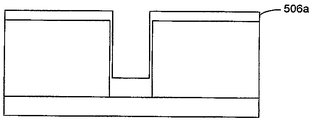
도 5A 내지 도 5F는 다수 사이클 증착-에치 옥사이드 층 형성 과정의 구체예를 사용함으로써 다층 실리콘 옥사이드 필름으로 단계적으로 충전되는 갭 구조물을 지니는 기판을 나타내고 있다. 도 5A는 갭(504)이 그 위에 형성되는 기판(502)을 나타내고 있다. 도 5A 내지 도 5F에 나타낸 갭(504)이 상대적으로 낮은 종횡비로 작도되어 옥사이드 충전 층의 성장을 더욱 명확히 나타내고 있음을 인지할 수 있을 것이다. 본 갭충전 방법의 구체예는 5:1, 6:1, 7:1, 8:1, 9:1, 10:1, 11:1, 12:1, 13:1, 14:1, 및 15:1 또는 그 초과의 종횡비를 지니는 갭으로의 공극 및 시임 없는 증착을 포함할 수 있다.
도 5B는 갭(504) 내에 증착된 제 1 옥사이드 층(506a)을 나타내고 있다. 층을 형성한 실리콘 옥사이드는 양호한 유동성 품질을 지녀서 필름이 갭(504)의 바닥으로 신속히 이동하게 한다. 따라서, 갭(504)의 바닥에 증착된 옥사이드의 두께는 갭의 측벽을 따른(along) 옥사이드 두께 보다 클 수 있다.
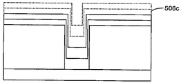
도 5C 및 도 5D는 갭(504) 내에 앞서 증착되고 에칭된 층상에 증착되는 추가의 옥사이드 층(506b, 506c 등)을 나타내고 있다. 이들 추가의 층은, 요구되는 옥사이드 필름 두께 수준이 도달될 때까지(예컨대, 갭(504)의 상부), 갭(504)내에서 바닥으로부터 상향으로 형성될 수 있다.
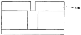
다수의 옥사이드 층 중의 마지막 층이 증착되고 에칭되면, 도 5E에 도시된 바와 같이, 어닐링이 수행되어 층을 균일한 필름(508)으로 형성시킬 수 있다. 필름은, 예를 들어, 플라즈마 에칭 또는 CMP에 의해서 평탄화되어서 갭(504)의 상부 상에 형성된 증착 재료를 제거할 수 있다. 도 5F는 만약에 있다면, 근소한 공극 또는 시임을 지니며 높은 필름-품질 및 유전 특성을 지니는 나머지 실리콘 옥사이드 갭충전(510)을 나타낸다.
예시적인 기판 가공 시스템
본 발명의 구체예를 실행할 수 있는 증착 시스템은, 다른 시스템 유형들 중에서도, 고밀도 플라즈마 화학적 기상 증착(high-density plasma chemical vapor deposition (HDP-CVD)) 시스템, 플라즈마 향상된 화학적 기상 증착(plasma enhanced chemical vapor deposition (PECVD)) 시스템, 감압하 화학적 기상 증착(sub-atmospheric chemical vapor deposition (SACVD)) 시스템, 및 열화학적 기상 증착 시스템을 포함할 수 있다. 본 발명의 구체예를 실행할 수 있는 CVD 시스템의 특정의 예는 미국 캘리포니아 산타 클라라 소재의 어플라이드 머티리얼스, 인코포레이티드로부터 구매할 수 있는 CENTURA ULTIMA™ HDP-CVD 챔버/시스템 및 PRODUCER™ PECVD 챔버/시스템을 포함한다.
본 발명의 예시적인 방법과 함께 사용될 수 있는 기판 가공 시스템의 예는 발명의 명칭이 "유전 갭충전을 위한 공정 챔버(PROCESS CHAMBER FOR DIELECTRIC GAPFILL)"인 2006년 5월 30일자 출원된 루보미르스키 등에 공동 양도된 미국가특허출원 제60/803,499에 도시되고 설명된 것들을 포함할 수 있으며, 본원에서는 모든 목적을 위하여 상기 특허출원의 전체 내용이 참조로 통합된다. 추가의 예시적인 시스템은 미국특허 제6,387,207호 및 제6,830,624호에 도시되고 설명된 것들을 포함할 수 있으며, 본원에서는 모든 목적을 위하여 상기 특허가 또한 참조로 통합된다.
이제 도 6A를 참조하면, 챔버벽(15a) 및 챔버 리드 어셈블리(chamber lid assembly: 15b)를 포함하는 진공 또는 가공 챔버(15)를 지닌 CVD 시스템(10)의 수직 단면도가 나타나 있다. CVD 시스템(10)은 가공 챔버(15) 내 중심에 있는 가열된 페데스탈(pedestal: 12) 상에 놓여 있는 기판(도시되지 않음)에 공정 가스를 분산시키는 가스 분배 매니폴드(11)를 함유한다. 가스 분배 매니폴드(11)는 용량 플라즈마(capacitive plasma)를 형성시키는 전극으로서 작용하게 하기 위해서 전기 전도성 재료로부터 형성될 수 있다. 가공 동안, 기판(예컨대, 반도체 웨이퍼)은 페데스탈(12)의 평탄(또는 약간 볼록) 표면(12a) 상에 정위된다. 페데스탈(12)은 매니폴드(11)에 아주 인접되는 상부 공정 위치(도 6A에서 점선(14)으로 표시됨)와 하부 로딩/오프-로딩 위치(도 6A에 도시됨) 사이를 조절가능하게 움직일 수 있다. 센터보드(도시되지 않음)는 웨이퍼의 위치에 대한 정보를 제공하는 센서를 포함한다.
증착 및 캐리어 가스는 통상의 평탄한 환형 가스 분배 페이스플레이트(faceplate: 13a)의 천공 홀(13b)을 통해서 챔버(15) 내로 도입된다. 더욱 특히, 증착 공정 가스는 유입 매니폴드(11)를 통해서, 통상의 천공된 블록커 플레이트(blocker plate)를 통해서, 및 이어서 가스 분배 페이스플레이트(13a) 내의 홀(hole: 13b)을 통해서 챔버 내로 흐른다.
매니폴드(11)에 도달하기 전에, 증착 및 캐리어 가스는 가스 공급 라인을 통해서 가스 공급원으로부터 혼합 시스템으로 유입되며, 그러한 혼합 시스템에서, 이들은 혼합되고 매니폴드(11)에 이송된다. 일반적으로, 각각의 공정 가스를 위한 공급 라인은 (i) 챔버 내로의 공정 가스의 흐름을 자동적으로 또는 수동적으로 차단하는데 이용될 수 있는 수 개의 안전 차단 밸브(도시되지 않음) 및 (ii) 공급 라인을 통한 가스 흐름을 측정하는 매스 플로우 제어기(mass flow controller)(또한 도시되지 않음)를 포함한다. 독성 가스가 공정에서 사용되는 경우, 수 개의 안전 차단 밸브가 통상의 형태로 각각의 가스 공급 라인상에 정위된다.
CVD 시스템(10)에서 수행되는 증착 공정은 열적 공정 또는 플라즈마-향상된 공정 중 하나 일 수 있다. 플라즈마-향상된 공정에서, RF 전력 공급기(RF power supply)는 공정 가스 혼합물을 여기시켜 페이스플레이트(13a)와 페데스탈(12) 사이의 실린더형 영역 내에 플라즈마를 형성시킬 수 있도록 전력을 가스 분배 페이스플레이트(13a)와 페데스탈(12) 사이에 가한다. (이러한 영역은 본원에서 "반응 영역"이라 칭한다). 플라즈마의 구성물은 반응하여 요구된 필름을 페데스탈(12) 상에 지지된 반도체 웨이퍼의 표면 상에 증착시킨다. RF 전력 공급기는 전형적으로 13.56MHz의 높은 RF 주파수(RF1) 및 360KHz의 낮은 RF 주파수(RF2)에서 전력을 공급하여 진공 챔버(15) 내로 도입된 반응성 화학종의 분해를 향상시키는 혼합된 주파수 RF 전력 공급기이다. 열적 공정에서는, RF 전력 공급기가 이용되지 않을 것이며, 공정 가스 혼합물이 열적으로 반응하여 반응을 위한 열에너지를 제공하도록 저항적으로 가열되는 페데스탈(12) 상에 지지된 반도체 웨이퍼의 표면 상에 요구되는 필름을 증착시킨다.
플라즈마-향상된 증착 공정 동안에, 플라즈마는 배출 통로(23)와 차단 밸브(24)를 둘러싸고 있는 챔버 보디(15a)의 벽을 포함한 전체 공정 챔버(10)를 가열한다. 플라즈마가 작동하지 않는 경우 또는 열 증착 공정 동안, 고온의 액체가 공정 챔버(15)의 벽(15a)을 통해서 순환하여 챔버를 상승된 온도로 유지시킨다. 챔버 벽(15a)의 나머지 부분에서의 통로는 도시되어 있지 않다. 챔버 벽(15a)을 가열하는데 사용되는 유체는 전형적인 유체 형태, 즉, 물-기재 에틸렌 글리콜 또는 오일-기재 열 전달 유체를 포함한다. 이러한 가열("열교환"에 의한 가열이라 칭함)은 바람직하지 않은 반응 생성물의 응축을 유리하게 감소 또는 제거하고, 냉각 진공 통로의 벽 상에서 응축되는 경우와 가스 흐름이 없는 시기동안 공정 챔버 내로 역으로 이동하는 경우에 공정을 오염시킬 수 있는 휘발성 공정 가스 생성물 및 그 밖의 오염물의 제거를 개선시킨다.
반응 부산물을 포함하여 층에 증착되지 않는 가스 혼합물의 나머지는 진공 펌프(도시되지 않음)에 의해서 챔버(15)로부터 배출된다. 특히, 가스는 반응 영역을 둘러싸고 있는 환형의 슬롯-모양 오리피스(16)를 통해서 및 환형의 배출 플레넘(17) 내로 배출된다. 환형의 슬롯(16) 및 플레넘(17)은 챔버의 실린더형 측벽(15a)(벽 상의 상부 유전체 라이닝(19)을 포함함)의 상부와 원형의 챔버 리드(20)의 바닥 사이의 갭에 의해서 규정된다. 슬롯 오리피스(16)와 플레넘(17)의 360° 원형 대칭 및 균일성은 웨이퍼 상에 균일한 필름을 증착시키기 위해서 웨이퍼 위에 공정 가스의 균일한 흐름을 달성하는데 중요하다.
배출 플레넘(17)으로부터, 가스는 배출 플레넘(17)의 측면 연장부(21) 밑으로 흘러서, 관찰 포트(viewing port)(도시되지 않음)를 통과하고, 하향-연장 가스 통로(23)를 통해서, 진공 차단 밸브(24)(이의 몸체는 하부 챔버 벽(15a)과 일체화됨)를 통과하고, 포어라인(foreline)(또한 도시되지 않음)을 통해서 외부 진공 펌프(도시되지 않음)에 연결되는 배출 출구(25) 내로 흐른다.
페데스탈(12)의 웨이퍼 지지 플레터(platter)(바람직하게는, 알루미늄, 세라믹, 또는 이의 조합물)는 평행 동심원의 형태로 두 개의 풀 턴(full turn)을 이루도록 구성된 내장형 단일-루프 내장 히터 엘리먼트를 사용함으로써 저항적으로 가열된다. 히터 엘리먼트의 외측의 부분은 지지 플레터의 주변에 인접하여 연장되어 있지만, 내측의 부분은 덕 작은 반경을 지니는 동심원의 경로 위에 연장되어 있다. 히터 엘리먼트에 대한 배선은 페데스탈(12)의 스템(stem)을 통해서 통과한다.
전형적으로는, 챔버 라이닝, 가스 유입 매니폴드 페이스플레이트, 및 다양한 그 밖의 반응기 하드웨어의 전부 또는 임의의 하나는 알루미늄, 아노다이징 처리된(anodized) 알루미늄, 또는 세라믹과 같은 재료로 제조된다. 그러한 CVD 장치의 예는 쟈오(Zhao) 등에게 허여된 발명의 명칭 "CVD 공정 챔버(CVD Processing Chamber)"의 공동 양도된 미국특허 제5,558,717호에 기재되어 있으며, 본원에서는 상기 특허의 모든 내용이 참조로 통합된다.
리프트 메카니즘 및 모터(32)(도 6A)는, 웨이퍼가 챔버(10)의 측면내의 삽입/제거 구멍(26)을 통해서 로봇 블레이드(blade)(도시되지 않음)에 의해서 챔버(15)의 몸체 내로 및 그 외부로 전달되도록, 히터 페데스탈 어셈블리(12) 및 이의 웨이퍼 리프트 핀(12b)을 상승 및 하강시킨다. 모터(32)는 공정 위치(14)와 하부 웨이퍼-로딩 위치 사이로 페데스탈(12)을 상승 및 하강시킨다. 모터, 공급 라인에 연결된 밸브 또는 흐름 제어기, 가스 전달 시스템, 트로틀 밸브, RF 전력 공급기, 및 챔버 및 기판 가열 시스템은 모두 제어 라인을 통하여 시스템 제어기에 의해서 제어되며, 이들 중 단지 일부만이 도시되어 있다. 제어기는 광학 센서로부터의 피드백에 따라서 제어기의 제어하의 적절한 모터에 의해서 움직이는 트로틀 밸브 및 서셉터(susceptor)와 같은 운동가능한 기계적 어셈블리의 위치를 결정한다.
예시적인 구체예에서, 시스템 제어기는 하드 디스크 드라이브(메모리), 플로피 디스크 드라이브 및 프로세서를 포함한다. 프로세서는 싱글-보드 컴퓨터(single-board computer (SBC)), 아날로그 및 디지탈 인풋/아웃풋 보드, 인터 페이스 보드 및 스테퍼 모터 제어 보드(stepper motor controller board)를 함유한다. CVD 시스템(10)의 다양한 부분은 보드, 카드 케이지, 및 커넥터 치수 및 형태를 규정하는 베르사 모듈러 유러피언(Versa Modular European (VME)) 표준에 부합한다. VME 표준은 또한 16-비트 데이타 버스(data bus) 및 24-비트 어드레스 버스(address bus)를 지니는 버스 구조(bus structure)를 규정하고 있다.
시스템 제어기는 CVD 기계의 모든 활성을 제어한다. 시스템 제어기는 시스템 제어 소프트웨어를 실행하며, 그러한 소프트웨어는 컴퓨터-판독가능한 매체, 예컨대, 메모리에 저장된 컴퓨터 프로그램이다. 바람직하게는, 메모리는 하드 디스크 드라이브이지만, 메모리는 또한 그 밖의 종류의 메모리일 수 있다. 컴퓨터 프로그램은 타이밍, 가스 혼합, 챔버 압력, 챔버 온도, RF 전력 수준, 서셉터 위치, 및 그 밖의 특정 공정의 파라메터를 지시하는 지침서 세트를 포함한다. 예를 들어, 플로피 디스크 또는 그 밖의 다른 적절한 드라이브를 포함한 다른 메모리 장치에 저장된 그 밖의 컴퓨터 프로그램이 또한 제어기를 작동시키는데 이용될 수 있다.
기판 상에 필름을 증착시키는 공정 또는 챔버(15)를 세정하는 공정은 제어기에 의해서 실행되는 컴퓨터 프로그램 제품을 사용함으로써 실행될 수 있다. 컴퓨터 프로그램 코드는 어떠한 통상의 컴퓨터 판독 가능한 프로그래밍 언어, 예를 들어, 68000 어셈블리 언어, C, C++, 파스칼, 포트란 또는 그 밖의 언어로 작성될 수 있다. 적합한 프로그램 코드는 통상의 텍스트 편집기를 사용함으로써 싱글 파일, 또는 멀티플 파일에 입력되고, 컴퓨터 이용가능한 매체, 예컨대, 컴퓨터의 메모리 시스템에 저장 또는 내장된다. 입력된 코드 텍스트가 고급 언어로 된 경우, 코드가 컴파일링되고, 생성되는 컴파일러 코드가 이어서 미리 컴파일링된 Microsoft Windows® 라이브러리 루틴의 대상 코드와 링크된다. 링크되고 컴파일링된 대상 코드를 실행시키기 위해서, 시스템 사용자는 대상 코드를 불러내서 컴퓨터 시스템이 코드를 메모리에 로딩하게 한다. CPU는 이어서 코드를 판독하고 실행하여 프로그램에서 확인된 작업을 수행한다.
사용자와 제어기 사이의 인터페이스는 하나 이상의 챔버를 포함할 수 있는 기판 가공 시스템 중의 시스템 모니터 및 CVD 시스템(10)의 단순 개략도인 도 6B에 도시된 바와 같은 CRT 모니터(50a) 및 라이트 펜(light pen: 50b)을 통해서 행해진다. 바람직한 구체예에서, 두 모니터(50a)가 사용되는데, 하나는 작업자를 위해서 클린 룸 벽(clean room wall)에 장착되고 다른 하나는 서비스 기술자를 위해서 벽의 뒤에 장착된다. 모니터(50a)는 동일한 정보를 동시에 디스플레이하지만, 단지 하나의 라이트 펜(50b)만 사용할 수 있다. 라이트 펜(50b)의 팁에서의 광 센서는 CRT 디스플레이에 의해서 방출된 광을 검출한다. 특정의 스크린 또는 기능을 선택하기 위해서, 작업자는 디스플레이 스크린의 지정된 부위를 터치하고 펜(50b) 상의 버튼을 누른다. 터치된 부위는 그의 하이라이트된 색을 변화시키거나, 새로운 메뉴 또는 스크린이 디스플레이되어, 라이트 펜과 디스플레이 스크린 사이의 통신을 확인한다. 그 밖의 디바이스, 예컨대, 키보드, 마우스, 또는 다른 포인팅 또는 통신 장치가 라이트 펜(50b) 대신 또는 그에 추가로 사용되어 사용자가 제어기와 통신할 수 있게 할 수 있다.
도 6A는 가스 분배 페이스플레이트(13a)와 가스 분배 매니폴드(11)를 포함하는 공정 챔버(15)의 리드 어셈블리(lid assembly: 15b) 상에 장착된 원격 플라즈마 생성장치(60)를 나타낸다. 장착 어뎁터(adaptor: 64)는 도 6A에 가장 잘 도시된 바와 같이 리드 어셈블리(15b) 상에 원격 플라즈마 생성장치(60)를 장착시킨다. 어뎁터(64)는 전형적으로는 금속으로 제조된다. 혼합 장치(70)가 가스 분배 매니폴드(11)의 상류 측에 결합되어 있다(도 6A). 혼합 장치(70)는 공정 가스를 혼합하는 혼합 블록의 슬롯 내부에 위치한 혼합 인서트(mixing insert: 72)를 포함한다. 세라믹 절연체(66)가 장착 어뎁터(64)와 혼합 장치(70) 사이에 위치한다(도 6A). 세라믹 절연체(66)는 세라믹 재료, 예컨대, Al2O3(99% 순도), 테플론®(Teflon®) 등으로 제조될 수 있다. 설치되었을 때, 혼합 장치(70)와 세라믹 절연체(66)는 리드 어셈블리(15b)의 일부를 형성할 수 있다. 절연체(66)는 혼합 장치(70)와 가스 분배 매니폴드(11)로부터 금속 어뎁터(64)를 분리시켜서 이차 플라즈마의 잠재성을 최소로 하여 이하 더 상세히 논의되는 바와 같은 리드 어셈블리(15b)를 형성시킨다. 3-웨이 밸브(77)는 직접적으로 또는 원격 플라즈마 생성장치(60)를 통하여 공정 챔버(15)로의 공정 가스의 흐름을 제어한다.
원격 플라즈마 생성장치(60)는 바람직하게는 리드 어셈블리(15b) 상에 통상적으로 장착될 수 있는 콤팩트한 내장형 유닛(self-contained unit)이며 비용 및 시간 소모적인 변화 없이 기존의 챔버에 용이하게 개조된다. 한 가지 적합한 유닛은 미국 매사추세츠 우번 소재의 어플라이드 사이언스 앤드 테크놀로지, 인코포레이티드(Applied Science and Technology, Inc.)로부터 구매할 수 있는 ASTRON® 생성장치이다. ASTRON® 생성장치는 낮은-장 토로이달 플라즈마(low-field toroidal plasma)를 이용하여 공정 가스를 해리시킨다. 한 가지 예에서, 플라즈마는 NF3와 같은 불소-함유 가스, 및 아르곤과 같은 캐리어 가스를 포함한 공정 가스를 해리시켜서 공정 챔버(15) 중의 필름 증착물을 세정하는데 사용되는 유리 불소를 생성시킨다.
상기된 몇가지 구체예를 보면, 당업자라면 본 발명의 사상을 벗어나지 않으면서 다양한 변화, 대안적인 구성 및 등가물이 이용될 수 있다는 것을 인지할 수 있을 것이다. 추가로, 본 발명을 불필요하게 불명료하게 하는 것을 피하기 위해서, 많은 잘 공지된 공정 및 엘리먼트가 기재되지 않는다. 따라서, 상기 설명은 본 발명의 범위를 한정하는 것으로 취급되지 않아야 한다.
일정 범위의 값이 제공되는 경우, 그 문맥이 명확히 달리 명시하지 않는 한, 하한 값의 단위의 10분지 1까지에 이르는, 그 범위의 상한과 하한 사이의 각각의 중간값이 또한 특별히 개시되는 것으로 이해될 것이다. 어떠한 언급된 값 또는 언급된 범위 중의 중간값과 그 언급된 범위 내의 어떠한 다른 언급된 값 또는 중간값 사이의 각각의 더 작은 범위가 포함된다. 이들 더 작은 범위의 상한 및 하한은 독립적으로 범위 내에 포함되거나 배제될 수 있으며, 그 상한과 하한 둘 중 하나 또는 둘 다가 더 작은 범위에 포함되거나 둘 중 어느 것도 더 작은 범위에 포함되지 않는 각각의 범위가 또한, 언급된 범위 내의 어떠한 특정적으로 배제된 한계를 조건으로, 본 발명의 범위 내에 포함된다. 언급된 범위가 한계 중 하나 또는 둘 모두를 포함하는 경우, 이들 포함된 한계 중 둘 모두 또는 둘 중 하나를 배제하는 범위가 또한 포함된다.
본원 및 첨부된 청구범위에서 사용된 표현인 단수형은, 문장이 명확히 달리 명시하지 않는 한, 복수의 대상물을 포함한다. 따라서, 예를 들어 "방법"에 관해 언급하는 것은 다수의 그러한 방법의 복수를 포함하며, "전구체"에 관해 언급하는 것은 하나 이상의 전구체 및 본 기술 분야의 전문가에게는 공지된 그 등가물에 관해서 언급하는 것을 포함한다.
또한, 본 명세서 및 하기 청구범위에서 사용되는 용어 "포함한다", "포함한", "포함하는"은 언급된 특징물, 수치, 성분 또는 단계의 존재를 명시하는 것으로 의도되지만, 이들은 하나 이상의 다른 특징물, 수치, 성분, 단계, 작용, 또는 그룹의 존재 또는 부가를 배제하는 것이 아니다.
본 발명의 특징 및 이점에 대한 추가의 이해는 명세서의 남은 부분 및 유사한 참조 번호가 몇 개의 도면 전체에서 유사한 성분을 나타내고 있는 도면을 참조하여 실현될 수 있다. 일부 예에서, 서브라벨은 참조 번호와 관련이 있으며, 하이픈 다음에 와서 다수의 유사한 성분 중 하나를 의미한다. 참조가 기존의 서브라벨에 대한 명시 없이 참조 번호로 기재되는 경우, 모든 그러한 다수의 유사한 성분을 나타내고자 하는 것으로 의도된다.
도 1은 본 발명의 구체예에 따른 유전 증착의 단순 개요를 나타내는 플로우챠트이다.
도 2는 본 발명의 구체예에 따른 갭을 유전 재료로 충전시키는 방법을 예시하는 플로우챠트이다.
도 3은 본 발명의 구체예에 따른 기판 상의 갭 내에 유전 재료를 증착시키고 어닐링하는 단계를 나타내는 플로우챠트이다.
도 4는 본 발명의 구체예에 따른 다층 실리콘 옥사이드 필름을 제조하는 방법을 예시하는 플로우챠트이다.
도 5A 내지 도 5F는 본 발명의 구체예에 따른 다층 실리콘 옥사이드 필름으로 단계적으로 충전된 갭 구조를 지니는 기판을 나타낸다.
도 6A는 본 발명의 구체예에 따른 실리콘 옥사이드 층을 형성시키는데 사용될 수 있는 기판 가공 시스템의 수직 단면도를 나타낸다.
도 6B는 본 발명의 구체예에 따른 기판 가공 시스템의 시스템 모니터/제어기 부품의 단순 설계도를 나타낸다.
Claims (37)
- 기판에 형성된 갭에 유전층을 증착시키는 방법으로서,
8 미만의 C:Si 원자비율을 지니는 유기-실리콘 전구체 및 증착 챔버의 외부에서 생성되는 원자 산소를 포함하는 산소 전구체를 증착 챔버에 도입하고,
전구체를 반응시켜 갭내에 유전층을 형성시킴을 포함하여, 기판에 형성된 갭에 유전층을 증착시키는 방법. - 제 1항에 있어서, 유기-실리콘 전구체가 3 초과의 O:Si 비율을 지니는 방법.
- 제 1항에 있어서, 유기-실리콘 전구체가 4 초과의 O:Si 비율을 지니는 방법.
- 제 1항에 있어서, 유기-실리콘 전구체가 Si-O-Si 결합을 포함하는 방법.
- 제 1항에 있어서, 유기-실리콘 전구체가 실록산을 포함하는 방법.
- 제 5항에 있어서, 실록산이 트리에톡시실록산, 테트라메톡시실록산, 트리메톡시실록산, 헥사메톡시디실록산, 옥타메톡시트리실록산, 및 옥타메톡시도데카실록산으로 이루어진 군으로부터 선택되는 방법.
- 제 1항에 있어서, 유기-실리콘 전구체가 실라족산을 포함하는 방법.
- 제 7항에 있어서, 실라족산이 헥사메톡시디실라족산, 메틸 헥사메톡시디실라족산, 클로로헥사메톡시디실라족산, 헥사에톡시디실라족산, 옥타메톡시시클릭실라족산, 및 노나메톡시트리실라족산으로 이루어진 군으로부터 선택되는 방법.
- 제 1항에 있어서, 유기-실리콘 전구체가 할로겐화된 실록산을 포함하는 방법.
- 제 9항에 있어서, 할로겐화된 실록산이 테트라클로로실란, 디클로로디에톡시실록산, 클로로트리에톡시실록산, 헥사클로로디실록산, 및 옥타클로로트리실록산으로 이루어진 군으로부터 선택되는 방법.
- 제 1항에 있어서, 유기-실리콘 전구체가 아미노실란, 알킬 디실란, 알콕시 디실란, 알콕시-알킬 디실란, 알콕시-아세톡시 디실란, 또는 시클로실란을 포함하는 방법.
- 제 1항에 있어서, 산소 전구체가 분자 산소, 오존, 물, 과산화수소, 또는 이산화질소를 추가로 포함하는 방법.
- 제 1항에 있어서, 원자 산소가 아르곤을 포함하는 가스 혼합물로부터 플라즈마를 형성시키고; 해리되어 원자 산소를 형성하는 산소 공급원을 플라즈마에 도입함에 의해서 형성되는 방법.
- 제 13항에 있어서, 산소 공급원이 분자 산소, 오존 또는 이산화질소를 포함하는 방법.
- 제 1항에 있어서, 유기-실리콘 및 산소 전구체로부터 증착챔버에 플라즈마를 형성시킴을 추가로 포함하는 방법.
- 제 1항에 있어서, 유전층을 에칭하여 층중의 탄소 함량을 감소시킴을 추가로 포함하는 방법.
- 제 1항에 있어서, 갭내의 유전층을 어닐링함을 추가로 포함하는 방법.
- 갭을 유전재료로 충전하는 방법으로서,
8 미만의 C:Si 원자 비율을 지니는 유기-실리콘 전구체 및 산소 전구체를 증착 챔버에 제공하고;
갭에 유전 재료의 제 1 부분을 증착시키는 플라즈마를 증착 챔버에서 전구체로부터 생성시키고;
유전 재료의 제 1 부분을 에칭시켜서 재료중의 탄소 함량을 감소시키고;
갭에 유전 재료의 제 2 부분을 증착시키고;
갭내의 유전 재료의 제 1 부분 및 제 2 부분을 어닐링함을 포함하여, 갭을 유전재료로 충전하는 방법. - 제 18항에 있어서, 유기-실리콘 전구체가 약 6 또는 그 미만의 C:Si 비율을 지니는 방법.
- 제 18항에 있어서, 유기-실리콘 전구체가 약 3 또는 그 초과의 O:Si 비율을 지니는 방법.
- 제 18항에 있어서, 유기-실리콘 전구체가 Si-O-Si 결합을 포함하는 방법.
- 제 18항에 있어서, 유기-실리콘 전구체가 실라족산을 포함하는 방법.
- 제 22항에 있어서, 실리족산내의 Si-N 결합을 산화시키고 Si-O 결합을 형성시킴을 포함하는 방법.
- 제 23항에 있어서, Si-N 결합이 원격 생성된 원자 산소 전구체에 의해서 산화되는 방법.
- 제 18항에 있어서, 유기-실리콘 전구체가 할로겐화된 실록산을 포함하는 방법.
- 제 25항에 있어서, 할로겐화된 실록산중의 Si-X 결합을 산화시키고 Si-O 결합을 형성시킴을 포함하며, 상기 X가 할로겐 원자인 방법.
- 제 18항에 있어서, 어닐링 전에 유전 재료의 제 2 부분을 에칭시킴을 포함하는 방법.
- 제 18항에 있어서, 산소 전구체가 증착 챔버 외부에서 생성되는 원자 산소를 포함하는 방법.
- 기판상의 갭에 유전 재료를 증착시키고 어닐링하는 방법으로서,
8 미만의 C:Si 원자 비율을 지니는 유기-실리콘 전구체 및 산소 전구체를 증착 챔버에 제공하고;
전구체를 반응시켜서 갭에 유전 재료를 증착시키고;
증착된 유전 재료에 대한 열적 어닐링을 수행하고;
증착된 유전 재료에 대한 플라즈마 어닐링을 수행함을 포함하여, 기판상의 갭에 유전 재료를 증착시키고 어닐링하는 방법. - 제 29항에 있어서, 열적 어닐링이 유전 재료를 약 300℃ 내지 약 600℃의 온도로 약 1 분 내지 약 30분 동안 가열함을 포함하는 방법.
- 제 29항에 있어서, 플라즈마 어닐링이 유전 재료를 고밀도 플라즈마에 약 1 분 내지 약 10분 동안 노출시킴을 포함하는 방법.
- 제 29항에 있어서, 유기-실리콘 전구체가 약 6 또는 그 미만의 C:Si 비율을 지니는 방법.
- 제 29항에 있어서, 유기-실리콘 전구체가 약 3 또는 그 초과의 O:Si 비율을 지니는 방법.
- 제 29항에 있어서, 유기-실리콘 전구체가 Si-O-Si 결합을 포함하는 방법.
- 제 29항에 있어서, 유기-실리콘 전구체가 실록산을 포함하는 방법.
- 제 29항에 있어서, 유기-실리콘 전구체가 실라족산 또는 할로겐화된 실록산을 포함하는 방법.
- 제 29항에 있어서, 산소 전구체가 증착 챔버 외부에서 생성되는 원자 산소를 포함하는 방법.
Applications Claiming Priority (3)
| Application Number | Priority Date | Filing Date | Title |
|---|---|---|---|
| US11/549,930 | 2006-10-16 | ||
| US11/549,930 US7498273B2 (en) | 2006-05-30 | 2006-10-16 | Formation of high quality dielectric films of silicon dioxide for STI: usage of different siloxane-based precursors for harp II—remote plasma enhanced deposition processes |
| PCT/US2007/081139 WO2008048862A2 (en) | 2006-10-16 | 2007-10-11 | Formation of high quality dielectric films of silicon dioxide for sti: usage of different siloxane-based precursors for harp ii - remote plasma enhanced deposition processes |
Related Parent Applications (1)
| Application Number | Title | Priority Date | Filing Date |
|---|---|---|---|
| KR1020097010045A Division KR101329285B1 (ko) | 2006-10-16 | 2007-10-11 | 에스티아이를 위한 실리콘 디옥사이드의 고품질 유전 필름의 제조: 하프 ⅱ― 원격 플라즈마 향상된 증착 공정을 위한 상이한 실록산―기재 전구체의 용도 |
Publications (1)
| Publication Number | Publication Date |
|---|---|
| KR20130114269A true KR20130114269A (ko) | 2013-10-16 |
Family
ID=38983940
Family Applications (2)
| Application Number | Title | Priority Date | Filing Date |
|---|---|---|---|
| KR1020137023298A KR20130114269A (ko) | 2006-10-16 | 2007-10-11 | 에스티아이를 위한 실리콘 디옥사이드의 고품질 유전 필름의 제조: 하프 ⅱ― 원격 플라즈마 향상된 증착 공정을 위한 상이한 실록산―기재 전구체의 용도 |
| KR1020097010045A KR101329285B1 (ko) | 2006-10-16 | 2007-10-11 | 에스티아이를 위한 실리콘 디옥사이드의 고품질 유전 필름의 제조: 하프 ⅱ― 원격 플라즈마 향상된 증착 공정을 위한 상이한 실록산―기재 전구체의 용도 |
Family Applications After (1)
| Application Number | Title | Priority Date | Filing Date |
|---|---|---|---|
| KR1020097010045A KR101329285B1 (ko) | 2006-10-16 | 2007-10-11 | 에스티아이를 위한 실리콘 디옥사이드의 고품질 유전 필름의 제조: 하프 ⅱ― 원격 플라즈마 향상된 증착 공정을 위한 상이한 실록산―기재 전구체의 용도 |
Country Status (7)
| Country | Link |
|---|---|
| US (1) | US7498273B2 (ko) |
| EP (2) | EP2503022A1 (ko) |
| JP (2) | JP4987083B2 (ko) |
| KR (2) | KR20130114269A (ko) |
| CN (1) | CN101528974B (ko) |
| TW (1) | TWI349309B (ko) |
| WO (1) | WO2008048862A2 (ko) |
Families Citing this family (142)
| Publication number | Priority date | Publication date | Assignee | Title |
|---|---|---|---|---|
| US7524735B1 (en) | 2004-03-25 | 2009-04-28 | Novellus Systems, Inc | Flowable film dielectric gap fill process |
| US9257302B1 (en) * | 2004-03-25 | 2016-02-09 | Novellus Systems, Inc. | CVD flowable gap fill |
| US7582555B1 (en) | 2005-12-29 | 2009-09-01 | Novellus Systems, Inc. | CVD flowable gap fill |
| JP2006261434A (ja) | 2005-03-17 | 2006-09-28 | L'air Liquide Sa Pour L'etude & L'exploitation Des Procede S Georges Claude | シリコン酸化膜の形成方法 |
| US7790634B2 (en) * | 2006-05-30 | 2010-09-07 | Applied Materials, Inc | Method for depositing and curing low-k films for gapfill and conformal film applications |
| US7825038B2 (en) * | 2006-05-30 | 2010-11-02 | Applied Materials, Inc. | Chemical vapor deposition of high quality flow-like silicon dioxide using a silicon containing precursor and atomic oxygen |
| US20070277734A1 (en) * | 2006-05-30 | 2007-12-06 | Applied Materials, Inc. | Process chamber for dielectric gapfill |
| US7902080B2 (en) * | 2006-05-30 | 2011-03-08 | Applied Materials, Inc. | Deposition-plasma cure cycle process to enhance film quality of silicon dioxide |
| US8232176B2 (en) * | 2006-06-22 | 2012-07-31 | Applied Materials, Inc. | Dielectric deposition and etch back processes for bottom up gapfill |
| US7888273B1 (en) * | 2006-11-01 | 2011-02-15 | Novellus Systems, Inc. | Density gradient-free gap fill |
| US9245739B2 (en) | 2006-11-01 | 2016-01-26 | Lam Research Corporation | Low-K oxide deposition by hydrolysis and condensation |
| JP5024527B2 (ja) * | 2007-03-27 | 2012-09-12 | Jsr株式会社 | 膜形成方法、及びトレンチアイソレーションの形成方法 |
| US7745352B2 (en) * | 2007-08-27 | 2010-06-29 | Applied Materials, Inc. | Curing methods for silicon dioxide thin films deposited from alkoxysilane precursor with harp II process |
| EP2193541A1 (en) * | 2007-09-18 | 2010-06-09 | L'AIR LIQUIDE, Société Anonyme pour l'Etude et l'Exploitation des Procédés Georges Claude | Method of forming silicon-containing films |
| US7943531B2 (en) * | 2007-10-22 | 2011-05-17 | Applied Materials, Inc. | Methods for forming a silicon oxide layer over a substrate |
| US7867923B2 (en) * | 2007-10-22 | 2011-01-11 | Applied Materials, Inc. | High quality silicon oxide films by remote plasma CVD from disilane precursors |
| US7803722B2 (en) | 2007-10-22 | 2010-09-28 | Applied Materials, Inc | Methods for forming a dielectric layer within trenches |
| US8357435B2 (en) * | 2008-05-09 | 2013-01-22 | Applied Materials, Inc. | Flowable dielectric equipment and processes |
| US20100081293A1 (en) * | 2008-10-01 | 2010-04-01 | Applied Materials, Inc. | Methods for forming silicon nitride based film or silicon carbon based film |
| US8557712B1 (en) * | 2008-12-15 | 2013-10-15 | Novellus Systems, Inc. | PECVD flowable dielectric gap fill |
| US8980382B2 (en) * | 2009-12-02 | 2015-03-17 | Applied Materials, Inc. | Oxygen-doping for non-carbon radical-component CVD films |
| US8741788B2 (en) * | 2009-08-06 | 2014-06-03 | Applied Materials, Inc. | Formation of silicon oxide using non-carbon flowable CVD processes |
| US7935643B2 (en) * | 2009-08-06 | 2011-05-03 | Applied Materials, Inc. | Stress management for tensile films |
| US7989365B2 (en) * | 2009-08-18 | 2011-08-02 | Applied Materials, Inc. | Remote plasma source seasoning |
| KR101114582B1 (ko) | 2009-08-31 | 2012-02-27 | 기아자동차주식회사 | 암레스트 일체형 리어 모니터 장착구조 |
| US8222145B2 (en) * | 2009-09-24 | 2012-07-17 | Dupont Air Products Nanomaterials, Llc | Method and composition for chemical mechanical planarization of a metal-containing substrate |
| US8278224B1 (en) | 2009-09-24 | 2012-10-02 | Novellus Systems, Inc. | Flowable oxide deposition using rapid delivery of process gases |
| US20110136347A1 (en) * | 2009-10-21 | 2011-06-09 | Applied Materials, Inc. | Point-of-use silylamine generation |
| US8449942B2 (en) * | 2009-11-12 | 2013-05-28 | Applied Materials, Inc. | Methods of curing non-carbon flowable CVD films |
| TWI579916B (zh) | 2009-12-09 | 2017-04-21 | 諾菲勒斯系統公司 | 整合可流動氧化物及頂蓋氧化物之新穎間隙填充 |
| US20110151677A1 (en) * | 2009-12-21 | 2011-06-23 | Applied Materials, Inc. | Wet oxidation process performed on a dielectric material formed from a flowable cvd process |
| US8551887B2 (en) | 2009-12-22 | 2013-10-08 | Air Products And Chemicals, Inc. | Method for chemical mechanical planarization of a copper-containing substrate |
| JP2013516763A (ja) | 2009-12-30 | 2013-05-13 | アプライド マテリアルズ インコーポレイテッド | フレキシブルな窒素/水素比を使用して生成されるラジカルを用いる誘電体膜成長 |
| US8329262B2 (en) * | 2010-01-05 | 2012-12-11 | Applied Materials, Inc. | Dielectric film formation using inert gas excitation |
| SG182336A1 (en) | 2010-01-06 | 2012-08-30 | Applied Materials Inc | Flowable dielectric using oxide liner |
| CN102714156A (zh) | 2010-01-07 | 2012-10-03 | 应用材料公司 | 自由基成分cvd的原位臭氧固化 |
| US8703625B2 (en) | 2010-02-04 | 2014-04-22 | Air Products And Chemicals, Inc. | Methods to prepare silicon-containing films |
| US8361338B2 (en) | 2010-02-11 | 2013-01-29 | Taiwan Semiconductor Manufacturing Company, Ltd. | Hard mask removal method |
| KR101853802B1 (ko) * | 2010-03-05 | 2018-05-02 | 어플라이드 머티어리얼스, 인코포레이티드 | 라디칼성분 cvd에 의한 컨포멀 층들 |
| US8236708B2 (en) | 2010-03-09 | 2012-08-07 | Applied Materials, Inc. | Reduced pattern loading using bis(diethylamino)silane (C8H22N2Si) as silicon precursor |
| JP5563860B2 (ja) * | 2010-03-26 | 2014-07-30 | 東京エレクトロン株式会社 | 基板処理方法 |
| US7994019B1 (en) | 2010-04-01 | 2011-08-09 | Applied Materials, Inc. | Silicon-ozone CVD with reduced pattern loading using incubation period deposition |
| US8476142B2 (en) | 2010-04-12 | 2013-07-02 | Applied Materials, Inc. | Preferential dielectric gapfill |
| US20110256734A1 (en) | 2010-04-15 | 2011-10-20 | Hausmann Dennis M | Silicon nitride films and methods |
| US8637411B2 (en) | 2010-04-15 | 2014-01-28 | Novellus Systems, Inc. | Plasma activated conformal dielectric film deposition |
| US9611544B2 (en) | 2010-04-15 | 2017-04-04 | Novellus Systems, Inc. | Plasma activated conformal dielectric film deposition |
| US9390909B2 (en) | 2013-11-07 | 2016-07-12 | Novellus Systems, Inc. | Soft landing nanolaminates for advanced patterning |
| US9997357B2 (en) | 2010-04-15 | 2018-06-12 | Lam Research Corporation | Capped ALD films for doping fin-shaped channel regions of 3-D IC transistors |
| US9076646B2 (en) | 2010-04-15 | 2015-07-07 | Lam Research Corporation | Plasma enhanced atomic layer deposition with pulsed plasma exposure |
| US9373500B2 (en) | 2014-02-21 | 2016-06-21 | Lam Research Corporation | Plasma assisted atomic layer deposition titanium oxide for conformal encapsulation and gapfill applications |
| US9257274B2 (en) | 2010-04-15 | 2016-02-09 | Lam Research Corporation | Gapfill of variable aspect ratio features with a composite PEALD and PECVD method |
| US9892917B2 (en) | 2010-04-15 | 2018-02-13 | Lam Research Corporation | Plasma assisted atomic layer deposition of multi-layer films for patterning applications |
| US8956983B2 (en) | 2010-04-15 | 2015-02-17 | Novellus Systems, Inc. | Conformal doping via plasma activated atomic layer deposition and conformal film deposition |
| US8524004B2 (en) | 2010-06-16 | 2013-09-03 | Applied Materials, Inc. | Loadlock batch ozone cure |
| JP5490753B2 (ja) * | 2010-07-29 | 2014-05-14 | 東京エレクトロン株式会社 | トレンチの埋め込み方法および成膜システム |
| US8318584B2 (en) | 2010-07-30 | 2012-11-27 | Applied Materials, Inc. | Oxide-rich liner layer for flowable CVD gapfill |
| US9685320B2 (en) | 2010-09-23 | 2017-06-20 | Lam Research Corporation | Methods for depositing silicon oxide |
| US8524612B2 (en) | 2010-09-23 | 2013-09-03 | Novellus Systems, Inc. | Plasma-activated deposition of conformal films |
| US9285168B2 (en) | 2010-10-05 | 2016-03-15 | Applied Materials, Inc. | Module for ozone cure and post-cure moisture treatment |
| US8664127B2 (en) | 2010-10-15 | 2014-03-04 | Applied Materials, Inc. | Two silicon-containing precursors for gapfill enhancing dielectric liner |
| US8685867B1 (en) | 2010-12-09 | 2014-04-01 | Novellus Systems, Inc. | Premetal dielectric integration process |
| US9719169B2 (en) | 2010-12-20 | 2017-08-01 | Novellus Systems, Inc. | System and apparatus for flowable deposition in semiconductor fabrication |
| JP5675331B2 (ja) * | 2010-12-27 | 2015-02-25 | 東京エレクトロン株式会社 | トレンチの埋め込み方法 |
| US10283321B2 (en) | 2011-01-18 | 2019-05-07 | Applied Materials, Inc. | Semiconductor processing system and methods using capacitively coupled plasma |
| US8450191B2 (en) | 2011-01-24 | 2013-05-28 | Applied Materials, Inc. | Polysilicon films by HDP-CVD |
| US8716154B2 (en) | 2011-03-04 | 2014-05-06 | Applied Materials, Inc. | Reduced pattern loading using silicon oxide multi-layers |
| TW201245289A (en) * | 2011-03-11 | 2012-11-16 | Dow Corning | Polysilanesiloxane copolymers and method of converting to silicon dioxide |
| US8445078B2 (en) | 2011-04-20 | 2013-05-21 | Applied Materials, Inc. | Low temperature silicon oxide conversion |
| US8466073B2 (en) | 2011-06-03 | 2013-06-18 | Applied Materials, Inc. | Capping layer for reduced outgassing |
| US9404178B2 (en) | 2011-07-15 | 2016-08-02 | Applied Materials, Inc. | Surface treatment and deposition for reduced outgassing |
| KR101432606B1 (ko) * | 2011-07-15 | 2014-08-21 | 제일모직주식회사 | 갭필용 충전제, 이의 제조 방법 및 이를 사용한 반도체 캐패시터의 제조 방법 |
| WO2013043330A1 (en) * | 2011-09-23 | 2013-03-28 | Novellus Systems, Inc. | Plasma activated conformal dielectric film deposition |
| US8617989B2 (en) | 2011-09-26 | 2013-12-31 | Applied Materials, Inc. | Liner property improvement |
| US8993072B2 (en) | 2011-09-27 | 2015-03-31 | Air Products And Chemicals, Inc. | Halogenated organoaminosilane precursors and methods for depositing films comprising same |
| US8551891B2 (en) | 2011-10-04 | 2013-10-08 | Applied Materials, Inc. | Remote plasma burn-in |
| US8461016B2 (en) | 2011-10-07 | 2013-06-11 | Micron Technology, Inc. | Integrated circuit devices and methods of forming memory array and peripheral circuitry isolation |
| US9809711B2 (en) | 2012-01-17 | 2017-11-07 | Versum Materials Us, Llc | Catalyst and formulations comprising same for alkoxysilanes hydrolysis reaction in semiconductor process |
| US8592328B2 (en) | 2012-01-20 | 2013-11-26 | Novellus Systems, Inc. | Method for depositing a chlorine-free conformal sin film |
| JP5761724B2 (ja) * | 2012-01-24 | 2015-08-12 | 文彦 廣瀬 | 薄膜形成方法および装置 |
| US8728955B2 (en) | 2012-02-14 | 2014-05-20 | Novellus Systems, Inc. | Method of plasma activated deposition of a conformal film on a substrate surface |
| US8846536B2 (en) | 2012-03-05 | 2014-09-30 | Novellus Systems, Inc. | Flowable oxide film with tunable wet etch rate |
| US20130243968A1 (en) | 2012-03-16 | 2013-09-19 | Air Products And Chemicals, Inc. | Catalyst synthesis for organosilane sol-gel reactions |
| US9460912B2 (en) | 2012-04-12 | 2016-10-04 | Air Products And Chemicals, Inc. | High temperature atomic layer deposition of silicon oxide thin films |
| CN103515285B (zh) * | 2012-06-28 | 2018-03-27 | 联华电子股份有限公司 | 半导体结构及其制作工艺 |
| US8889566B2 (en) | 2012-09-11 | 2014-11-18 | Applied Materials, Inc. | Low cost flowable dielectric films |
| KR102207992B1 (ko) | 2012-10-23 | 2021-01-26 | 램 리써치 코포레이션 | 서브-포화된 원자층 증착 및 등각막 증착 |
| KR20140059107A (ko) | 2012-11-07 | 2014-05-15 | 주식회사 유피케미칼 | 실리콘 질화물 박막 제조 방법 |
| SG2013083654A (en) | 2012-11-08 | 2014-06-27 | Novellus Systems Inc | Methods for depositing films on sensitive substrates |
| SG2013083241A (en) | 2012-11-08 | 2014-06-27 | Novellus Systems Inc | Conformal film deposition for gapfill |
| US10279959B2 (en) * | 2012-12-11 | 2019-05-07 | Versum Materials Us, Llc | Alkoxysilylamine compounds and applications thereof |
| JP6415808B2 (ja) * | 2012-12-13 | 2018-10-31 | 株式会社Kokusai Electric | 半導体装置の製造方法、基板処理装置およびプログラム |
| EP2939261B1 (en) * | 2012-12-31 | 2016-08-24 | FEI Company | Depositing material into high aspect ratio structures |
| US9018108B2 (en) | 2013-01-25 | 2015-04-28 | Applied Materials, Inc. | Low shrinkage dielectric films |
| CN104995333B (zh) | 2013-02-19 | 2017-09-22 | 应用材料公司 | 使用可流动式cvd膜的hdd图案化 |
| US10170297B2 (en) | 2013-08-22 | 2019-01-01 | Versum Materials Us, Llc | Compositions and methods using same for flowable oxide deposition |
| WO2015045163A1 (ja) * | 2013-09-30 | 2015-04-02 | 株式会社日立国際電気 | 半導体装置の製造方法、基板処理装置、基板処理システム及び記録媒体 |
| US9847222B2 (en) | 2013-10-25 | 2017-12-19 | Lam Research Corporation | Treatment for flowable dielectric deposition on substrate surfaces |
| US20150167160A1 (en) * | 2013-12-16 | 2015-06-18 | Applied Materials, Inc. | Enabling radical-based deposition of dielectric films |
| KR102339803B1 (ko) | 2014-01-24 | 2021-12-14 | 어플라이드 머티어리얼스, 인코포레이티드 | 산화제 없이 규소 및 산-함유 막들을 증착시키는 방법 |
| KR102141670B1 (ko) | 2014-01-29 | 2020-08-05 | 어플라이드 머티어리얼스, 인코포레이티드 | 저온 경화 모듈러스 강화 |
| US9214334B2 (en) | 2014-02-18 | 2015-12-15 | Lam Research Corporation | High growth rate process for conformal aluminum nitride |
| US9425078B2 (en) * | 2014-02-26 | 2016-08-23 | Lam Research Corporation | Inhibitor plasma mediated atomic layer deposition for seamless feature fill |
| US9412581B2 (en) | 2014-07-16 | 2016-08-09 | Applied Materials, Inc. | Low-K dielectric gapfill by flowable deposition |
| US10049921B2 (en) | 2014-08-20 | 2018-08-14 | Lam Research Corporation | Method for selectively sealing ultra low-k porous dielectric layer using flowable dielectric film formed from vapor phase dielectric precursor |
| US9478411B2 (en) | 2014-08-20 | 2016-10-25 | Lam Research Corporation | Method to tune TiOx stoichiometry using atomic layer deposited Ti film to minimize contact resistance for TiOx/Ti based MIS contact scheme for CMOS |
| US9478438B2 (en) | 2014-08-20 | 2016-10-25 | Lam Research Corporation | Method and apparatus to deposit pure titanium thin film at low temperature using titanium tetraiodide precursor |
| WO2016065221A1 (en) * | 2014-10-24 | 2016-04-28 | Air Products And Chemicals, Inc. | Compositions and methods using same for deposition of silicon-containing films |
| US9564312B2 (en) | 2014-11-24 | 2017-02-07 | Lam Research Corporation | Selective inhibition in atomic layer deposition of silicon-containing films |
| WO2016137606A1 (en) * | 2015-02-23 | 2016-09-01 | Applied Materials, Inc. | Cyclic sequential processes for forming high quality thin films |
| US10566187B2 (en) | 2015-03-20 | 2020-02-18 | Lam Research Corporation | Ultrathin atomic layer deposition film accuracy thickness control |
| US9502238B2 (en) | 2015-04-03 | 2016-11-22 | Lam Research Corporation | Deposition of conformal films by atomic layer deposition and atomic layer etch |
| US10526701B2 (en) | 2015-07-09 | 2020-01-07 | Lam Research Corporation | Multi-cycle ALD process for film uniformity and thickness profile modulation |
| US9911935B2 (en) * | 2015-09-04 | 2018-03-06 | International Business Machines Corporation | Transparent conducting oxide as top-electrode in perovskite solar cell by non-sputtering process |
| US10388546B2 (en) | 2015-11-16 | 2019-08-20 | Lam Research Corporation | Apparatus for UV flowable dielectric |
| US9916977B2 (en) | 2015-11-16 | 2018-03-13 | Lam Research Corporation | Low k dielectric deposition via UV driven photopolymerization |
| US9915866B2 (en) | 2015-11-16 | 2018-03-13 | Taiwan Semiconductor Manufacturing Co., Ltd. | Focused radiation beam induced deposition |
| IL260069B2 (en) * | 2015-12-21 | 2024-02-01 | Versum Mat Us Llc | Preparations and methods using them for depositing a silicon-containing layer |
| US10283348B2 (en) | 2016-01-20 | 2019-05-07 | Versum Materials Us, Llc | High temperature atomic layer deposition of silicon-containing films |
| US10115601B2 (en) * | 2016-02-03 | 2018-10-30 | Tokyo Electron Limited | Selective film formation for raised and recessed features using deposition and etching processes |
| CA2920646A1 (en) | 2016-02-12 | 2017-08-12 | Seastar Chemicals Inc. | Organometallic compound and method |
| US9773643B1 (en) | 2016-06-30 | 2017-09-26 | Lam Research Corporation | Apparatus and method for deposition and etch in gap fill |
| US10062563B2 (en) | 2016-07-01 | 2018-08-28 | Lam Research Corporation | Selective atomic layer deposition with post-dose treatment |
| US9812320B1 (en) * | 2016-07-28 | 2017-11-07 | Asm Ip Holding B.V. | Method and apparatus for filling a gap |
| US10858727B2 (en) | 2016-08-19 | 2020-12-08 | Applied Materials, Inc. | High density, low stress amorphous carbon film, and process and equipment for its deposition |
| US10468244B2 (en) | 2016-08-30 | 2019-11-05 | Versum Materials Us, Llc | Precursors and flowable CVD methods for making low-K films to fill surface features |
| US11017998B2 (en) | 2016-08-30 | 2021-05-25 | Versum Materials Us, Llc | Precursors and flowable CVD methods for making low-K films to fill surface features |
| US10037884B2 (en) | 2016-08-31 | 2018-07-31 | Lam Research Corporation | Selective atomic layer deposition for gapfill using sacrificial underlayer |
| US11735413B2 (en) | 2016-11-01 | 2023-08-22 | Versum Materials Us, Llc | Precursors and flowable CVD methods for making low-k films to fill surface features |
| KR102269470B1 (ko) * | 2017-04-04 | 2021-06-24 | 어플라이드 머티어리얼스, 인코포레이티드 | 실리콘 갭충전을 위한 2-단계 프로세스 |
| CN110612596B (zh) * | 2017-04-13 | 2023-08-15 | 应用材料公司 | 用于沉积低介电常数膜的方法与设备 |
| JP7168586B2 (ja) * | 2017-05-13 | 2022-11-09 | アプライド マテリアルズ インコーポレイテッド | 高品質のボイド充填法のための流動性堆積及び高密度プラズマ処理工程サイクル |
| JP7203515B2 (ja) | 2017-06-06 | 2023-01-13 | アプライド マテリアルズ インコーポレイテッド | 連続した堆積-エッチング-処理方法を使用した酸化ケイ素及び窒化ケイ素のボトムアップ成長 |
| US10269559B2 (en) | 2017-09-13 | 2019-04-23 | Lam Research Corporation | Dielectric gapfill of high aspect ratio features utilizing a sacrificial etch cap layer |
| US10872762B2 (en) * | 2017-11-08 | 2020-12-22 | Taiwan Semiconductor Manufacturing Company, Ltd. | Methods of forming silicon oxide layer and semiconductor structure |
| US20200003937A1 (en) * | 2018-06-29 | 2020-01-02 | Applied Materials, Inc. | Using flowable cvd to gap fill micro/nano structures for optical components |
| JP6980624B2 (ja) * | 2018-09-13 | 2021-12-15 | 株式会社Kokusai Electric | 半導体装置の製造方法、基板処理方法、基板処理装置およびプログラム |
| JP2020047729A (ja) * | 2018-09-18 | 2020-03-26 | トヨタ自動車株式会社 | 半導体装置の製造方法 |
| CN113330141B (zh) | 2019-01-24 | 2023-10-17 | 应用材料公司 | 沉积氮化硅的方法 |
| JP7278146B2 (ja) * | 2019-05-20 | 2023-05-19 | 東京エレクトロン株式会社 | 成膜方法 |
| TWI823050B (zh) * | 2020-02-19 | 2023-11-21 | 美商應用材料股份有限公司 | 無氫二氧化矽 |
| US11594409B2 (en) * | 2020-02-28 | 2023-02-28 | Applied Materials, Inc. | Systems and methods for depositing low-k dielectric films |
| US11699571B2 (en) | 2020-09-08 | 2023-07-11 | Applied Materials, Inc. | Semiconductor processing chambers for deposition and etch |
Family Cites Families (69)
| Publication number | Priority date | Publication date | Assignee | Title |
|---|---|---|---|---|
| US4147571A (en) | 1977-07-11 | 1979-04-03 | Hewlett-Packard Company | Method for vapor epitaxial deposition of III/V materials utilizing organometallic compounds and a halogen or halide in a hot wall system |
| JP2763104B2 (ja) * | 1988-03-16 | 1998-06-11 | 株式会社東芝 | シリコン酸化膜の形成方法 |
| US5016332A (en) | 1990-04-13 | 1991-05-21 | Branson International Plasma Corporation | Plasma reactor and process with wafer temperature control |
| US5436172A (en) | 1991-05-20 | 1995-07-25 | Texas Instruments Incorporated | Real-time multi-zone semiconductor wafer temperature and process uniformity control system |
| US5426076A (en) | 1991-07-16 | 1995-06-20 | Intel Corporation | Dielectric deposition and cleaning process for improved gap filling and device planarization |
| US5587014A (en) | 1993-12-22 | 1996-12-24 | Sumitomo Chemical Company, Limited | Method for manufacturing group III-V compound semiconductor crystals |
| JP2645215B2 (ja) * | 1994-01-17 | 1997-08-25 | 株式会社東芝 | 薄膜形成装置 |
| US5679152A (en) | 1994-01-27 | 1997-10-21 | Advanced Technology Materials, Inc. | Method of making a single crystals Ga*N article |
| JP3396791B2 (ja) * | 1994-08-30 | 2003-04-14 | 富士通株式会社 | 絶縁膜の形成方法 |
| JPH08153784A (ja) * | 1994-11-28 | 1996-06-11 | Nec Corp | 半導体装置の製造方法 |
| US5558717A (en) * | 1994-11-30 | 1996-09-24 | Applied Materials | CVD Processing chamber |
| JPH0945687A (ja) * | 1995-07-26 | 1997-02-14 | Ricoh Co Ltd | 基板表面の平坦化方法 |
| JPH09167766A (ja) * | 1995-12-15 | 1997-06-24 | Hitachi Ltd | プラズマ化学気相成長装置及び半導体装置の製造方法 |
| JPH09237785A (ja) * | 1995-12-28 | 1997-09-09 | Toshiba Corp | 半導体装置およびその製造方法 |
| US6070551A (en) | 1996-05-13 | 2000-06-06 | Applied Materials, Inc. | Deposition chamber and method for depositing low dielectric constant films |
| US5873781A (en) | 1996-11-14 | 1999-02-23 | Bally Gaming International, Inc. | Gaming machine having truly random results |
| US6090723A (en) | 1997-02-10 | 2000-07-18 | Micron Technology, Inc. | Conditioning of dielectric materials |
| US5937308A (en) | 1997-03-26 | 1999-08-10 | Advanced Micro Devices, Inc. | Semiconductor trench isolation structure formed substantially within a single chamber |
| US6024044A (en) | 1997-10-09 | 2000-02-15 | Applied Komatsu Technology, Inc. | Dual frequency excitation of plasma for film deposition |
| US6009830A (en) | 1997-11-21 | 2000-01-04 | Applied Materials Inc. | Independent gas feeds in a plasma reactor |
| US6413583B1 (en) * | 1998-02-11 | 2002-07-02 | Applied Materials, Inc. | Formation of a liquid-like silica layer by reaction of an organosilicon compound and a hydroxyl forming compound |
| US6068884A (en) * | 1998-04-28 | 2000-05-30 | Silcon Valley Group Thermal Systems, Llc | Method of making low κ dielectric inorganic/organic hybrid films |
| US6509283B1 (en) | 1998-05-13 | 2003-01-21 | National Semiconductor Corporation | Thermal oxidation method utilizing atomic oxygen to reduce dangling bonds in silicon dioxide grown on silicon |
| US6302964B1 (en) | 1998-06-16 | 2001-10-16 | Applied Materials, Inc. | One-piece dual gas faceplate for a showerhead in a semiconductor wafer processing system |
| US6406677B1 (en) | 1998-07-22 | 2002-06-18 | Eltron Research, Inc. | Methods for low and ambient temperature preparation of precursors of compounds of group III metals and group V elements |
| US6197658B1 (en) | 1998-10-30 | 2001-03-06 | Taiwan Semiconductor Manufacturing Company | Sub-atmospheric pressure thermal chemical vapor deposition (SACVD) trench isolation method with attenuated surface sensitivity |
| US6290774B1 (en) | 1999-05-07 | 2001-09-18 | Cbl Technology, Inc. | Sequential hydride vapor phase epitaxy |
| JP2003503849A (ja) * | 1999-06-26 | 2003-01-28 | トリコン ホールディングス リミティド | 基材上にフィルムを形成する方法及び装置 |
| US6383954B1 (en) | 1999-07-27 | 2002-05-07 | Applied Materials, Inc. | Process gas distribution for forming stable fluorine-doped silicate glass and other films |
| JP2001144325A (ja) | 1999-11-12 | 2001-05-25 | Sony Corp | 窒化物系iii−v族化合物半導体の製造方法および半導体素子の製造方法 |
| FI118804B (fi) | 1999-12-03 | 2008-03-31 | Asm Int | Menetelmä oksidikalvojen kasvattamiseksi |
| JP2001160587A (ja) * | 1999-12-03 | 2001-06-12 | Hitachi Ltd | 半導体集積回路装置の製造方法 |
| US6461980B1 (en) | 2000-01-28 | 2002-10-08 | Applied Materials, Inc. | Apparatus and process for controlling the temperature of a substrate in a plasma reactor chamber |
| NL1014274C2 (nl) * | 2000-02-03 | 2001-08-16 | Tele Atlas Bv | Stelsel voor het beveiligen van op een datadrager aanwezige data. |
| US6387207B1 (en) * | 2000-04-28 | 2002-05-14 | Applied Materials, Inc. | Integration of remote plasma generator with semiconductor processing chamber |
| US6614181B1 (en) * | 2000-08-23 | 2003-09-02 | Applied Materials, Inc. | UV radiation source for densification of CVD carbon-doped silicon oxide films |
| US6660662B2 (en) | 2001-01-26 | 2003-12-09 | Applied Materials, Inc. | Method of reducing plasma charge damage for plasma processes |
| US6447651B1 (en) | 2001-03-07 | 2002-09-10 | Applied Materials, Inc. | High-permeability magnetic shield for improved process uniformity in nonmagnetized plasma process chambers |
| US6528332B2 (en) | 2001-04-27 | 2003-03-04 | Advanced Micro Devices, Inc. | Method and system for reducing polymer build up during plasma etch of an intermetal dielectric |
| US6596653B2 (en) * | 2001-05-11 | 2003-07-22 | Applied Materials, Inc. | Hydrogen assisted undoped silicon oxide deposition process for HDP-CVD |
| US6548416B2 (en) | 2001-07-24 | 2003-04-15 | Axcelis Technolgoies, Inc. | Plasma ashing process |
| US20030064154A1 (en) | 2001-08-06 | 2003-04-03 | Laxman Ravi K. | Low-K dielectric thin films and chemical vapor deposition method of making same |
| US6756085B2 (en) | 2001-09-14 | 2004-06-29 | Axcelis Technologies, Inc. | Ultraviolet curing processes for advanced low-k materials |
| US6770521B2 (en) | 2001-11-30 | 2004-08-03 | Texas Instruments Incorporated | Method of making multiple work function gates by implanting metals with metallic alloying additives |
| US6794290B1 (en) | 2001-12-03 | 2004-09-21 | Novellus Systems, Inc. | Method of chemical modification of structure topography |
| NL1019781C2 (nl) | 2002-01-18 | 2003-07-21 | Tno | Deklaag alsmede werkwijzen en inrichtingen voor de vervaardiging daarvan. |
| WO2003065424A2 (en) | 2002-01-25 | 2003-08-07 | Applied Materials, Inc. | Apparatus for cyclical deposition of thin films |
| ATE499458T1 (de) * | 2002-04-17 | 2011-03-15 | Air Prod & Chem | Verfahren zur herstellung einer porösen sioch- schicht |
| US7307273B2 (en) | 2002-06-07 | 2007-12-11 | Amberwave Systems Corporation | Control of strain in device layers by selective relaxation |
| TWI283899B (en) | 2002-07-09 | 2007-07-11 | Applied Materials Inc | Capacitively coupled plasma reactor with magnetic plasma control |
| US7335609B2 (en) * | 2004-08-27 | 2008-02-26 | Applied Materials, Inc. | Gap-fill depositions introducing hydroxyl-containing precursors in the formation of silicon containing dielectric materials |
| US6828211B2 (en) | 2002-10-01 | 2004-12-07 | Taiwan Semiconductor Manufacturing Co., Ltd. | Shallow trench filled with two or more dielectrics for isolation and coupling or for stress control |
| US7080528B2 (en) | 2002-10-23 | 2006-07-25 | Applied Materials, Inc. | Method of forming a phosphorus doped optical core using a PECVD process |
| US6900067B2 (en) | 2002-12-11 | 2005-05-31 | Lumileds Lighting U.S., Llc | Growth of III-nitride films on mismatched substrates without conventional low temperature nucleation layers |
| US6808748B2 (en) * | 2003-01-23 | 2004-10-26 | Applied Materials, Inc. | Hydrogen assisted HDP-CVD deposition process for aggressive gap-fill technology |
| US6884685B2 (en) | 2003-02-14 | 2005-04-26 | Freescale Semiconductors, Inc. | Radical oxidation and/or nitridation during metal oxide layer deposition process |
| TWI262960B (en) * | 2003-02-27 | 2006-10-01 | Samsung Electronics Co Ltd | Method for forming silicon dioxide film using siloxane |
| US7098149B2 (en) | 2003-03-04 | 2006-08-29 | Air Products And Chemicals, Inc. | Mechanical enhancement of dense and porous organosilicate materials by UV exposure |
| US6867086B1 (en) | 2003-03-13 | 2005-03-15 | Novellus Systems, Inc. | Multi-step deposition and etch back gap fill process |
| US6740602B1 (en) * | 2003-03-17 | 2004-05-25 | Asm Japan K.K. | Method of forming low-dielectric constant film on semiconductor substrate by plasma reaction using high-RF power |
| US6830624B2 (en) | 2003-05-02 | 2004-12-14 | Applied Materials, Inc. | Blocker plate by-pass for remote plasma clean |
| US6958112B2 (en) * | 2003-05-27 | 2005-10-25 | Applied Materials, Inc. | Methods and systems for high-aspect-ratio gapfill using atomic-oxygen generation |
| JP4678304B2 (ja) | 2004-02-17 | 2011-04-27 | 東亞合成株式会社 | シリコン酸化膜の製造方法 |
| US7109114B2 (en) | 2004-05-07 | 2006-09-19 | Applied Materials, Inc. | HDP-CVD seasoning process for high power HDP-CVD gapfil to improve particle performance |
| US7129187B2 (en) * | 2004-07-14 | 2006-10-31 | Tokyo Electron Limited | Low-temperature plasma-enhanced chemical vapor deposition of silicon-nitrogen-containing films |
| TWI332532B (en) | 2005-11-04 | 2010-11-01 | Applied Materials Inc | Apparatus and process for plasma-enhanced atomic layer deposition |
| TWI366876B (en) * | 2006-05-30 | 2012-06-21 | Applied Materials Inc | A novel deposition-plasma cure cycle process to enhance film quality of silicon dioxide |
| WO2007140424A2 (en) | 2006-05-30 | 2007-12-06 | Applied Materials, Inc. | Chemical vapor deposition of high quality flow-like silicon dioxide using a silicon containing precursor and atomic oxygen |
| US7790634B2 (en) | 2006-05-30 | 2010-09-07 | Applied Materials, Inc | Method for depositing and curing low-k films for gapfill and conformal film applications |
-
2006
- 2006-10-16 US US11/549,930 patent/US7498273B2/en active Active
-
2007
- 2007-10-11 KR KR1020137023298A patent/KR20130114269A/ko not_active Application Discontinuation
- 2007-10-11 EP EP12172229A patent/EP2503022A1/en not_active Withdrawn
- 2007-10-11 JP JP2009533455A patent/JP4987083B2/ja active Active
- 2007-10-11 CN CN2007800384654A patent/CN101528974B/zh not_active Expired - Fee Related
- 2007-10-11 WO PCT/US2007/081139 patent/WO2008048862A2/en active Application Filing
- 2007-10-11 KR KR1020097010045A patent/KR101329285B1/ko active IP Right Grant
- 2007-10-11 EP EP07844179A patent/EP2082078A2/en not_active Withdrawn
- 2007-10-16 TW TW096138739A patent/TWI349309B/zh not_active IP Right Cessation
-
2012
- 2012-05-01 JP JP2012104899A patent/JP5444406B2/ja active Active
Also Published As
| Publication number | Publication date |
|---|---|
| WO2008048862A3 (en) | 2008-10-09 |
| JP2012169658A (ja) | 2012-09-06 |
| US7498273B2 (en) | 2009-03-03 |
| JP4987083B2 (ja) | 2012-07-25 |
| JP5444406B2 (ja) | 2014-03-19 |
| WO2008048862A2 (en) | 2008-04-24 |
| KR101329285B1 (ko) | 2013-11-14 |
| JP2010507259A (ja) | 2010-03-04 |
| EP2082078A2 (en) | 2009-07-29 |
| EP2503022A1 (en) | 2012-09-26 |
| CN101528974A (zh) | 2009-09-09 |
| US20070281495A1 (en) | 2007-12-06 |
| TW200828437A (en) | 2008-07-01 |
| TWI349309B (en) | 2011-09-21 |
| KR20090081396A (ko) | 2009-07-28 |
| CN101528974B (zh) | 2013-07-17 |
Similar Documents
| Publication | Publication Date | Title |
|---|---|---|
| KR101329285B1 (ko) | 에스티아이를 위한 실리콘 디옥사이드의 고품질 유전 필름의 제조: 하프 ⅱ― 원격 플라즈마 향상된 증착 공정을 위한 상이한 실록산―기재 전구체의 용도 | |
| KR101161074B1 (ko) | 기판상에 실리콘 옥사이드 층을 형성시키는 방법 | |
| US7902080B2 (en) | Deposition-plasma cure cycle process to enhance film quality of silicon dioxide | |
| KR101215033B1 (ko) | 실리콘 함유 전구체 및 원자 산소를 이용하는 고품질플로우-형 실리콘 이산화물의 화학적 기상 증착 | |
| KR101115750B1 (ko) | 실리콘 이산화물의 막 품질을 강화시키는 신규한 증착-플라즈마 경화 사이클 프로세스 | |
| US7825044B2 (en) | Curing methods for silicon dioxide multi-layers | |
| JP2009539268A (ja) | シリコン含有前駆物質と原子酸素を用いた高品質流動状二酸化シリコンの化学気相堆積 | |
| US20110151676A1 (en) | Methods of thin film process | |
| KR20130014543A (ko) | 라디칼 성분 cvd에 의한 컨포멀 층들 | |
| US7674684B2 (en) | Deposition methods for releasing stress buildup |
Legal Events
| Date | Code | Title | Description |
|---|---|---|---|
| A107 | Divisional application of patent | ||
| A201 | Request for examination | ||
| E902 | Notification of reason for refusal | ||
| E601 | Decision to refuse application |