JP7204686B2 - 半導体装置、電子部品、及び電子機器 - Google Patents
半導体装置、電子部品、及び電子機器 Download PDFInfo
- Publication number
- JP7204686B2 JP7204686B2 JP2019567410A JP2019567410A JP7204686B2 JP 7204686 B2 JP7204686 B2 JP 7204686B2 JP 2019567410 A JP2019567410 A JP 2019567410A JP 2019567410 A JP2019567410 A JP 2019567410A JP 7204686 B2 JP7204686 B2 JP 7204686B2
- Authority
- JP
- Japan
- Prior art keywords
- terminal
- circuit
- transistor
- potential
- oxide
- Prior art date
- Legal status (The legal status is an assumption and is not a legal conclusion. Google has not performed a legal analysis and makes no representation as to the accuracy of the status listed.)
- Active
Links
Images


Classifications
-
- G—PHYSICS
- G05—CONTROLLING; REGULATING
- G05F—SYSTEMS FOR REGULATING ELECTRIC OR MAGNETIC VARIABLES
- G05F1/00—Automatic systems in which deviations of an electric quantity from one or more predetermined values are detected at the output of the system and fed back to a device within the system to restore the detected quantity to its predetermined value or values, i.e. retroactive systems
- G05F1/10—Regulating voltage or current
- G05F1/46—Regulating voltage or current wherein the variable actually regulated by the final control device is DC
- G05F1/56—Regulating voltage or current wherein the variable actually regulated by the final control device is DC using semiconductor devices in series with the load as final control devices
-
- G—PHYSICS
- G09—EDUCATION; CRYPTOGRAPHY; DISPLAY; ADVERTISING; SEALS
- G09G—ARRANGEMENTS OR CIRCUITS FOR CONTROL OF INDICATING DEVICES USING STATIC MEANS TO PRESENT VARIABLE INFORMATION
- G09G3/00—Control arrangements or circuits, of interest only in connection with visual indicators other than cathode-ray tubes
- G09G3/20—Control arrangements or circuits, of interest only in connection with visual indicators other than cathode-ray tubes for presentation of an assembly of a number of characters, e.g. a page, by composing the assembly by combination of individual elements arranged in a matrix no fixed position being assigned to or needed to be assigned to the individual characters or partial characters
- G09G3/22—Control arrangements or circuits, of interest only in connection with visual indicators other than cathode-ray tubes for presentation of an assembly of a number of characters, e.g. a page, by composing the assembly by combination of individual elements arranged in a matrix no fixed position being assigned to or needed to be assigned to the individual characters or partial characters using controlled light sources
- G09G3/30—Control arrangements or circuits, of interest only in connection with visual indicators other than cathode-ray tubes for presentation of an assembly of a number of characters, e.g. a page, by composing the assembly by combination of individual elements arranged in a matrix no fixed position being assigned to or needed to be assigned to the individual characters or partial characters using controlled light sources using electroluminescent panels
- G09G3/32—Control arrangements or circuits, of interest only in connection with visual indicators other than cathode-ray tubes for presentation of an assembly of a number of characters, e.g. a page, by composing the assembly by combination of individual elements arranged in a matrix no fixed position being assigned to or needed to be assigned to the individual characters or partial characters using controlled light sources using electroluminescent panels semiconductive, e.g. using light-emitting diodes [LED]
- G09G3/3208—Control arrangements or circuits, of interest only in connection with visual indicators other than cathode-ray tubes for presentation of an assembly of a number of characters, e.g. a page, by composing the assembly by combination of individual elements arranged in a matrix no fixed position being assigned to or needed to be assigned to the individual characters or partial characters using controlled light sources using electroluminescent panels semiconductive, e.g. using light-emitting diodes [LED] organic, e.g. using organic light-emitting diodes [OLED]
- G09G3/3225—Control arrangements or circuits, of interest only in connection with visual indicators other than cathode-ray tubes for presentation of an assembly of a number of characters, e.g. a page, by composing the assembly by combination of individual elements arranged in a matrix no fixed position being assigned to or needed to be assigned to the individual characters or partial characters using controlled light sources using electroluminescent panels semiconductive, e.g. using light-emitting diodes [LED] organic, e.g. using organic light-emitting diodes [OLED] using an active matrix
- G09G3/3233—Control arrangements or circuits, of interest only in connection with visual indicators other than cathode-ray tubes for presentation of an assembly of a number of characters, e.g. a page, by composing the assembly by combination of individual elements arranged in a matrix no fixed position being assigned to or needed to be assigned to the individual characters or partial characters using controlled light sources using electroluminescent panels semiconductive, e.g. using light-emitting diodes [LED] organic, e.g. using organic light-emitting diodes [OLED] using an active matrix with pixel circuitry controlling the current through the light-emitting element
-
- G—PHYSICS
- G09—EDUCATION; CRYPTOGRAPHY; DISPLAY; ADVERTISING; SEALS
- G09G—ARRANGEMENTS OR CIRCUITS FOR CONTROL OF INDICATING DEVICES USING STATIC MEANS TO PRESENT VARIABLE INFORMATION
- G09G3/00—Control arrangements or circuits, of interest only in connection with visual indicators other than cathode-ray tubes
- G09G3/20—Control arrangements or circuits, of interest only in connection with visual indicators other than cathode-ray tubes for presentation of an assembly of a number of characters, e.g. a page, by composing the assembly by combination of individual elements arranged in a matrix no fixed position being assigned to or needed to be assigned to the individual characters or partial characters
- G09G3/34—Control arrangements or circuits, of interest only in connection with visual indicators other than cathode-ray tubes for presentation of an assembly of a number of characters, e.g. a page, by composing the assembly by combination of individual elements arranged in a matrix no fixed position being assigned to or needed to be assigned to the individual characters or partial characters by control of light from an independent source
- G09G3/36—Control arrangements or circuits, of interest only in connection with visual indicators other than cathode-ray tubes for presentation of an assembly of a number of characters, e.g. a page, by composing the assembly by combination of individual elements arranged in a matrix no fixed position being assigned to or needed to be assigned to the individual characters or partial characters by control of light from an independent source using liquid crystals
- G09G3/3611—Control of matrices with row and column drivers
- G09G3/3696—Generation of voltages supplied to electrode drivers
-
- H—ELECTRICITY
- H03—ELECTRONIC CIRCUITRY
- H03F—AMPLIFIERS
- H03F3/00—Amplifiers with only discharge tubes or only semiconductor devices as amplifying elements
- H03F3/45—Differential amplifiers
- H03F3/45071—Differential amplifiers with semiconductor devices only
- H03F3/45076—Differential amplifiers with semiconductor devices only characterised by the way of implementation of the active amplifying circuit in the differential amplifier
- H03F3/45179—Differential amplifiers with semiconductor devices only characterised by the way of implementation of the active amplifying circuit in the differential amplifier using MOSFET transistors as the active amplifying circuit
- H03F3/45183—Long tailed pairs
-
- H—ELECTRICITY
- H10—SEMICONDUCTOR DEVICES; ELECTRIC SOLID-STATE DEVICES NOT OTHERWISE PROVIDED FOR
- H10D—INORGANIC ELECTRIC SEMICONDUCTOR DEVICES
- H10D30/00—Field-effect transistors [FET]
- H10D30/60—Insulated-gate field-effect transistors [IGFET]
- H10D30/67—Thin-film transistors [TFT]
- H10D30/6729—Thin-film transistors [TFT] characterised by the electrodes
- H10D30/673—Thin-film transistors [TFT] characterised by the electrodes characterised by the shapes, relative sizes or dispositions of the gate electrodes
- H10D30/6733—Multi-gate TFTs
- H10D30/6734—Multi-gate TFTs having gate electrodes arranged on both top and bottom sides of the channel, e.g. dual-gate TFTs
-
- H—ELECTRICITY
- H10—SEMICONDUCTOR DEVICES; ELECTRIC SOLID-STATE DEVICES NOT OTHERWISE PROVIDED FOR
- H10D—INORGANIC ELECTRIC SEMICONDUCTOR DEVICES
- H10D30/00—Field-effect transistors [FET]
- H10D30/60—Insulated-gate field-effect transistors [IGFET]
- H10D30/67—Thin-film transistors [TFT]
- H10D30/674—Thin-film transistors [TFT] characterised by the active materials
- H10D30/6755—Oxide semiconductors, e.g. zinc oxide, copper aluminium oxide or cadmium stannate
-
- H—ELECTRICITY
- H10—SEMICONDUCTOR DEVICES; ELECTRIC SOLID-STATE DEVICES NOT OTHERWISE PROVIDED FOR
- H10D—INORGANIC ELECTRIC SEMICONDUCTOR DEVICES
- H10D62/00—Semiconductor bodies, or regions thereof, of devices having potential barriers
- H10D62/80—Semiconductor bodies, or regions thereof, of devices having potential barriers characterised by the materials
-
- H—ELECTRICITY
- H10—SEMICONDUCTOR DEVICES; ELECTRIC SOLID-STATE DEVICES NOT OTHERWISE PROVIDED FOR
- H10D—INORGANIC ELECTRIC SEMICONDUCTOR DEVICES
- H10D84/00—Integrated devices formed in or on semiconductor substrates that comprise only semiconducting layers, e.g. on Si wafers or on GaAs-on-Si wafers
- H10D84/01—Manufacture or treatment
- H10D84/02—Manufacture or treatment characterised by using material-based technologies
- H10D84/03—Manufacture or treatment characterised by using material-based technologies using Group IV technology, e.g. silicon technology or silicon-carbide [SiC] technology
- H10D84/038—Manufacture or treatment characterised by using material-based technologies using Group IV technology, e.g. silicon technology or silicon-carbide [SiC] technology using silicon technology, e.g. SiGe
-
- H—ELECTRICITY
- H10—SEMICONDUCTOR DEVICES; ELECTRIC SOLID-STATE DEVICES NOT OTHERWISE PROVIDED FOR
- H10D—INORGANIC ELECTRIC SEMICONDUCTOR DEVICES
- H10D84/00—Integrated devices formed in or on semiconductor substrates that comprise only semiconducting layers, e.g. on Si wafers or on GaAs-on-Si wafers
- H10D84/80—Integrated devices formed in or on semiconductor substrates that comprise only semiconducting layers, e.g. on Si wafers or on GaAs-on-Si wafers characterised by the integration of at least one component covered by groups H10D12/00 or H10D30/00, e.g. integration of IGFETs
- H10D84/811—Combinations of field-effect devices and one or more diodes, capacitors or resistors
-
- H—ELECTRICITY
- H10—SEMICONDUCTOR DEVICES; ELECTRIC SOLID-STATE DEVICES NOT OTHERWISE PROVIDED FOR
- H10D—INORGANIC ELECTRIC SEMICONDUCTOR DEVICES
- H10D88/00—Three-dimensional [3D] integrated devices
Landscapes
- Engineering & Computer Science (AREA)
- Physics & Mathematics (AREA)
- General Physics & Mathematics (AREA)
- Electromagnetism (AREA)
- Automation & Control Theory (AREA)
- Radar, Positioning & Navigation (AREA)
- Power Engineering (AREA)
- Theoretical Computer Science (AREA)
- Computer Hardware Design (AREA)
- Crystallography & Structural Chemistry (AREA)
- Chemical & Material Sciences (AREA)
- Thin Film Transistor (AREA)
- Logic Circuits (AREA)
- Electronic Switches (AREA)
- Amplifiers (AREA)
- Metal-Oxide And Bipolar Metal-Oxide Semiconductor Integrated Circuits (AREA)
- Continuous-Control Power Sources That Use Transistors (AREA)
- Semiconductor Integrated Circuits (AREA)
- Control Of Electrical Variables (AREA)
- Control Of Indicators Other Than Cathode Ray Tubes (AREA)
Description
本発明の一態様は、第1乃至第3回路と、第1保持回路と、を有し、第1保持回路は、第1保持部を有し、第1保持回路は、第1保持部を電気的に浮遊状態にして、第1保持部の第1電位を保持する機能を有し、第1回路は、第1保持部の第1電位を第2電位に変動する機能を有し、第2回路は、第1保持部の第1電位、又は第2電位に基づくバイアス電流を生成する機能を有し、第3回路は、第1端子乃至第3端子と、を有し、第3回路は、バイアス電流が第3回路の第1端子に供給されることで、第3回路の第2端子への入力電位に応じて第3電位を生成して、第3回路の第3端子から第3電位を出力する機能を有する半導体装置である。
また、本発明の一態様は、上記(1)の構成において、第1回路は、第1容量素子を有し、第1容量素子の第1端子は、第1保持部に電気的に接続され、第1回路は、第1保持回路が第1保持部を電気的に浮遊状態にした後に、第1容量素子の第2端子に第4電位が入力されることで、第1容量素子の容量結合によって第1保持部に保持されている第1電位を第2電位に変動する機能を有する半導体装置である。
また、本発明の一態様は、上記(2)の構成において、第1回路は、バッファ回路を有し、バッファ回路の出力端子は、第1容量素子の第2端子に電気的に接続されている半導体装置である。
また、本発明の一態様は、上記(2)の構成において、第1回路は、マルチプレクサを有し、マルチプレクサの出力端子は、第1容量素子の第2端子に電気的に接続されている半導体装置である。
また、本発明の一態様は、上記(2)の構成において、第1回路は、コンパレータを有し、コンパレータの出力端子は、第1容量素子の第2端子に電気的に接続され、コンパレータの第1入力端子には第3電位が入力され、コンパレータの第2入力端子には第5電位が入力されている半導体装置である。
また、本発明の一態様は、上記(1)乃至(5)のいずれか一の構成において、第1保持回路は、第1トランジスタと、第2容量素子と、を有し、第1保持部は、第1トランジスタの第1端子と、第2容量素子の第1端子と、に電気的に接続され、第1トランジスタは、チャネル形成領域に金属酸化物を有する半導体装置である。
また、本発明の一態様は、上記(6)の構成において、第4回路を有し、第4回路は、定電流を流す機能を有し、第4回路は、第1トランジスタの第2端子に電気的に接続され、第1トランジスタが導通状態のとき、第1トランジスタの第1端子には、定電流に応じた第1電位が入力される半導体装置である。
また、本発明の一態様は、上記(1)乃至(7)のいずれか一の構成において、第2保持回路を有し、第2保持回路は、第2保持部を有し、第2保持部は、第3回路の第2端子に電気的に接続され、第2保持回路は、第2保持部を電気的に浮遊状態にして、第3回路の第2端子への入力電位を保持する機能を有する半導体装置である。
また、本発明の一態様は、上記(8)の構成において、第2保持回路は、第2トランジスタと、第3容量素子と、を有し、第2保持部は、第2トランジスタの第1端子と、第3容量素子の第1端子と、に電気的に接続され、第2トランジスタの第2端子には、入力電位が入力され、第2トランジスタは、チャネル形成領域に金属酸化物を有する半導体装置である。
また、本発明の一態様は、上記(1)乃至(9)のいずれか一の構成の半導体装置と、集積回路と、がプリント基板上に設けられている電子部品である。
また、本発明の一態様は、上記(1)乃至(9)のいずれか一の構成の半導体装置と、筐体と、を有する電子機器である。
本実施の形態では、本発明の一態様の半導体装置について説明する。
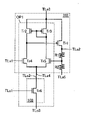
図1は、本発明の一態様の半導体装置の一例を示したブロック図である。半導体装置100は、配線REFLから参照電位が入力されることによって、配線OUTLから参照電位に応じた電位を出力するボルテージレギュレータである。半導体装置100は、回路101と、調整回路102と、回路103と、回路104と、保持回路SH1と、保持回路SH2と、を有する。
次に、回路101及び回路103の回路構成について説明する。図2は、回路101及び回路103の回路構成の例を示した図である。
次に、調整回路102の回路構成について説明する。図3(A)は、調整回路102の回路構成の例を示した図である。
次に、回路103及び回路104の回路構成について説明する。図5は、回路103及び回路104の回路構成の例を示した図である。なお、回路103及び回路104の接続構成を説明するため、図5では、調整回路102及び保持回路SH2も図示している。
次に、本発明の一態様の半導体装置の動作例について説明する。なお、本動作例では、図6に示す半導体装置100Aの動作について説明する。
初めに、調整回路102を駆動しない場合(図7(A))の、半導体装置100Aの動作例について説明する。
時刻T01より前において、配線SW1L及び配線SW2Lには、低レベル電位が印加されている。そのため、保持回路SH1に含まれるトランジスタOTr1のゲートに低レベル電位が印加されるため、トランジスタOTr1はオフ状態となる。加えて、保持回路SH2に含まれるトランジスタOTr2のゲートに低レベル電位が印加されるため、トランジスタOTr2もオフ状態となる。
時刻T01から時刻T02までの間において、配線SW2Lには、高レベル電位が印加される。そのため、保持回路SH2に含まれるトランジスタOTr2のゲートに高レベル電位が印加されるため、トランジスタOTr2はオン状態となる。
時刻T02から時刻T03までの間において、半導体装置100Aには、配線REFLから参照電位としてVREFが与えられる。
時刻T03から時刻T04までの間において、配線SW1Lには、高レベル電位が印加される。そのため、保持回路SH1に含まれるトランジスタOTr1のゲートに高レベル電位が印加されるため、トランジスタOTr1はオン状態となる。
時刻T04から時刻T05までの間において、配線REFLの電位はVREFからVG NDに変動したとする。
次に、調整回路102を駆動する場合(図7(B))の、半導体装置100Aの動作例について説明する。
時刻T11より前の半導体装置100Aの動作については、図7(A)のタイミングチャートの時刻T01より前の動作の説明を参酌する。
時刻T11から時刻T12までの間の半導体装置100Aの動作については、図7(A)のタイミングチャートの時刻T01から時刻T02までの間の動作の説明を参酌する。
時刻T12から時刻T13までの間の半導体装置100Aの動作については、図7(A)のタイミングチャートの時刻T02から時刻T03までの間の動作の説明を参酌する。
時刻T13から時刻T14までの間において、配線ADJL[1]には、任意の正の電位としてVADJが印加される。そのため、調整回路102のバッファ回路BUF[1]の入力端子にVADJが入力されて、バッファ回路BUF[1]の出力端子からVADJが出力される。これにより、調整回路102に含まれる容量素子C3[1]の第2端子にVADJが書き込まれる。
時刻T14から時刻T15までの間の半導体装置100Aの動作については、図7(A)のタイミングチャートの時刻T03から時刻T04までの間の動作と同様に行われる。
時刻T15から時刻T16までの間の半導体装置100Aの動作については、図7(A)のタイミングチャートの時刻T04から時刻T05までの間の動作の説明を参酌する。
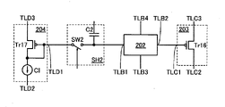
本実施の形態では、実施の形態1で説明した半導体装置100(半導体装置100A)の別の構成例について、説明する。
次に、回路201及び回路203の回路構成について説明する。図9は、回路201及び回路203の回路構成の例を示した図である。
調整回路202としては、実施の形態1で説明した、図3に示す調整回路102を適用することができる。この場合、端子TLB1乃至端子TLB4のそれぞれは、端子TLb1乃至端子TLb4に対応する。
次に、回路203及び回路204の回路構成について説明する。図10は、回路203及び回路204の回路構成の例を示した図である。なお、回路203及び回路204の接続構成を説明するため、図10では、調整回路202及び保持回路SH2も図示している。
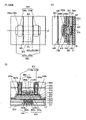
本実施の形態では、実施の形態1で説明した半導体装置100、半導体装置100A、実施の形態2で説明した半導体装置200などの断面構成例について説明する。なお、本実施の形態では、半導体装置100、半導体装置100A、実施の形態2で説明した半導体装置200などを包括して、半導体装置300と呼称する。
図12に、半導体装置300の一部の断面を示す。図12に示す半導体装置300は、基板231上に、層310および層320を積層している。図12では、基板231として単結晶半導体基板(例えば、単結晶シリコン基板)を用いる場合を示している。
図12において、層310は、基板231上にトランジスタ233a、トランジスタ233b、およびトランジスタ233cを有する。図12では、トランジスタ233a、トランジスタ233b、およびトランジスタ233cのチャネル長方向の断面を示している。
層320は、層310上に設けられる。層320は、トランジスタ368a、トランジスタ368b、容量素子369a、および容量素子369bを有する。図12では、トランジスタ368aおよびトランジスタ368bのチャネル長方向の断面を示している。なお、トランジスタ368a、およびトランジスタ368bは、バックゲートを有するトランジスタである。
〔基板〕
基板として用いる材料に大きな制限はないが、少なくとも後の加熱処理に耐えうる程度の耐熱性を有していることが必要となる。例えば、基板としてシリコンや炭化シリコンなどを材料とした単結晶半導体基板、多結晶半導体基板、シリコンゲルマニウムなどを材料とした化合物半導体基板等を用いることができる。また、SOI基板や、半導体基板上に歪トランジスタやFIN型トランジスタなどの半導体素子が設けられたものなどを用いることもできる。または、高電子移動度トランジスタ(HEMT:High Electron Mobility Transistor)に適用可能なヒ化ガリウム、ヒ化アルミニウムガリウム、ヒ化インジウムガリウム、窒化ガリウム、リン化インジウム、シリコンゲルマニウムなどを用いてもよい。すなわち、基板は、単なる支持基板に限らず、他のトランジスタなどのデバイスが形成された基板であってもよい。
絶縁層は、窒化アルミニウム、酸化アルミニウム、窒化酸化アルミニウム、酸化窒化アルミニウム、酸化マグネシウム、窒化シリコン、酸化シリコン、窒化酸化シリコン、酸化窒化シリコン、酸化ガリウム、酸化ゲルマニウム、酸化イットリウム、酸化ジルコニウム、酸化ランタン、酸化ネオジム、酸化ハフニウム、酸化タンタル、アルミニウムシリケートなどから選ばれた材料を、単層でまたは積層して用いる。また、酸化物材料、窒化物材料、酸化窒化物材料、窒化酸化物材料のうち、複数の材料を混合した材料を用いてもよい。
Ion Mass Spectrometry)において2×10²⁰atoms/cm3以下、好ましくは5×1019atoms/cm3以下、より好ましくは1×101 9atoms/cm3以下、さらに好ましくは5×1018atoms/cm3以下とする。特に、半導体層と接する絶縁層の水素濃度を低減することが好ましい。
電極を形成するための導電性材料としては、アルミニウム、クロム、銅、銀、金、白金、タンタル、ニッケル、チタン、モリブデン、タングステン、ハフニウム、バナジウム、ニオブ、マンガン、マグネシウム、ジルコニウム、ベリリウム、インジウムなどから選ばれた金属元素を1種以上含む材料を用いることができる。また、リン等の不純物元素を含有させた多結晶シリコンに代表される、電気伝導度が高い半導体、ニッケルシリサイドなどのシリサイドを用いてもよい。
半導体層として、単結晶半導体、多結晶半導体、微結晶半導体、または非晶質半導体などを、単体でまたは組み合わせて用いることができる。半導体材料としては、例えば、シリコンや、ゲルマニウムなどを用いることができる。また、シリコンゲルマニウム、炭化シリコン、ガリウムヒ素、酸化物半導体、窒化物半導体などの化合物半導体や、有機半導体などを用いることができる。
金属酸化物の一種である酸化物半導体は、少なくともインジウムまたは亜鉛を含むことが好ましい。特にインジウムおよび亜鉛を含むことが好ましい。また、それらに加えて、アルミニウム、ガリウム、イットリウムまたはスズなどが含まれていることが好ましい。また、ホウ素、シリコン、チタン、鉄、ニッケル、ゲルマニウム、ジルコニウム、モリブデン、ランタン、セリウム、ネオジム、ハフニウム、タンタル、タングステン、またはマグネシウムなどから選ばれた一種、または複数種が含まれていてもよい。
以下では、本発明の一態様で開示されるトランジスタに用いることができるCAC(Cloud-Aligned Composite)-OS、及びCAAC(c-axis
aligned crystalline)-OSについて説明する。
matrix composite)と呼称することもできる。
金属酸化物の一種である酸化物半導体は、単結晶酸化物半導体と、それ以外の非単結晶酸化物半導体と、に分けられる。非単結晶酸化物半導体としては、例えば、CAAC-OS、多結晶酸化物半導体、nc-OS(nanocrystalline oxide semiconductor)、擬似非晶質酸化物半導体(a-like OS:amorphous-like oxide semiconductor)および非晶質酸化物半導体などがある。
続いて、上記金属酸化物をトランジスタのチャネル形成領域に用いる場合について説明する。
ここで、金属酸化物中における各不純物の影響について説明する。
絶縁層を形成するための絶縁性材料、電極を形成するための導電性材料、または半導体層を形成するための半導体材料は、スパッタリング法、スピンコート法、CVD(Chemical Vapor Deposition)法(熱CVD法、MOCVD(Metal Organic Chemical Vapor Deposition)法、PECVD(Plasma Enhanced CVD)法、高密度プラズマCVD(High density plasma CVD)法、LPCVD(low pressure CVD)法、APCVD(atmospheric pressure CVD)法等を含む)、ALD(Atomic Layer Deposition)法、MBE(Molecular Beam Epitaxy)法、PLD(Pulsed Laser Deposition)法、ディップ法、スプレー塗布法、液滴吐出法(インクジェット法など)、または、印刷法(スクリーン印刷、オフセット印刷など)を用いて形成することができる。
本実施の形態では、上記実施の形態に示した半導体装置などに用いることができるトランジスタの構造例について説明する。
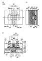
図13(A)、(B)および(C)を用いてトランジスタ510Aの構造例を説明する。図13(A)はトランジスタ510Aの上面図である。図13(B)は、図13(A)に一点鎖線L1-L2で示す部位の断面図である。図13(C)は、図13(A)に一点鎖線W1-W2で示す部位の断面図である。なお、図13(A)の上面図では、図の明瞭化のために一部の要素を省いて図示している。
図14(A)、(B)および(C)を用いてトランジスタ510Bの構造例を説明する。図14(A)はトランジスタ510Bの上面図である。図14(B)は、図14(A)に一点鎖線L1-L2で示す部位の断面図である。図14(C)は、図14(A)に一点鎖線W1-W2で示す部位の断面図である。なお、図14(A)の上面図では、図の明瞭化のために一部の要素を省いて図示している。
の拡散を抑制する機能を有する導電性材料を用いることが好ましい。
図15(A)、(B)および(C)を用いてトランジスタ510Cの構造例を説明する。図15(A)はトランジスタ510Cの上面図である。図15(B)は、図15(A)に一点鎖線L1-L2で示す部位の断面図である。図15(C)は、図15(A)に一点鎖線W1-W2で示す部位の断面図である。なお、図15(A)の上面図では、図の明瞭化のために一部の要素を省いて図示している。
図16(A)、(B)および(C)を用いてトランジスタ510Dの構造例を説明する。図16(A)はトランジスタ510Dの上面図である。図16(B)は、図16(A)に一点鎖線L1-L2で示す部位の断面図である。図16(C)は、図16(A)に一点鎖線W1-W2で示す部位の断面図である。なお、図16(A)の上面図では、図の明瞭化のために一部の要素を省いて図示している。
本実施の形態は、上記実施の形態に示す半導体装置などが組み込まれた電子部品および電子機器の一例を示す。
まず、半導体装置300が組み込まれた電子部品の例を、図17(A)、(B)を用いて説明を行う。
Package)を適用しているが、パッケージの態様はこれに限定されない。
本実施の形態では、上述の実施の形態で説明した半導体装置、又は電子部品を電子機器に適用した製品例について説明する。
本発明の一態様の半導体装置、又は電子部品は、情報端末装置に備えられるディスプレイに適用することができる。図18(A)は、情報端末装置の一種であるノート型パーソナルコンピュータであり、筐体5401、表示部5402、キーボード5403、ポインティングデバイス5404等を有する。
本発明の一態様の半導体装置、又は電子部品は、ウェアラブル端末に適用することができる。図18(B)はウェアラブル端末の一種であるスマートウォッチであり、筐体5901、表示部5902、操作ボタン5903、操作子5904、バンド5905などを有する。また、表示部5902に、位置入力装置としての機能が付加された表示装置を用いるようにしてもよい。また、位置入力装置としての機能は、表示装置にタッチパネルを設けることで付加することができる。あるいは、位置入力装置としての機能は、フォトセンサとも呼ばれる光電変換素子を表示装置の画素部に設けることでも、付加することができる。また、操作ボタン5903にスマートウォッチを起動する電源スイッチ、スマートウォッチのアプリケーションを操作するボタン、音量調整ボタン、または表示部5902を点灯、あるいは消灯するスイッチなどのいずれかを備えることができる。また、図18(B)に示したスマートウォッチでは、操作ボタン5903の数を2個示しているが、スマートウォッチの有する操作ボタンの数は、これに限定されない。また、操作子5904は、スマートウォッチの時刻合わせを行うリューズとして機能する。また、操作子5904は、時刻合わせ以外に、スマートウォッチのアプリケーションを操作する入力インターフェースとして、用いるようにしてもよい。なお、図18(B)に示したスマートウォッチでは、操作子5904を有する構成となっているが、これに限定せず、操作子5904を有さない構成であってもよい。
本発明の一態様の半導体装置、又は電子部品は、ビデオカメラに適用することができる。図18(C)に示すビデオカメラは、第1筐体5801、第2筐体5802、表示部5803、操作キー5804、レンズ5805、接続部5806等を有する。操作キー5804及びレンズ5805は第1筐体5801に設けられており、表示部5803は第2筐体5802に設けられている。そして、第1筐体5801と第2筐体5802とは、接続部5806により接続されており、第1筐体5801と第2筐体5802の間の角度は、接続部5806により変更が可能である。表示部5803における映像を、接続部5806における第1筐体5801と第2筐体5802との間の角度に従って切り替える構成としてもよい。
本発明の一態様の半導体装置、又は電子部品は、携帯電話に適用することができる。図18(D)は、情報端末の機能を有する携帯電話であり、筐体5501、表示部5502、マイク5503、スピーカ5504、操作ボタン5505を有する。また、表示部5502に、位置入力装置としての機能が付加された表示装置を用いるようにしてもよい。また、位置入力装置としての機能は、表示装置にタッチパネルを設けることで付加することができる。あるいは、位置入力装置としての機能は、フォトセンサとも呼ばれる光電変換素子を表示装置の画素部に設けることでも、付加することができる。また、操作ボタン5505に携帯電話を起動する電源スイッチ、携帯電話のアプリケーションを操作するボタン、音量調整ボタン、または表示部5502を点灯、あるいは消灯するスイッチなどのいずれかを備えることができる。
本発明の一態様の半導体装置、又は電子部品は、テレビジョン装置に適用することができる。図18(E)に示すテレビジョン装置は、筐体9000、表示部9001、スピーカ9003、操作キー9005(電源スイッチ、または操作スイッチを含む)、接続端子9006などを有する。テレビジョン装置は、大画面、例えば、50インチ以上、または100インチ以上の表示部9001を組み込むことが可能である。
本発明の一態様の半導体装置、又は電子部品は、移動体である自動車の運転席周辺に適用することができる。
本発明の一態様の半導体装置、又は電子部品は、据え置き型ゲーム機、又は携帯型ゲーム機に適用することができる。図18(G)には据え置き型ゲーム機を示しており、ゲーム機本体7520と、無線または有線で接続することができるコントローラ7522と、が図示されている。また、図18(H)には携帯型ゲーム機を示しており、携帯型ゲーム機は、筐体5201と、表示部5202と、ボタン5203と、を有する。
本明細書に記載の実施の形態、及び実施例における各構成の説明について、以下に付記する。
各実施の形態、及び実施例に示す構成は、他の実施の形態に示す構成と適宜組み合わせて、本発明の一態様とすることができる。また、1つの実施の形態の中に、複数の構成例が示される場合は、互いに構成例を適宜組み合わせることが可能である。
本明細書等において、「第1」、「第2」、「第3」という序数詞は、構成要素の混同を避けるために付したものである。従って、構成要素の数を限定するものではない。また、構成要素の順序を限定するものではない。また例えば、本明細書等の実施の形態(又は実施例)の一において「第1」に言及された構成要素が、他の実施の形態(又は実施例)、あるいは特許請求の範囲において「第2」に言及された構成要素とすることもありうる。また例えば、本明細書等の実施の形態(又は実施例)の一において「第1」に言及された構成要素を、他の実施の形態、あるいは特許請求の範囲において省略することもありうる。
実施の形態(又は実施例)について図面を参照しながら説明している。但し、実施の形態(又は実施例)は多くの異なる態様で実施することが可能であり、趣旨及びその範囲から逸脱することなく、その形態及び詳細を様々に変更し得ることは当業者であれば容易に理解される。従って、本発明は、実施の形態(又は実施例)の記載内容に限定して解釈されるものではない。なお、実施の形態の発明の構成(又は実施例の構成)において、同一部分又は同様な機能を有する部分には同一の符号を異なる図面間で共通して用い、その繰り返しの説明は省略する。
本明細書等において、トランジスタの接続関係を説明する際、「ソース又はドレインの一方」(又は第1電極、又は第1端子)、「ソース又はドレインの他方」(又は第2電極、又は第2端子)という表記を用いる。これは、トランジスタのソースとドレインは、トランジスタの構造又は動作条件等によって変わるためである。なおトランジスタのソースとドレインの呼称については、ソース(ドレイン)端子や、ソース(ドレイン)電極等、状況に応じて適切に言い換えることができる。また、本明細書等では、ゲート以外の2つの端子を第1端子、第2端子と呼ぶ場合や、第3端子、第4端子と呼ぶ場合がある。なお、本明細書等において、チャネル形成領域はチャネルが形成される領域を指し、ゲートに電位を印加することでこの領域が形成されて、ソース‐ドレイン間に電流を流すことができる。
以下では、上記実施の形態、及び実施例で言及した語句の定義について説明する。
半導体の不純物とは、例えば、半導体層を構成する主成分以外をいう。例えば、濃度が0.1原子%未満の元素は不純物である。不純物が含まれることにより、例えば、半導体にDOS(Density of States)が形成されることや、キャリア移動度が低下することや、結晶性が低下することなどが起こる場合がある。半導体が酸化物半導体である場合、半導体の特性を変化させる不純物としては、例えば、第1族元素、第2族元素、第13族元素、第14族元素、第15族元素、主成分以外の遷移金属などがあり、特に、例えば、水素(水にも含まれる)、リチウム、ナトリウム、シリコン、ホウ素、リン、炭素、窒素などがある。酸化物半導体の場合、例えば水素などの不純物の混入によって酸素欠損を形成する場合がある。また、半導体がシリコン層である場合、半導体の特性を変化させる不純物としては、例えば、酸素、水素を除く第1族元素、第2族元素、第13族元素、第15族元素などがある。
本明細書等において、スイッチとは、導通状態(オン状態)、又は、非導通状態(オフ状態)になり、電流を流すか流さないかを制御する機能を有するものをいう。又は、スイッチとは、電流を流す経路を選択して切り替える機能を有するものをいう。
本明細書等において、XとYとが接続されている、と記載する場合は、XとYとが電気的に接続されている場合と、XとYとが機能的に接続されている場合と、XとYとが直接接続されている場合とを含むものとする。したがって、所定の接続関係、例えば、図又は文章に示された接続関係に限定されず、図又は文章に示された接続関係以外のものも含むものとする。
Claims (11)
- 第1回路、第2回路、及び第3回路と、第1保持回路と、を有し、
前記第1保持回路は、第1保持部を有し、
前記第1保持回路は、前記第1保持部を電気的に浮遊状態にして、前記第1保持部の第1電位を保持する機能を有し、
前記第1回路は、前記第1保持部の前記第1電位を第2電位に変動する機能を有し、
前記第2回路は、前記第1保持部の前記第1電位、又は前記第2電位に基づくバイアス電流を生成する機能を有し、
前記第3回路は、第1端子、第2端子、及び第3端子と、を有し、
前記第3回路は、前記バイアス電流が前記第3回路の前記第1端子に供給されることで、前記第3回路の前記第2端子への入力電位に応じて第3電位を生成して、前記第3回路の前記第3端子から前記第3電位を出力する機能を有する半導体装置。 - 請求項1において、
前記第1回路は、第1容量素子を有し、
前記第1容量素子の第1端子は、前記第1保持部に電気的に接続され、
前記第1回路は、前記第1保持回路が前記第1保持部を電気的に浮遊状態にした後に、前記第1容量素子の第2端子に第4電位が入力されることで、前記第1容量素子の容量結合によって前記第1保持部に保持されている前記第1電位を前記第2電位に変動する機能を有する半導体装置。 - 請求項2において、
前記第1回路は、バッファ回路を有し、
前記バッファ回路の出力端子は、前記第1容量素子の前記第2端子に電気的に接続されている半導体装置。 - 請求項2において、
前記第1回路は、マルチプレクサを有し、
前記マルチプレクサの出力端子は、前記第1容量素子の前記第2端子に電気的に接続されている半導体装置。 - 請求項2において、
前記第1回路は、コンパレータを有し、
前記コンパレータの出力端子は、前記第1容量素子の前記第2端子に電気的に接続され、
前記コンパレータの第1入力端子には前記第3電位が入力され、
前記コンパレータの第2入力端子には第5電位が入力されている半導体装置。 - 請求項1乃至請求項5のいずれか一において、
前記第1保持回路は、第1トランジスタと、第2容量素子と、を有し、
前記第1保持部は、前記第1トランジスタの第1端子と、前記第2容量素子の第1端子と、に電気的に接続され、
前記第1トランジスタは、チャネル形成領域に金属酸化物を有する半導体装置。 - 請求項6において、
第4回路を有し、
前記第4回路は、定電流を流す機能を有し、
前記第4回路は、前記第1トランジスタの第2端子に電気的に接続され、
前記第1トランジスタが導通状態のとき、前記第1トランジスタの前記第1端子には、前記定電流に応じた前記第1電位が入力される半導体装置。 - 請求項1乃至請求項7のいずれか一において、
第2保持回路を有し、
前記第2保持回路は、第2保持部を有し、
前記第2保持部は、前記第3回路の前記第2端子に電気的に接続され、
前記第2保持回路は、前記第2保持部を電気的に浮遊状態にして、前記第3回路の前記第2端子への前記入力電位を保持する機能を有する半導体装置。 - 請求項8において、
前記第2保持回路は、第2トランジスタと、第3容量素子と、を有し、
前記第2保持部は、前記第2トランジスタの第1端子と、前記第3容量素子の第1端子と、に電気的に接続され、
前記第2トランジスタの第2端子には、前記入力電位が入力され、
前記第2トランジスタは、チャネル形成領域に金属酸化物を有する半導体装置。 - 請求項1乃至請求項9のいずれか一の半導体装置と、集積回路と、がプリント基板上に設けられている電子部品。
- 請求項1乃至請求項9のいずれか一の半導体装置と、筐体と、を有する電子機器。
Applications Claiming Priority (3)
| Application Number | Priority Date | Filing Date | Title |
|---|---|---|---|
| JP2018009327 | 2018-01-24 | ||
| JP2018009327 | 2018-01-24 | ||
| PCT/IB2019/050173 WO2019145803A1 (ja) | 2018-01-24 | 2019-01-10 | 半導体装置、電子部品、及び電子機器 |
Publications (2)
| Publication Number | Publication Date |
|---|---|
| JPWO2019145803A1 JPWO2019145803A1 (ja) | 2021-03-04 |
| JP7204686B2 true JP7204686B2 (ja) | 2023-01-16 |
Family
ID=67395345
Family Applications (1)
| Application Number | Title | Priority Date | Filing Date |
|---|---|---|---|
| JP2019567410A Active JP7204686B2 (ja) | 2018-01-24 | 2019-01-10 | 半導体装置、電子部品、及び電子機器 |
Country Status (5)
| Country | Link |
|---|---|
| US (1) | US11714438B2 (ja) |
| JP (1) | JP7204686B2 (ja) |
| KR (1) | KR102605008B1 (ja) |
| CN (1) | CN112041776B (ja) |
| WO (1) | WO2019145803A1 (ja) |
Families Citing this family (5)
| Publication number | Priority date | Publication date | Assignee | Title |
|---|---|---|---|---|
| US11663990B2 (en) | 2018-11-09 | 2023-05-30 | Semiconductor Energy Laboratory Co., Ltd. | Display apparatus and electronic device |
| JP7777531B2 (ja) * | 2020-08-19 | 2025-11-28 | 株式会社半導体エネルギー研究所 | ハフニウムジルコニウム酸化物の製造方法 |
| US11942468B2 (en) * | 2021-05-25 | 2024-03-26 | Cirrus Logic, Inc. | Symmetric layout for high-voltage amplifier |
| TWI802096B (zh) * | 2021-11-23 | 2023-05-11 | 新唐科技股份有限公司 | 電晶體元件 |
| CN119559913B (zh) * | 2024-12-23 | 2025-10-28 | 上海天马微电子有限公司 | 一种显示面板及其控制方法、显示装置 |
Citations (3)
| Publication number | Priority date | Publication date | Assignee | Title |
|---|---|---|---|---|
| JP2005196251A (ja) | 2003-12-26 | 2005-07-21 | Ricoh Co Ltd | 定電圧回路 |
| JP2007184688A (ja) | 2006-01-04 | 2007-07-19 | Fujitsu Ltd | バイアス回路 |
| JP2013235564A (ja) | 2012-04-11 | 2013-11-21 | Semiconductor Energy Lab Co Ltd | 半導体装置 |
Family Cites Families (109)
| Publication number | Priority date | Publication date | Assignee | Title |
|---|---|---|---|---|
| US5159260A (en) | 1978-03-08 | 1992-10-27 | Hitachi, Ltd. | Reference voltage generator device |
| US4553098A (en) | 1978-04-05 | 1985-11-12 | Hitachi, Ltd. | Battery checker |
| US4559694A (en) | 1978-09-13 | 1985-12-24 | Hitachi, Ltd. | Method of manufacturing a reference voltage generator device |
| KR940017214A (ko) | 1992-12-24 | 1994-07-26 | 가나이 쓰토무 | 기준전압 발생회로 |
| DE69635107D1 (de) | 1995-08-03 | 2005-09-29 | Koninkl Philips Electronics Nv | Halbleiteranordnung mit einem transparenten schaltungselement |
| JP3625598B2 (ja) | 1995-12-30 | 2005-03-02 | 三星電子株式会社 | 液晶表示装置の製造方法 |
| JP2000150861A (ja) | 1998-11-16 | 2000-05-30 | Tdk Corp | 酸化物薄膜 |
| JP3276930B2 (ja) | 1998-11-17 | 2002-04-22 | 科学技術振興事業団 | トランジスタ及び半導体装置 |
| US6114907A (en) | 1998-12-08 | 2000-09-05 | National Semiconductor Corporation | Amplifier with dynamic compensation and method |
| TW460731B (en) | 1999-09-03 | 2001-10-21 | Ind Tech Res Inst | Electrode structure and production method of wide viewing angle LCD |
| US6785344B1 (en) * | 2000-04-11 | 2004-08-31 | Terawave Communications, Inc. | Fast threshold determination for packet-multiplexed digital communication |
| KR20020038482A (ko) | 2000-11-15 | 2002-05-23 | 모리시타 요이찌 | 박막 트랜지스터 어레이, 그 제조방법 및 그것을 이용한표시패널 |
| JP3997731B2 (ja) | 2001-03-19 | 2007-10-24 | 富士ゼロックス株式会社 | 基材上に結晶性半導体薄膜を形成する方法 |
| US6518817B2 (en) * | 2001-06-28 | 2003-02-11 | Intel Corporation | Voltage buffer |
| JP4090716B2 (ja) | 2001-09-10 | 2008-05-28 | 雅司 川崎 | 薄膜トランジスタおよびマトリクス表示装置 |
| EP1443130B1 (en) | 2001-11-05 | 2011-09-28 | Japan Science and Technology Agency | Natural superlattice homologous single crystal thin film, method for preparation thereof, and device using said single crystal thin film |
| JP2003283271A (ja) | 2002-01-17 | 2003-10-03 | Semiconductor Energy Lab Co Ltd | 電気回路 |
| JP4083486B2 (ja) | 2002-02-21 | 2008-04-30 | 独立行政法人科学技術振興機構 | LnCuO(S,Se,Te)単結晶薄膜の製造方法 |
| US7049190B2 (en) | 2002-03-15 | 2006-05-23 | Sanyo Electric Co., Ltd. | Method for forming ZnO film, method for forming ZnO semiconductor layer, method for fabricating semiconductor device, and semiconductor device |
| JP3933591B2 (ja) | 2002-03-26 | 2007-06-20 | 淳二 城戸 | 有機エレクトロルミネッセント素子 |
| US7339187B2 (en) | 2002-05-21 | 2008-03-04 | State Of Oregon Acting By And Through The Oregon State Board Of Higher Education On Behalf Of Oregon State University | Transistor structures |
| JP2004022625A (ja) | 2002-06-13 | 2004-01-22 | Murata Mfg Co Ltd | 半導体デバイス及び該半導体デバイスの製造方法 |
| JP2004022093A (ja) * | 2002-06-18 | 2004-01-22 | Toshiba Corp | 半導体記憶装置 |
| US7105868B2 (en) | 2002-06-24 | 2006-09-12 | Cermet, Inc. | High-electron mobility transistor with zinc oxide |
| US7067843B2 (en) | 2002-10-11 | 2006-06-27 | E. I. Du Pont De Nemours And Company | Transparent oxide semiconductor thin film transistors |
| JP4108633B2 (ja) | 2003-06-20 | 2008-06-25 | シャープ株式会社 | 薄膜トランジスタおよびその製造方法ならびに電子デバイス |
| US7262463B2 (en) | 2003-07-25 | 2007-08-28 | Hewlett-Packard Development Company, L.P. | Transistor including a deposited channel region having a doped portion |
| JP4445780B2 (ja) | 2004-03-02 | 2010-04-07 | Okiセミコンダクタ株式会社 | 電圧レギュレータ |
| EP1737044B1 (en) | 2004-03-12 | 2014-12-10 | Japan Science and Technology Agency | Amorphous oxide and thin film transistor |
| US7297977B2 (en) | 2004-03-12 | 2007-11-20 | Hewlett-Packard Development Company, L.P. | Semiconductor device |
| US7145174B2 (en) | 2004-03-12 | 2006-12-05 | Hewlett-Packard Development Company, Lp. | Semiconductor device |
| US7282782B2 (en) | 2004-03-12 | 2007-10-16 | Hewlett-Packard Development Company, L.P. | Combined binary oxide semiconductor device |
| CN102176237B (zh) | 2004-04-09 | 2015-09-30 | 株式会社半导体能源研究所 | 限幅器以及采用限幅器的半导体器件 |
| US7211825B2 (en) | 2004-06-14 | 2007-05-01 | Yi-Chi Shih | Indium oxide-based thin film transistors and circuits |
| US7531852B2 (en) | 2004-06-14 | 2009-05-12 | Denso Corporation | Electronic unit with a substrate where an electronic circuit is fabricated |
| JP2006100760A (ja) | 2004-09-02 | 2006-04-13 | Casio Comput Co Ltd | 薄膜トランジスタおよびその製造方法 |
| US7285501B2 (en) | 2004-09-17 | 2007-10-23 | Hewlett-Packard Development Company, L.P. | Method of forming a solution processed device |
| US7298084B2 (en) | 2004-11-02 | 2007-11-20 | 3M Innovative Properties Company | Methods and displays utilizing integrated zinc oxide row and column drivers in conjunction with organic light emitting diodes |
| US7453065B2 (en) | 2004-11-10 | 2008-11-18 | Canon Kabushiki Kaisha | Sensor and image pickup device |
| US7579224B2 (en) | 2005-01-21 | 2009-08-25 | Semiconductor Energy Laboratory Co., Ltd. | Method for manufacturing a thin film semiconductor device |
| TWI562380B (en) | 2005-01-28 | 2016-12-11 | Semiconductor Energy Lab Co Ltd | Semiconductor device, electronic device, and method of manufacturing semiconductor device |
| TWI569441B (zh) | 2005-01-28 | 2017-02-01 | 半導體能源研究所股份有限公司 | 半導體裝置,電子裝置,和半導體裝置的製造方法 |
| US7858451B2 (en) | 2005-02-03 | 2010-12-28 | Semiconductor Energy Laboratory Co., Ltd. | Electronic device, semiconductor device and manufacturing method thereof |
| US7948171B2 (en) | 2005-02-18 | 2011-05-24 | Semiconductor Energy Laboratory Co., Ltd. | Light emitting device |
| US20060197092A1 (en) | 2005-03-03 | 2006-09-07 | Randy Hoffman | System and method for forming conductive material on a substrate |
| US8681077B2 (en) | 2005-03-18 | 2014-03-25 | Semiconductor Energy Laboratory Co., Ltd. | Semiconductor device, and display device, driving method and electronic apparatus thereof |
| US7068019B1 (en) * | 2005-03-23 | 2006-06-27 | Mediatek Inc. | Switchable linear regulator |
| US7544967B2 (en) | 2005-03-28 | 2009-06-09 | Massachusetts Institute Of Technology | Low voltage flexible organic/transparent transistor for selective gas sensing, photodetecting and CMOS device applications |
| US7645478B2 (en) | 2005-03-31 | 2010-01-12 | 3M Innovative Properties Company | Methods of making displays |
| US8300031B2 (en) | 2005-04-20 | 2012-10-30 | Semiconductor Energy Laboratory Co., Ltd. | Semiconductor device comprising transistor having gate and drain connected through a current-voltage conversion element |
| JP2006344849A (ja) | 2005-06-10 | 2006-12-21 | Casio Comput Co Ltd | 薄膜トランジスタ |
| US7691666B2 (en) | 2005-06-16 | 2010-04-06 | Eastman Kodak Company | Methods of making thin film transistors comprising zinc-oxide-based semiconductor materials and transistors made thereby |
| US7402506B2 (en) | 2005-06-16 | 2008-07-22 | Eastman Kodak Company | Methods of making thin film transistors comprising zinc-oxide-based semiconductor materials and transistors made thereby |
| US7507618B2 (en) | 2005-06-27 | 2009-03-24 | 3M Innovative Properties Company | Method for making electronic devices using metal oxide nanoparticles |
| KR100711890B1 (ko) | 2005-07-28 | 2007-04-25 | 삼성에스디아이 주식회사 | 유기 발광표시장치 및 그의 제조방법 |
| JP2007059128A (ja) | 2005-08-23 | 2007-03-08 | Canon Inc | 有機el表示装置およびその製造方法 |
| JP2007073705A (ja) | 2005-09-06 | 2007-03-22 | Canon Inc | 酸化物半導体チャネル薄膜トランジスタおよびその製造方法 |
| JP4280736B2 (ja) | 2005-09-06 | 2009-06-17 | キヤノン株式会社 | 半導体素子 |
| JP4850457B2 (ja) | 2005-09-06 | 2012-01-11 | キヤノン株式会社 | 薄膜トランジスタ及び薄膜ダイオード |
| JP5116225B2 (ja) | 2005-09-06 | 2013-01-09 | キヤノン株式会社 | 酸化物半導体デバイスの製造方法 |
| EP3614442A3 (en) | 2005-09-29 | 2020-03-25 | Semiconductor Energy Laboratory Co., Ltd. | Semiconductor device having oxide semiconductor layer and manufactoring method thereof |
| JP5037808B2 (ja) | 2005-10-20 | 2012-10-03 | キヤノン株式会社 | アモルファス酸化物を用いた電界効果型トランジスタ、及び該トランジスタを用いた表示装置 |
| KR101117948B1 (ko) | 2005-11-15 | 2012-02-15 | 가부시키가이샤 한도오따이 에네루기 켄큐쇼 | 액정 디스플레이 장치 제조 방법 |
| US7432737B2 (en) | 2005-12-28 | 2008-10-07 | Semiconductor Energy Laboratory Co., Ltd. | Semiconductor device, display device, and electronic device |
| TWI292281B (en) | 2005-12-29 | 2008-01-01 | Ind Tech Res Inst | Pixel structure of active organic light emitting diode and method of fabricating the same |
| US7867636B2 (en) | 2006-01-11 | 2011-01-11 | Murata Manufacturing Co., Ltd. | Transparent conductive film and method for manufacturing the same |
| JP4977478B2 (ja) | 2006-01-21 | 2012-07-18 | 三星電子株式会社 | ZnOフィルム及びこれを用いたTFTの製造方法 |
| US7576394B2 (en) | 2006-02-02 | 2009-08-18 | Kochi Industrial Promotion Center | Thin film transistor including low resistance conductive thin films and manufacturing method thereof |
| US7977169B2 (en) | 2006-02-15 | 2011-07-12 | Kochi Industrial Promotion Center | Semiconductor device including active layer made of zinc oxide with controlled orientations and manufacturing method thereof |
| JP4804975B2 (ja) | 2006-03-22 | 2011-11-02 | エルピーダメモリ株式会社 | 基準電位発生回路及びそれを備えた半導体記憶装置 |
| KR20070101595A (ko) | 2006-04-11 | 2007-10-17 | 삼성전자주식회사 | ZnO TFT |
| US20070252928A1 (en) | 2006-04-28 | 2007-11-01 | Toppan Printing Co., Ltd. | Structure, transmission type liquid crystal display, reflection type display and manufacturing method thereof |
| JP5028033B2 (ja) | 2006-06-13 | 2012-09-19 | キヤノン株式会社 | 酸化物半導体膜のドライエッチング方法 |
| JP4609797B2 (ja) | 2006-08-09 | 2011-01-12 | Nec液晶テクノロジー株式会社 | 薄膜デバイス及びその製造方法 |
| JP4999400B2 (ja) | 2006-08-09 | 2012-08-15 | キヤノン株式会社 | 酸化物半導体膜のドライエッチング方法 |
| JP4332545B2 (ja) | 2006-09-15 | 2009-09-16 | キヤノン株式会社 | 電界効果型トランジスタ及びその製造方法 |
| JP5164357B2 (ja) | 2006-09-27 | 2013-03-21 | キヤノン株式会社 | 半導体装置及び半導体装置の製造方法 |
| JP4274219B2 (ja) | 2006-09-27 | 2009-06-03 | セイコーエプソン株式会社 | 電子デバイス、有機エレクトロルミネッセンス装置、有機薄膜半導体装置 |
| US7622371B2 (en) | 2006-10-10 | 2009-11-24 | Hewlett-Packard Development Company, L.P. | Fused nanocrystal thin film semiconductor and method |
| US7772021B2 (en) | 2006-11-29 | 2010-08-10 | Samsung Electronics Co., Ltd. | Flat panel displays comprising a thin-film transistor having a semiconductive oxide in its channel and methods of fabricating the same for use in flat panel displays |
| JP2008140684A (ja) | 2006-12-04 | 2008-06-19 | Toppan Printing Co Ltd | カラーelディスプレイおよびその製造方法 |
| KR101303578B1 (ko) | 2007-01-05 | 2013-09-09 | 삼성전자주식회사 | 박막 식각 방법 |
| US8207063B2 (en) | 2007-01-26 | 2012-06-26 | Eastman Kodak Company | Process for atomic layer deposition |
| TWI331335B (en) * | 2007-03-06 | 2010-10-01 | Nanya Technology Corp | Semiconductor device and the related semiconductor memory module and signal adjustment method |
| KR100851215B1 (ko) | 2007-03-14 | 2008-08-07 | 삼성에스디아이 주식회사 | 박막 트랜지스터 및 이를 이용한 유기 전계 발광표시장치 |
| US7795613B2 (en) | 2007-04-17 | 2010-09-14 | Toppan Printing Co., Ltd. | Structure with transistor |
| KR101325053B1 (ko) | 2007-04-18 | 2013-11-05 | 삼성디스플레이 주식회사 | 박막 트랜지스터 기판 및 이의 제조 방법 |
| KR20080094300A (ko) | 2007-04-19 | 2008-10-23 | 삼성전자주식회사 | 박막 트랜지스터 및 그 제조 방법과 박막 트랜지스터를포함하는 평판 디스플레이 |
| KR101334181B1 (ko) | 2007-04-20 | 2013-11-28 | 삼성전자주식회사 | 선택적으로 결정화된 채널층을 갖는 박막 트랜지스터 및 그제조 방법 |
| CN101663762B (zh) | 2007-04-25 | 2011-09-21 | 佳能株式会社 | 氧氮化物半导体 |
| KR101345376B1 (ko) | 2007-05-29 | 2013-12-24 | 삼성전자주식회사 | ZnO 계 박막 트랜지스터 및 그 제조방법 |
| CN101878460A (zh) | 2007-11-30 | 2010-11-03 | Nxp股份有限公司 | 用于提供参考电压的装置和方法 |
| US8202365B2 (en) | 2007-12-17 | 2012-06-19 | Fujifilm Corporation | Process for producing oriented inorganic crystalline film, and semiconductor device using the oriented inorganic crystalline film |
| JP2009171548A (ja) | 2007-12-20 | 2009-07-30 | Nec Electronics Corp | 差動増幅回路 |
| US8138742B2 (en) | 2008-02-06 | 2012-03-20 | Mediatek Inc. | Semiconductor circuits capable of mitigating unwanted effects caused by input signal variations |
| JP4623179B2 (ja) | 2008-09-18 | 2011-02-02 | ソニー株式会社 | 薄膜トランジスタおよびその製造方法 |
| WO2010038602A1 (en) | 2008-10-02 | 2010-04-08 | Semiconductor Energy Laboratory Co., Ltd. | Semiconductor device and rfid tag using the semiconductor device |
| JP5451280B2 (ja) | 2008-10-09 | 2014-03-26 | キヤノン株式会社 | ウルツ鉱型結晶成長用基板およびその製造方法ならびに半導体装置 |
| KR101585958B1 (ko) | 2008-12-29 | 2016-01-18 | 주식회사 동부하이텍 | 기준전압 발생회로 |
| JP5467845B2 (ja) | 2009-09-29 | 2014-04-09 | セイコーインスツル株式会社 | ボルテージレギュレータ |
| KR101773641B1 (ko) | 2010-01-22 | 2017-09-12 | 가부시키가이샤 한도오따이 에네루기 켄큐쇼 | 반도체 장치 |
| US8508276B2 (en) | 2010-08-25 | 2013-08-13 | Semiconductor Energy Laboratory Co., Ltd. | Semiconductor device including latch circuit |
| JP5727892B2 (ja) | 2010-08-26 | 2015-06-03 | 株式会社半導体エネルギー研究所 | 半導体装置 |
| JP5908263B2 (ja) | 2010-12-03 | 2016-04-26 | 株式会社半導体エネルギー研究所 | Dc−dcコンバータ |
| US8400339B2 (en) * | 2011-03-30 | 2013-03-19 | Freescale Semiconductor, Inc. | Correlated-level-shifting and correlated-double-sampling switched-capacitor gain stages, systems implementing the gain stages, and methods of their operation |
| JP2013012000A (ja) * | 2011-06-29 | 2013-01-17 | Mitsumi Electric Co Ltd | レギュレータ用半導体集積回路 |
| US8542066B2 (en) | 2012-02-09 | 2013-09-24 | Analog Devices, Inc. | Apparatus and methods for reducing output noise of a signal channel |
| US9435841B2 (en) * | 2012-04-13 | 2016-09-06 | International Business Machines Corporation | Integrated circuit protection during high-current ESD testing |
| US9378844B2 (en) * | 2013-07-31 | 2016-06-28 | Semiconductor Energy Laboratory Co., Ltd. | Semiconductor device including transistor whose gate is electrically connected to capacitor |
-
2019
- 2019-01-10 JP JP2019567410A patent/JP7204686B2/ja active Active
- 2019-01-10 US US16/961,991 patent/US11714438B2/en active Active
- 2019-01-10 KR KR1020207023702A patent/KR102605008B1/ko active Active
- 2019-01-10 WO PCT/IB2019/050173 patent/WO2019145803A1/ja not_active Ceased
- 2019-01-10 CN CN201980007719.9A patent/CN112041776B/zh not_active Expired - Fee Related
Patent Citations (3)
| Publication number | Priority date | Publication date | Assignee | Title |
|---|---|---|---|---|
| JP2005196251A (ja) | 2003-12-26 | 2005-07-21 | Ricoh Co Ltd | 定電圧回路 |
| JP2007184688A (ja) | 2006-01-04 | 2007-07-19 | Fujitsu Ltd | バイアス回路 |
| JP2013235564A (ja) | 2012-04-11 | 2013-11-21 | Semiconductor Energy Lab Co Ltd | 半導体装置 |
Also Published As
| Publication number | Publication date |
|---|---|
| KR20200106544A (ko) | 2020-09-14 |
| CN112041776B (zh) | 2022-06-07 |
| WO2019145803A1 (ja) | 2019-08-01 |
| WO2019145803A8 (ja) | 2020-06-25 |
| CN112041776A (zh) | 2020-12-04 |
| KR102605008B1 (ko) | 2023-11-24 |
| US20200401170A1 (en) | 2020-12-24 |
| US11714438B2 (en) | 2023-08-01 |
| JPWO2019145803A1 (ja) | 2021-03-04 |
Similar Documents
| Publication | Publication Date | Title |
|---|---|---|
| JP7204686B2 (ja) | 半導体装置、電子部品、及び電子機器 | |
| KR102708331B1 (ko) | 디스플레이 및 상기 디스플레이를 포함하는 전자 기기 | |
| JP7615365B2 (ja) | 半導体装置 | |
| JP2017174489A (ja) | 半導体装置、半導体ウエハ、および電子機器 | |
| JP6798942B2 (ja) | トランジスタおよび半導体装置 | |
| JP2018074151A (ja) | 半導体装置 | |
| JP7642113B2 (ja) | 半導体装置 | |
| WO2018220491A1 (ja) | 半導体装置、電子部品及び電子機器 | |
| JP2025126183A (ja) | トランジスタ | |
| JP2025168376A (ja) | 発光装置 | |
| JPWO2019016642A1 (ja) | 半導体装置、および半導体装置の作製方法 | |
| JPWO2020084399A1 (ja) | 単極性レベルシフト回路、および、半導体装置 | |
| WO2021181192A1 (ja) | 半導体装置、及び電子機器 | |
| WO2020225640A1 (ja) | 半導体装置 | |
| JP7083727B2 (ja) | 半導体装置 | |
| JP2022002342A (ja) | 半導体装置 | |
| US20250132251A1 (en) | Semiconductor device |
Legal Events
| Date | Code | Title | Description |
|---|---|---|---|
| A621 | Written request for application examination |
Free format text: JAPANESE INTERMEDIATE CODE: A621 Effective date: 20220106 |
|
| TRDD | Decision of grant or rejection written | ||
| A01 | Written decision to grant a patent or to grant a registration (utility model) |
Free format text: JAPANESE INTERMEDIATE CODE: A01 Effective date: 20221206 |
|
| A61 | First payment of annual fees (during grant procedure) |
Free format text: JAPANESE INTERMEDIATE CODE: A61 Effective date: 20221228 |
|
| R150 | Certificate of patent or registration of utility model |
Ref document number: 7204686 Country of ref document: JP Free format text: JAPANESE INTERMEDIATE CODE: R150 |
|
| R250 | Receipt of annual fees |
Free format text: JAPANESE INTERMEDIATE CODE: R250 |