JP7204686B2 - Semiconductor devices, electronic components, and electronic equipment - Google Patents
Semiconductor devices, electronic components, and electronic equipment Download PDFInfo
- Publication number
- JP7204686B2 JP7204686B2 JP2019567410A JP2019567410A JP7204686B2 JP 7204686 B2 JP7204686 B2 JP 7204686B2 JP 2019567410 A JP2019567410 A JP 2019567410A JP 2019567410 A JP2019567410 A JP 2019567410A JP 7204686 B2 JP7204686 B2 JP 7204686B2
- Authority
- JP
- Japan
- Prior art keywords
- terminal
- circuit
- transistor
- potential
- oxide
- Prior art date
- Legal status (The legal status is an assumption and is not a legal conclusion. Google has not performed a legal analysis and makes no representation as to the accuracy of the status listed.)
- Active
Links
Images


Classifications
-
- G—PHYSICS
- G05—CONTROLLING; REGULATING
- G05F—SYSTEMS FOR REGULATING ELECTRIC OR MAGNETIC VARIABLES
- G05F1/00—Automatic systems in which deviations of an electric quantity from one or more predetermined values are detected at the output of the system and fed back to a device within the system to restore the detected quantity to its predetermined value or values, i.e. retroactive systems
- G05F1/10—Regulating voltage or current
- G05F1/46—Regulating voltage or current wherein the variable actually regulated by the final control device is DC
- G05F1/56—Regulating voltage or current wherein the variable actually regulated by the final control device is DC using semiconductor devices in series with the load as final control devices
-
- G—PHYSICS
- G09—EDUCATION; CRYPTOGRAPHY; DISPLAY; ADVERTISING; SEALS
- G09G—ARRANGEMENTS OR CIRCUITS FOR CONTROL OF INDICATING DEVICES USING STATIC MEANS TO PRESENT VARIABLE INFORMATION
- G09G3/00—Control arrangements or circuits, of interest only in connection with visual indicators other than cathode-ray tubes
- G09G3/20—Control arrangements or circuits, of interest only in connection with visual indicators other than cathode-ray tubes for presentation of an assembly of a number of characters, e.g. a page, by composing the assembly by combination of individual elements arranged in a matrix no fixed position being assigned to or needed to be assigned to the individual characters or partial characters
- G09G3/22—Control arrangements or circuits, of interest only in connection with visual indicators other than cathode-ray tubes for presentation of an assembly of a number of characters, e.g. a page, by composing the assembly by combination of individual elements arranged in a matrix no fixed position being assigned to or needed to be assigned to the individual characters or partial characters using controlled light sources
- G09G3/30—Control arrangements or circuits, of interest only in connection with visual indicators other than cathode-ray tubes for presentation of an assembly of a number of characters, e.g. a page, by composing the assembly by combination of individual elements arranged in a matrix no fixed position being assigned to or needed to be assigned to the individual characters or partial characters using controlled light sources using electroluminescent panels
- G09G3/32—Control arrangements or circuits, of interest only in connection with visual indicators other than cathode-ray tubes for presentation of an assembly of a number of characters, e.g. a page, by composing the assembly by combination of individual elements arranged in a matrix no fixed position being assigned to or needed to be assigned to the individual characters or partial characters using controlled light sources using electroluminescent panels semiconductive, e.g. using light-emitting diodes [LED]
- G09G3/3208—Control arrangements or circuits, of interest only in connection with visual indicators other than cathode-ray tubes for presentation of an assembly of a number of characters, e.g. a page, by composing the assembly by combination of individual elements arranged in a matrix no fixed position being assigned to or needed to be assigned to the individual characters or partial characters using controlled light sources using electroluminescent panels semiconductive, e.g. using light-emitting diodes [LED] organic, e.g. using organic light-emitting diodes [OLED]
- G09G3/3225—Control arrangements or circuits, of interest only in connection with visual indicators other than cathode-ray tubes for presentation of an assembly of a number of characters, e.g. a page, by composing the assembly by combination of individual elements arranged in a matrix no fixed position being assigned to or needed to be assigned to the individual characters or partial characters using controlled light sources using electroluminescent panels semiconductive, e.g. using light-emitting diodes [LED] organic, e.g. using organic light-emitting diodes [OLED] using an active matrix
- G09G3/3233—Control arrangements or circuits, of interest only in connection with visual indicators other than cathode-ray tubes for presentation of an assembly of a number of characters, e.g. a page, by composing the assembly by combination of individual elements arranged in a matrix no fixed position being assigned to or needed to be assigned to the individual characters or partial characters using controlled light sources using electroluminescent panels semiconductive, e.g. using light-emitting diodes [LED] organic, e.g. using organic light-emitting diodes [OLED] using an active matrix with pixel circuitry controlling the current through the light-emitting element
-
- G—PHYSICS
- G09—EDUCATION; CRYPTOGRAPHY; DISPLAY; ADVERTISING; SEALS
- G09G—ARRANGEMENTS OR CIRCUITS FOR CONTROL OF INDICATING DEVICES USING STATIC MEANS TO PRESENT VARIABLE INFORMATION
- G09G3/00—Control arrangements or circuits, of interest only in connection with visual indicators other than cathode-ray tubes
- G09G3/20—Control arrangements or circuits, of interest only in connection with visual indicators other than cathode-ray tubes for presentation of an assembly of a number of characters, e.g. a page, by composing the assembly by combination of individual elements arranged in a matrix no fixed position being assigned to or needed to be assigned to the individual characters or partial characters
- G09G3/34—Control arrangements or circuits, of interest only in connection with visual indicators other than cathode-ray tubes for presentation of an assembly of a number of characters, e.g. a page, by composing the assembly by combination of individual elements arranged in a matrix no fixed position being assigned to or needed to be assigned to the individual characters or partial characters by control of light from an independent source
- G09G3/36—Control arrangements or circuits, of interest only in connection with visual indicators other than cathode-ray tubes for presentation of an assembly of a number of characters, e.g. a page, by composing the assembly by combination of individual elements arranged in a matrix no fixed position being assigned to or needed to be assigned to the individual characters or partial characters by control of light from an independent source using liquid crystals
- G09G3/3611—Control of matrices with row and column drivers
- G09G3/3696—Generation of voltages supplied to electrode drivers
-
- H—ELECTRICITY
- H03—ELECTRONIC CIRCUITRY
- H03F—AMPLIFIERS
- H03F3/00—Amplifiers with only discharge tubes or only semiconductor devices as amplifying elements
- H03F3/45—Differential amplifiers
- H03F3/45071—Differential amplifiers with semiconductor devices only
- H03F3/45076—Differential amplifiers with semiconductor devices only characterised by the way of implementation of the active amplifying circuit in the differential amplifier
- H03F3/45179—Differential amplifiers with semiconductor devices only characterised by the way of implementation of the active amplifying circuit in the differential amplifier using MOSFET transistors as the active amplifying circuit
- H03F3/45183—Long tailed pairs
-
- H—ELECTRICITY
- H10—SEMICONDUCTOR DEVICES; ELECTRIC SOLID-STATE DEVICES NOT OTHERWISE PROVIDED FOR
- H10D—INORGANIC ELECTRIC SEMICONDUCTOR DEVICES
- H10D30/00—Field-effect transistors [FET]
- H10D30/60—Insulated-gate field-effect transistors [IGFET]
- H10D30/67—Thin-film transistors [TFT]
- H10D30/6729—Thin-film transistors [TFT] characterised by the electrodes
- H10D30/673—Thin-film transistors [TFT] characterised by the electrodes characterised by the shapes, relative sizes or dispositions of the gate electrodes
- H10D30/6733—Multi-gate TFTs
- H10D30/6734—Multi-gate TFTs having gate electrodes arranged on both top and bottom sides of the channel, e.g. dual-gate TFTs
-
- H—ELECTRICITY
- H10—SEMICONDUCTOR DEVICES; ELECTRIC SOLID-STATE DEVICES NOT OTHERWISE PROVIDED FOR
- H10D—INORGANIC ELECTRIC SEMICONDUCTOR DEVICES
- H10D30/00—Field-effect transistors [FET]
- H10D30/60—Insulated-gate field-effect transistors [IGFET]
- H10D30/67—Thin-film transistors [TFT]
- H10D30/674—Thin-film transistors [TFT] characterised by the active materials
- H10D30/6755—Oxide semiconductors, e.g. zinc oxide, copper aluminium oxide or cadmium stannate
-
- H—ELECTRICITY
- H10—SEMICONDUCTOR DEVICES; ELECTRIC SOLID-STATE DEVICES NOT OTHERWISE PROVIDED FOR
- H10D—INORGANIC ELECTRIC SEMICONDUCTOR DEVICES
- H10D62/00—Semiconductor bodies, or regions thereof, of devices having potential barriers
- H10D62/80—Semiconductor bodies, or regions thereof, of devices having potential barriers characterised by the materials
-
- H—ELECTRICITY
- H10—SEMICONDUCTOR DEVICES; ELECTRIC SOLID-STATE DEVICES NOT OTHERWISE PROVIDED FOR
- H10D—INORGANIC ELECTRIC SEMICONDUCTOR DEVICES
- H10D84/00—Integrated devices formed in or on semiconductor substrates that comprise only semiconducting layers, e.g. on Si wafers or on GaAs-on-Si wafers
- H10D84/01—Manufacture or treatment
- H10D84/02—Manufacture or treatment characterised by using material-based technologies
- H10D84/03—Manufacture or treatment characterised by using material-based technologies using Group IV technology, e.g. silicon technology or silicon-carbide [SiC] technology
- H10D84/038—Manufacture or treatment characterised by using material-based technologies using Group IV technology, e.g. silicon technology or silicon-carbide [SiC] technology using silicon technology, e.g. SiGe
-
- H—ELECTRICITY
- H10—SEMICONDUCTOR DEVICES; ELECTRIC SOLID-STATE DEVICES NOT OTHERWISE PROVIDED FOR
- H10D—INORGANIC ELECTRIC SEMICONDUCTOR DEVICES
- H10D84/00—Integrated devices formed in or on semiconductor substrates that comprise only semiconducting layers, e.g. on Si wafers or on GaAs-on-Si wafers
- H10D84/80—Integrated devices formed in or on semiconductor substrates that comprise only semiconducting layers, e.g. on Si wafers or on GaAs-on-Si wafers characterised by the integration of at least one component covered by groups H10D12/00 or H10D30/00, e.g. integration of IGFETs
- H10D84/811—Combinations of field-effect devices and one or more diodes, capacitors or resistors
-
- H—ELECTRICITY
- H10—SEMICONDUCTOR DEVICES; ELECTRIC SOLID-STATE DEVICES NOT OTHERWISE PROVIDED FOR
- H10D—INORGANIC ELECTRIC SEMICONDUCTOR DEVICES
- H10D88/00—Three-dimensional [3D] integrated devices
Landscapes
- Engineering & Computer Science (AREA)
- General Physics & Mathematics (AREA)
- Physics & Mathematics (AREA)
- Automation & Control Theory (AREA)
- Electromagnetism (AREA)
- Radar, Positioning & Navigation (AREA)
- Computer Hardware Design (AREA)
- Theoretical Computer Science (AREA)
- Power Engineering (AREA)
- Chemical & Material Sciences (AREA)
- Crystallography & Structural Chemistry (AREA)
- Thin Film Transistor (AREA)
- Electronic Switches (AREA)
- Logic Circuits (AREA)
- Metal-Oxide And Bipolar Metal-Oxide Semiconductor Integrated Circuits (AREA)
- Continuous-Control Power Sources That Use Transistors (AREA)
- Amplifiers (AREA)
- Semiconductor Integrated Circuits (AREA)
- Control Of Indicators Other Than Cathode Ray Tubes (AREA)
- Control Of Electrical Variables (AREA)
Description
本発明の一態様は、表示装置、電子部品、及び電子機器に関する。 One embodiment of the present invention relates to display devices, electronic components, and electronic devices.
なお本発明の一態様は、上記の技術分野に限定されない。本明細書等で開示する発明の技術分野は、物、方法、または、製造方法に関するものである。または、本発明の一態様は、プロセス、マシン、マニュファクチャ、または、組成物(コンポジション・オブ・マター)に関するものである。そのため、より具体的に本明細書で開示する本発明の一態様の技術分野としては、半導体装置、表示装置、液晶表示装置、発光装置、蓄電装置、撮像装置、記憶装置、プロセッサ、電子機器、システム、それらの駆動方法、それらの製造方法、又はそれらの検査方法を一例として挙げることができる。 Note that one embodiment of the present invention is not limited to the above technical field. The technical field of the invention disclosed in this specification and the like relates to products, methods, or manufacturing methods. Alternatively, one aspect of the invention relates to a process, machine, manufacture, or composition of matter. Therefore, the technical fields of one embodiment of the present invention disclosed in this specification more specifically include semiconductor devices, display devices, liquid crystal display devices, light-emitting devices, power storage devices, imaging devices, storage devices, processors, electronic devices, Systems, methods of driving them, methods of manufacturing them, or methods of testing them can be mentioned as examples.
近年、電子機器において、動作時の消費電力を低くすることが強く求められている。電子機器の消費電力を低くすることを目的として、信号処理回路における動作状態に応じて、個々の回路の動作を制御することが行われている。 2. Description of the Related Art In recent years, there has been a strong demand for electronic devices to reduce power consumption during operation. 2. Description of the Related Art In order to reduce the power consumption of electronic equipment, the operation of individual circuits is controlled according to the operating state of the signal processing circuit.
信号処理回路として、例えば、ボルテージレギュレータなどの半導体装置においては、第1の差動増幅回路、第2の差動増幅回路、及び出力トランジスタの3段構成によって高電源電圧変動除去比で良好な過渡応答特性が得られる動作と、第2の差動増幅回路及び出力トランジスタの2段構成によって低消費電流に適した動作と、を自動で切り替えるということが行われている(特許文献1参照)。 As a signal processing circuit, for example, in a semiconductor device such as a voltage regulator, a three-stage configuration of a first differential amplifier circuit, a second differential amplifier circuit, and an output transistor provides a high power supply voltage fluctuation rejection ratio and excellent transient response. An operation in which response characteristics are obtained and an operation suitable for low current consumption by a two-stage configuration of a second differential amplifier circuit and an output transistor are automatically switched (see Patent Document 1).
また、当該半導体装置等に含まれる、基準電圧生成回路は、基準電圧を生成している限り電力を消費し続ける。特許文献2では、基準電圧生成回路の出力に、電位を保持する保持回路を電気的に接続することで、基準電圧の供給を止めても駆動できる半導体装置の発明が開示されている。 Further, the reference voltage generation circuit included in the semiconductor device or the like continues to consume power as long as the reference voltage is generated. Patent Document 2 discloses an invention of a semiconductor device that can be driven even when the supply of a reference voltage is stopped by electrically connecting a holding circuit that holds a potential to the output of a reference voltage generation circuit.
しかし、特許文献2に記載された半導体装置では、あらかじめ設計された電流量の電流源だけしか使用ができないため、当該電流源から流れる電流量を調整して当該半導体装置のスタートアップ時間や消費電力を調整することは難しい。また、電流源から流れる電流量を調整できたとしても、保持回路に保持されている電位を書き換えなければならないため、当該半導体装置を再度起動する必要がある。 However, in the semiconductor device described in Patent Document 2, only a current source with a predetermined amount of current can be used. Difficult to adjust. Further, even if the amount of current flowing from the current source can be adjusted, the potential held in the holding circuit must be rewritten, so the semiconductor device must be restarted.
本発明の一態様は、新規の半導体装置を提供することを課題の一とする。また、本発明の一態様は、当該半導体装置を有する新規の電子機器を提供することを課題の一とする。 An object of one embodiment of the present invention is to provide a novel semiconductor device. Another object of one embodiment of the present invention is to provide a novel electronic device including the semiconductor device.
また、本発明の一態様は、消費電力が低減された半導体装置を提供することを課題の一とする。また、本発明の一態様は、スタートアップ時間を増減することができる半導体装置を提供することを課題の一とする。 Another object of one embodiment of the present invention is to provide a semiconductor device with reduced power consumption. Another object of one embodiment of the present invention is to provide a semiconductor device whose startup time can be increased or decreased.
なお本発明の一態様の課題は、上記列挙した課題に限定されない。上記列挙した課題は、他の課題の存在を妨げるものではない。なお他の課題は、以下の記載で述べる、本項目で言及していない課題である。本項目で言及していない課題は、当業者であれば明細書又は図面等の記載から導き出せるものであり、これらの記載から適宜抽出することができる。なお、本発明の一態様は、上記列挙した課題、及び他の課題のうち、少なくとも一つの課題を解決するものである。なお、本発明の一態様は、上記列挙した課題、及び他の課題の全てを解決する必要はない。 Note that the problem of one embodiment of the present invention is not limited to the problems listed above. The issues listed above do not preclude the existence of other issues. Still other issues are issues not mentioned in this section, which will be described in the following description. Problems not mentioned in this section can be derived from the descriptions in the specification, drawings, or the like by those skilled in the art, and can be appropriately extracted from these descriptions. Note that one embodiment of the present invention is to solve at least one of the problems listed above and other problems. Note that one embodiment of the present invention does not necessarily solve all of the problems listed above and other problems.
(1)
本発明の一態様は、第1乃至第3回路と、第1保持回路と、を有し、第1保持回路は、第1保持部を有し、第1保持回路は、第1保持部を電気的に浮遊状態にして、第1保持部の第1電位を保持する機能を有し、第1回路は、第1保持部の第1電位を第2電位に変動する機能を有し、第2回路は、第1保持部の第1電位、又は第2電位に基づくバイアス電流を生成する機能を有し、第3回路は、第1端子乃至第3端子と、を有し、第3回路は、バイアス電流が第3回路の第1端子に供給されることで、第3回路の第2端子への入力電位に応じて第3電位を生成して、第3回路の第3端子から第3電位を出力する機能を有する半導体装置である。(1)
One embodiment of the present invention includes first to third circuits and a first holding circuit, the first holding circuit having the first holding unit, and the first holding circuit including the first holding unit. The first circuit has a function of holding the first potential of the first holding portion in an electrically floating state, the first circuit has a function of varying the first potential of the first holding portion to a second potential, and the The second circuit has a function of generating a bias current based on the first potential or the second potential of the first holding unit, the third circuit has first to third terminals, and the third circuit generates a third potential according to the input potential to the second terminal of the third circuit by supplying the bias current to the first terminal of the third circuit, and supplies the third potential from the third terminal of the third circuit. This semiconductor device has a function of outputting three potentials.
(2)
また、本発明の一態様は、上記(1)の構成において、第1回路は、第1容量素子を有し、第1容量素子の第1端子は、第1保持部に電気的に接続され、第1回路は、第1保持回路が第1保持部を電気的に浮遊状態にした後に、第1容量素子の第2端子に第4電位が入力されることで、第1容量素子の容量結合によって第1保持部に保持されている第1電位を第2電位に変動する機能を有する半導体装置である。(2)
Further, according to one embodiment of the present invention, in the structure (1) above, the first circuit includes a first capacitor, and a first terminal of the first capacitor is electrically connected to the first holding portion. , the first circuit sets the capacitance of the first capacitive element by inputting the fourth potential to the second terminal of the first capacitive element after the first holding circuit electrically floats the first holding unit. The semiconductor device has a function of changing a first potential held in a first holding part by coupling to a second potential.
(3)
また、本発明の一態様は、上記(2)の構成において、第1回路は、バッファ回路を有し、バッファ回路の出力端子は、第1容量素子の第2端子に電気的に接続されている半導体装置である。(3)
In one embodiment of the present invention, in the structure (2) above, the first circuit includes a buffer circuit, and the output terminal of the buffer circuit is electrically connected to the second terminal of the first capacitor. It is a semiconductor device with
(4)
また、本発明の一態様は、上記(2)の構成において、第1回路は、マルチプレクサを有し、マルチプレクサの出力端子は、第1容量素子の第2端子に電気的に接続されている半導体装置である。(4)
Further, according to one embodiment of the present invention, in the structure (2) above, the first circuit has a multiplexer, and the output terminal of the multiplexer is electrically connected to the second terminal of the first capacitor. It is a device.
(5)
また、本発明の一態様は、上記(2)の構成において、第1回路は、コンパレータを有し、コンパレータの出力端子は、第1容量素子の第2端子に電気的に接続され、コンパレータの第1入力端子には第3電位が入力され、コンパレータの第2入力端子には第5電位が入力されている半導体装置である。(5)
In one embodiment of the present invention, in the structure (2) above, the first circuit includes a comparator, the output terminal of the comparator is electrically connected to the second terminal of the first capacitor, and the The semiconductor device has a first input terminal to which a third potential is input and a second input terminal of a comparator to which a fifth potential is input.
(6)
また、本発明の一態様は、上記(1)乃至(5)のいずれか一の構成において、第1保持回路は、第1トランジスタと、第2容量素子と、を有し、第1保持部は、第1トランジスタの第1端子と、第2容量素子の第1端子と、に電気的に接続され、第1トランジスタは、チャネル形成領域に金属酸化物を有する半導体装置である。(6)
Further, according to one embodiment of the present invention, in any one of the structures (1) to (5) above, the first holding circuit includes a first transistor and a second capacitor, and the first holding unit is electrically connected to a first terminal of a first transistor and a first terminal of a second capacitor, and the first transistor is a semiconductor device including a metal oxide in a channel formation region.
(7)
また、本発明の一態様は、上記(6)の構成において、第4回路を有し、第4回路は、定電流を流す機能を有し、第4回路は、第1トランジスタの第2端子に電気的に接続され、第1トランジスタが導通状態のとき、第1トランジスタの第1端子には、定電流に応じた第1電位が入力される半導体装置である。(7)
Further, according to one embodiment of the present invention, in the structure of (6) above, the fourth circuit has a function of flowing a constant current, and the fourth circuit is the second terminal of the first transistor. , and a first potential corresponding to a constant current is input to a first terminal of the first transistor when the first transistor is in a conducting state.
(8)
また、本発明の一態様は、上記(1)乃至(7)のいずれか一の構成において、第2保持回路を有し、第2保持回路は、第2保持部を有し、第2保持部は、第3回路の第2端子に電気的に接続され、第2保持回路は、第2保持部を電気的に浮遊状態にして、第3回路の第2端子への入力電位を保持する機能を有する半導体装置である。(8)
Further, according to one embodiment of the present invention, in any one of the above structures (1) to (7), a second holding circuit is provided, the second holding circuit has a second holding portion, and a second holding circuit is provided. is electrically connected to the second terminal of the third circuit, and the second holding circuit holds the input potential to the second terminal of the third circuit by electrically floating the second holding portion. A semiconductor device having a function.
(9)
また、本発明の一態様は、上記(8)の構成において、第2保持回路は、第2トランジスタと、第3容量素子と、を有し、第2保持部は、第2トランジスタの第1端子と、第3容量素子の第1端子と、に電気的に接続され、第2トランジスタの第2端子には、入力電位が入力され、第2トランジスタは、チャネル形成領域に金属酸化物を有する半導体装置である。(9)
Further, according to one embodiment of the present invention, in the configuration (8) above, the second holding circuit includes a second transistor and a third capacitor, and the second holding unit includes the first capacitor of the second transistor. The second transistor is electrically connected to the terminal and the first terminal of the third capacitor, the input potential is input to the second terminal of the second transistor, and the second transistor has a metal oxide in the channel formation region. It is a semiconductor device.
(10)
また、本発明の一態様は、上記(1)乃至(9)のいずれか一の構成の半導体装置と、集積回路と、がプリント基板上に設けられている電子部品である。(10)
Another embodiment of the present invention is an electronic component in which a semiconductor device having any one of the structures (1) to (9) and an integrated circuit are provided over a printed circuit board.
(11)
また、本発明の一態様は、上記(1)乃至(9)のいずれか一の構成の半導体装置と、筐体と、を有する電子機器である。(11)
Another embodiment of the present invention is an electronic device including the semiconductor device having any one of the structures (1) to (9) and a housing.
本発明の一態様によって、新規の半導体装置を提供することができる。また、本発明の一態様によって、当該半導体装置を有する電子機器を提供することができる。 One embodiment of the present invention can provide a novel semiconductor device. Further, according to one embodiment of the present invention, an electronic device including the semiconductor device can be provided.
また、本発明の一態様によって、消費電力が低減された半導体装置を提供することができる。また、本発明の一態様によって、スタートアップ時間を増減することができる半導体装置を提供することができる。 Further, according to one embodiment of the present invention, a semiconductor device with low power consumption can be provided. Further, according to one embodiment of the present invention, a semiconductor device whose startup time can be increased or decreased can be provided.
なお本発明の一態様の効果は、上記列挙した効果に限定されない。上記列挙した効果は、他の効果の存在を妨げるものではない。なお他の効果は、以下の記載で述べる、本項目で言及していない効果である。本項目で言及していない効果は、当業者であれば明細書又は図面等の記載から導き出せるものであり、これらの記載から適宜抽出することができる。なお、本発明の一態様は、上記列挙した効果、及び他の効果のうち、少なくとも一つの効果を有するものである。従って本発明の一態様は、場合によっては、上記列挙した効果を有さない場合もある。 Note that the effects of one embodiment of the present invention are not limited to the effects listed above. The effects listed above do not preclude the existence of other effects. Still other effects are effects not mentioned in this section that will be described in the following description. Effects not mentioned in this item can be derived from the descriptions in the specification, drawings, etc. by those skilled in the art, and can be appropriately extracted from these descriptions. Note that one embodiment of the present invention has at least one of the effects listed above and other effects. Accordingly, one aspect of the present invention may not have the effects listed above depending on the case.
本明細書等において、金属酸化物(metal oxide)とは、広い意味での金属の酸化物である。金属酸化物は、酸化物絶縁体、酸化物導電体(透明酸化物導電体を含む)、酸化物半導体(Oxide Semiconductorまたは単にOSともいう)などに分類される。例えば、トランジスタのチャネル形成領域に金属酸化物を用いた場合、当該金属酸化物を酸化物半導体と呼称する場合がある。つまり、金属酸化物が増幅作用、整流作用、及びスイッチング作用の少なくとも1つを有するトランジスタのチャネル形成領域を構成し得る場合、当該金属酸化物を、酸化物半導体(OS)と呼ぶことができる。また、OS FET、又はOSトランジスタと記載する場合においては、金属酸化物または酸化物半導体を有するトランジスタと換言することができる。 In this specification and the like, a metal oxide is a metal oxide in a broad sense. Metal oxides are classified into oxide insulators, oxide conductors (including transparent oxide conductors), oxide semiconductors (also referred to as oxide semiconductors or simply OSs), and the like. For example, when a metal oxide is used for a channel formation region of a transistor, the metal oxide is sometimes called an oxide semiconductor. In other words, when a metal oxide can form a channel formation region of a transistor having at least one of an amplifying action, a rectifying action, and a switching action, the metal oxide can be called an oxide semiconductor (OS). In addition, an OS FET or an OS transistor can be referred to as a transistor including a metal oxide or an oxide semiconductor.
また、本明細書等において、窒素を有する金属酸化物も金属酸化物(metal oxide)と総称する場合がある。また、窒素を有する金属酸化物を、金属酸窒化物(metal oxynitride)と呼称してもよい。 In addition, in this specification and the like, metal oxides containing nitrogen may also be collectively referred to as metal oxides. Metal oxides containing nitrogen may also be referred to as metal oxynitrides.
(実施の形態1)
本実施の形態では、本発明の一態様の半導体装置について説明する。(Embodiment 1)
In this embodiment, a semiconductor device of one embodiment of the present invention will be described.
<構成例>
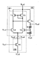
図1は、本発明の一態様の半導体装置の一例を示したブロック図である。半導体装置100は、配線REFLから参照電位が入力されることによって、配線OUTLから参照電位に応じた電位を出力するボルテージレギュレータである。半導体装置100は、回路101と、調整回路102と、回路103と、回路104と、保持回路SH1と、保持回路SH2と、を有する。<Configuration example>
FIG. 1 is a block diagram illustrating an example of a semiconductor device of one embodiment of the present invention. The
回路101は、端子TLa1乃至端子TLa5を有する。端子TLa1は、保持回路SH1に電気的に接続され、端子TLa2は、配線OUTLに電気的に接続され、端子TLa3は、配線VDDLに電気的に接続され、端子TLa5は、配線GNDLに電気的に接続されている。端子TLa4は、後述する回路103の端子TLc2に電気的に接続されている。 The
配線VDDLは、半導体装置100に高電源電位を与えるための配線であり、配線GNDLは、半導体装置100に低電源電位を与えるための配線である。なお、当該低電源電位としては、例えば、接地電位とすることができる。 The wiring VDDL is a wiring for applying a high power supply potential to the
回路101は、バイアス電流が端子TLa4に供給されることによって、端子TLa1に入力された電位に応じた出力電位を生成して、当該出力電位を端子TLa2から出力する機能を有する。そのため、回路101は、例えば、差動対を有する回路、バイアス電流が供給されることによって駆動する増幅回路などを有することができる。 The
回路103は、端子TLc1乃至端子TLc3を有する。端子TLc1は、後述する調整回路102の端子TLb2に電気的に接続され、端子TLc3は、配線GNDLに電気的に接続されている。 The
回路103は、回路101に入力するためのバイアス電流を生成する回路である。なお、当該バイアス電流の量は、端子TLc1に入力される電位に応じて決められる。 A
調整回路102は、端子TLb1乃至端子TLb4を有する。端子TLb1は、保持回路SH2に電気的に接続され、端子TLb3は、配線VDDLに電気的に接続され、端子TLb4は、配線GNDLに電気的に接続されている。 The
調整回路102は、端子TLb1及び端子TLb2の電位を変動させる機能を有する回路である。図1の回路構成より、端子TLb1及び端子TLb2の電位を変動させることによって、回路103の端子TLc1に入力される電位、及び保持回路SH2が有する容量素子C2の第1端子の電位も同時に変動させることができる。また、端子TLb1及び端子TLb2の電位を変動させることによって、回路103の端子TLc1に入力される電位を変動することができ、結果的に、回路103で生成されるバイアス電流の量を増減することができる。 The
回路104は、端子TLd1乃至端子TLd3を有する。端子TLd1は、保持回路SH2に電気的に接続され、端子TLd2は、配線VDD2Lに電気的に接続され、端子TLd3は、配線GNDLに電気的に接続されている。 The
配線VDD2Lは、回路104に所定の電位を与えるための配線である。なお、当該電位は、配線VDDLの高電源電位と等しくてもよい。そのため、端子TLd2は、配線VDD2Lでなく、配線VDDLに電気的に接続されていてもよい。 A wiring VDD2L is a wiring for applying a predetermined potential to the
回路104は、保持回路SH2の容量素子C2の第1端子、及び調整回路102の端子TLb1に所定の電位を入力するための回路として機能する。 The
保持回路SH1は、スイッチSW1と、容量素子C1と、を有する。スイッチSW1の第1端子は、配線REFLに電気的に接続され、スイッチSW1の第2端子は、容量素子C1の第1端子と、端子TLa1と、に電気的に接続されている。容量素子C1の第2端子は、配線GNDLに電気的に接続されている。 The holding circuit SH1 has a switch SW1 and a capacitive element C1. A first terminal of the switch SW1 is electrically connected to the wiring REFL, and a second terminal of the switch SW1 is electrically connected to the first terminal of the capacitor C1 and the terminal TLa1. A second terminal of the capacitive element C1 is electrically connected to the wiring GNDL.
また、スイッチSW1の制御端子は、配線SWLと電気的に接続されている。配線SWLは、スイッチSW1のオン状態とオフ状態との切り替えを行うための制御信号を送信する機能を有する配線である。 A control terminal of the switch SW1 is electrically connected to the wiring SWL. The wiring SWL is a wiring having a function of transmitting a control signal for switching the switch SW1 between an on state and an off state.
保持回路SH2は、スイッチSW2と、容量素子C2と、を有する。スイッチSW2の第1端子は、端子TLd1に電気的に接続され、スイッチSW2の第2端子は、容量素子C2の第1端子と、端子TLb1と、に電気的に接続されている。容量素子C2の第2端子は、配線GNDLに電気的に接続されている。 The holding circuit SH2 has a switch SW2 and a capacitive element C2. A first terminal of the switch SW2 is electrically connected to the terminal TLd1, and a second terminal of the switch SW2 is electrically connected to the first terminal of the capacitive element C2 and the terminal TLb1. A second terminal of the capacitive element C2 is electrically connected to the wiring GNDL.
また、スイッチSW2の制御端子は、配線SWLと電気的に接続されている。このため、スイッチSW1、及びスイッチSW2は、配線SWLから送られる制御信号に基づいて、互いに同期して、オン状態とオフ状態の切り替えを行う。具体的には、このような構成によって、スイッチSW1、及びスイッチSW2のそれぞれを、同時にオン状態、又はオフ状態にすることができる。 A control terminal of the switch SW2 is electrically connected to the wiring SWL. Therefore, the switch SW1 and the switch SW2 switch between the ON state and the OFF state in synchronization with each other based on the control signal sent from the wiring SWL. Specifically, with such a configuration, the switches SW1 and SW2 can be turned on or off at the same time.
本明細書に記載されているスイッチSW1及びスイッチSW2としては、例えば、トランジスタを適用することができ、また、スイッチSW1及びスイッチSW2が有する制御端子とは、当該トランジスタのゲートとすることができる。また、スイッチSW1及びスイッチSW2として、トランジスタを適用する場合、OSトランジスタであることが好ましい。特に、OSトランジスタは、チャネル形成領域にインジウム、元素M(元素Mは、アルミニウム、ガリウム、イットリウム、又はスズ)、亜鉛の少なくとも一を有する金属酸化物であることが好ましい。また、当該金属酸化物は、実施の形態3で詳述する。このようなOSトランジスタをスイッチSW1(スイッチSW2)に適用することで、トランジスタのオフ電流を非常に低くすることができる。そのため、容量素子C1の第1端子(容量素子C2の第1端子)に電位を保持する場合、スイッチSW1(スイッチSW2)をOSトランジスタとすることで、オフ電流による、容量素子C1(容量素子C2)に保持された電位の変動を防ぐことができる。 As the switches SW1 and SW2 described in this specification, for example, transistors can be applied, and the control terminals of the switches SW1 and SW2 can be the gates of the transistors. When transistors are used as the switches SW1 and SW2, they are preferably OS transistors. In particular, the OS transistor is preferably a metal oxide containing at least one of indium, element M (element M is aluminum, gallium, yttrium, or tin), and zinc in the channel formation region. Further, the metal oxide will be described in detail in the third embodiment. By applying such an OS transistor to the switch SW1 (switch SW2), the off-state current of the transistor can be significantly reduced. Therefore, when the potential is held at the first terminal of the capacitive element C1 (the first terminal of the capacitive element C2), the switch SW1 (switch SW2) is an OS transistor. ) can prevent fluctuations in the potential held in .
また、図1では、スイッチSW1の制御端子と、スイッチSW2の制御端子と、のそれぞれに配線SWLが電気的に接続されている構成を示しているが、本発明の一態様の半導体装置は、スイッチSW1の制御端子と、スイッチSW2の制御端子と、のそれぞれには、別々の配線が電気的に接続されている構成としてもよい。この構成により、スイッチSW1及びスイッチSW2は、互いに独立にオン状態とオフ状態の切り替えを行うことができる。 FIG. 1 illustrates a structure in which the wiring SWL is electrically connected to each of the control terminal of the switch SW1 and the control terminal of the switch SW2. Separate wires may be electrically connected to the control terminal of the switch SW1 and the control terminal of the switch SW2. With this configuration, the switches SW1 and SW2 can be switched between the ON state and the OFF state independently of each other.
保持回路SH1は、容量素子C1の第1端子の電位を保持することができる。具体的には、回路101内において、端子TLa1が、電源電位などの電位が与えられる配線に電気的に接続されていない場合において、スイッチSW1がオン状態のときに、容量素子C1の第1端子に配線REFLから入力される電位を書き込み、その後、スイッチSW1をオフ状態にすることによって、容量素子C1の第1端子及び回路101の端子TLa1のそれぞれの電位を保持することができる。同様に、保持回路SH2も、調整回路102内において端子TLb1と端子TLb2との間、及び、回路103内において端子TLc1、が電源電位などの電位が与えられる配線に電気的に接続されていない場合において、スイッチSW2がオン状態のときに、容量素子C2の第1端子に回路104の端子TLd1から入力される電位を書き込み、その後、スイッチSW2をオフ状態にすることによって、容量素子C2の第1端子の電位を保持することができる。 The holding circuit SH1 can hold the potential of the first terminal of the capacitive element C1. Specifically, in the
<<回路101、回路103>>
次に、回路101及び回路103の回路構成について説明する。図2は、回路101及び回路103の回路構成の例を示した図である。<<
Next, circuit configurations of the
図2に示す回路101は、オペアンプOP1を構成する一部の回路素子と、トランジスタTr1と、抵抗素子R1と、抵抗素子R2と、を有する。なお、トランジスタTr1は、pチャネル型トランジスタとする。また、オペアンプOP1はトランジスタTr2乃至トランジスタTr6を有している。なお、トランジスタTr2及びトランジスタTr3は、pチャネル型トランジスタであり、トランジスタTr4乃至トランジスタTr6は、nチャネル型トランジスタである。また、図2に示す回路103は、トランジスタTr6を有する。つまり、図2に示す回路101及び回路103の回路構成の例では、オペアンプOP1は、回路101の一部の回路素子と回路103とによって構成されている。また、この場合、オペアンプOP1は、バイアス電流を生成する機能と、当該バイアス電流によって差動対(トランジスタTr4とトランジスタTr5のそれぞれのゲート)に入力される電位に応じて出力電位を生成する機能と、を有する増幅回路として機能する。 The
トランジスタTr2の第1端子は、端子TLa3に電気的に接続され、トランジスタTr2の第2端子は、トランジスタTr1のゲートと、トランジスタTr4の第1端子と、に電気的に接続され、トランジスタTr2のゲートは、トランジスタTr3のゲートと、トランジスタTr3の第2端子と、に電気的に接続されている。トランジスタTr3の第1端子は、端子TLa3に電気的に接続され、トランジスタTr3の第2端子は、トランジスタTr5の第1端子に電気的に接続されている。 The first terminal of the transistor Tr2 is electrically connected to the terminal TLa3, the second terminal of the transistor Tr2 is electrically connected to the gate of the transistor Tr1 and the first terminal of the transistor Tr4, and the gate of the transistor Tr2. is electrically connected to the gate of the transistor Tr3 and the second terminal of the transistor Tr3. A first terminal of the transistor Tr3 is electrically connected to the terminal TLa3, and a second terminal of the transistor Tr3 is electrically connected to a first terminal of the transistor Tr5.
トランジスタTr4の第2端子は、端子TLa4に電気的に接続され、トランジスタTr4のゲートは、端子TLa1に電気的に接続されている。トランジスタTr5の第2端子は、端子TLa4に電気的に接続され、トランジスタTr5のゲートは、抵抗素子R1の第1端子と、抵抗素子R2の第1端子と、に電気的に接続されている。トランジスタTr6の第1端子は、端子TLc2に電気的に接続され、トランジスタTr6の第2端子は、端子TLc3に電気的に接続され、トランジスタTr6のゲートは、端子TLc1に電気的に接続されている。 A second terminal of the transistor Tr4 is electrically connected to the terminal TLa4, and a gate of the transistor Tr4 is electrically connected to the terminal TLa1. A second terminal of the transistor Tr5 is electrically connected to the terminal TLa4, and a gate of the transistor Tr5 is electrically connected to the first terminal of the resistance element R1 and the first terminal of the resistance element R2. A first terminal of the transistor Tr6 is electrically connected to the terminal TLc2, a second terminal of the transistor Tr6 is electrically connected to the terminal TLc3, and a gate of the transistor Tr6 is electrically connected to the terminal TLc1. .
つまり、トランジスタTr4のゲートは、オペアンプOP1の反転入力端子に相当し、トランジスタTr5のゲートは、オペアンプOP1の非反転入力端子に相当し、トランジスタTr2の第1端子及びトランジスタTr3の第1端子は、オペアンプOP1の高電源電位入力端子に相当し、トランジスタTr6の第2端子は、オペアンプOP1の低電源電位入力端子に相当する。 That is, the gate of the transistor Tr4 corresponds to the inverting input terminal of the operational amplifier OP1, the gate of the transistor Tr5 corresponds to the non-inverting input terminal of the operational amplifier OP1, and the first terminal of the transistor Tr2 and the first terminal of the transistor Tr3 are It corresponds to the high power supply potential input terminal of the operational amplifier OP1, and the second terminal of the transistor Tr6 corresponds to the low power supply potential input terminal of the operational amplifier OP1.
トランジスタTr1の第1端子は、端子TLa3に電気的に接続されている。端子TLa2は、トランジスタTr1の第2端子と、抵抗素子R1の第2端子と、に電気的に接続されている。端子TLa5は、抵抗素子R2の第2端子に電気的に接続されている。 A first terminal of the transistor Tr1 is electrically connected to the terminal TLa3. The terminal TLa2 is electrically connected to the second terminal of the transistor Tr1 and the second terminal of the resistance element R1. The terminal TLa5 is electrically connected to the second terminal of the resistive element R2.
抵抗素子R1、及び抵抗素子R2は、トランジスタTr5に印加するフィードバック電位を生成する役割を有している。そのため、抵抗素子R1及び/又は抵抗素子R2としては、代わりにトランジスタ、ダイオードなどの回路素子を適用することができる。 The resistive element R1 and the resistive element R2 have a role of generating a feedback potential to be applied to the transistor Tr5. Therefore, circuit elements such as transistors and diodes can be applied instead of the resistance element R1 and/or the resistance element R2.
回路101及び回路103を図2に示す回路構成にすることによって、オペアンプOP1の反転入力端子に配線REFLからの参照電位が入力されることで、参照電位に応じた電圧を回路101で生成して、端子TLa2から出力することができる。 By configuring the
なお、図2に示すオペアンプOP1において、高電源電位を与える端子TLa3とトランジスタTr2とトランジスタTr3と、によってカレントミラー回路が構成されており、トランジスタTr4及びトランジスタTr5によって、差動回路が構成されている。したがって、トランジスタTr2及びトランジスタTr3のそれぞれの構造、サイズは互いに同等であることが好ましく、トランジスタTr4及びトランジスタTr5のそれぞれの構造、サイズは互いに同等であることが好ましい。 In the operational amplifier OP1 shown in FIG. 2, the terminal TLa3, which supplies a high power supply potential, and the transistors Tr2 and Tr3 form a current mirror circuit, and the transistors Tr4 and Tr5 form a differential circuit. . Therefore, the structures and sizes of the transistors Tr2 and Tr3 are preferably the same, and the structures and the sizes of the transistors Tr4 and Tr5 are preferably the same.
次に、回路101及び回路103の具体的な動作について説明する。 Next, specific operations of the
高電源電位を与える端子TLa3と、トランジスタTr2と、トランジスタTr3と、によって、カレントミラー回路が構成されているため、トランジスタTr2及びトランジスタTr3のそれぞれのソース‐ドレイン間には、トランジスタTr3の第2端子の電位に応じた電流が流れる。 Since a current mirror circuit is configured by the terminal TLa3, which supplies a high power supply potential, the transistor Tr2, and the transistor Tr3, the second terminal of the transistor Tr3 is connected between the source and the drain of each of the transistors Tr2 and Tr3. A current flows according to the potential of
トランジスタTr3の第2端子の電位は、トランジスタTr5のゲートの電位に応じて決まる。具体的には、トランジスタTr5のゲートの電位と、端子TLa4から与えられる電位と、に応じて、トランジスタTr5のソース‐ドレイン間に電流が流れるため、トランジスタTr3の第2端子の電位は当該電流に応じた電位となる。 The potential of the second terminal of the transistor Tr3 is determined according to the potential of the gate of the transistor Tr5. Specifically, a current flows between the source and the drain of the transistor Tr5 in accordance with the potential of the gate of the transistor Tr5 and the potential applied from the terminal TLa4. It becomes the corresponding electric potential.
ここで、トランジスタTr4のゲートに(つまり、端子TLa1に)参照電位が入力されたとき、トランジスタTr4のソース‐ドレイン間に流れる電流は、参照電位と、端子TLa4から与えられる電位と、に応じて決まる。 Here, when the reference potential is input to the gate of the transistor Tr4 (that is, to the terminal TLa1), the current flowing between the source and the drain of the transistor Tr4 depends on the reference potential and the potential applied from the terminal TLa4. Determined.
このとき、参照電位よりもトランジスタTr5のゲートの電位が高い場合、トランジスタTr4のソース‐ドレイン電流よりもトランジスタTr5のソース‐ドレイン電流が大きくなるため、トランジスタTr2の第2端子(トランジスタTr1のゲート)の電位は高くなる。トランジスタTr1の第1端子は、高電源電位を与える端子TLa3と電気的に接続されているため、トランジスタTr1のゲートの電位が高くなると、トランジスタTr1のソース‐ドレイン電流が小さくなり、且つトランジスタTr1の第2端子は、抵抗素子R1と抵抗素子R2とを介して、低電源電位を与える端子TLa5と電気的に接続されているため、トランジスタTr1の第2端子の電位は低くなる。これにより、トランジスタTr5のゲートの電位も低くなるため、トランジスタTr5のソース‐ドレイン電流は小さくなる。最終的には、トランジスタTr5のゲートの電位は、トランジスタTr5のソース‐ドレイン電流がトランジスタTr4のソース‐ドレイン電流とほぼ等しくなるような電位に収束する。つまり、トランジスタTr5のゲートの電位は、参照電位とほぼ等しくなる。 At this time, when the potential of the gate of the transistor Tr5 is higher than the reference potential, the source-drain current of the transistor Tr5 becomes larger than the source-drain current of the transistor Tr4. becomes higher. Since the first terminal of the transistor Tr1 is electrically connected to the terminal TLa3 that supplies a high power supply potential, when the potential of the gate of the transistor Tr1 increases, the source-drain current of the transistor Tr1 decreases and the current of the transistor Tr1 increases. Since the second terminal is electrically connected through the resistance elements R1 and R2 to the terminal TLa5 that supplies the low power supply potential, the potential of the second terminal of the transistor Tr1 becomes low. As a result, the potential of the gate of the transistor Tr5 also decreases, so the source-drain current of the transistor Tr5 decreases. Eventually, the potential of the gate of transistor Tr5 converges to a potential such that the source-drain current of transistor Tr5 is approximately equal to the source-drain current of transistor Tr4. That is, the potential of the gate of transistor Tr5 becomes substantially equal to the reference potential.
また、参照電位よりもトランジスタTr5のゲートの電位が低い場合、トランジスタTr5のソース‐ドレイン電流よりもトランジスタTr4のソース‐ドレイン電流が大きくなるため、トランジスタTr2の第2端子(トランジスタTr1のゲート)の電位は低くなる。トランジスタTr1の第1端子は、高電源電位を与える端子TLa3と電気的に接続されているため、トランジスタTr1のゲートの電位が低くなると、トランジスタTr1のソース‐ドレイン電流が大きくなるため、トランジスタTr1の第2端子の電位は高くなる。これにより、トランジスタTr5のゲートの電位も高くなるため、トランジスタTr5のソース‐ドレイン電流は大きくなる。最終的には、トランジスタTr5のゲートの電位は、トランジスタTr5のソース‐ドレイン電流がトランジスタTr4のソース‐ドレイン電流とほぼ等しくなるような電位に収束する。つまり、トランジスタTr5のゲートの電位は、参照電位とほぼ等しくなる。 Further, when the potential of the gate of the transistor Tr5 is lower than the reference potential, the source-drain current of the transistor Tr4 becomes larger than the source-drain current of the transistor Tr5. potential becomes lower. Since the first terminal of the transistor Tr1 is electrically connected to the terminal TLa3 that supplies a high power supply potential, when the potential of the gate of the transistor Tr1 decreases, the source-drain current of the transistor Tr1 increases. The potential of the second terminal becomes higher. As a result, the potential of the gate of the transistor Tr5 also increases, so that the source-drain current of the transistor Tr5 increases. Eventually, the potential of the gate of transistor Tr5 converges to a potential such that the source-drain current of transistor Tr5 is approximately equal to the source-drain current of transistor Tr4. That is, the potential of the gate of transistor Tr5 becomes substantially equal to the reference potential.
ここで、端子TLa2から出力される電位は、端子TLa1に入力される参照電位に加え、抵抗素子R1及び抵抗素子R2のそれぞれの抵抗値によって決められる。つまり、抵抗素子R1及び抵抗素子R2のそれぞれの抵抗値を定めることによって、端子TLa2から出力される電位を任意に設定することができる。なお、端子TLa1に入力された参照電位とほぼ等しい電位を端子TLa2から出力したい場合は、抵抗素子R1を限りなく0とすればよい。 Here, the potential output from the terminal TLa2 is determined by the resistance values of the resistance elements R1 and R2 in addition to the reference potential input to the terminal TLa1. In other words, the potential output from the terminal TLa2 can be arbitrarily set by determining the resistance values of the resistance elements R1 and R2. If it is desired to output from the terminal TLa2 a potential substantially equal to the reference potential input to the terminal TLa1, the resistance element R1 should be set to 0 as much as possible.
<<調整回路102>>
次に、調整回路102の回路構成について説明する。図3(A)は、調整回路102の回路構成の例を示した図である。<<
Next, the circuit configuration of the
図3(A)に示す調整回路102は、回路102aと、容量素子C3と、を有する。 The
容量素子C3の第1端子は、端子TLb1と、端子TLb2と、に電気的に接続されている。容量素子C3の第2端子は、回路102aの出力端子に電気的に接続されている。回路102aの入力端子は、配線ADJLに電気的に接続され、回路102aの高電源電位入力端子は、端子TLb3に電気的に接続され、回路102aの低電源電位入力端子は、端子TLb4に電気的に接続されている。 A first terminal of the capacitive element C3 is electrically connected to the terminal TLb1 and the terminal TLb2. A second terminal of the capacitive element C3 is electrically connected to the output terminal of the
配線ADJLは、回路102aに対して入力電位を与える配線であり、回路102aは、容量素子C3の第2端子に入力電位に応じた電位を印加する機能を有する回路である。つまり、端子TLb1及び端子TLb2に電気的に接続されている配線が電気的に浮遊状態であるとき、調整回路102は、容量素子C3の第2端子に電位を印加することで、容量素子C3による容量結合によって、端子TLb1及び端子TLb2と電気的に接続されている配線の電位を変動することができる回路構成となっている。なお、調整回路102は、回路102aを省略した構成、つまり、配線ADJLと容量素子C3の第2端子とが直接電気的に接続されている構成としてもよい(図示しない。)。 The wiring ADJL is a wiring that supplies an input potential to the
また、調整回路102は、図1に示す半導体装置100の保持回路SH2を含んだ構成としてもよい。そのような回路構成を図3(B)に示す。図3(B)の調整回路102は、図1に示す半導体装置100の調整回路102と保持回路SH2とを一括りとした回路であり、図3(A)の調整回路102の容量素子C3による容量結合によって容量素子C3の第1端子の電位を変動させる機能に加えて、容量素子C2の第1端子(容量素子C3の第1端子)の電位を保持する機能を有する。 Further, the
回路102aとしては、例えば、図3(C)に示すとおり、バッファ回路BUFを適用することができる。この場合、バッファ回路BUFの入力端子は、回路102aの入力端子に相当し、バッファ回路BUFの出力端子は、回路102aの出力端子に相当する。バッファ回路BUFの高電源入力端子は、端子TLb3に電気的に接続され、バッファ回路BUFの低電源入力端子は、端子TLb4に電気的に接続されている。なお、バッファ回路BUFとしては、デジタルバッファ回路、アナログバッファ回路などを適用することができる。 As the
また、回路102aは、複数の電位のうちの一を容量素子C3の第2端子に印加する構成としてもよい。そのような回路構成を図3(D)に示す。図3(D)に示す調整回路102では、回路102aとして、マルチプレクサMUXを適用している。マルチプレクサは、n個(nは2以上の整数とする。)の入力端子を有し、n個の入力端子のそれぞれは、配線ADJL[1]乃至配線ADJL[n]と電気的に接続されている。なお、図3(D)の調整回路102の場合、端子TLb3、端子TLb4を設けなくてもよい。 Alternatively, the
配線ADJL[1]乃至配線ADJL[n]のそれぞれは、互いに異なる電位を与える配線とする。配線CTLは、マルチプレクサMUXに電気的に接続されており、マルチプレクサMUXに対して選択信号を送信する配線である。マルチプレクサMUXは、当該選択信号を受け取ることにより、当該選択信号に含まれる内容に応じてマルチプレクサMUXのn個の入力端子のいずれか一を選択して、選択された入力端子と出力端子とを電気的に接続する機能を有する。このような構成にすることにより、マルチプレクサMUXは、配線ADJL[1]乃至配線ADJL[n]のいずれか一を選択して、選択された配線が与える電位を容量素子C3の第2端子に印加することができる。なお、図3(D)において、配線CTLは複数の配線として図示しているが、nが2である場合、1本の配線とすることができる。 The wirings ADJL[1] to ADJL[n] are wirings to which different potentials are applied. The wiring CTL is electrically connected to the multiplexer MUX and is a wiring that transmits a selection signal to the multiplexer MUX. Upon receiving the selection signal, the multiplexer MUX selects one of the n input terminals of the multiplexer MUX according to the contents included in the selection signal, and electrically connects the selected input terminal and the output terminal. It has the function of connecting With such a configuration, the multiplexer MUX selects any one of the wirings ADJL[1] to ADJL[n] and applies the potential given by the selected wiring to the second terminal of the capacitive element C3. can do. Note that although the wiring CTL is illustrated as a plurality of wirings in FIG. 3D, when n is 2, it can be one wiring.
また、マルチプレクサMUXの出力端子と、容量素子C3の第2端子と、の間にアナログバッファ回路ABUFを設けた回路としてもよい。この場合、図3(E)に示すとおり、当該回路は、マルチプレクサMUXの出力端子とアナログバッファ回路ABUFの入力端子とを電気的に接続し、アナログバッファ回路ABUFの出力端子と容量素子C3の第2端子とを電気的に接続した構成とすればよい。また、図3(C)と図3(D)とのそれぞれの調整回路102を組み合わせてもよい。この場合、図3(F)に示すとおり、端子TLb1と端子TLb2間の配線に対して、容量素子C3の第1端子と容量素子C4の第1端子を並列に電気的に接続し、容量素子C3の第2端子にマルチプレクサMUXの出力端子を電気的に接続し、容量素子C4の第2端子にバッファ回路BUFの出力端子を電気的に接続した構成としてもよい。 Alternatively, a circuit may be provided in which an analog buffer circuit ABUF is provided between the output terminal of the multiplexer MUX and the second terminal of the capacitive element C3. In this case, as shown in FIG. 3E, the circuit electrically connects the output terminal of the multiplexer MUX and the input terminal of the analog buffer circuit ABUF, and A configuration in which the two terminals are electrically connected may be used. Also, the
また、回路102aは、回路101の端子TLa2から出力される電位に応じて、容量素子C3の第2端子に与える電位を変化させる構成としてもよい。そのような回路構成を図3(G)に示す。図3(G)に示す調整回路102では、回路102aとして、コンパレータCMP1を適用している。コンパレータCMP1の非反転入力端子は、配線REGLに電気的に接続され、コンパレータCMP1の反転入力端子は、配線CRFLに電気的に接続され、コンパレータCMP1の出力端子は、容量素子C3の第2端子に接続されている。なお、コンパレータCMP1の電源電位入力端子には、端子TLb3及び/又は端子TLb4が電気的に接続されていてもよいし、端子TLb3及びTLb4とは別の電源電位を与える端子に電気的に接続されていてもよい。 Alternatively, the
配線REGLには、回路101の端子TLa2から出力される電位が入力される。また、配線CRFLは、コンパレータCMP1における基準電位が入力されている。 A potential output from the terminal TLa2 of the
図3(G)に示す調整回路102において、配線REGLの電位が配線CRFLの電位よりも低いとき、つまり、回路101の端子TLa2から出力される電位が、当該基準電位よりも低いとき、コンパレータCMP1の出力端子は、高レベル電位を出力する。このとき、容量素子C3の第2端子には高レベル電位が与えられる。端子TLb1及び端子TLb2に電気的に接続されている配線が電気的に浮遊状態であるとき、当該配線の電位は容量素子C3の容量結合によって高くなる。 In the
また、配線REGLの電位が配線CRFLの基準電位よりも高いとき、つまり、回路101の端子TLa2から出力される電位が、当該基準電位よりも高いとき、コンパレータCMP1の出力端子は、低レベル電位を出力する。端子TLb1及び端子TLb2に電気的に接続されている配線が電気的に浮遊状態であるとき、当該配線の電位は容量素子C3の容量結合によって低くなる。 Further, when the potential of the wiring REGL is higher than the reference potential of the wiring CRFL, that is, when the potential output from the terminal TLa2 of the
なお、図3(G)に示す調整回路102を用いた場合の半導体装置100の動作については、動作例にて詳述する。 Note that the operation of the
ところで、コンパレータCMP1は、代わりとしてクロックトコンパレータCMP2を適用することができる。図3(H)の調整回路102は、図3(G)の調整回路102のコンパレータCMP1としてクロックトコンパレータCMP2を適用した回路構成となっており、クロックトコンパレータCMP2のクロック信号入力端子には、クロック信号を与える配線CLKLが電気的に接続されている。 By the way, the comparator CMP1 can be replaced by a clocked comparator CMP2. The
また、調整回路102は、複数の回路102aと、複数の容量素子C3と、を有する回路構成としてもよい。具体的には、調整回路102は、図4(A)に示す回路構成としてもよい。図4(A)に示す調整回路102は、複数の回路102aとして回路102a[1]乃至回路102a[n]と、複数の容量素子C3として容量素子C3[1]乃至容量素子C3[n]と、を有する。 Further, the
容量素子C3[j](jは1以上n以下の整数とする。)の第1端子は、端子TLb1と、端子TLb2と、に電気的に接続されている。容量素子C3[j]の第2端子は、回路102a[j]の出力端子に電気的に接続されている。回路102a[j]の入力端子は、配線ADJL[j]に電気的に接続され、回路102a[j]の高電源電位入力端子は、端子TLb3に電気的に接続され、回路102a[j]の低電源電位入力端子は、端子TLb4に電気的に接続されている。 A first terminal of the capacitor C3[j] (j is an integer greater than or equal to 1 and less than or equal to n) is electrically connected to the terminal TLb1 and the terminal TLb2. A second terminal of the capacitive element C3[j] is electrically connected to the output terminal of the
このような構成にすることにより、回路102a[1]乃至回路102a[n]と容量素子C3[1]乃至容量素子C3[n]と、によって、端子TLb1と端子TLb2と電気的に接続されている配線の電位を変動させることができる。また、回路102a[1]乃至回路102a[n]のうち駆動を行う回路を1つ又は複数選択することによって、端子TLb1と端子TLb2と電気的に接続されている配線の電位を様々に変動させることができる。 With such a structure, the terminals TLb1 and TLb2 are electrically connected by the
例えば、容量素子C3[1]乃至容量素子C3[n]の静電容量の値を全てほぼ等しくし、且つ配線ADJL[j]が与える電位を2j-1×Vany(Vanyは任意の電位とする。)とすることによって、回路102a[1]乃至回路102a[n]のうち駆動を行う回路を1つ又は複数選択することで、容量素子C3[1]乃至容量素子C3[n]の第2端子に合計k×Vany(kは0以上2n-1以下の整数である。)の電位を与えることができる。つまり、この合計の電位に応じて、端子TLb1と端子TLb2と電気的に接続されている配線の電位を変動させることができる。For example, the capacitance values of the capacitive elements C3[1] to C3[n] are all made substantially equal, and the potential applied to the wiring ADJL[j] is set to 2 j−1 ×V any (V any is an arbitrary By selecting one or more of the
また、例えば、配線ADJL[1]乃至配線ADJL[n]のそれぞれが与える電位をVanyとし、且つ容量素子C3[1]乃至容量素子C3[n]のそれぞれの静電容量を異なる値とすることによって、回路102a[1]乃至回路102a[n]のうち駆動を行う回路を1つ又は複数選択することで、端子TLb1と端子TLb2と電気的に接続されている配線の電位を様々に変動させることができる。Further, for example, the potential applied by each of the wirings ADJL[1] to ADJL[n] is Vany , and the capacitances of the capacitors C3[1] to C3[n] are different values. Therefore, by selecting one or more of the
なお、図4(A)に示す調整回路102の構成では、端子TLb1、端子TLb2、端子TLb3、端子TLb4、配線ADJL[1]、配線ADJL[n]、容量素子C3[1]、容量素子C3[n]、回路102a[1]、回路102a[n]のみ図示しており、それ以外の回路、素子、配線などを省略している。 Note that in the configuration of the
また、図4(A)に示す調整回路102において、回路102a[1]乃至回路102a[n]の一部を選択して、選択された回路への電力の供給を停止する構成としてもよい。そのような回路構成を図4(B)に示す。図4(B)に示す調整回路102は、高電源電位を与える端子TLb3と回路102a[1]乃至回路102a[n]のそれぞれの高電源電位入力端子との間にスイッチSWa[1]乃至スイッチSWa[n]が設けられ、低電源電位を与える端子TLb4と回路102a[1]乃至回路102a[n]のそれぞれの低電源電位入力端子との間にスイッチSWb[1]乃至スイッチSWb[n]が設けられた構成となっている。なお、スイッチSWa[1]乃至スイッチSWa[n]のそれぞれには、配線SWBL[1]乃至配線SWBL[n]が電気的に接続され、スイッチSWb[1]乃至スイッチSWb[n]のそれぞれには、配線SWBL[1]乃至配線SWBL[n]が電気的に接続されている。また、スイッチSWa[j]、スイッチSWb[j]のオン状態、オフ状態の切り替えは配線SWBL[j]から送られる信号によって行われる。調整回路102をこのような構成にすることによって、配線SWBL[1]乃至配線SWBL[n]によって、回路102a[1]乃至回路102a[n]のうち所望の回路を選択して、該当する回路への電力の供給を停止することができる。これにより、回路102a[1]乃至回路102a[n]のうち必要な回路のみ駆動することができるため、調整回路102に必要な消費電力を削減することができる。 Further, in the
なお、図4(B)に示す調整回路102の構成では、端子TLb1、端子TLb2、端子TLb3、端子TLb4、配線ADJL[1]、配線ADJL[n]、配線SWBL[1]、配線SWBL[n]、容量素子C3[1]、容量素子C3[n]、スイッチSWa[1]、スイッチSWa[n]、スイッチSWb[1]、スイッチSWb[n]、回路102a[1]、回路102a[n]のみ図示しており、それ以外の回路、素子、配線などを省略している。 Note that in the configuration of the
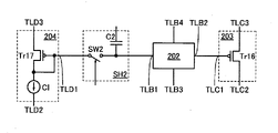
<<回路103、回路104>>
次に、回路103及び回路104の回路構成について説明する。図5は、回路103及び回路104の回路構成の例を示した図である。なお、回路103及び回路104の接続構成を説明するため、図5では、調整回路102及び保持回路SH2も図示している。<<
Next, circuit configurations of the
回路103は、図2の説明の通りトランジスタTr6を有し、回路104は、トランジスタTr7と、定電流源CIと、を有している。なお、トランジスタTr7は、nチャネル型トランジスタとする。 The
図2の説明のとおり、トランジスタTr6の第1端子は、端子TLc2に電気的に接続され、トランジスタTr6の第2端子は、端子TLc3に電気的に接続され、トランジスタTr6のゲートは、端子TLc1に電気的に接続されている。トランジスタTr7の第1端子は、定電流源CIの出力端子と、トランジスタTr7のゲートと、に電気的に接続され、トランジスタTr7の第2端子は、端子TLd3に電気的に接続され、トランジスタTr7のゲートは、端子TLd1に電気的に接続されている。定電流源CIの入力端子は、端子TLd2に電気的に接続されている。 As described with reference to FIG. 2, the first terminal of the transistor Tr6 is electrically connected to the terminal TLc2, the second terminal of the transistor Tr6 is electrically connected to the terminal TLc3, and the gate of the transistor Tr6 is connected to the terminal TLc1. electrically connected. A first terminal of the transistor Tr7 is electrically connected to the output terminal of the constant current source CI and the gate of the transistor Tr7, and a second terminal of the transistor Tr7 is electrically connected to the terminal TLd3. The gate is electrically connected to terminal TLd1. The input terminal of constant current source CI is electrically connected to terminal TLd2.
ところで、図3(A)乃至(H)、図4(A)(B)に示す回路構成より、調整回路102の端子TLb1と端子TLb2との間は、電気的に接続されている。つまり、保持回路SH2のスイッチSW2がオン状態となっているとき、回路103の端子TLc1と、回路104の端子TLd1と、の間が導通状態になるため、回路103と回路104とによって、カレントミラー回路が構成される。なお、トランジスタTr6とトランジスタTr7の構造、サイズは互いに同等であってもよいし、或いは互いに異なっていてもよい。 By the way, the terminals TLb1 and TLb2 of the
また、上述したトランジスタTr1乃至トランジスタTr7としては、例えば、チャネル形成領域にシリコンを有するトランジスタ(以後、Siトランジスタと記載する。)とすることができる。シリコンとしては、例えば、水素化アモルファスシリコン、微結晶シリコン、多結晶シリコン、単結晶シリコン等を用いることができる。また、トランジスタTr1乃至トランジスタTr7をSiトランジスタとする場合、半導体装置100は、トランジスタTr1乃至トランジスタTr7を単結晶シリコン基板上に形成する構成とするのが好ましい。また、当該構成については、実施の形態3で詳述する。 Further, as the transistors Tr1 to Tr7 described above, for example, a transistor including silicon in a channel formation region (hereinafter referred to as a Si transistor) can be used. As silicon, for example, hydrogenated amorphous silicon, microcrystalline silicon, polycrystalline silicon, monocrystalline silicon, or the like can be used. When the transistors Tr1 to Tr7 are Si transistors, the
<動作例>
次に、本発明の一態様の半導体装置の動作例について説明する。なお、本動作例では、図6に示す半導体装置100Aの動作について説明する。<Operation example>
Next, an operation example of the semiconductor device of one embodiment of the present invention is described. In this operation example, the operation of the
図6に示す半導体装置100Aでは、回路101を図2(B)に示す回路構成とし、回路103及び回路104を図5に示す回路構成としている。 In the
また、半導体装置100Aの調整回路102は、図3(B)に示す調整回路102と図4(A)に示す調整回路102とを組み合わせた回路構成としている。具体的には、図4(A)に示す回路102a[1]乃至回路102a[n]として、バッファ回路BUF[1]乃至バッファ回路BUF[n]を適用している。 The
また、半導体装置100Aの保持回路SH1は、スイッチSW1としてトランジスタOTr1を適用している。なお、トランジスタOTr1の第1端子は、スイッチSW1の第1端子に相当し、トランジスタOTr1の第2端子は、スイッチSW1の第2端子に相当し、トランジスタOTr1のゲートは、スイッチSW1の制御端子に相当するものとする。トランジスタOTr1は、バックゲートを有するトランジスタであり、トランジスタOTr1のバックゲートは、トランジスタOTr1のゲートと電気的に接続されている。このような接続構成にすることによって、トランジスタOTr1は、オン電流を大きくすることができる。また、保持回路SH1を、トランジスタOTr1のバックゲートがトランジスタOTr1のゲートでなく別の配線に電気的に接続されている構成とし、当該配線に所定の電位を与えることで、トランジスタOTr1のしきい値電圧を変動させることができる。なお、トランジスタOTr1は、バックゲートを有さないトランジスタとしてもよい。また、トランジスタOTr1は、容量素子C1の第1端子に書き込む電位を長時間保持することが好ましいため、オフ電流が極めて小さい特性を有するOSトランジスタを用いるのが好ましい。 The holding circuit SH1 of the
本動作例において、トランジスタOTr1の第2端子と容量素子C1の電気的接続点をノードND1と呼称する。 In this operation example, the electrical connection point between the second terminal of the transistor OTr1 and the capacitive element C1 is referred to as a node ND1.
また、半導体装置100Aの保持回路SH2は、スイッチSW2としてトランジスタOTr2を適用している。なお、トランジスタOTr2の第1端子は、スイッチSW2の第1端子に相当し、トランジスタOTr2の第2端子は、スイッチSW2の第2端子に相当し、トランジスタOTr2のゲートは、スイッチSW2の制御端子に相当するものとする。トランジスタOTr2は、トランジスタOTr1と同様に、バックゲートを有するトランジスタであり、トランジスタOTr2のバックゲートは、トランジスタOTr2のゲートと電気的に接続されている。なお、半導体装置100Aの保持回路SH2の構成は、半導体装置100Aの保持回路SH1の構成と等しいため、トランジスタOTr2の説明は、前述のトランジスタOTr1の説明の記載を参酌する。 The holding circuit SH2 of the
本動作例において、トランジスタOTr2の第2端子と容量素子C2の電気的接続点をノードND2と呼称する。 In this operation example, the electrical connection point between the second terminal of the transistor OTr2 and the capacitive element C2 is referred to as a node ND2.
また、図1では、保持回路SH1及び保持回路SH2は、配線SWLに電気的に接続された構成が図示されているが、図6では、保持回路SH1は配線SW1Lに電気的に接続され、保持回路SH2は配線SW2Lに電気的に接続された構成が図示されている。つまり、保持回路SH1及び保持回路SH2は、トランジスタOTr1のオン状態、オフ状態の切り替えは、配線SW1Lから送られる信号によって行われ、トランジスタOTr2のオン状態、オフ状態の切り替えは、配線SW2Lから送られる信号によって行われる構成としている。換言すると、トランジスタOTr1及びトランジスタOTr2のそれぞれは、互いに独立にオン状態、オフ状態の切り替えを行うことができる。 1 illustrates a configuration in which the holding circuit SH1 and the holding circuit SH2 are electrically connected to the wiring SWL, the holding circuit SH1 is electrically connected to the wiring SW1L in FIG. A configuration in which the circuit SH2 is electrically connected to the wiring SW2L is illustrated. That is, in the holding circuits SH1 and SH2, switching between the on state and the off state of the transistor OTr1 is performed by a signal sent from the wiring SW1L, and switching between the on state and the off state of the transistor OTr2 is performed by the wiring SW2L. It is configured to be performed by a signal. In other words, each of the transistors OTr1 and OTr2 can be switched between the ON state and the OFF state independently of each other.
なお、本動作例において、トランジスタOTr1及びトランジスタOTr2は、特に断りの無い場合は、オン状態の場合は最終的に線形領域で動作するものとする。つまり、トランジスタOTr1及びトランジスタOTr2のゲート電圧、ソース電圧、及びドレイン電圧は、線形領域で動作する範囲の電圧として適切にバイアスされているのものとする。 In this operation example, unless otherwise specified, the transistor OTr1 and the transistor OTr2 are assumed to finally operate in the linear region when in the ON state. That is, it is assumed that the gate voltage, source voltage, and drain voltage of the transistors OTr1 and OTr2 are appropriately biased as voltages within the range of operation in the linear region.
また、トランジスタTr1乃至トランジスタTr7は、特に断りの無い場合は、飽和領域で動作するものとする。つまり、トランジスタTr1乃至トランジスタTr7のゲート電圧、ソース電圧、及びドレイン電圧は、飽和領域で動作する範囲の電圧として適切にバイアスされているものとする。 In addition, the transistors Tr1 to Tr7 are assumed to operate in the saturation region unless otherwise specified. In other words, it is assumed that the gate voltage, source voltage, and drain voltage of the transistors Tr1 to Tr7 are appropriately biased as voltages within the range of operation in the saturation region.
次に、半導体装置100Aの具体的な動作例について説明する。図7(A)(B)は、半導体装置100Aの動作例を示すタイミングチャートである。図7(A)のタイミングチャートは、調整回路102が動作しない場合における、時刻T01から時刻T05までの間とその近傍での、配線SW1L、配線SW2L、配線REFL、配線OUTL、ノードND1、ノードND2、配線ADJL[1]の電位の変化を示している。加えて、図7(B)のタイミングチャートは、調整回路102が動作する場合における、時刻T11から時刻T16までの間とその近傍での、配線SW1L、配線SW2L、配線REFL、配線OUTL、ノードND1、ノードND2、配線ADJL[1]の電位の変化を示している。なお、図7(A)(B)のタイミングチャートに示す、「high」は高レベル電位を指し、「low」は低レベル電位を指し、VGNDは接地電位を指す。なお、本明細書などにおいて、「低レベル電位」、「高レベル電位」という用語は、特定の電位を意味するものではなく、配線が異なれば、具体的な電位も異なる場合がある。そのため、例えば、配線SW1Lが与える高レベル電位は、配線SW2Lが与える高レベル電位と異なる電位であってもよい。また、例えば、配線SW1Lが与える低レベル電位は、配線SW2Lが与える低レベル電位と異なる電位であってもよい。Next, a specific operation example of the
<<調整回路102を駆動しない場合>>
初めに、調整回路102を駆動しない場合(図7(A))の、半導体装置100Aの動作例について説明する。<<When adjusting
First, an operation example of the
なお、図7(A)のタイミングチャートでは、調整回路102を駆動しないため、時刻T01から時刻T05までの間とその近傍において、配線ADJL[1]乃至配線ADJL[n]には、VGNDが印加されている。Note that in the timing chart of FIG. 7A, since the
〔時刻T01より前〕
時刻T01より前において、配線SW1L及び配線SW2Lには、低レベル電位が印加されている。そのため、保持回路SH1に含まれるトランジスタOTr1のゲートに低レベル電位が印加されるため、トランジスタOTr1はオフ状態となる。加えて、保持回路SH2に含まれるトランジスタOTr2のゲートに低レベル電位が印加されるため、トランジスタOTr2もオフ状態となる。[Before time T01]
Before time T01, a low-level potential is applied to the wiring SW1L and the wiring SW2L. Therefore, since a low level potential is applied to the gate of the transistor OTr1 included in the holding circuit SH1, the transistor OTr1 is turned off. In addition, since a low level potential is applied to the gate of the transistor OTr2 included in the holding circuit SH2, the transistor OTr2 is also turned off.
また、配線REFLには、VGNDが印加されている。なお、配線REFLには、この段階において、VGNDでなく、参照電位、又は任意の電位が印加されていてもよい。Further, V GND is applied to the wiring REFL. Note that a reference potential or an arbitrary potential may be applied to the wiring REFL at this stage instead of VGND .
時刻T01より前において、ノードND1、及びノードND2の電位は、それぞれVG NDとする。なお、ノードND1、及びノードND2のそれぞれは、VGND以外の電位であってもよい。Before time T01, the potentials of the nodes ND1 and ND2 are V GND. Note that each of the node ND1 and the node ND2 may have a potential other than VGND .
なお、時刻T01より前において、配線OUTLの電位は不定であるが、図7では、V GNDとしている。 Although the potential of the wiring OUTL is indefinite before time T01, in FIG. GNDand
〔時刻T01から時刻T02までの間〕
時刻T01から時刻T02までの間において、配線SW2Lには、高レベル電位が印加される。そのため、保持回路SH2に含まれるトランジスタOTr2のゲートに高レベル電位が印加されるため、トランジスタOTr2はオン状態となる。[Between time T01 and time T02]
A high-level potential is applied to the wiring SW2L from time T01 to time T02. Therefore, since a high level potential is applied to the gate of the transistor OTr2 included in the holding circuit SH2, the transistor OTr2 is turned on.
トランジスタOTr2がオン状態になると、回路103の端子TLc1と、回路104の端子TLd1と、の間が導通状態になるため、回路103と回路104とによるカレントミラー回路が動作する。これにより、トランジスタTr6とトランジスタTr7とのそれぞれに、ほぼ等しいソース‐ドレイン電流が流れる。また、このソース‐ドレイン電流の大きさは、定電流源CIの仕様によって決まる。また、定電流源CIの仕様により、回路103の端子TLc1と回路104の端子TLd1との間の配線(ノードND2)の電位が決まり、当該電位は、保持回路SH2の容量素子C2の第1端子に書き込まれる。本動作例において、当該電位をVBSと記載する。When the transistor OTr2 is turned on, electrical continuity is established between the terminal TLc1 of the
回路103の端子TLc3と、回路104の端子TLd3と、のそれぞれが配線GNDLに電気的に接続されているため、トランジスタTr6に発生するソース‐ドレイン電流は、回路103の端子TLc2から端子TLc3への方向に流れる。つまり、回路103と回路104とによるカレントミラー回路が動作することによって、回路101の端子TLa4から電流の排出が行われる。 Since the terminal TLc3 of the
ノードND2の電位がVBSに達した後において、配線SW2Lには、低レベル電位が印加される。そのため、保持回路SH2に含まれるトランジスタOTr2のゲートに低レベル電位が印加されるため、トランジスタOTr2はオフ状態となる。After the potential of the node ND2 reaches VBS, a low level potential is applied to the wiring SW2L. Therefore, since a low level potential is applied to the gate of the transistor OTr2 included in the holding circuit SH2, the transistor OTr2 is turned off.
このとき、ノードND2は電気的に浮遊状態となり、ノードND2の電位であるVBSは保持回路SH2に含まれている容量素子C2によって保持される。また、ここで、定電流源CIを停止した場合、トランジスタTr7のソース‐ドレイン間に電流は流れなくなるが、トランジスタTr6のゲート、つまりノードND2の電位のVBSは保持されているため、トランジスタTr6のソース‐ドレイン間には電流が流れる。つまり、定電流源CIを停止しても、トランジスタTr6のソース‐ドレイン間に電流を流すことができるため、定電流源CIを駆動するための消費電力を低減することができる。At this time, the node ND2 is in an electrically floating state, and the potential VBS of the node ND2 is held by the capacitive element C2 included in the holding circuit SH2. If the constant current source CI is stopped here, no current flows between the source and the drain of the transistor Tr7 , but the gate of the transistor Tr6, that is, the potential VBS of the node ND2 is held. current flows between the source and drain of That is, even if the constant current source CI is stopped, a current can flow between the source and the drain of the transistor Tr6, so that the power consumption for driving the constant current source CI can be reduced.
〔時刻T02から時刻T03までの間〕
時刻T02から時刻T03までの間において、半導体装置100Aには、配線REFLから参照電位としてVREFが与えられる。[Between time T02 and time T03]
From time T02 to time T03, the
なお、この時点では、トランジスタOTr1がオフ状態であるため、配線REFLからVREFが与えられることによる、ノードND1の電位の変動は起こらない。Note that since the transistor OTr1 is off at this point, the potential of the node ND1 does not fluctuate due to the application of VREF from the wiring REFL.
〔時刻T03から時刻T04までの間〕
時刻T03から時刻T04までの間において、配線SW1Lには、高レベル電位が印加される。そのため、保持回路SH1に含まれるトランジスタOTr1のゲートに高レベル電位が印加されるため、トランジスタOTr1はオン状態となる。[Between time T03 and time T04]
A high-level potential is applied to the wiring SW1L from time T03 to time T04. Therefore, since a high level potential is applied to the gate of the transistor OTr1 included in the holding circuit SH1, the transistor OTr1 is turned on.
トランジスタOTr1がオン状態になると、配線REFLとノードND1との間が電気的に接続されるため、ノードND1の電位はVREFとなる。また、このとき、ノードND1の電位VREFは、保持回路SH1の容量素子C1の第1端子に書き込まれる。When the transistor OTr1 is turned on, the wiring REFL and the node ND1 are electrically connected to each other, so that the potential of the node ND1 becomes VREF. At this time, the potential VREF of the node ND1 is written to the first terminal of the capacitor C1 of the holding circuit SH1.
ノードND1の電位がVREFに達した後において、配線SW1Lには、低レベル電位が印加される。そのため、保持回路SH1に含まれるトランジスタOTr1のゲートに低レベル電位が印加されるため、トランジスタOTr1はオフ状態となる。After the potential of the node ND1 reaches VREF, a low level potential is applied to the wiring SW1L . Therefore, since a low level potential is applied to the gate of the transistor OTr1 included in the holding circuit SH1, the transistor OTr1 is turned off.
このとき、ノードND1は電気的に浮遊状態となり、ノードND1の電位であるVRE Fは保持回路SH1に含まれている容量素子C1によって保持される。At this time, the node ND1 is in an electrically floating state, and the potential V REF of the node ND1 is held by the capacitive element C1 included in the holding circuit SH1.
また、回路101の端子TLa1には、VREFが入力される。本動作例では、抵抗素子R1の抵抗値が限りなく0に近い場合を考えるものとする。そのため、回路101は、端子TLa1に入力された電位とほぼ等しい電位を端子TLa2から出力するため、配線OUTLの電位は、VREFとなる。A terminal TLa1 of the
ところで、端子TLa1に電位が入力されてから、端子TLa2から電位が出力されるまでにかかる応答時間(スタートアップ時間という場合がある。)は、端子TLa4から排出される電流量によって決まる。当該電流量が大きいほど、回路101の内部の特定のノードの電位、例えば、トランジスタTr4の第1端子やトランジスタTr5の第1端子などの電位を、速く変動させることができるため、回路101におけるスタートアップ時間を短くすることができる。なお、図7(A)に示すタイミングチャートにおいて、当該スタートアップ時間をTAとしている。By the way, the response time (sometimes referred to as start-up time) from when the potential is input to the terminal TLa1 to when the potential is output from the terminal TLa2 is determined by the amount of current discharged from the terminal TLa4. As the amount of current increases, the potential of a specific node inside the
〔時刻T04から時刻T05までの間〕
時刻T04から時刻T05までの間において、配線REFLの電位はVREFからVG
NDに変動したとする。[Between time T04 and time T05]
Assume that the potential of the wiring REFL changes from V REF to V GND from time T04 to time T05.
なお、この時点では、トランジスタOTr1がオフ状態であるため、配線REFLの電位がVREFからVGNDに変動したことによる、ノードND1の電位の変動は起こらない。つまり、回路101の端子TLa1には、時刻T04以前から引き続きVREFが与えられる。このため、配線OUTLの電位に変化は起こらない。Note that at this time, since the transistor OTr1 is off, the potential of the node ND1 does not change due to the change of the potential of the wiring REFL from VREF to VGND. That is, the terminal TLa1 of the
また、図7(A)では、配線REFLの電位がVGNDに変動したとしているが、任意の電位としてもよい。また、配線REFLに電位を与える電圧源を停止してもよい。これにより、電圧源を駆動するための消費電力を低減することができる。Further, although the potential of the wiring REFL is changed to VGND in FIG. 7A, it may be an arbitrary potential. Further, the voltage source that applies the potential to the wiring REFL may be stopped. Thereby, the power consumption for driving the voltage source can be reduced.
<<調整回路102を駆動する場合>>
次に、調整回路102を駆動する場合(図7(B))の、半導体装置100Aの動作例について説明する。<<When adjusting
Next, an operation example of the
〔時刻T11より前〕
時刻T11より前の半導体装置100Aの動作については、図7(A)のタイミングチャートの時刻T01より前の動作の説明を参酌する。[Before time T11]
For the operation of the
〔時刻T11から時刻T12までの間〕
時刻T11から時刻T12までの間の半導体装置100Aの動作については、図7(A)のタイミングチャートの時刻T01から時刻T02までの間の動作の説明を参酌する。[From time T11 to time T12]
For the operation of the
〔時刻T12から時刻T13までの間〕
時刻T12から時刻T13までの間の半導体装置100Aの動作については、図7(A)のタイミングチャートの時刻T02から時刻T03までの間の動作の説明を参酌する。[From time T12 to time T13]
For the operation of the
〔時刻T13から時刻T14までの間〕
時刻T13から時刻T14までの間において、配線ADJL[1]には、任意の正の電位としてVADJが印加される。そのため、調整回路102のバッファ回路BUF[1]の入力端子にVADJが入力されて、バッファ回路BUF[1]の出力端子からVADJが出力される。これにより、調整回路102に含まれる容量素子C3[1]の第2端子にVADJが書き込まれる。[From time T13 to time T14]
Between time T13 and time T14, V ADJ as an arbitrary positive potential is applied to the wiring ADJL[1]. Therefore, V ADJ is input to the input terminal of the buffer circuit BUF[1] of the
ところで、時刻T11から時刻T12までの間において、電位VBSを容量素子C2に保持した後、トランジスタOTr2をオフ状態にしたため、ノードND2は、電気的に浮遊状態となっている。そのため、容量素子C3[1]の第2端子にVADJが書き込まれることで、容量素子C3[1]を介した容量結合によって、ノードND2(回路103の端子TLc1と回路104の端子TLd1との間の配線)の電位が変動する。このノードND2の電位の変動量は、ノードND2の周辺の素子、配線などによって定まる容量結合係数に応じて算出することができる。なお、本動作例では、ノードND2の電位の変動量をVCとする。そのため、時刻T13から時刻T14までの間において、ノードND2の電位は、VBS+VCとなる。Between time T11 and time T12, after the potential VBS is held in the capacitor C2, the transistor OTr2 is turned off, so the node ND2 is in an electrically floating state. Therefore, when V ADJ is written to the second terminal of the capacitive element C3[1], capacitive coupling via the capacitive element C3[1] causes node ND2 (connection between the terminal TLc1 of the
〔時刻T14から時刻T15までの間〕
時刻T14から時刻T15までの間の半導体装置100Aの動作については、図7(A)のタイミングチャートの時刻T03から時刻T04までの間の動作と同様に行われる。[From time T14 to time T15]
The operation of the
つまり、時刻T14において、配線SW1Lに高レベル電位が印加されることによってトランジスタOTr1はオン状態となり、配線REFLの電位VREFが、保持回路SH1の容量素子C1の第1端子に書き込まれ、且つ回路101の端子TLa1に入力される。また、保持回路SH1の容量素子C1の第1端子に電位VREFが書き込まれた後は、トランジスタOTr1がオフ状態となり、ノードND1の電位VREFが容量素子C1によって保持される。That is, at time T14, the transistor OTr1 is turned on by applying a high-level potential to the wiring SW1L , the potential VREF of the wiring REFL is written to the first terminal of the capacitor C1 of the holding circuit SH1, and the
また、図7(A)の説明と同様に抵抗素子R1の抵抗値が限りなく0に近い場合、回路101の端子TLa1にVREFが入力されることによって、回路101は、端子TLa2から電位VREFを出力する。そのため、配線OUTLの電位は、VREFとなる。7A, when the resistance value of the resistance element R1 is infinitely close to 0, the
〔時刻T15から時刻T16までの間〕
時刻T15から時刻T16までの間の半導体装置100Aの動作については、図7(A)のタイミングチャートの時刻T04から時刻T05までの間の動作の説明を参酌する。[From time T15 to time T16]
For the operation of the
ここで、時刻T14から時刻T15までの間における、回路103のトランジスタTr6のゲートの電位について着目する。回路103のトランジスタTr6のゲートの電位は、ノードND2の電位であるVBS+VCとなっており、調整回路102を駆動しない場合(図7(A))における時刻T03から時刻T04までの間における回路103のトランジスタTr6のゲートの電位VBSよりも高くなっている。つまり、調整回路102を駆動して回路103のトランジスタTr6のソース‐ドレイン間に流れる電流は、調整回路102を駆動しない場合よりも大きくすることができる。このため、回路101におけるスタートアップ時間を、調整回路102を駆動しない場合のスタートアップ時間TAよりも、短くすることができる。なお、図7(B)に示すタイミングチャートにおいて、調整回路102を駆動する場合のスタートアップ時間をTBとしている。Here, attention is focused on the potential of the gate of the transistor Tr6 in the
また、本動作例では、時刻T13から時刻T14までの間において、調整回路102のバッファ回路BUF[1]の入力端子に正の電位VADJを入力した例を説明したが、V
ADJの代わりに任意の負の電位としてもよい。調整回路102のバッファ回路BUF[1]の入力端子に負の電位を入力することで、容量結合によって、ノードND2(回路103の端子TLc1と回路104の端子TLd1との間の配線)の電位を降圧することができる。このため、トランジスタTr6のゲートの電位をVBSよりも低くすることができるため、回路を駆動するための消費電流を抑えることができる。なお、この場合回路101におけるスタートアップ時間が、調整回路102を駆動しない場合よりも、長くなる。また、上述とは別の方法として、時刻T11よりも前から時刻T13までの間において、調整回路102のバッファ回路BUF[1]の入力端子に正の電位VADJを入力して、時刻T13から時刻T14の間において、バッファ回路BUF[1]の入力端子にVG
NDを入力して、ノードND2の電位を降圧してもよい。この場合、負の電位を生成する必要が無いため、負の電位の生成回路を省略することができる。 In this operation example, the positive potential V is applied to the input terminal of the buffer circuit BUF[1] of the
また、更に別の方法として、時刻T11よりも前から時刻T13までの間において、バッファ回路BUF[1]乃至バッファ回路BUF[n]の一部の入力端子に高レベル電位を入力し、残り一部の入力端子に低レベル電位を入力する。その後、時刻T13から時刻T14までの間において、バッファ回路BUF[1]乃至バッファ回路BUF[n]のうちの一の入力端子を高レベル電位から低レベル電位に、又は低レベル電位から高レベル電位にすることで、負の電位の入力が無くても、ノードND2の電位を降圧、又は昇圧することができる。 Further, as another method, a high-level potential is input to some input terminals of the buffer circuits BUF[1] to BUF[n] from before time T11 to time T13, and the remaining one is input. Input a low-level potential to the input terminal of After that, between time T13 and time T14, one input terminal of the buffer circuits BUF[1] to BUF[n] is changed from the high level potential to the low level potential or from the low level potential to the high level potential. Thus, the potential of the node ND2 can be lowered or raised without input of a negative potential.
また、半導体装置100Aの調整回路102は、図7(B)のタイミングチャートには図示していないが、バッファ回路BUF[2]乃至バッファ回路BUF[n]と、容量素子C3[1]乃至容量素子C3[n]と、を用いて、ノードND2(回路103の端子TLc1と回路104の端子TLd1との間の配線)の電位を変動することができる。これにより、バッファ回路BUF[1]及び容量素子C3[1]だけでなく、バッファ回路BUF[2]乃至バッファ回路BUF[n]と、容量素子C3[2]乃至容量素子C3[n]と、を組み合わせることにより、ノードND2の電位を様々に変動することができる。 The
また、半導体装置100Aの調整回路102を、図3(G)の調整回路102とすることで、回路101の端子TLa2(配線OUTL)の出力に応じて、ノードND2の電位を変動させることができる。例えば、回路101が駆動を開始した直後のとき、回路101の端子TLa2から出力される電位はコンパレータCMP1の反転入力端子に入力されている基準電位よりも低いので、調整回路102の動作によって、ノードND2の電位が高くなる。ノードND2の電位が高くなると、回路103の端子TLc1に入力される電位も高くなるので、回路103で生成されるバイアス電流の量を増やすことができる。これにより、回路101の駆動能力を高くすることができる。 By using the
また、回路101の駆動によって、回路101の端子TLa2(配線OUTL)から出力される電位がコンパレータCMP1の反転入力端子に入力されている基準電位よりも高くなったとき、調整回路102の動作によって、端子TLb1及び端子TLb2に電気的に接続されている配線の電位は低くなる。これにより、回路103で生成されるバイアス電流の量を減らすことができるため、回路101の駆動能力を低くして、且つ回路101の消費電力を低くすることができる。 Further, when the potential output from the terminal TLa2 (the wiring OUTL) of the
上述の通り、本発明の一態様の半導体装置は、回路101のスタートアップ時間の調整と回路の消費電流を調整することができる。当該スタートアップ時間と当該消費電流は、当該半導体装置の配線OUTLに接続される回路、装置などに応じて最適に設定することができる。 As described above, the semiconductor device of one embodiment of the present invention can adjust the startup time of the
なお、本発明の一態様の半導体装置の動作は、上述の動作例に限定されない。当該半導体装置の動作は、上述した動作例において、当該動作例に含まれる動作タイミングを、状況に応じて変更したものとすることができる。例えば、図7(B)の動作例の時刻T13において、配線ADJL「1]に電位VADJが印加されているが、配線ADJL[2]乃至配線ADJL[n]にも所定の電位を与えて、ノードND2の電位を変動させてもよい。また例えば、図7(B)の動作例の時刻T12において、配線REFLに電位VRE Fが印加されているが、時刻T11よりも前の時点で行ってもよい。また、例えば、図7(B)の動作例の時刻T11において配線SW2Lに高レベル電位が印加され、時刻T14において配線SW1Lに高レベル電位が印加されているが、配線SW1L及び配線SW2Lのそれぞれに高レベル電位を与えるタイミングを同時としてもよい。Note that the operation of the semiconductor device of one embodiment of the present invention is not limited to the above operation examples. In the operation of the semiconductor device, the operation timings included in the operation example can be changed according to the situation in the operation example described above. For example, at time T13 in the operation example in FIG. 7B, the potential V ADJ is applied to the wiring ADJL[1]. Further, for example, at time T12 in the operation example of FIG. Further, for example, the high-level potential is applied to the wiring SW2L at time T11 in the operation example of FIG. The timing of applying the high-level potential to each of the wirings SW2L may be the same.
なお、本実施の形態は、本明細書で示す他の実施の形態、又は実施例と適宜組み合わせることができる。 Note that this embodiment can be combined with any of the other embodiments or examples described in this specification as appropriate.
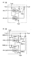
(実施の形態2)
本実施の形態では、実施の形態1で説明した半導体装置100(半導体装置100A)の別の構成例について、説明する。(Embodiment 2)
In this embodiment, another configuration example of the semiconductor device 100 (
図8は、図1の半導体装置100に含まれているトランジスタの極性を入れ換えた場合の半導体装置の構成を示すブロック図である。半導体装置200は、回路201と、調整回路202と、回路203と、回路204と、保持回路SH1と、保持回路SH2と、を有する。 FIG. 8 is a block diagram showing the configuration of the semiconductor device when the polarities of the transistors included in the
回路201は、実施の形態1で説明した回路101に相当する回路であり、端子TLA1乃至端子TLA5を有する。端子TLA1は、保持回路SH1に電気的に接続され、端子TLA2は、配線OUTLに電気的に接続され、端子TLA3は、配線GNDLに電気的に接続され、端子TLA5は、配線VDDLに電気的に接続されている。 A
回路203は、実施の形態1で説明した回路103に相当する回路であり、端子TLC1乃至端子TLC3を有する。端子TLC2は、端子TLA4に電気的に接続され、端子TLC3は、配線VDDLに電気的に接続されている。 A
調整回路202は、実施の形態1で説明した調整回路102に相当する回路であり、端子TLB1乃至端子TLB4を有する。端子TLB1は、保持回路SH2に電気的に接続され、端子TLB2は、端子TLC1に電気的に接続され、端子TLB3は、配線GNDLに電気的に接続され、端子TLB4は、配線VDDLに電気的に接続されている。 The
回路204は、実施の形態1で説明した回路104に相当する回路であり、端子TLD1乃至端子TLD3を有する。端子TLD1は、保持回路SH2に電気的に接続され、端子TLD2は、配線VDD2Lに電気的に接続され、端子TLD3は、配線VDDLに電気的に接続されている。 A
保持回路SH1及び保持回路SH2については、実施の形態1で説明した保持回路SH1及び保持回路SH2の記載を参酌する。また、保持回路SH1のスイッチSW1及び/又は保持回路SH2のスイッチSW2としてトランジスタを適用している場合、半導体装置200における当該トランジスタの極性は、nチャネル型又はpチャネル型のどちらでもよい。そのため、半導体装置200は、前述の通り、半導体装置100に含まれているトランジスタの極性を入れ換えた構成としているが、保持回路SH1及び保持回路SH2についてはこの限りではない。 For the holding circuit SH1 and the holding circuit SH2, the description of the holding circuit SH1 and the holding circuit SH2 in
<<回路201、回路203>>
次に、回路201及び回路203の回路構成について説明する。図9は、回路201及び回路203の回路構成の例を示した図である。<<
Next, circuit configurations of the
図9に示す回路201は、オペアンプOP2を構成する一部の回路素子と、トランジスタTr11と、抵抗素子R11と、抵抗素子R12と、を有する。なお、トランジスタTr11は、pチャネル型トランジスタとする。また、オペアンプOP2はトランジスタTr12乃至トランジスタTr16を有している。なお、トランジスタTr12及びトランジスタTr13は、nチャネル型トランジスタであり、トランジスタTr14乃至トランジスタTr16は、pチャネル型トランジスタである。また、図9に示す回路203は、トランジスタTr16を有する。つまり、図9に示す回路201及び回路203の回路構成の例では、オペアンプOP2は、回路201の一部の回路素子と回路203とによって構成されている。また、この場合、オペアンプOP2は、バイアス電流を生成する機能と、当該バイアス電流によって差動対(トランジスタTr14とトランジスタTr15のそれぞれのゲート)に入力される電位に応じて出力電位を生成する機能と、を有する増幅回路として機能する。 A
トランジスタTr12の第1端子は、端子TLA3に電気的に接続され、トランジスタTr12の第2端子は、トランジスタTr14の第1端子に電気的に接続され、トランジスタTr12のゲートは、トランジスタTr13のゲートと、トランジスタTr13の第2端子と、に電気的に接続されている。トランジスタTr13の第1端子は、端子TLA3に電気的に接続され、トランジスタTr13の第2端子は、トランジスタTr11のゲートと、トランジスタTr15の第1端子と、に電気的に接続されている。 The first terminal of the transistor Tr12 is electrically connected to the terminal TLA3, the second terminal of the transistor Tr12 is electrically connected to the first terminal of the transistor Tr14, the gate of the transistor Tr12 is connected to the gate of the transistor Tr13, It is electrically connected to the second terminal of the transistor Tr13. A first terminal of the transistor Tr13 is electrically connected to the terminal TLA3, and a second terminal of the transistor Tr13 is electrically connected to the gate of the transistor Tr11 and the first terminal of the transistor Tr15.
トランジスタTr14の第2端子は、端子TLA4に電気的に接続され、トランジスタTr14のゲートは、端子TLA1に電気的に接続されている。トランジスタTr15の第2端子は、端子TLA4に電気的に接続され、トランジスタTr15のゲートは、抵抗素子R11の第1端子と、抵抗素子R12の第1端子と、に電気的に接続されている。トランジスタTr16の第1端子は、端子TLC2に電気的に接続され、トランジスタTr16の第2端子は、端子TLC3に電気的に接続され、トランジスタTr16のゲートは、端子TLC1に電気的に接続されている。 A second terminal of the transistor Tr14 is electrically connected to the terminal TLA4, and a gate of the transistor Tr14 is electrically connected to the terminal TLA1. A second terminal of the transistor Tr15 is electrically connected to the terminal TLA4, and a gate of the transistor Tr15 is electrically connected to the first terminal of the resistance element R11 and the first terminal of the resistance element R12. A first terminal of the transistor Tr16 is electrically connected to the terminal TLC2, a second terminal of the transistor Tr16 is electrically connected to the terminal TLC3, and a gate of the transistor Tr16 is electrically connected to the terminal TLC1. .
つまり、トランジスタTr14のゲートは、オペアンプOP2の非反転入力端子に相当し、トランジスタTr15のゲートは、オペアンプOP2の反転入力端子に相当し、トランジスタTr12の第1端子及びトランジスタTr13の第1端子は、オペアンプOP2の低電源電位入力端子に相当し、トランジスタTr16の第2端子は、オペアンプOP2の高電源電位入力端子に相当する。 That is, the gate of the transistor Tr14 corresponds to the non-inverting input terminal of the operational amplifier OP2, the gate of the transistor Tr15 corresponds to the inverting input terminal of the operational amplifier OP2, and the first terminal of the transistor Tr12 and the first terminal of the transistor Tr13 are It corresponds to the low power supply potential input terminal of the operational amplifier OP2, and the second terminal of the transistor Tr16 corresponds to the high power supply potential input terminal of the operational amplifier OP2.
トランジスタTr11の第1端子は、端子TLA3に電気的に接続されている。端子TLA2は、トランジスタTr11の第2端子と、抵抗素子R11の第2端子と、に電気的に接続されている。端子TLA5は、抵抗素子R12の第2端子に電気的に接続されている。 A first terminal of the transistor Tr11 is electrically connected to the terminal TLA3. The terminal TLA2 is electrically connected to the second terminal of the transistor Tr11 and the second terminal of the resistance element R11. The terminal TLA5 is electrically connected to the second terminal of the resistive element R12.
抵抗素子R11、及び抵抗素子R12は、トランジスタTr15に印加するフィードバック電位を生成する役割を有している。そのため、抵抗素子R11及び/又は抵抗素子R12としては、代わりにトランジスタ、ダイオードなどの回路素子を適用することができる。 The resistance element R11 and the resistance element R12 have a role of generating a feedback potential to be applied to the transistor Tr15. Therefore, circuit elements such as transistors and diodes can be used instead of the resistance element R11 and/or the resistance element R12.
回路201及び回路203を図9に示す回路構成にすることによって、オペアンプOP2の非反転入力端子に配線REFLからの参照電位が入力されることで、参照電位に応じた電圧を回路201で生成して、端子TLA2から出力することができる。 By configuring the
なお、図9に示すオペアンプOP2において、低電源電位を与える端子TLA3とトランジスタTr12とトランジスタTr13と、によってカレントミラー回路が構成されており、トランジスタTr14及びトランジスタTr15によって、差動回路が構成されている。したがって、トランジスタTr12及びトランジスタTr13のそれぞれの構造、サイズは互いに同等であることが好ましく、トランジスタTr14及びトランジスタTr15のそれぞれの構造、サイズは互いに同等であることが好ましい。 In the operational amplifier OP2 shown in FIG. 9, the terminal TLA3, which supplies a low power supply potential, the transistors Tr12 and Tr13 form a current mirror circuit, and the transistors Tr14 and Tr15 form a differential circuit. . Therefore, the structures and sizes of the transistors Tr12 and Tr13 are preferably the same, and the structures and the sizes of the transistors Tr14 and Tr15 are preferably the same.
また、トランジスタTr11乃至トランジスタTr15は、特に断りの無い場合は、飽和領域で動作するものとする。つまり、トランジスタTr11乃至トランジスタTr15のゲート電圧、ソース電圧、及びドレイン電圧は、飽和領域で動作する範囲の電圧として適切にバイアスされているものとする。 Further, the transistors Tr11 to Tr15 are assumed to operate in the saturation region unless otherwise specified. In other words, it is assumed that the gate voltage, source voltage, and drain voltage of the transistors Tr11 to Tr15 are appropriately biased as voltages within the range of operation in the saturation region.
なお、回路201及び回路203の具体的な動作については、実施の形態1で説明した回路101及び回路103の記載を参酌する。 Note that the description of the
<<調整回路202>>
調整回路202としては、実施の形態1で説明した、図3に示す調整回路102を適用することができる。この場合、端子TLB1乃至端子TLB4のそれぞれは、端子TLb1乃至端子TLb4に対応する。<<
As the
<<回路203、回路204>>
次に、回路203及び回路204の回路構成について説明する。図10は、回路203及び回路204の回路構成の例を示した図である。なお、回路203及び回路204の接続構成を説明するため、図10では、調整回路202及び保持回路SH2も図示している。<<
Next, circuit configurations of the
回路203は、トランジスタTr16を有し、回路204は、トランジスタTr17と、定電流源CIと、を有している。なお、トランジスタTr16及びトランジスタTr17は、pチャネル型トランジスタとする。 The
トランジスタTr16の第1端子は、端子TLC2に電気的に接続され、トランジスタTr16の第2端子は、端子TLC3に電気的に接続され、トランジスタTr16のゲートは、端子TLC1に電気的に接続されている。トランジスタTr17の第1端子は、定電流源CIの入力端子と、トランジスタTr17のゲートと、に電気的に接続され、トランジスタTr17の第2端子は、端子TLD3に電気的に接続され、トランジスタTr17のゲートは、端子TLD1に電気的に接続されている。定電流源CIの出力端子は、端子TLD2に電気的に接続されている。 A first terminal of the transistor Tr16 is electrically connected to the terminal TLC2, a second terminal of the transistor Tr16 is electrically connected to the terminal TLC3, and a gate of the transistor Tr16 is electrically connected to the terminal TLC1. . A first terminal of the transistor Tr17 is electrically connected to the input terminal of the constant current source CI and the gate of the transistor Tr17, and a second terminal of the transistor Tr17 is electrically connected to the terminal TLD3. The gate is electrically connected to terminal TLD1. The output terminal of constant current source CI is electrically connected to terminal TLD2.
ところで、調整回路202として図3(A)乃至(H)、図4(A)(B)に示す調整回路102を適用したとき、調整回路202の端子TLB1と端子TLB2との間は、電気的に接続されていることになる。つまり、保持回路SH2のスイッチSW2がオン状態となっているとき、回路203の端子TLC1と、回路204の端子TLD1と、の間が導通状態になるため、回路203と回路204とによって、カレントミラー回路が構成される。そのため、トランジスタTr16とトランジスタTr17の構造、サイズは互いに同等であることが好ましい。また、トランジスタTr16及びトランジスタTr17は、特に断りの無い場合は、飽和領域で動作するものとする。つまり、トランジスタTr16及びトランジスタTr17のゲート電圧、ソース電圧、及びドレイン電圧は、トランジスタTr11乃至トランジスタTr15と同様に、飽和領域で動作する範囲の電圧として適切にバイアスされているものとする。 By the way, when the
また、上述したトランジスタTr11乃至トランジスタTr17としては、例えば、Siトランジスタとすることができる。 Si transistors, for example, can be used as the transistors Tr11 to Tr17 described above.
回路201を図9に示す回路構成とし、回路203及び回路204を図10に示す回路構成とし、調整回路202を図6に示す半導体装置100Aに含まれる調整回路102と同様の回路構成とした、半導体装置200Aの構成を図11に示す。 The
半導体装置100Aとの相違点として、半導体装置200Aに含まれている回路204の端子TLD2は、配線GND2Lに電気的に接続されている。 A difference from the
配線GND2Lは、回路204に含まれている、定電流源CIの出力端子に所定の電位を与えるための配線である。なお、当該電位は、配線GNDLが与える低電源電位と等しくてもよい。そのため、端子TLD2は、配線GND2Lでなく、配線GNDLに電気的に接続されていてもよい。 A wiring GND2L is a wiring for applying a predetermined potential to the output terminal of the constant current source CI included in the
半導体装置200Aの動作の説明については、実施の形態1で説明した半導体装置100(半導体装置100A)の動作例の記載を参酌する。つまり、半導体装置200Aは、半導体装置100と同様に、回路201のスタートアップ時間を調整することができる。 For the description of the operation of the
なお、本実施の形態は、本明細書で示す他の実施の形態、又は実施例と適宜組み合わせることができる。 Note that this embodiment can be combined with any of the other embodiments or examples described in this specification as appropriate.
(実施の形態3)
本実施の形態では、実施の形態1で説明した半導体装置100、半導体装置100A、実施の形態2で説明した半導体装置200などの断面構成例について説明する。なお、本実施の形態では、半導体装置100、半導体装置100A、実施の形態2で説明した半導体装置200などを包括して、半導体装置300と呼称する。(Embodiment 3)
In this embodiment, cross-sectional configuration examples of the
<半導体装置の構造例>
図12に、半導体装置300の一部の断面を示す。図12に示す半導体装置300は、基板231上に、層310および層320を積層している。図12では、基板231として単結晶半導体基板(例えば、単結晶シリコン基板)を用いる場合を示している。<Structure example of semiconductor device>
FIG. 12 shows a cross section of part of the
〔層310〕
図12において、層310は、基板231上にトランジスタ233a、トランジスタ233b、およびトランジスタ233cを有する。図12では、トランジスタ233a、トランジスタ233b、およびトランジスタ233cのチャネル長方向の断面を示している。[Layer 310]
12,
トランジスタ233a、トランジスタ233b、およびトランジスタ233cのチャネルは、基板231の一部に形成される。集積回路に高速動作が求められる場合は、基板231として単結晶半導体基板を用いることが好ましい。 Channels of
トランジスタ233a、トランジスタ233b、およびトランジスタ233cは、素子分離層232によってそれぞれ電気的に分離される。素子分離層の形成は、LOCOS(Local Oxidation of Silicon)法や、STI(Shallow Trench Isolation)法などを用いることができる。 The
トランジスタ233a、トランジスタ233b、およびトランジスタ233cは、上記実施の形態に示した、トランジスタTr1乃至トランジスタTr7のいずれかに相当する。トランジスタTr1乃至トランジスタTr7は高いオン電流であり、かつ高速動作の可能なトランジスタであることが望まれるため、トランジスタTr1乃至トランジスタTr7は単結晶シリコン基板に形成されるのが好ましい。 The
また、基板231上に絶縁層234が設けられ、トランジスタ233a、トランジスタ233b、およびトランジスタ233c上に絶縁層235、絶縁層237が設けられ、絶縁層237中に電極238が埋設されている。電極238はコンタクトプラグ236を介してトランジスタ233aのソースまたはドレインの一方と電気的に接続されている。 An insulating
また、電極238および絶縁層237の上に、絶縁層239、絶縁層240、および絶縁層241が設けられ、絶縁層239、絶縁層240、および絶縁層241の中に電極242が埋設されている。電極242は、電極238と電気的に接続される。 In addition, an insulating
また、電極242および絶縁層241の上に、絶縁層243、および絶縁層244が設けられ、絶縁層243、および絶縁層244の中に電極245が埋設されている。電極245は、電極242と電気的に接続される。 An insulating
また、電極245および絶縁層244の上に、絶縁層246および絶縁層247が設けられ、絶縁層246および絶縁層247の中に電極249が埋設されている。電極249は、電極245と電気的に接続される。 An insulating
また、電極249および絶縁層247の上に、絶縁層248および絶縁層250が設けられ、絶縁層248および絶縁層250の中に電極251が埋設されている。電極251は、電極249と電気的に接続される。 An insulating
〔層320〕
層320は、層310上に設けられる。層320は、トランジスタ368a、トランジスタ368b、容量素子369a、および容量素子369bを有する。図12では、トランジスタ368aおよびトランジスタ368bのチャネル長方向の断面を示している。なお、トランジスタ368a、およびトランジスタ368bは、バックゲートを有するトランジスタである。[Layer 320]
トランジスタ368a、およびトランジスタ368bは、上記実施の形態に示したトランジスタOTr1、トランジスタOTr2に相当する。よって、トランジスタ368a、およびトランジスタ368bの半導体層に、金属酸化物の一種である酸化物半導体を用いることが好ましい。すなわち、トランジスタ368a、およびトランジスタ368bとして、OSトランジスタを用いることが好ましい。 The
トランジスタ368a、およびトランジスタ368bは、絶縁層361および絶縁層362上に設けられている。また、絶縁層362上に絶縁層363および絶縁層364が設けられている。トランジスタ368a、およびトランジスタ368bのバックゲートは、絶縁層363および絶縁層364中に埋設されている。絶縁層364上に、絶縁層365および絶縁層366が設けられている。また、電極367が、絶縁層361乃至絶縁層366中に埋設されている。電極367は、電極251と電気的に接続されている。 The
また、トランジスタ368a、トランジスタ368b、容量素子369a、および容量素子369b上に、絶縁層371、絶縁層372、および絶縁層373が形成され、絶縁層373上に電極375が形成されている。電極375はコンタクトプラグ374を介して電極367と電気的に接続される。 An insulating
また、電極375上に、絶縁層376、絶縁層377、絶縁層378、および絶縁層379が設けられている。また、電極380が、絶縁層376乃至絶縁層379中に埋設されている。電極380は、電極375と電気的に接続されている。 An insulating
また、電極380および絶縁層379の上に、絶縁層381および絶縁層382が設けられている。 An insulating
<構成材料について>
〔基板〕
基板として用いる材料に大きな制限はないが、少なくとも後の加熱処理に耐えうる程度の耐熱性を有していることが必要となる。例えば、基板としてシリコンや炭化シリコンなどを材料とした単結晶半導体基板、多結晶半導体基板、シリコンゲルマニウムなどを材料とした化合物半導体基板等を用いることができる。また、SOI基板や、半導体基板上に歪トランジスタやFIN型トランジスタなどの半導体素子が設けられたものなどを用いることもできる。または、高電子移動度トランジスタ(HEMT:High Electron Mobility Transistor)に適用可能なヒ化ガリウム、ヒ化アルミニウムガリウム、ヒ化インジウムガリウム、窒化ガリウム、リン化インジウム、シリコンゲルマニウムなどを用いてもよい。すなわち、基板は、単なる支持基板に限らず、他のトランジスタなどのデバイスが形成された基板であってもよい。<Constituent materials>
〔substrate〕
There are no particular restrictions on the material used for the substrate, but it is necessary that the material has at least enough heat resistance to withstand subsequent heat treatment. For example, a single crystal semiconductor substrate, a polycrystalline semiconductor substrate, or a compound semiconductor substrate made of silicon germanium or the like can be used as the substrate. Alternatively, an SOI substrate or a semiconductor substrate provided with a semiconductor element such as a strain transistor or a FIN transistor may be used. Alternatively, gallium arsenide, aluminum gallium arsenide, indium gallium arsenide, gallium nitride, indium phosphide, silicon germanium, or the like, which is applicable to a high electron mobility transistor (HEMT), may be used. That is, the substrate is not limited to a mere support substrate, and may be a substrate on which other devices such as transistors are formed.
また、基板として、バリウムホウケイ酸ガラスやアルミノホウケイ酸ガラスなどのガラス基板、セラミック基板、石英基板、サファイア基板などを用いることもできる。なお、基板として、可撓性基板を用いてもよい。可撓性基板を用いる場合、可撓性基板上に、トランジスタや容量素子などを直接作製してもよいし、他の作製基板上にトランジスタや容量素子などを作製し、その後可撓性基板に剥離、転置してもよい。なお、作製基板から可撓性基板に剥離、転置するために、作製基板とトランジスタや容量素子などとの間に剥離層を設けるとよい。 Further, as the substrate, a glass substrate such as barium borosilicate glass or aluminoborosilicate glass, a ceramic substrate, a quartz substrate, a sapphire substrate, or the like can be used. Note that a flexible substrate may be used as the substrate. When a flexible substrate is used, a transistor, a capacitor, or the like may be directly manufactured over the flexible substrate, or a transistor, a capacitor, or the like may be manufactured over another manufacturing substrate and then overlaid on the flexible substrate. It may be peeled off and transferred. Note that a separation layer is preferably provided between the formation substrate and the transistor, the capacitor, or the like in order to separate and transfer the layers from the formation substrate to the flexible substrate.
可撓性基板としては、例えば、金属、合金、樹脂もしくはガラス、またはそれらの繊維などを用いることができる。基板に用いる可撓性基板は、線膨張率が低いほど環境による変形が抑制されて好ましい。基板に用いる可撓性基板は、例えば、線膨張率が1×10- 3/K以下、5×10-5/K以下、または1×10-5/K以下である材質を用いればよい。樹脂としては、例えば、ポリエステル、ポリオレフィン、ポリアミド(ナイロン、アラミドなど)、ポリイミド、ポリカーボネート、アクリルなどがある。特に、アラミドは、線膨張率が低いため、可撓性基板として好適である。As the flexible substrate, for example, metal, alloy, resin, glass, or fibers thereof can be used. The flexible substrate used for the substrate preferably has a lower coefficient of linear expansion because deformation due to the environment is suppressed. The flexible substrate used for the substrate may be made of a material having a coefficient of linear expansion of 1×10 −3 / K or less, 5×10 −5 /K or less, or 1×10 −5 /K or less. Examples of resin include polyester, polyolefin, polyamide (nylon, aramid, etc.), polyimide, polycarbonate, and acrylic. In particular, aramid is suitable as a flexible substrate because it has a low coefficient of linear expansion.
〔絶縁層〕
絶縁層は、窒化アルミニウム、酸化アルミニウム、窒化酸化アルミニウム、酸化窒化アルミニウム、酸化マグネシウム、窒化シリコン、酸化シリコン、窒化酸化シリコン、酸化窒化シリコン、酸化ガリウム、酸化ゲルマニウム、酸化イットリウム、酸化ジルコニウム、酸化ランタン、酸化ネオジム、酸化ハフニウム、酸化タンタル、アルミニウムシリケートなどから選ばれた材料を、単層でまたは積層して用いる。また、酸化物材料、窒化物材料、酸化窒化物材料、窒化酸化物材料のうち、複数の材料を混合した材料を用いてもよい。[Insulating layer]
The insulating layer includes aluminum nitride, aluminum oxide, aluminum nitride oxide, aluminum oxynitride, magnesium oxide, silicon nitride, silicon oxide, silicon nitride oxide, silicon oxynitride, gallium oxide, germanium oxide, yttrium oxide, zirconium oxide, lanthanum oxide, A material selected from neodymium oxide, hafnium oxide, tantalum oxide, aluminum silicate, etc. is used as a single layer or as a laminate. Alternatively, a material obtained by mixing a plurality of materials selected from oxide materials, nitride materials, oxynitride materials, and nitride oxide materials may be used.
なお、本明細書等において、窒化酸化物とは、酸素よりも窒素の含有量が多い化合物をいう。また、酸化窒化物とは、窒素よりも酸素の含有量が多い化合物をいう。なお、各元素の含有量は、例えば、ラザフォード後方散乱法(RBS:Rutherford Backscattering Spectrometry)等を用いて測定することができる。 Note that in this specification and the like, a nitrided oxide refers to a compound containing more nitrogen than oxygen. An oxynitride is a compound containing more oxygen than nitrogen. The content of each element can be measured using, for example, Rutherford Backscattering Spectrometry (RBS).
また、半導体層として金属酸化物の一種である酸化物半導体を用いる場合は、半導体層中の水素濃度の増加を防ぐために、絶縁層中の水素濃度を低減することが好ましい。具体的には、絶縁層中の水素濃度を、二次イオン質量分析法(SIMS:Secondary
Ion Mass Spectrometry)において2×10²⁰atoms/cm3以下、好ましくは5×1019atoms/cm3以下、より好ましくは1×101
9atoms/cm3以下、さらに好ましくは5×1018atoms/cm3以下とする。特に、半導体層と接する絶縁層の水素濃度を低減することが好ましい。In the case where an oxide semiconductor, which is a type of metal oxide, is used for the semiconductor layer, the hydrogen concentration in the insulating layer is preferably reduced in order to prevent an increase in the hydrogen concentration in the semiconductor layer. Specifically, the hydrogen concentration in the insulating layer is measured by secondary ion mass spectrometry (SIMS).
2×10 20 atoms/cm 3 or less, preferably 5×10 19 atoms/cm 3 or less, more preferably 1 ×10 19 atoms/cm 3 or less, further preferably 5×10 18 atoms/
また、半導体層中の窒素濃度の増加を防ぐために、絶縁層中の窒素濃度を低減することが好ましい。具体的には、絶縁層中の窒素濃度を、SIMSにおいて5×10¹⁹atoms/cm3以下、好ましくは5×1018atoms/cm3以下、より好ましくは1×1018atoms/cm3以下、さらに好ましくは5×1017atoms/cm3以下とする。Also, in order to prevent an increase in nitrogen concentration in the semiconductor layer, it is preferable to reduce the nitrogen concentration in the insulating layer. Specifically, the nitrogen concentration in the insulating layer is 5×10 19 atoms/cm 3 or less, preferably 5×10 18 atoms/cm 3 or less, more preferably 1×10 18 atoms/cm 3 or less by SIMS, More preferably, it is 5×10 17 atoms/cm 3 or less.
また、絶縁層の少なくとも半導体層と接する領域は、欠陥が少ないことが好ましく、代表的には、電子スピン共鳴法(ESR:Electron Spin Resonance)で観察されるシグナルが少ない方が好ましい。例えば、上述のシグナルとしては、g値が2.001に観察されるE’センターが挙げられる。なお、E’センターは、シリコンのダングリングボンドに起因する。例えば、絶縁層として、酸化シリコン層または酸化窒化シリコン層を用いる場合、E’センター起因のスピン密度が、3×10¹⁷spins/cm3以下、好ましくは5×1016spins/cm3以下である酸化シリコン層または酸化窒化シリコン層を用いればよい。In addition, at least the region of the insulating layer in contact with the semiconductor layer preferably has few defects, and typically, it preferably has few signals observed by electron spin resonance (ESR). For example, the signals mentioned above include the E' center observed at a g-value of 2.001. Note that the E' center is due to a dangling bond of silicon. For example, when a silicon oxide layer or a silicon oxynitride layer is used as the insulating layer, the spin density due to the E′ center is 3×10 17 spins/cm 3 or less, preferably 5×10 16 spins/cm 3 or less. A silicon oxide layer or a silicon oxynitride layer may be used.
また、上述のシグナル以外に二酸化窒素(NO2)に起因するシグナルが観察される場合がある。当該シグナルは、Nの核スピンにより3つのシグナルに分裂しており、それぞれのg値が2.037以上2.039以下(第1のシグナルとする)、g値が2.001以上2.003以下(第2のシグナルとする)、およびg値が1.964以上1.966以下(第3のシグナルとする)に観察される。In addition to the signals described above, a signal due to nitrogen dioxide (NO 2 ) may be observed. The signal is split into three signals by the nuclear spin of N, each having a g value of 2.037 or more and 2.039 or less (referred to as the first signal) and a g value of 2.001 or more and 2.003. below (referred to as the second signal) and g values of 1.964 to 1.966 (referred to as the third signal).
例えば、絶縁層として、二酸化窒素(NO2)に起因するシグナルのスピン密度が、1×10¹⁷spins/cm3以上1×1018spins/cm3未満である絶縁層を用いると好適である。For example, it is preferable to use an insulating layer in which the spin density of a signal caused by nitrogen dioxide (NO 2 ) is 1×10 17 spins/cm 3 or more and less than 1×10 18 spins/cm 3 .
なお、二酸化窒素(NO2)を含む窒素酸化物(NOx)は、絶縁層中に準位を形成する。当該準位は、酸化物半導体層のエネルギーギャップ内に位置する。そのため、窒素酸化物(NOx)が、絶縁層と酸化物半導体層の界面に拡散すると、当該準位が絶縁層側において電子をトラップする場合がある。この結果、トラップされた電子が、絶縁層と酸化物半導体層の界面近傍に留まるため、トランジスタのしきい値電圧をプラス方向にシフトさせてしまう。したがって、絶縁層として窒素酸化物の含有量が少ない膜を用いると、トランジスタのしきい値電圧のシフトを低減することができる。Nitrogen oxide (NO x ) including nitrogen dioxide (NO 2 ) forms a level in the insulating layer. The level is located within the energy gap of the oxide semiconductor layer. Therefore, when nitrogen oxide (NO x ) diffuses into the interface between the insulating layer and the oxide semiconductor layer, the level may trap electrons on the insulating layer side. As a result, the trapped electrons stay near the interface between the insulating layer and the oxide semiconductor layer, which shifts the threshold voltage of the transistor in the positive direction. Therefore, by using a film containing a small amount of nitrogen oxide as the insulating layer, the shift of the threshold voltage of the transistor can be reduced.
窒素酸化物(NOx)の放出量が少ない絶縁層としては、例えば、酸化窒化シリコン層を用いることができる。当該酸化窒化シリコン層は、昇温脱離ガス分析法(TDS:Thermal Desorption Spectroscopy)において、窒素酸化物(NOx)の放出量よりアンモニアの放出量が多い膜であり、代表的にはアンモニアの放出量が1×1018cm-3以上5×1019cm-3以下である。なお、上記のアンモニアの放出量は、TDSにおける加熱処理の温度が50℃以上650℃以下、または50℃以上550℃以下の範囲での総量である。For example, a silicon oxynitride layer can be used as the insulating layer that releases a small amount of nitrogen oxides (NO x ). The silicon oxynitride layer is a film that releases more ammonia than nitrogen oxides (NO x ) in thermal desorption spectroscopy (TDS), typically ammonia. The emission amount is 1×10 18 cm −3 or more and 5×10 19 cm −3 or less. The amount of released ammonia is the total amount when the temperature of the heat treatment in TDS is 50° C. or higher and 650° C. or lower, or 50° C. or higher and 550° C. or lower.
窒素酸化物(NOx)は、加熱処理においてアンモニアおよび酸素と反応するため、アンモニアの放出量が多い絶縁層を用いることで窒素酸化物(NOx)が低減される。Since nitrogen oxides (NO x ) react with ammonia and oxygen during heat treatment, nitrogen oxides (NO x ) are reduced by using an insulating layer that releases a large amount of ammonia.
また、酸化物半導体層に接する絶縁層のうち少なくとも1つは、加熱により酸素が放出される絶縁層を用いて形成することが好ましい。具体的には、絶縁層の表面温度が100℃以上700℃以下、好ましくは100℃以上500℃以下の加熱処理で行われるTDSにて、酸素原子に換算した酸素の脱離量が1.0×10¹⁸atoms/cm3以上、1.0×1019atoms/cm3以上、または1.0×1020atoms/cm3以上である絶縁層を用いることが好ましい。なお、本明細書などにおいて、加熱により放出される酸素を「過剰酸素」ともいう。At least one of the insulating layers in contact with the oxide semiconductor layer is preferably formed using an insulating layer from which oxygen is released by heating. Specifically, in TDS performed by heat treatment at a surface temperature of the insulating layer of 100° C. to 700° C., preferably 100° C. to 500° C., the amount of oxygen released in terms of oxygen atoms is 1.0. An insulating layer with a density of 1.0 x 10¹⁹ atoms/ cm3 or more , or 1.0 x 10²⁰ atoms/ cm3 or more is preferably used. Note that in this specification and the like, oxygen released by heating is also referred to as “excess oxygen”.
また、過剰酸素を含む絶縁層は、絶縁層に酸素を添加する処理を行って形成することもできる。酸素を添加する処理は、酸化性雰囲気下における熱処理やプラズマ処理などで行なうことができる。または、イオン注入法、イオンドーピング法、プラズマイマージョンイオン注入法などを用いて酸素を添加してもよい。酸素を添加する処理に用いるガスとしては、16O2もしくは18O2などの酸素ガス、亜酸化窒素ガス、またはオゾンガスなどの、酸素を含むガスが挙げられる。なお、本明細書では酸素を添加する処理を「酸素ドープ処理」ともいう。酸素ドープ処理は、基板を加熱して行なってもよい。Alternatively, the insulating layer containing excess oxygen can be formed by performing treatment for adding oxygen to the insulating layer. The treatment for adding oxygen can be performed by heat treatment, plasma treatment, or the like in an oxidizing atmosphere. Alternatively, oxygen may be added by an ion implantation method, an ion doping method, a plasma immersion ion implantation method, or the like. The gas used for the oxygen-adding treatment includes an oxygen-containing gas such as oxygen gas such as 16 O 2 or 18 O 2 , nitrous oxide gas, or ozone gas. Note that the treatment of adding oxygen is also referred to as “oxygen doping treatment” in this specification. The oxygen doping treatment may be performed by heating the substrate.
また、絶縁層として、ポリイミド、アクリル系樹脂、ベンゾシクロブテン系樹脂、ポリアミド、エポキシ系樹脂等の、耐熱性を有する有機材料を用いることができる。また上記有機材料の他に、低誘電率材料(low-k材料)、シロキサン系樹脂、PSG(リンガラス)、BPSG(リンボロンガラス)等を用いることができる。なお、これらの材料で形成される絶縁層を複数積層させることで、絶縁層を形成してもよい。 For the insulating layer, a heat-resistant organic material such as polyimide, acrylic resin, benzocyclobutene resin, polyamide, or epoxy resin can be used. In addition to the above organic materials, low dielectric constant materials (low-k materials), siloxane-based resins, PSG (phosphorus glass), BPSG (boron boron glass), and the like can be used. Note that the insulating layer may be formed by stacking a plurality of insulating layers formed using these materials.
なおシロキサン系樹脂とは、シロキサン系材料を出発材料として形成されたSi-O-Si結合を含む樹脂に相当する。シロキサン系樹脂は置換基としては有機基(例えばアルキル基やアリール基)やフルオロ基を用いても良い。また、有機基はフルオロ基を有していても良い。 Note that the siloxane-based resin corresponds to a resin containing a Si—O—Si bond formed using a siloxane-based material as a starting material. The siloxane-based resin may use an organic group (for example, an alkyl group or an aryl group) or a fluoro group as a substituent. Moreover, the organic group may have a fluoro group.
絶縁層の形成方法は、特に限定されない。なお、絶縁層に用いる材料によっては焼成工程が必要な場合がある。この場合、絶縁層の焼成工程と他の熱処理工程を兼ねることで、効率よくトランジスタを作製することが可能となる。 A method for forming the insulating layer is not particularly limited. Note that a firing process may be required depending on the material used for the insulating layer. In this case, a transistor can be manufactured efficiently by combining the baking step of the insulating layer with another heat treatment step.
〔電極〕
電極を形成するための導電性材料としては、アルミニウム、クロム、銅、銀、金、白金、タンタル、ニッケル、チタン、モリブデン、タングステン、ハフニウム、バナジウム、ニオブ、マンガン、マグネシウム、ジルコニウム、ベリリウム、インジウムなどから選ばれた金属元素を1種以上含む材料を用いることができる。また、リン等の不純物元素を含有させた多結晶シリコンに代表される、電気伝導度が高い半導体、ニッケルシリサイドなどのシリサイドを用いてもよい。〔electrode〕
Conductive materials for forming electrodes include aluminum, chromium, copper, silver, gold, platinum, tantalum, nickel, titanium, molybdenum, tungsten, hafnium, vanadium, niobium, manganese, magnesium, zirconium, beryllium, indium, etc. A material containing one or more metal elements selected from can be used. Alternatively, a semiconductor with high electrical conductivity, typified by polycrystalline silicon containing an impurity element such as phosphorus, or a silicide such as nickel silicide may be used.
また、上記の金属元素および酸素を含む導電性材料を用いてもよい。また、上記の金属元素および窒素を含む導電性材料を用いてもよい。例えば、窒化チタン、窒化タンタルなどの窒素を含む導電性材料を用いてもよい。また、インジウム錫酸化物(ITO:Indium Tin Oxide)、酸化タングステンを含むインジウム酸化物、酸化タングステンを含むインジウム亜鉛酸化物、酸化チタンを含むインジウム酸化物、酸化チタンを含むインジウム錫酸化物、インジウム亜鉛酸化物、インジウムガリウム亜鉛酸化物、シリコンを添加したインジウム錫酸化物を用いてもよい。また、窒素を含むインジウムガリウム亜鉛酸化物を用いてもよい。 Alternatively, a conductive material containing any of the above metal elements and oxygen may be used. Alternatively, a conductive material containing the above metal element and nitrogen may be used. For example, a conductive material containing nitrogen such as titanium nitride or tantalum nitride may be used. Indium tin oxide (ITO), indium oxide containing tungsten oxide, indium zinc oxide containing tungsten oxide, indium oxide containing titanium oxide, indium tin oxide containing titanium oxide, indium zinc Oxides, indium gallium zinc oxide, and silicon-doped indium tin oxide may also be used. Alternatively, indium gallium zinc oxide containing nitrogen may be used.
また、上記の材料で形成される導電層を複数積層して用いてもよい。例えば、前述した金属元素を含む材料と、酸素を含む導電性材料と、を組み合わせた積層構造としてもよい。また、前述した金属元素を含む材料と、窒素を含む導電性材料と、を組み合わせた積層構造としてもよい。また、前述した金属元素を含む材料と、酸素を含む導電性材料と、窒素を含む導電性材料と、を組み合わせた積層構造としてもよい。また、窒素を含む導電性材料と、酸素を含む導電性材料と、を組み合わせた積層構造としてもよい。 Alternatively, a plurality of conductive layers formed using any of the above materials may be stacked and used. For example, a laminated structure in which the material containing the metal element described above and the conductive material containing oxygen are combined may be used. Alternatively, a laminated structure may be employed in which the material containing the metal element described above and the conductive material containing nitrogen are combined. Alternatively, a laminated structure may be employed in which the material containing the metal element described above, the conductive material containing oxygen, and the conductive material containing nitrogen are combined. Alternatively, a layered structure in which a conductive material containing nitrogen and a conductive material containing oxygen are combined may be employed.
なお、半導体層に酸化物半導体を用いて、ゲート電極として前述した金属元素を含む材料と、酸素を含む導電性材料と、を組み合わせた積層構造を用いる場合は、酸素を含む導電性材料を半導体層側に設けるとよい。酸素を含む導電性材料を半導体層側に設けることで、当該導電性材料から離脱した酸素が半導体層に供給されやすくなる。 Note that in the case where an oxide semiconductor is used for the semiconductor layer and a stacked structure in which the above-described material containing the metal element and the conductive material containing oxygen are combined for the gate electrode, the conductive material containing oxygen is used as the semiconductor. It should be provided on the layer side. By providing the conductive material containing oxygen on the semiconductor layer side, oxygen separated from the conductive material is easily supplied to the semiconductor layer.
なお、電極としては、例えば、タングステン、ポリシリコン等の埋め込み性の高い導電性材料を用いればよい。また、埋め込み性の高い導電性材料と、チタン層、窒化チタン層、窒化タンタル層などのバリア層(拡散防止層)を組み合わせて用いてもよい。なお、電極を「コンタクトプラグ」という場合がある。 As the electrode, for example, a conductive material having a high embedding property such as tungsten or polysilicon may be used. Alternatively, a conductive material with high embeddability and a barrier layer (diffusion prevention layer) such as a titanium layer, a titanium nitride layer, or a tantalum nitride layer may be used in combination. In addition, an electrode may be called a "contact plug."
特に、ゲート絶縁体と接する電極に不純物が透過しにくい導電性材料を用いることが好ましい。不純物が透過しにくい導電性材料として、例えば窒化タンタルが挙げられる。 In particular, it is preferable to use a conductive material through which impurities hardly permeate the electrode in contact with the gate insulator. An example of a conductive material through which impurities are difficult to permeate is tantalum nitride.
絶縁層に不純物が透過しにくい絶縁性材料を用い、電極に不純物が透過しにくい導電性材料を用いることで、トランジスタへの不純物の拡散をさらに抑制することができる。よって、トランジスタの信頼性をさらに高めることができる。すなわち、半導体装置の信頼性をさらに高めることができる。 By using an insulating material through which impurities hardly permeate for the insulating layer and a conductive material through which impurities hardly permeate for the electrodes, diffusion of impurities into the transistor can be further suppressed. Therefore, the reliability of the transistor can be further improved. That is, the reliability of the semiconductor device can be further improved.
〔半導体層〕
半導体層として、単結晶半導体、多結晶半導体、微結晶半導体、または非晶質半導体などを、単体でまたは組み合わせて用いることができる。半導体材料としては、例えば、シリコンや、ゲルマニウムなどを用いることができる。また、シリコンゲルマニウム、炭化シリコン、ガリウムヒ素、酸化物半導体、窒化物半導体などの化合物半導体や、有機半導体などを用いることができる。[Semiconductor layer]
For the semiconductor layer, a single crystal semiconductor, a polycrystalline semiconductor, a microcrystalline semiconductor, an amorphous semiconductor, or the like can be used alone or in combination. For example, silicon, germanium, or the like can be used as the semiconductor material. Compound semiconductors such as silicon germanium, silicon carbide, gallium arsenide, oxide semiconductors, and nitride semiconductors, organic semiconductors, and the like can also be used.
また、半導体層として有機物半導体を用いる場合は、芳香環をもつ低分子有機材料やπ電子共役系導電性高分子などを用いることができる。例えば、ルブレン、テトラセン、ペンタセン、ペリレンジイミド、テトラシアノキノジメタン、ポリチオフェン、ポリアセチレン、ポリパラフェニレンビニレンなどを用いることができる。 Further, when an organic semiconductor is used as the semiconductor layer, a low-molecular-weight organic material having an aromatic ring, a π-electron conjugated conductive polymer, or the like can be used. For example, rubrene, tetracene, pentacene, perylene diimide, tetracyanoquinodimethane, polythiophene, polyacetylene, polyparaphenylenevinylene and the like can be used.
なお、半導体層を積層してもよい。半導体層を積層する場合は、それぞれ異なる結晶状態を有する半導体を用いてもよいし、それぞれ異なる半導体材料を用いてもよい。 In addition, you may laminate|stack a semiconductor layer. When semiconductor layers are stacked, semiconductors having different crystal states may be used, or different semiconductor materials may be used.
また、金属酸化物の一種である酸化物半導体のバンドギャップは2eV以上あるため、半導体層に酸化物半導体を用いると、オフ電流が極めて少ないトランジスタを実現することができる。具体的には、ソースとドレイン間の電圧が3.5V、室温(代表的には25℃)下において、チャネル幅1μm当たりのオフ電流を1×10-20A未満、1×10 -22A未満、あるいは1×10-24A未満とすることができる。すなわち、オンオフ比を20桁以上とすることもできる。また、半導体層に酸化物半導体を用いたトランジスタ(OSトランジスタ)は、ソースとドレイン間の絶縁耐圧が高い。よって、信頼性の良好なトランジスタを提供できる。また、出力電圧が大きく高耐圧なトランジスタを提供できる。また、信頼性の良好な半導体装置などを提供できる。また、出力電圧が大きく高耐圧な半導体装置を提供することができる。 Further, since an oxide semiconductor, which is a kind of metal oxide, has a bandgap of 2 eV or more, a transistor with extremely low off-state current can be obtained by using an oxide semiconductor for a semiconductor layer. Specifically, at a source-drain voltage of 3.5 V and at room temperature (typically 25° C.), the off current per 1 μm channel width is 1×10.-20Less than A, 1 x 10 -22Less than A or 1 x 10-24It can be less than A. That is, the on/off ratio can be made 20 digits or more. A transistor including an oxide semiconductor for a semiconductor layer (OS transistor) has high withstand voltage between a source and a drain. Therefore, a highly reliable transistor can be provided. Further, a transistor with high output voltage and high withstand voltage can be provided. In addition, a highly reliable semiconductor device or the like can be provided. Further, a semiconductor device with high output voltage and high withstand voltage can be provided.
また、本明細書等において、チャネルが形成される半導体層に結晶性を有するシリコンを用いたトランジスタを「結晶性Siトランジスタ」ともいう。 In this specification and the like, a transistor using crystalline silicon for a semiconductor layer in which a channel is formed is also referred to as a “crystalline Si transistor”.
結晶性Siトランジスタは、OSトランジスタよりも比較的高い移動度を得やすい。一方で、結晶性Siトランジスタは、OSトランジスタのように極めて少ないオフ電流の実現が困難である。よって、半導体層に用いる半導体材料は、目的や用途に応じて適宜使い分けることが肝要である。例えば、目的や用途に応じて、OSトランジスタと結晶性Siトランジスタなどを組み合わせて用いてもよい。 A crystalline Si transistor tends to obtain relatively higher mobility than an OS transistor. On the other hand, it is difficult for a crystalline Si transistor to achieve an extremely low off-current like an OS transistor. Therefore, it is important to properly use the semiconductor material used for the semiconductor layer according to the purpose and application. For example, an OS transistor and a crystalline Si transistor may be used in combination depending on the purpose and application.
半導体層として酸化物半導体層を用いる場合は、酸化物半導体層をスパッタリング法で形成することが好ましい。酸化物半導体層は、スパッタリング法で形成すると酸化物半導体層の密度を高められるため、好適である。スパッタリング法で酸化物半導体層を形成する場合、スパッタリングガスには、希ガス(代表的にはアルゴン)、酸素、または、希ガスおよび酸素の混合ガスを用いればよい。また、スパッタリングガスの高純度化も必要である。例えば、スパッタリングガスとして用いる酸素ガスや希ガスは、露点が-60℃以下、好ましくは-100℃以下にまで高純度化したガスを用いる。高純度化されたスパッタリングガスを用いて成膜することで、酸化物半導体層に水分等が取り込まれることを可能な限り防ぐことができる。 When an oxide semiconductor layer is used as the semiconductor layer, the oxide semiconductor layer is preferably formed by a sputtering method. An oxide semiconductor layer is preferably formed by a sputtering method because the density of the oxide semiconductor layer can be increased. In the case of forming an oxide semiconductor layer by a sputtering method, a sputtering gas may be a rare gas (typically argon), oxygen, or a mixed gas of a rare gas and oxygen. Also, the sputtering gas must be highly purified. For example, an oxygen gas or a rare gas used as a sputtering gas is highly purified to have a dew point of −60° C. or lower, preferably −100° C. or lower. By forming a film using a highly purified sputtering gas, entry of moisture or the like into the oxide semiconductor layer can be prevented as much as possible.
また、スパッタリング法で酸化物半導体層を形成する場合、スパッタリング装置が有する成膜室内の水分を可能な限り除去することが好ましい。例えば、クライオポンプのような吸着式の真空排気ポンプを用いて、成膜室内を高真空(5×10⁻⁷Paから1×10 -4Pa程度まで)に排気することが好ましい。特に、スパッタリング装置の待機時における、成膜室内のH2Oに相当するガス分子(m/z=18に相当するガス分子)の分圧を1×10-4Pa以下とすることが好ましく、5×10-5Pa以下とすることがより好ましい。 In the case of forming an oxide semiconductor layer by a sputtering method, it is preferable to remove moisture in a deposition chamber of a sputtering apparatus as much as possible. For example, a high vacuum (5×10⁻⁷Pa to 1 x 10 -4up to about Pa). In particular, H2Let the partial pressure of the gas molecule corresponding to O (gas molecule corresponding to m/z = 18) be 1 × 10⁻⁴Pa or less is preferable, 5 × 10⁻⁵Pa or less is more preferable.
〔金属酸化物〕
金属酸化物の一種である酸化物半導体は、少なくともインジウムまたは亜鉛を含むことが好ましい。特にインジウムおよび亜鉛を含むことが好ましい。また、それらに加えて、アルミニウム、ガリウム、イットリウムまたはスズなどが含まれていることが好ましい。また、ホウ素、シリコン、チタン、鉄、ニッケル、ゲルマニウム、ジルコニウム、モリブデン、ランタン、セリウム、ネオジム、ハフニウム、タンタル、タングステン、またはマグネシウムなどから選ばれた一種、または複数種が含まれていてもよい。[Metal oxide]
An oxide semiconductor, which is a type of metal oxide, preferably contains at least indium or zinc. Indium and zinc are particularly preferred. In addition to these, aluminum, gallium, yttrium, tin, or the like is preferably contained. Further, one or more selected from boron, silicon, titanium, iron, nickel, germanium, zirconium, molybdenum, lanthanum, cerium, neodymium, hafnium, tantalum, tungsten, magnesium, etc. may be contained.
ここで、酸化物半導体が、インジウム、元素Mおよび亜鉛を有する場合を考える。なお、元素Mは、アルミニウム、ガリウム、イットリウムまたはスズなどとする。そのほかの元素Mに適用可能な元素として、ホウ素、シリコン、チタン、鉄、ニッケル、ゲルマニウム、ジルコニウム、モリブデン、ランタン、セリウム、ネオジム、ハフニウム、タンタル、タングステン、マグネシウムなどがある。ただし、元素Mとして、前述の元素を複数組み合わせても構わない場合がある。 Now, consider the case where the oxide semiconductor contains indium, the element M, and zinc. Note that the element M is aluminum, gallium, yttrium, tin, or the like. Other elements applicable to element M include boron, silicon, titanium, iron, nickel, germanium, zirconium, molybdenum, lanthanum, cerium, neodymium, hafnium, tantalum, tungsten, and magnesium. However, as the element M, there are cases where a plurality of the above elements may be combined.
なお、本明細書等において、窒素を有する金属酸化物も金属酸化物(metal oxide)と総称する場合がある。また、窒素を有する金属酸化物を、金属酸窒化物(metal oxynitride)と呼称してもよい。 In this specification and the like, metal oxides containing nitrogen may also be collectively referred to as metal oxides. Metal oxides containing nitrogen may also be referred to as metal oxynitrides.
[金属酸化物の構成]
以下では、本発明の一態様で開示されるトランジスタに用いることができるCAC(Cloud-Aligned Composite)-OS、及びCAAC(c-axis
aligned crystalline)-OSについて説明する。[Structure of Metal Oxide]
Below, CAC (Cloud-Aligned Composite)-OS and CAAC (c-axis
aligned crystalline)-OS will be explained.
なお、本明細書等において、CACは機能、または材料の構成の一例を表し、また、CAAC(c-axis aligned crystal)は結晶構造の一例を表す。 Note that in this specification and the like, CAC represents an example of a function or a structure of a material, and CAAC (c-axis aligned crystal) represents an example of a crystal structure.
CAC-OSまたはCAC-metal oxideとは、材料の一部では導電性の機能と、材料の一部では絶縁性の機能とを有し、材料の全体では半導体としての機能を有する。なお、CAC-OSまたはCAC-metal oxideを、トランジスタのチャネル形成領域に含まれている場合、導電性の機能は、キャリアとなる電子(または正孔)を流す機能であり、絶縁性の機能は、キャリアとなる電子を流さない機能である。導電性の機能と、絶縁性の機能とを、それぞれ相補的に作用させることで、スイッチングさせる機能(On/Offさせる機能)をCAC-OSまたはCAC-metal oxideに付与することができる。CAC-OSまたはCAC-metal oxideにおいて、それぞれの機能を分離させることで、双方の機能を最大限に高めることができる。 CAC-OS or CAC-metal oxide has a conductive function in a part of the material, an insulating function in a part of the material, and a semiconductor function in the whole material. Note that when CAC-OS or CAC-metal oxide is included in the channel formation region of a transistor, the function of conductivity is to flow electrons (or holes) that serve as carriers, and the function of insulation is to flow. , is a function that does not flow electrons that serve as carriers. A switching function (on/off function) can be imparted to the CAC-OS or CAC-metal oxide by causing the conductive function and the insulating function to act complementarily. By separating each function in CAC-OS or CAC-metal oxide, both functions can be maximized.
また、CAC-OSまたはCAC-metal oxideは、導電性領域、および絶縁性領域を有する。導電性領域は、上述の導電性の機能を有し、絶縁性領域は、上述の絶縁性の機能を有する。また、材料中において、導電性領域と、絶縁性領域とは、ナノ粒子レベルで分離している場合がある。また、導電性領域と、絶縁性領域とは、それぞれ材料中に偏在する場合がある。また、導電性領域は、周辺がぼけてクラウド状に連結して観察される場合がある。 CAC-OS or CAC-metal oxide also has a conductive region and an insulating region. The conductive regions have the above-described conductive function, and the insulating regions have the above-described insulating function. In some materials, the conductive region and the insulating region are separated at the nanoparticle level. Also, the conductive region and the insulating region may be unevenly distributed in the material. In addition, the conductive region may be observed to be connected like a cloud with its periphery blurred.
また、CAC-OSまたはCAC-metal oxideにおいて、導電性領域と、絶縁性領域とは、それぞれ0.5nm以上10nm以下、好ましくは0.5nm以上3nm以下のサイズで材料中に分散している場合がある。 In CAC-OS or CAC-metal oxide, the conductive region and the insulating region are each dispersed in the material with a size of 0.5 nm or more and 10 nm or less, preferably 0.5 nm or more and 3 nm or less. There is
また、CAC-OSまたはCAC-metal oxideは、異なるバンドギャップを有する成分により構成される。例えば、CAC-OSまたはCAC-metal oxideは、絶縁性領域に起因するワイドギャップを有する成分と、導電性領域に起因するナローギャップを有する成分と、により構成される。当該構成の場合、キャリアを流す際に、ナローギャップを有する成分において、主にキャリアが流れる。また、ナローギャップを有する成分が、ワイドギャップを有する成分に相補的に作用し、ナローギャップを有する成分に連動してワイドギャップを有する成分にもキャリアが流れる。このため、上記CAC-OSまたはCAC-metal oxideをトランジスタのチャネル形成領域に用いる場合、トランジスタのオン状態において高い電流駆動力、つまり大きなオン電流、および高い電界効果移動度を得ることができる。 Also, CAC-OS or CAC-metal oxide is composed of components having different bandgaps. For example, CAC-OS or CAC-metal oxide is composed of a component having a wide gap resulting from an insulating region and a component having a narrow gap resulting from a conductive region. In the case of this configuration, when the carriers flow, the carriers mainly flow in the component having the narrow gap. In addition, the component having a narrow gap acts complementarily on the component having a wide gap, and carriers also flow into the component having a wide gap in conjunction with the component having a narrow gap. Therefore, when the above CAC-OS or CAC-metal oxide is used for a channel formation region of a transistor, high current drivability, that is, large on-current and high field-effect mobility can be obtained in the on-state of the transistor.
すなわち、CAC-OSまたはCAC-metal oxideは、マトリックス複合材(matrix composite)、または金属マトリックス複合材(metal
matrix composite)と呼称することもできる。That is, CAC-OS or CAC-metal oxide is a matrix composite or a metal matrix composite.
It can also be called a matrix composite).
[金属酸化物の構造]
金属酸化物の一種である酸化物半導体は、単結晶酸化物半導体と、それ以外の非単結晶酸化物半導体と、に分けられる。非単結晶酸化物半導体としては、例えば、CAAC-OS、多結晶酸化物半導体、nc-OS(nanocrystalline oxide semiconductor)、擬似非晶質酸化物半導体(a-like OS:amorphous-like oxide semiconductor)および非晶質酸化物半導体などがある。[Structure of Metal Oxide]
Oxide semiconductors, which are a type of metal oxide, are classified into single-crystal oxide semiconductors and non-single-crystal oxide semiconductors. Non-single-crystal oxide semiconductors include, for example, CAAC-OS, polycrystalline oxide semiconductors, nanocrystalline oxide semiconductors (nc-OS), amorphous-like oxide semiconductors (a-like OS), and There are amorphous oxide semiconductors and the like.
CAAC-OSは、c軸配向性を有し、かつa-b面方向において複数のナノ結晶が連結し、歪みを有した結晶構造となっている。なお、歪みとは、複数のナノ結晶が連結する領域において、格子配列の揃った領域と、別の格子配列の揃った領域と、の間で格子配列の向きが変化している箇所を指す。 CAAC-OS has a c-axis orientation and a distorted crystal structure in which a plurality of nanocrystals are connected in the ab plane direction. The strain refers to a portion where the orientation of the lattice arrangement changes between a region with a uniform lattice arrangement and another region with a uniform lattice arrangement in a region where a plurality of nanocrystals are connected.
ナノ結晶は、六角形を基本とするが、正六角形状とは限らず、非正六角形状である場合がある。また、歪みにおいて、五角形、七角形などの格子配列を有する場合がある。なお、CAAC-OSにおいて、歪み近傍においても、明確な結晶粒界(グレインバウンダリーともいう。)を確認することは難しい。すなわち、格子配列の歪みによって、結晶粒界の形成が抑制されていることがわかる。これは、CAAC-OSが、a-b面方向において酸素原子の配列が稠密でないことや、金属元素が置換することで原子間の結合距離が変化することなどによって、歪みを許容することができるためである。 Although nanocrystals are basically hexagonal, they are not limited to regular hexagons and may have non-regular hexagons. In some cases, the strain has a lattice arrangement of pentagons, heptagons, or the like. In CAAC-OS, it is difficult to confirm clear crystal grain boundaries (also called grain boundaries) even in the vicinity of strain. That is, it can be seen that the distortion of the lattice arrangement suppresses the formation of grain boundaries. This is because the CAAC-OS can tolerate strain due to the fact that the arrangement of oxygen atoms is not dense in the ab plane direction and the bond distance between atoms changes due to the substitution of metal elements. Because.
また、CAAC-OSは、インジウム、および酸素を有する層(以下、In層)と、元素M、亜鉛、および酸素を有する層(以下、(M、Zn)層)とが積層した、層状の結晶構造(層状構造ともいう)を有する傾向がある。なお、インジウムと元素Mは、互いに置換可能であり、(M、Zn)層の元素Mがインジウムと置換した場合、(In、M、Zn)層と表すこともできる。また、In層のインジウムが元素Mと置換した場合、(In、M)層と表すこともできる。 CAAC-OS is a layered crystal in which a layer containing indium and oxygen (hereinafter referred to as an In layer) and a layer containing the element M, zinc, and oxygen (hereinafter referred to as a (M, Zn) layer) are stacked. It tends to have a structure (also called a layered structure). Note that indium and the element M can be substituted with each other, and when the element M in the (M, Zn) layer is substituted with indium, the layer can also be expressed as an (In, M, Zn) layer. Further, when indium in the In layer is replaced with an element M, it can also be expressed as an (In, M) layer.
CAAC-OSは結晶性の高い金属酸化物である。一方、CAAC-OSは、明確な結晶粒界を確認することが難しいため、結晶粒界に起因する電子移動度の低下が起こりにくいといえる。また、金属酸化物の結晶性は不純物の混入や欠陥の生成などによって低下する場合があるため、CAAC-OSは不純物や欠陥(酸素欠損など)の少ない金属酸化物ともいえる。したがって、CAAC-OSを有する金属酸化物は、物理的性質が安定する。そのため、CAAC-OSを有する金属酸化物は熱に強く、信頼性が高い。 CAAC-OS is a highly crystalline metal oxide. On the other hand, in CAAC-OS, since it is difficult to confirm a clear crystal grain boundary, it can be said that the decrease in electron mobility due to the crystal grain boundary is unlikely to occur. In addition, since the crystallinity of a metal oxide may be degraded by contamination with impurities, generation of defects, or the like, CAAC-OS can be said to be a metal oxide with few impurities and defects (such as oxygen vacancies). Therefore, metal oxides with CAAC-OS have stable physical properties. Therefore, a metal oxide containing CAAC-OS is heat resistant and highly reliable.
nc-OSは、微小な領域(例えば、1nm以上10nm以下の領域、特に1nm以上3nm以下の領域)において原子配列に周期性を有する。また、nc-OSは、異なるナノ結晶間で結晶方位に規則性が見られない。そのため、膜全体で配向性が見られない。したがって、nc-OSは、分析方法によっては、a-like OSや非晶質酸化物半導体と区別が付かない場合がある。 The nc-OS has periodic atomic arrangement in a minute region (eg, a region of 1 nm to 10 nm, particularly a region of 1 nm to 3 nm). Also, nc-OS shows no regularity in crystal orientation between different nanocrystals. Therefore, no orientation is observed in the entire film. Therefore, an nc-OS may be indistinguishable from an a-like OS or an amorphous oxide semiconductor depending on the analysis method.
a-like OSは、nc-OSと非晶質酸化物半導体との間の構造を有する金属酸化物である。a-like OSは、鬆または低密度領域を有する。すなわち、a-like OSは、nc-OSおよびCAAC-OSと比べて、結晶性が低い。 An a-like OS is a metal oxide having a structure between an nc-OS and an amorphous oxide semiconductor. An a-like OS has void or low density regions. That is, a-like OS has lower crystallinity than nc-OS and CAAC-OS.
酸化物半導体(金属酸化物)は、多様な構造をとり、それぞれが異なる特性を有する。酸化物半導体は、非晶質酸化物半導体、多結晶酸化物半導体、a-like OS、nc-OS、CAAC-OSのうち、二種以上を有していてもよい。 Oxide semiconductors (metal oxides) have various structures, each of which has different characteristics. The oxide semiconductor may include two or more of an amorphous oxide semiconductor, a polycrystalline oxide semiconductor, an a-like OS, an nc-OS, and a CAAC-OS.
[金属酸化物を有するトランジスタ]
続いて、上記金属酸化物をトランジスタのチャネル形成領域に用いる場合について説明する。[Transistor with Metal Oxide]
Next, the case where the above metal oxide is used for a channel formation region of a transistor will be described.
なお、上記金属酸化物をトランジスタのチャネル形成領域に用いることで、高い電界効果移動度のトランジスタを実現することができる。また、信頼性の高いトランジスタを実現することができる。 Note that by using the above metal oxide for a channel formation region of a transistor, a transistor with high field-effect mobility can be realized. Further, a highly reliable transistor can be realized.
また、トランジスタには、キャリア密度の低い金属酸化物を用いることが好ましい。金属酸化物膜のキャリア密度を低くする場合においては、金属酸化物膜中の不純物濃度を低くし、欠陥準位密度を低くすればよい。本明細書等において、不純物濃度が低く、欠陥準位密度の低いことを高純度真性または実質的に高純度真性という。例えば、金属酸化物は、キャリア密度が8×10¹¹/cm3未満、好ましくは1×1011/cm3未満、さらに好ましくは1×1010/cm3未満であり、1×10-9/cm3以上とすればよい。A metal oxide with low carrier density is preferably used for a transistor. In order to lower the carrier density of the metal oxide film, the impurity concentration in the metal oxide film should be lowered to lower the defect level density. In this specification and the like, a low impurity concentration and a low defect level density are referred to as high-purity intrinsic or substantially high-purity intrinsic. For example, the metal oxide has a carrier density of less than 8×10 11 /cm 3 , preferably less than 1×10 11 /cm 3 , more preferably less than 1×10 10 /cm 3 , and a carrier density of 1×10 −9 /
また、高純度真性または実質的に高純度真性である金属酸化物膜は、欠陥準位密度が低いため、トラップ準位密度も低くなる場合がある。 In addition, since a highly purified intrinsic or substantially highly purified intrinsic metal oxide film has a low defect level density, the trap level density may also be low.
また、金属酸化物のトラップ準位に捕獲された電荷は、消失するまでに要する時間が長く、あたかも固定電荷のように振る舞うことがある。そのため、トラップ準位密度の高い金属酸化物をチャネル形成領域に有するトランジスタは、電気特性が不安定となる場合がある。 In addition, the charge trapped in the trap level of the metal oxide takes a long time to disappear, and may behave like a fixed charge. Therefore, a transistor including a metal oxide with a high trap level density in a channel formation region may have unstable electrical characteristics.
したがって、トランジスタの電気特性を安定にするためには、金属酸化物中の不純物濃度を低減することが有効である。また、金属酸化物中の不純物濃度を低減するためには、近接する膜中の不純物濃度も低減することが好ましい。不純物としては、水素、窒素、アルカリ金属、アルカリ土類金属、鉄、ニッケル、シリコン等がある。 Therefore, in order to stabilize the electrical characteristics of the transistor, it is effective to reduce the impurity concentration in the metal oxide. Moreover, in order to reduce the impurity concentration in the metal oxide, it is preferable to also reduce the impurity concentration in the adjacent film. Impurities include hydrogen, nitrogen, alkali metals, alkaline earth metals, iron, nickel, silicon, and the like.
[不純物]
ここで、金属酸化物中における各不純物の影響について説明する。[impurities]
Here, the effect of each impurity in the metal oxide will be described.
金属酸化物において、第14族元素の一つであるシリコンや炭素が含まれると、金属酸化物において欠陥準位が形成される。このため、金属酸化物におけるシリコンや炭素の濃度と、金属酸化物との界面近傍のシリコンや炭素の濃度(二次イオン質量分析法(SIMS)により得られる濃度)を、2×10¹⁸atoms/cm3以下、好ましくは2×1017atoms/cm3以下とする。If the metal oxide contains silicon or carbon, which is one of the
また、金属酸化物にアルカリ金属またはアルカリ土類金属が含まれると、欠陥準位を形成し、キャリアを生成する場合がある。したがって、アルカリ金属またはアルカリ土類金属が含まれている金属酸化物をチャネル形成領域に用いたトランジスタはノーマリーオン特性となりやすい。このため、金属酸化物中のアルカリ金属またはアルカリ土類金属の濃度を低減することが好ましい。具体的には、SIMSにより得られる金属酸化物中のアルカリ金属またはアルカリ土類金属の濃度を、1×10¹⁸atoms/cm3以下、好ましくは2×1016atoms/cm3以下にする。Further, if the metal oxide contains an alkali metal or an alkaline earth metal, it may form a defect level and generate carriers. Therefore, a transistor in which a metal oxide containing an alkali metal or an alkaline earth metal is used for a channel formation region tends to have normally-on characteristics. Therefore, it is preferable to reduce the concentration of alkali metals or alkaline earth metals in the metal oxide. Specifically, the concentration of the alkali metal or alkaline earth metal in the metal oxide obtained by SIMS is set to 1×10 18 atoms/cm 3 or less, preferably 2×10 16 atoms/cm 3 or less.
また、金属酸化物において、窒素が含まれると、キャリアである電子が生じ、キャリア密度が増加し、n型化しやすい。この結果、窒素が含まれている金属酸化物をチャネル形成領域に用いたトランジスタはノーマリーオン特性となりやすい。したがって、当該金属酸化物において、チャネル形成領域の窒素はできる限り低減されていることが好ましい。例えば、金属酸化物中の窒素濃度は、SIMSにおいて、5×10¹⁹atoms/cm 3未満、好ましくは5×10¹⁸atoms/cm3以下、より好ましくは1×1018atoms/cm3以下、さらに好ましくは5×1017atoms/cm3以下とする。 In addition, when nitrogen is contained in the metal oxide, electrons as carriers are generated, the carrier density increases, and the metal oxide tends to be n-type. As a result, a transistor using a metal oxide containing nitrogen for a channel formation region tends to have normally-on characteristics. Therefore, nitrogen in the channel formation region in the metal oxide is preferably reduced as much as possible. For example, the nitrogen concentration in the metal oxide is 5×10¹⁹atoms/cm 3less than, preferably 5 x 10¹⁸atoms/cm3below, more preferably 1×10¹⁸atoms/cm3below, more preferably 5×10¹⁷atoms/cm3Below.
また、金属酸化物に含まれる水素は、金属原子と結合する酸素と反応して水になるため、酸素欠損を形成する場合がある。当該酸素欠損に水素が入ることで、キャリアである電子が生成される場合がある。また、水素の一部が金属原子と結合する酸素と結合して、キャリアである電子を生成することがある。したがって、水素が含まれている金属酸化物をチャネル形成領域に用いたトランジスタはノーマリーオン特性となりやすい。このため、金属酸化物中の水素はできる限り低減されていることが好ましい。具体的には、金属酸化物において、SIMSにより得られる水素濃度を、1×10²⁰atoms/cm3未満、好ましくは1×1019atoms/cm3未満、より好ましくは5×1018atoms/cm3未満、さらに好ましくは1×1018atoms/cm3未満とする。In addition, since hydrogen contained in the metal oxide reacts with oxygen bonded to the metal atom to become water, oxygen vacancies may be formed. When hydrogen enters the oxygen vacancies, electrons, which are carriers, are generated in some cases. In addition, part of hydrogen may bond with oxygen that bonds with a metal atom to generate an electron, which is a carrier. Therefore, a transistor in which a metal oxide containing hydrogen is used for a channel formation region tends to have normally-on characteristics. Therefore, it is preferable that hydrogen in the metal oxide is reduced as much as possible. Specifically, in the metal oxide, the hydrogen concentration obtained by SIMS is less than 1×10 20 atoms/cm 3 , preferably less than 1×10 19 atoms/cm 3 , more preferably less than 5×10 18 atoms/cm Less than 3 , more preferably less than 1×10 18 atoms/cm 3 .
不純物が十分に低減された金属酸化物をトランジスタのチャネル形成領域に用いることで、安定した電気特性を付与することができる。 By using a metal oxide in which impurities are sufficiently reduced for a channel formation region of a transistor, stable electrical characteristics can be imparted.
<成膜方法について>
絶縁層を形成するための絶縁性材料、電極を形成するための導電性材料、または半導体層を形成するための半導体材料は、スパッタリング法、スピンコート法、CVD(Chemical Vapor Deposition)法(熱CVD法、MOCVD(Metal Organic Chemical Vapor Deposition)法、PECVD(Plasma Enhanced CVD)法、高密度プラズマCVD(High density plasma CVD)法、LPCVD(low pressure CVD)法、APCVD(atmospheric pressure CVD)法等を含む)、ALD(Atomic Layer Deposition)法、MBE(Molecular Beam Epitaxy)法、PLD(Pulsed Laser Deposition)法、ディップ法、スプレー塗布法、液滴吐出法(インクジェット法など)、または、印刷法(スクリーン印刷、オフセット印刷など)を用いて形成することができる。<About film formation method>
An insulating material for forming an insulating layer, a conductive material for forming an electrode, or a semiconductor material for forming a semiconductor layer can be obtained by a sputtering method, a spin coating method, a CVD (Chemical Vapor Deposition) method (thermal CVD). MOCVD (Metal Organic Chemical Vapor Deposition) method, PECVD (Plasma Enhanced CVD) method, high density plasma CVD (High density plasma CVD) method, LPCVD (low pressure CVD) method, APCVD (atmospheric pressure CVD) method, etc. ), ALD (Atomic Layer Deposition) method, MBE (Molecular Beam Epitaxy) method, PLD (Pulsed Laser Deposition) method, dip method, spray coating method, droplet discharge method (inkjet method, etc.), or printing method (screen printing , offset printing, etc.).
プラズマCVD法は、比較的低温で高品質の膜が得られる。MOCVD法、ALD法、または熱CVD法などの、成膜時にプラズマを用いない成膜方法を用いると、被形成面にダメージが生じにくい。例えば、半導体装置に含まれる配線、電極、素子(トランジスタ、容量素子など)などは、プラズマから電荷を受け取ることでチャージアップする場合がある。このとき、蓄積した電荷によって、半導体装置に含まれる配線、電極、素子などが破壊される場合がある。一方、プラズマを用いない成膜方法の場合、こういったプラズマダメージが生じないため、半導体装置の歩留まりを高くすることができる。また、成膜中のプラズマダメージが生じないため、欠陥の少ない膜が得られる。 The plasma CVD method can obtain high quality films at relatively low temperatures. When a film formation method that does not use plasma for film formation, such as MOCVD, ALD, or thermal CVD, the formation surface is less likely to be damaged. For example, wiring, electrodes, elements (transistors, capacitive elements, etc.) included in a semiconductor device may be charged up by receiving charges from plasma. At this time, the accumulated charges may destroy wiring, electrodes, elements, and the like included in the semiconductor device. On the other hand, in the case of a film formation method that does not use plasma, since such plasma damage does not occur, the yield of semiconductor devices can be increased. Moreover, since plasma damage does not occur during film formation, a film with few defects can be obtained.
CVD法およびALD法は、ターゲットなどから放出される粒子が堆積する成膜方法とは異なり、被処理物の表面における反応により膜が形成される成膜方法である。したがって、被処理物の形状の影響を受けにくく、良好な段差被覆性を有する成膜方法である。特に、ALD法は、優れた段差被覆性と、優れた厚さの均一性を有するため、アスペクト比の高い開口部の表面を被覆する場合などに好適である。ただし、ALD法は、比較的成膜速度が遅いため、成膜速度の速いCVD法などの他の成膜方法と組み合わせて用いることが好ましい場合もある。 The CVD method and the ALD method are film forming methods in which a film is formed by a reaction on the surface of the object to be processed, unlike film forming methods in which particles emitted from a target or the like are deposited. Therefore, it is a film forming method which is not easily affected by the shape of the object to be processed and which has good step coverage. In particular, the ALD method has excellent step coverage and excellent thickness uniformity, and is therefore suitable for coating the surface of an opening with a high aspect ratio. However, since the ALD method has a relatively slow film formation rate, it may be preferable to use it in combination with another film formation method, such as the CVD method, which has a high film formation rate.
CVD法およびALD法は、原料ガスの流量比によって、得られる膜の組成を制御することができる。例えば、CVD法およびALD法では、原料ガスの流量比によって、任意の組成の膜を成膜することができる。また、例えば、CVD法およびALD法では、成膜しながら原料ガスの流量比を変化させることによって、組成が連続的に変化した膜を成膜することができる。原料ガスの流量比を変化させながら成膜する場合、複数の成膜室を用いて成膜する場合と比べて、搬送や圧力調整に掛かる時間の分、成膜に掛かる時間を短くすることができる。したがって、半導体装置の生産性を高めることができる場合がある。 In the CVD method and the ALD method, the composition of the film obtained can be controlled by the flow rate ratio of the raw material gases. For example, in the CVD method and the ALD method, it is possible to form a film of any composition depending on the flow rate ratio of source gases. Further, for example, in the CVD method and the ALD method, it is possible to form a film whose composition is continuously changed by changing the flow rate ratio of the source gases while forming the film. When film formation is performed while changing the flow rate ratio of the raw material gases, the time required for film formation can be shortened by the time required for transportation and pressure adjustment, compared to the case where film formation is performed using a plurality of film formation chambers. can. Therefore, productivity of semiconductor devices can be improved in some cases.
なお、ALD法により成膜する場合は、材料ガスとして塩素を含まないガスを用いることが好ましい。 Note that when the film is formed by the ALD method, it is preferable to use a gas that does not contain chlorine as the material gas.
なお、本実施の形態は、本明細書で示す他の実施の形態、又は実施例と適宜組み合わせることができる。 Note that this embodiment can be combined with any of the other embodiments or examples described in this specification as appropriate.
(実施の形態4)
本実施の形態では、上記実施の形態に示した半導体装置などに用いることができるトランジスタの構造例について説明する。(Embodiment 4)
In this embodiment, structural examples of a transistor that can be used for the semiconductor device or the like described in any of the above embodiments will be described.
<トランジスタの構造例1>
図13(A)、(B)および(C)を用いてトランジスタ510Aの構造例を説明する。図13(A)はトランジスタ510Aの上面図である。図13(B)は、図13(A)に一点鎖線L1-L2で示す部位の断面図である。図13(C)は、図13(A)に一点鎖線W1-W2で示す部位の断面図である。なお、図13(A)の上面図では、図の明瞭化のために一部の要素を省いて図示している。<Transistor Structure Example 1>
A structural example of the
図13(A)、(B)および(C)では、トランジスタ510Aと、層間膜として機能する絶縁層511、絶縁層512、絶縁層514、絶縁層516、絶縁層580、絶縁層582、および絶縁層584を示している。また、トランジスタ510Aと電気的に接続し、コンタクトプラグとして機能する導電層546(導電層546a、および導電層546b)と、配線として機能する導電層503と、を示している。 13A, 13B, and 13C, the
トランジスタ510Aは、第1のゲート電極として機能する導電層560(導電層560a、および導電層560b)と、第2のゲート電極として機能する導電層505(導電層505a、および導電層505b)と、第1のゲート絶縁体として機能する絶縁層550と、第2のゲート絶縁体として機能する絶縁層521、絶縁層522、および絶縁層524と、チャネルが形成される領域を有する酸化物530(酸化物530a、酸化物530b、および酸化物530c)と、ソースまたはドレインの一方として機能する導電層542aと、ソースまたはドレインの他方として機能する導電層542bと、絶縁層574とを有する。なお、本明細書等では、導電層542aと、導電層542bと、をまとめて導電層542と記載する。 The
また、図13に示すトランジスタ510Aでは、酸化物530c、絶縁層550、および導電層560が、絶縁層580に設けられた開口部内に、絶縁層574を介して配置される。また、酸化物530c、絶縁層550、および導電層560は、導電層542a、および導電層542bとの間に配置される。 Further, in the
絶縁層511、および絶縁層512は、層間膜として機能する。 The insulating
層間膜としては、酸化シリコン、酸化窒化シリコン、窒化酸化シリコン、酸化アルミニウム、酸化ハフニウム、酸化タンタル、酸化ジルコニウム、チタン酸ジルコン酸鉛(PZT)、チタン酸ストロンチウム(SrTiO3)または(Ba,Sr)TiO3(BST)などの絶縁体を単層または積層で用いることができる。またはこれらの絶縁体に、例えば、酸化アルミニウム、酸化ビスマス、酸化ゲルマニウム、酸化ニオブ、酸化シリコン、酸化チタン、酸化タングステン、酸化イットリウム、酸化ジルコニウムを添加してもよい。またはこれらの絶縁体を窒化処理してもよい。上記の絶縁体に酸化シリコン、酸化窒化シリコンまたは窒化シリコンを積層して用いてもよい。The interlayer film may be silicon oxide, silicon oxynitride, silicon nitride oxide, aluminum oxide, hafnium oxide, tantalum oxide, zirconium oxide, lead zirconate titanate (PZT), strontium titanate (SrTiO 3 ) or (Ba, Sr). Insulators such as TiO 3 (BST) can be used in single layers or stacks. Alternatively, aluminum oxide, bismuth oxide, germanium oxide, niobium oxide, silicon oxide, titanium oxide, tungsten oxide, yttrium oxide, or zirconium oxide may be added to these insulators. Alternatively, these insulators may be nitrided. Silicon oxide, silicon oxynitride, or silicon nitride may be stacked over the above insulator.
例えば、絶縁層511は、水または水素などの不純物が、基板側からトランジスタ510Aに混入するのを抑制するバリア層として機能することが好ましい。したがって、絶縁層511は、水素原子、水素分子、水分子、銅原子などの不純物の拡散を抑制する機能を有する(上記不純物が透過しにくい。)絶縁性材料を用いることが好ましい。または、酸素(例えば、酸素原子、酸素分子などの少なくとも一)の拡散を抑制する機能を有する(上記酸素が透過しにくい。)絶縁性材料を用いることが好ましい。また、例えば、絶縁層511として酸化アルミニウムや窒化シリコンなどを用いてもよい。当該構成により、水素、水などの不純物が絶縁層511よりも基板側からトランジスタ510A側に拡散するのを抑制することができる。 For example, the insulating
例えば、絶縁層512は、絶縁層511よりも誘電率が低いことが好ましい。誘電率が低い材料を層間膜とすることで、配線間に生じる寄生容量を低減することができる。 For example, insulating
導電層503は、絶縁層512に埋め込まれるように形成される。ここで、導電層503の上面の高さと、絶縁層512の上面の高さは同程度にできる。なお導電層503は、単層とする構成について示しているが、本発明はこれに限られるものではない。例えば、導電層503を2層以上の積層構造としてもよい。なお、導電層503は、タングステン、銅、またはアルミニウムを主成分とする導電性が高い導電性材料を用いることが好ましい。 The
トランジスタ510Aにおいて、導電層560は、第1のゲート(トップゲートともいう。)電極として機能する場合がある。また、導電層505は、第2のゲート(ボトムゲートともいう。)電極として機能する場合がある。その場合、導電層505に印加する電位を、導電層560に印加する電位と連動させず、独立して変化させることで、トランジスタ510Aの閾値電圧を制御することができる。特に、導電層505に負の電位を印加することにより、トランジスタ510Aの閾値電圧を0Vより大きくし、オフ電流を低減することが可能となる。したがって、導電層505に負の電位を印加したほうが、印加しない場合よりも、導電層560に印加する電位が0Vのときのドレイン電流を小さくすることができる。 In
また、例えば、導電層505と、導電層560とを重畳して設けることで、導電層560、および導電層505に電位を印加した場合、導電層560から生じる電界と、導電層505から生じる電界と、がつながり、酸化物530に形成されるチャネル形成領域を覆うことができる。 Further, for example, when the
つまり、第1のゲート電極としての機能を有する導電層560の電界と、第2のゲート電極としての機能を有する導電層505の電界によって、チャネル形成領域を電気的に取り囲むことができる。本明細書において、第1のゲート電極、および第2のゲート電極の電界によって、チャネル形成領域を電気的に取り囲むトランジスタの構造を、Surrounded channel(S-channel)構造とよぶ。 That is, the electric field of the
絶縁層514、および絶縁層516は、絶縁層511および絶縁層512と同様に、層間膜として機能する。例えば、絶縁層514は、水または水素などの不純物が、基板側からトランジスタ510Aに混入するのを抑制するバリア層として機能することが好ましい。当該構成により、水素、水などの不純物が絶縁層514よりも基板側からトランジスタ510A側に拡散するのを抑制することができる。また、例えば、絶縁層516は、絶縁層514よりも誘電率が低いことが好ましい。誘電率が低い材料を層間膜とすることで、配線間に生じる寄生容量を低減することができる。 The insulating
第2のゲート電極として機能する導電層505は、絶縁層514および絶縁層516の開口の内壁に接して導電層505aが形成され、さらに内側に導電層505bが形成されている。ここで、導電層505aおよび導電層505bの上面の高さと、絶縁層516の上面の高さは同程度にできる。なお、トランジスタ510Aでは、導電層505aおよび導電層505bを積層する構成について示しているが、本発明はこれに限られるものではない。例えば、導電層505は、単層、または3層以上の積層構造として設ける構成にしてもよい。 A
ここで、導電層505aは、水素原子、水素分子、水分子、銅原子などの不純物の拡散を抑制する機能を有する(上記不純物が透過しにくい)導電性材料を用いることが好ましい。または、酸素(例えば、酸素原子、酸素分子などの少なくとも一)の拡散を抑制する機能を有する(上記酸素が透過しにくい)導電性材料を用いることが好ましい。なお、本明細書において、不純物、または酸素の拡散を抑制する機能とは、上記不純物、または上記酸素のいずれか一または、すべての拡散を抑制する機能とする。 Here, for the
例えば、導電層505aが酸素の拡散を抑制する機能を持つことにより、導電層505bが酸化して導電率が低下することを抑制することができる。 For example, since the
また、導電層505が配線の機能を兼ねる場合、導電層505bは、タングステン、銅、またはアルミニウムを主成分とする、導電性が高い導電性材料を用いることが好ましい。その場合、導電層503は、必ずしも設けなくともよい。なお、導電層505bを単層で図示したが、積層構造としてもよく、例えば、チタン、窒化チタンと上記導電性材料との積層としてもよい。 In the case where the
絶縁層521、絶縁層522、および絶縁層524は、第2のゲート絶縁体としての機能を有する。 Insulating
また、絶縁層522は、バリア性を有することが好ましい。絶縁層522がバリア性を有することで、トランジスタ510Aの周辺部からトランジスタ510Aへの水素等の不純物の混入を抑制する層として機能する。 Further, the insulating
絶縁層522は、例えば、酸化アルミニウム、酸化ハフニウム、アルミニウムおよびハフニウムを含む酸化物(ハフニウムアルミネート)、酸化タンタル、酸化ジルコニウム、チタン酸ジルコン酸鉛(PZT)、チタン酸ストロンチウム(SrTiO3)または(Ba,Sr)TiO3(BST)などのいわゆるhigh-k材料を含む絶縁体を単層または積層で用いることが好ましい。トランジスタの微細化、および高集積化が進むと、ゲート絶縁体の薄膜化により、リーク電流などの問題が生じる場合がある。ゲート絶縁体として機能する絶縁体にhigh-k材料を用いることで、物理膜厚を保ちながら、トランジスタ動作に必要な駆動電圧(例えば、ゲート-ソース電圧など)を低くすることが可能となる。The insulating
例えば、絶縁層521は、熱的に安定していることが好ましい。例えば、酸化シリコンおよび酸化窒化シリコンは、熱的に安定であるため、好適である。また、high-k材料の絶縁体と酸化シリコン又は酸化窒化シリコンとを組み合わせることで、熱的に安定かつ比誘電率の高い積層構造の絶縁体を得ることができる。 For example, insulating
なお、図13には、第2のゲート絶縁体として、3層の積層構造を示したが、単層、または2層以上の積層構造としてもよい。その場合、同じ材料からなる積層構造に限定されず、異なる材料からなる積層構造でもよい。 Note that FIG. 13 shows a stacked structure of three layers as the second gate insulator, but a single layer or a stacked structure of two or more layers may be employed. In that case, it is not limited to a laminated structure made of the same material, and a laminated structure made of different materials may be used.
チャネル形成領域として機能する領域を有する酸化物530は、酸化物530aと、酸化物530a上の酸化物530bと、酸化物530b上の酸化物530cと、を有する。酸化物530b下に酸化物530aを有することで、酸化物530aよりも下方に形成された構造物から、酸化物530bへの不純物の拡散を抑制することができる。また、酸化物530b上に酸化物530cを有することで、酸化物530cよりも上方に形成された構造物から、酸化物530bへの不純物の拡散を抑制することができる。酸化物530として、上記実施の形態に示した金属酸化物の一種である酸化物半導体を用いることができる。
なお、酸化物530cは、絶縁層580に設けられた開口部内に、絶縁層574を介して設けられることが好ましい。絶縁層574がバリア性を有する場合、絶縁層580からの不純物が酸化物530へと拡散することを抑制することができる。 Note that the
導電層542は、一方がソース電極として機能し、他方がドレイン電極として機能する。 One of the
導電層542aと、導電層542bとは、アルミニウム、チタン、クロム、ニッケル、銅、イットリウム、ジルコニウム、モリブデン、銀、タンタル、またはタングステンなどの金属、またはこれを主成分とする合金を用いることができる。特に、窒化タンタルなどの金属窒化物膜は、水素または酸素に対するバリア性があり、また、耐酸化性が高いため、好ましい。 The
また、図13では単層構造を示したが、2層以上の積層構造としてもよい。例えば、窒化タンタル膜とタングステン膜を積層するとよい。また、チタン膜とアルミニウム膜を積層してもよい。また、タングステン膜上にアルミニウム膜を積層する二層構造、銅-マグネシウム-アルミニウム合金膜上に銅膜を積層する二層構造、チタン膜上に銅膜を積層する二層構造、タングステン膜上に銅膜を積層する二層構造としてもよい。 In addition, although a single layer structure is shown in FIG. 13, a laminated structure of two or more layers may be used. For example, a tantalum nitride film and a tungsten film are preferably stacked. Alternatively, a titanium film and an aluminum film may be stacked. A two-layer structure in which an aluminum film is stacked over a tungsten film, a two-layer structure in which a copper film is stacked over a copper-magnesium-aluminum alloy film, a two-layer structure in which a copper film is stacked over a titanium film, a two-layer structure in which a copper film is stacked over a titanium film, A two-layer structure in which copper films are stacked may be used.
また、チタン膜または窒化チタン膜と、そのチタン膜または窒化チタン膜上に重ねてアルミニウム膜または銅膜を積層し、さらにその上にチタン膜または窒化チタン膜を形成する三層構造、モリブデン膜または窒化モリブデン膜と、そのモリブデン膜または窒化モリブデン膜上に重ねてアルミニウム膜または銅膜を積層し、さらにその上にモリブデン膜または窒化モリブデン膜を形成する三層構造等がある。なお、酸化インジウム、酸化錫または酸化亜鉛を含む透明導電材料を用いてもよい。 In addition, a three-layer structure in which a titanium film or a titanium nitride film is laminated, an aluminum film or a copper film is laminated on the titanium film or the titanium nitride film, and a titanium film or a titanium nitride film is formed thereon, a molybdenum film or a There is a three-layer structure including a molybdenum nitride film, an aluminum film or a copper film laminated on the molybdenum film or the molybdenum nitride film, and a molybdenum film or a molybdenum nitride film formed thereon. Note that a transparent conductive material containing indium oxide, tin oxide, or zinc oxide may be used.
また、導電層542上に、バリア層を設けてもよい。バリア層は、酸素、または水素に対してバリア性を有する物質を用いることが好ましい。当該構成により、絶縁層574を成膜する際に、導電層542が酸化することを抑制することができる。 A barrier layer may be provided over the
バリア層には、例えば、金属酸化物を用いることができる。特に、酸化アルミニウム、酸化ハフニウム、酸化ガリウムなどの、酸素や水素に対してバリア性のある絶縁膜を用いることが好ましい。また、CVD法で形成した窒化シリコンを用いてもよい。 A metal oxide, for example, can be used for the barrier layer. In particular, it is preferable to use an insulating film having a barrier property against oxygen and hydrogen, such as aluminum oxide, hafnium oxide, and gallium oxide. Alternatively, silicon nitride formed by a CVD method may be used.
バリア層を有することで、導電層542の材料選択の幅を広げることができる。例えば、導電層542に、タングステンや、アルミニウムなどの耐酸化性が低い一方で導電性が高い材料を用いることができる。また、例えば、成膜、または加工がしやすい導電体を用いることができる。 By including the barrier layer, the selection range of materials for the
絶縁層550は、第1のゲート絶縁体として機能する。絶縁層550は、絶縁層580に設けられた開口部内に、酸化物530c、および絶縁層574を介して設けられることが好ましい。 Insulating
トランジスタの微細化、および高集積化が進むと、ゲート絶縁体の薄膜化により、リーク電流などの問題が生じる場合がある。その場合、絶縁層550は、第2のゲート絶縁体と同様に、積層構造としてもよい。ゲート絶縁体として機能する絶縁体を、high-k材料と、熱的に安定している材料との積層構造とすることで、物理膜厚を保ちながら、トランジスタ動作時のゲート電位の低減が可能となる。また、熱的に安定かつ比誘電率の高い積層構造とすることができる。 As transistors are miniaturized and highly integrated, thinning of gate insulators may cause problems such as leakage current. In that case, insulating
第1のゲート電極として機能する導電層560は、導電層560a、および導電層560a上の導電層560bを有する。導電層560aは、導電層505aと同様に、水素原子、水素分子、水分子、銅原子などの不純物の拡散を抑制する機能を有する導電性材料を用いることが好ましい。または、酸素(例えば、酸素原子、酸素分子などの少なくとも一)の拡散を抑制する機能を有する導電性材料を用いることが好ましい。 A
導電層560aが酸素の拡散を抑制する機能を持つことにより、導電層560bの材料選択性を向上することができる。つまり、導電層560aを有することで、導電層560bの酸化が抑制され、導電率が低下することを防止することができる。 Since the
酸素の拡散を抑制する機能を有する導電性材料としては、例えば、タンタル、窒化タンタル、ルテニウムまたは酸化ルテニウムなどを用いることが好ましい。また、導電層560aとして、酸化物530として用いることができる酸化物半導体を用いることができる。その場合、導電層560bをスパッタリング法で成膜することで、酸化物半導体の電気抵抗値を低下させて導電体とすることができる。これをOC(Oxide Conductor)電極と呼ぶことができる。 As the conductive material having a function of suppressing diffusion of oxygen, tantalum, tantalum nitride, ruthenium, ruthenium oxide, or the like is preferably used, for example. Further, an oxide semiconductor that can be used as the
導電層560bは、タングステン、銅、またはアルミニウムを主成分とする導電性材料を用いることが好ましい。また、導電層560は、配線として機能するため、導電性が高い導電体を用いることが好ましい。例えば、タングステン、銅、またはアルミニウムを主成分とする導電性材料を用いることができる。また、導電層560bは積層構造としてもよく、例えば、チタン、窒化チタンと上記導電性材料との積層としてもよい。 A conductive material containing tungsten, copper, or aluminum as its main component is preferably used for the
絶縁層580と、トランジスタ510Aとの間に絶縁層574を配置する。絶縁層574は、水または水素などの不純物、および酸素の拡散を抑制する機能を有する絶縁性材料を用いるとよい。例えば、酸化アルミニウムまたは酸化ハフニウムなどを用いることが好ましい。また、他にも、例えば、酸化マグネシウム、酸化ガリウム、酸化ゲルマニウム、酸化イットリウム、酸化ジルコニウム、酸化ランタン、酸化ネオジムまたは酸化タンタルなどの金属酸化物、窒化酸化シリコンまたは窒化シリコンなどを用いることができる。 An insulating
絶縁層574を有することで、絶縁層580が有する水、および水素などの不純物が酸化物530c、絶縁層550を介して、酸化物530bに拡散することを抑制することができる。また、絶縁層580が有する過剰酸素により、導電層560が酸化するのを抑制することができる。 With the insulating
絶縁層580、絶縁層582、および絶縁層584は、層間膜として機能する。 The insulating
絶縁層582は、絶縁層514と同様に、水または水素などの不純物が、外部からトランジスタ510Aに混入するのを抑制するバリア絶縁膜として機能することが好ましい。 Like the insulating
また、絶縁層580、および絶縁層584は、絶縁層516と同様に、絶縁層582よりも誘電率が低いことが好ましい。誘電率が低い材料を層間膜とすることで、配線間に生じる寄生容量を低減することができる。 Insulating
また、トランジスタ510Aは、絶縁層580、絶縁層582、および絶縁層584に埋め込まれた導電層546などのプラグや配線を介して、他の構造と電気的に接続してもよい。
また、導電層546の材料としては、導電層505と同様に、金属材料、合金材料、金属窒化物材料、または金属酸化物材料などの導電性材料を、単層または積層して用いることができる。例えば、耐熱性と導電性を両立するタングステンやモリブデンなどの高融点材料を用いることが好ましい。または、アルミニウムや銅などの低抵抗導電性材料で形成することが好ましい。低抵抗導電性材料を用いることで配線抵抗を低くすることができる。 As a material for the
導電層546としては、例えば、水素、および酸素に対してバリア性を有する導電体である窒化タンタル等と、導電性が高いタングステンとの積層構造を用いることで、配線としての導電性を保持したまま、外部からの不純物の拡散を抑制することができる。 As the
上記構造を有することで、オン電流が大きい酸化物半導体を有するトランジスタを有する半導体装置を提供することができる。または、オフ電流が小さいOSトランジスタを有する半導体装置を提供することができる。または、電気特性の変動を抑制し、安定した電気特性を有すると共に、信頼性を向上させた半導体装置を提供することができる。 With the above structure, a semiconductor device including a transistor including an oxide semiconductor with high on-state current can be provided. Alternatively, a semiconductor device including an OS transistor with low off-state current can be provided. Alternatively, it is possible to provide a semiconductor device in which variation in electrical characteristics is suppressed, stable electrical characteristics are obtained, and reliability is improved.
<トランジスタの構造例2>
図14(A)、(B)および(C)を用いてトランジスタ510Bの構造例を説明する。図14(A)はトランジスタ510Bの上面図である。図14(B)は、図14(A)に一点鎖線L1-L2で示す部位の断面図である。図14(C)は、図14(A)に一点鎖線W1-W2で示す部位の断面図である。なお、図14(A)の上面図では、図の明瞭化のために一部の要素を省いて図示している。<Transistor structure example 2>
A structural example of the
トランジスタ510Bはトランジスタ510Aの変形例である。よって、説明の繰り返しを防ぐため、主にトランジスタ510Aと異なる点について説明する。
トランジスタ510Bは、導電層542(導電層542a、および導電層542b)と、酸化物530c、絶縁層550、および導電層560と、が重畳する領域を有する。当該構造とすることで、オン電流が高いトランジスタを提供することができる。また、制御性が高いトランジスタを提供することができる。 The
第1のゲート電極として機能する導電層560は、導電層560a、および導電層560a上の導電層560bを有する。導電層560aは、導電層505aと同様に、水素原子、水素分子、水分子、銅原子などの不純物の拡散を抑制する機能を有する導電性材料を用いることが好ましい。または、酸素(例えば、酸素原子、酸素分子などの少なくとも一)
の拡散を抑制する機能を有する導電性材料を用いることが好ましい。A
It is preferable to use a conductive material having a function of suppressing the diffusion of
導電層560aが酸素の拡散を抑制する機能を持つことにより、導電層560bの材料選択性を向上することができる。つまり、導電層560aを有することで、導電層560bの酸化が抑制され、導電率が低下することを防止することができる。 Since the
また、導電層560の上面および側面、絶縁層550の側面、および酸化物530cの側面を覆うように、絶縁層574を設けることが好ましい。なお、絶縁層574は、水または水素などの不純物、および酸素の拡散を抑制する機能を有する絶縁性材料を用いるとよい。例えば、酸化アルミニウムまたは酸化ハフニウムなどを用いることが好ましい。また、他にも、例えば、酸化マグネシウム、酸化ガリウム、酸化ゲルマニウム、酸化イットリウム、酸化ジルコニウム、酸化ランタン、酸化ネオジムまたは酸化タンタルなどの金属酸化物、窒化酸化シリコンまたは窒化シリコンなどを用いることができる。 Further, an insulating
絶縁層574を設けることで、導電層560の酸化を抑制することができる。また、絶縁層574を有することで、絶縁層580が有する水、および水素などの不純物がトランジスタ510Bへ拡散することを抑制することができる。 By providing the insulating
また、導電層546と、絶縁層580との間に、バリア性を有する絶縁層576(絶縁層576a、および絶縁層576b)を配置してもよい。絶縁層576を設けることで、絶縁層580の酸素が導電層546と反応し、導電層546が酸化することを抑制することができる。 An insulating layer 576 (an insulating
また、バリア性を有する絶縁層576を設けることで、プラグや配線に用いられる導電体の材料選択の幅を広げることができる。例えば、導電層546に、酸素を吸収する性質を持つ一方で、導電性が高い金属材料を用いることで、低消費電力の半導体装置を提供することができる。具体的には、タングステンや、アルミニウムなどの耐酸化性が低い一方で導電性が高い材料を用いることができる。また、例えば、成膜、または加工がしやすい導電体を用いることができる。 In addition, by providing the insulating
<トランジスタの構造例3>
図15(A)、(B)および(C)を用いてトランジスタ510Cの構造例を説明する。図15(A)はトランジスタ510Cの上面図である。図15(B)は、図15(A)に一点鎖線L1-L2で示す部位の断面図である。図15(C)は、図15(A)に一点鎖線W1-W2で示す部位の断面図である。なお、図15(A)の上面図では、図の明瞭化のために一部の要素を省いて図示している。<Transistor structure example 3>
A structural example of the transistor 510C is described with reference to FIGS. FIG. 15A is a top view of the transistor 510C. FIG. 15(B) is a cross-sectional view of the portion indicated by the dashed line L1-L2 in FIG. 15(A). FIG. 15(C) is a cross-sectional view of the portion indicated by the dashed line W1-W2 in FIG. 15(A). Note that in the top view of FIG. 15A, some elements are omitted for clarity.
トランジスタ510Cはトランジスタ510Aの変形例である。よって、説明の繰り返しを防ぐため、主にトランジスタ510Aと異なる点について説明する。 Transistor 510C is a variation of
図15に示すトランジスタ510Cは、導電層542aと酸化物530bの間に導電層547aが配置され、導電層542bと酸化物530bの間に導電層547bが配置されている。ここで、導電層542a(導電層542b)は、導電層547a(導電層547b)の上面および導電層560側の側面を越えて延在し、酸化物530bの上面に接する領域を有する。ここで、導電層547a(導電層547b)は、導電層542に用いることができる導電体を用いればよい。さらに、導電層547a(導電層547b)の膜厚は、少なくとも導電層542より厚いことが好ましい。 The transistor 510C illustrated in FIG. 15 has a
図15に示すトランジスタ510Cは、上記のような構成を有することにより、トランジスタ510Aよりも、導電層542を導電層560に近づけることができる。または、導電層542aの端部および導電層542bの端部と、導電層560を重ねることができる。これにより、トランジスタ510Cの実質的なチャネル長を短くし、オン電流および周波数特性の向上を図ることができる。 With the above structure, the transistor 510C illustrated in FIG. 15 can bring the
また、導電層547a(導電層547b)は、導電層542a(導電層542b)と重畳して設けられることが好ましい。このような構成にすることで、導電層546a(導電層546b)を埋め込む開口を形成するエッチングにおいて、導電層547a(導電層547b)がストッパとして機能し、酸化物530bがオーバーエッチングされるのを防ぐことができる。 The
また、図15に示すトランジスタ510Cは、絶縁層544の上に接して絶縁層545を配置する構成にしてもよい。絶縁層544は、水または水素などの不純物や、過剰な酸素が、絶縁層580側からトランジスタ510Cに混入するのを抑制するバリア絶縁膜として機能することが好ましい。絶縁層545としては、絶縁層544に用いることができる絶縁体を用いることができる。また、絶縁層544としては、例えば、窒化アルミニウム、窒化アルミニウムチタン、窒化チタン、窒化シリコンまたは窒化酸化シリコンなどの、窒化物絶縁体を用いてもよい。 In addition, the transistor 510C illustrated in FIG. 15 may have a structure in which the insulating
また、図15に示すトランジスタ510Cは、図13に示すトランジスタ510Aと異なり、導電層505を単層構造で設けてもよい。この場合、パターン形成された導電層505の上に絶縁層516となる絶縁膜を成膜し、当該絶縁膜の上部を、導電層505の上面が露出するまでCMP法などを用いて除去すればよい。ここで、導電層505の上面の平坦性を良好にすることが好ましい。例えば、導電層505上面の平均面粗さ(Ra)を1nm以下、好ましくは0.5nm以下、より好ましくは0.3nm以下にすればよい。これにより、導電層505の上に形成される、絶縁層の平坦性を良好にし、酸化物530bおよび酸化物530cの結晶性の向上を図ることができる。 Further, unlike the
<トランジスタの構造例4>
図16(A)、(B)および(C)を用いてトランジスタ510Dの構造例を説明する。図16(A)はトランジスタ510Dの上面図である。図16(B)は、図16(A)に一点鎖線L1-L2で示す部位の断面図である。図16(C)は、図16(A)に一点鎖線W1-W2で示す部位の断面図である。なお、図16(A)の上面図では、図の明瞭化のために一部の要素を省いて図示している。<Transistor structure example 4>
A structural example of the
トランジスタ510Dはトランジスタ510Aの変形例である。よって、説明の繰り返しを防ぐため、主にトランジスタ510Aと異なる点について説明する。
図16(A)乃至(C)では、導電層503を設けずに、第2のゲート電極としての機能を有する導電層505を配線としても機能させている。また、酸化物530c上に絶縁層550を有し、絶縁層550上に金属酸化物552を有する。また、金属酸化物552上に導電層560を有し、導電層560上に絶縁層570を有する。また、絶縁層570上に絶縁層571を有する。 16A to 16C, the
金属酸化物552は、酸素拡散を抑制する機能を有することが好ましい。絶縁層550と、導電層560との間に、酸素の拡散を抑制する金属酸化物552を設けることで、導電層560への酸素の拡散が抑制される。つまり、酸化物530へ供給する酸素量の減少を抑制することができる。また、酸素による導電層560の酸化を抑制することができる。 The
なお、金属酸化物552は、第1のゲートの一部としての機能を有してもよい。例えば、酸化物530として用いることができる酸化物半導体を、金属酸化物552として用いることができる。その場合、導電層560をスパッタリング法で成膜することで、金属酸化物552の電気抵抗値を低下させて導電層(前述したOC電極)とすることができる。 Note that the
また、金属酸化物552は、ゲート絶縁体の一部としての機能を有する場合がある。したがって、絶縁層550に酸化シリコンや酸化窒化シリコンなどを用いる場合、金属酸化物552は、比誘電率が高いhigh-k材料である金属酸化物を用いることが好ましい。当該積層構造とすることで、熱に対して安定、かつ比誘電率の高い積層構造とすることができる。したがって、物理膜厚を保持したまま、トランジスタ動作時に印加するゲート電位の低減が可能となる。また、ゲート絶縁体として機能する絶縁層の等価酸化膜厚(EOT)を薄くすることが可能となる。
トランジスタ510Dにおいて、金属酸化物552を単層で示したが、2層以上の積層構造としてもよい。例えば、ゲート電極の一部として機能する金属酸化物と、ゲート絶縁体の一部として機能する金属酸化物とを積層して設けてもよい。 Although the
金属酸化物552を有することで、ゲート電極として機能する場合は、導電層560からの電界の影響を弱めることなく、トランジスタ510Dのオン電流の向上を図ることができる。または、ゲート絶縁体として機能する場合は、絶縁層550と、金属酸化物552との物理的な厚みにより、導電層560と、酸化物530との間の距離を保つことで、導電層560と酸化物530との間のリーク電流を抑制することができる。従って、絶縁層550、および金属酸化物552との積層構造を設けることで、導電層560と酸化物530との間の物理的な距離、および導電層560から酸化物530へかかる電界強度を、容易に適宜調整することができる。 When the
具体的には、酸化物530に用いることができる酸化物半導体を低抵抗化することで、金属酸化物552として用いることができる。または、ハフニウム、アルミニウム、ガリウム、イットリウム、ジルコニウム、タングステン、チタン、タンタル、ニッケル、ゲルマニウム、または、マグネシウムなどから選ばれた一種、または二種以上が含まれた金属酸化物を用いることができる。 Specifically, an oxide semiconductor that can be used for the
特に、アルミニウム、またはハフニウムの一方または双方の酸化物を含む絶縁層である、酸化アルミニウム、酸化ハフニウム、アルミニウムおよびハフニウムを含む酸化物(ハフニウムアルミネート)などを用いることが好ましい。特に、ハフニウムアルミネートは、酸化ハフニウムよりも、耐熱性が高い。そのため、後の工程での熱処理において、結晶化しにくいため好ましい。なお、金属酸化物552は、必須の構成ではない。求めるトランジスタ特性により、適宜設計すればよい。 In particular, it is preferable to use an insulating layer containing one or both oxides of aluminum and hafnium, such as aluminum oxide, hafnium oxide, or an oxide containing aluminum and hafnium (hafnium aluminate). In particular, hafnium aluminate has higher heat resistance than hafnium oxide. Therefore, it is preferable because it is less likely to be crystallized in heat treatment in a later step. Note that the
絶縁層570は、水または水素などの不純物、および酸素の透過を抑制する機能を有する絶縁性材料を用いるとよい。例えば、酸化アルミニウムまたは酸化ハフニウムなどを用いることが好ましい。これにより、絶縁層570よりも上方からの酸素で導電層560が酸化するのを抑制することができる。また、絶縁層570よりも上方からの水または水素などの不純物が、導電層560および絶縁層550を介して、酸化物530に混入することを抑制することができる。 For the insulating
絶縁層571はハードマスクとして機能する。絶縁層571を設けることで、導電層560の加工の際、導電層560の側面が概略垂直、具体的には、導電層560の側面と基板表面のなす角を、75度以上100度以下、好ましくは80度以上95度以下とすることができる。 The insulating
なお、絶縁層571に、水または水素などの不純物、および酸素の透過を抑制する機能を有する絶縁性材料を用いることで、バリア層としての機能を兼ねさせてもよい。その場合、絶縁層570は設けなくともよい。 Note that the insulating
絶縁層571をハードマスクとして用いて、絶縁層570、導電層560、金属酸化物552、絶縁層550、および酸化物530cの一部を選択的に除去することで、これらの側面を略一致させて、かつ、酸化物530b表面の一部を露出させることができる。 Using the insulating
また、トランジスタ510Dは、露出した酸化物530b表面の一部に領域531aおよび領域531bを有する。領域531aまたは領域531bの一方はソース領域として機能し、他方はドレイン領域として機能する。
領域531aおよび領域531bの形成は、例えば、イオン注入法、イオンドーピング法、プラズマイマージョンイオン注入法、またはプラズマ処理などを用いて、露出した酸化物530b表面にリンまたはボロンなどの不純物元素を導入することで実現できる。なお、本実施の形態などにおいて「不純物元素」とは、主成分元素以外の元素のことをいう。 The
また、酸化物530b表面の一部を露出させた後に金属膜を成膜し、その後加熱処理することにより、該金属膜に含まれる元素を酸化物530bに拡散させて領域531aおよび領域531bを形成することもできる。 In addition, after exposing part of the surface of the
酸化物530bの不純物元素が導入された領域は、電気抵抗率が低下する。このため、領域531aおよび領域531bを「不純物領域」または「低抵抗領域」という場合がある。 A region of the
絶縁層571および/または導電層560をマスクとして用いることで、領域531aおよび領域531bを自己整合(セルフアライメント)的に形成することができる。よって、領域531aおよび/または領域531bと、導電層560が重ならず、寄生容量を低減することができる。また、チャネル形成領域とソースドレイン領域(領域531aまたは領域531b)の間にオフセット領域が形成されない。領域531aおよび領域531bを自己整合(セルフアライメント)的に形成することにより、オン電流の増加、しきい値電圧の低減、動作周波数の向上などを実現できる。 By using the insulating
なお、オフ電流を更に低減するため、チャネル形成領域とソースドレイン領域の間にオフセット領域を設けてもよい。オフセット領域とは、電気抵抗率が高い領域であり、前述した不純物元素の導入が行なわれない領域である。オフセット領域の形成は、絶縁層575の形成後に前述した不純物元素の導入を行なうことで実現できる。この場合、絶縁層575も絶縁層571などと同様にマスクとして機能する。よって、酸化物530bの絶縁層575と重なる領域に不純物元素が導入されず、該領域の電気抵抗率を高いままとすることができる。 Note that an offset region may be provided between the channel formation region and the source/drain region in order to further reduce the off current. The offset region is a region having a high electric resistivity, and is a region where the above-described impurity element is not introduced. The formation of the offset region can be realized by introducing the impurity element described above after the insulating
また、トランジスタ510Dは、絶縁層570、導電層560、金属酸化物552、絶縁層550、および酸化物530cの側面に絶縁層575を有する。絶縁層575は、比誘電率の低い絶縁体であることが好ましい。例えば、酸化シリコン、酸化窒化シリコン、窒化酸化シリコン、窒化シリコン、フッ素を添加した酸化シリコン、炭素を添加した酸化シリコン、炭素および窒素を添加した酸化シリコン、空孔を有する酸化シリコン、または樹脂などであることが好ましい。特に、酸化シリコン、酸化窒化シリコン、窒化酸化シリコン、空孔を有する酸化シリコンを絶縁層575に用いると、後の工程で絶縁層575中に過剰酸素領域を容易に形成できるため好ましい。また、酸化シリコンおよび酸化窒化シリコンは、熱的に安定であるため好ましい。また、絶縁層575は、酸素を拡散する機能を有することが好ましい。 In addition, the
また、トランジスタ510Dは、絶縁層575、酸化物530上に絶縁層574を有する。絶縁層574は、スパッタリング法を用いて成膜することが好ましい。スパッタリング法を用いることにより、水または水素などの不純物の少ない絶縁体を成膜することができる。例えば、絶縁層574として、酸化アルミニウムを用いるとよい。 The
なお、スパッタリング法を用いた酸化膜は、被成膜構造体から水素を引き抜く場合がある。従って、絶縁層574が酸化物530および絶縁層575から水素および水を吸収することで、酸化物530および絶縁層575の水素濃度を低減することができる。 Note that an oxide film formed by sputtering may extract hydrogen from a structure to be formed. Therefore, the insulating
なお、本実施の形態は、本明細書で示す他の実施の形態、又は実施例と適宜組み合わせることができる。 Note that this embodiment can be combined with any of the other embodiments or examples described in this specification as appropriate.
(実施の形態5)
本実施の形態は、上記実施の形態に示す半導体装置などが組み込まれた電子部品および電子機器の一例を示す。(Embodiment 5)
This embodiment mode shows an example of an electronic component and an electronic device in which the semiconductor device or the like described in the above embodiment mode is incorporated.
<電子部品>
まず、半導体装置300が組み込まれた電子部品の例を、図17(A)、(B)を用いて説明を行う。<Electronic parts>
First, an example of an electronic component incorporating the
図17(A)に電子部品700および電子部品700が実装された基板(実装基板704)の斜視図を示す。図17(A)に示す電子部品700はICチップであり、リードおよび回路部を有する。電子部品700は、例えばプリント基板702に実装される。このようなICチップが複数組み合わされて、それぞれがプリント基板702上で電気的に接続されることで実装基板704が完成する。 FIG. 17A shows a perspective view of an
電子部品700の回路部として、上記実施の形態に示した半導体装置300が設けられている。図17(A)では、電子部品700のパッケージにQFP(Quad Flat
Package)を適用しているが、パッケージの態様はこれに限定されない。As a circuit portion of
Package) is applied, but the form of the package is not limited to this.
図17(B)に電子部品730の斜視図を示す。電子部品730は、SiP(System in package)またはMCM(Multi Chip Module)の一例である。電子部品730は、パッケージ基板732(プリント基板)上にインターポーザ731が設けられ、インターポーザ731上に半導体装置735、および複数の半導体装置710が設けられている。 A perspective view of the
電子部品730では、半導体装置710を有する。半導体装置710としては、例えば、半導体装置300、広帯域メモリ(HBM:High Bandwidth Memory)などとすることができる。また、半導体装置735は、CPU、GPU、FPGA、記憶装置などの集積回路(半導体装置)を用いることができる。 The
パッケージ基板732は、セラミック基板、プラスチック基板、またはガラスエポキシ基板などを用いることができる。インターポーザ731は、シリコンインターポーザ、樹脂インターポーザなどを用いることができる。 A ceramic substrate, a plastic substrate, a glass epoxy substrate, or the like can be used for the
インターポーザ731は、複数の配線を有し、端子ピッチの異なる複数の集積回路を電気的に接続する機能を有する。複数の配線は、単層または多層で設けられる。また、インターポーザ731は、インターポーザ731上に設けられた集積回路をパッケージ基板732に設けられた電極と電気的に接続する機能を有する。これらのことから、インターポーザを「再配線基板」または「中間基板」と呼ぶ場合がある。また、インターポーザ731に貫通電極を設けて、当該貫通電極を用いて集積回路とパッケージ基板732を電気的に接続する場合もある。また、シリコンインターポーザでは、貫通電極として、TSV(Through Silicon Via)を用いることも出来る。 The
インターポーザ731としてシリコンインターポーザを用いることが好ましい。シリコンインターポーザでは能動素子を設ける必要が無いため、集積回路よりも低コストで作製することができる。一方で、シリコンインターポーザの配線形成は半導体プロセスで行なうことができるため、樹脂インターポーザでは難しい微細配線の形成が容易である。 A silicon interposer is preferably used as the
HBMでは、広いメモリバンド幅を実現するために多くの配線を接続する必要がある。このため、HBMを実装するインターポーザには、微細かつ高密度の配線形成が求められる。よって、HBMを実装するインターポーザには、シリコンインターポーザを用いることが好ましい。 HBM requires many interconnects to achieve a wide memory bandwidth. Therefore, an interposer for mounting an HBM is required to form fine and high-density wiring. Therefore, it is preferable to use a silicon interposer for the interposer that mounts the HBM.
また、シリコンインターポーザを用いたSiPやMCMなどでは、集積回路とインターポーザ間の膨張係数の違いによる信頼性の低下が生じにくい。また、シリコンインターポーザは表面の平坦性が高いため、シリコンインターポーザ上に設ける集積回路とシリコンインターポーザ間の接続不良が生じにくい。特に、インターポーザ上に複数の集積回路を横に並べて配置する2.5Dパッケージ(2.5次元実装)では、シリコンインターポーザを用いることが好ましい。 In addition, SiP and MCM using a silicon interposer are unlikely to deteriorate in reliability due to a difference in coefficient of expansion between the integrated circuit and the interposer. In addition, since the silicon interposer has a highly flat surface, poor connection between the integrated circuit provided on the silicon interposer and the silicon interposer is less likely to occur. In particular, in a 2.5D package (2.5-dimensional packaging) in which a plurality of integrated circuits are arranged side by side on an interposer, it is preferable to use a silicon interposer.
また、電子部品730と重ねてヒートシンク(放熱板)を設けてもよい。ヒートシンクを設ける場合は、インターポーザ731上に設ける集積回路の高さを揃えることが好ましい。例えば、本実施の形態に示す電子部品730では、半導体装置710と半導体装置735の高さを揃えることが好ましい。 Also, a heat sink (radiating plate) may be provided overlapping with the
電子部品730を他の基板に実装するため、パッケージ基板732の底部に電極733を設けてもよい。図17(B)では、電極733を半田ボールで形成する例を示している。パッケージ基板732の底部に半田ボールをマトリクス状に設けることで、BGA(Ball Grid Array)実装を実現できる。また、電極733を導電性のピンで形成してもよい。パッケージ基板732の底部に導電性のピンをマトリクス状に設けることで、PGA(Pin Grid Array)実装を実現できる。
電子部品730は、BGAおよびPGAに限らず様々な実装方法を用いて他の基板に実装することができる。例えば、SPGA(Staggered Pin Grid Array)、LGA(Land Grid Array)、QFP、QFJ(Quad Flat J-leaded package)、またはQFN(Quad Flat Non-leaded package)などの実装方法を用いることができる。 The
なお、本実施の形態は、本明細書で示す他の実施の形態、又は実施例と適宜組み合わせることができる。 Note that this embodiment can be combined with any of the other embodiments or examples described in this specification as appropriate.
(実施の形態6)
本実施の形態では、上述の実施の形態で説明した半導体装置、又は電子部品を電子機器に適用した製品例について説明する。(Embodiment 6)
In this embodiment, product examples in which the semiconductor devices or electronic components described in the above embodiments are applied to electronic devices will be described.
<ノート型パーソナルコンピュータ>
本発明の一態様の半導体装置、又は電子部品は、情報端末装置に備えられるディスプレイに適用することができる。図18(A)は、情報端末装置の一種であるノート型パーソナルコンピュータであり、筐体5401、表示部5402、キーボード5403、ポインティングデバイス5404等を有する。<Laptop Personal Computer>
A semiconductor device or an electronic component of one embodiment of the present invention can be applied to a display included in an information terminal device. FIG. 18A shows a notebook personal computer, which is a type of information terminal device, and includes a
<スマートウォッチ>
本発明の一態様の半導体装置、又は電子部品は、ウェアラブル端末に適用することができる。図18(B)はウェアラブル端末の一種であるスマートウォッチであり、筐体5901、表示部5902、操作ボタン5903、操作子5904、バンド5905などを有する。また、表示部5902に、位置入力装置としての機能が付加された表示装置を用いるようにしてもよい。また、位置入力装置としての機能は、表示装置にタッチパネルを設けることで付加することができる。あるいは、位置入力装置としての機能は、フォトセンサとも呼ばれる光電変換素子を表示装置の画素部に設けることでも、付加することができる。また、操作ボタン5903にスマートウォッチを起動する電源スイッチ、スマートウォッチのアプリケーションを操作するボタン、音量調整ボタン、または表示部5902を点灯、あるいは消灯するスイッチなどのいずれかを備えることができる。また、図18(B)に示したスマートウォッチでは、操作ボタン5903の数を2個示しているが、スマートウォッチの有する操作ボタンの数は、これに限定されない。また、操作子5904は、スマートウォッチの時刻合わせを行うリューズとして機能する。また、操作子5904は、時刻合わせ以外に、スマートウォッチのアプリケーションを操作する入力インターフェースとして、用いるようにしてもよい。なお、図18(B)に示したスマートウォッチでは、操作子5904を有する構成となっているが、これに限定せず、操作子5904を有さない構成であってもよい。<smart watch>
A semiconductor device or an electronic component of one embodiment of the present invention can be applied to a wearable terminal. FIG. 18B shows a smart watch which is a type of wearable terminal and includes a
<ビデオカメラ>
本発明の一態様の半導体装置、又は電子部品は、ビデオカメラに適用することができる。図18(C)に示すビデオカメラは、第1筐体5801、第2筐体5802、表示部5803、操作キー5804、レンズ5805、接続部5806等を有する。操作キー5804及びレンズ5805は第1筐体5801に設けられており、表示部5803は第2筐体5802に設けられている。そして、第1筐体5801と第2筐体5802とは、接続部5806により接続されており、第1筐体5801と第2筐体5802の間の角度は、接続部5806により変更が可能である。表示部5803における映像を、接続部5806における第1筐体5801と第2筐体5802との間の角度に従って切り替える構成としてもよい。<Video camera>
A semiconductor device or an electronic component of one embodiment of the present invention can be applied to a video camera. The video camera shown in FIG. 18C includes a
<携帯電話>
本発明の一態様の半導体装置、又は電子部品は、携帯電話に適用することができる。図18(D)は、情報端末の機能を有する携帯電話であり、筐体5501、表示部5502、マイク5503、スピーカ5504、操作ボタン5505を有する。また、表示部5502に、位置入力装置としての機能が付加された表示装置を用いるようにしてもよい。また、位置入力装置としての機能は、表示装置にタッチパネルを設けることで付加することができる。あるいは、位置入力装置としての機能は、フォトセンサとも呼ばれる光電変換素子を表示装置の画素部に設けることでも、付加することができる。また、操作ボタン5505に携帯電話を起動する電源スイッチ、携帯電話のアプリケーションを操作するボタン、音量調整ボタン、または表示部5502を点灯、あるいは消灯するスイッチなどのいずれかを備えることができる。<mobile phone>
A semiconductor device or an electronic component of one embodiment of the present invention can be applied to mobile phones. FIG. 18D shows a mobile phone having an information terminal function, which includes a
また、図18(D)に示した携帯電話では、操作ボタン5505の数を2個示しているが、携帯電話の有する操作ボタンの数は、これに限定されない。また、図示していないが、図18(D)に示した携帯電話は、フラッシュライト、または照明の用途として発光装置を有する構成であってもよい。 Although the mobile phone shown in FIG. 18D has two
<テレビジョン装置>
本発明の一態様の半導体装置、又は電子部品は、テレビジョン装置に適用することができる。図18(E)に示すテレビジョン装置は、筐体9000、表示部9001、スピーカ9003、操作キー9005(電源スイッチ、または操作スイッチを含む)、接続端子9006などを有する。テレビジョン装置は、大画面、例えば、50インチ以上、または100インチ以上の表示部9001を組み込むことが可能である。<Television device>
A semiconductor device or an electronic component of one embodiment of the present invention can be applied to a television set. The television set shown in FIG. 18E includes a
<移動体>
本発明の一態様の半導体装置、又は電子部品は、移動体である自動車の運転席周辺に適用することができる。<Moving body>
A semiconductor device or an electronic component of one embodiment of the present invention can be applied to the vicinity of a driver's seat of an automobile, which is a moving object.
例えば、図18(F)は、自動車の室内におけるフロントガラス周辺を表す図である。図18(F)では、ダッシュボードに取り付けられた表示パネル5701、表示パネル5702、表示パネル5703の他、ピラーに取り付けられた表示パネル5704を図示している。 For example, FIG. 18F is a diagram showing the vicinity of the windshield in the interior of an automobile. FIG. 18F illustrates a
表示パネル5701乃至表示パネル5703は、ナビゲーション情報、スピードメーターやタコメーター、走行距離、燃料計、ギア状態、エアコンの設定などを表示することで、様々な情報を提供することができる。また、表示パネルに表示される表示項目やレイアウトなどは、ユーザの好みに合わせて適宜変更することができ、デザイン性を高めることが可能である。表示パネル5701乃至表示パネル5703は、照明装置として用いることも可能である。 The
表示パネル5704には、車体に設けられた撮像手段からの映像を映し出すことによって、ピラーで遮られた視界(死角)を補完することができる。すなわち、自動車の外側に設けられた撮像手段からの画像を表示することによって、死角を補い、安全性を高めることができる。また、見えない部分を補完する映像を映すことによって、より自然に違和感なく安全確認を行うことができる。表示パネル5704は、照明装置として用いることもできる。 The
<ゲーム機>
本発明の一態様の半導体装置、又は電子部品は、据え置き型ゲーム機、又は携帯型ゲーム機に適用することができる。図18(G)には据え置き型ゲーム機を示しており、ゲーム機本体7520と、無線または有線で接続することができるコントローラ7522と、が図示されている。また、図18(H)には携帯型ゲーム機を示しており、携帯型ゲーム機は、筐体5201と、表示部5202と、ボタン5203と、を有する。<Game machine>
A semiconductor device or an electronic component of one embodiment of the present invention can be applied to a stationary game machine or a portable game machine. FIG. 18G shows a stationary game machine, in which a
なお、本実施の形態は、本明細書で示す他の実施の形態、又は実施例と適宜組み合わせることができる。 Note that this embodiment can be combined with any of the other embodiments or examples described in this specification as appropriate.
実施の形態1で説明した本発明の一態様の半導体装置において、回路103で生成されるバイアス電流の量を、回路シミュレータを用いて計算した。本実施例では、その計算とその結果について説明する。 In the semiconductor device of one embodiment of the present invention described in
当該計算で使用したソフトウェアは、SILVACO社のSmartSpice(version4.26.7.R)という回路シミュレータである。当該回路シミュレータを用いて、当該バイアス電流の量について計算を行った。 The software used in the calculation is a circuit simulator called SmartSpice (version 4.26.7.R) manufactured by SILVACO. The amount of bias current was calculated using the circuit simulator.
当該計算で用いた回路構成を図19に示す。図19に示す回路構成は、トランジスタMN1と、トランジスタMN2と、定電圧源CVS1と、定電圧源CVS2と、定電流源CCS1と、を有する。 FIG. 19 shows the circuit configuration used in the calculation. The circuit configuration shown in FIG. 19 has a transistor MN1, a transistor MN2, a constant voltage source CVS1, a constant voltage source CVS2, and a constant current source CCS1.
トランジスタMN1の第1端子は、定電流源CCS1の出力端子と、トランジスタMN1のゲートと、トランジスタMN2のゲートと、に電気的に接続され、トランジスタMN1の第2端子は、配線GDLに電気的に接続されている。トランジスタMN2の第1端子は、定電圧源CVS2の正極端子に電気的に接続され、トランジスタMN2の第2端子は、配線GDLに電気的に接続されている。なお、トランジスタMN1のゲートと、トランジスタMN2のゲートと、の電気的接続点をノードNDGとしている。 A first terminal of the transistor MN1 is electrically connected to an output terminal of the constant current source CCS1, a gate of the transistor MN1, and a gate of the transistor MN2, and a second terminal of the transistor MN1 is electrically connected to the wiring GDL. It is connected. A first terminal of the transistor MN2 is electrically connected to the positive terminal of the constant voltage source CVS2, and a second terminal of the transistor MN2 is electrically connected to the wiring GDL. A node NDG is an electrical connection point between the gate of the transistor MN1 and the gate of the transistor MN2.
定電圧源CVS1の正極端子は、定電流源CCS1の入力端子に電気的に接続され、定電圧源CVS1の負極端子は、配線GDLに電気的に接続されている。定電圧源CVS2の負極端子は、配線GDLに電気的に接続されている。 A positive terminal of the constant voltage source CVS1 is electrically connected to the input terminal of the constant current source CCS1, and a negative terminal of the constant voltage source CVS1 is electrically connected to the wiring GDL. A negative terminal of the constant voltage source CVS2 is electrically connected to the wiring GDL.
配線GDLは、接地電位を与える配線である。 The wiring GDL is a wiring for applying a ground potential.
図19に示す回路構成において、トランジスタMN1と定電流源CCS1とは、実施の形態1で説明した回路104に相当する。そして、トランジスタMN2は、実施の形態1で説明した回路103に相当する。本実施例では、定電流源CCS1に流れる電流値Ii
nと、定電圧源CVS2が正極端子‐負極端子間に与える電圧値Vinと、をパラメータとして、トランジスタMN2のソース‐ドレイン電流IDS及びノードNDGの電位VN
DGを計算した。In the circuit configuration shown in FIG. 19, the transistor MN1 and the constant current source CCS1 correspond to the
具体的には、定電流源CCS1に流れる電流値を0.1μA、0.2μA、0.5μA、1.0μA、2.0μAの5条件として、各条件において、定電圧源CVS2が正極端子‐負極端子間に与える電圧値Vinの範囲を0V以上3.6V以下としたときのIDS及びVGSを計算した。Specifically, five conditions of 0.1 μA, 0.2 μA, 0.5 μA, 1.0 μA, and 2.0 μA are set for the current value flowing through the constant current source CCS1. I DS and V GS were calculated when the range of the voltage value Vin applied between the negative terminals was 0 V or more and 3.6 V or less.
なお、定電圧源CVS1の正極端子‐負極端子間に与える電圧値は、10Vとした。また、トランジスタMN1及びトランジスタMN2のそれぞれのサイズは、チャネル長を1.0μm、チャネル幅を1.0μmとした。 A voltage value of 10V was applied between the positive terminal and the negative terminal of the constant voltage source CVS1. Further, the size of each of the transistor MN1 and the transistor MN2 is such that the channel length is 1.0 μm and the channel width is 1.0 μm.
図20(A)(B)に当該計算の結果を示す。 20A and 20B show the results of the calculation.
図20(A)は、横軸に電圧値Vin、縦軸に電流値IDSを示したグラフである。なお、図20(A)に記載の条件I1乃至条件I5は、それぞれ定電流源CCS1に流れる電流値が0.1μA、0.2μA、0.5μA、1.0μA、2.0μAであることを示している。FIG. 20A is a graph showing the voltage value V in on the horizontal axis and the current value I DS on the vertical axis. Conditions I1 to I5 shown in FIG. 20A indicate that the current values flowing through the constant current source CCS1 are 0.1 μA, 0.2 μA, 0.5 μA, 1.0 μA, and 2.0 μA, respectively. showing.
図20(A)より、条件I1乃至条件I3では、定電圧源CVS2が正極端子‐負極端子間に与える電圧値Vinの範囲が0V以上3.6V以下であるときにおいて、定電流源CCS1に流れる電流と、トランジスタMN2に流れるソース‐ドレイン電流IDSと概ね等しくなることが分かる。また、条件I4及び条件I5では、電圧値Vinがおよそ1V近辺のときでは、定電流源CCS1に流れる電流と、トランジスタMN2に流れるソース‐ドレイン電流IDSと概ね等しくなるが、条件I4では電圧値Vinがおよそ3V以上、又は条件I5では電圧値Vinがおよそ2V以上になると、定電流源CCS1に流れる電流よりもIDSのほうが大きくなり、電圧値Vinが高くなるほどその差が大きくなることが分かる。From FIG. 20A, under conditions I1 to I3, when the range of the voltage value Vin applied between the positive terminal and the negative terminal of the constant voltage source CVS2 is 0 V or more and 3.6 V or less, the constant current source CCS1 It can be seen that the current flowing is approximately equal to the source-drain current I DS flowing through transistor MN2. Further, in the conditions I4 and I5, when the voltage value Vin is approximately 1 V, the current flowing through the constant current source CCS1 is approximately equal to the source-drain current I DS flowing through the transistor MN2. When the value Vin is about 3 V or more, or when the voltage value Vin is about 2 V or more under condition I5 , IDS becomes larger than the current flowing through the constant current source CCS1 , and the higher the voltage value Vin , the larger the difference. I know it will be.
図20(B)は、横軸に電圧値Vin、縦軸に電位VNDGを示したグラフである。図20(B)より、電位VNDGは、条件I1ではおよそ0.476V、条件I2ではおよそ0.508V、条件I3ではおよそ0.555V、条件I4ではおよそ0.597V、条件I5ではおよそ0.648Vであることが分かる。FIG. 20B is a graph in which the horizontal axis indicates the voltage value V in and the vertical axis indicates the potential V NDG . 20B, the potential V NDG is approximately 0.476 V under condition I1, approximately 0.508 V under condition I2, approximately 0.555 V under condition I3, approximately 0.597 V under condition I4, and approximately 0.597 V under condition I5. It turns out that it is 648V.
ところで、実施の形態1で説明した半導体装置100に含まれる調整回路102を用いることによって、バイアス電流の量を増減することができる。本実施例の場合、トランジスタMN1のゲートと、トランジスタMN2のゲートと、の間に調整回路102を設けることによって、ノードNDGの電位を高く又は低くすることができるため、これによってトランジスタMN2に流れるソース‐ドレイン電流IDS(バイアス電流)を増減することができる。By the way, the amount of bias current can be increased or decreased by using the
なお、バイアス電流をある量だけ増減したい場合、どの程度ノードNDGの電位を変動させればよいかは、図20(A)(B)に示す結果から見積もることができる。例えば、バイアス電流を0.5μAから1.0μAに大きくしたい場合は、ノードNDGの電位を0.555Vから0.597Vに高くすればよい。また、例えば、バイアス電流を1.0μAから0.2μAに小さくしたい場合は、ノードNDGの電位を0.597Vから0.508Vに低くすればよい。 Note that how much the potential of the node NDG should be changed to increase or decrease the bias current by a certain amount can be estimated from the results shown in FIGS. For example, to increase the bias current from 0.5 μA to 1.0 μA, the potential of the node NDG should be increased from 0.555V to 0.597V. Further, for example, when it is desired to reduce the bias current from 1.0 μA to 0.2 μA, the potential of the node NDG should be lowered from 0.597V to 0.508V.
なお、本実施例は、本明細書で示す他の実施の形態と適宜組み合わせることができる。 Note that this embodiment can be appropriately combined with any of the other embodiments described in this specification.
(本明細書等の記載に関する付記)
本明細書に記載の実施の形態、及び実施例における各構成の説明について、以下に付記する。(Additional remarks regarding descriptions in this specification, etc.)
The description of each configuration in the embodiments and examples described in this specification will be added below.
<実施の形態、実施例で述べた本発明の一態様に関する付記>
各実施の形態、及び実施例に示す構成は、他の実施の形態に示す構成と適宜組み合わせて、本発明の一態様とすることができる。また、1つの実施の形態の中に、複数の構成例が示される場合は、互いに構成例を適宜組み合わせることが可能である。<Supplementary Note Regarding One Mode of the Present Invention Described in Embodiments and Examples>
The structure described in each embodiment and example can be combined as appropriate with any structure described in any of the other embodiments to be one embodiment of the present invention. Moreover, when a plurality of configuration examples are shown in one embodiment, the configuration examples can be combined as appropriate.
なお、ある一つの実施の形態、又は実施例の中で述べる内容(一部の内容でもよい)は、その実施の形態、又は実施例で述べる別の内容(一部の内容でもよい)と、一つ若しくは複数の別の実施の形態で述べる内容(一部の内容でもよい)との少なくとも一つの内容に対して、適用、組み合わせ、又は置き換えなどを行うことができる。 Note that the content (or part of the content) described in one embodiment or example may be different from the other content (or part of the content) described in the embodiment or example, At least one of the contents described in one or more other embodiments (or part of the contents) can be applied, combined, replaced, or the like.
なお、実施の形態、又は実施例の中で述べる内容とは、各々の実施の形態、又は実施例において、様々な図を用いて述べる内容、又は明細書に記載される文章を用いて述べる内容のことである。 In addition, the content described in the embodiment or example means the content described using various drawings or the content described using the sentences described in the specification in each embodiment or example It's about.
なお、ある一つの実施の形態、又は実施例において述べる図(一部でもよい)は、その図の別の部分、その実施の形態、又は実施例において述べる別の図(一部でもよい)と、一つ若しくは複数の別の実施の形態、又は実施例において述べる図(一部でもよい)との少なくとも一つの図に対して、組み合わせることにより、さらに多くの図を構成させることができる。 It should be noted that a figure (or part of it) described in one embodiment or example may be different from another part of that figure, or another figure (or part of it) described in that embodiment or example. , one or a plurality of other embodiments, or at least one of the drawings (or a part of them) described in the example can be combined to form more drawings.
<序数詞に関する付記>
本明細書等において、「第1」、「第2」、「第3」という序数詞は、構成要素の混同を避けるために付したものである。従って、構成要素の数を限定するものではない。また、構成要素の順序を限定するものではない。また例えば、本明細書等の実施の形態(又は実施例)の一において「第1」に言及された構成要素が、他の実施の形態(又は実施例)、あるいは特許請求の範囲において「第2」に言及された構成要素とすることもありうる。また例えば、本明細書等の実施の形態(又は実施例)の一において「第1」に言及された構成要素を、他の実施の形態、あるいは特許請求の範囲において省略することもありうる。<Notes on ordinal numbers>
In this specification and the like, the ordinal numbers "first", "second", and "third" are added to avoid confusion of constituent elements. Therefore, the number of components is not limited. Also, the order of the components is not limited. Further, for example, the component referred to as "first" in one of the embodiments (or examples) such as this specification is "first" in another embodiment (or example) or in the claims 2” may also be the components referred to in Section 2. Further, for example, a component referred to as "first" in one embodiment (or example) of this specification may be omitted in another embodiment or the scope of claims.
<図面を説明する記載に関する付記>
実施の形態(又は実施例)について図面を参照しながら説明している。但し、実施の形態(又は実施例)は多くの異なる態様で実施することが可能であり、趣旨及びその範囲から逸脱することなく、その形態及び詳細を様々に変更し得ることは当業者であれば容易に理解される。従って、本発明は、実施の形態(又は実施例)の記載内容に限定して解釈されるものではない。なお、実施の形態の発明の構成(又は実施例の構成)において、同一部分又は同様な機能を有する部分には同一の符号を異なる図面間で共通して用い、その繰り返しの説明は省略する。<Supplementary remarks regarding the description explaining the drawings>
Embodiments (or examples) are described with reference to the drawings. Persons skilled in the art will appreciate, however, that the embodiments (or examples) may be embodied in many different forms and that various changes in form and detail may be made therein without departing from the spirit and scope thereof. is easily understood. Therefore, the present invention should not be construed as being limited to the description of the embodiments (or examples). In addition, in the configuration of the invention of the embodiment (or the configuration of the example), the same reference numerals are used for the same parts or parts having similar functions in different drawings, and repeated description thereof will be omitted.
また、本明細書等において、「上に」、「下に」などの配置を示す語句は、構成同士の位置関係を、図面を参照して説明するために、便宜上用いている。構成同士の位置関係は、各構成を描写する方向に応じて適宜変化する。そのため、配置を示す語句は、明細書等で説明した記載に限定されず、状況に応じて適切に言い換えることができる。例えば、「導電体の上面に位置する絶縁体」の表現では、示している図面の向きを180度回転することによって、「導電体の下面に位置する絶縁体」と言い換えることができる。 In this specification and the like, terms such as “above” and “below” are used for convenience in order to describe the positional relationship between configurations with reference to the drawings. The positional relationship between the configurations changes appropriately according to the direction in which each configuration is drawn. Therefore, the words and phrases indicating the arrangement are not limited to the descriptions described in the specification and the like, and can be appropriately rephrased according to the situation. For example, the expression "insulator on top of conductor" can be rephrased as "insulator on bottom of conductor" by rotating the orientation of the drawing shown by 180 degrees.
また、「上」や「下」の用語は、構成要素の位置関係が直上又は直下で、かつ、直接接していることを限定するものではない。例えば、「絶縁層A上の電極B」の表現であれば、絶縁層Aの上に電極Bが直接接して形成されている必要はなく、絶縁層Aと電極Bとの間に他の構成要素を含むものを除外しない。 In addition, the terms "upper" and "lower" do not limit the positional relationship of the components to being directly above or directly below and in direct contact with each other. For example, the expression “electrode B on insulating layer A” does not require that electrode B be formed on insulating layer A in direct contact with another configuration between insulating layer A and electrode B. Do not exclude those containing elements.
また、図面において、大きさ、層の厚さ、又は領域は、説明の便宜上任意の大きさに示したものである。よって、必ずしもそのスケールに限定されない。なお図面は明確性を期すために模式的に示したものであり、図面に示す形状又は値などに限定されない。例えば、ノイズによる信号、電圧、若しくは電流のばらつき、又は、タイミングのずれによる信号、電圧、若しくは電流のばらつきなどを含むことが可能である。 In the drawings, sizes, layer thicknesses, and regions are shown as arbitrary sizes for convenience of explanation. Therefore, it is not necessarily limited to that scale. Note that the drawings are shown schematically for clarity, and are not limited to the shapes or values shown in the drawings. For example, variations in signal, voltage, or current due to noise, or variations in signal, voltage, or current due to timing shift can be included.
また、図面において、斜視図などにおいて、図面の明確性を期すために、一部の構成要素の記載を省略している場合がある。 Also, in the drawings, in perspective views and the like, descriptions of some components may be omitted in order to ensure clarity of the drawings.
また、図面において、同一の要素又は同様な機能を有する要素、同一の材質の要素、あるいは同時に形成される要素等には同一の符号を付す場合があり、その繰り返しの説明は省略する場合がある。 In addition, in the drawings, the same reference numerals may be given to the same elements, elements having similar functions, elements made of the same material, or elements formed at the same time, and repeated description thereof may be omitted. .
<言い換え可能な記載に関する付記>
本明細書等において、トランジスタの接続関係を説明する際、「ソース又はドレインの一方」(又は第1電極、又は第1端子)、「ソース又はドレインの他方」(又は第2電極、又は第2端子)という表記を用いる。これは、トランジスタのソースとドレインは、トランジスタの構造又は動作条件等によって変わるためである。なおトランジスタのソースとドレインの呼称については、ソース(ドレイン)端子や、ソース(ドレイン)電極等、状況に応じて適切に言い換えることができる。また、本明細書等では、ゲート以外の2つの端子を第1端子、第2端子と呼ぶ場合や、第3端子、第4端子と呼ぶ場合がある。なお、本明細書等において、チャネル形成領域はチャネルが形成される領域を指し、ゲートに電位を印加することでこの領域が形成されて、ソース‐ドレイン間に電流を流すことができる。<Supplementary notes on rephrasable descriptions>
In this specification and the like, when describing the connection relationship of a transistor, "one of the source or the drain" (or the first electrode or the first terminal), "the other of the source or the drain" (or the second electrode or the second terminal) is used. This is because the source and drain of a transistor change depending on the structure or operating conditions of the transistor. Note that the names of the source and the drain of a transistor can be appropriately changed to a source (drain) terminal, a source (drain) electrode, or the like, depending on the situation. Further, in this specification and the like, the two terminals other than the gate are sometimes called the first terminal and the second terminal, or sometimes called the third terminal and the fourth terminal. Note that in this specification and the like, a channel formation region refers to a region in which a channel is formed, and by applying a potential to the gate, this region is formed and current can flow between the source and the drain.
また、ソースやドレインの機能は、異なる極性のトランジスタを採用する場合や、回路動作において電流の方向が変化する場合などには入れ替わることがある。このため、本明細書等においては、ソースやドレインの用語は、入れ替えて用いることができるものとする。 Also, the functions of the source and the drain may be interchanged when using transistors of different polarities or when the direction of current changes in circuit operation. Therefore, the terms "source" and "drain" can be used interchangeably in this specification and the like.
また、本明細書等において「電極」や「配線」の用語は、これらの構成要素を機能的に限定するものではない。例えば、「電極」は「配線」の一部として用いられることがあり、その逆もまた同様である。さらに、「電極」や「配線」の用語は、複数の「電極」や「配線」が一体となって形成されている場合なども含む。 In addition, the terms “electrode” and “wiring” in this specification and the like do not functionally limit these constituent elements. For example, an "electrode" may be used as part of a "wiring" and vice versa. Furthermore, the terms "electrode" and "wiring" include the case where a plurality of "electrodes" and "wiring" are integrally formed.
また、本明細書等において、電圧と電位は、適宜言い換えることができる。電圧は、基準となる電位からの電位差のことであり、例えば基準となる電位をグラウンド電位(接地電位)とすると、電圧を電位に言い換えることができる。グラウンド電位は必ずしも0Vを意味するとは限らない。なお電位は相対的なものであり、基準となる電位によっては、配線等に与える電位を変化させる場合がある。 In this specification and the like, voltage and potential can be interchanged as appropriate. A voltage is a potential difference from a reference potential. For example, if the reference potential is a ground potential, the voltage can be translated into a potential. Ground potential does not necessarily mean 0V. Note that the potential is relative, and the potential applied to the wiring or the like may be changed depending on the reference potential.
なお本明細書等において、「膜」、「層」などの語句は、場合によっては、又は、状況に応じて、互いに入れ替えることが可能である。例えば、「導電層」という用語を、「導電膜」という用語に変更することが可能な場合がある。又は、例えば、「絶縁膜」という用語を、「絶縁層」という用語に変更することが可能な場合がある。又は、場合によっては、又は、状況に応じて、「膜」、「層」などの語句を使わずに、別の用語に入れ替えることが可能である。例えば、「導電層」又は「導電膜」という用語を、「導電体」という用語に変更することが可能な場合がある。又は、例えば、「絶縁層」「絶縁膜」という用語を、「絶縁体」という用語に変更することが可能な場合がある。 Note that in this specification and the like, terms such as “film” and “layer” can be interchanged depending on the case or situation. For example, it may be possible to change the term "conductive layer" to the term "conductive film." Or, for example, it may be possible to change the term "insulating film" to the term "insulating layer". Alternatively, as the case may be, or depending on the circumstances, the terms "film", "layer", etc. can be omitted and replaced with other terms. For example, it may be possible to change the term "conductive layer" or "conductive film" to the term "conductor." Alternatively, for example, the terms “insulating layer” and “insulating film” may be changed to the term “insulator”.
なお本明細書等において、「配線」、「信号線」、「電源線」などの用語は、場合によっては、又は、状況に応じて、互いに入れ替えることが可能である。例えば、「配線」という用語を、「信号線」という用語に変更することが可能な場合がある。また、例えば、「配線」という用語を、「電源線」などの用語に変更することが可能な場合がある。また、その逆も同様で、「信号線」「電源線」などの用語を、「配線」という用語に変更することが可能な場合がある。「電源線」などの用語は、「信号線」などの用語に変更することが可能な場合がある。また、その逆も同様で「信号線」などの用語は、「電源線」などの用語に変更することが可能な場合がある。また、配線に印加されている「電位」という用語を、場合によっては、又は、状況に応じて、「信号」などという用語に変更することが可能な場合がある。また、その逆も同様で、「信号」などの用語は、「電位」という用語に変更することが可能な場合がある。 Note that in this specification and the like, terms such as “wiring”, “signal line”, and “power line” can be interchanged depending on the case or situation. For example, it may be possible to change the term "wiring" to the term "signal line". Also, for example, it may be possible to change the term "wiring" to a term such as "power supply line". Also, vice versa, terms such as "signal line" and "power line" may be changed to the term "wiring". It may be possible to change terms such as "power line" to terms such as "signal line". Also, vice versa, terms such as "signal line" may be changed to terms such as "power line". In addition, the term "potential" applied to the wiring can be changed to the term "signal" or the like in some cases or depending on the situation. And vice versa, terms such as "signal" may be changed to the term "potential".
<語句の定義に関する付記>
以下では、上記実施の形態、及び実施例で言及した語句の定義について説明する。<Supplementary notes on definitions of terms>
Definitions of terms referred to in the above embodiments and examples will be described below.
<<半導体の不純物について>>
半導体の不純物とは、例えば、半導体層を構成する主成分以外をいう。例えば、濃度が0.1原子%未満の元素は不純物である。不純物が含まれることにより、例えば、半導体にDOS(Density of States)が形成されることや、キャリア移動度が低下することや、結晶性が低下することなどが起こる場合がある。半導体が酸化物半導体である場合、半導体の特性を変化させる不純物としては、例えば、第1族元素、第2族元素、第13族元素、第14族元素、第15族元素、主成分以外の遷移金属などがあり、特に、例えば、水素(水にも含まれる)、リチウム、ナトリウム、シリコン、ホウ素、リン、炭素、窒素などがある。酸化物半導体の場合、例えば水素などの不純物の混入によって酸素欠損を形成する場合がある。また、半導体がシリコン層である場合、半導体の特性を変化させる不純物としては、例えば、酸素、水素を除く第1族元素、第2族元素、第13族元素、第15族元素などがある。<<Semiconductor Impurities>>
An impurity of a semiconductor means, for example, a substance other than the main component that constitutes a semiconductor layer. For example, elements with a concentration of less than 0.1 atomic percent are impurities. When impurities are contained, for example, DOS (Density of States) is formed in the semiconductor, carrier mobility is lowered, crystallinity is lowered, and the like may occur. When the semiconductor is an oxide semiconductor, impurities that change the characteristics of the semiconductor include, for example,
<<スイッチについて>>
本明細書等において、スイッチとは、導通状態(オン状態)、又は、非導通状態(オフ状態)になり、電流を流すか流さないかを制御する機能を有するものをいう。又は、スイッチとは、電流を流す経路を選択して切り替える機能を有するものをいう。<<About the switch>>
In this specification and the like, a switch has a function of being in a conducting state (on state) or a non-conducting state (off state) and controlling whether or not current flows. Alternatively, a switch has a function of selecting and switching a path through which current flows.
一例としては、電気的スイッチ又は機械的なスイッチなどを用いることができる。つまり、スイッチは、電流を制御できるものであればよく、特定のものに限定されない。 As an example, an electrical switch, a mechanical switch, or the like can be used. In other words, the switch is not limited to a specific one as long as it can control current.
電気的なスイッチの一例としては、トランジスタ(例えば、バイポーラトランジスタ、MOSトランジスタなど)、ダイオード(例えば、PNダイオード、PINダイオード、ショットキーダイオード、MIM(Metal Insulator Metal)ダイオード、MIS(Metal Insulator Semiconductor)ダイオード、ダイオード接続のトランジスタなど)、又はこれらを組み合わせた論理回路などがある。 Examples of electrical switches include transistors (e.g., bipolar transistors, MOS transistors, etc.), diodes (e.g., PN diodes, PIN diodes, Schottky diodes, MIM (Metal Insulator Metal) diodes, MIS (Metal Insulator Semiconductor) diodes. , diode-connected transistors, etc.), or a logic circuit combining these.
なお、スイッチとしてトランジスタを用いる場合、トランジスタの「導通状態」とは、トランジスタのソース電極とドレイン電極が電気的に短絡されているとみなせる状態をいう。また、トランジスタの「非導通状態」とは、トランジスタのソース電極とドレイン電極が電気的に遮断されているとみなせる状態をいう。なおトランジスタを単なるスイッチとして動作させる場合には、トランジスタの極性(導電型)は特に限定されない。 Note that when a transistor is used as a switch, the “on state” of the transistor means a state in which the source electrode and the drain electrode of the transistor can be considered to be electrically short-circuited. A “non-conducting state” of a transistor means a state in which a source electrode and a drain electrode of the transistor can be considered to be electrically cut off. Note that the polarity (conductivity type) of the transistor is not particularly limited when the transistor is operated as a simple switch.
機械的なスイッチの一例としては、デジタルマイクロミラーデバイス(DMD)のように、MEMS(マイクロ・エレクトロ・メカニカル・システム)技術を用いたスイッチがある。そのスイッチは、機械的に動かすことが可能な電極を有し、その電極が動くことによって、導通と非導通とを制御して動作する。 An example of a mechanical switch is a switch using MEMS (micro-electro-mechanical system) technology, such as a digital micromirror device (DMD). The switch has an electrode that can be moved mechanically, and operates by controlling conduction and non-conduction by moving the electrode.
<<接続について>>
本明細書等において、XとYとが接続されている、と記載する場合は、XとYとが電気的に接続されている場合と、XとYとが機能的に接続されている場合と、XとYとが直接接続されている場合とを含むものとする。したがって、所定の接続関係、例えば、図又は文章に示された接続関係に限定されず、図又は文章に示された接続関係以外のものも含むものとする。<<About connection>>
In this specification and the like, when it is described that X and Y are connected, it means that X and Y are electrically connected and that X and Y are functionally connected. and where X and Y are directly connected. Therefore, it is not limited to a predetermined connection relationship, for example, the connection relationship shown in the diagram or text, and includes connections other than the connection relationship shown in the diagram or text.
ここで使用するX、Yなどは、対象物(例えば、装置、素子、回路、配線、電極、端子、導電膜、層、など)であるとする。 It is assumed that X, Y, etc. used here are objects (for example, devices, elements, circuits, wiring, electrodes, terminals, conductive films, layers, etc.).
XとYとが電気的に接続されている場合の一例としては、XとYとの電気的な接続を可能とする素子(例えば、スイッチ、トランジスタ、容量素子、インダクタ、抵抗素子、ダイオード、表示素子、発光素子、負荷など)が、XとYとの間に1個以上接続されることが可能である。なお、スイッチは、オンオフが制御される機能を有している。つまり、スイッチは、導通状態(オン状態)、又は、非導通状態(オフ状態)になり、電流を流すか流さないかを制御する機能を有している。 An example of the case where X and Y are electrically connected is an element that enables electrical connection between X and Y (for example, switch, transistor, capacitive element, inductor, resistive element, diode, display elements, light emitting elements, loads, etc.) can be connected between X and Y. Note that the switch has a function of being controlled to be turned on and off. In other words, the switch has the function of being in a conducting state (on state) or a non-conducting state (off state) and controlling whether or not to allow current to flow.
XとYとが機能的に接続されている場合の一例としては、XとYとの機能的な接続を可能とする回路(例えば、論理回路(インバータ、NAND回路、NOR回路など)、信号変換回路(DA変換回路、AD変換回路、ガンマ補正回路など)、電位レベル変換回路(電源回路(昇圧回路、降圧回路など)、信号の電位レベルを変えるレベルシフタ回路など)、電圧源、電流源、切り替え回路、増幅回路(信号振幅又は電流量などを大きく出来る回路、オペアンプ、差動増幅回路、ソースフォロワ回路、バッファ回路など)、信号生成回路、記憶回路、制御回路など)が、XとYとの間に1個以上接続されることが可能である。なお、一例として、XとYとの間に別の回路を挟んでいても、Xから出力された信号がYへ伝達される場合は、XとYとは機能的に接続されているものとする。 As an example of the case where X and Y are functionally connected, a circuit that enables functional connection between X and Y (eg, a logic circuit (inverter, NAND circuit, NOR circuit, etc.), a signal conversion Circuits (DA conversion circuit, AD conversion circuit, gamma correction circuit, etc.), potential level conversion circuit (power supply circuit (booster circuit, step-down circuit, etc.), level shifter circuit that changes the potential level of a signal, etc.), voltage source, current source, switching Circuits, amplifier circuits (circuits that can increase signal amplitude or current amount, operational amplifiers, differential amplifier circuits, source follower circuits, buffer circuits, etc.), signal generation circuits, memory circuits, control circuits, etc.) One or more connections can be made between them. As an example, even if another circuit is interposed between X and Y, when a signal output from X is transmitted to Y, X and Y are considered to be functionally connected. do.
なお、XとYとが電気的に接続されている、と明示的に記載する場合は、XとYとが電気的に接続されている場合(つまり、XとYとの間に別の素子又は別の回路を挟んで接続されている場合)と、XとYとが機能的に接続されている場合(つまり、XとYとの間に別の回路を挟んで機能的に接続されている場合)と、XとYとが直接接続されている場合(つまり、XとYとの間に別の素子又は別の回路を挟まずに接続されている場合)とを含むものとする。つまり、電気的に接続されている、と明示的に記載する場合は、単に、接続されている、とのみ明示的に記載されている場合と同じであるとする。 It should be noted that when explicitly describing that X and Y are electrically connected, it means that X and Y are electrically connected (that is, another element or connected across another circuit), and when X and Y are functionally connected (that is, functionally connected across another circuit between X and Y). and the case where X and Y are directly connected (that is, the case where X and Y are connected without another element or another circuit between them). In other words, the explicit description of "electrically connected" is the same as the explicit description of "connected".
なお、例えば、トランジスタのソース(又は第1の端子など)が、Z1を介して(又は介さず)、Xと電気的に接続され、トランジスタのドレイン(又は第2の端子など)が、Z2を介して(又は介さず)、Yと電気的に接続されている場合や、トランジスタのソース(又は第1の端子など)が、Z1の一部と直接的に接続され、Z1の別の一部がXと直接的に接続され、トランジスタのドレイン(又は第2の端子など)が、Z2の一部と直接的に接続され、Z2の別の一部がYと直接的に接続されている場合では、以下のように表現することが出来る。 Note that, for example, the source (or the first terminal, etc.) of the transistor is electrically connected to X through (or not through) Z1, and the drain (or the second terminal, etc.) of the transistor is connected to Z2. through (or not through) Y, or the source (or first terminal, etc.) of the transistor is directly connected to a part of Z1 and another part of Z1. is directly connected to X, the drain (or second terminal, etc.) of the transistor is directly connected to part of Z2, and another part of Z2 is directly connected to Y Then, it can be expressed as follows.
例えば、「XとYとトランジスタのソース(又は第1の端子など)とドレイン(又は第2の端子など)とは、互いに電気的に接続されており、X、トランジスタのソース(又は第1の端子など)、トランジスタのドレイン(又は第2の端子など)、Yの順序で電気的に接続されている。」と表現することができる。又は、「トランジスタのソース(又は第1の端子など)は、Xと電気的に接続され、トランジスタのドレイン(又は第2の端子など)はYと電気的に接続され、X、トランジスタのソース(又は第1の端子など)、トランジスタのドレイン(又は第2の端子など)、Yは、この順序で電気的に接続されている」と表現することができる。又は、「Xは、トランジスタのソース(又は第1の端子など)とドレイン(又は第2の端子など)とを介して、Yと電気的に接続され、X、トランジスタのソース(又は第1の端子など)、トランジスタのドレイン(又は第2の端子など)、Yは、この接続順序で設けられている」と表現することができる。これらの例と同様な表現方法を用いて、回路構成における接続の順序について規定することにより、トランジスタのソース(又は第1の端子など)と、ドレイン(又は第2の端子など)とを、区別して、技術的範囲を決定することができる。なお、これらの表現方法は、一例であり、これらの表現方法に限定されない。ここで、X、Y、Z1、Z2は、対象物(例えば、装置、素子、回路、配線、電極、端子、導電膜、層、など)であるとする。 For example, "X and Y and the source (or first terminal, etc.) and drain (or second terminal, etc.) of the transistor are electrically connected together, and X, the source (or first terminal, etc.) of the transistor terminal, etc.), the drain of the transistor (or the second terminal, etc.), and are electrically connected in the order of Y.". Or "the source (or first terminal, etc.) of the transistor is electrically connected to X, the drain (or second terminal, etc.) of the transistor is electrically connected to Y, and X is the source of the transistor ( or the first terminal, etc.), the drain of the transistor (or the second terminal, etc.), and Y are electrically connected in this order. Or, "X is electrically connected to Y through the source (or first terminal, etc.) and drain (or second terminal, etc.) of the transistor, and X is the source (or first terminal, etc.) of the transistor; terminal, etc.), the drain of the transistor (or the second terminal, etc.), and Y are provided in this connection order. Using the same expression method as these examples, the source (or the first terminal, etc.) and the drain (or the second terminal, etc.) of the transistor can be distinguished by defining the order of connection in the circuit configuration. Alternatively, the technical scope can be determined. In addition, these expression methods are examples, and are not limited to these expression methods. Here, X, Y, Z1, and Z2 are objects (for example, devices, elements, circuits, wiring, electrodes, terminals, conductive films, layers, etc.).
なお、回路図上は独立している構成要素同士が電気的に接続しているように図示されている場合であっても、1つの構成要素が、複数の構成要素の機能を併せ持っている場合もある。例えば配線の一部が電極としても機能する場合は、一の導電膜が、配線の機能、及び電極の機能の両方の構成要素の機能を併せ持っている。したがって、本明細書における電気的に接続とは、このような、一の導電膜が、複数の構成要素の機能を併せ持っている場合も、その範疇に含める。 Even if the circuit diagram shows independent components electrically connected to each other, if one component has the functions of multiple components There is also For example, when a part of the wiring also functions as an electrode, one conductive film has both the function of the wiring and the function of the electrode. Therefore, the term "electrically connected" in this specification includes cases where one conductive film functions as a plurality of constituent elements.
SH1:保持回路、SH2:保持回路、TLa1:端子、TLa2:端子、TLa3:端子、TLa4:端子、TLa5:端子、TLb1:端子、TLb2:端子、TLb3:端子、TLb4:端子、TLc1:端子、TLc2:端子、TLc3:端子、TLd1:端子、TLd2:端子、TLd3:端子、SW1:スイッチ、SW2:スイッチ、SWa[1]:スイッチ、SWa[n]:スイッチ、SWb[1]:スイッチ、SWb[n]:スイッチ、C1:容量素子、C2:容量素子、C3:容量素子、C3[1]:容量素子、C3[n]:容量素子、C4:容量素子、SWL:配線、SW1L:配線、SW2L:配線、SWBL[1]:配線、SWBL[n]:配線、REFL:配線、OUTL:配線、ADJL:配線、ADJL[1]:配線、ADJL[n]:配線、CTL:配線、REGL:配線、CRFL:配線、CLKL:配線、VDDL:配線、VDD2L:配線、GNDL:配線、OP1:オペアンプ、Tr1:トランジスタ、Tr2:トランジスタ、Tr3:トランジスタ、Tr4:トランジスタ、Tr5:トランジスタ、Tr6:トランジスタ、Tr7:トランジスタ、OTr1:トランジスタ、OTr2:トランジスタ、R1:抵抗素子、R2:抵抗素子、ND1:ノード、ND2:ノード、CI:定電流源、BUF:バッファ回路、BUF[1]:バッファ回路、BUF[n]:バッファ回路、ABUF:アナログバッファ回路、MUX:マルチプレクサ、CMP1:コンパレータ、CMP2:クロックトコンパレータ、TLA1:端子、TLA2:端子、TLA3:端子、TLA4:端子、TLA5:端子、TLB1:端子、TLB2:端子、TLB3:端子、TLB4:端子、TLC1:端子、TLC2:端子、TLC3:端子、TLD1:端子、TLD2:端子、TLD3:端子、OP2:オペアンプ、Tr11:トランジスタ、Tr12:トランジスタ、Tr13:トランジスタ、Tr14:トランジスタ、Tr15:トランジスタ、Tr16:トランジスタ、Tr17:トランジスタ、R11:抵抗素子、R12:抵抗素子、GND2L:配線、MN1:トランジスタ、MN2:トランジスタ、GDL:配線、CCS1:定電流源、CVS1:定電圧源、CVS2:定電圧源、NDG:ノード、100:半導体装置、100A:半導体装置、101:回路、102:調整回路、102a:回路、102a[1]:回路、102a[n]:回路、103:回路、104:回路、200:半導体装置、200A:半導体装置、201:回路、202:調整回路、203:回路、204:回路、231:基板、232:素子分離層、233a:トランジスタ、233b:トランジスタ、233c:トランジスタ、234:絶縁層、235:絶縁層、236:コンタクトプラグ、237:絶縁層、238:電極、239:絶縁層、240:絶縁層、241:絶縁層、242:電極、243:絶縁層、244:絶縁層、245:電極、246:絶縁層、247:絶縁層、248:絶縁層、249:電極、250:絶縁層、251:電極、300:半導体装置、310:層、320:層、361:絶縁層、362:絶縁層、363:絶縁層、364:絶縁層、365:絶縁層、366:絶縁層、367:電極、368a:トランジスタ、368b:トランジスタ、369a:容量素子、369b:容量素子、371:絶縁層、372:絶縁層、373:絶縁層、374:コンタクトプラグ、375:電極、376:絶縁層、377:絶縁層、378:絶縁層、379:絶縁層、380:電極、381:絶縁層、382:絶縁層、503:導電層、505:導電層、505a:導電層、505b:導電層、510A:トランジスタ、510B:トランジスタ、510C:トランジスタ、510D:トランジスタ、511:絶縁層、512:絶縁層、514:絶縁層、516:絶縁層、521:絶縁層、522:絶縁層、524:絶縁層、530:酸化物、530a:酸化物、530b:酸化物、530c:酸化物、531a:領域、531b:領域、542:導電層、542a:導電層、542b:導電層、544:絶縁層、545:絶縁層、546:導電層、546a:導電層、546b:導電層、547a:導電層、547b:導電層、550:絶縁層、552:金属酸化物、560:導電層、560a:導電層、560b:導電層、570:絶縁層、571:絶縁層、574:絶縁層、575:絶縁層、576:絶縁層、576a:絶縁層、576b:絶縁層、580:絶縁層、582:絶縁層、584:絶縁層、700:電子部品、702:プリント基板、704:実装基板、710:半導体装置、730:電子部品、731:インターポーザ、732:パッケージ基板、733:電極、735:半導体装置、5201:筐体、5202:表示部、5203:ボタン、5401:筐体、5402:表示部、5403:キーボード、5404:ポインティングデバイス、5501:筐体、5502:表示部、5503:マイク、5504:スピーカ、5505:操作ボタン、5701:表示パネル、5702:表示パネル、5703:表示パネル、5704:表示パネル、5801:第1筐体、5802:第2筐体、5803:表示部、5804:操作キー、5805:レンズ、5806:接続部、5901:筐体、5902:表示部、5903:操作ボタン、5904:操作子、5905:バンド、7520:ゲーム機本体、7522:コントローラ、9000:筐体、9001:表示部、9003:スピーカ、9005:操作キー、9006:接続端子SH1: holding circuit, SH2: holding circuit, TLa1: terminal, TLa2: terminal, TLa3: terminal, TLa4: terminal, TLa5: terminal, TLb1: terminal, TLb2: terminal, TLb3: terminal, TLb4: terminal, TLc1: terminal, TLc2: terminal, TLc3: terminal, TLd1: terminal, TLd2: terminal, TLd3: terminal, SW1: switch, SW2: switch, SWa[1]: switch, SWa[n]: switch, SWb[1]: switch, SWb [n]: switch, C1: capacitive element, C2: capacitive element, C3: capacitive element, C3[1]: capacitive element, C3[n]: capacitive element, C4: capacitive element, SWL: wiring, SW1L: wiring, SW2L: wiring, SWBL[1]: wiring, SWBL[n]: wiring, REFL: wiring, OUTL: wiring, ADJL: wiring, ADJL[1]: wiring, ADJL[n]: wiring, CTL: wiring, REGL: wiring wiring, CRFL: wiring, CLKL: wiring, VDDL: wiring, VDD2L: wiring, GNDL: wiring, OP1: operational amplifier, Tr1: transistor, Tr2: transistor, Tr3: transistor, Tr4: transistor, Tr5: transistor, Tr6: transistor, Tr7: transistor, OTr1: transistor, OTr2: transistor, R1: resistive element, R2: resistive element, ND1: node, ND2: node, CI: constant current source, BUF: buffer circuit, BUF[1]: buffer circuit, BUF [n]: buffer circuit, ABUF: analog buffer circuit, MUX: multiplexer, CMP1: comparator, CMP2: clocked comparator, TLA1: terminal, TLA2: terminal, TLA3: terminal, TLA4: terminal, TLA5: terminal, TLB1: terminal , TLB2: terminal, TLB3: terminal, TLB4: terminal, TLC1: terminal, TLC2: terminal, TLC3: terminal, TLD1: terminal, TLD2: terminal, TLD3: terminal, OP2: operational amplifier, Tr11: transistor, Tr12: transistor, Tr13 : transistor, Tr14: transistor, Tr15: transistor, Tr16: transistor, Tr17: transistor, R11: resistance element, R12: resistance element, GND2L: wiring, MN1: transistor, MN2: transistor, GDL: wiring, CCS1: constant current source , CVS1: constant voltage source, CVS2: constant voltage source, NDG: node, 100: semiconductor device, 100A: semiconductor device, 101: circuit, 102: adjustment circuit, 102 a: circuit 102a[1]: circuit 102a[n]: circuit 103: circuit 104: circuit 200: semiconductor device 200A: semiconductor device 201: circuit 202: adjustment circuit 203: circuit 204 : circuit, 231: substrate, 232: element isolation layer, 233a: transistor, 233b: transistor, 233c: transistor, 234: insulating layer, 235: insulating layer, 236: contact plug, 237: insulating layer, 238: electrode, 239 : insulating layer, 240: insulating layer, 241: insulating layer, 242: electrode, 243: insulating layer, 244: insulating layer, 245: electrode, 246: insulating layer, 247: insulating layer, 248: insulating layer, 249: electrode , 250: insulating layer, 251: electrode, 300: semiconductor device, 310: layer, 320: layer, 361: insulating layer, 362: insulating layer, 363: insulating layer, 364: insulating layer, 365: insulating layer, 366: Insulating layer 367: Electrode 368a: Transistor 368b: Transistor 369a: Capacitive element 369b: Capacitive element 371: Insulating layer 372: Insulating layer 373: Insulating layer 374: Contact plug 375: Electrode 376 : insulating layer, 377: insulating layer, 378: insulating layer, 379: insulating layer, 380: electrode, 381: insulating layer, 382: insulating layer, 503: conductive layer, 505: conductive layer, 505a: conductive layer, 505b: Conductive layer, 510A: Transistor, 510B: Transistor, 510C: Transistor, 510D: Transistor, 511: Insulating layer, 512: Insulating layer, 514: Insulating layer, 516: Insulating layer, 521: Insulating layer, 522: Insulating layer, 524 : insulating layer, 530: oxide, 530a: oxide, 530b: oxide, 530c: oxide, 531a: region, 531b: region, 542: conductive layer, 542a: conductive layer, 542b: conductive layer, 544: insulation Layer 545: Insulating layer 546: Conductive layer 546a: Conductive layer 546b: Conductive layer 547a: Conductive layer 547b: Conductive layer 550: Insulating layer 552: Metal oxide 560: Conductive layer 560a: Conductive layer, 560b: Conductive layer, 570: Insulating layer, 571: Insulating layer, 574: Insulating layer, 575: Insulating layer, 576: Insulating layer, 576a: Insulating layer, 576b: Insulating layer, 580: Insulating layer, 582: Insulating layer, 584: Insulating layer, 700: Electronic component, 702: Printed circuit board, 704: Mounting substrate, 710: Semiconductor device, 730: Electronic component, 731: Interposer, 732: Package substrate, 733: Electrode, 735: Semiconductor device , 5 201: housing, 5202: display unit, 5203: button, 5401: housing, 5402: display unit, 5403: keyboard, 5404: pointing device, 5501: housing, 5502: display unit, 5503: microphone, 5504: speaker , 5505: operation buttons, 5701: display panel, 5702: display panel, 5703: display panel, 5704: display panel, 5801: first housing, 5802: second housing, 5803: display unit, 5804: operation keys, 5805: Lens, 5806: Connection Unit, 5901: Housing, 5902: Display Unit, 5903: Operation Button, 5904: Operator, 5905: Band, 7520: Game Machine Body, 7522: Controller, 9000: Housing, 9001: Display unit 9003: speaker 9005: operation key 9006: connection terminal
Claims (11)
前記第1保持回路は、第1保持部を有し、
前記第1保持回路は、前記第1保持部を電気的に浮遊状態にして、前記第1保持部の第1電位を保持する機能を有し、
前記第1回路は、前記第1保持部の前記第1電位を第2電位に変動する機能を有し、
前記第2回路は、前記第1保持部の前記第1電位、又は前記第2電位に基づくバイアス電流を生成する機能を有し、
前記第3回路は、第1端子、第2端子、及び第3端子と、を有し、
前記第3回路は、前記バイアス電流が前記第3回路の前記第1端子に供給されることで、前記第3回路の前記第2端子への入力電位に応じて第3電位を生成して、前記第3回路の前記第3端子から前記第3電位を出力する機能を有する半導体装置。a first circuit, a second circuit, a third circuit, and a first holding circuit;
The first holding circuit has a first holding unit,
the first holding circuit has a function of keeping the first holding unit in an electrically floating state to hold a first potential of the first holding unit;
the first circuit has a function of changing the first potential of the first holding unit to a second potential,
the second circuit has a function of generating a bias current based on the first potential or the second potential of the first holding unit;
the third circuit has a first terminal, a second terminal, and a third terminal;
The third circuit generates a third potential according to the input potential to the second terminal of the third circuit by supplying the bias current to the first terminal of the third circuit, A semiconductor device having a function of outputting the third potential from the third terminal of the third circuit.
前記第1回路は、第1容量素子を有し、
前記第1容量素子の第1端子は、前記第1保持部に電気的に接続され、
前記第1回路は、前記第1保持回路が前記第1保持部を電気的に浮遊状態にした後に、前記第1容量素子の第2端子に第4電位が入力されることで、前記第1容量素子の容量結合によって前記第1保持部に保持されている前記第1電位を前記第2電位に変動する機能を有する半導体装置。In claim 1,
The first circuit has a first capacitive element,
a first terminal of the first capacitive element electrically connected to the first holding unit;
In the first circuit, after the first holding circuit electrically floats the first holding unit, a fourth potential is input to the second terminal of the first capacitive element, thereby A semiconductor device having a function of changing the first potential held in the first holding portion to the second potential by capacitive coupling of a capacitive element.
前記第1回路は、バッファ回路を有し、
前記バッファ回路の出力端子は、前記第1容量素子の前記第2端子に電気的に接続されている半導体装置。In claim 2,
The first circuit has a buffer circuit,
The semiconductor device, wherein the output terminal of the buffer circuit is electrically connected to the second terminal of the first capacitive element.
前記第1回路は、マルチプレクサを有し、
前記マルチプレクサの出力端子は、前記第1容量素子の前記第2端子に電気的に接続されている半導体装置。In claim 2,
The first circuit has a multiplexer,
The semiconductor device, wherein the output terminal of the multiplexer is electrically connected to the second terminal of the first capacitive element.
前記第1回路は、コンパレータを有し、
前記コンパレータの出力端子は、前記第1容量素子の前記第2端子に電気的に接続され、
前記コンパレータの第1入力端子には前記第3電位が入力され、
前記コンパレータの第2入力端子には第5電位が入力されている半導体装置。In claim 2,
The first circuit has a comparator,
the output terminal of the comparator is electrically connected to the second terminal of the first capacitive element;
The third potential is input to the first input terminal of the comparator,
A semiconductor device in which a fifth potential is input to a second input terminal of the comparator.
前記第1保持回路は、第1トランジスタと、第2容量素子と、を有し、
前記第1保持部は、前記第1トランジスタの第1端子と、前記第2容量素子の第1端子と、に電気的に接続され、
前記第1トランジスタは、チャネル形成領域に金属酸化物を有する半導体装置。In any one of claims 1 to 5,
The first holding circuit has a first transistor and a second capacitive element,
the first holding unit is electrically connected to a first terminal of the first transistor and a first terminal of the second capacitive element;
The first transistor is a semiconductor device having a metal oxide in a channel formation region.
第4回路を有し、
前記第4回路は、定電流を流す機能を有し、
前記第4回路は、前記第1トランジスタの第2端子に電気的に接続され、
前記第1トランジスタが導通状態のとき、前記第1トランジスタの前記第1端子には、前記定電流に応じた前記第1電位が入力される半導体装置。In claim 6,
having a fourth circuit;
The fourth circuit has a function of passing a constant current,
the fourth circuit is electrically connected to a second terminal of the first transistor;
A semiconductor device in which the first potential corresponding to the constant current is input to the first terminal of the first transistor when the first transistor is in a conducting state.
第2保持回路を有し、
前記第2保持回路は、第2保持部を有し、
前記第2保持部は、前記第3回路の前記第2端子に電気的に接続され、
前記第2保持回路は、前記第2保持部を電気的に浮遊状態にして、前記第3回路の前記第2端子への前記入力電位を保持する機能を有する半導体装置。In any one of claims 1 to 7,
having a second holding circuit;
The second holding circuit has a second holding unit,
the second holding unit is electrically connected to the second terminal of the third circuit;
The second holding circuit is a semiconductor device having a function of holding the input potential to the second terminal of the third circuit by electrically floating the second holding section.
前記第2保持回路は、第2トランジスタと、第3容量素子と、を有し、
前記第2保持部は、前記第2トランジスタの第1端子と、前記第3容量素子の第1端子と、に電気的に接続され、
前記第2トランジスタの第2端子には、前記入力電位が入力され、
前記第2トランジスタは、チャネル形成領域に金属酸化物を有する半導体装置。In claim 8,
the second holding circuit has a second transistor and a third capacitive element,
the second holding unit is electrically connected to a first terminal of the second transistor and a first terminal of the third capacitive element;
The input potential is input to a second terminal of the second transistor,
The second transistor is a semiconductor device having a metal oxide in a channel formation region.
Applications Claiming Priority (3)
| Application Number | Priority Date | Filing Date | Title |
|---|---|---|---|
| JP2018009327 | 2018-01-24 | ||
| JP2018009327 | 2018-01-24 | ||
| PCT/IB2019/050173 WO2019145803A1 (en) | 2018-01-24 | 2019-01-10 | Semiconductor device, electronic component, and electronic apparatus |
Publications (2)
| Publication Number | Publication Date |
|---|---|
| JPWO2019145803A1 JPWO2019145803A1 (en) | 2021-03-04 |
| JP7204686B2 true JP7204686B2 (en) | 2023-01-16 |
Family
ID=67395345
Family Applications (1)
| Application Number | Title | Priority Date | Filing Date |
|---|---|---|---|
| JP2019567410A Active JP7204686B2 (en) | 2018-01-24 | 2019-01-10 | Semiconductor devices, electronic components, and electronic equipment |
Country Status (5)
| Country | Link |
|---|---|
| US (1) | US11714438B2 (en) |
| JP (1) | JP7204686B2 (en) |
| KR (1) | KR102605008B1 (en) |
| CN (1) | CN112041776B (en) |
| WO (1) | WO2019145803A1 (en) |
Families Citing this family (5)
| Publication number | Priority date | Publication date | Assignee | Title |
|---|---|---|---|---|
| CN112955946B (en) | 2018-11-09 | 2025-05-02 | 株式会社半导体能源研究所 | Display device and electronic equipment |
| US20230326751A1 (en) * | 2020-08-19 | 2023-10-12 | Semiconductor Energy Laboratory Co., Ltd. | Manufacturing method of metal oxide |
| US11942468B2 (en) * | 2021-05-25 | 2024-03-26 | Cirrus Logic, Inc. | Symmetric layout for high-voltage amplifier |
| TWI802096B (en) * | 2021-11-23 | 2023-05-11 | 新唐科技股份有限公司 | Transistor device |
| CN119559913B (en) * | 2024-12-23 | 2025-10-28 | 上海天马微电子有限公司 | Display panel, control method thereof, and display device |
Citations (3)
| Publication number | Priority date | Publication date | Assignee | Title |
|---|---|---|---|---|
| JP2005196251A (en) | 2003-12-26 | 2005-07-21 | Ricoh Co Ltd | Constant voltage circuit |
| JP2007184688A (en) | 2006-01-04 | 2007-07-19 | Fujitsu Ltd | Bias circuit |
| JP2013235564A (en) | 2012-04-11 | 2013-11-21 | Semiconductor Energy Lab Co Ltd | Semiconductor device |
Family Cites Families (109)
| Publication number | Priority date | Publication date | Assignee | Title |
|---|---|---|---|---|
| US5159260A (en) | 1978-03-08 | 1992-10-27 | Hitachi, Ltd. | Reference voltage generator device |
| US4553098A (en) | 1978-04-05 | 1985-11-12 | Hitachi, Ltd. | Battery checker |
| US4559694A (en) | 1978-09-13 | 1985-12-24 | Hitachi, Ltd. | Method of manufacturing a reference voltage generator device |
| KR940017214A (en) | 1992-12-24 | 1994-07-26 | 가나이 쓰토무 | Reference voltage generator |
| DE69635107D1 (en) | 1995-08-03 | 2005-09-29 | Koninkl Philips Electronics Nv | SEMICONDUCTOR ARRANGEMENT WITH A TRANSPARENT CIRCUIT ELEMENT |
| JP3625598B2 (en) | 1995-12-30 | 2005-03-02 | 三星電子株式会社 | Manufacturing method of liquid crystal display device |
| JP2000150861A (en) | 1998-11-16 | 2000-05-30 | Tdk Corp | Oxide thin film |
| JP3276930B2 (en) | 1998-11-17 | 2002-04-22 | 科学技術振興事業団 | Transistor and semiconductor device |
| US6114907A (en) | 1998-12-08 | 2000-09-05 | National Semiconductor Corporation | Amplifier with dynamic compensation and method |
| TW460731B (en) | 1999-09-03 | 2001-10-21 | Ind Tech Res Inst | Electrode structure and production method of wide viewing angle LCD |
| US6785344B1 (en) * | 2000-04-11 | 2004-08-31 | Terawave Communications, Inc. | Fast threshold determination for packet-multiplexed digital communication |
| KR20020038482A (en) | 2000-11-15 | 2002-05-23 | 모리시타 요이찌 | Thin film transistor array, method for producing the same, and display panel using the same |
| JP3997731B2 (en) | 2001-03-19 | 2007-10-24 | 富士ゼロックス株式会社 | Method for forming a crystalline semiconductor thin film on a substrate |
| US6518817B2 (en) * | 2001-06-28 | 2003-02-11 | Intel Corporation | Voltage buffer |
| JP4090716B2 (en) | 2001-09-10 | 2008-05-28 | 雅司 川崎 | Thin film transistor and matrix display device |
| WO2003040441A1 (en) | 2001-11-05 | 2003-05-15 | Japan Science And Technology Agency | Natural superlattice homologous single crystal thin film, method for preparation thereof, and device using said single crystal thin film |
| JP2003283271A (en) | 2002-01-17 | 2003-10-03 | Semiconductor Energy Lab Co Ltd | Electric circuit |
| JP4083486B2 (en) | 2002-02-21 | 2008-04-30 | 独立行政法人科学技術振興機構 | Method for producing LnCuO (S, Se, Te) single crystal thin film |
| US7049190B2 (en) | 2002-03-15 | 2006-05-23 | Sanyo Electric Co., Ltd. | Method for forming ZnO film, method for forming ZnO semiconductor layer, method for fabricating semiconductor device, and semiconductor device |
| JP3933591B2 (en) | 2002-03-26 | 2007-06-20 | 淳二 城戸 | Organic electroluminescent device |
| US7339187B2 (en) | 2002-05-21 | 2008-03-04 | State Of Oregon Acting By And Through The Oregon State Board Of Higher Education On Behalf Of Oregon State University | Transistor structures |
| JP2004022625A (en) | 2002-06-13 | 2004-01-22 | Murata Mfg Co Ltd | Semiconductor device and method of manufacturing the semiconductor device |
| JP2004022093A (en) * | 2002-06-18 | 2004-01-22 | Toshiba Corp | Semiconductor storage device |
| US7105868B2 (en) | 2002-06-24 | 2006-09-12 | Cermet, Inc. | High-electron mobility transistor with zinc oxide |
| US7067843B2 (en) | 2002-10-11 | 2006-06-27 | E. I. Du Pont De Nemours And Company | Transparent oxide semiconductor thin film transistors |
| JP4108633B2 (en) | 2003-06-20 | 2008-06-25 | シャープ株式会社 | THIN FILM TRANSISTOR, MANUFACTURING METHOD THEREOF, AND ELECTRONIC DEVICE |
| US7262463B2 (en) | 2003-07-25 | 2007-08-28 | Hewlett-Packard Development Company, L.P. | Transistor including a deposited channel region having a doped portion |
| JP4445780B2 (en) * | 2004-03-02 | 2010-04-07 | Okiセミコンダクタ株式会社 | Voltage regulator |
| US7297977B2 (en) | 2004-03-12 | 2007-11-20 | Hewlett-Packard Development Company, L.P. | Semiconductor device |
| US7145174B2 (en) | 2004-03-12 | 2006-12-05 | Hewlett-Packard Development Company, Lp. | Semiconductor device |
| EP1737044B1 (en) | 2004-03-12 | 2014-12-10 | Japan Science and Technology Agency | Amorphous oxide and thin film transistor |
| US7282782B2 (en) | 2004-03-12 | 2007-10-16 | Hewlett-Packard Development Company, L.P. | Combined binary oxide semiconductor device |
| EP1733429A4 (en) | 2004-04-09 | 2008-09-24 | Semiconductor Energy Lab | LIMITER AND SEMICONDUCTOR DEVICE USING THE SAME |
| US7211825B2 (en) | 2004-06-14 | 2007-05-01 | Yi-Chi Shih | Indium oxide-based thin film transistors and circuits |
| US7531852B2 (en) | 2004-06-14 | 2009-05-12 | Denso Corporation | Electronic unit with a substrate where an electronic circuit is fabricated |
| JP2006100760A (en) | 2004-09-02 | 2006-04-13 | Casio Comput Co Ltd | Thin film transistor and manufacturing method thereof |
| US7285501B2 (en) | 2004-09-17 | 2007-10-23 | Hewlett-Packard Development Company, L.P. | Method of forming a solution processed device |
| US7298084B2 (en) | 2004-11-02 | 2007-11-20 | 3M Innovative Properties Company | Methods and displays utilizing integrated zinc oxide row and column drivers in conjunction with organic light emitting diodes |
| US7453065B2 (en) | 2004-11-10 | 2008-11-18 | Canon Kabushiki Kaisha | Sensor and image pickup device |
| US7579224B2 (en) | 2005-01-21 | 2009-08-25 | Semiconductor Energy Laboratory Co., Ltd. | Method for manufacturing a thin film semiconductor device |
| TWI505473B (en) | 2005-01-28 | 2015-10-21 | 半導體能源研究所股份有限公司 | Semiconductor device, electronic device, and method of manufacturing semiconductor device |
| TWI569441B (en) | 2005-01-28 | 2017-02-01 | 半導體能源研究所股份有限公司 | Semiconductor device, electronic device, and method of manufacturing semiconductor device |
| US7858451B2 (en) | 2005-02-03 | 2010-12-28 | Semiconductor Energy Laboratory Co., Ltd. | Electronic device, semiconductor device and manufacturing method thereof |
| US7948171B2 (en) | 2005-02-18 | 2011-05-24 | Semiconductor Energy Laboratory Co., Ltd. | Light emitting device |
| US20060197092A1 (en) | 2005-03-03 | 2006-09-07 | Randy Hoffman | System and method for forming conductive material on a substrate |
| US8681077B2 (en) | 2005-03-18 | 2014-03-25 | Semiconductor Energy Laboratory Co., Ltd. | Semiconductor device, and display device, driving method and electronic apparatus thereof |
| US7068019B1 (en) * | 2005-03-23 | 2006-06-27 | Mediatek Inc. | Switchable linear regulator |
| US7544967B2 (en) | 2005-03-28 | 2009-06-09 | Massachusetts Institute Of Technology | Low voltage flexible organic/transparent transistor for selective gas sensing, photodetecting and CMOS device applications |
| US7645478B2 (en) | 2005-03-31 | 2010-01-12 | 3M Innovative Properties Company | Methods of making displays |
| US8300031B2 (en) | 2005-04-20 | 2012-10-30 | Semiconductor Energy Laboratory Co., Ltd. | Semiconductor device comprising transistor having gate and drain connected through a current-voltage conversion element |
| JP2006344849A (en) | 2005-06-10 | 2006-12-21 | Casio Comput Co Ltd | Thin film transistor |
| US7691666B2 (en) | 2005-06-16 | 2010-04-06 | Eastman Kodak Company | Methods of making thin film transistors comprising zinc-oxide-based semiconductor materials and transistors made thereby |
| US7402506B2 (en) | 2005-06-16 | 2008-07-22 | Eastman Kodak Company | Methods of making thin film transistors comprising zinc-oxide-based semiconductor materials and transistors made thereby |
| US7507618B2 (en) | 2005-06-27 | 2009-03-24 | 3M Innovative Properties Company | Method for making electronic devices using metal oxide nanoparticles |
| KR100711890B1 (en) | 2005-07-28 | 2007-04-25 | 삼성에스디아이 주식회사 | OLED display and manufacturing method thereof |
| JP2007059128A (en) | 2005-08-23 | 2007-03-08 | Canon Inc | Organic EL display device and manufacturing method thereof |
| JP4280736B2 (en) | 2005-09-06 | 2009-06-17 | キヤノン株式会社 | Semiconductor element |
| JP4850457B2 (en) | 2005-09-06 | 2012-01-11 | キヤノン株式会社 | Thin film transistor and thin film diode |
| JP5116225B2 (en) | 2005-09-06 | 2013-01-09 | キヤノン株式会社 | Manufacturing method of oxide semiconductor device |
| JP2007073705A (en) | 2005-09-06 | 2007-03-22 | Canon Inc | Oxide semiconductor channel thin film transistor and method for manufacturing the same |
| EP1995787A3 (en) | 2005-09-29 | 2012-01-18 | Semiconductor Energy Laboratory Co, Ltd. | Semiconductor device having oxide semiconductor layer and manufacturing method therof |
| JP5037808B2 (en) | 2005-10-20 | 2012-10-03 | キヤノン株式会社 | Field effect transistor using amorphous oxide, and display device using the transistor |
| KR101050767B1 (en) | 2005-11-15 | 2011-07-20 | 가부시키가이샤 한도오따이 에네루기 켄큐쇼 | Method of Manufacturing a Semiconductor Device |
| US7432737B2 (en) | 2005-12-28 | 2008-10-07 | Semiconductor Energy Laboratory Co., Ltd. | Semiconductor device, display device, and electronic device |
| TWI292281B (en) | 2005-12-29 | 2008-01-01 | Ind Tech Res Inst | Pixel structure of active organic light emitting diode and method of fabricating the same |
| US7867636B2 (en) | 2006-01-11 | 2011-01-11 | Murata Manufacturing Co., Ltd. | Transparent conductive film and method for manufacturing the same |
| JP4977478B2 (en) | 2006-01-21 | 2012-07-18 | 三星電子株式会社 | ZnO film and method of manufacturing TFT using the same |
| US7576394B2 (en) | 2006-02-02 | 2009-08-18 | Kochi Industrial Promotion Center | Thin film transistor including low resistance conductive thin films and manufacturing method thereof |
| US7977169B2 (en) | 2006-02-15 | 2011-07-12 | Kochi Industrial Promotion Center | Semiconductor device including active layer made of zinc oxide with controlled orientations and manufacturing method thereof |
| JP4804975B2 (en) | 2006-03-22 | 2011-11-02 | エルピーダメモリ株式会社 | Reference potential generating circuit and semiconductor memory device having the same |
| KR20070101595A (en) | 2006-04-11 | 2007-10-17 | 삼성전자주식회사 | ZnO TFT |
| US20070252928A1 (en) | 2006-04-28 | 2007-11-01 | Toppan Printing Co., Ltd. | Structure, transmission type liquid crystal display, reflection type display and manufacturing method thereof |
| JP5028033B2 (en) | 2006-06-13 | 2012-09-19 | キヤノン株式会社 | Oxide semiconductor film dry etching method |
| JP4999400B2 (en) | 2006-08-09 | 2012-08-15 | キヤノン株式会社 | Oxide semiconductor film dry etching method |
| JP4609797B2 (en) | 2006-08-09 | 2011-01-12 | Nec液晶テクノロジー株式会社 | Thin film device and manufacturing method thereof |
| JP4332545B2 (en) | 2006-09-15 | 2009-09-16 | キヤノン株式会社 | Field effect transistor and manufacturing method thereof |
| JP4274219B2 (en) | 2006-09-27 | 2009-06-03 | セイコーエプソン株式会社 | Electronic devices, organic electroluminescence devices, organic thin film semiconductor devices |
| JP5164357B2 (en) | 2006-09-27 | 2013-03-21 | キヤノン株式会社 | Semiconductor device and manufacturing method of semiconductor device |
| US7622371B2 (en) | 2006-10-10 | 2009-11-24 | Hewlett-Packard Development Company, L.P. | Fused nanocrystal thin film semiconductor and method |
| US7772021B2 (en) | 2006-11-29 | 2010-08-10 | Samsung Electronics Co., Ltd. | Flat panel displays comprising a thin-film transistor having a semiconductive oxide in its channel and methods of fabricating the same for use in flat panel displays |
| JP2008140684A (en) | 2006-12-04 | 2008-06-19 | Toppan Printing Co Ltd | Color EL display and manufacturing method thereof |
| KR101303578B1 (en) | 2007-01-05 | 2013-09-09 | 삼성전자주식회사 | Etching method of thin film |
| US8207063B2 (en) | 2007-01-26 | 2012-06-26 | Eastman Kodak Company | Process for atomic layer deposition |
| TWI331335B (en) * | 2007-03-06 | 2010-10-01 | Nanya Technology Corp | Semiconductor device and the related semiconductor memory module and signal adjustment method |
| KR100851215B1 (en) | 2007-03-14 | 2008-08-07 | 삼성에스디아이 주식회사 | Thin film transistor and organic light emitting display device using same |
| US7795613B2 (en) | 2007-04-17 | 2010-09-14 | Toppan Printing Co., Ltd. | Structure with transistor |
| KR101325053B1 (en) | 2007-04-18 | 2013-11-05 | 삼성디스플레이 주식회사 | Thin film transistor substrate and manufacturing method thereof |
| KR20080094300A (en) | 2007-04-19 | 2008-10-23 | 삼성전자주식회사 | Thin film transistors and methods of manufacturing the same and flat panel displays comprising thin film transistors |
| KR101334181B1 (en) | 2007-04-20 | 2013-11-28 | 삼성전자주식회사 | Thin Film Transistor having selectively crystallized channel layer and method of manufacturing the same |
| US8274078B2 (en) | 2007-04-25 | 2012-09-25 | Canon Kabushiki Kaisha | Metal oxynitride semiconductor containing zinc |
| KR101345376B1 (en) | 2007-05-29 | 2013-12-24 | 삼성전자주식회사 | Fabrication method of ZnO family Thin film transistor |
| CN101878460A (en) | 2007-11-30 | 2010-11-03 | Nxp股份有限公司 | Apparatus and method for providing a reference voltage |
| JP5215158B2 (en) | 2007-12-17 | 2013-06-19 | 富士フイルム株式会社 | Inorganic crystalline alignment film, method for manufacturing the same, and semiconductor device |
| JP2009171548A (en) | 2007-12-20 | 2009-07-30 | Nec Electronics Corp | Differential amplifier circuit |
| US8138742B2 (en) * | 2008-02-06 | 2012-03-20 | Mediatek Inc. | Semiconductor circuits capable of mitigating unwanted effects caused by input signal variations |
| JP4623179B2 (en) | 2008-09-18 | 2011-02-02 | ソニー株式会社 | Thin film transistor and manufacturing method thereof |
| KR101628013B1 (en) | 2008-10-02 | 2016-06-21 | 가부시키가이샤 한도오따이 에네루기 켄큐쇼 | Semiconductor device and rfid tag using the semiconductor device |
| JP5451280B2 (en) | 2008-10-09 | 2014-03-26 | キヤノン株式会社 | Wurtzite crystal growth substrate, manufacturing method thereof, and semiconductor device |
| KR101585958B1 (en) | 2008-12-29 | 2016-01-18 | 주식회사 동부하이텍 | Reference voltage generation circuit |
| JP5467845B2 (en) | 2009-09-29 | 2014-04-09 | セイコーインスツル株式会社 | Voltage regulator |
| KR101773641B1 (en) | 2010-01-22 | 2017-09-12 | 가부시키가이샤 한도오따이 에네루기 켄큐쇼 | Semiconductor device |
| US8508276B2 (en) | 2010-08-25 | 2013-08-13 | Semiconductor Energy Laboratory Co., Ltd. | Semiconductor device including latch circuit |
| JP5727892B2 (en) | 2010-08-26 | 2015-06-03 | 株式会社半導体エネルギー研究所 | Semiconductor device |
| JP5908263B2 (en) | 2010-12-03 | 2016-04-26 | 株式会社半導体エネルギー研究所 | DC-DC converter |
| US8400339B2 (en) * | 2011-03-30 | 2013-03-19 | Freescale Semiconductor, Inc. | Correlated-level-shifting and correlated-double-sampling switched-capacitor gain stages, systems implementing the gain stages, and methods of their operation |
| JP2013012000A (en) * | 2011-06-29 | 2013-01-17 | Mitsumi Electric Co Ltd | Semiconductor integrated circuit for regulator |
| US8542066B2 (en) | 2012-02-09 | 2013-09-24 | Analog Devices, Inc. | Apparatus and methods for reducing output noise of a signal channel |
| US9435841B2 (en) * | 2012-04-13 | 2016-09-06 | International Business Machines Corporation | Integrated circuit protection during high-current ESD testing |
| US9378844B2 (en) * | 2013-07-31 | 2016-06-28 | Semiconductor Energy Laboratory Co., Ltd. | Semiconductor device including transistor whose gate is electrically connected to capacitor |
-
2019
- 2019-01-10 JP JP2019567410A patent/JP7204686B2/en active Active
- 2019-01-10 WO PCT/IB2019/050173 patent/WO2019145803A1/en not_active Ceased
- 2019-01-10 CN CN201980007719.9A patent/CN112041776B/en not_active Expired - Fee Related
- 2019-01-10 KR KR1020207023702A patent/KR102605008B1/en active Active
- 2019-01-10 US US16/961,991 patent/US11714438B2/en active Active
Patent Citations (3)
| Publication number | Priority date | Publication date | Assignee | Title |
|---|---|---|---|---|
| JP2005196251A (en) | 2003-12-26 | 2005-07-21 | Ricoh Co Ltd | Constant voltage circuit |
| JP2007184688A (en) | 2006-01-04 | 2007-07-19 | Fujitsu Ltd | Bias circuit |
| JP2013235564A (en) | 2012-04-11 | 2013-11-21 | Semiconductor Energy Lab Co Ltd | Semiconductor device |
Also Published As
| Publication number | Publication date |
|---|---|
| US20200401170A1 (en) | 2020-12-24 |
| JPWO2019145803A1 (en) | 2021-03-04 |
| CN112041776B (en) | 2022-06-07 |
| KR102605008B1 (en) | 2023-11-24 |
| WO2019145803A8 (en) | 2020-06-25 |
| US11714438B2 (en) | 2023-08-01 |
| WO2019145803A1 (en) | 2019-08-01 |
| KR20200106544A (en) | 2020-09-14 |
| CN112041776A (en) | 2020-12-04 |
Similar Documents
| Publication | Publication Date | Title |
|---|---|---|
| JP7204686B2 (en) | Semiconductor devices, electronic components, and electronic equipment | |
| KR102708331B1 (en) | Display and electronic device including said display | |
| JP7615365B2 (en) | Semiconductor Device | |
| JP2017174489A (en) | Semiconductor device, semiconductor wafer, and electronic device | |
| JP6798942B2 (en) | Transistors and semiconductor devices | |
| JP2018074151A (en) | Semiconductor device | |
| JP7642113B2 (en) | Semiconductor Device | |
| WO2018220491A1 (en) | Semiconductor device, electronic component, and electronic device | |
| JP2025126183A (en) | transistor | |
| JP2025168376A (en) | Light-emitting device | |
| JPWO2019016642A1 (en) | Semiconductor device and method for manufacturing semiconductor device | |
| JPWO2020084399A1 (en) | Unipolar level shift circuit and semiconductor device | |
| WO2021181192A1 (en) | Semiconductor device and electronic device | |
| WO2020225640A1 (en) | Semiconductor device | |
| JP7083727B2 (en) | Semiconductor equipment | |
| JP2022002342A (en) | Semiconductor device | |
| US20250132251A1 (en) | Semiconductor device |
Legal Events
| Date | Code | Title | Description |
|---|---|---|---|
| A621 | Written request for application examination |
Free format text: JAPANESE INTERMEDIATE CODE: A621 Effective date: 20220106 |
|
| TRDD | Decision of grant or rejection written | ||
| A01 | Written decision to grant a patent or to grant a registration (utility model) |
Free format text: JAPANESE INTERMEDIATE CODE: A01 Effective date: 20221206 |
|
| A61 | First payment of annual fees (during grant procedure) |
Free format text: JAPANESE INTERMEDIATE CODE: A61 Effective date: 20221228 |
|
| R150 | Certificate of patent or registration of utility model |
Ref document number: 7204686 Country of ref document: JP Free format text: JAPANESE INTERMEDIATE CODE: R150 |
|
| R250 | Receipt of annual fees |
Free format text: JAPANESE INTERMEDIATE CODE: R250 |