JP6792512B2 - 基板洗浄装置および基板処理装置 - Google Patents
基板洗浄装置および基板処理装置 Download PDFInfo
- Publication number
- JP6792512B2 JP6792512B2 JP2017097621A JP2017097621A JP6792512B2 JP 6792512 B2 JP6792512 B2 JP 6792512B2 JP 2017097621 A JP2017097621 A JP 2017097621A JP 2017097621 A JP2017097621 A JP 2017097621A JP 6792512 B2 JP6792512 B2 JP 6792512B2
- Authority
- JP
- Japan
- Prior art keywords
- substrate
- cleaning
- driven roller
- drive
- spindle
- Prior art date
- Legal status (The legal status is an assumption and is not a legal conclusion. Google has not performed a legal analysis and makes no representation as to the accuracy of the status listed.)
- Active
Links
Images


Classifications
-
- H—ELECTRICITY
- H01—ELECTRIC ELEMENTS
- H01L—SEMICONDUCTOR DEVICES NOT COVERED BY CLASS H10
- H01L21/00—Processes or apparatus adapted for the manufacture or treatment of semiconductor or solid state devices or of parts thereof
- H01L21/67—Apparatus specially adapted for handling semiconductor or electric solid state devices during manufacture or treatment thereof; Apparatus specially adapted for handling wafers during manufacture or treatment of semiconductor or electric solid state devices or components ; Apparatus not specifically provided for elsewhere
- H01L21/67005—Apparatus not specifically provided for elsewhere
- H01L21/67011—Apparatus for manufacture or treatment
- H01L21/67017—Apparatus for fluid treatment
- H01L21/67028—Apparatus for fluid treatment for cleaning followed by drying, rinsing, stripping, blasting or the like
- H01L21/6704—Apparatus for fluid treatment for cleaning followed by drying, rinsing, stripping, blasting or the like for wet cleaning or washing
- H01L21/67046—Apparatus for fluid treatment for cleaning followed by drying, rinsing, stripping, blasting or the like for wet cleaning or washing using mainly scrubbing means, e.g. brushes
-
- H—ELECTRICITY
- H01—ELECTRIC ELEMENTS
- H01L—SEMICONDUCTOR DEVICES NOT COVERED BY CLASS H10
- H01L21/00—Processes or apparatus adapted for the manufacture or treatment of semiconductor or solid state devices or of parts thereof
- H01L21/67—Apparatus specially adapted for handling semiconductor or electric solid state devices during manufacture or treatment thereof; Apparatus specially adapted for handling wafers during manufacture or treatment of semiconductor or electric solid state devices or components ; Apparatus not specifically provided for elsewhere
- H01L21/67005—Apparatus not specifically provided for elsewhere
- H01L21/67011—Apparatus for manufacture or treatment
- H01L21/67017—Apparatus for fluid treatment
- H01L21/67028—Apparatus for fluid treatment for cleaning followed by drying, rinsing, stripping, blasting or the like
-
- H—ELECTRICITY
- H01—ELECTRIC ELEMENTS
- H01L—SEMICONDUCTOR DEVICES NOT COVERED BY CLASS H10
- H01L21/00—Processes or apparatus adapted for the manufacture or treatment of semiconductor or solid state devices or of parts thereof
- H01L21/67—Apparatus specially adapted for handling semiconductor or electric solid state devices during manufacture or treatment thereof; Apparatus specially adapted for handling wafers during manufacture or treatment of semiconductor or electric solid state devices or components ; Apparatus not specifically provided for elsewhere
- H01L21/67005—Apparatus not specifically provided for elsewhere
- H01L21/67011—Apparatus for manufacture or treatment
- H01L21/67017—Apparatus for fluid treatment
- H01L21/67023—Apparatus for fluid treatment for general liquid treatment, e.g. etching followed by cleaning
-
- H—ELECTRICITY
- H01—ELECTRIC ELEMENTS
- H01L—SEMICONDUCTOR DEVICES NOT COVERED BY CLASS H10
- H01L21/00—Processes or apparatus adapted for the manufacture or treatment of semiconductor or solid state devices or of parts thereof
- H01L21/02—Manufacture or treatment of semiconductor devices or of parts thereof
- H01L21/02041—Cleaning
- H01L21/02043—Cleaning before device manufacture, i.e. Begin-Of-Line process
- H01L21/02052—Wet cleaning only
-
- H—ELECTRICITY
- H01—ELECTRIC ELEMENTS
- H01L—SEMICONDUCTOR DEVICES NOT COVERED BY CLASS H10
- H01L21/00—Processes or apparatus adapted for the manufacture or treatment of semiconductor or solid state devices or of parts thereof
- H01L21/67—Apparatus specially adapted for handling semiconductor or electric solid state devices during manufacture or treatment thereof; Apparatus specially adapted for handling wafers during manufacture or treatment of semiconductor or electric solid state devices or components ; Apparatus not specifically provided for elsewhere
- H01L21/67005—Apparatus not specifically provided for elsewhere
- H01L21/67011—Apparatus for manufacture or treatment
- H01L21/67017—Apparatus for fluid treatment
- H01L21/67028—Apparatus for fluid treatment for cleaning followed by drying, rinsing, stripping, blasting or the like
- H01L21/67034—Apparatus for fluid treatment for cleaning followed by drying, rinsing, stripping, blasting or the like for drying
-
- H—ELECTRICITY
- H01—ELECTRIC ELEMENTS
- H01L—SEMICONDUCTOR DEVICES NOT COVERED BY CLASS H10
- H01L21/00—Processes or apparatus adapted for the manufacture or treatment of semiconductor or solid state devices or of parts thereof
- H01L21/67—Apparatus specially adapted for handling semiconductor or electric solid state devices during manufacture or treatment thereof; Apparatus specially adapted for handling wafers during manufacture or treatment of semiconductor or electric solid state devices or components ; Apparatus not specifically provided for elsewhere
- H01L21/67005—Apparatus not specifically provided for elsewhere
- H01L21/67011—Apparatus for manufacture or treatment
- H01L21/67017—Apparatus for fluid treatment
- H01L21/67028—Apparatus for fluid treatment for cleaning followed by drying, rinsing, stripping, blasting or the like
- H01L21/6704—Apparatus for fluid treatment for cleaning followed by drying, rinsing, stripping, blasting or the like for wet cleaning or washing
- H01L21/67051—Apparatus for fluid treatment for cleaning followed by drying, rinsing, stripping, blasting or the like for wet cleaning or washing using mainly spraying means, e.g. nozzles
-
- H—ELECTRICITY
- H01—ELECTRIC ELEMENTS
- H01L—SEMICONDUCTOR DEVICES NOT COVERED BY CLASS H10
- H01L21/00—Processes or apparatus adapted for the manufacture or treatment of semiconductor or solid state devices or of parts thereof
- H01L21/67—Apparatus specially adapted for handling semiconductor or electric solid state devices during manufacture or treatment thereof; Apparatus specially adapted for handling wafers during manufacture or treatment of semiconductor or electric solid state devices or components ; Apparatus not specifically provided for elsewhere
- H01L21/67005—Apparatus not specifically provided for elsewhere
- H01L21/67011—Apparatus for manufacture or treatment
- H01L21/67092—Apparatus for mechanical treatment
-
- H—ELECTRICITY
- H01—ELECTRIC ELEMENTS
- H01L—SEMICONDUCTOR DEVICES NOT COVERED BY CLASS H10
- H01L21/00—Processes or apparatus adapted for the manufacture or treatment of semiconductor or solid state devices or of parts thereof
- H01L21/67—Apparatus specially adapted for handling semiconductor or electric solid state devices during manufacture or treatment thereof; Apparatus specially adapted for handling wafers during manufacture or treatment of semiconductor or electric solid state devices or components ; Apparatus not specifically provided for elsewhere
- H01L21/67005—Apparatus not specifically provided for elsewhere
- H01L21/67011—Apparatus for manufacture or treatment
- H01L21/67155—Apparatus for manufacturing or treating in a plurality of work-stations
- H01L21/67207—Apparatus for manufacturing or treating in a plurality of work-stations comprising a chamber adapted to a particular process
- H01L21/67219—Apparatus for manufacturing or treating in a plurality of work-stations comprising a chamber adapted to a particular process comprising at least one polishing chamber
-
- H—ELECTRICITY
- H01—ELECTRIC ELEMENTS
- H01L—SEMICONDUCTOR DEVICES NOT COVERED BY CLASS H10
- H01L21/00—Processes or apparatus adapted for the manufacture or treatment of semiconductor or solid state devices or of parts thereof
- H01L21/67—Apparatus specially adapted for handling semiconductor or electric solid state devices during manufacture or treatment thereof; Apparatus specially adapted for handling wafers during manufacture or treatment of semiconductor or electric solid state devices or components ; Apparatus not specifically provided for elsewhere
- H01L21/67005—Apparatus not specifically provided for elsewhere
- H01L21/67242—Apparatus for monitoring, sorting or marking
- H01L21/67259—Position monitoring, e.g. misposition detection or presence detection
-
- H—ELECTRICITY
- H01—ELECTRIC ELEMENTS
- H01L—SEMICONDUCTOR DEVICES NOT COVERED BY CLASS H10
- H01L21/00—Processes or apparatus adapted for the manufacture or treatment of semiconductor or solid state devices or of parts thereof
- H01L21/67—Apparatus specially adapted for handling semiconductor or electric solid state devices during manufacture or treatment thereof; Apparatus specially adapted for handling wafers during manufacture or treatment of semiconductor or electric solid state devices or components ; Apparatus not specifically provided for elsewhere
- H01L21/677—Apparatus specially adapted for handling semiconductor or electric solid state devices during manufacture or treatment thereof; Apparatus specially adapted for handling wafers during manufacture or treatment of semiconductor or electric solid state devices or components ; Apparatus not specifically provided for elsewhere for conveying, e.g. between different workstations
- H01L21/67739—Apparatus specially adapted for handling semiconductor or electric solid state devices during manufacture or treatment thereof; Apparatus specially adapted for handling wafers during manufacture or treatment of semiconductor or electric solid state devices or components ; Apparatus not specifically provided for elsewhere for conveying, e.g. between different workstations into and out of processing chamber
- H01L21/67742—Mechanical parts of transfer devices
-
- H—ELECTRICITY
- H01—ELECTRIC ELEMENTS
- H01L—SEMICONDUCTOR DEVICES NOT COVERED BY CLASS H10
- H01L21/00—Processes or apparatus adapted for the manufacture or treatment of semiconductor or solid state devices or of parts thereof
- H01L21/67—Apparatus specially adapted for handling semiconductor or electric solid state devices during manufacture or treatment thereof; Apparatus specially adapted for handling wafers during manufacture or treatment of semiconductor or electric solid state devices or components ; Apparatus not specifically provided for elsewhere
- H01L21/683—Apparatus specially adapted for handling semiconductor or electric solid state devices during manufacture or treatment thereof; Apparatus specially adapted for handling wafers during manufacture or treatment of semiconductor or electric solid state devices or components ; Apparatus not specifically provided for elsewhere for supporting or gripping
- H01L21/687—Apparatus specially adapted for handling semiconductor or electric solid state devices during manufacture or treatment thereof; Apparatus specially adapted for handling wafers during manufacture or treatment of semiconductor or electric solid state devices or components ; Apparatus not specifically provided for elsewhere for supporting or gripping using mechanical means, e.g. chucks, clamps or pinches
- H01L21/68714—Apparatus specially adapted for handling semiconductor or electric solid state devices during manufacture or treatment thereof; Apparatus specially adapted for handling wafers during manufacture or treatment of semiconductor or electric solid state devices or components ; Apparatus not specifically provided for elsewhere for supporting or gripping using mechanical means, e.g. chucks, clamps or pinches the wafers being placed on a susceptor, stage or support
- H01L21/68728—Apparatus specially adapted for handling semiconductor or electric solid state devices during manufacture or treatment thereof; Apparatus specially adapted for handling wafers during manufacture or treatment of semiconductor or electric solid state devices or components ; Apparatus not specifically provided for elsewhere for supporting or gripping using mechanical means, e.g. chucks, clamps or pinches the wafers being placed on a susceptor, stage or support characterised by a plurality of separate clamping members, e.g. clamping fingers
-
- H—ELECTRICITY
- H01—ELECTRIC ELEMENTS
- H01L—SEMICONDUCTOR DEVICES NOT COVERED BY CLASS H10
- H01L21/00—Processes or apparatus adapted for the manufacture or treatment of semiconductor or solid state devices or of parts thereof
- H01L21/67—Apparatus specially adapted for handling semiconductor or electric solid state devices during manufacture or treatment thereof; Apparatus specially adapted for handling wafers during manufacture or treatment of semiconductor or electric solid state devices or components ; Apparatus not specifically provided for elsewhere
- H01L21/683—Apparatus specially adapted for handling semiconductor or electric solid state devices during manufacture or treatment thereof; Apparatus specially adapted for handling wafers during manufacture or treatment of semiconductor or electric solid state devices or components ; Apparatus not specifically provided for elsewhere for supporting or gripping
- H01L21/687—Apparatus specially adapted for handling semiconductor or electric solid state devices during manufacture or treatment thereof; Apparatus specially adapted for handling wafers during manufacture or treatment of semiconductor or electric solid state devices or components ; Apparatus not specifically provided for elsewhere for supporting or gripping using mechanical means, e.g. chucks, clamps or pinches
- H01L21/68714—Apparatus specially adapted for handling semiconductor or electric solid state devices during manufacture or treatment thereof; Apparatus specially adapted for handling wafers during manufacture or treatment of semiconductor or electric solid state devices or components ; Apparatus not specifically provided for elsewhere for supporting or gripping using mechanical means, e.g. chucks, clamps or pinches the wafers being placed on a susceptor, stage or support
- H01L21/68764—Apparatus specially adapted for handling semiconductor or electric solid state devices during manufacture or treatment thereof; Apparatus specially adapted for handling wafers during manufacture or treatment of semiconductor or electric solid state devices or components ; Apparatus not specifically provided for elsewhere for supporting or gripping using mechanical means, e.g. chucks, clamps or pinches the wafers being placed on a susceptor, stage or support characterised by a movable susceptor, stage or support, others than those only rotating on their own vertical axis, e.g. susceptors on a rotating caroussel
-
- H—ELECTRICITY
- H01—ELECTRIC ELEMENTS
- H01L—SEMICONDUCTOR DEVICES NOT COVERED BY CLASS H10
- H01L21/00—Processes or apparatus adapted for the manufacture or treatment of semiconductor or solid state devices or of parts thereof
- H01L21/67—Apparatus specially adapted for handling semiconductor or electric solid state devices during manufacture or treatment thereof; Apparatus specially adapted for handling wafers during manufacture or treatment of semiconductor or electric solid state devices or components ; Apparatus not specifically provided for elsewhere
- H01L21/683—Apparatus specially adapted for handling semiconductor or electric solid state devices during manufacture or treatment thereof; Apparatus specially adapted for handling wafers during manufacture or treatment of semiconductor or electric solid state devices or components ; Apparatus not specifically provided for elsewhere for supporting or gripping
- H01L21/687—Apparatus specially adapted for handling semiconductor or electric solid state devices during manufacture or treatment thereof; Apparatus specially adapted for handling wafers during manufacture or treatment of semiconductor or electric solid state devices or components ; Apparatus not specifically provided for elsewhere for supporting or gripping using mechanical means, e.g. chucks, clamps or pinches
- H01L21/68714—Apparatus specially adapted for handling semiconductor or electric solid state devices during manufacture or treatment thereof; Apparatus specially adapted for handling wafers during manufacture or treatment of semiconductor or electric solid state devices or components ; Apparatus not specifically provided for elsewhere for supporting or gripping using mechanical means, e.g. chucks, clamps or pinches the wafers being placed on a susceptor, stage or support
- H01L21/68785—Apparatus specially adapted for handling semiconductor or electric solid state devices during manufacture or treatment thereof; Apparatus specially adapted for handling wafers during manufacture or treatment of semiconductor or electric solid state devices or components ; Apparatus not specifically provided for elsewhere for supporting or gripping using mechanical means, e.g. chucks, clamps or pinches the wafers being placed on a susceptor, stage or support characterised by the mechanical construction of the susceptor, stage or support
Description
一方、例えば上記特許文献1に示されるような4本の駆動ローラに加えて、基板の回転数を測定するための従動ローラを強い押し付け力で基板に当接させると、基板に加えられる力のバランスが崩れ、基板の変形などを招いてしまう場合がある。さらに、基板に接触するローラの数が増加すると、洗浄に伴ってローラに付着した汚れが再び基板に付着し、基板が汚染されてしまう現象が生じやすくなる。
以上のような理由から、基板の洗浄の品質を安定させながら、従動ローラを用いて基板の回転数を精度よく測定することは容易ではなかった。
また、例えば前記特許文献1の構成に従動ローラを追加する場合と比較して、基板に接触するローラの数を少なくして、これらのローラに付着した汚れによって基板が汚染されてしまう現象の発生を抑えることができる。
さらに、従動ローラの基板への押し付け力を、駆動ローラの基板への押し付け力と同等にしたとしても、基板に加えられる力のバランスが上記特許文献1の構成と比較して悪化しないため、基板の変形などを抑えながら、強い力で従動ローラを基板に押し付けて、従動ローラと基板との間で生じるスリップを抑止することができる。
以上のことから、上記態様に係る基板洗浄装置によれば、回転検出部が従動ローラの回転数を検出することで基板の回転数を精度よく測定しつつ、基板の洗浄の品質を安定させることが可能となる。
まず、基板処理装置の実施形態について説明する。図1は本実施形態に係る基板処理装置の全体構成を示す平面図である。図1に示すように、この基板処理装置は、略矩形状のハウジング101を備えており、ハウジング101の内部は隔壁101a,101bによってロード/アンロード部102と研磨部103と洗浄部104とに区画されている。これらのロード/アンロード部102、研磨部103、および洗浄部104は、それぞれ独立に組み立てられ、独立に排気される。また、基板処理装置は、基板処理動作を制御する制御部105を有している。
本実施形態では、一次基板洗浄装置201A,201Bおよび二次基板洗浄装置202A,202Bは、ロールスポンジ型の洗浄機である。
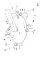
次に、上記基板洗浄装置201A、201B、202A、202Bとして用いられる、ロールタイプ若しくはペンシルタイプの基板洗浄装置の詳細な構成について説明する。これらの基板洗浄装置は、図3〜図6に示す基板保持回転機構1を共通して備えている。この基板保持回転機構1の上部に、ロールタイプの洗浄機構2A(図7参照)若しくはペンシルタイプの洗浄機構2B(図8参照)が設置されることで、各基板洗浄装置201A、201B、202A、202Bが構成される。
まず、基板保持回転機構1について説明する。図3に示すように、基板保持回転機構1の中央部には、洗浄機構2A若しくは洗浄機構2Bを駆動させる洗浄部材駆動機構30が設置されている。洗浄部材駆動機構30を挟む両側には、第1移動機構10および第2移動機構20が配置されている。第1移動機構10は第1スピンドル群G1を移動させ、第2移動機構20は第2スピンドル群G2を移動させる。第1スピンドル群G1は第1駆動スピンドル50Aおよびアイドラスピンドル50Bを含み、第2スピンドル群G2は複数の第2駆動スピンドル50Cを含む。
基板保持回転機構1は、各駆動ローラ52および従動ローラ54の保持溝52a、54aによって基板Wを保持しながら、駆動ローラ52の回転力によって、基板Wを回転させる。
図3に示すように、支柱部材33の上端には、後述する洗浄機構が取り付けられる取付部34が設けられている。一方、ケース31の両側には、該ケース31を挟んで互いに平行に配置された一対の直線状のスライドレール36が配設されている。この一対のスライドレール36の両端部に、第1移動機構10および第2移動機構20がスライド移動可能に取り付けられている。
ここで、第1移動機構10の構成を説明する。図3、4に示すように、各スライドレール36には、断面視で略U字状のスライダー12が係合されている。スライダー12は、スライドレール36が延びる方向に、このスライドレール36に対してスライド移動する。各スライダー12の下面には、略矩形の平板状に形成された連結部材13が取り付けられている。連結部材13の中央部には上下に貫通する開口部13aが設けられ、該開口部13aの内周にベアリング14が嵌合されている。ベアリング14の内輪14aには、略円柱状の軸部材15が取り付けられている。軸部材15は、開口部13a内で、ベアリング14によって連結部材13に対して回転可能に保持されている。開口部13aの上部には、開口部13a内に設置された軸部材15の上面を覆うカバー16が取り付けられている。
すなわち、第1移動機構10は、第1スピンドル群G1を、スライドレール36に沿ってスライド移動可能かつ、軸部材15回りに回転移動可能に保持している。
図3に示すように、各スピンドル50A、50Bにおける本体部51の上端部には、駆動ローラ52若しくは従動ローラ54(図7参照)を取り付ける取付部51aが設けられている。この取付部51aから突出するシャフト26の上端部26aが、駆動ローラ52若しくは従動ローラ54に接続されることで、シャフト26と駆動ローラ52若しくは従動ローラ54とが一体に回転する。なお図3では、駆動ローラ52および従動ローラ54を取付部51aから取り外した状態を示している。
以上のようにして、回転検出部53は、従動ローラ54の回転数を検出することで、基板Wの回転数を間接的に検出する。
第2移動機構20は、上記第1移動機構10が備えるベース部材17および連結部材13に代えて、これらの部材13、17を一体に構成したものに相当する一枚のベース部材25を備えている。また、第2移動機構20では、図示は省略するが、モータによって2本の第2駆動スピンドル50Cのシャフト26が同期して回転するように構成されている。第2移動機構20の、その他の部分の構成は、第1移動機構10と共通である。従って、第2移動機構20の図示およびその説明では、第1移動機構と共通する部分には同一の符号を付し、その詳細な説明は省略する。
すなわち、第2移動機構20は、第2スピンドル群G2をスライドレール36に沿う直線方向にスライド移動可能かつ回転移動不能に保持している。
次に、基板保持回転機構1の上部に取り付けられる、ロールタイプの洗浄機構2Aについて説明する。図7に示す洗浄機構2Aは、基板Wを洗浄するロール洗浄部材60と、基板Wの上面に向けて洗浄液を供給する上部ノズル71と、基板Wの下面に向けて洗浄液を供給する下部ノズル72と、を備えている。
次に、ペンシルタイプの洗浄機構2Bについて説明する。図8に示す洗浄機構2Bは、回転軸67と、揺動アーム68と、ペンシル型の洗浄部材69と、を備えている。揺動アーム68は、回転軸67回りに回転させられる。洗浄部材69は、揺動アーム68の先端部における下面に取り付けられている。洗浄部材69は、上下方向に延びる円柱状に形成されている。洗浄部材69の材質としては、発泡ポリウレタン、PVAなどを用いることができる。
基板Wを保持する際、図9(a)に示すように、スライド方向Lで基板Wを挟む両側に配置された第1スピンドル群G1および第2スピンドル群G2を、第1移動機構10および第2移動機構20によって、基板Wに向けて移動させる。このとき、第2スピンドル群G2が、第1スピンドル群G1よりも早く基板Wに接触する。第1スピンドル群G1および第2スピンドル群G2の両者が基板Wの周縁部に当接することで、基板Wが保持される。
さらに、従動ローラ54の基板Wへの押し付け力を、駆動ローラ52の基板への押し付け力と同等にしたとしても、基板Wに加えられる力のバランスが上記特許文献1の構成と比較して悪化しないため、基板Wの変形などを抑えながら、強い力で従動ローラ54を基板Wに押し付けて、従動ローラ54と基板Wとの間で生じるスリップを抑止することができる。
さらに、本実施形態の基板処理装置200によれば、研磨部103で研磨された基板Wを基板洗浄装置201A、201B、202A、202Bで洗浄する際に、基板Wの回転数を精度よく測定しつつ、駆動ローラ52や従動ローラ54の汚れが基板Wに再度付着することなどを抑えて、処理された基板Wの品質を安定させることができる。
Claims (7)
- 基板を回転させる第1駆動ローラを有する第1駆動スピンドルと、前記基板によって回転させられる従動ローラを有するアイドラスピンドルと、を含む第1スピンドル群と、
前記基板を回転させる第2駆動ローラをそれぞれ有する複数の第2駆動スピンドルを含む第2スピンドル群と、
前記第1駆動ローラおよび複数の前記第2駆動ローラによって回転させられる前記基板に洗浄部材を接触させて前記基板を洗浄する洗浄機構と、
前記従動ローラの回転数を検出する回転検出部と、
前記第1スピンドル群をスライド移動可能かつ回転移動可能に保持する第1移動機構と、
前記第2スピンドル群をスライド移動可能かつ回転移動不能に保持する第2移動機構と、を備え、
前記洗浄部材は、前記基板と接触している間において回転または揺動することで、前記基板を押し込む押し込み力を発生させ、
前記押し込み力は、前記基板を前記第1スピンドル群から前記第2スピンドル群に向けて押し込む方向に成分を有する、基板洗浄装置。 - 前記従動ローラを回転させる際の慣性モーメントが、前記第1駆動ローラを回転させる際の慣性モーメントよりも小さい、請求項1に記載の基板洗浄装置。
- 基板を回転させる第1駆動ローラおよび複数の第2駆動ローラと、
回転する前記基板に接触することで回転する従動ローラと、
回転する前記基板に洗浄部材を接触させて前記基板を洗浄する洗浄機構と、
前記従動ローラの回転数を検出する回転検出部と、
前記第1駆動ローラおよび前記従動ローラをスライド移動可能かつ回転移動可能に保持する第1移動機構と、
複数の前記第2駆動ローラをスライド移動可能かつ回転移動不能に保持する第2移動機構と、を備え、
前記洗浄部材は、前記基板と接触している間において回転または揺動することで、前記基板を押し込む押し込み力を発生させ、
前記押し込み力は、前記基板を、前記第1駆動ローラおよび前記従動ローラから前記複数の第2駆動ローラに向けて押し込む方向に成分を有し、
前記回転検出部は、前記従動ローラとともに回転するドグと、投光部および受光部を有するセンサと、を備え、前記投光部と前記受光部との間に前記ドグが位置するか否かによって変化する前記センサの出力信号に基づいて、前記ドグの回転数を検出するように構成されている、基板洗浄装置。 - 前記洗浄部材は、回転する前記基板と接触するロール洗浄部材であり、
前記ロール洗浄部材は前記基板との接触部において前記基板を複数の前記第2駆動ローラに向けて押し込む方向に回転するように構成されている、請求項1から請求項3のいずれか1項に記載の基板洗浄装置。 - 前記洗浄部材は、回転する前記基板と接触するペンシル洗浄部材であり、
前記洗浄機構は、該ペンシル洗浄部材が前記基板の中心と外周とを結ぶ所定の軌跡を揺動するように該ペンシル洗浄部材が取り付けられた揺動アームを有し、
前記揺動アームは、前記ペンシル洗浄部材が前記基板と接触している間において、前記第1駆動ローラおよび前記従動ローラから複数の前記第2駆動ローラに向かう方向に揺動する、請求項1から請求項3のいずれか1項に記載の基板洗浄装置。 - 第1洗浄室、第1搬送室、第2洗浄室、第2搬送室及び乾燥室を有する洗浄部を備えた基板処理装置であって、
前記第1洗浄室及び前記第2洗浄室はそれぞれ、請求項1から請求項5のいずれか1項に記載の基板洗浄装置を含む、基板処理装置。 - 前記基板を研磨する研磨部と、
請求項1から請求項5のいずれか1項に記載の基板洗浄装置を有する洗浄部と、を備える基板処理装置。
Priority Applications (7)
| Application Number | Priority Date | Filing Date | Title |
|---|---|---|---|
| JP2017097621A JP6792512B2 (ja) | 2017-05-16 | 2017-05-16 | 基板洗浄装置および基板処理装置 |
| KR1020180052454A KR102494451B1 (ko) | 2017-05-16 | 2018-05-08 | 기판 세정 장치, 기판 처리 장치, 및 기판 세정 방법 |
| CN201810450204.3A CN108878314B (zh) | 2017-05-16 | 2018-05-11 | 基板清洗装置及基板处理装置 |
| TW107116219A TWI770175B (zh) | 2017-05-16 | 2018-05-14 | 基板清洗裝置及基板處理裝置 |
| SG10201804063YA SG10201804063YA (en) | 2017-05-16 | 2018-05-14 | Substrate cleaning apparatus, substrate processing apparatus, and method of cleaning substrate |
| US15/978,320 US10741423B2 (en) | 2017-05-16 | 2018-05-14 | Substrate cleaning apparatus, substrate processing apparatus, and method of cleaning substrate |
| US16/919,788 US11532491B2 (en) | 2017-05-16 | 2020-07-02 | Substrate cleaning apparatus, substrate processing apparatus, and method of cleaning substrate |
Applications Claiming Priority (1)
| Application Number | Priority Date | Filing Date | Title |
|---|---|---|---|
| JP2017097621A JP6792512B2 (ja) | 2017-05-16 | 2017-05-16 | 基板洗浄装置および基板処理装置 |
Publications (3)
| Publication Number | Publication Date |
|---|---|
| JP2018195680A JP2018195680A (ja) | 2018-12-06 |
| JP2018195680A5 JP2018195680A5 (ja) | 2019-12-12 |
| JP6792512B2 true JP6792512B2 (ja) | 2020-11-25 |
Family
ID=64272527
Family Applications (1)
| Application Number | Title | Priority Date | Filing Date |
|---|---|---|---|
| JP2017097621A Active JP6792512B2 (ja) | 2017-05-16 | 2017-05-16 | 基板洗浄装置および基板処理装置 |
Country Status (6)
| Country | Link |
|---|---|
| US (2) | US10741423B2 (ja) |
| JP (1) | JP6792512B2 (ja) |
| KR (1) | KR102494451B1 (ja) |
| CN (1) | CN108878314B (ja) |
| SG (1) | SG10201804063YA (ja) |
| TW (1) | TWI770175B (ja) |
Families Citing this family (10)
| Publication number | Priority date | Publication date | Assignee | Title |
|---|---|---|---|---|
| JP6792512B2 (ja) * | 2017-05-16 | 2020-11-25 | 株式会社荏原製作所 | 基板洗浄装置および基板処理装置 |
| JP7356811B2 (ja) * | 2019-04-02 | 2023-10-05 | 株式会社荏原製作所 | 基板支持装置及び基板支持装置の制御方法 |
| CN110148573B (zh) * | 2019-04-17 | 2020-12-04 | 湖州达立智能设备制造有限公司 | 一种半导体设备工艺腔的晶圆升降装置 |
| KR102428923B1 (ko) * | 2020-01-22 | 2022-08-04 | 주식회사 씨티에스 | 씨엠피 장치 |
| KR20220036517A (ko) * | 2020-09-16 | 2022-03-23 | 삼성전자주식회사 | 웨이퍼 클리닝 장치 및 이를 이용한 웨이퍼 클리닝 방법 |
| KR102590328B1 (ko) * | 2020-12-24 | 2023-10-16 | 세메스 주식회사 | 기판 파지 장치 및 이를 포함하는 액 처리 장치, 및 기판 처리 설비 |
| CN112820627B (zh) * | 2020-12-30 | 2022-10-18 | 江苏亚电科技有限公司 | 一种高效晶圆片的清洗方法 |
| CN113607980B (zh) * | 2021-10-08 | 2021-11-30 | 南通优睿半导体有限公司 | 一种半导体器材料研发的选择测试装置 |
| CN113621786B (zh) * | 2021-10-13 | 2021-12-14 | 南通锦发电缆有限公司 | 一种用于电线电缆制造的退火装置 |
| KR20230140641A (ko) * | 2022-03-29 | 2023-10-10 | 삼성디스플레이 주식회사 | 임프린트 장치 |
Family Cites Families (19)
| Publication number | Priority date | Publication date | Assignee | Title |
|---|---|---|---|---|
| JP2582976B2 (ja) * | 1991-12-19 | 1997-02-19 | 大日本スクリーン製造株式会社 | 回転式基板処理装置における基板の有無検出装置 |
| JPH10289889A (ja) | 1997-04-16 | 1998-10-27 | Dainippon Screen Mfg Co Ltd | 基板処理装置 |
| JP3964517B2 (ja) * | 1997-10-31 | 2007-08-22 | 芝浦メカトロニクス株式会社 | 洗浄装置とその方法 |
| JP3343503B2 (ja) * | 1997-12-12 | 2002-11-11 | 東京エレクトロン株式会社 | 洗浄装置 |
| JP2001038614A (ja) * | 1999-07-26 | 2001-02-13 | Ebara Corp | 研磨装置 |
| US7685667B2 (en) * | 2005-06-14 | 2010-03-30 | Taiwan Semiconductor Manufacturing Co., Ltd. | Post-CMP cleaning system |
| US7938130B2 (en) * | 2006-03-31 | 2011-05-10 | Ebara Corporation | Substrate holding rotating mechanism, and substrate processing apparatus |
| JP4937807B2 (ja) * | 2006-03-31 | 2012-05-23 | 株式会社荏原製作所 | 基板保持回転機構、基板処理装置 |
| US20080011325A1 (en) * | 2006-06-05 | 2008-01-17 | Olgado Donald J | Methods and apparatus for supporting a substrate in a horizontal orientation during cleaning |
| KR100786627B1 (ko) | 2006-07-24 | 2007-12-21 | 두산메카텍 주식회사 | 웨이퍼의 회전 감지장치 |
| US7823241B2 (en) | 2007-03-22 | 2010-11-02 | Taiwan Semiconductor Manufacturing Co., Ltd. | System for cleaning a wafer |
| JP2010169606A (ja) * | 2009-01-26 | 2010-08-05 | Mitsuboshi Belting Ltd | 動力伝達機構の耐久試験機 |
| JP2015220402A (ja) * | 2014-05-20 | 2015-12-07 | 株式会社荏原製作所 | 基板洗浄装置および基板洗浄装置で実行される方法 |
| JP6178019B2 (ja) * | 2014-10-31 | 2017-08-09 | 株式会社荏原製作所 | 基板洗浄装置及び基板洗浄方法 |
| SG10201601095UA (en) | 2015-02-18 | 2016-09-29 | Ebara Corp | Substrate cleaning apparatus, substrate cleaning method, and substrate processing apparatus |
| JP6491908B2 (ja) * | 2015-03-09 | 2019-03-27 | 株式会社荏原製作所 | 基板洗浄装置、基板洗浄方法、および基板処理装置 |
| JP6491903B2 (ja) * | 2015-02-19 | 2019-03-27 | 株式会社荏原製作所 | 基板洗浄装置および方法 |
| JP6328577B2 (ja) * | 2015-02-24 | 2018-05-23 | 株式会社荏原製作所 | 荷重測定装置および荷重測定方法 |
| JP6792512B2 (ja) * | 2017-05-16 | 2020-11-25 | 株式会社荏原製作所 | 基板洗浄装置および基板処理装置 |
-
2017
- 2017-05-16 JP JP2017097621A patent/JP6792512B2/ja active Active
-
2018
- 2018-05-08 KR KR1020180052454A patent/KR102494451B1/ko active IP Right Grant
- 2018-05-11 CN CN201810450204.3A patent/CN108878314B/zh active Active
- 2018-05-14 SG SG10201804063YA patent/SG10201804063YA/en unknown
- 2018-05-14 US US15/978,320 patent/US10741423B2/en active Active
- 2018-05-14 TW TW107116219A patent/TWI770175B/zh active
-
2020
- 2020-07-02 US US16/919,788 patent/US11532491B2/en active Active
Also Published As
| Publication number | Publication date |
|---|---|
| US11532491B2 (en) | 2022-12-20 |
| TW201902585A (zh) | 2019-01-16 |
| US20200335363A1 (en) | 2020-10-22 |
| JP2018195680A (ja) | 2018-12-06 |
| TWI770175B (zh) | 2022-07-11 |
| KR102494451B1 (ko) | 2023-02-01 |
| SG10201804063YA (en) | 2018-12-28 |
| KR20180125887A (ko) | 2018-11-26 |
| CN108878314B (zh) | 2023-09-29 |
| US10741423B2 (en) | 2020-08-11 |
| US20180337072A1 (en) | 2018-11-22 |
| CN108878314A (zh) | 2018-11-23 |
Similar Documents
| Publication | Publication Date | Title |
|---|---|---|
| JP6792512B2 (ja) | 基板洗浄装置および基板処理装置 | |
| KR102263992B1 (ko) | 기판 처리 장치 및 처리 방법 | |
| JP4763755B2 (ja) | ポリッシング装置 | |
| KR20210030331A (ko) | 기판 처리 장치 | |
| JP5188952B2 (ja) | 基板処理装置 | |
| US9144881B2 (en) | Polishing apparatus and polishing method | |
| US8087419B2 (en) | Substrate holding rotating mechanism, and substrate processing apparatus | |
| KR20160030855A (ko) | 처리 모듈, 처리 장치 및 처리 방법 | |
| CN105164793B (zh) | 对于利用用于化学机械抛光的晶片及晶片边缘/斜角清洁模块的盘/垫清洁的设计 | |
| JP6710129B2 (ja) | 基板洗浄装置および基板洗浄方法 | |
| TWI433754B (zh) | 研磨裝置 | |
| KR102307209B1 (ko) | 버프 처리 장치 및 기판 처리 장치 | |
| JP7165104B2 (ja) | 洗浄部材の着脱用治具 | |
| JP2008132592A (ja) | ポリッシング装置およびポリッシング方法 | |
| JP6426965B2 (ja) | 処理コンポーネント、処理モジュール、及び、処理方法 | |
| WO2023037716A1 (ja) | 基板洗浄装置、基板処理装置、及び基板洗浄装置のメンテナンス方法 | |
| JP6353266B2 (ja) | 冷却装置、及び、基板処理装置 | |
| KR20240052946A (ko) | 기판 세정 장치, 기판 처리 장치, 및 기판 세정 장치의 메인터넌스 방법 | |
| JP6412385B2 (ja) | コンディショニング部、バフ処理モジュール、基板処理装置、及び、ドレスリンス方法 | |
| JP2022124016A (ja) | 基板洗浄装置、基板洗浄装置の異常判定方法、基板洗浄装置の異常判定プログラム |
Legal Events
| Date | Code | Title | Description |
|---|---|---|---|
| A521 | Request for written amendment filed |
Free format text: JAPANESE INTERMEDIATE CODE: A523 Effective date: 20191029 |
|
| A621 | Written request for application examination |
Free format text: JAPANESE INTERMEDIATE CODE: A621 Effective date: 20191029 |
|
| A977 | Report on retrieval |
Free format text: JAPANESE INTERMEDIATE CODE: A971007 Effective date: 20200722 |
|
| A131 | Notification of reasons for refusal |
Free format text: JAPANESE INTERMEDIATE CODE: A131 Effective date: 20200818 |
|
| A521 | Request for written amendment filed |
Free format text: JAPANESE INTERMEDIATE CODE: A523 Effective date: 20201006 |
|
| TRDD | Decision of grant or rejection written | ||
| A01 | Written decision to grant a patent or to grant a registration (utility model) |
Free format text: JAPANESE INTERMEDIATE CODE: A01 Effective date: 20201027 |
|
| A61 | First payment of annual fees (during grant procedure) |
Free format text: JAPANESE INTERMEDIATE CODE: A61 Effective date: 20201106 |
|
| R150 | Certificate of patent or registration of utility model |
Ref document number: 6792512 Country of ref document: JP Free format text: JAPANESE INTERMEDIATE CODE: R150 |
|
| R250 | Receipt of annual fees |
Free format text: JAPANESE INTERMEDIATE CODE: R250 |