以下、本発明の実施の形態について図面を参照しながら説明する。但し、本発明の構成は多くの異なる態様で実施することが可能であり、本発明の趣旨及びその範囲から逸脱することなくその形態及び詳細を様々に変更し得ることは当業者であれば容易に理解される。したがって本実施の形態の記載内容に限定して解釈されるものではない。
なお、各実施の形態の図面等において示す各構成の、大きさ、層の厚さ、または領域は、明瞭化のために誇張されて表記している場合がある。よって、必ずしもそのスケールに限定されない。
なお本明細書にて用いる第1、第2、第3、乃至第N(Nは自然数)という用語は、構成要素の混同を避けるために付したものであり、数的に限定するものではないことを付記する。
(実施の形態1)
本実施の形態では、開示する発明の一態様にかかる半導体装置及び半導体装置の作製方法について、図1乃至図4を用いて説明する。
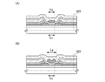
図1は、半導体装置の構成の一例であるトランジスタ420の断面図である。なおトランジスタ420はチャネル形成領域が1つ形成されるシングルゲート構造を示すが、チャネル形成領域が2つ形成されるダブルゲート構造もしくは3つ形成されるトリプルゲート構造であってもよい。
トランジスタ420は、絶縁表面を有する基板400上に、バッファ層436と、酸化物半導体層403と、第1の導電層405a、405bと、第2の導電層465a、465bと、絶縁層407と、ゲート絶縁層402と、ゲート電極層401と、層間絶縁層408と、を有する(図1参照)。
本実施の形態で開示する図1の構造は、トランジスタ420のソース電極及びドレイン電極として機能する第1の導電層405a、405bを、酸化物半導体層403と重畳する領域において、ゲート絶縁層402を介してゲート電極層401と重畳させる。また本実施の形態で開示する図1の構造は、トランジスタ420のソース電極及びドレイン電極として機能する第2の導電層465a、465bを、酸化物半導体層403と重畳する領域において、ゲート絶縁層402を介してゲート電極層401と重畳させない。
本実施の形態で開示する図1の構造は、トランジスタ420のソース電極及びドレイン電極となる第1の導電層405a、405bの端部と、ゲート電極となるゲート電極層401の端部とを重畳して設けることができる。そのため、トランジスタのオン特性(例えば、オン電流や電界効果移動度)を向上させて、半導体装置の高速応答、高速駆動を実現することができる。
また本実施の形態で開示する図1の構造は、トランジスタのソース電極及びドレイン電極となる第1の導電層405a、405bを薄膜化することができる。第1の導電層405a、405bを薄膜化することで、特に酸化物半導体層403のチャネル形成領域周辺での、ゲート絶縁層402を形成する際の表面の段差を小さくすることができる。従って、ゲート絶縁層402は、カバレッジを良好にして形成することができる。カバレッジ不良を低減することで、電極間の短絡の発生を抑制し、信頼性の向上を図ることができる。加えて、本実施の形態で開示する図1の構造は、トランジスタのソース電極及びドレイン電極となる第2の導電層465a、465bの端部と、ゲート電極となるゲート電極層401の端部とを重畳させないで設けることができる。そのため、第1の導電層405a、405bに比べて第2の導電層465a、465bを厚膜化しても、電極間の短絡がない。したがって、第2の導電層465a、465bを厚膜化することで、電極間での短絡を引き起こすことなく、ソース電極及びドレイン電極を流れる電流を大きくすることができる。
また本実施の形態で開示する図1の構造は、第1の導電層405a、405bを薄膜化することで、エッチング等の工程により第1の導電層405a、405bを加工する際の所要期間を短くすることができる。そのため第1の導電層405a、405bをエッチング等の工程で加工する際に生じる、酸化物半導体層403へのダメージを低減することができる。そのため、信頼性の向上を図ることができる。
また本実施の形態で開示する図1の構造は、ゲート絶縁層402を薄膜化したコプレナー構造とすることができ、平坦性を高めたバッファ層436上に、酸化物半導体層403を薄膜化して形成することができる。ゲート絶縁層402及び酸化物半導体層403を薄膜化することで、オン特性の向上が図れるとともに、トランジスタを完全空乏型で動作させることも可能である。トランジスタを完全空乏型で動作させることで、高集積化、高速駆動化、低消費電力化を図ることができる。
また、本実施の形態で開示する図1の構造は、第2の導電層465a、465bと絶縁層407とを重畳して設け、側面をエッチング等の加工によりテーパー状とすることができる。そのため第2の導電層465a、465bを厚膜化しても、カバレッジを良好にすることができる。
以上説明したように、本実施の形態で開示する図1の構成では、トランジスタのソース電極及びドレイン電極を流れる電流を低減させることなく、トランジスタのソース電極及びドレイン電極と、ゲート電極とを重畳して設けることができ、オン特性を向上させることができる。さらに本実施の形態で開示する図1の構成では、ゲート絶縁層のカバレッジ不良を低減することで、酸化物半導体層及びゲート絶縁層を薄膜化することができる。この場合、酸化物半導体をチャネル形成領域に設けるトランジスタを微細化して形成することができ好適である。
次いで、図2(A)乃至(E)に、図1で示したトランジスタ420の作製方法の一例を示す。
まず、絶縁表面を有する基板400上にバッファ層436を形成する。バッファ層436は、バッファ層436上に形成される酸化物半導体層403と絶縁表面を有する基板400との反応を抑制するための層である。
絶縁表面を有する基板400に使用することができる基板に大きな制限はないが、少なくとも、後の熱処理に耐えうる程度の耐熱性を有していることが必要となる。例えば、バリウムホウケイ酸ガラスやアルミノホウケイ酸ガラスなどのガラス基板、セラミック基板、石英基板、サファイア基板などを用いることができる。また、シリコンや炭化シリコンなどの単結晶半導体基板、多結晶半導体基板、シリコンゲルマニウムなどの化合物半導体基板、SOI基板などを適用することもでき、これらの基板上に半導体素子が設けられたものを、基板400として用いてもよい。
バッファ層436は、酸化物半導体層403と接する層であるため、酸化物半導体層403と同種の成分でなる酸化物を用いるのが好ましい。具体的には、アルミニウム(Al)、ガリウム(Ga)、ジルコニウム(Zr)、ハフニウム(Hf)等の酸化物半導体層403の構成元素、または、アルミニウム、ガリウム等と同族の元素である希土類元素、から選択された一以上の元素の酸化物を含む層とするのが好ましい。また、これらの元素のうち、III族元素であるアルミニウム、ガリウム、または希土類元素の酸化物を用いるのがより好ましい。また、希土類元素としてはスカンジウム(Sc)、イットリウム(Y)、セリウム(Ce)、サマリウム(Sm)またはガドリニウム(Gd)を用いるのが好ましい。このような材料は、酸化物半導体層403と相性がよく、これをバッファ層436に用いることで、酸化物半導体層403との界面の状態を良好にすることができる。また、酸化物半導体層403の結晶性を向上させることができる。
なお、酸化物半導体層403をトランジスタ420の活性層として用いるため、バッファ層436のエネルギーギャップは酸化物半導体層403よりも大きいことが求められ、バッファ層436は絶縁性を有するのが好ましい。
バッファ層436は、単層でも積層でもよい。
バッファ層436の作製方法としては特に限定はなく、プラズマCVD法又はスパッタリング法等を用いて形成することができる。
バッファ層436の表面は、平坦化処理を行ってもよい。平坦化処理としては、特に限定されないが、研磨処理(例えば、化学的機械研磨(Chemical Mechanical Polishing:CMP)法)、ドライエッチング処理、プラズマ処理を用いることができる。
次に、バッファ層436上に酸化物半導体層403を形成する。
酸化物半導体層403を形成する際、できる限り酸化物半導体層403に含まれる水素濃度を低減させることが好ましい。水素濃度を低減させるには、例えば、スパッタリング法を用いて成膜を行う場合には、スパッタリング装置の処理室内に供給する雰囲気ガスとして、水素、水、水酸基または水素化物などの不純物が除去された高純度の希ガス(代表的にはアルゴン)、酸素、および希ガスと酸素との混合ガスを適宜用いる。
また、酸化物半導体層403、バッファ層436を大気に解放せずに連続的に形成することが好ましい。酸化物半導体層403、バッファ層436を大気に曝露せずに連続して形成すると、これらの界面に水素や水分などの不純物が吸着することを防止することができる。
また、基板400を高温に保持した状態で酸化物半導体層403を形成することも、酸化物半導体層403中に含まれうる不純物濃度を低減するのに有効である。基板400を加熱する温度としては、150℃以上450℃以下とすればよく、好ましくは基板温度が200℃以上350℃以下とすればよい。また、酸化物半導体層403の形成時に基板400を高温で加熱することで、結晶性を有する酸化物半導体層を形成することができる。
酸化物半導体層403に用いる酸化物半導体としては、少なくともインジウム(In)あるいは亜鉛(Zn)を含むことが好ましい。特にInとZnを含むことが好ましい。また、該酸化物半導体を用いたトランジスタの電気特性のばらつきを減らすためのスタビライザーとして、それらに加えてガリウム(Ga)を有することが好ましい。また、スタビライザーとしてスズ(Sn)を有することが好ましい。また、スタビライザーとしてハフニウム(Hf)を有することが好ましい。また、スタビライザーとしてアルミニウム(Al)を有することが好ましい。また、スタビライザーとしてジルコニウム(Zr)を有することが好ましい。
また、他のスタビライザーとして、ランタノイドである、ランタン(La)、セリウム(Ce)、プラセオジム(Pr)、ネオジム(Nd)、サマリウム(Sm)、ユウロピウム(Eu)、ガドリニウム(Gd)、テルビウム(Tb)、ジスプロシウム(Dy)、ホルミウム(Ho)、エルビウム(Er)、ツリウム(Tm)、イッテルビウム(Yb)、ルテチウム(Lu)のいずれか一種あるいは複数種を有してもよい。
例えば、酸化物半導体として、酸化インジウム、酸化スズ、酸化亜鉛、二元系金属の酸化物であるIn−Zn系酸化物、Sn−Zn系酸化物、Al−Zn系酸化物、Zn−Mg系酸化物、Sn−Mg系酸化物、In−Mg系酸化物、In−Ga系酸化物、三元系金属の酸化物であるIn−Ga−Zn系酸化物(IGZOとも表記する)、In−Al−Zn系酸化物、In−Sn−Zn系酸化物、Sn−Ga−Zn系酸化物、Al−Ga−Zn系酸化物、Sn−Al−Zn系酸化物、In−Hf−Zn系酸化物、In−La−Zn系酸化物、In−Ce−Zn系酸化物、In−Pr−Zn系酸化物、In−Nd−Zn系酸化物、In−Sm−Zn系酸化物、In−Eu−Zn系酸化物、In−Gd−Zn系酸化物、In−Tb−Zn系酸化物、In−Dy−Zn系酸化物、In−Ho−Zn系酸化物、In−Er−Zn系酸化物、In−Tm−Zn系酸化物、In−Yb−Zn系酸化物、In−Lu−Zn系酸化物、四元系金属の酸化物であるIn−Sn−Ga−Zn系酸化物、In−Hf−Ga−Zn系酸化物、In−Al−Ga−Zn系酸化物、In−Sn−Al−Zn系酸化物、In−Sn−Hf−Zn系酸化物、In−Hf−Al−Zn系酸化物を用いることができる。
なお、ここで、例えば、In−Ga−Zn系酸化物とは、InとGaとZnを有する酸化物という意味であり、InとGaとZnの比率は問わない。また、InとGaとZn以外の金属元素が入っていてもよい。
なお、酸化物半導体層403は、形成時に酸素が多く含まれるような条件(例えば、酸素100%の雰囲気下でスパッタリング法で形成するなど)で形成し、酸素を多く含む(好ましくは酸化物半導体が結晶状態における化学量論的組成に対し、酸素の含有量が過剰な領域が含まれている)ことが好ましい。
また酸化物半導体層403の形成時に用いるスパッタリングガスは水素、水、水酸基又は水素化物などの不純物が除去された高純度ガスを用いることが好ましい。
なお、電子供与体(ドナー)となる水分または水素などの不純物が低減され、なおかつ酸素欠損が低減されることにより高純度化された酸化物半導体(purified Oxide Semiconductor)は、i型(真性半導体)又はi型に限りなく近い。そのため、上記酸化物半導体を用いたトランジスタは、オフ電流が著しく低いという特性を有する。また、酸化物半導体のバンドギャップは、2eV以上、好ましくは2.5eV以上、より好ましくは3eV以上である。水分または水素などの不純物濃度が十分に低減され、なおかつ酸素欠損が低減されることにより高純度化された酸化物半導体層を用いることにより、トランジスタのオフ電流を下げることができる。
なお、特に断りがない限り、本明細書でオフ電流とは、nチャネル型トランジスタにおいては、ドレイン端子をソース端子とゲートよりも高い電位とした状態において、ソース端子の電位を基準としたときのゲートの電位が0以下であるときに、ソース端子とドレイン端子の間に流れる電流のことを意味する。
なお酸化物半導体は、単結晶、多結晶(ポリクリスタルともいう。)または非晶質などの状態を採ることができる。特に酸化物半導体層403として用いる酸化物半導体は、結晶領域及びアモルファス領域を含む混合層であり、結晶性を有する酸化物半導体とすることが好ましい。
結晶性を有する酸化物半導体では、よりバルク内欠陥を低減することができ、表面の平坦性を高めればより高い移動度を得ることができる。表面の平坦性を高めるためには、平坦な表面上に酸化物半導体を形成することが好ましく、具体的には、平均面粗さ(Ra)が1nm以下、好ましくは0.3nm以下、より好ましくは0.1nm以下の表面上に形成するとよい。
なお、Raは、JIS B 0601:2001(ISO4287:1997)で定義されている算術平均粗さを曲面に対して適用できるよう三次元に拡張したものであり、「基準面から指定面までの偏差の絶対値を平均した値」と表現でき、以下の式にて定義される。
ここで、指定面とは、粗さ計測の対象となる面であり、座標((x1,y1,f(x1,y1))(x1,y2,f(x1,y2))(x2,y1,f(x2,y1))(x2,y2,f(x2,y2))の4点で表される四角形の領域とし、指定面をxy平面に投影した長方形の面積をS0、基準面の高さ(指定面の平均の高さ)をZ0とする。Raは原子間力顕微鏡(AFM:Atomic Force Microscope)にて評価可能である。
結晶性を有する酸化物半導体は、好ましくは、CAAC−OS(C Axis Aligned Crystalline Oxide Semiconductor)とする。
CAAC−OSは、完全な単結晶ではなく、完全な非晶質でもない。CAAC−OSは、非晶質相に数nmから数十nmの結晶部及び非晶質を有する結晶−非晶質混相構造の酸化物半導体である。なお、透過型電子顕微鏡(TEM:Transmission Electron Microscope)によるCAAC−OSに含まれる非晶質部と結晶部との境界は明確ではない。また、CAAC−OSには粒界(グレインバウンダリーともいう。)は確認できない。CAAC−OSが粒界を有さないため、粒界に起因する電子移動度の低下が起こりにくい。
CAAC−OSに含まれる結晶部は、c軸がCAAC−OSの被形成面または表面に垂直な方向に揃い、かつab面に垂直な方向から見て三角形状または六角形状の原子配列を有し、c軸に垂直な方向から見て金属原子が層状または金属原子と酸素原子とが層状に配列している。なお、結晶部同士は、それぞれa軸およびb軸の向きが異なっていてもよい。
なお、CAAC−OS中の、非晶質部および結晶部の占める割合が均一でなくてもよい。例えば、CAAC−OSの表面側から結晶成長させる場合、CAAC−OSの表面の近傍は結晶部の占める割合が高くなり、被形成面の近傍は非晶質部の占める割合が高くなることがある。
CAAC−OSに含まれる結晶部のc軸は、CAAC−OSの被形成面または表面に垂直な方向に揃うため、CAAC−OS形状(被形成面の断面形状または表面の断面形状)によって、結晶部同士のc軸の方向が異なることがある。なお、結晶部のc軸の方向は、CAAC−OSが形成されたときの被形成面または表面に垂直な方向となる。結晶部は、成膜後または成膜後に加熱処理などの結晶化処理を行うことで形成される。
CAAC−OSを用いることで、可視光や紫外光の照射によるトランジスタの電気特性の変動が低減されるため、信頼性の高いトランジスタを得ることができる。
上述した酸化物半導体層403の一例としては、In(インジウム)、Ga(ガリウム)、及びZn(亜鉛)を含むターゲットを用いたスパッタリング法で形成したIn−Ga−Zn系酸化物があげられる。酸化物半導体層403は、1nm以上30nm以下(好ましくは5nm以上20nm以下)として形成することができる。
なおCAAC−OSを成膜する場合は、例えば、多結晶である酸化物半導体スパッタリング用ターゲットを用い、スパッタリング法によって成膜する。当該スパッタリング用ターゲットにイオンが衝突すると、スパッタリング用ターゲットに含まれる結晶領域がa−b面から劈開し、a−b面に平行な面を有する平板状またはペレット状のスパッタリング粒子として剥離することがある。この場合、当該平板状のスパッタリング粒子が、結晶状態を維持したまま基板に到達することで、CAAC−OSを成膜することができる。
In−Ga−Zn系酸化物をスパッタリング法で形成する場合、好ましくは、原子数比がIn:Ga:Zn=1:1:1、4:2:3、3:1:2、1:1:2、2:1:3、または3:1:4で示されるIn−Ga−Zn系酸化物のターゲットを用いる。前述の原子数比を有するIn−Ga−Zn系酸化物のターゲットを用いて酸化物半導体層を形成することで、多結晶またはCAAC−OSが形成されやすくなる。また、In、Ga、及びZnを含むターゲットの充填率は90%以上100%以下、好ましくは95%以上100%未満である。充填率の高いターゲットを用いることにより、形成した酸化物半導体層は緻密な層となる。
そして酸化物半導体層は、減圧状態に保持された処理室内に基板を保持し、処理室内の残留水分を除去しつつ水素及び水分が除去されたスパッタガスを導入し、上記ターゲットを用いて形成すればよい。形成時に、基板温度を100℃以上600℃以下、好ましくは200℃以上400℃以下としても良い。基板を加熱しながら形成することにより、形成した酸化物半導体層に含まれる不純物濃度を低減することができる。また、スパッタリングによる損傷が軽減される。処理室内の残留水分を除去するためには、吸着型の真空ポンプを用いることが好ましい。例えば、クライオポンプ、イオンポンプ、チタンサブリメーションポンプを用いることが好ましい。また、排気手段としては、ターボポンプにコールドトラップを加えたものであってもよい。クライオポンプを用いて形成室を排気すると、例えば、水素原子、水(H2O)など水素原子を含む化合物(より好ましくは炭素原子を含む化合物も)等が排気されるため、当該処理室で形成した酸化物半導体層に含まれる不純物の濃度を低減できる。
なお、スパッタリング法等で形成された酸化物半導体層中には、不純物としての水分または水素(水酸基を含む)が多量に含まれていることがある。そのため酸化物半導体層中の水分または水素などの不純物を低減(脱水化または脱水素化)するために、酸化物半導体層に対して、減圧雰囲気下、窒素や希ガスなどの不活性ガス雰囲気下、酸素ガス雰囲気下、または超乾燥エア(CRDS(キャビティリングダウンレーザー分光法)方式の露点計を用いて測定した場合の水分量が20ppm(露点換算で−55℃)以下、好ましくは1ppm以下、好ましくは10ppb以下の空気)雰囲気下で、加熱処理を施す。
酸化物半導体層に加熱処理を施すことで、酸化物半導体層中の水分または水素を脱離させることができる。具体的には、250℃以上750℃以下、好ましくは400℃以上基板の歪み点未満の温度で加熱処理を行えば良い。例えば、500℃、3分間以上6分間以下程度で行えばよい。加熱処理にRTA法を用いれば、短時間に脱水化または脱水素化が行えるため、ガラス基板の歪点を超える温度でも処理することができる。
なお、酸化物半導体層中の水分または水素を脱離させるための熱処理は、酸化物半導体層403の形成後であって後に形成する層間絶縁層408の形成前であれば、トランジスタ420の作製工程においてどのタイミングで行ってもよい。また、脱水化又は脱水素化のための熱処理は、複数回行ってもよく、他の加熱処理と兼ねてもよい。
また、上記加熱処理により、酸化物半導体層から酸素が脱離し、酸化物半導体層内に酸素欠損が形成される場合がある。よって、後の工程で酸化物半導体層と接するゲート絶縁層として、酸素を含むゲート絶縁層を用いることが好ましい。そして、酸素を含むゲート絶縁層を形成した後、加熱処理を施すことで、上記ゲート絶縁層から酸化物半導体層に酸素が供与されるようにする。上記構成により、ドナーとなる酸素欠損を低減し、酸化物半導体層に含まれる酸化物半導体の、化学量論的組成を満たすことができる。その結果、酸化物半導体層をi型に近づけることができ、酸素欠損によるトランジスタの電気的特性のばらつきを軽減し、電気的特性の向上を実現することができる。
なお、酸素を酸化物半導体層に供与するための加熱処理は、窒素、超乾燥空気、または希ガス(アルゴン、ヘリウムなど)の雰囲気下において、好ましくは200℃以上400℃以下、例えば250℃以上350℃以下で行う。上記ガスは、水の含有量が20ppm以下、好ましくは1ppm以下、より好ましくは10ppb以下であることが望ましい。
また、脱水化又は脱水素化処理を行った酸化物半導体層に、酸素(少なくとも、酸素ラジカル、酸素原子、酸素イオン、のいずれかを含む)を導入して層内に酸素を供給してもよい。
脱水化又は脱水素化処理を行った酸化物半導体層403に、酸素を導入して層内に酸素を導入することによって、酸化物半導体層403を高純度化、及びi型化することができる。高純度化し、i型化した酸化物半導体層403を有するトランジスタは、電気特性変動が抑制されており、電気的に安定である。
酸素の導入方法としては、イオン注入法、イオンドーピング法、プラズマイマージョンイオンインプランテーション法、プラズマ処理などを用いることができる。
酸化物半導体層403は、層状の酸化物半導体層をフォトリソグラフィ工程により島状の酸化物半導体層403に加工して形成することができる。
なお、酸化物半導体層403のエッチングは、ドライエッチングでもウェットエッチングでもよく、両方を用いてもよい。例えば、酸化物半導体層403のウェットエッチングに用いるエッチング液としては、燐酸と酢酸と硝酸を混ぜた溶液などを用いることができる。また、ITO07N(関東化学社製)を用いてもよい。
なお図2(A)では、島上の酸化物半導体層403は端部に20度乃至50度のテーパーを有している。端部が垂直であると酸素が抜けやすく酸素欠陥を生じやすいが、端部にテーパーを有することで酸素欠陥を抑制することができる。該酸素欠陥の抑制により、トランジスタ420のリーク電流(寄生チャネル)の発生を低減することができる。
次いで、酸化物半導体層403上及びバッファ層436上に、ソース電極層及びドレイン電極層(これと同じ層で形成される配線を含む)となる第1の導電層405を形成する。
該第1の導電層405は後の加熱処理に耐えられる材料を用いる。ソース電極層、及びドレイン電極層に用いる第1の導電層405としては、例えば、Al、Cr、Cu、Ta、Ti、Mo、Wから選ばれた元素を含む金属膜、又は上述した元素を成分とする金属窒化物膜(窒化チタン膜、窒化モリブデン膜、窒化タングステン膜)等を用いることができる。
なお、Al、Cuなどの金属膜を第1の導電層405として用いる場合には、該金属膜の下側又は上側の一方又は双方にTi、Mo、Wなどの高融点金属膜又はそれらの金属窒化物膜(窒化チタン膜、窒化モリブデン膜、窒化タングステン膜)を積層させた構成とすることが好ましい。
また、ソース電極層、及びドレイン電極層に用いる第1の導電層405としては、導電性の金属酸化物で形成しても良い。導電性の金属酸化物としては酸化インジウム(In2O3)、酸化スズ(SnO2)、酸化亜鉛(ZnO)、酸化インジウム酸化スズ(In2O3―SnO2、ITOと略記する)、酸化インジウム酸化亜鉛(In2O3―ZnO)又はこれらの金属酸化物材料に酸化シリコンを含ませたものを用いることができる。
上述した第1の導電層405は、後に形成する第2の導電層465よりも薄膜化しておくことが好ましい。具体的には、後に形成するゲート絶縁層402がカバレッジ不良を起こさない程度に薄膜化しておくことが好ましく、1nm以上30nm以下(好ましくは10nm以上20nm以下)として形成すればよい。
次いで、第1の導電層405上に、ソース電極層及びドレイン電極層(これと同じ層で形成される配線を含む)となる第2の導電層465を形成する。
該第2の導電層465は後の加熱処理に耐えられる材料を用いる。ソース電極層、及びドレイン電極層に用いる第2の導電層465としては、例えば、Al、Cr、Cu、Ta、Ti、Mo、Wから選ばれた元素を含む金属膜、又は上述した元素を成分とする金属窒化物膜(窒化チタン膜、窒化モリブデン膜、窒化タングステン膜)等を用いることができる。
また、Al、Cuなどの金属膜の下側又は上側の一方又は双方にTi、Mo、Wなどの高融点金属膜又はそれらの金属窒化物膜(窒化チタン膜、窒化モリブデン膜、窒化タングステン膜)を積層させた構成としても良い。
また、ソース電極層、及びドレイン電極層に用いる第2の導電層465としては、導電性の金属酸化物で形成しても良い。導電性の金属酸化物としては酸化インジウム(In2O3)、酸化スズ(SnO2)、酸化亜鉛(ZnO)、酸化インジウム酸化スズ(In2O3―SnO2、ITOと略記する)、酸化インジウム酸化亜鉛(In2O3―ZnO)又はこれらの金属酸化物材料に酸化シリコンを含ませたものを用いることができる。
なお第2の導電層465にAl、Cuなどの金属膜を単層で用いる場合には、特に、第1の導電層405には、Ti、Mo、Wなどの高融点金属膜又はそれらの金属窒化物膜(窒化チタン膜、窒化モリブデン膜、窒化タングステン膜)を用いる構成が好ましい。該構成により、第2の導電層465にAl、Cuを用いることで配線抵抗を低減することができるとともに、酸化物半導体層とAl、Cuとが直接接触することでAl、Cuが酸化してしまい抵抗が増加するといった不具合を低減することができる。また第2の導電層465は、後の工程(図2(B)での工程)でエッチングを行う際、第1の導電層405より選択比が高い条件となる材料を選択しておくことが好ましい。
上述した第2の導電層465は、第1の導電層465よりも厚膜化しておくことが好ましい。具体的には第2の導電層465は、ソース電極またはドレイン電極として機能する際、配線抵抗が大きくならない程度として形成すればよく、厚さは特に限定されない。
次いで、第2の導電層465上に絶縁層407を形成する。なお、絶縁層407は必須の構成要素ではないが、後の工程で第1の導電層405及び第2の導電層465を加工する際のマスクとして、またはソース電極またはドレイン電極の上面を保護する保護層として有効である。
絶縁層407は、CVD法やスパッタリング法等を用いて成膜することができる。また、絶縁層407は、酸化珪素、窒化珪素、酸化窒化珪素、窒化酸化珪素、酸化アルミニウム、酸化ハフニウム、酸化タンタルなどを含むように成膜するのが好適である。なお、絶縁層407は、単層構造としても良いし、積層構造としても良い。なお、絶縁層407の厚さは特に限定されない。
以上が図2(A)までの工程の説明である。
次いで、フォトリソグラフィ工程により絶縁層407上にレジストマスクを形成し、第2の導電層465及び絶縁層407に対し、部分的にエッチング処理を行って第2の導電層465a、465bを形成した後、レジストマスクを除去する。該エッチング処理により、第2の導電層465及び絶縁層407が酸化物半導体層403上で分離される。分離された第2の導電層465a、465bは、トランジスタ420のソース電極層、ドレイン電極層となる。
以上が図2(B)までの工程の説明である。
次いで、フォトリソグラフィ工程により第1の導電層405上にレジストマスクを形成し、部分的にエッチング処理を行って第1の導電層405a、405bを形成した後、レジストマスクを除去する。該エッチング処理により、第1の導電層405が酸化物半導体層403上で分離される。分離された第1の導電層405a、405bは、トランジスタ420のソース電極層、ドレイン電極層となる。
なお第1の導電層405を第2の導電層465よりも薄膜化して形成しておくことで、酸化物半導体層403上に形成された第1の導電層405の厚さを均一にしておくことが可能になる。また第1の導電層405を薄膜化して形成しておくことで、前述のエッチング工程により第1の導電層405を加工する際の所要期間を短くすることができる。そのため第1の導電層405を加工する際に生じる、酸化物半導体層403へのダメージを低減することができる。そのため、信頼性の向上を図ることができる。
以上が図2(C)までの工程の説明である。
次いで、酸化物半導体層403、第1の導電層405a、405b、第2の導電層465a、465b及び絶縁層407を覆うゲート絶縁層402を形成する。
ゲート絶縁層402は、1nm以上20nm以下、より好ましくは10nm以上20nm以下の厚さとし、スパッタリング法、MBE法、CVD法、パルスレーザ堆積法、ALD法等を適宜用いて形成することができる。また、ゲート絶縁層402は、スパッタリングターゲット表面に対し、概略垂直に複数の基板表面がセットされた状態で成膜を行うスパッタ装置を用いて形成してもよい。
ゲート絶縁層402の材料としては、酸化シリコン膜、酸化ガリウム膜、酸化アルミニウム膜、窒化シリコン膜、酸化窒化シリコン膜、酸化窒化アルミニウム膜、又は窒化酸化シリコン膜を用いて形成することができる。
ゲート絶縁層402は、酸化物半導体層403と接する部分において酸素を含むことが好ましい。特に、ゲート絶縁層402は、層内(バルク中)に少なくとも化学量論的組成を超える量の酸素が存在することが好ましく、例えば、ゲート絶縁層402として、酸化シリコンを用いる場合には、SiO2+α(ただし、α>0)とする。
本実施の形態では、ゲート絶縁層402として、SiO2+α(ただし、α>0)である酸化シリコンを用いる。この酸化シリコンをゲート絶縁層402として用いることで、酸化物半導体層403に酸素を供給することができ、特性を良好にすることができる。
また、ゲート絶縁層402の材料として酸化ハフニウム、酸化イットリウム、ハフニウムシリケート(HfSixOyx>0、y>0))、窒素が添加されたハフニウムシリケート(HfSiOxNy(x>0、y>0))、ハフニウムアルミネート(HfAlxOy(x>0、y>0))、酸化ランタンなどのhigh−k材料を用いることでゲートリーク電流を低減できる。さらに、ゲート絶縁層402は、単層構造としても良いし、積層構造としても良い。
そして、ゲート電極層401をプラズマCVD法又はスパッタリング法等により、ゲート絶縁層402上に形成する。
ゲート電極層401の材料は、モリブデン、チタン、タンタル、タングステン、アルミニウム、銅、クロム、ネオジム、スカンジウム等の金属材料又はこれらを主成分とする合金材料を用いて形成することができる。また、ゲート電極層401としてリン等の不純物元素をドーピングした多結晶シリコン膜に代表される半導体膜、ニッケルシリサイドなどのシリサイド膜を用いてもよい。ゲート電極層401は、単層構造としてもよいし、積層構造としてもよい。
また、ゲート電極層401の材料は、インジウム錫酸化物、酸化タングステンを含むインジウム酸化物、酸化タングステンを含むインジウム亜鉛酸化物、酸化チタンを含むインジウム酸化物、酸化チタンを含むインジウム錫酸化物、インジウム亜鉛酸化物、酸化シリコンを添加したインジウム錫酸化物などの導電性材料を適用することもできる。また、上記導電性材料と、上記金属材料の積層構造とすることもできる。
また、ゲート絶縁層402と接するゲート電極層401の一層として、窒素を含む金属酸化物、具体的には、窒素を含むIn−Ga−Zn−O膜や、窒素を含むIn−Sn−O膜や、窒素を含むIn−Ga−O膜や、窒素を含むIn−Zn−O膜や、窒素を含むSn−O膜や、窒素を含むIn−O膜や、金属窒化膜(InN、SnNなど)を用いることができる。これらの膜は5eV(電子ボルト)、好ましくは5.5eV(電子ボルト)以上の仕事関数を有し、ゲート電極層として用いた場合、トランジスタの電気特性のしきい値電圧をプラスにすることができ、所謂ノーマリーオフのスイッチング素子を実現できる。
以上が図2(D)までの工程の説明である。
次いで、ゲート絶縁層402、ゲート電極層401上に層間絶縁層408を形成する(図2(E)参照)。
層間絶縁層408は、プラズマCVD法、スパッタリング法、又は蒸着法等により形成することができる。層間絶縁層408は、代表的には酸化シリコン、酸化窒化シリコン、酸化窒化アルミニウム、又は酸化ガリウムなどの無機絶縁層などを用いることができる。
また、層間絶縁層408として、酸化アルミニウム、酸化ハフニウム、酸化マグネシウム、酸化ジルコニウム、酸化ランタン、酸化バリウム、又は金属窒化物(例えば、窒化アルミニウム膜)も用いることができる。
層間絶縁層408は、単層でも積層でもよく、例えば酸化シリコン膜及び酸化アルミニウム膜の積層を用いることができる。
層間絶縁層408は、スパッタリング法など、層間絶縁層408に水、水素等の不純物を混入させない方法を適宜用いて形成することが好ましい。また、層間絶縁層408は、酸素を過剰に含む膜とすると、酸化物半導体層403に接するゲート絶縁層402を介した酸化物半導体層403への酸素の供給源となるために好ましい。
本実施の形態では、層間絶縁層408として膜厚100nmの酸化シリコン膜を、スパッタリング法を用いて成膜する。酸化シリコン膜のスパッタリング法による成膜は、希ガス(代表的にはアルゴン)雰囲気下、酸素雰囲気下、又は希ガスと酸素の混合雰囲気下において行うことができる。
酸化物半導体層の成膜時と同様に、層間絶縁層408の成膜室内の残留水分を除去するためには、吸着型の真空ポンプ(クライオポンプなど)を用いることが好ましい。クライオポンプを用いて排気した成膜室で成膜した層間絶縁層408に含まれる不純物の濃度を低減できる。また、層間絶縁層408の成膜室内の残留水分を除去するための排気手段としては、ターボ分子ポンプにコールドトラップを加えたものであってもよい。
層間絶縁層408を、成膜する際に用いるスパッタガスとしては、水素、水、水酸基又は水素化物などの不純物が除去された高純度ガスを用いることが好ましい。
酸化物半導体層403上に設けられる層間絶縁層408として用いることのできる酸化アルミニウム膜は、水素、水分などの不純物、及び酸素の両方に対して膜を通過させない遮断効果(ブロック効果)が高い。
従って、酸化アルミニウム膜は、作製工程中及び作製後において、変動要因となる水素、水分などの不純物の酸化物半導体層403への混入、及び酸化物半導体を構成する主成分材料である酸素の酸化物半導体層403からの放出を防止する保護膜として機能する。
また、トランジスタ起因の表面凹凸を低減するために平坦化絶縁膜を形成してもよい。平坦化絶縁膜としては、ポリイミド、アクリル、ベンゾシクロブテン系樹脂、等の有機材料を用いることができる。また上記有機材料の他に、低誘電率材料(low−k材料)等を用いることができる。なお、これらの材料で形成される絶縁膜を複数積層させることで、平坦化絶縁膜を形成してもよい。
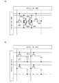
なお本実施の形態で開示するトランジスタの構造では、ソース電極及びドレイン電極となる第1の導電層405a及び第1の導電層405b間の距離Lcがトランジスタ420のチャネル長となる。本実施の形態で開示する構造において、ゲート電極層401のチャネル長方向の長さをLgとし、チャネル長をLcとすると、図3(A)に示すように同じ長さとなるか、若しくは図3(B)に示すようにLgがLcより長くなるように設けることができる。つまり、本実施の形態で開示するトランジスタの構造は、トランジスタのソース電極及びドレイン電極となる第1の導電層405a、405bの端部と、ゲート電極となるゲート電極層401の端部とを重畳して設けることができる構造である。そのため、トランジスタのオン特性(例えば、オン電流や電界効果移動度)を向上させて、半導体装置の高速応答、高速駆動を実現することができる。
以上の工程で、本実施の形態のトランジスタ420が作製される(図2(E)参照)。インジウム、亜鉛、及び酸素を少なくとも含む酸化物半導体層403を用い、トランジスタのソース電極及びドレイン電極と、ゲート電極とを重畳して設け、且つカバレッジを良好にしたトランジスタを実現できる。そして、トランジスタのオン特性を向上させて、半導体装置の高速応答、高速駆動を実現する際に、信頼性の高い構成を提供することができる。
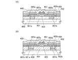
ここで、図1に示したトランジスタ420の変形例について、図4を用いて説明する。図4の説明において、図1と同一部分又は同様な機能を有する部分については、繰り返しの説明は省略する。また同じ箇所の詳細な説明は省略する。
図4に示すトランジスタの構造は、第1の導電層と第2の導電層とを直接積層する図1のトランジスタの構造と異なり、第1の導電層と第2の導電層との間に絶縁層を設ける構造である。
図4は、図1のトランジスタ420の構成とは異なる一例であるトランジスタ430の断面図である。
トランジスタ430は、絶縁表面を有する基板400上に、バッファ層436と、酸化物半導体層403と、第1の導電層405a、405bと、第2の導電層465a、465bと、絶縁層417と、ゲート絶縁層402と、ゲート電極層401と、層間絶縁層408と、を有する(図4参照)。
図4の構造は、図1の構造と同様に、トランジスタ430のソース電極及びドレイン電極として機能する第1の導電層405a、405bを、酸化物半導体層403と重畳する領域において、ゲート絶縁層402を介してゲート電極層401と重畳させている。また図4の構造は、図1の構造と同様に、トランジスタ430のソース電極及びドレイン電極として機能する第2の導電層465a、465bを、酸化物半導体層403と重畳する領域において、ゲート絶縁層402を介してゲート電極層401と重畳させない。
そのため図4の構造は、トランジスタのソース電極及びドレイン電極を流れる電流を低減させることなく、トランジスタのソース電極及びドレイン電極と、ゲート電極とを重畳して設けることができ、オン特性を向上させることができる。さらに図4の構成では、ゲート絶縁層のカバレッジ不良を低減することで、酸化物半導体層及びゲート絶縁層を薄膜化することができる。
また特に、図4の構造は、第1の導電層405a、405bと第2の導電層465a、465bとの間に絶縁層417を設け、開口部418において直接接続している。当該構造とすることで、トランジスタ430を作製する際、第1の導電層と第2の導電層とのエッチングの選択比が小さくても所定の形状に加工することができる。そのため、第1の導電層と第2の導電層に同じ材料を用いる構成とすることも可能である。
以上説明したように、本実施の形態で開示する構成では、トランジスタのソース電極及びドレイン電極を流れる電流を低減させることなく、トランジスタのソース電極及びドレイン電極と、ゲート電極とを重畳して設けることができ、オン特性を向上させることができる。さらに本実施の形態で開示する構成では、ゲート絶縁層のカバレッジ不良を低減することで、酸化物半導体層及びゲート絶縁層を薄膜化することができる。この場合、酸化物半導体をチャネル形成領域に設けるトランジスタを微細化して形成することができ好適である。
本実施の形態は、他の実施の形態と適宜組み合わせて実施することが可能である。
(実施の形態2)
本実施の形態では、半導体装置の他の一形態を、図5及び図6を用いて説明する。上記実施の形態と同一部分又は同様な機能を有する部分、及び工程は、上記実施の形態と同様に行うことができ、繰り返しの説明は省略する。また同じ箇所の詳細な説明は省略する。
図5(A)は、実施の形態1で示した半導体装置の構成とは異なる一例であるトランジスタ440の断面図である。
トランジスタ440は、絶縁表面を有する基板400上に、埋め込み導電層481a、481bが設けられた絶縁層491と、酸化物半導体層403と、第1の導電層405a、405bと、第2の導電層465a、465bと、ゲート絶縁層402と、ゲート電極層401と、層間絶縁層408と、を有する(図5(A)参照)。
図5(A)の構造は、図1の構造と同様に、トランジスタ440のソース電極及びドレイン電極として機能する第1の導電層405a、405bを、酸化物半導体層403と重畳する領域において、ゲート絶縁層402を介してゲート電極層401と重畳させている。また図5(A)の構造は、図1の構造と同様に、トランジスタ440のソース電極及びドレイン電極として機能する第2の導電層465a、465bを、酸化物半導体層403と重畳する領域において、ゲート絶縁層402を介してゲート電極層401と重畳させない。
そのため図5(A)の構造は、トランジスタのソース電極及びドレイン電極を流れる電流を低減させることなく、トランジスタのソース電極及びドレイン電極と、ゲート電極とを重畳して設けることができ、オン特性を向上させることができる。さらに図5(A)の構成では、ゲート絶縁層のカバレッジ不良を低減することで、酸化物半導体層及びゲート絶縁層を薄膜化することができる。
また特に、本実施の形態で開示する図5(A)の構造は、トランジスタ440の下部に埋め込み導電層481a、481bが設けられた絶縁層491を設け、埋め込み導電層481a、481bが、酸化物半導体層403を介して、第1の導電層405a、405bと、第2の導電層465a、465bとに重畳して設けられている。トランジスタ440の下部に埋め込み導電層481a、481bを設ける構成とすることで、ゲート絶縁層402及び層間絶縁層408に開口部を設けることなく、トランジスタ間及び外部に設けられた制御回路と接続することができる。埋め込み導電層481a、481bは、トランジスタ440との接触面積を大きくとることができるため、コンタクト抵抗を低減することができる。
なお埋め込み導電層481a、481bは、絶縁層491を形成した後に開口部を設け、該開口部を埋めるように埋め込み導電層を設けた後に、表面にCMP法による研磨を行って形成すればよい。
埋め込み導電層481a、481bとしては、例えば、Al、Cr、Cu、Ta、Ti、Mo、Wから選ばれた元素を含む金属膜、又は上述した元素を成分とする金属窒化物膜(窒化チタン膜、窒化モリブデン膜、窒化タングステン膜)等を用いることができる。
なお、Al、Cuなどの金属膜を埋め込み導電層481a、481bとして用いる場合には、該金属膜の下側又は上側の一方又は双方にTi、Mo、Wなどの高融点金属膜又はそれらの金属窒化物膜(窒化チタン膜、窒化モリブデン膜、窒化タングステン膜)を積層させた構成とすることが好ましい。
また、埋め込み導電層481a、481bとしては、導電性の金属酸化物で形成しても良い。導電性の金属酸化物としては酸化インジウム(In2O3)、酸化スズ(SnO2)、酸化亜鉛(ZnO)、酸化インジウム酸化スズ(In2O3―SnO2、ITOと略記する)、酸化インジウム酸化亜鉛(In2O3―ZnO)又はこれらの金属酸化物材料に酸化シリコンを含ませたものを用いることができる。
絶縁層491は、CVD法やスパッタリング法等を用いて成膜することができる。また、絶縁層491は、酸化シリコン、窒化シリコン、酸化窒化シリコン、窒化酸化シリコン、酸化アルミニウム、酸化ハフニウム、酸化タンタルなどを含むように成膜するのが好適である。なお、絶縁層491は、単層構造としても良いし、積層構造としても良い。
また図5(B)は、図5(A)と異なる構成である、トランジスタ450の断面図である。
トランジスタ450は、絶縁表面を有する基板400上に、埋め込み導電層481a、481b及び埋め込み酸化物半導体層482a、482bが設けられた絶縁層491と、酸化物半導体層403と、第1の導電層405a、405bと、第2の導電層465a、465bと、ゲート絶縁層402と、ゲート電極層401と、層間絶縁層408と、を有する(図5(B)参照)。
図5(B)の構造は、図1の構造と同様に、トランジスタ450のソース電極及びドレイン電極として機能する第1の導電層405a、405bを、酸化物半導体層403と重畳する領域において、ゲート絶縁層402を介してゲート電極層401と重畳させている。また図5(B)の構造は、図1の構造と同様に、トランジスタ450のソース電極及びドレイン電極として機能する第2の導電層465a、465bを、酸化物半導体層403と重畳する領域において、ゲート絶縁層402を介してゲート電極層401と重畳させない。
そのため図5(B)の構造は、トランジスタのソース電極及びドレイン電極を流れる電流を低減させることなく、トランジスタのソース電極及びドレイン電極と、ゲート電極とを重畳して設けることができ、オン特性を向上させることができる。さらに図5(B)の構成では、ゲート絶縁層のカバレッジ不良を低減することで、酸化物半導体層及びゲート絶縁層を薄膜化することができる。
また特に、本実施の形態で開示する図5(B)の構造は、トランジスタ450の下部に埋め込み導電層481a、481b及び埋め込み酸化物半導体層482a、482bが設けられた絶縁層491を設け、埋め込み導電層481a、481b及び埋め込み酸化物半導体層482a、482bが、酸化物半導体層403を介して、第1の導電層405a、405bと、第2の導電層465a、465bとに重畳して設けられている。トランジスタ450の下部に埋め込み導電層481a、481bを設ける構成とすることで、ゲート絶縁層402及び層間絶縁層408に開口部を設けることなく、トランジスタ間及び外部に設けられた制御回路と接続することができる。また埋め込み導電層481a、481bとトランジスタ450との間に埋め込み酸化物半導体層482a、482bを設ける構成とすることで、埋め込み導電層481a、481bとトランジスタ450との接続を良好なものとすることができる。埋め込み導電層481a、481bは、トランジスタ450との接触面積を大きくとることができ、加えて埋め込み酸化物半導体層482a、482bはトランジスタ450との接続を良好なものとすることができるため、コンタクト抵抗を低減することができる。
埋め込み酸化物半導体層482a、482bとしては、少なくともインジウム(In)あるいは亜鉛(Zn)を含むことが好ましい。特にInとZnを含むことが好ましい。また、該酸化物半導体を用いたトランジスタの電気特性のばらつきを減らすためのスタビライザーとして、それらに加えてガリウム(Ga)を有することが好ましい。また、スタビライザーとしてスズ(Sn)を有することが好ましい。また、スタビライザーとしてハフニウム(Hf)を有することが好ましい。また、スタビライザーとしてアルミニウム(Al)を有することが好ましい。また、スタビライザーとしてジルコニウム(Zr)を有することが好ましい。
また、埋め込み酸化物半導体層482a、482bとしては、酸化物半導体層に導電性を付与した金属酸化物で形成しても良い。導電性の金属酸化物としては酸化インジウム(In2O3)、酸化スズ(SnO2)、酸化亜鉛(ZnO)、酸化インジウム酸化スズ(In2O3―SnO2、ITOと略記する)、酸化インジウム酸化亜鉛(In2O3―ZnO)又はこれらの金属酸化物材料に酸化シリコンを含ませたものを用いることができる。
また図6(A)は図5(A)で示した半導体装置の構成とは異なる一例であるトランジスタ460の断面図である。
トランジスタ460は、絶縁表面を有する基板400上に、埋め込み導電層481a、481bが設けられた絶縁層491と、酸化物半導体層403と、第1の導電層405a、405bと、第2の導電層465a、465bと、ゲート絶縁層402と、ゲート電極層401と、層間絶縁層408と、を有する(図6(A)参照)。
図6(A)の構造は、図1の構造と同様に、トランジスタ460のソース電極及びドレイン電極として機能する第1の導電層405a、405bを、酸化物半導体層403と重畳する領域において、ゲート絶縁層402を介してゲート電極層401と重畳させている。また図6(A)の構造は、図1の構造と同様に、トランジスタ460のソース電極及びドレイン電極として機能する第2の導電層465a、465bを、酸化物半導体層403と重畳する領域において、ゲート絶縁層402を介してゲート電極層401と重畳させない。
そのため図6(A)の構造は、トランジスタのソース電極及びドレイン電極を流れる電流を低減させることなく、トランジスタのソース電極及びドレイン電極と、ゲート電極とを重畳して設けることができ、オン特性を向上させることができる。さらに図6(A)の構成では、ゲート絶縁層のカバレッジ不良を低減することで、酸化物半導体層及びゲート絶縁層を薄膜化することができる。
また特に、本実施の形態で開示する図6(A)の構造は、図5(A)の構造と同様に、トランジスタ460の下部に埋め込み導電層481a、481bが設けられた絶縁層491を設け、埋め込み導電層481a、481bが、酸化物半導体層403を介して、第1の導電層405a、405bと、第2の導電層465a、465bとに重畳して設けられている。トランジスタ460の下部に埋め込み導電層481a、481bを設ける構成とすることで、ゲート絶縁層402及び層間絶縁層408に開口部を設けることなく、トランジスタ間及び外部に設けられた制御回路とを接続することができる。埋め込み導電層481a、481bは、トランジスタ460との接触面積を大きくとることができるため、コンタクト抵抗を低減することができる。
また特に、本実施の形態で開示する図6(A)の構造は、酸化物半導体層403に開口部485を設け、第1の導電層405a、405bと、埋め込み導電層481a、481bとを直接接続する構造としている。該構造とすることにより、トランジスタのソース電極及びドレイン電極となる第1の導電層、第2の導電層及び埋め込み導電層を流れる電流を大きくすることができる。
また図6(B)は、図6(A)と異なる構成である、トランジスタ470の断面図である。
トランジスタ470は、絶縁表面を有する基板400上に、埋め込み導電層481a、481b及び埋め込み酸化物半導体層482a、482bが設けられた絶縁層491と、酸化物半導体層403と、第1の導電層405a、405bと、第2の導電層465a、465bと、ゲート絶縁層402と、ゲート電極層401と、層間絶縁層408と、を有する(図6(B)参照)。
図6(B)の構造は、図1の構造と同様に、トランジスタ470のソース電極及びドレイン電極として機能する第1の導電層405a、405bを、酸化物半導体層403と重畳する領域において、ゲート絶縁層402を介してゲート電極層401と重畳させる。また図6(B)の構造は図1の構造と同様に、トランジスタ470のソース電極及びドレイン電極として機能する第2の導電層465a、465bを、酸化物半導体層403と重畳する領域において、ゲート絶縁層402を介してゲート電極層401と重畳させない。
そのため図6(B)の構造は、トランジスタのソース電極及びドレイン電極を流れる電流を低減させることなく、トランジスタのソース電極及びドレイン電極と、ゲート電極とを重畳して設けることができ、オン特性を向上させることができる。さらに図6(B)の構成では、ゲート絶縁層のカバレッジ不良を低減することで、酸化物半導体層及びゲート絶縁層を薄膜化することができる。
また特に、本実施の形態で開示する図6(B)の構造は、トランジスタ470の下部に埋め込み導電層481a、481b及び埋め込み酸化物半導体層482a、482bが設けられた絶縁層491を設け、埋め込み導電層481a、481b及び埋め込み酸化物半導体層482a、482bが、酸化物半導体層403を介して、第1の導電層405a、405bと、第2の導電層465a、465bとに重畳して設けられている。トランジスタ470の下部に埋め込み導電層481a、481bを設ける構成とすることで、ゲート絶縁層402及び層間絶縁層408に開口部を設けることなく、トランジスタ間及び外部に設けられる制御回路と接続することができる。また埋め込み導電層481a、481bとトランジスタ470との間に埋め込み酸化物半導体層482a、482bを設ける構成とすることで、埋め込み導電層481a、481bとトランジスタ470との接続を良好なものとすることができる。埋め込み導電層481a、481bは、トランジスタ470との接触面積を大きくとることができ、加えて埋め込み酸化物半導体層482a、482bはトランジスタ470との接続を良好なものとすることができるため、コンタクト抵抗を低減することができる。
また特に本実施の形態で開示する図6(B)の構造は、酸化物半導体層403に開口部485を設け、第1の導電層405a、405bと、埋め込み酸化物半導体層482a、482bとを直接接続する構造としている。該構造とすることにより、トランジスタのソース電極及びドレイン電極となる第1の導電層、第2の導電層、埋め込み酸化物半導体層及び埋め込み導電層を流れる電流を大きくすることができる。
以上説明したように、本実施の形態の構成では、上記実施の形態1と同様に、トランジスタのソース電極及びドレイン電極を流れる電流を低減させることなく、トランジスタのソース電極及びドレイン電極と、ゲート電極とを重畳して設けることができ、オン特性を向上させることができる。さらに本実施の形態の構成では、ゲート絶縁層のカバレッジ不良を低減することで、酸化物半導体層及びゲート絶縁層を薄膜化することができる。この場合、酸化物半導体をチャネル形成領域に設けるトランジスタを微細化して形成することができ好適である。また、特に本実施の形態の構成では、埋め込み導電層を設け、トランジスタとのコンタクト抵抗を低減することができる。
本実施の形態は、他の実施の形態と適宜組み合わせて実施することが可能である。
(実施の形態3)
本実施の形態では、半導体装置の他の一形態を、図7を用いて説明する。上記実施の形態と同一部分又は同様な機能を有する部分、及び工程は、上記実施の形態と同様に行うことができ、繰り返しの説明は省略する。また同じ箇所の詳細な説明は省略する。
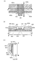
本実施の形態において図7(A)は、実施の形態1で示した図1によるトランジスタ420の平面図であり、図7(B)は、図7(A)のX−Yにおける断面図であり、図7(C)は、図7(A)のV−Wにおける断面図である。
図7(A)乃至(C)に示すトランジスタ420の構成は、図1と同様に、絶縁表面を有する基板400上に、バッファ層436と、酸化物半導体層403と、第1の導電層405a、405bと、第2の導電層465a、465bと、絶縁層407と、ゲート絶縁層402と、ゲート電極層401と、層間絶縁層408と、を有する。
本実施の形態で開示する図7(A)乃至(C)の構造は、図1と同様に、トランジスタ420のソース電極及びドレイン電極として機能する第1の導電層405a、405bを、酸化物半導体層403と重畳する領域において、ゲート絶縁層402を介してゲート電極層401と重畳させている。また本実施の形態で開示する図7(A)乃至(C)の構造は、トランジスタ420のソース電極及びドレイン電極として機能する第2の導電層465a、465bを、酸化物半導体層403と重畳する領域において、ゲート絶縁層402を介してゲート電極層401と重畳させない。
本実施の形態で開示する図7(A)乃至(C)の構造は、トランジスタのソース電極及びドレイン電極となる第1の導電層405a、405bの端部と、ゲート電極となるゲート電極層401の端部とを重畳して設けることができる。そのため、トランジスタのオン特性(例えば、オン電流や電界効果移動度)を向上させて、半導体装置の高速応答、高速駆動を実現することができる。
また本実施の形態で開示する図7(A)乃至(C)の構造は、トランジスタのソース電極及びドレイン電極となる第1の導電層405a、405bを薄膜化することができる。第1の導電層405a、405bを薄膜化することで、特に酸化物半導体層403のチャネル形成領域周辺での、ゲート絶縁層402を形成する際の表面の段差を小さくすることができる。従って、ゲート絶縁層402は、カバレッジを良好にして形成することができる。カバレッジ不良を低減することで、電極間の短絡の発生を抑制し、信頼性の向上を図ることができる。
また、第1の導電層405a、405bを薄膜化することで、酸化物半導体層403上に形成された第1の導電層405の厚さを均一にしておくことが可能になる。また第1の導電層405を薄膜化して形成しておくことで、エッチング等の工程により第1の導電層405a、405bを加工する際の所要期間を短くすることができる。そのため第1の導電層405a、405bをエッチング等の工程で加工する際に生じる、酸化物半導体層403へのダメージを低減することができる。そのため、信頼性の向上を図ることができる。
また本実施の形態で開示する図7(A)乃至(C)の構造は、ゲート絶縁層402を薄膜化するとともに、酸化物半導体層403を薄膜化することができる。ゲート絶縁層402及び酸化物半導体層403を薄膜化することで、オン特性の向上が図れるとともに、トランジスタを完全空乏型で動作させることも可能である。トランジスタを完全空乏型で動作させることで、高集積化、高速駆動化、低消費電力化を図ることができる。
加えて、本実施の形態で開示する図7(A)乃至(C)の構造は、トランジスタのソース電極及びドレイン電極となる第2の導電層465a、465bの端部と、ゲート電極となるゲート電極層401の端部とを重畳させないで設けることができる。そのため、第1の導電層405a、405bに比べて第2の導電層465a、465bを厚膜化しても、電極間の短絡がない。したがって、第2の導電層465a、465bを厚膜化することで、電極間での短絡を引き起こすことなく、ソース電極及びドレイン電極を流れる電流を大きくすることができる。
また本実施の形態で開示する図7(A)乃至(C)の構造は、第2の導電層465a、465bと絶縁層407とを重畳して設け、側面をエッチング等の加工によりテーパー状とすることができる。そのため第2の導電層465a、465bを厚膜化しても、カバレッジを良好にすることができる。
以上説明したように、本実施の形態で開示する図7(A)乃至(C)の構成では、トランジスタのソース電極及びドレイン電極を流れる電流を低減させることなく、トランジスタのソース電極及びドレイン電極と、ゲート電極とを重畳して設けることができ、オン特性を向上させることができる。さらに本実施の形態で開示する図7(A)乃至(C)の構成では、ゲート絶縁層のカバレッジ不良を低減することで、酸化物半導体層及びゲート絶縁層を薄膜化することができる。この場合、酸化物半導体をチャネル形成領域に設けるトランジスタを微細化して形成することができ好適である。
本実施の形態は、他の実施の形態と適宜組み合わせて実施することが可能である。
(実施の形態4)
本実施の形態では、実施の形態1乃至3に示すトランジスタを使用し、電力が供給されない状況でも記憶内容の保持が可能で、かつ、書き込み回数にも制限が無い半導体装置の一例を、図面を用いて説明する。なお、本実施の形態の半導体装置は、トランジスタ162として実施の形態1乃至3に記載のトランジスタを適用して構成される。
トランジスタ162は、オフ電流が小さいため、これを用いることにより長期にわたり記憶内容を保持することが可能である。つまり、リフレッシュ動作を必要としない、或いは、リフレッシュ動作の頻度が極めて少ない半導体記憶装置とすることが可能となるため、消費電力を十分に低減することができる。
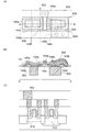
図8は、半導体装置の構成の一例である。図8(A)に、半導体装置の断面図を、図8(B)に半導体装置の平面図を、図8(C)に半導体装置の回路図をそれぞれ示す。ここで、図8(A)は、図8(B)のC1−C2、及びD1−D2における断面に相当する。
図8(A)及び図8(B)に示す半導体装置は、下部に第1の半導体材料を用いたトランジスタ160を有し、上部に第2の半導体材料を用いたトランジスタ162を有するものである。トランジスタ162は、実施の形態1乃至3で示した構成と同一の構成とすることができる。
ここで、第1の半導体材料と第2の半導体材料は異なる禁制帯幅を持つ材料とすることが望ましい。例えば、第1の半導体材料を酸化物半導体以外の半導体材料(シリコンなど)とし、第2の半導体材料を酸化物半導体とすることができる。酸化物半導体以外の材料を用いたトランジスタは、高速動作が容易である。一方で、酸化物半導体を用いたトランジスタは、その特性により長時間の電荷保持を可能とする。
なお、上記トランジスタは、いずれもnチャネル型トランジスタであるものとして説明するが、pチャネル型トランジスタを用いることができるのはいうまでもない。また、開示する発明の技術的な本質は、情報を保持するために酸化物半導体をトランジスタ162に用いる点にあるから、半導体装置に用いられる材料や半導体装置の構造など、半導体装置の具体的な構成をここで示すものに限定する必要はない。
図8(A)におけるトランジスタ160は、半導体材料(例えば、シリコンなど)を含む基板100に設けられたチャネル形成領域116と、チャネル形成領域116を挟むように設けられた不純物領域120と、不純物領域120に接する金属間化合物領域124と、チャネル形成領域116上に設けられたゲート絶縁層108と、ゲート絶縁層108上に設けられたゲート電極層110と、を有する。
基板100上にはトランジスタ160を囲むように素子分離絶縁層106が設けられており、トランジスタ160を覆うように絶縁層128及び層間絶縁層130が設けられている。なお、高集積化を実現するためには、図8(A)に示すようにトランジスタ160がサイドウォール絶縁層を有しない構成とすることが望ましい。一方で、トランジスタ160の特性を重視する場合には、ゲート電極層110の側面にサイドウォール絶縁層を設け、不純物濃度が異なる領域を含む不純物領域120としてもよい。
図8(A)に示すトランジスタ162は、酸化物半導体をチャネル形成領域に用いたトランジスタである。ここで、トランジスタ162に含まれる酸化物半導体層144は、高純度化されたものであることが望ましい。高純度化された酸化物半導体を用いることで、極めて優れたオフ特性のトランジスタ162を得ることができる。
トランジスタ162上には、絶縁層150が単層又は積層で設けられている。また、絶縁層150を介して、トランジスタ162の電極層となる第1の導電層140a及び第2の導電層141aと重畳する領域には、導電層148bが設けられており、第1の導電層140a及び第2の導電層141aと、絶縁層142及び絶縁層150と、導電層148bとによって、容量素子164が構成される。すなわち、トランジスタ162の第1の導電層140a及び第2の導電層141aは、容量素子164の一方の電極として機能し、導電層148bは、容量素子164の他方の電極として機能する。なお、容量が不要の場合には、容量素子164を設けない構成とすることもできる。また、容量素子164は、別途、トランジスタ162の上方に設けてもよい。
トランジスタ162および容量素子164の上には絶縁層152が設けられている。そして、絶縁層152上にはトランジスタ162と、他のトランジスタを接続するための配線156が設けられている。図8(A)には図示しないが、配線156は、絶縁層150、絶縁層152及びゲート絶縁層146などに形成された開口に形成された電極を介して第2の導電層141a及び第2の導電層141bに接続される。
ここで、第1の導電層140a及び第1の導電層140bは、実施の形態1で説明したように、トランジスタ162のゲート電極となる導電層148aの一部と重畳するように設ける。また第2の導電層141a及び第2の導電層141bは、実施の形態1で説明したように、トランジスタ162のゲート電極となる導電層148aの一部と重畳しないように設ける。その結果、トランジスタのソース電極及びドレイン電極を流れる電流を低減させることなく、トランジスタのソース電極及びドレイン電極と、ゲート電極とを重畳して設けることができ、オン特性を向上させることができる。また、ゲート絶縁層のカバレッジ不良を低減することで、酸化物半導体層及びゲート絶縁層を薄膜化することができ、トランジスタを微細化して形成することができる。
図8(A)及び図8(B)において、トランジスタ160と、トランジスタ162とは、少なくとも一部が重畳するように設けられており、トランジスタ160のソース領域又はドレイン領域と酸化物半導体層144の一部が重畳するように設けられているのが好ましい。また、トランジスタ162及び容量素子164が、トランジスタ160の少なくとも一部と重畳するように設けられている。例えば、容量素子164の一方の電極である第1の導電層140aは、トランジスタ160のゲート電極層110と少なくとも一部が重畳して設けられている。このような平面レイアウトを採用することにより、半導体装置の占有面積の低減を図ることができるため、高集積化を図ることができる。
次に、図8(A)及び図8(B)に対応する回路構成の一例を図8(C)に示す。
図8(C)において、第1の配線(1st Line)は、トランジスタ160のソース電極に接続されている。また第2の配線(2nd Line)は、トランジスタ160のドレイン電極に接続されている。また、第3の配線(3rd Line)は、トランジスタ162のソース電極又はドレイン電極の一方に接続されている。また第4の配線(4th Line)は、トランジスタ162のゲート電極に接続されている。またトランジスタ160のゲート電極は、トランジスタ162のソース電極又はドレイン電極の一方と、容量素子164の電極の一方とに接続されている。また第5の配線(5th Line)は、容量素子164の電極の他方に接続されている。
図8(C)に示す半導体装置では、トランジスタ160のゲート電極の電位が保持可能という特徴を生かすことで、次のように、情報の書き込み、保持、読み出しが可能である。
情報の書き込みおよび保持について説明する。まず、第4の配線の電位を、トランジスタ162がオン状態となる電位にして、トランジスタ162をオン状態とする。これにより、第3の配線の電位が、トランジスタ160のゲート電極、および容量素子164の一方の電極に与えられる。すなわち、トランジスタ160のゲート電極には、所定の電荷が与えられる(書き込み)。ここでは、異なる二つの電位レベル(Hレベル、Lレベル)のいずれかが与えられるものとする。その後、第4の配線の電位を、トランジスタ162がオフ状態となる電位にして、トランジスタ162をオフ状態とすることにより、トランジスタ160のゲート電極に与えられた電位が保持される(保持)。
トランジスタ162のオフ電流は極めて小さいため、トランジスタ160のゲート電極の電荷は長時間にわたって保持される。
次に情報の読み出しについて説明する。第1の配線に所定の電位(定電位)を与えた状態で、第5の配線に適切な電位(読み出し電位)を与えると、トランジスタ160のゲート電極の電位に応じて、第2の配線は異なる電位をとる。該異なる電位は、トランジスタ160をnチャネル型とすると、トランジスタ160のゲート電極にHレベルが与えられている場合の見かけのしきい値電圧Vth_Hが、トランジスタ160のゲート電極にLレベルが与えられている場合の見かけのしきい値電圧Vth_Lより低くなるためである。ここで、見かけのしきい値電圧とは、トランジスタ160を「オン状態」とするために必要な第5の配線の電位をいうものとする。したがって、第5の配線の電位をVth_HとVth_Lの間の電位V0とすることにより、トランジスタ160のゲート電極に与えられた電荷を判別できる。例えば、書き込みにおいて、Hレベルが与えられていた場合には、第5の配線の電位がV0(>Vth_H)となれば、トランジスタ160は「オン状態」となる。Lレベルが与えられていた場合には、第5の配線の電位がV0(<Vth_L)となっても、トランジスタ160は「オフ状態」のままである。このため、第2の配線の電位を見ることで、保持されている情報を読み出すことができる。
なお、メモリセルをアレイ状に配置して用いる場合、所望のメモリセルの情報のみを読み出せることが必要になる。このように情報を読み出さない場合には、ゲート電極の状態にかかわらずトランジスタ160が「オフ状態」となるような電位、つまり、Vth_Hより小さい電位を第5の配線に与えればよい。又は、ゲート電極の状態にかかわらずトランジスタ160が「オン状態」となるような電位、つまり、Vth_Lより大きい電位を第5の配線に与えればよい。
本実施の形態に示す半導体装置では、チャネル形成領域に酸化物半導体を用いたオフ電流の極めて小さいトランジスタを適用することで、極めて長期にわたり記憶内容を保持することが可能である。つまり、リフレッシュ動作が不要となるか、又は、リフレッシュ動作の頻度を極めて低くすることが可能となるため、消費電力を十分に低減することができる。また、電力の供給がない場合(ただし、電位は固定されていることが望ましい)であっても、長期にわたって記憶内容を保持することが可能である。
また、本実施の形態に示す半導体装置では、情報の書き込みに高い電圧を必要とせず、素子の劣化の問題もない。例えば、従来の不揮発性メモリのように、フローティングゲートへの電子の注入や、フローティングゲートからの電子の引き抜きを行う必要がないため、ゲート絶縁層の劣化といった問題が全く生じない。すなわち、開示する発明に係る半導体装置では、従来の不揮発性メモリで問題となっている書き換え可能回数に制限はなく、信頼性が飛躍的に向上する。さらに、トランジスタのオン状態、オフ状態によって、情報の書き込みが行われるため、高速な動作も容易に実現しうる。
本実施の形態は、他の実施の形態と適宜組み合わせて実施することが可能である。
(実施の形態5)
本実施の形態においては、実施の形態1乃至3に示すトランジスタを使用し、電力が供給されない状況でも記憶内容の保持が可能で、かつ、書き込み回数にも制限が無い半導体装置について、実施の形態4に示した構成と異なる構成を図9及び図10を用いて説明する。なお、本実施の形態の半導体装置は、トランジスタ162として実施の形態1乃至3に記載のトランジスタを適用して構成される。
図9(A)は、半導体装置の回路構成の一例を示し、図9(B)は半導体装置の一例を示す概念図である。まず、図9(A)に示す半導体装置について説明を行い、続けて図9(B)に示す半導体装置について、以下説明を行う。
図9(A)に示す半導体装置において、ビット線BLは、トランジスタ162のソース電極又はドレイン電極となる一方の電極に接続される。ワード線WLは、トランジスタ162のゲート電極に接続される。トランジスタ162のソース電極又はドレイン電極となる他方の電極は、容量素子254の一方の電極に接続される。
酸化物半導体を用いたトランジスタ162は、オフ電流が極めて小さいという特徴を有している。このため、トランジスタ162をオフ状態とすることで、容量素子254の一方の電極の電位(あるいは、容量素子254に蓄積された電荷)を極めて長時間にわたって保持することが可能である。
次に、図9(A)に示す半導体装置(メモリセル250)に、情報の書き込みおよび保持を行う場合について説明する。
まず、ワード線WLの電位を、トランジスタ162がオン状態となる電位として、トランジスタ162をオン状態とする。これにより、ビット線BLの電位が、容量素子254の一方の電極に与えられる(書き込み)。その後、ワード線WLの電位を、トランジスタ162がオフ状態となる電位として、トランジスタ162をオフ状態とすることにより、容量素子254の一方の電極の電位が保持される(保持)。
トランジスタ162のオフ電流は極めて小さいため、容量素子254の一方の電極の電位(あるいは容量素子に蓄積された電荷)は長時間にわたって保持することができる。
次に、情報の読み出しについて説明する。トランジスタ162がオン状態となると、浮遊状態であるビット線BLと容量素子254の一方の電極とが導通し、ビット線BLと容量素子254の一方の電極の間で電荷が再分配される。その結果、ビット線BLの電位が変化する。ビット線BLの電位の変化量は、容量素子254の一方の電極の電位(あるいは容量素子254に蓄積された電荷)によって、異なる値をとる。
例えば、容量素子254の一方の電極の電位をV、容量素子254の静電容量をC、ビット線BLが有する静電容量成分(以下、ビット線容量とも呼ぶ)をCB、電荷が再分配される前のビット線BLの電位をVB0とすると、電荷が再分配された後のビット線BLの電位は、(CB×VB0+C×V)/(CB+C)となる。したがって、メモリセル250の状態として、容量素子254の一方の電極の電位がV1とV0(V1>V0)の2状態をとるとすると、電位V1を保持している場合のビット線BLの電位(=CB×VB0+C×V1)/(CB+C))は、電位V0を保持している場合のビット線BLの電位(=CB×VB0+C×V0)/(CB+C))よりも高くなることがわかる。
そして、ビット線BLの電位を所定の電位と比較することで、情報を読み出すことができる。
このように、図9(A)に示す半導体装置は、トランジスタ162のオフ電流が極めて小さいという特徴から、容量素子254に蓄積された電荷は長時間にわたって保持することができる。つまり、リフレッシュ動作が不要となるか、又は、リフレッシュ動作の頻度を極めて低くすることが可能となるため、消費電力を十分に低減することができる。また、電力の供給がない場合であっても、長期にわたって記憶内容を保持することが可能である。
次に、図9(B)に示す半導体装置について、説明を行う。
図9(B)に示す半導体装置は、上部に記憶回路として図9(A)に示したメモリセル250を複数有するメモリセルアレイ251a及び251bを有し、下部に、メモリセルアレイ251a及びメモリセルアレイ251bを動作させるために必要な周辺回路253を有する。なお、周辺回路253は、メモリセルアレイ251(メモリセルアレイ251a及び251b)に接続されている。
図9(B)に示した構成とすることにより、周辺回路253をメモリセルアレイ251の直下に設けることができるため半導体装置の小型化を図ることができる。
周辺回路253に設けられるトランジスタは、トランジスタ162とは異なる半導体材料を用いるのがより好ましい。例えば、シリコン、ゲルマニウム、シリコンゲルマニウム、炭化シリコン、又はガリウムヒ素等を用いることができ、単結晶半導体を用いることが好ましい。他に、有機半導体材料などを用いてもよい。このような半導体材料を用いたトランジスタは、十分な高速動作が可能である。したがって、該トランジスタにより、高速動作が要求される各種回路(論理回路、駆動回路など)を好適に実現することが可能である。
なお、図9(B)に示した半導体装置では、2つのメモリセルアレイ(メモリセルアレイ251aと、メモリセルアレイ251b)が積層された構成を例示したが、積層するメモリセルアレイの数はこれに限定されない。3つ以上のメモリセルアレイを積層する構成としても良い。
次に、図9(A)に示したメモリセル250の具体的な構成について図10を用いて説明を行う。
図10は、メモリセル250の構成の一例である。図10(A)に、メモリセル250の平面図を、図10(B)に図10(A)の線分A−Bにおける断面図をそれぞれ示す。
図10(A)及び図10(B)に示すトランジスタ162は、実施の形態1乃至3で示したトランジスタの構成と同一の構成とすることができる。
図10(B)に示すように、埋め込み導電層502及び埋め込み導電層504上にトランジスタ162が設けられている。埋め込み導電層502は、図10(A)におけるビット線BLとして機能する配線であり、トランジスタ162の第1の導電層145aと接して設けられている。また、埋め込み導電層504は、図10(A)における容量素子254の一方の電極として機能し、トランジスタ162の第1の導電層145bと接して設けられている。また、トランジスタ162の第1の導電層145a上には、第2の導電層146aが接して設けられている。また、トランジスタ162の第1の導電層145b上には、第2の導電層146bが接して設けられている。またトランジスタ162上において、第2の導電層146bは、容量素子254の一方の電極として機能する。またトランジスタ162上において、第2の導電層146bと重畳する領域に設けられた導電層506は、容量素子254の他方の電極として機能する。
また、図10(A)に示すように、容量素子254の他方の導電層506は、容量線508に接続される。ゲート絶縁層147を介して酸化物半導体層144上に設けられたゲート電極として機能する導電層148aは、ワード線509に接続される。
また、図10(C)に、メモリセルアレイ251と、周辺回路との接続部における断面図を示す。周辺回路は、例えばnチャネル型トランジスタ510及びpチャネル型トランジスタ512を含む構成とすることができる。nチャネル型トランジスタ510及びpチャネル型トランジスタ512に用いる半導体材料としては、酸化物半導体以外の半導体材料(シリコンなど)を用いるのが好ましい。このような材料を用いることで、周辺回路に含まれるトランジスタの高速動作を図ることができる。
図10(A)に示す平面レイアウトを採用することにより、半導体装置の占有面積の低減を図ることができるため、高集積化を図ることができる。
以上のように、上部に多層に形成された複数のメモリセルは、酸化物半導体を用いたトランジスタにより形成されている。インジウム、亜鉛、及び酸素を少なくとも含む非単結晶の酸化物半導体を用いたトランジスタは、オフ電流が小さいため、これを用いることにより長期にわたり記憶内容を保持することが可能である。つまり、リフレッシュ動作の頻度を極めて低くすることが可能となるため、消費電力を十分に低減することができる。また、容量素子254は、図10(B)で示すように埋め込み導電層504、酸化物半導体層144、ゲート絶縁層147、導電層506が積層されることによって形成される。
このように、酸化物半導体以外の材料を用いたトランジスタを用いた周辺回路と、酸化物半導体を用いたトランジスタを用いた記憶回路とを一体に備えることで、これまでにない特徴を有する半導体装置を実現することができる。また、周辺回路と記憶回路を積層構造とすることにより、半導体装置の集積化を図ることができる。
本実施の形態は、他の実施の形態と適宜組み合わせて実施することが可能である。
(実施の形態6)
本実施の形態では、先の実施の形態で示した半導体装置を携帯電話、スマートフォン、電子書籍などの携帯機器に応用した場合の例を図11乃至図14を用いて説明する。
携帯電話、スマートフォン、電子書籍などの携帯機器においては、画像データの一時記憶などにSRAM又はDRAMが使用されている。SRAM又はDRAMが使用される理由としてはフラッシュメモリでは応答が遅く、画像処理では不向きであるためである。一方で、SRAM又はDRAMを画像データの一時記憶に用いた場合、以下の特徴がある。
通常のSRAMは、図11(A)に示すように1つのメモリセルがトランジスタ801〜806の6個のトランジスタで構成されており、それをXデコーダー807、Yデコーダー808にて駆動している。トランジスタ803とトランジスタ805、トランジスタ804とトランジスタ806はインバータを構成し、高速駆動を可能としている。しかし1つのメモリセルが6トランジスタで構成されているため、セル面積が大きいという欠点がある。デザインルールの最小寸法をFとしたときにSRAMのメモリセル面積は通常100〜150F2である。このためSRAMはビットあたりの単価が各種メモリの中で最も高い。
それに対して、DRAMはメモリセルが図11(B)に示すようにトランジスタ811、保持容量812によって構成され、それをXデコーダー813、Yデコーダー814にて駆動している。1つのセルが1トランジスタ1容量の構成になっており、面積が小さい。DRAMのメモリセル面積は通常10F2以下である。ただし、DRAMは常にリフレッシュが必要であり、書き換えをおこなわない場合でも電力を消費する。
しかし、先の実施の形態で説明した半導体装置のメモリセル面積は、10F2前後であり、且つ頻繁なリフレッシュは不要である。したがって、メモリセル面積が縮小され、且つ消費電力が低減することができる。
図12に携帯機器のブロック図を示す。図12に示す携帯機器はRF回路901、アナログベースバンド回路902、デジタルベースバンド回路903、バッテリー904、電源回路905、アプリケーションプロセッサ906、フラッシュメモリ910、ディスプレイコントローラ911、メモリ回路912、ディスプレイ913、タッチセンサ919、音声回路917、キーボード918などより構成されている。ディスプレイ913は表示部914、ソースドライバ915、ゲートドライバ916によって構成されている。アプリケーションプロセッサ906はCPU907、DSP908、インターフェイス909を有している。一般にメモリ回路912はSRAM又はDRAMで構成されており、この部分に先の実施の形態で説明した半導体装置を採用することによって、情報の書き込みおよび読み出しが高速で、長期間の記憶保持が可能で、且つ消費電力が十分に低減することができる。
図13に、ディスプレイのメモリ回路950に先の実施の形態で説明した半導体装置を使用した例を示す。図13に示すメモリ回路950は、メモリ952、メモリ953、スイッチ954、スイッチ955およびメモリコントローラ951により構成されている。また、メモリ回路は、画像データ(入力画像データ)を送る 信号線、メモリ952、及びメモリ953に記憶されたデータ(記憶画像データ)を読み出し、及び制御を行うディスプレイコントローラ956と、ディスプレイコントローラ956からの信号により表示するディスプレイ957が接続されている。
まず、ある画像データがアプリケーションプロセッサ(図示しない)によって、形成される(入力画像データA)。入力画像データAは、スイッチ954を介してメモリ952に記憶される。そしてメモリ952に記憶された画像データ(記憶画像データA)は、スイッチ955、及びディスプレイコントローラ956を介してディスプレイ957に送られ、表示される。
入力画像データAに変更が無い場合、記憶画像データAは、通常30〜60Hz程度の周期でメモリ952からスイッチ955を介して、ディスプレイコントローラ956から読み出される。
次に、例えばユーザーが画面を書き換える操作をしたとき(すなわち、入力画像データAに変更が有る場合)、アプリケーションプロセッサは新たな画像データ(入力画像データB)を形成する。入力画像データBはスイッチ954を介してメモリ953に記憶される。この間も定期的にメモリ952からスイッチ955を介して記憶画像データAは読み出されている。メモリ953に新たな画像データ(記憶画像データB)が記憶し終わると、ディスプレイ957の次のフレームより、記憶画像データBは読み出され、スイッチ955、及びディスプレイコントローラ956を介して、ディスプレイ957に記憶画像データBが送られ、表示がおこなわれる。この読み出しはさらに次に新たな画像データがメモリ952に記憶されるまで継続される。
このようにメモリ952及びメモリ953は交互に画像データの書き込みと、画像データの読み出しを行うことによって、ディスプレイ957の表示をおこなう。なお、メモリ952及びメモリ953はそれぞれ別のメモリには限定されず、1つのメモリを分割して使用してもよい。先の実施の形態で説明した半導体装置をメモリ952及びメモリ953に採用することによって、情報の書き込みおよび読み出しが高速で、長期間の記憶保持が可能で、且つ消費電力が十分に低減することができる。
図14に電子書籍のブロック図を示す。図14に示す電子書籍はバッテリー1001、電源回路1002、マイクロプロセッサ1003、フラッシュメモリ1004、音声回路1005、キーボード1006、メモリ回路1007、タッチパネル1008、ディスプレイ1009、ディスプレイコントローラ1010によって構成される。
ここでは、図14のメモリ回路1007に先の実施の形態で説明した半導体装置を使用することができる。メモリ回路1007の役割は書籍の内容を一時的に保持する機能を持つ。機能の例としては、ユーザーがハイライト機能を使用する場合などがある。ユーザーが電子書籍を読んでいるときに、特定の箇所にマーキングをしたい場合がある。このマーキング機能をハイライト機能と言い、表示の色を変える、アンダーラインを引く、文字を太くする、文字の書体を変えるなどによって、周囲との違いを示すことである。ユーザーが指定した箇所の情報を記憶し、保持する機能である。この情報を長期に保存する場合にはフラッシュメモリ1004にコピーしても良い。このような場合においても、先の実施の形態で説明した半導体装置を採用することによって、情報の書き込みおよび読み出しが高速で、長期間の記憶保持が可能で、且つ消費電力が十分に低減することができる。
以上のように、本実施の形態に示す携帯機器には、先の実施の形態に係る半導体装置が搭載されている。このため、読み出しが高速で、長期間の記憶保持が可能で、且つ消費電力を低減した携帯機器が実現される。
本実施の形態は、他の実施の形態と適宜組み合わせて実施することが可能である。
(実施の形態7)
本発明の一態様に係る半導体装置は、表示機器、パーソナルコンピュータ、記録媒体を備えた画像再生装置(代表的にはDVD:Digital Versatile Disc等の記録媒体を再生し、その画像を表示しうるディスプレイを有する装置)に用いることができる。その他に、本発明の一態様に係る半導体装置を用いることができる電子機器として、携帯電話、携帯型を含むゲーム機、携帯情報端末、電子書籍、ビデオカメラやデジタルスチルカメラ等のカメラ、ゴーグル型ディスプレイ(ヘッドマウントディスプレイ)、ナビゲーションシステム、音響再生装置(カーオーディオ、デジタルオーディオプレイヤー等)、複写機、ファクシミリ、プリンター、プリンター複合機、現金自動預け入れ払い機(ATM)、自動販売機などが挙げられる。これら電子機器の具体例を図15に示す。
図15(A)は携帯型ゲーム機であり、筐体5001、筐体5002、表示部5003、表示部5004、マイクロホン5005、スピーカー5006、操作キー5007、スタイラス5008等を有する。携帯型ゲーム機の駆動回路に、本発明の一態様に係る半導体装置を用いることで、動作速度の速い携帯型ゲーム機を提供することができる。或いは、本発明の一態様に係る半導体装置を用いることで、携帯型ゲーム機の小型化を実現することができる。なお、図15(A)に示した携帯型ゲーム機は、2つの表示部5003と表示部5004とを有しているが、携帯型ゲーム機が有する表示部の数は、これに限定されない。
図15(B)は表示機器であり、筐体5201、表示部5202、支持台5203等を有する。表示機器の駆動回路に、本発明の一態様に係る半導体装置を用いることで、動作速度の速い表示機器を提供することができる。或いは、本発明の一態様に係る半導体装置を用いることで、表示機器の小型化を実現することができる。なお、表示機器には、パーソナルコンピュータ用、TV放送受信用、広告表示用などの全ての情報表示用表示機器が含まれる。
図15(C)はノート型パーソナルコンピュータであり、筐体5401、表示部5402、キーボード5403、ポインティングデバイス5404等を有する。ノート型パーソナルコンピュータの駆動回路に、本発明の一態様に係る半導体装置を用いることで、動作速度の速いノート型パーソナルコンピュータを提供することができる。或いは、本発明の一態様に係る半導体装置を用いることで、ノート型パーソナルコンピュータの小型化を実現することができる。
図15(D)は携帯情報端末であり、第1筐体5601、第2筐体5602、第1表示部5603、第2表示部5604、接続部5605、操作キー5606等を有する。第1表示部5603は第1筐体5601に設けられており、第2表示部5604は第2筐体5602に設けられている。そして、第1筐体5601と第2筐体5602とは、接続部5605により接続されており、第1筐体5601と第2筐体5602の間の角度は、接続部5605により可動となっている。第1表示部5603における映像の切り替えを、接続部5605における第1筐体5601と第2筐体5602との間の角度に従って、切り替える構成としても良い。また、第1表示部5603及び第2表示部5604の少なくとも一方に、位置入力装置としての機能が付加された半導体表示装置を用いるようにしても良い。なお、位置入力装置としての機能は、半導体表示装置にタッチパネルを設けることで付加することができる。或いは、位置入力装置としての機能は、フォトセンサとも呼ばれる光電変換素子を半導体表示装置の画素部に設けることでも、付加することができる。携帯情報端末の駆動回路に、本発明の一態様に係る半導体装置を用いることで、動作速度の速い携帯情報端末を提供することができる。或いは、本発明の一態様に係る半導体装置を用いることで、携帯情報端末の小型化を実現することができる。
図15(E)は携帯電話であり、筐体5801、表示部5802、音声入力部5803、音声出力部5804、操作キー5805、受光部5806等を有する。受光部5806において受信した光を電気信号に変換することで、外部の画像を取り込むことができる。携帯電話の駆動回路に、本発明の一態様に係る半導体装置を用いることで、動作速度の速い携帯電話を提供することができる。或いは、本発明の一態様に係る半導体装置を用いることで、携帯電話の小型化を実現することができる。
本実施の形態は、他の実施の形態と適宜組み合わせて実施することができる。