JP6113960B2 - 基板処理装置および基板処理方法 - Google Patents
基板処理装置および基板処理方法 Download PDFInfo
- Publication number
- JP6113960B2 JP6113960B2 JP2012035365A JP2012035365A JP6113960B2 JP 6113960 B2 JP6113960 B2 JP 6113960B2 JP 2012035365 A JP2012035365 A JP 2012035365A JP 2012035365 A JP2012035365 A JP 2012035365A JP 6113960 B2 JP6113960 B2 JP 6113960B2
- Authority
- JP
- Japan
- Prior art keywords
- substrate
- substrate processing
- scrubber
- wafer
- tape
- Prior art date
- Legal status (The legal status is an assumption and is not a legal conclusion. Google has not performed a legal analysis and makes no representation as to the accuracy of the status listed.)
- Active
Links
- 239000000758 substrate Substances 0.000 title claims description 360
- 238000003672 processing method Methods 0.000 title claims description 21
- 230000007246 mechanism Effects 0.000 claims description 147
- 238000004140 cleaning Methods 0.000 claims description 144
- 239000007788 liquid Substances 0.000 claims description 90
- 239000012530 fluid Substances 0.000 claims description 84
- 230000003068 static effect Effects 0.000 claims description 48
- 238000005201 scrubbing Methods 0.000 claims description 46
- 238000001035 drying Methods 0.000 claims description 36
- 238000004381 surface treatment Methods 0.000 claims description 33
- 238000000034 method Methods 0.000 claims description 32
- 230000002093 peripheral effect Effects 0.000 claims description 23
- XLYOFNOQVPJJNP-UHFFFAOYSA-N water Substances O XLYOFNOQVPJJNP-UHFFFAOYSA-N 0.000 claims description 23
- 239000000463 material Substances 0.000 claims description 15
- 238000005192 partition Methods 0.000 claims description 12
- 239000002904 solvent Substances 0.000 claims description 12
- 238000003825 pressing Methods 0.000 claims description 11
- 239000006061 abrasive grain Substances 0.000 claims description 10
- 238000005498 polishing Methods 0.000 claims description 9
- 239000007795 chemical reaction product Substances 0.000 claims description 6
- 238000004804 winding Methods 0.000 claims description 6
- 230000003028 elevating effect Effects 0.000 claims description 5
- 230000002706 hydrostatic effect Effects 0.000 claims description 5
- VYPSYNLAJGMNEJ-UHFFFAOYSA-N Silicium dioxide Chemical compound O=[Si]=O VYPSYNLAJGMNEJ-UHFFFAOYSA-N 0.000 claims description 4
- 230000002378 acidificating effect Effects 0.000 claims description 4
- XUIMIQQOPSSXEZ-UHFFFAOYSA-N Silicon Chemical compound [Si] XUIMIQQOPSSXEZ-UHFFFAOYSA-N 0.000 claims description 3
- 230000009471 action Effects 0.000 claims description 3
- 230000007935 neutral effect Effects 0.000 claims description 3
- 229910052710 silicon Inorganic materials 0.000 claims description 3
- 239000010703 silicon Substances 0.000 claims description 3
- GYHNNYVSQQEPJS-UHFFFAOYSA-N Gallium Chemical compound [Ga] GYHNNYVSQQEPJS-UHFFFAOYSA-N 0.000 claims description 2
- 229910052581 Si3N4 Inorganic materials 0.000 claims description 2
- 229910003460 diamond Inorganic materials 0.000 claims description 2
- 239000010432 diamond Substances 0.000 claims description 2
- 229910052733 gallium Inorganic materials 0.000 claims description 2
- 150000002259 gallium compounds Chemical class 0.000 claims description 2
- 229910052751 metal Inorganic materials 0.000 claims description 2
- 239000002184 metal Substances 0.000 claims description 2
- 150000002736 metal compounds Chemical class 0.000 claims description 2
- 239000000203 mixture Substances 0.000 claims description 2
- 150000002894 organic compounds Chemical class 0.000 claims description 2
- TWNQGVIAIRXVLR-UHFFFAOYSA-N oxo(oxoalumanyloxy)alumane Chemical compound O=[Al]O[Al]=O TWNQGVIAIRXVLR-UHFFFAOYSA-N 0.000 claims description 2
- HBMJWWWQQXIZIP-UHFFFAOYSA-N silicon carbide Chemical compound [Si+]#[C-] HBMJWWWQQXIZIP-UHFFFAOYSA-N 0.000 claims description 2
- 229910010271 silicon carbide Inorganic materials 0.000 claims description 2
- 150000003377 silicon compounds Chemical class 0.000 claims description 2
- 235000012239 silicon dioxide Nutrition 0.000 claims description 2
- 239000000377 silicon dioxide Substances 0.000 claims description 2
- HQVNEWCFYHHQES-UHFFFAOYSA-N silicon nitride Chemical compound N12[Si]34N5[Si]62N3[Si]51N64 HQVNEWCFYHHQES-UHFFFAOYSA-N 0.000 claims description 2
- 230000003746 surface roughness Effects 0.000 claims description 2
- 239000004615 ingredient Substances 0.000 claims 1
- 230000002401 inhibitory effect Effects 0.000 claims 1
- 150000002739 metals Chemical class 0.000 claims 1
- 235000012431 wafers Nutrition 0.000 description 244
- 239000007789 gas Substances 0.000 description 37
- 230000008569 process Effects 0.000 description 23
- 239000002245 particle Substances 0.000 description 16
- 239000000126 substance Substances 0.000 description 9
- 238000010586 diagram Methods 0.000 description 8
- IJGRMHOSHXDMSA-UHFFFAOYSA-N Atomic nitrogen Chemical compound N#N IJGRMHOSHXDMSA-UHFFFAOYSA-N 0.000 description 6
- KFZMGEQAYNKOFK-UHFFFAOYSA-N Isopropanol Chemical compound CC(C)O KFZMGEQAYNKOFK-UHFFFAOYSA-N 0.000 description 6
- 238000001514 detection method Methods 0.000 description 6
- 238000009792 diffusion process Methods 0.000 description 5
- 239000000428 dust Substances 0.000 description 5
- 238000004519 manufacturing process Methods 0.000 description 5
- 239000004745 nonwoven fabric Substances 0.000 description 5
- 230000006870 function Effects 0.000 description 4
- 239000010419 fine particle Substances 0.000 description 3
- 239000003595 mist Substances 0.000 description 3
- 229910052757 nitrogen Inorganic materials 0.000 description 3
- 238000000059 patterning Methods 0.000 description 3
- 239000007779 soft material Substances 0.000 description 3
- 239000004094 surface-active agent Substances 0.000 description 3
- 239000002699 waste material Substances 0.000 description 3
- 238000005452 bending Methods 0.000 description 2
- 238000011109 contamination Methods 0.000 description 2
- 239000011521 glass Substances 0.000 description 2
- 238000009434 installation Methods 0.000 description 2
- 230000003287 optical effect Effects 0.000 description 2
- 239000000243 solution Substances 0.000 description 2
- OKTJSMMVPCPJKN-UHFFFAOYSA-N Carbon Chemical compound [C] OKTJSMMVPCPJKN-UHFFFAOYSA-N 0.000 description 1
- BGPVFRJUHWVFKM-UHFFFAOYSA-N N1=C2C=CC=CC2=[N+]([O-])C1(CC1)CCC21N=C1C=CC=CC1=[N+]2[O-] Chemical compound N1=C2C=CC=CC2=[N+]([O-])C1(CC1)CCC21N=C1C=CC=CC1=[N+]2[O-] BGPVFRJUHWVFKM-UHFFFAOYSA-N 0.000 description 1
- 229920005830 Polyurethane Foam Polymers 0.000 description 1
- 239000000654 additive Substances 0.000 description 1
- 230000000996 additive effect Effects 0.000 description 1
- 239000007864 aqueous solution Substances 0.000 description 1
- 230000015572 biosynthetic process Effects 0.000 description 1
- 239000006227 byproduct Substances 0.000 description 1
- 238000004364 calculation method Methods 0.000 description 1
- 229910052799 carbon Inorganic materials 0.000 description 1
- 230000008859 change Effects 0.000 description 1
- 230000003749 cleanliness Effects 0.000 description 1
- 230000007797 corrosion Effects 0.000 description 1
- 238000005260 corrosion Methods 0.000 description 1
- 230000007547 defect Effects 0.000 description 1
- 238000006073 displacement reaction Methods 0.000 description 1
- 238000005516 engineering process Methods 0.000 description 1
- 238000001704 evaporation Methods 0.000 description 1
- 238000007687 exposure technique Methods 0.000 description 1
- 239000004744 fabric Substances 0.000 description 1
- 238000007667 floating Methods 0.000 description 1
- -1 for example Substances 0.000 description 1
- 230000007257 malfunction Effects 0.000 description 1
- 229910001172 neodymium magnet Inorganic materials 0.000 description 1
- 239000003921 oil Substances 0.000 description 1
- 229920002635 polyurethane Polymers 0.000 description 1
- 239000004814 polyurethane Substances 0.000 description 1
- 239000011496 polyurethane foam Substances 0.000 description 1
- 239000011347 resin Substances 0.000 description 1
- 229920005989 resin Polymers 0.000 description 1
- 238000004088 simulation Methods 0.000 description 1
- 229910021642 ultra pure water Inorganic materials 0.000 description 1
- 239000012498 ultrapure water Substances 0.000 description 1
- 239000002759 woven fabric Substances 0.000 description 1
Images


Classifications
-
- B08B1/10—
-
- H—ELECTRICITY
- H01—ELECTRIC ELEMENTS
- H01L—SEMICONDUCTOR DEVICES NOT COVERED BY CLASS H10
- H01L21/00—Processes or apparatus adapted for the manufacture or treatment of semiconductor or solid state devices or of parts thereof
- H01L21/67—Apparatus specially adapted for handling semiconductor or electric solid state devices during manufacture or treatment thereof; Apparatus specially adapted for handling wafers during manufacture or treatment of semiconductor or electric solid state devices or components ; Apparatus not specifically provided for elsewhere
- H01L21/67005—Apparatus not specifically provided for elsewhere
- H01L21/67011—Apparatus for manufacture or treatment
- H01L21/67132—Apparatus for placing on an insulating substrate, e.g. tape
-
- H—ELECTRICITY
- H01—ELECTRIC ELEMENTS
- H01L—SEMICONDUCTOR DEVICES NOT COVERED BY CLASS H10
- H01L21/00—Processes or apparatus adapted for the manufacture or treatment of semiconductor or solid state devices or of parts thereof
- H01L21/67—Apparatus specially adapted for handling semiconductor or electric solid state devices during manufacture or treatment thereof; Apparatus specially adapted for handling wafers during manufacture or treatment of semiconductor or electric solid state devices or components ; Apparatus not specifically provided for elsewhere
- H01L21/67005—Apparatus not specifically provided for elsewhere
- H01L21/67011—Apparatus for manufacture or treatment
- H01L21/67017—Apparatus for fluid treatment
- H01L21/67028—Apparatus for fluid treatment for cleaning followed by drying, rinsing, stripping, blasting or the like
- H01L21/6704—Apparatus for fluid treatment for cleaning followed by drying, rinsing, stripping, blasting or the like for wet cleaning or washing
- H01L21/67046—Apparatus for fluid treatment for cleaning followed by drying, rinsing, stripping, blasting or the like for wet cleaning or washing using mainly scrubbing means, e.g. brushes
-
- H—ELECTRICITY
- H01—ELECTRIC ELEMENTS
- H01L—SEMICONDUCTOR DEVICES NOT COVERED BY CLASS H10
- H01L21/00—Processes or apparatus adapted for the manufacture or treatment of semiconductor or solid state devices or of parts thereof
- H01L21/67—Apparatus specially adapted for handling semiconductor or electric solid state devices during manufacture or treatment thereof; Apparatus specially adapted for handling wafers during manufacture or treatment of semiconductor or electric solid state devices or components ; Apparatus not specifically provided for elsewhere
- H01L21/67005—Apparatus not specifically provided for elsewhere
- H01L21/67011—Apparatus for manufacture or treatment
- H01L21/67017—Apparatus for fluid treatment
- H01L21/67028—Apparatus for fluid treatment for cleaning followed by drying, rinsing, stripping, blasting or the like
- H01L21/6704—Apparatus for fluid treatment for cleaning followed by drying, rinsing, stripping, blasting or the like for wet cleaning or washing
- H01L21/67051—Apparatus for fluid treatment for cleaning followed by drying, rinsing, stripping, blasting or the like for wet cleaning or washing using mainly spraying means, e.g. nozzles
-
- H—ELECTRICITY
- H01—ELECTRIC ELEMENTS
- H01L—SEMICONDUCTOR DEVICES NOT COVERED BY CLASS H10
- H01L21/00—Processes or apparatus adapted for the manufacture or treatment of semiconductor or solid state devices or of parts thereof
- H01L21/67—Apparatus specially adapted for handling semiconductor or electric solid state devices during manufacture or treatment thereof; Apparatus specially adapted for handling wafers during manufacture or treatment of semiconductor or electric solid state devices or components ; Apparatus not specifically provided for elsewhere
- H01L21/683—Apparatus specially adapted for handling semiconductor or electric solid state devices during manufacture or treatment thereof; Apparatus specially adapted for handling wafers during manufacture or treatment of semiconductor or electric solid state devices or components ; Apparatus not specifically provided for elsewhere for supporting or gripping
- H01L21/687—Apparatus specially adapted for handling semiconductor or electric solid state devices during manufacture or treatment thereof; Apparatus specially adapted for handling wafers during manufacture or treatment of semiconductor or electric solid state devices or components ; Apparatus not specifically provided for elsewhere for supporting or gripping using mechanical means, e.g. chucks, clamps or pinches
- H01L21/68714—Apparatus specially adapted for handling semiconductor or electric solid state devices during manufacture or treatment thereof; Apparatus specially adapted for handling wafers during manufacture or treatment of semiconductor or electric solid state devices or components ; Apparatus not specifically provided for elsewhere for supporting or gripping using mechanical means, e.g. chucks, clamps or pinches the wafers being placed on a susceptor, stage or support
- H01L21/68728—Apparatus specially adapted for handling semiconductor or electric solid state devices during manufacture or treatment thereof; Apparatus specially adapted for handling wafers during manufacture or treatment of semiconductor or electric solid state devices or components ; Apparatus not specifically provided for elsewhere for supporting or gripping using mechanical means, e.g. chucks, clamps or pinches the wafers being placed on a susceptor, stage or support characterised by a plurality of separate clamping members, e.g. clamping fingers
-
- H—ELECTRICITY
- H01—ELECTRIC ELEMENTS
- H01L—SEMICONDUCTOR DEVICES NOT COVERED BY CLASS H10
- H01L21/00—Processes or apparatus adapted for the manufacture or treatment of semiconductor or solid state devices or of parts thereof
- H01L21/67—Apparatus specially adapted for handling semiconductor or electric solid state devices during manufacture or treatment thereof; Apparatus specially adapted for handling wafers during manufacture or treatment of semiconductor or electric solid state devices or components ; Apparatus not specifically provided for elsewhere
- H01L21/683—Apparatus specially adapted for handling semiconductor or electric solid state devices during manufacture or treatment thereof; Apparatus specially adapted for handling wafers during manufacture or treatment of semiconductor or electric solid state devices or components ; Apparatus not specifically provided for elsewhere for supporting or gripping
- H01L21/687—Apparatus specially adapted for handling semiconductor or electric solid state devices during manufacture or treatment thereof; Apparatus specially adapted for handling wafers during manufacture or treatment of semiconductor or electric solid state devices or components ; Apparatus not specifically provided for elsewhere for supporting or gripping using mechanical means, e.g. chucks, clamps or pinches
- H01L21/68714—Apparatus specially adapted for handling semiconductor or electric solid state devices during manufacture or treatment thereof; Apparatus specially adapted for handling wafers during manufacture or treatment of semiconductor or electric solid state devices or components ; Apparatus not specifically provided for elsewhere for supporting or gripping using mechanical means, e.g. chucks, clamps or pinches the wafers being placed on a susceptor, stage or support
- H01L21/68764—Apparatus specially adapted for handling semiconductor or electric solid state devices during manufacture or treatment thereof; Apparatus specially adapted for handling wafers during manufacture or treatment of semiconductor or electric solid state devices or components ; Apparatus not specifically provided for elsewhere for supporting or gripping using mechanical means, e.g. chucks, clamps or pinches the wafers being placed on a susceptor, stage or support characterised by a movable susceptor, stage or support, others than those only rotating on their own vertical axis, e.g. susceptors on a rotating caroussel
Description
本発明の他の態様は、スクラブ部材を基板の第1の面に摺接させて該基板の表面処理を行うスクラバーと、前記第1の面とは反対側の前記基板の第2の面を流体圧により非接触に支持する基板支持面を有する静圧支持機構とを備え、前記スクラバーは、該スクラバーの軸心周りに前記スクラブ部材を回転させながら該スクラブ部材を前記基板の第1の面に摺接させるように構成され、回転する前記スクラブ部材によって形成されるスクラブ面の直径は、前記基板の半径と同じか、または前記基板の半径よりも小さく、前記基板支持面の直径は、前記基板の直径よりも小さく、前記スクラブ面は、前記基板支持面と同心状であることを特徴とする基板処理装置である。
本発明の他の態様は、スクラブ部材を有するスクラバーをその軸心周りに回転させ、前記スクラブ部材を基板の第1の面に摺接させて該基板の表面処理を行う工程と、前記表面処理がなされた前記基板を洗浄する工程と、洗浄された前記基板を乾燥する工程とを含み、前記表面処理工程中に、前記第1の面とは反対側の前記基板の第2の面と基板支持面との間を流れる流体の圧力により非接触に支持し、回転する前記スクラブ部材によって形成されるスクラブ面の直径は、前記基板の半径と同じか、または前記基板の半径よりも小さく、前記基板支持面の直径は、前記基板の直径よりも小さく、前記スクラブ面は、前記基板支持面と同心状であることを特徴とする基板処理方法である。
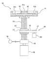
静圧支持機構90を備えた基板処理装置のより具体的な例について図3(a)および図3(b)を用いて説明する。図3(a)は静圧支持機構90を基板Wの下方に配置した基板処理装置の概念図である。静圧支持機構90には圧力流体1の流体供給路92が設けられ、圧力流体1が供給配管(図示せず)を経由して流体供給路92に供給されている。基板処理の際には、静圧支持機構90の支持ステージ91が基板Wに向かって上昇し、基板処理が終了すれば支持ステージ91は下降する。あるいは、基板Wの昇降機構を設けても良い。図3(a)に示す静圧支持機構90は、図1(a)に示す構造を有しているが、図1(b)または図1(c)に示す構造、あるいは別の構造であっても差し支えない。
図3(b)は静圧支持機構90を基板Wの上方に配置した基板処理装置の概念図である。基板処理装置の基本機能は図3(a)に示した例と同じである。
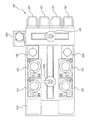
(3)実施例3
本発明の基板処理装置を用いて基板の表面処理を行う方法の実施例を説明する。基板、たとえばLSI製造途中の基板の片面を静圧支持機構90に向け、反対側の面を処理ヘッド50に向けて、本発明の基板処理装置に配置する。基板の周縁部をチャック11で保持し、デバイス面を静圧支持機構90で支持しながら、基板を回転させる。この状態で、基板の裏面(デバイスが形成されていない面)に処理ヘッド50を押し当てて裏面の傷やパーティクルなどの除去を行う。この際、チャック11での基板保持は処理中ずっと行わなくてもよい。
7 処理室
8 排気機構
9 排気ダクト
10 基板回転機構
11 チャック
12 中空モータ
14 静止部材
16 回転基台
18 ばね
20 アンギュラコンタクト玉軸受
21,22 磁気軸受
25 回転カバー
27 洗浄液供給ノズル/処理液供給ノズル
30 リフト機構
31 リングステージ
32 ロッド
33 エアシリンダ
35,36 気体軸受
39 タッチダウン軸受
40 クランプ
41 位置決め部
43,44,45 磁石
46 溝
47 突起部
50 スクラバー
51 スクラバーシャフト
53 揺動アーム
54 揺動軸
55 軸回転機構
56 スクラバー昇降機構
58 スクラバー回転機構
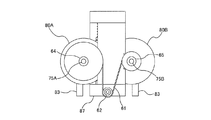
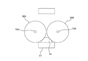
60 テープカートリッジ
61 洗浄テープ
62 押圧部材
63 付勢機構
64 テープ繰り出しリール
65 テープ巻き取りリール
67 テープ巻き取り軸
69,70 かさ歯車
71 エンドマーク検知センサ
72 チャック部
75A,75B リール軸
76A,76B 軸受
77 リールハウジング
78 ボールスプラインナット
79 ボールスプラインシャフト
80A,80B ブレーキ輪
81 ブレーキパッド
82 ばね
83 ピン
84A 繰り出しギヤ
84B 巻き取りギヤ
85A,85B ワンウェイクラッチ
86A,86B ラックギヤ
87 設置台
88 トルクリミッタ
90 静圧支持機構
91 支持ステージ
92 流体供給路
93 支持軸
95 ロータリジョイント
96 流体供給源
97 直動ガイド
98 ステージ昇降機構
99 ステージ回転機構
100 二流体ジェットノズル
101 回転アーム
102 揺動アーム
110 乾燥液供給ノズル
111 乾燥気体供給ノズル
120 ロードアンロード部
121 フロントロード部
123 第1の搬送ロボット
124 パーティクルカウンター
126 第2の搬送ロボット
127 基板処理装置
131,132 ウェハステーション
133 動作コントローラ
134 反転機構
Claims (35)
- 基板の第1の面の表面処理を行うスクラバーと、
前記第1の面とは反対側の前記基板の第2の面を流体圧により非接触に支持する基板支持面を有する静圧支持機構とを備え、
前記スクラバーは、その内部に前記第1の面に摺接させて前記第1の面の表面処理を行うテープ状の複数のスクラブ部材と、前記複数のスクラブ部材をそれぞれ繰り出す複数のテープ繰り出しリールと、前記複数のスクラブ部材をそれぞれ巻き取る複数のテープ巻き取りリールと、前記複数のテープ巻き取りリールがそれぞれ連結された複数のテープ巻き取り軸とを備え、
前記スクラバーは、該スクラバーの軸心周りに前記複数のスクラブ部材を回転させながら該複数のスクラブ部材を前記基板の第1の面に摺接させることを特徴とする基板処理装置。 - スクラブ部材を基板の第1の面に摺接させて該基板の表面処理を行うスクラバーと、
前記第1の面とは反対側の前記基板の第2の面を流体圧により非接触に支持する基板支持面を有する静圧支持機構とを備え、
前記スクラバーは、該スクラバーの軸心周りに前記スクラブ部材を回転させながら該スクラブ部材を前記基板の第1の面に摺接させるように構成され、
回転する前記スクラブ部材によって形成されるスクラブ面の直径は、前記基板の半径と同じか、または前記基板の半径よりも小さく、
前記基板支持面の直径は、前記基板の直径よりも小さく、
前記スクラブ面は、前記基板支持面と同心状であることを特徴とする基板処理装置。 - 前記スクラバーにより表面処理された前記基板を洗浄する洗浄部と、
洗浄された前記基板を乾燥させる乾燥部と、
内部に処理室が形成された隔壁をさらに備え、
前記スクラバー、前記洗浄部、および前記乾燥部は、前記処理室内に配置されていることを特徴とする請求項1または2に記載の基板処理装置。 - 前記複数のスクラブ部材、前記複数のテープ繰り出しリール、前記複数のテープ巻き取りリール、および前記複数のテープ巻き取り軸は、前記スクラバーの軸心周りに回転可能であることを特徴とする請求項1に記載の基板処理装置。
- 前記複数のテープ巻き取り軸を介して前記複数のテープ巻き取りリールを駆動する共通のモータをさらに備えたことを特徴とする請求項1に記載の基板処理装置。
- 前記乾燥部は、前記基板をその軸心を中心として回転させる基板回転機構から構成されていることを特徴とする請求項3に記載の基板処理装置。
- 前記基板回転機構は、前記基板を回転させる中空モータを備えており、前記基板回転機構はその中央部に空間を有する円筒形状を有しており、
前記静圧支持機構は、前記基板回転機構の前記空間内に配置されていることを特徴とする請求項3に記載の基板処理装置。 - 回転する前記複数のスクラブ部材によって形成されるスクラブ面と前記基板支持面は、同心状に配置されることを特徴とする請求項1に記載の基板処理装置。
- 前記スクラブ部材は、前記スクラバーの半径方向に延びる基板接触面を有することを特徴とする請求項1または2に記載の基板処理装置。
- 前記基板支持面には少なくとも1つの凹部が形成されており、
前記静圧支持機構は、前記基板支持面を有する支持ステージと、前記凹部に流体を供給するための流体供給路とを備えたことを特徴とする請求項1または2に記載の基板処理装置。 - 前記静圧支持機構は、前記基板支持面を有する支持ステージと、前記基板支持面上で開口する少なくとも1つの流体供給路とを備えたことを特徴とする請求項1または2に記載の基板処理装置。
- 前記静圧支持機構は、前記支持ステージを昇降させるステージ昇降機構をさらに有することを特徴する請求項10または11に記載の基板処理装置。
- 前記スクラバーは、前記複数のスクラブ部材を前記基板の第1の面に押し付ける複数の押圧部材をさらに備えることを特徴とする請求項1に記載の基板処理装置。
- 前記複数のスクラブ部材、前記複数の押圧部材、前記複数のテープ繰り出しリール、および前記複数のテープ巻き取りリールは、複数のテープカートリッジを構成し、該複数のテープカートリッジは前記スクラバーの内部に着脱可能に設置されていることを特徴とする請求項13に記載の基板処理装置。
- 前記スクラブ部材は、砥粒を有しない洗浄テープまたは砥粒を有する研磨テープであることを特徴とする請求項1または2に記載の基板処理装置。
- 前記第1の面はデバイスが形成されていない面であり、前記第2の面はデバイスが形成されている面であることを特徴とする請求項1または2に記載の基板処理装置。
- 前記第1の面はデバイスが形成されている面であり、前記第2の面はデバイスが形成されていない面であることを特徴とする請求項1または2に記載の基板処理装置。
- テープ状の複数のスクラブ部材を内部に有するスクラバーをその軸心周りに回転させ、前記複数のスクラブ部材を基板の第1の面に摺接させて該基板の表面処理を行う工程と、
前記表面処理がなされた前記基板を洗浄する工程と、
洗浄された前記基板を乾燥する工程とを含み、
前記スクラバーは、前記複数のスクラブ部材をそれぞれ繰り出す複数のテープ繰り出しリールと、前記複数のスクラブ部材をそれぞれ巻き取る複数のテープ巻き取りリールと、前記複数のテープ巻き取りリールがそれぞれ連結された複数のテープ巻き取り軸とを備え、
前記表面処理工程中、前記複数のスクラブ部材、前記複数のテープ繰り出しリール、前記複数のテープ巻き取りリール、および前記複数のテープ巻き取り軸は、前記スクラバーの軸心周りに回転し、
前記表面処理工程中に、前記第1の面とは反対側の前記基板の第2の面を流体圧により非接触に支持することを特徴とする基板処理方法。 - スクラブ部材を有するスクラバーをその軸心周りに回転させ、前記スクラブ部材を基板の第1の面に摺接させて該基板の表面処理を行う工程と、
前記表面処理がなされた前記基板を洗浄する工程と、
洗浄された前記基板を乾燥する工程とを含み、
前記表面処理工程中に、前記第1の面とは反対側の前記基板の第2の面と基板支持面との間を流れる流体の圧力により非接触に支持し、
回転する前記スクラブ部材によって形成されるスクラブ面の直径は、前記基板の半径と同じか、または前記基板の半径よりも小さく、
前記基板支持面の直径は、前記基板の直径よりも小さく、
前記スクラブ面は、前記基板支持面と同心状であることを特徴とする基板処理方法。 - 前記表面処理工程、前記洗浄工程、および前記乾燥工程を同一の処理室内で実施することを特徴とする請求項18または19に記載の基板処理方法。
- 前記洗浄工程中に、前記基板の第2の面を流体圧により非接触に支持することを特徴とする請求項18または19に記載の基板処理方法。
- 前記第1の面はデバイスが形成されていない面であり、前記第2の面はデバイスが形成されている面であることを特徴とする請求項18または19に記載の基板処理方法。
- 前記第1の面はデバイスが形成されている面であり、前記第2の面はデバイスが形成されていない面であることを特徴とする請求項18または19に記載の基板処理方法。
- 前記第1の面を構成する材料が、シリコン、シリコン化合物、ガリウム、ガリウム化合物、金属、金属化合物、および有機化合物のうちのいずれか1つであることを特徴とする請求項18または19に記載の基板処理方法。
- 前記スクラブ部材が、前記第1の面を構成する材料よりも軟質な材料、砥粒を含有する材料、および研磨テープから選ばれることを特徴とする請求項18または19に記載の基板処理方法。
- 前記表面処理工程は、前記第1の面に処理液を供給しながら前記スクラブ部材を前記第1の面に摺接させる工程であり、前記処理液の成分は、前記第1の面を構成する材料の溶解作用を持つ成分、砥粒、および前記スクラブ部材により除去された材料または反応生成物の再付着抑制成分の少なくとも一つを含むことを特徴とする請求項18または19に記載の基板処理方法。
- 前記砥粒の材質が、二酸化珪素、炭化珪素、窒化珪素、酸化アルミニウム、ダイヤモンドのいずれか1種またはその混合物であることを特徴とする請求項26に記載の基板処理方法。
- 前記処理液が中性またはアルカリ性であることを特徴とする請求項26に記載の基板処理方法。
- 前記処理液が酸性であることを特徴とする請求項26に記載の基板処理方法。
- 前記洗浄工程は、前記基板の第1の面に洗浄液を供給する工程と、前記基板の第1の面を接触式または非接触式手段で洗浄する工程とを含み、前記洗浄液は、所定のpHに制御した溶液、前記スクラブ部材により除去された材料の再付着防止成分を含む溶液、および純水のうち少なくとも1つを含むことを特徴とする請求項18または19に記載の基板処理方法。
- 前記洗浄液が中性またはアルカリ性であることを特徴とする請求項30に記載の基板処理方法。
- 前記洗浄液が酸性であることを特徴とする請求項30に記載の基板処理方法。
- 前記乾燥工程は、前記基板の高速回転、前記第1の面への気体噴出、または前記第1の面への低蒸気圧溶媒の供給のいずれかであることを特徴とする請求項18または19に記載の基板処理方法。
- 前記乾燥工程において、前記基板の周縁部に接触するチャックによって前記基板を保持することを特徴とする請求項18または19に記載の基板処理方法。
- 前記表面処理を行った後の前記第1の面の表面粗さが5μm以下であることを特徴とする請求項18または19に記載の基板処理方法。
Priority Applications (10)
| Application Number | Priority Date | Filing Date | Title |
|---|---|---|---|
| JP2012035365A JP6113960B2 (ja) | 2012-02-21 | 2012-02-21 | 基板処理装置および基板処理方法 |
| TW107101686A TWI669160B (zh) | 2012-02-21 | 2013-01-29 | 基板處理裝置 |
| TW102103272A TWI556881B (zh) | 2012-02-21 | 2013-01-29 | 基板處理裝置及基板處理方法 |
| TW105131269A TWI616239B (zh) | 2012-02-21 | 2013-01-29 | 擦洗器 |
| KR1020130015794A KR101922259B1 (ko) | 2012-02-21 | 2013-02-14 | 기판 처리 장치, 기판 처리 방법 및 스크러버 |
| US13/772,031 US10328465B2 (en) | 2012-02-21 | 2013-02-20 | Substrate processing apparatus and substrate processing method |
| JP2017051113A JP6334026B2 (ja) | 2012-02-21 | 2017-03-16 | スクラバー |
| KR1020180128710A KR101996763B1 (ko) | 2012-02-21 | 2018-10-26 | 기판 처리 장치, 기판 처리 방법 및 스크러버 |
| US16/405,559 US10799917B2 (en) | 2012-02-21 | 2019-05-07 | Substrate processing apparatus and substrate processing method |
| US16/405,631 US11192147B2 (en) | 2012-02-21 | 2019-05-07 | Substrate processing apparatus and substrate processing method |
Applications Claiming Priority (1)
| Application Number | Priority Date | Filing Date | Title |
|---|---|---|---|
| JP2012035365A JP6113960B2 (ja) | 2012-02-21 | 2012-02-21 | 基板処理装置および基板処理方法 |
Related Child Applications (1)
| Application Number | Title | Priority Date | Filing Date |
|---|---|---|---|
| JP2017051113A Division JP6334026B2 (ja) | 2012-02-21 | 2017-03-16 | スクラバー |
Publications (3)
| Publication Number | Publication Date |
|---|---|
| JP2013172019A JP2013172019A (ja) | 2013-09-02 |
| JP2013172019A5 JP2013172019A5 (ja) | 2015-04-02 |
| JP6113960B2 true JP6113960B2 (ja) | 2017-04-12 |
Family
ID=48981329
Family Applications (2)
| Application Number | Title | Priority Date | Filing Date |
|---|---|---|---|
| JP2012035365A Active JP6113960B2 (ja) | 2012-02-21 | 2012-02-21 | 基板処理装置および基板処理方法 |
| JP2017051113A Active JP6334026B2 (ja) | 2012-02-21 | 2017-03-16 | スクラバー |
Family Applications After (1)
| Application Number | Title | Priority Date | Filing Date |
|---|---|---|---|
| JP2017051113A Active JP6334026B2 (ja) | 2012-02-21 | 2017-03-16 | スクラバー |
Country Status (4)
| Country | Link |
|---|---|
| US (3) | US10328465B2 (ja) |
| JP (2) | JP6113960B2 (ja) |
| KR (2) | KR101922259B1 (ja) |
| TW (3) | TWI616239B (ja) |
Cited By (1)
| Publication number | Priority date | Publication date | Assignee | Title |
|---|---|---|---|---|
| CN110624893A (zh) * | 2019-09-25 | 2019-12-31 | 上海华力集成电路制造有限公司 | 一种兆声波组合气体喷雾清洗装置及其应用 |
Families Citing this family (33)
| Publication number | Priority date | Publication date | Assignee | Title |
|---|---|---|---|---|
| DE102008041250A1 (de) * | 2008-08-13 | 2010-02-25 | Ers Electronic Gmbh | Verfahren und Vorrichtung zum thermischen Bearbeiten von Kunststoffscheiben, insbesondere Moldwafern |
| US20130217228A1 (en) | 2012-02-21 | 2013-08-22 | Masako Kodera | Method for fabricating semiconductor device |
| JP6113960B2 (ja) * | 2012-02-21 | 2017-04-12 | 株式会社荏原製作所 | 基板処理装置および基板処理方法 |
| JP6100002B2 (ja) | 2013-02-01 | 2017-03-22 | 株式会社荏原製作所 | 基板裏面の研磨方法および基板処理装置 |
| JP2014220495A (ja) * | 2013-04-12 | 2014-11-20 | レーザーテック株式会社 | 異物除去装置 |
| JP6145334B2 (ja) | 2013-06-28 | 2017-06-07 | 株式会社荏原製作所 | 基板処理装置 |
| US9947572B2 (en) | 2014-03-26 | 2018-04-17 | SCREEN Holdings Co., Ltd. | Substrate processing apparatus |
| JP6312534B2 (ja) | 2014-06-10 | 2018-04-18 | 株式会社荏原製作所 | 基板洗浄装置 |
| CN107148665B (zh) | 2014-10-31 | 2018-04-20 | 株式会社荏原制作所 | 基板清洗装置及基板清洗方法 |
| JP6554864B2 (ja) * | 2015-03-30 | 2019-08-07 | 大日本印刷株式会社 | ペリクル接着剤除去装置及びペリクル接着剤除去方法 |
| US10276365B2 (en) | 2016-02-01 | 2019-04-30 | SCREEN Holdings Co., Ltd. | Substrate cleaning device, substrate processing apparatus, substrate cleaning method and substrate processing method |
| JP6726575B2 (ja) * | 2016-02-01 | 2020-07-22 | 株式会社Screenホールディングス | 基板洗浄装置、基板処理装置、基板洗浄方法および基板処理方法 |
| JP7052280B2 (ja) * | 2016-11-29 | 2022-04-12 | 東京エレクトロン株式会社 | 基板処理装置、基板処理方法及び記憶媒体 |
| JP6882017B2 (ja) * | 2017-03-06 | 2021-06-02 | 株式会社荏原製作所 | 研磨方法、研磨装置、および基板処理システム |
| JP6836432B2 (ja) * | 2017-03-22 | 2021-03-03 | 株式会社荏原製作所 | 基板処理装置および基板処理方法 |
| JP6920849B2 (ja) * | 2017-03-27 | 2021-08-18 | 株式会社荏原製作所 | 基板処理方法および装置 |
| JP6873782B2 (ja) * | 2017-03-29 | 2021-05-19 | 株式会社荏原製作所 | 研磨装置、研磨方法、およびプログラムを記録したコンピュータ読み取り可能な記録媒体 |
| JP6779173B2 (ja) * | 2017-05-18 | 2020-11-04 | 株式会社荏原製作所 | 基板処理装置、プログラムを記録した記録媒体 |
| JP6908496B2 (ja) * | 2017-10-25 | 2021-07-28 | 株式会社荏原製作所 | 研磨装置 |
| JP6974116B2 (ja) * | 2017-10-27 | 2021-12-01 | 株式会社荏原製作所 | 基板保持装置並びに基板保持装置を備えた基板処理装置および基板処理方法 |
| JP2019091746A (ja) * | 2017-11-13 | 2019-06-13 | 株式会社荏原製作所 | 基板の表面を処理する装置および方法 |
| JP6887371B2 (ja) * | 2017-12-20 | 2021-06-16 | 株式会社荏原製作所 | 基板処理装置、基板処理装置の制御方法、プログラムを格納した記憶媒体 |
| JP7020986B2 (ja) * | 2018-04-16 | 2022-02-16 | 株式会社荏原製作所 | 基板処理装置および基板保持装置 |
| CN108656721B (zh) * | 2018-05-24 | 2023-10-13 | 中策橡胶集团股份有限公司 | 一种反光带热转印贴合设备 |
| KR102570220B1 (ko) * | 2018-05-29 | 2023-08-25 | 주식회사 케이씨텍 | 기판 처리 장치 |
| JP2019216207A (ja) * | 2018-06-14 | 2019-12-19 | 株式会社荏原製作所 | 基板処理方法 |
| JP7037459B2 (ja) * | 2018-09-10 | 2022-03-16 | キオクシア株式会社 | 半導体製造装置および半導体装置の製造方法 |
| JP7145019B2 (ja) * | 2018-09-19 | 2022-09-30 | 株式会社Screenホールディングス | レシピ変換方法、レシピ変換プログラム、レシピ変換装置および基板処理システム |
| JP6979935B2 (ja) * | 2018-10-24 | 2021-12-15 | 三菱電機株式会社 | 半導体製造装置および半導体製造方法 |
| CN110332616B (zh) * | 2019-06-20 | 2023-10-20 | 宁波奥克斯电气股份有限公司 | 一种空调器室内机自清洁装置及其控制方法 |
| CN112946957B (zh) * | 2019-11-26 | 2023-06-02 | 上海微电子装备(集团)股份有限公司 | 光配向装置、双台光配向装置、光配向方法及光配向系统 |
| KR102396431B1 (ko) * | 2020-08-14 | 2022-05-10 | 피에스케이 주식회사 | 기판 처리 장치 및 기판 반송 방법 |
| JP2022174633A (ja) * | 2021-05-11 | 2022-11-24 | 東京エレクトロン株式会社 | 基板処理装置および基板処理方法 |
Family Cites Families (57)
| Publication number | Priority date | Publication date | Assignee | Title |
|---|---|---|---|---|
| US2761255A (en) * | 1953-10-02 | 1956-09-04 | Thompson Prod Inc | Polishing machine |
| JPS61136764A (ja) * | 1984-12-04 | 1986-06-24 | Fuji Photo Film Co Ltd | 磁気デイスクのバ−ニツシユ方法およびその装置 |
| JPS61203643A (ja) * | 1985-03-07 | 1986-09-09 | Mitsubishi Electric Corp | 洗浄装置 |
| JPH0695508B2 (ja) * | 1986-11-28 | 1994-11-24 | 大日本スクリ−ン製造株式会社 | 基板の両面洗浄装置 |
| JPS63251166A (ja) * | 1987-04-07 | 1988-10-18 | Hitachi Ltd | ウエハチヤツク |
| JPH04363022A (ja) * | 1991-06-06 | 1992-12-15 | Enya Syst:Kk | 貼付板洗浄装置 |
| KR100273032B1 (en) * | 1992-07-30 | 2000-12-01 | Hitachi Maxell | Tape cartridge |
| US5485644A (en) | 1993-03-18 | 1996-01-23 | Dainippon Screen Mfg. Co., Ltd. | Substrate treating apparatus |
| US5664987A (en) * | 1994-01-31 | 1997-09-09 | National Semiconductor Corporation | Methods and apparatus for control of polishing pad conditioning for wafer planarization |
| JPH08264626A (ja) | 1994-04-28 | 1996-10-11 | Hitachi Ltd | 試料保持方法及び試料表面の流体処理方法並びにそれらの装置 |
| DE69512971T2 (de) * | 1994-08-09 | 2000-05-18 | Ontrak Systems Inc | Linear Poliergerät und Wafer Planarisierungsverfahren |
| TW348279B (en) * | 1995-04-10 | 1998-12-21 | Matsushita Electric Ind Co Ltd | Substrate grinding method |
| JP2758152B2 (ja) * | 1995-04-10 | 1998-05-28 | 松下電器産業株式会社 | 被研磨基板の保持装置及び基板の研磨方法 |
| JP3447869B2 (ja) | 1995-09-20 | 2003-09-16 | 株式会社荏原製作所 | 洗浄方法及び装置 |
| JP3138205B2 (ja) * | 1996-03-27 | 2001-02-26 | 株式会社不二越 | 高脆性材の両面研削装置 |
| JP2921499B2 (ja) | 1996-07-30 | 1999-07-19 | 日本電気株式会社 | プラズマ処理装置 |
| JPH10189511A (ja) * | 1996-12-20 | 1998-07-21 | Sony Corp | ウェーハ洗浄装置 |
| US5868857A (en) * | 1996-12-30 | 1999-02-09 | Intel Corporation | Rotating belt wafer edge cleaning apparatus |
| JP3630524B2 (ja) * | 1997-05-08 | 2005-03-16 | 大日本スクリーン製造株式会社 | 基板洗浄装置 |
| US6062959A (en) * | 1997-11-05 | 2000-05-16 | Aplex Group | Polishing system including a hydrostatic fluid bearing support |
| JP3654779B2 (ja) * | 1998-01-06 | 2005-06-02 | 東京エレクトロン株式会社 | 基板洗浄具及び基板洗浄方法 |
| US20030007666A1 (en) * | 1998-04-13 | 2003-01-09 | Stewartson James A. | Method and apparatus for relief texture map flipping |
| US6875085B2 (en) * | 1998-11-06 | 2005-04-05 | Mosel Vitelic, Inc. | Polishing system including a hydrostatic fluid bearing support |
| JP2000176386A (ja) * | 1998-12-16 | 2000-06-27 | Ebara Corp | 基板洗浄装置 |
| US6076686A (en) * | 1999-01-04 | 2000-06-20 | Advanced Micro Devices, Inc. | Support structure for use during package removal from a multi-layer integrated circuit device |
| US6269510B1 (en) * | 1999-01-04 | 2001-08-07 | International Business Machines Corporation | Post CMP clean brush with torque monitor |
| JP2000296368A (ja) * | 1999-04-13 | 2000-10-24 | Seiko Epson Corp | 洗浄装置 |
| AU5295900A (en) * | 1999-05-27 | 2000-12-18 | Lam Research Corporation | Disk cascade scrubber |
| US6197182B1 (en) * | 1999-07-07 | 2001-03-06 | Technic Inc. | Apparatus and method for plating wafers, substrates and other articles |
| JP4156200B2 (ja) * | 2001-01-09 | 2008-09-24 | 株式会社荏原製作所 | 研磨装置及び研磨方法 |
| JP2003007666A (ja) * | 2001-06-27 | 2003-01-10 | Ebara Corp | 基板洗浄装置 |
| TWI275436B (en) * | 2002-01-31 | 2007-03-11 | Ebara Corp | Electrochemical machining device, and substrate processing apparatus and method |
| JP4090247B2 (ja) * | 2002-02-12 | 2008-05-28 | 株式会社荏原製作所 | 基板処理装置 |
| KR100954534B1 (ko) * | 2002-10-09 | 2010-04-23 | 고요 기카이 고교 가부시키가이샤 | 얇은 원판형상 공작물의 양면 연삭방법 및 양면 연삭장치 |
| JP2006013107A (ja) * | 2004-06-25 | 2006-01-12 | Dainippon Screen Mfg Co Ltd | 基板処理装置 |
| US8211242B2 (en) | 2005-02-07 | 2012-07-03 | Ebara Corporation | Substrate processing method, substrate processing apparatus, and control program |
| JP2006245022A (ja) * | 2005-02-28 | 2006-09-14 | Dainippon Screen Mfg Co Ltd | 基板処理装置 |
| WO2006112532A1 (en) * | 2005-04-19 | 2006-10-26 | Ebara Corporation | Substrate processing apparatus |
| JP2007157898A (ja) * | 2005-12-02 | 2007-06-21 | Tokyo Electron Ltd | 基板洗浄方法、基板洗浄装置、制御プログラム、およびコンピュータ読取可能な記憶媒体 |
| US7997289B1 (en) * | 2006-10-03 | 2011-08-16 | Xyratex Technology Limited | Methods of and apparatus for cleaning and conveying a substrate |
| JP4999417B2 (ja) * | 2006-10-04 | 2012-08-15 | 株式会社荏原製作所 | 研磨装置、研磨方法、処理装置 |
| JP2008290233A (ja) * | 2007-05-21 | 2008-12-04 | Applied Materials Inc | 半導体製造における基板斜面及び縁部の研磨用の高性能及び低価格の研磨テープのための方法及び装置 |
| JP5242242B2 (ja) * | 2007-10-17 | 2013-07-24 | 株式会社荏原製作所 | 基板洗浄装置 |
| US20090264053A1 (en) * | 2008-04-21 | 2009-10-22 | Applied Materials, Inc. | Apparatus and methods for using a polishing tape cassette |
| JP5211835B2 (ja) * | 2008-04-30 | 2013-06-12 | ソニー株式会社 | ウエハ研磨装置およびウエハ研磨方法 |
| JP2010080477A (ja) * | 2008-09-24 | 2010-04-08 | Toshiba Corp | 微細パターン基材の洗浄方法 |
| JP2010087338A (ja) * | 2008-10-01 | 2010-04-15 | Panasonic Corp | 半導体装置の製造方法および半導体製造装置 |
| JP5463570B2 (ja) * | 2008-10-31 | 2014-04-09 | Sumco Techxiv株式会社 | ウェハ用両頭研削装置および両頭研削方法 |
| JP2010278103A (ja) * | 2009-05-27 | 2010-12-09 | Sumitomo Metal Mining Co Ltd | スクラブ洗浄装置 |
| JP5663295B2 (ja) * | 2010-01-15 | 2015-02-04 | 株式会社荏原製作所 | 研磨装置、研磨方法、研磨具を押圧する押圧部材 |
| JP2012028697A (ja) | 2010-07-27 | 2012-02-09 | Toshiba Corp | 洗浄装置、方法 |
| US20120111360A1 (en) * | 2010-11-10 | 2012-05-10 | Helmuth Treichel | Method and Apparatus for Cleaning a Substrate |
| US8540551B2 (en) * | 2010-12-15 | 2013-09-24 | Corning Incorporated | Glass edge finish system, belt assembly, and method for using same |
| US20130217228A1 (en) * | 2012-02-21 | 2013-08-22 | Masako Kodera | Method for fabricating semiconductor device |
| JP6113960B2 (ja) | 2012-02-21 | 2017-04-12 | 株式会社荏原製作所 | 基板処理装置および基板処理方法 |
| JP6145334B2 (ja) * | 2013-06-28 | 2017-06-07 | 株式会社荏原製作所 | 基板処理装置 |
| JP6882017B2 (ja) * | 2017-03-06 | 2021-06-02 | 株式会社荏原製作所 | 研磨方法、研磨装置、および基板処理システム |
-
2012
- 2012-02-21 JP JP2012035365A patent/JP6113960B2/ja active Active
-
2013
- 2013-01-29 TW TW105131269A patent/TWI616239B/zh active
- 2013-01-29 TW TW107101686A patent/TWI669160B/zh active
- 2013-01-29 TW TW102103272A patent/TWI556881B/zh active
- 2013-02-14 KR KR1020130015794A patent/KR101922259B1/ko active IP Right Grant
- 2013-02-20 US US13/772,031 patent/US10328465B2/en active Active
-
2017
- 2017-03-16 JP JP2017051113A patent/JP6334026B2/ja active Active
-
2018
- 2018-10-26 KR KR1020180128710A patent/KR101996763B1/ko active IP Right Grant
-
2019
- 2019-05-07 US US16/405,559 patent/US10799917B2/en active Active
- 2019-05-07 US US16/405,631 patent/US11192147B2/en active Active
Cited By (2)
| Publication number | Priority date | Publication date | Assignee | Title |
|---|---|---|---|---|
| CN110624893A (zh) * | 2019-09-25 | 2019-12-31 | 上海华力集成电路制造有限公司 | 一种兆声波组合气体喷雾清洗装置及其应用 |
| CN110624893B (zh) * | 2019-09-25 | 2022-06-14 | 上海华力集成电路制造有限公司 | 一种兆声波组合气体喷雾清洗装置及其应用 |
Also Published As
| Publication number | Publication date |
|---|---|
| TW201345621A (zh) | 2013-11-16 |
| JP2013172019A (ja) | 2013-09-02 |
| US20130213437A1 (en) | 2013-08-22 |
| JP6334026B2 (ja) | 2018-05-30 |
| KR20130096185A (ko) | 2013-08-29 |
| KR101996763B1 (ko) | 2019-07-04 |
| TWI616239B (zh) | 2018-03-01 |
| US10328465B2 (en) | 2019-06-25 |
| TWI556881B (zh) | 2016-11-11 |
| TW201811454A (zh) | 2018-04-01 |
| TWI669160B (zh) | 2019-08-21 |
| US11192147B2 (en) | 2021-12-07 |
| TW201703880A (zh) | 2017-02-01 |
| KR101922259B1 (ko) | 2018-11-26 |
| JP2017118146A (ja) | 2017-06-29 |
| US20190262869A1 (en) | 2019-08-29 |
| US20190262870A1 (en) | 2019-08-29 |
| KR20180121438A (ko) | 2018-11-07 |
| US10799917B2 (en) | 2020-10-13 |
Similar Documents
| Publication | Publication Date | Title |
|---|---|---|
| JP6334026B2 (ja) | スクラバー | |
| JP6568975B2 (ja) | テープカートリッジ、スクラバー、および基板処理装置 | |
| TWI525686B (zh) | 基板洗淨方法 | |
| US20140242885A1 (en) | Polishing apparatus and polishing method | |
| JP6882017B2 (ja) | 研磨方法、研磨装置、および基板処理システム | |
| JP6054805B2 (ja) | 基板洗浄装置 | |
| US20130185884A1 (en) | Cleaning module and process for particle reduction | |
| CN110610848A (zh) | 基板处理方法 | |
| JP4451429B2 (ja) | 洗浄装置 | |
| US20190184517A1 (en) | Substrate processing apparatus, substrate processing method, and storage medium storing program | |
| JP4963411B2 (ja) | 半導体装置または半導体ウェハの製造方法 | |
| JP6625461B2 (ja) | 研磨装置 | |
| JP2021130145A (ja) | 研磨装置および研磨方法 | |
| TW201934209A (zh) | 清洗裝置、清洗方法及電腦記錄媒體 | |
| WO2022260128A1 (ja) | 基板処理システム、及び基板処理方法 | |
| JP2023105856A (ja) | 基板洗浄方法、基板洗浄装置、基板洗浄部材、及び、基板洗浄部材の製造方法 | |
| TW201842983A (zh) | 清洗基板裏面的裝置及方法 |
Legal Events
| Date | Code | Title | Description |
|---|---|---|---|
| A521 | Request for written amendment filed |
Free format text: JAPANESE INTERMEDIATE CODE: A523 Effective date: 20150213 |
|
| A621 | Written request for application examination |
Free format text: JAPANESE INTERMEDIATE CODE: A621 Effective date: 20150213 |
|
| A131 | Notification of reasons for refusal |
Free format text: JAPANESE INTERMEDIATE CODE: A131 Effective date: 20160315 |
|
| A977 | Report on retrieval |
Free format text: JAPANESE INTERMEDIATE CODE: A971007 Effective date: 20160316 |
|
| A521 | Request for written amendment filed |
Free format text: JAPANESE INTERMEDIATE CODE: A523 Effective date: 20160513 |
|
| A131 | Notification of reasons for refusal |
Free format text: JAPANESE INTERMEDIATE CODE: A131 Effective date: 20160913 |
|
| A521 | Request for written amendment filed |
Free format text: JAPANESE INTERMEDIATE CODE: A523 Effective date: 20161114 |
|
| TRDD | Decision of grant or rejection written | ||
| A01 | Written decision to grant a patent or to grant a registration (utility model) |
Free format text: JAPANESE INTERMEDIATE CODE: A01 Effective date: 20170214 |
|
| A61 | First payment of annual fees (during grant procedure) |
Free format text: JAPANESE INTERMEDIATE CODE: A61 Effective date: 20170316 |
|
| R150 | Certificate of patent or registration of utility model |
Ref document number: 6113960 Country of ref document: JP Free format text: JAPANESE INTERMEDIATE CODE: R150 |
|
| S111 | Request for change of ownership or part of ownership |
Free format text: JAPANESE INTERMEDIATE CODE: R313115 |
|
| R350 | Written notification of registration of transfer |
Free format text: JAPANESE INTERMEDIATE CODE: R350 |
|
| R250 | Receipt of annual fees |
Free format text: JAPANESE INTERMEDIATE CODE: R250 |
|
| R250 | Receipt of annual fees |
Free format text: JAPANESE INTERMEDIATE CODE: R250 |
|
| S111 | Request for change of ownership or part of ownership |
Free format text: JAPANESE INTERMEDIATE CODE: R313115 |
|
| R250 | Receipt of annual fees |
Free format text: JAPANESE INTERMEDIATE CODE: R250 |
|
| R350 | Written notification of registration of transfer |
Free format text: JAPANESE INTERMEDIATE CODE: R350 |
|
| R250 | Receipt of annual fees |
Free format text: JAPANESE INTERMEDIATE CODE: R250 |
|
| R250 | Receipt of annual fees |
Free format text: JAPANESE INTERMEDIATE CODE: R250 |