JP5985201B2 - 発光装置および照明装置 - Google Patents
発光装置および照明装置 Download PDFInfo
- Publication number
- JP5985201B2 JP5985201B2 JP2012034517A JP2012034517A JP5985201B2 JP 5985201 B2 JP5985201 B2 JP 5985201B2 JP 2012034517 A JP2012034517 A JP 2012034517A JP 2012034517 A JP2012034517 A JP 2012034517A JP 5985201 B2 JP5985201 B2 JP 5985201B2
- Authority
- JP
- Japan
- Prior art keywords
- layer
- electrode
- light emitting
- emitting device
- insulating substrate
- Prior art date
- Legal status (The legal status is an assumption and is not a legal conclusion. Google has not performed a legal analysis and makes no representation as to the accuracy of the status listed.)
- Expired - Fee Related
Links
Images


Classifications
-
- H—ELECTRICITY
- H01—ELECTRIC ELEMENTS
- H01L—SEMICONDUCTOR DEVICES NOT COVERED BY CLASS H10
- H01L33/00—Semiconductor devices with at least one potential-jump barrier or surface barrier specially adapted for light emission; Processes or apparatus specially adapted for the manufacture or treatment thereof or of parts thereof; Details thereof
- H01L33/36—Semiconductor devices with at least one potential-jump barrier or surface barrier specially adapted for light emission; Processes or apparatus specially adapted for the manufacture or treatment thereof or of parts thereof; Details thereof characterised by the electrodes
- H01L33/40—Materials therefor
-
- H—ELECTRICITY
- H01—ELECTRIC ELEMENTS
- H01L—SEMICONDUCTOR DEVICES NOT COVERED BY CLASS H10
- H01L33/00—Semiconductor devices with at least one potential-jump barrier or surface barrier specially adapted for light emission; Processes or apparatus specially adapted for the manufacture or treatment thereof or of parts thereof; Details thereof
- H01L33/48—Semiconductor devices with at least one potential-jump barrier or surface barrier specially adapted for light emission; Processes or apparatus specially adapted for the manufacture or treatment thereof or of parts thereof; Details thereof characterised by the semiconductor body packages
- H01L33/62—Arrangements for conducting electric current to or from the semiconductor body, e.g. lead-frames, wire-bonds or solder balls
-
- H—ELECTRICITY
- H01—ELECTRIC ELEMENTS
- H01L—SEMICONDUCTOR DEVICES NOT COVERED BY CLASS H10
- H01L25/00—Assemblies consisting of a plurality of individual semiconductor or other solid state devices ; Multistep manufacturing processes thereof
- H01L25/03—Assemblies consisting of a plurality of individual semiconductor or other solid state devices ; Multistep manufacturing processes thereof all the devices being of a type provided for in the same subgroup of groups H01L27/00 - H01L33/00, or in a single subclass of H10K, H10N, e.g. assemblies of rectifier diodes
- H01L25/04—Assemblies consisting of a plurality of individual semiconductor or other solid state devices ; Multistep manufacturing processes thereof all the devices being of a type provided for in the same subgroup of groups H01L27/00 - H01L33/00, or in a single subclass of H10K, H10N, e.g. assemblies of rectifier diodes the devices not having separate containers
- H01L25/075—Assemblies consisting of a plurality of individual semiconductor or other solid state devices ; Multistep manufacturing processes thereof all the devices being of a type provided for in the same subgroup of groups H01L27/00 - H01L33/00, or in a single subclass of H10K, H10N, e.g. assemblies of rectifier diodes the devices not having separate containers the devices being of a type provided for in group H01L33/00
- H01L25/0753—Assemblies consisting of a plurality of individual semiconductor or other solid state devices ; Multistep manufacturing processes thereof all the devices being of a type provided for in the same subgroup of groups H01L27/00 - H01L33/00, or in a single subclass of H10K, H10N, e.g. assemblies of rectifier diodes the devices not having separate containers the devices being of a type provided for in group H01L33/00 the devices being arranged next to each other
-
- H—ELECTRICITY
- H01—ELECTRIC ELEMENTS
- H01L—SEMICONDUCTOR DEVICES NOT COVERED BY CLASS H10
- H01L2924/00—Indexing scheme for arrangements or methods for connecting or disconnecting semiconductor or solid-state bodies as covered by H01L24/00
- H01L2924/0001—Technical content checked by a classifier
- H01L2924/0002—Not covered by any one of groups H01L24/00, H01L24/00 and H01L2224/00
-
- H—ELECTRICITY
- H01—ELECTRIC ELEMENTS
- H01L—SEMICONDUCTOR DEVICES NOT COVERED BY CLASS H10
- H01L2933/00—Details relating to devices covered by the group H01L33/00 but not provided for in its subgroups
- H01L2933/0008—Processes
- H01L2933/0016—Processes relating to electrodes
Description
本発明に係る一実施形態について、図1〜図5を参照して以下に説明する。
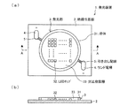
図1(a)は、本実施形態に係る発光装置1の構成を示す平面図であり、図1(a)は図1(b)のA−A線矢視断面図である。
図2は、LEDチップ32の接続構成を示す回路図である。
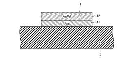
図3は、発光装置1におけるランド電極4および引き出し配線5の形成部分を拡大して示す縦断面図である。図4は、ランド電極4の構造を示す縦断面図である。図5は、ランド電極4の他の構造を示す縦断面図である。
続いて、ランド電極4の作製手順について説明する。
以上のように、発光装置1において、ランド電極4は、少なくとも、表面を含む一部が、AuおよびAgより高硬度であり、かつ使用電流域でランド電極4の導通が確保できる程度の硫化耐性を有する導電材料によって形成されている。これにより、ランド電極4が前述のコネクタの端子と接触することにより電気的接続が保持されている状態で振動しても、従来のAuやAgによって形成された電極と比較して、損傷を受けにくくなる。特に、電極材料のビッカース硬さが100Hv以上であることにより、上記のような損傷をほとんど受けなくなる。また、ランド電極4が、使用電流域でランド電極4の導通が確保できる程度の硫化耐性を有する導電材料で形成されるので、硫黄成分ガスによってランド電極4の表面に硫化膜が形成されても、ランド電極4が導通しなくなるという不都合は生じない。このように、ランド電極4の強度および耐食性が従来の電極と比べて優れているので、発光装置1の信頼性を向上させることができる。
本発明に係る他の実施形態について、図6〜図7を参照して以下に説明する。
図6は、発光装置1を備えるLED電球11の構成を示す縦断面図である。図7は、LED電球11における発光装置1の実装部分の構成を示す上面図である。
上記のように構成されるLED電球11は、実施形態1で説明したように形成されるランド電極4を備えた発光装置1を光源として実装している。
本発明は上述した実施形態に限定されるものではなく、請求項に示した範囲で種々の変更が可能である。すなわち、請求項に示した範囲で適宜変更した技術的手段を組み合わせて得られる実施形態についても本発明の技術的範囲に含まれる。
2 絶縁性基板
3 発光部
4 ランド電極(電極)
5 引き出し配線
11 LED電球(照明装置)
32 LEDチップ(半導体発光素子)
41 第1層
42 第2層
Claims (10)
- 絶縁性基板上に、半導体発光素子が実装されるとともに、当該半導体発光素子への給電のための電極が形成されている発光装置において、
前記電極は、前記絶縁性基板上に形成される第1層と、当該第1層上に形成される第2層とを含み、
前記第1層は、前記絶縁性基板上に形成された引き出し配線と一体に低抵抗の導電材料によって形成され、
前記第2層は、前記第1層より高硬度であり、かつ使用電流域で前記電極の導通が確保できる程度の硫化耐性を有するとともに、30%以上かつ80%以下の重量比でPdを含有しているAgPdによって形成されており、
前記第2層は、前記第1層が露出している部分を覆うことで外気から遮断し、
前記引き出し配線は外気に晒されていることを特徴とする発光装置。 - 前記AgPdのビッカース硬さが100Hv以上であることを特徴とする請求項1に記載の発光装置。
- 前記電極は印刷によって形成されていることを特徴とする請求項1または2に記載の発光装置。
- 前記電極は、複数設けられており、少なくとも一対が印刷によって形成されていることを特徴とする請求項3に記載の発光装置。
- 前記第1層がAgによって形成されていることを特徴とする請求項1に記載の発光装置。
- 前記第2層が30%以上かつ40%以下の重量比でPdを含有しているAgPdによって形成されていることを特徴とする請求項5に記載の発光装置。
- 前記第2層は2μm以上かつ8μm以下の厚さに形成されていることを特徴とする請求項5または6に記載の発光装置。
- 前記絶縁性基板は、前記半導体発光素子が実装されるとともに前記電極が形成される表面のうち、少なくとも前記電極が形成される領域が絶縁性を有していることを特徴とする請求項1に記載の発光装置。
- 前記絶縁性基板は、少なくとも前記表面の全体が絶縁性を有していることを特徴とする請求項8に記載の発光装置。
- 請求項1から9のいずれか1項に記載の発光装置を光源として備えていることを特徴とする照明装置。
Priority Applications (5)
| Application Number | Priority Date | Filing Date | Title |
|---|---|---|---|
| JP2012034517A JP5985201B2 (ja) | 2012-02-20 | 2012-02-20 | 発光装置および照明装置 |
| US14/376,578 US9577153B2 (en) | 2012-02-20 | 2013-02-19 | Light emission device and illumination device |
| EP13751422.0A EP2819191A4 (en) | 2012-02-20 | 2013-02-19 | LIGHT EMITTING DEVICE AND LIGHTING DEVICE |
| PCT/JP2013/054045 WO2013125539A1 (ja) | 2012-02-20 | 2013-02-19 | 発光装置および照明装置 |
| CN201380007510.5A CN104081548B (zh) | 2012-02-20 | 2013-02-19 | 发光装置以及照明装置 |
Applications Claiming Priority (1)
| Application Number | Priority Date | Filing Date | Title |
|---|---|---|---|
| JP2012034517A JP5985201B2 (ja) | 2012-02-20 | 2012-02-20 | 発光装置および照明装置 |
Related Child Applications (1)
| Application Number | Title | Priority Date | Filing Date |
|---|---|---|---|
| JP2015246758A Division JP6411320B2 (ja) | 2015-12-17 | 2015-12-17 | 発光装置および照明装置 |
Publications (3)
| Publication Number | Publication Date |
|---|---|
| JP2013171952A JP2013171952A (ja) | 2013-09-02 |
| JP2013171952A5 JP2013171952A5 (ja) | 2014-10-16 |
| JP5985201B2 true JP5985201B2 (ja) | 2016-09-06 |
Family
ID=49005724
Family Applications (1)
| Application Number | Title | Priority Date | Filing Date |
|---|---|---|---|
| JP2012034517A Expired - Fee Related JP5985201B2 (ja) | 2012-02-20 | 2012-02-20 | 発光装置および照明装置 |
Country Status (5)
| Country | Link |
|---|---|
| US (1) | US9577153B2 (ja) |
| EP (1) | EP2819191A4 (ja) |
| JP (1) | JP5985201B2 (ja) |
| CN (1) | CN104081548B (ja) |
| WO (1) | WO2013125539A1 (ja) |
Families Citing this family (8)
| Publication number | Priority date | Publication date | Assignee | Title |
|---|---|---|---|---|
| USD791089S1 (en) * | 2015-10-23 | 2017-07-04 | Citizen Electronics Co., Ltd. | Light-emitting diode |
| JP6520663B2 (ja) * | 2015-11-27 | 2019-05-29 | 日亜化学工業株式会社 | 素子載置用基板及び発光装置 |
| EP3491679B1 (en) | 2016-07-26 | 2023-02-22 | CreeLED, Inc. | Light emitting diodes, components and related methods |
| US11024785B2 (en) * | 2018-05-25 | 2021-06-01 | Creeled, Inc. | Light-emitting diode packages |
| US11335833B2 (en) | 2018-08-31 | 2022-05-17 | Creeled, Inc. | Light-emitting diodes, light-emitting diode arrays and related devices |
| USD902448S1 (en) | 2018-08-31 | 2020-11-17 | Cree, Inc. | Light emitting diode package |
| US11233183B2 (en) | 2018-08-31 | 2022-01-25 | Creeled, Inc. | Light-emitting diodes, light-emitting diode arrays and related devices |
| US11101411B2 (en) | 2019-06-26 | 2021-08-24 | Creeled, Inc. | Solid-state light emitting devices including light emitting diodes in package structures |
Family Cites Families (25)
| Publication number | Priority date | Publication date | Assignee | Title |
|---|---|---|---|---|
| JPH0419571Y2 (ja) * | 1986-04-02 | 1992-05-01 | ||
| JPH05243240A (ja) | 1992-02-28 | 1993-09-21 | Nec Corp | 熱処理装置 |
| JPH05243420A (ja) * | 1992-02-28 | 1993-09-21 | Nippondenso Co Ltd | 厚膜回路基板およびこれを用いた半導体装置 |
| JP2797951B2 (ja) | 1994-02-22 | 1998-09-17 | 住友金属工業株式会社 | 銀−パラジウム合金めっき方法およびめっき浴 |
| JP3164276B2 (ja) | 1995-08-02 | 2001-05-08 | スズキ株式会社 | スキーキャリア取付構造 |
| JP2004047247A (ja) * | 2002-07-11 | 2004-02-12 | Canon Inc | 電極構造、加熱体、加熱装置、及び画像形成装置 |
| JP2004183077A (ja) * | 2002-12-05 | 2004-07-02 | Matsushita Electric Ind Co Ltd | 電気摺動接点材料およびそれを有する小型直流モータ |
| JP2007188971A (ja) * | 2006-01-11 | 2007-07-26 | Taiyosha Electric Co Ltd | ジャンパーチップ部品 |
| JP4873963B2 (ja) | 2006-02-27 | 2012-02-08 | 京セラ株式会社 | 発光装置およびそれを用いた照明装置 |
| JP5233087B2 (ja) | 2006-06-28 | 2013-07-10 | 日亜化学工業株式会社 | 発光装置およびその製造方法、パッケージ、発光素子実装用の基板 |
| JP5084324B2 (ja) | 2007-03-29 | 2012-11-28 | シャープ株式会社 | 発光装置および照明装置 |
| JP4758976B2 (ja) * | 2007-12-03 | 2011-08-31 | 日立ケーブルプレシジョン株式会社 | 半導体発光素子搭載用リードフレーム及びその製造方法並びに発光装置 |
| JP5289835B2 (ja) * | 2008-06-25 | 2013-09-11 | シャープ株式会社 | 発光装置およびその製造方法 |
| WO2010071182A1 (ja) | 2008-12-19 | 2010-06-24 | 古河電気工業株式会社 | 光半導体装置用リードフレーム及びその製造方法 |
| JP4897981B2 (ja) * | 2008-12-26 | 2012-03-14 | 古河電気工業株式会社 | 光半導体装置用リードフレーム、その製造方法および光半導体装置 |
| JP5623062B2 (ja) | 2009-11-13 | 2014-11-12 | シャープ株式会社 | 発光装置およびその製造方法 |
| JP2011151268A (ja) | 2010-01-22 | 2011-08-04 | Sharp Corp | 発光装置 |
| CN106067511A (zh) * | 2010-03-30 | 2016-11-02 | 大日本印刷株式会社 | 带树脂引线框、半导体装置及其制造方法 |
| JP5481277B2 (ja) * | 2010-06-04 | 2014-04-23 | シャープ株式会社 | 発光装置 |
| JP5442534B2 (ja) | 2010-06-04 | 2014-03-12 | シャープ株式会社 | 発光装置 |
| JP2012023078A (ja) | 2010-07-12 | 2012-02-02 | Toshiba Lighting & Technology Corp | 発光装置および照明装置 |
| JP2012028130A (ja) | 2010-07-22 | 2012-02-09 | Hirose Electric Co Ltd | 照明装置用コネクタ |
| JP3164276U (ja) | 2010-09-10 | 2010-11-18 | 日亜化学工業株式会社 | 半導体発光装置 |
| JP5718461B2 (ja) * | 2011-05-27 | 2015-05-13 | シャープ株式会社 | 発光装置、照明装置および発光装置の製造方法 |
| JP5730711B2 (ja) | 2011-08-25 | 2015-06-10 | シャープ株式会社 | 発光装置 |
-
2012
- 2012-02-20 JP JP2012034517A patent/JP5985201B2/ja not_active Expired - Fee Related
-
2013
- 2013-02-19 WO PCT/JP2013/054045 patent/WO2013125539A1/ja active Application Filing
- 2013-02-19 EP EP13751422.0A patent/EP2819191A4/en not_active Withdrawn
- 2013-02-19 CN CN201380007510.5A patent/CN104081548B/zh not_active Expired - Fee Related
- 2013-02-19 US US14/376,578 patent/US9577153B2/en active Active
Also Published As
| Publication number | Publication date |
|---|---|
| CN104081548B (zh) | 2017-08-29 |
| EP2819191A1 (en) | 2014-12-31 |
| US20150048409A1 (en) | 2015-02-19 |
| JP2013171952A (ja) | 2013-09-02 |
| EP2819191A4 (en) | 2015-10-21 |
| US9577153B2 (en) | 2017-02-21 |
| WO2013125539A1 (ja) | 2013-08-29 |
| CN104081548A (zh) | 2014-10-01 |
Similar Documents
| Publication | Publication Date | Title |
|---|---|---|
| JP5985201B2 (ja) | 発光装置および照明装置 | |
| JP5197874B2 (ja) | 発光モジュール、光源装置、液晶表示装置および発光モジュールの製造方法 | |
| CN102800778B (zh) | 一种芯片倒装的发光二极管及其制造方法 | |
| JP4928046B2 (ja) | 光電素子 | |
| JP2011146353A (ja) | 照明装置 | |
| JP2015111620A (ja) | 発光デバイス及びその製造方法 | |
| JPWO2012081258A1 (ja) | 照明光源及び照明装置 | |
| JP2013171952A5 (ja) | ||
| JP2011134912A (ja) | 照明装置 | |
| JP3884057B2 (ja) | 発光素子実装用基板、発光モジュール及び照明装置 | |
| JP6104946B2 (ja) | 発光装置およびその製造方法 | |
| JP6411320B2 (ja) | 発光装置および照明装置 | |
| CN102237353B (zh) | 发光二极管封装结构及其制造方法 | |
| KR101363980B1 (ko) | 광 모듈 및 그 제조 방법 | |
| JP2012156476A (ja) | 光源モジュール及びその製造方法 | |
| JP2009289441A (ja) | Ledランプおよびその製造方法 | |
| JP2009038202A (ja) | 発光素子実装用基板、発光素子モジュール、照明装置、表示装置及び交通信号機 | |
| JP6567305B2 (ja) | Led光源 | |
| CN210778590U (zh) | 一种无极性插脚式led灯珠 | |
| JP2012015226A (ja) | 発光装置及び照明装置 | |
| JP2018507566A (ja) | リードフレーム及びこれを含む半導体パッケージ | |
| TWM495004U (zh) | 一種整合式led發光元件 | |
| CN107146837B (zh) | 一种双面侧发光的led光源单元及其制造方法 | |
| JP2013149636A (ja) | Led実装基板およびその製造方法 | |
| JP2008227138A (ja) | 静電気対策部品およびこれを用いた発光ダイオードモジュール |
Legal Events
| Date | Code | Title | Description |
|---|---|---|---|
| A521 | Request for written amendment filed |
Free format text: JAPANESE INTERMEDIATE CODE: A523 Effective date: 20140901 |
|
| A621 | Written request for application examination |
Free format text: JAPANESE INTERMEDIATE CODE: A621 Effective date: 20140901 |
|
| A131 | Notification of reasons for refusal |
Free format text: JAPANESE INTERMEDIATE CODE: A131 Effective date: 20150616 |
|
| A521 | Request for written amendment filed |
Free format text: JAPANESE INTERMEDIATE CODE: A523 Effective date: 20150729 |
|
| A02 | Decision of refusal |
Free format text: JAPANESE INTERMEDIATE CODE: A02 Effective date: 20151013 |
|
| A521 | Request for written amendment filed |
Free format text: JAPANESE INTERMEDIATE CODE: A523 Effective date: 20151217 |
|
| A911 | Transfer to examiner for re-examination before appeal (zenchi) |
Free format text: JAPANESE INTERMEDIATE CODE: A911 Effective date: 20151228 |
|
| A912 | Re-examination (zenchi) completed and case transferred to appeal board |
Free format text: JAPANESE INTERMEDIATE CODE: A912 Effective date: 20160226 |
|
| A61 | First payment of annual fees (during grant procedure) |
Free format text: JAPANESE INTERMEDIATE CODE: A61 Effective date: 20160803 |
|
| R150 | Certificate of patent or registration of utility model |
Ref document number: 5985201 Country of ref document: JP Free format text: JAPANESE INTERMEDIATE CODE: R150 |
|
| LAPS | Cancellation because of no payment of annual fees |