JP5961409B2 - 半導体記憶装置 - Google Patents
半導体記憶装置 Download PDFInfo
- Publication number
- JP5961409B2 JP5961409B2 JP2012048891A JP2012048891A JP5961409B2 JP 5961409 B2 JP5961409 B2 JP 5961409B2 JP 2012048891 A JP2012048891 A JP 2012048891A JP 2012048891 A JP2012048891 A JP 2012048891A JP 5961409 B2 JP5961409 B2 JP 5961409B2
- Authority
- JP
- Japan
- Prior art keywords
- film
- insulating film
- conductive film
- transistor
- oxide semiconductor
- Prior art date
- Legal status (The legal status is an assumption and is not a legal conclusion. Google has not performed a legal analysis and makes no representation as to the accuracy of the status listed.)
- Expired - Fee Related
Links
Images


Classifications
-
- H—ELECTRICITY
- H10—SEMICONDUCTOR DEVICES; ELECTRIC SOLID-STATE DEVICES NOT OTHERWISE PROVIDED FOR
- H10D—INORGANIC ELECTRIC SEMICONDUCTOR DEVICES
- H10D30/00—Field-effect transistors [FET]
- H10D30/60—Insulated-gate field-effect transistors [IGFET]
- H10D30/67—Thin-film transistors [TFT]
- H10D30/674—Thin-film transistors [TFT] characterised by the active materials
- H10D30/6755—Oxide semiconductors, e.g. zinc oxide, copper aluminium oxide or cadmium stannate
-
- H—ELECTRICITY
- H10—SEMICONDUCTOR DEVICES; ELECTRIC SOLID-STATE DEVICES NOT OTHERWISE PROVIDED FOR
- H10B—ELECTRONIC MEMORY DEVICES
- H10B41/00—Electrically erasable-and-programmable ROM [EEPROM] devices comprising floating gates
- H10B41/70—Electrically erasable-and-programmable ROM [EEPROM] devices comprising floating gates the floating gate being an electrode shared by two or more components
-
- H—ELECTRICITY
- H10—SEMICONDUCTOR DEVICES; ELECTRIC SOLID-STATE DEVICES NOT OTHERWISE PROVIDED FOR
- H10D—INORGANIC ELECTRIC SEMICONDUCTOR DEVICES
- H10D1/00—Resistors, capacitors or inductors
- H10D1/60—Capacitors
- H10D1/68—Capacitors having no potential barriers
-
- H—ELECTRICITY
- H10—SEMICONDUCTOR DEVICES; ELECTRIC SOLID-STATE DEVICES NOT OTHERWISE PROVIDED FOR
- H10D—INORGANIC ELECTRIC SEMICONDUCTOR DEVICES
- H10D30/00—Field-effect transistors [FET]
- H10D30/60—Insulated-gate field-effect transistors [IGFET]
- H10D30/67—Thin-film transistors [TFT]
- H10D30/6729—Thin-film transistors [TFT] characterised by the electrodes
- H10D30/673—Thin-film transistors [TFT] characterised by the electrodes characterised by the shapes, relative sizes or dispositions of the gate electrodes
- H10D30/6733—Multi-gate TFTs
-
- G—PHYSICS
- G11—INFORMATION STORAGE
- G11C—STATIC STORES
- G11C16/00—Erasable programmable read-only memories
- G11C16/02—Erasable programmable read-only memories electrically programmable
- G11C16/04—Erasable programmable read-only memories electrically programmable using variable threshold transistors, e.g. FAMOS
- G11C16/0408—Erasable programmable read-only memories electrically programmable using variable threshold transistors, e.g. FAMOS comprising cells containing floating gate transistors
- G11C16/0433—Erasable programmable read-only memories electrically programmable using variable threshold transistors, e.g. FAMOS comprising cells containing floating gate transistors comprising cells containing a single floating gate transistor and one or more separate select transistors
Landscapes
- Engineering & Computer Science (AREA)
- Microelectronics & Electronic Packaging (AREA)
- Thin Film Transistor (AREA)
- Semiconductor Memories (AREA)
- Power Engineering (AREA)
- Dram (AREA)
- Non-Volatile Memory (AREA)
Description
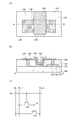
本実施の形態では、本発明の一態様を適用した半導体記憶装置である不揮発性メモリを構成するトランジスタおよびキャパシタの構造、回路構成、ならびにその作製方法について図1乃至図3を用いて説明する。
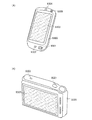
本実施の形態では、実施の形態1を適用した電子機器の例について説明する。
104 導電膜
105 導電膜
106 酸化物半導体膜
108 絶縁膜
120 絶縁膜
124 導電膜
125 導電膜
126 半導体膜
128 絶縁膜
144 導電膜
150 トランジスタ
160 キャパシタ
170 トランジスタ
9300 筐体
9301 ボタン
9302 マイクロフォン
9303 表示部
9304 スピーカ
9305 カメラ
9320 筐体
9321 ボタン
9322 マイクロフォン
9323 表示部
Claims (5)
- 半導体と、
前記半導体上方の第1の絶縁膜と、
前記第1の絶縁膜上方の第1の導電膜と、
前記第1の絶縁膜上方の第2の導電膜と、
前記第1の絶縁膜上方に設けられ、前記第1の導電膜と前記第2の導電膜との間に、前記第1の絶縁膜に達する溝部を有する第2の絶縁膜と、
前記第1の導電膜および前記第2の導電膜と接する領域を有し、前記溝部の側面および底面と接する領域を有する酸化物半導体膜と、
前記酸化物半導体膜上方の第3の絶縁膜と、
前記第3の絶縁膜上方の第3の導電膜と、
を有し、
前記第1の導電膜は、前記第1の絶縁膜を介して前記半導体と重なる領域を有し、
前記第3の導電膜は、前記第3の絶縁膜を介して前記酸化物半導体膜と重なる領域を有し、
前記酸化物半導体膜は、前記第1の絶縁膜と接する領域を有することを特徴とする半導体記憶装置。 - 半導体と、
前記半導体上方の第1の絶縁膜と、
前記第1の絶縁膜上方の第1の導電膜と、
前記第1の絶縁膜上方の第2の導電膜と、
前記第1の絶縁膜上方に設けられ、前記第1の導電膜と前記第2の導電膜との間に、前記第1の絶縁膜に達する溝部を有する第2の絶縁膜と、
前記第1の導電膜および前記第2の導電膜と接する領域を有し、前記溝部の側面および底面と接する領域を有する酸化物半導体膜と、
前記酸化物半導体膜上方の第3の絶縁膜と、
前記第3の絶縁膜上方の第3の導電膜と、
前記第3の絶縁膜上方の第4の導電膜と、
を有し、
前記第1の導電膜は、前記第1の絶縁膜を介して前記半導体と重なる領域を有し、
前記第3の導電膜は、前記第3の絶縁膜を介して前記酸化物半導体膜と重なる領域を有し、
前記第4の導電膜は、前記第3の絶縁膜および前記酸化物半導体膜を介して前記第1の導電膜と重なる領域を有し、
前記酸化物半導体膜は、前記第1の絶縁膜と接する領域を有することを特徴とする半導体記憶装置。 - 請求項2において、
前記第4の導電膜は、前記第3の導電膜と同一材料を有することを特徴とする半導体記憶装置。 - 請求項1乃至3のいずれか一項において、
前記第2の導電膜は、前記第1の導電膜と同一材料を有することを特徴とする半導体記憶装置。 - 請求項1乃至4のいずれか一項において、
前記第2の絶縁膜は、前記第1の導電膜および前記第2の導電膜の上面を露出するように設けられることを特徴とする半導体記憶装置。
Priority Applications (1)
| Application Number | Priority Date | Filing Date | Title |
|---|---|---|---|
| JP2012048891A JP5961409B2 (ja) | 2011-03-10 | 2012-03-06 | 半導体記憶装置 |
Applications Claiming Priority (3)
| Application Number | Priority Date | Filing Date | Title |
|---|---|---|---|
| JP2011052270 | 2011-03-10 | ||
| JP2011052270 | 2011-03-10 | ||
| JP2012048891A JP5961409B2 (ja) | 2011-03-10 | 2012-03-06 | 半導体記憶装置 |
Related Child Applications (1)
| Application Number | Title | Priority Date | Filing Date |
|---|---|---|---|
| JP2016126477A Division JP6197075B2 (ja) | 2011-03-10 | 2016-06-27 | 半導体装置 |
Publications (3)
| Publication Number | Publication Date |
|---|---|
| JP2012199536A JP2012199536A (ja) | 2012-10-18 |
| JP2012199536A5 JP2012199536A5 (ja) | 2015-03-26 |
| JP5961409B2 true JP5961409B2 (ja) | 2016-08-02 |
Family
ID=46794749
Family Applications (2)
| Application Number | Title | Priority Date | Filing Date |
|---|---|---|---|
| JP2012048891A Expired - Fee Related JP5961409B2 (ja) | 2011-03-10 | 2012-03-06 | 半導体記憶装置 |
| JP2016126477A Expired - Fee Related JP6197075B2 (ja) | 2011-03-10 | 2016-06-27 | 半導体装置 |
Family Applications After (1)
| Application Number | Title | Priority Date | Filing Date |
|---|---|---|---|
| JP2016126477A Expired - Fee Related JP6197075B2 (ja) | 2011-03-10 | 2016-06-27 | 半導体装置 |
Country Status (4)
| Country | Link |
|---|---|
| US (1) | US8772849B2 (ja) |
| JP (2) | JP5961409B2 (ja) |
| KR (2) | KR101954592B1 (ja) |
| TW (1) | TWI550829B (ja) |
Families Citing this family (18)
| Publication number | Priority date | Publication date | Assignee | Title |
|---|---|---|---|---|
| KR100753600B1 (ko) * | 2007-05-28 | 2007-08-30 | 원철수 | 몰딩부재 장착유닛 및 이를 이용한 몰딩부재 코팅장치 |
| US20120298998A1 (en) * | 2011-05-25 | 2012-11-29 | Semiconductor Energy Laboratory Co., Ltd. | Method for forming oxide semiconductor film, semiconductor device, and method for manufacturing semiconductor device |
| WO2013054823A1 (en) * | 2011-10-14 | 2013-04-18 | Semiconductor Energy Laboratory Co., Ltd. | Semiconductor device and manufacturing method thereof |
| US9607991B2 (en) | 2013-09-05 | 2017-03-28 | Semiconductor Energy Laboratory Co., Ltd. | Semiconductor device |
| WO2015145292A1 (en) | 2014-03-28 | 2015-10-01 | Semiconductor Energy Laboratory Co., Ltd. | Transistor and semiconductor device |
| TWI735206B (zh) | 2014-04-10 | 2021-08-01 | 日商半導體能源研究所股份有限公司 | 記憶體裝置及半導體裝置 |
| WO2015170220A1 (en) | 2014-05-09 | 2015-11-12 | Semiconductor Energy Laboratory Co., Ltd. | Memory device and electronic device |
| US10671204B2 (en) | 2015-05-04 | 2020-06-02 | Semiconductor Energy Laboratory Co., Ltd. | Touch panel and data processor |
| US9741400B2 (en) | 2015-11-05 | 2017-08-22 | Semiconductor Energy Laboratory Co., Ltd. | Semiconductor device, memory device, electronic device, and method for operating the semiconductor device |
| DE102021101243A1 (de) | 2020-05-29 | 2021-12-02 | Taiwan Semiconductor Manufacturing Co., Ltd. | Speicherblock-kanalregionen |
| US11695073B2 (en) | 2020-05-29 | 2023-07-04 | Taiwan Semiconductor Manufacturing Co., Ltd. | Memory array gate structures |
| DE102020127831A1 (de) | 2020-05-29 | 2021-12-02 | Taiwan Semiconductor Manufacturing Co., Ltd. | Speicherarray-gatestrukturen |
| US11710790B2 (en) | 2020-05-29 | 2023-07-25 | Taiwan Semiconductor Manufacturing Company, Ltd. | Memory array channel regions |
| US11729987B2 (en) | 2020-06-30 | 2023-08-15 | Taiwan Semiconductor Manufacturing Company, Ltd. | Memory array source/drain electrode structures |
| US11640974B2 (en) | 2020-06-30 | 2023-05-02 | Taiwan Semiconductor Manufacturing Co., Ltd. | Memory array isolation structures |
| US11647634B2 (en) | 2020-07-16 | 2023-05-09 | Taiwan Semiconductor Manufacturing Co., Ltd. | Three-dimensional memory device and method |
| US11355516B2 (en) | 2020-07-16 | 2022-06-07 | Taiwan Semiconductor Manufacturing Co., Ltd. | Three-dimensional memory device and method |
| WO2024141883A1 (ja) * | 2022-12-28 | 2024-07-04 | 株式会社半導体エネルギー研究所 | 半導体装置 |
Family Cites Families (121)
| Publication number | Priority date | Publication date | Assignee | Title |
|---|---|---|---|---|
| JPS6034199B2 (ja) | 1980-12-20 | 1985-08-07 | 株式会社東芝 | 半導体記憶装置 |
| US5317432A (en) | 1991-09-04 | 1994-05-31 | Sony Corporation | Liquid crystal display device with a capacitor and a thin film transistor in a trench for each pixel |
| JP3287038B2 (ja) * | 1991-12-19 | 2002-05-27 | ソニー株式会社 | 液晶表示装置 |
| KR950007358B1 (ko) * | 1992-07-01 | 1995-07-10 | 현대전자산업주식회사 | 박막트랜지스터의 제조방법 |
| JP3209600B2 (ja) * | 1992-12-24 | 2001-09-17 | キヤノン株式会社 | 薄膜トランジスタの製造方法 |
| JP2921812B2 (ja) | 1992-12-24 | 1999-07-19 | シャープ株式会社 | 不揮発性半導体記憶装置 |
| JP3298974B2 (ja) | 1993-03-23 | 2002-07-08 | 電子科学株式会社 | 昇温脱離ガス分析装置 |
| DE69635107D1 (de) | 1995-08-03 | 2005-09-29 | Koninkl Philips Electronics Nv | Halbleiteranordnung mit einem transparenten schaltungselement |
| JP3625598B2 (ja) | 1995-12-30 | 2005-03-02 | 三星電子株式会社 | 液晶表示装置の製造方法 |
| JP4170454B2 (ja) | 1998-07-24 | 2008-10-22 | Hoya株式会社 | 透明導電性酸化物薄膜を有する物品及びその製造方法 |
| JP2000150861A (ja) | 1998-11-16 | 2000-05-30 | Tdk Corp | 酸化物薄膜 |
| JP3276930B2 (ja) | 1998-11-17 | 2002-04-22 | 科学技術振興事業団 | トランジスタ及び半導体装置 |
| TW460731B (en) | 1999-09-03 | 2001-10-21 | Ind Tech Res Inst | Electrode structure and production method of wide viewing angle LCD |
| JP3915868B2 (ja) | 2000-07-07 | 2007-05-16 | セイコーエプソン株式会社 | 強誘電体メモリ装置およびその製造方法 |
| JP4089858B2 (ja) | 2000-09-01 | 2008-05-28 | 国立大学法人東北大学 | 半導体デバイス |
| JP3749101B2 (ja) * | 2000-09-14 | 2006-02-22 | 株式会社ルネサステクノロジ | 半導体装置 |
| KR20020038482A (ko) | 2000-11-15 | 2002-05-23 | 모리시타 요이찌 | 박막 트랜지스터 어레이, 그 제조방법 및 그것을 이용한표시패널 |
| JP3997731B2 (ja) | 2001-03-19 | 2007-10-24 | 富士ゼロックス株式会社 | 基材上に結晶性半導体薄膜を形成する方法 |
| JP2002289859A (ja) | 2001-03-23 | 2002-10-04 | Minolta Co Ltd | 薄膜トランジスタ |
| JP2002368226A (ja) | 2001-06-11 | 2002-12-20 | Sharp Corp | 半導体装置、半導体記憶装置及びその製造方法、並びに携帯情報機器 |
| JP3925839B2 (ja) | 2001-09-10 | 2007-06-06 | シャープ株式会社 | 半導体記憶装置およびその試験方法 |
| JP4090716B2 (ja) | 2001-09-10 | 2008-05-28 | 雅司 川崎 | 薄膜トランジスタおよびマトリクス表示装置 |
| JP4164562B2 (ja) | 2002-09-11 | 2008-10-15 | 独立行政法人科学技術振興機構 | ホモロガス薄膜を活性層として用いる透明薄膜電界効果型トランジスタ |
| WO2003040441A1 (fr) | 2001-11-05 | 2003-05-15 | Japan Science And Technology Agency | Film mince monocristallin homologue a super-reseau naturel, procede de preparation et dispositif dans lequel est utilise ledit film mince monocristallin |
| JP4083486B2 (ja) | 2002-02-21 | 2008-04-30 | 独立行政法人科学技術振興機構 | LnCuO(S,Se,Te)単結晶薄膜の製造方法 |
| US7049190B2 (en) | 2002-03-15 | 2006-05-23 | Sanyo Electric Co., Ltd. | Method for forming ZnO film, method for forming ZnO semiconductor layer, method for fabricating semiconductor device, and semiconductor device |
| JP3933591B2 (ja) | 2002-03-26 | 2007-06-20 | 淳二 城戸 | 有機エレクトロルミネッセント素子 |
| US7339187B2 (en) | 2002-05-21 | 2008-03-04 | State Of Oregon Acting By And Through The Oregon State Board Of Higher Education On Behalf Of Oregon State University | Transistor structures |
| JP2004022625A (ja) | 2002-06-13 | 2004-01-22 | Murata Mfg Co Ltd | 半導体デバイス及び該半導体デバイスの製造方法 |
| US7105868B2 (en) | 2002-06-24 | 2006-09-12 | Cermet, Inc. | High-electron mobility transistor with zinc oxide |
| US7067843B2 (en) | 2002-10-11 | 2006-06-27 | E. I. Du Pont De Nemours And Company | Transparent oxide semiconductor thin film transistors |
| JP4166105B2 (ja) | 2003-03-06 | 2008-10-15 | シャープ株式会社 | 半導体装置およびその製造方法 |
| JP2004273732A (ja) | 2003-03-07 | 2004-09-30 | Sharp Corp | アクティブマトリクス基板およびその製造方法 |
| JP4108633B2 (ja) | 2003-06-20 | 2008-06-25 | シャープ株式会社 | 薄膜トランジスタおよびその製造方法ならびに電子デバイス |
| US7262463B2 (en) | 2003-07-25 | 2007-08-28 | Hewlett-Packard Development Company, L.P. | Transistor including a deposited channel region having a doped portion |
| US7145174B2 (en) | 2004-03-12 | 2006-12-05 | Hewlett-Packard Development Company, Lp. | Semiconductor device |
| US7282782B2 (en) | 2004-03-12 | 2007-10-16 | Hewlett-Packard Development Company, L.P. | Combined binary oxide semiconductor device |
| US7297977B2 (en) | 2004-03-12 | 2007-11-20 | Hewlett-Packard Development Company, L.P. | Semiconductor device |
| EP1737044B1 (en) | 2004-03-12 | 2014-12-10 | Japan Science and Technology Agency | Amorphous oxide and thin film transistor |
| US7211825B2 (en) | 2004-06-14 | 2007-05-01 | Yi-Chi Shih | Indium oxide-based thin film transistors and circuits |
| JP2006049413A (ja) | 2004-08-02 | 2006-02-16 | Fujitsu Ltd | 半導体装置及びその製造方法 |
| JP2006100760A (ja) | 2004-09-02 | 2006-04-13 | Casio Comput Co Ltd | 薄膜トランジスタおよびその製造方法 |
| US7285501B2 (en) | 2004-09-17 | 2007-10-23 | Hewlett-Packard Development Company, L.P. | Method of forming a solution processed device |
| JP4143589B2 (ja) | 2004-10-15 | 2008-09-03 | エルピーダメモリ株式会社 | 半導体装置の製造方法 |
| US7298084B2 (en) | 2004-11-02 | 2007-11-20 | 3M Innovative Properties Company | Methods and displays utilizing integrated zinc oxide row and column drivers in conjunction with organic light emitting diodes |
| US7863611B2 (en) | 2004-11-10 | 2011-01-04 | Canon Kabushiki Kaisha | Integrated circuits utilizing amorphous oxides |
| US7791072B2 (en) | 2004-11-10 | 2010-09-07 | Canon Kabushiki Kaisha | Display |
| WO2006051995A1 (en) | 2004-11-10 | 2006-05-18 | Canon Kabushiki Kaisha | Field effect transistor employing an amorphous oxide |
| RU2358354C2 (ru) | 2004-11-10 | 2009-06-10 | Кэнон Кабусики Кайся | Светоизлучающее устройство |
| US7453065B2 (en) | 2004-11-10 | 2008-11-18 | Canon Kabushiki Kaisha | Sensor and image pickup device |
| US7829444B2 (en) | 2004-11-10 | 2010-11-09 | Canon Kabushiki Kaisha | Field effect transistor manufacturing method |
| CN102945857B (zh) | 2004-11-10 | 2015-06-03 | 佳能株式会社 | 无定形氧化物和场效应晶体管 |
| US7579224B2 (en) | 2005-01-21 | 2009-08-25 | Semiconductor Energy Laboratory Co., Ltd. | Method for manufacturing a thin film semiconductor device |
| TWI569441B (zh) | 2005-01-28 | 2017-02-01 | 半導體能源研究所股份有限公司 | 半導體裝置,電子裝置,和半導體裝置的製造方法 |
| TWI505473B (zh) | 2005-01-28 | 2015-10-21 | 半導體能源研究所股份有限公司 | 半導體裝置,電子裝置,和半導體裝置的製造方法 |
| US7858451B2 (en) | 2005-02-03 | 2010-12-28 | Semiconductor Energy Laboratory Co., Ltd. | Electronic device, semiconductor device and manufacturing method thereof |
| US7948171B2 (en) | 2005-02-18 | 2011-05-24 | Semiconductor Energy Laboratory Co., Ltd. | Light emitting device |
| US20060197092A1 (en) | 2005-03-03 | 2006-09-07 | Randy Hoffman | System and method for forming conductive material on a substrate |
| US8681077B2 (en) | 2005-03-18 | 2014-03-25 | Semiconductor Energy Laboratory Co., Ltd. | Semiconductor device, and display device, driving method and electronic apparatus thereof |
| US7544967B2 (en) | 2005-03-28 | 2009-06-09 | Massachusetts Institute Of Technology | Low voltage flexible organic/transparent transistor for selective gas sensing, photodetecting and CMOS device applications |
| US7645478B2 (en) | 2005-03-31 | 2010-01-12 | 3M Innovative Properties Company | Methods of making displays |
| US8300031B2 (en) | 2005-04-20 | 2012-10-30 | Semiconductor Energy Laboratory Co., Ltd. | Semiconductor device comprising transistor having gate and drain connected through a current-voltage conversion element |
| JP2006344849A (ja) | 2005-06-10 | 2006-12-21 | Casio Comput Co Ltd | 薄膜トランジスタ |
| US7402506B2 (en) | 2005-06-16 | 2008-07-22 | Eastman Kodak Company | Methods of making thin film transistors comprising zinc-oxide-based semiconductor materials and transistors made thereby |
| US7691666B2 (en) | 2005-06-16 | 2010-04-06 | Eastman Kodak Company | Methods of making thin film transistors comprising zinc-oxide-based semiconductor materials and transistors made thereby |
| US7507618B2 (en) | 2005-06-27 | 2009-03-24 | 3M Innovative Properties Company | Method for making electronic devices using metal oxide nanoparticles |
| KR100711890B1 (ko) | 2005-07-28 | 2007-04-25 | 삼성에스디아이 주식회사 | 유기 발광표시장치 및 그의 제조방법 |
| JP2007059128A (ja) | 2005-08-23 | 2007-03-08 | Canon Inc | 有機el表示装置およびその製造方法 |
| JP4280736B2 (ja) | 2005-09-06 | 2009-06-17 | キヤノン株式会社 | 半導体素子 |
| JP2007073705A (ja) | 2005-09-06 | 2007-03-22 | Canon Inc | 酸化物半導体チャネル薄膜トランジスタおよびその製造方法 |
| JP5116225B2 (ja) | 2005-09-06 | 2013-01-09 | キヤノン株式会社 | 酸化物半導体デバイスの製造方法 |
| JP4850457B2 (ja) | 2005-09-06 | 2012-01-11 | キヤノン株式会社 | 薄膜トランジスタ及び薄膜ダイオード |
| EP1995787A3 (en) | 2005-09-29 | 2012-01-18 | Semiconductor Energy Laboratory Co, Ltd. | Semiconductor device having oxide semiconductor layer and manufacturing method therof |
| JP5037808B2 (ja) | 2005-10-20 | 2012-10-03 | キヤノン株式会社 | アモルファス酸化物を用いた電界効果型トランジスタ、及び該トランジスタを用いた表示装置 |
| KR101050767B1 (ko) | 2005-11-15 | 2011-07-20 | 가부시키가이샤 한도오따이 에네루기 켄큐쇼 | 반도체장치 제조방법 |
| TWI292281B (en) | 2005-12-29 | 2008-01-01 | Ind Tech Res Inst | Pixel structure of active organic light emitting diode and method of fabricating the same |
| US7867636B2 (en) | 2006-01-11 | 2011-01-11 | Murata Manufacturing Co., Ltd. | Transparent conductive film and method for manufacturing the same |
| JP4977478B2 (ja) | 2006-01-21 | 2012-07-18 | 三星電子株式会社 | ZnOフィルム及びこれを用いたTFTの製造方法 |
| US7576394B2 (en) | 2006-02-02 | 2009-08-18 | Kochi Industrial Promotion Center | Thin film transistor including low resistance conductive thin films and manufacturing method thereof |
| US7977169B2 (en) | 2006-02-15 | 2011-07-12 | Kochi Industrial Promotion Center | Semiconductor device including active layer made of zinc oxide with controlled orientations and manufacturing method thereof |
| JP4935138B2 (ja) * | 2006-03-23 | 2012-05-23 | セイコーエプソン株式会社 | 回路基板、回路基板の製造方法、電気光学装置および電子機器 |
| KR20070101595A (ko) | 2006-04-11 | 2007-10-17 | 삼성전자주식회사 | ZnO TFT |
| US20070252928A1 (en) | 2006-04-28 | 2007-11-01 | Toppan Printing Co., Ltd. | Structure, transmission type liquid crystal display, reflection type display and manufacturing method thereof |
| JP5028033B2 (ja) | 2006-06-13 | 2012-09-19 | キヤノン株式会社 | 酸化物半導体膜のドライエッチング方法 |
| JP2008004738A (ja) | 2006-06-22 | 2008-01-10 | Elpida Memory Inc | 半導体装置及びその製造方法 |
| JP4609797B2 (ja) | 2006-08-09 | 2011-01-12 | Nec液晶テクノロジー株式会社 | 薄膜デバイス及びその製造方法 |
| JP4999400B2 (ja) | 2006-08-09 | 2012-08-15 | キヤノン株式会社 | 酸化物半導体膜のドライエッチング方法 |
| JP4332545B2 (ja) | 2006-09-15 | 2009-09-16 | キヤノン株式会社 | 電界効果型トランジスタ及びその製造方法 |
| JP4274219B2 (ja) | 2006-09-27 | 2009-06-03 | セイコーエプソン株式会社 | 電子デバイス、有機エレクトロルミネッセンス装置、有機薄膜半導体装置 |
| JP5164357B2 (ja) | 2006-09-27 | 2013-03-21 | キヤノン株式会社 | 半導体装置及び半導体装置の製造方法 |
| US7622371B2 (en) | 2006-10-10 | 2009-11-24 | Hewlett-Packard Development Company, L.P. | Fused nanocrystal thin film semiconductor and method |
| US7772021B2 (en) | 2006-11-29 | 2010-08-10 | Samsung Electronics Co., Ltd. | Flat panel displays comprising a thin-film transistor having a semiconductive oxide in its channel and methods of fabricating the same for use in flat panel displays |
| JP2008140684A (ja) | 2006-12-04 | 2008-06-19 | Toppan Printing Co Ltd | カラーelディスプレイおよびその製造方法 |
| KR101303578B1 (ko) | 2007-01-05 | 2013-09-09 | 삼성전자주식회사 | 박막 식각 방법 |
| US8207063B2 (en) | 2007-01-26 | 2012-06-26 | Eastman Kodak Company | Process for atomic layer deposition |
| KR100851215B1 (ko) | 2007-03-14 | 2008-08-07 | 삼성에스디아이 주식회사 | 박막 트랜지스터 및 이를 이용한 유기 전계 발광표시장치 |
| US7795613B2 (en) | 2007-04-17 | 2010-09-14 | Toppan Printing Co., Ltd. | Structure with transistor |
| KR101325053B1 (ko) | 2007-04-18 | 2013-11-05 | 삼성디스플레이 주식회사 | 박막 트랜지스터 기판 및 이의 제조 방법 |
| KR20080094300A (ko) | 2007-04-19 | 2008-10-23 | 삼성전자주식회사 | 박막 트랜지스터 및 그 제조 방법과 박막 트랜지스터를포함하는 평판 디스플레이 |
| KR101334181B1 (ko) | 2007-04-20 | 2013-11-28 | 삼성전자주식회사 | 선택적으로 결정화된 채널층을 갖는 박막 트랜지스터 및 그제조 방법 |
| US8274078B2 (en) | 2007-04-25 | 2012-09-25 | Canon Kabushiki Kaisha | Metal oxynitride semiconductor containing zinc |
| KR101345376B1 (ko) | 2007-05-29 | 2013-12-24 | 삼성전자주식회사 | ZnO 계 박막 트랜지스터 및 그 제조방법 |
| JP2009016368A (ja) * | 2007-06-29 | 2009-01-22 | Ricoh Co Ltd | メモリーデバイス |
| JP5430846B2 (ja) | 2007-12-03 | 2014-03-05 | 株式会社半導体エネルギー研究所 | 半導体装置の作製方法 |
| JP5215158B2 (ja) | 2007-12-17 | 2013-06-19 | 富士フイルム株式会社 | 無機結晶性配向膜及びその製造方法、半導体デバイス |
| JP5305696B2 (ja) | 2008-03-06 | 2013-10-02 | キヤノン株式会社 | 半導体素子の処理方法 |
| JP2009253249A (ja) | 2008-04-11 | 2009-10-29 | Elpida Memory Inc | 半導体装置、その製造方法、及び、データ処理システム |
| US7893494B2 (en) | 2008-06-18 | 2011-02-22 | International Business Machines Corporation | Method and structure for SOI body contact FET with reduced parasitic capacitance |
| JP4623179B2 (ja) | 2008-09-18 | 2011-02-02 | ソニー株式会社 | 薄膜トランジスタおよびその製造方法 |
| JP5451280B2 (ja) | 2008-10-09 | 2014-03-26 | キヤノン株式会社 | ウルツ鉱型結晶成長用基板およびその製造方法ならびに半導体装置 |
| CN103456794B (zh) | 2008-12-19 | 2016-08-10 | 株式会社半导体能源研究所 | 晶体管的制造方法 |
| US8461582B2 (en) * | 2009-03-05 | 2013-06-11 | Semiconductor Energy Laboratory Co., Ltd. | Semiconductor device and method for manufacturing the same |
| WO2011007677A1 (en) * | 2009-07-17 | 2011-01-20 | Semiconductor Energy Laboratory Co., Ltd. | Semiconductor device and method for manufacturing the same |
| WO2012002186A1 (en) * | 2010-07-02 | 2012-01-05 | Semiconductor Energy Laboratory Co., Ltd. | Semiconductor device |
| WO2012029637A1 (en) * | 2010-09-03 | 2012-03-08 | Semiconductor Energy Laboratory Co., Ltd. | Semiconductor device and driving method thereof |
| WO2012102183A1 (en) | 2011-01-26 | 2012-08-02 | Semiconductor Energy Laboratory Co., Ltd. | Semiconductor device and manufacturing method thereof |
| TWI552345B (zh) | 2011-01-26 | 2016-10-01 | 半導體能源研究所股份有限公司 | 半導體裝置及其製造方法 |
| WO2012102182A1 (en) | 2011-01-26 | 2012-08-02 | Semiconductor Energy Laboratory Co., Ltd. | Semiconductor device |
| US9691772B2 (en) | 2011-03-03 | 2017-06-27 | Semiconductor Energy Laboratory Co., Ltd. | Semiconductor memory device including memory cell which includes transistor and capacitor |
| US8841664B2 (en) * | 2011-03-04 | 2014-09-23 | Semiconductor Energy Laboratory Co., Ltd. | Semiconductor device |
| US8809854B2 (en) * | 2011-04-22 | 2014-08-19 | Semiconductor Energy Laboratory Co., Ltd. | Semiconductor device |
-
2012
- 2012-03-02 US US13/410,608 patent/US8772849B2/en not_active Expired - Fee Related
- 2012-03-06 TW TW101107467A patent/TWI550829B/zh not_active IP Right Cessation
- 2012-03-06 KR KR1020120022669A patent/KR101954592B1/ko not_active Expired - Fee Related
- 2012-03-06 JP JP2012048891A patent/JP5961409B2/ja not_active Expired - Fee Related
-
2016
- 2016-06-27 JP JP2016126477A patent/JP6197075B2/ja not_active Expired - Fee Related
-
2019
- 2019-02-22 KR KR1020190020958A patent/KR101988211B1/ko not_active Expired - Fee Related
Also Published As
| Publication number | Publication date |
|---|---|
| JP6197075B2 (ja) | 2017-09-13 |
| JP2016213479A (ja) | 2016-12-15 |
| KR20190022591A (ko) | 2019-03-06 |
| KR101988211B1 (ko) | 2019-06-13 |
| US20120228687A1 (en) | 2012-09-13 |
| JP2012199536A (ja) | 2012-10-18 |
| US8772849B2 (en) | 2014-07-08 |
| TWI550829B (zh) | 2016-09-21 |
| KR20120103466A (ko) | 2012-09-19 |
| KR101954592B1 (ko) | 2019-03-06 |
| TW201244065A (en) | 2012-11-01 |
Similar Documents
| Publication | Publication Date | Title |
|---|---|---|
| JP5961409B2 (ja) | 半導体記憶装置 | |
| JP7360485B2 (ja) | 撮像装置 | |
| JP5912655B2 (ja) | 半導体装置 | |
| JP7458467B2 (ja) | 撮像装置 | |
| JP6053098B2 (ja) | 半導体装置 | |
| TWI536569B (zh) | 半導體裝置 | |
| TWI527127B (zh) | 半導體裝置及其製造方法 | |
| US9379223B2 (en) | Oxide semiconductor film, semiconductor device, and manufacturing method of semiconductor device | |
| JP2020025334A (ja) | 撮像装置 | |
| JP6633723B2 (ja) | 半導体装置の作製方法 | |
| JP5955616B2 (ja) | 半導体記憶装置 | |
| JP2012256877A (ja) | 半導体記憶装置およびその作製方法 | |
| JP2012216795A (ja) | 半導体装置および該半導体装置の作製方法 | |
| JP2012191185A (ja) | 半導体装置および半導体装置の作製方法 |
Legal Events
| Date | Code | Title | Description |
|---|---|---|---|
| A521 | Request for written amendment filed |
Free format text: JAPANESE INTERMEDIATE CODE: A523 Effective date: 20150204 |
|
| A621 | Written request for application examination |
Free format text: JAPANESE INTERMEDIATE CODE: A621 Effective date: 20150204 |
|
| A977 | Report on retrieval |
Free format text: JAPANESE INTERMEDIATE CODE: A971007 Effective date: 20151124 |
|
| A131 | Notification of reasons for refusal |
Free format text: JAPANESE INTERMEDIATE CODE: A131 Effective date: 20151201 |
|
| A521 | Request for written amendment filed |
Free format text: JAPANESE INTERMEDIATE CODE: A523 Effective date: 20160111 |
|
| TRDD | Decision of grant or rejection written | ||
| A01 | Written decision to grant a patent or to grant a registration (utility model) |
Free format text: JAPANESE INTERMEDIATE CODE: A01 Effective date: 20160614 |
|
| A61 | First payment of annual fees (during grant procedure) |
Free format text: JAPANESE INTERMEDIATE CODE: A61 Effective date: 20160627 |
|
| R150 | Certificate of patent or registration of utility model |
Ref document number: 5961409 Country of ref document: JP Free format text: JAPANESE INTERMEDIATE CODE: R150 |
|
| R250 | Receipt of annual fees |
Free format text: JAPANESE INTERMEDIATE CODE: R250 |
|
| R250 | Receipt of annual fees |
Free format text: JAPANESE INTERMEDIATE CODE: R250 |
|
| LAPS | Cancellation because of no payment of annual fees |