JP5961409B2 - Semiconductor memory device - Google Patents
Semiconductor memory device Download PDFInfo
- Publication number
- JP5961409B2 JP5961409B2 JP2012048891A JP2012048891A JP5961409B2 JP 5961409 B2 JP5961409 B2 JP 5961409B2 JP 2012048891 A JP2012048891 A JP 2012048891A JP 2012048891 A JP2012048891 A JP 2012048891A JP 5961409 B2 JP5961409 B2 JP 5961409B2
- Authority
- JP
- Japan
- Prior art keywords
- film
- insulating film
- conductive film
- transistor
- oxide semiconductor
- Prior art date
- Legal status (The legal status is an assumption and is not a legal conclusion. Google has not performed a legal analysis and makes no representation as to the accuracy of the status listed.)
- Expired - Fee Related
Links
- 239000004065 semiconductor Substances 0.000 title claims description 138
- 239000000463 material Substances 0.000 claims description 35
- 239000000758 substrate Substances 0.000 description 30
- 239000003990 capacitor Substances 0.000 description 28
- QVGXLLKOCUKJST-UHFFFAOYSA-N atomic oxygen Chemical compound [O] QVGXLLKOCUKJST-UHFFFAOYSA-N 0.000 description 25
- 230000015654 memory Effects 0.000 description 25
- 239000001301 oxygen Substances 0.000 description 25
- 229910052760 oxygen Inorganic materials 0.000 description 25
- 238000000034 method Methods 0.000 description 21
- 239000013078 crystal Substances 0.000 description 16
- 230000006870 function Effects 0.000 description 16
- 229910007541 Zn O Inorganic materials 0.000 description 12
- 238000004458 analytical method Methods 0.000 description 12
- 239000012535 impurity Substances 0.000 description 12
- 125000004430 oxygen atom Chemical group O* 0.000 description 12
- 239000010410 layer Substances 0.000 description 11
- 238000010438 heat treatment Methods 0.000 description 10
- 125000004429 atom Chemical group 0.000 description 8
- 230000015572 biosynthetic process Effects 0.000 description 8
- 230000010354 integration Effects 0.000 description 8
- 239000011701 zinc Substances 0.000 description 8
- XUIMIQQOPSSXEZ-UHFFFAOYSA-N Silicon Chemical compound [Si] XUIMIQQOPSSXEZ-UHFFFAOYSA-N 0.000 description 7
- 239000000969 carrier Substances 0.000 description 7
- 229910052733 gallium Inorganic materials 0.000 description 7
- 239000001257 hydrogen Substances 0.000 description 7
- 229910052739 hydrogen Inorganic materials 0.000 description 7
- 150000002500 ions Chemical class 0.000 description 7
- IJGRMHOSHXDMSA-UHFFFAOYSA-N Atomic nitrogen Chemical compound N#N IJGRMHOSHXDMSA-UHFFFAOYSA-N 0.000 description 6
- VYPSYNLAJGMNEJ-UHFFFAOYSA-N silicon dioxide Inorganic materials O=[Si]=O VYPSYNLAJGMNEJ-UHFFFAOYSA-N 0.000 description 6
- UFHFLCQGNIYNRP-UHFFFAOYSA-N Hydrogen Chemical compound [H][H] UFHFLCQGNIYNRP-UHFFFAOYSA-N 0.000 description 5
- 238000004519 manufacturing process Methods 0.000 description 5
- 229910052751 metal Inorganic materials 0.000 description 5
- 238000000206 photolithography Methods 0.000 description 5
- 229910052710 silicon Inorganic materials 0.000 description 5
- 239000010703 silicon Substances 0.000 description 5
- 229910052814 silicon oxide Inorganic materials 0.000 description 5
- 239000011734 sodium Substances 0.000 description 5
- 230000006866 deterioration Effects 0.000 description 4
- 230000000694 effects Effects 0.000 description 4
- 229910052738 indium Inorganic materials 0.000 description 4
- 239000002184 metal Substances 0.000 description 4
- 229910019092 Mg-O Inorganic materials 0.000 description 3
- 229910019395 Mg—O Inorganic materials 0.000 description 3
- 229910052581 Si3N4 Inorganic materials 0.000 description 3
- 229910052783 alkali metal Inorganic materials 0.000 description 3
- 150000001340 alkali metals Chemical class 0.000 description 3
- 229910052782 aluminium Inorganic materials 0.000 description 3
- 230000007547 defect Effects 0.000 description 3
- 238000010586 diagram Methods 0.000 description 3
- 239000007789 gas Substances 0.000 description 3
- 230000014759 maintenance of location Effects 0.000 description 3
- 229910044991 metal oxide Inorganic materials 0.000 description 3
- 150000004706 metal oxides Chemical group 0.000 description 3
- 229910052757 nitrogen Inorganic materials 0.000 description 3
- HQVNEWCFYHHQES-UHFFFAOYSA-N silicon nitride Chemical compound N12[Si]34N5[Si]62N3[Si]51N64 HQVNEWCFYHHQES-UHFFFAOYSA-N 0.000 description 3
- 238000004544 sputter deposition Methods 0.000 description 3
- 229910052725 zinc Inorganic materials 0.000 description 3
- XKRFYHLGVUSROY-UHFFFAOYSA-N Argon Chemical compound [Ar] XKRFYHLGVUSROY-UHFFFAOYSA-N 0.000 description 2
- OAICVXFJPJFONN-UHFFFAOYSA-N Phosphorus Chemical compound [P] OAICVXFJPJFONN-UHFFFAOYSA-N 0.000 description 2
- 229910000577 Silicon-germanium Inorganic materials 0.000 description 2
- 238000004833 X-ray photoelectron spectroscopy Methods 0.000 description 2
- LEVVHYCKPQWKOP-UHFFFAOYSA-N [Si].[Ge] Chemical compound [Si].[Ge] LEVVHYCKPQWKOP-UHFFFAOYSA-N 0.000 description 2
- 229910052784 alkaline earth metal Inorganic materials 0.000 description 2
- 150000001342 alkaline earth metals Chemical class 0.000 description 2
- 238000006243 chemical reaction Methods 0.000 description 2
- 150000001875 compounds Chemical class 0.000 description 2
- 238000000151 deposition Methods 0.000 description 2
- 238000003795 desorption Methods 0.000 description 2
- 238000005530 etching Methods 0.000 description 2
- 230000005284 excitation Effects 0.000 description 2
- 230000005669 field effect Effects 0.000 description 2
- 150000002431 hydrogen Chemical class 0.000 description 2
- 229910052748 manganese Inorganic materials 0.000 description 2
- 239000012528 membrane Substances 0.000 description 2
- 238000001451 molecular beam epitaxy Methods 0.000 description 2
- 230000003647 oxidation Effects 0.000 description 2
- 238000007254 oxidation reaction Methods 0.000 description 2
- 229910052698 phosphorus Inorganic materials 0.000 description 2
- 239000011574 phosphorus Substances 0.000 description 2
- 238000005268 plasma chemical vapour deposition Methods 0.000 description 2
- 238000004335 scaling law Methods 0.000 description 2
- 238000001004 secondary ion mass spectrometry Methods 0.000 description 2
- LIVNPJMFVYWSIS-UHFFFAOYSA-N silicon monoxide Chemical compound [Si-]#[O+] LIVNPJMFVYWSIS-UHFFFAOYSA-N 0.000 description 2
- 239000002210 silicon-based material Substances 0.000 description 2
- 239000000126 substance Substances 0.000 description 2
- JBRZTFJDHDCESZ-UHFFFAOYSA-N AsGa Chemical compound [As]#[Ga] JBRZTFJDHDCESZ-UHFFFAOYSA-N 0.000 description 1
- ZOXJGFHDIHLPTG-UHFFFAOYSA-N Boron Chemical compound [B] ZOXJGFHDIHLPTG-UHFFFAOYSA-N 0.000 description 1
- GYHNNYVSQQEPJS-UHFFFAOYSA-N Gallium Chemical compound [Ga] GYHNNYVSQQEPJS-UHFFFAOYSA-N 0.000 description 1
- 229910001218 Gallium arsenide Inorganic materials 0.000 description 1
- DGAQECJNVWCQMB-PUAWFVPOSA-M Ilexoside XXIX Chemical compound C[C@@H]1CC[C@@]2(CC[C@@]3(C(=CC[C@H]4[C@]3(CC[C@@H]5[C@@]4(CC[C@@H](C5(C)C)OS(=O)(=O)[O-])C)C)[C@@H]2[C@]1(C)O)C)C(=O)O[C@H]6[C@@H]([C@H]([C@@H]([C@H](O6)CO)O)O)O.[Na+] DGAQECJNVWCQMB-PUAWFVPOSA-M 0.000 description 1
- WHXSMMKQMYFTQS-UHFFFAOYSA-N Lithium Chemical compound [Li] WHXSMMKQMYFTQS-UHFFFAOYSA-N 0.000 description 1
- ZLMJMSJWJFRBEC-UHFFFAOYSA-N Potassium Chemical compound [K] ZLMJMSJWJFRBEC-UHFFFAOYSA-N 0.000 description 1
- 229910020923 Sn-O Inorganic materials 0.000 description 1
- 229910045601 alloy Inorganic materials 0.000 description 1
- 239000000956 alloy Substances 0.000 description 1
- 229910021417 amorphous silicon Inorganic materials 0.000 description 1
- 229910052786 argon Inorganic materials 0.000 description 1
- 229910052785 arsenic Inorganic materials 0.000 description 1
- RQNWIZPPADIBDY-UHFFFAOYSA-N arsenic atom Chemical compound [As] RQNWIZPPADIBDY-UHFFFAOYSA-N 0.000 description 1
- 230000005540 biological transmission Effects 0.000 description 1
- 229910052796 boron Inorganic materials 0.000 description 1
- 239000003575 carbonaceous material Substances 0.000 description 1
- 239000000919 ceramic Substances 0.000 description 1
- 229910052804 chromium Inorganic materials 0.000 description 1
- 229910052802 copper Inorganic materials 0.000 description 1
- 238000002425 crystallisation Methods 0.000 description 1
- 230000008025 crystallization Effects 0.000 description 1
- 230000008021 deposition Effects 0.000 description 1
- 238000009826 distribution Methods 0.000 description 1
- 238000001312 dry etching Methods 0.000 description 1
- 238000001704 evaporation Methods 0.000 description 1
- 230000002349 favourable effect Effects 0.000 description 1
- 229910052732 germanium Inorganic materials 0.000 description 1
- GNPVGFCGXDBREM-UHFFFAOYSA-N germanium atom Chemical compound [Ge] GNPVGFCGXDBREM-UHFFFAOYSA-N 0.000 description 1
- 239000011521 glass Substances 0.000 description 1
- 229910000449 hafnium oxide Inorganic materials 0.000 description 1
- WIHZLLGSGQNAGK-UHFFFAOYSA-N hafnium(4+);oxygen(2-) Chemical compound [O-2].[O-2].[Hf+4] WIHZLLGSGQNAGK-UHFFFAOYSA-N 0.000 description 1
- 239000001307 helium Substances 0.000 description 1
- 229910052734 helium Inorganic materials 0.000 description 1
- SWQJXJOGLNCZEY-UHFFFAOYSA-N helium atom Chemical compound [He] SWQJXJOGLNCZEY-UHFFFAOYSA-N 0.000 description 1
- 125000004435 hydrogen atom Chemical group [H]* 0.000 description 1
- 238000002513 implantation Methods 0.000 description 1
- APFVFJFRJDLVQX-UHFFFAOYSA-N indium atom Chemical compound [In] APFVFJFRJDLVQX-UHFFFAOYSA-N 0.000 description 1
- 239000012212 insulator Substances 0.000 description 1
- 238000005468 ion implantation Methods 0.000 description 1
- 229910052743 krypton Inorganic materials 0.000 description 1
- DNNSSWSSYDEUBZ-UHFFFAOYSA-N krypton atom Chemical compound [Kr] DNNSSWSSYDEUBZ-UHFFFAOYSA-N 0.000 description 1
- 238000003475 lamination Methods 0.000 description 1
- 229910052744 lithium Inorganic materials 0.000 description 1
- 229910021424 microcrystalline silicon Inorganic materials 0.000 description 1
- 239000000203 mixture Substances 0.000 description 1
- 229910052750 molybdenum Inorganic materials 0.000 description 1
- 229910021421 monocrystalline silicon Inorganic materials 0.000 description 1
- 229910052754 neon Inorganic materials 0.000 description 1
- GKAOGPIIYCISHV-UHFFFAOYSA-N neon atom Chemical compound [Ne] GKAOGPIIYCISHV-UHFFFAOYSA-N 0.000 description 1
- 229910052759 nickel Inorganic materials 0.000 description 1
- 150000004767 nitrides Chemical class 0.000 description 1
- TWNQGVIAIRXVLR-UHFFFAOYSA-N oxo(oxoalumanyloxy)alumane Chemical compound O=[Al]O[Al]=O TWNQGVIAIRXVLR-UHFFFAOYSA-N 0.000 description 1
- SIWVEOZUMHYXCS-UHFFFAOYSA-N oxo(oxoyttriooxy)yttrium Chemical compound O=[Y]O[Y]=O SIWVEOZUMHYXCS-UHFFFAOYSA-N 0.000 description 1
- RVTZCBVAJQQJTK-UHFFFAOYSA-N oxygen(2-);zirconium(4+) Chemical compound [O-2].[O-2].[Zr+4] RVTZCBVAJQQJTK-UHFFFAOYSA-N 0.000 description 1
- 238000009832 plasma treatment Methods 0.000 description 1
- 238000005498 polishing Methods 0.000 description 1
- 229910021420 polycrystalline silicon Inorganic materials 0.000 description 1
- 229910052700 potassium Inorganic materials 0.000 description 1
- 239000011591 potassium Substances 0.000 description 1
- 239000010453 quartz Substances 0.000 description 1
- 238000005001 rutherford backscattering spectroscopy Methods 0.000 description 1
- 229910052594 sapphire Inorganic materials 0.000 description 1
- 239000010980 sapphire Substances 0.000 description 1
- 238000000926 separation method Methods 0.000 description 1
- HBMJWWWQQXIZIP-UHFFFAOYSA-N silicon carbide Chemical compound [Si+]#[C-] HBMJWWWQQXIZIP-UHFFFAOYSA-N 0.000 description 1
- 229910010271 silicon carbide Inorganic materials 0.000 description 1
- 229910052709 silver Inorganic materials 0.000 description 1
- 239000002356 single layer Substances 0.000 description 1
- 229910052708 sodium Inorganic materials 0.000 description 1
- 238000004611 spectroscopical analysis Methods 0.000 description 1
- 238000003860 storage Methods 0.000 description 1
- 229910052715 tantalum Inorganic materials 0.000 description 1
- JBQYATWDVHIOAR-UHFFFAOYSA-N tellanylidenegermanium Chemical compound [Te]=[Ge] JBQYATWDVHIOAR-UHFFFAOYSA-N 0.000 description 1
- 229910052718 tin Inorganic materials 0.000 description 1
- 229910052719 titanium Inorganic materials 0.000 description 1
- 229910052721 tungsten Inorganic materials 0.000 description 1
- 229910052724 xenon Inorganic materials 0.000 description 1
- FHNFHKCVQCLJFQ-UHFFFAOYSA-N xenon atom Chemical compound [Xe] FHNFHKCVQCLJFQ-UHFFFAOYSA-N 0.000 description 1
- 229910052727 yttrium Inorganic materials 0.000 description 1
- 229910052726 zirconium Inorganic materials 0.000 description 1
- 229910001928 zirconium oxide Inorganic materials 0.000 description 1
Images


Classifications
-
- H—ELECTRICITY
- H01—ELECTRIC ELEMENTS
- H01L—SEMICONDUCTOR DEVICES NOT COVERED BY CLASS H10
- H01L29/00—Semiconductor devices adapted for rectifying, amplifying, oscillating or switching, or capacitors or resistors with at least one potential-jump barrier or surface barrier, e.g. PN junction depletion layer or carrier concentration layer; Details of semiconductor bodies or of electrodes thereof ; Multistep manufacturing processes therefor
- H01L29/66—Types of semiconductor device ; Multistep manufacturing processes therefor
- H01L29/68—Types of semiconductor device ; Multistep manufacturing processes therefor controllable by only the electric current supplied, or only the electric potential applied, to an electrode which does not carry the current to be rectified, amplified or switched
- H01L29/76—Unipolar devices, e.g. field effect transistors
- H01L29/772—Field effect transistors
- H01L29/78—Field effect transistors with field effect produced by an insulated gate
- H01L29/786—Thin film transistors, i.e. transistors with a channel being at least partly a thin film
- H01L29/7869—Thin film transistors, i.e. transistors with a channel being at least partly a thin film having a semiconductor body comprising an oxide semiconductor material, e.g. zinc oxide, copper aluminium oxide, cadmium stannate
-
- H—ELECTRICITY
- H01—ELECTRIC ELEMENTS
- H01L—SEMICONDUCTOR DEVICES NOT COVERED BY CLASS H10
- H01L28/00—Passive two-terminal components without a potential-jump or surface barrier for integrated circuits; Details thereof; Multistep manufacturing processes therefor
- H01L28/40—Capacitors
-
- H—ELECTRICITY
- H01—ELECTRIC ELEMENTS
- H01L—SEMICONDUCTOR DEVICES NOT COVERED BY CLASS H10
- H01L29/00—Semiconductor devices adapted for rectifying, amplifying, oscillating or switching, or capacitors or resistors with at least one potential-jump barrier or surface barrier, e.g. PN junction depletion layer or carrier concentration layer; Details of semiconductor bodies or of electrodes thereof ; Multistep manufacturing processes therefor
- H01L29/66—Types of semiconductor device ; Multistep manufacturing processes therefor
- H01L29/68—Types of semiconductor device ; Multistep manufacturing processes therefor controllable by only the electric current supplied, or only the electric potential applied, to an electrode which does not carry the current to be rectified, amplified or switched
- H01L29/76—Unipolar devices, e.g. field effect transistors
- H01L29/772—Field effect transistors
- H01L29/78—Field effect transistors with field effect produced by an insulated gate
- H01L29/786—Thin film transistors, i.e. transistors with a channel being at least partly a thin film
- H01L29/78645—Thin film transistors, i.e. transistors with a channel being at least partly a thin film with multiple gate
-
- H—ELECTRICITY
- H10—SEMICONDUCTOR DEVICES; ELECTRIC SOLID-STATE DEVICES NOT OTHERWISE PROVIDED FOR
- H10B—ELECTRONIC MEMORY DEVICES
- H10B41/00—Electrically erasable-and-programmable ROM [EEPROM] devices comprising floating gates
- H10B41/70—Electrically erasable-and-programmable ROM [EEPROM] devices comprising floating gates the floating gate being an electrode shared by two or more components
-
- G—PHYSICS
- G11—INFORMATION STORAGE
- G11C—STATIC STORES
- G11C16/00—Erasable programmable read-only memories
- G11C16/02—Erasable programmable read-only memories electrically programmable
- G11C16/04—Erasable programmable read-only memories electrically programmable using variable threshold transistors, e.g. FAMOS
- G11C16/0408—Erasable programmable read-only memories electrically programmable using variable threshold transistors, e.g. FAMOS comprising cells containing floating gate transistors
- G11C16/0433—Erasable programmable read-only memories electrically programmable using variable threshold transistors, e.g. FAMOS comprising cells containing floating gate transistors comprising cells containing a single floating gate transistor and one or more separate select transistors
Description
トランジスタなどの半導体素子を含む回路を有する半導体記憶装置に関する。 The present invention relates to a semiconductor memory device having a circuit including a semiconductor element such as a transistor.
データの書き込み、データの読み出し、およびデータの消去が可能な記憶回路を有する半導体記憶装置の開発が進められている。 Development of a semiconductor memory device having a memory circuit capable of writing data, reading data, and erasing data is in progress.
半導体記憶装置としては、例えば記憶素子であるトランジスタ(メモリトランジスタともいう。)または強誘電体材料を用いた素子を有する半導体記憶装置などが挙げられる(特許文献1および特許文献2参照。)。 Examples of the semiconductor memory device include a transistor that is a memory element (also referred to as a memory transistor) or a semiconductor memory device that includes an element using a ferroelectric material (see Patent Document 1 and Patent Document 2).
しかしながら、従来の半導体記憶装置は、メモリトランジスタにデータを書き込んだ後に、電荷のリークによりデータが消失してしまうといった問題があった。そのため、データを定期的に書き込むリフレッシュ動作が必要になり、半導体記憶装置の消費電力の増加に繋がっている。 However, the conventional semiconductor memory device has a problem that data is lost due to charge leakage after data is written to the memory transistor. For this reason, a refresh operation for periodically writing data is required, leading to an increase in power consumption of the semiconductor memory device.
また、半導体記憶装置の集積度を高めるには、半導体記憶装置を構成する素子(トランジスタ、キャパシタなど)のサイズを小さくしていくことになる。スケーリング則に従いトランジスタのサイズを縮小すると、例えばチャネル長が100nm以下では短チャネル効果の影響が無視できなくなり、パンチスルー現象によるリーク電流が流れやすくなるため、トランジスタがスイッチング素子として機能しなくなる問題があった。 In order to increase the degree of integration of the semiconductor memory device, the size of elements (transistors, capacitors, etc.) constituting the semiconductor memory device is reduced. When the transistor size is reduced according to the scaling rule, for example, when the channel length is 100 nm or less, the influence of the short channel effect cannot be ignored, and a leak current due to the punch-through phenomenon tends to flow, so that the transistor does not function as a switching element. It was.
本発明の一態様では、半導体記憶装置において、集積度を高めつつ、データの保持時間を長くすることを課題とする。 An object of one embodiment of the present invention is to increase a data retention time while increasing the degree of integration in a semiconductor memory device.
本発明の一態様は、第1のトランジスタと、第2のトランジスタと、キャパシタと、を有し、第2のトランジスタのソースまたはドレインの一方が、第1のトランジスタのゲートと、キャパシタを構成する容量電極の一方と、を兼ねる半導体記憶装置である。 One embodiment of the present invention includes a first transistor, a second transistor, and a capacitor, and one of a source and a drain of the second transistor forms a capacitor with the gate of the first transistor. The semiconductor memory device also serves as one of the capacitor electrodes.
前述の半導体記憶装置は、基板と、基板上に設けられた半導体膜と、半導体膜を覆う第1のゲート絶縁膜と、第1のゲート絶縁膜を介して半導体膜上に設けられた第1のゲート電極と、第1のゲート絶縁膜上にあり、半導体膜と重畳しない、第1のゲート電極と同一層かつ同一材料である第1の導電膜と、第1のゲート絶縁膜上にあり、かつ第1のゲート電極および第1の導電膜の上面を露出し、ならびに第1のゲート絶縁膜を露出する溝部を有する絶縁膜と、該絶縁膜上にあり、第1のゲート絶縁膜、第1のゲート電極および第1の導電膜と接する酸化物半導体膜と、酸化物半導体膜を覆う第2のゲート絶縁膜と、第2のゲート絶縁膜を介して酸化物半導体膜および溝部上に設けられた第2のゲート電極と、第2のゲート絶縁膜および酸化物半導体膜を介して第1のゲート電極上に設けられた、第2のゲート電極と同一層かつ同一材料である第2の導電膜と、を有する。 The semiconductor memory device described above includes a substrate, a semiconductor film provided on the substrate, a first gate insulating film covering the semiconductor film, and a first film provided on the semiconductor film via the first gate insulating film. On the first gate insulating film, on the first gate insulating film, on the first gate insulating film, and on the first gate insulating film and the first conductive film that is the same layer and the same material as the first gate electrode And an insulating film having an upper surface exposing the first gate electrode and the first conductive film and having a groove portion exposing the first gate insulating film, and the first gate insulating film on the insulating film, An oxide semiconductor film in contact with the first gate electrode and the first conductive film, a second gate insulating film that covers the oxide semiconductor film, and the oxide semiconductor film and the trench through the second gate insulating film Provided second gate electrode, second gate insulating film and oxidation Provided on the first gate electrode via the semiconductor layer, a second conductive film which is the same layer and the same material as the second gate electrode.
ここで、第1のゲート電極は第1のトランジスタのゲート電極、第2のトランジスタのソース電極またはドレイン電極の一方およびキャパシタを構成する容量電極の一方を兼ねる。また、半導体膜および第1のゲート絶縁膜は、それぞれ第1のトランジスタのチャネル領域およびゲート絶縁膜として機能する。 Here, the first gate electrode also serves as the gate electrode of the first transistor, one of the source electrode or the drain electrode of the second transistor, and one of the capacitor electrodes constituting the capacitor. The semiconductor film and the first gate insulating film function as a channel region and a gate insulating film of the first transistor, respectively.
また、第1の導電膜は、第2のトランジスタのソース電極またはドレイン電極の他方として機能する。 The first conductive film functions as the other of the source electrode and the drain electrode of the second transistor.
また、酸化物半導体膜、第2のゲート絶縁膜および第2のゲート電極は、それぞれ第2のトランジスタのチャネル領域、ゲート絶縁膜およびゲート電極として機能する。 The oxide semiconductor film, the second gate insulating film, and the second gate electrode function as a channel region, a gate insulating film, and a gate electrode of the second transistor, respectively.
なお、酸化物半導体膜をトランジスタのチャネル領域に用いることで、トランジスタのオフ電流を低減できる。 Note that the off-state current of the transistor can be reduced by using the oxide semiconductor film for the channel region of the transistor.
また、第2のゲート絶縁膜および第2の導電膜は、それぞれキャパシタを構成する誘電体膜および容量電極の他方として機能する。 Further, the second gate insulating film and the second conductive film function as the other of the dielectric film and the capacitor electrode constituting the capacitor, respectively.
なお、第1のゲート絶縁膜を露出するために絶縁膜に設けられた溝部は、第2のトランジスタの実効的なチャネル長L’を長くするために設けられる。例えば、上面から見たソース電極およびドレイン電極間距離(第1の導電膜と第1のゲート電極との直線的距離)である見かけ上のチャネル長Lに対して、断面から見たソース電極およびドレイン電極間距離(第1の導電膜と第1のゲート電極との酸化物半導体膜に沿っての距離)である実効上のチャネル長L’の長さが2倍以上となるように絶縁膜の厚さを選択すればよい。そのためには、一例として絶縁膜の厚さを上面から見たソース電極およびドレイン電極間距離の二分の一以上とすればよい。ただし、絶縁膜の厚さは前述の範囲に限定されるものではない。 Note that the groove provided in the insulating film to expose the first gate insulating film is provided in order to increase the effective channel length L ′ of the second transistor. For example, with respect to the apparent channel length L which is the distance between the source electrode and the drain electrode viewed from the top surface (the linear distance between the first conductive film and the first gate electrode), The insulating film so that the effective channel length L ′, which is the distance between the drain electrodes (the distance along the oxide semiconductor film between the first conductive film and the first gate electrode), is twice or more. The thickness may be selected. For that purpose, as an example, the thickness of the insulating film may be set to one half or more of the distance between the source electrode and the drain electrode as viewed from above. However, the thickness of the insulating film is not limited to the above range.
本明細書において、「第1の膜と第2の膜が同一層かつ同一材料である」という場合、第1の膜を延長した先が第2の膜であってもよいし、第1の膜と第2の膜が分離されていてもよい。 In this specification, when “the first film and the second film are the same layer and the same material”, the tip of the first film may be the second film, or the first film The membrane and the second membrane may be separated.
本発明の一態様を適用することによって、データの保持期間が長く、集積度の高い半導体記憶装置を提供することができる。 By applying one embodiment of the present invention, a semiconductor memory device with a long data retention period and a high degree of integration can be provided.
また、集積度の高い半導体記憶装置を作製することができるため、記憶容量あたりの半導体記憶装置の価格を安くすることが可能となる。 In addition, since a highly integrated semiconductor memory device can be manufactured, the price of the semiconductor memory device per storage capacity can be reduced.
絶縁膜に設けられた溝に接してチャネル領域を設けることで、半導体記憶装置の集積度を高めつつ、データの保持時間を長くすることができる。 By providing the channel region in contact with the groove provided in the insulating film, the data retention time can be increased while increasing the integration degree of the semiconductor memory device.
以下では、本発明の実施の形態について図面を用いて詳細に説明する。ただし、本発明は以下の説明に限定されず、その形態および詳細を様々に変更し得ることは、当業者であれば容易に理解される。また、本発明は以下に示す実施の形態の記載内容に限定して解釈されるものではない。なお、図面を用いて発明の構成を説明するにあたり、同じものを指す符号は異なる図面間でも共通して用いる。なお、同様のものを指す際にはハッチパターンを同じくし、特に符号を付さない場合がある。 Hereinafter, embodiments of the present invention will be described in detail with reference to the drawings. However, the present invention is not limited to the following description, and it will be easily understood by those skilled in the art that modes and details can be variously changed. In addition, the present invention is not construed as being limited to the description of the embodiments below. Note that in describing the structure of the present invention with reference to drawings, the same portions are denoted by the same reference numerals in different drawings. In addition, when referring to the same thing, a hatch pattern is made the same and there is a case where it does not attach a code in particular.
以下、本発明の説明を行うが、本明細書で用いる用語について簡単に説明する。まず、トランジスタのソースとドレインについては、本明細書においては、一方をドレインと呼ぶとき他方をソースとする。すなわち、電位の高低によって、それらを区別しない。従って、本明細書において、ソースとされている部分をドレインと読み替えることもできる。 Hereinafter, the present invention will be described, but terms used in this specification will be briefly described. First, regarding the source and drain of a transistor, in this specification, when one is called a drain, the other is a source. That is, they are not distinguished depending on the potential level. Therefore, in this specification, a portion which is a source can be read as a drain.
また、電圧は、ある電位と、基準の電位(例えばグラウンド電位)との電位差のことを示す場合が多い。よって、電圧、電位、電位差を、各々、電位、電圧、電圧差と言い換えることが可能である。 In many cases, the voltage indicates a potential difference between a certain potential and a reference potential (for example, a ground potential). Thus, voltage, potential, and potential difference can be referred to as potential, voltage, and voltage difference, respectively.
本明細書においては、「接続する」と表現される場合であっても、現実の回路においては、物理的な接続部分がなく、配線が延在している場合だけのこともある。 In this specification, even when expressed as “connected”, in an actual circuit, there may be only a case where there is no physical connection portion and a wiring is extended.
なお、第1、第2として付される序数詞は便宜上用いるものであり、工程順または積層順を示すものではない。また、本明細書において発明を特定するための事項として固有の名称を示すものではない。 The ordinal numbers attached as the first and second are used for convenience and do not indicate the order of steps or the order of lamination. In addition, a specific name is not shown as a matter for specifying the invention in this specification.
(実施の形態1)
本実施の形態では、本発明の一態様を適用した半導体記憶装置である不揮発性メモリを構成するトランジスタおよびキャパシタの構造、回路構成、ならびにその作製方法について図1乃至図3を用いて説明する。
(Embodiment 1)
In this embodiment, structures and circuit structures of transistors and capacitors included in a nonvolatile memory that is a semiconductor memory device to which one embodiment of the present invention is applied, a circuit configuration, and a manufacturing method thereof will be described with reference to FIGS.
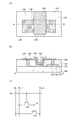
図1(A)は、半導体記憶装置である不揮発性メモリの上面図である。図1(A)における一点鎖線A−Bに対応する断面A−Bを図1(B)に示す。ただし、簡単のため、図1(A)では絶縁膜108を省略して示す。
FIG. 1A is a top view of a nonvolatile memory which is a semiconductor memory device. FIG. 1B shows a cross section AB corresponding to the one-dot chain line AB in FIG. However, for simplicity, the
図1(C)は、不揮発性メモリの回路構成を示す。不揮発性メモリは、オフ電流が極めて小さいトランジスタ150と、トランジスタ150のゲートと接続するゲート配線GLと、トランジスタ150のソースと接続するソース配線SL_1と、トランジスタ170と、トランジスタ170のソースと接続するソース配線SL_2と、トランジスタ170のドレインと接続するドレイン配線DLと、キャパシタ160と、キャパシタ160の一端と接続する容量配線CLと、キャパシタ160の他端、トランジスタ150のドレインおよびトランジスタ170のゲートと接続するノードNと、を有する。
FIG. 1C illustrates a circuit configuration of the nonvolatile memory. The nonvolatile memory includes a
なお、本実施の形態に示す不揮発性メモリは、ノードNの電圧に応じて、トランジスタ170のしきい値電圧が変動することを利用したものである。例えば、図1(D)は容量配線CLの電圧VCLと、トランジスタ170を流れるドレイン電流Idsとの関係を説明する図である。
Note that the nonvolatile memory described in this embodiment utilizes the fact that the threshold voltage of the
ここで、トランジスタ150を介して、ノードNの電圧を調整することができる。例えば、ソース配線SL_1の電圧をVDDとする。このとき、ゲート配線GLの電圧をトランジスタ150のしきい値電圧VthにVDDを加えた電圧以上とすることで、ノードNの電圧をN=HIGHにすることができる。また、ゲート配線GLの電圧をトランジスタ150のしきい値電圧Vth以下とすることで、ノードNの電圧をN=LOWにすることができる。
Here, the voltage of the node N can be adjusted through the
そのため、N=LOWで示したVCL−Idsカーブと、N=HIGHで示したVCL−Idsカーブのいずれかを得ることができる。即ち、N=LOWでは、VCL=0VにてIdsが小さいため、データ0となる。また、N=HIGHでは、VCL=0VにてIdsが大きいため、データ1となる。このようにして、データを記憶することができる。 Therefore, it is possible to obtain a V CL -Ids curve indicated by N = LOW, one of V CL -Ids curve indicated by N = HIGH. That is, when N = LOW, the data becomes 0 because Ids is small at V CL = 0V. Further, when N = HIGH, data 1 is obtained because Ids is large when V CL = 0V. In this way, data can be stored.
ここで、トランジスタ150にオフ電流が極めて小さいトランジスタを適用することで、ノードNに蓄積された電荷がトランジスタ150を通して意図せずにリークすることを抑制できる。そのため、長期間に渡ってデータを保持することができる。
Here, by applying a transistor with an extremely small off-state current to the
次に、本発明の一形態である不揮発性メモリを構成するトランジスタおよびキャパシタの構造について、図1(B)に示す断面A−Bを用いて説明する。 Next, structures of a transistor and a capacitor included in the nonvolatile memory which is one embodiment of the present invention are described with reference to a cross section AB of FIG.
半導体記憶装置は、基板100と、基板100上の半導体膜126と、半導体膜126を覆う絶縁膜128と、絶縁膜128を介して半導体膜126上に設けられた導電膜124と、絶縁膜128上にあり半導体膜126と重畳しない、導電膜124と同一層かつ同一材料である導電膜125と、絶縁膜128上にあり、導電膜124および導電膜125の上面を露出し、絶縁膜128を露出する溝部を有する絶縁膜120と、絶縁膜120上にあり、絶縁膜120の溝部の側面および底面(絶縁膜128)、導電膜124ならびに導電膜125と接する酸化物半導体膜106と、酸化物半導体膜106を覆う絶縁膜108と、絶縁膜108を介して酸化物半導体膜106および絶縁膜120の溝部上に設けられた導電膜104と、絶縁膜108および酸化物半導体膜106を介して導電膜124と重畳する、導電膜104と同一層かつ同一材料である導電膜105と、を有する。
The semiconductor memory device includes a
なお、絶縁膜120に設けられた溝部は絶縁膜128ではなく基板100を露出しても構わない。また、溝部は、導電膜124と導電膜125との間に設けられる。
Note that the groove provided in the insulating
ここで、トランジスタ150において、導電膜124はソース電極またはドレイン電極の一方として機能する。また、導電膜125はソース電極またはドレイン電極の他方として機能する。また、酸化物半導体膜106はチャネル領域を有する。また、絶縁膜108は、ゲート絶縁膜として機能する。また、導電膜104はゲート電極として機能する。
Here, in the
このとき、チャネル領域を有する酸化物半導体膜106が、絶縁膜120の溝部に接して設けられるため、上面から見たソース電極およびドレイン電極(導電膜124および導電膜125)間距離である見かけ上のチャネル長L(図1(A)参照。)に対して、断面から見たチャネル領域(酸化物半導体膜106)におけるチャネル領域の長さである実効上のチャネル長L’(図1(B)参照。)を長くすることができる。例えば、絶縁膜120に設けられる溝部の深さを、上面から見た導電膜124および導電膜125間距離の二分の一以上にすれば、見かけ上のチャネル長Lに対する実効上のチャネル長L’の長さを2倍以上にすることができる。好ましくは、見かけ上のチャネル長Lに対する実効上のチャネル長L’の長さを3倍以上、さらに好ましくは4倍以上とするように絶縁膜120の厚さおよび溝部の深さを選択する。例えば、見かけ上のチャネル長Lが15nm以上100nm以下の範囲の場合、絶縁膜120に設けられる溝部の深さは7.5nm以上200nm以下とすればよい。絶縁膜120に設けられる溝部の深さは前述の範囲に限定されない。ただし、酸化物半導体膜106の厚さを溝部の深さよりも薄くしなければ、見かけ上のチャネル長Lに対して、実効上のチャネル長L’を長くすることができないことは述べるまでもない。そのため、溝部の深さは酸化物半導体膜106の厚さ以上とする。
At this time, since the
絶縁膜120に設けられた溝部は絶縁膜128または基板100を露出するとしているが、これに限定されない。例えば、絶縁膜120中に溝部の底面を有していてもよい。また、絶縁膜128または基板100上にエッチストップ膜を別途設け、該エッチストップ膜を露出してもよい。
Although the groove provided in the insulating
キャパシタ160の構成は以下の通りである。導電膜124は第1の容量電極として機能する。絶縁膜108は、誘電体膜として機能する。導電膜105は第2の容量電極として機能する。
The configuration of the
トランジスタ170の構成は以下の通りである。導電膜124はゲート電極として機能する。また、半導体膜126はチャネル領域を有する。また、絶縁膜128は、ゲート絶縁膜として機能する。図示しないが、半導体膜126において、少なくとも導電膜124と重畳しない領域に、半導体膜126に設けられるチャネル領域よりも低抵抗であるソース領域およびドレイン領域を設ける。また、ソース領域およびドレイン領域と接し、導電膜124および導電膜125とは異なる層であるソース配線SL_2およびドレイン配線DLを有する。また、ソース領域およびドレイン領域に加えて、チャネル領域よりも抵抗が低く、ソース領域およびドレイン領域よりも抵抗の高いLDD(Lightly Doped Drain)領域を設けてもよい。LDD領域を設けることにより、チャネル長が小さくなると生じるホットキャリア劣化などのトランジスタの劣化を低減することができ、さらに短チャネル効果を低減することができる。
The structure of the
基板100に大きな制限はないが、少なくとも、後の熱処理に耐えうる程度の耐熱性を有している必要がある。例えば、ガラス基板、セラミック基板、石英基板、サファイア基板などを、基板100として用いてもよい。また、シリコンや炭化シリコンなどの単結晶半導体基板、多結晶半導体基板、シリコンゲルマニウムなどの化合物半導体基板、SOI(Silicon On Insulator)基板などを適用することも可能であり、これらの基板上に半導体素子が設けられたものを、基板100として用いてもよい。また、該半導体素子をトランジスタ170に代えても構わない。
There is no particular limitation on the
基板100として、可とう性基板を用いてもよい。その場合は、可とう性基板上に直接的にトランジスタを作製する。なお、可とう性基板上にトランジスタを設ける方法としては、非可とう性の基板上にトランジスタを作製した後、トランジスタを剥離し、可とう性基板である基板100に転置する方法もある。その場合には、非可とう性基板とトランジスタとの間に剥離層を設けるとよい。
A flexible substrate may be used as the
半導体膜126は、非晶質シリコン、微結晶シリコン、多結晶シリコンもしくは単結晶シリコンなどのシリコン系材料、ゲルマニウム系材料、シリコンゲルマニウム系材料、ガリウムヒ素系材料または炭素系材料などを用いればよい。
The
導電膜124、導電膜125、導電膜104および導電膜105は、Al、Ti、Cr、Co、Ni、Cu、Y、Zr、Mo、Ag、TaおよびW、それらの窒化物、酸化物ならびに合金から一以上選択し、単層でまたは積層で用いればよい。また、導電膜104として酸化物を用いる場合は、5×1019cm−3以上20atomic%以下、または1×1020cm−3以上7atomic%以下の窒素を含んでもよい。例えば、1×1020cm−3以上7atomic%以下の窒素を含み、かつIn、GaおよびZnを含む酸化物膜を用いるとよい。酸化物膜を導電膜104に用いる場合、酸化物膜は金属膜と比べて抵抗が高いため、ゲート電極全体の抵抗を低減するために、シート抵抗が10Ω/sq以下の低抵抗膜を積層して設けると好ましい。なお、単位がcm−3で示す濃度はSIMS(Secondary Ion Mass Spectrometry)分析によって定量化でき、単位がatomic%の濃度はXPS(X−ray Photoelectron Spectroscopy)分析によって定量化できる。
The
酸化物半導体膜106は、6nm以上100nm以下、好ましくは15nm以上40nm以下とする。トランジスタ150のチャネル長を小さくすると、スケーリング則に従い、酸化物半導体膜106の厚さを薄くしていくことが好ましい。しかしながら、本発明の一態様を適用することによって、見かけ上のチャネル長Lが短いまま実効上のチャネル長L’を長くすることができるため、前述の範囲の厚さとすることが可能となる。
The
酸化物半導体膜106は、スパッタリング法、プラズマCVD法、PLD(Pulse Laser Deposition)法、MBE(Molecular Beam Epitaxy)法または蒸着法などを用い、例えば、In、Ga、ZnおよびSnから選ばれた二種以上を含む材料を用いればよい。
The
酸化物半導体膜106として、例えば、四元系金属酸化物であるIn−Sn−Ga−Zn−O系の材料や、三元系金属酸化物であるIn−Ga−Zn−O系の材料、In−Sn−Zn−O系の材料、In−Al−Zn−O系の材料、Sn−Ga−Zn−O系の材料、Al−Ga−Zn−O系の材料、Sn−Al−Zn−O系の材料や、二元系金属酸化物であるIn−Zn−O系の材料、Sn−Zn−O系の材料、Al−Zn−O系の材料、Zn−Mg−O系の材料、Sn−Mg−O系の材料、In−Mg−O系の材料、In−Ga−O系の材料や、In−O系の材料、Sn−O系の材料、Zn−O系の材料などを用いればよい。ここで、例えば、In−Ga−Zn−O系の材料とは、インジウム(In)、ガリウム(Ga)、亜鉛(Zn)を有する酸化物、という意味であり、その組成比は特に問わない。また、InとGaとZn以外の元素を含んでいてもよい。このとき、酸化物半導体膜106の化学量論比に対し、Oを過剰にすると好ましい。Oを過剰にすることで酸化物半導体膜106の酸素欠損に起因するキャリアの生成を抑制することができる。
As the
なお、一例として、酸化物半導体膜106としてIn−Zn−O系の材料を用いる場合、原子数比で、In/Zn=0.5以上50以下、好ましくはIn/Zn=1以上20以下、さらに好ましくはIn/Zn=1.5以上15以下とする。Znの原子数比を前述の範囲とすることで、トランジスタの電界効果移動度を向上させることができる。ここで、化合物の原子数比がIn:Zn:O=X:Y:Zのとき、Z>1.5X+Yとすると好ましい。
Note that as an example, when an In—Zn—O-based material is used for the
酸化物半導体膜106として、化学式InMO3(ZnO)m(m>0)で表記される材料を用いてもよい。ここで、Mは、Ga、Al、MnおよびCoから選ばれた一または複数の金属元素を示す。例えば、Mとして、Ga、GaおよびAl、GaおよびMnまたはGaおよびCoなどを用いてもよい。
As the
酸化物半導体膜106は、バンドギャップが2.5eV以上、好ましくは3.0eV以上の材料を選択する。バンドギャップが大きいことにより、熱などによる価電子帯から伝導帯へのキャリアの励起が少なく、該キャリアの励起に起因する電流が生じにくい。加えて、酸化物半導体膜106中に準位を形成する不純物などが少ないと好ましい。
For the
ここで、酸化物半導体膜106は、水素、アルカリ金属およびアルカリ土類金属などが低減され、極めて不純物濃度の低い酸化物半導体膜である。そのため、酸化物半導体膜106をチャネル領域に用いたトランジスタはオフ電流を小さくできる。
Here, the
酸化物半導体膜106中の水素濃度は、5×1018cm−3未満、好ましくは1×1018cm−3以下、より好ましくは5×1017cm−3以下、さらに好ましくは1×1016cm−3以下とする。
The hydrogen concentration in the
アルカリ金属は酸化物半導体を構成する元素ではないため、不純物である。アルカリ土類金属も、酸化物半導体を構成する元素ではない場合において、不純物となる。特に、アルカリ金属のうちナトリウム(Na)は、酸化物半導体膜に接する絶縁膜において、当該絶縁膜中に拡散してNa+となる。また、Naは、酸化物半導体膜内において、酸化物半導体を構成する金属と酸素の結合を分断する、または、その結合中に割り込む。その結果、例えば、しきい値電圧がマイナス方向にシフトすることによるノーマリオン化、電界効果移動度の低下などの、トランジスタ特性の劣化が起こり、加えて、特性のばらつきも生じる。この不純物によりもたらされるトランジスタ特性の劣化と、特性のばらつきは、酸化物半導体膜中の水素濃度が十分に低い場合において顕著に現れる。従って、酸化物半導体膜中の水素濃度が1×1018cm−3以下、または1×1017cm−3以下である場合には、上記不純物の濃度を低減することが望ましい。具体的に、Na濃度の測定値は、5×1016cm−3以下、好ましくは1×1016cm−3以下、さらに好ましくは1×1015cm−3以下とする。同様に、リチウム(Li)濃度の測定値は、5×1015cm−3以下、好ましくは1×1015cm−3以下とする。同様に、カリウム(K)濃度の測定値は、5×1015cm−3以下、好ましくは1×1015cm−3以下とする。 An alkali metal is an impurity because it is not an element included in an oxide semiconductor. Alkaline earth metal is also an impurity when it is not an element constituting an oxide semiconductor. In particular, sodium (Na) among alkali metals diffuses into the insulating film and becomes Na + in the insulating film in contact with the oxide semiconductor film. In the oxide semiconductor film, Na breaks or interrupts the bond between the metal and the oxygen included in the oxide semiconductor. As a result, for example, the transistor characteristics are deteriorated such as a normally-on state due to a shift of the threshold voltage in the negative direction and a reduction in field-effect mobility. In addition, variations in characteristics also occur. The deterioration in transistor characteristics and the variation in characteristics caused by the impurities are noticeable when the hydrogen concentration in the oxide semiconductor film is sufficiently low. Therefore, when the hydrogen concentration in the oxide semiconductor film is 1 × 10 18 cm −3 or less, or 1 × 10 17 cm −3 or less, the concentration of the impurity is preferably reduced. Specifically, the measured value of Na concentration is 5 × 10 16 cm −3 or less, preferably 1 × 10 16 cm −3 or less, and more preferably 1 × 10 15 cm −3 or less. Similarly, the measured value of the lithium (Li) concentration is 5 × 10 15 cm −3 or less, preferably 1 × 10 15 cm −3 or less. Similarly, the measured value of the potassium (K) concentration is 5 × 10 15 cm −3 or less, preferably 1 × 10 15 cm −3 or less.
以上に示した酸化物半導体膜106をトランジスタのチャネル領域に用いることでトランジスタのオフ電流を小さくできる。具体的には、酸化物半導体膜106を用いることにより、例えば、チャネル長が3μm、チャネル幅が1μmのときのトランジスタのオフ電流を1×10⁻¹⁸A以下、または1×10⁻²¹A以下、または1×10⁻²⁴A以下とすることができる。
The off-state current of the transistor can be reduced by using the
酸化物半導体膜106は、単結晶、多結晶(ポリクリスタルともいう。)または非晶質などの状態をとる。
The
好ましくは、酸化物半導体膜106は、CAAC−OS(C Axis Aligned Crystalline Oxide Semiconductor)膜とする。
The
CAAC−OS膜は、完全な単結晶ではなく、完全な非晶質でもない。CAAC−OS膜は、非晶質相に結晶部および非晶質部を有する結晶−非晶質混相構造の酸化物半導体膜である。なお、当該結晶部は、一辺が100nm未満の立方体内に収まる大きさであることが多い。また、透過型電子顕微鏡(TEM:Transmission Electron Microscope)による観察像では、CAAC−OS膜に含まれる非晶質部と結晶部との境界は明確ではない。また、TEMによってCAAC−OS膜には粒界(グレインバウンダリーともいう。)は確認できない。そのため、CAAC−OS膜は、粒界に起因する電子移動度の低下が抑制される。 The CAAC-OS film is not completely single crystal nor completely amorphous. The CAAC-OS film is an oxide semiconductor film with a crystal-amorphous mixed phase structure where crystal parts and amorphous parts are included in an amorphous phase. Note that the crystal part is often large enough to fit in a cube whose one side is less than 100 nm. Further, in the observation image obtained by a transmission electron microscope (TEM), the boundary between the amorphous part and the crystal part included in the CAAC-OS film is not clear. Further, a grain boundary (also referred to as a grain boundary) cannot be confirmed in the CAAC-OS film by TEM. Therefore, in the CAAC-OS film, reduction in electron mobility due to grain boundaries is suppressed.
CAAC−OS膜に含まれる結晶部は、c軸がCAAC−OS膜の被形成面の法線ベクトルまたは表面の法線ベクトルに平行な方向に揃い、かつab面に垂直な方向から見て三角形状または六角形状の原子配列を有し、c軸に垂直な方向から見て金属原子が層状または金属原子と酸素原子とが層状に配列している。なお、異なる結晶部間で、それぞれa軸およびb軸の向きが異なっていてもよい。本明細書において、単に垂直と記載する場合、85°以上95°以下の範囲も含まれることとする。また、単に平行と記載する場合、−5°以上5°以下の範囲も含まれることとする。 In the crystal part included in the CAAC-OS film, the c-axis is aligned in a direction parallel to the normal vector of the formation surface of the CAAC-OS film or the normal vector of the surface, and triangular when viewed from the direction perpendicular to the ab plane. It has a shape or hexagonal atomic arrangement, and metal atoms are arranged in layers or metal atoms and oxygen atoms are arranged in layers as viewed from the direction perpendicular to the c-axis. Note that the directions of the a-axis and the b-axis may be different between different crystal parts. In this specification, a simple term “perpendicular” includes a range from 85 ° to 95 °. In addition, a simple term “parallel” includes a range from −5 ° to 5 °.
なお、CAAC−OS膜において、結晶部の分布が一様でなくてもよい。例えば、CAAC−OS膜の形成過程において、酸化物半導体膜の表面側から結晶成長させる場合、被形成面の近傍に対し表面の近傍では結晶部の占める割合が高くなることがある。また、CAAC−OS膜へ不純物を添加することにより、当該不純物添加領域において結晶部が非晶質化することもある。 Note that the distribution of crystal parts in the CAAC-OS film is not necessarily uniform. For example, in the formation process of the CAAC-OS film, when crystal growth is performed from the surface side of the oxide semiconductor film, the ratio of crystal parts in the vicinity of the surface of the oxide semiconductor film is higher in the vicinity of the surface. In addition, when an impurity is added to the CAAC-OS film, the crystal part in a region to which the impurity is added becomes amorphous in some cases.
CAAC−OS膜に含まれる結晶部のc軸は、CAAC−OS膜の被形成面の法線ベクトルまたは表面の法線ベクトルに平行な方向に揃うため、CAAC−OS膜の形状(被形成面の断面形状または表面の断面形状)によっては互いに異なる方向を向くことがある。なお、結晶部のc軸の方向は、CAAC−OS膜が形成されたときの被形成面の法線ベクトルまたは表面の法線ベクトルに平行な方向となる。結晶部は、成膜することにより、または成膜後に加熱処理などの結晶化処理を行うことにより形成される。 Since the c-axis of the crystal part included in the CAAC-OS film is aligned in a direction parallel to the normal vector of the formation surface of the CAAC-OS film or the normal vector of the surface, the shape of the CAAC-OS film (formation surface) Depending on the cross-sectional shape of the surface or the cross-sectional shape of the surface). Note that the c-axis direction of the crystal part is parallel to the normal vector of the surface where the CAAC-OS film is formed or the normal vector of the surface. The crystal part is formed by film formation or by performing crystallization treatment such as heat treatment after film formation.
CAAC−OS膜を用いたトランジスタは、可視光や紫外光の照射による電気特性の変動を低減することが可能である。よって、当該トランジスタは、信頼性が高い。 A transistor including a CAAC-OS film can reduce variation in electrical characteristics due to irradiation with visible light or ultraviolet light. Therefore, the transistor has high reliability.
絶縁膜108は、等価酸化膜厚換算(酸化シリコン膜厚換算)で0.5nm以上50nm以下、好ましくは5nm以上30nm以下とする。トランジスタ150のチャネル長を小さくすると、スケーリング則に従い、絶縁膜108の厚さを薄くしていくことが好ましい。しかしながら、本発明の一態様を適用することによって、見かけ上のチャネル長Lが短いまま実効上のチャネル長L’を長くすることができるため、前述の範囲の厚さとすることが可能となる。
The insulating
絶縁膜128、絶縁膜120および絶縁膜108は、例えば酸化シリコン、酸化窒化シリコン、窒化酸化シリコン、窒化シリコン、酸化アルミニウム、酸化ハフニウム、酸化イットリウムまたは酸化ジルコニウムなどを用いればよく、積層または単層で設ける。例えば、熱酸化法、プラズマCVD法、スパッタリング法などで形成すればよい。
The insulating
絶縁膜128は、絶縁膜120を加工する際にエッチストップ膜としての機能を有すると好ましい。そのため、絶縁膜128と絶縁膜120とは、加工の際に選択比がとれる材料を選択することが好ましい。例えば、絶縁膜128として酸化シリコン膜を用い、絶縁膜120として窒化シリコン膜を用いるなど、異なる材料とすればよい。
The insulating
絶縁膜128、絶縁膜120および絶縁膜108は、加熱処理により酸素を放出する膜を用いると好ましい。加熱処理により酸素を放出する膜を用いることで、酸化物半導体膜106および酸化物半導体膜106の界面近傍に生じる欠陥を修復することができ、トランジスタの電気特性の劣化を抑制できる。
As the insulating
「加熱処理により酸素を放出する」とは、TDS(Thermal Desorption Spectroscopy:昇温脱離ガス分光法)分析にて、酸素原子に換算しての酸素の放出量が1.0×10¹⁸atoms/cm3以上、または3.0×1020atoms/cm3以上であることをいう。 “Release oxygen by heat treatment” means that the amount of released oxygen converted to oxygen atoms is 1.0 × 10 18 atoms / in TDS (Thermal Desorption Spectroscopy) analysis. It means cm 3 or more, or 3.0 × 10 20 atoms / cm 3 or more.
ここで、TDS分析にて、酸素原子に換算しての酸素の放出量の測定方法について、以下に説明する。 Here, a method for measuring the amount of released oxygen converted into oxygen atoms in TDS analysis will be described below.
TDS分析したときの気体の放出量は、所定の温度範囲におけるイオン強度の積分値に比例する。このため、測定したイオン強度の積分値と、標準試料の基準値との比により、気体の放出量を計算することができる。標準試料の基準値とは、所定の原子を含む試料において、所定の原子に相当するイオン強度の積分値に対する所定の原子の密度の割合である。 The amount of gas released when TDS analysis is performed is proportional to the integral value of ion intensity in a predetermined temperature range. For this reason, the amount of released gas can be calculated from the ratio between the integrated value of the measured ion intensity and the reference value of the standard sample. The reference value of the standard sample is a ratio of the density of the predetermined atom to the integral value of the ion intensity corresponding to the predetermined atom in the sample including the predetermined atom.
例えば、標準試料である所定の密度の水素を含むシリコンウェハのTDS分析結果、および絶縁膜のTDS分析結果から、絶縁膜の酸素分子の放出量(NO2)は、数式1で求めることができる。ここで、TDS分析で得られる質量数32で検出されるガスの全てが酸素分子由来と仮定する。質量数32のものとしてほかにCH3OHがあるが、存在する可能性が低いものとしてここでは考慮しない。また、酸素原子の同位体である質量数17の酸素原子および質量数18の酸素原子を含む酸素分子についても、自然界における存在比率が極微量であるため考慮しない。 For example, the amount of released oxygen molecules (N O2 ) of the insulating film can be obtained from Equation 1 from the TDS analysis result of a silicon wafer containing hydrogen of a predetermined density as a standard sample and the TDS analysis result of the insulating film. . Here, it is assumed that all the gases detected by the mass number 32 obtained by the TDS analysis are derived from oxygen molecules. There is CH 3 OH in addition to those having a mass number of 32, but these are not considered here because they are unlikely to exist. In addition, oxygen molecules containing oxygen atoms with a mass number of 17 and oxygen atoms with a mass number of 18 which are isotopes of oxygen atoms are not considered because the existence ratio in nature is extremely small.
NO2=NH2/SH2×SO2×α (数式1) N O2 = N H2 / S H2 × S O2 × α (Formula 1)
NH2は、標準試料から脱離した水素分子を密度で換算した値である。SH2は、標準試料をTDS分析したときのイオン強度の積分値である。ここで、標準試料の基準値を、NH2/SH2とする。SO2は、絶縁膜をTDS分析したときのイオン強度の積分値である。αは、TDS分析におけるイオン強度に影響する係数である。数式1の詳細に関しては、特開平6−275697公報を参照する。なお、上記絶縁膜の酸素の放出量は、電子科学株式会社製の昇温脱離分析装置EMD−WA1000S/Wを用い、標準試料として1×1016atoms/cm3の水素原子を含むシリコンウェハを用いて測定した。 N H2 is a value obtained by converting hydrogen molecules desorbed from the standard sample by density. SH2 is an integral value of ion intensity when the standard sample is subjected to TDS analysis. Here, the reference value of the standard sample is N H2 / SH 2 . S O2 is an integral value of ion intensity when the insulating film is subjected to TDS analysis. α is a coefficient that affects the ionic strength in the TDS analysis. For details of Equation 1, refer to Japanese Patent Laid-Open No. Hei 6-275697. The oxygen release amount of the insulating film is a silicon wafer containing 1 × 10 16 atoms / cm 3 hydrogen atoms as a standard sample using a temperature programmed desorption analyzer EMD-WA1000S / W manufactured by Electronic Science Co., Ltd. It measured using.
また、TDS分析において、酸素の一部は酸素原子として検出される。酸素分子と酸素原子の比率は、酸素分子のイオン化率から算出することができる。なお、上述のαは酸素分子のイオン化率を含むため、酸素分子の放出量を評価することで、酸素原子の放出量について見積もることができる。 In TDS analysis, part of oxygen is detected as oxygen atoms. The ratio of oxygen molecules to oxygen atoms can be calculated from the ionization rate of oxygen molecules. Note that since the above α includes the ionization rate of oxygen molecules, the amount of oxygen atoms released can be estimated by evaluating the amount of oxygen molecules released.
なお、NO2は酸素分子の放出量である。酸素原子に換算したときの放出量は、酸素分子の放出量の2倍となる。 Note that N 2 O 2 is the amount of released oxygen molecules. The amount of release when converted to oxygen atoms is twice the amount of release of oxygen molecules.
上記構成において、加熱処理により酸素を放出する膜は、酸素が過剰な酸化シリコン(SiOX(X>2))であってもよい。酸素が過剰な酸化シリコン(SiOX(X>2))とは、シリコン原子数の2倍より多い酸素原子を単位体積当たりに含むものである。単位体積当たりのシリコン原子数および酸素原子数は、ラザフォード後方散乱法により測定した値である。 In the above structure, the film from which oxygen is released by heat treatment may be oxygen-excess silicon oxide (SiO X (X> 2)). Oxygen-excess silicon oxide (SiO X (X> 2)) contains oxygen atoms more than twice the number of silicon atoms per unit volume. The numbers of silicon atoms and oxygen atoms per unit volume are values measured by Rutherford backscattering method.
絶縁膜128、絶縁膜120および絶縁膜108から酸化物半導体膜106に酸素が供給されることで、酸化物半導体膜106と絶縁膜128との界面準位密度、酸化物半導体膜106と絶縁膜120との界面準位密度、または酸化物半導体膜106と絶縁膜108との界面準位密度を低減できる。この結果、トランジスタの動作などに起因して、酸化物半導体膜106と絶縁膜128との界面、酸化物半導体膜106と絶縁膜120との界面、または酸化物半導体膜106と絶縁膜108との界面にキャリアが捕獲されることを抑制することができ、良好な電気特性のトランジスタを得ることができる。
When oxygen is supplied from the insulating
さらに、酸化物半導体膜106の酸素欠損に起因して電荷が生じる場合がある。一般に酸化物半導体膜の酸素欠損は、一部がドナーとなりキャリアである電子を放出する。この結果、トランジスタのしきい値電圧がマイナス方向にシフトしてしまう。絶縁膜128、絶縁膜120および絶縁膜108から酸化物半導体膜106に酸素が十分に供給されることにより、しきい値電圧がマイナス方向へシフトする要因である、酸化物半導体膜の酸素欠損を低減することができる。
Further, charge may be generated due to oxygen vacancies in the
以上のようにして得られたトランジスタ150は、酸化物半導体膜106を用いることにより、オフ電流を低減できるため、キャパシタ160に蓄積された電荷を長期間に渡って保持することが可能な不揮発性メモリを提供することができる。また、トランジスタ150は、動作頻度が低くなるため電気特性の劣化が少なく、信頼性の高い不揮発性メモリを提供することができる。
The
また、絶縁膜120に溝部を設け、該溝部と接する酸化物半導体膜106を形成することによって、上面図で見る導電膜124および導電膜125間距離である見かけ上のチャネル長Lに対し、実効上のチャネル長L’を2倍以上、好ましくは3倍以上、さらに好ましくは4倍以上の長さとすることができる。そのため、トランジスタ150のサイズを縮小しても短チャネル効果の影響を低減することが可能となり、不揮発性メモリの集積度を高めることが可能となる。
In addition, by providing a groove in the insulating
次に、図1に示した不揮発性メモリにおいて、キャパシタを含まない構成について図2を用いて説明する。 Next, a configuration in which the capacitor is not included in the nonvolatile memory illustrated in FIG. 1 will be described with reference to FIG.
図2(C)は、不揮発性メモリの回路図である。不揮発性メモリは、トランジスタ150と、トランジスタ150のゲートと接続するゲート配線GLと、トランジスタ150のソースと接続するソース配線SL_1と、トランジスタ170と、トランジスタ170のソースと接続するソース配線SL_2と、トランジスタ170のドレインと接続するドレイン配線DLと、トランジスタ150のドレインとトランジスタ170のゲートと接続するノードNと、を有する。
FIG. 2C is a circuit diagram of the nonvolatile memory. The nonvolatile memory includes a
トランジスタ150にオフ電流の小さなトランジスタを用いる場合、キャパシタを設けなくてもトランジスタ150のドレインとトランジスタ170のゲートの間のノードNに電荷を保持できる。キャパシタを設けない構成であるため、容量配線などが省略されることで小面積化が可能となる。そのため、キャパシタを設けた場合と比べさらに集積度を高めることができる。
In the case where a transistor with a low off-state current is used as the
また、本実施の形態では、配線を4本または5本用いる不揮発性メモリを示したが、これに限定されるものではない。例えば、ソース配線SL_1とドレイン配線DLを共通にする構成としても構わない。 In this embodiment mode, a nonvolatile memory using four or five wirings is shown. However, the present invention is not limited to this. For example, the source wiring SL_1 and the drain wiring DL may be shared.
なお、本実施の形態で示した不揮発性メモリを複数組み合わせて集積化し、メモリセルアレイを作製してもよい。その場合、適宜アドレス線などを追加する。本実施の形態で示した不揮発性メモリを適用することにより、メモリセルアレイの集積度を高めることができる。 Note that a memory cell array may be manufactured by combining a plurality of nonvolatile memories described in this embodiment. In that case, an address line or the like is added as appropriate. By applying the nonvolatile memory described in this embodiment, the degree of integration of the memory cell array can be increased.
次に、本実施の形態に示すトランジスタ150、キャパシタ160およびトランジスタ170を作製する方法の一例について、図3を用いて説明する。
Next, an example of a method for manufacturing the
まず、基板100上に半導体膜126を形成する。次に、絶縁膜128を成膜する(図3(A)参照。)。
First, the
次に、導電膜124および導電膜125を形成する。(図3(B)参照。)。なお、この後、導電膜124をマスクに用いて、半導体膜126に対し、キャリアを生成する不純物(シリコン系の材料の場合、リン、ヒ素、ボロンなど)をイオン注入またはイオンドーピングにより添加してもよい。半導体膜126に不純物を添加することにより、ソース領域およびドレイン領域、またはLDD領域を設けることができる。
Next, the
次に、絶縁膜120を形成する(図3(C)参照。)。絶縁膜120は、絶縁膜を成膜した後、化学的機械研磨(CMP:Chemical Mechanical Polishing)またはエッチバックを行い、その後フォトリソグラフィ工程によって絶縁膜128を露出する溝部を設けることによって形成することができる。または、フォトリソグラフィ工程によって絶縁膜128を露出する溝部を形成し、その後CMPまたはエッチバックによって導電膜124および導電膜125を露出して形成することができる。なお、CMPまたはエッチバックによって導電膜124および導電膜125の一部が除去されてもよい。
Next, the insulating
エッチバックとは、凹凸のある膜表面に平坦化膜を形成し、平坦化膜ごと凹凸のある膜に対して異方性の高いエッチング(例えば、ドライエッチング)を行うことで、膜の凹凸を低減する工程をいう。または、単に、全面に形成された膜に対し、被形成面の一部が露出するまで行うエッチング工程をいう。 Etchback is a process for forming unevenness on a film surface with unevenness, and performing highly anisotropic etching (for example, dry etching) on the uneven film with the flattening film. The process to reduce. Alternatively, it simply refers to an etching process performed until a part of a surface to be formed is exposed to a film formed over the entire surface.
次に、酸化物半導体膜を成膜し、フォトリソグラフィ工程によって酸化物半導体膜106を形成する。酸化物半導体膜106の形成前に、逆スパッタリング処理などのプラズマ処理を行い、絶縁膜120の溝部が有する断面形状上の角を、曲面形状に加工すると好ましい。こうすることで、絶縁膜120の溝部における酸化物半導体膜106の被覆性が向上し、トランジスタ150の電気特性上の不良を低減することができる。次に、絶縁膜108を成膜する(図3(D)参照。)。なお、酸化物半導体膜106となる酸化物半導体膜を成膜した後、および絶縁膜108を成膜した後のいずれか一方、または両方の後に熱処理を行っても構わない。熱処理は150℃以上650℃以下、好ましくは250℃以上450℃以下で行う。熱処理を行うことで、絶縁膜128、絶縁膜120または絶縁膜108より酸素が放出され、酸化物半導体膜106中および酸化物半導体膜106の界面近傍の欠陥を低減することができる。なお、この熱処理は、絶縁膜108を成膜した直後に行うことに限定されず、導電膜144を成膜した直後に行ってもよいし、絶縁膜108の成膜以降のどの工程の後に行っても構わない。
Next, an oxide semiconductor film is formed, and the
次に、導電膜144を成膜する(図3(E)参照。)。次に、導電膜144を加工し、酸化物半導体膜106と重畳する導電膜104、および導電膜124と重畳する導電膜105を形成する(図1(B)参照。)。ここで、導電膜104をマスクにして、酸化物半導体膜106に対し、間接的または直接的にキャリアを生成する不純物(水素、ヘリウム、ネオン、アルゴン、クリプトン、キセノン、窒素、リンなど)をイオン注入法またはイオンドーピング法により添加してもよい。酸化物半導体膜106に不純物を添加することにより、ソース領域およびドレイン領域またはLDD領域を設けることができる。
Next, a
以上の工程によって、図1に示すトランジスタ150、キャパシタ160およびトランジスタ170を作製することができる。
Through the above steps, the
なお、図2に示すトランジスタ150およびトランジスタ170を形成するためには、図1(B)に示すトランジスタ作製の工程中、導電膜105を形成しなければよい。
Note that in order to form the
このように、トランジスタ150、キャパシタ160およびトランジスタ170を同時に作製することが可能であるため、不揮発性メモリを作製するためのフォトリソグラフィ工程数を削減することができる。
In this manner, since the
以上により、三次元の形状を適用することで、集積度を高めても短チャネル効果の影響が低減され、かつフォトリソグラフィ工程数の増加を抑えた半導体記憶装置である不揮発性メモリを提供することができる。 As described above, by applying a three-dimensional shape, a nonvolatile memory which is a semiconductor memory device in which the influence of the short channel effect is reduced even when the integration degree is increased and the increase in the number of photolithography processes is suppressed is provided. Can do.
本実施の形態は、他の実施の形態と適宜組み合わせて用いることができる。 This embodiment can be combined with any of the other embodiments as appropriate.
(実施の形態2)
本実施の形態では、実施の形態1を適用した電子機器の例について説明する。
(Embodiment 2)
In this embodiment, examples of electronic devices to which Embodiment 1 is applied will be described.
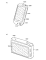
図4(A)は携帯型情報端末である。筐体9300と、ボタン9301と、マイクロフォン9302と、表示部9303と、スピーカ9304と、カメラ9305と、を具備し、携帯型電話機としての機能を有する。本発明の一態様は、携帯型情報端末の内部にあるメモリモジュールに適用することができる。
FIG. 4A illustrates a portable information terminal. A
図4(B)は、デジタルスチルカメラである。筐体9320と、ボタン9321と、マイクロフォン9322と、表示部9323と、を具備する。本発明の一態様は、デジタルスチルカメラの内部にあるメモリモジュールに適用することができる。
FIG. 4B illustrates a digital still camera. A
本発明の一態様を用いることで、電子機器の消費電力を低減でき、また電子機器の価格を安くすることができる。 By using one embodiment of the present invention, power consumption of an electronic device can be reduced and the price of the electronic device can be reduced.
本実施の形態は、他の実施の形態と適宜組み合わせて用いることができる。 This embodiment can be combined with any of the other embodiments as appropriate.
100 基板
104 導電膜
105 導電膜
106 酸化物半導体膜
108 絶縁膜
120 絶縁膜
124 導電膜
125 導電膜
126 半導体膜
128 絶縁膜
144 導電膜
150 トランジスタ
160 キャパシタ
170 トランジスタ
9300 筐体
9301 ボタン
9302 マイクロフォン
9303 表示部
9304 スピーカ
9305 カメラ
9320 筐体
9321 ボタン
9322 マイクロフォン
9323 表示部
100
Claims (5)
前記半導体上方の第1の絶縁膜と、
前記第1の絶縁膜上方の第1の導電膜と、
前記第1の絶縁膜上方の第2の導電膜と、
前記第1の絶縁膜上方に設けられ、前記第1の導電膜と前記第2の導電膜との間に、前記第1の絶縁膜に達する溝部を有する第2の絶縁膜と、
前記第1の導電膜および前記第2の導電膜と接する領域を有し、前記溝部の側面および底面と接する領域を有する酸化物半導体膜と、
前記酸化物半導体膜上方の第3の絶縁膜と、
前記第3の絶縁膜上方の第3の導電膜と、
を有し、
前記第1の導電膜は、前記第1の絶縁膜を介して前記半導体と重なる領域を有し、
前記第3の導電膜は、前記第3の絶縁膜を介して前記酸化物半導体膜と重なる領域を有し、
前記酸化物半導体膜は、前記第1の絶縁膜と接する領域を有することを特徴とする半導体記憶装置。 And semiconductors,
A first insulating layer of the semiconductor body above direction,
A first conductive film above the first insulating film;
A second conductive film above the first insulating film;
A second insulating film provided above the first insulating film and having a groove reaching the first insulating film between the first conductive film and the second conductive film;
An oxide semiconductor film having a region in contact with the first conductive film and the second conductive film, and a region in contact with a side surface and a bottom surface of the groove;
A third insulating film above the oxide semiconductor film;
A third conductive film above the third insulating film;
Have
The first conductive film has a region overlapping with the semiconductor body through said first insulating film,
The third conductive film, have a region overlapping with the oxide semiconductor film through said third insulating film,
The semiconductor memory device , wherein the oxide semiconductor film has a region in contact with the first insulating film .
前記半導体上方の第1の絶縁膜と、
前記第1の絶縁膜上方の第1の導電膜と、
前記第1の絶縁膜上方の第2の導電膜と、
前記第1の絶縁膜上方に設けられ、前記第1の導電膜と前記第2の導電膜との間に、前記第1の絶縁膜に達する溝部を有する第2の絶縁膜と、
前記第1の導電膜および前記第2の導電膜と接する領域を有し、前記溝部の側面および底面と接する領域を有する酸化物半導体膜と、
前記酸化物半導体膜上方の第3の絶縁膜と、
前記第3の絶縁膜上方の第3の導電膜と、
前記第3の絶縁膜上方の第4の導電膜と、
を有し、
前記第1の導電膜は、前記第1の絶縁膜を介して前記半導体と重なる領域を有し、
前記第3の導電膜は、前記第3の絶縁膜を介して前記酸化物半導体膜と重なる領域を有し、
前記第4の導電膜は、前記第3の絶縁膜および前記酸化物半導体膜を介して前記第1の導電膜と重なる領域を有し、
前記酸化物半導体膜は、前記第1の絶縁膜と接する領域を有することを特徴とする半導体記憶装置。 And semiconductors,
A first insulating layer of the semiconductor body above direction,
A first conductive film above the first insulating film;
A second conductive film above the first insulating film;
A second insulating film provided above the first insulating film and having a groove reaching the first insulating film between the first conductive film and the second conductive film;
An oxide semiconductor film having a region in contact with the first conductive film and the second conductive film, and a region in contact with a side surface and a bottom surface of the groove;
A third insulating film above the oxide semiconductor film;
A third conductive film above the third insulating film;
A fourth conductive film above the third insulating film;
Have
The first conductive film has a region overlapping with the semiconductor body through said first insulating film,
The third conductive film has a region overlapping with the oxide semiconductor film with the third insulating film interposed therebetween,
The fourth conductive film, have a region overlapping with the first conductive film through said third insulating film and the oxide semiconductor film,
The semiconductor memory device , wherein the oxide semiconductor film has a region in contact with the first insulating film .
前記第4の導電膜は、前記第3の導電膜と同一材料を有することを特徴とする半導体記憶装置。 In claim 2,
The semiconductor memory device, wherein the fourth conductive film has the same material as the third conductive film.
前記第2の導電膜は、前記第1の導電膜と同一材料を有することを特徴とする半導体記憶装置。 In any one of Claims 1 thru | or 3,
The semiconductor memory device, wherein the second conductive film has the same material as the first conductive film.
前記第2の絶縁膜は、前記第1の導電膜および前記第2の導電膜の上面を露出するように設けられることを特徴とする半導体記憶装置。 In any one of Claims 1 thru | or 4,
The semiconductor memory device, wherein the second insulating film is provided so as to expose upper surfaces of the first conductive film and the second conductive film.
Priority Applications (1)
| Application Number | Priority Date | Filing Date | Title |
|---|---|---|---|
| JP2012048891A JP5961409B2 (en) | 2011-03-10 | 2012-03-06 | Semiconductor memory device |
Applications Claiming Priority (3)
| Application Number | Priority Date | Filing Date | Title |
|---|---|---|---|
| JP2011052270 | 2011-03-10 | ||
| JP2011052270 | 2011-03-10 | ||
| JP2012048891A JP5961409B2 (en) | 2011-03-10 | 2012-03-06 | Semiconductor memory device |
Related Child Applications (1)
| Application Number | Title | Priority Date | Filing Date |
|---|---|---|---|
| JP2016126477A Division JP6197075B2 (en) | 2011-03-10 | 2016-06-27 | Semiconductor device |
Publications (3)
| Publication Number | Publication Date |
|---|---|
| JP2012199536A JP2012199536A (en) | 2012-10-18 |
| JP2012199536A5 JP2012199536A5 (en) | 2015-03-26 |
| JP5961409B2 true JP5961409B2 (en) | 2016-08-02 |
Family
ID=46794749
Family Applications (2)
| Application Number | Title | Priority Date | Filing Date |
|---|---|---|---|
| JP2012048891A Expired - Fee Related JP5961409B2 (en) | 2011-03-10 | 2012-03-06 | Semiconductor memory device |
| JP2016126477A Expired - Fee Related JP6197075B2 (en) | 2011-03-10 | 2016-06-27 | Semiconductor device |
Family Applications After (1)
| Application Number | Title | Priority Date | Filing Date |
|---|---|---|---|
| JP2016126477A Expired - Fee Related JP6197075B2 (en) | 2011-03-10 | 2016-06-27 | Semiconductor device |
Country Status (4)
| Country | Link |
|---|---|
| US (1) | US8772849B2 (en) |
| JP (2) | JP5961409B2 (en) |
| KR (2) | KR101954592B1 (en) |
| TW (1) | TWI550829B (en) |
Families Citing this family (13)
| Publication number | Priority date | Publication date | Assignee | Title |
|---|---|---|---|---|
| KR100753600B1 (en) * | 2007-05-28 | 2007-08-30 | 원철수 | Mounting unit for molding member and appratus for coating molding member using the same |
| US20120298998A1 (en) * | 2011-05-25 | 2012-11-29 | Semiconductor Energy Laboratory Co., Ltd. | Method for forming oxide semiconductor film, semiconductor device, and method for manufacturing semiconductor device |
| WO2013054823A1 (en) * | 2011-10-14 | 2013-04-18 | Semiconductor Energy Laboratory Co., Ltd. | Semiconductor device and manufacturing method thereof |
| US9607991B2 (en) | 2013-09-05 | 2017-03-28 | Semiconductor Energy Laboratory Co., Ltd. | Semiconductor device |
| KR102332469B1 (en) | 2014-03-28 | 2021-11-30 | 가부시키가이샤 한도오따이 에네루기 켄큐쇼 | Transistor and semiconductor device |
| TWI767772B (en) | 2014-04-10 | 2022-06-11 | 日商半導體能源研究所股份有限公司 | Memory device and semiconductor device |
| WO2015170220A1 (en) | 2014-05-09 | 2015-11-12 | Semiconductor Energy Laboratory Co., Ltd. | Memory device and electronic device |
| US10671204B2 (en) | 2015-05-04 | 2020-06-02 | Semiconductor Energy Laboratory Co., Ltd. | Touch panel and data processor |
| US9741400B2 (en) | 2015-11-05 | 2017-08-22 | Semiconductor Energy Laboratory Co., Ltd. | Semiconductor device, memory device, electronic device, and method for operating the semiconductor device |
| US11710790B2 (en) | 2020-05-29 | 2023-07-25 | Taiwan Semiconductor Manufacturing Company, Ltd. | Memory array channel regions |
| US11695073B2 (en) | 2020-05-29 | 2023-07-04 | Taiwan Semiconductor Manufacturing Co., Ltd. | Memory array gate structures |
| US11640974B2 (en) * | 2020-06-30 | 2023-05-02 | Taiwan Semiconductor Manufacturing Co., Ltd. | Memory array isolation structures |
| US11729987B2 (en) | 2020-06-30 | 2023-08-15 | Taiwan Semiconductor Manufacturing Company, Ltd. | Memory array source/drain electrode structures |
Family Cites Families (121)
| Publication number | Priority date | Publication date | Assignee | Title |
|---|---|---|---|---|
| JPS6034199B2 (en) | 1980-12-20 | 1985-08-07 | 株式会社東芝 | semiconductor storage device |
| US5317432A (en) | 1991-09-04 | 1994-05-31 | Sony Corporation | Liquid crystal display device with a capacitor and a thin film transistor in a trench for each pixel |
| JP3287038B2 (en) * | 1991-12-19 | 2002-05-27 | ソニー株式会社 | Liquid crystal display |
| KR950007358B1 (en) * | 1992-07-01 | 1995-07-10 | 현대전자산업주식회사 | Making method of tft with trench surrounding gate structure |
| JP2921812B2 (en) | 1992-12-24 | 1999-07-19 | シャープ株式会社 | Nonvolatile semiconductor memory device |
| JP3209600B2 (en) * | 1992-12-24 | 2001-09-17 | キヤノン株式会社 | Method for manufacturing thin film transistor |
| JP3298974B2 (en) | 1993-03-23 | 2002-07-08 | 電子科学株式会社 | Thermal desorption gas analyzer |
| KR100394896B1 (en) | 1995-08-03 | 2003-11-28 | 코닌클리케 필립스 일렉트로닉스 엔.브이. | A semiconductor device including a transparent switching element |
| JP3625598B2 (en) | 1995-12-30 | 2005-03-02 | 三星電子株式会社 | Manufacturing method of liquid crystal display device |
| JP4170454B2 (en) | 1998-07-24 | 2008-10-22 | Hoya株式会社 | Article having transparent conductive oxide thin film and method for producing the same |
| JP2000150861A (en) | 1998-11-16 | 2000-05-30 | Tdk Corp | Oxide thin film |
| JP3276930B2 (en) | 1998-11-17 | 2002-04-22 | 科学技術振興事業団 | Transistor and semiconductor device |
| TW460731B (en) | 1999-09-03 | 2001-10-21 | Ind Tech Res Inst | Electrode structure and production method of wide viewing angle LCD |
| JP3915868B2 (en) | 2000-07-07 | 2007-05-16 | セイコーエプソン株式会社 | Ferroelectric memory device and manufacturing method thereof |
| JP4089858B2 (en) | 2000-09-01 | 2008-05-28 | 国立大学法人東北大学 | Semiconductor device |
| JP3749101B2 (en) * | 2000-09-14 | 2006-02-22 | 株式会社ルネサステクノロジ | Semiconductor device |
| KR20020038482A (en) | 2000-11-15 | 2002-05-23 | 모리시타 요이찌 | Thin film transistor array, method for producing the same, and display panel using the same |
| JP3997731B2 (en) | 2001-03-19 | 2007-10-24 | 富士ゼロックス株式会社 | Method for forming a crystalline semiconductor thin film on a substrate |
| JP2002289859A (en) | 2001-03-23 | 2002-10-04 | Minolta Co Ltd | Thin-film transistor |
| JP2002368226A (en) | 2001-06-11 | 2002-12-20 | Sharp Corp | Semiconductor device, semiconductor memory device and manufacturing method, and portable information equipment |
| JP4090716B2 (en) | 2001-09-10 | 2008-05-28 | 雅司 川崎 | Thin film transistor and matrix display device |
| JP3925839B2 (en) | 2001-09-10 | 2007-06-06 | シャープ株式会社 | Semiconductor memory device and test method thereof |
| JP4164562B2 (en) | 2002-09-11 | 2008-10-15 | 独立行政法人科学技術振興機構 | Transparent thin film field effect transistor using homologous thin film as active layer |
| EP1443130B1 (en) | 2001-11-05 | 2011-09-28 | Japan Science and Technology Agency | Natural superlattice homologous single crystal thin film, method for preparation thereof, and device using said single crystal thin film |
| JP4083486B2 (en) | 2002-02-21 | 2008-04-30 | 独立行政法人科学技術振興機構 | Method for producing LnCuO (S, Se, Te) single crystal thin film |
| CN1445821A (en) | 2002-03-15 | 2003-10-01 | 三洋电机株式会社 | Forming method of ZnO film and ZnO semiconductor layer, semiconductor element and manufacturing method thereof |
| JP3933591B2 (en) | 2002-03-26 | 2007-06-20 | 淳二 城戸 | Organic electroluminescent device |
| US7339187B2 (en) | 2002-05-21 | 2008-03-04 | State Of Oregon Acting By And Through The Oregon State Board Of Higher Education On Behalf Of Oregon State University | Transistor structures |
| JP2004022625A (en) | 2002-06-13 | 2004-01-22 | Murata Mfg Co Ltd | Manufacturing method of semiconductor device and its manufacturing method |
| US7105868B2 (en) | 2002-06-24 | 2006-09-12 | Cermet, Inc. | High-electron mobility transistor with zinc oxide |
| US7067843B2 (en) | 2002-10-11 | 2006-06-27 | E. I. Du Pont De Nemours And Company | Transparent oxide semiconductor thin film transistors |
| JP4166105B2 (en) | 2003-03-06 | 2008-10-15 | シャープ株式会社 | Semiconductor device and manufacturing method thereof |
| JP2004273732A (en) | 2003-03-07 | 2004-09-30 | Sharp Corp | Active matrix substrate and its producing process |
| JP4108633B2 (en) | 2003-06-20 | 2008-06-25 | シャープ株式会社 | THIN FILM TRANSISTOR, MANUFACTURING METHOD THEREOF, AND ELECTRONIC DEVICE |
| US7262463B2 (en) | 2003-07-25 | 2007-08-28 | Hewlett-Packard Development Company, L.P. | Transistor including a deposited channel region having a doped portion |
| US7282782B2 (en) | 2004-03-12 | 2007-10-16 | Hewlett-Packard Development Company, L.P. | Combined binary oxide semiconductor device |
| US7145174B2 (en) | 2004-03-12 | 2006-12-05 | Hewlett-Packard Development Company, Lp. | Semiconductor device |
| EP2413366B1 (en) | 2004-03-12 | 2017-01-11 | Japan Science And Technology Agency | A switching element of LCDs or organic EL displays |
| US7297977B2 (en) | 2004-03-12 | 2007-11-20 | Hewlett-Packard Development Company, L.P. | Semiconductor device |
| US7211825B2 (en) | 2004-06-14 | 2007-05-01 | Yi-Chi Shih | Indium oxide-based thin film transistors and circuits |
| JP2006049413A (en) | 2004-08-02 | 2006-02-16 | Fujitsu Ltd | Semiconductor device and its manufacturing method |
| JP2006100760A (en) | 2004-09-02 | 2006-04-13 | Casio Comput Co Ltd | Thin-film transistor and its manufacturing method |
| US7285501B2 (en) | 2004-09-17 | 2007-10-23 | Hewlett-Packard Development Company, L.P. | Method of forming a solution processed device |
| JP4143589B2 (en) | 2004-10-15 | 2008-09-03 | エルピーダメモリ株式会社 | Manufacturing method of semiconductor device |
| US7298084B2 (en) | 2004-11-02 | 2007-11-20 | 3M Innovative Properties Company | Methods and displays utilizing integrated zinc oxide row and column drivers in conjunction with organic light emitting diodes |
| US7863611B2 (en) | 2004-11-10 | 2011-01-04 | Canon Kabushiki Kaisha | Integrated circuits utilizing amorphous oxides |
| US7829444B2 (en) | 2004-11-10 | 2010-11-09 | Canon Kabushiki Kaisha | Field effect transistor manufacturing method |
| KR100953596B1 (en) | 2004-11-10 | 2010-04-21 | 캐논 가부시끼가이샤 | Light-emitting device |
| US7453065B2 (en) | 2004-11-10 | 2008-11-18 | Canon Kabushiki Kaisha | Sensor and image pickup device |
| CN101057338B (en) | 2004-11-10 | 2011-03-16 | 佳能株式会社 | Field effect transistor employing an amorphous oxide |
| US7791072B2 (en) | 2004-11-10 | 2010-09-07 | Canon Kabushiki Kaisha | Display |
| CN101057339B (en) | 2004-11-10 | 2012-12-26 | 佳能株式会社 | Amorphous oxide and field effect transistor |
| US7579224B2 (en) | 2005-01-21 | 2009-08-25 | Semiconductor Energy Laboratory Co., Ltd. | Method for manufacturing a thin film semiconductor device |
| TWI472037B (en) | 2005-01-28 | 2015-02-01 | Semiconductor Energy Lab | Semiconductor device, electronic device, and method of manufacturing semiconductor device |
| TWI569441B (en) | 2005-01-28 | 2017-02-01 | 半導體能源研究所股份有限公司 | Semiconductor device, electronic device, and method of manufacturing semiconductor device |
| US7858451B2 (en) | 2005-02-03 | 2010-12-28 | Semiconductor Energy Laboratory Co., Ltd. | Electronic device, semiconductor device and manufacturing method thereof |
| US7948171B2 (en) | 2005-02-18 | 2011-05-24 | Semiconductor Energy Laboratory Co., Ltd. | Light emitting device |
| US20060197092A1 (en) | 2005-03-03 | 2006-09-07 | Randy Hoffman | System and method for forming conductive material on a substrate |
| US8681077B2 (en) | 2005-03-18 | 2014-03-25 | Semiconductor Energy Laboratory Co., Ltd. | Semiconductor device, and display device, driving method and electronic apparatus thereof |
| WO2006105077A2 (en) | 2005-03-28 | 2006-10-05 | Massachusetts Institute Of Technology | Low voltage thin film transistor with high-k dielectric material |
| US7645478B2 (en) | 2005-03-31 | 2010-01-12 | 3M Innovative Properties Company | Methods of making displays |
| US8300031B2 (en) | 2005-04-20 | 2012-10-30 | Semiconductor Energy Laboratory Co., Ltd. | Semiconductor device comprising transistor having gate and drain connected through a current-voltage conversion element |
| JP2006344849A (en) | 2005-06-10 | 2006-12-21 | Casio Comput Co Ltd | Thin film transistor |
| US7402506B2 (en) | 2005-06-16 | 2008-07-22 | Eastman Kodak Company | Methods of making thin film transistors comprising zinc-oxide-based semiconductor materials and transistors made thereby |
| US7691666B2 (en) | 2005-06-16 | 2010-04-06 | Eastman Kodak Company | Methods of making thin film transistors comprising zinc-oxide-based semiconductor materials and transistors made thereby |
| US7507618B2 (en) | 2005-06-27 | 2009-03-24 | 3M Innovative Properties Company | Method for making electronic devices using metal oxide nanoparticles |
| KR100711890B1 (en) | 2005-07-28 | 2007-04-25 | 삼성에스디아이 주식회사 | Organic Light Emitting Display and Fabrication Method for the same |
| JP2007059128A (en) | 2005-08-23 | 2007-03-08 | Canon Inc | Organic electroluminescent display device and manufacturing method thereof |
| JP5116225B2 (en) | 2005-09-06 | 2013-01-09 | キヤノン株式会社 | Manufacturing method of oxide semiconductor device |
| JP4280736B2 (en) | 2005-09-06 | 2009-06-17 | キヤノン株式会社 | Semiconductor element |
| JP4850457B2 (en) | 2005-09-06 | 2012-01-11 | キヤノン株式会社 | Thin film transistor and thin film diode |
| JP2007073705A (en) | 2005-09-06 | 2007-03-22 | Canon Inc | Oxide-semiconductor channel film transistor and its method of manufacturing same |
| EP3614442A3 (en) | 2005-09-29 | 2020-03-25 | Semiconductor Energy Laboratory Co., Ltd. | Semiconductor device having oxide semiconductor layer and manufactoring method thereof |
| JP5037808B2 (en) | 2005-10-20 | 2012-10-03 | キヤノン株式会社 | Field effect transistor using amorphous oxide, and display device using the transistor |
| KR20090115222A (en) | 2005-11-15 | 2009-11-04 | 가부시키가이샤 한도오따이 에네루기 켄큐쇼 | Manufacturing method of semiconductor device |
| TWI292281B (en) | 2005-12-29 | 2008-01-01 | Ind Tech Res Inst | Pixel structure of active organic light emitting diode and method of fabricating the same |
| US7867636B2 (en) | 2006-01-11 | 2011-01-11 | Murata Manufacturing Co., Ltd. | Transparent conductive film and method for manufacturing the same |
| JP4977478B2 (en) | 2006-01-21 | 2012-07-18 | 三星電子株式会社 | ZnO film and method of manufacturing TFT using the same |
| US7576394B2 (en) | 2006-02-02 | 2009-08-18 | Kochi Industrial Promotion Center | Thin film transistor including low resistance conductive thin films and manufacturing method thereof |
| US7977169B2 (en) | 2006-02-15 | 2011-07-12 | Kochi Industrial Promotion Center | Semiconductor device including active layer made of zinc oxide with controlled orientations and manufacturing method thereof |
| JP4935138B2 (en) * | 2006-03-23 | 2012-05-23 | セイコーエプソン株式会社 | Circuit board, circuit board manufacturing method, electro-optical device, and electronic apparatus |
| KR20070101595A (en) | 2006-04-11 | 2007-10-17 | 삼성전자주식회사 | Zno thin film transistor |
| US20070252928A1 (en) | 2006-04-28 | 2007-11-01 | Toppan Printing Co., Ltd. | Structure, transmission type liquid crystal display, reflection type display and manufacturing method thereof |
| JP5028033B2 (en) | 2006-06-13 | 2012-09-19 | キヤノン株式会社 | Oxide semiconductor film dry etching method |
| JP2008004738A (en) | 2006-06-22 | 2008-01-10 | Elpida Memory Inc | Semiconductor device and method of manufacturing the same |
| JP4609797B2 (en) | 2006-08-09 | 2011-01-12 | Nec液晶テクノロジー株式会社 | Thin film device and manufacturing method thereof |
| JP4999400B2 (en) | 2006-08-09 | 2012-08-15 | キヤノン株式会社 | Oxide semiconductor film dry etching method |
| JP4332545B2 (en) | 2006-09-15 | 2009-09-16 | キヤノン株式会社 | Field effect transistor and manufacturing method thereof |
| JP5164357B2 (en) | 2006-09-27 | 2013-03-21 | キヤノン株式会社 | Semiconductor device and manufacturing method of semiconductor device |
| JP4274219B2 (en) | 2006-09-27 | 2009-06-03 | セイコーエプソン株式会社 | Electronic devices, organic electroluminescence devices, organic thin film semiconductor devices |
| US7622371B2 (en) | 2006-10-10 | 2009-11-24 | Hewlett-Packard Development Company, L.P. | Fused nanocrystal thin film semiconductor and method |
| US7772021B2 (en) | 2006-11-29 | 2010-08-10 | Samsung Electronics Co., Ltd. | Flat panel displays comprising a thin-film transistor having a semiconductive oxide in its channel and methods of fabricating the same for use in flat panel displays |
| JP2008140684A (en) | 2006-12-04 | 2008-06-19 | Toppan Printing Co Ltd | Color el display, and its manufacturing method |
| KR101303578B1 (en) | 2007-01-05 | 2013-09-09 | 삼성전자주식회사 | Etching method of thin film |
| US8207063B2 (en) | 2007-01-26 | 2012-06-26 | Eastman Kodak Company | Process for atomic layer deposition |
| KR100851215B1 (en) | 2007-03-14 | 2008-08-07 | 삼성에스디아이 주식회사 | Thin film transistor and organic light-emitting dislplay device having the thin film transistor |
| US7795613B2 (en) | 2007-04-17 | 2010-09-14 | Toppan Printing Co., Ltd. | Structure with transistor |
| KR101325053B1 (en) | 2007-04-18 | 2013-11-05 | 삼성디스플레이 주식회사 | Thin film transistor substrate and manufacturing method thereof |
| KR20080094300A (en) | 2007-04-19 | 2008-10-23 | 삼성전자주식회사 | Thin film transistor and method of manufacturing the same and flat panel display comprising the same |
| KR101334181B1 (en) | 2007-04-20 | 2013-11-28 | 삼성전자주식회사 | Thin Film Transistor having selectively crystallized channel layer and method of manufacturing the same |
| CN101663762B (en) | 2007-04-25 | 2011-09-21 | 佳能株式会社 | Oxynitride semiconductor |
| KR101345376B1 (en) | 2007-05-29 | 2013-12-24 | 삼성전자주식회사 | Fabrication method of ZnO family Thin film transistor |
| JP2009016368A (en) | 2007-06-29 | 2009-01-22 | Ricoh Co Ltd | Memory device |
| JP5430846B2 (en) | 2007-12-03 | 2014-03-05 | 株式会社半導体エネルギー研究所 | Method for manufacturing semiconductor device |
| JP5215158B2 (en) | 2007-12-17 | 2013-06-19 | 富士フイルム株式会社 | Inorganic crystalline alignment film, method for manufacturing the same, and semiconductor device |
| JP5305696B2 (en) | 2008-03-06 | 2013-10-02 | キヤノン株式会社 | Semiconductor device processing method |
| JP2009253249A (en) | 2008-04-11 | 2009-10-29 | Elpida Memory Inc | Semiconductor device, its manufacturing method and data processing system |
| US7893494B2 (en) | 2008-06-18 | 2011-02-22 | International Business Machines Corporation | Method and structure for SOI body contact FET with reduced parasitic capacitance |
| JP4623179B2 (en) | 2008-09-18 | 2011-02-02 | ソニー株式会社 | Thin film transistor and manufacturing method thereof |
| JP5451280B2 (en) | 2008-10-09 | 2014-03-26 | キヤノン株式会社 | Wurtzite crystal growth substrate, manufacturing method thereof, and semiconductor device |
| WO2010071034A1 (en) | 2008-12-19 | 2010-06-24 | Semiconductor Energy Laboratory Co., Ltd. | Method for manufacturing transistor |
| US8461582B2 (en) * | 2009-03-05 | 2013-06-11 | Semiconductor Energy Laboratory Co., Ltd. | Semiconductor device and method for manufacturing the same |
| WO2011007677A1 (en) * | 2009-07-17 | 2011-01-20 | Semiconductor Energy Laboratory Co., Ltd. | Semiconductor device and method for manufacturing the same |
| WO2012002186A1 (en) * | 2010-07-02 | 2012-01-05 | Semiconductor Energy Laboratory Co., Ltd. | Semiconductor device |
| KR101851817B1 (en) * | 2010-09-03 | 2018-04-24 | 가부시키가이샤 한도오따이 에네루기 켄큐쇼 | Semiconductor device and driving method thereof |
| WO2012102182A1 (en) | 2011-01-26 | 2012-08-02 | Semiconductor Energy Laboratory Co., Ltd. | Semiconductor device |
| TWI602303B (en) | 2011-01-26 | 2017-10-11 | 半導體能源研究所股份有限公司 | Semiconductor device and manufacturing method thereof |
| CN103348464B (en) | 2011-01-26 | 2016-01-13 | 株式会社半导体能源研究所 | Semiconductor device and manufacture method thereof |
| US9691772B2 (en) | 2011-03-03 | 2017-06-27 | Semiconductor Energy Laboratory Co., Ltd. | Semiconductor memory device including memory cell which includes transistor and capacitor |
| US8841664B2 (en) * | 2011-03-04 | 2014-09-23 | Semiconductor Energy Laboratory Co., Ltd. | Semiconductor device |
| US8809854B2 (en) * | 2011-04-22 | 2014-08-19 | Semiconductor Energy Laboratory Co., Ltd. | Semiconductor device |
-
2012
- 2012-03-02 US US13/410,608 patent/US8772849B2/en not_active Expired - Fee Related
- 2012-03-06 JP JP2012048891A patent/JP5961409B2/en not_active Expired - Fee Related
- 2012-03-06 TW TW101107467A patent/TWI550829B/en not_active IP Right Cessation
- 2012-03-06 KR KR1020120022669A patent/KR101954592B1/en active IP Right Grant
-
2016
- 2016-06-27 JP JP2016126477A patent/JP6197075B2/en not_active Expired - Fee Related
-
2019
- 2019-02-22 KR KR1020190020958A patent/KR101988211B1/en active IP Right Grant
Also Published As
| Publication number | Publication date |
|---|---|
| KR20190022591A (en) | 2019-03-06 |
| KR101954592B1 (en) | 2019-03-06 |
| JP2016213479A (en) | 2016-12-15 |
| US20120228687A1 (en) | 2012-09-13 |
| JP2012199536A (en) | 2012-10-18 |
| TWI550829B (en) | 2016-09-21 |
| KR20120103466A (en) | 2012-09-19 |
| TW201244065A (en) | 2012-11-01 |
| KR101988211B1 (en) | 2019-06-13 |
| JP6197075B2 (en) | 2017-09-13 |
| US8772849B2 (en) | 2014-07-08 |
Similar Documents
| Publication | Publication Date | Title |
|---|---|---|
| JP5961409B2 (en) | Semiconductor memory device | |
| JP7360485B2 (en) | Imaging device | |
| JP6104420B2 (en) | Semiconductor device | |
| JP7458467B2 (en) | Imaging device | |
| TWI527127B (en) | Semiconductor device and method for manufacturing the same | |
| JP6649043B2 (en) | Imaging device and electronic equipment | |
| JP6006511B2 (en) | Semiconductor device | |
| TWI536569B (en) | Semiconductor device | |
| US9379223B2 (en) | Oxide semiconductor film, semiconductor device, and manufacturing method of semiconductor device | |
| JP6053098B2 (en) | Semiconductor device | |
| JP2020025334A (en) | Imaging device | |
| JP6633723B2 (en) | Method for manufacturing semiconductor device | |
| JP2012256877A (en) | Semiconductor storage device and method for manufacturing the same | |
| JP5986392B2 (en) | Semiconductor device | |
| JP5955616B2 (en) | Semiconductor memory device |
Legal Events
| Date | Code | Title | Description |
|---|---|---|---|
| A521 | Request for written amendment filed |
Free format text: JAPANESE INTERMEDIATE CODE: A523 Effective date: 20150204 |
|
| A621 | Written request for application examination |
Free format text: JAPANESE INTERMEDIATE CODE: A621 Effective date: 20150204 |
|
| A977 | Report on retrieval |
Free format text: JAPANESE INTERMEDIATE CODE: A971007 Effective date: 20151124 |
|
| A131 | Notification of reasons for refusal |
Free format text: JAPANESE INTERMEDIATE CODE: A131 Effective date: 20151201 |
|
| A521 | Request for written amendment filed |
Free format text: JAPANESE INTERMEDIATE CODE: A523 Effective date: 20160111 |
|
| TRDD | Decision of grant or rejection written | ||
| A01 | Written decision to grant a patent or to grant a registration (utility model) |
Free format text: JAPANESE INTERMEDIATE CODE: A01 Effective date: 20160614 |
|
| A61 | First payment of annual fees (during grant procedure) |
Free format text: JAPANESE INTERMEDIATE CODE: A61 Effective date: 20160627 |
|
| R150 | Certificate of patent or registration of utility model |
Ref document number: 5961409 Country of ref document: JP Free format text: JAPANESE INTERMEDIATE CODE: R150 |
|
| R250 | Receipt of annual fees |
Free format text: JAPANESE INTERMEDIATE CODE: R250 |
|
| R250 | Receipt of annual fees |
Free format text: JAPANESE INTERMEDIATE CODE: R250 |
|
| LAPS | Cancellation because of no payment of annual fees |