JP5690125B2 - Semiconductor device - Google Patents
Semiconductor device Download PDFInfo
- Publication number
- JP5690125B2 JP5690125B2 JP2010274398A JP2010274398A JP5690125B2 JP 5690125 B2 JP5690125 B2 JP 5690125B2 JP 2010274398 A JP2010274398 A JP 2010274398A JP 2010274398 A JP2010274398 A JP 2010274398A JP 5690125 B2 JP5690125 B2 JP 5690125B2
- Authority
- JP
- Japan
- Prior art keywords
- layer
- electrode
- transistor
- light
- oxide semiconductor
- Prior art date
- Legal status (The legal status is an assumption and is not a legal conclusion. Google has not performed a legal analysis and makes no representation as to the accuracy of the status listed.)
- Active
Links
- 239000004065 semiconductor Substances 0.000 title claims description 309
- 239000000758 substrate Substances 0.000 claims description 117
- 239000000463 material Substances 0.000 claims description 68
- 230000004888 barrier function Effects 0.000 claims description 59
- 150000004767 nitrides Chemical class 0.000 claims description 7
- 239000010410 layer Substances 0.000 description 726
- 239000010408 film Substances 0.000 description 188
- 238000000034 method Methods 0.000 description 62
- QVGXLLKOCUKJST-UHFFFAOYSA-N atomic oxygen Chemical compound [O] QVGXLLKOCUKJST-UHFFFAOYSA-N 0.000 description 48
- 239000001301 oxygen Substances 0.000 description 48
- 229910052760 oxygen Inorganic materials 0.000 description 48
- 230000015572 biosynthetic process Effects 0.000 description 43
- 239000012535 impurity Substances 0.000 description 41
- 239000001257 hydrogen Substances 0.000 description 38
- 229910052739 hydrogen Inorganic materials 0.000 description 38
- 230000006870 function Effects 0.000 description 36
- 238000005401 electroluminescence Methods 0.000 description 33
- 239000004973 liquid crystal related substance Substances 0.000 description 32
- XLOMVQKBTHCTTD-UHFFFAOYSA-N Zinc monoxide Chemical compound [Zn]=O XLOMVQKBTHCTTD-UHFFFAOYSA-N 0.000 description 30
- UFHFLCQGNIYNRP-UHFFFAOYSA-N Hydrogen Chemical compound [H][H] UFHFLCQGNIYNRP-UHFFFAOYSA-N 0.000 description 27
- 238000004544 sputter deposition Methods 0.000 description 27
- VYPSYNLAJGMNEJ-UHFFFAOYSA-N Silicium dioxide Chemical compound O=[Si]=O VYPSYNLAJGMNEJ-UHFFFAOYSA-N 0.000 description 26
- 239000012298 atmosphere Substances 0.000 description 26
- 238000010438 heat treatment Methods 0.000 description 26
- 229910052782 aluminium Inorganic materials 0.000 description 24
- AMGQUBHHOARCQH-UHFFFAOYSA-N indium;oxotin Chemical compound [In].[Sn]=O AMGQUBHHOARCQH-UHFFFAOYSA-N 0.000 description 24
- 238000005192 partition Methods 0.000 description 24
- 229920005989 resin Polymers 0.000 description 24
- 239000011347 resin Substances 0.000 description 24
- 229910052814 silicon oxide Inorganic materials 0.000 description 24
- XKRFYHLGVUSROY-UHFFFAOYSA-N Argon Chemical compound [Ar] XKRFYHLGVUSROY-UHFFFAOYSA-N 0.000 description 22
- 229910052751 metal Inorganic materials 0.000 description 22
- 229910052581 Si3N4 Inorganic materials 0.000 description 21
- 239000002184 metal Substances 0.000 description 21
- HQVNEWCFYHHQES-UHFFFAOYSA-N silicon nitride Chemical compound N12[Si]34N5[Si]62N3[Si]51N64 HQVNEWCFYHHQES-UHFFFAOYSA-N 0.000 description 21
- 239000010936 titanium Substances 0.000 description 21
- 239000007789 gas Substances 0.000 description 20
- 238000002347 injection Methods 0.000 description 20
- 239000007924 injection Substances 0.000 description 20
- 229910007541 Zn O Inorganic materials 0.000 description 19
- 239000003990 capacitor Substances 0.000 description 19
- 230000001681 protective effect Effects 0.000 description 19
- 229910052719 titanium Inorganic materials 0.000 description 17
- IJGRMHOSHXDMSA-UHFFFAOYSA-N Atomic nitrogen Chemical compound N#N IJGRMHOSHXDMSA-UHFFFAOYSA-N 0.000 description 16
- XAGFODPZIPBFFR-UHFFFAOYSA-N aluminium Chemical compound [Al] XAGFODPZIPBFFR-UHFFFAOYSA-N 0.000 description 16
- 238000004519 manufacturing process Methods 0.000 description 16
- 239000011787 zinc oxide Substances 0.000 description 15
- 238000005530 etching Methods 0.000 description 14
- 239000004020 conductor Substances 0.000 description 13
- 239000011521 glass Substances 0.000 description 13
- 238000000206 photolithography Methods 0.000 description 12
- 229910052710 silicon Inorganic materials 0.000 description 12
- XLYOFNOQVPJJNP-UHFFFAOYSA-N water Substances O XLYOFNOQVPJJNP-UHFFFAOYSA-N 0.000 description 12
- XUIMIQQOPSSXEZ-UHFFFAOYSA-N Silicon Chemical compound [Si] XUIMIQQOPSSXEZ-UHFFFAOYSA-N 0.000 description 11
- 229910052786 argon Inorganic materials 0.000 description 11
- 229910052733 gallium Inorganic materials 0.000 description 11
- 229910003437 indium oxide Inorganic materials 0.000 description 11
- PJXISJQVUVHSOJ-UHFFFAOYSA-N indium(iii) oxide Chemical compound [O-2].[O-2].[O-2].[In+3].[In+3] PJXISJQVUVHSOJ-UHFFFAOYSA-N 0.000 description 11
- GWEVSGVZZGPLCZ-UHFFFAOYSA-N Titan oxide Chemical compound O=[Ti]=O GWEVSGVZZGPLCZ-UHFFFAOYSA-N 0.000 description 10
- RTAQQCXQSZGOHL-UHFFFAOYSA-N Titanium Chemical compound [Ti] RTAQQCXQSZGOHL-UHFFFAOYSA-N 0.000 description 10
- 238000010586 diagram Methods 0.000 description 10
- 230000005525 hole transport Effects 0.000 description 10
- 150000002431 hydrogen Chemical class 0.000 description 10
- 239000000203 mixture Substances 0.000 description 10
- QGLKJKCYBOYXKC-UHFFFAOYSA-N nonaoxidotritungsten Chemical compound O=[W]1(=O)O[W](=O)(=O)O[W](=O)(=O)O1 QGLKJKCYBOYXKC-UHFFFAOYSA-N 0.000 description 10
- 239000000565 sealant Substances 0.000 description 10
- 239000010703 silicon Substances 0.000 description 10
- OGIDPMRJRNCKJF-UHFFFAOYSA-N titanium oxide Inorganic materials [Ti]=O OGIDPMRJRNCKJF-UHFFFAOYSA-N 0.000 description 10
- -1 tungsten nitride Chemical class 0.000 description 10
- 229910001930 tungsten oxide Inorganic materials 0.000 description 10
- YVTHLONGBIQYBO-UHFFFAOYSA-N zinc indium(3+) oxygen(2-) Chemical compound [O--].[Zn++].[In+3] YVTHLONGBIQYBO-UHFFFAOYSA-N 0.000 description 10
- 239000004925 Acrylic resin Substances 0.000 description 9
- 229920000178 Acrylic resin Polymers 0.000 description 9
- 150000001875 compounds Chemical class 0.000 description 9
- 125000004435 hydrogen atom Chemical group [H]* 0.000 description 9
- 230000008569 process Effects 0.000 description 9
- NRTOMJZYCJJWKI-UHFFFAOYSA-N Titanium nitride Chemical compound [Ti]#N NRTOMJZYCJJWKI-UHFFFAOYSA-N 0.000 description 8
- 230000007423 decrease Effects 0.000 description 8
- 238000006356 dehydrogenation reaction Methods 0.000 description 8
- 230000005669 field effect Effects 0.000 description 8
- 239000002356 single layer Substances 0.000 description 8
- 229910001868 water Inorganic materials 0.000 description 8
- GYHNNYVSQQEPJS-UHFFFAOYSA-N Gallium Chemical compound [Ga] GYHNNYVSQQEPJS-UHFFFAOYSA-N 0.000 description 7
- 206010021143 Hypoxia Diseases 0.000 description 7
- 239000000969 carrier Substances 0.000 description 7
- 230000018044 dehydration Effects 0.000 description 7
- 238000006297 dehydration reaction Methods 0.000 description 7
- 238000009792 diffusion process Methods 0.000 description 7
- 239000011159 matrix material Substances 0.000 description 7
- 229910052757 nitrogen Inorganic materials 0.000 description 7
- 238000004151 rapid thermal annealing Methods 0.000 description 7
- 229910052715 tantalum Inorganic materials 0.000 description 7
- OAICVXFJPJFONN-UHFFFAOYSA-N Phosphorus Chemical compound [P] OAICVXFJPJFONN-UHFFFAOYSA-N 0.000 description 6
- 239000004642 Polyimide Substances 0.000 description 6
- 239000000956 alloy Substances 0.000 description 6
- 230000008859 change Effects 0.000 description 6
- 229910052804 chromium Inorganic materials 0.000 description 6
- 239000013078 crystal Substances 0.000 description 6
- 239000003822 epoxy resin Substances 0.000 description 6
- 239000000945 filler Substances 0.000 description 6
- 229910044991 metal oxide Inorganic materials 0.000 description 6
- 150000004706 metal oxides Chemical class 0.000 description 6
- 229910052750 molybdenum Inorganic materials 0.000 description 6
- 229910052698 phosphorus Inorganic materials 0.000 description 6
- 239000011574 phosphorus Substances 0.000 description 6
- 229920000647 polyepoxide Polymers 0.000 description 6
- 229920001721 polyimide Polymers 0.000 description 6
- 239000004952 Polyamide Substances 0.000 description 5
- KPUWHANPEXNPJT-UHFFFAOYSA-N disiloxane Chemical class [SiH3]O[SiH3] KPUWHANPEXNPJT-UHFFFAOYSA-N 0.000 description 5
- 229910052738 indium Inorganic materials 0.000 description 5
- 239000011261 inert gas Substances 0.000 description 5
- 238000003780 insertion Methods 0.000 description 5
- 230000037431 insertion Effects 0.000 description 5
- 230000007246 mechanism Effects 0.000 description 5
- 239000002245 particle Substances 0.000 description 5
- 229920006122 polyamide resin Polymers 0.000 description 5
- 239000011241 protective layer Substances 0.000 description 5
- 239000012798 spherical particle Substances 0.000 description 5
- 229910052721 tungsten Inorganic materials 0.000 description 5
- ZOXJGFHDIHLPTG-UHFFFAOYSA-N Boron Chemical compound [B] ZOXJGFHDIHLPTG-UHFFFAOYSA-N 0.000 description 4
- OKTJSMMVPCPJKN-UHFFFAOYSA-N Carbon Chemical compound [C] OKTJSMMVPCPJKN-UHFFFAOYSA-N 0.000 description 4
- PXHVJJICTQNCMI-UHFFFAOYSA-N Nickel Chemical compound [Ni] PXHVJJICTQNCMI-UHFFFAOYSA-N 0.000 description 4
- 229910045601 alloy Inorganic materials 0.000 description 4
- 239000012300 argon atmosphere Substances 0.000 description 4
- 229910052796 boron Inorganic materials 0.000 description 4
- 238000006243 chemical reaction Methods 0.000 description 4
- 229920001940 conductive polymer Polymers 0.000 description 4
- 229910052802 copper Inorganic materials 0.000 description 4
- PMHQVHHXPFUNSP-UHFFFAOYSA-M copper(1+);methylsulfanylmethane;bromide Chemical compound Br[Cu].CSC PMHQVHHXPFUNSP-UHFFFAOYSA-M 0.000 description 4
- 238000003795 desorption Methods 0.000 description 4
- 230000006866 deterioration Effects 0.000 description 4
- 125000002887 hydroxy group Chemical group [H]O* 0.000 description 4
- 239000007788 liquid Substances 0.000 description 4
- 239000007769 metal material Substances 0.000 description 4
- 125000004430 oxygen atom Chemical group O* 0.000 description 4
- 229920003023 plastic Polymers 0.000 description 4
- 239000004033 plastic Substances 0.000 description 4
- 229920001296 polysiloxane Polymers 0.000 description 4
- 125000006850 spacer group Chemical group 0.000 description 4
- 238000012360 testing method Methods 0.000 description 4
- 239000010409 thin film Substances 0.000 description 4
- 229910052725 zinc Inorganic materials 0.000 description 4
- 239000011701 zinc Substances 0.000 description 4
- 229910052691 Erbium Inorganic materials 0.000 description 3
- 229910019092 Mg-O Inorganic materials 0.000 description 3
- 229910019395 Mg—O Inorganic materials 0.000 description 3
- MUBZPKHOEPUJKR-UHFFFAOYSA-N Oxalic acid Chemical compound OC(=O)C(O)=O MUBZPKHOEPUJKR-UHFFFAOYSA-N 0.000 description 3
- 229910006404 SnO 2 Inorganic materials 0.000 description 3
- 229910052769 Ytterbium Inorganic materials 0.000 description 3
- HCHKCACWOHOZIP-UHFFFAOYSA-N Zinc Chemical compound [Zn] HCHKCACWOHOZIP-UHFFFAOYSA-N 0.000 description 3
- 229910052783 alkali metal Inorganic materials 0.000 description 3
- 150000001340 alkali metals Chemical class 0.000 description 3
- 229910052784 alkaline earth metal Inorganic materials 0.000 description 3
- 150000001342 alkaline earth metals Chemical class 0.000 description 3
- 239000005407 aluminoborosilicate glass Substances 0.000 description 3
- 229910052792 caesium Inorganic materials 0.000 description 3
- 229910052791 calcium Inorganic materials 0.000 description 3
- 229910052799 carbon Inorganic materials 0.000 description 3
- 238000005229 chemical vapour deposition Methods 0.000 description 3
- KRKNYBCHXYNGOX-UHFFFAOYSA-N citric acid Chemical compound OC(=O)CC(O)(C(O)=O)CC(O)=O KRKNYBCHXYNGOX-UHFFFAOYSA-N 0.000 description 3
- 238000004891 communication Methods 0.000 description 3
- 230000007547 defect Effects 0.000 description 3
- 230000002950 deficient Effects 0.000 description 3
- 230000009977 dual effect Effects 0.000 description 3
- 239000000428 dust Substances 0.000 description 3
- 230000000694 effects Effects 0.000 description 3
- APFVFJFRJDLVQX-UHFFFAOYSA-N indium atom Chemical compound [In] APFVFJFRJDLVQX-UHFFFAOYSA-N 0.000 description 3
- 229910052744 lithium Inorganic materials 0.000 description 3
- 229910052749 magnesium Inorganic materials 0.000 description 3
- 239000011572 manganese Substances 0.000 description 3
- 150000002894 organic compounds Chemical class 0.000 description 3
- TWNQGVIAIRXVLR-UHFFFAOYSA-N oxo(oxoalumanyloxy)alumane Chemical compound O=[Al]O[Al]=O TWNQGVIAIRXVLR-UHFFFAOYSA-N 0.000 description 3
- 229920006267 polyester film Polymers 0.000 description 3
- 229920002620 polyvinyl fluoride Polymers 0.000 description 3
- 238000007639 printing Methods 0.000 description 3
- 230000005855 radiation Effects 0.000 description 3
- 229910052761 rare earth metal Inorganic materials 0.000 description 3
- 150000002910 rare earth metals Chemical class 0.000 description 3
- 229910052709 silver Inorganic materials 0.000 description 3
- 239000000126 substance Substances 0.000 description 3
- 238000002834 transmittance Methods 0.000 description 3
- 229910052727 yttrium Inorganic materials 0.000 description 3
- UWCWUCKPEYNDNV-LBPRGKRZSA-N 2,6-dimethyl-n-[[(2s)-pyrrolidin-2-yl]methyl]aniline Chemical compound CC1=CC=CC(C)=C1NC[C@H]1NCCC1 UWCWUCKPEYNDNV-LBPRGKRZSA-N 0.000 description 2
- CURLTUGMZLYLDI-UHFFFAOYSA-N Carbon dioxide Chemical compound O=C=O CURLTUGMZLYLDI-UHFFFAOYSA-N 0.000 description 2
- 229910005191 Ga 2 O 3 Inorganic materials 0.000 description 2
- XEEYBQQBJWHFJM-UHFFFAOYSA-N Iron Chemical compound [Fe] XEEYBQQBJWHFJM-UHFFFAOYSA-N 0.000 description 2
- 229910052779 Neodymium Inorganic materials 0.000 description 2
- 229910004298 SiO 2 Inorganic materials 0.000 description 2
- GDFCWFBWQUEQIJ-UHFFFAOYSA-N [B].[P] Chemical compound [B].[P] GDFCWFBWQUEQIJ-UHFFFAOYSA-N 0.000 description 2
- 230000001133 acceleration Effects 0.000 description 2
- 229910021417 amorphous silicon Inorganic materials 0.000 description 2
- 238000000137 annealing Methods 0.000 description 2
- 239000002585 base Substances 0.000 description 2
- UMIVXZPTRXBADB-UHFFFAOYSA-N benzocyclobutene Chemical compound C1=CC=C2CCC2=C1 UMIVXZPTRXBADB-UHFFFAOYSA-N 0.000 description 2
- 239000005380 borophosphosilicate glass Substances 0.000 description 2
- DQXBYHZEEUGOBF-UHFFFAOYSA-N but-3-enoic acid;ethene Chemical compound C=C.OC(=O)CC=C DQXBYHZEEUGOBF-UHFFFAOYSA-N 0.000 description 2
- 150000001721 carbon Chemical group 0.000 description 2
- 125000004432 carbon atom Chemical group C* 0.000 description 2
- 230000001413 cellular effect Effects 0.000 description 2
- 239000000919 ceramic Substances 0.000 description 2
- 239000000470 constituent Substances 0.000 description 2
- 238000000151 deposition Methods 0.000 description 2
- 230000008021 deposition Effects 0.000 description 2
- 229910001873 dinitrogen Inorganic materials 0.000 description 2
- 230000005684 electric field Effects 0.000 description 2
- 239000005038 ethylene vinyl acetate Substances 0.000 description 2
- 230000005281 excited state Effects 0.000 description 2
- 230000001747 exhibiting effect Effects 0.000 description 2
- 239000000284 extract Substances 0.000 description 2
- 239000005262 ferroelectric liquid crystals (FLCs) Substances 0.000 description 2
- 239000011152 fibreglass Substances 0.000 description 2
- 238000007667 floating Methods 0.000 description 2
- 125000001153 fluoro group Chemical group F* 0.000 description 2
- 239000001307 helium Substances 0.000 description 2
- 229910052734 helium Inorganic materials 0.000 description 2
- SWQJXJOGLNCZEY-UHFFFAOYSA-N helium atom Chemical compound [He] SWQJXJOGLNCZEY-UHFFFAOYSA-N 0.000 description 2
- 239000011229 interlayer Substances 0.000 description 2
- 230000007257 malfunction Effects 0.000 description 2
- 229910052748 manganese Inorganic materials 0.000 description 2
- 239000003094 microcapsule Substances 0.000 description 2
- 239000013081 microcrystal Substances 0.000 description 2
- 239000011859 microparticle Substances 0.000 description 2
- 229910052759 nickel Inorganic materials 0.000 description 2
- 238000007645 offset printing Methods 0.000 description 2
- 239000012788 optical film Substances 0.000 description 2
- 125000000962 organic group Chemical group 0.000 description 2
- 239000011368 organic material Substances 0.000 description 2
- 229920001200 poly(ethylene-vinyl acetate) Polymers 0.000 description 2
- 229920002037 poly(vinyl butyral) polymer Polymers 0.000 description 2
- 229920000915 polyvinyl chloride Polymers 0.000 description 2
- 239000004800 polyvinyl chloride Substances 0.000 description 2
- 238000005036 potential barrier Methods 0.000 description 2
- 238000012545 processing Methods 0.000 description 2
- 239000010453 quartz Substances 0.000 description 2
- 230000009467 reduction Effects 0.000 description 2
- 239000003870 refractory metal Substances 0.000 description 2
- 229910052706 scandium Inorganic materials 0.000 description 2
- 238000007650 screen-printing Methods 0.000 description 2
- 239000000243 solution Substances 0.000 description 2
- 238000004528 spin coating Methods 0.000 description 2
- 238000005507 spraying Methods 0.000 description 2
- 230000007704 transition Effects 0.000 description 2
- 210000003462 vein Anatomy 0.000 description 2
- 229910001316 Ag alloy Inorganic materials 0.000 description 1
- 101100392125 Caenorhabditis elegans gck-1 gene Proteins 0.000 description 1
- 239000004986 Cholesteric liquid crystals (ChLC) Substances 0.000 description 1
- 102100022887 GTP-binding nuclear protein Ran Human genes 0.000 description 1
- 206010052128 Glare Diseases 0.000 description 1
- 101000774835 Heteractis crispa PI-stichotoxin-Hcr2o Proteins 0.000 description 1
- 101000620756 Homo sapiens GTP-binding nuclear protein Ran Proteins 0.000 description 1
- DGAQECJNVWCQMB-PUAWFVPOSA-M Ilexoside XXIX Chemical compound C[C@@H]1CC[C@@]2(CC[C@@]3(C(=CC[C@H]4[C@]3(CC[C@@H]5[C@@]4(CC[C@@H](C5(C)C)OS(=O)(=O)[O-])C)C)[C@@H]2[C@]1(C)O)C)C(=O)O[C@H]6[C@@H]([C@H]([C@@H]([C@H](O6)CO)O)O)O.[Na+] DGAQECJNVWCQMB-PUAWFVPOSA-M 0.000 description 1
- PWHULOQIROXLJO-UHFFFAOYSA-N Manganese Chemical compound [Mn] PWHULOQIROXLJO-UHFFFAOYSA-N 0.000 description 1
- 101100393821 Saccharomyces cerevisiae (strain ATCC 204508 / S288c) GSP2 gene Proteins 0.000 description 1
- 229910002808 Si–O–Si Inorganic materials 0.000 description 1
- 229910020923 Sn-O Inorganic materials 0.000 description 1
- ATJFFYVFTNAWJD-UHFFFAOYSA-N Tin Chemical compound [Sn] ATJFFYVFTNAWJD-UHFFFAOYSA-N 0.000 description 1
- 229910008322 ZrN Inorganic materials 0.000 description 1
- 239000003570 air Substances 0.000 description 1
- 125000000217 alkyl group Chemical group 0.000 description 1
- 239000005354 aluminosilicate glass Substances 0.000 description 1
- 125000003118 aryl group Chemical group 0.000 description 1
- GPBUGPUPKAGMDK-UHFFFAOYSA-N azanylidynemolybdenum Chemical compound [Mo]#N GPBUGPUPKAGMDK-UHFFFAOYSA-N 0.000 description 1
- 229910052788 barium Inorganic materials 0.000 description 1
- DSAJWYNOEDNPEQ-UHFFFAOYSA-N barium atom Chemical compound [Ba] DSAJWYNOEDNPEQ-UHFFFAOYSA-N 0.000 description 1
- 230000002457 bidirectional effect Effects 0.000 description 1
- 229910002056 binary alloy Inorganic materials 0.000 description 1
- 239000011230 binding agent Substances 0.000 description 1
- 239000005388 borosilicate glass Substances 0.000 description 1
- 239000001569 carbon dioxide Substances 0.000 description 1
- 229910002092 carbon dioxide Inorganic materials 0.000 description 1
- 230000003098 cholesteric effect Effects 0.000 description 1
- 238000000576 coating method Methods 0.000 description 1
- 229910017052 cobalt Inorganic materials 0.000 description 1
- 239000010941 cobalt Substances 0.000 description 1
- GUTLYIVDDKVIGB-UHFFFAOYSA-N cobalt atom Chemical compound [Co] GUTLYIVDDKVIGB-UHFFFAOYSA-N 0.000 description 1
- 238000004040 coloring Methods 0.000 description 1
- 239000000356 contaminant Substances 0.000 description 1
- 229920001577 copolymer Polymers 0.000 description 1
- 238000002425 crystallisation Methods 0.000 description 1
- 230000008025 crystallization Effects 0.000 description 1
- 238000007872 degassing Methods 0.000 description 1
- 230000003111 delayed effect Effects 0.000 description 1
- 238000013461 design Methods 0.000 description 1
- 238000001514 detection method Methods 0.000 description 1
- 238000011161 development Methods 0.000 description 1
- 238000003618 dip coating Methods 0.000 description 1
- 238000006073 displacement reaction Methods 0.000 description 1
- 238000001312 dry etching Methods 0.000 description 1
- 239000007772 electrode material Substances 0.000 description 1
- 230000002349 favourable effect Effects 0.000 description 1
- 239000011888 foil Substances 0.000 description 1
- 238000004868 gas analysis Methods 0.000 description 1
- 230000005283 ground state Effects 0.000 description 1
- 229910052735 hafnium Inorganic materials 0.000 description 1
- VBJZVLUMGGDVMO-UHFFFAOYSA-N hafnium atom Chemical compound [Hf] VBJZVLUMGGDVMO-UHFFFAOYSA-N 0.000 description 1
- 229910052736 halogen Inorganic materials 0.000 description 1
- 150000002367 halogens Chemical class 0.000 description 1
- 150000004678 hydrides Chemical class 0.000 description 1
- RHZWSUVWRRXEJF-UHFFFAOYSA-N indium tin Chemical compound [In].[Sn] RHZWSUVWRRXEJF-UHFFFAOYSA-N 0.000 description 1
- 150000002484 inorganic compounds Chemical class 0.000 description 1
- 229910010272 inorganic material Inorganic materials 0.000 description 1
- 238000009413 insulation Methods 0.000 description 1
- 229910052742 iron Inorganic materials 0.000 description 1
- 230000005389 magnetism Effects 0.000 description 1
- QSHDDOUJBYECFT-UHFFFAOYSA-N mercury Chemical compound [Hg] QSHDDOUJBYECFT-UHFFFAOYSA-N 0.000 description 1
- 229910052753 mercury Inorganic materials 0.000 description 1
- 229910001507 metal halide Inorganic materials 0.000 description 1
- 150000005309 metal halides Chemical class 0.000 description 1
- 229910021645 metal ion Inorganic materials 0.000 description 1
- 229910052754 neon Inorganic materials 0.000 description 1
- GKAOGPIIYCISHV-UHFFFAOYSA-N neon atom Chemical compound [Ne] GKAOGPIIYCISHV-UHFFFAOYSA-N 0.000 description 1
- 230000003287 optical effect Effects 0.000 description 1
- 150000007524 organic acids Chemical class 0.000 description 1
- 235000006408 oxalic acid Nutrition 0.000 description 1
- BPUBBGLMJRNUCC-UHFFFAOYSA-N oxygen(2-);tantalum(5+) Chemical compound [O-2].[O-2].[O-2].[O-2].[O-2].[Ta+5].[Ta+5] BPUBBGLMJRNUCC-UHFFFAOYSA-N 0.000 description 1
- 230000002093 peripheral effect Effects 0.000 description 1
- 230000000704 physical effect Effects 0.000 description 1
- 229910052697 platinum Inorganic materials 0.000 description 1
- 229920000767 polyaniline Polymers 0.000 description 1
- 229910021420 polycrystalline silicon Inorganic materials 0.000 description 1
- 229920000128 polypyrrole Polymers 0.000 description 1
- 229920000123 polythiophene Polymers 0.000 description 1
- 238000001552 radio frequency sputter deposition Methods 0.000 description 1
- 230000006798 recombination Effects 0.000 description 1
- 238000005215 recombination Methods 0.000 description 1
- 230000004044 response Effects 0.000 description 1
- 238000012552 review Methods 0.000 description 1
- 229910052594 sapphire Inorganic materials 0.000 description 1
- 239000010980 sapphire Substances 0.000 description 1
- 238000007789 sealing Methods 0.000 description 1
- 239000003566 sealing material Substances 0.000 description 1
- LIVNPJMFVYWSIS-UHFFFAOYSA-N silicon monoxide Chemical compound [Si-]#[O+] LIVNPJMFVYWSIS-UHFFFAOYSA-N 0.000 description 1
- 229920002050 silicone resin Polymers 0.000 description 1
- 229910052708 sodium Inorganic materials 0.000 description 1
- 239000011734 sodium Substances 0.000 description 1
- 238000001228 spectrum Methods 0.000 description 1
- 239000010935 stainless steel Substances 0.000 description 1
- 229910001220 stainless steel Inorganic materials 0.000 description 1
- 239000007858 starting material Substances 0.000 description 1
- 229910052712 strontium Inorganic materials 0.000 description 1
- 125000001424 substituent group Chemical group 0.000 description 1
- GUVRBAGPIYLISA-UHFFFAOYSA-N tantalum atom Chemical compound [Ta] GUVRBAGPIYLISA-UHFFFAOYSA-N 0.000 description 1
- MZLGASXMSKOWSE-UHFFFAOYSA-N tantalum nitride Chemical compound [Ta]#N MZLGASXMSKOWSE-UHFFFAOYSA-N 0.000 description 1
- 229910001936 tantalum oxide Inorganic materials 0.000 description 1
- 229920001187 thermosetting polymer Polymers 0.000 description 1
- XOLBLPGZBRYERU-UHFFFAOYSA-N tin dioxide Chemical compound O=[Sn]=O XOLBLPGZBRYERU-UHFFFAOYSA-N 0.000 description 1
- 229910001887 tin oxide Inorganic materials 0.000 description 1
- 239000010937 tungsten Substances 0.000 description 1
- 238000001039 wet etching Methods 0.000 description 1
- 229910052724 xenon Inorganic materials 0.000 description 1
- FHNFHKCVQCLJFQ-UHFFFAOYSA-N xenon atom Chemical compound [Xe] FHNFHKCVQCLJFQ-UHFFFAOYSA-N 0.000 description 1
- VWQVUPCCIRVNHF-UHFFFAOYSA-N yttrium atom Chemical compound [Y] VWQVUPCCIRVNHF-UHFFFAOYSA-N 0.000 description 1
Images


Classifications
-
- H—ELECTRICITY
- H01—ELECTRIC ELEMENTS
- H01L—SEMICONDUCTOR DEVICES NOT COVERED BY CLASS H10
- H01L29/00—Semiconductor devices adapted for rectifying, amplifying, oscillating or switching, or capacitors or resistors with at least one potential-jump barrier or surface barrier, e.g. PN junction depletion layer or carrier concentration layer; Details of semiconductor bodies or of electrodes thereof ; Multistep manufacturing processes therefor
- H01L29/66—Types of semiconductor device ; Multistep manufacturing processes therefor
- H01L29/68—Types of semiconductor device ; Multistep manufacturing processes therefor controllable by only the electric current supplied, or only the electric potential applied, to an electrode which does not carry the current to be rectified, amplified or switched
- H01L29/76—Unipolar devices, e.g. field effect transistors
- H01L29/772—Field effect transistors
- H01L29/78—Field effect transistors with field effect produced by an insulated gate
- H01L29/786—Thin film transistors, i.e. transistors with a channel being at least partly a thin film
- H01L29/7869—Thin film transistors, i.e. transistors with a channel being at least partly a thin film having a semiconductor body comprising an oxide semiconductor material, e.g. zinc oxide, copper aluminium oxide, cadmium stannate
-
- H—ELECTRICITY
- H01—ELECTRIC ELEMENTS
- H01L—SEMICONDUCTOR DEVICES NOT COVERED BY CLASS H10
- H01L27/00—Devices consisting of a plurality of semiconductor or other solid-state components formed in or on a common substrate
- H01L27/02—Devices consisting of a plurality of semiconductor or other solid-state components formed in or on a common substrate including semiconductor components specially adapted for rectifying, oscillating, amplifying or switching and having at least one potential-jump barrier or surface barrier; including integrated passive circuit elements with at least one potential-jump barrier or surface barrier
- H01L27/12—Devices consisting of a plurality of semiconductor or other solid-state components formed in or on a common substrate including semiconductor components specially adapted for rectifying, oscillating, amplifying or switching and having at least one potential-jump barrier or surface barrier; including integrated passive circuit elements with at least one potential-jump barrier or surface barrier the substrate being other than a semiconductor body, e.g. an insulating body
- H01L27/1214—Devices consisting of a plurality of semiconductor or other solid-state components formed in or on a common substrate including semiconductor components specially adapted for rectifying, oscillating, amplifying or switching and having at least one potential-jump barrier or surface barrier; including integrated passive circuit elements with at least one potential-jump barrier or surface barrier the substrate being other than a semiconductor body, e.g. an insulating body comprising a plurality of TFTs formed on a non-semiconducting substrate, e.g. driving circuits for AMLCDs
- H01L27/1222—Devices consisting of a plurality of semiconductor or other solid-state components formed in or on a common substrate including semiconductor components specially adapted for rectifying, oscillating, amplifying or switching and having at least one potential-jump barrier or surface barrier; including integrated passive circuit elements with at least one potential-jump barrier or surface barrier the substrate being other than a semiconductor body, e.g. an insulating body comprising a plurality of TFTs formed on a non-semiconducting substrate, e.g. driving circuits for AMLCDs with a particular composition, shape or crystalline structure of the active layer
- H01L27/1225—Devices consisting of a plurality of semiconductor or other solid-state components formed in or on a common substrate including semiconductor components specially adapted for rectifying, oscillating, amplifying or switching and having at least one potential-jump barrier or surface barrier; including integrated passive circuit elements with at least one potential-jump barrier or surface barrier the substrate being other than a semiconductor body, e.g. an insulating body comprising a plurality of TFTs formed on a non-semiconducting substrate, e.g. driving circuits for AMLCDs with a particular composition, shape or crystalline structure of the active layer with semiconductor materials not belonging to the group IV of the periodic table, e.g. InGaZnO
-
- H—ELECTRICITY
- H01—ELECTRIC ELEMENTS
- H01L—SEMICONDUCTOR DEVICES NOT COVERED BY CLASS H10
- H01L29/00—Semiconductor devices adapted for rectifying, amplifying, oscillating or switching, or capacitors or resistors with at least one potential-jump barrier or surface barrier, e.g. PN junction depletion layer or carrier concentration layer; Details of semiconductor bodies or of electrodes thereof ; Multistep manufacturing processes therefor
- H01L29/40—Electrodes ; Multistep manufacturing processes therefor
- H01L29/43—Electrodes ; Multistep manufacturing processes therefor characterised by the materials of which they are formed
- H01L29/45—Ohmic electrodes
-
- H—ELECTRICITY
- H01—ELECTRIC ELEMENTS
- H01L—SEMICONDUCTOR DEVICES NOT COVERED BY CLASS H10
- H01L29/00—Semiconductor devices adapted for rectifying, amplifying, oscillating or switching, or capacitors or resistors with at least one potential-jump barrier or surface barrier, e.g. PN junction depletion layer or carrier concentration layer; Details of semiconductor bodies or of electrodes thereof ; Multistep manufacturing processes therefor
- H01L29/66—Types of semiconductor device ; Multistep manufacturing processes therefor
- H01L29/66007—Multistep manufacturing processes
- H01L29/66075—Multistep manufacturing processes of devices having semiconductor bodies comprising group 14 or group 13/15 materials
- H01L29/66227—Multistep manufacturing processes of devices having semiconductor bodies comprising group 14 or group 13/15 materials the devices being controllable only by the electric current supplied or the electric potential applied, to an electrode which does not carry the current to be rectified, amplified or switched, e.g. three-terminal devices
- H01L29/66409—Unipolar field-effect transistors
- H01L29/66477—Unipolar field-effect transistors with an insulated gate, i.e. MISFET
- H01L29/66742—Thin film unipolar transistors
-
- H—ELECTRICITY
- H10—SEMICONDUCTOR DEVICES; ELECTRIC SOLID-STATE DEVICES NOT OTHERWISE PROVIDED FOR
- H10K—ORGANIC ELECTRIC SOLID-STATE DEVICES
- H10K50/00—Organic light-emitting devices
- H10K50/80—Constructional details
- H10K50/805—Electrodes
- H10K50/82—Cathodes
- H10K50/828—Transparent cathodes, e.g. comprising thin metal layers
Landscapes
- Engineering & Computer Science (AREA)
- Power Engineering (AREA)
- Microelectronics & Electronic Packaging (AREA)
- Physics & Mathematics (AREA)
- Computer Hardware Design (AREA)
- General Physics & Mathematics (AREA)
- Condensed Matter Physics & Semiconductors (AREA)
- Ceramic Engineering (AREA)
- Chemical & Material Sciences (AREA)
- Crystallography & Structural Chemistry (AREA)
- Manufacturing & Machinery (AREA)
- Optics & Photonics (AREA)
- Thin Film Transistor (AREA)
- Electrodes Of Semiconductors (AREA)
- Electroluminescent Light Sources (AREA)
- Devices For Indicating Variable Information By Combining Individual Elements (AREA)
- Metal-Oxide And Bipolar Metal-Oxide Semiconductor Integrated Circuits (AREA)
Description
半導体素子を用いた半導体装置、及び半導体装置の作製方法に関する。 The present invention relates to a semiconductor device using a semiconductor element and a method for manufacturing the semiconductor device.
なお、本明細書中において半導体装置とは、半導体特性を利用することで機能しうる装置全般を指し、トランジスタ等の半導体素子、半導体素子を用いた半導体回路、電気光学装置、及び電子機器は全て半導体装置である。 Note that in this specification, a semiconductor device refers to all devices that can function by utilizing semiconductor characteristics, and semiconductor elements such as transistors, semiconductor circuits using semiconductor elements, electro-optical devices, and electronic devices are all included. It is a semiconductor device.
酸化物半導体をチャネル形成領域に用いてトランジスタを作製し、該トランジスタを半導体回路、IC、電気光学装置、及び電子機器等に応用する技術が注目されている。 A technique in which an oxide semiconductor is used for a channel formation region to manufacture a transistor, and the transistor is applied to a semiconductor circuit, an IC, an electro-optical device, an electronic device, or the like has attracted attention.
特にバンドギャップが広い酸化物半導体は可視光を透過するため、透光性を有する酸化物導電体を用いたゲート電極、ソース電極、及びドレイン電極と組み合わせて、透光性を有するトランジスタを作製する試みがなされている。 In particular, an oxide semiconductor with a wide band gap transmits visible light; thus, a light-transmitting transistor is manufactured in combination with a gate electrode, a source electrode, and a drain electrode each using a light-transmitting oxide conductor. Attempts have been made.
例えば、酸化物半導体をチャネル形成領域に用いるトランジスタの一態様として、絶縁表面を有する基板上に、酸化亜鉛や、In−Ga−Zn−O系酸化物半導体等を含む半導体薄膜(厚さ数〜数百nm程度)を用いてトランジスタを形成し、画像表示装置のスイッチング素子などに用いる技術が特許文献1及び特許文献2で開示されている。
For example, as one embodiment of a transistor in which an oxide semiconductor is used for a channel formation region, a semiconductor thin film containing zinc oxide, an In—Ga—Zn—O-based oxide semiconductor, or the like (thickness:
また、酸化物半導体をチャネル形成領域(チャネル領域ともいう)に用いるトランジスタは、アモルファスシリコンを用いたトランジスタよりも高い電界効果移動度が得られている。また、酸化物半導体膜はスパッタリング法などによって形成が可能であり、多結晶シリコンを用いたトランジスタよりも製造工程が簡単である。 In addition, a transistor using an oxide semiconductor for a channel formation region (also referred to as a channel region) has higher field-effect mobility than a transistor using amorphous silicon. In addition, the oxide semiconductor film can be formed by a sputtering method or the like, and the manufacturing process is simpler than a transistor using polycrystalline silicon.
一方、可視光に対する透光性と、導電性を備える酸化物導電体は、液晶ディスプレイなどの表示装置で必要とされる透明電極材料に用いられている。可視光に対する透光性を有する酸化物導電体の多くは、広いバンドギャップを有する金属酸化物を含んでいる。 On the other hand, an oxide conductor having translucency with respect to visible light and conductivity is used as a transparent electrode material required for a display device such as a liquid crystal display. Many of the oxide conductors that transmit visible light include a metal oxide having a wide band gap.
透光性を有する酸化物導電体としては、例えば、酸化インジウム酸化スズ合金(In2O3―SnO2、ITOと略記する)、酸化亜鉛、アルミニウムを添加した酸化亜鉛(AZO)やガリウムを添加した酸化亜鉛(GZO)などをその例に挙げることができる。 As the light-transmitting oxide conductor, for example, indium tin oxide alloy (In 2 O 3 —SnO 2 , abbreviated as ITO), zinc oxide, zinc oxide (AZO) added with aluminum, and gallium are added. Examples thereof include zinc oxide (GZO).
これらの透光性を有する酸化物導電体の多くは、不純物等が添加された酸化物半導体である。例えば、ITOにおいては錫が、AZOにおいてはアルミニウムが、GZOにおいてはガリウムが不純物として、添加されている。 Many of these light-transmitting oxide conductors are oxide semiconductors to which impurities or the like are added. For example, tin is added as an impurity in ITO, aluminum is added in AZO, and gallium is added in GZO as impurities.
また、前述の酸化物導電体をスパッタリング法で成膜する場合、成膜条件によって導電率が変化することも知られている。例えば、特許文献3及び特許文献4では、高い導電率を有する酸化物導電層を、水素を含む還元雰囲気で成膜する技術が開示されている。水素を含む還元雰囲気で成膜すると、水素や酸素欠損を含む酸化物導電膜が成膜され、酸化物導電膜の導電性が向上すると言われている。
It is also known that when the above oxide conductor is formed by a sputtering method, the conductivity changes depending on the film formation conditions. For example,
なお、広いバンドギャップを持つ酸化物半導体の一例である酸化亜鉛が導電性を発現する理由について、非特許文献1は水素が形成する浅いドナー準位が寄与することを示唆している。
Note that
また、半導体装置の一態様である表示装置の画面の解像度は、ハイビジョン画質(HD、1366×768)、フルハイビジョン画質(FHD、1920×1080)と高精細化の傾向にあり、解像度が3840×2048または4096×2160といった、いわゆる4Kデジタルシネマ用表示装置の開発も急がれている。 Further, the screen resolution of a display device which is one embodiment of a semiconductor device tends to be high definition image quality (HD, 1366 × 768) and full high definition image quality (FHD, 1920 × 1080), and the resolution is 3840 ×. The development of so-called 4K digital cinema display devices such as 2048 or 4096 × 2160 is also urgent.
このような表示装置の高精細化に伴い、画素の微細化が著しい。特に中小型の表示装置では顕著である。 With such high-definition display devices, pixel miniaturization is remarkable. This is particularly noticeable for small and medium display devices.
トランジスタを設けた画素をマトリクス状に配置したアクティブマトリクス型半導体装置では、画素の微細化に伴い、画素に占めるトランジスタの面積が高まり、所謂開口率の低下が問題になっている。そこで、透光性を有するトランジスタを用いて当該半導体装置の画素の開口率の向上を図り、液晶ディスプレイ、エレクトロルミネセンスディスプレイ(ELディスプレイともいう)または電子ペーパーなどの表示装置に応用する技術が期待されている。 In an active matrix semiconductor device in which pixels provided with transistors are arranged in a matrix, the area of the transistors occupying the pixels increases with the miniaturization of the pixels, and so-called reduction in aperture ratio becomes a problem. Thus, a technique for improving the pixel aperture ratio of the semiconductor device using a light-transmitting transistor and applying it to a display device such as a liquid crystal display, an electroluminescent display (also referred to as an EL display), or electronic paper is expected. Has been.
また、画素数の増加に伴い一画素当たりの書き込み時間が短くなり、トランジスタには動作特性の速さ、大きなオン電流等が求められている。加えて近年のエネルギーの枯渇問題もあって、消費電力を抑制した表示装置が求められている。その結果、ゲート電極の電位が0のときにオフ状態所謂ノーマリーオフの特性を有し、またオフ電流が低く無駄な漏れ電流が抑制されたトランジスタが求められている。 As the number of pixels increases, the writing time per pixel is shortened, and the transistor is required to have high operating characteristics, a large on-state current, and the like. In addition, there has been a problem of energy depletion in recent years, and a display device with reduced power consumption is required. As a result, there is a demand for a transistor that has an off-state normally-off characteristic when the potential of the gate electrode is 0, has a low off-state current, and suppresses unnecessary leakage current.
また、大型の表示装置においては、画面サイズが対角60インチ以上、さらには、対角120インチ以上の画面サイズも視野に入れた開発が行われている。従って、画面サイズの大型化に伴う配線抵抗の増大を抑制する技術も求められている。 In addition, a large display device has been developed in consideration of a screen size having a diagonal size of 60 inches or more, and further a diagonal size of 120 inches or more. Therefore, a technique for suppressing an increase in wiring resistance accompanying an increase in screen size is also demanded.
以上のように、透光性を有するトランジスタにおいても消費電力の低減が求められる。本発明は、このような技術的背景のもとでなされたものである。 As described above, reduction in power consumption is also required for a transistor having a light-transmitting property. The present invention has been made under such a technical background.
したがって、その目的は、透光性と所謂ノーマリーオフの特性を兼ね備えたトランジスタを提供することを課題の一とする。また、透光性とオフ電流が低減された特性を兼ね備えたトランジスタを提供することを課題の一とする。また、透光性とオン電流の損失が少ない特性を兼ね備えたトランジスタを提供することを課題の一とする。また、経時的な特性の変化が抑制されたトランジスタを提供することを課題の一とする。 Therefore, an object of the present invention is to provide a transistor having both translucency and so-called normally-off characteristics. Another object is to provide a transistor having light-transmitting properties and characteristics with reduced off-state current. Another object is to provide a transistor having light-transmitting properties and low on-current loss. Another object is to provide a transistor in which a change in characteristics over time is suppressed.
なお、以下に開示する発明は、上記課題のいずれか一つを解決することを目的とする。 The invention disclosed below aims to solve any one of the above problems.
透光性を有するトランジスタを提供するには、透光性を有する導電膜を用いてゲート電極、ソース電極、及びドレイン電極を作製する必要がある。また、トランジスタのオン電流の損失を減らすには、ソース電極、及びドレイン電極の導電性を高める必要がある。従って、トランジスタのソース電極、及びドレイン電極に透光性を有する導電層を用いる場合、酸化物導電層が好適であり、特に導電率を高める酸素欠損や不純物(例えば水素等)を含む酸化物導電層が高い導電率を有するため好適である。 In order to provide a light-transmitting transistor, a gate electrode, a source electrode, and a drain electrode must be formed using a light-transmitting conductive film. In order to reduce the loss of on-state current of the transistor, it is necessary to increase the conductivity of the source electrode and the drain electrode. Therefore, in the case where a light-transmitting conductive layer is used for a source electrode and a drain electrode of a transistor, an oxide conductive layer is preferable. In particular, an oxide conductive layer containing oxygen deficiency or impurities (for example, hydrogen) that increases conductivity is preferable. This is preferred because the layer has a high conductivity.
また、透光性を有するトランジスタを提供するには、チャネル形成領域を含む半導体層に透光性が必要とされる。トランジスタの消費電力を低減するためには、ノーマリーオフの動作特性、並びにオフ電流が十分に抑制されたトランジスタ特性が必要とされる。従って、キャリア濃度が抑制され、且つ広いバンドギャップを有する酸化物半導体層がチャネル形成領域を含む半導体層に好適である。 In order to provide a transistor having a light-transmitting property, the semiconductor layer including the channel formation region needs to have a light-transmitting property. In order to reduce the power consumption of a transistor, normally-off operation characteristics and transistor characteristics in which off-state current is sufficiently suppressed are required. Therefore, an oxide semiconductor layer with a suppressed carrier concentration and a wide band gap is suitable for a semiconductor layer including a channel formation region.
しかし、導電率を高める効果を有する酸素欠損や不純物(例えば水素等)を含む酸化物導電層と、キャリア濃度が抑制され、且つ広いバンドギャップを有する酸化物半導体層を直接接続する構成とすると、以下の問題が生じる。 However, when an oxide conductive layer containing an oxygen deficiency or an impurity (for example, hydrogen) having an effect of increasing conductivity and an oxide semiconductor layer having a wide band gap with a suppressed carrier concentration are directly connected, The following problems arise.
酸化物導電層と酸化物半導体層の界面を介して、酸化物導電層が含む水素等の不純物が酸化物半導体層に拡散すると、酸化物導電層の不純物濃度が低下し、酸化物半導体層の不純物濃度が高まる。その結果、酸化物導電層の不純物濃度の低下が導電率の低下を招き、トランジスタのオン電流の損失が大きくなる。また、酸化物半導体層の不純物濃度の上昇はキャリア濃度の上昇を招き、ノーマリーオフの動作特性とオフ電流が十分に抑制された特性を有するトランジスタの実現が困難になる。 When impurities such as hydrogen contained in the oxide conductive layer diffuse into the oxide semiconductor layer through the interface between the oxide conductive layer and the oxide semiconductor layer, the impurity concentration in the oxide conductive layer decreases, and the oxide semiconductor layer Impurity concentration increases. As a result, a decrease in the impurity concentration of the oxide conductive layer causes a decrease in conductivity, resulting in a large on-current loss of the transistor. In addition, an increase in the impurity concentration of the oxide semiconductor layer causes an increase in carrier concentration, which makes it difficult to realize a transistor having normally-off operation characteristics and characteristics in which off-state current is sufficiently suppressed.
また、酸化物導電層と酸化物半導体層の界面を介して、酸化物導電層が含む酸素欠損に酸化物半導体層から酸素が拡散すると、酸化物導電層の酸素欠損箇所が減少し、酸化物半導体層の酸素欠損箇所が増加する。酸化物導電層が含む酸素欠損箇所の減少は導電率の低下を招き、トランジスタのオン電流の損失が大きくなる。また、酸化物半導体層に生じた酸素欠損はキャリア濃度の上昇を招き、ノーマリーオフの特性とオフ電流が十分に抑制された特性を有するトランジスタの実現が困難になる。 Further, when oxygen diffuses from the oxide semiconductor layer into the oxygen vacancies included in the oxide conductive layer through the interface between the oxide conductive layer and the oxide semiconductor layer, the number of oxygen vacancy portions in the oxide conductive layer is reduced, and the oxide The number of oxygen deficient portions in the semiconductor layer increases. The decrease in oxygen deficient portions included in the oxide conductive layer causes a decrease in conductivity, resulting in a large on-current loss of the transistor. Further, oxygen vacancies generated in the oxide semiconductor layer cause an increase in carrier concentration, which makes it difficult to realize a transistor having normally-off characteristics and characteristics in which off-state current is sufficiently suppressed.
そこで上記目的を達成するために、ソース電極、及びドレイン電極を形成する酸化物導電層が酸化物半導体層に電気的に接続する領域において、水素及び酸素の移動を抑制すればよい。 Therefore, in order to achieve the above object, movement of hydrogen and oxygen may be suppressed in a region where an oxide conductive layer which forms a source electrode and a drain electrode is electrically connected to an oxide semiconductor layer.
具体的には、チャネル形成領域を含む酸化物半導体層には、キャリア濃度が可能な限り抑制され、且つ広いバンドギャップを有する酸化物半導体を用い、該ソース電極、及び該ドレイン電極には、水素及び酸素欠損を含む酸化物導電体を用い、該酸化物導電層と該酸化物半導体層の間に水素及び酸素の拡散を阻害するバリア層を設け、当該バリア層を介して酸化物導電層と酸化物半導体層を電気的に接続する構成とすればよい。 Specifically, for the oxide semiconductor layer including a channel formation region, an oxide semiconductor in which the carrier concentration is suppressed as much as possible and has a wide band gap is used, and hydrogen is used for the source electrode and the drain electrode. And an oxide conductor containing oxygen vacancies, a barrier layer that inhibits diffusion of hydrogen and oxygen is provided between the oxide conductive layer and the oxide semiconductor layer, and the oxide conductive layer is interposed through the barrier layer. A structure in which the oxide semiconductor layers are electrically connected may be used.
すなわち、本発明の一態様は、透光性を有する基板の絶縁表面上に透光性を有するゲート電極と、ゲート電極上に第1の絶縁層を有し、第1の絶縁層上に高純度化された酸化物半導体層と、酸化物半導体層上にゲート電極と端部を重畳する第1の電極、及び第2の電極を有する半導体装置である。また、酸化物半導体層と第1の電極の間、及び酸化物半導体層と第2の電極の間にそれぞれ透光性を有するバリア層を有し、酸化物半導体層のチャネルが形成される領域の反対側の面に接する第2の絶縁層を有する半導体装置である。なお、酸化物半導体層のキャリア濃度が、1×10¹⁴/cm3未満であり、第1の電極、及び第2の電極は透光性を有し、抵抗率が2000×10−6Ω・cm以下である酸化物導電体を含み、また、バリア層が窒化物を含む半導体装置である。 That is, one embodiment of the present invention includes a light-transmitting gate electrode over an insulating surface of a light-transmitting substrate, a first insulating layer over the gate electrode, A semiconductor device includes a purified oxide semiconductor layer, a first electrode overlapping with an end portion of a gate electrode over the oxide semiconductor layer, and a second electrode. The oxide semiconductor layer has a light-transmitting barrier layer between the oxide semiconductor layer and the first electrode and between the oxide semiconductor layer and the second electrode, and a region in which the channel of the oxide semiconductor layer is formed This is a semiconductor device having a second insulating layer in contact with the opposite surface. Note that the carrier concentration of the oxide semiconductor layer is less than 1 × 10 14 / cm 3 , the first electrode and the second electrode have a light-transmitting property, and the resistivity is 2000 × 10 −6 Ω · The semiconductor device includes an oxide conductor that is equal to or smaller than cm, and the barrier layer includes a nitride.
また、本発明の一態様は、ゲート電極と電気的に接続するゲート配線を有し、ゲート配線が金属を含む上記半導体装置である。 Another embodiment of the present invention is the above semiconductor device which includes a gate wiring electrically connected to the gate electrode, and the gate wiring includes a metal.
また、本発明の一態様は、第2の絶縁層に形成された開口を介して、第1の電極、または第2の電極と電気的に接続する信号線を有し、信号線が金属を含む上記半導体装置である。 Another embodiment of the present invention includes a first electrode or a signal line that is electrically connected to the second electrode through an opening formed in the second insulating layer, and the signal line is formed using a metal. Including the semiconductor device.
また、本発明の一態様は、信号線上に第3の絶縁層を有し、第3の絶縁層と第1の絶縁層が周囲を囲んで接する上記半導体装置である。 Another embodiment of the present invention is the above semiconductor device in which the third insulating layer is provided over the signal line, and the third insulating layer and the first insulating layer surround and are in contact with each other.
また、本発明の一態様は、基板上に第1の容量電極と、第1の容量電極上に第1の絶縁層と、第1の絶縁層上に第2の容量電極を有する。また、第1の容量電極がゲート電極と同一の材料を含み、第2の容量電極が第1の電極及び第2の電極と同一の材料を含む半導体装置である。 One embodiment of the present invention includes a first capacitor electrode over a substrate, a first insulating layer over the first capacitor electrode, and a second capacitor electrode over the first insulating layer. In the semiconductor device, the first capacitor electrode includes the same material as the gate electrode, and the second capacitor electrode includes the same material as the first electrode and the second electrode.
また、本発明の一態様は、ゲート配線と信号線の交差部に第1の絶縁層、第2の絶縁層、並びに酸化物半導体層を挟む上記半導体装置である。 Another embodiment of the present invention is the above semiconductor device in which the first insulating layer, the second insulating layer, and the oxide semiconductor layer are interposed between intersections of the gate wiring and the signal line.
また、本発明の一態様は、透光性を有する基板の絶縁表面上に上記半導体装置と、第2のゲート電極と、第2のゲート電極上に第1の絶縁層と、第1の絶縁層上に酸化物半導体層と、酸化物半導体層のチャネル形成領域と重なるチャネル保護層と、チャネル保護層上に端部を有する第3の電極、及び第4の電極とを有する。また、第2のゲート電極はゲート配線と同一の材料からなり、チャネル保護層は前記第2の絶縁層と同一の材料からなり、第3の電極、及び第4の電極は信号線と同一の材料からなる半導体装置である。 Another embodiment of the present invention is the above semiconductor device, the second gate electrode, the first insulating layer over the second gate electrode, and the first insulation over the insulating surface of the light-transmitting substrate. The layer includes an oxide semiconductor layer, a channel protective layer overlapping with a channel formation region of the oxide semiconductor layer, a third electrode having an end portion on the channel protective layer, and a fourth electrode. The second gate electrode is made of the same material as the gate wiring, the channel protective layer is made of the same material as the second insulating layer, and the third electrode and the fourth electrode are the same as the signal line. It is a semiconductor device made of a material.
また、本発明の一態様は、透光性を有する基板の絶縁表面上に透光性を有する酸化物導電体を含むゲート電極を形成し、ゲート電極上に第1の絶縁層を形成し、第1の絶縁層上に透光性を有する酸化物半導体層を形成し、不活性ガス雰囲気中で酸化物半導体層を設けた基板の温度を350℃以上700℃以下に加熱処理し、酸化物半導体層を覆うバリア層を形成し、バリア層上に透光性を有する酸化物導電層を還元雰囲気で形成し、ゲート電極上に端部を重畳し、バリア層を介して酸化物半導体層に電気的に接続する第1の電極、及び第2の電極を形成し、酸化物半導体層と第1の電極、及び第2の電極上に第2の絶縁層を形成する、キャリア濃度が1×10¹⁴/cm3未満の酸化物半導体層と、抵抗率が2000×10−6Ω・cm以下である酸化物導電層を有する半導体装置の作製方法である。 According to one embodiment of the present invention, a gate electrode including a light-transmitting oxide conductor is formed over an insulating surface of a light-transmitting substrate, a first insulating layer is formed over the gate electrode, A light-transmitting oxide semiconductor layer is formed over the first insulating layer, and the temperature of the substrate over which the oxide semiconductor layer is provided in an inert gas atmosphere is 350 ° C. or higher and 700 ° C. or lower. A barrier layer is formed to cover the semiconductor layer, a light-transmitting oxide conductive layer is formed over the barrier layer in a reducing atmosphere, an end portion is overlapped with the gate electrode, and the oxide semiconductor layer is formed over the barrier layer. A first electrode and a second electrode that are electrically connected are formed, and a second insulating layer is formed over the oxide semiconductor layer, the first electrode, and the second electrode. The carrier concentration is 1 × 10 14 / cm 3 less than the oxide semiconductor layer and a resistivity of 2000 × 10 -6 Ω · cm or less A method for manufacturing a semiconductor device having an oxide conductive layer is.
なお、本明細書において、透光性とは、少なくとも可視光の波長領域の光を透過する性質を指す。 Note that in this specification, translucency refers to a property of transmitting at least light in the visible wavelength region.
また、ゲートとは、ゲート電極及びゲート配線の一部または全部のことをいう。ゲート配線とは、少なくとも一つのトランジスタのゲート電極と、別の電極や別の配線とを電気的に接続させるための配線のことをいい、例えば表示装置における走査線もゲート配線に含まれる。 The gate means part or all of the gate electrode and the gate wiring. A gate wiring refers to a wiring for electrically connecting a gate electrode of at least one transistor to another electrode or another wiring. For example, a scanning line in a display device is also included in the gate wiring.
またソースとは、ソース領域、ソース電極、及びソース配線の一部または全部のことをいう。ソース領域とは、半導体層のうち、抵抗率が一定値以下の領域のことをいう。ソース電極とは、半導体層にキャリアを供給する導電層のことをいう。ソース配線とは、少なくとも一つのトランジスタのソース電極と、別の電極や別の配線とを電気的に接続させるための配線のことをいい、例えば表示装置における信号線がソース電極に電気的に接続される場合にはソース配線に信号線も含まれる。 A source refers to a part or the whole of a source region, a source electrode, and a source wiring. A source region refers to a region having a resistivity equal to or lower than a certain value in a semiconductor layer. A source electrode refers to a conductive layer that supplies carriers to a semiconductor layer. A source wiring is a wiring for electrically connecting a source electrode of at least one transistor to another electrode or another wiring. For example, a signal line in a display device is electrically connected to the source electrode. In such a case, a signal line is also included in the source wiring.
またドレインとは、ドレイン領域、ドレイン電極、及びドレイン配線の一部または全部のことをいう。ドレイン領域とは、半導体層のうち、抵抗率が一定値以下の領域のことをいう。ドレイン電極とは、半導体層からキャリアが流出する導電層のことをいう。ドレイン配線とは、少なくとも一つのトランジスタのドレイン電極と、別の電極や別の配線とを電気的に接続させるための配線のことをいい、例えば表示装置における信号線がドレイン電極に電気的に接続される場合にはドレイン配線に信号線も含まれる。 The drain means a part or all of the drain region, the drain electrode, and the drain wiring. The drain region refers to a region having a resistivity equal to or lower than a certain value in the semiconductor layer. A drain electrode refers to a conductive layer from which carriers flow out from a semiconductor layer. The drain wiring is a wiring for electrically connecting the drain electrode of at least one transistor to another electrode or another wiring. For example, a signal line in a display device is electrically connected to the drain electrode. In this case, the drain wiring includes a signal line.
また、本書類(明細書、特許請求の範囲または図面など)において、トランジスタのソースとドレインは、トランジスタの構造や動作条件などによって互いに入れ替わるため、いずれがソースまたはドレインであるかを限定することが困難である。そこで、本書類(明細書、特許請求の範囲または図面など)においては、ソース及びドレインのいずれかから任意に選択した一方をソース及びドレインの一方と表記し、他方の端子をソース及びドレインの他方と表記する。 In this document (the specification, the claims, the drawings, and the like), the source and the drain of a transistor are interchanged with each other depending on the structure, operating conditions, and the like of the transistor, so that which is the source or the drain is limited. Have difficulty. Therefore, in this document (the description, the claims, the drawings, etc.), one arbitrarily selected from either the source or the drain is represented as one of the source and the drain, and the other terminal is the other of the source and the drain. Is written.
また、本明細書中において、窒化酸化珪素とは、その組成として、酸素よりも窒素の含有量が多いものであって、好ましくは、RBS及びHFSを用いて測定した場合に、組成範囲として酸素が5〜30原子%、窒素が20〜55原子%、珪素が25〜35原子%、水素が10〜30原子%の範囲で含まれるものをいう。また、構成元素の含有比率は、その合計が100原子%を超えない値をとる。
Further, in this specification, silicon nitride oxide has a composition containing more nitrogen than oxygen, and preferably has a composition range of oxygen when measured using RBS and HFS. 5 to 30 atomic%, nitrogen 20 to 55 atomic%,
透光性とノーマリーオフの特性を有するトランジスタを提供できる。また、透光性とオフ電流が低減された特性を有するトランジスタを提供できる。また、透光性とオン電流の損失が少ない特性を有するトランジスタを提供できる。また、経時的な特性の変化が抑制され、信頼性に優れた、上述の透光性を有するトランジスタを提供できる。 A transistor having light-transmitting properties and normally-off characteristics can be provided. Further, a transistor having characteristics in which light-transmitting properties and off-state current are reduced can be provided. In addition, a transistor having characteristics of translucency and low on-state current loss can be provided. In addition, a transistor having the above-described light-transmitting property, in which change in characteristics over time is suppressed and reliability is excellent can be provided.
実施の形態について、図面を用いて詳細に説明する。但し、本発明は以下の説明に限定されず、本発明の趣旨及びその範囲から逸脱することなくその形態及び詳細を様々に変更し得ることは当業者であれば容易に理解される。従って、本発明は以下に示す実施の形態の記載内容に限定して解釈されるものではない。なお、以下に説明する発明の構成において、同一部分又は同様な機能を有する部分には同一の符号を異なる図面間で共通して用い、その繰り返しの説明は省略する。 Embodiments will be described in detail with reference to the drawings. However, the present invention is not limited to the following description, and it is easily understood by those skilled in the art that modes and details can be variously changed without departing from the spirit and scope of the present invention. Therefore, the present invention should not be construed as being limited to the description of the embodiments below. Note that in structures of the invention described below, the same portions or portions having similar functions are denoted by the same reference numerals in different drawings, and description thereof is not repeated.
(実施の形態1)
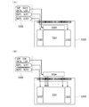
本実施の形態では、半導体装置の一態様として可視光を透過するボトムゲート型のトランジスタについて、図1(A−1)、図1(A−2)、図1(B−1)、及び図1(B−2)を用いて説明する。
(Embodiment 1)
In this embodiment, a bottom-gate transistor that transmits visible light as one embodiment of a semiconductor device is described with reference to FIGS. 1A-1, 1A-2, 1B-1, and FIG. 1 (B-2).
図1(A−1)、及び図1(A−2)は、透光性を有する導電膜を用いて、トランジスタの電極及び、当該トランジスタと接続する配線を形成する例を示す図である。 1A-1 and 1A-2 illustrate an example in which a transistor electrode and a wiring connected to the transistor are formed using a light-transmitting conductive film.
また、図1(B−1)、及び図1(B−2)は透光性を有する導電膜を用いてトランジスタの電極を形成し、金属を含む導電膜で当該トランジスタと接続する配線を形成する例を示す図である。 1B-1 and 1B-2, a transistor electrode is formed using a light-transmitting conductive film, and a wiring connected to the transistor is formed using a metal-containing conductive film. It is a figure which shows the example to do.
可視光を透過するボトムゲート型のトランジスタの構成の一態様を図1(A−1)、及び図1(A−2)に示す。図1(A−1)はトランジスタの平面構成を示す上面図であり、図1(A−2)はトランジスタの積層構成を示す断面図である。なお、図1(A−1)におけるP1−P2の鎖線は、図1(A−2)における断面P1−P2に相当する。 One mode of a structure of a bottom-gate transistor that transmits visible light is illustrated in FIGS. 1A-1 and 1A-2. 1A-1 is a top view illustrating a planar structure of a transistor, and FIG. 1A-2 is a cross-sectional view illustrating a stacked structure of the transistor. Note that a chain line P1-P2 in FIG. 1A-1 corresponds to a cross section P1-P2 in FIG.
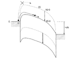
断面P1−P2は、トランジスタ151の積層構造を示している。トランジスタ151は、透光性を有する基板100上に透光性を有する第1の導電層で形成されるゲート電極111aと、ゲート電極111a上に透光性を有する第1の絶縁層102と、ゲート電極111a上の第1の絶縁層102に接してチャネル形成領域を含む透光性を有する酸化物半導体層123とを有する。
A cross section P <b> 1-P <b> 2 shows the stacked structure of the
また、ゲート電極111a上に端部を重畳し、透光性を有する第2の導電層で形成される第1の電極115aと第2の電極115bを有する。なお、第1の電極115aはバリア層114aを介して、また、第2の電極115bはバリア層114bを介して酸化物半導体層123に電気的に接続する。なお、第1の電極115aと第2の電極115bはトランジスタ151のソース電極またはドレイン電極として機能する。
In addition, the
また、トランジスタ151は、第1の電極115a、第2の電極115b、第1の絶縁層102、並びに酸化物半導体層123上に第2の絶縁層107を有する。
In addition, the
トランジスタ151を構成する全ての層は透光性を有するため、トランジスタ151は透光性を有する。
Since all the layers included in the
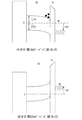
また、可視光を透過するボトムゲート型のトランジスタの構成の別の一態様を図1(B−1)、及び図1(B−2)に示す。図1(B−1)はトランジスタの平面構成を示す上面図であり、図1(B−2)はトランジスタの積層構成を示す断面図である。なお、図1(B−1)におけるQ1−Q2の鎖線は、図1(B−2)における断面Q1−Q2に相当する。 Another embodiment of the structure of the bottom-gate transistor that transmits visible light is illustrated in FIGS. 1B-1 and 1B-2. FIG. 1B-1 is a top view illustrating a planar structure of a transistor, and FIG. 1B-2 is a cross-sectional view illustrating a stacked structure of the transistor. Note that the chain line Q1-Q2 in FIG. 1B-1 corresponds to the cross section Q1-Q2 in FIG.
断面Q1−Q2は、トランジスタ152の積層構造を示している。トランジスタ152は、透光性を有する基板100上に透光性を有するゲート電極111aを有する。ゲート電極111aは図示されていない金属を含むゲート配線層と接続されている。ゲート電極111a上に透光性を有する第1の絶縁層102と、ゲート電極111a上の第1の絶縁層102に接してチャネル形成領域を含む透光性を有する酸化物半導体層123とを有する。
A cross section Q1-Q2 illustrates a stacked structure of the
また、ゲート電極111a上に端部を重畳し、透光性を有する第1の電極115aと第2の電極115bを有する。なお、第1の電極115aはバリア層114aを介して、また、第2の電極115bはバリア層114bを介して酸化物半導体層123に電気的に接続する。なお、第1の電極115aと第2の電極115bはトランジスタ152のソース電極またはドレイン電極として機能する。
In addition, the
また、第1の電極115a、第2の電極115b、酸化物半導体層123、並びに第1の絶縁層102上に第2の絶縁層107を有する。信号線116aは、第2の絶縁層107に形成した開口部127aを介して第1の電極115aと接続し、信号線116bは第2の絶縁層107に形成した開口部127bを介して第2の電極115bと接続する。
In addition, the second insulating
また、トランジスタ152は、信号線116a、信号線116b、並びに第2の絶縁層107上に第3の絶縁層108を有する。また、第3の絶縁層108上に導電層129を設けてもよい。
In addition, the
なお、第2の絶縁層107に形成した開口部126a、及び開口部126bを介して、第1の絶縁層の一部である絶縁層102aと第3の絶縁層108が互いに接する構成とする。絶縁層102aを第3の絶縁層108と同種の絶縁層とすることで、互いに密着し、トランジスタ152の周囲を囲んで接する構成となる。
Note that the insulating
なお、トランジスタ152を構成する全ての層は透光性を有するため、トランジスタ152は透光性を有する。また、トランジスタ152の電極は、金属を含む導電膜で形成した配線と接続されているため、配線抵抗が抑制された半導体装置を構成できる。また、トランジスタ152は同種の絶縁層で周囲を囲まれているため、外部からの不純物の拡散が抑制され、優れた信頼性を有する。
Note that since all the layers included in the
また、導電層129を酸化物半導体層123のチャネル形成領域と重なる位置に設けることによって、バイアス−熱ストレス試験(以下、BT試験という)におけるトランジスタ152のしきい値電圧の変化量を低減することができる。なお、BT試験に用いるストレス条件としては、85℃環境下、2×10⁶V/cm、12時間を挙げることができる。
Further, by providing the
本実施の形態では、酸化物半導体層123としてキャリア濃度が1×10¹⁴/cm3未満に抑制され、広いバンドギャップを有する高純度化されたIn−Ga−Zn−O系酸化物半導体を用いる。
In this embodiment, a highly purified In—Ga—Zn—O-based oxide semiconductor having a wide band gap and a carrier concentration of less than 1 × 10 14 / cm 3 is used as the
高純度化され、キャリア濃度が1×10¹⁴/cm3未満好ましくは1×1012/cm3以下に抑制され、広いバンドギャップ(具体的には2eV以上、好ましくは2.5eV以上、より好ましくは3eV以上)を有する酸化物半導体層をチャネル形成領域に用いたトランジスタは、ゲート電極の電位が0のときにオフ状態(所謂ノーマリーオフの特性)になる。このような酸化物半導体を用いて作製されるトランジスタは、オフ電流が小さい。 Highly purified, carrier concentration is suppressed to less than 1 × 10 14 / cm 3, preferably 1 × 10 12 / cm 3 or less, and wide band gap (specifically 2 eV or more, preferably 2.5 eV or more, more preferably A transistor in which an oxide semiconductor layer having a voltage of 3 eV or more is used for a channel formation region is turned off (so-called normally-off characteristics) when the potential of the gate electrode is 0. A transistor manufactured using such an oxide semiconductor has low off-state current.
なお、トランジスタのチャネルが形成される半導体層にキャリア濃度が1×10¹⁴/cm3未満、好ましくは1×1012/cm3以下に高純度化され、広いバンドギャップを有する酸化物半導体を適用する意義については、本実施の形態の最後に詳しく説明する。 Note that an oxide semiconductor having a wide band gap is used as the semiconductor layer in which a channel of the transistor is formed, which is highly purified to have a carrier concentration of less than 1 × 10 14 / cm 3 , preferably 1 × 10 12 / cm 3 or less. The significance of this will be described in detail at the end of the present embodiment.
酸化物半導体層としては、四元系金属酸化物であるIn−Sn−Ga−Zn−O系層や、三元系金属酸化物であるIn−Ga−Zn−O系層、In−Sn−Zn−O系層、In−Al−Zn−O系層、Sn−Ga−Zn−O系層、Al−Ga−Zn−O系層、Sn−Al−Zn−O系層や、二元系金属酸化物であるIn−Zn−O系層、Sn−Zn−O系層、Al−Zn−O系層、Zn−Mg−O系層、Sn−Mg−O系層、In−Mg−O系層や、一元系金属酸化物である、In−O系層、Sn−O系層、Zn−O系層などの酸化物半導体層を用いることができる。また、上記酸化物半導体層にSiO2を含んでもよい。 Examples of the oxide semiconductor layer include an In—Sn—Ga—Zn—O-based layer that is a quaternary metal oxide, an In—Ga—Zn—O-based layer that is a ternary metal oxide, and In—Sn—. Zn—O based layer, In—Al—Zn—O based layer, Sn—Ga—Zn—O based layer, Al—Ga—Zn—O based layer, Sn—Al—Zn—O based layer, binary system Metal oxide In—Zn—O-based layer, Sn—Zn—O-based layer, Al—Zn—O-based layer, Zn—Mg—O-based layer, Sn—Mg—O-based layer, In—Mg—O An oxide semiconductor layer such as an In—O-based layer, an Sn—O-based layer, or a Zn—O-based layer that is a single-component metal oxide can be used. Further, the oxide semiconductor layer may include SiO 2 .
InMO3(ZnO)m(m>0)のように表記される酸化物半導体材料がある。ここで、Mはガリウム(Ga)、アルミニウム(Al)、鉄(Fe)、ニッケル(Ni)、マンガン(Mn)、コバルト(Co)などから選ばれた一の金属元素または複数の金属元素を示す。例えばMとしては、Ga、Ga及びAl、Ga及びFe、Ga及びNi、Ga及びMn、Ga及びCoなどを適用することができる。MにGaを用いた、InGaO3(ZnO)m(m>0)で表記される酸化物半導体は、上記したIn―Ga―Zn―O系酸化物半導体材料の代表例である。なお、上述の組成は結晶構造から導き出されるものであり、あくまでも一例に過ぎないことを付記する。 There is an oxide semiconductor material represented as InMO 3 (ZnO) m (m> 0). Here, M represents one metal element or a plurality of metal elements selected from gallium (Ga), aluminum (Al), iron (Fe), nickel (Ni), manganese (Mn), cobalt (Co), and the like. . For example, as M, Ga, Ga and Al, Ga and Fe, Ga and Ni, Ga and Mn, Ga and Co, and the like can be applied. An oxide semiconductor represented by InGaO 3 (ZnO) m (m> 0) in which Ga is used for M is a typical example of the above-described In—Ga—Zn—O-based oxide semiconductor material. It should be noted that the above composition is derived from the crystal structure and is merely an example.
また、酸化物半導体層には、RTA(Rapid Thermal Anneal:ラピッドサーマルアニール)法等で高温短時間の脱水または脱水素化処理をしたものを用いる。酸化物半導体層は、脱水化または脱水素化の工程により酸素欠損が生じる。従って、酸素欠損部に酸素が供給される必要がある。この過程を経て高純度化された酸化物半導体層となる。高純度化された酸化物半導体層のキャリア濃度は1×10¹⁴/cm3未満、好ましくは1×1012/cm3以下に抑制される。 As the oxide semiconductor layer, a layer that has been subjected to dehydration or dehydrogenation treatment at high temperature and short time by an RTA (Rapid Thermal Annealing) method or the like is used. In the oxide semiconductor layer, oxygen vacancies are generated by the dehydration or dehydrogenation step. Therefore, oxygen needs to be supplied to the oxygen deficient part. Through this process, the oxide semiconductor layer is highly purified. The carrier concentration of the highly purified oxide semiconductor layer is suppressed to less than 1 × 10 14 / cm 3 , preferably 1 × 10 12 / cm 3 or less.
本実施の形態では、ゲート電極111aを含む第1の導電層と、第1の電極115a、及び第2の電極115bを含む第2の導電層を、透光性を有する導電膜で形成する。
In this embodiment, the first conductive layer including the
なお、透光性を有する導電膜は、可視光の透過率が75〜100%である膜厚を指す。また、可視光に対して半透明の導電膜を用いてもよい。可視光に対して半透明とは可視光の透過率が50〜75%であることを指す。 Note that a light-transmitting conductive film indicates a film thickness with a visible light transmittance of 75 to 100%. Alternatively, a conductive film that is translucent to visible light may be used. Translucent to visible light means that the visible light transmittance is 50 to 75%.
また、ゲート電極、第1の電極、及び第2の電極として用いる透光性を有する導電膜の電気抵抗率は200×10−6Ω・cm以上2000×10−6Ω・cm以下、好ましくは250×10−6Ω・cm以上2000×10−6Ω・cm以下とする。 In addition, the electrical resistivity of the light-transmitting conductive film used as the gate electrode, the first electrode, and the second electrode is 200 × 10 −6 Ω · cm to 2000 × 10 −6 Ω · cm, preferably 250 × 10 −6 Ω · cm or more and 2000 × 10 −6 Ω · cm or less.
透光性を有する導電膜としては、酸化物導電膜が好適である。具体的には、酸化タングステンを含むインジウム酸化物、酸化タングステンを含むインジウム亜鉛酸化物、酸化チタンを含むインジウム酸化物、酸化チタンを含むインジウム錫酸化物、インジウム錫酸化物(以下、ITOと示す。)、インジウム亜鉛酸化物、酸化ケイ素を添加したインジウム錫酸化物などを用いることができる。なお、酸化ケイ素を添加したインジウム錫酸化物は結晶性が抑制され、加工性に優れた非晶質な膜となる。また、酸化亜鉛、アルミニウムを添加した酸化亜鉛、ガリウムを添加した酸化亜鉛等を用いることができる。本実施の形態ではインジウム錫酸化物(ITO)を用いる。 An oxide conductive film is preferable as the light-transmitting conductive film. Specifically, indium oxide containing tungsten oxide, indium zinc oxide containing tungsten oxide, indium oxide containing titanium oxide, indium tin oxide containing titanium oxide, indium tin oxide (hereinafter referred to as ITO). ), Indium zinc oxide, indium tin oxide to which silicon oxide is added, or the like can be used. Note that indium tin oxide to which silicon oxide is added becomes an amorphous film with excellent crystallinity and excellent workability. Alternatively, zinc oxide, zinc oxide to which aluminum is added, zinc oxide to which gallium is added, or the like can be used. In this embodiment, indium tin oxide (ITO) is used.
透光性を有する酸化物導電層は、その組成、添加する不純物、並びに成膜条件により導電性を高めることができる。例えば、還元雰囲気で成膜されて酸素欠損が生じた酸化物導電層は導電性が向上する。また、不純物(例えば水素等を含む化合物等)が添加されることによって、酸化物導電層は非晶質となり加工性だけでなく、導電性も向上する。 The conductivity of the light-transmitting oxide conductive layer can be increased depending on the composition, impurities to be added, and film formation conditions. For example, the conductivity of an oxide conductive layer which is formed in a reducing atmosphere and has oxygen vacancies is improved. Further, when an impurity (for example, a compound containing hydrogen or the like) is added, the oxide conductive layer becomes amorphous, and not only the workability but also the conductivity is improved.
本実施の形態では、バリア層114a、及びバリア層114bを窒化チタンで形成する。バリア層の厚みは1nm以上50nm以下、好ましくは2nm以上10nm以下とし、透光性を有する。
In this embodiment, the
バリア層114aは、高純度化された酸化物半導体層123と第1の電極115aの間に設けられ、バリア層114bは、高純度化された酸化物半導体層123と第2の電極115bの間に設けられる。バリア層114a、及びバリア層114bは水素及び酸素の拡散を阻害する層である。
The
バリア層114a、及びバリア層114bは、酸化物導電層が含む不純物(例えば、水素原子を含む不純物)が酸化物半導体層に拡散する現象を抑制する。また、バリア層114a、及びバリア層114bは、酸化物半導体層が含む酸素原子が酸化物導電層に拡散する現象を抑制する。
The
なお、バリア層114a、及びバリア層114bとしては、窒化チタン層の他、窒化タンタル層、窒化タングステン層、窒化モリブデン層など、導電性の窒化物層や、極薄い窒化珪素層、窒化アルミニウム層など、バリア性を有する窒化物層を用いることができる。
Note that as the
本実施の形態では、第1の絶縁層102に窒化珪素(SiNy(y>0))上に、酸化珪素を積層した積層体を用いる。また、第2の絶縁層107に酸化珪素上に、窒化珪素(SiNy(y>0))を積層した積層体を用いる。
In this embodiment, a stacked body in which silicon oxide is stacked over silicon nitride (SiN y (y> 0)) as the first insulating
窒化珪素層を用いることにより、トランジスタ151に設けた酸化物半導体層123に、外部から不純物が拡散して到達する現象を防止できる。
By using the silicon nitride layer, a phenomenon in which impurities reach the
また、酸化物半導体層123と接する側の第1の絶縁層102、及び酸化物半導体層123と接する側の第2の絶縁層107に酸化珪素を用いることにより、酸化物半導体層123に生じた酸素欠損に酸素を補填できる。
In addition, when silicon oxide is used for the first insulating
なお、第1の絶縁層102、及び第2の絶縁層107を構成する酸化珪素、窒化珪素は透光性を有する。
Note that silicon oxide and silicon nitride included in the first insulating
なお、第1の絶縁層102としては、窒化酸化珪素層、酸化窒化珪素層、窒化珪素層または酸化珪素層の他、アルミニウム、タンタル、イットリウム、またはハフニウムの酸化物、窒化物、酸化窒化物、又は窒化酸化物の一種又はそれらの化合物を少なくとも2種以上含む化合物層を単層で、または積層して用いることもできる。
Note that as the first insulating
特に、第1の絶縁層102に酸化珪素より高い誘電率を有する絶縁層を用いると、ゲート絶縁層としての特性が向上するため好ましい。
In particular, an insulating layer having a dielectric constant higher than that of silicon oxide is preferably used for the first insulating
また、基板100は可視光を透過し、絶縁表面を有するものを用いる。例えば、ガラス基板、セラミック基板の他、作製工程の処理温度に耐えうる程度の耐熱性を有するプラスチック基板等を用いることができる。
The
ガラス基板としては、例えば、バリウムホウケイ酸ガラス、アルミノホウケイ酸ガラス若しくはアルミノケイ酸ガラス等の無アルカリガラス基板を用いるとよい。他に、石英基板、サファイア基板などを用いることができる。本実施の形態では、基板100にアルミノホウケイ酸ガラスを用いる。
As the glass substrate, for example, an alkali-free glass substrate such as barium borosilicate glass, aluminoborosilicate glass, or aluminosilicate glass may be used. In addition, a quartz substrate, a sapphire substrate, or the like can be used. In this embodiment mode, aluminoborosilicate glass is used for the
また、基板の大きさは、使用目的、製造装置等を勘案して、適宜決定すればよいが、第3世代(550mm×650mm)、第3.5世代(600mm×720mm、または620mm×750mm)、第4世代(680mm×880mm、または730mm×920mm)、第5世代(1100mm×1300mm)、第6世代(1500mm×1850mm)、第7世代(1870mm×2200mm)、第8世代(2200mm×2400mm)、第9世代(2400mm×2800mm、2450mm×3050mm)、第10世代(2950mm×3400mm)等のガラス基板を用いることができる。 The size of the substrate may be appropriately determined in consideration of the purpose of use, the manufacturing apparatus, etc., but the third generation (550 mm × 650 mm), the third generation (600 mm × 720 mm, or 620 mm × 750 mm). , 4th generation (680mm x 880mm, or 730mm x 920mm), 5th generation (1100mm x 1300mm), 6th generation (1500mm x 1850mm), 7th generation (1870mm x 2200mm), 8th generation (2200mm x 2400mm) , Glass substrates of the ninth generation (2400 mm × 2800 mm, 2450 mm × 3050 mm), the tenth generation (2950 mm × 3400 mm) and the like can be used.
なお基板100上に、下地膜として、窒化珪素膜、窒化酸化珪素膜を、単層若しくは積層して形成することができる。下地膜は、スパッタリング法、CVD法、塗布法、印刷法等を適宜用いることができる。なお、膜中にリン(P)や硼素(B)がドープされていても良い。
Note that a silicon nitride film or a silicon nitride oxide film can be formed as a single layer or stacked over the
ここでは、トランジスタのチャネルが形成される半導体層にキャリア濃度が1×10¹⁴/cm3未満、好ましくは1×1012/cm3以下に高純度化され、広いバンドギャップを有する酸化物半導体を適用する意義について説明する。 Here, an oxide semiconductor having a wide band gap is formed in a semiconductor layer in which a channel of a transistor is formed with a high carrier concentration of less than 1 × 10 14 / cm 3 , preferably 1 × 10 12 / cm 3 or less. The significance of application will be explained.
<酸化物半導体の真性化>
酸化物半導体において、DOS(density of state)等の物性研究は多くなされているが、これらの研究は、局在準位そのものを十分に減らすという思想を含まない。開示する発明の一態様では、局在準位の原因たり得る水や水素を酸化物半導体中より除去することで、高純度化し、真性化(i型化)した酸化物半導体を作製する。これは、局在準位そのものを十分に減らすという思想に立脚するものである。そして、これによって極めて優れた工業製品の製造を可能とするものである。
<Intrinsic oxide semiconductors>
Many studies on physical properties of oxide semiconductors such as DOS (Density of State) have been made, but these studies do not include the idea of sufficiently reducing the localized level itself. In one embodiment of the disclosed invention, highly purified and intrinsic (i-type) oxide semiconductor is manufactured by removing water and hydrogen that may cause localized states from an oxide semiconductor. This is based on the idea of sufficiently reducing the localized level itself. This makes it possible to produce extremely excellent industrial products.
なお、水素や水などを除去する際には、同時に酸素が除去されてしまうことがある。このため、酸素欠乏により発生する金属の未結合手に対して酸素を供給し、酸素欠陥による局在準位を減少させることにより、酸化物半導体をさらに高純度化、真性化(i型化)するのは好適である。たとえば、酸化物半導体を含むチャネル形成領域に密接して酸素過剰の酸化膜を形成し、200℃〜400℃、代表的には250℃程度の温度条件での熱処理を行うことで、当該酸化膜から酸化物半導体へ酸素を供給して、酸素欠陥による局在準位を低減させることが可能である。 When removing hydrogen or water, oxygen may be removed at the same time. For this reason, oxygen is supplied to the dangling bonds of the metal generated by oxygen deficiency, and the localized states due to oxygen defects are reduced, whereby the oxide semiconductor is further purified and made intrinsic (i-type). It is suitable to do. For example, an oxide film containing excess oxygen is formed in close contact with a channel formation region containing an oxide semiconductor, and heat treatment is performed at a temperature of about 200 ° C. to 400 ° C., typically about 250 ° C. Oxygen can be supplied from the oxide semiconductor to the oxide semiconductor to reduce localized levels due to oxygen defects.
酸化物半導体の特性を悪化させる要因は、過剰な水素による伝導帯下0.1eV〜0.2eVの浅い準位や、酸素欠損による深い準位、などに起因するものと考えられる。これらの欠陥をなくすために、水素を徹底的に除去し、酸素を十分に供給する。 A factor that deteriorates the characteristics of an oxide semiconductor is considered to be due to a shallow level of 0.1 eV to 0.2 eV below a conduction band due to excess hydrogen, a deep level due to oxygen deficiency, or the like. In order to eliminate these defects, hydrogen is thoroughly removed and oxygen is sufficiently supplied.
なお、酸化物半導体は一般にn型とされているが、開示する発明の一態様では、水や水素などの不純物を除去すると共に、酸化物半導体の構成元素である酸素を供給することでi型化を実現する。この点、シリコンなどのように不純物元素を添加してのi型化ではなく、従来にない技術思想を含むものといえる。 Note that an oxide semiconductor is generally n-type; however, in one embodiment of the disclosed invention, an impurity such as water or hydrogen is removed and oxygen that is a constituent element of the oxide semiconductor is supplied to increase i-type. Realize. In this respect, it can be said that it includes an unprecedented technical idea rather than i-type by adding an impurity element such as silicon.
<酸化物半導体を用いたトランジスタの電導機構>
ここで、酸化物半導体を用いたトランジスタの電導機構につき、図2乃至図5を用いて説明する。なお、以下の説明では、理解の容易のため理想的な状況を仮定しており、そのすべてが現実の様子を反映しているとは限らない。また、以下の説明はあくまでも一考察に過ぎず、発明の有効性に影響を与えるものではないことを付記する。
<Conductive mechanism of transistor using oxide semiconductor>
Here, a conduction mechanism of a transistor including an oxide semiconductor will be described with reference to FIGS. In the following description, an ideal situation is assumed for easy understanding, and not all of them reflect the actual situation. In addition, it is noted that the following description is merely a consideration and does not affect the effectiveness of the invention.
図2は、酸化物半導体を用いたトランジスタの断面図である。ゲート電極(GE1)上にゲート絶縁層(GI)を介して酸化物半導体層(OS)が設けられ、その上にソース電極(S)及びドレイン電極(D)が設けられている。 FIG. 2 is a cross-sectional view of a transistor including an oxide semiconductor. An oxide semiconductor layer (OS) is provided over the gate electrode (GE1) through a gate insulating layer (GI), and a source electrode (S) and a drain electrode (D) are provided thereover.
図3には、図2のA−A’断面におけるエネルギーバンド図(模式図)を示す。また、図3中の黒丸(●)は電子を示し、白丸(○)は正孔を示し、それぞれは電荷(−q,+q)を有している。ドレイン電極に正の電圧(VD>0)を印加した上で、破線はゲート電極に電圧を印加しない場合(VG=0)、実線はゲート電極に正の電圧(VG>0)を印加する場合を示す。ゲート電極に電圧を印加しない場合は高いポテンシャル障壁のために電極から酸化物半導体側へキャリア(電子)が注入されず、電流を流さないオフ状態を示す。一方、ゲートに正の電圧を印加するとポテンシャル障壁が低下し、電流を流すオン状態を示す。 FIG. 3 shows an energy band diagram (schematic diagram) in the AA ′ cross section of FIG. In FIG. 3, black circles (●) indicate electrons, white circles (◯) indicate holes, and each has a charge (−q, + q). When a positive voltage (V D > 0) is applied to the drain electrode and no voltage is applied to the gate electrode (V G = 0), a broken line indicates a positive voltage (V G > 0) to the gate electrode. The case of applying is shown. When no voltage is applied to the gate electrode, carriers (electrons) are not injected from the electrode to the oxide semiconductor side due to a high potential barrier, and an off state in which no current flows is shown. On the other hand, when a positive voltage is applied to the gate, the potential barrier is lowered, indicating an on state in which current flows.
図4には、図2におけるB−B’の間におけるエネルギーバンド図(模式図)を示す。図4(A)は、ゲート電極(GE1)に正の電位(VG>0)が与えられた状態であり、ソースとドレインとの間にキャリア(電子)が流れるオン状態を示している。また、図4(B)は、ゲート(GE1)に負の電位(VG<0)が印加された状態であり、オフ状態(少数キャリアは流れない状態)である場合を示す。 FIG. 4 shows an energy band diagram (schematic diagram) between BB ′ in FIG. FIG. 4A shows a state in which a positive potential (V G > 0) is applied to the gate electrode (GE1), and shows an on state in which carriers (electrons) flow between the source and the drain. FIG. 4B illustrates a case where a negative potential (V G <0) is applied to the gate (GE1) and an off state (a state where minority carriers do not flow).
図5は、真空準位と金属の仕事関数(φM)、酸化物半導体の電子親和力(χ)の関係を示す。 FIG. 5 shows the relationship between the vacuum level, the metal work function (φ M ), and the electron affinity (χ) of the oxide semiconductor.
常温において金属中の電子は縮退しており、フェルミ準位は伝導帯内に位置する。従来の酸化物半導体はn型であり、そのフェルミ準位(Ef)は、バンドギャップ中央に位置する真性フェルミ準位(Ei)から離れて、伝導帯寄りに位置している。なお、酸化物半導体において水素はドナーとなりn型化する要因の一つであることが知られている。 At room temperature, the electrons in the metal are degenerated and the Fermi level is located in the conduction band. A conventional oxide semiconductor is n-type, and its Fermi level (E f ) is located closer to the conduction band, away from the intrinsic Fermi level (E i ) located in the center of the band gap. Note that it is known that hydrogen in an oxide semiconductor is a factor that becomes a donor and becomes n-type.
これに対して開示する発明の一態様に係る酸化物半導体は、n型化の要因である水素を酸化物半導体から除去し、酸化物半導体の主成分以外の元素(不純物元素)が極力含まれないように高純度化することにより真性(i型)とし、または真性とせんとしたものである。すなわち、不純物元素を添加してi型化するのでなく、水素や水等の不純物を極力除去することにより、高純度化された結果、真性(i型)またはそれに近づけることを特徴としている。これにより、フェルミ準位(Ef)は真性フェルミ準位(Ei)と同程度とすることができる。 In contrast, an oxide semiconductor according to one embodiment of the disclosed invention removes hydrogen which is a factor of n-type conversion from an oxide semiconductor and includes an element (impurity element) other than the main component of the oxide semiconductor as much as possible. It is made intrinsic (i-type) by purifying it so that it does not exist, or it is made genuine. That is, it is characterized in that it is made intrinsic (i-type) or close to it as a result of being highly purified by removing impurities such as hydrogen and water as much as possible instead of adding an impurity element to i-type. Accordingly, the Fermi level (E f ) can be set to the same level as the intrinsic Fermi level (E i ).
酸化物半導体のバンドギャップ(Eg)は3.15eVで、電子親和力(χ)は4.3Vと言われている。ソース電極及びドレイン電極を構成するチタン(Ti)の仕事関数は、酸化物半導体の電子親和力(χ)とほぼ等しい。この場合、金属−酸化物半導体界面において、電子に対してショットキー型の障壁は形成されない。 An oxide semiconductor has a band gap (E g ) of 3.15 eV and an electron affinity (χ) of 4.3 V. The work function of titanium (Ti) constituting the source electrode and the drain electrode is substantially equal to the electron affinity (χ) of the oxide semiconductor. In this case, no Schottky barrier is formed for electrons at the metal-oxide semiconductor interface.
このとき電子は、図4(A)で示すように、ゲート絶縁層と高純度化された酸化物半導体との界面付近(酸化物半導体のエネルギー的に安定な最低部)を移動する。 At this time, as shown in FIG. 4A, electrons move in the vicinity of the interface between the gate insulating layer and the highly purified oxide semiconductor (the lowest energy-stable minimum portion of the oxide semiconductor).
また、図4(B)に示すように、ゲート電極(GE1)に負の電位が与えられると、少数キャリアであるホールは実質的にゼロであるため、電流は限りなくゼロに近い値となる。 In addition, as shown in FIG. 4B, when a negative potential is applied to the gate electrode (GE1), the number of holes that are minority carriers is substantially zero, and thus the current becomes a value close to zero. .
このように酸化物半導体の主成分以外の元素(不純物元素)が極力含まれないように高純度化することにより、真性(i型)とし、または実質的に真性となるため、ゲート絶縁層との界面特性が顕在化する。そのため、ゲート絶縁層には、酸化物半導体と良好な界面を形成できるものが要求される。具体的には、例えば、VHF帯〜マイクロ波帯の電源周波数で生成される高密度プラズマを用いたCVD法で作製される絶縁層や、スパッタリング法で作製される絶縁層などを用いることが好ましい。 In this manner, by being highly purified so that an element other than the main component of the oxide semiconductor (impurity element) is not included as much as possible, it becomes intrinsic (i-type) or substantially intrinsic. The interface characteristics of Therefore, a gate insulating layer that can form a favorable interface with an oxide semiconductor is required. Specifically, for example, an insulating layer manufactured by a CVD method using high-density plasma generated at a power supply frequency in the VHF band to a microwave band, an insulating layer manufactured by a sputtering method, or the like is preferably used. .
酸化物半導体を高純度化しつつ、酸化物半導体とゲート絶縁層との界面を良好なものとすることにより、例えば、トランジスタのチャネル幅Wが1×104μm、チャネル長Lが3μmの場合には、常温で、10−13A以下のオフ電流、0.1V/dec.のサブスレッショルドスイング値(S値)(ゲート絶縁層の厚さ:100nm)が実現され得る。 For example, when the transistor has a channel width W of 1 × 10 4 μm and a channel length L of 3 μm by improving the purity of the oxide semiconductor and improving the interface between the oxide semiconductor and the gate insulating layer. Is an off current of 10 −13 A or less at room temperature, 0.1 V / dec. The subthreshold swing value (S value) (gate insulating layer thickness: 100 nm) can be realized.
このように、酸化物半導体の主成分以外の元素(不純物元素)が極力含まれないように高純度化することにより、トランジスタの動作を良好なものとすることができる。 As described above, the operation of the transistor can be improved by increasing the purity so that an element (impurity element) other than the main component of the oxide semiconductor is not included as much as possible.
このように透光性を有する材料で構成する本実施の形態のトランジスタは透光性を有する。 As described above, the transistor of this embodiment including a light-transmitting material has a light-transmitting property.
本実施の形態のトランジスタは、酸素欠損や不純物(例えば水素等)を含み、導電率が高められた酸化物導電層を用いてソース電極、及びドレイン電極を形成しているため、オン電流の損失が少ない。 In the transistor of this embodiment, the source electrode and the drain electrode are formed using an oxide conductive layer containing oxygen deficiency and impurities (for example, hydrogen) and having increased conductivity. Less is.
広いバンドギャップを有し、キャリア濃度を1×10¹⁴/cm3未満、好ましくは1×1012/cm3以下に抑制された酸化物半導体を用いるため、本実施の形態のトランジスタはノーマリーオフの挙動を示し、そのオフ電流は低い。具体的には、チャネル幅1μmあたりの室温でのオフ電流を1×10−16A/μm以下、さらには1aA/μm(1×10−18A/μm)以下にすることが可能である。 Since an oxide semiconductor having a wide band gap and a carrier concentration suppressed to less than 1 × 10 14 / cm 3 , preferably 1 × 10 12 / cm 3 or less is used, the transistor in this embodiment is normally off. The off-state current is low. Specifically, the off current at room temperature per channel width of 1 μm can be set to 1 × 10 −16 A / μm or less, further 1 aA / μm (1 × 10 −18 A / μm) or less.
なお、トランジスタのオフ電流の流れ難さをオフ抵抗率として表すことができる。オフ抵抗率とは、トランジスタがオフのときのチャネル形成領域の抵抗率であり、オフ抵抗率はオフ電流から算出することができる。 Note that the difficulty of off-state current flow in a transistor can be expressed as off-resistance. The off resistivity is the resistivity of the channel formation region when the transistor is off, and the off resistivity can be calculated from the off current.
具体的には、オフ電流とドレイン電圧との値が分かればオームの法則からトランジスタがオフのときの抵抗値(オフ抵抗R)を算出することができる。そして、チャネル形成領域の断面積Aとチャネル形成領域の長さ(ソースドレイン電極間の距離に相当する)Lが分かればρ=RA/Lの式(Rはオフ抵抗)からオフ抵抗率ρを算出することができる。 Specifically, if the values of the off current and the drain voltage are known, the resistance value (off resistance R) when the transistor is off can be calculated from Ohm's law. If the cross-sectional area A of the channel formation region and the length L of the channel formation region (corresponding to the distance between the source and drain electrodes) L are known, the off resistivity ρ can be calculated from the equation ρ = RA / L (R is the off resistance). Can be calculated.
ここで、断面積Aは、チャネル形成領域の膜厚をdとし、チャネル幅をWとするとき、A=dWから算出することができる。また、チャネル形成領域の長さLはチャネル長Lである。以上のように、オフ電流からオフ抵抗率を算出することができる。 Here, the cross-sectional area A can be calculated from A = dW where d is the thickness of the channel formation region and W is the channel width. The length L of the channel formation region is the channel length L. As described above, the off resistivity can be calculated from the off current.
本実施の形態の酸化物半導体層を具備するトランジスタのオフ抵抗率は1×10⁹Ω・m以上の優れた値を示す。 The off-resistivity of the transistor including the oxide semiconductor layer of this embodiment has an excellent value of 1 × 10 9 Ω · m or more.
本実施の形態のトランジスタにおいて、酸化物導電層と高純度化された酸化物半導体層の間に水素及び酸素の拡散を阻害するバリア層を設けているため、酸化物導電層が含む不純物(例えば、水素原子を含む不純物)が酸化物半導体層に拡散する現象が抑制される。また、バリア層によって、酸化物半導体層が含む酸素原子が酸化物導電層に拡散する現象が抑制される。 In the transistor of this embodiment, since a barrier layer that inhibits diffusion of hydrogen and oxygen is provided between the oxide conductive layer and the highly purified oxide semiconductor layer, impurities contained in the oxide conductive layer (for example, , Impurities including hydrogen atoms) are prevented from diffusing into the oxide semiconductor layer. In addition, the barrier layer suppresses a phenomenon in which oxygen atoms included in the oxide semiconductor layer are diffused into the oxide conductive layer.
本実施の形態で例示した透光性を有するトランジスタは、高純度化された酸化物半導体層がバリア層により保護されているため、ノーマリーオフの特性と、オフ電流が低減された特性を有し、また経時的に特性が変化し難く、信頼性に優れている。 The light-transmitting transistor illustrated in this embodiment has normally-off characteristics and reduced off-state current because the highly purified oxide semiconductor layer is protected by a barrier layer. In addition, the characteristics hardly change over time, and the reliability is excellent.
なお、本実施の形態は、本明細書で示す他の実施の形態と適宜組み合わせることができる。 Note that this embodiment can be combined with any of the other embodiments described in this specification as appropriate.
(実施の形態2)
本実施の形態では、半導体装置の一態様として可視光を透過するボトムゲート型のトランジスタを適用した表示装置について図6を用いて説明する。また、可視光を透過するボトムゲート型のトランジスタの作製方法について、図7を用いて説明する。
(Embodiment 2)
In this embodiment, a display device using a bottom-gate transistor that transmits visible light as one embodiment of a semiconductor device will be described with reference to FIGS. A method for manufacturing a bottom-gate transistor that transmits visible light is described with reference to FIGS.
なお、可視光を透過するボトムゲート型のトランジスタと共に作製可能なチャネル保護型のトランジスタの作製方法についても、図7を用いて説明する。 Note that a method for manufacturing a channel-protective transistor that can be manufactured with a bottom-gate transistor that transmits visible light is also described with reference to FIGS.
図6(A)は、可視光を透過するボトムゲート型のトランジスタを適用した表示装置の画素部の上面図である。また、図6(B)は、可視光を透過するボトムゲート型のトランジスタを適用した表示装置の画素部の積層構成を示す断面図である。なお、図6(A)におけるA1−A2の鎖線は、図6(B)における断面A1−A2に相当し、図6(A)におけるB1−B2の鎖線は、図6(B)における断面B1−B2に相当し、図6(A)におけるC1−C2の鎖線は、図6(B)における断面C1−C2に相当し、図6(A)におけるD1−D2の鎖線は、図6(B)における断面D1−D2に相当する。 FIG. 6A is a top view of a pixel portion of a display device to which a bottom-gate transistor that transmits visible light is applied. FIG. 6B is a cross-sectional view illustrating a stacked structure of a pixel portion of a display device to which a bottom-gate transistor that transmits visible light is applied. Note that the chain line A1-A2 in FIG. 6A corresponds to the cross section A1-A2 in FIG. 6B, and the chain line B1-B2 in FIG. 6A is the cross section B1 in FIG. 6B corresponds to the cross section C1-C2 in FIG. 6B, and the D1-D2 chain line in FIG. 6A corresponds to FIG. Corresponds to the cross section D1-D2 in FIG.
断面A1−A2はトランジスタ153の積層構造を説明する図である。また、断面D1−D2はトランジスタ153の積層構造を断面A1−A2とは異なる断面から説明する図である。
A cross section A1-A2 illustrates a stacked structure of the
トランジスタ153は、透光性を有する基板100上にゲート電極111aを有する。なお、ゲート電極111aはゲート配線111cと電気的に接続されている。また、ゲート電極111a上に第1の絶縁層102を有し、ゲート電極111a上の第1の絶縁層102に接して酸化物半導体層123を有する。また、ゲート電極111a上に端部を重畳する第1の電極115a、及び第2の電極115bを有する。なお、第1の電極115aと酸化物半導体層123の間にはバリア層114aを有し、第2の電極115bと酸化物半導体層123の間にはバリア層114bを有する。
The
ゲート電極111a上で、酸化物半導体層123と第1の電極115aとが重なる領域と、酸化物半導体層123と第2の電極115bとが重なる領域の間で、第2の絶縁層107と酸化物半導体層123は接する。第2の絶縁層107に開口部127を形成し、信号線116aを設け、第2の絶縁層107及び信号線116a上に第3の絶縁層108を有し、第3の絶縁層108上に第4の絶縁層109を有する。また、第2の絶縁層107、第3の絶縁層108、及び第4の絶縁層109に形成した開口部128を介して第2の電極115bと電気的に接続する画素電極120を第4の絶縁層109上に有する。
On the
断面B1−B2は容量部の積層構造を説明する図である。 Cross-section B1-B2 is a diagram for explaining the laminated structure of the capacitor portion.
容量部は基板100上に設けられた第1の容量電極111b上に、第1の絶縁層102及びバリア層114bを挟んでトランジスタ153の第2の電極115bが延在して形成されている。第1の容量電極111bは、トランジスタ153のゲート電極111aと共に形成し、第1の絶縁層102、バリア層114b、並びに第2の電極115bはトランジスタ153と共に作製できる。
The capacitor portion is formed on the
第1の容量電極111b及び第2の電極115bは透光性を有するため、容量部は透光性を有し、画素の開口率が低下しない。また、第1の容量電極111b及び第2の電極115bの間隔が狭いため、大きな容量が得られる。
Since the
断面C1−C2はゲート配線111cと信号線116aの交差部の断面構造を説明する図である。
A cross section C1-C2 is a diagram illustrating a cross-sectional structure of an intersection of the
基板100上に設けられたゲート配線111c上に第1の絶縁層102、酸化物半導体層113c、第2の絶縁層107を挟んで信号線116aが交差する。ゲート配線111cはトランジスタ153のゲート電極と接続する。
The
ゲート配線111cと信号線116aの交差部において、その間隔が広げられているため、配線容量が低減されている。
Since the interval between the
次に、可視光を透過するボトムゲート型のトランジスタ153の作製方法について図7を用いて説明する。
Next, a method for manufacturing the
図7(D)に示すトランジスタ153は、図6に示す表示装置の画素部に適用された可視光を透過するボトムゲート型のトランジスタと同じ構成を有する。
A
なお、図7(D)には、トランジスタ153と異なる構成を有するが、トランジスタ153と並行して同一基板上に作製可能なトランジスタ154も例示されている。
Note that FIG. 7D also illustrates a
トランジスタ154は、ゲート配線111cと同一の材料からなるゲート電極111dを有し、信号線116aと同一の材料で形成された第3の電極116c、及び第4の電極116dを有する。また、トランジスタ154は、酸化物半導体層113cのチャネル形成領域上に絶縁層107cを有し、絶縁層107cはチャネル保護層として機能する。
The
なお、本実施の形態において、「Aと同一の材料からなるB」とは、AとBが同一の工程にて同一の材料から形成されることを指す。 In the present embodiment, “B made of the same material as A” means that A and B are made of the same material in the same step.
本実施の形態では、基板100にアルミノホウケイ酸ガラスを用いる。
In this embodiment mode, aluminoborosilicate glass is used for the
はじめに、ゲート電極111a、ゲート電極111d、並びにゲート電極と電気的に接続するゲート配線を形成する。本実施の形態では、ゲート電極111aとなる導電層とゲート配線を含む導電層を合わせて第1の導電層と呼ぶ。なお、ゲート配線は図7には図示されていない。
First, the
本実施の形態では、ゲート配線及びゲート電極111dをチタン層とアルミニウム層とチタン層を積層した3層構造の導電層を用い、可視光を透過するゲート電極111aとなる導電層にインジウム錫酸化物(ITO)を用いる。
In this embodiment, the gate wiring and the
基板100上に、スパッタリング法を用いて、チタン層とアルミニウム層とチタン層を積層した3層構造の導電層を成膜する。次いで、第1のフォトリソグラフィ工程で形成したレジストマスクを用いて選択的にエッチングしてゲート電極111d、及びゲート配線を形成する。なお、ゲート配線と同一の材料で形成するゲート電極111dは、トランジスタ154のゲート電極となる。
A conductive layer having a three-layer structure in which a titanium layer, an aluminum layer, and a titanium layer are stacked is formed over the
次に、インジウム錫酸化物(ITO)を成膜し、第2のフォトリソグラフィ工程で形成したレジストマスクを用いて選択的にエッチングし、透光性を有するゲート電極111aを形成する。なお、透光性を有するゲート電極111aはトランジスタ153のゲート電極となる。
Next, indium tin oxide (ITO) is formed and selectively etched using the resist mask formed in the second photolithography step, so that the light-transmitting
ゲート配線を形成する導電膜としては、Al、Cu、Cr、Ta、Ti、Mo、Wなどの金属材料、または該金属材料を成分とする合金材料で形成する。また、Al、Cuなどの金属膜の一方または双方にCr、Ta、Ti、Mo、Wなどの高融点金属膜を積層させた構成としても良い。また、Si、Ti、Ta、W、Mo、Cr、Nd、Sc、YなどAl膜に生ずるヒロックやウィスカーの発生を防止する元素が添加されているAl材料を用いることで耐熱性を向上させることが可能となる。 The conductive film for forming the gate wiring is formed using a metal material such as Al, Cu, Cr, Ta, Ti, Mo, or W, or an alloy material containing the metal material as a component. Alternatively, a configuration may be adopted in which a refractory metal film such as Cr, Ta, Ti, Mo, or W is laminated on one or both of metal films such as Al and Cu. Moreover, heat resistance is improved by using an Al material to which an element for preventing generation of hillocks and whiskers generated in an Al film such as Si, Ti, Ta, W, Mo, Cr, Nd, Sc, and Y is added. Is possible.
本実施の形態では、ゲート配線を形成した後に透光性を有するゲート電極を形成する場合について説明したが、透光性を有するゲート電極を形成した後にゲート配線を形成してもよい。 In this embodiment, the case where the light-transmitting gate electrode is formed after the gate wiring is formed is described; however, the gate wiring may be formed after the light-transmitting gate electrode is formed.
次に、第1の絶縁層102を形成する。本実施の形態では、窒化珪素層上に酸化珪素を積層して第1の絶縁層102を形成する。
Next, the first insulating
第1の絶縁層102は酸化珪素層、酸化窒化珪素層、窒化酸化珪素層、窒化珪素層、酸化アルミニウム層、酸化タンタル層などの単層膜または積層膜を用いることができる。また、膜厚を50nm以上250nm以下とし、CVD法やスパッタ法などで形成する。また、膜中にリン(P)や硼素(B)がドープされていても良い。
The first insulating
なお、第1の絶縁層102は酸化物半導体層と接する側に酸化物絶縁層を有する構成が好ましい。また、本実施の形態で用いる、不純物を除去することによりi型化または実質的にi型化された酸化物半導体(高純度化された酸化物半導体)は界面準位、界面電荷に対して極めて敏感であるため、絶縁層との界面は重要である。そのため高純度化された酸化物半導体に接する絶縁層は、高品質化が要求される。
Note that the first insulating
次いで、酸化物半導体層を形成する。本実施の形態では、In−Ga−Zn−O系酸化物半導体成膜用ターゲットをスパッタリングして成膜したIn−Ga−Zn−O系非単結晶膜から、酸化物半導体層を形成する。 Next, an oxide semiconductor layer is formed. In this embodiment, an oxide semiconductor layer is formed from an In—Ga—Zn—O-based non-single-crystal film formed by sputtering an In—Ga—Zn—O-based oxide semiconductor deposition target.
酸化物半導体層の膜厚は5nm以上200nm以下、好ましくは10nm以上20nm以下、例えば15nmとする。 The thickness of the oxide semiconductor layer is 5 nm to 200 nm, preferably 10 nm to 20 nm, for example, 15 nm.
なお、酸化物半導体層を成膜する前に、アルゴンガスを導入してプラズマを発生させる逆スパッタを行い、第1の絶縁層102の表面に付着しているゴミを除去することが好ましい。
Note that before the oxide semiconductor layer is formed, dust attached to the surface of the first insulating
逆スパッタとは、アルゴン雰囲気下で基板にRF電源を用いて電圧を印加してプラズマを形成して表面を改質する方法である。なお、アルゴン雰囲気に代えて窒素、ヘリウムなどを用いてもよい。また、アルゴン雰囲気に酸素、N2Oなどを加えた雰囲気で行ってもよい。また、アルゴン雰囲気にCl2、CF4などを加えた雰囲気で行ってもよい。 Reverse sputtering is a method for modifying the surface by forming a plasma by applying a voltage to the substrate using an RF power source in an argon atmosphere. Note that nitrogen, helium, or the like may be used instead of the argon atmosphere. Alternatively, an argon atmosphere may be used in which oxygen, N 2 O, or the like is added. Alternatively, an atmosphere obtained by adding Cl 2 , CF 4, or the like to an argon atmosphere may be used.
また、逆スパッタ処理後、大気に曝すことなく酸化物半導体膜を成膜することによって、第1の絶縁層102と酸化物半導体層の界面にゴミや水分が付着するのを防ぐことができる。
Further, after the reverse sputtering treatment, the oxide semiconductor film is formed without being exposed to the air, whereby dust and moisture can be prevented from attaching to the interface between the first insulating
また、酸化物半導体膜は、希ガス(代表的にはアルゴン)雰囲気下、酸素雰囲気下、又は希ガス(代表的にはアルゴン)及び酸素混合雰囲気下においてスパッタ法により形成することができる。また、スパッタ法を用いる場合、SiO2を2重量%以上10重量%以下含むターゲットを用いて成膜を行い、酸化物半導体膜に結晶化を阻害するSiOx(X>0)を含ませても良い。 The oxide semiconductor film can be formed by a sputtering method in a rare gas (typically argon) atmosphere, an oxygen atmosphere, or a rare gas (typically argon) and oxygen mixed atmosphere. Further, in the case of using a sputtering method, film formation is performed using a target containing SiO 2 in an amount of 2 wt% to 10 wt%, and SiO x (X> 0) that inhibits crystallization is included in the oxide semiconductor film. good.
ここでは、In、Ga、及びZnを含む酸化物半導体成膜用ターゲット(モル数比がIn2O3:Ga2O3:ZnO=1:1:1[mol数比]、またはIn2O3:Ga2O3:ZnO=1:1:2[mol数比])を用いて、基板とターゲットの間との距離を100mm、圧力0.6Pa、直流(DC)電源0.5kW、酸素(酸素流量比率100%)雰囲気下で成膜する。なお、パルス直流(DC)電源を用いると、ごみが軽減でき、膜厚分布も均一となるために好ましい。
Here, a target for forming an oxide semiconductor film containing In, Ga, and Zn (molar ratio is In 2 O 3 : Ga 2 O 3 : ZnO = 1: 1: 1 [molar ratio], or In 2 O 3 : Ga 2 O 3 : ZnO = 1: 1: 2 [molar ratio]), the distance between the substrate and the target is 100 mm, the pressure is 0.6 Pa, the direct current (DC) power supply is 0.5 kW, oxygen The film is formed under an atmosphere (
この場合において、処理室内の残留水分を除去しつつ酸化物半導体膜を成膜することが好ましい。酸化物半導体膜に水素、水酸基又は水分が含まれないようにするためである。 In this case, it is preferable to form the oxide semiconductor film while removing residual moisture in the treatment chamber. This is for preventing hydrogen, a hydroxyl group, and moisture from being contained in the oxide semiconductor film.
本実施の形態で用いるマルチチャンバー型のスパッタリング装置は、珪素もしくは酸化珪素(人工石英)ターゲットと、酸化物半導体成膜用のターゲットを備えており、少なくとも、酸化物半導体成膜用のターゲットを設けた成膜室は、排気手段としてクライオポンプを有している。なお、クライオポンプに代えて、ターボ分子ポンプを用い、当該ターボ分子ポンプの吸気口上に水分などを吸着させるべくコールドトラップを設ける構成としても良い。 The multi-chamber sputtering apparatus used in this embodiment includes a silicon or silicon oxide (artificial quartz) target and an oxide semiconductor film formation target, and at least the oxide semiconductor film formation target is provided. The film formation chamber has a cryopump as an exhaust means. Instead of the cryopump, a turbo molecular pump may be used, and a cold trap may be provided on the intake port of the turbo molecular pump to adsorb moisture or the like.
クライオポンプを用いて排気した成膜室は、例えば、水素原子や、H2Oなど水素原子を含む化合物や、炭素原子や炭素原子を含む化合物等が排気されるため、当該成膜室で成膜した酸化物半導体膜に含まれる不純物の濃度を低減できる。 A film formation chamber evacuated using a cryopump is formed in the film formation chamber because, for example, hydrogen atoms, compounds containing hydrogen atoms such as H 2 O, and compounds containing carbon atoms or carbon atoms are exhausted. The concentration of impurities contained in the formed oxide semiconductor film can be reduced.
なお、酸化物半導体膜を第1の絶縁層102上に連続成膜するのが好ましい。
Note that an oxide semiconductor film is preferably formed continuously over the first insulating
酸化物半導体膜を、成膜する際に用いるスパッタガスは水素、水、水酸基又は水素化物などの不純物が、濃度1ppm程度、濃度10ppb程度まで除去された高純度ガスを用いることが好ましい。 As a sputtering gas used for forming the oxide semiconductor film, a high-purity gas from which impurities such as hydrogen, water, a hydroxyl group, or hydride are removed to a concentration of about 1 ppm and a concentration of about 10 ppb is preferably used.
また、酸化物半導体膜は基板を加熱しながら成膜してもよい。このとき基板温度を100℃以上600℃以下好ましくは200℃以上400℃以下とする。基板を加熱しながら成膜することにより、成膜した酸化物半導体膜に含まれる不純物濃度を低減することができる。 The oxide semiconductor film may be formed while the substrate is heated. At this time, the substrate temperature is set to 100 ° C. or higher and 600 ° C. or lower, preferably 200 ° C. or higher and 400 ° C. or lower. By forming the film while heating the substrate, the concentration of impurities contained in the formed oxide semiconductor film can be reduced.
次に、第3のフォトリソグラフィ工程で形成したレジストマスクを用いて選択的にエッチングし、In−Ga−Zn−O系非単結晶からなる島状の酸化物半導体層113a、及び酸化物半導体層113cを形成する。
Next, an island-shaped
エッチングには、例えば、クエン酸やシュウ酸などの有機酸をエッチング液として用いることができる。島状の酸化物半導体層の端部をテーパー状にエッチングすることで、段差形状による配線の段切れを防ぐことができる。なお、ここでのエッチングは、ウェットエッチングに限定されずドライエッチングを用いてもよい。 For the etching, for example, an organic acid such as citric acid or oxalic acid can be used as an etching solution. By etching the end portion of the island-shaped oxide semiconductor layer in a tapered shape, disconnection of the wiring due to the step shape can be prevented. Note that the etching here is not limited to wet etching, and dry etching may be used.
次いで、島状の酸化物半導体層113a、及び酸化物半導体層113cを設けた基板に第1の加熱処理を施し、島状の酸化物半導体層の脱水化または脱水素化を行う。
Next, first heat treatment is performed on the substrate provided with the island-shaped
なお、本明細書では、窒素、または希ガス等の不活性気体雰囲気下での加熱処理を脱水化または脱水素化のための加熱処理と呼ぶ。本明細書では、この加熱処理によってH2として脱離させていることのみを脱水素化と呼んでいるわけではなく、H、水酸基などを脱離することを含めて脱水化または脱水素化と便宜上呼ぶこととする。 Note that in this specification, heat treatment in an atmosphere of an inert gas such as nitrogen or a rare gas is referred to as heat treatment for dehydration or dehydrogenation. In this specification, the desorption as H 2 only by this heat treatment is not called dehydrogenation, but dehydration or dehydrogenation including desorption of H, hydroxyl group, etc. It will be called for convenience.
本実施の形態では、第1の加熱処理として、島状の酸化物半導体層を設けた基板の基板温度を温度Tに加熱する。温度Tは700℃以下(若しくはガラス基板の歪点以下の温度)、好ましくは350℃以上500℃以下で1分間以上10分間以下程度のRTA(Rapid Thermal Anneal)処理で行う In this embodiment, the substrate temperature of the substrate provided with the island-shaped oxide semiconductor layer is heated to the temperature T as the first heat treatment. The temperature T is 700 ° C. or lower (or a temperature lower than the strain point of the glass substrate), preferably 350 ° C. or higher and 500 ° C. or lower by RTA (Rapid Thermal Annealing) treatment for about 1 to 10 minutes.
第1の加熱処理に用いる不活性ガス雰囲気としては、窒素、または希ガス(ヘリウム、ネオン、アルゴン等)を主成分とする雰囲気であって、雰囲気中に、水、水素などが含まれないことが好ましい。または、加熱処理装置に導入する不活性ガスの純度を、6N(99.9999%)以上、好ましくは7N(99.99999%)以上、(即ち不純物濃度を1ppm以下、好ましくは0.1ppm以下)とすることが好ましい。 The inert gas atmosphere used for the first heat treatment is an atmosphere containing nitrogen or a rare gas (such as helium, neon, or argon) as a main component, and the atmosphere does not contain water, hydrogen, or the like. Is preferred. Alternatively, the purity of the inert gas introduced into the heat treatment apparatus is 6N (99.9999%) or more, preferably 7N (99.99999%) or more (that is, the impurity concentration is 1 ppm or less, preferably 0.1 ppm or less). It is preferable that
また、酸化物半導体層に対して脱水化または脱水素化をおこなう際は、酸化物半導体層を大気にさらすことなく、水または水素を再び混入させないことが重要である。 Further, when dehydration or dehydrogenation is performed on the oxide semiconductor layer, it is important that the oxide semiconductor layer is not exposed to the air and water or hydrogen is not mixed again.
なお、第1の加熱処理を行う熱処理装置は電気炉や、加熱されたガスなどの媒体からの熱伝導、または熱輻射によって、被処理物を加熱する装置であっても良い。例えば、GRTA(Gas Rapid Thermal Anneal)装置、LRTA(Lamp Rapid Thermal Anneal)装置等のRTA(Rapid Thermal Anneal)装置を用いることができる。LRTA装置は、ハロゲンランプ、メタルハライドランプ、キセノンアークランプ、カーボンアークランプ、高圧ナトリウムランプ、高圧水銀ランプなどのランプから発する光(電磁波)の輻射により、被処理物を加熱する装置である。 Note that the heat treatment apparatus that performs the first heat treatment may be an apparatus that heats an object to be processed by heat conduction or heat radiation from a medium such as an electric furnace or a heated gas. For example, a rapid thermal annealing (RTA) device such as a GRTA (Gas Rapid Thermal Anneal) device or an LRTA (Lamp Rapid Thermal Anneal) device can be used. The LRTA apparatus is an apparatus that heats an object to be processed by radiation of light (electromagnetic waves) emitted from a lamp such as a halogen lamp, a metal halide lamp, a xenon arc lamp, a carbon arc lamp, a high pressure sodium lamp, or a high pressure mercury lamp.
RTA法を用いれば、短時間に脱水化または脱水素化が行えるため、ガラス基板の歪点を超える温度でも処理することができる。また、GRTA装置は、高温のガスを用いて熱処理を行う装置である。 When the RTA method is used, dehydration or dehydrogenation can be performed in a short time, so that the treatment can be performed even at a temperature exceeding the strain point of the glass substrate. The GRTA apparatus is an apparatus that performs heat treatment using a high-temperature gas.
また、加熱処理は、このタイミングに限らず、フォトリソグラフィ工程や成膜工程の前後などで複数回行っても良い。 The heat treatment is not limited to this timing, and may be performed a plurality of times before and after the photolithography process and the film formation process.
上記条件で脱水化または脱水素化を十分に行った酸化物半導体層は、昇温脱離ガス分析法(TDS:Thermal Desorption Spectroscopy)で450℃まで昇温して測定した際に、スペクトルに水分の脱離を示す2つのピークのうち、少なくとも250〜300℃付近に現れる1つのピークは検出されない。 An oxide semiconductor layer that has been sufficiently dehydrated or dehydrogenated under the above conditions has a moisture content in the spectrum when measured by heating to 450 ° C. using a thermal desorption gas analysis (TDS) method. Among the two peaks indicating desorption of, at least one peak appearing in the vicinity of 250 to 300 ° C. is not detected.
なお、酸化物半導体層は、成膜された段階では多くの未結合手を有する非晶質であるが、上記脱水化または脱水素化処理の第1の加熱処理を施すことで、近距離にある未結合手同士が結合し合い、秩序化された非晶質構造とすることができる。また、秩序化が発展すると、非晶質領域中に微結晶が点在した非晶質と微結晶の混合物が形成される。 Note that the oxide semiconductor layer is amorphous having many dangling bonds at the time of film formation; however, by performing the first heat treatment of the dehydration or dehydrogenation treatment, the oxide semiconductor layer can be formed at a short distance. Certain dangling bonds are bonded to each other, and an ordered amorphous structure can be obtained. Further, when ordering develops, a mixture of amorphous and microcrystals is formed in which microcrystals are scattered in an amorphous region.
なお、酸化物半導体層の第1の加熱処理は、島状の酸化物半導体層に加工する前の酸化物半導体膜に行うこともできる。その場合には、第1の加熱処理後に、加熱装置から基板を取り出し、島状の酸化物半導体層に加工するためのフォトリソグラフィ工程を行う。 Note that the first heat treatment of the oxide semiconductor layer can be performed on the oxide semiconductor film before being processed into the island-shaped oxide semiconductor layer. In that case, after the first heat treatment, a substrate is taken out of the heating apparatus and a photolithography step for processing into an island-shaped oxide semiconductor layer is performed.
なお、この段階の断面図を図7(A)に示す。 Note that FIG. 7A is a cross-sectional view at this stage.
次いで、バリア層114a、及びバリア層114b、並びに第1の電極115a、及び第2の電極115bを形成する。
Next, the
本実施の形態では、バリア層114a、及びバリア層114bとして窒化チタンを用い、第1の電極115a、及び第2の電極115bとなる第2の導電膜にインジウム錫酸化物(ITO)を用いる。
In this embodiment, titanium nitride is used for the
第1の絶縁層102上に形成した島状の酸化物半導体層113aを覆って、バリア層となる窒化チタン膜を成膜し、窒化チタン膜上に可視光を透過する導電膜であるインジウム錫酸化物(ITO)膜を成膜する。なお、窒化チタン膜、及びインジウム錫酸化物(ITO)膜は、スパッタリング法により成膜することができる。
A titanium nitride film serving as a barrier layer is formed so as to cover the island-shaped
インジウム錫酸化物(ITO)膜は、還元雰囲気で成膜する。例えば、酸化インジウム(In2O3)と酸化錫(SnO2)を重量比で85:15(=In2O3:SnO2)で混合、焼結した直径302mmのターゲットを用い、チャンバー内の圧力を0.4Paとし、1Kwの電力で、DCスパッタリング法により成膜することができる。成膜ガスとしては、アルゴン、酸素、及び水素の混合ガスや、アルゴン、酸素、及び水蒸気の混合ガスを用いることができる。具体的には、アルゴン、酸素、及び水素を標準状態における体積比50:1:10(=Ar:O2:H2)で混合したガスを用いることができる。また、アルゴン、酸素、及び水蒸気を標準状態における体積比50:1:1(=Ar:O2:H2O)で混合したガスを用いることができる。 The indium tin oxide (ITO) film is formed in a reducing atmosphere. For example, indium oxide (In 2 O 3 ) and tin oxide (SnO 2 ) are mixed at a weight ratio of 85:15 (= In 2 O 3 : SnO 2 ), and a sintered target having a diameter of 302 mm is used. The film can be formed by a DC sputtering method with a pressure of 0.4 Pa and a power of 1 Kw. As a deposition gas, a mixed gas of argon, oxygen, and hydrogen, or a mixed gas of argon, oxygen, and water vapor can be used. Specifically, a gas in which argon, oxygen, and hydrogen are mixed at a volume ratio of 50: 1: 10 (= Ar: O 2 : H 2 ) in a standard state can be used. Alternatively, a gas in which argon, oxygen, and water vapor are mixed at a volume ratio of 50: 1: 1 (= Ar: O 2 : H 2 O) in a standard state can be used.
水素や水蒸気を添加したガスを用いることにより、インジウム錫酸化物(ITO)膜は非晶質となり加工性が向上する。また、還元雰囲気で成膜されて生じた酸素欠損と、添加された不純物(例えば水素、水素を含む化合物等)により導電性が向上する。 By using a gas to which hydrogen or water vapor is added, the indium tin oxide (ITO) film becomes amorphous and the workability is improved. In addition, conductivity is improved by oxygen vacancies generated by film formation in a reducing atmosphere and added impurities (for example, hydrogen, a compound containing hydrogen, or the like).
なお、脱水化または脱水素化された酸化物半導体層113aはバリア層となる窒化チタン膜で覆われているため、透光性を有する導電膜の導電率を高めるための還元雰囲気に曝されることがない。
Note that the dehydrated or dehydrogenated
次いで、第4のフォトリソグラフィ工程で形成したレジストマスクを用いて選択的にエッチングして、バリア層114a、及びバリア層114b並びに第1の電極115a、及び第2の電極115bを形成する。
Next, selective etching is performed using the resist mask formed in the fourth photolithography step, so that the
なお、この段階の断面図を図7(B)に示す。 Note that FIG. 7B is a cross-sectional view at this stage.
また、バリア層114a、及びバリア層114b並びに第1の電極115a、及び第2の電極115bを形成する前に、第1の絶縁層102を選択的にエッチングし、ゲート配線、またはゲート電極に達するコンタクトホールを形成してもよい。ゲート配線、またはゲート電極に達するコンタクトホールを形成した後にバリア層となる窒化チタン膜と透光性を有する導電膜を形成すると、他の導電層を介することなくゲート配線、またはゲート電極と、窒化チタン膜と透光性を有する導電膜を直接接続できる。このような構成とすることで、接続に要するコンタクトホールの数を減らすことができる。接続に要するコンタクトホールの数が減ると、電気抵抗を小さくできるだけでなく、コンタクトホールが占有する面積も小さくできる。
Further, before the
次いで、第2の絶縁層107を第1の絶縁層102、酸化物半導体層113a及び酸化物半導体層113c、第1の電極115a、及び第2の電極115b上に形成する。第2の絶縁層107は無機絶縁層を含み、酸化珪素膜、窒化酸化珪素膜、酸化アルミニウム膜、または酸化窒化アルミニウム膜などを用いる。また、第2の絶縁層107は、少なくとも1nm以上の膜厚とし、スパッタリング法など、酸化物絶縁層に水、水素等の不純物を混入させない方法を適宜用いて形成することができる。この段階で、酸化物半導体層と第2の絶縁層107が接する領域が形成される。
Next, the second insulating
ゲート電極に重畳し、第2の絶縁層107と第1の絶縁層102に接して挟まれる酸化物半導体層の領域がチャネル形成領域となる。第2の絶縁層107は酸化物半導体層のチャネル形成領域となる領域上に接して設けられ、チャネル保護層として機能する。
A region of the oxide semiconductor layer which overlaps with the gate electrode and is in contact with and between the second insulating
また、第2の絶縁層107は、H2Oに代表される水素原子を含む化合物や炭素原子を含む化合物、もしくは水素原子や炭素原子等の不純物の含有量が少ない酸化物半導体層に接して設けられる。第2の絶縁層107は、水分や、水素イオンや、水酸基などの不純物を含まず、これらが外部から侵入することをブロックする。
The second
本実施の形態では、第2の絶縁層107として酸化珪素を用いる。
In this embodiment, silicon oxide is used for the second insulating
第2の絶縁層107となる酸化珪素膜はスパッタリング法を用いて成膜する。成膜時の基板温度は室温以上600℃以下、好ましくは200℃以上400℃以下とすればよく、本実施の形態では100℃とする。酸化珪素膜のスパッタリング法による成膜は、希ガス(代表的にはアルゴン)雰囲気下、酸素雰囲気下、または希ガス(代表的にはアルゴン)及び酸素混合雰囲気下において行うことができる。なお、スパッタ法で形成した酸化物絶縁層は特に緻密であり、接する層へ不純物が拡散する現象を抑制する保護膜として単層であっても利用することができる。また、リン(P)や硼素(B)をドープしたターゲットを用い、酸化物絶縁層にリン(P)や硼素(B)を添加することもできる。
The silicon oxide film to be the second insulating
また、ターゲットとして酸化珪素ターゲットまたは珪素ターゲットを用いることができ、特に珪素ターゲットが好ましい。珪素ターゲットを用いて、酸素、及び希ガス混合雰囲気下でスパッタリング法により成膜した酸化珪素膜は、珪素原子または酸素原子の未結合手(ダングリングボンド)を多く含んでいる。 Moreover, a silicon oxide target or a silicon target can be used as a target, and a silicon target is particularly preferable. A silicon oxide film formed by a sputtering method using a silicon target in a mixed atmosphere of oxygen and a rare gas contains a large amount of silicon atoms or dangling bonds of oxygen atoms.
本実施の形態で例示する酸化珪素を用いた第2の絶縁層107は未結合手を多く含むため、酸化物半導体層113a、酸化物半導体層113cに残存する不純物は、酸化物半導体層と第2の絶縁層107が接する界面を介して、第2の絶縁層107に拡散し易くなる。具体的には、酸化物半導体層に含まれる水素原子や、H2Oなど水素原子を含む化合物が第2の絶縁層107に拡散移動し易くなる。
Since the second insulating
本実施の形態では、純度が6Nであり、柱状多結晶Bドープの珪素ターゲット(抵抗値0.01Ωcm)を用い、基板とターゲットの間との距離(T−S間距離)を89mm、圧力0.4Pa、直流(DC)電源6kW、酸素(酸素流量比率100%)雰囲気下でパルスDCスパッタ法により成膜する。膜厚は300nmとする。
In this embodiment, the purity is 6N, a columnar polycrystalline B-doped silicon target (resistance value 0.01 Ωcm) is used, the distance between the substrate and the target (T-S distance) is 89 mm, and the pressure is 0 The film is formed by pulsed DC sputtering in an atmosphere of 4 Pa, direct current (DC) power supply 6 kW, and oxygen (
次いで、第5のフォトリソグラフィ工程で形成したレジストマスクを用いて選択的にエッチングして、第2の絶縁層に開口部126a、開口部126b、開口部127aを設ける。
Next, etching is selectively performed using the resist mask formed in the fifth photolithography step, so that the
次いで、信号線116a、第3の電極116c、並びに第4の電極116dを形成する。まず、信号線116a、第3の電極116c、並びに第4の電極116dとなる第3の導電層を成膜する。
Next, the
第3の導電層としては、Al、Cu、Cr、Ta、Ti、Mo、Wなどの金属材料、または該金属材料を成分とする合金材料で形成する。また、Al、Cuなどの金属膜の一方または双方にCr、Ta、Ti、Mo、Wなどの高融点金属膜を積層させた構成としても良い。また、Si、Ti、Ta、W、Mo、Cr、Nd、Sc、YなどAl膜に生ずるヒロックやウィスカーの発生を防止する元素が添加されているAl材料を用いることで耐熱性を向上させることが可能となる。 The third conductive layer is formed of a metal material such as Al, Cu, Cr, Ta, Ti, Mo, W, or an alloy material containing the metal material as a component. Alternatively, a configuration may be adopted in which a refractory metal film such as Cr, Ta, Ti, Mo, or W is laminated on one or both of metal films such as Al and Cu. Moreover, heat resistance is improved by using an Al material to which an element for preventing generation of hillocks and whiskers generated in an Al film such as Si, Ti, Ta, W, Mo, Cr, Nd, Sc, and Y is added. Is possible.
第3の導電層として、チタン層とアルミニウム層とチタン層を積層した3層構造の導電膜を用いる。 A conductive film having a three-layer structure in which a titanium layer, an aluminum layer, and a titanium layer are stacked is used as the third conductive layer.
第2の絶縁層107、絶縁層107c、及び開口部を覆って、チタン層とアルミニウム層とチタン層を積層した3層構造の導電膜を、スパッタリング法を用いて成膜する。次いで、第6のフォトリソグラフィ工程で形成したレジストマスクを用いて選択的にエッチングして信号線116a、第3の電極116c、並びに第4の電極116dを形成する。なお、信号線116aと同一の材料で形成する第3の電極116c、及び第4の電極116dは、トランジスタ154のソース電極またはドレイン電極となる。
A conductive film having a three-layer structure in which a titanium layer, an aluminum layer, and a titanium layer are stacked is formed by a sputtering method so as to cover the second insulating
なお、この段階の断面図を図7(C)に示す。 Note that FIG. 7C is a cross-sectional view at this stage.
次いで、第3の絶縁層108を第2の絶縁層107上に形成する。なお、第3の絶縁層108としては、窒化珪素膜、窒化酸化珪素膜、または窒化アルミニウム膜などを用いることができる。
Next, the third insulating
本実施の形態では、第3の絶縁層108として窒化珪素を用いる。第3の絶縁層108はRFスパッタ法を用いて形成できる。
In this embodiment, silicon nitride is used for the third insulating
第2の絶縁層107の形成後、第2の加熱処理(好ましくは200℃以上400℃以下、例えば250℃以上350℃以下)を希ガス雰囲気下、または窒素ガス雰囲気下で行ってもよい。
After the second insulating
例えば、窒素ガス雰囲気下で250℃、1時間の第2の加熱処理を行う。第2の加熱処理を行うと、酸化物半導体層113a、及び酸化物半導体層113cの一部が第2の絶縁層107と接した状態で加熱され、また、酸化物半導体層113aの他の一部はバリア層(114a及び114b)と接し、酸化物半導体層113cの他の一部が信号線(116a、及び116b)と接した状態で加熱される。
For example, the second heat treatment is performed at 250 ° C. for 1 hour in a nitrogen gas atmosphere. When the second heat treatment is performed, the
第1の加熱処理を施して脱水化または脱水素化された酸化物半導体層は、同時に酸素欠損が生じ、即ちN型化(N−化、N+化など)する。 The oxide semiconductor layer that has been dehydrated or dehydrogenated by the first heat treatment has oxygen vacancies at the same time, that is, N-type (N − conversion, N + conversion, or the like).
N型化(N−化、N+化など)した酸化物半導体層が酸化物絶縁層と接した状態で第2の加熱処理を施されると酸素欠損が解消されて高抵抗化(i型化)する。 When the second heat treatment is performed in a state where the N-type (N − , N + , etc.) oxide semiconductor layer is in contact with the oxide insulating layer, oxygen vacancies are eliminated and high resistance (i-type) is obtained. ).
このような工程を経て酸化物半導体層は高純度化される。また、高純度化された酸化物半導体層を用いて作製したトランジスタは、ゲート電極の電位が0のときにオフ状態(所謂ノーマリーオフの特性)のスイッチング素子を実現できる。 Through such steps, the oxide semiconductor layer is highly purified. In addition, a transistor manufactured using a highly purified oxide semiconductor layer can realize a switching element in an off state (so-called normally-off characteristics) when the potential of the gate electrode is 0.
なお、トランジスタの電気特性のうち、特にしきい値電圧(Vth)は重要である。電界効果移動度が高くともしきい値電圧値が高い、或いはしきい値電圧値がマイナスであると、回路として制御することが困難である。しきい値電圧の絶対値が大きいトランジスタの場合には、駆動電圧が低い状態ではトランジスタとしてのスイッチング機能を果たすことができず、負荷となる恐れがある。 Note that the threshold voltage (Vth) is particularly important among the electrical characteristics of the transistor. Even if the field effect mobility is high, if the threshold voltage value is high or the threshold voltage value is negative, it is difficult to control the circuit. In the case of a transistor having a large absolute value of the threshold voltage, the switching function as a transistor cannot be achieved in a state where the drive voltage is low, and there is a risk of becoming a load.
nチャネル型のトランジスタの場合、ゲート電圧に正の電圧を印加してはじめてチャネルが形成されて、ドレイン電流が流れ出すトランジスタが望ましい。駆動電圧を高くしないとチャネルが形成されないトランジスタや、負の電圧状態でもチャネルが形成されてドレイン電流が流れるトランジスタは、回路に用いるトランジスタとしては不向きである。なお、トランジスタのしきい値電圧値がマイナスであると、ゲート電圧が0Vでもソース電極とドレイン電極の間に電流が流れる、所謂ノーマリーオン特性となりやすい。 In the case of an n-channel transistor, a transistor in which a channel is formed and drain current flows only after a positive voltage is applied to the gate voltage is desirable. A transistor in which a channel is not formed unless the driving voltage is increased, or a transistor in which a channel is formed and a drain current flows even in a negative voltage state is unsuitable as a transistor used in a circuit. Note that when the threshold voltage value of the transistor is negative, a so-called normally-on characteristic is easily obtained in which a current flows between the source electrode and the drain electrode even when the gate voltage is 0V.
アクティブマトリクス型の表示装置においては、回路を構成するトランジスタの電気特性が重要であり、この電気特性が表示装置の性能を左右する。トランジスタを表示装置に用いる場合、0Vにできるだけ近い正のしきい値電圧をゲートに加えてチャネルが形成されることが表示装置には望ましい。 In an active matrix display device, the electrical characteristics of transistors constituting a circuit are important, and the electrical characteristics affect the performance of the display device. When a transistor is used for a display device, it is desirable for the display device to form a channel by applying a positive threshold voltage as close to 0 V as possible to the gate.
本実施の形態においては、酸化物半導体層113a、及び酸化物半導体層113cのチャネル形成領域が第2の絶縁層107と接した状態で加熱され、高抵抗化(i型化)する。その結果、酸化物半導体層113aを有するトランジスタ153、及び酸化物半導体層113cを有するトランジスタ154はノーマリーオフの特性を示すようになる。
In this embodiment, the
また、酸化物半導体層に酸素親和性の強い金属導電層が接する場合、第2の加熱処理を行うと該金属導電層側に酸素が移動しやすくなり、該酸化物半導体層の金属導電層が接する領域はN型化する。 In addition, in the case where a metal conductive layer having a strong oxygen affinity is in contact with the oxide semiconductor layer, oxygen is easily transferred to the metal conductive layer side when the second heat treatment is performed, so that the metal conductive layer of the oxide semiconductor layer is The contact area becomes N-type.
本実施の形態においては、酸化物半導体層113cの第3の電極116cが接する領域と、第4の電極116dが接する領域が加熱によりN型化する。
In this embodiment, the region where the
なお、第2の加熱処理を行うタイミングは、第6のフォトリソグラフィ工程の終了直後に限定されず、第5のフォトリソグラフィ工程よりも後の工程であれば特に限定されない。 Note that the timing of performing the second heat treatment is not particularly limited as long as it is a step after the fifth photolithography step, and is not particularly limited immediately after the sixth photolithography step.
以上の工程により、トランジスタ153、及びトランジスタ154を作製することができる。
Through the above steps, the
本実施の形態の半導体素子の作製方法によれば、酸化物導電層と高純度化された酸化物半導体層の間に水素及び酸素の拡散を阻害するバリア層が設けられ、酸化物導電層が含む不純物(例えば、水素原子を含む不純物)が酸化物半導体層に拡散する現象が抑制された。半導体素子を作製できる。また、バリア層によって、酸化物半導体層が含む酸素原子が酸化物導電層に拡散する現象が抑制された半導体素子を作製できる。 According to the method for manufacturing a semiconductor element of this embodiment, a barrier layer that inhibits diffusion of hydrogen and oxygen is provided between the oxide conductive layer and the highly purified oxide semiconductor layer, and the oxide conductive layer is A phenomenon in which an impurity (for example, an impurity including a hydrogen atom) is diffused into the oxide semiconductor layer is suppressed. A semiconductor element can be manufactured. In addition, a semiconductor element in which a phenomenon in which oxygen atoms contained in the oxide semiconductor layer are diffused into the oxide conductive layer is suppressed by the barrier layer can be manufactured.
また、本実施の形態で例示した半導体素子の作製方法によれば、高純度化された酸化物半導体層がバリア層により保護され、ノーマリ−オフの特性と、オフ電流が低減された特性を有し、また経時的に特性が変化し難く、信頼性に優れた透光性を有する半導体素子を作製できる。 In addition, according to the method for manufacturing the semiconductor element illustrated in this embodiment, the highly purified oxide semiconductor layer is protected by the barrier layer, and has normally-off characteristics and reduced off-current characteristics. In addition, it is possible to manufacture a semiconductor element having a light-transmitting property that is less likely to change over time and has excellent reliability.
なお、本実施の形態は、本明細書で示す他の実施の形態と適宜組み合わせることができる。 Note that this embodiment can be combined with any of the other embodiments described in this specification as appropriate.
(実施の形態3)
本実施の形態では、半導体装置と同一基板上に設けられる端子部の構成の一例を図8に示す。なお、図8において、図1と同じ箇所には同じ符号を用いて説明する。
(Embodiment 3)
In this embodiment, an example of a structure of a terminal portion provided over the same substrate as the semiconductor device is illustrated in FIG. In FIG. 8, the same reference numerals are used for the same portions as in FIG.
図8(A−1)、図8(A−2)は、ゲート配線端子部の上面図及び断面図をそれぞれ図示している。図8(A−1)は図8(A−2)中のj−k線に沿った断面図に相当する。 8A-1 and 8A-2 are a top view and a cross-sectional view of the gate wiring terminal portion, respectively. FIG. 8A-1 corresponds to a cross-sectional view taken along the line j-k in FIG.
図8(A−1)において、第1の端子411は入力端子として機能する接続用の端子である。第1の端子411は、ゲート配線と同一の材料で形成される導電層111eと、第2の導電層と同一の材料で形成される導電層115eが、バリア層114eを介して積層されている。なお、図示されていないが導電層111eはゲート配線と電気的に接続されている。
In FIG. 8A-1, a
また、図8(B−1)、図8(B−2)は、ゲート配線端子部の上面図及び断面図をそれぞれ図示している。図8(B−1)は図8(B−2)中のj−k線に沿った断面図に相当する。 8B-1 and 8B-2 are a top view and a cross-sectional view of the gate wiring terminal portion, respectively. FIG. 8B-1 corresponds to a cross-sectional view taken along the line j-k in FIG.
図8(B−1)において、第2の端子412は入力端子として機能する接続用の端子である。第2の端子412は、ゲート配線と同一の材料で形成される導電層111fと、第2の導電層と同一の材料で形成される導電層115fが、バリア層114fを介して積層されている。導電層111fは第3の導電層と同一の材料で形成される導電層116と電気的に接続されている。また、図示されていないが導電層116は信号線と電気的に接続されている。
In FIG. 8B-1, a
ゲート配線、信号線、共通電位線、及び電源供給線は画素密度に応じて複数本設けられるものである。また、端子部においては、ゲート配線と同電位の第1の端子、信号線と同電位の第2の端子、電源供給線と同電位の第3の端子、共通電位線と同電位の第4の端子などが複数並べられて配置される。それぞれの端子の数は、それぞれ任意な数で設ければ良いものとし、実施者が適宣決定すれば良い。 A plurality of gate wirings, signal lines, common potential lines, and power supply lines are provided depending on the pixel density. In the terminal portion, a first terminal having the same potential as the gate wiring, a second terminal having the same potential as the signal line, a third terminal having the same potential as the power supply line, and a fourth terminal having the same potential as the common potential line. A plurality of terminals are arranged side by side. Any number of terminals may be provided, and the practitioner may determine the number appropriately.
本実施の形態は他の実施の形態と自由に組み合わせることができる。 This embodiment can be freely combined with any of the other embodiments.
(実施の形態4)
本実施の形態では、酸化物半導体層のチャネル形成領域の上下に絶縁層を介して一対の電極層を配置する4端子構造のトランジスタを2つ用いてインバータ回路を構成する例を、図9を用いて以下に説明する。図9(A)に示すトランジスタは、実施の形態1の図1に示したトランジスタ152と同様な方法で作成できる。なお、本実施の形態のインバータ回路は画素部を駆動する駆動回路に用いることができる。
(Embodiment 4)
In this embodiment, an example in which an inverter circuit is formed using two transistors having a four-terminal structure in which a pair of electrode layers are arranged above and below a channel formation region of an oxide semiconductor layer with an insulating layer is illustrated in FIG. This will be described below. The transistor illustrated in FIG. 9A can be formed using a method similar to that of the
画素部を駆動するための駆動回路は、例えば画素部の周辺に配置され、インバータ回路、容量、抵抗などを用いて構成する。インバータ回路の一態様には2つのnチャネル型の特性を有するトランジスタを組み合わせて形成するものがある。例えば、エンハンスメント型トランジスタとデプレッション型トランジスタとを組み合わせて形成するもの(以下、EDMOS回路という)と、エンハンスメント型トランジスタ同士で形成するもの(以下、EEMOS回路という)がある。 A driving circuit for driving the pixel portion is disposed, for example, around the pixel portion, and is configured using an inverter circuit, a capacitor, a resistor, and the like. One embodiment of the inverter circuit is formed by combining two transistors having n-channel characteristics. For example, there are a transistor formed by combining an enhancement transistor and a depletion transistor (hereinafter referred to as an EDMOS circuit) and a transistor formed by enhancement transistors (hereinafter referred to as an EEMOS circuit).
駆動回路のインバータ回路の断面構造を図9(A)に示す。 A cross-sectional structure of the inverter circuit of the driver circuit is shown in FIG.
第1のトランジスタ440Aは、基板400上に第1の導電層で形成されるゲート電極421aを有し、ゲート電極421a上に第1の絶縁層402に接してチャネル形成領域を含む酸化物半導体層404aを有する。また、第2の導電層で形成され、ゲート電極421a上に端部を重畳し、酸化物半導体層404aにバリア層を介して接する第1の電極455aと第2の電極455bを有する。なお、第1の電極455aと第2の電極455bは第1のトランジスタ440Aのソース電極またはドレイン電極として機能する。また、第1の電極455a、第2の電極455b、第1の絶縁層402、並びに酸化物半導体層404a上に、第2の絶縁層428を有し、第2の絶縁層428上に第3の導電層からなる電極422aを有する。
The
第2のトランジスタ440Bは、基板400上に第1の導電層で形成されるゲート電極421bを有し、ゲート電極421b上に第1の絶縁層402に接してチャネル形成領域を含む酸化物半導体層404bを有する。また、第2の導電層で形成され、ゲート電極421b上に端部を重畳し、酸化物半導体層404bにバリア層を介して接する第3の電極455cと第4の電極455dを有する。なお、第3の電極455cと第4の電極455dは第2のトランジスタ440Bのソース電極またはドレイン電極として機能する。また、第3の電極455c、第4の電極455d、第1の絶縁層402、並びに酸化物半導体層404b上に、第2の絶縁層428を有し、第2の絶縁層428上に第3の導電層からなる電極422bを有する。
The
なお、第1のトランジスタ440Aと第2のトランジスタ440Bは同一の導電膜で形成される第2の電極455bと第3の電極455cで電気的に接続されている。また、第3の電極455cは、コンタクトホール408を介して第2のトランジスタ440Bのゲート電極421bと接続されている。
Note that the
第1のトランジスタ440A及び第2のトランジスタ440Bは、実施の形態2で説明した方法を用いて作製できるため詳細な説明を省略する。なお、第1の絶縁層402にコンタクトホール408を形成した後に、第2の導電層を設け、コンタクトホール408を介して第3の電極455cと接続された第2の配線410bと第2の電極455bが直接接続する構成が好ましい。接続に要するコンタクトホールの数が少ないため、電気抵抗を小さくできるだけでなく、コンタクトホールが占有する面積を小さくできる。
The
第1のトランジスタ440Aが有する第1の電極455aと接続する第1の配線410aは、負の電圧VDLが印加される電源線(負電源線)である。この電源線は、接地電位の電源線(接地電源線)としてもよい。
The
また、第2のトランジスタ440Bが有する第4の電極455dと接続する第3の配線410cは、正の電圧VDHが印加される電源線(正電源線)である。
The
また、駆動回路のインバータ回路の上面図を図9(C)に示す。図9(C)において、鎖線Z1−Z2で切断した断面が図9(A)に相当する。 A top view of the inverter circuit of the driver circuit is shown in FIG. In FIG. 9C, a cross section taken along the chain line Z1-Z2 corresponds to FIG.
また、EDMOS回路の等価回路を図9(B)に示す。図9(A)に示す回路接続は、図9(B)に相当し、第1のトランジスタ440Aをエンハンスメント型のnチャネル型トランジスタとし、第2のトランジスタ440Bをデプレッション型のnチャネル型トランジスタとする例である。
An equivalent circuit of the EDMOS circuit is shown in FIG. The circuit connection illustrated in FIG. 9A corresponds to FIG. 9B, in which the
本実施の形態では、第1のトランジスタ440A、及び第2のトランジスタ440Bの閾値を制御するため、高純度化された酸化物半導体層のチャネル形成領域の上に絶縁層を介して設けた第3の導電層からなる電極を用いる。具体的には、第1のトランジスタ440Aをエンハンスメント型、第2のトランジスタ440Bをデプレッション型にするよう、それぞれの電極422aと電極422bに電圧を与えればよい。
In this embodiment, in order to control thresholds of the
なお、図9(A)及び図9(C)では、第2の配線410bは、第1の絶縁層402に形成されたコンタクトホール408を介してゲート電極421bと直接接続する例を示したが、特に限定されず、接続電極を別途設けて第2の配線410bとゲート電極421bとを電気的に接続してもよい。
Note that FIGS. 9A and 9C illustrate an example in which the
以上のように、酸化物半導体層のチャネル形成領域の上に絶縁層を介して電極層を配置して、トランジスタの閾値を制御し、インバータ回路を構成できる。デュアルゲート構造によりトランジスタの閾値を制御することで、酸化物半導体膜を作り分けずにエンハンスメント型トランジスタとデプレッション型トランジスタを同一基板上に作製できるため作製工程が簡便である。 As described above, an inverter layer can be formed by disposing an electrode layer over a channel formation region of an oxide semiconductor layer with an insulating layer interposed therebetween to control a threshold value of a transistor. By controlling the threshold value of the transistor with a dual gate structure, an enhancement type transistor and a depletion type transistor can be formed over the same substrate without forming an oxide semiconductor film, so that a manufacturing process is simple.
また、高純度化された酸化物半導体により高い電界効果移動度を有するトランジスタを用いて、動特性に優れたインバータ回路を提供できる。 In addition, an inverter circuit with excellent dynamic characteristics can be provided using a transistor having high field-effect mobility with a highly purified oxide semiconductor.
また、本実施の形態は、他の実施の形態と自由に組み合わせることができる。 Further, this embodiment can be freely combined with any of the other embodiments.
(実施の形態5)
本実施の形態では、画素部の透光性を有するトランジスタと同一基板上に、同一の工程で並行して作製できるトランジスタを有する駆動回路と、それを用いた表示装置の駆動方法の一例について以下に説明する。
(Embodiment 5)
In this embodiment, an example of a driver circuit including a transistor that can be manufactured in parallel in the same process over the same substrate as a transistor having a light-transmitting property in a pixel portion and a method for driving a display device using the driver circuit is described below. Explained.
画素部に配置するトランジスタは、実施の形態1または実施の形態2に従って形成する。また、実施の形態1または実施の形態2に示すトランジスタはnチャネル型トランジスタであるため、駆動回路のうち、nチャネル型トランジスタで構成することができる駆動回路の一部を画素部のトランジスタと同一基板上に形成する。
The transistor provided in the pixel portion is formed in accordance with
アクティブマトリクス型表示装置のブロック図の一例を図10(A)に示す。表示装置の基板5300上には、画素部5301、第1の走査線駆動回路5302、第2の走査線駆動回路5303、信号線駆動回路5304を有する。画素部5301には、複数の信号線が信号線駆動回路5304から延伸して配置され、複数の走査線が第1の走査線駆動回路5302、及び第2の走査線駆動回路5303から延伸して配置されている。なお走査線と信号線との交差領域には、各々、表示素子を有する画素がマトリクス状に配置されている。また、表示装置の基板5300はFPC(Flexible Printed Circuit)等の接続部を介して、タイミング制御回路5305(コントローラ、制御ICともいう)に接続されている。
An example of a block diagram of an active matrix display device is illustrated in FIG. A
図10(A)では、第1の走査線駆動回路5302、第2の走査線駆動回路5303、信号線駆動回路5304は、画素部5301と同じ基板5300上に形成される。そのため、外部に設ける駆動回路等の部品の数が減るので、コストの低減を図ることができる。また、基板5300外部に駆動回路を設けた場合、配線を延伸させる必要が生じ、配線間の接続数が増える。同じ基板5300上に駆動回路を設けた場合、その配線間の接続数を減らすことができ、信頼性の向上、又は歩留まりの向上を図ることができる。
In FIG. 10A, the first scan
なお、タイミング制御回路5305は、第1の走査線駆動回路5302に対し、一例として、第1の走査線駆動回路用スタート信号(GSP1)(スタート信号はスタートパルスともいう)、走査線駆動回路用クロック信号(GCK1)を供給する。また、タイミング制御回路5305は、第2の走査線駆動回路5303に対し、一例として、第2の走査線駆動回路用スタート信号(GSP2)、走査線駆動回路用クロック信号(GCK2)を供給する。信号線駆動回路5304に、信号線駆動回路用スタート信号(SSP)、信号線駆動回路用クロック信号(SCK)、ビデオ信号用データ(DATA)(単にビデオ信号ともいう)、ラッチ信号(LAT)を供給するものとする。なお各クロック信号は、周期のずれた複数のクロック信号でもよいし、クロック信号を反転させた信号(CKB)とともに供給されるものであってもよい。なお、第1の走査線駆動回路5302と第2の走査線駆動回路5303との一方を省略することが可能である。
Note that the
図10(B)では、駆動周波数が低い回路(例えば、第1の走査線駆動回路5302、第2の走査線駆動回路5303)を画素部5301と同じ基板5300に形成し、信号線駆動回路5304を画素部5301とは別の基板に形成する構成について示している。当該構成により、単結晶半導体を用いたトランジスタと比較すると電界効果移動度が小さいトランジスタによって、基板5300に形成する駆動回路を構成することができる。したがって、表示装置の大型化、工程数の削減、コストの低減、又は歩留まりの向上などを図ることができる。
In FIG. 10B, circuits with low driving frequencies (for example, the first scan
また、実施の形態1または実施の形態2に示すトランジスタは、nチャネル型トランジスタである。図11(A)、図11(B)ではnチャネル型トランジスタで構成する信号線駆動回路の構成、動作について一例を示し説明する。
Further, the transistor described in
信号線駆動回路は、シフトレジスタ5601、及びスイッチング回路5602を有する。スイッチング回路5602は、スイッチング回路5602_1〜5602_N(Nは自然数)という複数の回路を有する。スイッチング回路5602_1〜5602_Nは、各々、トランジスタ5603_1〜5603_k(kは自然数)という複数のトランジスタを有する。トランジスタ5603_1〜5603_kは、Nチャネル型トランジスタである例を説明する。
The signal line driver circuit includes a
信号線駆動回路の接続関係について、スイッチング回路5602_1を例にして説明する。トランジスタ5603_1〜5603_kの第1端子は、各々、配線5604_1〜5604_kと接続される。トランジスタ5603_1〜5603_kの第2端子は、各々、信号線S1〜Skと接続される。トランジスタ5603_1〜5603_kのゲートは、配線5605_1と接続される。
A connection relation of the signal line driver circuit is described by using the
シフトレジスタ5601は、配線5605_1〜5605_Nに順番にHレベル(H信号、高電源電位レベル、ともいう)の信号を出力し、スイッチング回路5602_1〜5602_Nを順番に選択する機能を有する。
The
スイッチング回路5602_1は、配線5604_1〜5604_kと信号線S1〜Skとの導通状態(第1端子と第2端子との間の導通)を制御する機能、即ち配線5604_1〜5604_kの電位を信号線S1〜Skに供給するか否かを制御する機能を有する。このように、スイッチング回路5602_1は、セレクタとしの機能を有する。またトランジスタ5603_1〜5603_kは、各々、配線5604_1〜5604_kと信号線S1〜Skとの導通状態を制御する機能、即ち配線5604_1〜5604_kの電位を信号線S1〜Skに供給する機能を有する。このように、トランジスタ5603_1〜5603_kは、各々、スイッチとしての機能を有する。
The switching circuit 5602_1 has a function of controlling conduction between the wirings 5604_1 to 5604_k and the signal lines S1 to Sk (conduction between the first terminal and the second terminal), that is, the potential of the wirings 5604_1 to 5604_k is changed to the signal lines S1 to S604. It has a function of controlling whether or not to supply to Sk. As described above, the
なお、配線5604_1〜5604_kには、各々、ビデオ信号用データ(DATA)が入力される。ビデオ信号用データ(DATA)は、画像情報又は画像信号に応じたアナログ信号である場合が多い。 Note that video signal data (DATA) is input to each of the wirings 5604_1 to 5604_k. The video signal data (DATA) is often an image signal or an analog signal corresponding to the image signal.
次に、図11(A)の信号線駆動回路の動作について、図11(B)のタイミングチャートを参照して説明する。図11(B)には、信号Sout_1〜Sout_N、及び信号Vdata_1〜Vdata_kの一例を示す。信号Sout_1〜Sout_Nは、各々、シフトレジスタ5601の出力信号の一例であり、信号Vdata_1〜Vdata_kは、各々、配線5604_1〜5604_kに入力される信号の一例である。なお、信号線駆動回路の1動作期間は、表示装置における1ゲート選択期間に対応する。1ゲート選択期間は、一例として、期間T1〜期間TNに分割される。期間T1〜TNは、各々、選択された行に属する画素にビデオ信号用データ(DATA)を書き込むための期間である。
Next, operation of the signal line driver circuit in FIG. 11A is described with reference to a timing chart in FIG. FIG. 11B illustrates an example of the signals Sout_1 to Sout_N and the signals Vdata_1 to Vdata_k. The signals Sout_1 to Sout_N are examples of output signals of the
期間T1〜期間TNにおいて、シフトレジスタ5601は、Hレベルの信号を配線5605_1〜5605_Nに順番に出力する。例えば、期間T1において、シフトレジスタ5601は、ハイレベルの信号を配線5605_1に出力する。すると、トランジスタ5603_1〜5603_kはオンになるので、配線5604_1〜5604_kと、信号線S1〜Skとが導通状態になる。このとき、配線5604_1〜5604_kには、Data(S1)〜Data(Sk)が入力される。Data(S1)〜Data(Sk)は、各々、トランジスタ5603_1〜5603_kを介して、選択される行に属する画素のうち、1列目〜k列目の画素に書き込まれる。こうして、期間T1〜TNにおいて、選択された行に属する画素に、k列ずつ順番にビデオ信号用データ(DATA)が書き込まれる。
In the periods T1 to TN, the
以上のように、ビデオ信号用データ(DATA)が複数の列ずつ画素に書き込まれることによって、ビデオ信号用データ(DATA)の数、又は配線の数を減らすことができる。よって、外部回路との接続数を減らすことができる。また、ビデオ信号が複数の列ずつ画素に書き込まれることによって、書き込み時間を長くすることができ、ビデオ信号の書き込み不足を防止することができる。 As described above, the number of video signal data (DATA) or the number of wirings can be reduced by writing video signal data (DATA) to pixels by a plurality of columns. Therefore, the number of connections with external circuits can be reduced. In addition, since the video signal is written to the pixels in a plurality of columns, the writing time can be extended and insufficient writing of the video signal can be prevented.
なお、シフトレジスタ5601及びスイッチング回路5602としては、実施の形態1または実施の形態2に示すトランジスタで構成される回路を用いることが可能である。この場合、シフトレジスタ5601が有する全てのトランジスタの極性をNチャネル型、又はPチャネル型のいずれかの極性のみで構成することができる。
Note that as the
なお、走査線駆動回路の構成について説明する。走査線駆動回路は、シフトレジスタを有している。また場合によってはレベルシフタやバッファ等を有していても良い。走査線駆動回路において、シフトレジスタにクロック信号(CLK)及びスタートパルス信号(SP)が入力されることによって、選択信号が生成される。生成された選択信号はバッファにおいて緩衝増幅され、対応する走査線に供給される。走査線には、1ライン分の画素のトランジスタのゲート電極が接続されている。そして、1ライン分の画素のトランジスタを一斉にONにしなくてはならないので、バッファは大きな電流を流すことが可能なものが用いられる。 Note that the structure of the scan line driver circuit is described. The scan line driver circuit includes a shift register. In some cases, a level shifter, a buffer, or the like may be provided. In the scan line driver circuit, when a clock signal (CLK) and a start pulse signal (SP) are input to the shift register, a selection signal is generated. The generated selection signal is buffered and amplified in the buffer and supplied to the corresponding scanning line. A gate electrode of a transistor of a pixel for one line is connected to the scanning line. Since the transistors of pixels for one line must be turned on all at once, a buffer that can flow a large current is used.
走査線駆動回路、信号線駆動回路のシフトレジスタについて、図12及び図13を参照して説明する。シフトレジスタは、第1のパルス出力回路10_1乃至第Nのパルス出力回路10_N(Nは3以上の自然数)を有している(図12(A)参照)。図12(A)に示すシフトレジスタの第1のパルス出力回路10_1乃至第Nのパルス出力回路10_Nには、第1の配線11より第1のクロック信号CK1、第2の配線12より第2のクロック信号CK2、第3の配線13より第3のクロック信号CK3、第4の配線14より第4のクロック信号CK4が供給される。また第1のパルス出力回路10_1では、第5の配線15からのスタートパルスSP1(第1のスタートパルス)が入力される。また2段目以降の第nのパルス出力回路10_n(nは、2以上N以下の自然数)では、一段前段のパルス出力回路からの信号(前段信号OUT(n−1)という)(nは2以上の自然数)が入力される。また第1のパルス出力回路10_1では、2段後段の第3のパルス出力回路10_3からの信号が入力される。同様に、2段目以降の第nのパルス出力回路10_nでは、2段後段の第(n+2)のパルス出力回路10_(n+2)からの信号(後段信号OUT(n+2)という)が入力される。したがって、各段のパルス出力回路からは、後段及び/または二つ前段のパルス出力回路に入力するための第1の出力信号(OUT(1)(SR)〜OUT(N)(SR))、別の回路等に入力される第2の出力信号(OUT(1)〜OUT(N))が出力される。なお、図12(A)に示すように、シフトレジスタの最終段の2つの段には、後段信号OUT(n+2)が入力されないが、一例としては、別途第6の配線16より第2のスタートパルスSP2、第7の配線17より第3のスタートパルスSP3をそれぞれ入力する構成とすればよい。または、別途シフトレジスタの内部で生成された信号であってもよい。例えば、画素部へのパルス出力に寄与しない第(N+1)のパルス出力回路10_(N+1)、第(N+2)のパルス出力回路10_(N+2)を設け(ダミー段ともいう)、当該ダミー段より第2のスタートパルス(SP2)及び第3のスタートパルス(SP3)に相当する信号を生成する構成としてもよい。
A shift register of the scan line driver circuit and the signal line driver circuit is described with reference to FIGS. The shift register includes the first pulse output circuit 10_1 to the Nth pulse output circuit 10_N (N is a natural number of 3 or more) (see FIG. 12A). In the first pulse output circuit 10_1 to the Nth pulse output circuit 10_N of the shift register illustrated in FIG. 12A, the first clock signal CK1 from the
なお、クロック信号(CK)は、一定の間隔でHレベルとLレベル(L信号、低電源電位レベル、ともいう)を繰り返す信号である。ここで、第1のクロック信号(CK1)〜第4のクロック信号(CK4)は、順に1/4周期分遅延している。本実施の形態では、第1のクロック信号(CK1)〜第4のクロック信号(CK4)を利用して、パルス出力回路の駆動の制御等を行う。なお、クロック信号は、入力される駆動回路に応じて、GCK、SCKということもあるが、ここではCKとして説明を行う Note that the clock signal (CK) is a signal that repeats an H level and an L level (also referred to as an L signal or a low power supply potential level) at regular intervals. Here, the first clock signal (CK1) to the fourth clock signal (CK4) are sequentially delayed by ¼ period. In this embodiment, driving of the pulse output circuit is controlled by using the first clock signal (CK1) to the fourth clock signal (CK4). Note that the clock signal is sometimes referred to as GCK or SCK depending on the input driving circuit, but here it will be described as CK.
第1の入力端子21、第2の入力端子22及び第3の入力端子23は、第1の配線11〜第4の配線14のいずれかと電気的に接続されている。例えば、図12(A)において、第1のパルス出力回路10_1は、第1の入力端子21が第1の配線11と電気的に接続され、第2の入力端子22が第2の配線12と電気的に接続され、第3の入力端子23が第3の配線13と電気的に接続されている。また、第2のパルス出力回路10_2は、第1の入力端子21が第2の配線12と電気的に接続され、第2の入力端子22が第3の配線13と電気的に接続され、第3の入力端子23が第4の配線14と電気的に接続されている。
The
第1のパルス出力回路10_1〜第Nのパルス出力回路10_Nの各々は、第1の入力端子21、第2の入力端子22、第3の入力端子23、第4の入力端子24、第5の入力端子25、第1の出力端子26、第2の出力端子27を有しているとする(図12(B)参照)。第1のパルス出力回路10_1において、第1の入力端子21に第1のクロック信号CK1が入力され、第2の入力端子22に第2のクロック信号CK2が入力され、第3の入力端子23に第3のクロック信号CK3が入力され、第4の入力端子24にスタートパルスが入力され、第5の入力端子25に後段信号OUT(3)が入力され、第1の出力端子26より第1の出力信号OUT(1)(SR)が出力され、第2の出力端子27より第2の出力信号OUT(1)が出力されていることとなる。また、図示していないが、パルス出力回路は、電源線51、電源線52、及び電源線53と接続されている。
Each of the first pulse output circuit 10_1 to the Nth pulse output circuit 10_N includes a
次に、パルス出力回路の具体的な回路構成の一例について、図12(C)で説明する。 Next, an example of a specific circuit configuration of the pulse output circuit will be described with reference to FIG.
第1のパルス出力回路10_1は、第1のトランジスタ31〜第11のトランジスタ41を有している(図12(C)参照)。また、上述した第1の入力端子21〜第5の入力端子25、及び第1の出力端子26、第2の出力端子27に加え、第1の高電源電位VDDが供給される電源線51、第2の高電源電位VCCが供給される電源線52、低電源電位VSSが供給される電源線53から、第1のトランジスタ31〜第11のトランジスタ41に信号、または電源電位が供給される。ここで図12(C)の各電源線の電源電位の大小関係は、第1の高電源電位VDD>第2の高電源電位VCC>低電源電位VSS(VCCはVDDより低電位であり、VSSはVCCよりも低電位である)とする。なお、第1のクロック信号(CK1)〜第4のクロック信号(CK4)は、一定の間隔でHレベルとLレベルを繰り返す信号であるが、HレベルのときVDD、LレベルのときVSSであるとする。なお電源線52の電位VCCを、電源線51の電位VDDより低くすることにより、動作に影響を与えることなく、トランジスタのゲート電極に印加される電位を低く抑えることができ、トランジスタのしきい値のシフトを低減し、劣化を抑制することができる。
The first pulse output circuit 10_1 includes a
図12(C)において第1のトランジスタ31は、第1端子が電源線51に電気的に接続され、第2端子が第9のトランジスタ39の第1端子に電気的に接続され、ゲート電極が第4の入力端子24に電気的に接続されている。第2のトランジスタ32は、第1端子が電源線53に電気的に接続され、第2端子が第9のトランジスタ39の第1端子に電気的に接続され、ゲート電極が第4のトランジスタ34のゲート電極に電気的に接続されている。第3のトランジスタ33は、第1端子が第1の入力端子21に電気的に接続され、第2端子が第1の出力端子26に電気的に接続されている。第4のトランジスタ34は、第1端子が電源線53に電気的に接続され、第2端子が第1の出力端子26に電気的に接続されている。第5のトランジスタ35は、第1端子が電源線53に電気的に接続され、第2端子が第2のトランジスタ32のゲート電極及び第4のトランジスタ34のゲート電極に電気的に接続され、ゲート電極が第4の入力端子24に電気的に接続されている。第6のトランジスタ36は、第1端子が電源線52に電気的に接続され、第2端子が第2のトランジスタ32のゲート電極及び第4のトランジスタ34のゲート電極に電気的に接続され、ゲート電極が第5の入力端子25に電気的に接続されている。第7のトランジスタ37は、第1端子が電源線52に電気的に接続され、第2端子が第8のトランジスタ38の第2端子に電気的に接続され、ゲート電極が第3の入力端子23に電気的に接続されている。第8のトランジスタ38は、第1端子が第2のトランジスタ32のゲート電極及び第4のトランジスタ34のゲート電極に電気的に接続され、ゲート電極が第2の入力端子22に電気的に接続されている。第9のトランジスタ39は、第1端子が第1のトランジスタ31の第2端子及び第2のトランジスタ32の第2端子に電気的に接続され、第2端子が第3のトランジスタ33のゲート電極及び第10のトランジスタ40のゲート電極に電気的に接続され、ゲート電極が電源線52に電気的に接続されている。第10のトランジスタ40は、第1端子が第1の入力端子21に電気的に接続され、第2端子が第2の出力端子27に電気的に接続され、ゲート電極が第9のトランジスタ39の第2端子に電気的に接続されている。第11のトランジスタ41は、第1端子が電源線53に電気的に接続され、第2端子が第2の出力端子27に電気的に接続され、ゲート電極が第2のトランジスタ32のゲート電極及び第4のトランジスタ34のゲート電極に電気的に接続されている。
12C, the
図12(C)において、第3のトランジスタ33のゲート電極、第10のトランジスタ40のゲート電極、及び第9のトランジスタ39の第2端子の接続箇所をノードAとする。また、第2のトランジスタ32のゲート電極、第4のトランジスタ34のゲート電極、第5のトランジスタ35の第2端子、第6のトランジスタ36の第2端子、第8のトランジスタ38の第1端子、及び第11のトランジスタ41のゲート電極の接続箇所をノードBとする(図13(A)参照)。
In FIG. 12C, a connection point between the gate electrode of the
なお、トランジスタとは、ゲートと、ドレインと、ソースとを含む少なくとも三つの端子を有する素子であり、ドレイン領域とソース領域の間にチャネル領域を有しており、ドレイン領域とチャネル領域とソース領域とを介して電流を流すことが出来る。ここで、ソースとドレインとは、トランジスタの構造や動作条件等によって変わるため、いずれがソースまたはドレインであるかを限定することが困難である。そこで、ソース及びドレインとして機能する領域を、ソースもしくはドレインと呼ばない場合がある。その場合、一例としては、それぞれを第1端子、第2端子と表記する場合がある。 Note that a transistor is an element having at least three terminals including a gate, a drain, and a source. The transistor has a channel region between the drain region and the source region, and the drain region, the channel region, and the source region. A current can be passed through. Here, since the source and the drain vary depending on the structure and operating conditions of the transistor, it is difficult to limit which is the source or the drain. Thus, a region functioning as a source and a drain may not be referred to as a source or a drain. In that case, as an example, there are cases where they are referred to as a first terminal and a second terminal, respectively.
ここで、図13(A)に示したパルス出力回路を複数具備するシフトレジスタのタイミングチャートについて図13(B)に示す。なおシフトレジスタが走査線駆動回路である場合、図13(B)中の期間61は垂直帰線期間であり、期間62はゲート選択期間に相当する。
Here, FIG. 13B shows a timing chart of a shift register including a plurality of pulse output circuits shown in FIG. Note that in the case where the shift register is a scan line driver circuit, a
なお、図13(A)に示すように、ゲート電極に第2の高電源電位VCCが印加される第9のトランジスタ39を設けておくことにより、ブートストラップ動作の前後において、以下のような利点がある。
As shown in FIG. 13A, by providing the
ゲート電極に第2の高電源電位VCCが印加される第9のトランジスタ39がない場合、ブートストラップ動作によりノードAの電位が上昇すると、第1のトランジスタ31の第2端子であるソースの電位が上昇していき、第1の高電源電位VDDより大きくなる。そして、第1のトランジスタ31のソースが第1端子側、即ち電源線51側に切り替わる。そのため、第1のトランジスタ31においては、ゲートとソースの間、ゲートとドレインの間ともに、大きなバイアス電圧が印加されるために大きなストレスがかかり、トランジスタの劣化の要因となりうる。そこで、ゲート電極に第2の高電源電位VCCが印加される第9のトランジスタ39を設けておくことにより、ブートストラップ動作によりノードAの電位は上昇するものの、第1のトランジスタ31の第2端子の電位の上昇を生じないようにすることができる。つまり、第9のトランジスタ39を設けることにより、第1のトランジスタ31のゲートとソースの間に印加される負のバイアス電圧の値を小さくすることができる。よって、本実施の形態の回路構成とすることにより、第1のトランジスタ31のゲートとソースの間に印加される負のバイアス電圧も小さくできるため、ストレスによる第1のトランジスタ31の劣化を抑制することができる。
In the case where there is no
なお、第9のトランジスタ39を設ける箇所については、第1のトランジスタ31の第2端子と第3のトランジスタ33のゲートとの間に第1端子と第2端子を介して接続されるように設ける構成であればよい。なお、本実施形態でのパルス出力回路を複数具備するシフトレジスタの場合、走査線駆動回路より段数の多い信号線駆動回路では、第9のトランジスタ39を省略してもよく、トランジスタ数を削減する利点がある。
Note that the
なお第1のトランジスタ31乃至第11のトランジスタ41の半導体層として、酸化物半導体を用いることにより、トランジスタのオフ電流を低減すると共に、オン電流及び電界効果移動度を高めることが出来る。また、劣化の度合いを低減することが出来るため、回路内の誤動作を低減することができる。また酸化物半導体を用いたトランジスタは、アモルファスシリコンを用いたトランジスタに比べ、ゲート電極に高電位が印加されることによるトランジスタの劣化の程度が小さい。そのため、第2の高電源電位VCCを供給する電源線に、第1の高電源電位VDDを供給しても同様の動作が得られ、且つ回路間を引き回す電源線の数を低減することができるため、回路の小型化を図ることが出来る。
Note that by using an oxide semiconductor for the semiconductor layers of the
なお、第7のトランジスタ37のゲート電極に第3の入力端子23によって供給されるクロック信号、第8のトランジスタ38のゲート電極に第2の入力端子22によって供給されるクロック信号は、第7のトランジスタのゲート電極に第2の入力端子22によって供給されるクロック信号、第8のゲート電極に第3の入力端子23によって供給されるクロック信号となるように、結線関係を入れ替えても同様の作用を奏する。なお、図13(A)に示すシフトレジスタにおいて、第7のトランジスタ37及び第8のトランジスタ38が共にオンの状態から、第7のトランジスタ37がオフ、第8のトランジスタ38がオンの状態、次いで第7のトランジスタ37がオフ、第8のトランジスタ38がオフの状態とすることによって、第2の入力端子22及び第3の入力端子23の電位が低下することで生じる、ノードBの電位の低下が第7のトランジスタ37のゲート電極の電位の低下、及び第8のトランジスタ38のゲート電極の電位の低下に起因して2回生じることとなる。一方、図13(A)に示すシフトレジスタにおいて、第7のトランジスタ37及び第8のトランジスタ38が共にオンの状態から、第7のトランジスタ37がオン、第8のトランジスタ38がオフの状態、次いで、第7のトランジスタ37がオフ、第8のトランジスタ38がオフの状態とすることによって、第2の入力端子22及び第3の入力端子23の電位が低下することで生じるノードBの電位の低下を、第8のトランジスタ38のゲート電極の電位の低下による一回に低減することができる。そのため、第7のトランジスタ37のゲート電極に第3の入力端子23からクロック信号CK3が供給され、第8のトランジスタ38のゲート電極に第2の入力端子22からクロック信号CK2が供給される結線関係とすることが好適である。なぜなら、ノードBの電位の変動回数が低減され、ノイズを低減することが出来るからである。
Note that the clock signal supplied to the gate electrode of the
このように、第1の出力端子26及び第2の出力端子27の電位をLレベルに保持する期間に、ノードBに定期的にHレベルの信号が供給される構成とすることにより、パルス出力回路の誤動作を抑制することができる。
As described above, by setting the signal to be periodically supplied to the node B during the period in which the potentials of the
(実施の形態6)
本実施の形態では、本発明の半導体装置の一例として、実施の形態1または実施の形態2と同様に形成したトランジスタを画素部、さらには駆動回路に用いて表示機能を有する半導体装置(表示装置ともいう)を作製することができる。また、実施の形態1または実施の形態2と同様に形成したトランジスタを用いた駆動回路の一部または全体を、画素部と同じ基板上に一体形成し、システムオンパネルを形成することができる。
(Embodiment 6)
In this embodiment, as an example of the semiconductor device of the present invention, a transistor formed in the same manner as in
表示装置は表示素子を含む。表示素子としては液晶素子(液晶表示素子ともいう)、発光素子(発光表示素子ともいう)を用いることができる。発光素子は、電流または電圧によって輝度が制御される素子をその範疇に含んでおり、具体的には無機EL(Electro Luminescence)素子、有機EL素子等が含まれる。また、電子インクなど、電気的作用によりコントラストが変化する表示媒体も適用することができる。 The display device includes a display element. As the display element, a liquid crystal element (also referred to as a liquid crystal display element) or a light-emitting element (also referred to as a light-emitting display element) can be used. The light emitting element includes, in its category, an element whose luminance is controlled by current or voltage, and specifically includes an inorganic EL (Electro Luminescence) element, an organic EL element, and the like. In addition, a display medium whose contrast is changed by an electric effect, such as electronic ink, can be used.
また、表示装置は、表示素子が封止された状態にあるパネルと、該パネルにコントローラを含むIC等を実装した状態にあるモジュールとを含む。さらに本発明の一態様は、該表示装置を作製する過程における、表示素子が完成する前の一形態に相当する素子基板に関し、該素子基板は、電流を表示素子に供給するための手段を複数の各画素に備える。素子基板は、具体的には、表示素子の画素電極層のみが形成された状態であっても良いし、画素電極層となる導電膜を成膜した後であって、エッチングして画素電極層を形成する前の状態であっても良いし、あらゆる形態があてはまる。 The display device includes a panel in which the display element is sealed, and a module in which an IC including a controller is mounted on the panel. Further, one embodiment of the present invention relates to an element substrate corresponding to one embodiment before the display element is completed in the process of manufacturing the display device, and the element substrate includes a plurality of means for supplying current to the display element. For each pixel. Specifically, the element substrate may be in a state in which only the pixel electrode layer of the display element is formed, or after the conductive film to be the pixel electrode layer is formed and etched to form the pixel electrode layer It may be in the state before forming the film, and all forms are applicable.
なお、本明細書中における表示装置とは、画像表示デバイス、表示デバイス、もしくは光源(照明装置含む)を指す。また、コネクター、例えばFPC(Flexible printed circuit)もしくはTAB(Tape Automated Bonding)テープもしくはTCP(Tape Carrier Package)が取り付けられたモジュール、TABテープやTCPの先にプリント配線板が設けられたモジュール、または表示素子にCOG(Chip On Glass)方式によりIC(集積回路)が直接実装されたモジュールも全て表示装置に含むものとする。 Note that a display device in this specification means an image display device, a display device, or a light source (including a lighting device). Also, a connector, for example, a module with a FPC (Flexible printed circuit) or TAB (Tape Automated Bonding) tape or TCP (Tape Carrier Package), a module with a printed wiring board at the end of a TAB tape or TCP, or a display It is assumed that the display device includes all modules in which an IC (integrated circuit) is directly mounted on the element by a COG (Chip On Glass) method.
本実施の形態では、本発明の半導体装置の一形態に相当する液晶表示パネルの外観及び断面について、図14を用いて説明する。図14は、第1の基板4001上に実施の形態2と同様に形成したトランジスタ4010、4011、及び液晶素子4013を、第1の基板4001と第2の基板4006との間にシール材4005によって封止した、パネルの上面図であり、図14(B)は、図14(A1)(A2)のM−Nにおける断面図に相当する。
In this embodiment, the appearance and a cross section of a liquid crystal display panel, which is one embodiment of the semiconductor device of the present invention, will be described with reference to FIGS. 14 illustrates a structure in which
第1の基板4001上に設けられた画素部4002と、走査線駆動回路4004とを囲むようにして、シール材4005が設けられている。また画素部4002と、走査線駆動回路4004の上に第2の基板4006が設けられている。よって画素部4002と、走査線駆動回路4004とは、第1の基板4001とシール材4005と第2の基板4006によって、液晶層4008と共に封止されている。また第1の基板4001上のシール材4005によって囲まれている領域とは異なる領域に、別途用意された基板上に単結晶半導体膜又は多結晶半導体膜で形成された信号線駆動回路4003が実装されている。
A
なお、別途形成した駆動回路の接続方法は、特に限定されるものではなく、COG法、ワイヤボンディング法、或いはTAB法などを用いることができる。図14(A1)は、COG法により信号線駆動回路4003を実装する例であり、図14(A2)は、TAB法により信号線駆動回路4003を実装する例である。
Note that a connection method of a driver circuit which is separately formed is not particularly limited, and a COG method, a wire bonding method, a TAB method, or the like can be used. 14A1 illustrates an example in which the signal
また第1の基板4001上に設けられた画素部4002と、走査線駆動回路4004は、トランジスタを複数有しており、図14(B)では、画素部4002に含まれるトランジスタ4010と、走査線駆動回路4004に含まれるトランジスタ4011とを例示している。トランジスタ4010、4011上には絶縁層4020、4021が設けられている。
In addition, the
トランジスタ4010、4011は、例えば実施の形態1または実施の形態2に示すトランジスタを適用することができる。本実施の形態において、トランジスタ4010、4011はnチャネル型トランジスタである。
As the
また、液晶素子4013が有する画素電極層4030は、トランジスタ4010と電気的に接続されている。そして液晶素子4013の対向電極層4031は第2の基板4006上に形成されている。画素電極層4030と対向電極層4031と液晶層4008とが重なっている部分が、液晶素子4013に相当する。なお、画素電極層4030、対向電極層4031はそれぞれ配向膜として機能する絶縁層4032、4033が設けられ、絶縁層4032、4033を介して液晶層4008を挟持している。
In addition, the
なお、第1の基板4001、第2の基板4006としては、ガラス、金属(代表的にはステンレス)、セラミックス、プラスチックを用いることができる。プラスチックとしては、FRP(Fiberglass−Reinforced Plastics)板、PVF(ポリビニルフルオライド)フィルム、ポリエステルフィルムまたはアクリル樹脂フィルムを用いることができる。また、アルミニウムホイルをPVFフィルムやポリエステルフィルムで挟んだ構造のシートを用いることもできる。
Note that as the
またスペーサ4035は絶縁膜を選択的にエッチングすることで得られる柱状のスペーサであり、画素電極層4030と対向電極層4031との間の距離(セルギャップ)を制御するために設けられている。なお球状のスペーサを用いていても良い。また、対向電極層4031は、トランジスタ4010と同一基板上に設けられる共通電位線と導電性粒子を介して電気的に接続される。なお、導電性粒子はシール材4005に含有させる。
The
また、配向膜を用いないブルー相を示す液晶を用いてもよい。ブルー相は液晶相の一つであり、コレステリック液晶を昇温していくと、コレステリック相から等方相へ転移する直前に発現する相である。ブルー相は狭い温度範囲でしか発現しないため、温度範囲を改善するために5重量%以上のカイラル剤を混合させた液晶組成物を用いて液晶層4008を形成する。ブルー相を示す液晶とカイラル剤とを含む液晶組成物は、応答速度が10μs〜100μsと短く、光学的等方性であるため配向処理が不要であり、視野角依存性が小さい。
Alternatively, a liquid crystal exhibiting a blue phase for which an alignment film is unnecessary may be used. The blue phase is one of the liquid crystal phases. When the temperature of the cholesteric liquid crystal is increased, the blue phase appears immediately before the transition from the cholesteric phase to the isotropic phase. Since the blue phase appears only in a narrow temperature range, the
なお本実施の形態は透過型液晶表示装置の例であるが、本発明の一態様は反射型液晶表示装置でも半透過型液晶表示装置でも適用できる。 Note that this embodiment is an example of a transmissive liquid crystal display device; however, one embodiment of the present invention can be applied to a reflective liquid crystal display device or a transflective liquid crystal display device.
また、本実施の形態の液晶表示装置では、基板の外側(視認側)に偏光板を設け、内側に着色層、表示素子に用いる電極層という順に設ける例を示すが、偏光板は基板の内側に設けてもよい。また、偏光板と着色層の積層構造も本実施の形態に限定されず、偏光板及び着色層の材料や作製工程条件によって適宜設定すればよい。また、ブラックマトリクスとして機能する遮光膜を設けてもよい。 In the liquid crystal display device of this embodiment, a polarizing plate is provided on the outer side (viewing side) of the substrate, a colored layer is provided on the inner side, and an electrode layer used for the display element is provided in this order. May be provided. In addition, the stacked structure of the polarizing plate and the colored layer is not limited to this embodiment mode, and may be set as appropriate depending on the material and manufacturing process conditions of the polarizing plate and the colored layer. Further, a light shielding film functioning as a black matrix may be provided.
また、本実施の形態では、トランジスタ起因の表面凹凸を低減するため、及びトランジスタの信頼性を向上させるため、実施の形態1または実施の形態2で得られたトランジスタを保護膜や平坦化絶縁膜として機能する絶縁層(絶縁層4020、絶縁層4021)で覆う構成となっている。なお、保護膜は、大気中に浮遊する有機物や金属物、水蒸気などの汚染不純物の侵入を防ぐためのものであり、緻密な膜が好ましい。保護膜は、スパッタ法を用いて、酸化珪素膜、窒化珪素膜、酸化窒化珪素膜、窒化酸化珪素膜、酸化アルミニウム膜、窒化アルミニウム膜、酸化窒化アルミニウム膜、又は窒化酸化アルミニウム膜の単層、又は積層で形成すればよい。本実施の形態では保護膜をスパッタ法で形成する例を示すが、特に限定されず種々の方法で形成すればよい。
Further, in this embodiment, in order to reduce surface unevenness due to the transistor and to improve the reliability of the transistor, the transistor obtained in
また、保護膜を形成した後に、インジウム、ガリウム、及び亜鉛を含む酸化物半導体層のアニール(300℃〜400℃)を行ってもよい。 Further, after the protective film is formed, the oxide semiconductor layer containing indium, gallium, and zinc may be annealed (300 ° C. to 400 ° C.).
また、平坦化絶縁膜として絶縁層4021を形成する。絶縁層4021としては、ポリイミド、アクリル樹脂、ベンゾシクロブテン系樹脂、ポリアミド、エポキシ樹脂等の、耐熱性を有する有機材料を用いることができる。また上記有機材料の他に、低誘電率材料(low−k材料)、シロキサン系樹脂、PSG(リンガラス)、BPSG(リンボロンガラス)等を用いることができる。シロキサン系樹脂は、置換基としては有機基(例えばアルキル基やアリール基)やフルオロ基を用いても良い。また、有機基はフルオロ基を有していても良い。なお、これらの材料で形成される絶縁膜を複数積層させることで、絶縁層4021を形成してもよい。
In addition, the insulating
なおシロキサン系樹脂とは、シロキサン系材料を出発材料として形成されたSi−O−Si結合を含む樹脂に相当する。 Note that the siloxane-based resin corresponds to a resin including a Si—O—Si bond formed using a siloxane-based material as a starting material.
絶縁層4021の形成法は、特に限定されず、その材料に応じて、スパッタ法、SOG法、スピンコート、ディップ、スプレー塗布、液滴吐出法(インクジェット法、スクリーン印刷、オフセット印刷等)、ドクターナイフ、ロールコーター、カーテンコーター、ナイフコーター等を用いることができる。絶縁層4021を材料液を用いて形成する場合、ベークする工程で同時に、インジウム、ガリウム、及び亜鉛を含む酸化物半導体層のアニール(300℃〜400℃)を行ってもよい。絶縁層4021の焼成工程とインジウム、ガリウム、及び亜鉛を含む酸化物半導体層のアニールを兼ねることで効率よく半導体装置を作製することが可能となる。
The formation method of the insulating
画素電極層4030、対向電極層4031は、酸化タングステンを含むインジウム酸化物、酸化タングステンを含むインジウム亜鉛酸化物、酸化チタンを含むインジウム酸化物、酸化チタンを含むインジウム錫酸化物、インジウム錫酸化物(以下、ITOと示す。)、インジウム亜鉛酸化物、酸化ケイ素を添加したインジウム錫酸化物などの透光性を有する導電性材料を用いることができる。
The
また、画素電極層4030、対向電極層4031として、導電性高分子(導電性ポリマーともいう)を含む導電性組成物を用いて形成することができる。導電性組成物を用いて形成した画素電極層は、シート抵抗が10000Ω/□以下、波長550nmにおける透光率が70%以上であることが好ましい。また、導電性組成物に含まれる導電性高分子の抵抗率が0.1Ω・cm以下であることが好ましい。
The
導電性高分子としては、いわゆるπ電子共役系導電性高分子を用いることができる。例えば、ポリアニリンまたはその誘導体、ポリピロールまたはその誘導体、ポリチオフェンまたはその誘導体、若しくはこれらの2種以上の共重合体などがあげられる。 As the conductive polymer, a so-called π-electron conjugated conductive polymer can be used. For example, polyaniline or a derivative thereof, polypyrrole or a derivative thereof, polythiophene or a derivative thereof, or a copolymer of two or more kinds thereof can be given.
また別途形成された信号線駆動回路4003と、走査線駆動回路4004と、画素部4002に与えられる各種信号及び電位は、FPC4018から供給されている。
In addition, a variety of signals and potentials are supplied to the signal
本実施の形態では、接続端子電極4015が、液晶素子4013が有する画素電極層4030と同じ導電膜から形成され、端子電極4016は、トランジスタ4011のソース電極層及びドレイン電極層と同じ導電膜で形成されている。
In this embodiment, the
接続端子電極4015は、FPC4018が有する端子と、異方性導電膜4019を介して電気的に接続されている。
The
また図14においては、信号線駆動回路4003を別途形成し、第1の基板4001に実装している例を示しているが、本実施の形態はこの構成に限定されない。走査線駆動回路を別途形成して実装しても良いし、信号線駆動回路の一部または走査線駆動回路の一部のみを別途形成して実装しても良い。
FIG. 14 illustrates an example in which the signal
図15は、本発明の一態様を適用して作製されるトランジスタ基板2600を用いて半導体装置として液晶表示モジュールを構成する一例を示している。
FIG. 15 illustrates an example in which a liquid crystal display module is formed as a semiconductor device using a
図15は液晶表示モジュールの一例であり、トランジスタ基板2600と対向基板2601がシール材2602により固着され、その間にトランジスタ等を含む画素部2603、液晶層を含む表示素子2604、着色層2605が設けられ表示領域を形成している。着色層2605はカラー表示を行う場合に必要であり、RGB方式の場合は、赤、緑、青の各色に対応した着色層が各画素に対応して設けられている。トランジスタ基板2600と対向基板2601の外側には偏光板2606、偏光板2607、拡散板2613が配設されている。光源は冷陰極管2610と反射板2611により構成され、回路基板2612は、フレキシブル配線基板2609によりトランジスタ基板2600の配線回路部2608と接続され、コントロール回路や電源回路などの外部回路が組みこまれている。また偏光板と、液晶層との間に位相差板を有した状態で積層してもよい。
FIG. 15 illustrates an example of a liquid crystal display module. A
液晶表示モジュールには、TN(Twisted Nematic)モード、IPS(In−Plane−Switching)モード、FFS(Fringe Field Switching)モード、MVA(Multi−domain Vertical Alignment)モード、PVA(Patterned Vertical Alignment)モード、ASM(Axially Symmetric aligned Micro−cell)モード、OCB(Optically Compensated Birefringence)モード、FLC(Ferroelectric Liquid Crystal)モード、AFLC(AntiFerroelectric Liquid Crystal)モードなどを用いることができる。 The liquid crystal display modules include TN (Twisted Nematic) mode, IPS (In-Plane-Switching) mode, FFS (Fringe Field Switching) mode, MVA (Multi-domain Vertical Alignment) mode, PVA (Pattern Attached Pattern) (Axial Symmetrically Aligned Micro-cell) mode, OCB (Optically Compensated Birefringence) mode, FLC (Ferroelectric Liquid Crystal) mode, AFLC (Anti-Ferroelectric Liquid mode) It can be used.
以上の工程により、動作の安定性に優れたトランジスタを搭載した表示装置を作製できる。本実施の形態の液晶表示装置は動作の安定性に優れたトランジスタを搭載しているため信頼性が高い。 Through the above process, a display device including a transistor with excellent operation stability can be manufactured. The liquid crystal display device of this embodiment has high reliability because it includes a transistor having excellent operation stability.
本実施の形態の表示装置は、画素部に透光性を有するトランジスタを有し、開口率が高い。また、酸素欠損や不純物(例えば水素等)を含み、導電率が高められた酸化物導電層を用いてソース電極、及びドレイン電極を形成しているため、オン電流の損失が少ない。 The display device of this embodiment includes a light-transmitting transistor in a pixel portion and has a high aperture ratio. In addition, since the source electrode and the drain electrode are formed using an oxide conductive layer that includes oxygen deficiency and impurities (eg, hydrogen) and has increased conductivity, loss of on-state current is small.
また、本実施の形態の表示装置の画素部及び駆動回路に設けたトランジスタは、広いバンドギャップを有し、キャリア濃度を1×10¹⁴/cm3未満、好ましくは1×1012/cm3以下に抑制された酸化物半導体を用いるため、ノーマリーオフの挙動を示し、そのオフ電流は低い。具体的には、チャネル幅1μmあたりの室温でのオフ電流を1×10−16A/μm以下、さらには1aA/μm(1×10−18A/μm)以下にすることが可能である。 In addition, the transistor provided in the pixel portion and the driver circuit of the display device in this embodiment has a wide band gap and a carrier concentration of less than 1 × 10 14 / cm 3 , preferably 1 × 10 12 / cm 3 or less. Therefore, normally-off behavior is exhibited and the off-state current is low. Specifically, the off current at room temperature per channel width of 1 μm can be set to 1 × 10 −16 A / μm or less, further 1 aA / μm (1 × 10 −18 A / μm) or less.
その結果、漏れ電流が抑制され省電力化された表示装置を提供できる。また、オン電流とオフ電流の比が大きい表示装置を提供できる。また、コントラストが優れ、表示品位が高い表示装置を提供できる。 As a result, a display device in which leakage current is suppressed and power saving can be provided. In addition, a display device with a large ratio of on-state current to off-state current can be provided. In addition, a display device with excellent contrast and high display quality can be provided.
また、本実施の形態の表示装置は、高純度化された酸化物半導体層を用いた電界効果移動度が高いトランジスタを搭載しているため、高速に動作し、動画の表示特性や、高精細な表示が可能である。 In addition, since the display device in this embodiment includes a transistor with high field-effect mobility using a highly purified oxide semiconductor layer, the display device operates at high speed and has high-definition video display characteristics and high definition. Display is possible.
本実施の形態は、他の実施の形態に記載した構成と適宜組み合わせて実施することが可能である。 This embodiment can be implemented in appropriate combination with the structures described in the other embodiments.
(実施の形態7)
本実施の形態では、本発明の半導体装置の一例として発光表示装置を示す。表示装置の有する表示素子としては、本実施の形態ではエレクトロルミネッセンスを利用する発光素子を用いて示す。エレクトロルミネッセンスを利用する発光素子は、発光材料が有機化合物であるか、無機化合物であるかによって区別され、一般的に、前者は有機EL素子、後者は無機EL素子と呼ばれている。
(Embodiment 7)
In this embodiment mode, a light-emitting display device is shown as an example of the semiconductor device of the present invention. As a display element included in the display device, a light-emitting element utilizing electroluminescence is described in this embodiment. A light-emitting element using electroluminescence is distinguished depending on whether the light-emitting material is an organic compound or an inorganic compound. Generally, the former is called an organic EL element and the latter is called an inorganic EL element.
有機EL素子は、発光素子に電圧を印加することにより、一対の電極から電子及び正孔がそれぞれ発光性の有機化合物を含む層に注入され、電流が流れる。そして、それらキャリア(電子及び正孔)が再結合することにより、発光性の有機化合物が励起状態を形成し、その励起状態が基底状態に戻る際に発光する。このようなメカニズムから、このような発光素子は、電流励起型の発光素子と呼ばれる。 In the organic EL element, by applying a voltage to the light emitting element, electrons and holes are respectively injected from the pair of electrodes into the layer containing a light emitting organic compound, and a current flows. Then, these carriers (electrons and holes) recombine, whereby the light-emitting organic compound forms an excited state, and emits light when the excited state returns to the ground state. Due to such a mechanism, such a light-emitting element is referred to as a current-excitation light-emitting element.
無機EL素子は、その素子構成により、分散型無機EL素子と薄膜型無機EL素子とに分類される。分散型無機EL素子は、発光材料の粒子をバインダ中に分散させた発光層を有するものであり、発光メカニズムはドナー準位とアクセプター準位を利用するドナー−アクセプター再結合型発光である。薄膜型無機EL素子は、発光層を誘電体層で挟み込み、さらにそれを電極で挟んだ構造であり、発光メカニズムは金属イオンの内殻電子遷移を利用する局在型発光である。なお、本実施の形態では、発光素子として有機EL素子を用いて説明する。 Inorganic EL elements are classified into a dispersion-type inorganic EL element and a thin-film inorganic EL element depending on the element structure. The dispersion-type inorganic EL element has a light-emitting layer in which particles of a light-emitting material are dispersed in a binder, and the light emission mechanism is donor-acceptor recombination light emission using a donor level and an acceptor level. The thin-film inorganic EL element has a structure in which a light emitting layer is sandwiched between dielectric layers and further sandwiched between electrodes, and the light emission mechanism is localized light emission utilizing inner-shell electron transition of metal ions. Note that in this embodiment, an organic EL element is used as a light-emitting element.
図16は、本発明の一態様を適用した半導体装置の例としてデジタル時間階調駆動を適用可能な画素構成の一例を示す図である。なお、図中のOSは酸化物半導体(Oxide Semiconductor)を用いたトランジスタであることを示している。 FIG. 16 illustrates an example of a pixel structure to which digital time grayscale driving can be applied as an example of a semiconductor device to which one embodiment of the present invention is applied. Note that OS in the drawing represents a transistor including an oxide semiconductor.
デジタル時間階調駆動を適用可能な画素の構成及び画素の動作について説明する。本実施の形態では実施の形態1または実施の形態2で示した酸化物半導体層(In−Ga−Zn−O系膜)をチャネル形成領域に用いるnチャネル型のトランジスタを1つの画素に2つ用いる例を示す。
A structure and operation of a pixel to which digital time gray scale driving can be applied will be described. In this embodiment, two n-channel transistors each using one of the oxide semiconductor layers (In—Ga—Zn—O-based film) described in
画素6400は、スイッチング用トランジスタ6401、駆動用トランジスタ6402、発光素子6404及び容量素子6403を有している。スイッチング用トランジスタ6401はゲートが走査線6406に接続され、第1電極(ソース電極及びドレイン電極の一方)が信号線6405に接続され、第2電極(ソース電極及びドレイン電極の他方)が駆動用トランジスタ6402のゲートに接続されている。駆動用トランジスタ6402は、ゲートが容量素子6403を介して電源線6407に接続され、第1電極が電源線6407に接続され、第2電極が発光素子6404の第1電極(画素電極層)に接続されている。発光素子6404の第2電極は共通電極6408に相当する。共通電極6408は、同一基板上に形成される共通電位線と電気的に接続される。
The
なお、発光素子6404の第2電極(共通電極6408)には低電源電位が設定されている。なお、低電源電位とは、電源線6407に設定される高電源電位を基準にして低電源電位<高電源電位を満たす電位であり、低電源電位としては例えばGND、0Vなどが設定されていても良い。この高電源電位と低電源電位との電位差を発光素子6404に印加して、発光素子6404に電流を流して発光素子6404を発光させるため、高電源電位と低電源電位との電位差が発光素子6404の順方向しきい値電圧以上となるようにそれぞれの電位を設定する。
Note that a low power supply potential is set for the second electrode (the common electrode 6408) of the light-emitting
なお、容量素子6403は駆動用トランジスタ6402のゲート容量を代用して省略することも可能である。駆動用トランジスタ6402のゲート容量については、チャネル領域とゲート電極層との間で容量が形成されていてもよい。なお、実施の形態1及び2で示したトランジスタはオフ電流が極めて低いので、容量素子6403の容量を少なくすることや、容量素子を設けない構成とすることが可能である。
Note that the
ここで、電圧入力電圧駆動方式の場合には、駆動用トランジスタ6402のゲートには、駆動用トランジスタ6402が十分にオンするか、オフするかの二つの状態となるようなビデオ信号を入力する。つまり、駆動用トランジスタ6402は線形領域で動作させる。駆動用トランジスタ6402は線形領域で動作させるため、電源線6407の電圧よりも高い電圧を駆動用トランジスタ6402のゲートにかける。なお、信号線6405には、(電源線電圧+駆動用トランジスタ6402のVth)以上の電圧をかける。
Here, in the case of the voltage input voltage driving method, a video signal is input to the gate of the driving
また、デジタル時間階調駆動に代えて、アナログ階調駆動を行う場合、信号の入力を異ならせることで、図16と同じ画素構成を用いることができる。 In addition, when analog grayscale driving is performed instead of digital time grayscale driving, the same pixel configuration as that in FIG. 16 can be used by changing signal input.
アナログ階調駆動を行う場合、駆動用トランジスタ6402のゲートに発光素子6404の順方向電圧+駆動用トランジスタ6402のVth以上の電圧をかける。発光素子6404の順方向電圧とは、所望の輝度とする場合の電圧を指しており、少なくとも順方向しきい値電圧を含む。なお、駆動用トランジスタ6402が飽和領域で動作するようなビデオ信号を入力することで、発光素子6404に電流を流すことができる。駆動用トランジスタ6402を飽和領域で動作させるため、電源線6407の電位は、駆動用トランジスタ6402のゲート電位よりも高くする。ビデオ信号をアナログとすることで、発光素子6404にビデオ信号に応じた電流を流し、アナログ階調駆動を行うことができる。
In the case of performing analog gradation driving, a voltage equal to or higher than the forward voltage of the
なお、図16に示す画素構成は、これに限定されない。例えば、図16に示す画素に新たにスイッチ、抵抗素子、容量素子、トランジスタ又は論理回路などを追加してもよい。 Note that the pixel structure illustrated in FIG. 16 is not limited thereto. For example, a switch, a resistor, a capacitor, a transistor, a logic circuit, or the like may be newly added to the pixel illustrated in FIG.
次に、発光素子の構成について、図17を用いて説明する。本実施の形態では、駆動用トランジスタがn型の場合を例に挙げて、画素の断面構造について説明する。図17(A)(B)(C)の半導体装置に用いられる駆動用トランジスタ7001、7011、7021は、実施の形態1または実施の形態2で示すトランジスタと同様に作製できる。
Next, the structure of the light-emitting element will be described with reference to FIG. In this embodiment mode, a cross-sectional structure of a pixel will be described using an example in which a driving transistor is an n-type transistor. The driving
発光素子は発光を取り出すために少なくとも陽極又は陰極の一方が透明であればよい。そして、基板上にトランジスタ及び発光素子を形成し、基板とは逆側の面から発光を取り出す上面射出や、基板側の面から発光を取り出す下面射出や、基板側の面及び基板とは反対側の面から発光を取り出す両面射出構造の発光素子があり、本発明の一態様の画素構成はどの射出構造の発光素子にも適用することができる。 In order to extract light emitted from the light-emitting element, at least one of the anode and the cathode may be transparent. Then, a transistor and a light emitting element are formed on the substrate, and the top emission that extracts light from the surface opposite to the substrate, the bottom emission that extracts light from the surface on the substrate, and the side opposite to the surface on the substrate and the substrate The pixel structure of one embodiment of the present invention can be applied to any light-emitting element having any emission structure.
下面射出構造の発光素子について図17(A)を用いて説明する。 A light-emitting element having a bottom emission structure will be described with reference to FIG.
駆動用トランジスタ7011がn型で、発光素子7012から発せられる光が第1の電極7013側に射出する場合の、画素の断面図を示す。図17(A)では、駆動用トランジスタ7011のソース電極またはドレイン電極と電気的に接続された透光性を有する導電膜7017上に、発光素子7012の第1の電極7013が形成されており、第1の電極7013上にEL層7014、第2の電極7015が順に積層されている。
A cross-sectional view of a pixel in the case where the driving
透光性を有する導電膜7017としては、酸化タングステンを含むインジウム酸化物、酸化タングステンを含むインジウム亜鉛酸化物、酸化チタンを含むインジウム酸化物、酸化チタンを含むインジウム錫酸化物、インジウム錫酸化物、インジウム亜鉛酸化物、酸化ケイ素を添加したインジウム錫酸化物などの透光性を有する導電膜を用いることができる。
As the light-transmitting
また、発光素子の第1の電極7013は様々な材料を用いることができる。例えば、第1の電極7013を陰極として用いる場合には、仕事関数が小さい材料、具体的には、例えば、LiやCs等のアルカリ金属、及びMg、Ca、Sr等のアルカリ土類金属、及びこれらを含む合金(Mg:Ag、Al:Liなど)の他、YbやEr等の希土類金属等が好ましい。図17(A)では、第1の電極7013の膜厚は、可視光を透過する程度(好ましくは、5nm〜30nm程度)とする。例えば20nmの膜厚を有するアルミニウム膜を、第1の電極7013として用いる。
In addition, various materials can be used for the
なお、透光性を有する導電膜とアルミニウム膜を積層成膜した後、選択的にエッチングして透光性を有する導電膜7017と第1の電極7013を形成してもよく、この場合、同じマスクを用いてエッチングすることができるため、好ましい。
Note that after the light-transmitting conductive film and the aluminum film are stacked, the light-transmitting
また、隔壁7019は、保護絶縁層7035、オーバーコート層7034及び絶縁層7032に形成され、且つ、ドレイン電極層に達するコンタクトホール上に、透光性を有する導電膜7017を介して配置する。なお、第1の電極7013の周縁部は、隔壁で覆ってもよい。隔壁7019は、ポリイミド、アクリル樹脂、ポリアミド、エポキシ樹脂等の有機樹脂膜、無機絶縁膜または有機ポリシロキサンを用いて形成する。隔壁7019は、特に感光性の樹脂材料を用い、第1の電極7013上に開口部を形成し、その開口部の側壁が連続した曲率を持って形成される傾斜面となるように形成することが好ましい。隔壁7019として感光性の樹脂材料を用いる場合、レジストマスクを形成する工程を省略することができる。
A
また、第1の電極7013及び隔壁7019上に形成するEL層7014は、少なくとも発光層を含めば良く、単数の層で構成されていても、複数の層が積層されるように構成されていてもどちらでも良い。EL層7014を複数の層で構成し、第1の電極7013を陰極として用いる場合は、第1の電極7013上に電子注入層、電子輸送層、発光層、ホール輸送層、ホール注入層の順に積層する。なおこれらの内、発光層以外の層を全て設ける必要はない。
In addition, the
また、上記積層順に限定されず、第1の電極7013を陽極として用いる場合は、第1の電極7013上にホール注入層、ホール輸送層、発光層、電子輸送層、電子注入層の順に積層してもよい。ただし、消費電力を比較する場合、第1の電極7013を陰極として機能させ、第1の電極7013上に電子注入層、電子輸送層、発光層、ホール輸送層、ホール注入層の順に積層するほうが、駆動回路部の電圧上昇を抑制でき、消費電力を少なくできるため好ましい。
Further, the order of stacking is not limited, and when the
また、EL層7014上に形成する第2の電極7015としては、様々な材料を用いることができる。例えば、第2の電極7015を陽極として用いる場合、仕事関数が大きい材料、例えば、ZrN、Ti、W、Ni、Pt、Cr等や、ITO、IZO、ZnOなどの透明導電性材料が好ましい。また、第2の電極7015上に遮蔽膜7016、例えば光を遮光する金属、光を反射する金属等を用いる。本実施の形態では、第2の電極7015としてITO膜を用い、遮蔽膜7016としてTi膜を用いる。
For the
第1の電極7013及び第2の電極7015で、発光層を含むEL層7014を挟んでいる領域が発光素子7012に相当する。図17(A)に示した素子構造の場合、発光素子7012から発せられる光は、矢印で示すように第1の電極7013側に射出する。
A region where the
なお、図17(A)において、発光素子7012から発せられる光は、カラーフィルタ層7033を通過し、絶縁層7032、ゲート絶縁層7030、及び基板7010を通過して射出させる。
Note that in FIG. 17A, light emitted from the light-emitting
カラーフィルタ層7033はインクジェット法などの液滴吐出法や、印刷法、フォトリソグラフィ技術を用いたエッチング方法などでそれぞれ形成する。
The
また、カラーフィルタ層7033はオーバーコート層7034で覆われ、さらに保護絶縁層7035によって覆う。なお、図17(A)ではオーバーコート層7034は薄い膜厚で図示したが、オーバーコート層7034は、アクリル樹脂などの樹脂材料を用い、カラーフィルタ層7033に起因する凹凸を平坦化する機能を有している。
The
次に、両面射出構造の発光素子について、図17(B)を用いて説明する。 Next, a light-emitting element having a dual emission structure will be described with reference to FIG.
図17(B)では、駆動用トランジスタ7021のソース電極またはドレイン電極と電気的に接続された透光性を有する導電膜7027上に、発光素子7022の第1の電極7023が形成されており、第1の電極7023上にEL層7024、第2の電極7025が順に積層されている。
In FIG. 17B, the
透光性を有する導電膜7027としては、酸化タングステンを含むインジウム酸化物、酸化タングステンを含むインジウム亜鉛酸化物、酸化チタンを含むインジウム酸化物、酸化チタンを含むインジウム錫酸化物、インジウム錫酸化物、インジウム亜鉛酸化物、酸化ケイ素を添加したインジウム錫酸化物などの透光性を有する導電膜を用いることができる。
As the light-transmitting
また、第1の電極7023は様々な材料を用いることができる。例えば、第1の電極7023を陰極として用いる場合、仕事関数が小さい材料、具体的には、例えば、LiやCs等のアルカリ金属、及びMg、Ca、Sr等のアルカリ土類金属、及びこれらを含む合金(Mg:Ag、Al:Liなど)の他、YbやEr等の希土類金属等が好ましい。金属膜を第1の電極7023に用いる場合、その膜厚は光を透過する程度(好ましくは、5nm〜30nm程度)とする。例えば、第1の電極7023を陰極に用いる場合、20nmの膜厚を有するアルミニウム膜を適用できる。
The
なお、透光性を有する導電膜と透光性を有する金属膜を積層成膜した後、選択的にエッチングして透光性を有する導電膜7027と第1の電極7023を形成してもよく、この場合、同じマスクを用いてエッチングすることができ、好ましい。
Note that after the light-transmitting conductive film and the light-transmitting metal film are stacked, the light-transmitting
また、隔壁7029は、保護絶縁層7045、オーバーコート層7044及び絶縁層7042に形成され、且つドレイン電極層に達するコンタクトホール上に、透光性を有する導電膜7027を介して配置する。なお、第1の電極7023の周縁部は、隔壁で覆ってもよい。隔壁7029は、ポリイミド、アクリル樹脂、ポリアミド、エポキシ樹脂等の有機樹脂膜、無機絶縁膜または有機ポリシロキサンを用いて形成する。隔壁7029は、特に感光性の樹脂材料を用い、第1の電極7023上に開口部を形成し、その開口部の側壁が連続した曲率を持って形成される傾斜面となるように形成することが好ましい。隔壁7029として感光性の樹脂材料を用いる場合、レジストマスクを形成する工程を省略することができる。
A
また、第1の電極7023及び隔壁7029上に形成するEL層7024は、発光層を含めば良く、単数の層で構成されていても、複数の層が積層されるように構成されていてもどちらでも良い。EL層7024を複数の層で構成し、第1の電極7023を陰極として用いる場合は、電子注入層、電子輸送層、発光層、ホール輸送層、ホール注入層の順に積層する。なおこれらの層を全て設ける必要はない。
In addition, the
また、上記積層順に限定されず、第1の電極7023を陽極として用いる場合は、第1の電極7023上にホール注入層、ホール輸送層、発光層、電子輸送層、電子注入層の順に積層してもよい。ただし、消費電力を比較する場合、第1の電極7023を陰極として用い、第1の電極7023上に電子注入層、電子輸送層、発光層、ホール輸送層、ホール注入層の順に積層するほうが駆動回路部の電圧上昇を抑制でき、消費電力が少ないため好ましい。
In addition, the order of stacking is not limited, and when the
また、EL層7024上に形成する第2の電極7025としては、様々な材料を用いることができる。例えば、第2の電極7025を陽極として用いる場合、仕事関数が大きい材料、例えば、ITO、IZO、ZnOなどの透明導電性材料を好ましく用いることができる。本実施の形態では、第2の電極7025を陽極として用い、酸化珪素を含むITO膜を形成する。
For the
第1の電極7023及び第2の電極7025で、発光層を含むEL層7024を挟んでいる領域が発光素子7022に相当する。図17(B)に示した素子構造の場合、発光素子7022から発せられる光は、矢印で示すように第2の電極7025側と第1の電極7023側の両方に射出する。
A region where the
なお、図17(B)において、発光素子7022から第1の電極7023側に発せられる一方の光は、カラーフィルタ層7043を通過し、絶縁層7042、ゲート絶縁層7040、及び基板7020を通過して射出させる。
Note that in FIG. 17B, one light emitted from the light-emitting
カラーフィルタ層7043はインクジェット法などの液滴吐出法や、印刷法、フォトリソグラフィ技術を用いたエッチング方法などでそれぞれ形成する。
The
また、カラーフィルタ層7043はオーバーコート層7044で覆われ、さらに保護絶縁層7045によって覆う。
The
ただし、両面射出構造の発光素子を用い、どちらの表示面もフルカラー表示とする場合、第2の電極7025側からの光はカラーフィルタ層7043を通過しないため、別途カラーフィルタ層を備えた封止基板を第2の電極7025上方に設けることが好ましい。
However, in the case where a light emitting element having a dual emission structure is used and both display surfaces are displayed in full color, light from the
次に、上面射出構造の発光素子について、図17(C)を用いて説明する。 Next, a light-emitting element having a top emission structure will be described with reference to FIG.
図17(C)に、駆動用トランジスタ7001がn型で、発光素子7002から発せられる光が第2の電極7005側に抜ける場合の、画素の断面図を示す。図17(C)では、駆動用トランジスタ7001のソース電極またはドレイン電極と電気的に接続された発光素子7002の第1の電極7003が形成されており、第1の電極7003上にEL層7004、第2の電極7005が順に積層されている。
FIG. 17C is a cross-sectional view of a pixel in the case where the driving
また、第1の電極7003は様々な材料を用いることができる。例えば、第1の電極7003を陰極として用いる場合、仕事関数が小さい材料、具体的には、例えば、LiやCs等のアルカリ金属、及びMg、Ca、Sr等のアルカリ土類金属、及びこれらを含む合金(Mg:Ag、Al:Liなど)の他、YbやEr等の希土類金属等が好ましい。
The
また、隔壁7009は、保護絶縁層7052及び絶縁層7055に形成され、且つ、ドレイン電極層に達するコンタクトホール上に、第1の電極7003を介して配置する。なお、第1の電極7003の周縁部を、隔壁で覆ってもよい。隔壁7009は、ポリイミド、アクリル樹脂、ポリアミド、エポキシ樹脂等の有機樹脂膜、無機絶縁膜または有機ポリシロキサンを用いて形成する。隔壁7009は、特に感光性の樹脂材料を用い、第1の電極7003上に開口部を形成し、その開口部の側壁が連続した曲率を持って形成される傾斜面となるように形成することが好ましい。隔壁7009として感光性の樹脂材料を用いる場合、レジストマスクを形成する工程を省略することができる。
A
また、第1の電極7003及び隔壁7009上に形成するEL層7004は、少なくとも発光層を含めば良く、単数の層で構成されていても、複数の層が積層されるように構成されていてもどちらでも良い。EL層7004を複数の層で構成し、第1の電極7003を陰極として用いる場合は、電子注入層、電子輸送層、発光層、ホール輸送層、ホール注入層の順に積層する。なお、これらの層を全て設ける必要はない。
In addition, the
また、上記積層順に限定されず、第1の電極7003を陽極として用いる場合は、第1の電極7003上にホール注入層、ホール輸送層、発光層、電子輸送層、電子注入層の順に積層に積層してもよい。
Further, the order of stacking is not limited, and when the
例えば、Ti膜、アルミニウム膜、Ti膜を積層した第1の電極7003を陽極とし、第1の電極7003上に、ホール注入層、ホール輸送層、発光層、電子輸送層、電子注入層の順に積層し、その上にMg:Ag合金薄膜とITOとの積層を形成する。
For example, the
なお、駆動用トランジスタ7001がn型の場合、第1の電極7003上に電子注入層、電子輸送層、発光層、ホール輸送層、ホール注入層の順に積層するほうが、駆動回路における電圧上昇を抑制することができ、消費電力を少なくできるため好ましい。
Note that in the case where the driving
第2の電極7005は可視光を透過する透光性を有する導電性材料を用いて形成し、例えば酸化タングステンを含むインジウム酸化物、酸化タングステンを含むインジウム亜鉛酸化物、酸化チタンを含むインジウム酸化物、酸化チタンを含むインジウム錫酸化物、インジウム錫酸化物、インジウム亜鉛酸化物、酸化ケイ素を添加したインジウム錫酸化物などの透光性を有する導電膜を用いても良い。
The
第1の電極7003及び第2の電極7005で発光層を含むEL層7004を挟んでいる領域が発光素子7002に相当する。図17(C)に示した画素の場合、発光素子7002から発せられる光は、矢印で示すように第2の電極7005側に射出する。
A region where the
平坦化絶縁層7053は、ポリイミド、アクリル樹脂、ベンゾシクロブテン系樹脂、ポリアミド、エポキシ樹脂等の樹脂材料を用いることができる。また上記樹脂材料の他に、低誘電率材料(low−k材料)、シロキサン系樹脂、PSG(リンガラス)、BPSG(リンボロンガラス)等を用いることができる。なお、これらの材料で形成される絶縁膜を複数積層させることで、平坦化絶縁層7053を形成してもよい。平坦化絶縁層7053の形成法は、特に限定されず、その材料に応じて、スパッタ法、SOG法、スピンコート、ディップ、スプレー塗布、液滴吐出法(インクジェット法、スクリーン印刷、オフセット印刷等)、ドクターナイフ、ロールコーター、カーテンコーター、ナイフコーター等を用いることができる。
The
また、図17(C)の構造においては、フルカラー表示を行う場合、例えば発光素子7002として緑色発光素子とし、隣り合う一方の発光素子を赤色発光素子とし、もう一方の発光素子を青色発光素子とする。また、3種類の発光素子だけでなく白色素子を加えた4種類の発光素子でフルカラー表示ができる発光表示装置を作製してもよい。
In the structure of FIG. 17C, when full-color display is performed, for example, the light-emitting
また、図17(C)の構造においては、配置する複数の発光素子を全て白色発光素子として、発光素子7002上方にカラーフィルタなどを有する封止基板を配置する構成とし、フルカラー表示ができる発光表示装置を作製してもよい。白色などの単色の発光を示す材料を形成し、カラーフィルタや色変換層を組み合わせることによりフルカラー表示を行うことができる。
In the structure of FIG. 17C, a light-emitting display capable of full-color display has a structure in which a plurality of light-emitting elements to be arranged are all white light-emitting elements and a sealing substrate having a color filter or the like is disposed above the light-emitting
もちろん単色発光の表示を行ってもよい。例えば、白色発光を用いて照明装置を形成してもよいし、単色発光を用いてエリアカラータイプの発光装置を形成してもよい。 Of course, monochromatic light emission may be displayed. For example, a lighting device may be formed using white light emission, or an area color type light emitting device may be formed using monochromatic light emission.
また、必要があれば、円偏光板などの偏光フィルムなどの光学フィルムを設けてもよい。 If necessary, an optical film such as a polarizing film such as a circularly polarizing plate may be provided.
なお、ここでは、発光素子として有機EL素子について述べたが、発光素子として無機EL素子を設けることも可能である。 Note that although an organic EL element is described here as a light-emitting element, an inorganic EL element can also be provided as a light-emitting element.
なお、発光素子の駆動を制御するトランジスタ(駆動用トランジスタ)と発光素子が電気的に接続されている例を示したが、駆動用トランジスタと発光素子との間に電流制御用トランジスタが接続されている構成であってもよい。 Although an example in which a light emitting element is electrically connected to a transistor that controls driving of the light emitting element (driving transistor), a current control transistor is connected between the driving transistor and the light emitting element. It may be a configuration.
なお本実施の形態で示す半導体装置は、図17に示した構成に限定されるものではなく、本発明の技術的思想に基づく各種の変形が可能である。 Note that the semiconductor device described in this embodiment is not limited to the structure illustrated in FIG. 17 and can be variously modified based on the technical idea of the present invention.
次に、実施の形態1または実施の形態2に示すトランジスタを適用した半導体装置の一形態に相当する発光表示パネル(発光パネルともいう)の外観及び断面について、図18を用いて説明する。図18は、第1の基板上に形成されたトランジスタ及び発光素子を、第2の基板との間にシール材によって封止した、パネルの上面図であり、図18(B)は、図18(A)のH−Iにおける断面図に相当する。
Next, the appearance and a cross section of a light-emitting display panel (also referred to as a light-emitting panel) which corresponds to one mode of a semiconductor device to which the transistor described in
第1の基板4501上に設けられた画素部4502、信号線駆動回路4503a、4503b、及び走査線駆動回路4504a、4504bを囲むようにして、シール材4505が設けられている。また画素部4502、信号線駆動回路4503a、4503b、及び走査線駆動回路4504a、4504bの上に第2の基板4506が設けられている。よって画素部4502、信号線駆動回路4503a、4503b、及び走査線駆動回路4504a、4504bは、第1の基板4501とシール材4505と第2の基板4506とによって、充填材4507と共に密封されている。このように外気に曝されないように気密性が高く、脱ガスの少ない保護フィルム(貼り合わせフィルム、紫外線硬化樹脂フィルム等)やカバー材でパッケージング(封入)することが好ましい。
A
また第1の基板4501上に設けられた画素部4502、信号線駆動回路4503a、4503b、及び走査線駆動回路4504a、4504bは、トランジスタを複数有しており、図18(B)では、画素部4502に含まれるトランジスタ4510と、信号線駆動回路4503aに含まれるトランジスタ4509とを例示している。
The
トランジスタ4509、4510は、酸化物半導体層(In−Ga−Zn−O系膜)を含む信頼性の高い実施の形態1または実施の形態2に示すトランジスタを適用することができる。本実施の形態において、トランジスタ4509、4510はnチャネル型トランジスタである。
As the
絶縁層4544上において駆動回路用のトランジスタ4509の酸化物半導体層のチャネル形成領域と重なる位置に導電層4540が設けられている。導電層4540を酸化物半導体層のチャネル形成領域と重なる位置に設けることによって、BT試験前後におけるトランジスタ4509のしきい値電圧の変化量を低減することができる。また、導電層4540は、電位がトランジスタ4509のゲート電極層と同じでもよいし、異なっていても良く、第2のゲート電極層として機能させることもできる。また、導電層4540の電位がGND、0V、或いはフローティング状態であってもよい。
A
また4511は発光素子に相当し、発光素子4511が有する画素電極である第1の電極層4517は、トランジスタ4510のソース電極層またはドレイン電極層と電気的に接続されている。なお発光素子4511の構成は、第1の電極層4517、電界発光層4512、第2の電極層4513の積層構造であるが、本実施の形態に示した構成に限定されない。発光素子4511から取り出す光の方向などに合わせて、発光素子4511の構成は適宜変えることができる。
4511 corresponds to a light-emitting element, and a
隔壁4520は、有機樹脂膜、無機絶縁膜または有機ポリシロキサンを用いて形成する。特に感光性の材料を用い、第1の電極層4517上に開口部を形成し、その開口部の側壁が連続した曲率を持って形成される傾斜面となるように形成することが好ましい。
A
電界発光層4512は、単数の層で構成されていても、複数の層が積層されるように構成されていてもどちらでも良い。
The
発光素子4511に酸素、水素、水分、二酸化炭素等が侵入しないように、第2の電極層4513及び隔壁4520上に保護膜を形成してもよい。保護膜としては、窒化珪素膜、窒化酸化珪素膜、DLC膜等を形成することができる。
A protective film may be formed over the
また、信号線駆動回路4503a、4503b、走査線駆動回路4504a、4504b、または画素部4502に与えられる各種信号及び電位は、FPC4518a、4518bから供給されている。
In addition, a variety of signals and potentials are supplied to the signal
本実施の形態では、接続端子電極4515が、発光素子4511が有する第1の電極層4517と同じ導電膜から形成され、端子電極4516は、トランジスタ4509が有するソース電極層及びドレイン電極層と同じ導電膜から形成されている。
In this embodiment, the
接続端子電極4515は、FPC4518aが有する端子と、異方性導電膜4519を介して電気的に接続されている。
The
発光素子4511からの光の取り出し方向に位置する第2の基板は透光性でなければならない。その場合には、ガラス板、プラスチック板、ポリエステルフィルムまたはアクリル樹脂フィルムのような透光性を有する材料を用いる。
The second substrate located in the direction in which light is extracted from the light-emitting
また、充填材4507としては窒素やアルゴンなどの不活性な気体の他に、紫外線硬化樹脂または熱硬化樹脂を用いることができ、PVC(ポリビニルクロライド)、アクリル樹脂、ポリイミド、エポキシ樹脂、シリコーン樹脂、PVB(ポリビニルブチラル)またはEVA(エチレンビニルアセテート)を用いることができる。本実施の形態は充填材として窒素を用いる。
In addition to the inert gas such as nitrogen and argon, the
また、必要であれば、発光素子の射出面に偏光板、又は円偏光板(楕円偏光板を含む)、位相差板(λ/4板、λ/2板)、カラーフィルタなどの光学フィルムを適宜設けてもよい。また、偏光板又は円偏光板に反射防止膜を設けてもよい。例えば、表面の凹凸により反射光を拡散し、映り込みを低減できるアンチグレア処理を施すことができる。 If necessary, an optical film such as a polarizing plate, a circular polarizing plate (including an elliptical polarizing plate), a retardation plate (λ / 4 plate, λ / 2 plate), a color filter, or the like is provided on the light emitting element exit surface. You may provide suitably. Further, an antireflection film may be provided on the polarizing plate or the circularly polarizing plate. For example, anti-glare treatment can be performed that diffuses reflected light due to surface irregularities and reduces reflection.
信号線駆動回路4503a、4503b、及び走査線駆動回路4504a、4504bは、別途用意された基板上に単結晶半導体膜又は多結晶半導体膜によって形成された駆動回路で実装されていてもよい。また、信号線駆動回路のみ、或いは一部、又は走査線駆動回路のみ、或いは一部のみを別途形成して実装しても良く、本実施の形態は図18の構成に限定されない。
The signal
以上の工程により、動作の安定性に優れたトランジスタを搭載した表示装置を作製できる。本実施の形態の発光表示装置は動作の安定性に優れたトランジスタを搭載しているため信頼性が高い。 Through the above process, a display device including a transistor with excellent operation stability can be manufactured. The light-emitting display device of this embodiment has high reliability because it includes a transistor with excellent operation stability.
また、本実施の形態の表示装置の画素部及び駆動回路に設けたトランジスタは、広いバンドギャップを有し、キャリア濃度を1×10¹⁴/cm3未満、好ましくは1×1012/cm3以下に抑制された酸化物半導体を用いるため、ノーマリーオフの挙動を示し、そのオフ電流は低い。具体的には、チャネル幅1μmあたりの室温でのオフ電流を1×10−16A/μm以下、さらには1aA/μm(1×10−18A/μm)以下にすることが可能である。 In addition, the transistor provided in the pixel portion and the driver circuit of the display device in this embodiment has a wide band gap and a carrier concentration of less than 1 × 10 14 / cm 3 , preferably 1 × 10 12 / cm 3 or less. Therefore, normally-off behavior is exhibited and the off-state current is low. Specifically, the off current at room temperature per channel width of 1 μm can be set to 1 × 10 −16 A / μm or less, further 1 aA / μm (1 × 10 −18 A / μm) or less.
その結果、漏れ電流が抑制され省電力化された表示装置を提供できる。また、オン電流とオフ電流の比が大きい表示装置を提供できる。また、コントラストが優れ、表示品位が高い表示装置を提供できる。 As a result, a display device in which leakage current is suppressed and power saving can be provided. In addition, a display device with a large ratio of on-state current to off-state current can be provided. In addition, a display device with excellent contrast and high display quality can be provided.
また、本実施の形態の表示装置は、高純度化された酸化物半導体層を用いた電界効果移動度が高いトランジスタを搭載しているため、高速に動作し、動画の表示特性や、高精細な表示が可能である。 In addition, since the display device in this embodiment includes a transistor with high field-effect mobility using a highly purified oxide semiconductor layer, the display device operates at high speed and has high-definition video display characteristics and high definition. Display is possible.
なお、本実施の形態に示す構成は、他の実施の形態に示した構成を適宜組み合わせて用いることができることとする。 Note that the structure described in this embodiment can be combined with any of the structures described in the other embodiments as appropriate.
(実施の形態8)
本実施の形態では、本発明の半導体装置の一例である表示装置として電子ペーパーの例を示す。
(Embodiment 8)
In this embodiment, an example of electronic paper is described as a display device which is an example of a semiconductor device of the present invention.
図19は、本発明の一態様を適用した表示装置の例としてアクティブマトリクス型の電子ペーパーを示す。表示装置に用いられるトランジスタ581としては、実施の形態1または実施の形態2と同様に作製できる。
FIG. 19 illustrates active matrix electronic paper as an example of a display device to which one embodiment of the present invention is applied. The
図19の電子ペーパーは、ツイストボール表示方式を用いた表示装置の例である。ツイストボール表示方式とは、白と黒に塗り分けられた球形粒子を表示素子に用いる電極層である第1の電極層及び第2の電極層の間に配置し、第1の電極層及び第2の電極層に電位差を生じさせての球形粒子の向きを制御することにより、表示を行う方法である。 The electronic paper in FIG. 19 is an example of a display device using a twisting ball display system. The twist ball display method is a method in which spherical particles separately painted in white and black are arranged between a first electrode layer and a second electrode layer which are electrode layers used for a display element, and the first electrode layer and the second electrode layer are arranged. In this method, display is performed by controlling the orientation of spherical particles by generating a potential difference between the two electrode layers.
トランジスタ581のソース電極層又はドレイン電極層は、第1の電極層587と絶縁層585に形成された開口を介して接しており電気的に接続している。第1の電極層587と第2の電極層588との間には、黒色領域590aと白色領域590bと、黒色領域590aと白色領域590bの周りに設けられ液体で満たされているキャビティ594とを有する球形粒子589が設けられており、球形粒子589の周囲は樹脂等の充填材595で充填されている(図19参照。)。なお、図19において580は基板、583は層間絶縁膜、584は保護膜、596は基板である。
A source electrode layer or a drain electrode layer of the
また、ツイストボールの代わりに、電気泳動素子を用いることも可能である。透明な液体と、正に帯電した白い微粒子と負に帯電した黒い微粒子とを封入した直径10μm〜200μm程度のマイクロカプセルを用いる。第1の電極層と第2の電極層との間に設けられるマイクロカプセルは、第1の電極層と第2の電極層によって、電場が与えられると、白い微粒子と、黒い微粒子が逆の方向に移動し、白または黒を表示することができる。この原理を応用した表示素子が電気泳動表示素子であり、電気泳動表示素子を用いたデバイスは一般的に電子ペーパーとよばれている。電気泳動表示素子は、液晶表示素子に比べて反射率が高いため、補助ライトは不要であり、また消費電力が小さく、薄暗い場所でも表示部を認識することが可能である。また、表示部に電源が供給されない場合であっても、一度表示した像を保持することが可能である。従って、例えば電源供給源となる電波発信源から表示機能付き半導体装置(単に表示装置、又は表示装置を具備する半導体装置ともいう)を遠ざけた場合であっても、表示された像を保存しておくことが可能となる。 Further, instead of the twisting ball, an electrophoretic element can be used. A microcapsule having a diameter of about 10 μm to 200 μm in which transparent liquid, positively charged white microparticles, and negatively charged black microparticles are enclosed is used. In the microcapsule provided between the first electrode layer and the second electrode layer, when an electric field is applied by the first electrode layer and the second electrode layer, the white particles and the black particles are in opposite directions. And can display white or black. A display element to which this principle is applied is an electrophoretic display element, and a device using the electrophoretic display element is generally called electronic paper. Since the electrophoretic display element has higher reflectance than the liquid crystal display element, an auxiliary light is unnecessary, power consumption is small, and the display portion can be recognized even in a dim place. Further, even when power is not supplied to the display portion, an image once displayed can be held. Therefore, for example, even when a semiconductor device with a display function (also simply referred to as a display device or a semiconductor device including a display device) is moved away from a radio wave source serving as a power supply source, the displayed image is stored. It becomes possible to leave.
以上の工程により、動作の安定性に優れたトランジスタを搭載した電子ペーパーを作製できる。本実施例の電子ペーパーは動作の安定性に優れたトランジスタを搭載しているため信頼性が高い。 Through the above process, an electronic paper including a transistor with excellent operation stability can be manufactured. The electronic paper of this embodiment has high reliability because it is equipped with a transistor having excellent operational stability.
また、本実施の形態の表示装置の画素部及び駆動回路に設けたトランジスタは、広いバンドギャップを有し、キャリア濃度を1×10¹⁴/cm3未満、好ましくは1×1012/cm3以下に抑制された酸化物半導体を用いるため、ノーマリーオフの挙動を示し、そのオフ電流は低い。具体的には、チャネル幅1μmあたりの室温でのオフ電流を1×10−16A/μm以下、さらには1aA/μm(1×10−18A/μm)以下にすることが可能である。 In addition, the transistor provided in the pixel portion and the driver circuit of the display device in this embodiment has a wide band gap and a carrier concentration of less than 1 × 10 14 / cm 3 , preferably 1 × 10 12 / cm 3 or less. Therefore, normally-off behavior is exhibited and the off-state current is low. Specifically, the off current at room temperature per channel width of 1 μm can be set to 1 × 10 −16 A / μm or less, further 1 aA / μm (1 × 10 −18 A / μm) or less.
その結果、漏れ電流が抑制され省電力化された表示装置を提供できる。また、オン電流とオフ電流の比が大きい表示装置を提供できる。また、コントラストが優れ、表示品位が高い表示装置を提供できる。 As a result, a display device in which leakage current is suppressed and power saving can be provided. In addition, a display device with a large ratio of on-state current to off-state current can be provided. In addition, a display device with excellent contrast and high display quality can be provided.
また、本実施の形態の表示装置は、高純度化された酸化物半導体層を用いた電界効果移動度が高いトランジスタを搭載しているため、高速に動作し、動画の表示特性や、高精細な表示が可能である。 In addition, since the display device in this embodiment includes a transistor with high field-effect mobility using a highly purified oxide semiconductor layer, the display device operates at high speed and has high-definition video display characteristics and high definition. Display is possible.
本実施の形態は、実施の形態1または実施の形態2に記載した構成と適宜組み合わせて実施することが可能である。
This embodiment can be implemented in appropriate combination with the structures described in
(実施の形態9)
本発明の一態様の表示装置は、電子ペーパーとして適用することができる。電子ペーパーは、情報を表示するものであればあらゆる分野の電子機器に用いることが可能である。例えば、電子ペーパーを用いて、電子書籍(電子ブック)、ポスター、電車などの乗り物の車内広告、クレジットカード等の各種カードにおける表示等に適用することができる。電子機器の一例を図20、図21に示す。
(Embodiment 9)
The display device of one embodiment of the present invention can be applied as electronic paper. Electronic paper can be used for electronic devices in various fields as long as they display information. For example, the electronic paper can be applied to an electronic book (electronic book), a poster, an advertisement in a vehicle such as a train, and a display on various cards such as a credit card. Examples of electronic devices are illustrated in FIGS.
図20(A)は、電子ペーパーで作られたポスター2631を示している。広告媒体が紙の印刷物である場合には、広告の交換は人手によって行われるが、本発明の一態様を適用した電子ペーパーを用いれば短時間で広告の表示を変えることができる。また、表示も崩れることなく安定した画像が得られる。なお、ポスターは無線で情報を送受信できる構成としてもよい。
FIG. 20A illustrates a
また、図20(B)は、電車などの乗り物の車内広告2632を示している。広告媒体が紙の印刷物である場合には、広告の交換は人手によって行われるが、本発明の一態様を適用した電子ペーパーを用いれば人手を多くかけることなく短時間で広告の表示を変えることができる。また表示も崩れることなく安定した画像が得られる。なお、車内広告は無線で情報を送受信できる構成としてもよい。
FIG. 20B illustrates an
また、図21は、電子書籍2700を示している。例えば、電子書籍2700は、筐体2701及び筐体2703の2つの筐体で構成されている。筐体2701及び筐体2703は、軸部2711により一体とされており、該軸部2711を軸として開閉動作を行うことができる。このような構成により、紙の書籍のような動作を行うことが可能となる。
FIG. 21 illustrates an
筐体2701には表示部2705が組み込まれ、筐体2703には表示部2707が組み込まれている。表示部2705及び表示部2707は、続き画面を表示する構成としてもよいし、異なる画面を表示する構成としてもよい。異なる画面を表示する構成とすることで、例えば右側の表示部(図21では表示部2705)に文章を表示し、左側の表示部(図21では表示部2707)に画像を表示することができる。
A
また、図21では、筐体2701に操作部などを備えた例を示している。例えば、筐体2701において、電源2721、操作キー2723、スピーカ2725などを備えている。操作キー2723により、頁を送ることができる。なお、筐体の表示部と同一面にキーボードやポインティングディバイスなどを備える構成としてもよい。また、筐体の裏面や側面に、外部接続用端子(イヤホン端子、USB端子、またはACアダプタ及びUSBケーブルなどの各種ケーブルと接続可能な端子など)、記録媒体挿入部などを備える構成としてもよい。さらに、電子書籍2700は、電子辞書としての機能を持たせた構成としてもよい。
FIG. 21 illustrates an example in which the
また、電子書籍2700は、無線で情報を送受信できる構成としてもよい。無線により、電子書籍サーバから、所望の書籍データなどを購入し、ダウンロードする構成とすることも可能である。
Further, the
上記実施の形態で示したトランジスタを用いて、動作の安定性に優れたトランジスタを搭載した表示装置を作製できる。動作の安定性に優れたトランジスタを搭載した表示装置は信頼性が高い。 A display device including a transistor with excellent operation stability can be manufactured using the transistor described in the above embodiment. A display device including a transistor with excellent operational stability has high reliability.
(実施の形態10)
本発明の一態様に係る半導体装置は、さまざまな電子機器(遊技機も含む)に適用することができる。電子機器としては、例えば、テレビジョン装置(テレビ、またはテレビジョン受信機ともいう)、コンピュータ用などのモニタ、デジタルカメラ、デジタルビデオカメラ、デジタルフォトフレーム、携帯電話機(携帯電話、携帯電話装置ともいう)、携帯型ゲーム機、携帯情報端末、音響再生装置、パチンコ機などの大型ゲーム機などが挙げられる。
(Embodiment 10)
The semiconductor device according to one embodiment of the present invention can be applied to a variety of electronic devices (including game machines). Examples of the electronic device include a television device (also referred to as a television or a television receiver), a monitor for a computer, a digital camera, a digital video camera, a digital photo frame, a mobile phone (also referred to as a mobile phone or a mobile phone device). ), Large game machines such as portable game machines, portable information terminals, sound reproducing devices, and pachinko machines.
図22(A)は、テレビジョン装置9600を示している。テレビジョン装置9600は、筐体9601に表示部9603が組み込まれている。表示部9603により、映像を表示することが可能である。また、本実施の形態では、スタンド9605により筐体9601を支持した構成を示している。
FIG. 22A illustrates a
テレビジョン装置9600の操作は、筐体9601が備える操作スイッチや、別体のリモコン操作機9610により行うことができる。リモコン操作機9610が備える操作キー9609により、チャンネルや音量の操作を行うことができ、表示部9603に表示される映像を操作することができる。また、リモコン操作機9610に、当該リモコン操作機9610から出力する情報を表示する表示部9607を設ける構成としてもよい。
The
なお、テレビジョン装置9600は、受信機やモデムなどを備えた構成とする。受信機により一般のテレビ放送の受信を行うことができ、さらにモデムを介して有線または無線による通信ネットワークに接続することにより、一方向(送信者から受信者)または双方向(送信者と受信者間、あるいは受信者間同士など)の情報通信を行うことも可能である。
Note that the
図22(B)は、デジタルフォトフレーム9700を示している。例えば、デジタルフォトフレーム9700は、筐体9701に表示部9703が組み込まれている。表示部9703は、各種画像を表示することが可能であり、例えばデジタルカメラなどで撮影した画像データを表示させることで、通常の写真立てと同様に機能させることができる。
FIG. 22B illustrates a
なお、デジタルフォトフレーム9700は、操作部、外部接続用端子(USB端子、USBケーブルなどの各種ケーブルと接続可能な端子など)、記録媒体挿入部などを備える構成とする。これらの構成は、表示部と同一面に組み込まれていてもよいが、側面や裏面に備えるとデザイン性が向上するため好ましい。例えば、デジタルフォトフレームの記録媒体挿入部に、デジタルカメラで撮影した画像データを記憶したメモリを挿入して画像データを取り込み、取り込んだ画像データを表示部9703に表示させることができる。
Note that the
また、デジタルフォトフレーム9700は、無線で情報を送受信出来る構成としてもよい。無線により、所望の画像データを取り込み、表示させる構成とすることもできる。
Further, the
図23(A)は携帯型遊技機であり、筐体9881と筐体9891の2つの筐体で構成されており、連結部9893により、開閉可能に連結されている。筐体9881には表示部9882が組み込まれ、筐体9891には表示部9883が組み込まれている。また、図23(A)に示す携帯型遊技機は、その他、スピーカ部9884、記録媒体挿入部9886、LEDランプ9890、入力手段(操作キー9885、接続端子9887、センサ9888(力、変位、位置、速度、加速度、角速度、回転数、距離、光、液、磁気、温度、化学物質、音声、時間、硬度、電場、電流、電圧、電力、放射線、流量、湿度、傾度、振動、におい又は赤外線を測定する機能を含むもの)、マイクロフォン9889)等を備えている。もちろん、携帯型遊技機の構成は上述のものに限定されず、少なくとも本発明の一態様に係る半導体装置を備えた構成であればよく、その他付属設備が適宜設けられた構成とすることができる。図23(A)に示す携帯型遊技機は、記録媒体に記録されているプログラム又はデータを読み出して表示部に表示する機能や、他の携帯型遊技機と無線通信を行って情報を共有する機能を有する。なお、図23(A)に示す携帯型遊技機が有する機能はこれに限定されず、様々な機能を有することができる。
FIG. 23A illustrates a portable game machine including two housings, a
図23(B)は大型遊技機であるスロットマシン9900を示している。スロットマシン9900は、筐体9901に表示部9903が組み込まれている。また、スロットマシン9900は、その他、スタートレバーやストップスイッチなどの操作手段、コイン投入口、スピーカなどを備えている。もちろん、スロットマシン9900の構成は上述のものに限定されず、少なくとも本発明の一態様に係る半導体装置を備えた構成であればよく、その他付属設備が適宜設けられた構成とすることができる。
FIG. 23B illustrates a
図24は、携帯電話機1000を示している。携帯電話機1000は、筐体1001に組み込まれた表示部1002の他、操作ボタン1003、外部接続ポート1004、スピーカ1005、マイク1006などを備えている。
FIG. 24 shows a
図24に示す携帯電話機1000は、表示部1002を指などで触れることで、情報を入力することができる。また、電話を掛ける、或いはメールを打つなどの操作は、表示部1002を指などで触れることにより行うことができる。
A
表示部1002の画面は主として3つのモードがある。第1は、画像の表示を主とする表示モードであり、第2は、文字等の情報の入力を主とする入力モードである。第3は表示モードと入力モードの2つのモードが混合した表示+入力モードである。
There are mainly three screen modes of the
例えば、電話を掛ける、或いはメールを作成する場合は、表示部1002を文字の入力を主とする文字入力モードとし、画面に表示させた文字の入力操作を行えばよい。この場合、表示部1002の画面のほとんどにキーボードまたは番号ボタンを表示させることが好ましい。
For example, when making a phone call or creating an e-mail, the
また、携帯電話機1000内部に、ジャイロ、加速度センサ等の傾きを検出するセンサを有する検出装置を設けることで、携帯電話機1000の向き(縦か横か)を判断して、表示部1002の画面表示を自動的に切り替えるようにすることができる。
Further, by providing a detection device having a sensor for detecting the inclination, such as a gyroscope or an acceleration sensor, in the
また、画面モードの切り替えは、表示部1002を触れること、又は筐体1001の操作ボタン1003の操作により行われる。また、表示部1002に表示される画像の種類によって切り替えるようにすることもできる。例えば、表示部に表示する画像信号が動画のデータであれば表示モード、テキストデータであれば入力モードに切り替える。
The screen mode is switched by touching the
また、入力モードにおいて、表示部1002の光センサで検出される信号を検知し、表示部1002のタッチ操作による入力が一定期間ない場合には、画面のモードを入力モードから表示モードに切り替えるように制御してもよい。
Further, in the input mode, when a signal detected by the optical sensor of the
表示部1002は、イメージセンサとして機能させることもできる。例えば、表示部1002に掌や指を触れることで、掌紋、指紋等を撮像することで、本人認証を行うことができる。また、表示部に近赤外光を発光するバックライトまたは近赤外光を発光するセンシング用光源を用いれば、指静脈、掌静脈などを撮像することもできる。
The
上記実施の形態で示したトランジスタを用いて、動作の安定性に優れたトランジスタを搭載した表示装置を作製できる。以上の電子機器は動作の安定性に優れたトランジスタを搭載しているため、信頼性が高い。 A display device including a transistor with excellent operation stability can be manufactured using the transistor described in the above embodiment. Since the above electronic devices are equipped with transistors having excellent operational stability, the reliability is high.
10 パルス出力回路
11 配線
12 配線
13 配線
14 配線
15 配線
16 配線
17 配線
21 入力端子
22 入力端子
23 入力端子
24 入力端子
25 入力端子
26 出力端子
27 出力端子
31 トランジスタ
32 トランジスタ
33 トランジスタ
34 トランジスタ
35 トランジスタ
36 トランジスタ
37 トランジスタ
38 トランジスタ
39 トランジスタ
40 トランジスタ
41 トランジスタ
51 電源線
52 電源線
53 電源線
61 期間
62 期間
100 基板
102 絶縁層
102a 絶縁層
107 絶縁層
107c 絶縁層
108 絶縁層
109 絶縁層
111a ゲート電極
111b 容量電極
111c ゲート配線
111d ゲート電極
111e 導電層
111f 導電層
113a 酸化物半導体層
113c 酸化物半導体層
114a バリア層
114b バリア層
114e バリア層
114f バリア層
115a 電極
115b 電極
115e 導電層
115f 導電層
116 導電層
116a 信号線
116b 信号線
116c 電極
116d 電極
120 画素電極
123 酸化物半導体層
126a 開口部
126b 開口部
127 開口部
127a 開口部
127b 開口部
128 開口部
129 導電層
151 トランジスタ
152 トランジスタ
153 トランジスタ
154 トランジスタ
400 基板
402 絶縁層
404a 酸化物半導体層
404b 酸化物半導体層
408 コンタクトホール
410a 配線
410b 配線
410c 配線
411 端子
412 端子
421a ゲート電極
421b ゲート電極
422a 電極
422b 電極
428 絶縁層
440A トランジスタ
440B トランジスタ
455a 電極
455b 電極
455c 電極
455d 電極
580 基板
581 トランジスタ
583 層間絶縁膜
584 保護膜
585 絶縁層
587 電極層
588 電極層
589 球形粒子
590a 黒色領域
590b 白色領域
594 キャビティ
595 充填材
596 基板
1000 携帯電話機
1001 筐体
1002 表示部
1003 操作ボタン
1004 外部接続ポート
1005 スピーカ
1006 マイク
2600 トランジスタ基板
2601 対向基板
2602 シール材
2603 画素部
2604 表示素子
2605 着色層
2606 偏光板
2607 偏光板
2608 配線回路部
2609 フレキシブル配線基板
2610 冷陰極管
2611 反射板
2612 回路基板
2613 拡散板
2631 ポスター
2632 車内広告
2700 電子書籍
2701 筐体
2703 筐体
2705 表示部
2707 表示部
2711 軸部
2721 電源
2723 操作キー
2725 スピーカ
4001 基板
4002 画素部
4003 信号線駆動回路
4004 走査線駆動回路
4005 シール材
4006 基板
4008 液晶層
4010 トランジスタ
4011 トランジスタ
4013 液晶素子
4015 接続端子電極
4016 端子電極
4018 FPC
4019 異方性導電膜
4020 絶縁層
4021 絶縁層
4030 画素電極層
4031 対向電極層
4032 絶縁層
4033 絶縁層
4035 スペーサ
4501 基板
4502 画素部
4503a 信号線駆動回路
4503b 信号線駆動回路
4504a 走査線駆動回路
4504b 走査線駆動回路
4505 シール材
4506 基板
4507 充填材
4509 トランジスタ
4510 トランジスタ
4511 発光素子
4512 電界発光層
4513 電極層
4515 接続端子電極
4516 端子電極
4517 電極層
4518a FPC
4519 異方性導電膜
4520 隔壁
4540 導電層
4544 絶縁層
5300 基板
5301 画素部
5302 走査線駆動回路
5303 走査線駆動回路
5304 信号線駆動回路
5305 タイミング制御回路
5601 シフトレジスタ
5602 スイッチング回路
5603 トランジスタ
5604 配線
5605 配線
6400 画素
6401 スイッチング用トランジスタ
6402 駆動用トランジスタ
6403 容量素子
6404 発光素子
6405 信号線
6406 走査線
6407 電源線
6408 共通電極
7001 駆動用トランジスタ
7002 発光素子
7003 電極
7004 EL層
7005 電極
7009 隔壁
7010 基板
7011 駆動用トランジスタ
7012 発光素子
7013 電極
7014 EL層
7015 電極
7016 遮蔽膜
7017 導電膜
7019 隔壁
7020 基板
7021 駆動用トランジスタ
7022 発光素子
7023 電極
7024 EL層
7025 電極
7027 導電膜
7029 隔壁
7030 ゲート絶縁層
7032 絶縁層
7033 カラーフィルタ層
7034 オーバーコート層
7035 保護絶縁層
7040 ゲート絶縁層
7042 絶縁層
7043 カラーフィルタ層
7044 オーバーコート層
7045 保護絶縁層
7052 保護絶縁層
7053 平坦化絶縁層
7055 絶縁層
9600 テレビジョン装置
9601 筐体
9603 表示部
9605 スタンド
9607 表示部
9609 操作キー
9610 リモコン操作機
9700 デジタルフォトフレーム
9701 筐体
9703 表示部
9881 筐体
9882 表示部
9883 表示部
9884 スピーカ部
9885 操作キー
9886 記録媒体挿入部
9887 接続端子
9888 センサ
9889 マイクロフォン
9890 LEDランプ
9891 筐体
9893 連結部
9900 スロットマシン
9901 筐体
9903 表示部
10 pulse output circuit 11 wiring 12 wiring 13 wiring 14 wiring 15 wiring 16 wiring 17 wiring 21 input terminal 22 input terminal 23 input terminal 24 input terminal 25 input terminal 26 output terminal 27 output terminal 31 transistor 32 transistor 33 transistor 34 transistor 35 transistor 36 Transistor 37 Transistor 38 Transistor 39 Transistor 40 Transistor 41 Transistor 51 Power supply line 52 Power supply line 53 Power supply line 61 Period 62 Period 100 Substrate 102 Insulating layer 102a Insulating layer 107 Insulating layer 107c Insulating layer 108 Insulating layer 109 Insulating layer 111a Gate electrode 111b Capacitance electrode 111c Gate wiring 111d Gate electrode 111e Conductive layer 111f Conductive layer 113a Oxide semiconductor layer 113c Oxide semiconductor layer 114a Barrier layer 114b Bar Layer 114e barrier layer 114f barrier layer 115a electrode 115b electrode 115e conductive layer 115f conductive layer 116 conductive layer 116a signal line 116b signal line 116c electrode 116d electrode 120 pixel electrode 123 oxide semiconductor layer 126a opening 126b opening 127 opening 127a opening Portion 127b Opening 128 Opening 129 Conductive layer 151 Transistor 152 Transistor 153 Transistor 154 Transistor 400 Substrate 402 Insulating layer 404a Oxide semiconductor layer 404b Oxide semiconductor layer 408 Contact hole 410a Wiring 410b Wiring 410c Wiring 411 Terminal 412 Terminal 421a Gate electrode 421b Gate electrode 422a Electrode 422b Electrode 428 Insulating layer 440A Transistor 440B Transistor 455a Electrode 455b Electrode 455 Electrode 455d Electrode 580 Substrate 581 Transistor 583 Interlayer insulating film 584 Protective film 585 Insulating layer 587 Electrode layer 588 Electrode layer 589 Spherical particle 590a Black region 590b White region 594 Cavity 595 Filler 596 Substrate 1000 Mobile phone 1001 Case 1002 Display unit 1003 Operation Button 1004 External connection port 1005 Speaker 1006 Microphone 2600 Transistor substrate 2601 Counter substrate 2602 Sealing material 2603 Pixel portion 2604 Display element 2605 Colored layer 2606 Polarizing plate 2607 Polarizing plate 2608 Wiring circuit portion 2609 Flexible wiring substrate 2610 Cold cathode tube 2611 Reflecting plate 2612 Circuit Substrate 2613 Diffusion plate 2631 Poster 2632 In-car advertisement 2700 Electronic book 2701 Case 2703 Case 2705 Display portion 2707 Table Part 2711 shank 2721 power 2723 operation keys 2725 speaker 4001 substrate 4002 pixel portion 4003 signal line driver circuit 4004 scanning line driver circuit 4005 sealant 4006 substrate 4008 liquid crystal layer 4010 4011 transistors 4013 liquid crystal element 4015 connection terminal electrode 4016 terminal electrodes 4018 FPC
4019 Anisotropic
4519 Anisotropic conductive film 4520 Partition wall 4540 Conductive layer 4544 Insulating layer 5300 Substrate 5301 Pixel portion 5302 Scan line driver circuit 5303 Scan line driver circuit 5304 Signal line driver circuit 5305 Timing control circuit 5601 Shift register 5602 Switching circuit 5603 Transistor 5604 Wiring 5605 Wiring 6400 pixel 6401 switching transistor 6402 driving transistor 6403 capacitive element 6404 light emitting element 6405 signal line 6406 scanning line 6407 power source line 6408 common electrode 7001 driving transistor 7002 light emitting element 7003 electrode 7004 EL layer 7005 electrode 7009 partition 7010 substrate 7011 driving transistor 7012 Light-Emitting Element 7013 Electrode 7014 EL Layer 7015 Electrode 7016 Shielding Film 7017 Conductivity 7019 Partition 7020 Substrate 7021 Driving transistor 7022 Light emitting element 7023 Electrode 7024 EL layer 7025 Electrode 7027 Conductive film 7029 Partition 7030 Gate insulating layer 7032 Insulating layer 7033 Color filter layer 7034 Overcoat layer 7035 Protective insulating layer 7040 Gate insulating layer 7042 Insulating layer 7043 Color filter layer 7044 Overcoat layer 7045 Protective insulating layer 7052 Protective insulating layer 7053 Flattened insulating layer 7055 Insulating layer 9600 Television device 9601 Housing 9603 Display portion 9605 Stand 9607 Display portion 9609 Operation key 9610 Remote control device 9700 Digital photo frame 9701 Housing 9703 Display unit 9881 Housing 9882 Display unit 9883 Display unit 9984 Speaker unit 9985 Operation key 9886 Medium insertion portion 9887 connecting terminal 9888 sensor 9889 microphone 9890 LED lamp 9891 housing 9893 connecting portion 9900 slot machine 9901 housing 9903 display unit
Claims (3)
前記ゲート電極上に第1の絶縁層と、
前記第1の絶縁層上に酸化物半導体層と、
前記酸化物半導体層上に第1の電極、及び第2の電極と、
前記酸化物半導体層と前記第1の電極の間、及び前記酸化物半導体層と前記第2の電極の間にそれぞれ透光性を有するバリア層と、
前記酸化物半導体層に接する第2の絶縁層と、
を有し、
前記酸化物半導体層のキャリア濃度が、1×10¹⁴/cm3未満であり、
前記第1の電極、及び前記第2の電極は透光性を有し、抵抗率が2000×10−6Ω・cm以下である酸化物導電層を含み、
前記バリア層が窒化物を含み、
前記第2の絶縁層に設けられた開口を介して、前記第1の電極、または前記第2の電極と電気的に接続された第1の配線を有し、
前記第1の配線上に第3の絶縁層を有し、
前記第3の絶縁層は、前記第1の絶縁層と接する領域を有し、
前記第1の絶縁層は、第1の材料を有し、
前記第3の絶縁層は、前記第1の材料と同じ材料を有することを特徴とする半導体装置。 A light-transmitting gate electrode on an insulating surface of the light-transmitting substrate;
A first insulating layer on the gate electrode;
An oxide semiconductor layer on the first insulating layer;
A first electrode and a second electrode on the oxide semiconductor layer;
A light-transmitting barrier layer between the oxide semiconductor layer and the first electrode, and between the oxide semiconductor layer and the second electrode;
A second insulating layer in contact with the oxide semiconductor layer;
Have
The carrier concentration of the oxide semiconductor layer is less than 1 × 10 14 / cm 3 ;
The first electrode and the second electrode include a light-transmitting oxide conductive layer having a resistivity of 2000 × 10 −6 Ω · cm or less,
The barrier layer is observed containing a nitride,
The second through the opening provided in the insulating layer, have a first electrode or said first wiring connected second electrode and electrically,
A third insulating layer on the first wiring;
The third dielectric layer, have a region in contact with said first insulating layer,
The first insulating layer has a first material;
The semiconductor device, wherein the third insulating layer has the same material as the first material .
前記ゲート電極上に第1の絶縁層と、
前記第1の絶縁層上に酸化物半導体層と、
前記酸化物半導体層上に第1の電極、及び第2の電極と、
前記酸化物半導体層と前記第1の電極の間、及び前記酸化物半導体層と前記第2の電極の間にそれぞれ透光性を有するバリア層と、
前記酸化物半導体層に接する第2の絶縁層と、
を有し、
前記酸化物半導体層のキャリア濃度が、1×10¹⁴/cm3未満であり、
前記第1の電極、及び前記第2の電極は透光性を有し、抵抗率が2000×10−6Ω・cm以下である酸化物導電層を含み、
前記バリア層が窒化物を含み、
前記第2の絶縁層に設けられた開口を介して、前記第1の電極、または前記第2の電極と電気的に接続された第1の配線を有し、
前記第1の配線上に第3の絶縁層を有し、
前記第1の絶縁層は、第1の層と前記第1の層上の第2の層とを有し、
前記第3の絶縁層は、前記第2の層の側面と接する領域を有し、
前記第3の絶縁層は、前記第1の層の上面と接する領域を有し、
前記第1の層は、第1の材料を有し、
前記第3の絶縁層は、前記第1の材料と同じ材料を有することを特徴とする半導体装置。 A light-transmitting gate electrode on an insulating surface of the light-transmitting substrate;
A first insulating layer on the gate electrode;
An oxide semiconductor layer on the first insulating layer;
A first electrode and a second electrode on the oxide semiconductor layer;
A light-transmitting barrier layer between the oxide semiconductor layer and the first electrode, and between the oxide semiconductor layer and the second electrode;
A second insulating layer in contact with the oxide semiconductor layer;
Have
The carrier concentration of the oxide semiconductor layer is less than 1 × 10 14 / cm 3 ;
The first electrode and the second electrode include a light-transmitting oxide conductive layer having a resistivity of 2000 × 10 −6 Ω · cm or less,
The barrier layer is observed containing a nitride,
The second through the opening provided in the insulating layer, have a first electrode or said first wiring connected second electrode and electrically,
A third insulating layer on the first wiring;
The first insulating layer has a first layer and a second layer on the first layer;
The third insulating layer has a region in contact with a side surface of the second layer;
The third dielectric layer, have a region in contact with the upper surface of the first layer,
The first layer comprises a first material;
The semiconductor device, wherein the third insulating layer has the same material as the first material .
前記第2の層は、前記第1の材料と異なる第2の材料を有し、The second layer has a second material different from the first material,
前記第2の絶縁層は、前記第2の材料と同じ材料を有することを特徴とする半導体装置。The semiconductor device, wherein the second insulating layer has the same material as the second material.
Priority Applications (1)
| Application Number | Priority Date | Filing Date | Title |
|---|---|---|---|
| JP2010274398A JP5690125B2 (en) | 2009-12-11 | 2010-12-09 | Semiconductor device |
Applications Claiming Priority (3)
| Application Number | Priority Date | Filing Date | Title |
|---|---|---|---|
| JP2009282093 | 2009-12-11 | ||
| JP2009282093 | 2009-12-11 | ||
| JP2010274398A JP5690125B2 (en) | 2009-12-11 | 2010-12-09 | Semiconductor device |
Related Child Applications (1)
| Application Number | Title | Priority Date | Filing Date |
|---|---|---|---|
| JP2015001464A Division JP2015130510A (en) | 2009-12-11 | 2015-01-07 | semiconductor device |
Publications (3)
| Publication Number | Publication Date |
|---|---|
| JP2011142316A JP2011142316A (en) | 2011-07-21 |
| JP2011142316A5 JP2011142316A5 (en) | 2014-01-30 |
| JP5690125B2 true JP5690125B2 (en) | 2015-03-25 |
Family
ID=44141916
Family Applications (7)
| Application Number | Title | Priority Date | Filing Date |
|---|---|---|---|
| JP2010274398A Active JP5690125B2 (en) | 2009-12-11 | 2010-12-09 | Semiconductor device |
| JP2015001464A Withdrawn JP2015130510A (en) | 2009-12-11 | 2015-01-07 | semiconductor device |
| JP2017111641A Active JP6400150B2 (en) | 2009-12-11 | 2017-06-06 | Semiconductor device |
| JP2018165066A Withdrawn JP2019009458A (en) | 2009-12-11 | 2018-09-04 | Semiconductor device |
| JP2020100115A Active JP7059320B2 (en) | 2009-12-11 | 2020-06-09 | Semiconductor device |
| JP2022066304A Active JP7390427B2 (en) | 2009-12-11 | 2022-04-13 | semiconductor equipment |
| JP2023196860A Pending JP2024020477A (en) | 2009-12-11 | 2023-11-20 | semiconductor equipment |
Family Applications After (6)
| Application Number | Title | Priority Date | Filing Date |
|---|---|---|---|
| JP2015001464A Withdrawn JP2015130510A (en) | 2009-12-11 | 2015-01-07 | semiconductor device |
| JP2017111641A Active JP6400150B2 (en) | 2009-12-11 | 2017-06-06 | Semiconductor device |
| JP2018165066A Withdrawn JP2019009458A (en) | 2009-12-11 | 2018-09-04 | Semiconductor device |
| JP2020100115A Active JP7059320B2 (en) | 2009-12-11 | 2020-06-09 | Semiconductor device |
| JP2022066304A Active JP7390427B2 (en) | 2009-12-11 | 2022-04-13 | semiconductor equipment |
| JP2023196860A Pending JP2024020477A (en) | 2009-12-11 | 2023-11-20 | semiconductor equipment |
Country Status (5)
| Country | Link |
|---|---|
| US (3) | US8563976B2 (en) |
| JP (7) | JP5690125B2 (en) |
| KR (1) | KR101804589B1 (en) |
| TW (1) | TWI585975B (en) |
| WO (1) | WO2011070901A1 (en) |
Families Citing this family (38)
| Publication number | Priority date | Publication date | Assignee | Title |
|---|---|---|---|---|
| KR101863941B1 (en) * | 2010-06-08 | 2018-06-04 | 삼성디스플레이 주식회사 | Thin film transistor with offset structure |
| US8685787B2 (en) | 2010-08-25 | 2014-04-01 | Semiconductor Energy Laboratory Co., Ltd. | Manufacturing method of semiconductor device |
| JP5794013B2 (en) * | 2011-07-22 | 2015-10-14 | セイコーエプソン株式会社 | Electro-optical device and electronic apparatus |
| WO2013021632A1 (en) * | 2011-08-11 | 2013-02-14 | 出光興産株式会社 | Thin-film transistor |
| WO2013042696A1 (en) * | 2011-09-23 | 2013-03-28 | Semiconductor Energy Laboratory Co., Ltd. | Semiconductor device |
| WO2013054823A1 (en) * | 2011-10-14 | 2013-04-18 | Semiconductor Energy Laboratory Co., Ltd. | Semiconductor device and manufacturing method thereof |
| US8988152B2 (en) * | 2012-02-29 | 2015-03-24 | Semiconductor Energy Laboratory Co., Ltd. | Semiconductor device |
| KR101960796B1 (en) * | 2012-03-08 | 2019-07-16 | 삼성디스플레이 주식회사 | Method of manufacturing a thin-film transistor, method of manufacturing a display substrate, and display substrate |
| KR20230004930A (en) | 2012-04-13 | 2023-01-06 | 가부시키가이샤 한도오따이 에네루기 켄큐쇼 | Semiconductor device |
| KR20130126240A (en) | 2012-05-11 | 2013-11-20 | 삼성디스플레이 주식회사 | Thin film transistor array panel |
| JP6021586B2 (en) * | 2012-10-17 | 2016-11-09 | 株式会社半導体エネルギー研究所 | Semiconductor device |
| KR101976133B1 (en) * | 2012-11-20 | 2019-05-08 | 삼성디스플레이 주식회사 | Display device |
| KR20220145922A (en) * | 2012-12-25 | 2022-10-31 | 가부시키가이샤 한도오따이 에네루기 켄큐쇼 | Semiconductor device |
| KR102290247B1 (en) * | 2013-03-14 | 2021-08-13 | 가부시키가이샤 한도오따이 에네루기 켄큐쇼 | Semiconductor device and manufacturing method thereof |
| TWI679772B (en) * | 2013-05-16 | 2019-12-11 | 日商半導體能源研究所股份有限公司 | Semiconductor device |
| JP6104775B2 (en) | 2013-09-24 | 2017-03-29 | 株式会社東芝 | Thin film transistor and manufacturing method thereof |
| DE102013111501B4 (en) | 2013-10-18 | 2024-02-08 | Universität Stuttgart | Thin film transistor and process for its production |
| JP2016027597A (en) * | 2013-12-06 | 2016-02-18 | 株式会社半導体エネルギー研究所 | Semiconductor device |
| JP6506545B2 (en) | 2013-12-27 | 2019-04-24 | 株式会社半導体エネルギー研究所 | Semiconductor device |
| TWI665778B (en) | 2014-02-05 | 2019-07-11 | 日商半導體能源研究所股份有限公司 | Semiconductor device, module, and electronic device |
| US10199006B2 (en) * | 2014-04-24 | 2019-02-05 | Semiconductor Energy Laboratory Co., Ltd. | Semiconductor device, display module, and electronic device |
| JP2016072498A (en) * | 2014-09-30 | 2016-05-09 | 株式会社東芝 | Semiconductor device |
| WO2016063159A1 (en) * | 2014-10-20 | 2016-04-28 | Semiconductor Energy Laboratory Co., Ltd. | Semiconductor device and manufacturing method thereof, module, and electronic device |
| US20160225915A1 (en) * | 2015-01-30 | 2016-08-04 | Cindy X. Qiu | Metal oxynitride transistor devices |
| KR102582523B1 (en) * | 2015-03-19 | 2023-09-26 | 가부시키가이샤 한도오따이 에네루기 켄큐쇼 | Semiconductor device and electronic device |
| CN116782639A (en) * | 2016-02-12 | 2023-09-19 | 株式会社半导体能源研究所 | Semiconductor device and method for manufacturing the same |
| US10096720B2 (en) * | 2016-03-25 | 2018-10-09 | Semiconductor Energy Laboratory Co., Ltd. | Transistor, semiconductor device, and electronic device |
| KR102613288B1 (en) * | 2016-07-26 | 2023-12-12 | 가부시키가이샤 한도오따이 에네루기 켄큐쇼 | Semiconductor device |
| JP6816994B2 (en) * | 2016-08-24 | 2021-01-20 | 株式会社ジャパンディスプレイ | Organic EL display device |
| WO2018122665A1 (en) * | 2016-12-27 | 2018-07-05 | Semiconductor Energy Laboratory Co., Ltd. | Display panel, display device, input/output device, and data processing device |
| CN110100203B (en) | 2017-01-11 | 2023-04-21 | 株式会社半导体能源研究所 | Display device |
| JP2018129430A (en) * | 2017-02-09 | 2018-08-16 | 株式会社ジャパンディスプレイ | Semiconductor device |
| WO2019187047A1 (en) * | 2018-03-30 | 2019-10-03 | シャープ株式会社 | Display device |
| KR102041048B1 (en) * | 2018-05-16 | 2019-11-06 | 한국과학기술원 | Trilayered polymer dielectrics as a charge trapping structure and non-volatile memory thereof |
| US11515873B2 (en) | 2018-06-29 | 2022-11-29 | Semiconductor Energy Laboratory Co., Ltd. | Semiconductor device and electronic device |
| US10924090B2 (en) | 2018-07-20 | 2021-02-16 | Semiconductor Energy Laboratory Co., Ltd. | Semiconductor device comprising holding units |
| JP7327940B2 (en) * | 2019-01-10 | 2023-08-16 | 株式会社ジャパンディスプレイ | Semiconductor device and display device |
| CN116190413A (en) * | 2021-12-24 | 2023-05-30 | 北京超弦存储器研究院 | Method for manufacturing semiconductor structure and semiconductor structure |
Family Cites Families (161)
| Publication number | Priority date | Publication date | Assignee | Title |
|---|---|---|---|---|
| JPS60198861A (en) | 1984-03-23 | 1985-10-08 | Fujitsu Ltd | Thin film transistor |
| JPH0244256B2 (en) | 1987-01-28 | 1990-10-03 | Kagaku Gijutsucho Mukizaishitsu Kenkyushocho | INGAZN2O5DESHIMESARERUROTSUHOSHOKEINOSOJOKOZOOJUSURUKAGOBUTSUOYOBISONOSEIZOHO |
| JPS63210023A (en) | 1987-02-24 | 1988-08-31 | Natl Inst For Res In Inorg Mater | Compound having laminar structure of hexagonal crystal system expressed by ingazn4o7 and its production |
| JPH0244260B2 (en) | 1987-02-24 | 1990-10-03 | Kagaku Gijutsucho Mukizaishitsu Kenkyushocho | INGAZN5O8DESHIMESARERUROTSUHOSHOKEINOSOJOKOZOOJUSURUKAGOBUTSUOYOBISONOSEIZOHO |
| JPH0244258B2 (en) | 1987-02-24 | 1990-10-03 | Kagaku Gijutsucho Mukizaishitsu Kenkyushocho | INGAZN3O6DESHIMESARERUROTSUHOSHOKEINOSOJOKOZOOJUSURUKAGOBUTSUOYOBISONOSEIZOHO |
| JPH0244262B2 (en) | 1987-02-27 | 1990-10-03 | Kagaku Gijutsucho Mukizaishitsu Kenkyushocho | INGAZN6O9DESHIMESARERUROTSUHOSHOKEINOSOJOKOZOOJUSURUKAGOBUTSUOYOBISONOSEIZOHO |
| JPH0244263B2 (en) | 1987-04-22 | 1990-10-03 | Kagaku Gijutsucho Mukizaishitsu Kenkyushocho | INGAZN7O10DESHIMESARERUROTSUHOSHOKEINOSOJOKOZOOJUSURUKAGOBUTSUOYOBISONOSEIZOHO |
| JP2771820B2 (en) * | 1988-07-08 | 1998-07-02 | 株式会社日立製作所 | Active matrix panel and manufacturing method thereof |
| JPH0816756B2 (en) | 1988-08-10 | 1996-02-21 | シャープ株式会社 | Transmissive active matrix liquid crystal display device |
| JPH05243579A (en) | 1992-02-28 | 1993-09-21 | Canon Inc | Semiconductor device |
| JPH05251705A (en) * | 1992-03-04 | 1993-09-28 | Fuji Xerox Co Ltd | Thin-film transistor |
| JP2928016B2 (en) | 1992-03-25 | 1999-07-28 | 株式会社富士電機総合研究所 | Method for forming transparent conductive film |
| JPH05341313A (en) * | 1992-06-05 | 1993-12-24 | Toshiba Corp | Active matrix type liquid crystal display element |
| JP2856376B2 (en) * | 1992-09-11 | 1999-02-10 | シャープ株式会社 | Active matrix substrate |
| JPH06258665A (en) * | 1993-03-04 | 1994-09-16 | Hitachi Ltd | Production of liquid crystal panel |
| JP3486784B2 (en) * | 1994-07-15 | 2004-01-13 | カシオ計算機株式会社 | Method for manufacturing thin film transistor |
| JP3479375B2 (en) | 1995-03-27 | 2003-12-15 | 科学技術振興事業団 | Metal oxide semiconductor device in which a pn junction is formed with a thin film transistor made of a metal oxide semiconductor such as cuprous oxide, and methods for manufacturing the same |
| US5631473A (en) * | 1995-06-21 | 1997-05-20 | General Electric Company | Solid state array with supplemental dielectric layer crossover structure |
| DE69635107D1 (en) * | 1995-08-03 | 2005-09-29 | Koninkl Philips Electronics Nv | SEMICONDUCTOR ARRANGEMENT WITH A TRANSPARENT CIRCUIT ELEMENT |
| JP3625598B2 (en) * | 1995-12-30 | 2005-03-02 | 三星電子株式会社 | Manufacturing method of liquid crystal display device |
| JPH09293693A (en) | 1996-04-25 | 1997-11-11 | Semiconductor Energy Lab Co Ltd | Forming method for transparent conductive film |
| JP3819590B2 (en) * | 1998-05-07 | 2006-09-13 | 三菱電機株式会社 | Liquid crystal display element, liquid crystal display apparatus using the element, and reflective liquid crystal display apparatus |
| JP3702096B2 (en) * | 1998-06-08 | 2005-10-05 | 三洋電機株式会社 | Thin film transistor and display device |
| JP4170454B2 (en) | 1998-07-24 | 2008-10-22 | Hoya株式会社 | Article having transparent conductive oxide thin film and method for producing the same |
| JP2000150861A (en) * | 1998-11-16 | 2000-05-30 | Tdk Corp | Oxide thin film |
| JP3276930B2 (en) * | 1998-11-17 | 2002-04-22 | 科学技術振興事業団 | Transistor and semiconductor device |
| TW460731B (en) * | 1999-09-03 | 2001-10-21 | Ind Tech Res Inst | Electrode structure and production method of wide viewing angle LCD |
| JP2001264802A (en) * | 2000-03-15 | 2001-09-26 | Toshiba Corp | Matrix array substrate |
| JP4089858B2 (en) | 2000-09-01 | 2008-05-28 | 国立大学法人東北大学 | Semiconductor device |
| JP2002110996A (en) * | 2000-09-29 | 2002-04-12 | Sharp Corp | Active matrix substrate and liquid-crystal display device |
| KR20020038482A (en) * | 2000-11-15 | 2002-05-23 | 모리시타 요이찌 | Thin film transistor array, method for producing the same, and display panel using the same |
| JP3997731B2 (en) * | 2001-03-19 | 2007-10-24 | 富士ゼロックス株式会社 | Method for forming a crystalline semiconductor thin film on a substrate |
| JP2002289859A (en) | 2001-03-23 | 2002-10-04 | Minolta Co Ltd | Thin-film transistor |
| JP4002410B2 (en) * | 2001-06-22 | 2007-10-31 | 日本電気株式会社 | Manufacturing method of active matrix type liquid crystal display device |
| JP2003029293A (en) | 2001-07-13 | 2003-01-29 | Minolta Co Ltd | Layered display device and manufacturing method therefor |
| JP3925839B2 (en) | 2001-09-10 | 2007-06-06 | シャープ株式会社 | Semiconductor memory device and test method thereof |
| JP4090716B2 (en) | 2001-09-10 | 2008-05-28 | 雅司 川崎 | Thin film transistor and matrix display device |
| JP4164562B2 (en) | 2002-09-11 | 2008-10-15 | 独立行政法人科学技術振興機構 | Transparent thin film field effect transistor using homologous thin film as active layer |
| US7061014B2 (en) * | 2001-11-05 | 2006-06-13 | Japan Science And Technology Agency | Natural-superlattice homologous single crystal thin film, method for preparation thereof, and device using said single crystal thin film |
| JP4083486B2 (en) * | 2002-02-21 | 2008-04-30 | 独立行政法人科学技術振興機構 | Method for producing LnCuO (S, Se, Te) single crystal thin film |
| CN1445821A (en) * | 2002-03-15 | 2003-10-01 | 三洋电机株式会社 | Forming method of ZnO film and ZnO semiconductor layer, semiconductor element and manufacturing method thereof |
| JP3933591B2 (en) * | 2002-03-26 | 2007-06-20 | 淳二 城戸 | Organic electroluminescent device |
| US7339187B2 (en) * | 2002-05-21 | 2008-03-04 | State Of Oregon Acting By And Through The Oregon State Board Of Higher Education On Behalf Of Oregon State University | Transistor structures |
| JP2004022625A (en) * | 2002-06-13 | 2004-01-22 | Murata Mfg Co Ltd | Manufacturing method of semiconductor device and its manufacturing method |
| US7105868B2 (en) * | 2002-06-24 | 2006-09-12 | Cermet, Inc. | High-electron mobility transistor with zinc oxide |
| US7205570B2 (en) | 2002-07-19 | 2007-04-17 | Samsung Electronics Co., Ltd. | Thin film transistor array panel |
| US7067843B2 (en) * | 2002-10-11 | 2006-06-27 | E. I. Du Pont De Nemours And Company | Transparent oxide semiconductor thin film transistors |
| JP4166105B2 (en) | 2003-03-06 | 2008-10-15 | シャープ株式会社 | Semiconductor device and manufacturing method thereof |
| JP2004273732A (en) | 2003-03-07 | 2004-09-30 | Sharp Corp | Active matrix substrate and its producing process |
| JP4108633B2 (en) * | 2003-06-20 | 2008-06-25 | シャープ株式会社 | THIN FILM TRANSISTOR, MANUFACTURING METHOD THEREOF, AND ELECTRONIC DEVICE |
| US7262463B2 (en) * | 2003-07-25 | 2007-08-28 | Hewlett-Packard Development Company, L.P. | Transistor including a deposited channel region having a doped portion |
| EP1566420A1 (en) * | 2004-01-23 | 2005-08-24 | JSR Corporation | Chemical mechanical polishing aqueous dispersion and chemical mechanical polishing method |
| US7282782B2 (en) * | 2004-03-12 | 2007-10-16 | Hewlett-Packard Development Company, L.P. | Combined binary oxide semiconductor device |
| CN102856390B (en) | 2004-03-12 | 2015-11-25 | 独立行政法人科学技术振兴机构 | Comprise the LCD of thin-film transistor or the transition components of OLED display |
| US7297977B2 (en) * | 2004-03-12 | 2007-11-20 | Hewlett-Packard Development Company, L.P. | Semiconductor device |
| US7145174B2 (en) * | 2004-03-12 | 2006-12-05 | Hewlett-Packard Development Company, Lp. | Semiconductor device |
| JP2005284080A (en) * | 2004-03-30 | 2005-10-13 | Sony Corp | Electronic circuit and liquid crystal display |
| WO2005116745A1 (en) * | 2004-05-27 | 2005-12-08 | Sharp Kabushiki Kaisha | Active matrix substrate, method for correcting a pixel deffect therein and manufacturing method thereof |
| US7211825B2 (en) * | 2004-06-14 | 2007-05-01 | Yi-Chi Shih | Indium oxide-based thin film transistors and circuits |
| JP2006100760A (en) * | 2004-09-02 | 2006-04-13 | Casio Comput Co Ltd | Thin-film transistor and its manufacturing method |
| US7285501B2 (en) * | 2004-09-17 | 2007-10-23 | Hewlett-Packard Development Company, L.P. | Method of forming a solution processed device |
| US7298084B2 (en) * | 2004-11-02 | 2007-11-20 | 3M Innovative Properties Company | Methods and displays utilizing integrated zinc oxide row and column drivers in conjunction with organic light emitting diodes |
| EP1812969B1 (en) * | 2004-11-10 | 2015-05-06 | Canon Kabushiki Kaisha | Field effect transistor comprising an amorphous oxide |
| US7829444B2 (en) * | 2004-11-10 | 2010-11-09 | Canon Kabushiki Kaisha | Field effect transistor manufacturing method |
| WO2006051994A2 (en) * | 2004-11-10 | 2006-05-18 | Canon Kabushiki Kaisha | Light-emitting device |
| US7791072B2 (en) * | 2004-11-10 | 2010-09-07 | Canon Kabushiki Kaisha | Display |
| BRPI0517560B8 (en) * | 2004-11-10 | 2018-12-11 | Canon Kk | field effect transistor |
| US7453065B2 (en) * | 2004-11-10 | 2008-11-18 | Canon Kabushiki Kaisha | Sensor and image pickup device |
| JP5053537B2 (en) * | 2004-11-10 | 2012-10-17 | キヤノン株式会社 | Semiconductor device using amorphous oxide |
| US7863611B2 (en) * | 2004-11-10 | 2011-01-04 | Canon Kabushiki Kaisha | Integrated circuits utilizing amorphous oxides |
| KR20060073826A (en) | 2004-12-24 | 2006-06-29 | 삼성전자주식회사 | Thin film transistor array panel |
| US7579224B2 (en) * | 2005-01-21 | 2009-08-25 | Semiconductor Energy Laboratory Co., Ltd. | Method for manufacturing a thin film semiconductor device |
| TWI569441B (en) * | 2005-01-28 | 2017-02-01 | 半導體能源研究所股份有限公司 | Semiconductor device, electronic device, and method of manufacturing semiconductor device |
| TWI472037B (en) * | 2005-01-28 | 2015-02-01 | Semiconductor Energy Lab | Semiconductor device, electronic device, and method of manufacturing semiconductor device |
| US7858451B2 (en) * | 2005-02-03 | 2010-12-28 | Semiconductor Energy Laboratory Co., Ltd. | Electronic device, semiconductor device and manufacturing method thereof |
| US7948171B2 (en) * | 2005-02-18 | 2011-05-24 | Semiconductor Energy Laboratory Co., Ltd. | Light emitting device |
| US20060197092A1 (en) * | 2005-03-03 | 2006-09-07 | Randy Hoffman | System and method for forming conductive material on a substrate |
| US8681077B2 (en) * | 2005-03-18 | 2014-03-25 | Semiconductor Energy Laboratory Co., Ltd. | Semiconductor device, and display device, driving method and electronic apparatus thereof |
| US7544967B2 (en) * | 2005-03-28 | 2009-06-09 | Massachusetts Institute Of Technology | Low voltage flexible organic/transparent transistor for selective gas sensing, photodetecting and CMOS device applications |
| US7645478B2 (en) * | 2005-03-31 | 2010-01-12 | 3M Innovative Properties Company | Methods of making displays |
| US8300031B2 (en) * | 2005-04-20 | 2012-10-30 | Semiconductor Energy Laboratory Co., Ltd. | Semiconductor device comprising transistor having gate and drain connected through a current-voltage conversion element |
| JP2006344849A (en) | 2005-06-10 | 2006-12-21 | Casio Comput Co Ltd | Thin film transistor |
| US7402506B2 (en) * | 2005-06-16 | 2008-07-22 | Eastman Kodak Company | Methods of making thin film transistors comprising zinc-oxide-based semiconductor materials and transistors made thereby |
| US7691666B2 (en) * | 2005-06-16 | 2010-04-06 | Eastman Kodak Company | Methods of making thin film transistors comprising zinc-oxide-based semiconductor materials and transistors made thereby |
| US7507618B2 (en) | 2005-06-27 | 2009-03-24 | 3M Innovative Properties Company | Method for making electronic devices using metal oxide nanoparticles |
| KR101127836B1 (en) * | 2005-06-30 | 2012-03-21 | 엘지디스플레이 주식회사 | Method of Fabricating Thin Film Transistor Substrate |
| KR100711890B1 (en) | 2005-07-28 | 2007-04-25 | 삼성에스디아이 주식회사 | Organic Light Emitting Display and Fabrication Method for the same |
| JP2007059128A (en) | 2005-08-23 | 2007-03-08 | Canon Inc | Organic electroluminescent display device and manufacturing method thereof |
| JP2007073705A (en) | 2005-09-06 | 2007-03-22 | Canon Inc | Oxide-semiconductor channel film transistor and its method of manufacturing same |
| JP4850457B2 (en) * | 2005-09-06 | 2012-01-11 | キヤノン株式会社 | Thin film transistor and thin film diode |
| JP5116225B2 (en) * | 2005-09-06 | 2013-01-09 | キヤノン株式会社 | Manufacturing method of oxide semiconductor device |
| JP4280736B2 (en) * | 2005-09-06 | 2009-06-17 | キヤノン株式会社 | Semiconductor element |
| KR100729043B1 (en) | 2005-09-14 | 2007-06-14 | 삼성에스디아이 주식회사 | Transparent Thin Film Transistor and Fabrication Method for the same |
| EP1770788A3 (en) | 2005-09-29 | 2011-09-21 | Semiconductor Energy Laboratory Co., Ltd. | Semiconductor device having oxide semiconductor layer and manufacturing method thereof |
| JP5078246B2 (en) | 2005-09-29 | 2012-11-21 | 株式会社半導体エネルギー研究所 | Semiconductor device and manufacturing method of semiconductor device |
| JP5064747B2 (en) * | 2005-09-29 | 2012-10-31 | 株式会社半導体エネルギー研究所 | Semiconductor device, electrophoretic display device, display module, electronic device, and method for manufacturing semiconductor device |
| JP5198066B2 (en) * | 2005-10-05 | 2013-05-15 | 出光興産株式会社 | TFT substrate and manufacturing method of TFT substrate |
| JP5037808B2 (en) | 2005-10-20 | 2012-10-03 | キヤノン株式会社 | Field effect transistor using amorphous oxide, and display device using the transistor |
| JP5129473B2 (en) | 2005-11-15 | 2013-01-30 | 富士フイルム株式会社 | Radiation detector |
| KR101112655B1 (en) * | 2005-11-15 | 2012-02-16 | 가부시키가이샤 한도오따이 에네루기 켄큐쇼 | Active Matrix Display Device and a Television Receiver Including the Same |
| US7745798B2 (en) * | 2005-11-15 | 2010-06-29 | Fujifilm Corporation | Dual-phosphor flat panel radiation detector |
| JP5395994B2 (en) * | 2005-11-18 | 2014-01-22 | 出光興産株式会社 | Semiconductor thin film, manufacturing method thereof, and thin film transistor |
| JP5376750B2 (en) * | 2005-11-18 | 2013-12-25 | 出光興産株式会社 | Semiconductor thin film, manufacturing method thereof, thin film transistor, active matrix drive display panel |
| US7998372B2 (en) | 2005-11-18 | 2011-08-16 | Idemitsu Kosan Co., Ltd. | Semiconductor thin film, method for manufacturing the same, thin film transistor, and active-matrix-driven display panel |
| JP2007157916A (en) * | 2005-12-02 | 2007-06-21 | Idemitsu Kosan Co Ltd | Tft board, and manufacturing method therefor |
| KR100732849B1 (en) | 2005-12-21 | 2007-06-27 | 삼성에스디아이 주식회사 | Organic light emitting display device |
| TWI292281B (en) * | 2005-12-29 | 2008-01-01 | Ind Tech Res Inst | Pixel structure of active organic light emitting diode and method of fabricating the same |
| US7867636B2 (en) | 2006-01-11 | 2011-01-11 | Murata Manufacturing Co., Ltd. | Transparent conductive film and method for manufacturing the same |
| JP4977478B2 (en) | 2006-01-21 | 2012-07-18 | 三星電子株式会社 | ZnO film and method of manufacturing TFT using the same |
| US7576394B2 (en) | 2006-02-02 | 2009-08-18 | Kochi Industrial Promotion Center | Thin film transistor including low resistance conductive thin films and manufacturing method thereof |
| US7977169B2 (en) | 2006-02-15 | 2011-07-12 | Kochi Industrial Promotion Center | Semiconductor device including active layer made of zinc oxide with controlled orientations and manufacturing method thereof |
| KR20070101595A (en) * | 2006-04-11 | 2007-10-17 | 삼성전자주식회사 | Zno thin film transistor |
| US20070252928A1 (en) | 2006-04-28 | 2007-11-01 | Toppan Printing Co., Ltd. | Structure, transmission type liquid crystal display, reflection type display and manufacturing method thereof |
| JP5060738B2 (en) * | 2006-04-28 | 2012-10-31 | 株式会社ジャパンディスプレイイースト | Image display device |
| JP5028033B2 (en) | 2006-06-13 | 2012-09-19 | キヤノン株式会社 | Oxide semiconductor film dry etching method |
| JP4999400B2 (en) | 2006-08-09 | 2012-08-15 | キヤノン株式会社 | Oxide semiconductor film dry etching method |
| JP4609797B2 (en) | 2006-08-09 | 2011-01-12 | Nec液晶テクノロジー株式会社 | Thin film device and manufacturing method thereof |
| JP5127183B2 (en) | 2006-08-23 | 2013-01-23 | キヤノン株式会社 | Thin film transistor manufacturing method using amorphous oxide semiconductor film |
| JP4332545B2 (en) * | 2006-09-15 | 2009-09-16 | キヤノン株式会社 | Field effect transistor and manufacturing method thereof |
| JP5164357B2 (en) | 2006-09-27 | 2013-03-21 | キヤノン株式会社 | Semiconductor device and manufacturing method of semiconductor device |
| JP4274219B2 (en) | 2006-09-27 | 2009-06-03 | セイコーエプソン株式会社 | Electronic devices, organic electroluminescence devices, organic thin film semiconductor devices |
| US7622371B2 (en) | 2006-10-10 | 2009-11-24 | Hewlett-Packard Development Company, L.P. | Fused nanocrystal thin film semiconductor and method |
| US7772021B2 (en) | 2006-11-29 | 2010-08-10 | Samsung Electronics Co., Ltd. | Flat panel displays comprising a thin-film transistor having a semiconductive oxide in its channel and methods of fabricating the same for use in flat panel displays |
| JP2008140984A (en) | 2006-12-01 | 2008-06-19 | Sharp Corp | Semiconductor device, method of manufacturing the same, and display device |
| JP2008140684A (en) | 2006-12-04 | 2008-06-19 | Toppan Printing Co Ltd | Color el display, and its manufacturing method |
| KR101303578B1 (en) * | 2007-01-05 | 2013-09-09 | 삼성전자주식회사 | Etching method of thin film |
| US8207063B2 (en) * | 2007-01-26 | 2012-06-26 | Eastman Kodak Company | Process for atomic layer deposition |
| JP4662075B2 (en) * | 2007-02-02 | 2011-03-30 | 株式会社ブリヂストン | Thin film transistor and manufacturing method thereof |
| KR100851215B1 (en) * | 2007-03-14 | 2008-08-07 | 삼성에스디아이 주식회사 | Thin film transistor and organic light-emitting dislplay device having the thin film transistor |
| JP2008256854A (en) * | 2007-04-03 | 2008-10-23 | Sharp Corp | Thin film transistor array substrate, method for manufacturing the same, and liquid crystal display device |
| JP5197058B2 (en) * | 2007-04-09 | 2013-05-15 | キヤノン株式会社 | Light emitting device and manufacturing method thereof |
| US7795613B2 (en) * | 2007-04-17 | 2010-09-14 | Toppan Printing Co., Ltd. | Structure with transistor |
| KR101325053B1 (en) * | 2007-04-18 | 2013-11-05 | 삼성디스플레이 주식회사 | Thin film transistor substrate and manufacturing method thereof |
| KR20080094300A (en) * | 2007-04-19 | 2008-10-23 | 삼성전자주식회사 | Thin film transistor and method of manufacturing the same and flat panel display comprising the same |
| KR101334181B1 (en) * | 2007-04-20 | 2013-11-28 | 삼성전자주식회사 | Thin Film Transistor having selectively crystallized channel layer and method of manufacturing the same |
| WO2008133345A1 (en) * | 2007-04-25 | 2008-11-06 | Canon Kabushiki Kaisha | Oxynitride semiconductor |
| JP2009194351A (en) * | 2007-04-27 | 2009-08-27 | Canon Inc | Thin film transistor and its manufacturing method |
| JP5116359B2 (en) * | 2007-05-17 | 2013-01-09 | 株式会社半導体エネルギー研究所 | Liquid crystal display |
| KR101334182B1 (en) * | 2007-05-28 | 2013-11-28 | 삼성전자주식회사 | Fabrication method of ZnO family Thin film transistor |
| KR101345376B1 (en) * | 2007-05-29 | 2013-12-24 | 삼성전자주식회사 | Fabrication method of ZnO family Thin film transistor |
| JP5241143B2 (en) | 2007-05-30 | 2013-07-17 | キヤノン株式会社 | Field effect transistor |
| US7897971B2 (en) | 2007-07-26 | 2011-03-01 | Semiconductor Energy Laboratory Co., Ltd. | Display device |
| JP5291905B2 (en) * | 2007-08-24 | 2013-09-18 | 株式会社半導体エネルギー研究所 | Storage device |
| US8591650B2 (en) | 2007-12-03 | 2013-11-26 | Semiconductor Energy Laboratory Co., Ltd. | Method for forming crystalline semiconductor film, method for manufacturing thin film transistor, and method for manufacturing display device |
| JP5215158B2 (en) * | 2007-12-17 | 2013-06-19 | 富士フイルム株式会社 | Inorganic crystalline alignment film, method for manufacturing the same, and semiconductor device |
| JP5213458B2 (en) | 2008-01-08 | 2013-06-19 | キヤノン株式会社 | Amorphous oxide and field effect transistor |
| JP5540517B2 (en) | 2008-02-22 | 2014-07-02 | 凸版印刷株式会社 | Image display device |
| JP2009265271A (en) | 2008-04-23 | 2009-11-12 | Nippon Shokubai Co Ltd | Electro-optical display |
| US9041202B2 (en) * | 2008-05-16 | 2015-05-26 | Semiconductor Energy Laboratory Co., Ltd. | Semiconductor device and manufacturing method of the same |
| EP2145643A1 (en) * | 2008-07-19 | 2010-01-20 | Markus Storz | Portioned medicine |
| JP4623179B2 (en) * | 2008-09-18 | 2011-02-02 | ソニー株式会社 | Thin film transistor and manufacturing method thereof |
| JP5451280B2 (en) * | 2008-10-09 | 2014-03-26 | キヤノン株式会社 | Wurtzite crystal growth substrate, manufacturing method thereof, and semiconductor device |
| JP5484853B2 (en) * | 2008-10-10 | 2014-05-07 | 株式会社半導体エネルギー研究所 | Method for manufacturing semiconductor device |
| KR101642384B1 (en) * | 2008-12-19 | 2016-07-25 | 가부시키가이샤 한도오따이 에네루기 켄큐쇼 | Method for manufacturing transistor |
| KR101414926B1 (en) * | 2009-07-18 | 2014-07-04 | 가부시키가이샤 한도오따이 에네루기 켄큐쇼 | Semiconductor device and method for manufacturing semiconductor device |
| WO2011010545A1 (en) * | 2009-07-18 | 2011-01-27 | Semiconductor Energy Laboratory Co., Ltd. | Semiconductor device and method for manufacturing the same |
| WO2011010541A1 (en) | 2009-07-18 | 2011-01-27 | Semiconductor Energy Laboratory Co., Ltd. | Semiconductor device and method for manufacturing the same |
| WO2011010542A1 (en) * | 2009-07-23 | 2011-01-27 | Semiconductor Energy Laboratory Co., Ltd. | Semiconductor device and method for manufacturing the same |
| JP5642447B2 (en) * | 2009-08-07 | 2014-12-17 | 株式会社半導体エネルギー研究所 | Semiconductor device |
| KR101248459B1 (en) * | 2009-11-10 | 2013-03-28 | 엘지디스플레이 주식회사 | Liquid crystal display device and method of fabricating the same |
| JP5707914B2 (en) * | 2010-12-13 | 2015-04-30 | ソニー株式会社 | DEVICE, DISPLAY DEVICE, AND ELECTRONIC DEVICE USING OXIDE SEMICONDUCTOR |
-
2010
- 2010-11-12 WO PCT/JP2010/070632 patent/WO2011070901A1/en active Application Filing
- 2010-11-12 KR KR1020127016209A patent/KR101804589B1/en active IP Right Grant
- 2010-11-23 TW TW099140412A patent/TWI585975B/en active
- 2010-12-06 US US12/960,664 patent/US8563976B2/en active Active
- 2010-12-09 JP JP2010274398A patent/JP5690125B2/en active Active
-
2013
- 2013-09-17 US US14/028,560 patent/US8889499B2/en active Active
-
2014
- 2014-11-13 US US14/540,167 patent/US9142683B2/en active Active
-
2015
- 2015-01-07 JP JP2015001464A patent/JP2015130510A/en not_active Withdrawn
-
2017
- 2017-06-06 JP JP2017111641A patent/JP6400150B2/en active Active
-
2018
- 2018-09-04 JP JP2018165066A patent/JP2019009458A/en not_active Withdrawn
-
2020
- 2020-06-09 JP JP2020100115A patent/JP7059320B2/en active Active
-
2022
- 2022-04-13 JP JP2022066304A patent/JP7390427B2/en active Active
-
2023
- 2023-11-20 JP JP2023196860A patent/JP2024020477A/en active Pending
Also Published As
| Publication number | Publication date |
|---|---|
| US20150076497A1 (en) | 2015-03-19 |
| US20140017860A1 (en) | 2014-01-16 |
| JP2017208550A (en) | 2017-11-24 |
| JP7059320B2 (en) | 2022-04-25 |
| JP2020161829A (en) | 2020-10-01 |
| US9142683B2 (en) | 2015-09-22 |
| JP2022095883A (en) | 2022-06-28 |
| US8563976B2 (en) | 2013-10-22 |
| JP2024020477A (en) | 2024-02-14 |
| WO2011070901A1 (en) | 2011-06-16 |
| US8889499B2 (en) | 2014-11-18 |
| JP2011142316A (en) | 2011-07-21 |
| KR20120093396A (en) | 2012-08-22 |
| JP7390427B2 (en) | 2023-12-01 |
| KR101804589B1 (en) | 2018-01-10 |
| JP2019009458A (en) | 2019-01-17 |
| TWI585975B (en) | 2017-06-01 |
| TW201138110A (en) | 2011-11-01 |
| JP2015130510A (en) | 2015-07-16 |
| US20110140109A1 (en) | 2011-06-16 |
| JP6400150B2 (en) | 2018-10-03 |
Similar Documents
| Publication | Publication Date | Title |
|---|---|---|
| JP7390427B2 (en) | semiconductor equipment | |
| JP6596561B2 (en) | Semiconductor device | |
| TWI603481B (en) | Semiconductor device and manufacturing method thereof | |
| KR101790704B1 (en) | Shift register and display device | |
| JP2019179932A (en) | Transistor and display device |
Legal Events
| Date | Code | Title | Description |
|---|---|---|---|
| A521 | Request for written amendment filed |
Free format text: JAPANESE INTERMEDIATE CODE: A523 Effective date: 20131205 |
|
| A621 | Written request for application examination |
Free format text: JAPANESE INTERMEDIATE CODE: A621 Effective date: 20131205 |
|
| A977 | Report on retrieval |
Free format text: JAPANESE INTERMEDIATE CODE: A971007 Effective date: 20141119 |
|
| A131 | Notification of reasons for refusal |
Free format text: JAPANESE INTERMEDIATE CODE: A131 Effective date: 20141202 |
|
| A521 | Request for written amendment filed |
Free format text: JAPANESE INTERMEDIATE CODE: A523 Effective date: 20150107 |
|
| TRDD | Decision of grant or rejection written | ||
| A01 | Written decision to grant a patent or to grant a registration (utility model) |
Free format text: JAPANESE INTERMEDIATE CODE: A01 Effective date: 20150127 |
|
| A61 | First payment of annual fees (during grant procedure) |
Free format text: JAPANESE INTERMEDIATE CODE: A61 Effective date: 20150130 |
|
| R150 | Certificate of patent or registration of utility model |
Ref document number: 5690125 Country of ref document: JP Free format text: JAPANESE INTERMEDIATE CODE: R150 |
|
| R250 | Receipt of annual fees |
Free format text: JAPANESE INTERMEDIATE CODE: R250 |
|
| R250 | Receipt of annual fees |
Free format text: JAPANESE INTERMEDIATE CODE: R250 |
|
| R250 | Receipt of annual fees |
Free format text: JAPANESE INTERMEDIATE CODE: R250 |
|
| R250 | Receipt of annual fees |
Free format text: JAPANESE INTERMEDIATE CODE: R250 |
|
| R250 | Receipt of annual fees |
Free format text: JAPANESE INTERMEDIATE CODE: R250 |
|
| R250 | Receipt of annual fees |
Free format text: JAPANESE INTERMEDIATE CODE: R250 |
|
| R250 | Receipt of annual fees |
Free format text: JAPANESE INTERMEDIATE CODE: R250 |