JP5364112B2 - 荷電粒子線装置 - Google Patents
荷電粒子線装置 Download PDFInfo
- Publication number
- JP5364112B2 JP5364112B2 JP2011012435A JP2011012435A JP5364112B2 JP 5364112 B2 JP5364112 B2 JP 5364112B2 JP 2011012435 A JP2011012435 A JP 2011012435A JP 2011012435 A JP2011012435 A JP 2011012435A JP 5364112 B2 JP5364112 B2 JP 5364112B2
- Authority
- JP
- Japan
- Prior art keywords
- charged particle
- particle beam
- sample
- tilt
- objective lens
- Prior art date
- Legal status (The legal status is an assumption and is not a legal conclusion. Google has not performed a legal analysis and makes no representation as to the accuracy of the status listed.)
- Expired - Fee Related
Links
Images


Classifications
-
- H—ELECTRICITY
- H01—ELECTRIC ELEMENTS
- H01J—ELECTRIC DISCHARGE TUBES OR DISCHARGE LAMPS
- H01J37/00—Discharge tubes with provision for introducing objects or material to be exposed to the discharge, e.g. for the purpose of examination or processing thereof
- H01J37/02—Details
- H01J37/04—Arrangements of electrodes and associated parts for generating or controlling the discharge, e.g. electron-optical arrangement or ion-optical arrangement
- H01J37/147—Arrangements for directing or deflecting the discharge along a desired path
- H01J37/1478—Beam tilting means, i.e. for stereoscopy or for beam channelling
-
- H—ELECTRICITY
- H01—ELECTRIC ELEMENTS
- H01J—ELECTRIC DISCHARGE TUBES OR DISCHARGE LAMPS
- H01J37/00—Discharge tubes with provision for introducing objects or material to be exposed to the discharge, e.g. for the purpose of examination or processing thereof
- H01J37/02—Details
- H01J37/04—Arrangements of electrodes and associated parts for generating or controlling the discharge, e.g. electron-optical arrangement or ion-optical arrangement
- H01J37/153—Electron-optical or ion-optical arrangements for the correction of image defects, e.g. stigmators
-
- H—ELECTRICITY
- H01—ELECTRIC ELEMENTS
- H01J—ELECTRIC DISCHARGE TUBES OR DISCHARGE LAMPS
- H01J37/00—Discharge tubes with provision for introducing objects or material to be exposed to the discharge, e.g. for the purpose of examination or processing thereof
- H01J37/26—Electron or ion microscopes; Electron or ion diffraction tubes
- H01J37/28—Electron or ion microscopes; Electron or ion diffraction tubes with scanning beams
-
- H—ELECTRICITY
- H01—ELECTRIC ELEMENTS
- H01J—ELECTRIC DISCHARGE TUBES OR DISCHARGE LAMPS
- H01J2237/00—Discharge tubes exposing object to beam, e.g. for analysis treatment, etching, imaging
- H01J2237/153—Correcting image defects, e.g. stigmators
- H01J2237/1536—Image distortions due to scanning
-
- H—ELECTRICITY
- H01—ELECTRIC ELEMENTS
- H01J—ELECTRIC DISCHARGE TUBES OR DISCHARGE LAMPS
- H01J2237/00—Discharge tubes exposing object to beam, e.g. for analysis treatment, etching, imaging
- H01J2237/20—Positioning, supporting, modifying or maintaining the physical state of objects being observed or treated
- H01J2237/202—Movement
- H01J2237/20207—Tilt
-
- H—ELECTRICITY
- H01—ELECTRIC ELEMENTS
- H01J—ELECTRIC DISCHARGE TUBES OR DISCHARGE LAMPS
- H01J2237/00—Discharge tubes exposing object to beam, e.g. for analysis treatment, etching, imaging
- H01J2237/26—Electron or ion microscopes
- H01J2237/2611—Stereoscopic measurements and/or imaging
Landscapes
- Chemical & Material Sciences (AREA)
- Analytical Chemistry (AREA)
- Electron Sources, Ion Sources (AREA)
- Analysing Materials By The Use Of Radiation (AREA)
Description
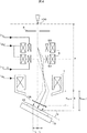
走査コイル9上段の同位置には、チルト(傾斜)角制御用偏向器53が配置され、チルト像および立体像観察時には、一次電子線4を傾斜させ、対物レンズ7の振り戻し作用を用いて、試料10に一次電子線4をチルトさせて照射する。符号34は傾斜角制御用偏向器制御電源である。

Claims (8)
- 荷電粒子源と、前記荷電粒子源から放出される一次荷電粒子線を収束する複数のレンズと、前記一次荷電粒子線を試料上で走査する走査コイルと、前記一次荷電粒子を収束して前記試料に照射する対物レンズと、前記対物レンズよりも上段に配置され、前記一次荷電粒子線をチルトさせる偏向器とを有し、前記対物レンズの振り戻を用いてチルトさせた前記一次荷電粒子線を前記試料に照射することにより、前記試料のチルト像、もしくは左右視差角像を取得する荷電粒子線装置において、
前記対物レンズと前記偏向器の間にアライナーが更に備えられ、
前記アライナーは、前記偏向器のチルト角、前記複数のレンズ条件、前記対物レンズと前記試料までの距離を用いて、前記一次荷電粒子線のチルト時に発生する前記試料の視野ずれを補正するビームチルト視野補正機能を有し、
前記試料の表面傾斜に対応して、前記一次荷電粒子線が前記試料上を1ライン走査中に前記対物レンズの焦点とチルトした前記一次荷電粒子線による視野ずれを同時、連続的に補正する傾斜焦点補正機能を有することを特徴とする荷電粒子線装置。 - 請求項1記載の荷電粒子線装置において、
前記対物レンズの焦点補正とチルトした前記一次荷電粒子線による視野ずれ補正と同時に走査幅を変更し、前記試料表面傾斜を行わない場合と同等の領域を走査する傾斜倍率補正機能を有することを特徴とする荷電粒子線装置。 - 請求項2記載の荷電粒子線装置において、
更に、画像表示装置を備え、
前記画像表示装置は、ビームチルト視野補正、傾斜焦点補正、傾斜倍率補正の3つの内の少なくとも一つを実行可能とする入力手段を含むGUI画面を表示するものであることを特徴とする荷電粒子線装置。 - 荷電粒子源と、試料ステージと、前記荷電粒子源から放出される一次荷電粒子線を収束して光軸上にクロスオーバを形成する複数のレンズと、前記一次荷電粒子を収束して前記試料ステージに載置される試料に照射する対物レンズと、前記対物レンズと前記クロスオーバとの間に配置され、前記一次荷電粒子線をチルトさせる偏向器とを有し、前記一次荷電粒子線を前記偏向器により前記光軸を対称軸として左右にチルトして2本の一次荷電粒子線とし、前記試料の左右のステレオペア画像を取得する荷電粒子線装置において、
前記対物レンズと前記偏向器の間に視野補正用アライナーが更に備えられ、
前記視野補正用アライナーは、前記偏向器により前記一次荷電粒子線をチルトすることにより前記クロスオーバとは異なる位置に形成される仮想的なクロスオーバの前記光軸からの位置ずれを前記光軸と一致するように前記一次荷電粒子線のチルト角度を補正し、表面傾斜試料にかかる前記左右のステレオペア画像の視野を一致させることを特徴とする荷電粒子線装置。 - 請求項4記載の荷電粒子線装置において、
前記一致は、±200μm以内の範囲を許容することを特徴とする荷電粒子線装置。 - 請求項4記載の荷電粒子線装置において、
前記チルト角度の補正角度は、前記偏向器によりチルトされる前記一次荷電粒子線のチルト角度と、前記偏向器と前記視野補正用アライナーとの間の距離と、前記視野補正用アライナーと前記対物レンズとの間の距離と、前記複数のレンズにより形成される前記一次荷電粒子線のクロスオーバと前記対物レンズとの間の距離とを用いて決定されることを特徴とする荷電粒子線装置。 - 荷電粒子源と、試料ステージと、前記ステージを傾斜させる傾斜機構と、前記荷電粒子源から放出される一次荷電粒子線を収束して光軸上にクロスオーバを形成する複数のレンズと、前記一次荷電粒子線を前記試料ステージに載置される試料上で走査する走査コイルと、前記一次荷電粒子を収束して前記試料に照射する対物レンズと、前記対物レンズと前記クロスオーバとの間に配置され、前記一次荷電粒子線をチルトさせる偏向器と、これらを制御する制御CPUと、前記制御CPUに接続された画像表示装置とを有する荷電粒子線装置において、
前記対物レンズと前記偏向器の間に視野補正用アライナーが更に備えられ、
前記傾斜機構を用いて傾斜させた前記試料ステージに載置される前記試料の表面に前記一次荷電粒子線を照射してチルト像を観察する際に、
前記制御CPUは、
前記走査コイルが、傾いた前記試料ステージの傾斜方向に前記一次荷電粒子線を走査するように、かつ、
前記対物レンズが、走査される前記一次荷電粒子線が前記試料の表面において焦点を結ぶように、かつ、
前記視野補正用アライナーが、前記偏向器により前記一次荷電粒子線をチルトすること及び前記対物レンズにより前記一次荷電粒子線の焦点位置を変更することにより前記クロスオーバとは異なる位置に形成される仮想的なクロスオーバの前記光軸からの位置ずれを前記光軸と一致させ前記一次荷電粒子線のチルト角度を補正するように制御するものであることを特徴とする荷電粒子線装置。 - 請求項7記載の荷電粒子線装置において、
前記制御CPUは、更に、
前記傾斜前と等しい走査範囲にて走査を行うように前記走査コイルを制御するものであることを特徴とする荷電粒子線装置。
Priority Applications (6)
| Application Number | Priority Date | Filing Date | Title |
|---|---|---|---|
| JP2011012435A JP5364112B2 (ja) | 2011-01-25 | 2011-01-25 | 荷電粒子線装置 |
| US13/979,964 US9287083B2 (en) | 2011-01-25 | 2011-12-16 | Charged particle beam device |
| CN201180065868.4A CN103348437B (zh) | 2011-01-25 | 2011-12-16 | 带电粒子束装置 |
| DE112011104595.6T DE112011104595B4 (de) | 2011-01-25 | 2011-12-16 | Vorrichtung mit einem geladenen Teilchenstrahl sowie Verfahren zur Steuerung |
| KR1020137018107A KR101470270B1 (ko) | 2011-01-25 | 2011-12-16 | 하전 입자선 장치 |
| PCT/JP2011/079166 WO2012101927A1 (ja) | 2011-01-25 | 2011-12-16 | 荷電粒子線装置 |
Applications Claiming Priority (1)
| Application Number | Priority Date | Filing Date | Title |
|---|---|---|---|
| JP2011012435A JP5364112B2 (ja) | 2011-01-25 | 2011-01-25 | 荷電粒子線装置 |
Publications (2)
| Publication Number | Publication Date |
|---|---|
| JP2012155911A JP2012155911A (ja) | 2012-08-16 |
| JP5364112B2 true JP5364112B2 (ja) | 2013-12-11 |
Family
ID=46580510
Family Applications (1)
| Application Number | Title | Priority Date | Filing Date |
|---|---|---|---|
| JP2011012435A Expired - Fee Related JP5364112B2 (ja) | 2011-01-25 | 2011-01-25 | 荷電粒子線装置 |
Country Status (6)
| Country | Link |
|---|---|
| US (1) | US9287083B2 (ja) |
| JP (1) | JP5364112B2 (ja) |
| KR (1) | KR101470270B1 (ja) |
| CN (1) | CN103348437B (ja) |
| DE (1) | DE112011104595B4 (ja) |
| WO (1) | WO2012101927A1 (ja) |
Families Citing this family (11)
| Publication number | Priority date | Publication date | Assignee | Title |
|---|---|---|---|---|
| JP5331780B2 (ja) * | 2010-11-30 | 2013-10-30 | 株式会社日立ハイテクノロジーズ | 電子顕微鏡,電子顕微鏡用画像再構成システム、および電子顕微鏡用画像再構成方法 |
| JP5698157B2 (ja) | 2012-01-06 | 2015-04-08 | 株式会社日立ハイテクノロジーズ | 荷電粒子線装置および傾斜観察画像表示方法 |
| JP6022344B2 (ja) * | 2012-12-21 | 2016-11-09 | 株式会社日立ハイテクノロジーズ | 演算装置及び荷電粒子線応用装置 |
| JP6165643B2 (ja) * | 2014-01-23 | 2017-07-19 | 株式会社日立ハイテクサイエンス | 荷電粒子ビーム装置、荷電粒子ビーム装置の制御方法及び断面加工観察装置 |
| US10593514B2 (en) * | 2015-06-08 | 2020-03-17 | Nikon Corporation | Charged particle beam irradiation apparatus and device manufacturing method |
| DE112016005577B4 (de) | 2016-01-29 | 2021-09-16 | Hitachi High-Tech Corporation | Ladungsträgerstrahlvorrichtung und Verfahren zur Einstellung ihrer optischen Achse |
| JP6743787B2 (ja) * | 2017-09-13 | 2020-08-19 | 株式会社ニューフレアテクノロジー | 荷電粒子ビーム描画装置及びブランキング回路の故障診断方法 |
| JP6930431B2 (ja) * | 2018-01-10 | 2021-09-01 | 株式会社ニューフレアテクノロジー | アパーチャのアライメント方法及びマルチ荷電粒子ビーム描画装置 |
| JP7047523B2 (ja) * | 2018-03-26 | 2022-04-05 | 株式会社島津製作所 | 荷電粒子ビーム軸合わせ装置、荷電粒子ビーム照射装置および荷電粒子ビーム軸合わせ方法 |
| US10504684B1 (en) * | 2018-07-12 | 2019-12-10 | ICT Integrated Circuit Testing Gesellschaft für Halbleiterprüftechnik mbH | High performance inspection scanning electron microscope device and method of operating the same |
| CN115497793B (zh) * | 2022-10-20 | 2023-08-22 | 国仪量子(合肥)技术有限公司 | 扫描电镜及其控制方法、控制装置和存储介质 |
Family Cites Families (27)
| Publication number | Priority date | Publication date | Assignee | Title |
|---|---|---|---|---|
| NL7012671A (ja) | 1970-08-27 | 1972-02-29 | ||
| JPS60200450A (ja) | 1984-03-26 | 1985-10-09 | Hitachi Ltd | 走査形電子顕微鏡 |
| US5338839A (en) | 1988-04-12 | 1994-08-16 | Massachusetts Institute Of Technology | DNA encoding nestin protein |
| JPH0233843A (ja) | 1988-07-25 | 1990-02-05 | Hitachi Ltd | 走査電子顕微鏡 |
| JP2509075Y2 (ja) * | 1988-09-26 | 1996-08-28 | 北川工業株式会社 | 雑音電流吸収具 |
| US5338939A (en) * | 1992-01-13 | 1994-08-16 | Fujitsu Limited | Charged particle beam exposure including a heat blocking partition positioned near deflecting coils |
| JPH05258700A (ja) * | 1992-03-13 | 1993-10-08 | Jeol Ltd | 走査像観察方法および走査電子顕微鏡 |
| US5414261A (en) * | 1993-07-01 | 1995-05-09 | The Regents Of The University Of California | Enhanced imaging mode for transmission electron microscopy |
| JP3654022B2 (ja) | 1998-12-25 | 2005-06-02 | 株式会社日立製作所 | 荷電粒子線装置 |
| JP2001273861A (ja) * | 2000-03-28 | 2001-10-05 | Toshiba Corp | 荷電ビーム装置およびパターン傾斜観察方法 |
| JP2002343293A (ja) | 2001-05-17 | 2002-11-29 | Hitachi Ltd | 走査形電子顕微鏡装置 |
| JP2003100246A (ja) * | 2001-09-25 | 2003-04-04 | Toshiba Corp | 荷電ビーム装置並びにパターン測定方法およびパターン描画方法 |
| JP4094042B2 (ja) | 2002-09-11 | 2008-06-04 | 株式会社日立ハイテクノロジーズ | 荷電粒子線装置及び荷電粒子線照射方法 |
| JP3968334B2 (ja) * | 2002-09-11 | 2007-08-29 | 株式会社日立ハイテクノロジーズ | 荷電粒子線装置及び荷電粒子線照射方法 |
| US7067808B2 (en) * | 2003-10-14 | 2006-06-27 | Topcon Corporation | Electron beam system and electron beam measuring and observing method |
| JP4229799B2 (ja) | 2003-10-14 | 2009-02-25 | 株式会社トプコン | 電子線測定または観察装置、電子線測定または観察方法 |
| JP4383950B2 (ja) | 2004-04-23 | 2009-12-16 | 株式会社日立ハイテクノロジーズ | 荷電粒子線調整方法、及び荷電粒子線装置 |
| US7075093B2 (en) * | 2004-05-12 | 2006-07-11 | Gorski Richard M | Parallel multi-electron beam lithography for IC fabrication with precise X-Y translation |
| JP4620981B2 (ja) * | 2004-08-10 | 2011-01-26 | 株式会社日立ハイテクノロジーズ | 荷電粒子ビーム装置 |
| JP4857101B2 (ja) * | 2006-12-21 | 2012-01-18 | 株式会社日立ハイテクノロジーズ | プローブ評価方法 |
| CZ298798B6 (cs) | 2007-07-30 | 2008-01-30 | Tescan, S. R. O. | Zarízení pro prostorové zobrazování vzorku v reálném case |
| JP5028297B2 (ja) * | 2008-02-22 | 2012-09-19 | 株式会社日立ハイテクノロジーズ | 収差補正器を備えた荷電粒子線装置 |
| JP2009205904A (ja) * | 2008-02-27 | 2009-09-10 | Hitachi High-Technologies Corp | 冷陰極型電界放出電子銃及びそれを用いた電子線装置 |
| JP5183318B2 (ja) * | 2008-06-26 | 2013-04-17 | 株式会社日立ハイテクノロジーズ | 荷電粒子線装置 |
| JP4431624B2 (ja) | 2008-08-25 | 2010-03-17 | 株式会社日立ハイテクノロジーズ | 荷電粒子線調整方法、及び荷電粒子線装置 |
| JP2010016007A (ja) | 2009-10-22 | 2010-01-21 | Hitachi High-Technologies Corp | 荷電粒子線調整方法及び荷電粒子線装置 |
| DE102009052392A1 (de) * | 2009-11-09 | 2011-12-15 | Carl Zeiss Nts Gmbh | SACP-Verfahren und teilchenoptisches System zur Ausführung eines solchen Verfahrens |
-
2011
- 2011-01-25 JP JP2011012435A patent/JP5364112B2/ja not_active Expired - Fee Related
- 2011-12-16 CN CN201180065868.4A patent/CN103348437B/zh not_active Expired - Fee Related
- 2011-12-16 US US13/979,964 patent/US9287083B2/en not_active Expired - Fee Related
- 2011-12-16 WO PCT/JP2011/079166 patent/WO2012101927A1/ja not_active Ceased
- 2011-12-16 KR KR1020137018107A patent/KR101470270B1/ko not_active Expired - Fee Related
- 2011-12-16 DE DE112011104595.6T patent/DE112011104595B4/de not_active Expired - Fee Related
Also Published As
| Publication number | Publication date |
|---|---|
| DE112011104595T5 (de) | 2014-01-16 |
| CN103348437B (zh) | 2014-10-29 |
| CN103348437A (zh) | 2013-10-09 |
| US20130299715A1 (en) | 2013-11-14 |
| KR20130112921A (ko) | 2013-10-14 |
| KR101470270B1 (ko) | 2014-12-05 |
| DE112011104595B4 (de) | 2015-10-01 |
| JP2012155911A (ja) | 2012-08-16 |
| US9287083B2 (en) | 2016-03-15 |
| WO2012101927A1 (ja) | 2012-08-02 |
Similar Documents
| Publication | Publication Date | Title |
|---|---|---|
| JP5364112B2 (ja) | 荷電粒子線装置 | |
| JP4383950B2 (ja) | 荷電粒子線調整方法、及び荷電粒子線装置 | |
| JP5792509B2 (ja) | 荷電粒子ビーム装置及び試料加工方法 | |
| US9012842B2 (en) | Charged particle beam device and inclined observation image display method | |
| US8143573B2 (en) | Charged particle beam apparatus | |
| JP6620170B2 (ja) | 荷電粒子線装置およびその光軸調整方法 | |
| JP6647854B2 (ja) | 収差補正方法および荷電粒子線装置 | |
| JP2006012664A (ja) | 荷電粒子線装置及びその光軸調整方法 | |
| JP2011054426A (ja) | 荷電粒子ビーム照射装置及び該装置の軸合わせ調整方法 | |
| JP2003168383A (ja) | 走査電子顕微鏡装置 | |
| US12261013B2 (en) | Charged particle beam system and control method therefor | |
| KR102628711B1 (ko) | 하전 입자선 장치 | |
| TW202036636A (zh) | 荷電粒子束裝置 | |
| WO2021100172A1 (ja) | 荷電粒子線装置及び収差補正方法 | |
| TWI748527B (zh) | 荷電粒子束裝置 | |
| JP4431624B2 (ja) | 荷電粒子線調整方法、及び荷電粒子線装置 | |
| JP6959969B2 (ja) | 荷電粒子線装置 | |
| JP2004146192A (ja) | 透過電子顕微鏡による試料観察方法 | |
| JP2010016007A (ja) | 荷電粒子線調整方法及び荷電粒子線装置 | |
| JP2011238635A (ja) | 走査荷電粒子線装置 | |
| JP2009135119A (ja) | 荷電粒子線装置の光軸調整方法 |
Legal Events
| Date | Code | Title | Description |
|---|---|---|---|
| A621 | Written request for application examination |
Free format text: JAPANESE INTERMEDIATE CODE: A621 Effective date: 20130215 |
|
| A131 | Notification of reasons for refusal |
Free format text: JAPANESE INTERMEDIATE CODE: A131 Effective date: 20130604 |
|
| A521 | Request for written amendment filed |
Free format text: JAPANESE INTERMEDIATE CODE: A523 Effective date: 20130801 |
|
| TRDD | Decision of grant or rejection written | ||
| A01 | Written decision to grant a patent or to grant a registration (utility model) |
Free format text: JAPANESE INTERMEDIATE CODE: A01 Effective date: 20130827 |
|
| A61 | First payment of annual fees (during grant procedure) |
Free format text: JAPANESE INTERMEDIATE CODE: A61 Effective date: 20130906 |
|
| R150 | Certificate of patent or registration of utility model |
Ref document number: 5364112 Country of ref document: JP Free format text: JAPANESE INTERMEDIATE CODE: R150 Free format text: JAPANESE INTERMEDIATE CODE: R150 |
|
| S531 | Written request for registration of change of domicile |
Free format text: JAPANESE INTERMEDIATE CODE: R313531 |
|
| S533 | Written request for registration of change of name |
Free format text: JAPANESE INTERMEDIATE CODE: R313533 |
|
| R350 | Written notification of registration of transfer |
Free format text: JAPANESE INTERMEDIATE CODE: R350 |
|
| LAPS | Cancellation because of no payment of annual fees |