JP5345552B2 - 複数の窒化物ナノワイヤとその製造方法 - Google Patents
複数の窒化物ナノワイヤとその製造方法 Download PDFInfo
- Publication number
- JP5345552B2 JP5345552B2 JP2009545523A JP2009545523A JP5345552B2 JP 5345552 B2 JP5345552 B2 JP 5345552B2 JP 2009545523 A JP2009545523 A JP 2009545523A JP 2009545523 A JP2009545523 A JP 2009545523A JP 5345552 B2 JP5345552 B2 JP 5345552B2
- Authority
- JP
- Japan
- Prior art keywords
- growth
- nanowire
- nitride
- nanowires
- growing
- Prior art date
- Legal status (The legal status is an assumption and is not a legal conclusion. Google has not performed a legal analysis and makes no representation as to the accuracy of the status listed.)
- Expired - Fee Related
Links
Images


Classifications
-
- B—PERFORMING OPERATIONS; TRANSPORTING
- B82—NANOTECHNOLOGY
- B82B—NANOSTRUCTURES FORMED BY MANIPULATION OF INDIVIDUAL ATOMS, MOLECULES, OR LIMITED COLLECTIONS OF ATOMS OR MOLECULES AS DISCRETE UNITS; MANUFACTURE OR TREATMENT THEREOF
- B82B1/00—Nanostructures formed by manipulation of individual atoms or molecules, or limited collections of atoms or molecules as discrete units
-
- H—ELECTRICITY
- H10—SEMICONDUCTOR DEVICES; ELECTRIC SOLID-STATE DEVICES NOT OTHERWISE PROVIDED FOR
- H10H—INORGANIC LIGHT-EMITTING SEMICONDUCTOR DEVICES HAVING POTENTIAL BARRIERS
- H10H20/00—Individual inorganic light-emitting semiconductor devices having potential barriers, e.g. light-emitting diodes [LED]
- H10H20/80—Constructional details
- H10H20/81—Bodies
- H10H20/822—Materials of the light-emitting regions
- H10H20/824—Materials of the light-emitting regions comprising only Group III-V materials, e.g. GaP
- H10H20/825—Materials of the light-emitting regions comprising only Group III-V materials, e.g. GaP containing nitrogen, e.g. GaN
-
- B—PERFORMING OPERATIONS; TRANSPORTING
- B82—NANOTECHNOLOGY
- B82B—NANOSTRUCTURES FORMED BY MANIPULATION OF INDIVIDUAL ATOMS, MOLECULES, OR LIMITED COLLECTIONS OF ATOMS OR MOLECULES AS DISCRETE UNITS; MANUFACTURE OR TREATMENT THEREOF
- B82B3/00—Manufacture or treatment of nanostructures by manipulation of individual atoms or molecules, or limited collections of atoms or molecules as discrete units
-
- B—PERFORMING OPERATIONS; TRANSPORTING
- B82—NANOTECHNOLOGY
- B82Y—SPECIFIC USES OR APPLICATIONS OF NANOSTRUCTURES; MEASUREMENT OR ANALYSIS OF NANOSTRUCTURES; MANUFACTURE OR TREATMENT OF NANOSTRUCTURES
- B82Y10/00—Nanotechnology for information processing, storage or transmission, e.g. quantum computing or single electron logic
-
- C—CHEMISTRY; METALLURGY
- C30—CRYSTAL GROWTH
- C30B—SINGLE-CRYSTAL GROWTH; UNIDIRECTIONAL SOLIDIFICATION OF EUTECTIC MATERIAL OR UNIDIRECTIONAL DEMIXING OF EUTECTOID MATERIAL; REFINING BY ZONE-MELTING OF MATERIAL; PRODUCTION OF A HOMOGENEOUS POLYCRYSTALLINE MATERIAL WITH DEFINED STRUCTURE; SINGLE CRYSTALS OR HOMOGENEOUS POLYCRYSTALLINE MATERIAL WITH DEFINED STRUCTURE; AFTER-TREATMENT OF SINGLE CRYSTALS OR A HOMOGENEOUS POLYCRYSTALLINE MATERIAL WITH DEFINED STRUCTURE; APPARATUS THEREFOR
- C30B25/00—Single-crystal growth by chemical reaction of reactive gases, e.g. chemical vapour-deposition growth
-
- C—CHEMISTRY; METALLURGY
- C30—CRYSTAL GROWTH
- C30B—SINGLE-CRYSTAL GROWTH; UNIDIRECTIONAL SOLIDIFICATION OF EUTECTIC MATERIAL OR UNIDIRECTIONAL DEMIXING OF EUTECTOID MATERIAL; REFINING BY ZONE-MELTING OF MATERIAL; PRODUCTION OF A HOMOGENEOUS POLYCRYSTALLINE MATERIAL WITH DEFINED STRUCTURE; SINGLE CRYSTALS OR HOMOGENEOUS POLYCRYSTALLINE MATERIAL WITH DEFINED STRUCTURE; AFTER-TREATMENT OF SINGLE CRYSTALS OR A HOMOGENEOUS POLYCRYSTALLINE MATERIAL WITH DEFINED STRUCTURE; APPARATUS THEREFOR
- C30B29/00—Single crystals or homogeneous polycrystalline material with defined structure characterised by the material or by their shape
- C30B29/10—Inorganic compounds or compositions
- C30B29/40—AIIIBV compounds wherein A is B, Al, Ga, In or Tl and B is N, P, As, Sb or Bi
- C30B29/403—AIII-nitrides
- C30B29/406—Gallium nitride
-
- C—CHEMISTRY; METALLURGY
- C30—CRYSTAL GROWTH
- C30B—SINGLE-CRYSTAL GROWTH; UNIDIRECTIONAL SOLIDIFICATION OF EUTECTIC MATERIAL OR UNIDIRECTIONAL DEMIXING OF EUTECTOID MATERIAL; REFINING BY ZONE-MELTING OF MATERIAL; PRODUCTION OF A HOMOGENEOUS POLYCRYSTALLINE MATERIAL WITH DEFINED STRUCTURE; SINGLE CRYSTALS OR HOMOGENEOUS POLYCRYSTALLINE MATERIAL WITH DEFINED STRUCTURE; AFTER-TREATMENT OF SINGLE CRYSTALS OR A HOMOGENEOUS POLYCRYSTALLINE MATERIAL WITH DEFINED STRUCTURE; APPARATUS THEREFOR
- C30B29/00—Single crystals or homogeneous polycrystalline material with defined structure characterised by the material or by their shape
- C30B29/60—Single crystals or homogeneous polycrystalline material with defined structure characterised by the material or by their shape characterised by shape
-
- H—ELECTRICITY
- H10—SEMICONDUCTOR DEVICES; ELECTRIC SOLID-STATE DEVICES NOT OTHERWISE PROVIDED FOR
- H10D—INORGANIC ELECTRIC SEMICONDUCTOR DEVICES
- H10D62/00—Semiconductor bodies, or regions thereof, of devices having potential barriers
- H10D62/10—Shapes, relative sizes or dispositions of the regions of the semiconductor bodies; Shapes of the semiconductor bodies
- H10D62/117—Shapes of semiconductor bodies
- H10D62/118—Nanostructure semiconductor bodies
- H10D62/119—Nanowire, nanosheet or nanotube semiconductor bodies
- H10D62/121—Nanowire, nanosheet or nanotube semiconductor bodies oriented parallel to substrates
-
- H—ELECTRICITY
- H10—SEMICONDUCTOR DEVICES; ELECTRIC SOLID-STATE DEVICES NOT OTHERWISE PROVIDED FOR
- H10D—INORGANIC ELECTRIC SEMICONDUCTOR DEVICES
- H10D62/00—Semiconductor bodies, or regions thereof, of devices having potential barriers
- H10D62/10—Shapes, relative sizes or dispositions of the regions of the semiconductor bodies; Shapes of the semiconductor bodies
- H10D62/117—Shapes of semiconductor bodies
- H10D62/118—Nanostructure semiconductor bodies
- H10D62/119—Nanowire, nanosheet or nanotube semiconductor bodies
- H10D62/122—Nanowire, nanosheet or nanotube semiconductor bodies oriented at angles to substrates, e.g. perpendicular to substrates
-
- H—ELECTRICITY
- H10—SEMICONDUCTOR DEVICES; ELECTRIC SOLID-STATE DEVICES NOT OTHERWISE PROVIDED FOR
- H10D—INORGANIC ELECTRIC SEMICONDUCTOR DEVICES
- H10D62/00—Semiconductor bodies, or regions thereof, of devices having potential barriers
- H10D62/80—Semiconductor bodies, or regions thereof, of devices having potential barriers characterised by the materials
- H10D62/85—Semiconductor bodies, or regions thereof, of devices having potential barriers characterised by the materials being Group III-V materials, e.g. GaAs
- H10D62/8503—Nitride Group III-V materials, e.g. AlN or GaN
-
- H—ELECTRICITY
- H10—SEMICONDUCTOR DEVICES; ELECTRIC SOLID-STATE DEVICES NOT OTHERWISE PROVIDED FOR
- H10H—INORGANIC LIGHT-EMITTING SEMICONDUCTOR DEVICES HAVING POTENTIAL BARRIERS
- H10H20/00—Individual inorganic light-emitting semiconductor devices having potential barriers, e.g. light-emitting diodes [LED]
- H10H20/01—Manufacture or treatment
- H10H20/011—Manufacture or treatment of bodies, e.g. forming semiconductor layers
- H10H20/013—Manufacture or treatment of bodies, e.g. forming semiconductor layers having light-emitting regions comprising only Group III-V materials
- H10H20/0137—Manufacture or treatment of bodies, e.g. forming semiconductor layers having light-emitting regions comprising only Group III-V materials the light-emitting regions comprising nitride materials
-
- H—ELECTRICITY
- H10—SEMICONDUCTOR DEVICES; ELECTRIC SOLID-STATE DEVICES NOT OTHERWISE PROVIDED FOR
- H10H—INORGANIC LIGHT-EMITTING SEMICONDUCTOR DEVICES HAVING POTENTIAL BARRIERS
- H10H20/00—Individual inorganic light-emitting semiconductor devices having potential barriers, e.g. light-emitting diodes [LED]
- H10H20/01—Manufacture or treatment
- H10H20/011—Manufacture or treatment of bodies, e.g. forming semiconductor layers
- H10H20/018—Bonding of wafers
-
- H—ELECTRICITY
- H10—SEMICONDUCTOR DEVICES; ELECTRIC SOLID-STATE DEVICES NOT OTHERWISE PROVIDED FOR
- H10H—INORGANIC LIGHT-EMITTING SEMICONDUCTOR DEVICES HAVING POTENTIAL BARRIERS
- H10H20/00—Individual inorganic light-emitting semiconductor devices having potential barriers, e.g. light-emitting diodes [LED]
- H10H20/80—Constructional details
- H10H20/81—Bodies
- H10H20/811—Bodies having quantum effect structures or superlattices, e.g. tunnel junctions
- H10H20/812—Bodies having quantum effect structures or superlattices, e.g. tunnel junctions within the light-emitting regions, e.g. having quantum confinement structures
-
- H—ELECTRICITY
- H10—SEMICONDUCTOR DEVICES; ELECTRIC SOLID-STATE DEVICES NOT OTHERWISE PROVIDED FOR
- H10H—INORGANIC LIGHT-EMITTING SEMICONDUCTOR DEVICES HAVING POTENTIAL BARRIERS
- H10H20/00—Individual inorganic light-emitting semiconductor devices having potential barriers, e.g. light-emitting diodes [LED]
- H10H20/80—Constructional details
- H10H20/81—Bodies
- H10H20/819—Bodies characterised by their shape, e.g. curved or truncated substrates
- H10H20/821—Bodies characterised by their shape, e.g. curved or truncated substrates of the light-emitting regions, e.g. non-planar junctions
-
- H—ELECTRICITY
- H10—SEMICONDUCTOR DEVICES; ELECTRIC SOLID-STATE DEVICES NOT OTHERWISE PROVIDED FOR
- H10P—GENERIC PROCESSES OR APPARATUS FOR THE MANUFACTURE OR TREATMENT OF DEVICES COVERED BY CLASS H10
- H10P14/00—Formation of materials, e.g. in the shape of layers or pillars
- H10P14/20—Formation of materials, e.g. in the shape of layers or pillars of semiconductor materials
- H10P14/24—Formation of materials, e.g. in the shape of layers or pillars of semiconductor materials using chemical vapour deposition [CVD]
-
- H—ELECTRICITY
- H10—SEMICONDUCTOR DEVICES; ELECTRIC SOLID-STATE DEVICES NOT OTHERWISE PROVIDED FOR
- H10P—GENERIC PROCESSES OR APPARATUS FOR THE MANUFACTURE OR TREATMENT OF DEVICES COVERED BY CLASS H10
- H10P14/00—Formation of materials, e.g. in the shape of layers or pillars
- H10P14/20—Formation of materials, e.g. in the shape of layers or pillars of semiconductor materials
- H10P14/27—Formation of materials, e.g. in the shape of layers or pillars of semiconductor materials using selective deposition, e.g. simultaneous growth of monocrystalline and non-monocrystalline semiconductor materials
- H10P14/271—Formation of materials, e.g. in the shape of layers or pillars of semiconductor materials using selective deposition, e.g. simultaneous growth of monocrystalline and non-monocrystalline semiconductor materials characterised by the preparation of substrate for selective deposition
-
- H—ELECTRICITY
- H10—SEMICONDUCTOR DEVICES; ELECTRIC SOLID-STATE DEVICES NOT OTHERWISE PROVIDED FOR
- H10P—GENERIC PROCESSES OR APPARATUS FOR THE MANUFACTURE OR TREATMENT OF DEVICES COVERED BY CLASS H10
- H10P14/00—Formation of materials, e.g. in the shape of layers or pillars
- H10P14/20—Formation of materials, e.g. in the shape of layers or pillars of semiconductor materials
- H10P14/32—Formation of materials, e.g. in the shape of layers or pillars of semiconductor materials characterised by intermediate layers between substrates and deposited layers
- H10P14/3202—Materials thereof
- H10P14/3214—Materials thereof being Group IIIA-VA semiconductors
- H10P14/3216—Nitrides
-
- H—ELECTRICITY
- H10—SEMICONDUCTOR DEVICES; ELECTRIC SOLID-STATE DEVICES NOT OTHERWISE PROVIDED FOR
- H10P—GENERIC PROCESSES OR APPARATUS FOR THE MANUFACTURE OR TREATMENT OF DEVICES COVERED BY CLASS H10
- H10P14/00—Formation of materials, e.g. in the shape of layers or pillars
- H10P14/20—Formation of materials, e.g. in the shape of layers or pillars of semiconductor materials
- H10P14/34—Deposited materials, e.g. layers
- H10P14/3402—Deposited materials, e.g. layers characterised by the chemical composition
- H10P14/3414—Deposited materials, e.g. layers characterised by the chemical composition being group IIIA-VIA materials
- H10P14/3416—Nitrides
-
- H—ELECTRICITY
- H10—SEMICONDUCTOR DEVICES; ELECTRIC SOLID-STATE DEVICES NOT OTHERWISE PROVIDED FOR
- H10P—GENERIC PROCESSES OR APPARATUS FOR THE MANUFACTURE OR TREATMENT OF DEVICES COVERED BY CLASS H10
- H10P14/00—Formation of materials, e.g. in the shape of layers or pillars
- H10P14/20—Formation of materials, e.g. in the shape of layers or pillars of semiconductor materials
- H10P14/34—Deposited materials, e.g. layers
- H10P14/3451—Structure
- H10P14/3452—Microstructure
- H10P14/3462—Nanowires
-
- B—PERFORMING OPERATIONS; TRANSPORTING
- B82—NANOTECHNOLOGY
- B82Y—SPECIFIC USES OR APPLICATIONS OF NANOSTRUCTURES; MEASUREMENT OR ANALYSIS OF NANOSTRUCTURES; MANUFACTURE OR TREATMENT OF NANOSTRUCTURES
- B82Y40/00—Manufacture or treatment of nanostructures
-
- H—ELECTRICITY
- H10—SEMICONDUCTOR DEVICES; ELECTRIC SOLID-STATE DEVICES NOT OTHERWISE PROVIDED FOR
- H10H—INORGANIC LIGHT-EMITTING SEMICONDUCTOR DEVICES HAVING POTENTIAL BARRIERS
- H10H20/00—Individual inorganic light-emitting semiconductor devices having potential barriers, e.g. light-emitting diodes [LED]
- H10H20/01—Manufacture or treatment
- H10H20/011—Manufacture or treatment of bodies, e.g. forming semiconductor layers
- H10H20/013—Manufacture or treatment of bodies, e.g. forming semiconductor layers having light-emitting regions comprising only Group III-V materials
- H10H20/0133—Manufacture or treatment of bodies, e.g. forming semiconductor layers having light-emitting regions comprising only Group III-V materials with a substrate not being Group III-V materials
- H10H20/01335—Manufacture or treatment of bodies, e.g. forming semiconductor layers having light-emitting regions comprising only Group III-V materials with a substrate not being Group III-V materials the light-emitting regions comprising nitride materials
-
- H—ELECTRICITY
- H10—SEMICONDUCTOR DEVICES; ELECTRIC SOLID-STATE DEVICES NOT OTHERWISE PROVIDED FOR
- H10H—INORGANIC LIGHT-EMITTING SEMICONDUCTOR DEVICES HAVING POTENTIAL BARRIERS
- H10H20/00—Individual inorganic light-emitting semiconductor devices having potential barriers, e.g. light-emitting diodes [LED]
- H10H20/80—Constructional details
- H10H20/81—Bodies
- H10H20/817—Bodies characterised by the crystal structures or orientations, e.g. polycrystalline, amorphous or porous
- H10H20/818—Bodies characterised by the crystal structures or orientations, e.g. polycrystalline, amorphous or porous within the light-emitting regions
-
- Y—GENERAL TAGGING OF NEW TECHNOLOGICAL DEVELOPMENTS; GENERAL TAGGING OF CROSS-SECTIONAL TECHNOLOGIES SPANNING OVER SEVERAL SECTIONS OF THE IPC; TECHNICAL SUBJECTS COVERED BY FORMER USPC CROSS-REFERENCE ART COLLECTIONS [XRACs] AND DIGESTS
- Y10—TECHNICAL SUBJECTS COVERED BY FORMER USPC
- Y10S—TECHNICAL SUBJECTS COVERED BY FORMER USPC CROSS-REFERENCE ART COLLECTIONS [XRACs] AND DIGESTS
- Y10S977/00—Nanotechnology
- Y10S977/902—Specified use of nanostructure
- Y10S977/932—Specified use of nanostructure for electronic or optoelectronic application
Landscapes
- Chemical & Material Sciences (AREA)
- Engineering & Computer Science (AREA)
- Crystallography & Structural Chemistry (AREA)
- Nanotechnology (AREA)
- Organic Chemistry (AREA)
- Materials Engineering (AREA)
- Metallurgy (AREA)
- Chemical Kinetics & Catalysis (AREA)
- General Chemical & Material Sciences (AREA)
- Inorganic Chemistry (AREA)
- Physics & Mathematics (AREA)
- Mathematical Physics (AREA)
- Theoretical Computer Science (AREA)
- Manufacturing & Machinery (AREA)
- Crystals, And After-Treatments Of Crystals (AREA)
- Led Devices (AREA)
Description
報告された業績は、この技術の素晴らしい潜在能力を示すが、積層欠陥や転位などの結晶欠陥なしにエピタキシァルで垂直方向に直立するGaN膜ナノワイヤを製造する方法を提供するために、および、工業的製造までスケールアップするためによく適合した方法を提供するために、改良が必要である。
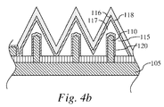
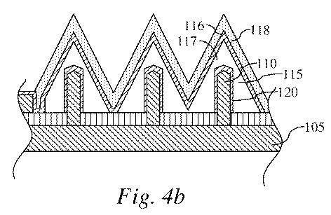
a)基板105上に成長マスク111を提供する。基板は、例えば、GaNであり、成長マスクはSiNxまたはSiOxなどである。
b)成長マスク中に複数の開口部113を生成する。複数の開口部は、好ましくは、開口部直径と開口部の相対的な位置の両方に対してよく制御されている。この手順に対して、当技術分野で知られている電子線リソグラフィー(EBL)、ナノインプリントリゾグラフィ、光学リソグラフィー、および反応イオンエッチング(RIE)または湿式化学的エッチング方法を含むいくつかの技術は、限定無しに利用することができる。好ましくは、複数の開口部の直径は100nmであり、0.5〜5μmのピッチ間隔を有する。複数の開口部は、生成するナノワイヤ105の位置と直径とを画定する。
c)CVD(化学蒸着法)によるナノワイヤの成長は、プレカーサ源流量が連続して存在しているプロセスに基づいている。プレカーサ源流量は、成長ゾーン中で低い過飽和度を達成するように調整されている。V/III比は、1〜100の範囲、好ましくは、1〜50の範囲、さらに好ましくは、5〜50の範囲である。このV/III比は、膜成長のために使用されるV/III比よりかなり低いものであることに注意すべきである。
Claims (10)
- 選択領域を成長させる技術をベースとする化学蒸着法(CVD)を利用して複数の窒化基半導体のナノワイヤを成長させる方法であって、
ナノワイヤの成長工程中に窒素源と有機金属源とが存在し、
前記方法は、
(a)基板(110)上に成長マスク(111)を提供する提供工程と、
(b)前記成長マスク(111)中に複数の開口(113)を生成する生成工程と、
(c)複数のナノワイヤを成長させる成長工程と、
を有し、
前記窒素源と前記有機金属のプレカーサ源とが連続して流れており、
前記方法は、前記ナノワイヤを成長させる成長工程(c)の後に、前記複数のナノワイヤ上にシェル層を形成する少なくとも1つの成長工程を含む平らな成長工程を実施する工程をさらに有し、
前記平らな成長工程中のV/III比は、前記ナノワイヤ成長工程のV/III比よりも高い、ことを特徴とする方法。 - 窒素源の流量と金属有機源の流量との比であるV/III比が1〜100の範囲内であることを特徴とする請求項1に記載の窒化基半導体のナノワイヤを成長させる方法。
- 前記V/III比が1〜50の範囲内であることを特徴とする請求項2に記載の窒化基半導体のナノワイヤを成長させる方法。
- 前記V/III比が5〜50の範囲内であることを特徴とする請求項3に記載の窒化基半導体のナノワイヤを成長させる方法。
- 前記V/III比が前記ナノワイヤの成長工程中、一定であることを特徴とする請求項1乃至請求項4のうちのいずれか1項に記載の窒化基半導体のナノワイヤを成長させる方法。
- 前記窒化基半導体がGaNであり、前記窒素源がアンモニア(NH3)であり、前記有機金属源がトリメチルガリウム(TMG)であることを特徴とする請求項1乃至請求項5のうちのいずれか1項に記載の窒化基半導体のナノワイヤを成長させる方法。
- 前記窒素源と前記有機金属のプレカーサ源とのうちの少なくとも1つが流れているが、ナノワイヤの成長が全く現れないような条件に調整されている前処理工程(C’)をさらに有することを特徴とする請求項1に記載の窒化基半導体のナノワイヤを成長させる方法。
- 前記前処理工程(C’)は、アニーリング工程を含むことを特徴とする請求項7に記載の窒化基半導体のナノワイヤを成長させる方法。
- 前記平らな成長工程のV/III比は、前記ナノワイヤ成長工程のV/III比よりも少なくとも10倍高いことを特徴とする請求項1に記載の窒化基半導体のナノワイヤを成長させる方法。
- 前記窒化基半導体のナノワイヤの成長条件を安定させるために、ドーピング源を導入することを特徴とする請求項1乃至請求項9のうちのいずれか1項に記載の窒化基半導体のナノワイヤを成長させる方法。
Applications Claiming Priority (3)
| Application Number | Priority Date | Filing Date | Title |
|---|---|---|---|
| SE0700102-7 | 2007-01-12 | ||
| SE0700102 | 2007-01-12 | ||
| PCT/SE2008/050036 WO2008085129A1 (en) | 2007-01-12 | 2008-01-14 | Nitride nanowires and method of producing such |
Related Child Applications (1)
| Application Number | Title | Priority Date | Filing Date |
|---|---|---|---|
| JP2013168662A Division JP5807044B2 (ja) | 2007-01-12 | 2013-08-14 | 複数の窒化物ナノワイヤの製造方法 |
Publications (2)
| Publication Number | Publication Date |
|---|---|
| JP2010515651A JP2010515651A (ja) | 2010-05-13 |
| JP5345552B2 true JP5345552B2 (ja) | 2013-11-20 |
Family
ID=39608903
Family Applications (2)
| Application Number | Title | Priority Date | Filing Date |
|---|---|---|---|
| JP2009545523A Expired - Fee Related JP5345552B2 (ja) | 2007-01-12 | 2008-01-14 | 複数の窒化物ナノワイヤとその製造方法 |
| JP2013168662A Expired - Fee Related JP5807044B2 (ja) | 2007-01-12 | 2013-08-14 | 複数の窒化物ナノワイヤの製造方法 |
Family Applications After (1)
| Application Number | Title | Priority Date | Filing Date |
|---|---|---|---|
| JP2013168662A Expired - Fee Related JP5807044B2 (ja) | 2007-01-12 | 2013-08-14 | 複数の窒化物ナノワイヤの製造方法 |
Country Status (8)
| Country | Link |
|---|---|
| US (6) | US7829443B2 (ja) |
| EP (1) | EP2102899B1 (ja) |
| JP (2) | JP5345552B2 (ja) |
| KR (2) | KR20150052343A (ja) |
| CN (1) | CN101681813B (ja) |
| AU (1) | AU2008203934C1 (ja) |
| CA (1) | CA2674448A1 (ja) |
| WO (1) | WO2008085129A1 (ja) |
Families Citing this family (116)
| Publication number | Priority date | Publication date | Assignee | Title |
|---|---|---|---|---|
| CN101595565B (zh) | 2006-09-18 | 2013-03-27 | 昆南诺股份有限公司 | 在垂直半导体结构上制造精密垂直和水平层的方法 |
| EP2091862B1 (en) | 2006-12-22 | 2019-12-11 | QuNano AB | Elevated led and method of producing such |
| US8049203B2 (en) | 2006-12-22 | 2011-11-01 | Qunano Ab | Nanoelectronic structure and method of producing such |
| CN101681813B (zh) | 2007-01-12 | 2012-07-11 | 昆南诺股份有限公司 | 氮化物纳米线及其制造方法 |
| KR101452550B1 (ko) * | 2007-07-19 | 2014-10-21 | 미쓰비시 가가꾸 가부시키가이샤 | Ⅲ 족 질화물 반도체 기판 및 그 세정 방법 |
| US8668833B2 (en) * | 2008-05-21 | 2014-03-11 | Globalfoundries Singapore Pte. Ltd. | Method of forming a nanostructure |
| EP2284868A1 (en) * | 2009-08-07 | 2011-02-16 | Nxp B.V. | Heterostructure |
| JP5094824B2 (ja) * | 2009-10-19 | 2012-12-12 | シャープ株式会社 | 棒状構造発光素子、バックライト、照明装置および表示装置 |
| JP5014477B2 (ja) * | 2009-10-19 | 2012-08-29 | シャープ株式会社 | 棒状構造発光素子の製造方法および表示装置の製造方法 |
| JP5014403B2 (ja) * | 2009-11-19 | 2012-08-29 | シャープ株式会社 | 棒状構造発光素子、発光装置、発光装置の製造方法、バックライト、照明装置および表示装置 |
| US8872214B2 (en) | 2009-10-19 | 2014-10-28 | Sharp Kabushiki Kaisha | Rod-like light-emitting device, method of manufacturing rod-like light-emitting device, backlight, illuminating device, and display device |
| KR101178468B1 (ko) * | 2009-10-19 | 2012-09-06 | 샤프 가부시키가이샤 | 봉형상 구조 발광 소자, 봉형상 구조 발광 소자의 제조 방법, 백라이트, 조명 장치 및 표시 장치 |
| US8563395B2 (en) * | 2009-11-30 | 2013-10-22 | The Royal Institute For The Advancement Of Learning/Mcgill University | Method of growing uniform semiconductor nanowires without foreign metal catalyst and devices thereof |
| US9112085B2 (en) * | 2009-11-30 | 2015-08-18 | The Royal Institution For The Advancement Of Learning/Mcgill University | High efficiency broadband semiconductor nanowire devices |
| EP2509119B1 (en) * | 2009-12-01 | 2017-03-08 | National University Corporation Hokkaido University | Light emitting element and method for manufacturing same |
| US20110140071A1 (en) * | 2009-12-14 | 2011-06-16 | Olga Kryliouk | Nano-spherical group iii-nitride materials |
| TWI479688B (zh) * | 2010-01-15 | 2015-04-01 | Epistar Corp | 發光二極體裝置 |
| US20110175126A1 (en) * | 2010-01-15 | 2011-07-21 | Hung-Chih Yang | Light-emitting diode structure |
| US8986835B2 (en) * | 2010-04-05 | 2015-03-24 | Purdue Research Foundation | Growth process for gallium nitride porous nanorods |
| CN107090593A (zh) * | 2010-05-11 | 2017-08-25 | 昆南诺股份有限公司 | 线的气相合成 |
| EP2583317A4 (en) | 2010-06-18 | 2016-06-15 | Glo Ab | NANODRAHT LED STRUCTURE AND METHOD FOR THE PRODUCTION THEREOF |
| WO2011162715A1 (en) * | 2010-06-24 | 2011-12-29 | Glo Ab | Substrate with buffer layer for oriented nanowire growth |
| KR101636915B1 (ko) * | 2010-09-03 | 2016-07-07 | 삼성전자주식회사 | 그래핀 또는 탄소나노튜브를 이용한 반도체 화합물 구조체 및 그 제조방법과, 반도체 화합물 구조체를 포함하는 반도체 소자 |
| CN108198749A (zh) * | 2010-11-04 | 2018-06-22 | 皇家飞利浦电子股份有限公司 | 基于结晶弛豫结构的固态发光器件 |
| JP5932664B2 (ja) * | 2010-12-08 | 2016-06-08 | エルシード株式会社 | Iii族窒化物半導体デバイス及びその製造方法 |
| SG183650A1 (en) * | 2011-02-25 | 2012-09-27 | Agency Science Tech & Res | A photonic device and method of making the same |
| FR2973936B1 (fr) * | 2011-04-05 | 2014-01-31 | Commissariat Energie Atomique | Procede de croissance selective sur une structure semiconductrice |
| US8409892B2 (en) * | 2011-04-14 | 2013-04-02 | Opto Tech Corporation | Method of selective photo-enhanced wet oxidation for nitride layer regrowth on substrates |
| CN102244002B (zh) * | 2011-07-14 | 2013-01-09 | 合肥工业大学 | 金属/半导体纳米线交叉结构异质结的制备方法 |
| JP5953683B2 (ja) * | 2011-09-14 | 2016-07-20 | 株式会社リコー | 13族窒化物結晶、及び13族窒化物結晶基板 |
| US9035278B2 (en) | 2011-09-26 | 2015-05-19 | Glo Ab | Coalesced nanowire structures with interstitial voids and method for manufacturing the same |
| US8350249B1 (en) | 2011-09-26 | 2013-01-08 | Glo Ab | Coalesced nanowire structures with interstitial voids and method for manufacturing the same |
| US8350251B1 (en) | 2011-09-26 | 2013-01-08 | Glo Ab | Nanowire sized opto-electronic structure and method for manufacturing the same |
| WO2013080052A2 (en) | 2011-11-30 | 2013-06-06 | Qunano Ab | Nanowire-based devices for light-induced and electrical stimulation of biological cells |
| US8785905B1 (en) * | 2012-01-19 | 2014-07-22 | Sandia Corporation | Amber light-emitting diode comprising a group III-nitride nanowire active region |
| EP2809837A4 (en) * | 2012-02-03 | 2015-11-11 | Qunano Ab | HIGH-SPEED CONTINUOUS GAS PHASE SYNTHESIS OF NANODRANTS WITH TUNABLE CHARACTERISTICS |
| US9653286B2 (en) | 2012-02-14 | 2017-05-16 | Hexagem Ab | Gallium nitride nanowire based electronics |
| US20130313514A1 (en) * | 2012-05-23 | 2013-11-28 | Samsung Electronics Co., Ltd. | Semiconductor light emitting device |
| CN107740070A (zh) | 2012-05-25 | 2018-02-27 | 索尔伏打电流公司 | 同心流反应器 |
| CN104603952B (zh) | 2012-07-06 | 2017-07-21 | 昆南诺股份有限公司 | 径向纳米线江崎二极管装置和方法 |
| JP2015532014A (ja) | 2012-09-18 | 2015-11-05 | グロ アーベーGlo Ab | ナノピラミッドサイズ光電構造及びそれを製造するための方法 |
| FR2995729B1 (fr) | 2012-09-18 | 2016-01-01 | Aledia | Dispositif opto-electrique a microfils ou nanofils semiconducteurs et son procede de fabrication |
| FR2997558B1 (fr) * | 2012-10-26 | 2015-12-18 | Aledia | Dispositif opto-electrique et son procede de fabrication |
| FR2997557B1 (fr) | 2012-10-26 | 2016-01-01 | Commissariat Energie Atomique | Dispositif electronique a nanofil(s) muni d'une couche tampon en metal de transition, procede de croissance d'au moins un nanofil, et procede de fabrication d'un dispositif |
| US9537044B2 (en) | 2012-10-26 | 2017-01-03 | Aledia | Optoelectric device and method for manufacturing the same |
| FR2997420B1 (fr) | 2012-10-26 | 2017-02-24 | Commissariat Energie Atomique | Procede de croissance d'au moins un nanofil a partir d'une couche d'un metal de transition nitrure obtenue en deux etapes |
| US9166106B2 (en) | 2012-10-26 | 2015-10-20 | Glo Ab | Nanowire sized opto-electronic structure and method for modifying selected portions of same |
| JP6322197B2 (ja) | 2012-10-26 | 2018-05-09 | グロ アーベーGlo Ab | ナノワイヤサイズの光電構造及びその選択された部分を改質させる方法。 |
| JP6353845B2 (ja) * | 2012-10-26 | 2018-07-04 | グロ アーベーGlo Ab | ナノワイヤled構造の製造方法 |
| FR3000611B1 (fr) * | 2012-12-28 | 2016-05-06 | Aledia | Dispositif optoelectronique a microfils ou nanofils |
| FR3000612B1 (fr) | 2012-12-28 | 2016-05-06 | Commissariat Energie Atomique | Dispositif optoelectronique a microfils ou nanofils |
| FR3000613B1 (fr) * | 2012-12-28 | 2016-05-27 | Aledia | Dispositif optoelectronique a microfils ou nanofils |
| EP2939276B1 (fr) | 2012-12-28 | 2019-06-12 | Aledia | Dispositif opto-électronique à microfils ou nanofils |
| KR101916274B1 (ko) * | 2013-01-24 | 2018-11-07 | 삼성전자주식회사 | 반도체 발광소자 및 그 제조방법 |
| US11502219B2 (en) * | 2013-03-14 | 2022-11-15 | The Royal Institution For The Advancement Of Learning/Mcgill University | Methods and devices for solid state nanowire devices |
| EP2973752A4 (en) | 2013-03-15 | 2016-11-09 | Glo Ab | DIELECTRIC FILM WITH HIGH BREAKING INDEX TO INCREASE EXTRACTION EFFICIENCY OF NANODRAHT LEADS |
| EP2973756B1 (en) | 2013-03-15 | 2018-06-27 | Glo Ab | Nanowire led structure with decreased leakage and method of making same |
| US9196787B2 (en) | 2013-06-07 | 2015-11-24 | Glo Ab | Nanowire LED structure with decreased leakage and method of making same |
| JP6227128B2 (ja) * | 2013-06-07 | 2017-11-08 | グロ アーベーGlo Ab | マルチカラーled及びその製造方法 |
| KR101471608B1 (ko) * | 2013-06-12 | 2014-12-11 | 광주과학기술원 | 나노로드를 포함하는 질화물계 발광다이오드 및 이의 제조방법 |
| TW201515269A (zh) | 2013-06-18 | 2015-04-16 | Glo公司 | 用於平整化及界定奈米線裝置之活化區的絕緣層 |
| US9142745B2 (en) | 2013-08-27 | 2015-09-22 | Glo Ab | Packaged LED device with castellations |
| US8999737B2 (en) | 2013-08-27 | 2015-04-07 | Glo Ab | Method of making molded LED package |
| TW201517323A (zh) | 2013-08-27 | 2015-05-01 | Glo公司 | 模製發光二極體封裝及其製造方法 |
| US9099573B2 (en) * | 2013-10-31 | 2015-08-04 | Samsung Electronics Co., Ltd. | Nano-structure semiconductor light emitting device |
| US9165767B2 (en) * | 2013-11-04 | 2015-10-20 | Globalfoundries Inc. | Semiconductor structure with increased space and volume between shaped epitaxial structures |
| WO2015088904A1 (en) | 2013-12-09 | 2015-06-18 | Glo Ab | Optical display system |
| US9972750B2 (en) | 2013-12-13 | 2018-05-15 | Glo Ab | Use of dielectric film to reduce resistivity of transparent conductive oxide in nanowire LEDs |
| WO2015095049A1 (en) | 2013-12-17 | 2015-06-25 | Glo Ab | Iii-nitride nanowire led with strain modified surface active region and method of making thereof |
| FR3016082B1 (fr) | 2013-12-30 | 2017-05-05 | Aledia | Dispositif optoelectronique a elements semiconducteurs et son procede de fabrication |
| KR102285786B1 (ko) * | 2014-01-20 | 2021-08-04 | 삼성전자 주식회사 | 반도체 발광 소자 |
| US9583533B2 (en) | 2014-03-13 | 2017-02-28 | Apple Inc. | LED device with embedded nanowire LEDs |
| CN103928502B (zh) * | 2014-04-23 | 2016-11-09 | 西安电子科技大学 | 基于m面GaN上的极性GaN纳米线材料及其制作方法 |
| KR102198694B1 (ko) * | 2014-07-11 | 2021-01-06 | 삼성전자주식회사 | 반도체 발광소자 및 반도체 발광소자 제조방법 |
| KR102188494B1 (ko) * | 2014-07-21 | 2020-12-09 | 삼성전자주식회사 | 반도체 발광소자, 반도체 발광소자 제조방법 및 반도체 발광소자 패키지 제조방법 |
| CN107251239B (zh) | 2014-08-12 | 2019-06-28 | Glo公司 | 具有应变改性表面有源区域的iii价氮化物纳米线和其制造方法 |
| KR102337405B1 (ko) | 2014-09-05 | 2021-12-13 | 삼성전자주식회사 | 나노구조 반도체 발광소자 |
| US20170352542A1 (en) * | 2014-10-30 | 2017-12-07 | President And Fellows Of Harvard College | Nanoscale wires with tip-localized junctions |
| FR3029015B1 (fr) * | 2014-11-24 | 2018-03-02 | Commissariat A L'energie Atomique Et Aux Energies Alternatives | Dispositif optoelectronique a elements semiconducteurs tridimensionnels et son procede de fabrication |
| FR3031242B1 (fr) | 2014-12-29 | 2016-12-30 | Aledia | Procede de fabrication de nanofils ou de microfils semiconducteurs a pieds isoles |
| CN104716252B (zh) * | 2015-03-17 | 2017-07-21 | 深圳市华星光电技术有限公司 | 发光装置及背光模组 |
| US9558942B1 (en) * | 2015-09-29 | 2017-01-31 | Taiwan Semiconductor Manufacturing Company, Ltd. | High density nanowire array |
| DE102015121554B4 (de) * | 2015-12-10 | 2022-01-13 | OSRAM Opto Semiconductors Gesellschaft mit beschränkter Haftung | Verfahren zur Herstellung von optoelektronischen Halbleiterchips und optoelektronischer Halbleiterchip |
| JP2019515860A (ja) * | 2016-04-01 | 2019-06-13 | ヘキサジェム アーベー | Iii族窒化物材料の平坦な表面の形成 |
| US10600354B2 (en) | 2016-04-22 | 2020-03-24 | Glo Ab | Small pitch direct view display and method of making thereof |
| CN109863576A (zh) | 2016-10-19 | 2019-06-07 | 六边钻公司 | 形成iii-氮化物材料的平坦表面 |
| US10553767B2 (en) | 2017-01-09 | 2020-02-04 | Glo Ab | Light emitting diodes with integrated reflector for a direct view display and method of making thereof |
| US10998465B2 (en) | 2017-01-09 | 2021-05-04 | Glo Ab | Light emitting diodes with integrated reflector for a direct view display and method of making thereof |
| JP7007547B2 (ja) * | 2017-04-11 | 2022-01-24 | 日亜化学工業株式会社 | 発光素子の製造方法 |
| US10418499B2 (en) | 2017-06-01 | 2019-09-17 | Glo Ab | Self-aligned nanowire-based light emitting diode subpixels for a direct view display and method of making thereof |
| CN108987423B (zh) | 2017-06-05 | 2023-09-12 | 三星电子株式会社 | 显示装置 |
| WO2019036439A1 (en) * | 2017-08-15 | 2019-02-21 | Glo Ab | METHOD FOR MANUFACTURING SEMICONDUCTOR DEVICE EMPLOYING NANO-PRINT LITHOGRAPHY FOR FORMING SELECTIVE GROWTH MASK |
| US10439101B2 (en) * | 2017-08-18 | 2019-10-08 | Intel Corporation | Micro light-emitting diode (LED) elements and display |
| US10707374B2 (en) | 2017-09-15 | 2020-07-07 | Glo Ab | Etendue enhancement for light emitting diode subpixels |
| WO2019066789A1 (en) * | 2017-09-27 | 2019-04-04 | Intel Corporation | NANORUBAN III-N EPITAXIAL STRUCTURES FOR MANUFACTURING DEVICES |
| US10804436B2 (en) | 2017-10-06 | 2020-10-13 | Glo Ab | Light emitting diode containing oxidized metal contacts |
| US11362238B2 (en) | 2017-10-06 | 2022-06-14 | Nanosys, Inc. | Light emitting diode containing oxidized metal contacts |
| US10627673B2 (en) | 2018-04-06 | 2020-04-21 | Glo Ab | Light emitting diode array containing a multilayer bus electrode and method of making the same |
| WO2019206844A1 (en) | 2018-04-22 | 2019-10-31 | Epinovatech Ab | Reinforced thin-film device |
| CN108598238B (zh) * | 2018-04-25 | 2019-06-18 | 中原工学院 | 一种形貌可控的GaN纳米线阵列的制备方法 |
| US11239212B2 (en) | 2018-08-24 | 2022-02-01 | Nanosys, Inc. | Light emitting diode array containing a black matrix and an optical bonding layer and method of making the same |
| WO2020161685A1 (en) * | 2019-02-10 | 2020-08-13 | King Abdullah University Of Science And Technology | Dislocation free semiconductor nanostructures grown by pulse laser deposition with no seeding or catalyst |
| EP3696300A1 (de) | 2019-02-18 | 2020-08-19 | Aixatech GmbH | Verfahren zur herstellung eines verbundmaterialkörpers insbesondere für die verwendung bei der herstellung von elektronischen oder optoelektronischen bauelementen |
| FR3096834B1 (fr) * | 2019-05-28 | 2022-11-25 | Aledia | Dispositif optoelectronique comportant une diode electroluminescente ayant une couche limitant les courants de fuite |
| CN114503380A (zh) * | 2019-10-15 | 2022-05-13 | 密歇根大学董事会 | 纳米晶体表面发射激光器 |
| EP3836227A1 (en) | 2019-12-11 | 2021-06-16 | Epinovatech AB | Semiconductor layer structure |
| US11594663B2 (en) | 2019-12-20 | 2023-02-28 | Nanosys, Inc. | Light emitting diode device containing a micro lens array and method of making the same |
| US11695100B2 (en) | 2020-01-21 | 2023-07-04 | Nanosys, Inc. | Light emitting diode containing a grating and methods of making the same |
| EP3855530B1 (en) | 2020-01-24 | 2025-04-16 | Epinovatech AB | Solid-state battery |
| EP3866189B1 (en) | 2020-02-14 | 2022-09-28 | Epinovatech AB | A mmic front-end module |
| EP3879706A1 (en) | 2020-03-13 | 2021-09-15 | Epinovatech AB | Field-programmable gate array device |
| EP3907877A1 (en) | 2020-05-07 | 2021-11-10 | Epinovatech AB | Induction machine |
| EP3916804A1 (en) | 2020-05-29 | 2021-12-01 | Epinovatech AB | A vertical hemt and a method to produce a vertical hemt |
| WO2022150162A1 (en) | 2021-01-08 | 2022-07-14 | Nanosys, Inc. | Light-emitting diode device containing microlenses and method of making the same |
| EP4090139B1 (en) | 2021-05-10 | 2023-10-25 | Epinovatech AB | Power converter device |
| EP4101945B1 (en) | 2021-06-09 | 2024-05-15 | Epinovatech AB | A device for performing electrolysis of water, and a system thereof |
Family Cites Families (42)
| Publication number | Priority date | Publication date | Assignee | Title |
|---|---|---|---|---|
| US6029A (en) * | 1849-01-16 | Method of directing the scoops in dredging machines | ||
| US5976957A (en) | 1996-10-28 | 1999-11-02 | Sony Corporation | Method of making silicon quantum wires on a substrate |
| WO1999023693A1 (fr) | 1997-10-30 | 1999-05-14 | Sumitomo Electric Industries, Ltd. | SUBSTRAT MONOCRISTALLIN DE GaN ET PROCEDE DE PRODUCTION ASSOCIE |
| US6596377B1 (en) | 2000-03-27 | 2003-07-22 | Science & Technology Corporation @ Unm | Thin film product and method of forming |
| US7301199B2 (en) * | 2000-08-22 | 2007-11-27 | President And Fellows Of Harvard College | Nanoscale wires and related devices |
| AU2002219978A1 (en) * | 2000-11-30 | 2002-06-11 | Kyma Technologies, Inc. | Method and apparatus for producing miiin columns and miiin materials grown thereon |
| CA2442985C (en) | 2001-03-30 | 2016-05-31 | The Regents Of The University Of California | Methods of fabricating nanostructures and nanowires and devices fabricated therefrom |
| US6709929B2 (en) | 2001-06-25 | 2004-03-23 | North Carolina State University | Methods of forming nano-scale electronic and optoelectronic devices using non-photolithographically defined nano-channel templates |
| TWI220319B (en) * | 2002-03-11 | 2004-08-11 | Solidlite Corp | Nano-wire light emitting device |
| US7335908B2 (en) | 2002-07-08 | 2008-02-26 | Qunano Ab | Nanostructures and methods for manufacturing the same |
| US7355216B2 (en) | 2002-12-09 | 2008-04-08 | The Regents Of The University Of California | Fluidic nanotubes and devices |
| JP4428921B2 (ja) | 2002-12-13 | 2010-03-10 | キヤノン株式会社 | ナノ構造体、電子デバイス、及びその製造方法 |
| JP2004288799A (ja) | 2003-03-20 | 2004-10-14 | Sony Corp | 半導体発光素子およびその製造方法、集積型半導体発光装置およびその製造方法、画像表示装置およびその製造方法ならびに照明装置およびその製造方法 |
| CN1829654B (zh) | 2003-04-04 | 2013-04-17 | 库纳诺公司 | 精确定位的纳米晶须和纳米晶须阵列及其制备方法 |
| US7445742B2 (en) | 2003-08-15 | 2008-11-04 | Hewlett-Packard Development Company, L.P. | Imprinting nanoscale patterns for catalysis and fuel cells |
| US7122827B2 (en) | 2003-10-15 | 2006-10-17 | General Electric Company | Monolithic light emitting devices based on wide bandgap semiconductor nanostructures and methods for making same |
| US7354850B2 (en) | 2004-02-06 | 2008-04-08 | Qunano Ab | Directionally controlled growth of nanowhiskers |
| WO2006000790A1 (en) | 2004-06-25 | 2006-01-05 | Btg International Limited | Formation of nanowhiskers on a substrate of dissimilar material |
| JP2008506254A (ja) * | 2004-07-07 | 2008-02-28 | ナノシス・インコーポレイテッド | ナノワイヤーの集積及び組み込みのためのシステムおよび方法 |
| WO2006110163A2 (en) * | 2004-08-20 | 2006-10-19 | Yale University | Epitaxial growth of aligned algainn nanowires by metal-organic chemical vapor deposition |
| JP2008511985A (ja) * | 2004-08-31 | 2008-04-17 | エージェンシー フォー サイエンス,テクノロジー アンド リサーチ | ナノ構造体及びそれを製造する方法 |
| DE102005005635A1 (de) | 2004-08-31 | 2006-03-02 | Osram Opto Semiconductors Gmbh | Strahlungsemittierendes optoelektronisches Bauelement mit einer Quantentopfstruktur und Verfahren zu dessen Herstellung |
| US7345296B2 (en) | 2004-09-16 | 2008-03-18 | Atomate Corporation | Nanotube transistor and rectifying devices |
| US7303631B2 (en) | 2004-10-29 | 2007-12-04 | Sharp Laboratories Of America, Inc. | Selective growth of ZnO nanostructure using a patterned ALD ZnO seed layer |
| WO2006060599A2 (en) * | 2004-12-02 | 2006-06-08 | The Regents Of The University Of California | Semiconductor devices based on coalesced nano-rod arrays |
| US7309621B2 (en) | 2005-04-26 | 2007-12-18 | Sharp Laboratories Of America, Inc. | Method to fabricate a nanowire CHEMFET sensor device using selective nanowire deposition |
| JP4740795B2 (ja) * | 2005-05-24 | 2011-08-03 | エルジー エレクトロニクス インコーポレイティド | ロッド型発光素子及びその製造方法 |
| AU2006252815A1 (en) * | 2005-06-02 | 2006-12-07 | Nanosys, Inc. | Light emitting nanowires for macroelectronics |
| KR100623271B1 (ko) * | 2005-06-24 | 2006-09-12 | 한국과학기술연구원 | 갈륨망간나이트라이드 단결정 나노선의 제조방법 |
| KR101106134B1 (ko) * | 2005-07-11 | 2012-01-20 | 서울옵토디바이스주식회사 | 나노와이어 형광체를 채택한 발광소자 |
| JP4525500B2 (ja) * | 2005-07-14 | 2010-08-18 | パナソニック電工株式会社 | 半導体発光素子およびそれを用いる照明装置ならびに半導体発光素子の製造方法 |
| US20070257264A1 (en) | 2005-11-10 | 2007-11-08 | Hersee Stephen D | CATALYST-FREE GROWTH OF GaN NANOSCALE NEEDLES AND APPLICATION IN InGaN/GaN VISIBLE LEDS |
| WO2007062178A2 (en) * | 2005-11-21 | 2007-05-31 | The Regents Of The University Of California | Method for computing patient radiation dose in computed tomoraphy |
| KR100668351B1 (ko) * | 2006-01-05 | 2007-01-12 | 삼성코닝 주식회사 | 질화물계 발광소자 및 그 제조방법 |
| US7349613B2 (en) | 2006-01-24 | 2008-03-25 | Hewlett-Packard Development Company, L.P. | Photonic crystal devices including gain material and methods for using the same |
| WO2007102781A1 (en) | 2006-03-08 | 2007-09-13 | Qunano Ab | Method for metal-free synthesis of epitaxial semiconductor nanowires on si |
| KR101019941B1 (ko) * | 2006-03-10 | 2011-03-09 | 에스티씨. 유엔엠 | Gan 나노선의 펄스 성장 및 ⅲ 족 질화물 반도체 기판 물질과 디바이스에서의 어플리케이션 |
| DE102006013245A1 (de) | 2006-03-22 | 2007-10-04 | Infineon Technologies Ag | Verfahren zur Ausbildung von Öffnungen in einer Matrizenschicht und zur Herstellung von Kondensatoren |
| JP2008034483A (ja) * | 2006-07-26 | 2008-02-14 | Matsushita Electric Works Ltd | 化合物半導体素子およびそれを用いる照明装置ならびに化合物半導体素子の製造方法 |
| US20080149946A1 (en) | 2006-12-22 | 2008-06-26 | Philips Lumileds Lighting Company, Llc | Semiconductor Light Emitting Device Configured To Emit Multiple Wavelengths Of Light |
| EP2091862B1 (en) * | 2006-12-22 | 2019-12-11 | QuNano AB | Elevated led and method of producing such |
| CN101681813B (zh) | 2007-01-12 | 2012-07-11 | 昆南诺股份有限公司 | 氮化物纳米线及其制造方法 |
-
2008
- 2008-01-14 CN CN2008800020099A patent/CN101681813B/zh not_active Expired - Fee Related
- 2008-01-14 CA CA 2674448 patent/CA2674448A1/en not_active Abandoned
- 2008-01-14 US US12/308,249 patent/US7829443B2/en active Active
- 2008-01-14 EP EP08705308.8A patent/EP2102899B1/en not_active Not-in-force
- 2008-01-14 KR KR1020157010408A patent/KR20150052343A/ko not_active Ceased
- 2008-01-14 WO PCT/SE2008/050036 patent/WO2008085129A1/en not_active Ceased
- 2008-01-14 AU AU2008203934A patent/AU2008203934C1/en not_active Ceased
- 2008-01-14 JP JP2009545523A patent/JP5345552B2/ja not_active Expired - Fee Related
- 2008-01-14 KR KR1020097016715A patent/KR101549270B1/ko not_active Expired - Fee Related
-
2010
- 2010-11-08 US US12/941,486 patent/US8309439B2/en not_active Expired - Fee Related
-
2012
- 2012-10-18 US US13/654,892 patent/US8664094B2/en not_active Expired - Fee Related
-
2013
- 2013-08-14 JP JP2013168662A patent/JP5807044B2/ja not_active Expired - Fee Related
- 2013-11-07 US US14/074,021 patent/US9024338B2/en active Active
-
2015
- 2015-04-14 US US14/685,849 patent/US9660136B2/en not_active Expired - Fee Related
-
2017
- 2017-04-21 US US15/493,456 patent/US9947831B2/en active Active
Also Published As
| Publication number | Publication date |
|---|---|
| WO2008085129A1 (en) | 2008-07-17 |
| EP2102899A1 (en) | 2009-09-23 |
| US20170229613A1 (en) | 2017-08-10 |
| US8309439B2 (en) | 2012-11-13 |
| JP2014001135A (ja) | 2014-01-09 |
| KR20150052343A (ko) | 2015-05-13 |
| KR101549270B1 (ko) | 2015-09-01 |
| US20150221817A1 (en) | 2015-08-06 |
| US9947831B2 (en) | 2018-04-17 |
| US9024338B2 (en) | 2015-05-05 |
| US20110143472A1 (en) | 2011-06-16 |
| US20100163840A1 (en) | 2010-07-01 |
| CN101681813A (zh) | 2010-03-24 |
| US8664094B2 (en) | 2014-03-04 |
| EP2102899A4 (en) | 2015-04-01 |
| KR20090101960A (ko) | 2009-09-29 |
| AU2008203934B2 (en) | 2013-11-07 |
| US20130072001A1 (en) | 2013-03-21 |
| HK1142717A1 (en) | 2010-12-10 |
| EP2102899B1 (en) | 2020-11-11 |
| US7829443B2 (en) | 2010-11-09 |
| JP5807044B2 (ja) | 2015-11-10 |
| AU2008203934C1 (en) | 2014-03-13 |
| AU2008203934A2 (en) | 2009-09-03 |
| AU2008203934A1 (en) | 2008-07-17 |
| CN101681813B (zh) | 2012-07-11 |
| JP2010515651A (ja) | 2010-05-13 |
| US9660136B2 (en) | 2017-05-23 |
| CA2674448A1 (en) | 2008-07-17 |
| US20140061586A1 (en) | 2014-03-06 |
Similar Documents
| Publication | Publication Date | Title |
|---|---|---|
| JP5345552B2 (ja) | 複数の窒化物ナノワイヤとその製造方法 | |
| JP5280004B2 (ja) | 発光素子及びその製造方法 | |
| JP5010908B2 (ja) | Iii−n層の選択的マスキング方法、自立iii−n層もしくはデバイスの製造方法、および当該方法により得られる製品 | |
| US10896818B2 (en) | Stacking fault-free semipolar and nonpolar GaN grown on foreign substrates by eliminating the nitrogen polar facets during the growth | |
| CN106233471A (zh) | 蓝宝石衬底上的氮‑极性的半极性GaN层和器件 | |
| US8222055B2 (en) | Silicon nitride layer for light emitting device, light emitting device using the same, and method of forming silicon nitride layer for light emitting device | |
| GB2529594A (en) | Active region including nanodots (referred to also as "quantum dots") in matrix crystal grown on SI substrate and constituted of zincblende | |
| Zhuang | Molecular beam epitaxy (MBE) growth of nitride semiconductors | |
| HK1142717B (en) | Nitride nanowires and method of producing such | |
| JP2009208989A (ja) | 化合物半導体基板およびその製造方法 | |
| KR20110096987A (ko) | 질화물 반도체 소자 제조방법 |
Legal Events
| Date | Code | Title | Description |
|---|---|---|---|
| A621 | Written request for application examination |
Free format text: JAPANESE INTERMEDIATE CODE: A621 Effective date: 20101215 |
|
| A977 | Report on retrieval |
Free format text: JAPANESE INTERMEDIATE CODE: A971007 Effective date: 20121207 |
|
| A131 | Notification of reasons for refusal |
Free format text: JAPANESE INTERMEDIATE CODE: A131 Effective date: 20121217 |
|
| A601 | Written request for extension of time |
Free format text: JAPANESE INTERMEDIATE CODE: A601 Effective date: 20130318 |
|
| A521 | Request for written amendment filed |
Free format text: JAPANESE INTERMEDIATE CODE: A523 Effective date: 20130319 |
|
| A602 | Written permission of extension of time |
Free format text: JAPANESE INTERMEDIATE CODE: A602 Effective date: 20130326 |
|
| A131 | Notification of reasons for refusal |
Free format text: JAPANESE INTERMEDIATE CODE: A131 Effective date: 20130430 |
|
| A521 | Request for written amendment filed |
Free format text: JAPANESE INTERMEDIATE CODE: A523 Effective date: 20130613 |
|
| TRDD | Decision of grant or rejection written | ||
| A01 | Written decision to grant a patent or to grant a registration (utility model) |
Free format text: JAPANESE INTERMEDIATE CODE: A01 Effective date: 20130716 |
|
| A61 | First payment of annual fees (during grant procedure) |
Free format text: JAPANESE INTERMEDIATE CODE: A61 Effective date: 20130814 |
|
| R150 | Certificate of patent or registration of utility model |
Ref document number: 5345552 Country of ref document: JP Free format text: JAPANESE INTERMEDIATE CODE: R150 Free format text: JAPANESE INTERMEDIATE CODE: R150 |
|
| R250 | Receipt of annual fees |
Free format text: JAPANESE INTERMEDIATE CODE: R250 |
|
| R250 | Receipt of annual fees |
Free format text: JAPANESE INTERMEDIATE CODE: R250 |
|
| R250 | Receipt of annual fees |
Free format text: JAPANESE INTERMEDIATE CODE: R250 |
|
| R250 | Receipt of annual fees |
Free format text: JAPANESE INTERMEDIATE CODE: R250 |
|
| R250 | Receipt of annual fees |
Free format text: JAPANESE INTERMEDIATE CODE: R250 |
|
| R250 | Receipt of annual fees |
Free format text: JAPANESE INTERMEDIATE CODE: R250 |
|
| R250 | Receipt of annual fees |
Free format text: JAPANESE INTERMEDIATE CODE: R250 |
|
| LAPS | Cancellation because of no payment of annual fees |