JP5331407B2 - 半導体装置の作製方法 - Google Patents
半導体装置の作製方法 Download PDFInfo
- Publication number
- JP5331407B2 JP5331407B2 JP2008204717A JP2008204717A JP5331407B2 JP 5331407 B2 JP5331407 B2 JP 5331407B2 JP 2008204717 A JP2008204717 A JP 2008204717A JP 2008204717 A JP2008204717 A JP 2008204717A JP 5331407 B2 JP5331407 B2 JP 5331407B2
- Authority
- JP
- Japan
- Prior art keywords
- film
- frequency power
- substrate
- semiconductor film
- frequency
- Prior art date
- Legal status (The legal status is an assumption and is not a legal conclusion. Google has not performed a legal analysis and makes no representation as to the accuracy of the status listed.)
- Expired - Fee Related
Links
- 239000004065 semiconductor Substances 0.000 title claims abstract description 242
- 238000004519 manufacturing process Methods 0.000 title claims abstract description 41
- 238000000034 method Methods 0.000 title claims description 70
- 239000000758 substrate Substances 0.000 claims abstract description 199
- 230000015572 biosynthetic process Effects 0.000 claims abstract description 168
- 239000000463 material Substances 0.000 claims description 36
- 230000008021 deposition Effects 0.000 claims description 25
- 239000013081 microcrystal Substances 0.000 claims description 11
- 230000002349 favourable effect Effects 0.000 abstract 1
- 239000010408 film Substances 0.000 description 710
- 239000010410 layer Substances 0.000 description 174
- 238000005755 formation reaction Methods 0.000 description 164
- 239000010409 thin film Substances 0.000 description 119
- 239000004973 liquid crystal related substance Substances 0.000 description 104
- 239000007789 gas Substances 0.000 description 84
- 238000006243 chemical reaction Methods 0.000 description 75
- 229910021424 microcrystalline silicon Inorganic materials 0.000 description 58
- 239000012535 impurity Substances 0.000 description 53
- 230000001965 increasing effect Effects 0.000 description 43
- 230000008569 process Effects 0.000 description 31
- 239000001257 hydrogen Substances 0.000 description 30
- 229910052739 hydrogen Inorganic materials 0.000 description 30
- QVGXLLKOCUKJST-UHFFFAOYSA-N atomic oxygen Chemical compound [O] QVGXLLKOCUKJST-UHFFFAOYSA-N 0.000 description 29
- 239000001301 oxygen Substances 0.000 description 29
- 229910052760 oxygen Inorganic materials 0.000 description 29
- BLRPTPMANUNPDV-UHFFFAOYSA-N Silane Chemical compound [SiH4] BLRPTPMANUNPDV-UHFFFAOYSA-N 0.000 description 28
- UFHFLCQGNIYNRP-UHFFFAOYSA-N Hydrogen Chemical compound [H][H] UFHFLCQGNIYNRP-UHFFFAOYSA-N 0.000 description 27
- 239000011521 glass Substances 0.000 description 25
- IJGRMHOSHXDMSA-UHFFFAOYSA-N Atomic nitrogen Chemical compound N#N IJGRMHOSHXDMSA-UHFFFAOYSA-N 0.000 description 24
- 238000000151 deposition Methods 0.000 description 23
- 238000005268 plasma chemical vapour deposition Methods 0.000 description 22
- 229910021417 amorphous silicon Inorganic materials 0.000 description 20
- 230000005684 electric field Effects 0.000 description 19
- 238000005530 etching Methods 0.000 description 19
- 229910052782 aluminium Inorganic materials 0.000 description 18
- XAGFODPZIPBFFR-UHFFFAOYSA-N aluminium Chemical compound [Al] XAGFODPZIPBFFR-UHFFFAOYSA-N 0.000 description 18
- 239000003990 capacitor Substances 0.000 description 18
- 238000011534 incubation Methods 0.000 description 18
- 229910000077 silane Inorganic materials 0.000 description 17
- 229910052581 Si3N4 Inorganic materials 0.000 description 16
- 229910052710 silicon Inorganic materials 0.000 description 16
- HQVNEWCFYHHQES-UHFFFAOYSA-N silicon nitride Chemical compound N12[Si]34N5[Si]62N3[Si]51N64 HQVNEWCFYHHQES-UHFFFAOYSA-N 0.000 description 16
- XUIMIQQOPSSXEZ-UHFFFAOYSA-N Silicon Chemical compound [Si] XUIMIQQOPSSXEZ-UHFFFAOYSA-N 0.000 description 15
- 239000010703 silicon Substances 0.000 description 15
- XKRFYHLGVUSROY-UHFFFAOYSA-N Argon Chemical compound [Ar] XKRFYHLGVUSROY-UHFFFAOYSA-N 0.000 description 14
- 230000001976 improved effect Effects 0.000 description 14
- 239000013078 crystal Substances 0.000 description 13
- 230000006870 function Effects 0.000 description 13
- AMGQUBHHOARCQH-UHFFFAOYSA-N indium;oxotin Chemical compound [In].[Sn]=O AMGQUBHHOARCQH-UHFFFAOYSA-N 0.000 description 13
- 229910052751 metal Inorganic materials 0.000 description 13
- 229910052757 nitrogen Inorganic materials 0.000 description 12
- 230000001276 controlling effect Effects 0.000 description 11
- 238000010438 heat treatment Methods 0.000 description 11
- 239000002184 metal Substances 0.000 description 11
- 238000009832 plasma treatment Methods 0.000 description 11
- 229910052990 silicon hydride Inorganic materials 0.000 description 11
- 125000006850 spacer group Chemical group 0.000 description 9
- 238000002834 transmittance Methods 0.000 description 9
- ZOKXTWBITQBERF-UHFFFAOYSA-N Molybdenum Chemical compound [Mo] ZOKXTWBITQBERF-UHFFFAOYSA-N 0.000 description 8
- 239000012298 atmosphere Substances 0.000 description 8
- 239000002585 base Substances 0.000 description 8
- 239000000460 chlorine Substances 0.000 description 8
- 238000004140 cleaning Methods 0.000 description 8
- 230000005669 field effect Effects 0.000 description 8
- 229910052750 molybdenum Inorganic materials 0.000 description 8
- 239000011733 molybdenum Substances 0.000 description 8
- 239000000565 sealant Substances 0.000 description 8
- 238000003860 storage Methods 0.000 description 8
- 229910052786 argon Inorganic materials 0.000 description 7
- 239000004020 conductor Substances 0.000 description 7
- 238000005192 partition Methods 0.000 description 7
- 229920005989 resin Polymers 0.000 description 7
- 239000011347 resin Substances 0.000 description 7
- 239000002356 single layer Substances 0.000 description 7
- 238000004544 sputter deposition Methods 0.000 description 7
- VYPSYNLAJGMNEJ-UHFFFAOYSA-N Silicium dioxide Chemical compound O=[Si]=O VYPSYNLAJGMNEJ-UHFFFAOYSA-N 0.000 description 6
- RTAQQCXQSZGOHL-UHFFFAOYSA-N Titanium Chemical compound [Ti] RTAQQCXQSZGOHL-UHFFFAOYSA-N 0.000 description 6
- 239000011248 coating agent Substances 0.000 description 6
- 238000000576 coating method Methods 0.000 description 6
- 238000004040 coloring Methods 0.000 description 6
- 238000010586 diagram Methods 0.000 description 6
- 230000000694 effects Effects 0.000 description 6
- 239000000203 mixture Substances 0.000 description 6
- 239000012495 reaction gas Substances 0.000 description 6
- 229910052719 titanium Inorganic materials 0.000 description 6
- 239000010936 titanium Substances 0.000 description 6
- 229910000838 Al alloy Inorganic materials 0.000 description 5
- RYGMFSIKBFXOCR-UHFFFAOYSA-N Copper Chemical compound [Cu] RYGMFSIKBFXOCR-UHFFFAOYSA-N 0.000 description 5
- 230000000052 comparative effect Effects 0.000 description 5
- 229910052802 copper Inorganic materials 0.000 description 5
- 239000010949 copper Substances 0.000 description 5
- 239000001307 helium Substances 0.000 description 5
- 229910052734 helium Inorganic materials 0.000 description 5
- SWQJXJOGLNCZEY-UHFFFAOYSA-N helium atom Chemical compound [He] SWQJXJOGLNCZEY-UHFFFAOYSA-N 0.000 description 5
- -1 moisture Substances 0.000 description 5
- 230000010355 oscillation Effects 0.000 description 5
- 239000000843 powder Substances 0.000 description 5
- 230000001681 protective effect Effects 0.000 description 5
- 229910052814 silicon oxide Inorganic materials 0.000 description 5
- ZCYVEMRRCGMTRW-UHFFFAOYSA-N 7553-56-2 Chemical compound [I] ZCYVEMRRCGMTRW-UHFFFAOYSA-N 0.000 description 4
- QGZKDVFQNNGYKY-UHFFFAOYSA-N Ammonia Chemical compound N QGZKDVFQNNGYKY-UHFFFAOYSA-N 0.000 description 4
- WKBOTKDWSSQWDR-UHFFFAOYSA-N Bromine atom Chemical compound [Br] WKBOTKDWSSQWDR-UHFFFAOYSA-N 0.000 description 4
- ZAMOUSCENKQFHK-UHFFFAOYSA-N Chlorine atom Chemical compound [Cl] ZAMOUSCENKQFHK-UHFFFAOYSA-N 0.000 description 4
- PXGOKWXKJXAPGV-UHFFFAOYSA-N Fluorine Chemical compound FF PXGOKWXKJXAPGV-UHFFFAOYSA-N 0.000 description 4
- GWEVSGVZZGPLCZ-UHFFFAOYSA-N Titan oxide Chemical compound O=[Ti]=O GWEVSGVZZGPLCZ-UHFFFAOYSA-N 0.000 description 4
- GDTBXPJZTBHREO-UHFFFAOYSA-N bromine Substances BrBr GDTBXPJZTBHREO-UHFFFAOYSA-N 0.000 description 4
- 229910052794 bromium Inorganic materials 0.000 description 4
- 229910052801 chlorine Inorganic materials 0.000 description 4
- 229920001940 conductive polymer Polymers 0.000 description 4
- 238000005520 cutting process Methods 0.000 description 4
- 230000003247 decreasing effect Effects 0.000 description 4
- 239000011737 fluorine Substances 0.000 description 4
- 229910052731 fluorine Inorganic materials 0.000 description 4
- 150000002431 hydrogen Chemical class 0.000 description 4
- 229910003437 indium oxide Inorganic materials 0.000 description 4
- PJXISJQVUVHSOJ-UHFFFAOYSA-N indium(iii) oxide Chemical compound [O-2].[O-2].[O-2].[In+3].[In+3] PJXISJQVUVHSOJ-UHFFFAOYSA-N 0.000 description 4
- 238000003780 insertion Methods 0.000 description 4
- 230000037431 insertion Effects 0.000 description 4
- 239000011630 iodine Substances 0.000 description 4
- 229910052740 iodine Inorganic materials 0.000 description 4
- QGLKJKCYBOYXKC-UHFFFAOYSA-N nonaoxidotritungsten Chemical compound O=[W]1(=O)O[W](=O)(=O)O[W](=O)(=O)O1 QGLKJKCYBOYXKC-UHFFFAOYSA-N 0.000 description 4
- 238000012545 processing Methods 0.000 description 4
- 230000005236 sound signal Effects 0.000 description 4
- OGIDPMRJRNCKJF-UHFFFAOYSA-N titanium oxide Inorganic materials [Ti]=O OGIDPMRJRNCKJF-UHFFFAOYSA-N 0.000 description 4
- 229910001930 tungsten oxide Inorganic materials 0.000 description 4
- YVTHLONGBIQYBO-UHFFFAOYSA-N zinc indium(3+) oxygen(2-) Chemical compound [O--].[Zn++].[In+3] YVTHLONGBIQYBO-UHFFFAOYSA-N 0.000 description 4
- VYZAMTAEIAYCRO-UHFFFAOYSA-N Chromium Chemical compound [Cr] VYZAMTAEIAYCRO-UHFFFAOYSA-N 0.000 description 3
- NIXOWILDQLNWCW-UHFFFAOYSA-N acrylic acid group Chemical group C(C=C)(=O)O NIXOWILDQLNWCW-UHFFFAOYSA-N 0.000 description 3
- 238000000137 annealing Methods 0.000 description 3
- 239000000969 carrier Substances 0.000 description 3
- 230000008859 change Effects 0.000 description 3
- 229910052804 chromium Inorganic materials 0.000 description 3
- 239000011651 chromium Substances 0.000 description 3
- 230000006866 deterioration Effects 0.000 description 3
- 239000000945 filler Substances 0.000 description 3
- 239000011810 insulating material Substances 0.000 description 3
- 229910052743 krypton Inorganic materials 0.000 description 3
- DNNSSWSSYDEUBZ-UHFFFAOYSA-N krypton atom Chemical compound [Kr] DNNSSWSSYDEUBZ-UHFFFAOYSA-N 0.000 description 3
- 230000007246 mechanism Effects 0.000 description 3
- 150000004767 nitrides Chemical class 0.000 description 3
- 150000002894 organic compounds Chemical class 0.000 description 3
- 230000003647 oxidation Effects 0.000 description 3
- 238000007254 oxidation reaction Methods 0.000 description 3
- 238000000206 photolithography Methods 0.000 description 3
- 229920003023 plastic Polymers 0.000 description 3
- 239000004033 plastic Substances 0.000 description 3
- 229920006267 polyester film Polymers 0.000 description 3
- 229920002620 polyvinyl fluoride Polymers 0.000 description 3
- 239000011148 porous material Substances 0.000 description 3
- 230000000630 rising effect Effects 0.000 description 3
- 229910052715 tantalum Inorganic materials 0.000 description 3
- GUVRBAGPIYLISA-UHFFFAOYSA-N tantalum atom Chemical compound [Ta] GUVRBAGPIYLISA-UHFFFAOYSA-N 0.000 description 3
- WFKWXMTUELFFGS-UHFFFAOYSA-N tungsten Chemical compound [W] WFKWXMTUELFFGS-UHFFFAOYSA-N 0.000 description 3
- 229910052721 tungsten Inorganic materials 0.000 description 3
- 239000010937 tungsten Substances 0.000 description 3
- 229910001316 Ag alloy Inorganic materials 0.000 description 2
- ZOXJGFHDIHLPTG-UHFFFAOYSA-N Boron Chemical compound [B] ZOXJGFHDIHLPTG-UHFFFAOYSA-N 0.000 description 2
- OYPRJOBELJOOCE-UHFFFAOYSA-N Calcium Chemical compound [Ca] OYPRJOBELJOOCE-UHFFFAOYSA-N 0.000 description 2
- OKTJSMMVPCPJKN-UHFFFAOYSA-N Carbon Chemical compound [C] OKTJSMMVPCPJKN-UHFFFAOYSA-N 0.000 description 2
- CURLTUGMZLYLDI-UHFFFAOYSA-N Carbon dioxide Chemical compound O=C=O CURLTUGMZLYLDI-UHFFFAOYSA-N 0.000 description 2
- VEXZGXHMUGYJMC-UHFFFAOYSA-N Hydrochloric acid Chemical compound Cl VEXZGXHMUGYJMC-UHFFFAOYSA-N 0.000 description 2
- OAICVXFJPJFONN-UHFFFAOYSA-N Phosphorus Chemical compound [P] OAICVXFJPJFONN-UHFFFAOYSA-N 0.000 description 2
- 239000004642 Polyimide Substances 0.000 description 2
- 238000001237 Raman spectrum Methods 0.000 description 2
- 229910003902 SiCl 4 Inorganic materials 0.000 description 2
- NRTOMJZYCJJWKI-UHFFFAOYSA-N Titanium nitride Chemical compound [Ti]#N NRTOMJZYCJJWKI-UHFFFAOYSA-N 0.000 description 2
- WGLPBDUCMAPZCE-UHFFFAOYSA-N Trioxochromium Chemical compound O=[Cr](=O)=O WGLPBDUCMAPZCE-UHFFFAOYSA-N 0.000 description 2
- 206010047571 Visual impairment Diseases 0.000 description 2
- JFBZPFYRPYOZCQ-UHFFFAOYSA-N [Li].[Al] Chemical compound [Li].[Al] JFBZPFYRPYOZCQ-UHFFFAOYSA-N 0.000 description 2
- 229910021529 ammonia Inorganic materials 0.000 description 2
- 230000003321 amplification Effects 0.000 description 2
- 125000004429 atom Chemical group 0.000 description 2
- 230000004888 barrier function Effects 0.000 description 2
- 229910052796 boron Inorganic materials 0.000 description 2
- DQXBYHZEEUGOBF-UHFFFAOYSA-N but-3-enoic acid;ethene Chemical compound C=C.OC(=O)CC=C DQXBYHZEEUGOBF-UHFFFAOYSA-N 0.000 description 2
- 229910052791 calcium Inorganic materials 0.000 description 2
- 239000011575 calcium Substances 0.000 description 2
- WUKWITHWXAAZEY-UHFFFAOYSA-L calcium difluoride Chemical compound [F-].[F-].[Ca+2] WUKWITHWXAAZEY-UHFFFAOYSA-L 0.000 description 2
- 229910001634 calcium fluoride Inorganic materials 0.000 description 2
- 229910052799 carbon Inorganic materials 0.000 description 2
- 238000005229 chemical vapour deposition Methods 0.000 description 2
- SLLGVCUQYRMELA-UHFFFAOYSA-N chlorosilicon Chemical compound Cl[Si] SLLGVCUQYRMELA-UHFFFAOYSA-N 0.000 description 2
- 229910000423 chromium oxide Inorganic materials 0.000 description 2
- 238000004891 communication Methods 0.000 description 2
- 239000000356 contaminant Substances 0.000 description 2
- 238000011109 contamination Methods 0.000 description 2
- 230000008878 coupling Effects 0.000 description 2
- 238000010168 coupling process Methods 0.000 description 2
- 238000005859 coupling reaction Methods 0.000 description 2
- 238000002425 crystallisation Methods 0.000 description 2
- 230000008025 crystallization Effects 0.000 description 2
- 230000007423 decrease Effects 0.000 description 2
- 230000007547 defect Effects 0.000 description 2
- 238000013461 design Methods 0.000 description 2
- 238000011161 development Methods 0.000 description 2
- 238000009792 diffusion process Methods 0.000 description 2
- 208000037265 diseases, disorders, signs and symptoms Diseases 0.000 description 2
- 238000009826 distribution Methods 0.000 description 2
- 238000001312 dry etching Methods 0.000 description 2
- 238000005401 electroluminescence Methods 0.000 description 2
- 239000005038 ethylene vinyl acetate Substances 0.000 description 2
- 230000005281 excited state Effects 0.000 description 2
- 239000000284 extract Substances 0.000 description 2
- 239000011152 fibreglass Substances 0.000 description 2
- 238000007667 floating Methods 0.000 description 2
- 229910052736 halogen Inorganic materials 0.000 description 2
- 150000002367 halogens Chemical class 0.000 description 2
- 230000006872 improvement Effects 0.000 description 2
- 238000002347 injection Methods 0.000 description 2
- 239000007924 injection Substances 0.000 description 2
- 230000001678 irradiating effect Effects 0.000 description 2
- 230000033001 locomotion Effects 0.000 description 2
- SJCKRGFTWFGHGZ-UHFFFAOYSA-N magnesium silver Chemical compound [Mg].[Ag] SJCKRGFTWFGHGZ-UHFFFAOYSA-N 0.000 description 2
- 239000011159 matrix material Substances 0.000 description 2
- 239000007769 metal material Substances 0.000 description 2
- 229910021421 monocrystalline silicon Inorganic materials 0.000 description 2
- 229910052754 neon Inorganic materials 0.000 description 2
- GKAOGPIIYCISHV-UHFFFAOYSA-N neon atom Chemical compound [Ne] GKAOGPIIYCISHV-UHFFFAOYSA-N 0.000 description 2
- 238000003199 nucleic acid amplification method Methods 0.000 description 2
- 239000002245 particle Substances 0.000 description 2
- 229910052698 phosphorus Inorganic materials 0.000 description 2
- 239000011574 phosphorus Substances 0.000 description 2
- 229920001200 poly(ethylene-vinyl acetate) Polymers 0.000 description 2
- 229920002037 poly(vinyl butyral) polymer Polymers 0.000 description 2
- 229920001721 polyimide Polymers 0.000 description 2
- 229920000915 polyvinyl chloride Polymers 0.000 description 2
- 239000004800 polyvinyl chloride Substances 0.000 description 2
- 230000009467 reduction Effects 0.000 description 2
- 239000010935 stainless steel Substances 0.000 description 2
- 229910001220 stainless steel Inorganic materials 0.000 description 2
- 239000000126 substance Substances 0.000 description 2
- 230000003746 surface roughness Effects 0.000 description 2
- 238000012360 testing method Methods 0.000 description 2
- 230000007723 transport mechanism Effects 0.000 description 2
- WXRGABKACDFXMG-UHFFFAOYSA-N trimethylborane Chemical compound CB(C)C WXRGABKACDFXMG-UHFFFAOYSA-N 0.000 description 2
- 238000001771 vacuum deposition Methods 0.000 description 2
- XLYOFNOQVPJJNP-UHFFFAOYSA-N water Substances O XLYOFNOQVPJJNP-UHFFFAOYSA-N 0.000 description 2
- 239000004925 Acrylic resin Substances 0.000 description 1
- 229920000178 Acrylic resin Polymers 0.000 description 1
- 229910019974 CrSi Inorganic materials 0.000 description 1
- 206010052128 Glare Diseases 0.000 description 1
- 244000126211 Hericium coralloides Species 0.000 description 1
- 229910016006 MoSi Inorganic materials 0.000 description 1
- 229910052779 Neodymium Inorganic materials 0.000 description 1
- 238000006124 Pilkington process Methods 0.000 description 1
- 239000004952 Polyamide Substances 0.000 description 1
- BQCADISMDOOEFD-UHFFFAOYSA-N Silver Chemical compound [Ag] BQCADISMDOOEFD-UHFFFAOYSA-N 0.000 description 1
- 230000002159 abnormal effect Effects 0.000 description 1
- 230000009471 action Effects 0.000 description 1
- 229910052783 alkali metal Inorganic materials 0.000 description 1
- 150000001340 alkali metals Chemical class 0.000 description 1
- 239000000956 alloy Substances 0.000 description 1
- 239000005407 aluminoborosilicate glass Substances 0.000 description 1
- 239000005354 aluminosilicate glass Substances 0.000 description 1
- 229910052788 barium Inorganic materials 0.000 description 1
- DSAJWYNOEDNPEQ-UHFFFAOYSA-N barium atom Chemical compound [Ba] DSAJWYNOEDNPEQ-UHFFFAOYSA-N 0.000 description 1
- 239000011324 bead Substances 0.000 description 1
- 230000008901 benefit Effects 0.000 description 1
- 239000011230 binding agent Substances 0.000 description 1
- 239000005388 borosilicate glass Substances 0.000 description 1
- 239000006227 byproduct Substances 0.000 description 1
- 229910002092 carbon dioxide Inorganic materials 0.000 description 1
- 239000001569 carbon dioxide Substances 0.000 description 1
- 230000015556 catabolic process Effects 0.000 description 1
- 230000001413 cellular effect Effects 0.000 description 1
- 239000000919 ceramic Substances 0.000 description 1
- 238000006757 chemical reactions by type Methods 0.000 description 1
- 238000007796 conventional method Methods 0.000 description 1
- 229920001577 copolymer Polymers 0.000 description 1
- 238000007872 degassing Methods 0.000 description 1
- 238000006356 dehydrogenation reaction Methods 0.000 description 1
- 238000007865 diluting Methods 0.000 description 1
- 238000010790 dilution Methods 0.000 description 1
- 239000012895 dilution Substances 0.000 description 1
- 238000007599 discharging Methods 0.000 description 1
- KPUWHANPEXNPJT-UHFFFAOYSA-N disiloxane Chemical class [SiH3]O[SiH3] KPUWHANPEXNPJT-UHFFFAOYSA-N 0.000 description 1
- 230000009977 dual effect Effects 0.000 description 1
- 238000005538 encapsulation Methods 0.000 description 1
- 239000003822 epoxy resin Substances 0.000 description 1
- 238000000605 extraction Methods 0.000 description 1
- 239000011888 foil Substances 0.000 description 1
- QUZPNFFHZPRKJD-UHFFFAOYSA-N germane Chemical compound [GeH4] QUZPNFFHZPRKJD-UHFFFAOYSA-N 0.000 description 1
- 229910052732 germanium Inorganic materials 0.000 description 1
- GNPVGFCGXDBREM-UHFFFAOYSA-N germanium atom Chemical compound [Ge] GNPVGFCGXDBREM-UHFFFAOYSA-N 0.000 description 1
- GGJOARIBACGTDV-UHFFFAOYSA-N germanium difluoride Chemical compound F[Ge]F GGJOARIBACGTDV-UHFFFAOYSA-N 0.000 description 1
- 229910052986 germanium hydride Inorganic materials 0.000 description 1
- PCHJSUWPFVWCPO-UHFFFAOYSA-N gold Chemical compound [Au] PCHJSUWPFVWCPO-UHFFFAOYSA-N 0.000 description 1
- 229910052737 gold Inorganic materials 0.000 description 1
- 239000010931 gold Substances 0.000 description 1
- 230000005283 ground state Effects 0.000 description 1
- 230000005525 hole transport Effects 0.000 description 1
- 125000004435 hydrogen atom Chemical group [H]* 0.000 description 1
- 230000001771 impaired effect Effects 0.000 description 1
- 230000001939 inductive effect Effects 0.000 description 1
- 239000011261 inert gas Substances 0.000 description 1
- 150000002484 inorganic compounds Chemical class 0.000 description 1
- 229910010272 inorganic material Inorganic materials 0.000 description 1
- 239000011229 interlayer Substances 0.000 description 1
- 239000005001 laminate film Substances 0.000 description 1
- 239000007788 liquid Substances 0.000 description 1
- 238000011068 loading method Methods 0.000 description 1
- 229910021645 metal ion Inorganic materials 0.000 description 1
- VNWKTOKETHGBQD-UHFFFAOYSA-N methane Chemical compound C VNWKTOKETHGBQD-UHFFFAOYSA-N 0.000 description 1
- 238000002156 mixing Methods 0.000 description 1
- 238000012986 modification Methods 0.000 description 1
- 230000004048 modification Effects 0.000 description 1
- QEFYFXOXNSNQGX-UHFFFAOYSA-N neodymium atom Chemical compound [Nd] QEFYFXOXNSNQGX-UHFFFAOYSA-N 0.000 description 1
- QJGQUHMNIGDVPM-UHFFFAOYSA-N nitrogen group Chemical group [N] QJGQUHMNIGDVPM-UHFFFAOYSA-N 0.000 description 1
- 230000006911 nucleation Effects 0.000 description 1
- 238000010899 nucleation Methods 0.000 description 1
- 230000003287 optical effect Effects 0.000 description 1
- 239000012788 optical film Substances 0.000 description 1
- 239000005416 organic matter Substances 0.000 description 1
- 238000007500 overflow downdraw method Methods 0.000 description 1
- 238000004806 packaging method and process Methods 0.000 description 1
- 230000003071 parasitic effect Effects 0.000 description 1
- 230000000737 periodic effect Effects 0.000 description 1
- 230000002093 peripheral effect Effects 0.000 description 1
- 229920002120 photoresistant polymer Polymers 0.000 description 1
- 239000000049 pigment Substances 0.000 description 1
- 238000001020 plasma etching Methods 0.000 description 1
- 229920002647 polyamide Polymers 0.000 description 1
- 229920000767 polyaniline Polymers 0.000 description 1
- 229910021420 polycrystalline silicon Inorganic materials 0.000 description 1
- 229920000647 polyepoxide Polymers 0.000 description 1
- 229920000128 polypyrrole Polymers 0.000 description 1
- 229920005591 polysilicon Polymers 0.000 description 1
- 229920001296 polysiloxane Polymers 0.000 description 1
- 229920000123 polythiophene Polymers 0.000 description 1
- 230000001737 promoting effect Effects 0.000 description 1
- 239000010453 quartz Substances 0.000 description 1
- 230000006798 recombination Effects 0.000 description 1
- 238000005215 recombination Methods 0.000 description 1
- 230000001105 regulatory effect Effects 0.000 description 1
- 230000004044 response Effects 0.000 description 1
- 230000004043 responsiveness Effects 0.000 description 1
- 229910052706 scandium Inorganic materials 0.000 description 1
- SIXSYDAISGFNSX-UHFFFAOYSA-N scandium atom Chemical compound [Sc] SIXSYDAISGFNSX-UHFFFAOYSA-N 0.000 description 1
- 229910052709 silver Inorganic materials 0.000 description 1
- 239000004332 silver Substances 0.000 description 1
- 238000009751 slip forming Methods 0.000 description 1
- MZLGASXMSKOWSE-UHFFFAOYSA-N tantalum nitride Chemical compound [Ta]#N MZLGASXMSKOWSE-UHFFFAOYSA-N 0.000 description 1
- 229920001187 thermosetting polymer Polymers 0.000 description 1
- 230000007704 transition Effects 0.000 description 1
- 229910052724 xenon Inorganic materials 0.000 description 1
- FHNFHKCVQCLJFQ-UHFFFAOYSA-N xenon atom Chemical compound [Xe] FHNFHKCVQCLJFQ-UHFFFAOYSA-N 0.000 description 1
Images


Classifications
-
- C—CHEMISTRY; METALLURGY
- C23—COATING METALLIC MATERIAL; COATING MATERIAL WITH METALLIC MATERIAL; CHEMICAL SURFACE TREATMENT; DIFFUSION TREATMENT OF METALLIC MATERIAL; COATING BY VACUUM EVAPORATION, BY SPUTTERING, BY ION IMPLANTATION OR BY CHEMICAL VAPOUR DEPOSITION, IN GENERAL; INHIBITING CORROSION OF METALLIC MATERIAL OR INCRUSTATION IN GENERAL
- C23C—COATING METALLIC MATERIAL; COATING MATERIAL WITH METALLIC MATERIAL; SURFACE TREATMENT OF METALLIC MATERIAL BY DIFFUSION INTO THE SURFACE, BY CHEMICAL CONVERSION OR SUBSTITUTION; COATING BY VACUUM EVAPORATION, BY SPUTTERING, BY ION IMPLANTATION OR BY CHEMICAL VAPOUR DEPOSITION, IN GENERAL
- C23C16/00—Chemical coating by decomposition of gaseous compounds, without leaving reaction products of surface material in the coating, i.e. chemical vapour deposition [CVD] processes
- C23C16/44—Chemical coating by decomposition of gaseous compounds, without leaving reaction products of surface material in the coating, i.e. chemical vapour deposition [CVD] processes characterised by the method of coating
- C23C16/50—Chemical coating by decomposition of gaseous compounds, without leaving reaction products of surface material in the coating, i.e. chemical vapour deposition [CVD] processes characterised by the method of coating using electric discharges
- C23C16/515—Chemical coating by decomposition of gaseous compounds, without leaving reaction products of surface material in the coating, i.e. chemical vapour deposition [CVD] processes characterised by the method of coating using electric discharges using pulsed discharges
-
- C—CHEMISTRY; METALLURGY
- C23—COATING METALLIC MATERIAL; COATING MATERIAL WITH METALLIC MATERIAL; CHEMICAL SURFACE TREATMENT; DIFFUSION TREATMENT OF METALLIC MATERIAL; COATING BY VACUUM EVAPORATION, BY SPUTTERING, BY ION IMPLANTATION OR BY CHEMICAL VAPOUR DEPOSITION, IN GENERAL; INHIBITING CORROSION OF METALLIC MATERIAL OR INCRUSTATION IN GENERAL
- C23C—COATING METALLIC MATERIAL; COATING MATERIAL WITH METALLIC MATERIAL; SURFACE TREATMENT OF METALLIC MATERIAL BY DIFFUSION INTO THE SURFACE, BY CHEMICAL CONVERSION OR SUBSTITUTION; COATING BY VACUUM EVAPORATION, BY SPUTTERING, BY ION IMPLANTATION OR BY CHEMICAL VAPOUR DEPOSITION, IN GENERAL
- C23C16/00—Chemical coating by decomposition of gaseous compounds, without leaving reaction products of surface material in the coating, i.e. chemical vapour deposition [CVD] processes
- C23C16/44—Chemical coating by decomposition of gaseous compounds, without leaving reaction products of surface material in the coating, i.e. chemical vapour deposition [CVD] processes characterised by the method of coating
- C23C16/50—Chemical coating by decomposition of gaseous compounds, without leaving reaction products of surface material in the coating, i.e. chemical vapour deposition [CVD] processes characterised by the method of coating using electric discharges
- C23C16/505—Chemical coating by decomposition of gaseous compounds, without leaving reaction products of surface material in the coating, i.e. chemical vapour deposition [CVD] processes characterised by the method of coating using electric discharges using radio frequency discharges
- C23C16/509—Chemical coating by decomposition of gaseous compounds, without leaving reaction products of surface material in the coating, i.e. chemical vapour deposition [CVD] processes characterised by the method of coating using electric discharges using radio frequency discharges using internal electrodes
-
- H—ELECTRICITY
- H01—ELECTRIC ELEMENTS
- H01L—SEMICONDUCTOR DEVICES NOT COVERED BY CLASS H10
- H01L27/00—Devices consisting of a plurality of semiconductor or other solid-state components formed in or on a common substrate
- H01L27/02—Devices consisting of a plurality of semiconductor or other solid-state components formed in or on a common substrate including semiconductor components specially adapted for rectifying, oscillating, amplifying or switching and having at least one potential-jump barrier or surface barrier; including integrated passive circuit elements with at least one potential-jump barrier or surface barrier
- H01L27/12—Devices consisting of a plurality of semiconductor or other solid-state components formed in or on a common substrate including semiconductor components specially adapted for rectifying, oscillating, amplifying or switching and having at least one potential-jump barrier or surface barrier; including integrated passive circuit elements with at least one potential-jump barrier or surface barrier the substrate being other than a semiconductor body, e.g. an insulating body
- H01L27/1214—Devices consisting of a plurality of semiconductor or other solid-state components formed in or on a common substrate including semiconductor components specially adapted for rectifying, oscillating, amplifying or switching and having at least one potential-jump barrier or surface barrier; including integrated passive circuit elements with at least one potential-jump barrier or surface barrier the substrate being other than a semiconductor body, e.g. an insulating body comprising a plurality of TFTs formed on a non-semiconducting substrate, e.g. driving circuits for AMLCDs
- H01L27/1259—Multistep manufacturing methods
- H01L27/1288—Multistep manufacturing methods employing particular masking sequences or specially adapted masks, e.g. half-tone mask
-
- H—ELECTRICITY
- H01—ELECTRIC ELEMENTS
- H01L—SEMICONDUCTOR DEVICES NOT COVERED BY CLASS H10
- H01L29/00—Semiconductor devices adapted for rectifying, amplifying, oscillating or switching, or capacitors or resistors with at least one potential-jump barrier or surface barrier, e.g. PN junction depletion layer or carrier concentration layer; Details of semiconductor bodies or of electrodes thereof ; Multistep manufacturing processes therefor
- H01L29/02—Semiconductor bodies ; Multistep manufacturing processes therefor
- H01L29/04—Semiconductor bodies ; Multistep manufacturing processes therefor characterised by their crystalline structure, e.g. polycrystalline, cubic or particular orientation of crystalline planes
-
- H—ELECTRICITY
- H01—ELECTRIC ELEMENTS
- H01L—SEMICONDUCTOR DEVICES NOT COVERED BY CLASS H10
- H01L29/00—Semiconductor devices adapted for rectifying, amplifying, oscillating or switching, or capacitors or resistors with at least one potential-jump barrier or surface barrier, e.g. PN junction depletion layer or carrier concentration layer; Details of semiconductor bodies or of electrodes thereof ; Multistep manufacturing processes therefor
- H01L29/66—Types of semiconductor device ; Multistep manufacturing processes therefor
- H01L29/68—Types of semiconductor device ; Multistep manufacturing processes therefor controllable by only the electric current supplied, or only the electric potential applied, to an electrode which does not carry the current to be rectified, amplified or switched
- H01L29/76—Unipolar devices, e.g. field effect transistors
- H01L29/772—Field effect transistors
- H01L29/78—Field effect transistors with field effect produced by an insulated gate
- H01L29/786—Thin film transistors, i.e. transistors with a channel being at least partly a thin film
- H01L29/78696—Thin film transistors, i.e. transistors with a channel being at least partly a thin film characterised by the structure of the channel, e.g. multichannel, transverse or longitudinal shape, length or width, doping structure, or the overlap or alignment between the channel and the gate, the source or the drain, or the contacting structure of the channel
-
- H—ELECTRICITY
- H01—ELECTRIC ELEMENTS
- H01L—SEMICONDUCTOR DEVICES NOT COVERED BY CLASS H10
- H01L29/00—Semiconductor devices adapted for rectifying, amplifying, oscillating or switching, or capacitors or resistors with at least one potential-jump barrier or surface barrier, e.g. PN junction depletion layer or carrier concentration layer; Details of semiconductor bodies or of electrodes thereof ; Multistep manufacturing processes therefor
- H01L29/40—Electrodes ; Multistep manufacturing processes therefor
- H01L29/43—Electrodes ; Multistep manufacturing processes therefor characterised by the materials of which they are formed
- H01L29/45—Ohmic electrodes
- H01L29/456—Ohmic electrodes on silicon
- H01L29/458—Ohmic electrodes on silicon for thin film silicon, e.g. source or drain electrode
-
- H—ELECTRICITY
- H01—ELECTRIC ELEMENTS
- H01L—SEMICONDUCTOR DEVICES NOT COVERED BY CLASS H10
- H01L29/00—Semiconductor devices adapted for rectifying, amplifying, oscillating or switching, or capacitors or resistors with at least one potential-jump barrier or surface barrier, e.g. PN junction depletion layer or carrier concentration layer; Details of semiconductor bodies or of electrodes thereof ; Multistep manufacturing processes therefor
- H01L29/40—Electrodes ; Multistep manufacturing processes therefor
- H01L29/43—Electrodes ; Multistep manufacturing processes therefor characterised by the materials of which they are formed
- H01L29/49—Metal-insulator-semiconductor electrodes, e.g. gates of MOSFET
- H01L29/4908—Metal-insulator-semiconductor electrodes, e.g. gates of MOSFET for thin film semiconductor, e.g. gate of TFT
Description
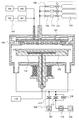
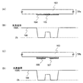
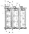
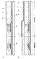
本実施の形態では、液晶表示装置に用いられる薄膜トランジスタの作製工程について、図1乃至図6を用いて説明する。図1乃至図3は、薄膜トランジスタの作製工程を示す断面図であり、図4は、一画素における薄膜トランジスタ及び画素電極の接続領域の上面図である。また、図5は、微結晶シリコン膜の成膜方法を示すタイミングチャートである。また、図6は、周波数の異なる二以上の高周波電力を供給してグロー放電プラズマを生成できるプラズマCVD装置の一構成例を示す断面図である。
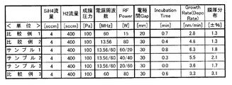
本形態は実施の形態1で示されるTFTを構成するゲート絶縁膜、微結晶半導体膜、n+層の成膜に適したマルチチャンバ方式のプラズマCVD装置の一例を示す。
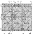
本実施の形態では、実施の形態2に示した図10と異なるマルチチャンバ方式のCVD装置を用いる薄膜トランジスタの作製工程について、図11を用いて説明する。図10は、3つの反応室を備えた装置であるのに対し、図11は、4つの反応室を備えたマルチチャンバ方式のCVD装置の上面図である。
実施の形態1とは異なる薄膜トランジスタの作製方法について、図12乃至図16を用いて説明する。ここでは、上記実施の形態1よりフォトマスク数を削減することが可能なプロセスを用いて薄膜トランジスタを作製する工程について示す。
本実施の形態では、表示装置の一形態として、実施の形態1で示す薄膜トランジスタを有する液晶表示装置について、以下に示す。
本実施の形態では、表示装置の一形態である発光装置について、図13乃至図15、図31、及び図32を用いて説明する。発光装置としては、ここではエレクトロルミネッセンスを利用する発光素子を用いて示す。エレクトロルミネッセンスを利用する発光素子は、発光材料が有機化合物であるか、無機化合物であるかによって区別され、一般的に、前者は有機EL素子、後者は無機EL素子と呼ばれている。
本発明の表示装置の一形態である表示パネルの構成について、以下に示す。
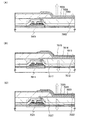
本発明の表示装置の一形態に相当する液晶表示パネルの外観及び断面について、図37を用いて説明する。図37(A)は、第1の基板4001上に形成された微結晶半導体膜を有する薄膜トランジスタ4010及び液晶素子4013を、第2の基板4006との間にシール材4005によって封止した、パネルの上面図であり、図37(B)は、図37(A)のA−A’における断面図相当する。
次に、本発明の表示装置の一形態に相当する発光表示パネルの外観及び断面について、図38を用いて説明する。図38(A)は、第1の基板上に形成された微結晶半導体膜を用いた薄膜トランジスタ及び発光素子を、第2の基板との間にシール材によって封止した、パネルの上面図であり、図38(B)は、図38(A)のA−A’における断面図に相当する。
本発明により得られる表示装置等によって、アクティブマトリクス型表示装置モジュールに用いることができる。即ち、それらを表示部に組み込んだ電子機器全てに本発明を実施できる。
12:駆動回路部
23:微結晶半導体膜
50:基板
51:ゲート電極
52a、52b、52c:ゲート絶縁膜
53:微結晶半導体膜
54:バッファ層
55:一導電型を付与する不純物が添加された半導体膜
56:レジストマスク
59:多階調マスク
61:微結晶半導体膜
62:バッファ層
63:一導電型を付与する不純物が添加された半導体膜
65a、65b、65c:導電膜
66:レジストマスク
71a、71b、71c:ソース電極及びドレイン電極
72:ソース領域及びドレイン領域
73:バッファ層
74:薄膜トランジスタ
76:絶縁膜
77:画素電極
80:レジストマスク
81:レジストマスク
83:薄膜トランジスタ
84:薄膜トランジスタ
85a〜85c導電膜
87:バッファ層
86:レジストマスク
88:ソース領域及びドレイン領域
90:微結晶半導体膜
91:隔壁
92a、92b、92c:ソース電極及びドレイン電極
93:平坦化膜
94:画素電極
95:発光層
96:共通電極
97:保護膜
98:発光素子
100a 第1反応室
100b 第2反応室
100c 第3反応室
100d 第4反応室
101 第1の電極
101a 第1の電極
101b 第1の電極
102 第2の電極
103 高周波電力供給手段
104 第1の高周波電源
105 第2の高周波電源
106 第1の整合器
107 第2の整合器
108 ガス供給手段
108g ガス供給手段
108i ガス供給手段
108n ガス供給手段
108a ガス供給手段
108f ガス供給手段
109 排気制御手段
110 シリンダ
111 圧力調整弁
112 ストップバルブ
113 マスフローコントローラ
114 基板加熱ヒータ
115 ヒータコントローラ
116 絶縁材
117 バタフライバルブ
118 コンダクタンスバルブ
119 ターボ分子ポンプ
120 ドライポンプ
121 クライオポンプ
122 ロード/アンロード室
123 共通室
124 カセット
125 ゲートバルブ
126 搬送機構
127 スイッチ
200 真空排気
201 プレコート
202 基板搬入
203 下地前処理
204 成膜処理
205 基板搬出
206 クリーニング
207 破線
Claims (4)
- 絶縁表面を有する基板上にゲート電極を形成し、
前記ゲート電極上に絶縁膜を成膜し、
前記基板を真空チャンバー内に導入し、
前記真空チャンバー内に材料ガスを導入し、
前記真空チャンバー内にグロー放電プラズマを生成する電極に、波長10m以上の周波数を有する第1の高周波電力と、波長10m未満の周波数を有する第2の高周波電力とを重畳印加してグロー放電プラズマを生成する第1の成膜条件により微結晶半導体膜の下部を成膜し、
前記第1の成膜条件と、基板温度、電力、周波数、前記材料ガスの流量、または真空度の少なくとも1つの条件が異なる第2の成膜条件で前記真空チャンバーと同一チャンバー内で前記微結晶半導体膜の上部を堆積し、
前記微結晶半導体膜上にバッファ層を成膜し、
前記第1の成膜条件は、前記第1の高周波電力と、前記第1の高周波電力よりも電力の大きい前記第2の高周波電力とを重畳印加し、
前記第2の成膜条件は、前記第1の高周波電力よりも大きい第3の高周波電力と、前記第3の高周波電力よりも電力の小さい第4の高周波電力を印加し、
前記第3の高周波電力の周波数は前記第1の高周波電力と同じであり、
前記第4の高周波電力の周波数は前記第2の高周波電力と同じである半導体装置の作製方法。 - 絶縁表面を有する基板上にゲート電極を形成し、
前記ゲート電極上に絶縁膜を成膜し、
前記基板を真空チャンバー内に導入し、
前記真空チャンバー内に材料ガスを導入し、
前記真空チャンバー内にグロー放電プラズマを生成する電極に、3MHz〜30MHzの第1の高周波電力と、30MHz〜300MHzの第2の高周波電力とを重畳印加してグロー放電プラズマを生成する第1の成膜条件により微結晶半導体膜の下部を成膜し、
前記第1の成膜条件と、基板温度、電力、周波数、前記材料ガスの流量、または真空度の少なくとも1つの条件が異なる第2の成膜条件で前記真空チャンバーと同一チャンバー内で前記微結晶半導体膜の上部を堆積し、
前記微結晶半導体膜上にバッファ層を成膜し、
前記第1の成膜条件は、前記第1の高周波電力と、前記第1の高周波電力よりも電力の大きい前記第2の高周波電力とを重畳印加し、
前記第2の成膜条件は、前記第1の高周波電力よりも大きい第3の高周波電力と、前記第3の高周波電力よりも電力の小さい第4の高周波電力を印加し、
前記第3の高周波電力の周波数は前記第1の高周波電力と同じであり、
前記第4の高周波電力の周波数は前記第2の高周波電力と同じである半導体装置の作製方法。 - 絶縁表面を有する基板上にゲート電極を形成し、
前記ゲート電極上に絶縁膜を成膜し、
前記基板を真空チャンバー内に導入し、
前記真空チャンバー内に材料ガスを導入し、
前記真空チャンバー内にグロー放電プラズマを生成する電極に、波長10m以上の周波数を有する第1の高周波電力と、波長10m未満の周波数を有する第2の高周波電力とを重畳印加してグロー放電プラズマを生成する第1の成膜条件により微結晶半導体膜の下部を成膜し、
前記第1の成膜条件と、基板温度、電力、周波数、前記材料ガスの流量、または真空度の少なくとも1つの条件が異なる第2の成膜条件で前記真空チャンバーと同一チャンバー内で前記微結晶半導体膜の上部を堆積し、
前記微結晶半導体膜上にバッファ層を成膜し、
前記第1の成膜条件は、前記第1の高周波電力と前記第2の高周波電力とを重畳印加し、
前記第2の成膜条件は、重畳印加することなく、前記第1の高周波電力と同じ周波数の第3の高周波電力を印加する半導体装置の作製方法。 - 絶縁表面を有する基板上にゲート電極を形成し、
前記ゲート電極上に絶縁膜を成膜し、
前記基板を真空チャンバー内に導入し、
前記真空チャンバー内に材料ガスを導入し、
前記真空チャンバー内にグロー放電プラズマを生成する電極に、3MHz〜30MHzの第1の高周波電力と、30MHz〜300MHzの第2の高周波電力とを重畳印加してグロー放電プラズマを生成する第1の成膜条件により微結晶半導体膜の下部を成膜し、
前記第1の成膜条件と、基板温度、電力、周波数、前記材料ガスの流量、または真空度の少なくとも1つの条件が異なる第2の成膜条件で前記真空チャンバーと同一チャンバー内で前記微結晶半導体膜の上部を堆積し、
前記微結晶半導体膜上にバッファ層を成膜し、
前記第1の成膜条件は、前記第1の高周波電力と前記第2の高周波電力とを重畳印加し、
前記第2の成膜条件は、重畳印加することなく、前記第1の高周波電力と同じ周波数の第3の高周波電力を印加する半導体装置の作製方法。
Priority Applications (1)
| Application Number | Priority Date | Filing Date | Title |
|---|---|---|---|
| JP2008204717A JP5331407B2 (ja) | 2007-08-17 | 2008-08-07 | 半導体装置の作製方法 |
Applications Claiming Priority (3)
| Application Number | Priority Date | Filing Date | Title |
|---|---|---|---|
| JP2007213102 | 2007-08-17 | ||
| JP2007213102 | 2007-08-17 | ||
| JP2008204717A JP5331407B2 (ja) | 2007-08-17 | 2008-08-07 | 半導体装置の作製方法 |
Publications (3)
| Publication Number | Publication Date |
|---|---|
| JP2009071291A JP2009071291A (ja) | 2009-04-02 |
| JP2009071291A5 JP2009071291A5 (ja) | 2011-08-11 |
| JP5331407B2 true JP5331407B2 (ja) | 2013-10-30 |
Family
ID=40363290
Family Applications (1)
| Application Number | Title | Priority Date | Filing Date |
|---|---|---|---|
| JP2008204717A Expired - Fee Related JP5331407B2 (ja) | 2007-08-17 | 2008-08-07 | 半導体装置の作製方法 |
Country Status (5)
| Country | Link |
|---|---|
| US (2) | US7833845B2 (ja) |
| JP (1) | JP5331407B2 (ja) |
| KR (1) | KR101518792B1 (ja) |
| CN (1) | CN101369540B (ja) |
| TW (1) | TWI447915B (ja) |
Cited By (1)
| Publication number | Priority date | Publication date | Assignee | Title |
|---|---|---|---|---|
| JP7210258B2 (ja) | 2018-12-10 | 2023-01-23 | Agcコーテック株式会社 | 塗料、タービンが有するブレード、航空機の翼 |
Families Citing this family (40)
| Publication number | Priority date | Publication date | Assignee | Title |
|---|---|---|---|---|
| US6825488B2 (en) * | 2000-01-26 | 2004-11-30 | Semiconductor Energy Laboratory Co., Ltd. | Semiconductor device and manufacturing method thereof |
| WO2009011084A1 (ja) * | 2007-07-17 | 2009-01-22 | Sharp Kabushiki Kaisha | 薄膜トランジスタを備えた半導体装置およびその製造方法 |
| JP5331407B2 (ja) * | 2007-08-17 | 2013-10-30 | 株式会社半導体エネルギー研究所 | 半導体装置の作製方法 |
| US8247315B2 (en) * | 2008-03-17 | 2012-08-21 | Semiconductor Energy Laboratory Co., Ltd. | Plasma processing apparatus and method for manufacturing semiconductor device |
| US7989325B2 (en) * | 2009-01-13 | 2011-08-02 | Semiconductor Energy Laboratory Co., Ltd. | Method for manufacturing crystalline semiconductor film and method for manufacturing thin film transistor |
| KR101291395B1 (ko) * | 2009-06-30 | 2013-07-30 | 가부시키가이샤 한도오따이 에네루기 켄큐쇼 | 반도체 장치 제조 방법 |
| KR101457837B1 (ko) | 2009-06-30 | 2014-11-05 | 가부시키가이샤 한도오따이 에네루기 켄큐쇼 | 반도체 장치 제작 방법 |
| EP2284891B1 (en) | 2009-08-07 | 2019-07-24 | Semiconductor Energy Laboratory Co, Ltd. | Semiconductor device and manufacturing method thereof |
| TWI634642B (zh) | 2009-08-07 | 2018-09-01 | 半導體能源研究所股份有限公司 | 半導體裝置和其製造方法 |
| JP5642447B2 (ja) * | 2009-08-07 | 2014-12-17 | 株式会社半導体エネルギー研究所 | 半導体装置 |
| KR102528026B1 (ko) | 2009-09-04 | 2023-05-03 | 가부시키가이샤 한도오따이 에네루기 켄큐쇼 | 발광 장치 및 발광 장치를 제작하기 위한 방법 |
| CN104934483B (zh) * | 2009-09-24 | 2018-08-10 | 株式会社半导体能源研究所 | 半导体元件及其制造方法 |
| KR20120084751A (ko) | 2009-10-05 | 2012-07-30 | 가부시키가이샤 한도오따이 에네루기 켄큐쇼 | 반도체 장치 및 그 제작 방법 |
| WO2011052384A1 (en) | 2009-10-30 | 2011-05-05 | Semiconductor Energy Laboratory Co., Ltd. | Semiconductor device and method for manufacturing the same |
| JP5508889B2 (ja) * | 2010-02-16 | 2014-06-04 | 日本放送協会 | 薄膜蛍光体、ディスプレイ、ブラウン管および薄膜蛍光体の製造方法 |
| US8383434B2 (en) * | 2010-02-22 | 2013-02-26 | Semiconductor Energy Laboratory Co., Ltd. | Thin film transistor and manufacturing method thereof |
| JP5785770B2 (ja) | 2010-05-14 | 2015-09-30 | 株式会社半導体エネルギー研究所 | 微結晶半導体膜の作製方法、及び半導体装置の作製方法 |
| US8884297B2 (en) | 2010-05-14 | 2014-11-11 | Semiconductor Energy Laboratory Co., Ltd. | Microcrystalline silicon film, manufacturing method thereof, semiconductor device, and manufacturing method thereof |
| US8778745B2 (en) | 2010-06-29 | 2014-07-15 | Semiconductor Energy Laboratory Co., Ltd. | Method for manufacturing semiconductor device |
| US9170424B2 (en) * | 2010-07-30 | 2015-10-27 | Sony Corporation | Illumination unit and display |
| CN102386072B (zh) | 2010-08-25 | 2016-05-04 | 株式会社半导体能源研究所 | 微晶半导体膜的制造方法及半导体装置的制造方法 |
| US8338240B2 (en) * | 2010-10-01 | 2012-12-25 | Semiconductor Energy Laboratory Co., Ltd. | Method for manufacturing transistor |
| JP2012089708A (ja) | 2010-10-20 | 2012-05-10 | Semiconductor Energy Lab Co Ltd | 微結晶シリコン膜の作製方法、半導体装置の作製方法 |
| US8450158B2 (en) | 2010-11-04 | 2013-05-28 | Semiconductor Energy Laboratory Co., Ltd. | Method for forming microcrystalline semiconductor film and method for manufacturing semiconductor device |
| US8394685B2 (en) | 2010-12-06 | 2013-03-12 | Semiconductor Energy Laboratory Co., Ltd. | Etching method and manufacturing method of thin film transistor |
| KR101770969B1 (ko) * | 2011-01-21 | 2017-08-25 | 삼성디스플레이 주식회사 | 터치 센싱 기판 및 이의 제조 방법 |
| US9048327B2 (en) | 2011-01-25 | 2015-06-02 | Semiconductor Energy Laboratory Co., Ltd. | Microcrystalline semiconductor film, method for manufacturing the same, and method for manufacturing semiconductor device |
| JP2013051370A (ja) * | 2011-08-31 | 2013-03-14 | Tokyo Electron Ltd | 成膜方法及び記憶媒体 |
| WO2013118462A1 (ja) * | 2012-02-06 | 2013-08-15 | パナソニック株式会社 | El表示装置およびその製造方法 |
| JP5963564B2 (ja) | 2012-06-20 | 2016-08-03 | スタンレー電気株式会社 | 液晶表示装置 |
| JP2014107447A (ja) * | 2012-11-28 | 2014-06-09 | Nitto Denko Corp | 封止シート、光半導体装置およびその製造方法 |
| KR20140090019A (ko) * | 2013-01-08 | 2014-07-16 | 삼성디스플레이 주식회사 | 표시 장치 |
| JP6219227B2 (ja) * | 2014-05-12 | 2017-10-25 | 東京エレクトロン株式会社 | ヒータ給電機構及びステージの温度制御方法 |
| JP6219229B2 (ja) * | 2014-05-19 | 2017-10-25 | 東京エレクトロン株式会社 | ヒータ給電機構 |
| US20160155803A1 (en) * | 2014-11-28 | 2016-06-02 | Semiconductor Energy Laboratory Co., Ltd. | Semiconductor Device, Method for Manufacturing the Semiconductor Device, and Display Device Including the Semiconductor Device |
| CN104532192B (zh) * | 2014-12-19 | 2018-01-30 | 深圳市华星光电技术有限公司 | 蒸镀装置 |
| KR102440302B1 (ko) | 2015-04-13 | 2022-09-05 | 가부시키가이샤 한도오따이 에네루기 켄큐쇼 | 반도체 장치 및 그 제작 방법 |
| WO2018225183A1 (ja) * | 2017-06-07 | 2018-12-13 | シャープ株式会社 | 表示デバイス、表示デバイスの製造方法、表示デバイスの製造装置 |
| US10950416B2 (en) * | 2018-11-16 | 2021-03-16 | Mattson Technology, Inc. | Chamber seasoning to improve etch uniformity by reducing chemistry |
| CN113394235B (zh) * | 2021-05-20 | 2022-10-21 | 北海惠科光电技术有限公司 | 阵列基板及阵列基板的制造方法 |
Family Cites Families (16)
| Publication number | Priority date | Publication date | Assignee | Title |
|---|---|---|---|---|
| AU530905B2 (en) * | 1977-12-22 | 1983-08-04 | Canon Kabushiki Kaisha | Electrophotographic photosensitive member |
| US4605941A (en) * | 1978-03-08 | 1986-08-12 | Energy Conversion Devices, Inc. | Amorphous semiconductors equivalent to crystalline semiconductors |
| US5091334A (en) | 1980-03-03 | 1992-02-25 | Semiconductor Energy Laboratory Co., Ltd. | Semiconductor device |
| JPS56122123A (en) * | 1980-03-03 | 1981-09-25 | Shunpei Yamazaki | Semiamorphous semiconductor |
| JP2726414B2 (ja) * | 1987-03-04 | 1998-03-11 | 株式会社東芝 | ケイ素系薄膜の製造方法 |
| JPH06326026A (ja) | 1993-04-13 | 1994-11-25 | Applied Materials Inc | 半導体装置の薄膜形成方法 |
| US5571571A (en) | 1993-06-16 | 1996-11-05 | Applied Materials, Inc. | Method of forming a thin film for a semiconductor device |
| JPH0794749A (ja) * | 1993-09-22 | 1995-04-07 | Toshiba Corp | 薄膜トランジスタの製造方法 |
| JP3376051B2 (ja) * | 1993-12-03 | 2003-02-10 | 三菱電機株式会社 | 薄膜トランジスタおよびその製造方法 |
| KR100241817B1 (ko) * | 1993-12-27 | 2000-02-01 | 니시무로 타이죠 | 박막형성법 |
| JPH07254592A (ja) | 1994-03-16 | 1995-10-03 | Fujitsu Ltd | 半導体装置の製造方法 |
| JPH0888397A (ja) * | 1994-09-16 | 1996-04-02 | Casio Comput Co Ltd | 光電変換素子 |
| TW303526B (ja) * | 1994-12-27 | 1997-04-21 | Matsushita Electric Ind Co Ltd | |
| JPH09232235A (ja) * | 1995-02-24 | 1997-09-05 | Mitsui Toatsu Chem Inc | 光電変換素子 |
| JP3897582B2 (ja) * | 2000-12-12 | 2007-03-28 | キヤノン株式会社 | 真空処理方法、真空処理装置、半導体装置の製造方法および半導体装置 |
| JP5331407B2 (ja) * | 2007-08-17 | 2013-10-30 | 株式会社半導体エネルギー研究所 | 半導体装置の作製方法 |
-
2008
- 2008-08-07 JP JP2008204717A patent/JP5331407B2/ja not_active Expired - Fee Related
- 2008-08-12 TW TW097130670A patent/TWI447915B/zh not_active IP Right Cessation
- 2008-08-12 US US12/222,547 patent/US7833845B2/en not_active Expired - Fee Related
- 2008-08-14 CN CN2008102104921A patent/CN101369540B/zh not_active Expired - Fee Related
- 2008-08-14 KR KR1020080080030A patent/KR101518792B1/ko not_active IP Right Cessation
-
2010
- 2010-11-12 US US12/944,841 patent/US8263421B2/en not_active Expired - Fee Related
Cited By (1)
| Publication number | Priority date | Publication date | Assignee | Title |
|---|---|---|---|---|
| JP7210258B2 (ja) | 2018-12-10 | 2023-01-23 | Agcコーテック株式会社 | 塗料、タービンが有するブレード、航空機の翼 |
Also Published As
| Publication number | Publication date |
|---|---|
| CN101369540B (zh) | 2012-07-04 |
| US20090047761A1 (en) | 2009-02-19 |
| US8263421B2 (en) | 2012-09-11 |
| US7833845B2 (en) | 2010-11-16 |
| JP2009071291A (ja) | 2009-04-02 |
| US20110059562A1 (en) | 2011-03-10 |
| TWI447915B (zh) | 2014-08-01 |
| KR101518792B1 (ko) | 2015-05-12 |
| KR20090018587A (ko) | 2009-02-20 |
| CN101369540A (zh) | 2009-02-18 |
| TW200917493A (en) | 2009-04-16 |
Similar Documents
| Publication | Publication Date | Title |
|---|---|---|
| JP5331407B2 (ja) | 半導体装置の作製方法 | |
| JP7290769B2 (ja) | 半導体装置 | |
| JP7432052B2 (ja) | 表示装置 | |
| JP6154880B2 (ja) | 表示装置の作製方法 | |
| US9054206B2 (en) | Method for manufacturing semiconductor device | |
| US8253138B2 (en) | Thin film transistor and display device having the thin film transistor | |
| US8951849B2 (en) | Method for manufacturing semiconductor device including layer containing yttria-stabilized zirconia | |
| US8633485B2 (en) | Display device and manufacturing method thereof | |
| JP5503857B2 (ja) | 薄膜トランジスタの作製方法 | |
| JP2009130229A (ja) | 半導体装置の作製方法 | |
| JP2016170417A (ja) | 半導体装置 | |
| JP5314870B2 (ja) | 薄膜トランジスタの作製方法 | |
| JP2009071288A (ja) | 半導体装置の作製方法 | |
| JP5496500B2 (ja) | 半導体装置の作製方法 | |
| JP5297629B2 (ja) | 半導体装置の作製方法 |
Legal Events
| Date | Code | Title | Description |
|---|---|---|---|
| A521 | Request for written amendment filed |
Free format text: JAPANESE INTERMEDIATE CODE: A523 Effective date: 20110628 |
|
| A621 | Written request for application examination |
Free format text: JAPANESE INTERMEDIATE CODE: A621 Effective date: 20110628 |
|
| A977 | Report on retrieval |
Free format text: JAPANESE INTERMEDIATE CODE: A971007 Effective date: 20130509 |
|
| A131 | Notification of reasons for refusal |
Free format text: JAPANESE INTERMEDIATE CODE: A131 Effective date: 20130514 |
|
| A521 | Request for written amendment filed |
Free format text: JAPANESE INTERMEDIATE CODE: A523 Effective date: 20130531 |
|
| TRDD | Decision of grant or rejection written | ||
| A01 | Written decision to grant a patent or to grant a registration (utility model) |
Free format text: JAPANESE INTERMEDIATE CODE: A01 Effective date: 20130723 |
|
| A61 | First payment of annual fees (during grant procedure) |
Free format text: JAPANESE INTERMEDIATE CODE: A61 Effective date: 20130729 |
|
| R150 | Certificate of patent or registration of utility model |
Ref document number: 5331407 Country of ref document: JP Free format text: JAPANESE INTERMEDIATE CODE: R150 Free format text: JAPANESE INTERMEDIATE CODE: R150 |
|
| R250 | Receipt of annual fees |
Free format text: JAPANESE INTERMEDIATE CODE: R250 |
|
| R250 | Receipt of annual fees |
Free format text: JAPANESE INTERMEDIATE CODE: R250 |
|
| R250 | Receipt of annual fees |
Free format text: JAPANESE INTERMEDIATE CODE: R250 |
|
| LAPS | Cancellation because of no payment of annual fees |