JP5331407B2 - Method for manufacturing semiconductor device - Google Patents
Method for manufacturing semiconductor device Download PDFInfo
- Publication number
- JP5331407B2 JP5331407B2 JP2008204717A JP2008204717A JP5331407B2 JP 5331407 B2 JP5331407 B2 JP 5331407B2 JP 2008204717 A JP2008204717 A JP 2008204717A JP 2008204717 A JP2008204717 A JP 2008204717A JP 5331407 B2 JP5331407 B2 JP 5331407B2
- Authority
- JP
- Japan
- Prior art keywords
- film
- frequency power
- substrate
- semiconductor film
- frequency
- Prior art date
- Legal status (The legal status is an assumption and is not a legal conclusion. Google has not performed a legal analysis and makes no representation as to the accuracy of the status listed.)
- Expired - Fee Related
Links
- 239000004065 semiconductor Substances 0.000 title claims abstract description 242
- 238000004519 manufacturing process Methods 0.000 title claims abstract description 41
- 238000000034 method Methods 0.000 title claims description 70
- 239000000758 substrate Substances 0.000 claims abstract description 199
- 230000015572 biosynthetic process Effects 0.000 claims abstract description 168
- 239000000463 material Substances 0.000 claims description 36
- 230000008021 deposition Effects 0.000 claims description 25
- 239000013081 microcrystal Substances 0.000 claims description 11
- 230000002349 favourable effect Effects 0.000 abstract 1
- 239000010408 film Substances 0.000 description 710
- 239000010410 layer Substances 0.000 description 174
- 238000005755 formation reaction Methods 0.000 description 164
- 239000010409 thin film Substances 0.000 description 119
- 239000004973 liquid crystal related substance Substances 0.000 description 104
- 239000007789 gas Substances 0.000 description 84
- 238000006243 chemical reaction Methods 0.000 description 75
- 229910021424 microcrystalline silicon Inorganic materials 0.000 description 58
- 239000012535 impurity Substances 0.000 description 53
- 230000001965 increasing effect Effects 0.000 description 43
- 230000008569 process Effects 0.000 description 31
- 239000001257 hydrogen Substances 0.000 description 30
- 229910052739 hydrogen Inorganic materials 0.000 description 30
- QVGXLLKOCUKJST-UHFFFAOYSA-N atomic oxygen Chemical compound [O] QVGXLLKOCUKJST-UHFFFAOYSA-N 0.000 description 29
- 239000001301 oxygen Substances 0.000 description 29
- 229910052760 oxygen Inorganic materials 0.000 description 29
- BLRPTPMANUNPDV-UHFFFAOYSA-N Silane Chemical compound [SiH4] BLRPTPMANUNPDV-UHFFFAOYSA-N 0.000 description 28
- UFHFLCQGNIYNRP-UHFFFAOYSA-N Hydrogen Chemical compound [H][H] UFHFLCQGNIYNRP-UHFFFAOYSA-N 0.000 description 27
- 239000011521 glass Substances 0.000 description 25
- IJGRMHOSHXDMSA-UHFFFAOYSA-N Atomic nitrogen Chemical compound N#N IJGRMHOSHXDMSA-UHFFFAOYSA-N 0.000 description 24
- 238000000151 deposition Methods 0.000 description 23
- 238000005268 plasma chemical vapour deposition Methods 0.000 description 22
- 229910021417 amorphous silicon Inorganic materials 0.000 description 20
- 230000005684 electric field Effects 0.000 description 19
- 238000005530 etching Methods 0.000 description 19
- 229910052782 aluminium Inorganic materials 0.000 description 18
- XAGFODPZIPBFFR-UHFFFAOYSA-N aluminium Chemical compound [Al] XAGFODPZIPBFFR-UHFFFAOYSA-N 0.000 description 18
- 239000003990 capacitor Substances 0.000 description 18
- 238000011534 incubation Methods 0.000 description 18
- 229910000077 silane Inorganic materials 0.000 description 17
- 229910052581 Si3N4 Inorganic materials 0.000 description 16
- 229910052710 silicon Inorganic materials 0.000 description 16
- HQVNEWCFYHHQES-UHFFFAOYSA-N silicon nitride Chemical compound N12[Si]34N5[Si]62N3[Si]51N64 HQVNEWCFYHHQES-UHFFFAOYSA-N 0.000 description 16
- XUIMIQQOPSSXEZ-UHFFFAOYSA-N Silicon Chemical compound [Si] XUIMIQQOPSSXEZ-UHFFFAOYSA-N 0.000 description 15
- 239000010703 silicon Substances 0.000 description 15
- XKRFYHLGVUSROY-UHFFFAOYSA-N Argon Chemical compound [Ar] XKRFYHLGVUSROY-UHFFFAOYSA-N 0.000 description 14
- 230000001976 improved effect Effects 0.000 description 14
- 239000013078 crystal Substances 0.000 description 13
- 230000006870 function Effects 0.000 description 13
- AMGQUBHHOARCQH-UHFFFAOYSA-N indium;oxotin Chemical compound [In].[Sn]=O AMGQUBHHOARCQH-UHFFFAOYSA-N 0.000 description 13
- 229910052751 metal Inorganic materials 0.000 description 13
- 229910052757 nitrogen Inorganic materials 0.000 description 12
- 230000001276 controlling effect Effects 0.000 description 11
- 238000010438 heat treatment Methods 0.000 description 11
- 239000002184 metal Substances 0.000 description 11
- 238000009832 plasma treatment Methods 0.000 description 11
- 229910052990 silicon hydride Inorganic materials 0.000 description 11
- 125000006850 spacer group Chemical group 0.000 description 9
- 238000002834 transmittance Methods 0.000 description 9
- ZOKXTWBITQBERF-UHFFFAOYSA-N Molybdenum Chemical compound [Mo] ZOKXTWBITQBERF-UHFFFAOYSA-N 0.000 description 8
- 239000012298 atmosphere Substances 0.000 description 8
- 239000002585 base Substances 0.000 description 8
- 239000000460 chlorine Substances 0.000 description 8
- 238000004140 cleaning Methods 0.000 description 8
- 230000005669 field effect Effects 0.000 description 8
- 229910052750 molybdenum Inorganic materials 0.000 description 8
- 239000011733 molybdenum Substances 0.000 description 8
- 239000000565 sealant Substances 0.000 description 8
- 238000003860 storage Methods 0.000 description 8
- 229910052786 argon Inorganic materials 0.000 description 7
- 239000004020 conductor Substances 0.000 description 7
- 238000005192 partition Methods 0.000 description 7
- 229920005989 resin Polymers 0.000 description 7
- 239000011347 resin Substances 0.000 description 7
- 239000002356 single layer Substances 0.000 description 7
- 238000004544 sputter deposition Methods 0.000 description 7
- VYPSYNLAJGMNEJ-UHFFFAOYSA-N Silicium dioxide Chemical compound O=[Si]=O VYPSYNLAJGMNEJ-UHFFFAOYSA-N 0.000 description 6
- RTAQQCXQSZGOHL-UHFFFAOYSA-N Titanium Chemical compound [Ti] RTAQQCXQSZGOHL-UHFFFAOYSA-N 0.000 description 6
- 239000011248 coating agent Substances 0.000 description 6
- 238000000576 coating method Methods 0.000 description 6
- 238000004040 coloring Methods 0.000 description 6
- 238000010586 diagram Methods 0.000 description 6
- 230000000694 effects Effects 0.000 description 6
- 239000000203 mixture Substances 0.000 description 6
- 239000012495 reaction gas Substances 0.000 description 6
- 229910052719 titanium Inorganic materials 0.000 description 6
- 239000010936 titanium Substances 0.000 description 6
- 229910000838 Al alloy Inorganic materials 0.000 description 5
- RYGMFSIKBFXOCR-UHFFFAOYSA-N Copper Chemical compound [Cu] RYGMFSIKBFXOCR-UHFFFAOYSA-N 0.000 description 5
- 230000000052 comparative effect Effects 0.000 description 5
- 229910052802 copper Inorganic materials 0.000 description 5
- 239000010949 copper Substances 0.000 description 5
- 239000001307 helium Substances 0.000 description 5
- 229910052734 helium Inorganic materials 0.000 description 5
- SWQJXJOGLNCZEY-UHFFFAOYSA-N helium atom Chemical compound [He] SWQJXJOGLNCZEY-UHFFFAOYSA-N 0.000 description 5
- -1 moisture Substances 0.000 description 5
- 230000010355 oscillation Effects 0.000 description 5
- 239000000843 powder Substances 0.000 description 5
- 230000001681 protective effect Effects 0.000 description 5
- 229910052814 silicon oxide Inorganic materials 0.000 description 5
- ZCYVEMRRCGMTRW-UHFFFAOYSA-N 7553-56-2 Chemical compound [I] ZCYVEMRRCGMTRW-UHFFFAOYSA-N 0.000 description 4
- QGZKDVFQNNGYKY-UHFFFAOYSA-N Ammonia Chemical compound N QGZKDVFQNNGYKY-UHFFFAOYSA-N 0.000 description 4
- WKBOTKDWSSQWDR-UHFFFAOYSA-N Bromine atom Chemical compound [Br] WKBOTKDWSSQWDR-UHFFFAOYSA-N 0.000 description 4
- ZAMOUSCENKQFHK-UHFFFAOYSA-N Chlorine atom Chemical compound [Cl] ZAMOUSCENKQFHK-UHFFFAOYSA-N 0.000 description 4
- PXGOKWXKJXAPGV-UHFFFAOYSA-N Fluorine Chemical compound FF PXGOKWXKJXAPGV-UHFFFAOYSA-N 0.000 description 4
- GWEVSGVZZGPLCZ-UHFFFAOYSA-N Titan oxide Chemical compound O=[Ti]=O GWEVSGVZZGPLCZ-UHFFFAOYSA-N 0.000 description 4
- GDTBXPJZTBHREO-UHFFFAOYSA-N bromine Substances BrBr GDTBXPJZTBHREO-UHFFFAOYSA-N 0.000 description 4
- 229910052794 bromium Inorganic materials 0.000 description 4
- 229910052801 chlorine Inorganic materials 0.000 description 4
- 229920001940 conductive polymer Polymers 0.000 description 4
- 238000005520 cutting process Methods 0.000 description 4
- 230000003247 decreasing effect Effects 0.000 description 4
- 239000011737 fluorine Substances 0.000 description 4
- 229910052731 fluorine Inorganic materials 0.000 description 4
- 150000002431 hydrogen Chemical class 0.000 description 4
- 229910003437 indium oxide Inorganic materials 0.000 description 4
- PJXISJQVUVHSOJ-UHFFFAOYSA-N indium(iii) oxide Chemical compound [O-2].[O-2].[O-2].[In+3].[In+3] PJXISJQVUVHSOJ-UHFFFAOYSA-N 0.000 description 4
- 238000003780 insertion Methods 0.000 description 4
- 230000037431 insertion Effects 0.000 description 4
- 239000011630 iodine Substances 0.000 description 4
- 229910052740 iodine Inorganic materials 0.000 description 4
- QGLKJKCYBOYXKC-UHFFFAOYSA-N nonaoxidotritungsten Chemical compound O=[W]1(=O)O[W](=O)(=O)O[W](=O)(=O)O1 QGLKJKCYBOYXKC-UHFFFAOYSA-N 0.000 description 4
- 238000012545 processing Methods 0.000 description 4
- 230000005236 sound signal Effects 0.000 description 4
- OGIDPMRJRNCKJF-UHFFFAOYSA-N titanium oxide Inorganic materials [Ti]=O OGIDPMRJRNCKJF-UHFFFAOYSA-N 0.000 description 4
- 229910001930 tungsten oxide Inorganic materials 0.000 description 4
- YVTHLONGBIQYBO-UHFFFAOYSA-N zinc indium(3+) oxygen(2-) Chemical compound [O--].[Zn++].[In+3] YVTHLONGBIQYBO-UHFFFAOYSA-N 0.000 description 4
- VYZAMTAEIAYCRO-UHFFFAOYSA-N Chromium Chemical compound [Cr] VYZAMTAEIAYCRO-UHFFFAOYSA-N 0.000 description 3
- NIXOWILDQLNWCW-UHFFFAOYSA-N acrylic acid group Chemical group C(C=C)(=O)O NIXOWILDQLNWCW-UHFFFAOYSA-N 0.000 description 3
- 238000000137 annealing Methods 0.000 description 3
- 239000000969 carrier Substances 0.000 description 3
- 230000008859 change Effects 0.000 description 3
- 229910052804 chromium Inorganic materials 0.000 description 3
- 239000011651 chromium Substances 0.000 description 3
- 230000006866 deterioration Effects 0.000 description 3
- 239000000945 filler Substances 0.000 description 3
- 239000011810 insulating material Substances 0.000 description 3
- 229910052743 krypton Inorganic materials 0.000 description 3
- DNNSSWSSYDEUBZ-UHFFFAOYSA-N krypton atom Chemical compound [Kr] DNNSSWSSYDEUBZ-UHFFFAOYSA-N 0.000 description 3
- 230000007246 mechanism Effects 0.000 description 3
- 150000004767 nitrides Chemical class 0.000 description 3
- 150000002894 organic compounds Chemical class 0.000 description 3
- 230000003647 oxidation Effects 0.000 description 3
- 238000007254 oxidation reaction Methods 0.000 description 3
- 238000000206 photolithography Methods 0.000 description 3
- 229920003023 plastic Polymers 0.000 description 3
- 239000004033 plastic Substances 0.000 description 3
- 229920006267 polyester film Polymers 0.000 description 3
- 229920002620 polyvinyl fluoride Polymers 0.000 description 3
- 239000011148 porous material Substances 0.000 description 3
- 230000000630 rising effect Effects 0.000 description 3
- 229910052715 tantalum Inorganic materials 0.000 description 3
- GUVRBAGPIYLISA-UHFFFAOYSA-N tantalum atom Chemical compound [Ta] GUVRBAGPIYLISA-UHFFFAOYSA-N 0.000 description 3
- WFKWXMTUELFFGS-UHFFFAOYSA-N tungsten Chemical compound [W] WFKWXMTUELFFGS-UHFFFAOYSA-N 0.000 description 3
- 229910052721 tungsten Inorganic materials 0.000 description 3
- 239000010937 tungsten Substances 0.000 description 3
- 229910001316 Ag alloy Inorganic materials 0.000 description 2
- ZOXJGFHDIHLPTG-UHFFFAOYSA-N Boron Chemical compound [B] ZOXJGFHDIHLPTG-UHFFFAOYSA-N 0.000 description 2
- OYPRJOBELJOOCE-UHFFFAOYSA-N Calcium Chemical compound [Ca] OYPRJOBELJOOCE-UHFFFAOYSA-N 0.000 description 2
- OKTJSMMVPCPJKN-UHFFFAOYSA-N Carbon Chemical compound [C] OKTJSMMVPCPJKN-UHFFFAOYSA-N 0.000 description 2
- CURLTUGMZLYLDI-UHFFFAOYSA-N Carbon dioxide Chemical compound O=C=O CURLTUGMZLYLDI-UHFFFAOYSA-N 0.000 description 2
- VEXZGXHMUGYJMC-UHFFFAOYSA-N Hydrochloric acid Chemical compound Cl VEXZGXHMUGYJMC-UHFFFAOYSA-N 0.000 description 2
- OAICVXFJPJFONN-UHFFFAOYSA-N Phosphorus Chemical compound [P] OAICVXFJPJFONN-UHFFFAOYSA-N 0.000 description 2
- 239000004642 Polyimide Substances 0.000 description 2
- 238000001237 Raman spectrum Methods 0.000 description 2
- 229910003902 SiCl 4 Inorganic materials 0.000 description 2
- NRTOMJZYCJJWKI-UHFFFAOYSA-N Titanium nitride Chemical compound [Ti]#N NRTOMJZYCJJWKI-UHFFFAOYSA-N 0.000 description 2
- WGLPBDUCMAPZCE-UHFFFAOYSA-N Trioxochromium Chemical compound O=[Cr](=O)=O WGLPBDUCMAPZCE-UHFFFAOYSA-N 0.000 description 2
- 206010047571 Visual impairment Diseases 0.000 description 2
- JFBZPFYRPYOZCQ-UHFFFAOYSA-N [Li].[Al] Chemical compound [Li].[Al] JFBZPFYRPYOZCQ-UHFFFAOYSA-N 0.000 description 2
- 229910021529 ammonia Inorganic materials 0.000 description 2
- 230000003321 amplification Effects 0.000 description 2
- 125000004429 atom Chemical group 0.000 description 2
- 230000004888 barrier function Effects 0.000 description 2
- 229910052796 boron Inorganic materials 0.000 description 2
- DQXBYHZEEUGOBF-UHFFFAOYSA-N but-3-enoic acid;ethene Chemical compound C=C.OC(=O)CC=C DQXBYHZEEUGOBF-UHFFFAOYSA-N 0.000 description 2
- 229910052791 calcium Inorganic materials 0.000 description 2
- 239000011575 calcium Substances 0.000 description 2
- WUKWITHWXAAZEY-UHFFFAOYSA-L calcium difluoride Chemical compound [F-].[F-].[Ca+2] WUKWITHWXAAZEY-UHFFFAOYSA-L 0.000 description 2
- 229910001634 calcium fluoride Inorganic materials 0.000 description 2
- 229910052799 carbon Inorganic materials 0.000 description 2
- 238000005229 chemical vapour deposition Methods 0.000 description 2
- SLLGVCUQYRMELA-UHFFFAOYSA-N chlorosilicon Chemical compound Cl[Si] SLLGVCUQYRMELA-UHFFFAOYSA-N 0.000 description 2
- 229910000423 chromium oxide Inorganic materials 0.000 description 2
- 238000004891 communication Methods 0.000 description 2
- 239000000356 contaminant Substances 0.000 description 2
- 238000011109 contamination Methods 0.000 description 2
- 230000008878 coupling Effects 0.000 description 2
- 238000010168 coupling process Methods 0.000 description 2
- 238000005859 coupling reaction Methods 0.000 description 2
- 238000002425 crystallisation Methods 0.000 description 2
- 230000008025 crystallization Effects 0.000 description 2
- 230000007423 decrease Effects 0.000 description 2
- 230000007547 defect Effects 0.000 description 2
- 238000013461 design Methods 0.000 description 2
- 238000011161 development Methods 0.000 description 2
- 238000009792 diffusion process Methods 0.000 description 2
- 208000037265 diseases, disorders, signs and symptoms Diseases 0.000 description 2
- 238000009826 distribution Methods 0.000 description 2
- 238000001312 dry etching Methods 0.000 description 2
- 238000005401 electroluminescence Methods 0.000 description 2
- 239000005038 ethylene vinyl acetate Substances 0.000 description 2
- 230000005281 excited state Effects 0.000 description 2
- 239000000284 extract Substances 0.000 description 2
- 239000011152 fibreglass Substances 0.000 description 2
- 238000007667 floating Methods 0.000 description 2
- 229910052736 halogen Inorganic materials 0.000 description 2
- 150000002367 halogens Chemical class 0.000 description 2
- 230000006872 improvement Effects 0.000 description 2
- 238000002347 injection Methods 0.000 description 2
- 239000007924 injection Substances 0.000 description 2
- 230000001678 irradiating effect Effects 0.000 description 2
- 230000033001 locomotion Effects 0.000 description 2
- SJCKRGFTWFGHGZ-UHFFFAOYSA-N magnesium silver Chemical compound [Mg].[Ag] SJCKRGFTWFGHGZ-UHFFFAOYSA-N 0.000 description 2
- 239000011159 matrix material Substances 0.000 description 2
- 239000007769 metal material Substances 0.000 description 2
- 229910021421 monocrystalline silicon Inorganic materials 0.000 description 2
- 229910052754 neon Inorganic materials 0.000 description 2
- GKAOGPIIYCISHV-UHFFFAOYSA-N neon atom Chemical compound [Ne] GKAOGPIIYCISHV-UHFFFAOYSA-N 0.000 description 2
- 238000003199 nucleic acid amplification method Methods 0.000 description 2
- 239000002245 particle Substances 0.000 description 2
- 229910052698 phosphorus Inorganic materials 0.000 description 2
- 239000011574 phosphorus Substances 0.000 description 2
- 229920001200 poly(ethylene-vinyl acetate) Polymers 0.000 description 2
- 229920002037 poly(vinyl butyral) polymer Polymers 0.000 description 2
- 229920001721 polyimide Polymers 0.000 description 2
- 229920000915 polyvinyl chloride Polymers 0.000 description 2
- 239000004800 polyvinyl chloride Substances 0.000 description 2
- 230000009467 reduction Effects 0.000 description 2
- 239000010935 stainless steel Substances 0.000 description 2
- 229910001220 stainless steel Inorganic materials 0.000 description 2
- 239000000126 substance Substances 0.000 description 2
- 230000003746 surface roughness Effects 0.000 description 2
- 238000012360 testing method Methods 0.000 description 2
- 230000007723 transport mechanism Effects 0.000 description 2
- WXRGABKACDFXMG-UHFFFAOYSA-N trimethylborane Chemical compound CB(C)C WXRGABKACDFXMG-UHFFFAOYSA-N 0.000 description 2
- 238000001771 vacuum deposition Methods 0.000 description 2
- XLYOFNOQVPJJNP-UHFFFAOYSA-N water Substances O XLYOFNOQVPJJNP-UHFFFAOYSA-N 0.000 description 2
- 239000004925 Acrylic resin Substances 0.000 description 1
- 229920000178 Acrylic resin Polymers 0.000 description 1
- 229910019974 CrSi Inorganic materials 0.000 description 1
- 206010052128 Glare Diseases 0.000 description 1
- 244000126211 Hericium coralloides Species 0.000 description 1
- 229910016006 MoSi Inorganic materials 0.000 description 1
- 229910052779 Neodymium Inorganic materials 0.000 description 1
- 238000006124 Pilkington process Methods 0.000 description 1
- 239000004952 Polyamide Substances 0.000 description 1
- BQCADISMDOOEFD-UHFFFAOYSA-N Silver Chemical compound [Ag] BQCADISMDOOEFD-UHFFFAOYSA-N 0.000 description 1
- 230000002159 abnormal effect Effects 0.000 description 1
- 230000009471 action Effects 0.000 description 1
- 229910052783 alkali metal Inorganic materials 0.000 description 1
- 150000001340 alkali metals Chemical class 0.000 description 1
- 239000000956 alloy Substances 0.000 description 1
- 239000005407 aluminoborosilicate glass Substances 0.000 description 1
- 239000005354 aluminosilicate glass Substances 0.000 description 1
- 229910052788 barium Inorganic materials 0.000 description 1
- DSAJWYNOEDNPEQ-UHFFFAOYSA-N barium atom Chemical compound [Ba] DSAJWYNOEDNPEQ-UHFFFAOYSA-N 0.000 description 1
- 239000011324 bead Substances 0.000 description 1
- 230000008901 benefit Effects 0.000 description 1
- 239000011230 binding agent Substances 0.000 description 1
- 239000005388 borosilicate glass Substances 0.000 description 1
- 239000006227 byproduct Substances 0.000 description 1
- 229910002092 carbon dioxide Inorganic materials 0.000 description 1
- 239000001569 carbon dioxide Substances 0.000 description 1
- 230000015556 catabolic process Effects 0.000 description 1
- 230000001413 cellular effect Effects 0.000 description 1
- 239000000919 ceramic Substances 0.000 description 1
- 238000006757 chemical reactions by type Methods 0.000 description 1
- 238000007796 conventional method Methods 0.000 description 1
- 229920001577 copolymer Polymers 0.000 description 1
- 238000007872 degassing Methods 0.000 description 1
- 238000006356 dehydrogenation reaction Methods 0.000 description 1
- 238000007865 diluting Methods 0.000 description 1
- 238000010790 dilution Methods 0.000 description 1
- 239000012895 dilution Substances 0.000 description 1
- 238000007599 discharging Methods 0.000 description 1
- KPUWHANPEXNPJT-UHFFFAOYSA-N disiloxane Chemical class [SiH3]O[SiH3] KPUWHANPEXNPJT-UHFFFAOYSA-N 0.000 description 1
- 230000009977 dual effect Effects 0.000 description 1
- 238000005538 encapsulation Methods 0.000 description 1
- 239000003822 epoxy resin Substances 0.000 description 1
- 238000000605 extraction Methods 0.000 description 1
- 239000011888 foil Substances 0.000 description 1
- QUZPNFFHZPRKJD-UHFFFAOYSA-N germane Chemical compound [GeH4] QUZPNFFHZPRKJD-UHFFFAOYSA-N 0.000 description 1
- 229910052732 germanium Inorganic materials 0.000 description 1
- GNPVGFCGXDBREM-UHFFFAOYSA-N germanium atom Chemical compound [Ge] GNPVGFCGXDBREM-UHFFFAOYSA-N 0.000 description 1
- GGJOARIBACGTDV-UHFFFAOYSA-N germanium difluoride Chemical compound F[Ge]F GGJOARIBACGTDV-UHFFFAOYSA-N 0.000 description 1
- 229910052986 germanium hydride Inorganic materials 0.000 description 1
- PCHJSUWPFVWCPO-UHFFFAOYSA-N gold Chemical compound [Au] PCHJSUWPFVWCPO-UHFFFAOYSA-N 0.000 description 1
- 229910052737 gold Inorganic materials 0.000 description 1
- 239000010931 gold Substances 0.000 description 1
- 230000005283 ground state Effects 0.000 description 1
- 230000005525 hole transport Effects 0.000 description 1
- 125000004435 hydrogen atom Chemical group [H]* 0.000 description 1
- 230000001771 impaired effect Effects 0.000 description 1
- 230000001939 inductive effect Effects 0.000 description 1
- 239000011261 inert gas Substances 0.000 description 1
- 150000002484 inorganic compounds Chemical class 0.000 description 1
- 229910010272 inorganic material Inorganic materials 0.000 description 1
- 239000011229 interlayer Substances 0.000 description 1
- 239000005001 laminate film Substances 0.000 description 1
- 239000007788 liquid Substances 0.000 description 1
- 238000011068 loading method Methods 0.000 description 1
- 229910021645 metal ion Inorganic materials 0.000 description 1
- VNWKTOKETHGBQD-UHFFFAOYSA-N methane Chemical compound C VNWKTOKETHGBQD-UHFFFAOYSA-N 0.000 description 1
- 238000002156 mixing Methods 0.000 description 1
- 238000012986 modification Methods 0.000 description 1
- 230000004048 modification Effects 0.000 description 1
- QEFYFXOXNSNQGX-UHFFFAOYSA-N neodymium atom Chemical compound [Nd] QEFYFXOXNSNQGX-UHFFFAOYSA-N 0.000 description 1
- QJGQUHMNIGDVPM-UHFFFAOYSA-N nitrogen group Chemical group [N] QJGQUHMNIGDVPM-UHFFFAOYSA-N 0.000 description 1
- 230000006911 nucleation Effects 0.000 description 1
- 238000010899 nucleation Methods 0.000 description 1
- 230000003287 optical effect Effects 0.000 description 1
- 239000012788 optical film Substances 0.000 description 1
- 239000005416 organic matter Substances 0.000 description 1
- 238000007500 overflow downdraw method Methods 0.000 description 1
- 238000004806 packaging method and process Methods 0.000 description 1
- 230000003071 parasitic effect Effects 0.000 description 1
- 230000000737 periodic effect Effects 0.000 description 1
- 230000002093 peripheral effect Effects 0.000 description 1
- 229920002120 photoresistant polymer Polymers 0.000 description 1
- 239000000049 pigment Substances 0.000 description 1
- 238000001020 plasma etching Methods 0.000 description 1
- 229920002647 polyamide Polymers 0.000 description 1
- 229920000767 polyaniline Polymers 0.000 description 1
- 229910021420 polycrystalline silicon Inorganic materials 0.000 description 1
- 229920000647 polyepoxide Polymers 0.000 description 1
- 229920000128 polypyrrole Polymers 0.000 description 1
- 229920005591 polysilicon Polymers 0.000 description 1
- 229920001296 polysiloxane Polymers 0.000 description 1
- 229920000123 polythiophene Polymers 0.000 description 1
- 230000001737 promoting effect Effects 0.000 description 1
- 239000010453 quartz Substances 0.000 description 1
- 230000006798 recombination Effects 0.000 description 1
- 238000005215 recombination Methods 0.000 description 1
- 230000001105 regulatory effect Effects 0.000 description 1
- 230000004044 response Effects 0.000 description 1
- 230000004043 responsiveness Effects 0.000 description 1
- 229910052706 scandium Inorganic materials 0.000 description 1
- SIXSYDAISGFNSX-UHFFFAOYSA-N scandium atom Chemical compound [Sc] SIXSYDAISGFNSX-UHFFFAOYSA-N 0.000 description 1
- 229910052709 silver Inorganic materials 0.000 description 1
- 239000004332 silver Substances 0.000 description 1
- 238000009751 slip forming Methods 0.000 description 1
- MZLGASXMSKOWSE-UHFFFAOYSA-N tantalum nitride Chemical compound [Ta]#N MZLGASXMSKOWSE-UHFFFAOYSA-N 0.000 description 1
- 229920001187 thermosetting polymer Polymers 0.000 description 1
- 230000007704 transition Effects 0.000 description 1
- 229910052724 xenon Inorganic materials 0.000 description 1
- FHNFHKCVQCLJFQ-UHFFFAOYSA-N xenon atom Chemical compound [Xe] FHNFHKCVQCLJFQ-UHFFFAOYSA-N 0.000 description 1
Images


Classifications
-
- C—CHEMISTRY; METALLURGY
- C23—COATING METALLIC MATERIAL; COATING MATERIAL WITH METALLIC MATERIAL; CHEMICAL SURFACE TREATMENT; DIFFUSION TREATMENT OF METALLIC MATERIAL; COATING BY VACUUM EVAPORATION, BY SPUTTERING, BY ION IMPLANTATION OR BY CHEMICAL VAPOUR DEPOSITION, IN GENERAL; INHIBITING CORROSION OF METALLIC MATERIAL OR INCRUSTATION IN GENERAL
- C23C—COATING METALLIC MATERIAL; COATING MATERIAL WITH METALLIC MATERIAL; SURFACE TREATMENT OF METALLIC MATERIAL BY DIFFUSION INTO THE SURFACE, BY CHEMICAL CONVERSION OR SUBSTITUTION; COATING BY VACUUM EVAPORATION, BY SPUTTERING, BY ION IMPLANTATION OR BY CHEMICAL VAPOUR DEPOSITION, IN GENERAL
- C23C16/00—Chemical coating by decomposition of gaseous compounds, without leaving reaction products of surface material in the coating, i.e. chemical vapour deposition [CVD] processes
- C23C16/44—Chemical coating by decomposition of gaseous compounds, without leaving reaction products of surface material in the coating, i.e. chemical vapour deposition [CVD] processes characterised by the method of coating
- C23C16/50—Chemical coating by decomposition of gaseous compounds, without leaving reaction products of surface material in the coating, i.e. chemical vapour deposition [CVD] processes characterised by the method of coating using electric discharges
- C23C16/515—Chemical coating by decomposition of gaseous compounds, without leaving reaction products of surface material in the coating, i.e. chemical vapour deposition [CVD] processes characterised by the method of coating using electric discharges using pulsed discharges
-
- C—CHEMISTRY; METALLURGY
- C23—COATING METALLIC MATERIAL; COATING MATERIAL WITH METALLIC MATERIAL; CHEMICAL SURFACE TREATMENT; DIFFUSION TREATMENT OF METALLIC MATERIAL; COATING BY VACUUM EVAPORATION, BY SPUTTERING, BY ION IMPLANTATION OR BY CHEMICAL VAPOUR DEPOSITION, IN GENERAL; INHIBITING CORROSION OF METALLIC MATERIAL OR INCRUSTATION IN GENERAL
- C23C—COATING METALLIC MATERIAL; COATING MATERIAL WITH METALLIC MATERIAL; SURFACE TREATMENT OF METALLIC MATERIAL BY DIFFUSION INTO THE SURFACE, BY CHEMICAL CONVERSION OR SUBSTITUTION; COATING BY VACUUM EVAPORATION, BY SPUTTERING, BY ION IMPLANTATION OR BY CHEMICAL VAPOUR DEPOSITION, IN GENERAL
- C23C16/00—Chemical coating by decomposition of gaseous compounds, without leaving reaction products of surface material in the coating, i.e. chemical vapour deposition [CVD] processes
- C23C16/44—Chemical coating by decomposition of gaseous compounds, without leaving reaction products of surface material in the coating, i.e. chemical vapour deposition [CVD] processes characterised by the method of coating
- C23C16/50—Chemical coating by decomposition of gaseous compounds, without leaving reaction products of surface material in the coating, i.e. chemical vapour deposition [CVD] processes characterised by the method of coating using electric discharges
- C23C16/505—Chemical coating by decomposition of gaseous compounds, without leaving reaction products of surface material in the coating, i.e. chemical vapour deposition [CVD] processes characterised by the method of coating using electric discharges using radio frequency discharges
- C23C16/509—Chemical coating by decomposition of gaseous compounds, without leaving reaction products of surface material in the coating, i.e. chemical vapour deposition [CVD] processes characterised by the method of coating using electric discharges using radio frequency discharges using internal electrodes
-
- H—ELECTRICITY
- H01—ELECTRIC ELEMENTS
- H01L—SEMICONDUCTOR DEVICES NOT COVERED BY CLASS H10
- H01L27/00—Devices consisting of a plurality of semiconductor or other solid-state components formed in or on a common substrate
- H01L27/02—Devices consisting of a plurality of semiconductor or other solid-state components formed in or on a common substrate including semiconductor components specially adapted for rectifying, oscillating, amplifying or switching and having potential barriers; including integrated passive circuit elements having potential barriers
- H01L27/12—Devices consisting of a plurality of semiconductor or other solid-state components formed in or on a common substrate including semiconductor components specially adapted for rectifying, oscillating, amplifying or switching and having potential barriers; including integrated passive circuit elements having potential barriers the substrate being other than a semiconductor body, e.g. an insulating body
- H01L27/1214—Devices consisting of a plurality of semiconductor or other solid-state components formed in or on a common substrate including semiconductor components specially adapted for rectifying, oscillating, amplifying or switching and having potential barriers; including integrated passive circuit elements having potential barriers the substrate being other than a semiconductor body, e.g. an insulating body comprising a plurality of TFTs formed on a non-semiconducting substrate, e.g. driving circuits for AMLCDs
- H01L27/1259—Multistep manufacturing methods
- H01L27/1288—Multistep manufacturing methods employing particular masking sequences or specially adapted masks, e.g. half-tone mask
-
- H—ELECTRICITY
- H01—ELECTRIC ELEMENTS
- H01L—SEMICONDUCTOR DEVICES NOT COVERED BY CLASS H10
- H01L29/00—Semiconductor devices specially adapted for rectifying, amplifying, oscillating or switching and having potential barriers; Capacitors or resistors having potential barriers, e.g. a PN-junction depletion layer or carrier concentration layer; Details of semiconductor bodies or of electrodes thereof ; Multistep manufacturing processes therefor
- H01L29/02—Semiconductor bodies ; Multistep manufacturing processes therefor
- H01L29/04—Semiconductor bodies ; Multistep manufacturing processes therefor characterised by their crystalline structure, e.g. polycrystalline, cubic or particular orientation of crystalline planes
-
- H—ELECTRICITY
- H01—ELECTRIC ELEMENTS
- H01L—SEMICONDUCTOR DEVICES NOT COVERED BY CLASS H10
- H01L29/00—Semiconductor devices specially adapted for rectifying, amplifying, oscillating or switching and having potential barriers; Capacitors or resistors having potential barriers, e.g. a PN-junction depletion layer or carrier concentration layer; Details of semiconductor bodies or of electrodes thereof ; Multistep manufacturing processes therefor
- H01L29/66—Types of semiconductor device ; Multistep manufacturing processes therefor
- H01L29/68—Types of semiconductor device ; Multistep manufacturing processes therefor controllable by only the electric current supplied, or only the electric potential applied, to an electrode which does not carry the current to be rectified, amplified or switched
- H01L29/76—Unipolar devices, e.g. field effect transistors
- H01L29/772—Field effect transistors
- H01L29/78—Field effect transistors with field effect produced by an insulated gate
- H01L29/786—Thin film transistors, i.e. transistors with a channel being at least partly a thin film
- H01L29/78696—Thin film transistors, i.e. transistors with a channel being at least partly a thin film characterised by the structure of the channel, e.g. multichannel, transverse or longitudinal shape, length or width, doping structure, or the overlap or alignment between the channel and the gate, the source or the drain, or the contacting structure of the channel
-
- H—ELECTRICITY
- H01—ELECTRIC ELEMENTS
- H01L—SEMICONDUCTOR DEVICES NOT COVERED BY CLASS H10
- H01L29/00—Semiconductor devices specially adapted for rectifying, amplifying, oscillating or switching and having potential barriers; Capacitors or resistors having potential barriers, e.g. a PN-junction depletion layer or carrier concentration layer; Details of semiconductor bodies or of electrodes thereof ; Multistep manufacturing processes therefor
- H01L29/40—Electrodes ; Multistep manufacturing processes therefor
- H01L29/43—Electrodes ; Multistep manufacturing processes therefor characterised by the materials of which they are formed
- H01L29/45—Ohmic electrodes
- H01L29/456—Ohmic electrodes on silicon
- H01L29/458—Ohmic electrodes on silicon for thin film silicon, e.g. source or drain electrode
-
- H—ELECTRICITY
- H01—ELECTRIC ELEMENTS
- H01L—SEMICONDUCTOR DEVICES NOT COVERED BY CLASS H10
- H01L29/00—Semiconductor devices specially adapted for rectifying, amplifying, oscillating or switching and having potential barriers; Capacitors or resistors having potential barriers, e.g. a PN-junction depletion layer or carrier concentration layer; Details of semiconductor bodies or of electrodes thereof ; Multistep manufacturing processes therefor
- H01L29/40—Electrodes ; Multistep manufacturing processes therefor
- H01L29/43—Electrodes ; Multistep manufacturing processes therefor characterised by the materials of which they are formed
- H01L29/49—Metal-insulator-semiconductor electrodes, e.g. gates of MOSFET
- H01L29/4908—Metal-insulator-semiconductor electrodes, e.g. gates of MOSFET for thin film semiconductor, e.g. gate of TFT
Landscapes
- Engineering & Computer Science (AREA)
- Chemical & Material Sciences (AREA)
- Power Engineering (AREA)
- Microelectronics & Electronic Packaging (AREA)
- Physics & Mathematics (AREA)
- Condensed Matter Physics & Semiconductors (AREA)
- Computer Hardware Design (AREA)
- General Physics & Mathematics (AREA)
- Ceramic Engineering (AREA)
- Chemical Kinetics & Catalysis (AREA)
- Organic Chemistry (AREA)
- Metallurgy (AREA)
- Mechanical Engineering (AREA)
- Materials Engineering (AREA)
- General Chemical & Material Sciences (AREA)
- Plasma & Fusion (AREA)
- Manufacturing & Machinery (AREA)
- Crystallography & Structural Chemistry (AREA)
- Thin Film Transistor (AREA)
- Chemical Vapour Deposition (AREA)
Abstract
Description
本発明は薄膜トランジスタ(以下、TFTという)で構成された回路を有する半導体装置およびその作製方法に関する。例えば、液晶表示パネルに代表される電気光学装置や有機発光素子を有する発光表示装置を部品として搭載した電子機器に関する。 The present invention relates to a semiconductor device having a circuit formed of a thin film transistor (hereinafter referred to as TFT) and a manufacturing method thereof. For example, the present invention relates to an electronic apparatus in which an electro-optical device typified by a liquid crystal display panel or a light-emitting display device having an organic light-emitting element is mounted as a component.
なお、本明細書中において半導体装置とは、半導体特性を利用することで機能しうる装置全般を指し、電気光学装置、半導体回路および電子機器は全て半導体装置である。 Note that in this specification, a semiconductor device refers to all devices that can function by utilizing semiconductor characteristics, and an electro-optical device, a semiconductor circuit, and an electronic device are all semiconductor devices.
近年、絶縁表面を有する基板上に形成された半導体薄膜(厚さ数十〜数百nm程度)を用いて薄膜トランジスタ(TFT)を構成する技術が注目されている。薄膜トランジスタはICや電気光学装置のような電子デバイスに広く応用され、特に画像表示装置のスイッチング素子として開発が急がれている。 In recent years, a technique for forming a thin film transistor (TFT) using a semiconductor thin film (having a thickness of about several tens to several hundreds nm) formed on a substrate having an insulating surface has attracted attention. Thin film transistors are widely applied to electronic devices such as ICs and electro-optical devices, and development of switching devices for image display devices is urgently required.
画像表示装置のスイッチング素子として、非晶質半導体膜を用いた薄膜トランジスタ、または多結晶半導体膜を用いた薄膜トランジスタ等が用いられている。 As a switching element of an image display device, a thin film transistor using an amorphous semiconductor film, a thin film transistor using a polycrystalline semiconductor film, or the like is used.
非晶質半導体膜を用いた薄膜トランジスタは、水素化アモルファスシリコン膜などの非晶質半導体膜を用いるため、プロセス温度に制限があり、水素が膜中から脱離する400℃以上の加熱や、膜中の水素により表面荒れが生じる強度のレーザ光照射などは行わない。水素化アモルファスシリコン膜は、水素を未結合手に結合させ、結果的に未結合手を消失させて膜の電気的特性を向上させた非晶質シリコン膜である。 Since a thin film transistor using an amorphous semiconductor film uses an amorphous semiconductor film such as a hydrogenated amorphous silicon film, the process temperature is limited, and heating at 400 ° C. or higher, in which hydrogen is desorbed from the film, Irradiation with a laser beam whose intensity causes surface roughness due to hydrogen in the inside is not performed. A hydrogenated amorphous silicon film is an amorphous silicon film in which hydrogen is bonded to dangling bonds, and as a result, dangling bonds are eliminated to improve the electrical characteristics of the film.
また、ポリシリコン膜などの多結晶半導体膜の形成方法としては、表面荒れが生じないように予め、アモルファスシリコン膜中の水素濃度を低減させる脱水素化処理を行った後、パルス発振のエキシマレーザビームを光学系により線状に加工して、脱水素化させたアモルファスシリコン膜に対し線状ビームを走査させながら照射して結晶化する技術が知られている。 In addition, as a method for forming a polycrystalline semiconductor film such as a polysilicon film, a pulse oscillation excimer laser is applied after performing a dehydrogenation treatment for reducing the hydrogen concentration in the amorphous silicon film in advance so as not to cause surface roughness. A technique is known in which a beam is processed into a linear shape by an optical system, and the dehydrogenated amorphous silicon film is irradiated with a linear beam while scanning to be crystallized.
多結晶半導体膜を用いた薄膜トランジスタは、非晶質半導体膜を用いた薄膜トランジスタに比べて移動度が2桁以上高く、表示装置の画素部とその周辺の駆動回路を同一基板上に一体形成できるという利点を有している。しかしながら、非晶質半導体膜を用いた場合に比べて、半導体膜の結晶化のために工程が複雑化するため、その分歩留まりが低減し、コストが高まるという問題がある。 A thin film transistor using a polycrystalline semiconductor film has a mobility that is two orders of magnitude higher than a thin film transistor using an amorphous semiconductor film, and a pixel portion of a display device and its peripheral driver circuit can be formed over the same substrate. Has advantages. However, compared to the case where an amorphous semiconductor film is used, the process is complicated for crystallization of the semiconductor film, so that there is a problem that the yield is reduced and the cost is increased accordingly.
本出願人は、チャネル形成領域が結晶構造と非結晶構造の混合からなる半導体であるFET(Field effect transistor)を特許文献1で開示している。 The applicant of the present application discloses a field effect transistor (FET) in which a channel formation region is a semiconductor composed of a mixture of a crystalline structure and an amorphous structure.
また、画像表示装置のスイッチング素子として、微結晶半導体膜を用いた薄膜トランジスタが用いられている(特許文献2及び3)。
A thin film transistor using a microcrystalline semiconductor film is used as a switching element of an image display device (
また、従来の薄膜トランジスタの作製方法として、ゲート絶縁膜上にアモルファスシリコン膜を成膜した後、その上面に金属膜を形成し、当該金属膜にダイオードレーザを照射して、アモルファスシリコン膜をマイクロクリスタルシリコン膜に改質する技術(非特許文献1)が知られている。この方法によれば、アモルファスシリコン膜上に形成した金属膜は、ダイオードレーザの光エネルギーを熱エネルギーに変換するためのものであり、薄膜トランジスタの完成のためにはその後除去されるべきものであった。すなわち、金属膜からの伝導加熱によってのみアモルファスシリコン膜が加熱され、マイクロクリスタルシリコン膜を形成する方法である。 As a conventional method for manufacturing a thin film transistor, after forming an amorphous silicon film on a gate insulating film, a metal film is formed on the upper surface, and the metal film is irradiated with a diode laser to convert the amorphous silicon film into a microcrystal. A technique for modifying a silicon film (Non-Patent Document 1) is known. According to this method, the metal film formed on the amorphous silicon film is for converting the light energy of the diode laser into thermal energy, and should be removed thereafter for the completion of the thin film transistor. . In other words, the amorphous silicon film is heated only by conductive heating from the metal film to form a microcrystal silicon film.
アモルファスシリコンにレーザ光を照射して微結晶半導体膜を形成する方法の他に、微結晶半導体膜をプラズマCVD法により成膜する方法がある。プラズマCVD法による微結晶シリコン膜の作製方法として、30MHz以上のVHF(Very High Frequency)帯の高周波を利用する発明が開示されている(特許文献4参照)。
液晶パネルは、マザーガラスと呼ばれる大面積ガラス基板上で複数枚のパネルを加工した後、最終的にテレビやパーソナルコンピュータの画面に合わせた寸法に分断して製造されている。1枚のマザーガラスから複数枚のパネルを取り出すようにして、パネル1枚当たりのコストを低減するためである。液晶テレビの市場では、画面サイズ(パネルサイズ)の大型化と販売価格の低下が急激に進んでいる。大画面化と低価格化に対応して生産性を向上するために、ここ数年、マザーガラスの大型化が進められている。 A liquid crystal panel is manufactured by processing a plurality of panels on a large-area glass substrate called mother glass and then dividing the panel into dimensions that match the screen of a television or personal computer. This is because a plurality of panels are taken out from one mother glass to reduce the cost per panel. In the LCD TV market, the screen size (panel size) is increasing and the selling price is rapidly decreasing. In recent years, mother glass has been increased in size to improve productivity in response to the increase in screen size and price.
第1世代と呼ばれる1991年頃の代表的なガラス基板のサイズは300mm×400mmであった。その後、マザーガラスのサイズは、第2世代(400mm×500mm)、第3世代(550mm×650mm)、第4世代(730mm×920mm)第5世代(1000mm×1200mm)、第6世代(2450mm×1850mm)、第7世代(1870mm×2200mm)、第8世代(2000mm×2400mm)、第9世代(2450×3050mm)、第10世代(2850mm×3050mm)と一途に大型化が図られている。 The size of a typical glass substrate around 1991 called the first generation was 300 mm × 400 mm. Thereafter, the mother glass sizes are the second generation (400 mm × 500 mm), the third generation (550 mm × 650 mm), the fourth generation (730 mm × 920 mm), the fifth generation (1000 mm × 1200 mm), and the sixth generation (2450 mm × 1850 mm). ), 7th generation (1870 mm × 2200 mm), 8th generation (2000 mm × 2400 mm), 9th generation (2450 × 3050 mm), and 10th generation (2850 mm × 3050 mm).
このように、マザーガラス、即ちガラス基板が大面積化すると、そのガラス基板に微結晶シリコン膜を形成するためにプラズマCVD装置の電極面積も大型化することとなる。この場合、ガラス基板の大きさが第6世代を超える当たりから、プラズマCVD装置の電極の大きさが、高周波電源の周波数の波長に近くなってくる。例えば、27MHzの電源周波数の場合、波長は1100mmであり、60MHzでは500mm、120MHzでは250mmとなる。 As described above, when the mother glass, that is, the glass substrate is increased in area, the electrode area of the plasma CVD apparatus is increased in order to form the microcrystalline silicon film on the glass substrate. In this case, since the size of the glass substrate exceeds the sixth generation, the size of the electrode of the plasma CVD apparatus becomes close to the wavelength of the frequency of the high-frequency power source. For example, in the case of a power frequency of 27 MHz, the wavelength is 1100 mm, 500 mm at 60 MHz, and 250 mm at 120 MHz.
このような場合、表面定在波の影響が顕著に現れるようになり、プラズマCVD装置の反応室内のプラズマ密度分布が不均一になり、ガラス基板に形成される薄膜の膜質や厚さの面内均一性が損なわれるといったことが問題となる。 In such a case, the influence of the surface standing wave becomes prominent, the plasma density distribution in the reaction chamber of the plasma CVD apparatus becomes uneven, and the film quality and thickness of the thin film formed on the glass substrate are in-plane. The problem is that the uniformity is impaired.
そこでこの発明は、大面積のガラス基板上に均一性の高い膜質を有する微結晶半導体膜を成膜する微結晶半導体膜の作製方法を課題の一とする。また、効率よく微結晶半導体膜の成膜を行う微結晶半導体膜の作製方法を課題の一とする。加えて、アモルファスシリコン膜を用いるTFTより電界効果移動度を高め、且つ、オフ電流値を下げる半導体装置の作製方法を提供することを課題の一とする。また、アモルファスシリコン膜を主としてチャネル形成領域に用いるTFTよりも信頼性の高い半導体装置の作製方法を課題の一とする。 In view of this, an object of the present invention is to provide a method for manufacturing a microcrystalline semiconductor film in which a microcrystalline semiconductor film having a highly uniform film quality is formed over a large-area glass substrate. Another object is to manufacture a microcrystalline semiconductor film which efficiently forms a microcrystalline semiconductor film. In addition, another object is to provide a method for manufacturing a semiconductor device in which field-effect mobility is increased and an off-state current value is reduced as compared with a TFT using an amorphous silicon film. Another object is to manufacture a semiconductor device with higher reliability than a TFT using an amorphous silicon film mainly in a channel formation region.
大面積のガラス基板上に微結晶半導体膜を用いた薄膜トランジスタを作製する際、成膜初期に形成される半導体領域の品質および均一性を向上するため、周波数の異なる二以上の高周波電力を供給してグロー放電プラズマを生成し、微結晶半導体膜を形成する。また、ゲート絶縁膜なども周波数の異なる二以上の高周波電力を供給してグロー放電プラズマを生成して形成する。 When manufacturing a thin film transistor using a microcrystalline semiconductor film over a large-area glass substrate, two or more high-frequency powers having different frequencies are supplied in order to improve the quality and uniformity of a semiconductor region formed in the initial stage of film formation. A glow discharge plasma is generated to form a microcrystalline semiconductor film. Further, the gate insulating film and the like are also formed by generating glow discharge plasma by supplying two or more high frequency powers having different frequencies.
第一の高周波電力は表面定在波効果が現れない周波数帯の電力であり、概ね波長として10m以上の高周波が適用され、当該高周波電力に波長がそれより短い第2の高周波電力を加える。周波数の異なる(波長が異なる)高周波電力をプラズマCVD装置の電極に重畳印加することで、プラズマの高密度化と、プラズマの表面定在波効果が生じないように均一化を図る。 The first high-frequency power is power in a frequency band in which the surface standing wave effect does not appear, and a high frequency of 10 m or more is generally applied as the wavelength, and the second high-frequency power having a shorter wavelength is added to the high-frequency power. By applying high frequency power having different frequencies (different wavelengths) to the electrodes of the plasma CVD apparatus in an overlapping manner, the plasma density is increased and the plasma surface standing wave effect is made uniform.
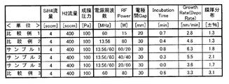
また、微結晶半導体膜の成膜において、成膜条件を多段階に分けて変えることで成膜速度を向上させ、大量生産に向いたプロセスとする。例えば、成膜初期に形成される半導体領域の品質を向上するため、ゲート電極上にゲート絶縁膜を形成した後、成膜速度は低いが品質のよい第1の成膜条件でゲート絶縁膜界面付近の微結晶半導体膜の下部を形成し、その後、高い成膜速度の第2の成膜条件に変えて微結晶半導体膜の上部を堆積する。 Further, in the formation of a microcrystalline semiconductor film, the film formation condition is changed in multiple stages to improve the film formation speed, and the process is suitable for mass production. For example, in order to improve the quality of the semiconductor region formed at the initial stage of film formation, after forming a gate insulating film on the gate electrode, the interface of the gate insulating film is formed under a first film forming condition with low film formation speed but good quality. A lower part of the microcrystalline semiconductor film in the vicinity is formed, and then the upper part of the microcrystalline semiconductor film is deposited under the second film formation condition at a high film formation rate.
成膜速度は低いが品質のよい第1の成膜条件としては、予め成膜前に真空チャンバー(反応容器)内の酸素やH2Oなどのガスの残留を極力低減するため、到達最低圧力を1×10⁻¹⁰〜1×10⁻⁷Torr(約1×10⁻⁸Paを超え1×10⁻⁵Pa以下)の超高真空(UHV)領域に下げ、高い純度の材料ガスを流し、成膜時の基板温度を100℃以上300℃未満の範囲とする。また、表面定在波の影響が出ない高周波電力と、VHF帯に属する高周波電力との両方を印加してプラズマを形成する。異なる周波数の高周波電力を印加する、即ち重畳印加することによりインキュベーション時間を大幅に減少または解消することができ、膜質の均一性を向上させることができる。微結晶半導体膜は成膜開始とともに膜厚が増加するのではなく、成膜を開始してから暫くは膜がほとんど成長せずに、ある程度時間が経ってから膜成長の速度が急に増加するという現象が生じることがある。この成膜開始から有効な膜成長が始まるまでの時間をインキュベーション時間と呼び、このインキュベーション時間はわずかではあるが、存在することで膜質の不均一性を招く恐れがある。また、膜の堆積開始時にこのようなインキュベーション時間が存在するとプロセスのスループットが低下する恐れがある。 As the first film formation condition with a low film formation speed but good quality, it is necessary to reduce the residual pressure of gases such as oxygen and H 2 O in the vacuum chamber (reaction vessel) in advance before film formation. To 1 × 10 −10 to 1 × 10 −7 Torr (over about 1 × 10 −8 Pa to 1 × 10 −5 Pa or less) ultra high vacuum (UHV) region, flowing a high-purity material gas, The substrate temperature during film formation is set to a range of 100 ° C. or higher and lower than 300 ° C. In addition, plasma is formed by applying both high-frequency power that is not affected by surface standing waves and high-frequency power that belongs to the VHF band. By applying high-frequency power of different frequencies, that is, by superimposing, the incubation time can be greatly reduced or eliminated, and the film quality uniformity can be improved. The film thickness of the microcrystalline semiconductor film does not increase with the start of film formation. The film growth rate does not increase for a while after the film formation starts, and the film growth rate suddenly increases after a certain amount of time. May occur. The time from the start of film formation to the start of effective film growth is called the incubation time. Although this incubation time is small, the presence of it may cause non-uniformity in film quality. Also, the presence of such an incubation time at the start of film deposition can reduce process throughput.
本明細書で開示する発明の構成は、絶縁表面を有するガラス基板上にゲート電極を形成し、該ゲート電極上に絶縁膜を成膜し、ガラス基板を真空チャンバー内に導入し、真空チャンバー内に材料ガスを導入し、該真空チャンバー内にグロー放電プラズマを生成する電極に、波長10m以上の周波数を有する第1の高周波電力と、波長10m未満の周波数を有する第2の高周波電力とを重畳印加してグロー放電プラズマを生成する第1の成膜条件により微結晶半導体膜の下部を成膜し、上記第1の成膜条件と、基板温度、電力、周波数、材料ガス流量、または真空度の少なくとも1つの条件が異なる第2の成膜条件で上記真空チャンバーと同一チャンバー内で微結晶半導体膜の上部を堆積し、前記微結晶半導体膜上にバッファ層を成膜する半導体装置の作製方法である。 In the structure of the invention disclosed in this specification, a gate electrode is formed over a glass substrate having an insulating surface, an insulating film is formed over the gate electrode, and the glass substrate is introduced into a vacuum chamber. A material gas is introduced into the electrode, and a first high-frequency power having a frequency of 10 m or more and a second high-frequency power having a frequency of less than 10 m are superimposed on an electrode for generating glow discharge plasma in the vacuum chamber. A lower portion of the microcrystalline semiconductor film is formed under a first film formation condition for generating glow discharge plasma by applying the first film formation condition, the substrate temperature, power, frequency, material gas flow rate, or degree of vacuum. A semiconductor layer in which an upper portion of a microcrystalline semiconductor film is deposited in the same chamber as the vacuum chamber under a second film forming condition in which at least one of the conditions is different, and a buffer layer is formed on the microcrystalline semiconductor film Device, which is a method for manufacturing.
上記第1の成膜条件で得られる微結晶半導体膜の下部は、膜中の酸素濃度が1×10¹⁷/cm以下である。微結晶半導体膜の成膜の際、酸素は結晶化を阻害し、シリコン膜中に取り込まれた場合にはドナーとして作用する恐れがあるため、特に低減すべき不純物である。この第1の成膜条件で得られる微結晶半導体膜の下部の品質が、後に形成されるTFTのオン電流増大および電界効果移動度の向上に寄与する。 The oxygen concentration in the lower part of the microcrystalline semiconductor film obtained under the first deposition condition is 1 × 10 17 / cm or less. When the microcrystalline semiconductor film is formed, oxygen is an impurity to be particularly reduced because it inhibits crystallization and may act as a donor when taken into the silicon film. The quality of the lower portion of the microcrystalline semiconductor film obtained under the first deposition condition contributes to an increase in on-current and field effect mobility of a TFT to be formed later.
また、微結晶半導体膜の成膜前に予め、真空チャンバーをベーキング(200℃以上300℃以下)して真空チャンバー内に存在する水分を主成分とする残留ガスを取り除き、真空チャンバー内を超高真空領域の真空度の圧力環境にすることが好ましい。また、微結晶半導体膜の成膜中も真空チャンバー内壁を加熱(50℃以上300℃以下)して成膜反応を促進させてもよい。 In addition, before the microcrystalline semiconductor film is formed, the vacuum chamber is baked (200 ° C. or higher and 300 ° C. or lower) to remove residual gas containing moisture as a main component in the vacuum chamber. It is preferable to use a pressure environment having a degree of vacuum in the vacuum region. Further, the inner wall of the vacuum chamber may be heated (from 50 ° C. to 300 ° C.) during the formation of the microcrystalline semiconductor film to promote the film formation reaction.
また、第2の成膜条件としては、少なくとも第1の成膜条件の成膜速度よりも速い成膜速度が得られる条件とすればよく、例えば、シランガスと水素ガスの流量比を第1の成膜条件とは変えて微結晶シリコン膜が形成される範囲内で水素濃度を下げればよい。また、第2の成膜条件としては、第1の成膜条件の基板温度よりも高い温度、例えば300℃以上の基板温度として成膜速度を速くしてもよい。また、第2の成膜条件として、第1の成膜条件よりも電力を増大させることにより、成膜速度を速くしてもよい。また、真空チャンバーのコンダクタンスバルブなどの排気バルブを調節して第2の成膜条件を第1の成膜条件と異なる真空度として成膜速度を速くしてもよい。 The second film formation condition may be a condition that at least a film formation speed higher than the film formation speed of the first film formation condition may be obtained. For example, the flow rate ratio of silane gas and hydrogen gas is set to the first film formation speed. The hydrogen concentration may be lowered within the range in which the microcrystalline silicon film is formed, instead of the film formation conditions. Further, as the second film formation condition, the film formation rate may be increased by setting the temperature higher than the substrate temperature of the first film formation condition, for example, a substrate temperature of 300 ° C. or higher. Further, as the second film formation condition, the film formation rate may be increased by increasing the electric power as compared with the first film formation condition. Further, the film formation speed may be increased by adjusting the exhaust valve such as the conductance valve of the vacuum chamber so that the second film formation condition is different from the first film formation condition.
また、第1の成膜条件よりも成膜速度を速くする第2の成膜条件として、VHF帯の高周波電力をパルスで供給することで、成膜時において気相中で粉体が異常成長することを防ぐことができる。粉体の成長を抑えるためには、気体分子の平均滞留時間を考慮する必要があるが、パルスの発振周波数を概略1〜100kHzとすれば良い。 In addition, as a second film forming condition in which the film forming speed is made faster than the first film forming condition, the high-frequency power in the VHF band is supplied in pulses, whereby the powder grows abnormally in the gas phase at the time of film forming. Can be prevented. In order to suppress the growth of the powder, it is necessary to consider the average residence time of the gas molecules, but the pulse oscillation frequency may be approximately 1 to 100 kHz.
また、第1の成膜条件よりも成膜速度を速くする第2の成膜条件として、微結晶半導体膜を成膜する真空チャンバーの内壁を基板温度よりも高い温度で加熱し、微結晶半導体膜を成膜してもよい。第1の成膜条件における基板温度が100℃であれば、真空チャンバーの内壁を150℃とすることで、チャンバー内壁よりも低温の基板表面に微結晶半導体膜を効率よく形成する。 In addition, as a second film formation condition for increasing the film formation rate than the first film formation condition, the inner wall of the vacuum chamber for forming the microcrystalline semiconductor film is heated at a temperature higher than the substrate temperature, and the microcrystalline semiconductor is formed. A film may be formed. If the substrate temperature in the first film formation condition is 100 ° C., the inner wall of the vacuum chamber is set to 150 ° C., whereby the microcrystalline semiconductor film is efficiently formed on the substrate surface at a temperature lower than that of the chamber inner wall.
また、真空チャンバー内の雰囲気中を1×10⁻⁸Paを超え1×10⁻⁵Pa以下の真空度に真空排気した後、基板導入前に予め、真空チャンバー内に水素ガスまたは希ガスを導入してプラズマを発生させ、真空チャンバー内に存在する水分を主成分とする残留ガスを取り除き、真空チャンバー内の残留酸素濃度を低減させた環境にすることが好ましい。 In addition, after evacuating the atmosphere in the vacuum chamber to a degree of vacuum exceeding 1 × 10 −8 Pa to 1 × 10 −5 Pa or less, hydrogen gas or a rare gas is introduced into the vacuum chamber in advance before introducing the substrate. Thus, it is preferable to create an environment in which plasma is generated and residual gas mainly containing moisture present in the vacuum chamber is removed to reduce the residual oxygen concentration in the vacuum chamber.
また、真空チャンバー内の雰囲気中を1×10⁻⁸Paを超え1×10⁻⁵Pa以下の真空度に真空排気した後、基板導入前に予め、シランガスを真空チャンバー内に流し、真空チャンバー内の残留酸素と反応させ酸化珪素に変えることで、さらに真空チャンバー内の酸素を低減してもよい。また、微結晶半導体膜の成膜中に混入するアルミニウムなどの金属元素の混入を防止するため、基板導入前に予め、シランガスを真空チャンバー内に流し、プラズマを発生させて内壁に成膜する処理(プレコート処理とも呼ぶ)を行ってもよい。 Further, after evacuating the atmosphere in the vacuum chamber to a degree of vacuum of more than 1 × 10 −8 Pa and not more than 1 × 10 −5 Pa, silane gas is allowed to flow in the vacuum chamber in advance before introducing the substrate. The oxygen in the vacuum chamber may be further reduced by reacting with the remaining oxygen and changing to silicon oxide. In addition, in order to prevent the mixing of metal elements such as aluminum mixed during the formation of the microcrystalline semiconductor film, a process of forming a film on the inner wall by flowing a silane gas into the vacuum chamber in advance before introducing the substrate and generating plasma. (Also referred to as pre-coating treatment) may be performed.
第1の成膜条件は、成膜速度が遅いため、特に膜厚を厚くすると成膜時間が長くなり、その結果、膜中に酸素などの不純物が混入しやすい。従って、このように、基板導入前に真空チャンバー内の酸素及び水分を十分に低減することによって、成膜時間が長くなっても膜中の酸素などの不純物がほとんど混入されず、後に成膜する微結晶シリコン膜の品質を向上させる上で重要である。 The first film forming condition is that the film forming speed is slow. Therefore, when the film thickness is increased, the film forming time becomes longer. As a result, impurities such as oxygen are likely to be mixed into the film. Therefore, by sufficiently reducing oxygen and moisture in the vacuum chamber before introducing the substrate in this way, impurities such as oxygen in the film are hardly mixed even when the film formation time is long, and the film is formed later. This is important for improving the quality of the microcrystalline silicon film.
さらに、基板導入後、微結晶シリコン膜の成膜前に予め、基板上の吸着水を除去するため、アルゴンプラズマ処理などの希ガスプラズマ処理及び水素プラズマ処理を行って、微結晶シリコン膜中の酸素濃度を1×10¹⁷/cm以下に低減してもよい。 Further, in order to remove adsorbed water on the substrate in advance after the introduction of the substrate and before the formation of the microcrystalline silicon film, a rare gas plasma treatment such as an argon plasma treatment and a hydrogen plasma treatment are performed. The oxygen concentration may be reduced to 1 × 10 17 / cm or less.
このように、基板導入後に基板が有する酸素及び水分を十分に低減することも、後に成膜する微結晶シリコン膜の品質を向上させる上で重要である。 As described above, it is important to sufficiently reduce oxygen and moisture of the substrate after introduction of the substrate in order to improve the quality of the microcrystalline silicon film to be formed later.
また、成膜初期(第1の成膜期間)の第1の成膜条件から成膜後期の高い成膜速度の第2の成膜条件(第2の成膜期間)に変えることによって、成膜初期に微結晶が形成されているため、成膜後期では、成膜初期で得られた微結晶を核として品質の高い微結晶シリコン膜を堆積することができる。また、成膜初期に予め、微結晶を形成しておくことにより成膜後期の成膜速度を速くすることができる。 Further, by changing from the first film formation condition at the initial stage of film formation (first film formation period) to the second film formation condition (second film formation period) at a high film formation speed at the later stage of film formation. Since microcrystals are formed in the initial stage of the film, a high-quality microcrystalline silicon film can be deposited using the microcrystals obtained in the initial stage of film formation as nuclei. In addition, by forming a microcrystal in advance at the initial stage of film formation, the film formation rate at the latter stage of film formation can be increased.
成膜条件を途中で変えずに第1の成膜条件のみで所望の膜厚を得る時間に比べて、第1の成膜条件での成膜の後に引き続き同じチャンバーで第2の成膜条件での成膜を行うことで、所望の膜厚を得る時間を短縮することができる。所望の膜厚を得る時間を短縮することができれば、微結晶シリコン膜中に酸素などの不純物がほとんど混入されずに成膜を行うことができる。また、成膜条件を途中で変えずに第1の成膜条件のみで微結晶シリコン膜の膜厚を薄くすると、後に積層するバッファ層の影響が大きくなり、薄膜トランジスタの電界効果移動度が低下する恐れがある。 Compared to the time for obtaining a desired film thickness only with the first film formation condition without changing the film formation condition in the middle, the second film formation condition continues in the same chamber after the film formation under the first film formation condition. By performing the film formation at, the time for obtaining a desired film thickness can be shortened. If the time for obtaining a desired film thickness can be shortened, the microcrystalline silicon film can be formed with almost no impurities such as oxygen mixed therein. In addition, when the film thickness of the microcrystalline silicon film is reduced only by the first film formation condition without changing the film formation condition in the middle, the influence of a buffer layer to be stacked later is increased, and the field effect mobility of the thin film transistor is decreased. There is a fear.
また、上記第1の成膜条件で得られる微結晶シリコン膜は、酸素に反応しやすいため、高い成膜速度の第2の成膜条件に成膜途中で変えて成膜することによってゲート絶縁膜界面付近の膜を保護することができる。この第2の成膜条件で得られる微結晶シリコン膜の品質が、後に形成されるTFTのオフ電流低減にも寄与する。 In addition, since the microcrystalline silicon film obtained under the first film formation condition is easy to react with oxygen, the film is changed to the second film formation condition at a high film formation speed during the film formation to form a gate insulating film. The film near the film interface can be protected. The quality of the microcrystalline silicon film obtained under the second film formation condition also contributes to reduction of off-current of a TFT to be formed later.
こうして成膜条件を2段階に変化させて得られる微結晶シリコン膜は、少なくとも柱状の結晶を含んでおり、膜中の酸素濃度が1×10¹⁷/cm以下である。また、2段階に変化させて得られる微結晶シリコン膜の合計膜厚は、5nm〜100nm、好ましくは10nm〜30nmの範囲とする。 A microcrystalline silicon film obtained by changing the deposition conditions in two stages in this way includes at least columnar crystals, and the oxygen concentration in the film is 1 × 10 17 / cm or less. The total film thickness of the microcrystalline silicon film obtained by changing in two steps is in the range of 5 nm to 100 nm, preferably 10 nm to 30 nm.
初期の成膜条件が品質の高い微結晶シリコン膜を形成する条件であれば、成膜条件を2段階に変化させて微結晶シリコン膜を形成することに限定されず、3段階以上に変化させて成膜することもできる。さらに成膜条件を連続的に変化させることもできる。成膜条件を連続的に変化させるとは、単位時間あたりのレベル変化を連続的に生じさせることであり、例えば、チャンバー内に導入する材料ガス(シランガス等)の平均流量を時間経過に伴って増加させ、ガス流量と時間との関係をグラフ(縦軸をガス流量、横軸を時間とするグラフ)で示した時に右上がりの直線または右上がりの曲線を描くことを指している。或いはチャンバー内に導入するシランガスなどの流量を一定または増加させ、その他のガス(水素、希ガスなど)の平均流量を時間経過に伴って減少させて、その他のガス流量と時間との関係をグラフで示した時に右下がりの直線または右下がりの曲線を描くことを指している。連続的に変化させることは、少なくとも大気に触れることなく成膜条件を変えて1枚の基板に成膜を行うことを指している。 If the initial film formation conditions are conditions for forming a high-quality microcrystalline silicon film, the film formation conditions are not limited to forming the microcrystalline silicon film in two stages, but are changed in three or more stages. It is also possible to form a film. Furthermore, the film forming conditions can be changed continuously. Continuously changing the film forming conditions is to cause a level change per unit time continuously. For example, the average flow rate of the material gas (such as silane gas) introduced into the chamber is increased with time. When the relationship between the gas flow rate and the time is shown as a graph (a graph in which the vertical axis represents the gas flow rate and the horizontal axis represents time), this indicates that a straight line rising to the right or a curve rising to the right is drawn. Alternatively, the flow rate of silane gas or the like introduced into the chamber is constant or increased, and the average flow rate of other gases (hydrogen, rare gas, etc.) is decreased over time, and the relationship between the flow rate of other gases and time is graphed. This means to draw a straight line or a downward curve. To change continuously refers to performing film formation on a single substrate while changing film formation conditions at least without exposure to the atmosphere.
また、上記微結晶シリコン膜は、非晶質シリコン膜に比べて酸素に反応しやすいため、さらに大気にさらすことなく、結晶粒を含まないバッファ層を積層して保護することが好ましい。バッファ層は、微結晶シリコン膜を成膜する真空チャンバーと異なる真空チャンバーで上記第1の成膜条件及び上記第2の成膜条件よりも高い基板温度、例えば300℃以上400℃未満とする。バッファ層の成膜時の基板温度を上記第1の成膜条件及び上記第2の成膜条件よりも高い基板温度とすることは有用である。なぜなら、工程を増やすことなく、バッファ層の成膜時に微結晶シリコン膜をアニールすることができ、微結晶シリコン膜の膜質を向上させることができるからである。バッファ層の成膜時に微結晶シリコン膜をアニールすることにより、電圧印加を繰り返し行う信頼性試験におけるTFT特性の変動(閾値の変動など)も抑え、TFTの信頼性も向上させることができる。バッファ層は、代表的には、100nm以上400nm以下、好ましくは200nm以上300nm以下の厚さで形成する。また、バッファ層は、上記微結晶シリコン膜よりも欠陥密度の高い非晶質シリコン膜を用いる。バッファ層に欠陥密度の高い非晶質シリコン膜を用いることで、後に形成されるTFTのオフ電流低減に寄与する。 The microcrystalline silicon film is more susceptible to oxygen than an amorphous silicon film, and thus it is preferable to protect the microcrystalline silicon film by stacking a buffer layer that does not contain crystal grains without being exposed to the atmosphere. The buffer layer has a substrate temperature higher than the first film formation condition and the second film formation condition in a vacuum chamber different from the vacuum chamber in which the microcrystalline silicon film is formed, for example, 300 ° C. or higher and lower than 400 ° C. It is useful to set the substrate temperature at the time of forming the buffer layer to a substrate temperature higher than the first film forming condition and the second film forming condition. This is because the microcrystalline silicon film can be annealed when the buffer layer is formed without increasing the number of steps, and the film quality of the microcrystalline silicon film can be improved. By annealing the microcrystalline silicon film during the formation of the buffer layer, fluctuations in TFT characteristics (threshold fluctuations and the like) in a reliability test in which voltage application is repeatedly performed can be suppressed, and the reliability of the TFT can be improved. The buffer layer is typically formed with a thickness of 100 nm to 400 nm, preferably 200 nm to 300 nm. As the buffer layer, an amorphous silicon film having a defect density higher than that of the microcrystalline silicon film is used. By using an amorphous silicon film having a high defect density for the buffer layer, it contributes to a reduction in off-current of a TFT to be formed later.
また、上記微結晶シリコン膜は、不純物が混入してn型の導電性を示しやすいため、材料ガスにトリメチルボロンガスなどを微量に加えて、i型となるように成膜条件を調節することが好ましい。シランガス及び水素ガスが主の材料ガスにトリメチルボロンガスなどを微量に加えることによって、薄膜トランジスタのしきい値制御が可能となる。 In addition, since the microcrystalline silicon film easily exhibits n-type conductivity due to impurities mixed therein, a film formation condition is adjusted to be i-type by adding a small amount of trimethylboron gas or the like to the material gas. Is preferred. By adding a small amount of trimethylboron gas or the like to silane gas and hydrogen gas as the main material gas, the threshold value of the thin film transistor can be controlled.
なお、本明細書において、微結晶半導体膜とは、非晶質と結晶構造(単結晶、多結晶を含む)の中間的な構造の半導体を含む膜である。この半導体は、自由エネルギー的に安定な第3の状態を有する半導体であって、短距離秩序を持ち格子歪みを有する結晶質なものであり、粒径が0.5〜20nmの柱状または針状結晶が基板表面に対して法線方向に成長している。また、微結晶半導体と非単結晶半導体とが混在している。微結晶半導体の代表例である微結晶シリコンは、そのラマンスペクトルが単結晶シリコンを示す520.5cm−1よりも低波数側に、シフトしている。即ち、単結晶シリコンを示す520.5cm−1とアモルファスシリコンを示す480cm−1の間に微結晶シリコンのラマンスペクトルのピークがある。また、未結合手(ダングリングボンド)を終端するため水素またはハロゲンを少なくとも1原子%またはそれ以上含ませている。さらに、ヘリウム、アルゴン、クリプトン、ネオンなどの希ガス元素を含ませて格子歪みをさらに助長させることで、安定性が増し良好な微結晶半導体膜が得られる。このような微結晶半導体膜に関する記述は、例えば、米国特許4,409,134号で開示されている。 Note that in this specification, a microcrystalline semiconductor film is a film including a semiconductor having an intermediate structure between amorphous and crystalline structures (including single crystal and polycrystal). This semiconductor is a semiconductor having a third state which is stable in terms of free energy, and is a crystalline one having a short-range order and having a lattice strain, and has a columnar or needle shape with a particle size of 0.5 to 20 nm. Crystals grow in the normal direction with respect to the substrate surface. In addition, a microcrystalline semiconductor and a non-single-crystal semiconductor are mixed. Microcrystalline silicon which is a typical example of a microcrystalline semiconductor has its Raman spectrum shifted to a lower wave number than 520.5 cm −1 indicating single crystal silicon. That is, the peak of the Raman spectrum of microcrystalline silicon is between 520.5 cm −1 representing single crystal silicon and 480 cm −1 representing amorphous silicon. In addition, at least 1 atomic% or more of hydrogen or halogen is contained to terminate dangling bonds (dangling bonds). Further, by adding a rare gas element such as helium, argon, krypton, or neon to further promote lattice distortion, stability can be improved and a good microcrystalline semiconductor film can be obtained. A description of such a microcrystalline semiconductor film is disclosed in, for example, US Pat. No. 4,409,134.
また、大面積のガラス基板の処理を複数枚行うときスループット上で不利となるが、微結晶シリコン膜を成膜する真空チャンバーと同じ真空チャンバーでバッファ層を形成してもよい。同じ真空チャンバーでバッファ層を形成すれば、基板搬送中、浮遊する汚染不純物に汚染されることなく積層界面を形成することができるので、薄膜トランジスタ特性のばらつきを低減することができる。特に大面積のガラス基板の基板搬送は、小型の基板に比べて長時間要するため、汚染不純物が付着する恐れがあり、同じ真空チャンバーで形成することは、有用である。 Further, when a plurality of large-sized glass substrates are processed, the throughput is disadvantageous. However, the buffer layer may be formed in the same vacuum chamber as the vacuum chamber in which the microcrystalline silicon film is formed. If the buffer layer is formed in the same vacuum chamber, a stacked interface can be formed without being contaminated by floating contaminants during substrate transport, so that variations in thin film transistor characteristics can be reduced. In particular, since a large-area glass substrate needs to be transported for a long time compared to a small-sized substrate, there is a risk of contamination impurities adhering, and it is useful to form the substrate in the same vacuum chamber.
また、バッファ層上にはソース電極またはドレイン電極を形成し、それらソース電極及びドレイン電極の間のリーク電流を下げるために、バッファ層に溝を形成している。 Further, a source electrode or a drain electrode is formed on the buffer layer, and a groove is formed in the buffer layer in order to reduce a leakage current between the source electrode and the drain electrode.
また、バッファ層とソース電極またはドレイン電極の間には、n型不純物元素を含む半導体膜(n+層)を有している。また、バッファ層は、n+層と微結晶シリコン膜とが接しないように、これらの間に設けられている。従って、ソース電極の下方には、n+層、バッファ層、微結晶シリコン膜が重なっている。同様にドレイン電極の下方には、n+層、バッファ層、微結晶シリコン膜が重なっている。このような積層構造とし、バッファ層の膜厚を厚くすることで、耐圧向上を図っている。また、バッファ層の膜厚を厚く成膜しておけば、酸化しやすい微結晶シリコン膜を露出させることなくバッファ層の一部に溝を形成することができる。 In addition, a semiconductor film (n + layer) containing an n-type impurity element is provided between the buffer layer and the source or drain electrode. Further, the buffer layer is provided between the n + layer and the microcrystalline silicon film so as not to contact each other. Therefore, an n + layer, a buffer layer, and a microcrystalline silicon film are overlapped below the source electrode. Similarly, an n + layer, a buffer layer, and a microcrystalline silicon film are overlapped below the drain electrode. With such a laminated structure, the breakdown voltage is improved by increasing the thickness of the buffer layer. In addition, if the buffer layer is formed thick, a groove can be formed in a part of the buffer layer without exposing the microcrystalline silicon film that is easily oxidized.
上記作製工程に引き続き、さらに、バッファ層上にn型不純物元素を含む半導体膜を成膜し、該n型不純物元素を含む半導体膜上にソース電極またはドレイン電極を形成し、n型不純物元素を含む半導体膜をエッチングして、ソース領域及びドレイン領域を形成し、前記ソース領域及び前記ドレイン領域と重なる領域を残存させて前記バッファ層の一部をエッチングして除去して薄膜トランジスタを作製する。 Following the above manufacturing process, a semiconductor film containing an n-type impurity element is further formed over the buffer layer, a source electrode or a drain electrode is formed over the semiconductor film containing the n-type impurity element, and the n-type impurity element is formed. A semiconductor film is etched to form a source region and a drain region, and a region overlapping with the source region and the drain region is left, and a part of the buffer layer is removed by etching to form a thin film transistor.
こうして得られた薄膜トランジスタは、オン動作時に第1の成膜条件で成膜した品質の高い微結晶シリコン膜におけるゲート絶縁膜界面付近の領域がチャネル形成領域として機能し、オフ時には、バッファ層が一部エッチングされた溝の部分がごく微量のリーク電流が流れる経路となる。従って、従来のアモルファスシリコン単層を有する薄膜トランジスタや微結晶シリコン単層を有する薄膜トランジスタに比べて、オフ電流とオン電流の比を大きくすることができ、スイッチング特性に優れていると言え、表示パネルのコントラスト向上につながる。 In the thin film transistor thus obtained, a region in the vicinity of the gate insulating film interface in the high-quality microcrystalline silicon film formed under the first film formation condition during the on-operation functions as a channel formation region, and the buffer layer is integrated in the off state. The part of the groove that has been partially etched becomes a path through which a very small amount of leakage current flows. Therefore, compared with a thin film transistor having a single amorphous silicon layer or a thin film transistor having a microcrystalline silicon single layer, the ratio of off-state current to on-state current can be increased, and the switching characteristics are excellent. This leads to improved contrast.
本発明の作製方法により、表面定在波の影響が出ない高周波電力とVHF帯に属する高周波電力を供給してプラズマを生成することで、長辺が2000mmを超える大面積のガラス基板に均質で品質の良い微結晶半導体膜をチャネル形成領域とする半導体装置を作製することができる。得られる薄膜トランジスタの電界効果移動度を1より大きく50以下とすることができる。このため、本発明の作製方法により得られる微結晶半導体膜を用いた薄膜トランジスタは、電流電圧特性を示す曲線の立ち上がり部分の傾きが急峻となり、スイッチング素子としての応答性が優れ、高速動作が可能となる。 According to the manufacturing method of the present invention, plasma is generated by supplying high-frequency power that does not affect the surface standing wave and high-frequency power that belongs to the VHF band, so that the long side is homogeneous on a large-area glass substrate exceeding 2000 mm. A semiconductor device in which a high-quality microcrystalline semiconductor film is used as a channel formation region can be manufactured. The field effect mobility of the thin film transistor obtained can be greater than 1 and 50 or less. Therefore, a thin film transistor using a microcrystalline semiconductor film obtained by the manufacturing method of the present invention has a steep slope at a rising portion of a curve indicating current-voltage characteristics, has excellent responsiveness as a switching element, and can operate at high speed. Become.
本発明の作製方法により得られる薄膜トランジスタを用いた発光装置は、薄膜トランジスタの閾値の変動を抑制することが可能であり、信頼性の向上に繋がる。 A light-emitting device using a thin film transistor obtained by the manufacturing method of the present invention can suppress a change in threshold value of the thin film transistor, which leads to improvement in reliability.
また、本発明の作製方法により得られる薄膜トランジスタを用いた液晶表示装置は、電界効果移動度を大きくできるため、駆動回路の駆動周波数を高くすることが可能となる。駆動回路を高速に動作させることが出来るため、フレーム周波数を4倍とすること、または、黒画面挿入することなども実現することができる。 In addition, a liquid crystal display device using a thin film transistor obtained by the manufacturing method of the present invention can increase the field-effect mobility; therefore, the driving frequency of the driver circuit can be increased. Since the drive circuit can be operated at high speed, it is possible to realize a quadruple frame frequency or insertion of a black screen.
本発明の実施形態について、以下に説明する。但し、本発明は多くの異なる態様で実施することが可能であり、本発明の趣旨及びその範囲から逸脱することなくその形態及び詳細を様々に変更し得ることは当業者であれば容易に理解される。従って、本実施の形態の記載内容に限定して解釈されるものではない。 Embodiments of the present invention will be described below. However, the present invention can be implemented in many different modes, and those skilled in the art can easily understand that the modes and details can be variously changed without departing from the spirit and scope of the present invention. Is done. Therefore, the present invention is not construed as being limited to the description of this embodiment mode.
(実施の形態1)
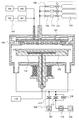
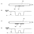
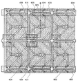
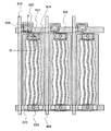
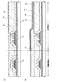
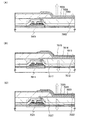
本実施の形態では、液晶表示装置に用いられる薄膜トランジスタの作製工程について、図1乃至図6を用いて説明する。図1乃至図3は、薄膜トランジスタの作製工程を示す断面図であり、図4は、一画素における薄膜トランジスタ及び画素電極の接続領域の上面図である。また、図5は、微結晶シリコン膜の成膜方法を示すタイミングチャートである。また、図6は、周波数の異なる二以上の高周波電力を供給してグロー放電プラズマを生成できるプラズマCVD装置の一構成例を示す断面図である。
(Embodiment 1)
In this embodiment, a manufacturing process of a thin film transistor used for a liquid crystal display device will be described with reference to FIGS. 1 to 3 are cross-sectional views illustrating a manufacturing process of a thin film transistor, and FIG. 4 is a top view of a connection region between a thin film transistor and a pixel electrode in one pixel. FIG. 5 is a timing chart showing a method for forming a microcrystalline silicon film. FIG. 6 is a cross-sectional view showing a configuration example of a plasma CVD apparatus capable of generating glow discharge plasma by supplying two or more high-frequency powers having different frequencies.
微結晶半導体膜を有する薄膜トランジスタはp型よりもn型の方が、電界効果移動度が高いので駆動回路に用いるのにより適している。同一の基板上に形成する薄膜トランジスタを全て同じ極性にそろえておくことが、工程数を抑えるためにも望ましい。ここでは、nチャネル型の薄膜トランジスタを用いて説明する。 A thin film transistor including a microcrystalline semiconductor film is more suitable for use in a driver circuit because an n-type thin film transistor has higher field-effect mobility than a p-type. In order to reduce the number of steps, it is desirable that all thin film transistors formed over the same substrate have the same polarity. Here, description is made using an n-channel thin film transistor.
図1(A)に示すように、基板50上にゲート電極を形成する。基板50は、バリウムホウケイ酸ガラス、アルミノホウケイ酸ガラス、若しくはアルミノシリケートガラスなど、フュージョン法やフロート法で作製される無アルカリガラス基板を用いることができる。基板50がマザーガラスの場合、基板の大きさは、第1世代(300mm×400mm)、第2世代(400mm×500mm)、第3世代(550mm×650mm)、第4世代(730mm×920mm)、第5世代(1000mm×1200mm)、第6世代(2450mm×1850mm)、第7世代(1870mm×2200mm)、第8世代(2000mm×2400mm)、第9世代(2450mm×3050mm)、第10世代(2850mm×3050mm)等を用いることができる。
As shown in FIG. 1A, a gate electrode is formed over the
ゲート電極は、チタン、モリブデン、クロム、タンタル、タングステン、アルミニウムなどの金属材料またはその合金材料を用いて形成する。ゲート電極は、スパッタリング法や真空蒸着法やCVD法で基板50上に導電膜を形成し、当該導電膜上にフォトリソグラフィ技術またはインクジェット法によりマスクを形成し、当該マスクを用いて導電膜をエッチングすることで、形成することができる。また、銀、金、銅などの導電性ナノペーストを用いてインクジェット法により吐出し焼成して、ゲート電極を形成することもできる。なお、ゲート電極の密着性向上と下地への拡散を防ぐバリアメタルとして、上記金属材料の窒化物膜を、基板50とゲート電極の間に設けてもよい。ここでは、第1のフォトマスクを用いて形成したレジストマスクを用いて基板50上に形成された導電膜の積層をエッチングしてゲート電極を形成する。
The gate electrode is formed using a metal material such as titanium, molybdenum, chromium, tantalum, tungsten, or aluminum, or an alloy material thereof. For the gate electrode, a conductive film is formed over the
具体的なゲート電極構造の例としては、第1の導電層51aとなるアルミニウム膜上に第2の導電層51bとなるモリブデン膜を積層させ、アルミニウム特有のヒロックやエレクトロマイグレーションを防ぐ構造にしてもよい。本実施の形態では、大面積の基板を用いて表示画面が大きい表示装置を作製する例であるので、電気抵抗の低いアルミニウムからなる第1の導電層51aと、第1の導電層51aよりも耐熱性の高い第2の導電層51bとを積層させたゲート電極とする。また、アルミニウム膜をモリブデン膜で挟んだ3層構造としてもよい。また、他のゲート電極構造の例として、銅膜上にモリブデン膜の積層、銅膜上に窒化チタン膜の積層、銅膜上に窒化タンタル膜の積層が挙げられる。
As a specific example of the gate electrode structure, a molybdenum film serving as the second
なお、ゲート電極上には半導体膜や配線を形成するので、段切れ防止のため端部がテーパー状になるように加工することが望ましい。また、図示しないがこの工程でゲート電極に接続する配線も同時に形成することができる。 Note that since a semiconductor film or a wiring is formed over the gate electrode, it is preferable to process the end portion to be tapered in order to prevent disconnection. Although not shown, a wiring connected to the gate electrode can be formed at the same time in this step.
次に、ゲート電極の上層である第2の導電層51b上に、ゲート絶縁膜52a、52b、52cを順に形成する。
Next,
ゲート絶縁膜52a、52b、52cはそれぞれ、CVD法やスパッタリング法等を用いて、酸化珪素膜、窒化珪素膜、酸化窒化珪素膜、または窒化酸化珪素膜で形成することができる。ゲート絶縁膜に形成されるピンホール等による層間ショートを防ぐため、異なる絶縁層を用いて多層とすることが好ましい。ここでは、ゲート絶縁膜52a、52b、52cとして、窒化珪素膜、酸化窒化珪素膜、窒化珪素膜の順に積層して形成する形態を示す。
Each of the
ここでは、酸化窒化珪素膜とは、その組成として、窒素よりも酸素の含有量が多いものであって、濃度範囲として酸素が55〜65原子%、窒素が1〜20原子%、Siが25〜35原子%、水素が0.1〜10原子%の範囲で含まれるものをいう。また、窒化酸化珪素膜とは、その組成として、酸素よりも窒素の含有量が多いものであって、濃度範囲として酸素が15〜30原子%、窒素が20〜35原子%、Siが25〜35原子%、水素が15〜25原子%の範囲で含まれるものをいう。 Here, the silicon oxynitride film has a composition that contains more oxygen than nitrogen and has a concentration range of 55 to 65 atomic%, 1 to 20 atomic%, and 25 Si. -35 atomic%, and hydrogen is contained in the range of 0.1-10 atomic%. The silicon nitride oxide film has a composition containing more nitrogen than oxygen, and the concentration ranges of oxygen are 15 to 30 atomic%, nitrogen is 20 to 35 atomic%, and Si is 25 to 25%. 35 atomic% and hydrogen are included in the range of 15 to 25 atomic%.
ゲート絶縁膜の1層目及び2層目の膜厚はともに50nmよりも厚くする。ゲート絶縁膜の1層目は、基板からの不純物(例えばアルカリ金属など)の拡散を防ぐために、窒化珪素膜または窒化酸化珪素膜が好ましい。また、ゲート絶縁膜の1層目は、ゲート電極の酸化防止の他、ゲート電極にアルミニウムを用いる場合にヒロック防止ができる。また、微結晶半導体膜と接するゲート絶縁膜の3層目は、0nmより厚く5nm以下、望ましくは約1nmとする。ゲート絶縁膜の3層目は、微結晶半導体膜との密着性を向上させるために設けるものである。また、ゲート絶縁膜の3層目を窒化珪素膜とすることで後に行われる熱処理やレーザ照射によって、微結晶半導体膜の酸化防止を図ることができる。例えば、酸素の含有量が多い絶縁膜と微結晶半導体膜とを接した状態で熱処理を行うと、微結晶半導体膜が酸化する恐れがある。 The film thicknesses of the first and second layers of the gate insulating film are both greater than 50 nm. The first layer of the gate insulating film is preferably a silicon nitride film or a silicon nitride oxide film in order to prevent diffusion of impurities (for example, alkali metal) from the substrate. The first layer of the gate insulating film can prevent hillocks when aluminum is used for the gate electrode, in addition to preventing oxidation of the gate electrode. The third layer of the gate insulating film in contact with the microcrystalline semiconductor film is thicker than 0 nm and 5 nm or less, preferably about 1 nm. The third layer of the gate insulating film is provided to improve adhesion with the microcrystalline semiconductor film. Further, when the third layer of the gate insulating film is a silicon nitride film, oxidation of the microcrystalline semiconductor film can be prevented by heat treatment or laser irradiation performed later. For example, when heat treatment is performed in a state where an insulating film containing a large amount of oxygen is in contact with a microcrystalline semiconductor film, the microcrystalline semiconductor film may be oxidized.
更には、周波数が1GHzのマイクロ波プラズマCVD装置を用いてゲート絶縁膜を形成することが好ましい。マイクロ波プラズマCVD装置で形成した酸化窒化珪素膜、窒化酸化珪素膜は、耐圧が高く、薄膜トランジスタの信頼性を高めることができる。 Furthermore, it is preferable to form the gate insulating film using a microwave plasma CVD apparatus having a frequency of 1 GHz. A silicon oxynitride film and a silicon nitride oxide film formed with a microwave plasma CVD apparatus have high withstand voltage and can improve the reliability of the thin film transistor.
本実施の形態では、希ガスプラズマ処理、水素プラズマ処理若しくはこの両者の併用により行う下地前処理を行い、続いて成膜処理を行うことが好ましい。また、反応室内は予めゲート絶縁膜と同種の皮膜でコーティングされていることが好ましい。反応室内壁の金属不純物等がゲート絶縁膜中に混入しないようにするためである。 In this embodiment mode, it is preferable to perform base pretreatment performed by rare gas plasma treatment, hydrogen plasma treatment, or a combination of both, followed by film formation. The reaction chamber is preferably coated with the same kind of film as the gate insulating film in advance. This is to prevent metal impurities or the like on the reaction chamber wall from entering the gate insulating film.
反応ガスはシランなどの水素化珪素気体と、酸素若しくは窒素含有気体を反応ガスとして用いる。そして、HF帯(3MHz〜30MHz、代表的には13.56MHz)とVHF帯(30MHz〜300MHz)の高周波電力を重畳印加してグロー放電プラズマを生成する。周波数帯の異なる高周波電力を印加することで、プラズマ密度を高めると共にプラズマ密度の基板面内均一性を高めることができる。ゲート絶縁膜の成膜温度は200℃〜400℃で行うことが好ましく、プラズマ密度が高められることにより緻密で耐圧の高い絶縁膜を形成することができる。ここまでの工程を終えた断面図が図1(A)に相当する。 As the reaction gas, a silicon hydride gas such as silane and an oxygen- or nitrogen-containing gas are used as the reaction gas. Then, high frequency power in the HF band (3 to 30 MHz, typically 13.56 MHz) and the VHF band (30 to 300 MHz) is superimposed and generated to generate glow discharge plasma. By applying high-frequency power in different frequency bands, the plasma density can be increased and the uniformity of the plasma density in the substrate surface can be increased. The gate insulating film is preferably formed at a temperature of 200 ° C. to 400 ° C. When the plasma density is increased, a dense and high withstand voltage insulating film can be formed. A cross-sectional view after the steps up to here corresponds to FIG.
ここでは、ゲート絶縁膜を3層構造としたが、液晶表示装置のスイッチング素子に用いる場合、交流駆動させるため、窒化珪素膜の単層のみでもよい。 Here, the gate insulating film has a three-layer structure, but when used as a switching element of a liquid crystal display device, only a single layer of a silicon nitride film may be used for AC driving.
次いで、ゲート絶縁膜の成膜後、大気に触れさせることなく基板を搬送し、ゲート絶縁膜を成膜する真空チャンバーとは異なる真空チャンバーで微結晶半導体膜53を成膜することが好ましい。
Next, after the gate insulating film is formed, the substrate is transported without exposure to the air, and the
以下に、図5も参照しながら微結晶半導体膜53を形成する手順について説明する。図5の説明は反応室を大気圧から真空排気200する段階から示されており、その後に行われるプレコート201、基板搬入202、下地前処理203、成膜処理204、基板搬出205、クリーニング206の各処理が時系列的に示されている。ただし、大気圧から真空排気することに限定されず、常時ある程度の真空度に反応室を保っておくことが、量産を行う上好ましい、または短時間で到達真空度を下げる上で好ましい。
Hereinafter, a procedure for forming the
本実施の形態では、基板搬入前の真空チャンバー内の真空度を10−5Paよりもさらに高い真空度を確保するために超高真空排気を行う。この段階が図5の真空排気200に対応する。このような超高真空排気を行う場合、ターボ分子ポンプとクライオポンプを併用し、ターボ分子ポンプによる排気を行い、さらにクライオポンプを使って真空排気することが好ましい。また、反応室を加熱処理して内壁からの脱ガス処理を行うことが好ましい。また、基板を加熱するヒータも動作させて温度を安定化させる。基板の加熱温度は100℃以上300℃以下、好ましくは120℃以上220℃以下で行う。
In this embodiment, ultra-high vacuum evacuation is performed in order to secure a degree of vacuum higher than 10 −5 Pa in the vacuum chamber before the substrate is carried. This stage corresponds to the
次いで、基板搬入前にプレコート201を行い、内壁被覆膜としてシリコン膜を形成する。プレコート201として、水素または希ガスを導入してプラズマを発生させて反応室の内壁に付着した気体(酸素及び窒素などの大気成分、若しくは反応室のクリーニングに使用したエッチングガス)を除去した後、シランガスを導入して、プラズマを生成する。シランガスは酸素、水分等と反応するので、シランガスを流し、さらにシランプラズマを生成することで反応室内の酸素、水分を除去することができる。また、プレコート201の処理をしておくことで、微結晶シリコン膜中に反応室を構成する部材の金属元素を不純物として取り込んでしまうのを防ぐことができる。すなわち、反応室内をシリコンで被覆しておくことで、反応室内がプラズマにより食刻されるのを防ぐことができ、後に成膜する微結晶シリコン膜中に含まれる不純物濃度を低減することができる。プレコート201は、反応室の内壁を基板上に堆積されるべき膜と同種の膜で被覆する処理が含まれている。
Next, pre-coating 201 is performed before the substrate is carried in, and a silicon film is formed as an inner wall coating film. As
プレコート201の後、基板搬入202が行われる。微結晶シリコン膜が堆積されるべき基板は、真空排気されたロード室に保管されているので、基板を搬入したとしても反応室内の真空度が著しく悪化することはない。
次いで、下地前処理203を行う。下地前処理203は、微結晶シリコン膜を形成する場合において、特に有効な処理であり行うことが好ましい。すなわち、ガラス基板表面、絶縁膜の表面若しくは非晶質シリコンの表面上に微結晶シリコン膜をプラズマCVD法で成膜する場合には、不純物や格子不整合などの要因により堆積初期段階において非晶質層が形成されてしまう恐れがある。この非晶質層の厚さを極力低減し、可能であれば無くすために下地前処理203を行うことが好ましい。下地前処理としては希ガスプラズマ処理、水素プラズマ処理若しくはこの両者の併用により行うことが好ましい。希ガスプラズマ処理としては、アルゴン、クリプトン、キセノンなど質量数の大きい希ガス元素を用いることが好ましい。表面に付着した酸素、水分、有機物、金属元素などの不純物をスパッタリングの効果で除去するためである。水素プラズマ処理は、水素ラジカルにより、表面に吸着した上記不純物の除去と、絶縁膜若しくは非晶質シリコン膜に対するエッチング作用により清浄な被成膜表面を形成するのに有効である。また、希ガスプラズマ処理と水素プラズマ処理を併用することにより微結晶核生成を促進する作用も期待される。
Next, the
微結晶核の生成を促進させるという意味においては、図5中の破線207で示すように、微結晶シリコン膜の成膜初期においてアルゴンなどの希ガスを供給し続けることは有効である。
In terms of promoting the generation of microcrystalline nuclei, it is effective to continue supplying a rare gas such as argon at the initial stage of the formation of the microcrystalline silicon film, as indicated by a
次いで、下地前処理203に続いて微結晶シリコン膜を形成する成膜処理204を行う。本実施の形態では、成膜速度は低いが品質のよい第1の成膜条件でゲート絶縁膜界面付近の微結晶シリコン膜の下部を形成し、その後、高い成膜速度の第2の成膜条件に変えて微結晶シリコン膜の上部を堆積する。例えば、第1の成膜条件として周波数の異なる2つの高周波電力を重畳印加することにより成膜を行い、第2の成膜条件として重畳印加することなく、3MHz〜30MHzの第3の高周波電力を印加する成膜条件に切り替えて引き続き微結晶半導体膜の成膜を行う。また、第1の成膜条件としては、第1の高周波電力と、前記第1の高周波電力よりも電力の大きい第2の高周波電力とを重畳印加し、第2の成膜条件としては、前記第1の成膜条件よりも電力の大きい第3の高周波電力と、第3の高周波電力よりも電力の小さい第4の高周波電力を印加する成膜条件に切り替えて引き続き微結晶半導体膜の成膜を行う。なお、第3の高周波電力の周波数は、第1の高周波電力と同じであり、第4の高周波電力の周波数は、第2の高周波電力と同じである。
Next, a
第1の成膜条件での成膜速度よりも第2の成膜条件の成膜速度が速ければ特に限定されない。本実施の形態では、HF帯(3MHz〜30MHz、代表的には13.56MHz)の高周波電力とVHF帯(30MHz〜300MHz程度まで)の高周波電力を重畳印加して生成されるグロー放電プラズマを利用するプラズマCVD装置を用いる。図7にHF帯の高周波電力と、VHF帯の高周波電力を重畳させた場合の波形の一例を示す。 There is no particular limitation as long as the deposition rate under the second deposition condition is higher than the deposition rate under the first deposition condition. In this embodiment, glow discharge plasma generated by superimposing high frequency power in the HF band (3 MHz to 30 MHz, typically 13.56 MHz) and high frequency power in the VHF band (up to about 30 MHz to 300 MHz) is used. A plasma CVD apparatus is used. FIG. 7 shows an example of a waveform in a case where high frequency power in the HF band and high frequency power in the VHF band are superimposed.
微結晶シリコン膜は、代表的には、SiH4、Si2H6などの水素化珪素を水素で希釈してプラズマ生成することで成膜することができる。また、水素化珪素及び水素に加え、ヘリウム、アルゴン、クリプトン、ネオンから選ばれた一種または複数種の希ガス元素で希釈して微結晶半導体膜を形成することができる。これらのときの水素化珪素に対して水素の流量比を12倍以上1000倍以下、好ましくは50倍以上200倍以下、更に好ましくは100倍とする。なお、水素化珪素の代わりに、SiH2Cl2、SiHCl3、SiCl4、SiF4等を用いることができる。 A microcrystalline silicon film can be typically formed by diluting silicon hydride such as SiH 4 or Si 2 H 6 with hydrogen to generate plasma. In addition to silicon hydride and hydrogen, the microcrystalline semiconductor film can be formed by dilution with one or more kinds of rare gas elements selected from helium, argon, krypton, and neon. The flow rate ratio of hydrogen to silicon hydride at these times is 12 to 1000 times, preferably 50 to 200 times, and more preferably 100 times. Note that SiH 2 Cl 2 , SiHCl 3 , SiCl 4 , SiF 4, or the like can be used instead of silicon hydride.
また、材料ガスにヘリウムを加えた場合、ヘリウムは24.5eVとすべての気体中で最も高いイオン化エネルギーを持ち、そのイオン化エネルギーよりも少し低い、約20eVの準位に準安定状態があるので、放電持続中においては、イオン化にはその差約4eVしか必要としない。そのため放電開始電圧も全ての気体中最も低い値を示す。このような特性から、ヘリウムはプラズマを安定的に維持することができる。また、均一なプラズマを形成することができるので、微結晶シリコン膜を堆積する基板の面積が大きくなってもプラズマ密度の均一化を図る効果を奏する。 In addition, when helium is added to the material gas, helium has the highest ionization energy of all gases at 24.5 eV, and has a metastable state at a level of about 20 eV, which is slightly lower than the ionization energy. During the discharge duration, the difference requires only about 4 eV for ionization. Therefore, the discharge start voltage also shows the lowest value among all gases. From such characteristics, helium can maintain the plasma stably. In addition, since uniform plasma can be formed, the plasma density can be made uniform even when the area of the substrate on which the microcrystalline silicon film is deposited is increased.
また、シラン等のガス中にCH4、C2H6などの炭素の水素化物、GeH4、GeF4などの水素化ゲルマニウム、フッ化ゲルマニウムを混合して、エネルギーバンド幅を1.5〜2.4eV、若しくは0.9〜1.1eVに調節しても良い。シリコンに炭素又はゲルマニウムを加えるとTFTの温度特性を変えることができる。 In addition, carbon hydride such as CH 4 and C 2 H 6 , germanium hydride such as GeH 4 and GeF 4 , and germanium fluoride are mixed in a gas such as silane so that the energy bandwidth is 1.5-2. It may be adjusted to .4 eV, or 0.9 to 1.1 eV. When carbon or germanium is added to silicon, the temperature characteristics of the TFT can be changed.
ここでは、第1の成膜条件は、シランは水素及び/又は希ガスで100倍を超え2000倍以下に希釈し、基板の加熱温度は100℃以上300℃未満、好ましくは120℃以上220℃以下とする。微結晶シリコンの成長を促進するためには120℃以上220℃以下で成膜を行うことが好ましい。 Here, the first film formation condition is that silane is diluted with hydrogen and / or rare gas to more than 100 times and less than 2000 times, and the heating temperature of the substrate is 100 ° C. or higher and lower than 300 ° C., preferably 120 ° C. or higher and 220 ° C. The following. In order to promote the growth of microcrystalline silicon, the film formation is preferably performed at 120 ° C. or higher and 220 ° C. or lower.
第1の成膜条件を終えた段階での断面図を図1(B)に示す。ゲート絶縁膜52c上には、成膜速度は低いが品質のよい微結晶半導体膜23が成膜されている。この第1の成膜条件で得られる微結晶半導体膜23の品質が、後に形成されるTFTのオン電流増大および電界効果移動度の向上に寄与するため、膜中の酸素濃度が1×10¹⁷/cm以下となるように十分酸素濃度を低減させることが重要である。また、上記手順により、酸素だけでなく、窒素、及び炭素が微結晶半導体膜の膜中に混入する濃度を低減することができるため、微結晶半導体膜がn型化になることを防止することができる。
A cross-sectional view after the first film formation condition is illustrated in FIG. On the
次いで、上記第1の成膜条件から第2の成膜条件に変えて成膜速度を上げて微結晶半導体膜53を成膜する。この段階での断面図が図1(C)に相当する。微結晶半導体膜53の膜厚は、50nm〜500nm(好ましくは100nm〜250nm)の厚さとすれば良い。なお、本実施の形態では、微結晶半導体膜53の成膜時間は、第1の成膜条件で成膜が行われる第1の成膜期間と第2の成膜条件で成膜が行われる第2の成膜期間とを有する。なお、第1の成膜条件で得られる膜を第1の微結晶半導体膜と呼び、第2の成膜条件で得られる膜を第2の微結晶半導体膜と呼ぶこともできるが、成膜後に第1の微結晶半導体膜と第2の微結晶半導体膜の明確な界面を確認することは困難であるため、ここでは成膜途中で条件を変えて得られた積層膜を微結晶半導体膜として表記している。
Next, the
本実施の形態において、第2の成膜条件は、シランは水素及び/又は希ガスで12倍以上100倍以下に希釈し、基板の加熱温度は100℃以上400℃未満、好ましくは220℃以下とする。本実施の形態においてはシランガスの流量を増やすことで、第2の成膜条件の成膜速度を第1の成膜条件よりも速くしたが特に限定されず、HF帯の高周波電力とVHF帯の高周波電力とを印加する条件を変更して第2の成膜条件の成膜速度を第1の成膜条件よりも速くしてもよい。例えば、第1の成膜条件では、図7に示すようにHF帯の高周波電源の出力波形に、VHF帯の高周波電源の出力波形が重畳する電力印加を行い、第2の成膜条件では、図8に示すようにVHF帯の高周波電力のオンオフを繰り返してパルス発振させて一部が重畳する波形として成膜を行ってもよい。 In this embodiment mode, the second film formation condition is that silane is diluted 12 to 100 times with hydrogen and / or a rare gas, and the heating temperature of the substrate is 100 ° C. or higher and lower than 400 ° C., preferably 220 ° C. or lower. And In this embodiment, by increasing the flow rate of the silane gas, the film formation speed of the second film formation condition is made faster than that of the first film formation condition. However, there is no particular limitation, and the high frequency power in the HF band and the VHF band The conditions for applying the high-frequency power may be changed so that the film forming speed of the second film forming condition is faster than that of the first film forming condition. For example, in the first film formation condition, as shown in FIG. 7, power is applied such that the output waveform of the VHF band high frequency power supply is superimposed on the output waveform of the HF band high frequency power supply, and in the second film formation condition, As shown in FIG. 8, film formation may be performed as a waveform in which part of the VHF band high-frequency power is repeatedly turned on and off to cause pulse oscillation.
次いで、第2の成膜条件での微結晶シリコンの成膜が終了した後、次いで、シラン、水素などの材料ガス及び高周波電力の供給を止めて基板搬出205を行う。引き続き次の基板に対して成膜処理を行う場合には、基板搬入202の段階に戻り同じ処理が行われる。反応室内に付着した被膜や粉末を除去するには、クリーニング206を行う。
Next, after film formation of microcrystalline silicon under the second film formation condition is completed, supply of a material gas such as silane and hydrogen and high-frequency power is stopped, and substrate unloading 205 is performed. When the film forming process is subsequently performed on the next substrate, the same process is performed by returning to the substrate carry-in 202 stage.
クリーニング206はNF3、SF6に代表されるエッチングガスを導入してプラズマエッチングを行う。また、ClF3のようにプラズマを利用しなくてもエッチングが可能なガスを導入して行う。クリーニング206においては基板加熱用のヒータを切って、チャンバー内壁温度を下げて行うことが好ましい。エッチングによる反応副生成物の生成を抑えるためである。クリーニング206の終了後はプレコート201に戻り、次の基板に対して上述した同様の処理を行えば良い。
The cleaning 206 performs plasma etching by introducing an etching gas typified by NF 3 and SF 6 . Further, the etching is performed by introducing a gas such as ClF 3 that can be etched without using plasma.
ここで、ゲート絶縁膜や微結晶シリコンの成膜に用いる複数の高周波電力が印加されるプラズマCVD装置の一構成例を図6に示す。 Here, FIG. 6 illustrates a configuration example of a plasma CVD apparatus to which a plurality of high-frequency powers used for forming a gate insulating film or microcrystalline silicon are applied.
反応室100はアルミニウム又はステンレスなど剛性のある素材で形成され、内部を真空排気できるように構成されている。反応室100には第1の電極101と第2の電極102が備えられている。
The
第1の電極101には高周波電力供給手段103が連結され、第2の電極102は接地電位が与えられ、基板を載置できるように構成されている。第1の電極101は絶縁材116により反応室100と絶縁分離され、高周波電力が漏洩しないように構成されている。なお、図6では、第1の電極101と第2の電極102について容量結合型(平行平板型)の構成を示しているが、異なる二以上の高周波電力を印加して反応室100の内部にグロー放電プラズマを生成できるものであれば、誘導結合型など他の構成を適用することもできる。
The
高周波電力供給手段103は、第1の高周波電源104と第2の高周波電源105、及びそれらに対応して第1の整合器106と第2の整合器107が含まれている。第1の高周波電源104と第2の高周波電源105から出力される高周波電力は、共に第1の電極101に供給される。第1の整合器106又は第2の整合器107の出力側には、他方の高周波電力が流入しないように帯域通過フィルタを設けても良い。
The high-frequency power supply means 103 includes a first high-
第1の高周波電源104が供給する高周波電力は、概ね波長として10m以上の高周波が適用され、HF帯である3MHzから30MHz、代表的には13.56MHzの周波数が適用される。第2の高周波電源105が供給する高周波電力は、VHF帯の周波数であり概ね波長が10m未満、すなわち30MHz〜300MHzの高周波電力が適用される。
The high frequency power supplied from the first high
第1の高周波電源104が供給する高周波電力の波長は、第1の電極101の1辺の長さの3倍以上を有し、第2の高周波電源105が供給する高周波の波長は、それよりも短い波長を適用する。表面定在波の影響が出ない高周波電力を第1の電極101に供給してグロー放電プラズマを生成し、VHF帯に属する高周波電力を供給してグロー放電プラズマの高密度化を図ることで、長辺が2000mmを超える大面積基板に均質で膜質の良い薄膜を形成することが可能となる。
The wavelength of the high-frequency power supplied from the first high-
図7は第1の高周波電源104の高周波電力と、第2の高周波電源105の高周波電力を重畳させた場合の波形の一例を示す。HF帯(代表的には13.56MHz)の周波数が適用される第1の高周波電源104の出力波形に、VHF帯の周波数が適用される第2の高周波電源105の出力波形が重畳されることで、プラズマの高密度化を図り、表面定在波の影響を無くしてプラズマ密度の面内均一性を高めることができる。図8は第2の高周波電源105としてパルス発振する電源を用いる場合の一例を概念図として示している。VHF帯の高周波電力をパルスで供給することで、成膜時において気相中で粉体が異常成長することを防ぐことができる。粉体の成長を抑えるためには、気体分子の平均滞留時間を考慮する必要があるが、パルスの発振周波数を概略1〜100kHzとすれば良い。
FIG. 7 shows an example of a waveform when the high-frequency power of the first high-
第1の電極101はガス供給手段108にも連結されている。ガス供給手段108は、反応ガスが充填されるシリンダ110、圧力調整弁111、ストップバルブ112、マスフローコントローラ113などで構成されている。反応室100内において、第1の電極101は基板と対向する面がシャワー板状に加工され、多数の細孔が設けられている。第1の電極101に供給される反応ガスは、この細孔から反応室100内に供給される。
The
図9は第1の電極101の他の構成を示す。第1の電極101は、第1の高周波電源104から高周波電力が供給される第1の電極101aと、第2の高周波電源105から高周波電力が供給される第1の電極101bに分離されている。第1の電極101aと第1の電極101bは基板と対向する面は細孔が設けられると共に、櫛歯状にかみ合うように構成され、隣接するもの同士は接触しないように絶縁材116で分離されている。図9に示す構成は、図6で示す第1の電極101と置き換えることが可能であり、同様な効果を得ることができる。
FIG. 9 shows another configuration of the
反応室100に接続される排気手段109は真空排気と、反応ガスを流す場合において反応室100内を所定の圧力に保持するように制御する機能が含まれている。排気手段109の構成としては、バタフライバルブ117、コンダクタンスバルブ118、ターボ分子ポンプ119、ドライポンプ120などが含まれる。バタフライバルブ117とコンダクタンスバルブ118を並列に配置する場合には、バタフライバルブ117を閉じてコンダクタンスバルブ118を動作させることで、反応ガスの排気速度を制御して反応室100の圧力を所定の範囲に保つことができる。また、コンダクタンスの大きいバタフライバルブ117を開くことで高真空排気が可能となる。
The exhaust means 109 connected to the
真空度として10−5Paよりもさらに高真空にするために超高真空排気を行う場合には、クライオポンプ121を併用することが好ましい。ターボ分子ポンプを2台直列に連結して真空排気することも有効である。その他、到達真空度として超高真空まで排気する場合には、反応室100の内壁を鏡面加工し、内壁からのガス放出を低減するためにベーキング用のヒータを設けても良い。
When performing ultra-high vacuum evacuation in order to achieve a vacuum higher than 10 −5 Pa as the degree of vacuum, it is preferable to use a
ヒータコントローラ115により温度制御される基板加熱ヒータ114は、第2の電極102に設けられている。基板加熱ヒータ114が第2の電極102内に設けられる場合、熱伝導加熱方式が採用される。例えば、基板加熱ヒータ114はシーズヒータで構成される。第1の電極101と第2の電極102の電極間隔は適宜変更できるようになっている。この間隔の調節は、反応室100内で第2の電極102の高さ変更ができるようにベローズを用いて構成されている。
A
次いで、微結晶半導体膜53の成膜後、大気に触れさせることなく基板を搬送し、微結晶半導体膜53を成膜する真空チャンバーとは異なる真空チャンバーでバッファ層54を成膜することが好ましい。バッファ層54の真空チャンバーと別にすることで、微結晶半導体膜53を成膜する真空チャンバーは基板導入前に超高真空にする専用チャンバーとすることができ、不純物汚染を極力抑え、且つ、超高真空に到達する時間を短縮することができる。超高真空に到達するためにベークを行う場合、チャンバー内壁温度が下がって安定になるまで時間がかかるため、特に有効である。また、真空チャンバーを別々とすることで、得ようとする膜質に合わせてそれぞれ高周波電力の周波数を異ならせることができる。
Next, after the
バッファ層54は、水素、窒素、若しくはハロゲンを含む非晶質半導体膜を用いて形成する。水素化珪素の流量の1倍以上10倍以下、更に好ましくは1倍以上5倍以下の流量の水素を用いて、水素を含む非晶質半導体膜を形成することができる。また、上記水素化珪素と窒素またはアンモニアとを用いることで、窒素を含む非晶質半導体膜を形成することができる。また、上記水素化珪素と、フッ素、塩素、臭素、またはヨウ素を含む気体(F2、Cl2、Br2、I2、HF、HCl、HBr、HI等)を用いることで、フッ素、塩素、臭素、またはヨウ素を含む非晶質半導体膜を形成することができる。なお、水素化珪素の代わりに、SiH2Cl2、SiHCl3、SiCl4、SiF4等を用いることができる。
The
また、バッファ層54は、ターゲットに非晶質半導体を用いて水素、または希ガスでスパッタリングして非晶質半導体膜を形成することができる。このとき、アンモニア、窒素、またはN2Oを雰囲気中に含ませることにより、窒素を含む非晶質半導体膜を形成することができる。また、雰囲気中にフッ素、塩素、臭素、またはヨウ素を含む気体(F2、Cl2、Br2、I2、HF、HCl、HBr、HI等)を含ませることにより、フッ素、塩素、臭素、またはヨウ素を含む非晶質半導体膜を形成することができる。
The
バッファ層54は、結晶粒を含まない非晶質半導体膜で形成することが好ましい。このため、周波数が数十MHz〜数百MHzの高周波プラズマCVD法、またはマイクロ波プラズマCVD法で形成する場合は、結晶粒を含まない非晶質半導体膜となるように、成膜条件を制御することが好ましい。勿論、プラズマの高密度化と、プラズマの表面定在波効果が生じないように均一化を図るため、バッファ層54を図6のプラズマCVD装置を用いてHF帯の高周波電力とVHF帯の高周波電力とを両方印加して成膜を行ってもよい。
The
バッファ層54は、後のソース領域及びドレイン領域の形成プロセスにおいて、一部エッチングする。そのときに、微結晶半導体膜53が露呈しないようにバッファ層54の一部が残存する厚さで形成することが好ましい。代表的には、100nm以上400nm以下、好ましくは200nm以上300nm以下の厚さで形成する。薄膜トランジスタの印加電圧の高い(例えば15V程度)表示装置、代表的には液晶表示装置において、バッファ層54の膜厚を上記範囲に示すように厚く形成すると、耐圧が高くなり、薄膜トランジスタに高い電圧が印加されても、薄膜トランジスタが劣化することを回避することができる。
The
なお、バッファ層54には、リンやボロン等の一導電型を付与する不純物が添加されていない。一導電型を付与する不純物が添加された半導体膜55から不純物が微結晶半導体膜53へ拡散しないように、バッファ層54がバリア層として機能している。バッファ層54を設けない場合、微結晶半導体膜53と一導電型を付与する不純物が添加された半導体膜55とが接してしまうと、後のエッチング工程や加熱処理により不純物が移動し、しきい値電圧制御が困難になる恐れがある。
Note that an impurity imparting one conductivity type, such as phosphorus or boron, is not added to the
さらにバッファ層54を微結晶半導体膜53の表面上に形成することで、微結晶半導体膜53に含まれる結晶粒の表面の自然酸化を防止することが可能である。特に、非晶質半導体と微結晶粒が接する領域では、局部応力により亀裂が入りやすい。この亀裂が酸素に触れると結晶粒は酸化され、酸化珪素が形成されてしまう。
Further, by forming the
非晶質半導体膜であるバッファ層54のエネルギーギャップが微結晶半導体膜53に比べて大きく(非晶質半導体膜のエネルギーギャップは1.6〜1.8eV、微結晶半導体膜53のエネルギーギャップは1.1〜1.5eV)、また抵抗が高く、移動度が低く、微結晶半導体膜53の1/5〜1/10である。このため、後に形成される薄膜トランジスタにおいて、ソース領域及びドレイン領域と、微結晶半導体膜53との間に形成されるバッファ層は高抵抗領域として機能し、微結晶半導体膜53がチャネル形成領域として機能する。このため、薄膜トランジスタのオフ電流を低減することができる。当該薄膜トランジスタを表示装置のスイッチング素子として用いた場合、表示装置のコントラストを向上させることができる。
The energy gap of the
なお、微結晶半導体膜53上に、プラズマCVD法によりバッファ層54を300℃以上400℃未満の基板温度にて成膜することが好ましい。この成膜処理により水素が微結晶半導体膜53に供給され、微結晶半導体膜53を水素化したのと同等の効果が得られる。すなわち、微結晶半導体膜53上にバッファ層54を堆積することにより、微結晶半導体膜53に水素を拡散させて、ダングリングボンドの終端を行うことができる。また、バッファ層54の成膜時に微結晶半導体膜53のアニールを行うこともでき、膜質を向上させることができる。特に第2の成膜条件で得られる膜は、第1の成膜条件に比べ成膜速度が速い一方、第1の成膜条件で得られる結晶性よりも低下する傾向にあるが、バッファ層の成膜時におけるアニールによって結晶性などの膜質を向上させることができる。また、バッファ層54の成膜時にアニールを行うことによって、電圧印加を繰り返し行う信頼性試験におけるTFT特性の変動(閾値電圧の変動など)も抑え、アモルファスシリコン膜を主としてチャネル形成領域に用いるTFTよりも信頼性の高いTFTを得ることができる。
Note that the
次いで、バッファ層54の成膜後、大気に触れさせることなく基板を搬送し、バッファ層54を成膜する真空チャンバーとは異なる真空チャンバーで一導電型を付与する不純物が添加された半導体膜55を成膜することが好ましい。この段階での断面図が図1(D)に相当する。バッファ層54を成膜する真空チャンバーとは異なる真空チャンバーで一導電型を付与する不純物が添加された半導体膜55を成膜することでバッファ層の成膜時に一導電型を付与する不純物が混入しないようにすることができる。
Next, after the
一導電型を付与する不純物が添加された半導体膜55は、nチャネル型の薄膜トランジスタを形成する場合には、代表的な不純物元素としてリンを添加すれば良く、水素化珪素にPH3などの不純物気体を加えれば良い。また、pチャネル型の薄膜トランジスタを形成する場合には、代表的な不純物元素としてボロンを添加すれば良く、水素化珪素にB2H6などの不純物気体を加えれば良い。一導電型を付与する不純物が添加された半導体膜55は、微結晶半導体、または非晶質半導体で形成することができる。一導電型を付与する不純物が添加された半導体膜55は2nm以上50nm以下の厚さで形成する。一導電型を付与する不純物が添加された半導体膜の膜厚を、薄くすることでスループットを向上させることができる。
The
次いで、図2(A)に示すように、一導電型を付与する不純物が添加された半導体膜55上にレジストマスク56を形成する。レジストマスク56は、フォトリソグラフィ技術またはインクジェット法により形成する。ここでは、第2のフォトマスクを用いて、一導電型を付与する不純物が添加された半導体膜55上に塗布されたレジストを露光現像して、レジストマスク56を形成する。
Next, as illustrated in FIG. 2A, a resist
次いで、レジストマスク56を用いて微結晶半導体膜53、バッファ層54、及び導電型を付与する不純物が添加された半導体膜55をエッチングして、図2(B)に示すように、微結晶半導体膜61、バッファ層62、及び一導電型を付与する不純物が添加された半導体膜63を形成する。この後、レジストマスク56を除去する。
Next, the
微結晶半導体膜61、バッファ層62の端部側面が傾斜していることにより、バッファ層62上に形成されるソース領域及びドレイン領域と微結晶半導体膜61との間にリーク電流が生じること防止することが可能である。また、ソース電極及びドレイン電極と、微結晶半導体膜61との間にリーク電流が生じるのを防止することが可能である。微結晶半導体膜61及びバッファ層62の端部側面の傾斜角度は、30°〜90°、好ましくは45°〜80°である。このような角度とすることで、段差形状によるソース電極またはドレイン電極の段切れを防ぐことができる。
Since the side surfaces of the end portions of the
次に、図2(C)に示すように、一導電型を付与する不純物が添加された半導体膜63及びゲート絶縁膜52cを覆うように導電膜として導電膜65a〜65cを形成する。導電膜65a〜65cは、アルミニウム、銅、若しくはシリコン、チタン、ネオジム、スカンジウム、モリブデンなどの耐熱性向上元素若しくはヒロック防止元素が添加されたアルミニウム合金の単層または積層で形成することが好ましい。また、一導電型を付与する不純物が添加された半導体膜と接する側の膜を、チタン、タンタル、モリブデン、タングステン、またはこれらの元素の窒化物で形成し、その上にアルミニウムまたはアルミニウム合金を形成した積層構造としても良い。更には、アルミニウムまたはアルミニウム合金の上面及び下面を、チタン、タンタル、モリブデン、タングステン、またはこれらの元素の窒化物で挟んだ積層構造としてもよい。ここでは、導電膜としては、導電膜65a〜65c3層が積層した構造の導電膜を示し、導電膜65a、65cにモリブデン膜、導電膜65bにアルミニウム膜を用いた積層導電膜や、導電膜65a、65cにチタン膜、導電膜65bにアルミニウム膜を用いた積層導電膜を示す。導電膜65a〜65cは、スパッタリング法や真空蒸着法で形成する。
Next, as illustrated in FIG. 2C,
次に、図2(D)に示すように、導電膜65a〜65c上に第3のフォトマスクを用いてレジストマスク66を形成し、導電膜65a〜65cの一部をエッチングしてソース電極及びドレイン電極71a〜71cを形成する。導電膜65a〜65cをウエットエッチングすると、導電膜65a〜65cが選択的にエッチングされる。この結果、導電膜を等方的にエッチングするため、レジストマスク66より面積の小さいソース電極及びドレイン電極71a〜71cを形成することができる。
Next, as illustrated in FIG. 2D, a resist
次に、図3(A)に示すように、レジストマスク66を用いて一導電型を付与する不純物が添加された半導体膜63をエッチングして、一対のソース領域及びドレイン領域72を形成する。さらに、当該エッチング工程において、バッファ層62の一部もエッチングする。一部エッチングされた、窪み(溝)が形成されたバッファ層をバッファ層73と示す。ソース領域及びドレイン領域の形成工程と、バッファ層の窪み(溝)とを同一工程で形成することができる。バッファ層の窪み(溝)の深さをバッファ層の一番膜厚の厚い領域の1/2〜1/3とすることで、ソース領域及びドレイン領域の距離を離すことが可能であるため、ソース領域及びドレイン領域の間でのリーク電流を低減することができる。この後、レジストマスク66を除去する。
Next, as illustrated in FIG. 3A, the
特にドライエッチングなどで用いるプラズマに曝されるとレジストマスクは変質し、レジスト除去工程で完全には除去されず、残渣が残ることを防ぐためにバッファ層を50nm程度エッチングする。レジストマスク66は、導電膜65a〜65cの一部のエッチング処理と、ソース領域及びドレイン領域72の形成時のエッチング処理の2回に用いられており、どちらもドライエッチングを用いる場合には、残渣が残りやすいため、残渣を完全に除去する際にエッチングされてもよいバッファ層の膜厚を厚く形成することは有効である。また、バッファ層73は、ドライエッチングの際にプラズマダメージが微結晶半導体膜61に与えられることを防止することもできる。
In particular, when exposed to plasma used in dry etching or the like, the resist mask changes in quality, and is not completely removed in the resist removing process, and the buffer layer is etched by about 50 nm in order to prevent residues from remaining. The resist
次に、図3(B)に示すように、ソース電極及びドレイン電極71a〜71c、ソース領域及びドレイン領域72、バッファ層73、微結晶半導体膜61、及びゲート絶縁膜52cを覆う絶縁膜76を形成する。絶縁膜76は、ゲート絶縁膜52a、52b、52cと同じ成膜方法を用いて形成することができる。なお、絶縁膜76は、大気中に浮遊する有機物や金属物、水蒸気などの汚染不純物の侵入を防ぐためのものであり、緻密な膜が好ましい。また、絶縁膜76に窒化珪素膜を用いることで、バッファ層73中の酸素濃度を5×10¹⁹atoms/cm3以下、好ましくは1×1019atoms/cm3以下とすることができる。
Next, as illustrated in FIG. 3B, an insulating
図3(B)に示すように、ソース電極及びドレイン電極71a〜71cの端部と、ソース領域及びドレイン領域72の端部は一致せずずれた形状となることで、ソース電極及びドレイン電極71a〜71cの端部の距離が離れるため、ソース電極及びドレイン電極間のリーク電流やショートを防止することができる。また、ソース電極及びドレイン電極71a〜71cの端部と、ソース領域及びドレイン領域72の端部は一致せずずれた形状であるため、ソース電極及びドレイン電極71a〜71c及びソース領域及びドレイン領域72の端部に電界が集中せず、ゲート電極と、ソース電極及びドレイン電極71a〜71cとの間でのリーク電流を防止することができる。このため、信頼性が高く、且つ耐圧の高い薄膜トランジスタを作製することができる。
As shown in FIG. 3B, the end portions of the source and
以上の工程により、薄膜トランジスタ74を形成することができる。
Through the above process, the
本実施の形態で示す薄膜トランジスタは、ゲート電極上にゲート絶縁膜、微結晶半導体膜、バッファ層、ソース領域及びドレイン領域、ソース電極及びドレイン電極が積層され、チャネル形成領域として機能する微結晶半導体膜の表面をバッファ層が覆う。また、バッファ層の一部には窪み(溝)が形成されており、当該窪み以外の領域がソース領域及びドレイン領域で覆われる。即ち、バッファ層に形成される窪みにより、ソース領域及びドレイン領域の距離が離れているため、ソース領域及びドレイン領域の間でのリーク電流を低減することができる。また、バッファ層の一部をエッチングすることにより窪みを形成するため、ソース領域及びドレイン領域の形成工程において発生するエッチング残渣を除去することができるため、残渣を介してソース領域及びドレイン領域にリーク電流(寄生チャネル)が発生することを回避することができる。 In the thin film transistor described in this embodiment, a gate insulating film, a microcrystalline semiconductor film, a buffer layer, a source region and a drain region, a source electrode and a drain electrode are stacked over a gate electrode, and the microcrystalline semiconductor film functions as a channel formation region A buffer layer covers the surface. Further, a depression (groove) is formed in a part of the buffer layer, and a region other than the depression is covered with the source region and the drain region. In other words, since the distance between the source region and the drain region is increased due to the depression formed in the buffer layer, leakage current between the source region and the drain region can be reduced. Further, since the depression is formed by etching a part of the buffer layer, the etching residue generated in the step of forming the source region and the drain region can be removed, so that the leakage to the source region and the drain region through the residue. Generation of a current (parasitic channel) can be avoided.
また、チャネル形成領域として機能する微結晶半導体膜とソース領域及びドレイン領域との間に、バッファ層が形成されている。また、微結晶半導体膜の表面がバッファ層で覆われている。高抵抗のバッファ層は、微結晶半導体膜と、ソース領域及びドレイン領域との間にまで延在しているため、薄膜トランジスタにリーク電流が発生することを低減することができると共に、高い電圧の印加による劣化を低減することができる。また、バッファ層と、微結晶半導体膜と、ソース領域及びドレイン領域は、全てゲート電極と重なる領域上に形成される。従って、ゲート電極の端部形状に影響されない構造と言える。ゲート電極を積層構造とした場合、下層としてアルミニウムを用いると、ゲート電極側面にアルミニウムが露出し、ヒロックが発生する恐れがあるが、さらにソース領域及びドレイン領域をゲート電極端部とも重ならない構成とすることで、ゲート電極側面と重なる領域でショートが発生することを防ぐことができる。また、微結晶半導体膜の表面に水素で表面が終端された非晶質半導体膜がバッファ層として形成されているため、微結晶半導体膜の酸化を防止することが可能であると共に、ソース領域及びドレイン領域の形成工程に発生するエッチング残渣が微結晶半導体膜に混入することを防ぐことができる。このため、電気特性が優れ、且つ耐圧に優れた薄膜トランジスタである。 In addition, a buffer layer is formed between the microcrystalline semiconductor film functioning as a channel formation region and the source and drain regions. In addition, the surface of the microcrystalline semiconductor film is covered with a buffer layer. Since the high-resistance buffer layer extends between the microcrystalline semiconductor film and the source and drain regions, leakage current can be reduced in the thin film transistor and high voltage can be applied. It is possible to reduce deterioration due to. Further, the buffer layer, the microcrystalline semiconductor film, the source region, and the drain region are all formed over a region overlapping with the gate electrode. Therefore, it can be said that the structure is not affected by the end shape of the gate electrode. When the gate electrode has a laminated structure, if aluminum is used as the lower layer, aluminum may be exposed on the side surface of the gate electrode and hillocks may be generated, but the source region and the drain region do not overlap the gate electrode end. By doing so, it is possible to prevent a short circuit from occurring in a region overlapping with the side surface of the gate electrode. Further, since the amorphous semiconductor film whose surface is terminated with hydrogen is formed as a buffer layer on the surface of the microcrystalline semiconductor film, the microcrystalline semiconductor film can be prevented from being oxidized, and the source region and Etching residues generated in the drain region formation step can be prevented from entering the microcrystalline semiconductor film. Therefore, the thin film transistor has excellent electrical characteristics and excellent withstand voltage.
また、薄膜トランジスタのチャネル長を短くすることができ、薄膜トランジスタの平面面積を縮小することができる。 In addition, the channel length of the thin film transistor can be shortened, and the planar area of the thin film transistor can be reduced.
次に、絶縁膜76に第4のフォトマスクを用いて形成したレジストマスクを用いて絶縁膜76の一部をエッチングしてコンタクトホールを形成し、当該コンタクトホールにおいてソース電極またはドレイン電極71cに接する画素電極77を形成する。なお、図3(C)は、図4の鎖線A−Bの断面図に相当する。
Next, a part of the insulating
図4に示すように、ソース領域及びドレイン領域72の端部は、ソース電極及びドレイン電極71cの端部の外側に位置することが分かる。また、バッファ層73の端部はソース電極及びドレイン電極71c及びソース領域及びドレイン領域72の端部の外側に位置する。また、ソース電極及びドレイン電極の一方はソース電極及びドレイン電極の他方を囲む形状(具体的には、U字型、C字型)である。このため、キャリアが移動する領域の面積を増加させることが可能であるため、電流量を増やすことが可能であり、薄膜トランジスタの面積を縮小することができる。また、ゲート電極上において、微結晶半導体膜、ソース電極及びドレイン電極が重畳されているため、ゲート電極の凹凸の影響が少なく、被覆率の低減及びリーク電流の発生を抑制することができる。なお、ソース電極またはドレイン電極の一方は、ソース配線またはドレイン配線としても機能する。
As shown in FIG. 4, it can be seen that the end portions of the source and drain
また、画素電極77は、酸化タングステンを含むインジウム酸化物、酸化タングステンを含むインジウム亜鉛酸化物、酸化チタンを含むインジウム酸化物、酸化チタンを含むインジウム錫酸化物、インジウム錫酸化物、インジウム亜鉛酸化物、酸化ケイ素を添加したインジウム錫酸化物などの透光性を有する導電性材料を用いることができる。
The
また、画素電極77として、導電性高分子(導電性ポリマーともいう)を含む導電性組成物を用いて形成することができる。導電性組成物を用いて形成した画素電極は、シート抵抗が10000Ω/□以下、波長550nmにおける透光率が70%以上であることが好ましい。また、導電性組成物に含まれる導電性高分子の抵抗率が0.1Ω・cm以下であることが好ましい。
The
導電性高分子としては、いわゆるπ電子共役系導電性高分子が用いることができる。例えば、ポリアニリンまたはその誘導体、ポリピロールまたはその誘導体、ポリチオフェンまたはその誘導体、若しくはこれらの2種以上の共重合体などがあげられる。 As the conductive polymer, a so-called π-electron conjugated conductive polymer can be used. For example, polyaniline or a derivative thereof, polypyrrole or a derivative thereof, polythiophene or a derivative thereof, or a copolymer of two or more kinds thereof can be given.
ここでは、画素電極77としては、スパッタリング法によりインジウム錫酸化物膜を成膜した後、インジウム錫酸化物膜上にレジストを塗布する。次に、第5のフォトマスクを用いてレジストを露光及び現像し、レジストマスクを形成する。次に、レジストマスクを用いてインジウム錫酸化物膜をエッチングして画素電極77を形成する。
Here, as the
以上により表示装置に用いることが可能な素子基板を形成することができる。 Through the above steps, an element substrate that can be used for a display device can be formed.
(実施の形態2)
本形態は実施の形態1で示されるTFTを構成するゲート絶縁膜、微結晶半導体膜、n+層の成膜に適したマルチチャンバ方式のプラズマCVD装置の一例を示す。
(Embodiment 2)
In this embodiment mode, an example of a multi-chamber plasma CVD apparatus suitable for forming a gate insulating film, a microcrystalline semiconductor film, and an n + layer included in the TFT described in
図10は複数の反応室を備えたマルチチャンバ方式のCVD装置の一例を示す。この装置は共通室123と、ロード/アンロード室122、第1反応室100a、第2反応室100b、第3反応室100cを備えた構成となっている。ロード/アンロード室122のカセット124に装填される基板は、共通室123の搬送機構126によって各反応室に搬出入される枚葉式の構成である。共通室123と各室の間にはゲートバルブ125が備えられ、各反応室で行われる処理が、相互に干渉しないように構成されている。
FIG. 10 shows an example of a multi-chamber CVD apparatus having a plurality of reaction chambers. This apparatus includes a
各反応室は形成する薄膜の種類によって区分されている。例えば、第1反応室100aはゲート絶縁膜などの絶縁膜を成膜し、第2反応室100bはチャネルを形成する微結晶半導体層を成膜し、第3反応室100cはバッファ層と、ソース及びドレインを形成する一導電型の不純物半導体層とを積層成膜する反応室として充当される。勿論、反応室の数はこれに限定されるわけではなく、必要に応じて任意に増減することができる。また、一の反応室で一の膜を成膜するようにしても良いし、一の反応室で複数の膜を成膜するように構成しても良い。
Each reaction chamber is divided according to the type of thin film to be formed. For example, the
また、他の区分の例として、例えば、第1反応室100aはゲート絶縁膜などの絶縁膜を成膜し、第2反応室100bはチャネルを形成する微結晶半導体層と、バッファ層とを積層成膜し、第3反応室100cはソース及びドレインを形成する一導電型の不純物半導体層を成膜する反応室として充当してもよい。
As another example, the
各反応室には排気手段としてターボ分子ポンプ119とドライポンプ120が接続されている。排気手段はこれらの真空ポンプの組み合わせに限定されるものではなく、概略10−5Paから10−1Paの真空度にまで排気できるものであれば他の真空ポンプを適用することができる。また、微結晶半導体膜を形成する第2反応室100bは超高真空まで真空排気するものとして、クライオポンプ121が連結されている。排気手段と各反応室との間にはバタフライバルブ117が設けられており、これによって真空排気を遮断させることができ、コンダクタンスバルブ118によって排気速度を制御して、それぞれの反応室の圧力を調節することができる。また、図10に示す排気手段の組み合わせは一例であって特に限定されない。
A turbo
ガス供給手段108は半導体材料ガス若しくは希ガスなどプロセスに用いるガスが充填されるシリンダ110、ストップバルブ112、マスフローコントローラ113などで構成されている。ガス供給手段108gは第1反応室100aに接続され、ゲート絶縁膜を成膜するためのガスを供給する。ガス供給手段108iは第2反応室100bに接続され、微結晶半導体膜用のガスを供給する。ガス供給手段108nは第3反応室100cに接続され、例えばn型半導体膜用のガスを供給する。ガス供給手段108aはアルゴンを供給し、ガス供給手段108fは反応室内のクリーニングに用いるエッチングガスを供給する系統であり、これらは各反応室共通のラインとして構成されている。
The gas supply means 108 includes a
各反応室にはグロー放電プラズマを形成するための高周波電力供給手段103が連結されている。高周波電力供給手段103は高周波電源と整合器が含まれる。この場合、実施の形態1と同様に、第1の高周波電源104と第2の高周波電源105、第1の整合器106と第2の整合器107で構成することにより、均一性の良い薄膜を形成することができる。プラズマCVD装置の構成を、各種ガラス基板のサイズ(第1世代と呼ばれる300mm×400mm、第2世代の400mm×500mm、第3世代の550mm×650mm、第4世代の730mm×920mm、第5世代の1000mm×1200mm、第6世代の2450mm×1850mm、第7世代の1870mm×2200mm、第8世代の2000mm×2400mm、第9世代の2450mm×3050mm、第10世代の2850mm×3050mmなど)に合わせれば、どのようなサイズの基板に対しても均一性の良い薄膜を形成することができる。
Each reaction chamber is connected to high-frequency power supply means 103 for forming glow discharge plasma. The high frequency power supply means 103 includes a high frequency power supply and a matching unit. In this case, as in the first embodiment, the first high-
本形態で示すように、図10で示す反応室を複数個用い、共通室で連結することにより複数の異なる層を大気に触れさせることなく積層することが可能となる。 As shown in this embodiment mode, by using a plurality of reaction chambers shown in FIG. 10 and connecting them in a common chamber, a plurality of different layers can be stacked without being exposed to the atmosphere.
本実施の形態は実施の形態1と自由に組み合わせることができる。
This embodiment mode can be freely combined with
(実施の形態3)
本実施の形態では、実施の形態2に示した図10と異なるマルチチャンバ方式のCVD装置を用いる薄膜トランジスタの作製工程について、図11を用いて説明する。図10は、3つの反応室を備えた装置であるのに対し、図11は、4つの反応室を備えたマルチチャンバ方式のCVD装置の上面図である。
(Embodiment 3)
In this embodiment, a manufacturing process of a thin film transistor using a multi-chamber CVD apparatus different from that in FIG. 10 described in
図11は、図10のマルチチャンバ方式のCVD装置の構成に、第4反応室100dを追加した構成である。図11において図10と同一の部分は同じ符号とし、詳細な説明をここでは省略する。また、図11に示す排気手段の組み合わせは一例であって特に限定されない。
FIG. 11 shows a configuration in which a
第4反応室100dには、ガス供給手段108bが連結されている。その他、高周波電力供給手段、排気手段の構成は図10と同様である。各反応室は形成する薄膜の種類によって使い分けることが可能である。例えば、第1反応室100aはゲート絶縁膜などの絶縁膜を成膜し、第2反応室100bはチャネルを形成する微結晶半導体層を成膜し、第4反応室100dではチャネル形成用の半導体層を保護するバッファ層を形成し、第3反応室100cはソース及びドレインを形成する一導電型の不純物半導体層を成膜する反応室として用いることができる。それぞれの薄膜は最適な成膜温度(基板温度とも呼ぶ)があるので、反応室を個別に分けておくことで成膜温度を管理することが容易となる。さらに、同じ膜種を繰り返し成膜することができるので前に形成された膜に起因する残留不純物の影響を排除することができる。
A gas supply means 108b is connected to the
また、図11において第2反応室100bには、第1の高周波電力の投入と、第2の高周波電力の投入を制御するスイッチ127を設けている。スイッチ127のオンオフを切り替えることで、重畳させる出力波形を変更することができ、例えば、スイッチ127が両方オン状態であれば、図7の出力波形を示し、一方がオンオフを繰り返すと、図8に示す出力波形となる。
In FIG. 11, the
このようにスイッチ127を設けることで、成膜条件の調節の幅を広げることができる。例えば、第1の高周波電力と、第2の高周波電力の両方を印加して、微結晶半導体膜を形成した後、一方の高周波電力を印加してバッファ層を積層することもできる。
By providing the
本実施の形態は実施の形態1または実施の形態2と自由に組み合わせることができる。
This embodiment can be freely combined with
(実施の形態4)
実施の形態1とは異なる薄膜トランジスタの作製方法について、図12乃至図16を用いて説明する。ここでは、上記実施の形態1よりフォトマスク数を削減することが可能なプロセスを用いて薄膜トランジスタを作製する工程について示す。
(Embodiment 4)
A method for manufacturing a thin film transistor, which is different from that in
実施の形態1に示した図1(A)と同様に、基板50上に導電膜を形成し、導電膜上にレジストを塗布し、第1のフォトマスクを用いたフォトリソグラフィ工程により形成したレジストマスクを用いて導電膜の一部をエッチングして、ゲート電極51を形成する。ここでは実施の形態1とは異なり、導電膜単層の例を示す。次に、ゲート電極51上に、図6に示すプラズマCVD装置を用いてゲート絶縁膜52a、52b、52cを順に形成する。
1A shown in
次に、実施の形態1に示した図1(B)と同様に、第1の成膜条件で微結晶半導体膜23を形成する。引き続き、同じチャンバーで第2の成膜条件で成膜を行って、実施の形態1に示した図1(C)と同様に、図6に示すプラズマCVD装置を用いて微結晶半導体膜53を形成する。次に、実施の形態1に示した図1(D)と同様に、微結晶半導体膜53上に、バッファ層54、一導電型を付与する不純物が添加された半導体膜55を順に形成する。
Next, as in FIG. 1B described in
次に、一導電型を付与する不純物が添加された半導体膜55上に導電膜65a〜65cを形成する。次に、図13(A)に示すように、導電膜65a上にレジスト80を塗布する。
Next,
レジスト80は、ポジ型レジストまたはネガ型レジストを用いることができる。ここでは、ポジ型レジストを用いて示す。 As the resist 80, a positive resist or a negative resist can be used. Here, a positive resist is used.
次に、第2のフォトマスクとして多階調マスク59を用いて、レジスト80に光を照射して、レジスト80を露光する。
Next, the resist 80 is exposed to light by irradiating the resist 80 with light using the
ここで、多階調マスク59を用いた露光について、図12を用いて説明する。
Here, exposure using the
多階調マスクとは、露光部分、中間露光部分、及び未露光部分に3つの露光レベルを行うことが可能なマスクであり、一度の露光及び現像工程により、複数(代表的には二種類)の厚さの領域を有するレジストマスクを形成することが可能である。このため、多階調マスクを用いることで、フォトマスクの枚数を削減することが可能である。 A multi-tone mask is a mask capable of performing three exposure levels on an exposed portion, an intermediate exposed portion, and an unexposed portion, and a plurality of (typically two types) can be obtained by one exposure and development process. It is possible to form a resist mask having a region with a thickness of. Therefore, the number of photomasks can be reduced by using a multi-tone mask.
多階調マスクの代表例としては、図12(A)に示すようなグレートーンマスク59a、図12(C)に示すようなハーフトーンマスク59bがある。
Typical examples of the multi-tone mask include a gray-
図12(A)に示すように、グレートーンマスク59aは、透光性を有する基板163及びその上に形成される遮光部164並びに回折格子165で構成される。遮光部164においては、光の透過率が0%である。一方、回折格子165はスリット、ドット、メッシュ等の光透過部の間隔を、露光に用いる光の解像度限界以下の間隔とすることにより、光の透過率を制御することができる。なお、回折格子165は、周期的なスリット、ドット、メッシュ、または非周期的なスリット、ドット、メッシュどちらも用いることができる。
As shown in FIG. 12A, the
透光性を有する基板163は、石英等の透光性を有する基板を用いることができる。遮光部164及び回折格子165は、クロムや酸化クロム等の光を吸収する遮光材料を用いて形成することができる。
As the
グレートーンマスク59aに露光光を照射した場合、図12(B)に示すように、遮光部164においては、光の透過率166は0%であり、遮光部164及び回折格子165が設けられていない領域では光の透過率166は100%である。また、回折格子165においては、10〜70%の範囲で調整可能である。回折格子165における光の透過率の調整は、回折格子のスリット、ドット、またはメッシュの間隔及びピッチの調整により可能である。
When the gray-
図12(C)に示すように、ハーフトーンマスク59bは、透光性を有する基板163及びその上に形成される半透過部167並びに遮光部168で構成される。半透過部167は、MoSiN、MoSi、MoSiO、MoSiON、CrSiなどを用いることができる。遮光部168は、クロムや酸化クロム等の光を吸収する遮光材料を用いて形成することができる。
As shown in FIG. 12C, the
ハーフトーンマスク59bに露光光を照射した場合、図12(D)に示すように、遮光部168においては、光の透過率169は0%であり、遮光部168及び半透過部167が設けられていない領域では光の透過率169は100%である。また、半透過部167においては、10〜70%の範囲で調整可能である。半透過部167に於ける光の透過率は、半透過部167の材料により調整可能である。
When exposure light is irradiated to the
多階調マスクを用いて露光した後、現像することで、図13(B)に示すように、膜厚の異なる領域を有するレジストマスク81を形成することができる。
By developing after exposure using a multi-tone mask, a resist
次に、レジストマスク81により、微結晶半導体膜53、バッファ層54、一導電型を付与する不純物が添加された半導体膜55、及び導電膜65a〜65cをエッチングし分離する。この結果、図14(A)に示すような、微結晶半導体膜61、バッファ層62、一導電型を付与する不純物が添加された半導体膜63、及び導電膜85a〜85cを形成することができる。なお、図14(A)は図16(A)のA−Bにおける断面図に相当する(但しレジストマスク86を除く)。
Next, with the resist
次に、レジストマスク81をアッシングする。この結果、レジストの面積が縮小し、厚さが薄くなる。このとき、膜厚の薄い領域のレジスト(ゲート電極51の一部と重畳する領域)は除去され、図14(A)に示すように、分離されたレジストマスク86を形成することができる。
Next, the resist
次に、レジストマスク86を用いて、導電膜85a〜85cをエッチングし分離する。この結果、図14(B)に示すような、一対のソース電極及びドレイン電極92a〜92cを形成することができる。レジストマスク86を用いて導電膜85a〜85cをウエットエッチングすると、導電膜85a〜85cの端部が選択的にエッチングされる。この結果、導電膜を等方的にエッチングするため、レジストマスク86より面積の小さいソース電極及びドレイン電極92a〜92cを形成することができる。
Next, the
次に、レジストマスク86を用いて、一導電型を付与する不純物が添加された半導体膜63をエッチングして、一対のソース領域及びドレイン領域88を形成する。なお、当該エッチング工程において、バッファ層62の一部もエッチングする。一部エッチングされたバッファ層をバッファ層87と示す。なお、バッファ層87には凹部が形成される。ソース領域及びドレイン領域の形成工程と、バッファ層の窪み(溝)とを同一工程で形成することができる。ここでは、バッファ層87の一部が、レジストマスク81と比較して面積が縮小したレジストマスク86で一部エッチングされたため、ソース領域及びドレイン領域88の外側にバッファ層87が突出した形状となる。この後、レジストマスク86を除去する。また、ソース電極及びドレイン電極92a〜92cの端部と、ソース領域及びドレイン領域88の端部は一致せずずれており、ソース電極及びドレイン電極92a〜92cの端部の外側に、ソース領域及びドレイン領域88の端部が形成される。
Next, the
なお、図14(C)は、図16(B)のA−Bの断面図に相当する。図16(B)に示すように、ソース領域及びドレイン領域88の端部は、ソース電極及びドレイン電極92cの端部の外側に位置することが分かる。また、バッファ層87の端部はソース電極及びドレイン電極92c及びソース領域及びドレイン領域88の端部の外側に位置する。また、ソース電極及びドレイン電極の一方はソース領域及びドレイン領域の他方を囲む形状(具体的には、U字型、C字型)である。このため、キャリアが移動する領域の面積を増加させることが可能であるため、電流量を増やすことが可能であり、薄膜トランジスタの面積を縮小することができる。また、ゲート電極上において、微結晶半導体膜、ソース電極及びドレイン電極が重畳されているため、ゲート電極の凹凸の影響が少なく、被覆率の低減及びリーク電流の発生を抑制することができる。なお、ソース電極またはドレイン電極の一方は、ソース配線またはドレイン配線としても機能する。
Note that FIG. 14C corresponds to a cross-sectional view taken along a line AB in FIG. As shown in FIG. 16B, it can be seen that the ends of the source and drain
図14(C)に示すように、ソース電極及びドレイン電極92a〜92cの端部と、ソース領域及びドレイン領域88の端部は一致せずずれた形状となることで、ソース電極及びドレイン電極92a〜92cの端部の距離が離れるため、ソース電極及びドレイン電極間のリーク電流やショートを防止することができる。また、ソース電極及びドレイン電極92a〜92cの端部と、ソース領域及びドレイン領域88の端部は一致せずずれた形状であるため、ソース電極及びドレイン電極92a〜92c及びソース領域及びドレイン領域88の端部に電界が集中せず、ゲート電極51と、ソース電極及びドレイン電極92a〜92cとの間でのリーク電流を防止することができる。このため、信頼性が高く、且つ耐圧の高い薄膜トランジスタを作製することができる。
As shown in FIG. 14C, the end portions of the source and
以上の工程により、薄膜トランジスタ83を形成することができる。また、2枚のフォトマスクを用いて薄膜トランジスタを形成することができる。
Through the above process, the
次に、図15(A)に示すように、ソース電極及びドレイン電極92a〜92c、ソース領域及びドレイン領域88、バッファ層87、微結晶半導体膜90、及びゲート絶縁膜52c上に絶縁膜76を形成する。絶縁膜76は、ゲート絶縁膜52a、52b、52cと同じ作製方法で形成することができる。
Next, as illustrated in FIG. 15A, an insulating
次に、第3のフォトマスクを用いて形成したレジストマスクを用いて絶縁膜76の一部をエッチングしてコンタクトホールを形成する。次に、当該コンタクトホールにおいてソース電極またはドレイン電極92cに接する画素電極77を形成する。ここでは、画素電極77としては、スパッタリング法によりインジウム錫酸化物膜を成膜した後、インジウム錫酸化物膜上にレジストを塗布する。次に、第4のフォトマスクを用いてレジストを露光及び現像し、レジストマスクを形成する。次に、レジストマスクを用いてインジウム錫酸化物膜をエッチングして画素電極77を形成する。なお、図15(B)は、図16(C)のA−Bの断面図に相当する。
Next, a part of the insulating
以上により、多階調マスクを用いてマスク数を減らし、表示装置に用いることが可能な素子基板を形成することができる。 As described above, an element substrate that can be used for a display device can be formed by reducing the number of masks using a multi-tone mask.
また、本実施の形態は、実施の形態1乃至3のいずれか一と自由に組み合わせることができる。
Further, this embodiment mode can be freely combined with any one of
(実施の形態5)
本実施の形態では、表示装置の一形態として、実施の形態1で示す薄膜トランジスタを有する液晶表示装置について、以下に示す。
(Embodiment 5)
In this embodiment, a liquid crystal display device including the thin film transistor described in
はじめにVA(Vertical Alignment)型の液晶表示装置について示す。VA型の液晶表示装置とは、液晶パネルの液晶分子の配列を制御する方式の一種である。VA型の液晶表示装置は、電圧が印加されていないときにパネル面に対して液晶分子が垂直方向を向く方式である。本実施の形態では、特に画素(ピクセル)をいくつかの領域(サブピクセル)に分け、それぞれ別の方向に分子を倒すよう工夫されている。これをマルチドメイン化あるいはマルチドメイン設計という。以下の説明では、マルチドメイン設計が考慮された液晶表示装置について説明する。 First, a VA (vertical alignment) liquid crystal display device is described. The VA liquid crystal display device is a type of a method for controlling the alignment of liquid crystal molecules in a liquid crystal panel. The VA liquid crystal display device is a method in which liquid crystal molecules face a vertical direction with respect to a panel surface when no voltage is applied. In the present embodiment, the pixel (pixel) is divided into several regions (sub-pixels), and each molecule is devised to tilt the molecules in different directions. This is called multi-domain or multi-domain design. In the following description, a liquid crystal display device considering multi-domain design will be described.
図18及び図19は、それぞれ画素電極及び対向電極を示している。なお、図18は画素電極が形成される基板側の平面図であり、図中に示す切断線A−Bに対応する断面構造を図17に表している。また、図19は対向電極が形成される基板側の平面図である。以下の説明ではこれらの図を参照して説明する。 18 and 19 show a pixel electrode and a counter electrode, respectively. FIG. 18 is a plan view of the substrate side on which the pixel electrode is formed, and FIG. 17 shows a cross-sectional structure corresponding to the cutting line AB shown in the drawing. FIG. 19 is a plan view of the substrate side on which the counter electrode is formed. The following description will be given with reference to these drawings.
図17は、TFT628とそれに接続する画素電極624、及び保持容量部630が形成された基板600と、対向電極640等が形成される対向基板601とが重ね合わせられ、液晶が注入された状態を示している。
FIG. 17 illustrates a state in which a liquid crystal is injected by superimposing a
対向基板601においてスペーサ642が形成される位置には、遮光膜632、第1の着色膜634、第2の着色膜636、第3着色膜638、対向電極640が形成されている。この構造により、液晶の配向を制御するための突起644とスペーサ642の高さを異ならせている。画素電極624上には配向膜648が形成され、同様に対向電極640上にも配向膜646が形成されている。この間に液晶層650が形成されている。
A
スペーサ642はここでは柱状スペーサを用いて示したがビーズスペーサを散布してもよい。さらには、スペーサ642を基板600上に形成される画素電極624上に形成してもよい。
The
基板600上には、TFT628とそれに接続する画素電極624、及び保持容量部630が形成される。画素電極624は、TFT628、配線、及び保持容量部630を覆う絶縁膜620、絶縁膜を覆う第3絶縁膜622をそれぞれ貫通するコンタクトホール623で、配線618と接続する。TFT628は実施の形態1で示す薄膜トランジスタを適宜用いることができる。また、保持容量部630は、TFT628のゲート配線602と同様に形成した第1の容量配線604と、ゲート絶縁膜606と、配線616、618と同様に形成した第2の容量配線617で構成される。
A
画素電極624と液晶層650と対向電極640が重なり合うことで、液晶素子が形成されている。
The
図18に基板600上の構造を示す。画素電極624は実施の形態1で示した材料を用いて形成する。画素電極624にはスリット625を設ける。スリット625は液晶の配向を制御するためのものである。
FIG. 18 shows a structure on the
図18に示すTFT629とそれに接続する画素電極626及び保持容量部631は、それぞれTFT628、画素電極624及び保持容量部630と同様に形成することができる。TFT628とTFT629は共に配線616と接続している。この液晶パネルの画素(ピクセル)は、画素電極624と画素電極626により構成されている。画素電極624と画素電極626はサブピクセルである。
The
図19に対向基板側の構造を示す。遮光膜632上に対向電極640が形成されている。対向電極640は、画素電極624と同様の材料を用いて形成することが好ましい。対向電極640上には液晶の配向を制御する突起644が形成されている。また、遮光膜632の位置に合わせてスペーサ642が形成されている。
FIG. 19 shows a structure on the counter substrate side. A
この画素構造の等価回路を図20に示す。TFT628とTFT629は、共にゲート配線602、配線616と接続している。この場合、容量配線604と容量配線605の電位を異ならせることで、液層素子651と液晶素子652の動作を異ならせることができる。すなわち、容量配線604と容量配線605の電位を個別に制御することにより液晶の配向を精密に制御して視野角を広げている。
An equivalent circuit of this pixel structure is shown in FIG. The
スリット625を設けた画素電極624に電圧を印加すると、スリット625の近傍には電界の歪み(斜め電界)が発生する。このスリット625と、対向基板601側の突起644とを交互に咬み合うように配置することで、斜め電界が効果的に発生させて液晶の配向を制御することで、液晶が配向する方向を場所によって異ならせている。すなわち、マルチドメイン化して液晶パネルの視野角を広げている。
When a voltage is applied to the
次に、上記とは異なるVA型の液晶表示装置について、図21乃至図24を用いて説明する。 Next, a VA liquid crystal display device different from the above is described with reference to FIGS.
図21と図22は、VA型液晶パネルの画素構造を示している。図22は基板600の平面図であり、図中に示す切断線Y−Zに対応する断面構造を図21に表している。以下の説明ではこの両図を参照して説明する。
21 and 22 show the pixel structure of the VA liquid crystal panel. FIG. 22 is a plan view of the
この画素構造は、一つの画素に複数の画素電極が有り、それぞれの画素電極にTFTが接続されている。各TFTは、異なるゲート信号で駆動されるように構成されている。すなわち、マルチドメイン設計された画素において、個々の画素電極に印加する信号を、独立して制御する構成を有している。 In this pixel structure, a single pixel has a plurality of pixel electrodes, and a TFT is connected to each pixel electrode. Each TFT is configured to be driven by a different gate signal. In other words, a multi-domain designed pixel has a configuration in which signals applied to individual pixel electrodes are controlled independently.
画素電極624はコンタクトホール623において、配線618でTFT628と接続している。また、画素電極626はコンタクトホール627において、配線619でTFT629と接続している。TFT628のゲート配線602と、TFT629のゲート配線603には、異なるゲート信号を与えることができるように分離されている。一方、データ線として機能する配線616は、TFT628とTFT629で共通に用いられている。TFT628とTFT629は実施の形態1で示す薄膜トランジスタを適宜用いることができる。
The
画素電極624と画素電極626の形状は異なっており、スリット625によって分離されている。V字型に広がる画素電極624の外側を囲むように画素電極626が形成されている。画素電極624と画素電極626に印加する電圧のタイミングを、TFT628及びTFT629により異ならせることで、液晶の配向を制御している。この画素構造の等価回路を図24に示す。TFT628はゲート配線602と接続し、TFT629はゲート配線603と接続している。ゲート配線602とゲート配線603は異なるゲート信号を与えることで、TFT628とTFT629の動作タイミングを異ならせることができる。
The
対向基板601には、遮光膜632、第2の着色膜636、対向電極640が形成されている。また、第2の着色膜636と対向電極640の間には平坦化膜637が形成され、液晶の配向乱れを防いでいる。図23に対向基板側の構造を示す。対向電極640は異なる画素間で共通化されている電極であるが、スリット641が形成されている。このスリット641と、画素電極624及び画素電極626側のスリット625とを交互に咬み合うように配置することで、斜め電界が効果的に発生させて液晶の配向を制御することができる。これにより、液晶が配向する方向を場所によって異ならせることができ、視野角を広げている。
A
画素電極624と液晶層650と対向電極640が重なり合うことで、第1の液晶素子が形成されている。また、画素電極626と液晶層650と対向電極640が重なり合うことで、第2の液晶素子が形成されている。また、一画素に第1の液晶素子と第2の液晶素子が設けられたマルチドメイン構造である。
The
次に、横電界方式の液晶表示装置について示す。横電界方式は、セル内の液晶分子に対して水平方向に電界を加えることで液晶を駆動して階調表現する方式である。この方式によれば、視野角を約180度にまで広げることができる。以下の説明では、横電界方式を採用する液晶表示装置について説明する。 Next, a horizontal electric field liquid crystal display device is described. The horizontal electric field method is a method of expressing gradation by driving a liquid crystal by applying an electric field in a horizontal direction to liquid crystal molecules in a cell. According to this method, the viewing angle can be expanded to about 180 degrees. In the following description, a liquid crystal display device adopting a horizontal electric field method will be described.
図25は、TFT628とそれに接続する画素電極624が形成された基板600と、対向基板601を重ね合わせ、液晶を注入した状態を示している。対向基板601には遮光膜632、第2の着色膜636、平坦化膜637などが形成されている。画素電極は基板600側に有るので、対向基板601側には設けられていない。基板600と対向基板601の間に液晶層650が形成されている。
FIG. 25 shows a state in which the
基板600上には、第1の画素電極607及び第1の画素電極607に接続する容量配線604、並びに及び実施の形態1で示すTFT628が形成される。第1の画素電極607は、実施の形態1で示す画素電極77と同様の材料を用いることができる。また、第1の画素電極607は略画素の形状に区画化した形状で形成する。なお、第1の画素電極607及び容量配線604上にはゲート絶縁膜606が形成される。
Over the
TFT628の配線616、配線618がゲート絶縁膜606上に形成される。配線616は液晶パネルにおいてビデオ信号をのせるデータ線であり一方向に伸びる配線であると同時に、ソース領域610と接続し、ソース及びドレインの一方の電極となる。配線618はソース及びドレインの他方の電極となり、第2の画素電極624と接続する配線である。
A
配線616、配線618上に第2の絶縁膜620が形成される。また、絶縁膜620上には、絶縁膜620に形成されるコンタクトホールにおいて、配線618に接続する第2の画素電極624が形成される。画素電極624は実施の形態1で示した画素電極77と同様の材料を用いて形成する。
A second
このようにして、基板600上にTFT628とそれに接続する第2の画素電極624が形成される。なお、保持容量は第1の画素電極607と第2の画素電極624の間で形成している。
In this manner, the
図26は、画素電極の構成を示す平面図である。第2の画素電極624にはスリット625が設けられる。スリット625は液晶の配向を制御するためのものである。この場合、電界は第1の画素電極607と第2の画素電極624の間で発生する。第1の画素電極607と第2の画素電極624の間にはゲート絶縁膜606が形成されているが、ゲート絶縁膜606の厚さは50〜200nmであり、2〜10μmである液晶層の厚さと比較して十分薄いので、基板600と平行な方向(水平方向)に電界が発生する。この電界により液晶の配向が制御される。この基板と略平行な方向の電界を利用して液晶分子を水平に回転させる。この場合、液晶分子はどの状態でも水平であるため、見る角度によるコントラストなどの影響は少なく、視野角が広がることとなる。また、第1の画素電極607と第2の画素電極624は共に透光性の電極であるので、開口率を向上させることができる。
FIG. 26 is a plan view showing the configuration of the pixel electrode. A
次に、横電界方式の液晶表示装置の他の一例について示す。 Next, another example of a horizontal electric field liquid crystal display device is described.
図27と図28は、IPS型の液晶表示装置の画素構造を示している。図28は平面図であり、図中に示す切断線A−Bに対応する断面構造を図27に表している。以下の説明ではこの両図を参照して説明する。 27 and 28 show a pixel structure of an IPS liquid crystal display device. FIG. 28 is a plan view, and FIG. 27 shows a cross-sectional structure corresponding to the cutting line AB in the drawing. The following description will be given with reference to both the drawings.
図27は、TFT628とそれに接続する画素電極624が形成された基板600と、対向基板601を重ね合わせ、液晶を注入した状態を示している。対向基板601には遮光膜632、第2の着色膜636、平坦化膜637などが形成されている。画素電極は基板600側にあるので、対向基板601側には設けられていない。基板600と対向基板601の間に液晶層650が形成されている。
FIG. 27 shows a state in which the
基板600上には、共通電位線609、及び実施の形態1で示すTFT628が形成される。共通電位線609は薄膜トランジスタ628のゲート配線602と同時に形成することができる。また、画素電極624は略画素の形状に区画化した形状で形成する。
Over the
TFT628の配線616、配線618がゲート絶縁膜606上に形成される。配線616は液晶パネルにおいてビデオ信号をのせるデータ線であり一方向に伸びる配線であると同時に、ソース領域610と接続し、ソース及びドレインの一方の電極となる。配線618はソース及びドレインの他方の電極となり、画素電極624と接続する配線である。
A
配線616、配線618上に第2の絶縁膜620が形成される。また、絶縁膜620上には、絶縁膜620に形成されるコンタクトホール623において、配線618に接続する画素電極624が形成される。画素電極624は実施の形態1で示した画素電極77と同様の材料を用いて形成する。なお、図28に示すように、画素電極624は、共通電位線609と同時に形成した櫛形の電極と横電界が発生するように形成される。また、画素電極624の櫛歯の部分が共通電位線609と同時に形成した櫛形の電極と交互に咬み合うように形成される。
A second
画素電極624に印加される電位と共通電位線609の電位との間に電界が生じると、この電界により液晶の配向が制御される。この基板と略平行な方向の電界を利用して液晶分子を水平に回転させる。この場合、液晶分子はどの状態でも水平であるため、見る角度によるコントラストなどの影響は少なく、視野角が広がることとなる。
When an electric field is generated between the potential applied to the
このようにして、基板600上にTFT628とそれに接続する画素電極624が形成される。保持容量は共通電位線609と容量電極615の間にゲート絶縁膜606を設け、それにより形成している。容量電極615と画素電極624はコンタクトホール633を介して接続されている。
In this manner, the
次に、TN型の液晶表示装置の形態について示す。 Next, a form of a TN liquid crystal display device is described.
図29と図30は、TN型の液晶表示装置の画素構造を示している。図30は平面図であり、図中に示す切断線A−Bに対応する断面構造を図29に表している。以下の説明ではこの両図を参照して説明する。 29 and 30 illustrate a pixel structure of a TN liquid crystal display device. FIG. 30 is a plan view, and FIG. 29 shows a cross-sectional structure corresponding to the cutting line AB shown in the figure. The following description will be given with reference to both the drawings.
画素電極624はコンタクトホール623により、配線618でTFT628と接続している。データ線として機能する配線616は、TFT628と接続している。TFT628は実施の形態1に示すTFTのいずれかを適用することができる。
The
画素電極624は、実施の形態1で示す画素電極77を用いて形成されている。
The
対向基板601には、遮光膜632、第2の着色膜636、対向電極640が形成されている。また、第2の着色膜636と対向電極640の間には平坦化膜637が形成され、液晶の配向乱れを防いでいる。液晶層650は画素電極624と対向電極640の間に形成されている。
A
画素電極624と液晶650と対向電極640が重なり合うことで、液晶素子が形成されている。
A liquid crystal element is formed by overlapping the
また、基板600または対向基板601にカラーフィルタや、ディスクリネーションを防ぐための遮蔽膜(ブラックマトリクス)などが形成されていても良い。また、基板600の薄膜トランジスタが形成されている面とは逆の面に偏光板を貼り合わせ、また対向基板601の対向電極640が形成されている面とは逆の面に、偏光板を貼り合わせておく。
Further, a color filter, a shielding film (black matrix) for preventing disclination, or the like may be formed on the
対向電極640は、画素電極624と同様の材料を適宜用いることができる。画素電極624と液晶650と対向電極640が重なり合うことで、液晶素子が形成されている。
The
以上の工程により、液晶表示装置を作製することができる。本実施の形態の液晶表示装置は、オフ電流が少なく、電気特性が優れ、信頼性の高い薄膜トランジスタを用いているため、コントラストが高く、視認性の高い液晶表示装置である。また、図6に示すプラズマCVD装置を用い、表面定在波の影響が出ない高周波電力とVHF帯に属する高周波電力を供給してプラズマを生成することで、長辺が2000mmを超える大面積基板に均質で膜質の良い薄膜を得ることができ、液晶表示装置の電気特性バラツキを抑え、大量生産を行うことができる。 Through the above process, a liquid crystal display device can be manufactured. The liquid crystal display device of this embodiment is a liquid crystal display device with high contrast and high visibility because it uses a thin film transistor with low off-state current, excellent electrical characteristics, and high reliability. Further, the plasma CVD apparatus shown in FIG. 6 is used to generate plasma by supplying high-frequency power that is not affected by surface standing waves and high-frequency power that belongs to the VHF band, so that the long-side substrate has a long side exceeding 2000 mm. It is possible to obtain a thin film having a uniform and good film quality, suppressing variation in electrical characteristics of the liquid crystal display device, and performing mass production.
(実施の形態6)
本実施の形態では、表示装置の一形態である発光装置について、図13乃至図15、図31、及び図32を用いて説明する。発光装置としては、ここではエレクトロルミネッセンスを利用する発光素子を用いて示す。エレクトロルミネッセンスを利用する発光素子は、発光材料が有機化合物であるか、無機化合物であるかによって区別され、一般的に、前者は有機EL素子、後者は無機EL素子と呼ばれている。
(Embodiment 6)
In this embodiment, a light-emitting device which is one embodiment of a display device will be described with reference to FIGS. 13 to 15, FIG. 31, and FIG. Here, the light-emitting device is described using a light-emitting element utilizing electroluminescence. A light-emitting element using electroluminescence is distinguished depending on whether the light-emitting material is an organic compound or an inorganic compound. Generally, the former is called an organic EL element and the latter is called an inorganic EL element.
有機EL素子は、発光素子に電圧を印加することにより、一対の電極から電子および正孔がそれぞれ発光性の有機化合物を含む層に注入され、電流が流れる。そして、それらキャリア(電子および正孔)が再結合することにより、発光性の有機化合物が励起状態を形成し、その励起状態が基底状態に戻る際に発光する。このようなメカニズムから、このような発光素子は、電流励起型の発光素子と呼ばれる。 In the organic EL element, by applying a voltage to the light emitting element, electrons and holes are respectively injected from the pair of electrodes into the layer containing the light emitting organic compound, and a current flows. Then, these carriers (electrons and holes) recombine, whereby the light-emitting organic compound forms an excited state, and emits light when the excited state returns to the ground state. Due to such a mechanism, such a light-emitting element is referred to as a current-excitation light-emitting element.
無機EL素子は、その素子構成により、分散型無機EL素子と薄膜型無機EL素子とに分類される。分散型無機EL素子は、発光材料の粒子をバインダ中に分散させた発光層を有するものであり、発光メカニズムはドナー準位とアクセプター準位を利用するドナー−アクセプター再結合型発光である。薄膜型無機EL素子は、発光層を誘電体層で挟み込み、さらにそれを電極で挟んだ構造であり、発光メカニズムは金属イオンの内殻電子遷移を利用する局在型発光である。なお、ここでは、発光素子として有機EL素子を用いて説明する。また、発光素子の駆動を制御する薄膜トランジスタとして、実施の形態1の薄膜トランジスタを用いて示す。実施の形態1により得られる薄膜トランジスタを用いた発光装置は、薄膜トランジスタの閾値の変動を抑制することが可能であり、信頼性の向上に繋がる。特に、発光装置で用いる薄膜トランジスタは直流駆動させるため、ゲート絶縁膜を3層構造とし、1層目を窒化珪素膜、2層目を酸化窒化珪素膜、3層目を窒化珪素膜とした実施の形態1の薄膜トランジスタは、主に2層目の酸化窒化珪素膜で閾値のドリフトを抑制することができる。
Inorganic EL elements are classified into a dispersion-type inorganic EL element and a thin-film inorganic EL element depending on the element structure. The dispersion-type inorganic EL element has a light-emitting layer in which particles of a light-emitting material are dispersed in a binder, and the light emission mechanism is donor-acceptor recombination light emission using a donor level and an acceptor level. The thin-film inorganic EL element has a structure in which a light emitting layer is sandwiched between dielectric layers and further sandwiched between electrodes, and the light emission mechanism is localized light emission utilizing inner-shell electron transition of metal ions. Note that description is made here using an organic EL element as a light-emitting element. In addition, the thin film transistor in
図13乃至図15の工程を経て、図31に示すように基板50上に薄膜トランジスタ83を形成し、薄膜トランジスタ83上に保護膜として機能する絶縁膜87を形成する。また、駆動回路12にも薄膜トランジスタ84を形成する。薄膜トランジスタ84は、画素部11の薄膜トランジスタ83と同じ工程で作製することができる。次に、絶縁膜87上に平坦化膜93を形成し、平坦化膜93上に薄膜トランジスタ83のソース電極またはドレイン電極に接続する画素電極94を形成する。
Through the steps of FIGS. 13 to 15, a
平坦化膜93は、アクリル、ポリイミド、ポリアミドなどの有機樹脂、またはシロキサンを用いて形成することが好ましい。
The
図31(A)では画素部11の薄膜トランジスタがn型であるので、画素電極94として、陰極を用いるのが望ましいが、逆にp型の場合は陽極を用いるのが望ましい。具体的には、陰極としては、仕事関数が小さい公知の材料、例えば、カルシウム、アルミニウム、フッ化カルシウム、マグネシウム銀合金、リチウムアルミニウム合金等を用いることができる。
In FIG. 31A, since the thin film transistor in the pixel portion 11 is n-type, it is desirable to use a cathode as the
次に図31(B)に示すように、平坦化膜93及び画素電極94の端部上に、隔壁91を形成する。隔壁91は開口部を有しており、該開口部において画素電極94が露出している。隔壁91は、有機樹脂膜、無機絶縁膜または有機ポリシロキサンを用いて形成する。特に感光性の材料を用い、画素電極上に開口部を形成し、その開口部の側壁が連続した曲率を持って形成される傾斜面となるように形成することが好ましい。
Next, as shown in FIG. 31B, a
次に、隔壁91の開口部において画素電極94と接するように、発光層95を形成する。発光層95は、単数の層で構成されていても、複数の層が積層されるように構成されていてもどちらでも良い。
Next, the
そして発光層95を覆うように、陽極を用いた共通電極96を形成する。共通電極96は、実施の形態1に画素電極77として列挙した透光性を有する導電性材料を用いた透光性導電膜で形成することができる。共通電極96として上記透光性導電膜の他に、窒化チタン膜またはチタン膜を用いても良い。図31(B)では、共通電極96としインジウム錫酸化物を用いている。隔壁91の開口部において、画素電極94と発光層95と共通電極96が重なり合うことで、発光素子98が形成されている。この後、発光素子98に酸素、水素、水分、二酸化炭素等が侵入しないように、共通電極96及び隔壁91上に保護膜97を形成することが好ましい。保護膜97としては、窒化珪素膜、窒化酸化珪素膜、DLC膜等を形成することができる。
Then, a
さらに、実際には、図31(B)まで完成したら、さらに外気に曝されないように気密性が高く、脱ガスの少ない保護フィルム(ラミネートフィルム、紫外線硬化樹脂フィルム等)やカバー材でパッケージング(封入)することが好ましい。 Furthermore, in practice, when completed up to FIG. 31 (B), packaging with a protective film (laminate film, UV curable resin film, etc.) or cover material that is highly airtight and less degassed so as not to be exposed to the outside air ( (Encapsulation) is preferable.
次に、発光素子の構成について、図32を用いて説明する。ここでは、駆動用TFTがn型の場合を例に挙げて、画素の断面構造について説明する。 Next, the structure of the light-emitting element will be described with reference to FIG. Here, the cross-sectional structure of the pixel will be described with an example in which the driving TFT is an n-type.
発光素子は発光を取り出すために少なくとも陽極又は陰極の一方が透明であればよい。そして、基板上に薄膜トランジスタ及び発光素子を形成し、基板とは逆側の面から発光を取り出す上面射出や、基板側の面から発光を取り出す下面射出や、基板側及び基板とは反対側の面から発光を取り出す両面射出構造の発光素子があり、本発明の画素構成はどの射出構造の発光素子にも適用することができる。 In order to extract light emitted from the light-emitting element, at least one of the anode and the cathode may be transparent. Then, a thin film transistor and a light emitting element are formed on the substrate, and a top emission that extracts light from a surface opposite to the substrate, a bottom emission that extracts light from a surface on the substrate, and a surface opposite to the substrate and the substrate are provided. The pixel structure of the present invention can be applied to a light emitting element having any emission structure.
上面射出構造の発光素子について図32(A)を用いて説明する。 A light-emitting element having a top emission structure will be described with reference to FIG.
図32(A)に、駆動用TFT7001がn型で、発光素子7002から発せられる光が陽極7005側に抜ける場合の、画素の断面図を示す。図32(A)では、発光素子7002の陰極7003と駆動用TFT7001が電気的に接続されており、陰極7003上に発光層7004、陽極7005が順に積層されている。陰極7003は仕事関数が小さく、なおかつ光を反射する導電膜であれば公知の材料を用いることができる。例えば、カルシウム、アルミニウム、フッ化カルシウム、マグネシウム銀合金、リチウムアルミニウム合金等が望ましい。そして発光層7004は、単数の層で構成されていても、複数の層が積層されるように構成されていてもどちらでも良い。複数の層で構成されている場合、陰極7003上に電子注入層、電子輸送層、発光層、ホール輸送層、ホール注入層の順に積層する。なおこれらの層を全て設ける必要はない。陽極7005は光を透過する透光性を有する導電性材料を用いて形成し、例えば酸化タングステンを含むインジウム酸化物、酸化タングステンを含むインジウム亜鉛酸化物、酸化チタンを含むインジウム酸化物、酸化チタンを含むインジウム錫酸化物、インジウム錫酸化物、インジウム亜鉛酸化物、酸化ケイ素を添加したインジウム錫酸化物などの透光性を有する導電膜を用いても良い。
FIG. 32A is a cross-sectional view of a pixel in the case where the driving
陰極7003及び陽極7005で発光層7004を挟んでいる領域が発光素子7002に相当する。図32(A)に示した画素の場合、発光素子7002から発せられる光は、白抜きの矢印で示すように陽極7005側に射出する。
A region where the light-emitting
次に、下面射出構造の発光素子について図32(B)を用いて説明する。駆動用TFT7011がn型で、発光素子7012から発せられる光が陰極7013側に射出する場合の、画素の断面図を示す。図32(B)では、駆動用TFT7011と電気的に接続された透光性を有する導電性材料7017上に、発光素子7012の陰極7013が成膜されており、陰極7013上に発光層7014、陽極7015が順に積層されている。なお、陽極7015が透光性を有する場合、陽極上を覆うように、光を反射または遮蔽するための遮蔽膜が成膜されていてもよい。陰極7013は、図32(A)の場合と同様に、仕事関数が小さい導電膜であれば公知の材料を用いることができる。ただしその膜厚は、光を透過する程度(好ましくは、5nm〜30nm程度)とする。例えば20nmの膜厚を有するAlを、陰極7013として用いることができる。そして発光層7014は、図32(A)と同様に、単数の層で構成されていても、複数の層が積層されるように構成されていてもどちらでも良い。陽極7015は光を透過する必要はないが、図32(A)と同様に、透光性を有する導電性材料を用いて形成することができる。そして遮蔽膜は、例えば光を反射する金属等を用いることができるが、金属膜に限定されない。例えば黒の顔料添加した樹脂等を用いることもできる。
Next, a light-emitting element having a bottom emission structure will be described with reference to FIG. A cross-sectional view of a pixel in the case where the driving
陰極7013及び陽極7015で、発光層7014を挟んでいる領域が発光素子7012に相当する。図32(B)に示した画素の場合、発光素子7012から発せられる光は、白抜きの矢印で示すように陰極7013側に射出する。
A region where the
次に、両面射出構造の発光素子について、図32(C)を用いて説明する。図32(C)では、駆動用TFT7021と電気的に接続された透光性を有する導電性材料7027上に、発光素子7022の陰極7023が成膜されており、陰極7023上に発光層7024、陽極7025が順に積層されている。陰極7023は、図32(A)の場合と同様に、仕事関数が小さい導電膜であれば公知の材料を用いることができる。ただしその膜厚は、光を透過する程度とする。例えば20nmの膜厚を有するAlを、陰極7023として用いることができる。そして発光層7024は、図32(A)と同様に、単数の層で構成されていても、複数の層が積層されるように構成されていてもどちらでも良い。陽極7025は、図32(A)と同様に、光を透過する透光性を有する導電性材料を用いて形成することができる。
Next, a light-emitting element having a dual emission structure will be described with reference to FIG. In FIG. 32C, a
陰極7023と、発光層7024と、陽極7025とが重なっている部分が発光素子7022に相当する。図32(C)に示した画素の場合、発光素子7022から発せられる光は、白抜きの矢印で示すように陽極7025側と陰極7023側の両方に射出する。
A portion where the
なお、ここでは、発光素子として有機EL素子について述べたが、発光素子として無機EL素子を設けることも可能である。 Note that although an organic EL element is described here as a light-emitting element, an inorganic EL element can also be provided as a light-emitting element.
なお本実施の形態では、発光素子の駆動を制御する薄膜トランジスタ(駆動用TFT)と発光素子が電気的に接続されている例を示したが、駆動用TFTと発光素子との間に電流制御用TFTが接続されている構成であってもよい。 Note that in this embodiment mode, an example in which a thin film transistor (driving TFT) that controls driving of a light emitting element is electrically connected to the light emitting element is shown, but current control is performed between the driving TFT and the light emitting element. A configuration in which TFTs are connected may be used.
なお本実施の形態で示す発光装置は、図32に示した構成に限定されるものではなく、本発明の技術的思想に基づく各種の変形が可能である。 Note that the light-emitting device described in this embodiment is not limited to the structure illustrated in FIG. 32, and various modifications can be made based on the technical idea of the present invention.
以上の工程により、発光装置を作製することができる。本実施の形態の発光装置は、オフ電流が少なく、電気特性が優れ、信頼性の高い薄膜トランジスタを用いているため、コントラストが高く、視認性の高い発光装置である。また、図6に示すプラズマCVD装置を用い、表面定在波の影響が出ない高周波電力とVHF帯に属する高周波電力を供給してプラズマを生成することで、長辺が2000mmを超える大面積基板に均質で膜質の良い薄膜を得ることができ、発光装置の電気特性バラツキを抑え、大量生産を行うことができる。 Through the above steps, a light-emitting device can be manufactured. The light-emitting device of this embodiment is a light-emitting device with high contrast and high visibility because it uses a thin film transistor with low off-state current, excellent electrical characteristics, and high reliability. Further, the plasma CVD apparatus shown in FIG. 6 is used to generate plasma by supplying high-frequency power that is not affected by surface standing waves and high-frequency power that belongs to the VHF band, so that the long-side substrate has a long side exceeding 2000 mm. It is possible to obtain a thin film having a uniform and good film quality, suppressing variation in electric characteristics of the light emitting device, and performing mass production.
(実施の形態7)
本発明の表示装置の一形態である表示パネルの構成について、以下に示す。
(Embodiment 7)
A structure of a display panel which is one embodiment of the display device of the present invention is described below.
図33(A)に、信号線駆動回路6013のみを別途形成し、基板6011上に形成された画素部6012と接続している表示パネルの形態を示す。画素部6012及び走査線駆動回路6014は、微結晶半導体膜を用いた薄膜トランジスタを用いて形成する。微結晶半導体膜を用いた薄膜トランジスタよりも高い移動度が得られるトランジスタで信号線駆動回路を形成することで、走査線駆動回路よりも高い駆動周波数が要求される信号線駆動回路の動作を安定させることができる。なお、信号線駆動回路6013は、単結晶の半導体を用いたトランジスタ、多結晶の半導体を用いた薄膜トランジスタ、またはSOIを用いたトランジスタであっても良い。画素部6012と、信号線駆動回路6013と、走査線駆動回路6014とに、それぞれ電源の電位、各種信号等が、FPC6015を介して供給される。
FIG. 33A shows a mode of a display panel in which only the signal
なお、信号線駆動回路及び走査線駆動回路を、共に画素部と同じ基板上に形成しても良い。 Note that both the signal line driver circuit and the scan line driver circuit may be formed over the same substrate as the pixel portion.
また、駆動回路を別途形成する場合、必ずしも駆動回路が形成された基板を、画素部が形成された基板上に貼り合わせる必要はなく、例えばFPC上に貼り合わせるようにしても良い。図33(B)に、信号線駆動回路6023のみを別途形成し、基板6021上に形成された画素部6022及び走査線駆動回路6024と接続している液晶表示装置パネルの形態を示す。画素部6022及び走査線駆動回路6024は、微結晶半導体膜を用いた薄膜トランジスタを用いて形成する。信号線駆動回路6023は、FPC6025を介して画素部6022と接続されている。画素部6022と、信号線駆動回路6023と、走査線駆動回路6024とに、それぞれ電源の電位、各種信号等が、FPC6025を介して供給される。
In the case where a driver circuit is separately formed, the substrate on which the driver circuit is formed is not necessarily bonded to the substrate on which the pixel portion is formed, and may be bonded to, for example, an FPC. FIG. 33B illustrates a mode of a liquid crystal display device panel in which only the signal
また、信号線駆動回路の一部または走査線駆動回路の一部のみを、微結晶半導体膜を用いた薄膜トランジスタを用いて画素部と同じ基板上に形成し、残りを別途形成して画素部と電気的に接続するようにしても良い。図33(C)に、信号線駆動回路の一部であるアナログスイッチ6033aを、画素部6032、走査線駆動回路6034と同じ基板6031上に形成し、信号線駆動回路の一部であるシフトレジスタ6033bを別途異なる基板に形成して貼り合わせる液晶表示装置パネルの形態を示す。画素部6032及び走査線駆動回路6034は、微結晶半導体膜を用いた薄膜トランジスタを用いて形成する。信号線駆動回路の一部であるシフトレジスタ6033bは、FPC6035を介して画素部6032と接続されている。画素部6032と、信号線駆動回路と、走査線駆動回路6034とに、それぞれ電源の電位、各種信号等が、FPC6035を介して供給される。
In addition, only part of the signal line driver circuit or part of the scan line driver circuit is formed over the same substrate as the pixel portion by using a thin film transistor using a microcrystalline semiconductor film, and the rest is formed separately. You may make it connect electrically. In FIG. 33C, an
図33に示すように、本発明の液晶表示装置は、駆動回路の一部または全部を、画素部と同じ基板上に、微結晶半導体膜を用いた薄膜トランジスタを用いて形成することができる。 As shown in FIG. 33, in the liquid crystal display device of the present invention, part or all of the driver circuit can be formed over the same substrate as the pixel portion using a thin film transistor using a microcrystalline semiconductor film.
なお、別途形成した基板の接続方法は、特に限定されるものではなく、公知のCOG方法、ワイヤボンディング方法、或いはTAB方法などを用いることができる。また接続する位置は、電気的な接続が可能であるならば、図33に示した位置に限定されない。また、コントローラ、CPU、メモリ等を別途形成し、接続するようにしても良い。 Note that a method for connecting a separately formed substrate is not particularly limited, and a known COG method, wire bonding method, TAB method, or the like can be used. Further, the connection position is not limited to the position illustrated in FIG. 33 as long as electrical connection is possible. In addition, a controller, a CPU, a memory, and the like may be separately formed and connected.
なお本発明で用いる信号線駆動回路は、シフトレジスタとアナログスイッチのみを有する形態に限定されない。シフトレジスタとアナログスイッチに加え、バッファ、レベルシフタ、ソースフォロワ等、他の回路を有していても良い。また、シフトレジスタとアナログスイッチは必ずしも設ける必要はなく、例えばシフトレジスタの代わりにデコーダ回路のような信号線の選択ができる別の回路を用いても良いし、アナログスイッチの代わりにラッチ等を用いても良い。 Note that the signal line driver circuit used in the present invention is not limited to a mode having only a shift register and an analog switch. In addition to the shift register and the analog switch, other circuits such as a buffer, a level shifter, and a source follower may be included. The shift register and the analog switch are not necessarily provided. For example, another circuit that can select a signal line such as a decoder circuit may be used instead of the shift register, or a latch or the like may be used instead of the analog switch. May be.
図36に本発明の液晶表示装置のブロック図を示す。図36に示す表示装置は、表示素子を備えた画素を複数有する画素部701と、各画素を選択する走査線駆動回路702と、選択された画素へのビデオ信号の入力を制御する信号線駆動回路703とを有する。
FIG. 36 shows a block diagram of the liquid crystal display device of the present invention. The display device illustrated in FIG. 36 includes a pixel portion 701 including a plurality of pixels each including a display element, a scanning
図36において信号線駆動回路703は、シフトレジスタ704、アナログスイッチ705を有している。シフトレジスタ704には、クロック信号(CLK)、スタートパルス信号(SP)が入力されている。クロック信号(CLK)とスタートパルス信号(SP)が入力されると、シフトレジスタ704においてタイミング信号が生成され、アナログスイッチ705に入力される。 In FIG. 36, the signal line driver circuit 703 includes a shift register 704 and an analog switch 705. A clock signal (CLK) and a start pulse signal (SP) are input to the shift register 704. When the clock signal (CLK) and the start pulse signal (SP) are input, a timing signal is generated in the shift register 704 and input to the analog switch 705.
またアナログスイッチ705には、ビデオ信号(video signal)が与えられている。アナログスイッチ705は入力されるタイミング信号に従ってビデオ信号をサンプリングし、後段の信号線に供給する。 A video signal (video signal) is supplied to the analog switch 705. The analog switch 705 samples the video signal in accordance with the input timing signal and supplies it to the subsequent signal line.
次に、走査線駆動回路702の構成について説明する。走査線駆動回路702は、シフトレジスタ706、バッファ707を有している。また場合によってはレベルシフタを有していても良い。走査線駆動回路702において、シフトレジスタ706にクロック信号(CLK)及びスタートパルス信号(SP)が入力されることによって、選択信号が生成される。生成された選択信号はバッファ707において緩衝増幅され、対応する走査線に供給される。走査線には、1ライン分の画素のトランジスタのゲートが接続されている。そして、1ライン分の画素のトランジスタを一斉にONにしなくてはならないので、バッファ707は大きな電流を流すことが可能なものが用いられる。
Next, the configuration of the scan
フルカラーの液晶表示装置で、R(赤)、G(緑)、B(青)に対応するビデオ信号を、順にサンプリングして対応する信号線に供給している場合、シフトレジスタ704とアナログスイッチ705とを接続するための端子数が、アナログスイッチ705と画素部701の信号線を接続するための端子数の1/3程度に相当する。よって、アナログスイッチ705を画素部701と同じ基板上に形成することで、アナログスイッチ705を画素部701と異なる基板上に形成した場合に比べて、別途形成した基板の接続に用いる端子の数を抑えることができ、接続不良の発生確率を抑え、歩留まりを高めることができる。 In a full-color liquid crystal display device, when video signals corresponding to R (red), G (green), and B (blue) are sequentially sampled and supplied to corresponding signal lines, a shift register 704 and an analog switch 705 are provided. The number of terminals for connecting the analog switch 705 and the signal line of the pixel portion 701 corresponds to about one third of the number of terminals for connecting the two. Therefore, by forming the analog switch 705 over the same substrate as the pixel portion 701, the number of terminals used for connecting a separately formed substrate can be reduced as compared with the case where the analog switch 705 is formed over a different substrate from the pixel portion 701. Thus, the probability of occurrence of connection failure can be suppressed, and the yield can be increased.
なお、図36の走査線駆動回路702は、シフトレジスタ706、及びバッファ707を有するが、シフトレジスタ706で走査線駆動回路702を構成してもよい。
Note that although the scan
なお、図36に示す構成は、本発明の表示装置の一形態を示したに過ぎず、信号線駆動回路と走査線駆動回路の構成はこれに限定されない。図36に示したような回路を、微結晶半導体を用いたトランジスタで構成した液晶表示装置は、回路を高速に動作させることが出来る。例えば、非晶質半導体膜を用いた場合と微結晶半導体膜を用いた場合とを比較すると、微結晶半導体膜を用いた場合の方が、トランジスタの移動度が大きいため、駆動回路(例えば走査線駆動回路702のシフトレジスタ706)の駆動周波数を高くすることが可能となる。走査線駆動回路702を高速に動作させることが出来るため、フレーム周波数を高くすること、または、黒画面挿入を実現することなども実現することが出来る。
Note that the structure illustrated in FIG. 36 is merely an embodiment of the display device of the present invention, and the structures of the signal line driver circuit and the scan line driver circuit are not limited thereto. A liquid crystal display device in which a circuit as illustrated in FIG. 36 is formed using a transistor including a microcrystalline semiconductor can operate the circuit at high speed. For example, comparing the case where an amorphous semiconductor film is used with the case where a microcrystalline semiconductor film is used, the mobility of a transistor is higher in the case where a microcrystalline semiconductor film is used; The drive frequency of the shift register 706) of the
フレーム周波数を上げる場合は、画像の動きの方向に応じて、画面のデータを生成することが望ましい。つまり、動き補償を行って、データを補間することが望ましい。このように、フレーム周波数を上げ、画像データを補間することにより、動画の表示特性が改善され、滑らかな表示を行うことが出来る。例えば、2倍(例えば120ヘルツ、100ヘルツ)以上、より好ましくは4倍(例えば480ヘルツ、400ヘルツ)以上にすることにより、動画における画像のぼけや残像を低減することが出来る。その場合、走査線駆動回路702も、駆動周波数を高くして、動作させることにより、フレーム周波数を上げることが出来る。
When the frame frequency is increased, it is desirable to generate screen data according to the direction of image movement. That is, it is desirable to interpolate data by performing motion compensation. Thus, by increasing the frame frequency and interpolating the image data, the display characteristics of the moving image are improved and smooth display can be performed. For example, blurring and afterimage of an image in a moving image can be reduced by setting the magnification to 2 times (for example, 120 Hz, 100 Hz) or more, more preferably 4 times (for example, 480 Hz, 400 Hz) or more. In that case, the scanning
黒画面挿入を行う場合は、画像データもしくは黒表示となるデータを画素部701に供給できるようにする。その結果、インパルス駆動に近い形となり、残像を低減することが出来る。その場合、走査線駆動回路702も、駆動周波数を高くして、動作させることにより、黒画面挿入を行うことが出来る。
When black screen insertion is performed, image data or black display data can be supplied to the pixel portion 701. As a result, it becomes a form close to impulse driving, and afterimages can be reduced. In that case, the scanning
さらに、走査線駆動回路702のトランジスタのチャネル幅を大きくすることや、複数の走査線駆動回路を配置することなどによって、さらに高いフレーム周波数を実現することが出来る。例えば8倍(例えば960ヘルツ、800ヘルツ)以上のフレーム周波数とすることが出来る。複数の走査線駆動回路を配置する場合は、偶数行の走査線を駆動する為の走査線駆動回路を片側に配置し、奇数行の走査線を駆動するための走査線駆動回路をその反対側に配置することにより、フレーム周波数を高くすることを実現することが出来る。
Further, a higher frame frequency can be realized by increasing the channel width of the transistor in the scan
なお、図36に示したような回路を、微結晶半導体を用いたトランジスタで構成することにより、レイアウト面積を小さくすることが出来る。そのため、表示装置の一例である液晶表示装置の額縁を小さくすることができる。例えば、非晶質半導体膜を用いた場合と微結晶半導体膜を用いた場合とを比較すると、微結晶半導体膜を用いた場合の方が、トランジスタの移動度が大きいため、トランジスタのチャネル幅を小さくすることが出来る。その結果、液晶表示装置を狭額縁化させることが可能となる。 Note that a layout area can be reduced by forming the circuit illustrated in FIG. 36 with a transistor including a microcrystalline semiconductor. Therefore, the frame of the liquid crystal display device which is an example of the display device can be reduced. For example, comparing the case where an amorphous semiconductor film is used with the case where a microcrystalline semiconductor film is used, the transistor mobility is higher in the case where a microcrystalline semiconductor film is used. It can be made smaller. As a result, the liquid crystal display device can be narrowed.
しかしながら、非晶質半導体膜を用いた場合と微結晶半導体膜を用いた場合とを比較すると、微結晶半導体膜を用いた場合の方が、劣化しにくい。したがって、微結晶半導体膜を用いた場合は、トランジスタのチャネル幅を小さくすることが出来る。または、劣化に対する補償用の回路を配置しなくても正常に動作させることが出来る。これらにより、画素1つ当たりのトランジスタの平面面積を小さくすることが出来る。 However, comparing the case where an amorphous semiconductor film is used with the case where a microcrystalline semiconductor film is used, the case where a microcrystalline semiconductor film is used is less likely to deteriorate. Therefore, when a microcrystalline semiconductor film is used, the channel width of the transistor can be reduced. Or, it is possible to operate normally without arranging a circuit for compensating for deterioration. As a result, the planar area of the transistor per pixel can be reduced.
(実施の形態8)
本発明の表示装置の一形態に相当する液晶表示パネルの外観及び断面について、図37を用いて説明する。図37(A)は、第1の基板4001上に形成された微結晶半導体膜を有する薄膜トランジスタ4010及び液晶素子4013を、第2の基板4006との間にシール材4005によって封止した、パネルの上面図であり、図37(B)は、図37(A)のA−A’における断面図相当する。
(Embodiment 8)
The appearance and cross section of a liquid crystal display panel, which is one embodiment of the display device of the present invention, will be described with reference to FIGS. FIG. 37A illustrates a panel in which a
第1の基板4001上に設けられた画素部4002と、走査線駆動回路4004とを囲むようにして、シール材4005が設けられている。また画素部4002と、走査線駆動回路4004の上に第2の基板4006が設けられている。よって画素部4002と、走査線駆動回路4004とは、第1の基板4001とシール材4005と第2の基板4006とによって、液晶4008と共に封止されている。また第1の基板4001上のシール材4005によって囲まれている領域とは異なる領域に、別途用意された基板上に多結晶半導体膜で形成された信号線駆動回路4003が実装されている。なお本実施の形態では、多結晶半導体膜を用いた薄膜トランジスタを有する信号線駆動回路を、第1の基板4001に貼り合わせる例について説明するが、単結晶半導体を用いたトランジスタで信号線駆動回路を形成し、貼り合わせるようにしても良い。図37では、信号線駆動回路4003に含まれる、多結晶半導体膜で形成された薄膜トランジスタ4009を例示する。
A
また第1の基板4001上に設けられた画素部4002と、走査線駆動回路4004は、薄膜トランジスタを複数有しており、図37(B)では、画素部4002に含まれる薄膜トランジスタ4010とを例示している。薄膜トランジスタ4010は微結晶半導体膜を用いた薄膜トランジスタに相当する。
In addition, the
また4013は液晶素子に相当し、液晶素子4013が有する画素電極4030は、薄膜トランジスタ4010と配線4041を介して電気的に接続されている。そして液晶素子4013の対向電極4031は第2の基板4006上に形成されている。画素電極4030と対向電極4031と液晶4008とが重なっている部分が、液晶素子4013に相当する。
なお、第1の基板4001、第2の基板4006としては、ガラス、金属(代表的にはステンレス)、セラミックス、プラスチックを用いることができる。プラスチックとしては、FRP(Fiberglass−Reinforced Plastics)板、PVF(ポリビニルフルオライド)フィルム、ポリエステルフィルム、またはアクリル樹脂フィルムを用いることができる。また、アルミニウムホイルをPVFフィルムやポリエステルフィルムで挟んだ構造のシートを用いることもできる。
Note that as the
また4035は球状のスペーサであり、画素電極4030と対向電極4031との間の距離(セルギャップ)を制御するために設けられている。なお絶縁膜を選択的にエッチングすることで得られるスペーサを用いていても良い。
また別途形成された信号線駆動回路4003と、走査線駆動回路4004または画素部4002に与えられる各種信号及び電位は、引き回し配線4014、4015を介して、FPC4018から供給されている。
In addition, a variety of signals and potentials are supplied to the signal
本実施の形態では、接続端子4016が、液晶素子4013が有する画素電極4030と同じ導電膜から形成されている。また、引き回し配線4014、4015は、配線4041と同じ導電膜で形成されている。
In this embodiment, the
接続端子4016は、FPC4018が有する端子と、異方性導電膜4019を介して電気的に接続されている。
The
なお図示していないが、本実施の形態に示した液晶表示装置は配向膜、偏光板を有し、更にカラーフィルタや遮蔽膜を有していても良い。 Although not illustrated, the liquid crystal display device described in this embodiment includes an alignment film and a polarizing plate, and may further include a color filter and a shielding film.
また図37では、信号線駆動回路4003を別途形成し、第1の基板4001に実装している例を示しているが、本実施の形態はこの構成に限定されない。走査線駆動回路を別途形成して実装しても良いし、信号線駆動回路の一部または走査線駆動回路の一部のみを別途形成して実装しても良い。
FIG. 37 illustrates an example in which the signal
本実施の形態は、他の実施の形態に記載した構成と組み合わせて実施することが可能である。 This embodiment can be implemented in combination with any of the structures described in the other embodiments.
(実施の形態9)
次に、本発明の表示装置の一形態に相当する発光表示パネルの外観及び断面について、図38を用いて説明する。図38(A)は、第1の基板上に形成された微結晶半導体膜を用いた薄膜トランジスタ及び発光素子を、第2の基板との間にシール材によって封止した、パネルの上面図であり、図38(B)は、図38(A)のA−A’における断面図に相当する。
(Embodiment 9)
Next, the appearance and cross section of a light-emitting display panel, which is one embodiment of the display device of the present invention, will be described with reference to FIGS. FIG. 38A is a top view of a panel in which a thin film transistor and a light-emitting element each including a microcrystalline semiconductor film formed over a first substrate are sealed with a sealant between the second substrate and FIG. FIG. 38B corresponds to a cross-sectional view taken along line AA ′ of FIG.
第1の基板4001上に設けられた画素部4002と、走査線駆動回路4004とを囲むようにして、シール材4005が設けられている。また画素部4002と、走査線駆動回路4004の上に第2の基板4006が設けられている。よって画素部4002と、走査線駆動回路4004とは、第1の基板4001とシール材4005と第2の基板4006とによって、充填材4007と共に密封されている。また第1の基板4001上のシール材4005によって囲まれている領域とは異なる領域に、別途用意された基板上に多結晶半導体膜で形成された信号線駆動回路4003が実装されている。なお本実施の形態では、多結晶半導体膜を用いた薄膜トランジスタを有する信号線駆動回路を、第1の基板4001に貼り合わせる例について説明するが、単結晶半導体を用いたトランジスタで信号線駆動回路を形成し、貼り合わせるようにしても良い。図38(B)では、信号線駆動回路4003に含まれる、多結晶半導体膜で形成された薄膜トランジスタ4009を例示する。
A
また第1の基板4001上に設けられた画素部4002と、走査線駆動回路4004は、薄膜トランジスタを複数有しており、図38(B)では、画素部4002に含まれる薄膜トランジスタ4010とを例示している。なお本実施の形態では、薄膜トランジスタ4010が駆動用TFTであると仮定するが、薄膜トランジスタ4010は電流制御用TFTであっても良いし、消去用TFTであっても良い。薄膜トランジスタ4010は微結晶半導体膜を用いた薄膜トランジスタに相当する。
Further, the
また4011は発光素子に相当し、発光素子4011が有する画素電極は、薄膜トランジスタ4010のソース電極またはドレイン電極と、配線4017を介して電気的に接続されている。そして本実施の形態では、発光素子4011の共通電極と透光性を有する導電性膜4012が電気的に接続されている。なお発光素子4011の構成は、本実施の形態に示した構成に限定されない。発光素子4011から取り出す光の方向や、薄膜トランジスタ4010の極性などに合わせて、発光素子4011の構成は適宜変えることができる。
4011 corresponds to a light-emitting element, and a pixel electrode included in the light-emitting
また、別途形成された信号線駆動回路4003と、走査線駆動回路4004または画素部4002に与えられる各種信号及び電位は、図38(B)に示す断面図では図示されていないが、引き回し配線4014及び4015を介して、FPC4018から供給されている。
In addition, a variety of signals and potentials are supplied to the signal
本実施の形態では、接続端子4016が、配線4017と同じ導電膜から形成されている。また、引き回し配線4014、4015は、薄膜トランジスタ4010のソース電極またはドレイン電極と同じ導電膜から形成されている。
In this embodiment, the
接続端子4016は、FPC4018が有する端子と、異方性導電膜4019を介して電気的に接続されている。
The
発光素子4011からの光の取り出し方向に位置する第2の基板は透明でなければならない。その場合には、ガラス板、プラスチック板、ポリエステルフィルムまたはアクリルフィルムのような透光性を有する材料を用いる。
The second substrate positioned in the light extraction direction from the
また、充填材4007としては窒素やアルゴンなどの不活性な気体の他に、紫外線硬化樹脂または熱硬化樹脂を用いることができ、PVC(ポリビニルクロライド)、アクリル、ポリイミド、エポキシ樹脂、シリコン樹脂、PVB(ポリビニルブチラル)またはEVA(エチレンビニルアセテート)を用いることができる。本実施の形態では充填材として窒素を用いた。 Further, as the filler 4007, an ultraviolet curable resin or a thermosetting resin can be used in addition to an inert gas such as nitrogen or argon. PVC (polyvinyl chloride), acrylic, polyimide, epoxy resin, silicon resin, PVB (Polyvinyl butyral) or EVA (ethylene vinyl acetate) can be used. In this embodiment, nitrogen is used as the filler.
また、必要であれば、発光素子の射出面に偏光板、又は円偏光板(楕円偏光板を含む)、位相差板(λ/4板、λ/2板)、カラーフィルタなどの光学フィルムを適宜設けてもよい。また、偏光板又は円偏光板に反射防止膜を設けてもよい。例えば、表面の凹凸により反射光を拡散し、映り込みを低減できるアンチグレア処理を施すことができる。 If necessary, an optical film such as a polarizing plate, a circular polarizing plate (including an elliptical polarizing plate), a retardation plate (λ / 4 plate, λ / 2 plate), a color filter, or the like is provided on the light emitting element exit surface. You may provide suitably. Further, an antireflection film may be provided on the polarizing plate or the circularly polarizing plate. For example, anti-glare treatment can be performed that diffuses reflected light due to surface irregularities and reduces reflection.
なお、図38では、信号線駆動回路4003を別途形成し、第1の基板4001に実装している例を示しているが、本実施の形態はこの構成に限定されない。走査線駆動回路を別途形成して実装しても良いし、信号線駆動回路の一部または走査線駆動回路の一部のみを別途形成して実装しても良い。
Note that FIG. 38 illustrates an example in which the signal
本実施の形態は、他の実施の形態に記載した構成と組み合わせて実施することが可能である。 This embodiment can be implemented in combination with any of the structures described in the other embodiments.
(実施の形態10)
本発明により得られる表示装置等によって、アクティブマトリクス型表示装置モジュールに用いることができる。即ち、それらを表示部に組み込んだ電子機器全てに本発明を実施できる。
(Embodiment 10)
The display device or the like obtained by the present invention can be used for an active matrix display device module. That is, the present invention can be implemented in all electronic devices in which they are incorporated in the display portion.
その様な電子機器としては、ビデオカメラ、デジタルカメラ等のカメラ、ヘッドマウントディスプレイ(ゴーグル型ディスプレイ)、カーナビゲーション、プロジェクタ、カーステレオ、パーソナルコンピュータ、携帯情報端末(モバイルコンピュータ、携帯電話または電子書籍等)などが挙げられる。それらの一例を図34に示す。 Such electronic devices include cameras such as video cameras and digital cameras, head mounted displays (goggles type displays), car navigation, projectors, car stereos, personal computers, personal digital assistants (mobile computers, mobile phones, electronic books, etc.) ) And the like. An example of them is shown in FIG.
図34(A)はテレビジョン装置である。表示モジュールを、図34(A)に示すように、筐体に組みこんで、テレビジョン装置を完成させることができる。FPCまで取り付けられた表示パネルのことを表示モジュールとも呼ぶ。表示モジュールにより主画面2003が形成され、その他付属設備としてスピーカー部2009、操作スイッチなどが備えられている。このように、テレビジョン装置を完成させることができる。
FIG. 34A illustrates a television device. As shown in FIG. 34A, the display module can be incorporated into a housing to complete the television device. A display panel attached to the FPC is also called a display module. A
図34(A)に示すように、筐体2001に表示素子を利用した表示用パネル2002が組みこまれ、受信機2005により一般のテレビ放送の受信をはじめ、モデム2004を介して有線又は無線による通信ネットワークに接続することにより一方向(送信者から受信者)又は双方向(送信者と受信者間、又は受信者間同士)の情報通信をすることもできる。テレビジョン装置の操作は、筐体に組みこまれたスイッチ又は別体のリモコン操作機2006により行うことが可能であり、このリモコン装置にも出力する情報を表示する表示部2007が設けられていても良い。
As shown in FIG. 34A, a
また、テレビジョン装置にも、主画面2003の他にサブ画面2008を第2の表示用パネルで形成し、チャネルや音量などを表示する構成が付加されていても良い。この構成において、主画面2003を視野角の優れた液晶表示パネルで形成し、サブ画面を低消費電力で表示可能な発光表示パネルで形成しても良い。また、低消費電力化を優先させるためには、主画面2003を発光表示パネルで形成し、サブ画面を発光表示パネルで形成し、サブ画面は点滅可能とする構成としても良い。
In addition, the television device may have a configuration in which a
図35はテレビ装置の主要な構成を示すブロック図を示している。表示パネル900には、画素部921が形成されている。信号線駆動回路922と走査線駆動回路923は、表示パネル900にCOG方式により実装されていても良い。
FIG. 35 is a block diagram showing a main configuration of the television device. In the display panel 900, a
その他の外部回路の構成として、映像信号の入力側では、チューナ924で受信した信号のうち、映像信号を増幅する映像信号増幅回路925と、そこから出力される信号を赤、緑、青の各色に対応した色信号に変換する映像信号処理回路926と、その映像信号をドライバICの入力仕様に変換するためのコントロール回路927などを有している。コントロール回路927は、走査線側と信号線側にそれぞれ信号が出力する。デジタル駆動する場合には、信号線側に信号分割回路928を設け、入力デジタル信号をm個に分割して供給する構成としても良い。
As other external circuit configurations, on the input side of the video signal, among the signals received by the
チューナ924で受信した信号のうち、音声信号は、音声信号増幅回路929に送られ、その出力は音声信号処理回路930を経てスピーカ933に供給される。制御回路931は受信局(受信周波数)や音量の制御情報を入力部932から受け、チューナ924や音声信号処理回路930に信号を送出する。
Of the signals received by the
勿論、本発明はテレビジョン装置に限定されず、パーソナルコンピュータのモニタをはじめ、鉄道の駅や空港などにおける情報表示盤や、街頭における広告表示盤など大面積の表示媒体としても様々な用途に適用することができる。 Of course, the present invention is not limited to a television device, but can be applied to various applications such as personal computer monitors, information display boards at railway stations and airports, and advertisement display boards on streets. can do.
図34(B)は携帯電話機2301の一例を示している。この携帯電話機2301は、表示部2302、操作部2303などを含んで構成されている。表示部2302においては、上記実施の形態で説明した表示装置を適用することで、量産性を高めることができる。
FIG. 34B illustrates an example of a
また、図34(C)に示す携帯型のコンピュータは、本体2401、表示部2402等を含んでいる。表示部2402に、上記実施の形態に示す表示装置を適用することにより、量産性を高めることができる。
A portable computer shown in FIG. 34C includes a
図34(D)は卓上照明器具であり、照明部2501、傘2502、可変アーム2503、支柱2504、台2505、電源2506を含む。上記実施の形態6で説明した発光装置を照明部2501に用いることにより作製される。なお、照明器具には天井固定型の照明器具または壁掛け型の照明器具なども含まれる。上記実施の形態6に示す表示装置を適用することにより、量産性を高めることができ、安価な卓上照明器具を提供することができる。
FIG. 34D illustrates a table lamp, which includes a
本実施例では、一つの高周波電力印加によりプラズマ形成する成膜条件と、2つの高周波電力を重畳印加させてプラズマ形成する成膜条件とでそれぞれ微結晶シリコン膜の成膜を行い、成長速度の比較を行った。なお、成長速度とは、成膜開始から膜がほとんど成長しないインキュベーション時間を除き、インキュベーション時間経過直後を時間ゼロとして膜の堆積が開始されてからの堆積速度を示している。また、成膜速度とは、シランガスなどのガスをチャンバー内に導入し、且つ、高周波電力を投入した時間をゼロとして成膜開始からの堆積速度を指すものとする。 In this embodiment, a microcrystalline silicon film is formed under a film formation condition for forming plasma by applying one high-frequency power and a film formation condition for forming plasma by applying two high-frequency powers in a superimposed manner. A comparison was made. The growth rate refers to the deposition rate after the film deposition is started with the time zero immediately after the incubation time except for the incubation time when the film hardly grows from the start of film formation. In addition, the deposition rate refers to a deposition rate from the start of deposition with a time when a gas such as silane gas is introduced into the chamber and high-frequency power is applied as zero.
各成膜条件は、SiH4流量を4sccm、H2流量を400sccmとし、成膜圧力を100Paとし、基板温度200℃で固定した。また、ガラス基板上に窒化シリコン膜50nmを形成し、その上に50nmの微結晶シリコン膜の成膜を行い、成長速度を比較した。 Each film formation condition was fixed at a substrate temperature of 200 ° C. with an SiH 4 flow rate of 4 sccm, an H 2 flow rate of 400 sccm, a film formation pressure of 100 Pa. Further, a silicon nitride film having a thickness of 50 nm was formed on a glass substrate, and a microcrystalline silicon film having a thickness of 50 nm was formed thereon, and the growth rates were compared.
比較例1は、一つの高周波電力印加(電源周波数60MHz、電力パワー15W)により成膜を行った例であり、電極間隔を20mmとして成膜を行った結果、微結晶シリコン膜の成長速度は2.8nm/minとなり、インキュベーション時間は0.7分となった。
Comparative Example 1 is an example in which film formation was performed by applying one high-frequency power (
また、比較例2は、一つの高周波電力印加(電源周波数13.56MHz、電力パワー80W)により成膜を行った例であり、電極間隔を30mmとして成膜を行った結果、微結晶シリコン膜の成長速度は4.8nm/minとなり、インキュベーション時間は0.4分となった。 Comparative Example 2 is an example in which film formation was performed by applying one high-frequency power (power supply frequency 13.56 MHz, power power 80 W). As a result of film formation with an electrode interval of 30 mm, a microcrystalline silicon film The growth rate was 4.8 nm / min and the incubation time was 0.4 minutes.
また、比較例3は、一つの高周波電力印加(電源周波数60MHz、電力パワー80W)により成膜を行った例であり、電極間隔を30mmとして成膜を行った結果、微結晶シリコン膜の成長速度は3.3nm/minとなり、インキュベーション時間は0.6分となった。
Comparative Example 3 is an example in which film formation was performed by applying one high-frequency power (
また、サンプル1は、2つの高周波電力を重畳印加させて成膜を行ったものであり、第1の高周波電力として13.56MHzの周波数で電力パワー60Wとし、第2の高周波電力として60MHzの周波数で電力パワー20Wとし、電極間隔を30mmとして成膜を行った。サンプル1において、微結晶シリコン膜の成長速度は6.3nm/minとなり、インキュベーション時間は0.8分となった。
また、サンプル2は、2つの高周波電力を重畳印加させて成膜を行ったものであり、第1の高周波電力条件を13.56MHzの周波数で電力パワー40Wとし、第2の高周波電力条件を60MHzの周波数で電力パワー40Wとし、電極間隔を30mmとして成膜を行った。サンプル2において、微結晶シリコン膜の成長速度は5.5nm/minとなり、インキュベーション時間は0.3分となった。
また、サンプル3は、2つの高周波電力を重畳印加させて成膜を行ったものであり、第1の高周波電力条件を13.56MHzの周波数で電力パワー20Wとし、第2の高周波電力条件を60MHzの周波数で電力パワー60Wとし、電極間隔を30mmとして成膜を行った。サンプル3において、微結晶シリコン膜の成長速度は3.6nm/minとなり、インキュベーション時間は0分となった。 Sample 3 was formed by applying two high-frequency powers in a superimposed manner. The first high-frequency power condition was a power of 20 W at a frequency of 13.56 MHz, and the second high-frequency power condition was 60 MHz. The film was formed with an electric power of 60 W and an electrode interval of 30 mm. In Sample 3, the growth rate of the microcrystalline silicon film was 3.6 nm / min, and the incubation time was 0 minutes.
サンプル1においては、重畳印加することにより成長速度を向上させることが実現できている。インキュベーション時間は0.8分となっているが、微結晶シリコン膜の成長速度を最も速くする条件と言える。
In
サンプル2においては、比較例1〜3に比べてインキュベーション時間を減少することができている。さらに、サンプル3においては、高周波電力を重畳印加することによりインキュベーション時間を解消することが実現できており、解消することで膜質の均一性を図ることができる。サンプル3においては、インキュベーション時間が解消されているため、サンプル3の成長速度は成膜速度と言える。特に1枚ずつ成膜処理する枚葉式の成膜プロセスでは、基板ごとにインキュベーション時間に対応する待ち時間が生じ、半導体装置の製造工程全体においてスループットの低下を招く恐れがあるため、インキュベーション時間を解消することは大量生産上有用である。
In
即ち、サンプル2の成膜条件は、成膜初期に形成される半導体領域の品質および均一性を向上させる微結晶半導体膜の成膜条件に適していると言える。例えば、サンプル2の成膜条件を第1の成膜条件とし、第2の成膜条件としてサンプル1の成膜条件とすれば、成膜速度は低いが品質のよい第1の成膜条件でゲート絶縁膜界面付近の膜の下部を形成し、その後、高い成膜速度の第2の成膜条件に変えて膜の上部を堆積することができる。この場合、既に第2の成膜条件に変更する前の1の成膜条件により核となる結晶粒を含む膜が形成されているため、第2の成膜条件のインキュベーション時間はほとんど発生せず、効率よく微結晶半導体膜の成膜を行うことができる。
That is, it can be said that the film formation conditions of
勿論、サンプル2の成膜条件を第1の成膜条件とし、第2の成膜条件として比較例2の成膜条件として微結晶シリコン膜を形成することも有用である。即ち、成膜初期は、2つの高周波電力を重畳印加することにより成膜を行い、一方の高周波電力の投入を停止した成膜条件に切り替えて引き続き微結晶半導体膜の成膜を行う。
Of course, it is also useful to form the microcrystalline silicon film as the film formation condition of Comparative Example 2 as the second film formation condition, with the film formation condition of
なお、上記実験結果を図39に示す。重畳印加させて成膜を行ったサンプル1〜3においては、微結晶シリコン膜の膜厚の面内分布が±3%未満に抑えられており、良好な膜厚均一性も示している。
The experimental results are shown in FIG. In
11:画素部
12:駆動回路部
23:微結晶半導体膜
50:基板
51:ゲート電極
52a、52b、52c:ゲート絶縁膜
53:微結晶半導体膜
54:バッファ層
55:一導電型を付与する不純物が添加された半導体膜
56:レジストマスク
59:多階調マスク
61:微結晶半導体膜
62:バッファ層
63:一導電型を付与する不純物が添加された半導体膜
65a、65b、65c:導電膜
66:レジストマスク
71a、71b、71c:ソース電極及びドレイン電極
72:ソース領域及びドレイン領域
73:バッファ層
74:薄膜トランジスタ
76:絶縁膜
77:画素電極
80:レジストマスク
81:レジストマスク
83:薄膜トランジスタ
84:薄膜トランジスタ
85a〜85c導電膜
87:バッファ層
86:レジストマスク
88:ソース領域及びドレイン領域
90:微結晶半導体膜
91:隔壁
92a、92b、92c:ソース電極及びドレイン電極
93:平坦化膜
94:画素電極
95:発光層
96:共通電極
97:保護膜
98:発光素子
100a 第1反応室
100b 第2反応室
100c 第3反応室
100d 第4反応室
101 第1の電極
101a 第1の電極
101b 第1の電極
102 第2の電極
103 高周波電力供給手段
104 第1の高周波電源
105 第2の高周波電源
106 第1の整合器
107 第2の整合器
108 ガス供給手段
108g ガス供給手段
108i ガス供給手段
108n ガス供給手段
108a ガス供給手段
108f ガス供給手段
109 排気制御手段
110 シリンダ
111 圧力調整弁
112 ストップバルブ
113 マスフローコントローラ
114 基板加熱ヒータ
115 ヒータコントローラ
116 絶縁材
117 バタフライバルブ
118 コンダクタンスバルブ
119 ターボ分子ポンプ
120 ドライポンプ
121 クライオポンプ
122 ロード/アンロード室
123 共通室
124 カセット
125 ゲートバルブ
126 搬送機構
127 スイッチ
200 真空排気
201 プレコート
202 基板搬入
203 下地前処理
204 成膜処理
205 基板搬出
206 クリーニング
207 破線
11: Pixel portion 12: Drive circuit portion 23: Microcrystalline semiconductor film 50: Substrate 51: Gate electrodes 52a, 52b, 52c: Gate insulating film 53: Microcrystalline semiconductor film 54: Buffer layer 55: Impurity imparting one conductivity type Is added to semiconductor film 56: resist mask 59: multi-tone mask 61: microcrystalline semiconductor film 62: buffer layer 63: semiconductor films 65a, 65b, 65c to which an impurity imparting one conductivity type is added: conductive film 66 : Resist masks 71a, 71b, 71c: source and drain electrodes 72: source and drain regions 73: buffer layer 74: thin film transistor 76: insulating film 77: pixel electrode 80: resist mask 81: resist mask 83: thin film transistor 84: thin film transistor 85a to 85c conductive film 87: buffer layer 86: resist mask 88: saw Region and drain region 90: microcrystalline semiconductor film 91: partition walls 92a, 92b, 92c: source and drain electrodes 93: planarization film 94: pixel electrode 95: light emitting layer 96: common electrode 97: protective film 98: light emitting element 100a First reaction chamber 100b Second reaction chamber 100c Third reaction chamber 100d Fourth reaction chamber 101 First electrode 101a First electrode 101b First electrode 102 Second electrode 103 High-frequency power supply means 104 First high-frequency power source 105 Second high frequency power source 106 First matching unit 107 Second matching unit 108 Gas supply unit 108g Gas supply unit 108i Gas supply unit 108n Gas supply unit 108a Gas supply unit 108f Gas supply unit 109 Exhaust control unit 110 Cylinder 111 Pressure Regulating valve 112 Stop valve 113 Mass flow controller 114 Substrate Heater 115 Heater controller 116 Insulating material 117 Butterfly valve 118 Conductance valve 119 Turbo molecular pump 120 Dry pump 121 Cryo pump 122 Load / unload chamber 123 Common chamber 124 Cassette 125 Gate valve 126 Transport mechanism 127 Switch 200 Vacuum exhaust 201 Precoat 202 Substrate Carry-in 203 Substrate pretreatment 204 Film-formation treatment 205 Substrate carry-out 206 Cleaning 207 Broken line
Claims (4)
前記ゲート電極上に絶縁膜を成膜し、
前記基板を真空チャンバー内に導入し、
前記真空チャンバー内に材料ガスを導入し、
前記真空チャンバー内にグロー放電プラズマを生成する電極に、波長10m以上の周波数を有する第1の高周波電力と、波長10m未満の周波数を有する第2の高周波電力とを重畳印加してグロー放電プラズマを生成する第1の成膜条件により微結晶半導体膜の下部を成膜し、
前記第1の成膜条件と、基板温度、電力、周波数、前記材料ガスの流量、または真空度の少なくとも1つの条件が異なる第2の成膜条件で前記真空チャンバーと同一チャンバー内で前記微結晶半導体膜の上部を堆積し、
前記微結晶半導体膜上にバッファ層を成膜し、
前記第1の成膜条件は、前記第1の高周波電力と、前記第1の高周波電力よりも電力の大きい前記第2の高周波電力とを重畳印加し、
前記第2の成膜条件は、前記第1の高周波電力よりも大きい第3の高周波電力と、前記第3の高周波電力よりも電力の小さい第4の高周波電力を印加し、
前記第3の高周波電力の周波数は前記第1の高周波電力と同じであり、
前記第4の高周波電力の周波数は前記第2の高周波電力と同じである半導体装置の作製方法。 Forming a gate electrode over a substrate having an insulating surface;
Forming an insulating film on the gate electrode;
Introducing the substrate into a vacuum chamber;
Introducing a material gas into the vacuum chamber;
A glow discharge plasma is generated by applying a first high frequency power having a frequency of 10 m or more and a second high frequency power having a frequency of less than 10 m to the electrode for generating the glow discharge plasma in the vacuum chamber. A lower portion of the microcrystalline semiconductor film is formed according to the first film formation conditions to be generated,
The microcrystal is formed in the same chamber as the vacuum chamber under the second film forming condition that is different from the first film forming condition and at least one of the substrate temperature, power, frequency, flow rate of the material gas, or vacuum degree. Deposit the top of the semiconductor film,
Forming a buffer layer on the microcrystalline semiconductor film;
Before SL first deposition conditions superimposes applied to the first high-frequency power, and the first power than the high-frequency power larger the second high frequency power,
The second film-forming conditions include applying a third high-frequency power that is larger than the first high-frequency power and a fourth high-frequency power that is smaller than the third high-frequency power,
The frequency of the third high-frequency power is the same as the first high-frequency power,
A method for manufacturing a semiconductor device, wherein the frequency of the fourth high-frequency power is the same as that of the second high-frequency power.
前記ゲート電極上に絶縁膜を成膜し、
前記基板を真空チャンバー内に導入し、
前記真空チャンバー内に材料ガスを導入し、
前記真空チャンバー内にグロー放電プラズマを生成する電極に、3MHz〜30MHzの第1の高周波電力と、30MHz〜300MHzの第2の高周波電力とを重畳印加してグロー放電プラズマを生成する第1の成膜条件により微結晶半導体膜の下部を成膜し、
前記第1の成膜条件と、基板温度、電力、周波数、前記材料ガスの流量、または真空度の少なくとも1つの条件が異なる第2の成膜条件で前記真空チャンバーと同一チャンバー内で前記微結晶半導体膜の上部を堆積し、
前記微結晶半導体膜上にバッファ層を成膜し、
前記第1の成膜条件は、前記第1の高周波電力と、前記第1の高周波電力よりも電力の大きい前記第2の高周波電力とを重畳印加し、
前記第2の成膜条件は、前記第1の高周波電力よりも大きい第3の高周波電力と、前記第3の高周波電力よりも電力の小さい第4の高周波電力を印加し、
前記第3の高周波電力の周波数は前記第1の高周波電力と同じであり、
前記第4の高周波電力の周波数は前記第2の高周波電力と同じである半導体装置の作製方法。 Forming a gate electrode over a substrate having an insulating surface;
Forming an insulating film on the gate electrode;
Introducing the substrate into a vacuum chamber;
Introducing a material gas into the vacuum chamber;
A first component for generating glow discharge plasma by applying a first high frequency power of 3 MHz to 30 MHz and a second high frequency power of 30 MHz to 300 MHz to the electrode for generating glow discharge plasma in the vacuum chamber. The lower part of the microcrystalline semiconductor film is formed according to the film conditions,
The microcrystal is formed in the same chamber as the vacuum chamber under the second film forming condition that is different from the first film forming condition and at least one of the substrate temperature, power, frequency, flow rate of the material gas, or vacuum degree. Deposit the top of the semiconductor film,
Forming a buffer layer on the microcrystalline semiconductor film;
Before SL first deposition conditions superimposes applied to the first high-frequency power, and the first power than the high-frequency power larger the second high frequency power,
The second film-forming conditions include applying a third high-frequency power that is larger than the first high-frequency power and a fourth high-frequency power that is smaller than the third high-frequency power,
The frequency of the third high-frequency power is the same as the first high-frequency power,
A method for manufacturing a semiconductor device, wherein the frequency of the fourth high-frequency power is the same as that of the second high-frequency power.
前記ゲート電極上に絶縁膜を成膜し、
前記基板を真空チャンバー内に導入し、
前記真空チャンバー内に材料ガスを導入し、
前記真空チャンバー内にグロー放電プラズマを生成する電極に、波長10m以上の周波数を有する第1の高周波電力と、波長10m未満の周波数を有する第2の高周波電力とを重畳印加してグロー放電プラズマを生成する第1の成膜条件により微結晶半導体膜の下部を成膜し、
前記第1の成膜条件と、基板温度、電力、周波数、前記材料ガスの流量、または真空度の少なくとも1つの条件が異なる第2の成膜条件で前記真空チャンバーと同一チャンバー内で前記微結晶半導体膜の上部を堆積し、
前記微結晶半導体膜上にバッファ層を成膜し、
前記第1の成膜条件は、前記第1の高周波電力と前記第2の高周波電力とを重畳印加し、
前記第2の成膜条件は、重畳印加することなく、前記第1の高周波電力と同じ周波数の第3の高周波電力を印加する半導体装置の作製方法。 Forming a gate electrode over a substrate having an insulating surface;
Forming an insulating film on the gate electrode;
Introducing the substrate into a vacuum chamber;
Introducing a material gas into the vacuum chamber;
A glow discharge plasma is generated by applying a first high frequency power having a frequency of 10 m or more and a second high frequency power having a frequency of less than 10 m to the electrode for generating the glow discharge plasma in the vacuum chamber. A lower portion of the microcrystalline semiconductor film is formed according to the first film formation conditions to be generated,
The microcrystal is formed in the same chamber as the vacuum chamber under the second film forming condition that is different from the first film forming condition and at least one of the substrate temperature, power, frequency, flow rate of the material gas, or vacuum degree. Deposit the top of the semiconductor film,
Forming a buffer layer on the microcrystalline semiconductor film;
Before SL first deposition conditions superimposes applying the first high-frequency power and the second high-frequency power,
The second film-forming condition is a method for manufacturing a semiconductor device in which a third high-frequency power having the same frequency as the first high-frequency power is applied without being superimposed.
前記ゲート電極上に絶縁膜を成膜し、
前記基板を真空チャンバー内に導入し、
前記真空チャンバー内に材料ガスを導入し、
前記真空チャンバー内にグロー放電プラズマを生成する電極に、3MHz〜30MHzの第1の高周波電力と、30MHz〜300MHzの第2の高周波電力とを重畳印加してグロー放電プラズマを生成する第1の成膜条件により微結晶半導体膜の下部を成膜し、
前記第1の成膜条件と、基板温度、電力、周波数、前記材料ガスの流量、または真空度の少なくとも1つの条件が異なる第2の成膜条件で前記真空チャンバーと同一チャンバー内で前記微結晶半導体膜の上部を堆積し、
前記微結晶半導体膜上にバッファ層を成膜し、
前記第1の成膜条件は、前記第1の高周波電力と前記第2の高周波電力とを重畳印加し、
前記第2の成膜条件は、重畳印加することなく、前記第1の高周波電力と同じ周波数の第3の高周波電力を印加する半導体装置の作製方法。
Forming a gate electrode over a substrate having an insulating surface;
Forming an insulating film on the gate electrode;
Introducing the substrate into a vacuum chamber;
Introducing a material gas into the vacuum chamber;
A first component for generating glow discharge plasma by applying a first high frequency power of 3 MHz to 30 MHz and a second high frequency power of 30 MHz to 300 MHz to the electrode for generating glow discharge plasma in the vacuum chamber. The lower part of the microcrystalline semiconductor film is formed according to the film conditions,
The microcrystal is formed in the same chamber as the vacuum chamber under the second film forming condition that is different from the first film forming condition and at least one of the substrate temperature, power, frequency, flow rate of the material gas, or vacuum degree. Deposit the top of the semiconductor film,
Forming a buffer layer on the microcrystalline semiconductor film;
Before SL first deposition conditions superimposes applying the first high-frequency power and the second high-frequency power,
The second film-forming condition is a method for manufacturing a semiconductor device in which a third high-frequency power having the same frequency as the first high-frequency power is applied without being superimposed.
Priority Applications (1)
| Application Number | Priority Date | Filing Date | Title |
|---|---|---|---|
| JP2008204717A JP5331407B2 (en) | 2007-08-17 | 2008-08-07 | Method for manufacturing semiconductor device |
Applications Claiming Priority (3)
| Application Number | Priority Date | Filing Date | Title |
|---|---|---|---|
| JP2007213102 | 2007-08-17 | ||
| JP2007213102 | 2007-08-17 | ||
| JP2008204717A JP5331407B2 (en) | 2007-08-17 | 2008-08-07 | Method for manufacturing semiconductor device |
Publications (3)
| Publication Number | Publication Date |
|---|---|
| JP2009071291A JP2009071291A (en) | 2009-04-02 |
| JP2009071291A5 JP2009071291A5 (en) | 2011-08-11 |
| JP5331407B2 true JP5331407B2 (en) | 2013-10-30 |
Family
ID=40363290
Family Applications (1)
| Application Number | Title | Priority Date | Filing Date |
|---|---|---|---|
| JP2008204717A Expired - Fee Related JP5331407B2 (en) | 2007-08-17 | 2008-08-07 | Method for manufacturing semiconductor device |
Country Status (5)
| Country | Link |
|---|---|
| US (2) | US7833845B2 (en) |
| JP (1) | JP5331407B2 (en) |
| KR (1) | KR101518792B1 (en) |
| CN (1) | CN101369540B (en) |
| TW (1) | TWI447915B (en) |
Cited By (1)
| Publication number | Priority date | Publication date | Assignee | Title |
|---|---|---|---|---|
| JP7210258B2 (en) | 2018-12-10 | 2023-01-23 | Agcコーテック株式会社 | Paint, turbine blades, aircraft wings |
Families Citing this family (40)
| Publication number | Priority date | Publication date | Assignee | Title |
|---|---|---|---|---|
| US6825488B2 (en) * | 2000-01-26 | 2004-11-30 | Semiconductor Energy Laboratory Co., Ltd. | Semiconductor device and manufacturing method thereof |
| US8247273B2 (en) * | 2007-07-17 | 2012-08-21 | Sharp Kabushiki Kaisha | Semiconductor device provided with thin film transistor and method for manufacturing the semiconductor device |
| JP5331407B2 (en) * | 2007-08-17 | 2013-10-30 | 株式会社半導体エネルギー研究所 | Method for manufacturing semiconductor device |
| US8247315B2 (en) * | 2008-03-17 | 2012-08-21 | Semiconductor Energy Laboratory Co., Ltd. | Plasma processing apparatus and method for manufacturing semiconductor device |
| US7989325B2 (en) * | 2009-01-13 | 2011-08-02 | Semiconductor Energy Laboratory Co., Ltd. | Method for manufacturing crystalline semiconductor film and method for manufacturing thin film transistor |
| KR101291395B1 (en) | 2009-06-30 | 2013-07-30 | 가부시키가이샤 한도오따이 에네루기 켄큐쇼 | Method for manufacturing semiconductor device |
| KR101457837B1 (en) | 2009-06-30 | 2014-11-05 | 가부시키가이샤 한도오따이 에네루기 켄큐쇼 | Method for manufacturing semiconductor device |
| TWI634642B (en) | 2009-08-07 | 2018-09-01 | 半導體能源研究所股份有限公司 | Semiconductor device and manufacturing method thereof |
| EP2284891B1 (en) | 2009-08-07 | 2019-07-24 | Semiconductor Energy Laboratory Co, Ltd. | Semiconductor device and manufacturing method thereof |
| JP5642447B2 (en) * | 2009-08-07 | 2014-12-17 | 株式会社半導体エネルギー研究所 | Semiconductor device |
| CN102498570B (en) | 2009-09-04 | 2016-02-10 | 株式会社半导体能源研究所 | Light-emitting device and manufacture method thereof |
| KR101342179B1 (en) | 2009-09-24 | 2013-12-16 | 가부시키가이샤 한도오따이 에네루기 켄큐쇼 | Semiconductor element and method for manufacturing the same |
| KR20120084751A (en) | 2009-10-05 | 2012-07-30 | 가부시키가이샤 한도오따이 에네루기 켄큐쇼 | Semiconductor device and manufacturing method thereof |
| CN102668096B (en) | 2009-10-30 | 2015-04-29 | 株式会社半导体能源研究所 | Semiconductor device and method for manufacturing the same |
| JP5508889B2 (en) * | 2010-02-16 | 2014-06-04 | 日本放送協会 | Thin film phosphor, display, cathode ray tube, and method of manufacturing thin film phosphor |
| US8383434B2 (en) * | 2010-02-22 | 2013-02-26 | Semiconductor Energy Laboratory Co., Ltd. | Thin film transistor and manufacturing method thereof |
| JP5785770B2 (en) | 2010-05-14 | 2015-09-30 | 株式会社半導体エネルギー研究所 | Method for manufacturing microcrystalline semiconductor film and method for manufacturing semiconductor device |
| WO2011142443A1 (en) | 2010-05-14 | 2011-11-17 | Semiconductor Energy Laboratory Co., Ltd. | Microcrystalline silicon film, manufacturing method thereof, semiconductor device, and manufacturing method thereof |
| US8778745B2 (en) | 2010-06-29 | 2014-07-15 | Semiconductor Energy Laboratory Co., Ltd. | Method for manufacturing semiconductor device |
| US9170424B2 (en) * | 2010-07-30 | 2015-10-27 | Sony Corporation | Illumination unit and display |
| CN102386072B (en) | 2010-08-25 | 2016-05-04 | 株式会社半导体能源研究所 | The manufacture method of microcrystalline semiconductor film and the manufacture method of semiconductor device |
| US8338240B2 (en) * | 2010-10-01 | 2012-12-25 | Semiconductor Energy Laboratory Co., Ltd. | Method for manufacturing transistor |
| JP2012089708A (en) | 2010-10-20 | 2012-05-10 | Semiconductor Energy Lab Co Ltd | Manufacturing method for microcrystalline silicon film, and manufacturing method for semiconductor device |
| US8450158B2 (en) | 2010-11-04 | 2013-05-28 | Semiconductor Energy Laboratory Co., Ltd. | Method for forming microcrystalline semiconductor film and method for manufacturing semiconductor device |
| US8394685B2 (en) | 2010-12-06 | 2013-03-12 | Semiconductor Energy Laboratory Co., Ltd. | Etching method and manufacturing method of thin film transistor |
| KR101770969B1 (en) * | 2011-01-21 | 2017-08-25 | 삼성디스플레이 주식회사 | Substrate of sensing touch and method of manufacturing the substrate |
| US9048327B2 (en) | 2011-01-25 | 2015-06-02 | Semiconductor Energy Laboratory Co., Ltd. | Microcrystalline semiconductor film, method for manufacturing the same, and method for manufacturing semiconductor device |
| JP2013051370A (en) * | 2011-08-31 | 2013-03-14 | Tokyo Electron Ltd | Film forming method and storage medium |
| US9111891B2 (en) * | 2012-02-06 | 2015-08-18 | Joled Inc. | EL display apparatus and manufacturing method thereof |
| JP5963564B2 (en) | 2012-06-20 | 2016-08-03 | スタンレー電気株式会社 | Liquid crystal display |
| JP2014107447A (en) * | 2012-11-28 | 2014-06-09 | Nitto Denko Corp | Sealing sheet, optical semiconductor device and manufacturing method therefor |
| KR20140090019A (en) * | 2013-01-08 | 2014-07-16 | 삼성디스플레이 주식회사 | Display device |
| JP6219227B2 (en) * | 2014-05-12 | 2017-10-25 | 東京エレクトロン株式会社 | Heater feeding mechanism and stage temperature control method |
| JP6219229B2 (en) * | 2014-05-19 | 2017-10-25 | 東京エレクトロン株式会社 | Heater feeding mechanism |
| US20160155803A1 (en) * | 2014-11-28 | 2016-06-02 | Semiconductor Energy Laboratory Co., Ltd. | Semiconductor Device, Method for Manufacturing the Semiconductor Device, and Display Device Including the Semiconductor Device |
| CN104532192B (en) * | 2014-12-19 | 2018-01-30 | 深圳市华星光电技术有限公司 | Evaporation coating device |
| KR20240069807A (en) | 2015-04-13 | 2024-05-20 | 가부시키가이샤 한도오따이 에네루기 켄큐쇼 | Semiconductor device |
| CN110730983B (en) * | 2017-06-07 | 2021-11-23 | 夏普株式会社 | Display device, method of manufacturing display device, and apparatus for manufacturing display device |
| CN112335017B (en) * | 2018-11-16 | 2024-06-18 | 玛特森技术公司 | Chamber polishing to improve etch uniformity by reducing chemical composition |
| CN113394235B (en) * | 2021-05-20 | 2022-10-21 | 北海惠科光电技术有限公司 | Array substrate and manufacturing method thereof |
Family Cites Families (16)
| Publication number | Priority date | Publication date | Assignee | Title |
|---|---|---|---|---|
| AU530905B2 (en) * | 1977-12-22 | 1983-08-04 | Canon Kabushiki Kaisha | Electrophotographic photosensitive member |
| US4605941A (en) * | 1978-03-08 | 1986-08-12 | Energy Conversion Devices, Inc. | Amorphous semiconductors equivalent to crystalline semiconductors |
| JPS56122123A (en) * | 1980-03-03 | 1981-09-25 | Shunpei Yamazaki | Semiamorphous semiconductor |
| US5091334A (en) | 1980-03-03 | 1992-02-25 | Semiconductor Energy Laboratory Co., Ltd. | Semiconductor device |
| JP2726414B2 (en) * | 1987-03-04 | 1998-03-11 | 株式会社東芝 | Method for producing silicon-based thin film |
| JPH06326026A (en) | 1993-04-13 | 1994-11-25 | Applied Materials Inc | Formation method for thin film in semiconductor device |
| US5571571A (en) | 1993-06-16 | 1996-11-05 | Applied Materials, Inc. | Method of forming a thin film for a semiconductor device |
| JPH0794749A (en) * | 1993-09-22 | 1995-04-07 | Toshiba Corp | Method of fabrication of thin film transistor |
| JP3376051B2 (en) * | 1993-12-03 | 2003-02-10 | 三菱電機株式会社 | Thin film transistor and method of manufacturing the same |
| KR100241817B1 (en) * | 1993-12-27 | 2000-02-01 | 니시무로 타이죠 | Thin film forming method |
| JPH07254592A (en) | 1994-03-16 | 1995-10-03 | Fujitsu Ltd | Manufacture of semiconductor device |
| JPH0888397A (en) * | 1994-09-16 | 1996-04-02 | Casio Comput Co Ltd | Photoelectric conversion element |
| TW303526B (en) * | 1994-12-27 | 1997-04-21 | Matsushita Electric Ind Co Ltd | |
| JPH09232235A (en) * | 1995-02-24 | 1997-09-05 | Mitsui Toatsu Chem Inc | Photoelectric conversion element |
| JP3897582B2 (en) * | 2000-12-12 | 2007-03-28 | キヤノン株式会社 | Vacuum processing method, vacuum processing apparatus, semiconductor device manufacturing method, and semiconductor device |
| JP5331407B2 (en) * | 2007-08-17 | 2013-10-30 | 株式会社半導体エネルギー研究所 | Method for manufacturing semiconductor device |
-
2008
- 2008-08-07 JP JP2008204717A patent/JP5331407B2/en not_active Expired - Fee Related
- 2008-08-12 US US12/222,547 patent/US7833845B2/en not_active Expired - Fee Related
- 2008-08-12 TW TW097130670A patent/TWI447915B/en not_active IP Right Cessation
- 2008-08-14 CN CN2008102104921A patent/CN101369540B/en not_active Expired - Fee Related
- 2008-08-14 KR KR1020080080030A patent/KR101518792B1/en not_active IP Right Cessation
-
2010
- 2010-11-12 US US12/944,841 patent/US8263421B2/en not_active Expired - Fee Related
Cited By (1)
| Publication number | Priority date | Publication date | Assignee | Title |
|---|---|---|---|---|
| JP7210258B2 (en) | 2018-12-10 | 2023-01-23 | Agcコーテック株式会社 | Paint, turbine blades, aircraft wings |
Also Published As
| Publication number | Publication date |
|---|---|
| US7833845B2 (en) | 2010-11-16 |
| US20090047761A1 (en) | 2009-02-19 |
| CN101369540B (en) | 2012-07-04 |
| CN101369540A (en) | 2009-02-18 |
| US8263421B2 (en) | 2012-09-11 |
| JP2009071291A (en) | 2009-04-02 |
| US20110059562A1 (en) | 2011-03-10 |
| TW200917493A (en) | 2009-04-16 |
| KR20090018587A (en) | 2009-02-20 |
| KR101518792B1 (en) | 2015-05-12 |
| TWI447915B (en) | 2014-08-01 |
Similar Documents
| Publication | Publication Date | Title |
|---|---|---|
| JP5331407B2 (en) | Method for manufacturing semiconductor device | |
| JP7290769B2 (en) | semiconductor equipment | |
| JP6154880B2 (en) | Method for manufacturing display device | |
| US9054206B2 (en) | Method for manufacturing semiconductor device | |
| US8951849B2 (en) | Method for manufacturing semiconductor device including layer containing yttria-stabilized zirconia | |
| US8253138B2 (en) | Thin film transistor and display device having the thin film transistor | |
| JP2023138517A (en) | liquid crystal display device | |
| US8633485B2 (en) | Display device and manufacturing method thereof | |
| JP5503857B2 (en) | Method for manufacturing thin film transistor | |
| JP2009130229A (en) | Method of manufacturing semiconductor device | |
| JP2016170417A (en) | Semiconductor device | |
| JP5314870B2 (en) | Method for manufacturing thin film transistor | |
| JP2009071288A (en) | Method for manufacturing semiconductor device | |
| JP5496500B2 (en) | Method for manufacturing semiconductor device | |
| JP5297629B2 (en) | Method for manufacturing semiconductor device |
Legal Events
| Date | Code | Title | Description |
|---|---|---|---|
| A521 | Request for written amendment filed |
Free format text: JAPANESE INTERMEDIATE CODE: A523 Effective date: 20110628 |
|
| A621 | Written request for application examination |
Free format text: JAPANESE INTERMEDIATE CODE: A621 Effective date: 20110628 |
|
| A977 | Report on retrieval |
Free format text: JAPANESE INTERMEDIATE CODE: A971007 Effective date: 20130509 |
|
| A131 | Notification of reasons for refusal |
Free format text: JAPANESE INTERMEDIATE CODE: A131 Effective date: 20130514 |
|
| A521 | Request for written amendment filed |
Free format text: JAPANESE INTERMEDIATE CODE: A523 Effective date: 20130531 |
|
| TRDD | Decision of grant or rejection written | ||
| A01 | Written decision to grant a patent or to grant a registration (utility model) |
Free format text: JAPANESE INTERMEDIATE CODE: A01 Effective date: 20130723 |
|
| A61 | First payment of annual fees (during grant procedure) |
Free format text: JAPANESE INTERMEDIATE CODE: A61 Effective date: 20130729 |
|
| R150 | Certificate of patent or registration of utility model |
Ref document number: 5331407 Country of ref document: JP Free format text: JAPANESE INTERMEDIATE CODE: R150 Free format text: JAPANESE INTERMEDIATE CODE: R150 |
|
| R250 | Receipt of annual fees |
Free format text: JAPANESE INTERMEDIATE CODE: R250 |
|
| R250 | Receipt of annual fees |
Free format text: JAPANESE INTERMEDIATE CODE: R250 |
|
| R250 | Receipt of annual fees |
Free format text: JAPANESE INTERMEDIATE CODE: R250 |
|
| LAPS | Cancellation because of no payment of annual fees |