JP5496500B2 - Method for manufacturing semiconductor device - Google Patents
Method for manufacturing semiconductor device Download PDFInfo
- Publication number
- JP5496500B2 JP5496500B2 JP2008319214A JP2008319214A JP5496500B2 JP 5496500 B2 JP5496500 B2 JP 5496500B2 JP 2008319214 A JP2008319214 A JP 2008319214A JP 2008319214 A JP2008319214 A JP 2008319214A JP 5496500 B2 JP5496500 B2 JP 5496500B2
- Authority
- JP
- Japan
- Prior art keywords
- film
- semiconductor film
- microcrystalline semiconductor
- thin film
- substrate
- Prior art date
- Legal status (The legal status is an assumption and is not a legal conclusion. Google has not performed a legal analysis and makes no representation as to the accuracy of the status listed.)
- Expired - Fee Related
Links
Images


Landscapes
- Physical Vapour Deposition (AREA)
- Chemical Vapour Deposition (AREA)
- Formation Of Insulating Films (AREA)
- Thin Film Transistor (AREA)
Description
本発明は薄膜トランジスタで構成された回路を有する半導体装置およびその作製方法に関する。例えば、液晶表示パネルに代表される電気光学装置や有機発光素子を有する発光表示装置を部品として搭載した電子機器に関する。 The present invention relates to a semiconductor device having a circuit including thin film transistors and a manufacturing method thereof. For example, the present invention relates to an electronic apparatus in which an electro-optical device typified by a liquid crystal display panel or a light-emitting display device having an organic light-emitting element is mounted as a component.
なお、本明細書中において半導体装置とは、半導体特性を利用することで機能しうる装置全般を指し、画像表示装置、電気光学装置、半導体回路および電子機器は全て半導体装置である。 Note that a semiconductor device in this specification refers to all devices that can function by utilizing semiconductor characteristics, and an image display device, an electro-optical device, a semiconductor circuit, and an electronic device are all semiconductor devices.
近年、絶縁表面を有する基板上に形成された半導体薄膜(厚さ数〜数百nm程度)を用いて薄膜トランジスタ(TFT)を構成する技術が注目されている。薄膜トランジスタはICや電気光学装置のような電子デバイスに広く応用され、特に画像表示装置のスイッチング素子として開発が急がれている。 In recent years, a technique for forming a thin film transistor (TFT) using a semiconductor thin film (having a thickness of about several to several hundred nm) formed on a substrate having an insulating surface has attracted attention. Thin film transistors are widely applied to electronic devices such as ICs and electro-optical devices, and development of switching devices for image display devices is urgently required.
画像表示装置のスイッチング素子として、非晶質半導体膜を用いた薄膜トランジスタ、または多結晶半導体膜を用いた薄膜トランジスタ等が用いられている。 As a switching element of an image display device, a thin film transistor using an amorphous semiconductor film, a thin film transistor using a polycrystalline semiconductor film, or the like is used.
非晶質半導体膜を用いた薄膜トランジスタは、水素化アモルファスシリコン膜などの非晶質半導体膜を用いるため、プロセス温度に制限があり、水素が膜中から脱離する400℃以上の加熱や、膜中の水素により表面荒れが生じる強度のレーザ光照射などは行わない。水素化アモルファスシリコン膜は、水素を未結合手に結合させ、結果的に未結合手を消失させて膜の電気的特性を向上させた非晶質シリコン膜である。 Since a thin film transistor using an amorphous semiconductor film uses an amorphous semiconductor film such as a hydrogenated amorphous silicon film, the process temperature is limited, and heating at 400 ° C. or higher, in which hydrogen is desorbed from the film, Irradiation with a laser beam whose intensity causes surface roughness due to hydrogen in the inside is not performed. A hydrogenated amorphous silicon film is an amorphous silicon film in which hydrogen is bonded to dangling bonds, and as a result, dangling bonds are eliminated to improve the electrical characteristics of the film.
多結晶半導体膜を用いた薄膜トランジスタは、非晶質半導体膜を用いた薄膜トランジスタに比べて移動度が2桁以上高く、表示装置の画素部とその周辺の駆動回路を同一基板上に一体形成できるという利点を有している。しかしながら、非晶質半導体膜を用いた場合に比べて、半導体膜の結晶化のために工程が複雑化するため、歩留まりが低減し、コストが高まるという問題がある。 A thin film transistor using a polycrystalline semiconductor film has a mobility that is two orders of magnitude higher than a thin film transistor using an amorphous semiconductor film, and a pixel portion of a display device and its peripheral driver circuit can be formed over the same substrate. Has advantages. However, compared with the case where an amorphous semiconductor film is used, there is a problem in that the yield is reduced and the cost is increased because the process is complicated for crystallization of the semiconductor film.
特許文献1では、チャネル形成領域が結晶構造と非結晶構造の混合からなる半導体であるFET(Field effect transistor)を開示している。
また、画像表示装置のスイッチング素子として、微結晶半導体膜を用いた薄膜トランジスタが用いられている(特許文献2及び3)。
微結晶半導体膜を形成する方法として、プラズマCVD法により成膜する方法がある。この方法は、シランガスを水素希釈することにより微結晶半導体膜を成膜することができる。しかし、水素希釈することによって、微結晶半導体膜の成膜速度が低下してしまう。 As a method for forming a microcrystalline semiconductor film, there is a method of forming a film by a plasma CVD method. In this method, a microcrystalline semiconductor film can be formed by diluting silane gas with hydrogen. However, by diluting with hydrogen, the deposition rate of the microcrystalline semiconductor film decreases.
ゲート電極上にゲート絶縁膜を介して半導体層を設ける逆スタガ型の薄膜トランジスタにおいては、成膜初期に形成される半導体領域がチャネル形成領域となる。従って、成膜初期に形成される半導体領域の品質が良好であればあるほど、高い電界効果移動度などの優れた電気特性を有する薄膜トランジスタが得られる。 In an inverted staggered thin film transistor in which a semiconductor layer is provided over a gate electrode with a gate insulating film interposed therebetween, a semiconductor region formed in the initial stage of film formation serves as a channel formation region. Accordingly, the better the quality of the semiconductor region formed at the initial stage of film formation, the more the thin film transistor having excellent electric characteristics such as high field effect mobility can be obtained.
しかしながら、成膜速度を上げるために、水素濃度を下げると、チャネル形成領域となる領域の半導体層がアモルファス領域となる恐れがある。 However, if the hydrogen concentration is lowered in order to increase the deposition rate, the semiconductor layer in the region that becomes the channel formation region may become an amorphous region.
本発明は、良好な品質を有する微結晶半導体膜を有する半導体装置及び該半導体装置の作製方法を提供することを課題の一とする。本発明はアモルファスシリコン膜を用いる薄膜トランジスタより電界効果移動度の高い薄膜トランジスタを用いた半導体装置およびその作製方法を提供することを課題の一とする。 An object of the present invention is to provide a semiconductor device including a microcrystalline semiconductor film with favorable quality and a method for manufacturing the semiconductor device. An object of the present invention is to provide a semiconductor device using a thin film transistor having higher field effect mobility than a thin film transistor using an amorphous silicon film and a manufacturing method thereof.
本発明の半導体装置において、良好な品質を有する微結晶半導体膜を作製するため、微結晶半導体膜と接するゲート絶縁膜に、結晶の格子定数がシリコン固有の値と近い値を持つ材料を適用することを特徴とする。 In the semiconductor device of the present invention, in order to manufacture a microcrystalline semiconductor film having good quality, a material whose crystal lattice constant is close to a value unique to silicon is applied to a gate insulating film in contact with the microcrystalline semiconductor film. It is characterized by that.
具体的には、本発明の半導体装置は、ゲート絶縁膜の最上層にイットリアとジルコニアとを含む膜を形成する。さらにその上に微結晶半導体膜を成膜することを特徴とする。 Specifically, in the semiconductor device of the present invention, a film containing yttria and zirconia is formed on the uppermost layer of the gate insulating film. Further, a microcrystalline semiconductor film is formed thereover.
本発明の半導体装置において、微結晶半導体膜を、ゲート絶縁膜の一部であるイットリアとジルコニアとを含む膜の表面上に設けることによって、シリコン特有の結晶成長を促進することが出来る。 In the semiconductor device of the present invention, crystal growth peculiar to silicon can be promoted by providing the microcrystalline semiconductor film on the surface of a film containing yttria and zirconia which are part of the gate insulating film.
ジルコニアの結晶構造は、室温においては単斜晶系が安定に存在するが、温度を上げていくに伴い正方晶系、立方晶系へと変化する。また、ジルコニアにイットリア等を適宜添加することにより、室温においても立方晶系の蛍石型構造が安定に存在することが知られている。 The crystal structure of zirconia has a stable monoclinic system at room temperature, but changes to a tetragonal system and a cubic system as the temperature is increased. Further, it is known that a cubic fluorite structure exists stably even at room temperature by appropriately adding yttria or the like to zirconia.
イットリアとジルコニアとを混合し、イットリアが43mol%以下の範囲で含まれた材料の膜を、本明細書ではYSZ(イットリア安定化ジルコニア)膜と呼ぶ。但しYSZ膜中には必ずイットリアとジルコニアの双方が含まれる。以下ジルコニアと記載したときは、YSZと区別される。 A film made of a material obtained by mixing yttria and zirconia and containing yttria in a range of 43 mol% or less is referred to as a YSZ (yttria stabilized zirconia) film in this specification. However, the YSZ film always contains both yttria and zirconia. Hereinafter, when it is described as zirconia, it is distinguished from YSZ.
YSZは立方晶系の蛍石型構造を持つ。例えば、ジルコニアに8mol%のイットリアを添加したYSZは、格子定数がa=0.514nmの蛍石型構造を持つ。これはシリコン固有の結晶の格子定数0.543nmに近く、YSZ膜上ではシリコンは下地の結晶構造に影響を受け、シリコン固有の結晶化をしやすくなる。通常用いられる酸化珪素、窒化珪素、酸化窒化珪素、窒化酸化珪素は結晶構造を持たないため、これらを下地として成膜する場合より、YSZ膜を下地とした方が、上方のシリコンはシリコン固有の結晶化をしやすくなる。 YSZ has a cubic fluorite structure. For example, YSZ obtained by adding 8 mol% yttria to zirconia has a fluorite structure with a lattice constant of a = 0.514 nm. This is close to the lattice constant of 0.543 nm of the crystal unique to silicon, and on the YSZ film, silicon is affected by the underlying crystal structure, and it is easy to crystallize inherent to silicon. Since silicon oxide, silicon nitride, silicon oxynitride, and silicon nitride oxide, which are usually used, do not have a crystal structure, the upper silicon is silicon-specific when the YSZ film is used as a base, rather than when these are used as a base. It becomes easy to crystallize.
YSZ膜と同等の結晶構造および格子定数を示す材料も、YSZを用いた条件と同様に、上方のシリコン層がシリコン固有の結晶化をしやすくなる効果を奏する。言い換えればYSZ膜と同等の結晶構造および格子定数を示す材料を、半導体膜と接するゲート絶縁膜に用いることが本発明の構成の一である。以下YSZ膜をゲート絶縁膜に用いた場合、格子定数がシリコン固有の結晶の値に近い材料を同様に用いた際にも同様の効果を奏することを意味する。 A material having a crystal structure and a lattice constant equivalent to those of the YSZ film also has an effect that the upper silicon layer can be easily crystallized inherent to silicon, similarly to the conditions using YSZ. In other words, one of the structures of the present invention is to use a material having a crystal structure and lattice constant equivalent to those of the YSZ film for the gate insulating film in contact with the semiconductor film. Hereinafter, when the YSZ film is used as the gate insulating film, it means that the same effect is obtained when a material having a lattice constant close to the value of the crystal unique to silicon is used in the same manner.
なお、YSZ膜はゲート絶縁膜の最上層に位置すれば良い。すなわちゲート絶縁膜が2層以上の積層であっても良く、このときYSZ膜の下層の膜種は問わない。例えば、YSZ膜が最上層となる積層構造を有するゲート絶縁膜の下層として、酸化珪素、窒化珪素、酸化窒化珪素、窒化酸化珪素の中から選ばれた一つ又は複数の膜を適用することができる。またゲート絶縁膜をYSZ膜単層としてもよい。最上層にYSZ膜が位置すれば、その上方に接して成膜されるシリコン膜は、YSZ膜と接することになる。つまり、シリコン固有の結晶化をしやすくなり、本発明の目的である成膜初期に形成される半導体領域の品質の改善が達成されるからである。 Note that the YSZ film may be positioned on the uppermost layer of the gate insulating film. That is, the gate insulating film may be a laminate of two or more layers, and at this time, the type of film below the YSZ film is not limited. For example, it is possible to apply one or more films selected from silicon oxide, silicon nitride, silicon oxynitride, and silicon nitride oxide as the lower layer of the gate insulating film having a stacked structure in which the YSZ film is the uppermost layer. it can. The gate insulating film may be a YSZ film single layer. If the YSZ film is located in the uppermost layer, the silicon film formed in contact with the upper layer is in contact with the YSZ film. In other words, the crystallization inherent to silicon is facilitated, and the quality of the semiconductor region formed at the initial stage of film formation, which is the object of the present invention, is achieved.
また、シリコンの結晶化を促進するため、純度の高いシリコン中にゲルマニウムを添加して格子定数を小さくすることも本発明の一である。そのためには微結晶半導体を成膜する時、プラズマCVD成膜ガスの一つとしてゲルマンを添加すればよい。 In addition, in order to promote crystallization of silicon, it is also one aspect of the present invention that germanium is added to high-purity silicon to reduce the lattice constant. For that purpose, germanium may be added as one of plasma CVD film forming gases when forming a microcrystalline semiconductor film.
また、シリコンの結晶化を促進するため、微結晶半導体を成膜する前に、YSZ膜表面をプラズマ処理することも本発明の一である。プラズマ処理にはH2、O2、あるいはAr、N2、等の不活性ガス、あるいはこれらの組み合わせを用いる。YSZ膜を成膜した後に、H2、O2、Ar、N2等を用いて逆スパッタリング処理をすると良い。 In addition, in order to promote crystallization of silicon, it is an aspect of the present invention to perform plasma treatment on the surface of the YSZ film before forming a microcrystalline semiconductor. In the plasma treatment, an inert gas such as H 2 , O 2 , Ar, N 2 , or a combination thereof is used. After the YSZ film is formed, reverse sputtering treatment is preferably performed using H 2 , O 2 , Ar, N 2, or the like.
ここでは、微結晶半導体膜とは、非晶質と結晶構造(単結晶、多結晶を含む)の中間的な構造の半導体を含む膜である。この半導体は、自由エネルギー的に安定な第3の状態を有する半導体であって、短距離秩序を持ち格子歪みを有する結晶質なものであり、粒径が0.5〜20nmの柱状または針状結晶が基板表面に対して法線方向に成長している。また、微結晶半導体と非晶質半導体とが混在している。微結晶半導体の代表例である微結晶シリコンは、そのラマンスペクトルが単結晶シリコンを示す520cm−1よりも低波数側に、シフトしている。即ち、単結晶シリコンを示す520cm−1とアモルファスシリコンを示す480cm−1の間に微結晶シリコンのラマンスペクトルのピークがある。 Here, a microcrystalline semiconductor film is a film including a semiconductor having an intermediate structure between amorphous and crystalline structures (including single crystal and polycrystal). This semiconductor is a semiconductor having a third state which is stable in terms of free energy, and is a crystalline one having a short-range order and having a lattice strain, and has a columnar or needle shape with a particle size of 0.5 to 20 nm. Crystals grow in the normal direction with respect to the substrate surface. In addition, a microcrystalline semiconductor and an amorphous semiconductor are mixed. Microcrystalline silicon which is a typical example of a microcrystalline semiconductor has a Raman spectrum shifted to a lower wave number side than 520 cm −1 indicating single crystal silicon. That is, the peak of the Raman spectrum of microcrystalline silicon is between 520 cm −1 indicating single crystal silicon and 480 cm −1 indicating amorphous silicon.
このような微結晶半導体膜上に、非晶質半導体層からなるバッファ層、バッファ層上に一導電型の不純物元素が添加された半導体膜からなるソース領域及びドレイン領域、並びにソース電極及びドレイン電極を形成することで、薄膜トランジスタを形成する。 A buffer layer made of an amorphous semiconductor layer over such a microcrystalline semiconductor film, a source region and a drain region made of a semiconductor film to which an impurity element of one conductivity type is added, and a source electrode and a drain electrode Thus, a thin film transistor is formed.
バッファ層は、微結晶半導体膜を成膜する反応室と同じ反応室で形成してもよい。同じ反応室でバッファ層を形成すれば、基板搬送中、浮遊する汚染不純物元素に汚染されることなく積層界面を形成することができるので、薄膜トランジスタ特性のばらつきを低減することができる。 The buffer layer may be formed in the same reaction chamber as the reaction chamber in which the microcrystalline semiconductor film is formed. When the buffer layer is formed in the same reaction chamber, a stacked interface can be formed without being contaminated by a floating impurity impurity element during transport of the substrate, so that variations in thin film transistor characteristics can be reduced.
また、バッファ層上にはソース電極及びドレイン電極を形成し、それらソース電極及びドレイン電極の間のリーク電流を下げるために、バッファ層に凹部を形成している。 Further, a source electrode and a drain electrode are formed on the buffer layer, and a recess is formed in the buffer layer in order to reduce a leakage current between the source electrode and the drain electrode.
また、バッファ層とソース電極及びドレイン電極のそれぞれの間には、n型不純物元素を含む半導体膜(n+層)が存在している。また、バッファ層は、n+層と微結晶半導体膜とが接しないように、これらの間に設けられている。従って、ソース電極の下方には、n+層、バッファ層、微結晶半導体膜が重なっている。同様にドレイン電極の下方には、n+層、バッファ層、微結晶半導体膜が重なっている。このような積層構造とし、バッファ層の膜厚を厚くすることで、耐圧向上を図っている。また、バッファ層の膜厚を厚く成膜しておけば、酸化しやすい微結晶半導体膜を露出させることなくバッファ層の一部に凹部を形成することができる。 In addition, a semiconductor film (n + layer) containing an n-type impurity element exists between the buffer layer and each of the source electrode and the drain electrode. In addition, the buffer layer is provided between the n + layer and the microcrystalline semiconductor film so as not to contact each other. Accordingly, an n + layer, a buffer layer, and a microcrystalline semiconductor film are overlapped below the source electrode. Similarly, an n + layer, a buffer layer, and a microcrystalline semiconductor film are overlapped below the drain electrode. With such a laminated structure, the breakdown voltage is improved by increasing the thickness of the buffer layer. In addition, when the buffer layer is formed thick, a recess can be formed in part of the buffer layer without exposing the microcrystalline semiconductor film that is easily oxidized.
上記作製工程に引き続き、さらに、バッファ層上にn型不純物元素を含む半導体膜を成膜し、該n型不純物元素を含む半導体膜上にソース電極及びドレイン電極を形成し、n型不純物元素を含む半導体膜をエッチングして、ソース領域及びドレイン領域を形成し、ソース領域及びドレイン領域と重なる領域を残存させて前記バッファ層の一部をエッチングにより除去して薄膜トランジスタを作製する。 Following the above manufacturing process, a semiconductor film containing an n-type impurity element is further formed over the buffer layer, a source electrode and a drain electrode are formed over the semiconductor film containing the n-type impurity element, and the n-type impurity element is formed. A semiconductor film is etched to form a source region and a drain region, a region overlapping with the source region and the drain region is left, and a part of the buffer layer is removed by etching, so that a thin film transistor is manufactured.
ここではバッファ層を形成する望ましい形態の一を示したが、バッファ層が無い構造においても、YSZ膜を下地として微結晶半導体膜の結晶性を高める効果は得られる。 Although a desirable mode for forming the buffer layer is shown here, an effect of increasing the crystallinity of the microcrystalline semiconductor film with the YSZ film as a base can be obtained even in a structure without the buffer layer.
またYSZ膜の比誘電率は20程度であり、酸化珪素、窒化珪素、酸化窒化珪素、および窒化酸化珪素に比べて高い。そのためゲート絶縁膜の実効膜厚を薄くする効果が得られる。 The relative dielectric constant of the YSZ film is about 20, which is higher than that of silicon oxide, silicon nitride, silicon oxynitride, and silicon nitride oxide. Therefore, an effect of reducing the effective film thickness of the gate insulating film can be obtained.
こうして得られた薄膜トランジスタは、オン動作時には、結晶性の高いゲート絶縁膜界面付近の領域がチャネル形成領域として機能するため、オン電流及び移動度が向上する。一方、微結晶半導体膜上に非晶質半導体膜からなるバッファ層を設けているため、オフ電流は抑制される。この結果、本発明の薄膜トランジスタは、スイッチング特性に優れており、表示パネルのコントラスト向上につながる。 In the thin film transistor thus obtained, a region near the interface of the gate insulating film with high crystallinity functions as a channel formation region at the time of an on operation, so that an on current and mobility are improved. On the other hand, since the buffer layer formed using an amorphous semiconductor film is provided over the microcrystalline semiconductor film, off-state current is suppressed. As a result, the thin film transistor of the present invention has excellent switching characteristics, leading to an improvement in contrast of the display panel.
また、本明細書におけるトランジスタのソースとドレインは、トランジスタの構造や動作条件などによって変わるため、いずれがソースまたはドレインであるかを特定することが困難である。そこで、本明細書においては、ソース電極及びドレイン電極から任意に選択した一方の電極をソース電極及びドレイン電極の一方と表記し、他方の電極をソース電極及びドレイン電極の他方と表記する。同様に、ソース領域及びドレイン領域から任意に選択した一方の領域をソース領域及びドレイン領域の一方と表記し、他方の領域をソース領域及びドレイン領域の他方と表記する。 In addition, since the source and drain of a transistor in this specification vary depending on the structure and operating conditions of the transistor, it is difficult to specify which is a source or a drain. Therefore, in this specification, one electrode arbitrarily selected from the source electrode and the drain electrode is referred to as one of the source electrode and the drain electrode, and the other electrode is referred to as the other of the source electrode and the drain electrode. Similarly, one region arbitrarily selected from the source region and the drain region is denoted as one of the source region and the drain region, and the other region is denoted as the other of the source region and the drain region.
本発明の、YSZ膜を用いた薄膜トランジスタは、電流電圧特性を示す曲線の立ち上がり部分の傾きが急峻となり、スイッチング素子としての応答性が優れ、高速動作が可能となる。 In the thin film transistor using the YSZ film of the present invention, the slope of the rising portion of the curve indicating the current-voltage characteristics becomes steep, and the response as a switching element is excellent, and high-speed operation is possible.
本発明の、YSZ膜を用いた薄膜トランジスタを用いた発光装置は、薄膜トランジスタの閾値の変動を低減することが可能であり、信頼性の向上に繋がる。 The light-emitting device using a thin film transistor using a YSZ film according to the present invention can reduce fluctuations in the threshold value of the thin film transistor, leading to improvement in reliability.
また、本発明の作製方法により得られる薄膜トランジスタを用いた液晶表示装置は、電界効果移動度を大きくできるため、駆動回路の駆動周波数を高くすることが可能となる。駆動回路を高速に動作させることが出来るため、フレーム周波数を4倍とすること、または、黒画面挿入することなども実現できる。 In addition, a liquid crystal display device using a thin film transistor obtained by the manufacturing method of the present invention can increase the field-effect mobility; therefore, the driving frequency of the driver circuit can be increased. Since the drive circuit can be operated at high speed, the frame frequency can be quadrupled or a black screen can be inserted.
本発明の実施形態について、以下に説明する。但し、本発明は多くの異なる態様で実施することが可能であり、本発明の趣旨及びその範囲から逸脱することなくその形態及び詳細を様々に変更し得ることは当業者であれば容易に理解される。従って、本実施の形態の記載内容に限定して解釈されるものではない。 Embodiments of the present invention will be described below. However, the present invention can be implemented in many different modes, and those skilled in the art can easily understand that the modes and details can be variously changed without departing from the spirit and scope of the present invention. Is done. Therefore, the present invention is not construed as being limited to the description of this embodiment mode.
(実施の形態1)
本実施の形態では、液晶表示装置に用いられる薄膜トランジスタの作製工程に本発明を適用する例について、図1乃至図6を用いて説明する。図1乃至図3、図5及び図6は、薄膜トランジスタの作製工程を示す断面図であり、図4は、一画素における薄膜トランジスタ及び画素電極の接続領域の上面図である。
(Embodiment 1)
In this embodiment, an example in which the present invention is applied to a manufacturing process of a thin film transistor used for a liquid crystal display device will be described with reference to FIGS. 1 to 3, 5, and 6 are cross-sectional views illustrating a manufacturing process of a thin film transistor, and FIG. 4 is a top view of a connection region of a thin film transistor and a pixel electrode in one pixel.
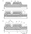
図1(A)に示すように、絶縁表面を有する基板50上にゲート電極51を形成する。絶縁表面を有する基板50は、バリウムホウケイ酸ガラス、アルミノホウケイ酸ガラス、若しくはアルミノシリケートガラスなど、フュージョン法やフロート法で作製される無アルカリガラス基板等を用いることができる。絶縁表面を有する基板50がマザーガラスの場合、基板の大きさは、第1世代(320mm×400mm)、第2世代(400mm×500mm)、第3世代(550mm×650mm)、第4世代(680mm×880mm、または730mm×920mm)、第5世代(1000mm×1200mmまたは1100mm×1250mm)、第6世代1500mm×1800mm)、第7世代(1900mm×2200mm)、第8世代(2160mm×2460mm)、第9世代(2400mm×2800mm、2450mm×3050mm)、第10世代(2950mm×3400mm)等を用いることができる。
As shown in FIG. 1A, a
ゲート電極51は、チタン、モリブデン、クロム、タンタル、タングステン、アルミニウムなどの金属材料またはその合金材料を用いて形成する。ゲート電極51は、スパッタリング法や真空蒸着法で絶縁表面を有する基板50上に導電膜を形成し、当該導電膜上にフォトリソグラフィ技術またはインクジェット法によりマスクを形成し、当該マスクを用いて導電膜をエッチングすることで、形成することができる。また、銀、金、銅などの導電性ナノペーストを用いてインクジェット法により吐出し焼成して、ゲート電極51を形成することもできる。なお、ゲート電極51の密着性向上と下地への拡散を防ぐバリアメタルとして、上記金属材料の窒化物膜を、絶縁表面を有する基板50及びゲート電極51の間に設けてもよい。ここでは、第1のフォトマスクを用いて形成したレジストマスクを用いて絶縁表面を有する基板50上に形成された導電膜をエッチングしてゲート電極を形成する。
The
具体的なゲート電極構造の例としては、アルミニウム膜上にモリブデン膜を積層させ、アルミニウム特有のヒロックやエレクトロマイグレーションを防ぐ構造にしてもよい。また、アルミニウム膜をモリブデン膜で挟んだ3層構造としてもよい。また、他のゲート電極構造の例として、銅膜上にモリブデン膜の積層、銅膜上に窒化チタン膜の積層、銅膜上に窒化タンタル膜の積層が挙げられる。 As a specific example of the gate electrode structure, a molybdenum film may be stacked on an aluminum film to prevent a hillock or electromigration peculiar to aluminum. Alternatively, a three-layer structure in which an aluminum film is sandwiched between molybdenum films may be used. As another example of the gate electrode structure, a molybdenum film is laminated on a copper film, a titanium nitride film is laminated on the copper film, and a tantalum nitride film is laminated on the copper film.
なお、ゲート電極51上には半導体膜や配線を形成するので、段切れ防止のため端部がテーパー状になるように加工することが望ましい。また、図示しないがこの工程でゲート電極に接続する配線も同時に形成することができる。
Note that since a semiconductor film or a wiring is formed over the
次に、ゲート電極51上に、ゲート絶縁膜52a、52b、52cを順に形成する。ここまでの工程を終えた断面図が図1(A)に相当する。
Next,
ゲート絶縁膜52a、52bはそれぞれ、プラズマCVD法やスパッタリング法等を用いて、酸化珪素膜、窒化珪素膜、酸化窒化珪素膜、または窒化酸化珪素膜で形成することができる。ゲート絶縁膜に形成されるピンホール等による層間ショートを防ぐため、異なる絶縁膜を用いて多層とすることが好ましい。そして、ゲート絶縁膜52cはYSZ膜で形成する。ここでは、ゲート絶縁膜52a、52b、52cとして、窒化珪素膜、酸化窒化珪素膜、YSZ膜の順に積層して形成する形態を示す。
Each of the
ここでは、酸化窒化珪素膜とは、その組成として、窒素よりも酸素の含有量が多いものであり、濃度範囲として酸素が55〜65原子%、窒素が1〜20原子%、Siが25〜35原子%、水素が0.1〜10原子%の範囲において、合計100原子%となるように各元素を任意の濃度で含むものをいう。また、窒化酸化珪素膜とは、その組成として、酸素よりも窒素の含有量が多いものであり、濃度範囲として酸素が15〜30原子%、窒素が20〜35原子%、Siが25〜35原子%、水素が15〜25原子%の範囲において、合計100原子%となるように各元素を任意の濃度で含むものをいう。 Here, the silicon oxynitride film has a composition that contains more oxygen than nitrogen, and the concentration ranges of oxygen are 55 to 65 atomic%, nitrogen is 1 to 20 atomic%, and Si is 25 to 25%. In the range of 35 atomic% and hydrogen in the range of 0.1 to 10 atomic%, it means that each element is contained at an arbitrary concentration so that the total is 100 atomic%. The silicon nitride oxide film has a nitrogen content higher than that of oxygen as a composition. The concentration ranges of oxygen are 15 to 30 atomic%, nitrogen is 20 to 35 atomic%, and Si is 25 to 35. In the range of atomic% and hydrogen in the range of 15 to 25 atomic%, it means that each element is contained at an arbitrary concentration so that the total is 100 atomic%.
ゲート絶縁膜52a及びゲート絶縁膜52bの膜厚はともに50nmよりも厚くする。ゲート絶縁膜52aは、基板からの不純物(例えばアルカリ金属など)の拡散を防ぐために、窒化珪素膜または窒化酸化珪素膜とすることが好ましい。また、ゲート絶縁膜52aは、ゲート電極の酸化防止の他、ゲート電極にアルミニウムを用いる場合にはヒロックを防止することができる。
Both the
ゲート絶縁膜52a及びゲート絶縁膜52bは、周波数が1GHzのマイクロ波を導入できる、マイクロ波プラズマCVD装置を用いて形成してもよい。マイクロ波プラズマCVD装置で形成した酸化窒化珪素膜、窒化酸化珪素膜は、耐圧が高く、薄膜トランジスタの信頼性を高めることができる。
The
ゲート絶縁膜52cとして、YSZ膜を成膜する。このときイットリアとジルコニアを8mol%:92mol%にて混合したターゲットを用いて、スパッタ法にて、成膜ガスをアルゴン(Ar)及び酸素(O2)、成膜圧力0.4Paとして、10〜200nm、具体的には50nmの膜厚で成膜する(図1(A)参照)。尚、成膜時の基板温度は高いほど良いが、本発明においては室温でも良い。またYSZ膜中にイットリアは、20mol%以下の範囲で含まれるものとする。
A YSZ film is formed as the
YSZ膜は、耐熱性、化学的安定性に優れ、また特定の面方位に結晶成長しやすい特徴がある。YSZ膜の比誘電率は20程度であり、結晶化するほど比誘電率が向上する。また絶縁物である。ガラスの耐熱温度の範囲では結晶性は大きく変わらないので、成膜時基板温度は、室温からガラスの耐熱温度範囲内の何れでも適している。 The YSZ film is excellent in heat resistance and chemical stability, and has a feature that crystal growth is easy in a specific plane orientation. The relative dielectric constant of the YSZ film is about 20, and the relative dielectric constant improves as it crystallizes. It is also an insulator. Since the crystallinity does not change greatly in the range of the heat resistant temperature of glass, the substrate temperature during film formation is suitable in any range from room temperature to the heat resistant temperature range of glass.
ここでは、ゲート絶縁膜を3層構造としたが、例えば液晶表示装置のスイッチング素子に用いる場合、交流駆動させるため、図5(A)のように酸化珪素膜、窒化珪素膜、酸化窒化珪素膜、または窒化酸化珪素膜の何れかを第1層目のゲート絶縁膜52aとし、YSZ膜を第2層目のゲート絶縁膜52cとした積層構造とするか、図5(B)のようにYSZ膜の単層のゲート絶縁膜52cとしてもよい。
Although the gate insulating film has a three-layer structure here, for example, when used for a switching element of a liquid crystal display device, a silicon oxide film, a silicon nitride film, and a silicon oxynitride film are used as shown in FIG. Or a silicon nitride oxide film as a first
ここでYSZ膜表面を活性化し、上層に成膜される膜をYSZ膜の結晶性に影響されやすくするため、表面をプラズマ処理しても良い。プラズマ処理には、H2、O2、Ar、N2、から選ばれた一、あるいはこれらの組み合わせを用いればよいが、ここでは逆スパッタリング法によるArプラズマ処理を行う。YSZ膜成膜後、Arガス雰囲気で、圧力0.2Paにおいて基板がカソードとなるように電圧を印加し、YSZ膜が消失しない条件範囲にて、逆スパッタリング処理を行う。 Here, in order to activate the surface of the YSZ film and make the film formed as an upper layer easily affected by the crystallinity of the YSZ film, the surface may be subjected to plasma treatment. For the plasma treatment, one selected from H 2 , O 2 , Ar, N 2 , or a combination thereof may be used. Here, Ar plasma treatment by reverse sputtering is performed. After forming the YSZ film, a voltage is applied in an Ar gas atmosphere so that the substrate becomes a cathode at a pressure of 0.2 Pa, and reverse sputtering is performed in a condition range in which the YSZ film does not disappear.
次いで、ゲート絶縁膜の成膜後、図1(B)のように微結晶半導体膜53を成膜する。微結晶半導体膜53は、非晶質と結晶構造(単結晶、多結晶を含む)の中間的な構造の半導体を含む膜である。この半導体は、自由エネルギー的に安定な第3の状態を有する半導体であって、短距離秩序を持ち格子歪みを有する結晶質なものであり、その膜表面より見た粒径が0.5〜20nmの柱状または針状結晶が基板表面に対して法線方向に成長している。また、微結晶半導体と非晶質半導体とが混在している。微結晶半導体の代表例である微結晶シリコンは、そのラマンスペクトルが単結晶シリコンを示す520cm−1よりも低波数側に、シフトしている。即ち、単結晶シリコンを示す520cm−1とアモルファスシリコンを示す480cm−1の間に微結晶シリコンのラマンスペクトルのピークがある。また、未結合手(ダングリングボンド)を終端するため水素またはハロゲンを少なくとも1原子%またはそれ以上含ませている。さらに、ヘリウム、アルゴン、クリプトン、ネオンなどの希ガス元素を含ませて格子歪みをさらに助長させることで、安定性が増し良好な微結晶半導体膜が得られる。このような微結晶半導体膜に関する記述は、例えば、米国特許4,409,134号で開示されている。
Next, after forming the gate insulating film, a
この微結晶半導体膜は、周波数が数十MHz〜数百MHzの高周波プラズマCVD装置、または周波数が1GHz以上のマイクロ波プラズマCVD装置により形成することができる。代表的には、SiH4、Si2H6、SiH2Cl2、SiHCl3、SiCl4、SiF4などの水素化珪素またはハロゲン化珪素を水素で希釈して形成することができる。また、これらに加え、ヘリウム、アルゴン、クリプトン、ネオンから選ばれた一種または複数種の希ガス元素で希釈して微結晶半導体膜を形成することができる。これらのときの水素化珪素またはハロゲン化珪素に対して水素の流量を5倍以上200倍以下、好ましくは50倍以上150倍以下、更に好ましくは100倍とする。 This microcrystalline semiconductor film can be formed by a high-frequency plasma CVD apparatus having a frequency of several tens to several hundreds of MHz or a microwave plasma CVD apparatus having a frequency of 1 GHz or more. Typically, it can be formed by diluting silicon hydride or silicon halide such as SiH 4 , Si 2 H 6 , SiH 2 Cl 2 , SiHCl 3 , SiCl 4 , or SiF 4 with hydrogen. In addition to these, a microcrystalline semiconductor film can be formed by diluting with one or more kinds of rare gas elements selected from helium, argon, krypton, and neon. The flow rate of hydrogen is 5 to 200 times, preferably 50 to 150 times, more preferably 100 times that of silicon hydride or silicon halide.
また、上記のプラズマCVD成膜ガスにゲルマン(GeH4)等を加えると、シリコン固有の結晶構造を保持しつつ、シリコンの一部がゲルマニウムに置換された構造が形成される。これにより、形成される結晶の格子定数を小さくすることができる。そのため、形成されるシリコン固有の結晶構造の格子定数の値をYSZの格子定数の値に近づけることができ、微結晶半導体膜の結晶化を促進することができる。 Further, when germane (GeH 4 ) or the like is added to the plasma CVD film forming gas, a structure in which part of silicon is replaced with germanium is formed while maintaining a crystal structure unique to silicon. Thereby, the lattice constant of the formed crystal can be reduced. Therefore, the value of the lattice constant of the crystal structure unique to silicon to be formed can be made close to the value of the lattice constant of YSZ, and crystallization of the microcrystalline semiconductor film can be promoted.
また、微結晶半導体膜は、価電子制御を目的とした不純物元素を意図的に添加しないときに弱いn型の電気伝導性を示すので、薄膜トランジスタのチャネル形成領域として機能する微結晶半導体膜に対しては、p型を付与する不純物元素を、成膜と同時に、或いは成膜後に添加することで、しきい値制御をすることが可能となる。p型を付与する不純物元素としては、代表的には硼素であり、B2H6、BF3などの不純物気体を1ppm〜1000ppm、好ましくは1〜100ppmの割合で水素化珪素に混入させると良い。そしてボロンの濃度を、例えば1×10¹⁴〜6×10¹⁶atoms/cm3とすると良い。 In addition, since the microcrystalline semiconductor film exhibits weak n-type conductivity when an impurity element for the purpose of controlling valence electrons is not intentionally added, the microcrystalline semiconductor film functions as a channel formation region of a thin film transistor. Thus, the threshold value can be controlled by adding an impurity element imparting p-type at the same time as film formation or after film formation. The impurity element imparting p-type is typically boron, and an impurity gas such as B 2 H 6 or BF 3 may be mixed into silicon hydride at a rate of 1 ppm to 1000 ppm, preferably 1 to 100 ppm. . The boron concentration is preferably 1 × 10 14 to 6 × 10 16 atoms / cm 3 , for example.
また、微結晶半導体膜の酸素濃度を、5×10¹⁹atoms/cm3以下、より好ましくは1×1019atoms/cm3以下、窒素及び炭素の濃度をそれぞれ1×1018atoms/cm3以下とすることが好ましい。酸素、窒素、及び炭素が微結晶半導体膜に混入する濃度を低減することで、微結晶半導体膜がn型化することを防止することができる。 Further, the oxygen concentration of the microcrystalline semiconductor film is 5 × 10 19 atoms / cm 3 or less, more preferably 1 × 10 19 atoms / cm 3 or less, and the concentrations of nitrogen and carbon are 1 × 10 18 atoms / cm 3 or less, respectively. It is preferable that By reducing the concentration of oxygen, nitrogen, and carbon mixed in the microcrystalline semiconductor film, the microcrystalline semiconductor film can be prevented from becoming n-type.
微結晶半導体膜53は、0nmより厚く50nm以下、好ましくは0nmより厚く20nm以下で形成する。
The
このとき図6(A)のように、結晶性の良いYSZ膜で形成されるゲート絶縁膜52cの上に形成された微結晶半導体膜53は、ゲート絶縁膜であるYSZ膜との界面付近ではYSZ膜の結晶構造に影響を受けるため、図6(B)のように結晶性が高まっている。
At this time, as shown in FIG. 6A, the
微結晶半導体膜53は後に形成される薄膜トランジスタのチャネル形成領域として機能する。微結晶半導体膜53の厚さを上記の範囲内とすることで、後に形成される薄膜トランジスタは、完全空乏型となる。また、微結晶半導体膜は微結晶で構成されているため、非晶質半導体膜と比較して抵抗が低い。このため、微結晶半導体膜を用いた薄膜トランジスタは、電流電圧特性を示す曲線の立ち上がり部分の傾きが急峻となり、スイッチング素子としての応答性が優れ、高速動作が可能となる。また、薄膜トランジスタのチャネル形成領域に微結晶半導体膜を用いることで、薄膜トランジスタのしきい値の変動を抑制することが可能である。このため、電気特性のばらつきの少ない液晶表示装置を作製することができる。
The
また、微結晶半導体膜は非晶質半導体膜と比較して移動度が高い。このため、表示装置のスイッチング素子として、チャネル形成領域が微結晶半導体膜で形成される薄膜トランジスタを用いることで、薄膜トランジスタの面積を縮小することが可能である。このため、一画素あたりに示す薄膜トランジスタの面積が小さくなり、画素の開口率を高めることが可能である。この結果、解像度の高い表示装置を作製することができる。 In addition, the microcrystalline semiconductor film has higher mobility than the amorphous semiconductor film. Therefore, by using a thin film transistor in which a channel formation region is formed using a microcrystalline semiconductor film as a switching element of the display device, the area of the thin film transistor can be reduced. Therefore, the area of the thin film transistor shown per pixel is reduced, and the aperture ratio of the pixel can be increased. As a result, a display device with high resolution can be manufactured.
次いで、微結晶半導体膜53の成膜後、バッファ層54を成膜する。バッファ層54は、水素、窒素、若しくはハロゲンを含む非晶質半導体膜を用いて形成する。水素化珪素の流量の1倍以上10倍以下、更に好ましくは1倍以上5倍以下の流量の水素を用いて、水素を含む非晶質半導体膜を形成することができる。また、上記水素化珪素と窒素またはアンモニアとを用いることで、窒素を含む非晶質半導体膜を形成することができる。また、上記水素化珪素と、フッ素、又は塩素を含む気体(F2、Cl2、HF、HCl等)を用いることで、フッ素、又は塩素を含む非晶質半導体膜を形成することができる。なお、水素化珪素の代わりに、SiH2Cl2、SiHCl3、SiCl4、SiF4等を用いることができる。
Next, after the
また、バッファ層54は、ターゲットに非晶質半導体を用いて水素、または希ガスでスパッタリングして形成することができる。このとき、アンモニア、窒素、またはN2Oを雰囲気中に含ませることにより、窒素を含む非晶質半導体膜を形成することができる。また、雰囲気中にフッ素、又は塩素を含む気体(F2、Cl2、HF、HCl等)を含ませることにより、フッ素、又は塩素を含む非晶質半導体膜を形成することができる。
The
バッファ層54は、結晶粒を含まない非晶質半導体膜で形成することが好ましい。このため、周波数が数十MHz〜数百MHzの高周波プラズマCVD装置、またはマイクロ波プラズマCVD装置で形成する場合は、結晶粒を含まない非晶質半導体膜となるように、成膜条件を制御することが好ましい。
The
バッファ層54は、後のソース領域及びドレイン領域の形成プロセスにおいて、一部エッチングされる。そのときに、微結晶半導体膜53が露呈しないようにバッファ層54の一部が残存する厚さで形成することが好ましい。代表的には、50nm以上400nm以下、好ましくは80nm以上300nm以下の厚さで形成することが好ましい。薄膜トランジスタの印加電圧の高い(例えば15V程度)表示装置、代表的には液晶表示装置において、バッファ層54の膜厚を上記範囲に示すように厚く形成すると、耐圧が高くなり、薄膜トランジスタに高い電圧が印加されても、薄膜トランジスタが劣化することを回避することができる。
The
なお、バッファ層54には、リンやボロン等の一導電型を付与する不純物元素が添加されていない。後に成膜される一導電型を付与する不純物元素が添加された半導体膜55から不純物元素が微結晶半導体膜53へ拡散しないように、バッファ層54がバリア層として機能している。バッファ層を設けない場合も可であるが、微結晶半導体膜53と一導電型を付与する不純物元素が添加された半導体膜55とが接してしまう場合、後のエッチング工程や加熱処理により不純物元素が移動し、しきい値制御が困難になる恐れがある。
Note that an impurity element imparting one conductivity type, such as phosphorus or boron, is not added to the
さらにバッファ層54を微結晶半導体膜53の表面上に形成することで、微結晶半導体膜53に含まれる結晶粒の表面の自然酸化を防止することが可能である。特に、非晶質半導体と微結晶粒が接する領域では、局部応力により亀裂が入りやすい。この亀裂が酸素に触れると結晶粒は酸化され、酸化珪素が形成されてしまう。
Further, by forming the
非晶質半導体膜であるバッファ層54のエネルギーギャップは微結晶半導体膜53に比べて大きく(非晶質半導体膜のエネルギーギャップは1.6〜1.8eV、微結晶半導体膜53のエネルギーギャップは1.1〜1.5eV)、また移動度は微結晶半導体膜53と比較し1/5〜1/10程度と低くなるため抵抗が高い。このため、後に形成される薄膜トランジスタにおいて、ソース領域及びドレイン領域と、微結晶半導体膜53との間に形成されるバッファ層は高抵抗領域として機能し、微結晶半導体膜53がチャネル形成領域として機能する。この抵抗値の高さが理由の一となり、薄膜トランジスタのオフ電流を低減することができる。そのため、当該薄膜トランジスタを表示装置のスイッチング素子として用いた場合、表示装置のコントラストを向上させることができる。
The energy gap of the
なお、微結晶半導体膜53上に、プラズマCVD法によりバッファ層54を300℃〜400℃の温度にて成膜することが好ましい。この成膜処理により水素が微結晶半導体膜53に供給され、微結晶半導体膜53を水素化したのと同等の効果が得られる。すなわち、微結晶半導体膜53上にバッファ層54を堆積することにより、微結晶半導体膜53に水素を拡散させて、ダングリングボンドの終端を行うことができる。
Note that the
次いで、バッファ層54の成膜後、大気に触れさせることなく基板を搬送し、バッファ層54を成膜する反応室とは異なる反応室で、一導電型を付与する不純物元素が添加された半導体膜55を成膜することが好ましい。この段階での断面図が図1(C)に相当する。バッファ層54を成膜する反応室とは異なる反応室で、一導電型を付与する不純物元素が添加された半導体膜55を成膜することでバッファ層の成膜時に一導電型を付与する不純物元素が混入しないようにすることができる。
Next, after the
一導電型を付与する不純物元素が添加された半導体膜55は、nチャネル型の薄膜トランジスタを形成する場合には、代表的な不純物元素としてリンを添加すれば良く、水素化珪素にフォスフィンガス(PH3)などの不純物気体を加えれば良い。また、pチャネル型の薄膜トランジスタを形成する場合には、代表的な不純物元素としてボロンを添加すれば良く、水素化珪素にB2H6などの不純物気体を加えれば良い。一導電型を付与する不純物元素が添加された半導体膜55は、微結晶半導体、または非晶質半導体で形成することができる。一導電型を付与する不純物元素が添加された半導体膜55は2nm以上50nm以下の厚さで形成する。一導電型を付与する不純物元素が添加された半導体膜の膜厚を、薄くすることでスループットを向上させることができる。
In the case of forming an n-channel thin film transistor, the
次いで、図2(A)に示すように、一導電型を付与する不純物元素が添加された半導体膜55上にレジストマスク56を形成する。レジストマスク56は、フォトリソグラフィ技術またはインクジェット法により形成する。ここでは、第2のフォトマスクを用いて、一導電型を付与する不純物元素が添加された半導体膜55上に塗布されたレジストを露光現像して、レジストマスク56を形成する。
Next, as illustrated in FIG. 2A, a resist
次いで、レジストマスク56を用いて微結晶半導体膜53、バッファ層54、及び一導電型を付与する不純物元素が添加された半導体膜55をエッチングし、島状にして、図2(B)に示すように、島状の微結晶半導体膜61、島状のバッファ層62、及び島状の一導電型を付与する不純物元素が添加された半導体膜63を形成する。この後、レジストマスク56を除去する。
Next, the
島状の微結晶半導体膜61、島状のバッファ層62の端部側面が傾斜していることにより、島状のバッファ層62上に形成されるソース領域及びドレイン領域と島状の微結晶半導体膜61との間にリーク電流が生じることを防止することが可能である。島状の微結晶半導体膜61及び島状のバッファ層62の端部側面の傾斜角度は、30°〜90°、好ましくは45°〜80°である。このような角度とすることで、段差形状によるソース電極またはドレイン電極の段切れを防ぐことができる。
The source and drain regions formed on the island-shaped
次に、図2(C)に示すように、島状の一導電型を付与する不純物元素が添加された半導体膜63及びゲート絶縁膜52c上に導電膜65a、65b、65cを形成する。導電膜65a、65b、65cは、アルミニウム、若しくは銅、シリコン、チタン、ネオジム、スカンジウム、モリブデンなどの耐熱性向上元素若しくはヒロック防止元素が添加されたアルミニウム合金の単層または積層で形成することが好ましい。また、一導電型を付与する不純物元素が添加された半導体膜と接する側の膜を、チタン、タンタル、モリブデン、タングステン、またはこれらの元素の窒化物で形成し、その上にアルミニウムまたはアルミニウム合金を形成した積層構造としても良い。更には、アルミニウムまたはアルミニウム合金の上面及び下面を、チタン、タンタル、モリブデン、タングステン、またはこれらの元素の窒化物で挟んだ積層構造としてもよい。ここでは、導電膜としては、導電膜65a、65b、65c3層が積層した構造の導電膜を示し、導電膜65a、65cにモリブデン膜、導電膜65bにアルミニウム膜を用いた積層導電膜や、導電膜65a、65cにチタン膜、導電膜65bにアルミニウム膜を用いた積層導電膜を示す。導電膜65a、65b、65cは、スパッタリング法や真空蒸着法で形成する。
Next, as illustrated in FIG. 2C,
次に、図2(D)に示すように、導電膜65a、65b、65c上に第3のフォトマスクを用いてレジストマスク66を形成し、導電膜65a、65b、65cの一部をエッチングしてソース電極及びドレイン電極の一方71a、71b、71c、並びにソース電極及びドレイン電極の他方71d、71e、71fを形成する。また、ウエットエッチングを行うことにより、レジストマスク66より面積の小さいソース電極及びドレイン電極の一方71a、71b、71c、並びにソース電極及びドレイン電極の他方71d、71e、71fを形成することができる。
Next, as illustrated in FIG. 2D, a resist
次に、図3(A)に示すように、レジストマスク66を用いて島状の一導電型を付与する不純物元素が添加された半導体膜63をエッチングして、ソース領域及びドレイン領域の一方72a、並びにソース領域及びドレイン領域の他方72bを形成する。さらに、当該エッチング工程において、島状のバッファ層62の一部もエッチングされる。一部エッチングされた、凹部が形成されたバッファ層をバッファ層73と示す。ソース領域及びドレイン領域の形成工程と、バッファ層の凹部とを同一工程で形成することができる。バッファ層の凹部の深さをバッファ層の一番膜厚の厚い領域の1/2〜1/3とすることで、ソース領域及びドレイン領域の距離を離すことが可能であるため、ソース領域及びドレイン領域の間でのリーク電流を低減することができる。この後、レジストマスク66を除去する。
Next, as illustrated in FIG. 3A, the resist
次に、図3(B)に示すように、ソース電極及びドレイン電極の一方71a、71b、71c、ソース電極及びドレイン電極の他方71d、71e、71f、ソース領域及びドレイン領域の一方72a、ソース領域及びドレイン領域の他方72b、並びにバッファ層73を覆う絶縁膜76を形成する。絶縁膜76は、ゲート絶縁膜52a、52b、52cと同じ成膜方法を用いて形成することができる。なお、絶縁膜76は、大気中に浮遊する有機物や金属物、水蒸気などの汚染不純物の侵入を防ぐためのものであり、緻密な膜が好ましい。また、絶縁膜76に窒化珪素膜を用いることで、島状のバッファ層62中の酸素濃度を5×10¹⁹atoms/cm3以下、好ましくは1×1019atoms/cm3以下とすることができる。
Next, as shown in FIG. 3B, one of the source and
図3(B)に示すように、ソース電極及びドレイン電極の一方71a、71b、71cの端部とソース領域及びドレイン領域の一方72a、並びにソース電極及びドレイン電極の他方71d、71e、71fとソース領域及びドレイン領域の他方72bの端部は、それぞれ一致せずずれた形状となることで、ソース電極及びドレイン電極の端部の距離が離れるため、ソース電極及びドレイン電極間のリーク電流やショートを防止することができる。また、ソース電極及びドレイン電極、並びにソース領域及びドレイン領域の端部に電界が集中せず、ゲート電極51と、ソース電極又はドレイン電極との間でのリーク電流を防止することができる。このため、信頼性が高く、且つ耐圧の高い薄膜トランジスタを作製することができる。
As shown in FIG. 3B, the ends of one of the source and
以上の工程により、薄膜トランジスタ74を形成することができる。
Through the above process, the
本実施の形態で示す薄膜トランジスタは、ゲート電極上にゲート絶縁膜、微結晶半導体膜、バッファ層、ソース領域及びドレイン領域、ソース電極及びドレイン電極が積層され、チャネル形成領域として機能する微結晶半導体膜の表面をバッファ層が覆う。また、バッファ層の一部には凹部が形成されており、当該凹部以外の領域がソース領域及びドレイン領域で覆われる。即ち、バッファ層に形成される凹部により、ソース領域及びドレイン領域の距離が離れているため、ソース領域及びドレイン領域の間でのリーク電流を低減することができる。また、バッファ層の一部がエッチングされ凹部を形成することにより、ソース領域及びドレイン領域の形成工程において発生するエッチング残渣を除去することができるため、残渣を介してソース領域及びドレイン領域にリーク電流(寄生チャネル)が発生することを回避することができる。 In the thin film transistor described in this embodiment, a gate insulating film, a microcrystalline semiconductor film, a buffer layer, a source region and a drain region, a source electrode and a drain electrode are stacked over a gate electrode, and the microcrystalline semiconductor film functions as a channel formation region A buffer layer covers the surface. In addition, a recess is formed in a part of the buffer layer, and a region other than the recess is covered with the source region and the drain region. That is, since the distance between the source region and the drain region is separated by the recess formed in the buffer layer, the leakage current between the source region and the drain region can be reduced. In addition, since a part of the buffer layer is etched to form a recess, an etching residue generated in the process of forming the source region and the drain region can be removed, so that a leakage current flows into the source region and the drain region through the residue. Generation of (parasitic channel) can be avoided.
また、チャネル形成領域として機能する微結晶半導体膜とソース領域及びドレイン領域との間に、バッファ層が形成されている。また、微結晶半導体膜の表面がバッファ層で覆われている。高抵抗のバッファ層は、微結晶半導体膜と、ソース領域及びドレイン領域との間にまで延在しているため、薄膜トランジスタにリーク電流が発生することを低減することができると共に、高い電圧の印加による劣化を低減することができる。また、バッファ層と、微結晶半導体膜と、ソース領域及びドレイン領域は、ゲート電極と重畳する領域上に形成される。従って、ゲート電極の端部形状に影響されない構造と言える。ゲート電極を積層構造とした場合、下層としてアルミニウムを用いると、ゲート電極側面にアルミニウムが露出し、ヒロックが発生する恐れがあるが、さらにソース領域及びドレイン領域をゲート電極端部とも重ならない構成とすることで、ゲート電極側面と重なる領域でショートが発生することを防ぐことができる。また、微結晶半導体膜の表面に水素で表面が終端された非晶質半導体膜がバッファ層として形成されているため、微結晶半導体膜の酸化を防止することが可能であると共に、ソース領域及びドレイン領域の形成工程に発生するエッチング残渣が微結晶半導体膜に混入することを防ぐことができる。このため、電気特性が優れ、且つ耐圧に優れた薄膜トランジスタである。 In addition, a buffer layer is formed between the microcrystalline semiconductor film functioning as a channel formation region and the source and drain regions. In addition, the surface of the microcrystalline semiconductor film is covered with a buffer layer. Since the high-resistance buffer layer extends between the microcrystalline semiconductor film and the source and drain regions, leakage current can be reduced in the thin film transistor and high voltage can be applied. It is possible to reduce deterioration due to. The buffer layer, the microcrystalline semiconductor film, the source region, and the drain region are formed over a region overlapping with the gate electrode. Therefore, it can be said that the structure is not affected by the end shape of the gate electrode. When the gate electrode has a laminated structure, if aluminum is used as the lower layer, aluminum may be exposed on the side surface of the gate electrode and hillocks may be generated, but the source region and the drain region do not overlap the gate electrode end. By doing so, it is possible to prevent a short circuit from occurring in a region overlapping with the side surface of the gate electrode. Further, since the amorphous semiconductor film whose surface is terminated with hydrogen is formed as a buffer layer on the surface of the microcrystalline semiconductor film, the microcrystalline semiconductor film can be prevented from being oxidized, and the source region and Etching residues generated in the drain region formation step can be prevented from entering the microcrystalline semiconductor film. Therefore, the thin film transistor has excellent electrical characteristics and excellent withstand voltage.
また、薄膜トランジスタのチャネル長を短くすることができ、薄膜トランジスタの平面面積を縮小することができる。 In addition, the channel length of the thin film transistor can be shortened, and the planar area of the thin film transistor can be reduced.
次に、絶縁膜76に第4のフォトマスクを用いて形成したレジストマスクを用いて、絶縁膜76の一部をエッチングしてコンタクトホールを形成し、当該コンタクトホールにおいてソース電極及びドレイン電極の他方71fに接する画素電極77を形成する。
Next, a contact hole is formed by etching part of the insulating
図4に示すように、ソース領域及びドレイン領域の一方72a、並びにソース領域及びドレイン領域の他方72bの端部は、それぞれソース電極及びドレイン電極の一方71c、並びにソース電極及びドレイン電極の他方71fの端部の外側に位置することが分かる。また、バッファ層73の端部はソース領域及びドレイン領域の一方72a、並びにソース領域及びドレイン領域の他方72bの端部の外側に位置する。また、ソース領域及びドレイン領域の一方72aはソース領域及びドレイン領域の他方72bを囲む形状(具体的には、U字型、C字型)である。このため、キャリアが移動する領域の面積を増加させることが可能であるため、電流量を増やすことが可能であり、薄膜トランジスタの面積を縮小することができる。また、ゲート電極上において、微結晶半導体膜、ソース電極及びドレイン電極が重畳されているため、ゲート電極の凹凸の影響が少なく、被覆率の低減及びリーク電流の発生を抑制することができる。なお、図4の鎖線A−Bの断面は図3(c)の断面図が相当する。
As shown in FIG. 4, one
また、画素電極77は、酸化タングステンを含むインジウム酸化物、酸化タングステンを含むインジウム亜鉛酸化物、酸化チタンを含むインジウム酸化物、酸化チタンを含むインジウム錫酸化物、インジウム錫酸化物、インジウム亜鉛酸化物、酸化ケイ素を添加したインジウム錫酸化物などの透光性を有する導電性材料を用いることができる。
The
また、画素電極77として、導電性高分子(導電性ポリマーともいう)を含む導電性組成物を用いて形成することができる。導電性組成物を用いて形成した画素電極は、シート抵抗が10000Ω/□以下、波長550nmにおける透光率が70%以上であることが好ましい。また、導電性組成物に含まれる導電性高分子の抵抗率が0.1Ω・cm以下であることが好ましい。
The
導電性高分子としては、いわゆるπ電子共役系導電性高分子を用いることができる。例えば、ポリアニリンまたはその誘導体、ポリピロールまたはその誘導体、ポリチオフェンまたはその誘導体、若しくはこれらの2種以上の共重合体などがあげられる。 As the conductive polymer, a so-called π-electron conjugated conductive polymer can be used. For example, polyaniline or a derivative thereof, polypyrrole or a derivative thereof, polythiophene or a derivative thereof, or a copolymer of two or more kinds thereof can be given.
ここでは、画素電極77としては、スパッタリング法によりインジウム錫酸化物膜を成膜した後、インジウム錫酸化物膜上にレジストを塗布する。次に、第5のフォトマスクを用いてレジストを露光及び現像し、レジストマスクを形成する。次に、レジストマスクを用いてインジウム錫酸化物膜をエッチングして画素電極77を形成する。
Here, as the
以上によりYSZ膜を下地として微結晶半導体膜の結晶性が高められ、電界効果移動度の高い薄膜トランジスタを用いた、表示装置に適用可能な素子基板を形成することができる。 Through the above steps, an element substrate that can be used for a display device using a thin film transistor with high field-effect mobility can be formed using the YSZ film as a base to improve the crystallinity of the microcrystalline semiconductor film.
(実施の形態2)
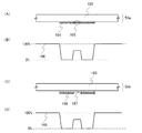
実施の形態1では、ゲート絶縁膜として成膜されたYSZ膜上に、微結晶半導体膜を単層で形成したが、微結晶半導体膜をYSZと格子定数の近いシリコンにて形成するのであれば、どのような微結晶半導体膜の形成方法でも有効である。実施の形態2では、さらに成膜初期に形成される半導体領域の品質を向上するため、ゲート電極上にゲート絶縁膜を形成した後、成膜速度は低いが品質のよい第1の成膜条件でゲート絶縁膜界面付近の微結晶半導体膜を成膜し、その後、高い成膜速度の第2の成膜条件に変えて微結晶半導体膜を成膜する。成膜速度を高くする方法は段階的でも連続的でも良い。以下にその方法を説明する。
(Embodiment 2)
In
成膜速度は低いが品質のよい第1の成膜条件としては、予め成膜前に真空チャンバー(反応室)内の酸素や窒素、H2Oなどのガスの残留を極力低減するため、到達最低圧力を1×10⁻⁷〜1×10⁻¹⁰Torr(約1×10⁻⁵Pa以上1×10⁻⁸Pa)の超高真空(UHV)領域に下げ、高い純度の材料ガスを流し、成膜時の基板温度を100℃以上300℃未満の範囲とする。 The first film formation condition with low film formation speed but good quality is reached in order to reduce the residual of oxygen, nitrogen, H 2 O and other gases in the vacuum chamber (reaction chamber) as much as possible before film formation. The minimum pressure is lowered to an ultra high vacuum (UHV) region of 1 × 10 −7 to 1 × 10 −10 Torr (about 1 × 10 −5 Pa or more and 1 × 10 −8 Pa), and a high purity material gas is flowed. The substrate temperature during film formation is set to a range of 100 ° C. or higher and lower than 300 ° C.
また、第2の成膜条件としては、少なくとも第1の成膜条件の成膜速度よりも速い成膜速度が得られる条件とすればよく、例えば、シランガスと水素ガスの流量比を第1の成膜条件とは変えて微結晶半導体膜が形成される範囲内で水素濃度を下げればよい。また、第2の成膜条件としては、第1の成膜条件の基板温度よりも高い温度、例えば300℃以上の基板温度として成膜速度を速くしてもよい。また、第2の成膜条件として、第1の成膜条件よりも電力を増大させることにより、成膜速度を速くしてもよい。また、反応室のコンダクタンスバルブなどの排気バルブを調節して第2の成膜条件を第1の成膜条件と異なる真空度として成膜速度を速くしてもよい。 The second film formation condition may be a condition that at least a film formation speed higher than the film formation speed of the first film formation condition may be obtained. For example, the flow rate ratio of silane gas and hydrogen gas is set to the first film formation speed. The hydrogen concentration may be lowered within the range in which the microcrystalline semiconductor film is formed instead of the deposition conditions. Further, as the second film formation condition, the film formation rate may be increased by setting the temperature higher than the substrate temperature of the first film formation condition, for example, a substrate temperature of 300 ° C. or higher. Further, as the second film formation condition, the film formation rate may be increased by increasing the electric power as compared with the first film formation condition. In addition, the deposition rate may be increased by adjusting the exhaust valve such as the conductance valve of the reaction chamber so that the second deposition condition is a vacuum different from the first deposition condition.
また、成膜初期の第1の成膜条件から成膜後期の高い成膜速度の第2の成膜条件に変えても、先に微結晶が形成されているため、それを核として品質の高い微結晶半導体膜を堆積することができる。また、予め、微結晶を形成しておくことにより成膜速度を速くすることができる。 Even if the first film formation condition at the initial stage of film formation is changed to the second film formation condition at a high film formation speed at the later stage of film formation, since microcrystals are formed first, A high microcrystalline semiconductor film can be deposited. In addition, the deposition rate can be increased by forming microcrystals in advance.
実施の形態1のように、YSZ膜を最上層としたゲート絶縁膜まで形成された構造の断面図を図7(A)に示す。この後上記のような方法にて、微結晶半導体膜を形成する成膜処理を行う。本実施の形態では、成膜速度は低いが品質のよい第1の成膜条件でゲート絶縁膜界面付近の膜を形成し、その後、高い成膜速度の第2の成膜条件に変えて膜を堆積する。 FIG. 7A shows a cross-sectional view of the structure in which the gate insulating film having the YSZ film as the uppermost layer is formed as in the first embodiment. Thereafter, a film formation process for forming a microcrystalline semiconductor film is performed by the above-described method. In this embodiment, a film in the vicinity of the gate insulating film interface is formed under a first film formation condition with a low film formation speed but good quality, and then changed to a second film formation condition with a high film formation speed. To deposit.
第1の成膜条件での成膜速度よりも第2の成膜条件の成膜速度が速ければ、成膜条件自体は特に限定されない。従って、周波数が数十MHz〜数百MHzの高周波プラズマCVD装置、または周波数が1GHz以上のマイクロ波プラズマCVD装置により形成し、代表的には、シラン(SiH4)、ジシラン(Si2H6)などの水素化珪素を水素で希釈してプラズマ生成することで成膜することができる。また、水素化珪素及び水素に加え、ヘリウム、アルゴン、クリプトン、ネオンから選ばれた一種または複数種の希ガス元素で希釈して微結晶半導体膜を形成することができる。なお、水素化珪素の代わりに、SiH2Cl2、SiHCl3、SiCl4、SiF4等を用いることもできる。 As long as the film formation speed under the second film formation condition is higher than the film formation speed under the first film formation condition, the film formation condition itself is not particularly limited. Therefore, it is formed by a high-frequency plasma CVD apparatus having a frequency of several tens of MHz to several hundreds of MHz, or a microwave plasma CVD apparatus having a frequency of 1 GHz or more, and is typically silane (SiH 4 ) or disilane (Si 2 H 6 ). A film can be formed by diluting silicon hydride such as hydrogen with hydrogen to generate plasma. In addition to silicon hydride and hydrogen, the microcrystalline semiconductor film can be formed by dilution with one or more kinds of rare gas elements selected from helium, argon, krypton, and neon. Note that SiH 2 Cl 2 , SiHCl 3 , SiCl 4 , SiF 4, or the like can be used instead of silicon hydride.
また、材料ガスにヘリウムを加えた場合、ヘリウムは24.5eVとすべての気体中で最も高いイオン化エネルギーを持ち、そのイオン化エネルギーよりも少し低い、約20eVの準位に準安定状態があるので、放電持続中においては、イオン化にはその差約4eVしか必要としない。そのため放電開始電圧も全ての気体中最も低い値を示す。このような特性から、ヘリウムはプラズマを安定的に維持することができる。また、均一なプラズマを形成することができるので、微結晶半導体膜を堆積する基板の面積が大きくなってもプラズマ密度の均一化を図る効果を奏する。 In addition, when helium is added to the material gas, helium has the highest ionization energy of all gases at 24.5 eV, and has a metastable state at a level of about 20 eV, which is slightly lower than the ionization energy. During the discharge duration, the difference requires only about 4 eV for ionization. Therefore, the discharge start voltage also shows the lowest value among all gases. From such characteristics, helium can maintain the plasma stably. In addition, since uniform plasma can be formed, the plasma density can be uniform even when the area of the substrate on which the microcrystalline semiconductor film is deposited is increased.
また、シラン等のガス中にCH4、C2H6などの炭素の水素化物、GeH4、GeF4などの水素化ゲルマニウム、フッ化ゲルマニウムを混合して、エネルギーバンド幅を1.5〜2.4eV、若しくは0.9〜1.1eVに調節しても良い。シリコンに炭素又はゲルマニウムを加えると薄膜トランジスタの温度特性を変えることができる。 In addition, carbon hydride such as CH 4 and C 2 H 6 , germanium hydride such as GeH 4 and GeF 4 , and germanium fluoride are mixed in a gas such as silane so that the energy bandwidth is 1.5-2. It may be adjusted to .4 eV, or 0.9 to 1.1 eV. When carbon or germanium is added to silicon, the temperature characteristics of the thin film transistor can be changed.
ここでは、第1の成膜条件として、シランは水素又は希ガス、あるいは水素及び希ガスで100倍を超え2000倍以下に希釈し、基板の加熱温度は100℃〜300℃、好ましくは120℃〜220℃とする。微結晶半導体膜の成長表面を水素で不活性化させ、膜中の結晶核から微結晶シリコンの成長を促進するためには120℃〜220℃で成膜を行うことが好ましい。 Here, as the first film formation condition, silane is diluted with hydrogen or rare gas, or hydrogen and rare gas to more than 100 times and less than 2000 times, and the heating temperature of the substrate is 100 ° C. to 300 ° C., preferably 120 ° C. ˜220 ° C. In order to inactivate the growth surface of the microcrystalline semiconductor film with hydrogen and promote the growth of microcrystalline silicon from the crystal nuclei in the film, the film formation is preferably performed at 120 ° C. to 220 ° C.
第1の成膜条件を終えた段階での断面図を図7(B)に示す。ゲート絶縁膜52c上には、成膜速度は低いが品質のよい微結晶半導体膜23が成膜されている。この微結晶半導体膜23は、下地のYSZ膜の結晶性を受けており、下地が非晶質膜である条件に比べて結晶性がさらに向上している。この第1の成膜条件で得られる微結晶半導体膜23の品質が、後に形成される薄膜トランジスタのオン電流増大および電界効果移動度の向上に寄与するため、膜中の酸素濃度が1×10¹⁷atoms/cm3以下となるように十分酸素濃度を低減させることが重要である。また、上記手順により、酸素だけでなく、窒素、及び炭素が微結晶半導体膜の膜中に混入する濃度を低減することができるため、微結晶半導体膜がn型化することを防止できる。
FIG. 7B illustrates a cross-sectional view after the first film formation condition is completed. On the
次いで、第2の成膜条件に変えて(成膜速度を上げて)微結晶半導体膜53を成膜する。この段階での断面図が図7(C)に相当する。微結晶半導体膜53の膜厚は、50nm〜500nm(好ましくは100nm〜250nm)の厚さとすれば良い。なお、本実施の形態では、微結晶半導体膜53の成膜時間は、第1の成膜条件で成膜が行われる第1の成膜期間と第2の成膜条件で成膜が行われる第2の成膜期間とを有する。
Next, the
ここでは、第2の成膜条件として、シランは水素又は希ガス、あるいは水素及び希ガスで12倍以上100倍以下に希釈し、基板の加熱温度は100℃〜300℃、好ましくは120℃〜220℃とする。成膜速度を低下させることで、結晶性が向上する傾向となる。 Here, as the second film formation condition, silane is diluted 12 to 100 times with hydrogen or a rare gas, or hydrogen and a rare gas, and the heating temperature of the substrate is 100 ° C. to 300 ° C., preferably 120 ° C. to 220 ° C. Decreasing the deposition rate tends to improve crystallinity.
本実施の形態では、容量結合型(平行平板型)のプラズマCVD装置を用い、ギャップ(電極面と基板表面の間隔)を20mmとし、第1の成膜条件を反応室内の真空度100Paとし、基板温度100℃とし、60MHzの高周波電力を30W加え、シランガス(流量2sccm)を水素(流量400sccm)で200倍に希釈する条件とし、ガス流量を変えて成膜速度を速める第2の成膜条件として4sccmのシランガスを水素(流量400sccm)で100倍に希釈する条件で成膜を行う。
In this embodiment, a capacitively coupled (parallel plate type) plasma CVD apparatus is used, the gap (distance between the electrode surface and the substrate surface) is set to 20 mm, the first film formation condition is set to a vacuum degree of 100 Pa in the reaction chamber, Second deposition conditions for increasing the deposition rate by changing the gas flow rate, with a substrate temperature of 100 ° C., 30 W of high frequency power of 60 MHz applied, and silane gas (flow rate 2 sccm) diluted 200 times with hydrogen (flow rate 400 sccm) The film formation is performed under the condition of diluting 4 sccm of
次いで、第2の成膜条件での微結晶半導体膜53の成膜が終了した後、シラン、水素などの材料ガス及び高周波電力の供給を止めて基板搬出を行う。引き続き次の基板に対して成膜処理を行う場合には、基板搬入の段階に戻り同じ処理が行われる。
Next, after the formation of the
但し、反応室内に付着した被膜や粉末を除去したい場合には、クリーニングを行う。クリーニングはNF3、SF6に代表されるエッチングガスを導入してプラズマエッチングを行う。また、ClF3のようにプラズマを利用しなくてもエッチングが可能なガスを導入して行う。クリーニングにおいては基板加熱用のヒータを切って、温度を下げて行うことが好ましい。エッチングによる反応副生成物の生成を抑えるためである。クリーニングの終了後は反応室の到達圧力を1×10⁻⁵Pa〜1×10⁻⁸Pa程度にまで下げ、次の成膜をするために、所望で無い影響があるガスを排出し、再度プレコートに戻り、次の基板に対して上述した同様の処理を行えば良い。 However, cleaning is performed when it is desired to remove the film or powder adhering to the reaction chamber. For cleaning, plasma etching is performed by introducing an etching gas typified by NF 3 and SF 6 . Further, the etching is performed by introducing a gas such as ClF 3 that can be etched without using plasma. Cleaning is preferably performed by turning off the substrate heating heater and lowering the temperature. This is to suppress generation of reaction by-products due to etching. After completion of the cleaning, the ultimate pressure in the reaction chamber is lowered to about 1 × 10 −5 Pa to 1 × 10 −8 Pa, and in order to perform the next film formation, the gas having an undesired influence is discharged, and again Returning to the precoat, the same processing as described above may be performed on the next substrate.
次いで、微結晶半導体膜53の成膜後、大気に触れさせることなく基板を搬送し、図7(D)のように微結晶半導体膜53を成膜する反応室とは異なる反応室でバッファ層54を成膜する。
Next, after the
以下、実施の形態1と同様の工程により、YSZ膜を下地としてゲート絶縁膜界面付近の結晶性が改善された微結晶半導体膜を利用した薄膜トランジスタを有し、表示装置に適用可能な素子基板を形成することができる。 Hereinafter, an element substrate which has a thin film transistor using a microcrystalline semiconductor film whose crystallinity is improved in the vicinity of the gate insulating film interface with a YSZ film as a base by the same process as in the first embodiment and which can be applied to a display device. Can be formed.
(実施の形態3)
本実施の形態では、実施の形態2とは別の微結晶半導体膜の成膜方法を説明する。すなわち微結晶半導体膜をプラズマCVD法により成膜する時に用いるガスの選択方法、及び成膜方法により、特性の優れた薄膜トランジスタを作製する方法を説明する。
(Embodiment 3)
In this embodiment, a method for forming a microcrystalline semiconductor film, which is different from that in Embodiment 2, will be described. That is, a method for selecting a gas used when a microcrystalline semiconductor film is formed by a plasma CVD method and a method for manufacturing a thin film transistor having excellent characteristics by a film formation method are described.
一つには、実施の形態2にて、第1の成膜条件で得られる微結晶半導体膜23をn型化することで、薄膜トランジスタの電界効果移動度を向上させる。具体的には、第1の成膜条件で微結晶半導体膜を形成する際に、n型不純物元素を添加する。このとき、n型不純物元素としてはリン、ヒ素、アンチモンを用いることができる。中でもフォスフィンガスとして安価に入手できるリンを用いることが好ましい。
For example, in Embodiment Mode 2, the
さらに、ゲート絶縁膜最上層であるYSZ膜表面を微量のフォスフィンガスに曝すことによって、窒素や酸素がゲート絶縁膜表面に付着(または反応)するよりも先にリンを付着(または反応)させて、ゲート絶縁膜の界面付近の微結晶半導体膜23に窒素や酸素が多く取り込まれることを防ぐ。
Furthermore, by exposing the surface of the YSZ film, which is the uppermost layer of the gate insulating film, to a small amount of phosphine gas, phosphorus is attached (or reacted) before nitrogen or oxygen is attached (or reacted) to the surface of the gate insulating film. Thus, a large amount of nitrogen or oxygen is prevented from being taken into the
フォスフィンガスを微量に含む雰囲気としては、フォスフィンガスと不活性ガス(アルゴンガス等)との混合ガス雰囲気、シランガスとフォスフィンガスとの混合ガス雰囲気、水素で希釈したシランガスとフォスフィンガスとの混合ガス雰囲気などを用いることができる。特に、シランガスとフォスフィンガスとの両方を含む混合ガス雰囲気は、ゲート絶縁膜の界面付近の微結晶半導体膜23中に取り込まれる窒素や酸素を効果的に低減することができる。
The atmosphere containing a small amount of phosphine gas includes a mixed gas atmosphere of phosphine gas and inert gas (argon gas, etc.), a mixed gas atmosphere of silane gas and phosphine gas, silane gas and phosphine gas diluted with hydrogen, A mixed gas atmosphere or the like can be used. In particular, a mixed gas atmosphere containing both silane gas and phosphine gas can effectively reduce nitrogen and oxygen taken into the
また、微結晶半導体膜23の成膜前にチャンバー内にシランガスやフォスフィンガスを流すだけでなく、プラズマを発生させて、反応室内壁にリンを含む微結晶半導体膜23を成膜してもよい。反応室内壁にリンを含む微結晶半導体膜23を成膜した後、基板を搬入して微結晶半導体膜23の成膜を行うと微結晶半導体膜23の成膜初期にリンを含ませることができる。また、ゲート絶縁膜を形成する前に、反応室内壁にリンを含む微結晶半導体膜23を成膜した後、基板を搬入してゲート絶縁膜及び微結晶半導体膜23の成膜を行っても微結晶半導体膜23の成膜初期にリンを含ませることができる。
In addition to flowing silane gas or phosphine gas into the chamber before forming the
また、それぞれの流量をコントロールし、水素で希釈したシランガスに微量のフォスフィンガスを混ぜた混合ガスを材料ガスに用いてプラズマを発生させ、n型化させた微結晶半導体膜23の成膜を行った後、微量のフォスフィンガスの導入を停止し、引き続き、水素で希釈したシランガスを用いて微結晶半導体膜23の成膜を行ってもよい。この方法を用いる場合には、n型化させた微結晶半導体膜23のリン濃度をほぼ均一に分布する。また、段階的にフォスフィンガスの流量を変化させてn型化させた微結晶半導体膜23のリン濃度に濃度勾配を形成し、ゲート絶縁膜近傍に濃度ピークが位置するように制御してもよい。
Further, each flow rate is controlled, and plasma is generated using a mixed gas obtained by mixing a small amount of phosphine gas with silane gas diluted with hydrogen as a material gas, thereby forming an n-type
このとき、微結晶半導体膜23中のリンの濃度が6×10¹⁵atoms/cm3以上3×1018atoms/cm3以下とする。望ましくは、3×1016atoms/cm3以上3×1017atoms/cm3以下とする。
At this time, the concentration of phosphorus in the
上記では微結晶半導体膜23成膜中にフォスフィンガスを用いる例を示したが、微結晶半導体膜23にn型不純物元素を添加する別の方法として、微結晶半導体膜23を成膜する反応室に、基板を搬入する前にのみフォスフィンガスを流すことも有効である。
Although an example in which phosphine gas is used during the formation of the
すなわち、反応室に水素または希ガスを導入してプラズマを発生させ、反応室の内壁に付着した気体(酸素及び窒素などの大気成分、若しくは反応室のクリーニングに使用したエッチングガス)を除去した後、反応室に水素とシランガスと微量のフォスフィンガスを導入する。シランガスは、反応室内の酸素、水分等と反応させることができる。微量のフォスフィンガスは、後に成膜される微結晶半導体膜23中にリンを含ませることができる。
That is, after introducing hydrogen or a rare gas into the reaction chamber to generate plasma and removing gas (atmospheric components such as oxygen and nitrogen, or etching gas used for cleaning the reaction chamber) adhering to the inner wall of the reaction chamber Then, hydrogen, silane gas, and a small amount of phosphine gas are introduced into the reaction chamber. Silane gas can be reacted with oxygen, moisture and the like in the reaction chamber. A small amount of phosphine gas can contain phosphorus in the
次いで、基板を反応室に搬入して、実施の形態1で示したような微結晶半導体膜23を成膜することで、ゲート絶縁膜界面近傍の微結晶半導体膜23にリンを含有させてn型化させることができる。実際には微結晶半導体膜中のリンの濃度がゲート絶縁膜界面から離れる距離の増大に従って減少する。
Next, the substrate is carried into the reaction chamber, and the
以上の手法により、YSZ膜を下地としてゲート絶縁膜界面付近の結晶性が改善され、かつn型化された微結晶半導体膜を用い、薄膜トランジスタの電界効果移動度を向上させることができる。 With the above method, the crystallinity in the vicinity of the interface of the gate insulating film is improved using the YSZ film as a base, and the field effect mobility of the thin film transistor can be improved using the n-type microcrystalline semiconductor film.
(実施の形態4)
本実施の形態では、実施の形態1乃至3によって形成される微結晶半導体膜の結晶性を、より高める方法を示す。
(Embodiment 4)
In this embodiment, a method for further increasing the crystallinity of the microcrystalline semiconductor film formed in
微結晶半導体膜の結晶性を高める一つの処理方法としては、フッ素を用いる方法、あるいは水素、シリコン、ゲルマニウム等のフッ化物を用いる方法、とがある。ここではフッ化シランガスを用い、グロー放電プラズマにより微結晶半導体膜表面を処理することによってなされる。このときグロー放電プラズマにより、フッ化シランからフッ素ラジカルが生じる。フッ素ラジカルは反応性が高く、微結晶半導体と比較してエッチングされやすい非晶質半導体を選択的にエッチングするためである。 One treatment method for increasing the crystallinity of the microcrystalline semiconductor film includes a method using fluorine or a method using a fluoride such as hydrogen, silicon, or germanium. Here, fluorinated silane gas is used and the surface of the microcrystalline semiconductor film is processed by glow discharge plasma. At this time, fluorine radicals are generated from the fluorinated silane by glow discharge plasma. This is because fluorine radicals are highly reactive and selectively etch an amorphous semiconductor that is more easily etched than a microcrystalline semiconductor.
また、もう一つの処理方法としては、フッ化シランガスを、微結晶半導体膜成膜時に流すガスとして添加する。このとき、微結晶半導体膜成膜時、フッ素ラジカルがエッチングされやすい非晶質半導体を選択的にエッチングしながら堆積が進む。このため、成膜後の微結晶半導体は結晶性が高くなる。 As another treatment method, a fluorinated silane gas is added as a gas that flows when the microcrystalline semiconductor film is formed. At this time, when the microcrystalline semiconductor film is formed, deposition proceeds while selectively etching an amorphous semiconductor in which fluorine radicals are easily etched. Therefore, the microcrystalline semiconductor after film formation has high crystallinity.
これらの結晶性を高める処理方法は、微結晶半導体膜を形成する初期のみならず、実施の形態2で示された第2の成膜条件に変えて成膜速度を上げて微結晶半導体膜53を形成する際にも有効である。また第1の成膜条件から第2の成膜条件へと連続的に変化させる際にも有効である。
These treatment methods for improving crystallinity are not limited to the initial stage of forming the microcrystalline semiconductor film, but are changed to the second film formation conditions shown in Embodiment Mode 2 to increase the deposition rate and increase the
また、微結晶半導体膜を成膜するために基板を反応室に搬入する前に、反応室にフッ化シランガスを流すことも有効である。このとき、基板を反応室に搬入する前に、フッ化シランガスを含むガスを導入しプラズマを発生させて、フッ素またはフッ素化合物を、反応室内ガスとして残留させるか内壁に付着させる。こうして残留したフッ素またはフッ素化合物は、基板が反応室に搬入後に成膜される微結晶半導体膜に作用し、結晶性を高めることができる。 It is also effective to flow a fluorinated silane gas into the reaction chamber before carrying the substrate into the reaction chamber in order to form a microcrystalline semiconductor film. At this time, before carrying the substrate into the reaction chamber, a gas containing a fluorinated silane gas is introduced to generate plasma, and fluorine or a fluorine compound is left as a reaction chamber gas or attached to the inner wall. The remaining fluorine or fluorine compound acts on the microcrystalline semiconductor film formed after the substrate is carried into the reaction chamber, so that crystallinity can be improved.
(実施の形態5)
実施の形態1とは異なる薄膜トランジスタの作製方法について、図8乃至図12を用いて説明する。ここでは、上記実施の形態1よりフォトマスク数を削減することが可能なプロセスを用いて薄膜トランジスタを作製する工程について示す。
(Embodiment 5)
A method for manufacturing a thin film transistor, which is different from that in
実施の形態1に示した図1(A)と同様に、絶縁表面を有する基板50上に導電膜を形成し、導電膜上にレジストを塗布し、第1のフォトマスクを用いたフォトリソグラフィ工程により形成したレジストマスクを用いて導電膜の一部をエッチングして、ゲート電極51を形成する。次に、ゲート電極51上に、ゲート絶縁膜52a、52b、52cを順に形成する。
As in FIG. 1A shown in
次に、実施の形態1に示した図1(B)と同様に、微結晶半導体膜53を形成する。次に、実施の形態1に示した図1(C)と同様に、微結晶半導体膜53上に、バッファ層54、一導電型を付与する不純物元素が添加された半導体膜55を順に形成する。
Next, as in FIG. 1B described in
次に、一導電型を付与する不純物元素が添加された半導体膜55上に導電膜65a、65b、65cを形成する。次に、図9(A)に示すように、導電膜65c上にレジスト80を塗布する。
Next,
レジスト80は、ポジ型レジストまたはネガ型レジストを用いることができる。ここでは、ポジ型レジストを用いて示す。 As the resist 80, a positive resist or a negative resist can be used. Here, a positive resist is used.
次に、第2のフォトマスクとして多階調マスク59を用いて、レジスト80に光を照射して、レジスト80を露光する。
Next, the resist 80 is exposed to light by irradiating the resist 80 with light using the
ここで、多階調マスク59を用いた露光について、図8を用いて説明する。
Here, exposure using the
多階調マスクとは、露光部分、中間露光部分、及び未露光部分に3つの露光レベルを行うことが可能なマスクであり、一度の露光及び現像工程により、複数(代表的には二種類)の厚さの領域を有するレジストマスクを形成することが可能である。このため、多階調マスクを用いることで、フォトマスクの枚数を削減することが可能である。 A multi-tone mask is a mask capable of performing three exposure levels on an exposed portion, an intermediate exposed portion, and an unexposed portion, and a plurality of (typically two types) can be obtained by one exposure and development process. It is possible to form a resist mask having a region with a thickness of. Therefore, the number of photomasks can be reduced by using a multi-tone mask.
多階調マスクの代表例としては、図8(A)に示すようなグレートーンマスク59a、図8(C)に示すようなハーフトーンマスク59bがある。
Typical examples of the multi-tone mask include a gray-
図8(A)に示すように、グレートーンマスク59aは、透光性を有する基板163及びその上に形成される遮光部164並びに回折格子165で構成される。遮光部164においては、光の透過率が0%である。一方、回折格子165はスリット、ドット、メッシュ等の光透過部の間隔を、露光に用いる光の解像度限界以下の間隔とすることにより、光の透過率を制御することができる。なお、回折格子165は、周期的なスリット、ドット、メッシュ、または非周期的なスリット、ドット、メッシュどちらも用いることができる。
As shown in FIG. 8A, the
透光性を有する基板163は、石英等の透光性を有する基板を用いることができる。遮光部164及び回折格子165は、クロムや酸化クロム等の光を吸収する遮光材料を用いて形成することができる。
As the
グレートーンマスク59aに露光光を照射した場合、図8(B)に示すように、遮光部164においては、光透過率166は0%であり、遮光部164及び回折格子165が設けられていない領域では光透過率166は100%である。また、回折格子165においては、光透過率166は10〜70%の範囲で調整可能である。回折格子165における光透過率166の調整は、回折格子のスリット、ドット、またはメッシュの間隔及びピッチの調整により可能である。
When the gray-
図8(C)に示すように、ハーフトーンマスク59bは、透光性を有する基板163及びその上に形成される半透過部167並びに遮光部168で構成される。半透過部167は、MoSiN、MoSi、MoSiO、MoSiON、CrSiなどを用いることができる。遮光部168は、クロムや酸化クロム等の光を吸収する遮光材料を用いて形成することができる。
As shown in FIG. 8C, the
ハーフトーンマスク59bに露光光を照射した場合、図8(D)に示すように、遮光部168においては、光透過率169は0%であり、遮光部168及び半透過部167が設けられていない領域では光透過率169は100%である。また、半透過部167においては、光透過率169は10〜70%の範囲で調整可能である。半透過部167に於ける光透過率169の調整は、半透過部167の材料により調整により可能である。
When the
多階調マスクを用いて露光した後、現像することで、図9(B)に示すように、膜厚の異なる領域を有するレジストマスク81を形成することができる。
By developing after exposure using a multi-tone mask, a resist
次に、レジストマスク81により、微結晶半導体膜53、バッファ層54、一導電型を付与する不純物元素が添加された半導体膜55、及び導電膜65a、65b、65cをエッチングし分離する。この結果、図10(A)に示すような、島状の微結晶半導体膜61、島状のバッファ層62、島状の一導電型を付与する不純物元素が添加された半導体膜63、及び島状の導電膜85a、85b、85cを形成することができる。なお、図10(A)は図12(A)のC−Dにおける断面図に相当する(但しレジストマスク86を除く)。
Next, the
次に、レジストマスク81をアッシングする。この結果、レジストの面積が縮小し、厚さが薄くなる。このとき、膜厚の薄い領域のレジスト(ゲート電極51の一部と重畳する領域)は除去され、図10(A)に示すように、分離されたレジストマスク86を形成することができる。
Next, the resist
次に、レジストマスク86を用いて、島状の導電膜85a、85b、85cをエッチングし分離する。この結果、図10(B)に示すような、ソース電極及びドレイン電極の一方92a、92b、92cと、ソース電極及びドレイン電極の他方92d、92e、92fと、を形成することができる。レジストマスク86を用いて島状の導電膜85a、85b、85cをウエットエッチングすると、レジストマスク86より面積の小さいソース電極及びドレイン電極を形成することができる。
Next, using the resist
次に、レジストマスク86を用いて、島状の一導電型を付与する不純物元素が添加された半導体膜63をエッチングして、ソース領域及びドレイン領域の一方88aと、ソース領域及びドレイン領域の他方88bと、を形成する。なお、当該エッチング工程において、島状のバッファ層62の一部もエッチングされる。一部エッチングされたバッファ層を島状のバッファ層87と示す。なお、島状のバッファ層87には凹部が形成される。ソース領域及びドレイン領域の形成工程と、バッファ層の凹部とを同一工程で形成することができる。ここでは、島状のバッファ層87の一部が、レジストマスク81と比較して面積が縮小したレジストマスク86で一部エッチングされたため、ソース領域及びドレイン領域の外側に島状のバッファ層87が突出した形状となる。この後、レジストマスク86を除去する。また、ソース電極及びドレイン電極の端部と、ソース領域及びドレイン領域の端部は一致せずずれており、ソース電極及びドレイン電極の端部の外側に、ソース領域及びドレイン領域の端部が形成される。
Next, the resist
なお、図10(C)は、図12(B)のE−Fの断面図に相当する。図12(B)に示すように、ソース領域及びドレイン領域の端部は、ソース電極及びドレイン電極の端部の外側に位置することが分かる。また、島状のバッファ層87の端部はソース領域及びドレイン領域の端部の外側に位置する。また、ソース領域及びドレイン領域の一方88aはソース領域及びドレイン領域の他方88bを囲む形状(具体的には、U字型、C字型)である。このため、キャリアが移動する領域の面積を増加させ、電流量を増やすことが可能であり、薄膜トランジスタの面積を縮小することができる。また、ゲート電極上において、微結晶半導体膜、ソース電極及びドレイン電極が重畳されているため、ゲート電極の凹凸の影響が少なく、被覆率の低減及びリーク電流の発生を抑制することができる。
Note that FIG. 10C corresponds to a cross-sectional view taken along line E-F in FIG. As shown in FIG. 12B, it can be seen that the end portions of the source region and the drain region are located outside the end portions of the source electrode and the drain electrode. Further, the end portions of the island-shaped
図10(C)に示すように、ソース電極及びドレイン電極の端部と、ソース領域及びドレイン領域の端部は、一致せずずれた形状となることで、ソース電極及びドレイン電極の端部の距離が離れるため、ソース電極及びドレイン電極間のリーク電流やショートを防止することができる。また、ソース電極及びドレイン電極の端部と、ソース領域及びドレイン領域の端部は、一致せずずれた形状であるため、ソース電極及びドレイン電極とソース領域及びドレイン領域の端部、それぞれに電界が集中せず、ゲート電極51とソース電極又はドレイン電極との間でのリーク電流を防止することができる。このため、信頼性が高く、且つ耐圧の高い薄膜トランジスタを作製することができる。
As shown in FIG. 10C, the end portions of the source electrode and the drain electrode and the end portions of the source region and the drain region are not coincident with each other. Since the distance is increased, leakage current or a short circuit between the source electrode and the drain electrode can be prevented. In addition, since the end portions of the source electrode and the drain electrode and the end portions of the source region and the drain region have shapes that do not coincide with each other and are shifted, an electric field is applied to each of the end portions of the source electrode and the drain electrode and the source region and the drain region. Therefore, leakage current between the
以上の工程により、薄膜トランジスタ83を形成することができる。また、2枚のフォトマスクを用いて薄膜トランジスタを形成することができる。
Through the above process, the
次に、図11(A)に示すように、島状のソース電極及びドレイン電極、島状のソース領域及びドレイン領域、島状のバッファ層87、島状の微結晶半導体膜90、及びゲート絶縁膜52c上に絶縁膜76を形成する。絶縁膜76は、ゲート絶縁膜52a、52b、52cと同じ作製方法で形成することができる。
Next, as illustrated in FIG. 11A, island-shaped source and drain electrodes, island-shaped source and drain regions, island-shaped buffer layers 87, island-shaped
次に、第3のフォトマスクを用いて形成したレジストマスクを用いて絶縁膜76の一部をエッチングしてコンタクトホールを形成する。次に、当該コンタクトホールにおいてソース電極及びドレイン電極の他方92fに接する画素電極77を形成する。ここでは、画素電極77としては、スパッタリング法によりインジウム錫酸化物膜を成膜した後、インジウム錫酸化物膜上にレジストを塗布する。次に、第4のフォトマスクを用いてレジストを露光及び現像し、レジストマスクを形成する。次に、レジストマスクを用いてインジウム錫酸化物膜をエッチングして画素電極77を形成する。なお、図11(B)は、図12(C)のG−Hの断面図に相当する。
Next, a part of the insulating
以上により、多階調マスクを用いてマスク数を減らし、表示装置に用いることが可能な素子基板を形成することができる。 As described above, an element substrate that can be used for a display device can be formed by reducing the number of masks using a multi-tone mask.
また、本実施の形態は、実施の形態2乃至4のいずれか一と自由に組み合わせることができる。 Further, this embodiment can be freely combined with any one of Embodiments 2 to 4.
(実施の形態6)
本実施の形態では、表示装置の一形態として、実施の形態1で示す薄膜トランジスタを有する液晶表示装置について、以下に示す。
(Embodiment 6)
In this embodiment, a liquid crystal display device including the thin film transistor described in
はじめにVA(Vertical Alignment)型の液晶表示装置について示す。VA型の液晶表示装置とは、液晶パネルの液晶分子の配列を制御する方式の一種である。VA型の液晶表示装置は、電圧が印加されていないときにパネル面に対して液晶分子が垂直方向を向く方式である。本実施の形態では、特に画素(ピクセル)をいくつかの領域(サブピクセル)に分け、それぞれ別の方向に分子を倒すよう工夫されている。これをマルチドメイン化あるいはマルチドメイン設計という。以下の説明では、マルチドメイン設計が考慮された液晶表示装置について、図13乃至図16を用いて説明する。 First, a VA (vertical alignment) liquid crystal display device is described. The VA liquid crystal display device is a type of a method for controlling the alignment of liquid crystal molecules in a liquid crystal panel. The VA liquid crystal display device is a method in which liquid crystal molecules face a vertical direction with respect to a panel surface when no voltage is applied. In the present embodiment, the pixel (pixel) is divided into several regions (sub-pixels), and each molecule is devised to tilt the molecules in different directions. This is called multi-domain or multi-domain design. In the following description, a liquid crystal display device considering multi-domain design will be described with reference to FIGS.
図14及び図15は、それぞれ画素電極及び対向電極を示している。なお、図14は画素電極が形成される基板側の平面図であり、図中に示す切断線I−Jに対応する断面構造を図13に表している。また、図15は対向電極が形成される基板側の平面図である。以下の説明ではこれらの図を参照して説明する。 14 and 15 show a pixel electrode and a counter electrode, respectively. FIG. 14 is a plan view of the substrate side on which the pixel electrode is formed, and FIG. 13 shows a cross-sectional structure corresponding to the cutting line IJ shown in the figure. FIG. 15 is a plan view of the substrate side on which the counter electrode is formed. The following description will be given with reference to these drawings.
図13は、薄膜トランジスタ628とそれに接続する画素電極624、及び保持容量部630が形成された基板600と、対向電極640等が形成される対向基板601とが重ね合わせられ、液晶が注入された状態を示している。
FIG. 13 shows a state where a
対向基板601においてスペーサ642が形成される位置には、遮光膜632、第1の着色膜634、第2の着色膜636、第3の着色膜638、対向電極640が形成されている。この構造により、液晶の配向を制御するための突起644とスペーサ642の高さを異ならせている。画素電極624上には配向膜648が形成され、同様に対向電極640上にも配向膜646が形成されている。この間に液晶層650が形成されている。
A
スペーサ642はここでは柱状スペーサを用いて示したがビーズスペーサを散布してもよい。さらには、スペーサ642を基板600上に形成される画素電極624上に形成してもよい。
The
基板600上には、薄膜トランジスタ628とそれに接続する画素電極624、及び保持容量部630が形成される。画素電極624は、薄膜トランジスタ628、配線618、及び保持容量部630を覆う絶縁膜620、絶縁膜を覆う第3の絶縁膜622をそれぞれ貫通するコンタクトホール623において配線618と接続する。薄膜トランジスタ628は実施の形態1で示す薄膜トランジスタを適宜用いることができる。また、保持容量部630は、薄膜トランジスタ628のゲート配線602と同時に形成した第1の容量配線604と、ゲート絶縁膜606と、配線616、618と同時に形成した第2の容量配線605で構成される。
A
画素電極624と液晶層650と対向電極640が重なり合うことで、液晶素子が形成されている。
The
図14に基板600上の構造を示す。画素電極624は実施の形態1で示した材料を用いて形成する。画素電極624にはスリット625を設ける。スリット625は液晶の配向を制御するためのものである。
FIG. 14 shows a structure on the
図14に示す薄膜トランジスタ629とそれに接続する画素電極626及び保持容量部631は、それぞれ薄膜トランジスタ628、画素電極624、及び保持容量部630と同様に形成することができる。薄膜トランジスタ628と薄膜トランジスタ629は共に配線616と接続している。この液晶パネルの画素(ピクセル)は、画素電極624と画素電極626により構成されている。画素電極624と画素電極626はサブピクセルである。
The
図15に対向基板側の構造を示す。遮光膜632上に対向電極640が形成されている。対向電極640は、画素電極624と同様の材料を用いて形成することが好ましい。対向電極640上には液晶の配向を制御する突起644が形成されている。また、遮光膜632の位置に合わせてスペーサ642が形成されている。
FIG. 15 shows a structure on the counter substrate side. A
この画素構造の等価回路を図16に示す。薄膜トランジスタ628と薄膜トランジスタ629は、共にゲート配線602、配線616と接続している。この場合、第1の容量配線604と第2の容量配線605の電位を異ならせることで、液晶素子651と液晶素子652の動作を異ならせることができる。すなわち、第1の容量配線604と第2の容量配線605の電位を個別に制御することにより液晶の配向を精密に制御して視野角を広げている。
An equivalent circuit of this pixel structure is shown in FIG. The
スリット625を設けた画素電極624に電圧を印加すると、スリット625の近傍には電界の歪み(斜め電界)が発生する。このスリット625と、対向基板601側の突起644とを交互に咬み合うように配置することで、斜め電界を効果的に発生させて液晶の配向を制御することで、液晶が配向する方向を場所によって異ならせている。すなわち、マルチドメイン化して液晶パネルの視野角を広げている。
When a voltage is applied to the
次に、上記とは異なるVA型の液晶表示装置について、図17乃至図20を用いて説明する。 Next, a VA liquid crystal display device different from the above is described with reference to FIGS.
図17と図18は、VA型液晶パネルの画素構造を示している。図18は基板600の平面図であり、図中に示す切断線K−Lに対応する断面構造を図17に表している。以下の説明ではこの両図を参照して説明する。
17 and 18 show the pixel structure of the VA liquid crystal panel. FIG. 18 is a plan view of the
この画素構造は、一つの画素に複数の画素電極が有り、それぞれの画素電極に薄膜トランジスタが接続されている。各薄膜トランジスタは、異なるゲート信号で駆動されるように構成されている。すなわち、マルチドメイン設計された画素において、個々の画素電極に印加する信号を、独立して制御する構成を有している。 In this pixel structure, one pixel has a plurality of pixel electrodes, and a thin film transistor is connected to each pixel electrode. Each thin film transistor is configured to be driven by a different gate signal. In other words, a multi-domain designed pixel has a configuration in which signals applied to individual pixel electrodes are controlled independently.
画素電極624はコンタクトホール623において、配線618を介して薄膜トランジスタ628と接続している。また、画素電極626はコンタクトホール627において、配線619を介して薄膜トランジスタ629と接続している。薄膜トランジスタ628のゲート配線602と、薄膜トランジスタ629のゲート配線603には、異なるゲート信号を与えることができるように分離されている。一方、データ線として機能する配線616は、薄膜トランジスタ628と薄膜トランジスタ629で共通に用いられている。薄膜トランジスタ628と薄膜トランジスタ629は実施の形態1で示す薄膜トランジスタを適宜用いることができる。また、容量配線690が設けられている。
The
画素電極624と画素電極626の形状は異なっており、スリット625によって分離されている。V字型に広がる画素電極624の外側を囲むように画素電極626が形成されている。画素電極624と画素電極626に印加する電圧のタイミングを、薄膜トランジスタ628及び薄膜トランジスタ629により異ならせることで、液晶の配向を制御している。この画素構造の等価回路を図20に示す。薄膜トランジスタ628はゲート配線602と接続し、薄膜トランジスタ629はゲート配線603と接続している。ゲート配線602とゲート配線603は異なるゲート信号を与えることで、薄膜トランジスタ628と薄膜トランジスタ629の動作タイミングを異ならせることができる。
The
対向基板601には、遮光膜632、着色膜636、対向電極640が形成されている。また、着色膜636と対向電極640の間には平坦化膜637が形成され、液晶の配向乱れを防いでいる。図19に対向基板側の構造を示す。対向電極640は異なる画素間で共通化されている電極であるが、スリット641が形成されている。このスリット641と、画素電極624及び画素電極626側のスリット625とを交互に咬み合うように配置することで、斜め電界を効果的に発生させて液晶の配向を制御することができる。これにより、液晶が配向する方向を場所によって異ならせることができ、視野角を広げている。
The
画素電極624と液晶層650と対向電極640が重なり合うことで、第1の液晶素子が形成されている。また、画素電極626と液晶層650と対向電極640が重なり合うことで、第2の液晶素子が形成されている。また、一画素に第1の液晶素子と第2の液晶素子が設けられたマルチドメイン構造である。
The
図21と図22は、横電界方式の液晶表示装置の画素構造を示している。図22は平面図であり、図中に示す切断線M−Nに対応する断面構造を図21に表している。以下の説明ではこの両図を参照して説明する。 21 and 22 show a pixel structure of a horizontal electric field type liquid crystal display device. FIG. 22 is a plan view, and FIG. 21 shows a cross-sectional structure corresponding to the cutting line MN shown in the drawing. The following description will be given with reference to both the drawings.
横電界方式は、セル内の液晶分子に対して水平方向に電界を加えることで液晶を駆動して階調表現する方式である。この方式によれば、視野角を約180度にまで広げることができる。以下の説明では、横電界方式を採用する液晶表示装置について説明する。 The horizontal electric field method is a method of expressing gradation by driving a liquid crystal by applying an electric field in a horizontal direction to liquid crystal molecules in a cell. According to this method, the viewing angle can be expanded to about 180 degrees. In the following description, a liquid crystal display device adopting a horizontal electric field method will be described.
図21は、薄膜トランジスタ628とそれに接続する画素電極624が形成された基板600と、対向基板601を重ね合わせ、液晶を注入した状態を示している。対向基板601には遮光膜632、着色膜636、平坦化膜637などが形成されている。画素電極は基板600側に有るので、対向基板601側には設けられていない。基板600と対向基板601の間に液晶層650が形成されている。
FIG. 21 illustrates a state in which the
基板600上には、第1の画素電極607及び第1の画素電極607に接続する容量配線608、並びに実施の形態1で示す薄膜トランジスタ628が形成される。第1の画素電極607は、実施の形態1で示す画素電極77と同様の材料を用いることができる。また、第1の画素電極607は略画素の形状に区画化した形状で形成する。なお、第1の画素電極607及び容量配線608上にはゲート絶縁膜606が形成される。
Over the
薄膜トランジスタ628の配線616、配線618がゲート絶縁膜606上に形成される。配線616は液晶パネルにおいてビデオ信号をのせるデータ線であり一方向に伸びる配線であると同時に、ソース領域及びドレイン領域の一方610と接続し、ソース電極及びドレイン電極の一方の電極となる。配線618はソース電極及びドレイン電極の他方の電極となり、第2の画素電極624と接続する配線である。
A
配線616、配線618上に第2の絶縁膜620が形成される。また、絶縁膜620上には、絶縁膜620に形成されるコンタクトホール623において、配線618に接続する第2の画素電極624が形成される。画素電極624は実施の形態1で示した画素電極77と同様の材料を用いて形成する。
A second
このようにして、基板600上に薄膜トランジスタ628とそれに接続する第2の画素電極624が形成される。なお、保持容量は第1の画素電極607と第2の画素電極624の間で形成されている。
In this manner, the
図22は、画素電極の構成を示す平面図である。画素電極624にはスリット625が設けられる。スリット625は液晶の配向を制御するためのものである。この場合、電界は第1の画素電極607と第2の画素電極624の間で発生する。第1の画素電極607と第2の画素電極624の間にはゲート絶縁膜606が形成されているが、ゲート絶縁膜606の厚さは50〜200nmであり、2〜10μmである液晶層の厚さと比較して十分薄いので、基板600と平行な方向(水平方向)に電界が発生する。この電界により液晶の配向が制御される。この基板と略平行な方向の電界を利用して液晶分子を水平に回転させる。この場合、液晶分子はどの状態でも水平であるため、見る角度によるコントラストなどの影響は少なく、視野角が広がることとなる。また、第1の画素電極607と第2の画素電極624は共に透光性の電極であるので、開口率を向上させることができる。
FIG. 22 is a plan view showing the configuration of the pixel electrode. The
次に、横電界方式の液晶表示装置の他の一例について示す。 Next, another example of a horizontal electric field liquid crystal display device is described.
図23と図24は、IPS型の液晶表示装置の画素構造を示している。図24は平面図であり、図中に示す切断線O−Pに対応する断面構造を図23に表している。以下の説明ではこの両図を参照して説明する。 23 and 24 show a pixel structure of an IPS liquid crystal display device. FIG. 24 is a plan view, and FIG. 23 shows a cross-sectional structure corresponding to the cutting line OP shown in the drawing. The following description will be given with reference to both the drawings.
図23は、薄膜トランジスタ628とそれに接続する画素電極653が形成された基板600と、対向基板601を重ね合わせ、液晶を注入した状態を示している。対向基板601には遮光膜632、着色膜636、平坦化膜637などが形成されている。画素電極は基板600側にあるので、対向基板601側には設けられていない。基板600と対向基板601の間に液晶層650が形成されている。
FIG. 23 illustrates a state in which the
基板600上には、共通電位線609、及び実施の形態1で示す薄膜トランジスタ628が形成される。共通電位線609は薄膜トランジスタ628のゲート配線602と同時に形成することができる。また、画素電極653は略画素の形状に区画化した形状で形成する。
Over the
薄膜トランジスタ628の配線616、配線618がゲート絶縁膜606上に形成される。配線616は液晶パネルにおいてビデオ信号をのせるデータ線であり一方向に伸びる配線であると同時に、ソース領域及びドレイン領域の一方610と接続し、ソース電極及びドレイン電極の一方の電極となる。配線618はソース電極及びドレイン電極の他方の電極となり、画素電極653と接続する配線である。
A
配線616、配線618上に第2の絶縁膜620が形成される。また、絶縁膜620上には、絶縁膜620に形成されるコンタクトホール623において、配線618と接続する画素電極653が形成される。画素電極653は実施の形態1で示した画素電極77と同様の材料を用いて形成する。なお、図24に示すように、画素電極653は、共通電位線609と同時に形成した櫛形の電極と横電界が発生するように形成される。また、画素電極653の櫛歯の部分が共通電位線609と同時に形成した櫛形の電極と交互に咬み合うように形成される。
A second
画素電極653に印加される電位と共通電位線609の電位との間に電界が生じると、この電界により液晶の配向が制御される。この基板と略平行な方向の電界を利用して液晶分子を水平に回転させる。この場合、液晶分子はどの状態でも水平であるため、見る角度によるコントラストなどの影響は少なく、視野角が広がることとなる。
When an electric field is generated between the potential applied to the
このようにして、基板600上に薄膜トランジスタ628とそれに接続する画素電極653が形成される。保持容量は共通電位線609と容量電極615の間にゲート絶縁膜606を設け、それにより形成されている。また、容量電極615と画素電極653はコンタクトホール633において接続されている。
In this manner, the
次に、TN型の液晶表示装置の形態について示す。 Next, a form of a TN liquid crystal display device is described.
図25と図26は、TN型の液晶表示装置の画素構造を示している。図26は平面図であり、図中に示す切断線Q−Rに対応する断面構造を図25に表している。以下の説明ではこの両図を参照して説明する。 25 and 26 show a pixel structure of a TN liquid crystal display device. FIG. 26 is a plan view, and FIG. 25 shows a cross-sectional structure corresponding to the cutting line QR shown in the figure. The following description will be given with reference to both the drawings.
画素電極653はコンタクトホール623において、配線618を介して薄膜トランジスタ628と接続している。データ線として機能する配線616は、薄膜トランジスタ628と接続している。薄膜トランジスタ628は実施の形態1乃至5に示す薄膜トランジスタのいずれかを適用することができるが、図25では実施の形態1に示す薄膜トランジスタを適用している。
The
画素電極653は、実施の形態1で示す画素電極77を用いて形成されている。
The
対向基板601には、遮光膜632、着色膜636、対向電極640が形成されている。また、着色膜636と対向電極640の間には平坦化膜637が形成され、液晶の配向乱れを防いでいる。液晶層650は画素電極653と対向電極640の間に形成されている。
The
また、基板600の薄膜トランジスタが形成されている面とは逆の面に偏光板を貼り合わせ、また対向基板601の対向電極640が形成されている面とは逆の面に、偏光板を貼り合わせておく。
In addition, a polarizing plate is attached to a surface of the
対向電極640は、画素電極653と同様の材料を適宜用いることができる。画素電極653と液晶層650と対向電極640が重なり合うことで、液晶素子が形成されている。
The
以上の工程により、液晶表示装置を作製することができる。本実施の形態の液晶表示装置は、電気特性が優れた薄膜トランジスタを用いているため、コントラストが高く、視認性の高い液晶表示装置である。 Through the above process, a liquid crystal display device can be manufactured. The liquid crystal display device of this embodiment is a liquid crystal display device with high contrast and high visibility because a thin film transistor with excellent electrical characteristics is used.
(実施の形態7)
本実施の形態では、表示装置の一形態である発光装置について、図9乃至図11、図27、及び図28を用いて説明する。ここではエレクトロルミネッセンスを利用する発光素子を用いた発光装置を示す。エレクトロルミネッセンスを利用する発光素子は、発光材料が有機化合物であるか、無機化合物であるかによって区別され、一般的に、前者は有機EL素子、後者は無機EL素子と呼ばれている。YSZ膜は透光性であり、この膜を透過した表示方法も可能である。
(Embodiment 7)
In this embodiment, a light-emitting device that is one embodiment of a display device will be described with reference to FIGS. 9 to 11, FIG. 27, and FIG. Here, a light-emitting device using a light-emitting element utilizing electroluminescence is shown. A light-emitting element using electroluminescence is distinguished depending on whether the light-emitting material is an organic compound or an inorganic compound. Generally, the former is called an organic EL element and the latter is called an inorganic EL element. The YSZ film is translucent, and a display method that transmits through this film is also possible.
有機EL素子は、発光素子に電圧を印加することにより、一対の電極から電子および正孔がそれぞれ発光性の有機化合物を含む層に注入され、電流が流れる。そして、それらキャリア(電子および正孔)が再結合することにより、発光性の有機化合物が励起状態を形成し、その励起状態が基底状態に戻る際に発光する。このようなメカニズムから、このような発光素子は、電流励起型の発光素子と呼ばれる。 In the organic EL element, by applying a voltage to the light emitting element, electrons and holes are respectively injected from the pair of electrodes into the layer containing the light emitting organic compound, and a current flows. Then, these carriers (electrons and holes) recombine, whereby the light-emitting organic compound forms an excited state, and emits light when the excited state returns to the ground state. Due to such a mechanism, such a light-emitting element is referred to as a current-excitation light-emitting element.
無機EL素子は、その素子構成により、分散型無機EL素子と薄膜型無機EL素子とに分類される。分散型無機EL素子は、発光材料の粒子をバインダ中に分散させた発光層を有するものであり、発光メカニズムはドナー準位とアクセプター準位を利用するドナー−アクセプター再結合型発光である。薄膜型無機EL素子は、発光層を誘電体層で挟み込み、さらにそれを電極で挟んだ構造であり、発光メカニズムは金属イオンの内殻電子遷移を利用する局在型発光である。なお、ここでは、発光素子として有機EL素子を用いて説明する。また、発光素子の駆動を制御する薄膜トランジスタとして、実施の形態1の薄膜トランジスタを用いて示す。実施の形態1により得られる薄膜トランジスタを用いた発光装置は、薄膜トランジスタのしきい値電圧の変動を抑制することが可能であり、信頼性の向上に繋がる。特に、発光装置で用いる薄膜トランジスタは直流駆動させるため、ゲート絶縁膜を3層構造とし、1層目を窒化珪素膜、2層目を酸化窒化珪素膜、3層目をYSZ膜とした実施の形態1の薄膜トランジスタを適用すればよい。実施の形態1の薄膜トランジスタは、主に2層目の酸化窒化珪素膜でしきい値電圧のドリフトを抑制することができる。
Inorganic EL elements are classified into a dispersion-type inorganic EL element and a thin-film inorganic EL element depending on the element structure. The dispersion-type inorganic EL element has a light-emitting layer in which particles of a light-emitting material are dispersed in a binder, and the light emission mechanism is donor-acceptor recombination light emission using a donor level and an acceptor level. The thin-film inorganic EL element has a structure in which a light emitting layer is sandwiched between dielectric layers and further sandwiched between electrodes, and the light emission mechanism is localized light emission utilizing inner-shell electron transition of metal ions. Note that description is made here using an organic EL element as a light-emitting element. In addition, the thin film transistor in
図9乃至図11の工程を経て、図27に示すように絶縁表面を有する基板50上に薄膜トランジスタ83を形成し、薄膜トランジスタ83上に保護膜として機能する絶縁膜76を形成する。また、駆動回路12にも薄膜トランジスタ84を形成する。薄膜トランジスタ84は、画素部11の薄膜トランジスタ83と同じ工程で作製することができる。次に、絶縁膜76上に平坦化膜93を形成し、平坦化膜93上に薄膜トランジスタ83のソース電極またはドレイン電極に接続する画素電極94を形成する。
Through the steps of FIGS. 9 to 11, a
平坦化膜93は、アクリル、ポリイミド、ポリアミドなどの有機樹脂、またはシロキサンを用いて形成することが好ましい。
The
図27(A)では画素部11の薄膜トランジスタがn型である。そのため、画素電極94として、陰極を用いるのが望ましい。逆に、薄膜トランジスタがp型の場合は陽極を用いるのが望ましい。具体的には、陰極としては、仕事関数が小さい公知の材料、例えば、カルシウム、アルミニウム、フッ化カルシウム、マグネシウム銀合金、リチウムアルミニウム合金等を用いることができる。
In FIG. 27A, the thin film transistor in the pixel portion 11 is n-type. Therefore, it is desirable to use a cathode as the
次に図27(B)に示すように、平坦化膜93及び画素電極94の端部上に、隔壁91を形成する。隔壁91は開口部を有しており、該開口部において画素電極94が露出している。隔壁91は、有機樹脂膜、無機絶縁膜または有機ポリシロキサンを用いて形成する。特に感光性の材料を用い、画素電極上に開口部を形成し、その開口部の側壁が連続した曲率を持って形成される傾斜面となるように形成することが好ましい。
Next, as shown in FIG. 27B, a
次に、隔壁91の開口部において画素電極94と接するように、発光層95を形成する。発光層95は、単数の層で構成されていても、複数の層が積層されるように構成されていてもどちらでも良い。
Next, the
そして発光層95を覆うように、共通電極96を形成する。共通電極96は、実施の形態1に画素電極77として列挙した透光性を有する導電性材料を用いた透光性導電膜で形成することができる。共通電極96として上記透光性導電膜の他に、窒化チタン膜またはチタン膜を用いても良い。図27(B)では、共通電極96としてインジウム錫酸化物を用いている。隔壁91の開口部において、画素電極94と発光層95と共通電極96が重なり合うことで、発光素子98が形成されている。この後、発光素子98に酸素、水素、水分、二酸化炭素等が侵入しないように、共通電極96及び隔壁91上に保護膜97を形成することが好ましい。保護膜97としては、窒化珪素膜、窒化酸化珪素膜、DLC膜等を形成することができる。
A
なお、図示していないが、図27(B)まで完成したら、さらに外気に曝されないように気密性が高く、脱ガスの少ない保護フィルム(ラミネートフィルム、紫外線硬化樹脂フィルム等)やカバー材でパッケージング(封入)することが好ましい。 Although not shown, when completed up to FIG. 27 (B), it is packaged with a protective film (laminate film, UV curable resin film, etc.) or a cover material that is highly airtight and less degassed so as not to be exposed to the outside air. It is preferable to enclose (enclose).
次に、発光素子の構成について、図28を用いて説明する。ここでは、駆動用薄膜トランジスタがn型の場合を例に挙げて、画素の断面構造について説明する。 Next, the structure of the light-emitting element will be described with reference to FIG. Here, a cross-sectional structure of a pixel will be described by taking an example in which a driving thin film transistor is an n-type.
発光素子は発光を取り出すために少なくとも陽極又は陰極の一方が透明であればよい。そして、基板上に薄膜トランジスタ及び発光素子を形成し、基板とは逆側の面から発光を取り出す上面射出や、基板側の面から発光を取り出す下面射出や、基板側及び基板とは反対側の面から発光を取り出す両面射出構造の発光素子があり、本発明の画素構成はどの射出構造の発光素子にも適用することができる。 In order to extract light emitted from the light-emitting element, at least one of the anode and the cathode may be transparent. Then, a thin film transistor and a light emitting element are formed on the substrate, and a top emission that extracts light from a surface opposite to the substrate, a bottom emission that extracts light from a surface on the substrate, and a surface opposite to the substrate and the substrate are provided. The pixel structure of the present invention can be applied to a light emitting element having any emission structure.
上面射出構造の発光素子について図28(A)を用いて説明する。 A light-emitting element having a top emission structure will be described with reference to FIG.
図28(A)に、駆動用薄膜トランジスタ7001がn型で、発光素子7002から発せられる光が陽極7005側に抜ける場合の、画素の断面図を示す。図28(A)では、発光素子7002の陰極7003と駆動用薄膜トランジスタ7001が電気的に接続されており、陰極7003上にEL層7004、陽極7005が順に積層されている。陰極7003は仕事関数が小さく、なおかつ光を反射する導電膜であれば公知の材料を用いることができる。例えば、カルシウム、アルミニウム、フッ化カルシウム、マグネシウム銀合金、リチウムアルミニウム合金等が望ましい。そしてEL層7004は、単数の層で構成されていても、複数の層が積層されるように構成されていてもどちらでも良い。複数の層で構成されている場合、陰極7003上に電子注入層、電子輸送層、発光層、ホール輸送層、ホール注入層の順に積層する。なおこれらの層を全て設ける必要はない。陽極7005は光を透過する透光性を有する導電性材料を用いて形成すればよい。例えば酸化タングステンを含むインジウム酸化物、酸化タングステンを含むインジウム亜鉛酸化物、酸化チタンを含むインジウム酸化物、酸化チタンを含むインジウム錫酸化物、インジウム錫酸化物、インジウム亜鉛酸化物、酸化ケイ素を添加したインジウム錫酸化物などを用いれば良い。
FIG. 28A is a cross-sectional view of a pixel in the case where the driving
陰極7003及び陽極7005でEL層7004を挟んでいる領域が発光素子7002に相当する。図28(A)に示した画素の場合、発光素子7002から発せられる光は、白抜きの矢印で示すように陽極7005側に射出する。
A region where the
次に、下面射出構造の発光素子について図28(B)を用いて説明する。駆動用薄膜トランジスタ7011がn型で、発光素子7012から発せられる光が陰極7013側に射出する場合の、画素の断面図を示す。図28(B)では、駆動用薄膜トランジスタ7011と電気的に接続された透光性を有する導電性材料7017上に、発光素子7012の陰極7013が成膜されており、陰極7013上にEL層7014、陽極7015が順に積層されている。なお、陽極7015が透光性を有する場合、陽極上を覆うように、光を反射または遮蔽するための遮蔽膜7016が成膜されていてもよい。陰極7013は、図28(A)の場合と同様に、仕事関数が小さい導電膜であれば公知の材料を用いることができる。ただしその膜厚は、光を透過する程度(好ましくは、5nm〜30nm程度)とする。例えば20nmの膜厚を有するAlを、陰極7013として用いることができる。そしてEL層7014は、図28(A)と同様に、単数の層で構成されていても、複数の層が積層されるように構成されていてもどちらでも良い。陽極7015は光を透過する必要はないが、図28(A)と同様に、透光性を有する導電性材料を用いて形成することができる。そして遮蔽膜7016は、例えば光を反射する金属等を用いることができるが、金属膜に限定されない。例えば黒の顔料添加した樹脂等を用いることもできる。
Next, a light-emitting element having a bottom emission structure will be described with reference to FIG. A cross-sectional view of a pixel in the case where the driving
陰極7013及び陽極7015で、EL層7014を挟んでいる領域が発光素子7012に相当する。図28(B)に示した画素の場合、発光素子7012から発せられる光は、白抜きの矢印で示すように陰極7013側に射出する。
A region where the
次に、両面射出構造の発光素子について、図28(C)を用いて説明する。図28(C)では、駆動用薄膜トランジスタ7021と電気的に接続された透光性を有する導電性材料7027上に、発光素子7022の陰極7023が成膜されており、陰極7023上にEL層7024、陽極7025が順に積層されている。陰極7023は、図28(A)の場合と同様に、仕事関数が小さい導電膜であれば公知の材料を用いることができる。ただしその膜厚は、光を透過する程度とする。例えば20nmの膜厚を有するAlを、陰極7023として用いることができる。そしてEL層7024は、図28(A)と同様に、単数の層で構成されていても、複数の層が積層されるように構成されていてもどちらでも良い。陽極7025は、図28(A)と同様に、光を透過する透光性を有する導電性材料を用いて形成することができる。
Next, a light-emitting element having a dual emission structure will be described with reference to FIG. In FIG. 28C, a
陰極7023と、EL層7024と、陽極7025とが重なっている部分が発光素子7022に相当する。図28(C)に示した画素の場合、発光素子7022から発せられる光は、白抜きの矢印で示すように陽極7025側と陰極7023側の両方に射出する。
A portion where the
なお、ここでは、発光素子として有機EL素子について述べたが、発光素子として無機EL素子を設けることも可能である。 Note that although an organic EL element is described here as a light-emitting element, an inorganic EL element can also be provided as a light-emitting element.
なお本実施の形態では、発光素子の駆動を制御する薄膜トランジスタ(駆動用薄膜トランジスタ)と発光素子が電気的に接続されている例を示したが、駆動用薄膜トランジスタと発光素子との間に電流制御用薄膜トランジスタが接続されている構成であってもよい。 Note that in this embodiment mode, an example in which a light-emitting element is electrically connected to a thin film transistor (driving thin-film transistor) that controls driving of the light-emitting element is described, but current control is performed between the driving thin-film transistor and the light-emitting element. A configuration in which thin film transistors are connected may be used.
なお本実施の形態で示す発光装置は、図28に示した構成に限定されるものではなく、本発明の技術的思想に基づく各種の変形が可能である。 Note that the light-emitting device described in this embodiment mode is not limited to the structure shown in FIG. 28, and various modifications based on the technical idea of the present invention are possible.
以上の工程により、発光装置を作製することができる。本実施の形態の発光装置は、電気特性が優れた薄膜トランジスタを用いているため、コントラストが高く、視認性の高い発光装置である。 Through the above steps, a light-emitting device can be manufactured. The light-emitting device of this embodiment is a light-emitting device with high contrast and high visibility because a thin film transistor with excellent electrical characteristics is used.
(実施の形態8)
本発明の表示装置の一形態である表示パネルの構成について、以下に示す。
(Embodiment 8)
A structure of a display panel which is one embodiment of the display device of the present invention is described below.
図29(A)に、信号線駆動回路6013のみを別途形成し、基板6011上に形成された画素部6012と接続している表示パネルの形態を示す。画素部6012及び走査線駆動回路6014は、微結晶半導体膜を用いた薄膜トランジスタを用いて形成する。微結晶半導体膜を用いた薄膜トランジスタよりも高い移動度が得られるトランジスタで信号線駆動回路を形成することで、走査線駆動回路よりも高い駆動周波数が要求される信号線駆動回路の動作を安定させることができる。なお、信号線駆動回路6013は、単結晶の半導体を用いたトランジスタ、多結晶の半導体を用いた薄膜トランジスタ、またはSOIを用いたトランジスタであっても良い。画素部6012と、信号線駆動回路6013と、走査線駆動回路6014とに、それぞれ電源の電位、各種信号等が、FPC6015を介して供給される。
FIG. 29A shows a mode of a display panel in which only the signal
なお、信号線駆動回路及び走査線駆動回路を、共に画素部と同じ基板上に形成しても良い。 Note that both the signal line driver circuit and the scan line driver circuit may be formed over the same substrate as the pixel portion.
また、駆動回路を別途形成する場合、必ずしも駆動回路が形成された基板を、画素部が形成された基板上に貼り合わせる必要はなく、例えばFPC上に貼り合わせるようにしても良い。図29(B)に、信号線駆動回路6023のみを別途形成し、基板6021上に形成された画素部6022及び走査線駆動回路6024と接続している液晶表示装置パネルの形態を示す。画素部6022及び走査線駆動回路6024は、微結晶半導体膜を用いた薄膜トランジスタを用いて形成する。信号線駆動回路6023は、FPC6025を介して画素部6022と接続されている。画素部6022と、信号線駆動回路6023と、走査線駆動回路6024とに、それぞれ電源の電位、各種信号等が、FPC6025を介して供給される。
In the case where a driver circuit is separately formed, the substrate on which the driver circuit is formed is not necessarily bonded to the substrate on which the pixel portion is formed, and may be bonded to, for example, an FPC. FIG. 29B illustrates a mode of a liquid crystal display device panel in which only the signal
また、信号線駆動回路の一部または走査線駆動回路の一部のみを、微結晶半導体膜を用いた薄膜トランジスタを用いて画素部と同じ基板上に形成し、残りを別途形成して画素部と電気的に接続するようにしても良い。図29(C)に、信号線駆動回路が有するアナログスイッチ6033aを、画素部6032、走査線駆動回路6034と同じ基板6031上に形成し、信号線駆動回路が有するシフトレジスタ6033bを別途異なる基板に形成して貼り合わせる液晶表示装置パネルの形態を示す。画素部6032及び走査線駆動回路6034は、微結晶半導体膜を用いた薄膜トランジスタを用いて形成する。信号線駆動回路が有するシフトレジスタ6033bは、FPC6035を介して画素部6032と接続されている。画素部6032と、信号線駆動回路と、走査線駆動回路6034とに、それぞれ電源の電位、各種信号等が、FPC6035を介して供給される。
In addition, only part of the signal line driver circuit or part of the scan line driver circuit is formed over the same substrate as the pixel portion by using a thin film transistor using a microcrystalline semiconductor film, and the rest is formed separately. You may make it connect electrically. In FIG. 29C, an
図29に示すように、本発明の液晶表示装置は、駆動回路の一部または全部を、画素部と同じ基板上に、微結晶半導体膜を用いた薄膜トランジスタを用いて形成することができる。 As shown in FIG. 29, in the liquid crystal display device of the present invention, part or all of the driver circuit can be formed over the same substrate as the pixel portion using a thin film transistor including a microcrystalline semiconductor film.
なお、別途形成した基板の接続方法は、特に限定されるものではなく、公知のCOG方法、ワイヤボンディング方法、或いはTAB方法などを用いることができる。また接続する位置は、電気的な接続が可能であるならば、図29に示した位置に限定されない。また、コントローラ、CPU、メモリ等を別途形成し、接続するようにしても良い。 Note that a method for connecting a separately formed substrate is not particularly limited, and a known COG method, wire bonding method, TAB method, or the like can be used. Further, the connection position is not limited to the position illustrated in FIG. 29 as long as electrical connection is possible. In addition, a controller, a CPU, a memory, and the like may be separately formed and connected.
なお本発明で用いる信号線駆動回路は、シフトレジスタとアナログスイッチのみを有する形態に限定されない。シフトレジスタとアナログスイッチに加え、バッファ、レベルシフタ、ソースフォロワ等、他の回路を有していても良い。また、シフトレジスタとアナログスイッチは必ずしも設ける必要はなく、例えばシフトレジスタの代わりにデコーダ回路のような信号線の選択ができる別の回路を用いても良いし、アナログスイッチの代わりにラッチ等を用いても良い。 Note that the signal line driver circuit used in the present invention is not limited to a mode having only a shift register and an analog switch. In addition to the shift register and the analog switch, other circuits such as a buffer, a level shifter, and a source follower may be included. The shift register and the analog switch are not necessarily provided. For example, another circuit that can select a signal line such as a decoder circuit may be used instead of the shift register, or a latch or the like may be used instead of the analog switch. May be.
図32に本発明の液晶表示装置のブロック図を示す。図32に示す表示装置は、表示素子を備えた画素を複数有する画素部701と、各画素を選択する走査線駆動回路702と、選択された画素へのビデオ信号の入力を制御する信号線駆動回路703とを有する。
FIG. 32 shows a block diagram of the liquid crystal display device of the present invention. A display device illustrated in FIG. 32 includes a
図32において信号線駆動回路703は、シフトレジスタ704、アナログスイッチ705を有している。シフトレジスタ704には、クロック信号(CLK)、スタートパルス信号(SP)が入力されている。クロック信号(CLK)とスタートパルス信号(SP)が入力されると、シフトレジスタ704においてタイミング信号が生成され、アナログスイッチ705に入力される。
In FIG. 32, the signal
またアナログスイッチ705には、ビデオ信号(video signal)が与えられている。アナログスイッチ705は入力されるタイミング信号に従ってビデオ信号をサンプリングし、後段の信号線に供給する。
A video signal (video signal) is supplied to the
次に、走査線駆動回路702の構成について説明する。走査線駆動回路702は、シフトレジスタ706、バッファ707を有している。また場合によってはレベルシフタを有していても良い。走査線駆動回路702において、シフトレジスタ706にクロック信号(CLK)及びスタートパルス信号(SP)が入力されることによって、選択信号が生成される。生成された選択信号はバッファ707において緩衝増幅され、対応する走査線に供給される。走査線には、1ライン分の画素のトランジスタのゲートが接続されている。そして、1ライン分の画素のトランジスタを一斉にONにしなくてはならないので、バッファ707は大きな電流を流すことが可能なものが用いられる。
Next, the configuration of the scan
フルカラーの液晶表示装置で、R(赤)、G(緑)、B(青)に対応するビデオ信号を、順にサンプリングして対応する信号線に供給している場合、シフトレジスタ704とアナログスイッチ705とを接続するための端子数が、アナログスイッチ705と画素部701の信号線を接続するための端子数の1/3程度に相当する。よって、アナログスイッチ705を画素部701と同じ基板上に形成することで、アナログスイッチ705を画素部701と異なる基板上に形成した場合に比べて、別途形成した基板の接続に用いる端子の数を抑えることができ、接続不良の発生確率を抑え、歩留まりを高めることができる。
In a full-color liquid crystal display device, when video signals corresponding to R (red), G (green), and B (blue) are sequentially sampled and supplied to corresponding signal lines, a
なお、図32の走査線駆動回路702は、シフトレジスタ706、及びバッファ707を有するが、シフトレジスタ706のみで走査線駆動回路702を構成してもよい。
Note that although the scan
なお、図32に示す構成は、本発明の表示装置の一形態を示したに過ぎず、信号線駆動回路と走査線駆動回路の構成はこれに限定されない。図32に示したような回路を、微結晶半導体を用いたトランジスタで構成した液晶表示装置は、回路を高速に動作させることが出来る。例えば、非晶質半導体膜を用いた場合と微結晶半導体膜を用いた場合とを比較すると、微結晶半導体膜を用いた場合の方が、トランジスタの移動度が大きいため、駆動回路(例えば走査線駆動回路702のシフトレジスタ706)の駆動周波数を高くすることが可能となる。走査線駆動回路702を高速に動作させることが出来るため、フレーム周波数を高くすること、または、黒画面挿入を実現することなどが出来る。
Note that the structure illustrated in FIG. 32 is merely an embodiment of the display device of the present invention, and the structures of the signal line driver circuit and the scan line driver circuit are not limited thereto. A liquid crystal display device in which a circuit as illustrated in FIG. 32 is formed using a transistor including a microcrystalline semiconductor can operate the circuit at high speed. For example, comparing the case where an amorphous semiconductor film is used with the case where a microcrystalline semiconductor film is used, the mobility of a transistor is higher in the case where a microcrystalline semiconductor film is used; The drive frequency of the shift register 706) of the
フレーム周波数を上げる場合は、画像の動きの方向に応じて、画面のデータを生成することが望ましい。つまり、動き補償を行って、データを補間することが望ましい。このように、フレーム周波数を上げ、画像データを補間することにより、動画の表示特性が改善され、滑らかな表示を行うことが出来る。例えば、2倍(例えば120ヘルツ、100ヘルツ)以上、より好ましくは4倍(例えば480ヘルツ、400ヘルツ)以上にすることにより、動画における画像のぼけや残像を低減することが出来る。その場合、走査線駆動回路702も、駆動周波数を高くして、動作させることにより、フレーム周波数を上げることが出来る。
When the frame frequency is increased, it is desirable to generate screen data according to the direction of image movement. That is, it is desirable to interpolate data by performing motion compensation. Thus, by increasing the frame frequency and interpolating the image data, the display characteristics of the moving image are improved and smooth display can be performed. For example, blurring and afterimage of an image in a moving image can be reduced by setting the magnification to 2 times (for example, 120 Hz, 100 Hz) or more, more preferably 4 times (for example, 480 Hz, 400 Hz) or more. In that case, the scanning
黒画面挿入を行う場合は、画像データもしくは黒表示となるデータを画素部701に供給できるようにする。その結果、インパルス駆動に近い形となり、残像を低減することが出来る。その場合、走査線駆動回路702も、駆動周波数を高くして、動作させることにより、黒画面挿入を行うことが出来る。
When black screen insertion is performed, image data or black display data can be supplied to the
さらに、走査線駆動回路702のトランジスタのチャネル幅を大きくすることや、複数の走査線駆動回路を配置することなどによって、さらに高いフレーム周波数を実現することが出来る。例えば8倍(例えば960ヘルツ、800ヘルツ)以上のフレーム周波数とすることが出来る。複数の走査線駆動回路を配置する場合は、偶数行の走査線を駆動する為の走査線駆動回路を片側に配置し、奇数行の走査線を駆動するための走査線駆動回路をその反対側に配置することにより、フレーム周波数を高くすることが出来る。
Further, a higher frame frequency can be realized by increasing the channel width of the transistor in the scan
なお、図32に示したような回路を、微結晶半導体を用いたトランジスタで構成することにより、レイアウト面積を小さくすることが出来る。そのため、表示装置の一例である液晶表示装置の額縁を小さくすることができる。例えば、非晶質半導体膜を用いた場合と微結晶半導体膜を用いた場合とを比較すると、微結晶半導体膜を用いた場合の方が、トランジスタの移動度が大きいため、トランジスタのチャネル幅を小さくすることが出来る。その結果、液晶表示装置を狭額縁化させることが可能となる。 Note that a layout area can be reduced by forming the circuit as illustrated in FIG. 32 using a transistor including a microcrystalline semiconductor. Therefore, the frame of the liquid crystal display device which is an example of the display device can be reduced. For example, comparing the case where an amorphous semiconductor film is used with the case where a microcrystalline semiconductor film is used, the transistor mobility is higher in the case where a microcrystalline semiconductor film is used. It can be made smaller. As a result, the liquid crystal display device can be narrowed.
(実施の形態9)
本発明の表示装置の一形態に相当する液晶表示パネルの外観及び断面について、図33を用いて説明する。図33(A)は、第1の基板4001上に形成された微結晶半導体膜を有する薄膜トランジスタ4010及び液晶素子4013を、第2の基板4006との間にシール材4005によって封止した、パネルの上面図であり、図33(B)は、図33(A)のS−Tにおける断面図に相当する。
(Embodiment 9)
The appearance and cross section of a liquid crystal display panel, which is one embodiment of the display device of the present invention, will be described with reference to FIGS. FIG. 33A illustrates a panel in which a
第1の基板4001上に設けられた画素部4002と、走査線駆動回路4004とを囲むようにして、シール材4005が設けられている。また画素部4002と、走査線駆動回路4004の上に第2の基板4006が設けられている。よって画素部4002と、走査線駆動回路4004とは、第1の基板4001とシール材4005と第2の基板4006とによって、液晶4008と共に封止されている。また第1の基板4001上のシール材4005によって囲まれている領域とは異なる領域に、別途用意された基板上に多結晶半導体膜で形成された信号線駆動回路4003が実装されている。なお本実施の形態では、多結晶半導体膜を用いた薄膜トランジスタを有する信号線駆動回路を、第1の基板4001に貼り合わせる例について説明するが、単結晶半導体を用いたトランジスタで信号線駆動回路を形成し、貼り合わせるようにしても良い。図33では、信号線駆動回路4003に含まれる、多結晶半導体膜で形成された薄膜トランジスタ4009を例示する。
A
また第1の基板4001上に設けられた画素部4002と、走査線駆動回路4004は、薄膜トランジスタを複数有しており、図33(B)では、画素部4002に含まれる薄膜トランジスタ4010を例示している。薄膜トランジスタ4010は微結晶半導体膜を用いた薄膜トランジスタに相当する。
In addition, the
また4013は液晶素子に相当し、液晶素子4013が有する画素電極4030は、薄膜トランジスタ4010と配線4040を介して電気的に接続されている。そして液晶素子4013の対向電極4031は第2の基板4006上に形成されている。画素電極4030と対向電極4031と液晶4008とが重なっている部分が、液晶素子4013に相当する。
なお、第1の基板4001、第2の基板4006としては、ガラス、金属(代表的にはステンレス)、セラミックス、プラスチックを用いることができる。プラスチックとしては、FRP(Fiberglass−Reinforced Plastics)板、PVF(ポリビニルフルオライド)フィルム、ポリエステルフィルム、またはアクリル樹脂フィルムを用いることができる。また、アルミニウムホイルをPVFフィルムやポリエステルフィルムで挟んだ構造のシートを用いることもできる。
Note that as the
また4035は球状のスペーサであり、画素電極4030と対向電極4031との間の距離(セルギャップ)を制御するために設けられている。なお絶縁膜を選択的にエッチングすることで得られるスペーサを用いても良い。
また別途形成された信号線駆動回路4003と、走査線駆動回路4004または画素部4002と、に与えられる各種信号及び電位は、配線4014、4015を介して、FPC4018から供給されている。
In addition, a variety of signals and potentials are supplied to the signal
本実施の形態では、接続端子4016が、液晶素子4013が有する画素電極4030と同じ導電膜から形成されている。また、引き回し配線4014、4015は、配線4040と同じ導電膜で形成されている。
In this embodiment, the
接続端子4016は、FPC4018が有する端子と、異方性導電膜4019を介して電気的に接続されている。
The
なお図示していないが、本実施の形態に示した液晶表示装置は配向膜、偏光板を有し、更にカラーフィルタを有していても良い。 Although not illustrated, the liquid crystal display device described in this embodiment includes an alignment film and a polarizing plate, and may further include a color filter.
また図33では、信号線駆動回路4003を別途形成し、第1の基板4001に実装している例を示しているが、本実施の形態はこの構成に限定されない。走査線駆動回路を別途形成して実装しても良いし、信号線駆動回路の一部または走査線駆動回路の一部のみを別途形成して実装しても良い。
FIG. 33 illustrates an example in which the signal
本実施の形態は、他の実施の形態に記載した構成と組み合わせて実施することが可能である。 This embodiment can be implemented in combination with any of the structures described in the other embodiments.
(実施の形態10)
次に、本発明の表示装置の一形態に相当する発光表示パネルの外観及び断面について、図34を用いて説明する。図34(A)は、第1の基板上に形成された微結晶半導体膜を用いた薄膜トランジスタ及び発光素子を、第2の基板との間にシール材によって封止した、パネルの上面図であり、図34(B)は、図34(A)のU−Vにおける断面図に相当する。
(Embodiment 10)
Next, the appearance and cross section of a light-emitting display panel, which is one embodiment of the display device of the present invention, will be described with reference to FIGS. FIG. 34A is a top view of a panel in which a thin film transistor and a light-emitting element each including a microcrystalline semiconductor film formed over a first substrate are sealed with a sealant between the second substrate and FIG. FIG. 34B corresponds to a cross-sectional view taken along the line U-V in FIG.
第1の基板4001上に設けられた画素部4002と、走査線駆動回路4004とを囲むようにして、シール材4005が設けられている。また画素部4002と、走査線駆動回路4004の上に第2の基板4006が設けられている。よって画素部4002と、走査線駆動回路4004とは、第1の基板4001とシール材4005と第2の基板4006とによって、充填材4007と共に密封されている。また第1の基板4001上のシール材4005によって囲まれている領域とは異なる領域に、別途用意された基板上に多結晶半導体膜で形成された信号線駆動回路4003が実装されている。なお本実施の形態では、多結晶半導体膜を用いた薄膜トランジスタを有する信号線駆動回路を、第1の基板4001に貼り合わせる例について説明するが、単結晶半導体を用いたトランジスタで信号線駆動回路を形成し、貼り合わせるようにしても良い。図34(B)では、信号線駆動回路4003に含まれる、多結晶半導体膜で形成された薄膜トランジスタ4009を例示する。
A
また第1の基板4001上に設けられた画素部4002と、走査線駆動回路4004は、薄膜トランジスタを複数有しており、図34(B)では、画素部4002に含まれる薄膜トランジスタ4010を例示している。なお本実施の形態では、薄膜トランジスタ4010が駆動用薄膜トランジスタであると仮定するが、薄膜トランジスタ4010は電流制御用薄膜トランジスタであっても良いし、消去用薄膜トランジスタであっても良い。薄膜トランジスタ4010は微結晶半導体膜を用いた薄膜トランジスタに相当する。
In addition, the
また4011は発光素子に相当し、発光素子4011が有する画素電極は、薄膜トランジスタ4010のソース電極又はドレイン電極と、配線4017を介して電気的に接続されている。そして本実施の形態では、発光素子4011の共通電極と透明導電膜4012が電気的に接続されている。なお発光素子4011の構成は、本実施の形態に示した構成に限定されない。発光素子4011から取り出す光の方向や、薄膜トランジスタ4010の極性などに合わせて、発光素子4011の構成は適宜変えることができる。
4011 corresponds to a light-emitting element, and a pixel electrode included in the light-emitting
また、別途形成された信号線駆動回路4003と、走査線駆動回路4004または画素部4002に与えられる各種信号及び電位は、図34(B)に示す断面図では図示されていないが、引き回し配線4014及び4015を介して、FPC4018から供給されている。
In addition, a variety of signals and potentials are supplied to the signal
本実施の形態では、接続端子4016が、発光素子4011が有する画素電極と同じ導電膜から形成されている。また、引き回し配線4014、4015は、配線4017と同じ導電膜から形成されている。
In this embodiment, the
接続端子4016は、FPC4018が有する端子と、異方性導電膜4019を介して電気的に接続されている。
The
発光素子4011からの光の取り出し方向に位置する基板は透明でなければならない。その場合には、ガラス板、プラスチック板、ポリエステルフィルムまたはアクリルフィルムのような透光性を有する材料を用いる。
The substrate located in the direction in which light is extracted from the
また、充填材4007としては窒素やアルゴンなどの不活性な気体の他に、紫外線硬化樹脂または熱硬化樹脂を用いることができ、PVC(ポリビニルクロライド)、アクリル、ポリイミド、エポキシ樹脂、シリコン樹脂、PVB(ポリビニルブチラル)またはEVA(エチレンビニルアセテート)を用いることができる。本実施の形態では充填材として窒素を用いた。
Further, as the
また、必要であれば、発光素子の射出面に偏光板、又は円偏光板(楕円偏光板を含む)、位相差板(λ/4板、λ/2板)、カラーフィルタなどの光学フィルムを適宜設けてもよい。また、偏光板又は円偏光板に反射防止膜を設けてもよい。例えば、表面の凹凸により反射光を拡散し、映り込みを低減できるアンチグレア処理を施すことができる。 If necessary, an optical film such as a polarizing plate, a circular polarizing plate (including an elliptical polarizing plate), a retardation plate (λ / 4 plate, λ / 2 plate), a color filter, or the like is provided on the light emitting element exit surface. You may provide suitably. Further, an antireflection film may be provided on the polarizing plate or the circularly polarizing plate. For example, anti-glare treatment can be performed that diffuses reflected light due to surface irregularities and reduces reflection.
なお、図34では、信号線駆動回路4003を別途形成し、第1の基板4001に実装している例を示しているが、本実施の形態はこの構成に限定されない。走査線駆動回路を別途形成して実装しても良いし、信号線駆動回路の一部または走査線駆動回路の一部のみを別途形成して実装しても良い。
Note that although FIG. 34 illustrates an example in which the signal
本実施の形態は、他の実施の形態に記載した構成と組み合わせて実施することが可能である。 This embodiment can be implemented in combination with any of the structures described in the other embodiments.
(実施の形態11)
本発明により得られる表示装置等を、アクティブマトリクス型表示装置モジュールに用いることができる。即ち、それらを表示部に組み込んだ電子機器全てに本発明を実施できる。
(Embodiment 11)
A display device or the like obtained by the present invention can be used for an active matrix display device module. That is, the present invention can be implemented in all electronic devices in which they are incorporated in the display portion.
その様な電子機器としては、ビデオカメラ、デジタルカメラ等のカメラ、ヘッドマウントディスプレイ(ゴーグル型ディスプレイ)、カーナビゲーション、プロジェクタ、カーステレオ、パーソナルコンピュータ、携帯情報端末(モバイルコンピュータ、携帯電話または電子書籍等)などが挙げられる。それらの一例を図30に示す。 Such electronic devices include cameras such as video cameras and digital cameras, head mounted displays (goggles type displays), car navigation, projectors, car stereos, personal computers, personal digital assistants (mobile computers, mobile phones, electronic books, etc.) ) And the like. An example of these is shown in FIG.
図30(A)はテレビジョン装置である。表示モジュールを、図30(A)に示すように、筐体に組みこんで、テレビジョン装置を完成させることができる。FPCまで取り付けられた表示パネルのことを表示モジュールとも呼ぶ。表示モジュールにより主画面2003が形成され、その他付属設備としてスピーカ部2009、操作スイッチなどが備えられている。このように、テレビジョン装置を完成させることができる。
FIG. 30A illustrates a television device. As shown in FIG. 30A, the display module can be incorporated into a housing to complete the television device. A display panel attached to the FPC is also called a display module. A
図30(A)に示すように、筐体2001に表示素子を利用した表示用パネル2002が組みこまれ、受信機2005により一般のテレビ放送の受信をはじめ、モデム2004を介して有線又は無線による通信ネットワークに接続することにより一方向(送信者から受信者)又は双方向(送信者と受信者間、又は受信者間同士)の情報通信をすることもできる。テレビジョン装置の操作は、筐体に組みこまれたスイッチ又は別体のリモコン操作機2006により行うことが可能であり、このリモコン装置にも出力する情報を表示する表示部2007が設けられていても良い。
As shown in FIG. 30A, a
また、テレビジョン装置にも、主画面2003の他にサブ画面2008を第2の表示用パネルで形成し、チャネルや音量などを表示する構成が付加されていても良い。この構成において、主画面2003を液晶表示パネルで形成し、サブ画面2008を発光表示パネルで形成しても良い。また、主画面2003及びサブ画面2008を発光表示パネルで形成し、さらにサブ画面は点滅可能とする構成としても良い。
In addition, the television device may have a configuration in which a
図31はテレビ装置の主要な構成を示すブロック図を示している。表示パネル900には、画素部921が形成されている。信号線駆動回路922と走査線駆動回路923は、表示パネル900にCOG方式により実装されていても良い。
FIG. 31 is a block diagram illustrating a main configuration of a television device. In the
その他の外部回路の構成として、映像信号の入力側では、チューナ924で受信した信号のうち、映像信号を増幅する映像信号増幅回路925と、そこから出力される信号を赤、緑、青の各色に対応した色信号に変換する映像信号処理回路926と、その映像信号をドライバICの入力仕様に変換するためのコントロール回路927などを有している。コントロール回路927は、走査線側と信号線側にそれぞれ信号が出力する。デジタル駆動する場合には、信号線側に信号分割回路928を設け、入力デジタル信号をm個に分割して供給する構成としても良い。
As other external circuit configurations, on the input side of the video signal, among the signals received by the
チューナ924で受信した信号のうち、音声信号は、音声信号増幅回路929に送られ、その出力は音声信号処理回路930を経てスピーカ933に供給される。制御回路931は受信局(受信周波数)や音量の制御情報を入力部932から受け、チューナ924や音声信号処理回路930に信号を送出する。
Of the signals received by the
勿論、本発明はテレビジョン装置に限定されず、パーソナルコンピュータのモニタをはじめ、鉄道の駅や空港などにおける情報表示盤や、街頭における広告表示盤など大面積の表示媒体としても様々な用途に適用することができる。 Of course, the present invention is not limited to a television device, but can be applied to various applications such as personal computer monitors, information display boards at railway stations and airports, and advertisement display boards on streets. can do.
図30(B)は携帯電話機2301の一例を示している。この携帯電話機2301は、表示部2302、操作部2303などを含んで構成されている。表示部2302においては、上記実施の形態で説明した表示装置を適用することで、量産性を高めることができる。
FIG. 30B illustrates an example of a
また、図30(C)に示す携帯型のコンピュータは、本体2401、表示部2402等を含んでいる。表示部2402に、上記実施の形態に示す表示装置を適用することにより、量産性を高めることができる。
A portable computer shown in FIG. 30C includes a
図30(D)は卓上照明器具であり、照明部2501、傘2502、可変アーム2503、支柱2504、台2505、電源2506を含む。上記実施の形態7で説明した発光装置を照明部2501に用いることにより作製される。なお、照明器具には天井固定型の照明器具または壁掛け型の照明器具なども含まれる。上記実施の形態7に示す表示装置を適用することにより、量産性を高めることができ、安価な卓上照明器具を提供することができる。
FIG. 30D illustrates a table lamp, which includes a
本実施例では、YSZ膜を非結晶性の下地膜上に成膜し、且つ成膜時の基板温度を室温としたときに形成されるYSZ膜の結晶性を評価した実験結果を示す。 In this example, an experimental result is shown in which the YSZ film is formed on an amorphous base film and the crystallinity of the YSZ film formed when the substrate temperature during film formation is set to room temperature is evaluated.
図35及び図36は、本発明者らが成膜したYSZ膜の結晶性を示すXRD(X線回折)分析結果である。これは非結晶性の下地である無アルカリガラス基板の上に、イットリアとジルコニアを8mol%:92mol%にて混合したターゲットを用いて、基板温度を室温とし、成膜ガスをアルゴン(Ar)及び酸素(O2)、成膜圧力0.4Paとしたスパッタ法にて、100nmの膜厚で成膜したYSZ膜のXRD分析結果である。 35 and 36 show XRD (X-ray diffraction) analysis results showing the crystallinity of the YSZ film formed by the present inventors. This is done by using a target in which yttria and zirconia are mixed at 8 mol%: 92 mol% on an alkali-free glass substrate as an amorphous base, the substrate temperature is set to room temperature, and the film forming gas is argon (Ar) and oxygen (O 2), at deposition pressure 0.4Pa and the sputtering is a XRD analysis results of the YSZ film was deposited thereon to a thickness of 100 nm.
成膜直後のYSZ膜のXRD分析結果は図35であり、成膜後さらに550℃4hrsの熱処理をしたXRD分析結果は図36である。図35、36とも(111)配向のピーク201a、(200)配向のピーク201b、(220)配向のピーク201c、(311)配向のピーク201d、が見られる。尚ピーク位置の指数は、何れの図においても共通の番号で示している。何れの条件でも(111)と(220)との配向が強い傾向になる。
FIG. 35 shows the XRD analysis result of the YSZ film immediately after the film formation, and FIG. 36 shows the XRD analysis result after heat treatment at 550 ° C. for 4 hours after the film formation. 35 and 36, a peak (111)
このように、下地が非結晶性である無アルカリガラス基板でも、YSZ膜は結晶性を示す。すなわち逆スタガ型の薄膜トランジスタにおいて、YSZ膜が酸化珪素等の上方に形成されている場合でも、同様に非結晶性の絶縁膜上にYSZ膜が形成されることから、YSZ膜は結晶性を示すといえる。このときYSZ膜は基板温度を室温として成膜をしても良く、成膜時の基板温度が安定する時間を、より削減できることが判る。 As described above, the YSZ film exhibits crystallinity even with an alkali-free glass substrate whose base is amorphous. That is, in an inverted staggered thin film transistor, even when the YSZ film is formed over silicon oxide or the like, the YSZ film is similarly formed on the non-crystalline insulating film, so that the YSZ film exhibits crystallinity. It can be said. At this time, the YSZ film may be formed at a substrate temperature of room temperature, and it can be seen that the time during which the substrate temperature is stabilized during the film formation can be further reduced.
こうして形成されるYSZ膜がゲート絶縁膜の最上層に位置すれば、その上方に接して成膜されるシリコン膜は、シリコン固有の結晶化をしやすくなり、本発明の目的である半導体領域の品質の向上が達成される。 If the YSZ film formed in this way is located at the uppermost layer of the gate insulating film, the silicon film formed in contact with the YSZ film is easily crystallized inherent to silicon, and the semiconductor region of the present invention is the object of the present invention. Quality improvement is achieved.
11 画素部
12 駆動回路
23 微結晶半導体膜
50 基板
51 ゲート電極
52a ゲート絶縁膜
52b ゲート絶縁膜
52c ゲート絶縁膜
53 微結晶半導体膜
54 バッファ層
55 一導電型を付与する不純物元素が添加された半導体膜
56 レジストマスク
59 多階調マスク
59a グレートーンマスク
59b ハーフトーンマスク
61 島状の微結晶半導体膜
62 島状のバッファ層
63 島状の一導電型を付与する不純物元素が添加された半導体膜
65a 導電膜
65b 導電膜
65c 導電膜
66 レジストマスク
71a ソース電極及びドレイン電極の一方
71b ソース電極及びドレイン電極の一方
71c ソース電極及びドレイン電極の一方
71d ソース電極及びドレイン電極の他方
71e ソース電極及びドレイン電極の他方
71f ソース電極及びドレイン電極の他方
72a ソース領域及びドレイン領域の一方
72b ソース領域及びドレイン領域の他方
73 バッファ層
74 薄膜トランジスタ
76 絶縁膜
77 画素電極
80 レジスト
81 レジストマスク
83 薄膜トランジスタ
84 薄膜トランジスタ
85a 島状の導電膜
85b 島状の導電膜
85c 島状の導電膜
86 レジストマスク
87 島状のバッファ層
88a ソース領域及びドレイン領域の一方
88b ソース領域及びドレイン領域の他方
90 島状の微結晶半導体膜
91 隔壁
92a ソース電極及びドレイン電極の一方
92b ソース電極及びドレイン電極の一方
92c ソース電極及びドレイン電極の一方
92d ソース電極及びドレイン電極の他方
92e ソース電極及びドレイン電極の他方
92f ソース電極及びドレイン電極の他方
93 平坦化膜
94 画素電極
95 発光層
96 共通電極
97 保護膜
98 発光素子
163 透光性を有する基板
164 遮光部
165 回折格子
166 光透過率
167 半透過部
168 遮光部
169 光透過率
201a ピーク
201b ピーク
201c ピーク
201d ピーク
600 基板
601 対向基板
602 ゲート配線
603 ゲート配線
604 第1の容量配線
605 第2の容量配線
606 ゲート絶縁膜
607 画素電極
608 容量配線
609 共通電位線
610 ソース領域及びドレイン領域の一方
615 容量電極
616 配線
618 配線
619 配線
620 絶縁膜
622 絶縁膜
623 コンタクトホール
624 画素電極
625 スリット
626 画素電極
627 コンタクトホール
628 薄膜トランジスタ
629 薄膜トランジスタ
630 保持容量部
631 保持容量部
632 遮光膜
633 コンタクトホール
634 着色膜
636 着色膜
637 平坦化膜
638 着色膜
640 対向電極
641 スリット
642 スペーサ
644 突起
646 配向膜
648 配向膜
650 液晶層
651 液晶素子
652 液晶素子
653 画素電極
690 容量配線
701 画素部
702 走査線駆動回路
703 信号線駆動回路
704 シフトレジスタ
705 アナログスイッチ
706 シフトレジスタ
707 バッファ
900 表示パネル
921 画素部
922 信号線駆動回路
923 走査線駆動回路
924 チューナ
925 映像信号増幅回路
926 映像信号処理回路
927 コントロール回路
928 信号分割回路
929 音声信号増幅回路
930 音声信号処理回路
931 制御回路
932 入力部
933 スピーカ
2001 筐体
2002 表示用パネル
2003 主画面
2004 モデム
2005 受信機
2006 リモコン操作機
2007 表示部
2008 サブ画面
2009 スピーカ部
2301 携帯電話機
2302 表示部
2303 操作部
2401 本体
2402 表示部
2501 照明部
2502 傘
2503 可変アーム
2504 支柱
2505 台
2506 電源
4001 第1の基板
4002 画素部
4003 信号線駆動回路
4004 走査線駆動回路
4005 シール材
4006 第2の基板
4007 充填材
4008 液晶
4009 薄膜トランジスタ
4010 薄膜トランジスタ
4011 発光素子
4012 透明導電膜
4013 液晶素子
4014 配線
4015 配線
4016 接続端子
4017 配線
4018 FPC
4019 異方性導電膜
4030 画素電極
4031 対向電極
4035 スペーサ
4040 配線
6011 基板
6012 画素部
6013 信号線駆動回路
6014 走査線駆動回路
6015 FPC
6021 基板
6022 画素部
6023 信号線駆動回路
6024 走査線駆動回路
6025 FPC
6031 基板
6032 画素部
6033a アナログスイッチ
6033b シフトレジスタ
6034 走査線駆動回路
6035 FPC
7001 駆動用薄膜トランジスタ
7002 発光素子
7003 陰極
7004 EL層
7005 陽極
7011 駆動用薄膜トランジスタ
7012 発光素子
7013 陰極
7014 EL層
7015 陽極
7016 遮蔽膜
7017 導電性材料
7021 駆動用薄膜トランジスタ
7022 発光素子
7023 陰極
7024 EL層
7025 陽極
7027 導電性材料
11 Pixel portion 12 Drive circuit 23 Microcrystalline semiconductor film 50 Substrate 51 Gate electrode 52a Gate insulating film 52b Gate insulating film 52c Gate insulating film 53 Microcrystalline semiconductor film 54 Buffer layer 55 Semiconductor to which an impurity element imparting one conductivity type is added Film 56 resist mask 59 multi-tone mask 59a gray-tone mask 59b half-tone mask 61 island-like microcrystalline semiconductor film 62 island-like buffer layer 63 semiconductor film 65a to which an impurity element imparting one island-type conductivity is added Conductive film 65b Conductive film 65c Conductive film 66 Resist mask 71a One of source and drain electrodes 71b One of source and drain electrodes 71c One of source and drain electrodes 71d One of source and drain electrodes 71e The other of source and drain electrodes 71e The other 71f source electrode and The other drain electrode 72a The source region and the one drain region 72b The other source region and the drain region 73 The buffer layer 74 The thin film transistor 76 The insulating film 77 The pixel electrode 80 The resist 81 The resist mask 83 The thin film transistor 84 The thin film transistor 85a The island-like conductive film 85b Conductive film 85c Insular conductive film 86 Resist mask 87 Insular buffer layer 88a One of the source and drain regions 88b One of the source and drain regions 90 Insular microcrystalline semiconductor film 91 Partition 92a Separation of source and drain electrodes 92b One of the source and drain electrodes 92c One of the source and drain electrodes 92d The other of the source and drain electrodes 92e The other of the source and drain electrodes 92f The other of the source and drain electrodes 9 3 Flattening film 94 Pixel electrode 95 Light emitting layer 96 Common electrode 97 Protective film 98 Light emitting element 163 Translucent substrate 164 Light shielding part 165 Diffraction grating 166 Light transmittance 167 Semitransparent part 168 Light shielding part 169 Light transmittance 201a Peak 201b Peak 201c Peak 201d Peak 600 Substrate 601 Counter substrate 602 Gate wire 603 Gate wire 604 First capacitor wire 605 Second capacitor wire 606 Gate insulating film 607 Pixel electrode 608 Capacitor wire 609 Common potential line 610 One of source region and drain region 615 Capacitance electrode 616 Wiring 618 Wiring 619 Wiring 620 Insulating film 622 Insulating film 623 Contact hole 624 Pixel electrode 625 Slit 626 Pixel electrode 627 Contact hole 628 Thin film transistor 629 Thin film transistor 630 Storage capacitor 6 1 Storage Capacitor 632 Light-shielding Film 633 Contact Hole 634 Colored Film 636 Colored Film 637 Flattened Film 638 Colored Film 640 Counter Electrode 641 Slit 642 Spacer 644 Protrusion 646 Alignment Film 648 Alignment Film 650 Liquid Crystal Layer 651 Liquid Crystal Element 652 Liquid Crystal Element 653 Pixel Electrode 690 Capacitance wiring 701 Pixel portion 702 Scan line driver circuit 703 Signal line driver circuit 704 Shift register 705 Analog switch 706 Shift register 707 Buffer 900 Display panel 921 Pixel portion 922 Signal line driver circuit 923 Scan line driver circuit 924 Tuner 925 Video signal amplifier circuit 926 Video signal processing circuit 927 Control circuit 928 Signal division circuit 929 Audio signal amplification circuit 930 Audio signal processing circuit 931 Control circuit 932 Input unit 933 Speaker 2001 Case 2002 Display panel 2003 Main screen 2004 Modem 2005 Receiver 2006 Remote control operation device 2007 Display unit 2008 Sub screen 2009 Speaker unit 2301 Mobile phone 2302 Display unit 2303 Operation unit 2401 Main body 2402 Display unit 2501 Illumination unit 2502 Umbrella 2503 Variable arm 2504 Strut 2505 units 2506 Power supply 4001 First substrate 4002 Pixel portion 4003 Signal line driver circuit 4004 Scan line driver circuit 4005 Sealant 4006 Second substrate 4007 Filler 4008 Liquid crystal 4009 Thin film transistor 4010 Thin film transistor 4011 Light emitting element 4012 Transparent conductive film 4013 Liquid crystal element 4014 Wiring 4015 Wiring 4016 Connection terminal 4017 Wiring 4018 FPC
4019 Anisotropic
6021
6031
7001 Driving
Claims (4)
前記ゲート電極上にイットリア安定化ジルコニア膜を形成し、Forming an yttria-stabilized zirconia film on the gate electrode;
成膜ガスとして、水素化珪素またはハロゲン化珪素と、ゲルマンとを用い、化学気相成長法により、前記イットリア安定化ジルコニア膜上に第1の微結晶半導体膜を形成し、A first microcrystalline semiconductor film is formed on the yttria-stabilized zirconia film by chemical vapor deposition using silicon hydride or silicon halide and germane as a deposition gas,
前記第1の微結晶半導体膜上に非晶質半導体膜を形成し、Forming an amorphous semiconductor film over the first microcrystalline semiconductor film;
前記非晶質半導体膜上に一導電型を付与する不純物元素が添加された半導体膜を形成し、Forming a semiconductor film to which an impurity element imparting one conductivity type is added on the amorphous semiconductor film;
レジストマスクを用いて、前記第1の微結晶半導体膜、前記非晶質半導体膜、及び前記半導体膜をエッチングして、島状の第3の微結晶半導体膜、島状の非晶質半導体膜、及び島状の半導体膜を形成し、The first microcrystalline semiconductor film, the amorphous semiconductor film, and the semiconductor film are etched using a resist mask to form an island-shaped third microcrystalline semiconductor film and an island-shaped amorphous semiconductor film And an island-shaped semiconductor film,
前記島状の半導体膜上及び前記イットリア安定化ジルコニア膜上に、ソース電極及びドレイン電極を形成し、Forming a source electrode and a drain electrode on the island-shaped semiconductor film and the yttria-stabilized zirconia film;
前記島状の半導体膜をエッチングして、ソース領域及びドレイン領域を形成することを特徴とする半導体装置の作製方法。A method for manufacturing a semiconductor device, wherein the island-shaped semiconductor film is etched to form a source region and a drain region.
前記ゲート電極上にイットリア安定化ジルコニア膜を形成し、Forming an yttria-stabilized zirconia film on the gate electrode;
化学気相成長法により、第1の成膜速度で前記イットリア安定化ジルコニア膜上に第1の微結晶半導体膜を形成し、Forming a first microcrystalline semiconductor film on the yttria-stabilized zirconia film at a first deposition rate by chemical vapor deposition;
化学気相成長法により、第2の成膜速度で前記第1の微結晶半導体膜上に第2の微結晶半導体膜を形成し、Forming a second microcrystalline semiconductor film on the first microcrystalline semiconductor film at a second deposition rate by chemical vapor deposition;
前記第2の微結晶半導体膜上に非晶質半導体膜を形成し、Forming an amorphous semiconductor film over the second microcrystalline semiconductor film;
前記非晶質半導体膜上に一導電型を付与する不純物元素が添加された半導体膜を形成し、Forming a semiconductor film to which an impurity element imparting one conductivity type is added on the amorphous semiconductor film;
レジストマスクを用いて、前記第1の微結晶半導体膜、前記第2の微結晶半導体膜、前記非晶質半導体膜、及び前記半導体膜をエッチングして、島状の第3の微結晶半導体膜、島状の非晶質半導体膜、及び島状の半導体膜を形成し、Using the resist mask, the first microcrystalline semiconductor film, the second microcrystalline semiconductor film, the amorphous semiconductor film, and the semiconductor film are etched to form an island-shaped third microcrystalline semiconductor film Forming an island-shaped amorphous semiconductor film and an island-shaped semiconductor film,
前記島状の半導体膜上及び前記イットリア安定化ジルコニア膜上に、ソース電極及びドレイン電極を形成し、Forming a source electrode and a drain electrode on the island-shaped semiconductor film and the yttria-stabilized zirconia film;
前記島状の半導体膜をエッチングして、ソース領域及びドレイン領域を形成し、Etching the island-shaped semiconductor film to form a source region and a drain region,
前記第1の成膜速度は、前記第2の成膜速度より遅いことを特徴とする半導体装置の作製方法。The method for manufacturing a semiconductor device, wherein the first deposition rate is slower than the second deposition rate.
前記島状の第3の微結晶半導体膜は、p型を付与する不純物元素を含むことを特徴とする半導体装置の作製方法。The method for manufacturing a semiconductor device, wherein the island-shaped third microcrystalline semiconductor film includes an impurity element imparting p-type conductivity.
前記島状の第3の微結晶半導体膜及び前記島状の非晶質半導体膜は、端部側面が傾斜していることを特徴とする半導体装置の作製方法。A method for manufacturing a semiconductor device, wherein the island-shaped third microcrystalline semiconductor film and the island-shaped amorphous semiconductor film have inclined side surfaces.
Priority Applications (1)
| Application Number | Priority Date | Filing Date | Title |
|---|---|---|---|
| JP2008319214A JP5496500B2 (en) | 2007-12-18 | 2008-12-16 | Method for manufacturing semiconductor device |
Applications Claiming Priority (3)
| Application Number | Priority Date | Filing Date | Title |
|---|---|---|---|
| JP2007325708 | 2007-12-18 | ||
| JP2007325708 | 2007-12-18 | ||
| JP2008319214A JP5496500B2 (en) | 2007-12-18 | 2008-12-16 | Method for manufacturing semiconductor device |
Publications (3)
| Publication Number | Publication Date |
|---|---|
| JP2009170896A JP2009170896A (en) | 2009-07-30 |
| JP2009170896A5 JP2009170896A5 (en) | 2012-02-02 |
| JP5496500B2 true JP5496500B2 (en) | 2014-05-21 |
Family
ID=40971687
Family Applications (1)
| Application Number | Title | Priority Date | Filing Date |
|---|---|---|---|
| JP2008319214A Expired - Fee Related JP5496500B2 (en) | 2007-12-18 | 2008-12-16 | Method for manufacturing semiconductor device |
Country Status (1)
| Country | Link |
|---|---|
| JP (1) | JP5496500B2 (en) |
Families Citing this family (8)
| Publication number | Priority date | Publication date | Assignee | Title |
|---|---|---|---|---|
| TWI508037B (en) * | 2009-09-10 | 2015-11-11 | Semiconductor Energy Lab | Semiconductor device and display device |
| JP5683179B2 (en) * | 2009-09-24 | 2015-03-11 | 株式会社半導体エネルギー研究所 | Method for manufacturing display device |
| TWI557910B (en) * | 2011-06-16 | 2016-11-11 | 半導體能源研究所股份有限公司 | Semiconductor device and a method for manufacturing the same |
| KR20140071971A (en) * | 2011-10-07 | 2014-06-12 | 스미토모덴키고교가부시키가이샤 | Insulating film and production method for same |
| JP6046351B2 (en) * | 2012-01-19 | 2016-12-14 | 日新電機株式会社 | Insulating film and manufacturing method thereof |
| US8969130B2 (en) * | 2011-11-18 | 2015-03-03 | Semiconductor Energy Laboratory Co., Ltd. | Insulating film, formation method thereof, semiconductor device, and manufacturing method thereof |
| CN104409509A (en) * | 2014-10-20 | 2015-03-11 | 深圳市华星光电技术有限公司 | Thin film transistor |
| KR20200028451A (en) * | 2017-08-04 | 2020-03-16 | 더 거버먼트 오브 더 유나이트 스테이츠 오브 아메리카 애즈 레프리젠티드 바이 더 씨크리터리 오브 더 네이비 | Monolayer and multilayer silicin prepared by plasma-enhanced chemical vapor deposition |
Family Cites Families (7)
| Publication number | Priority date | Publication date | Assignee | Title |
|---|---|---|---|---|
| JP3006190B2 (en) * | 1991-07-26 | 2000-02-07 | 株式会社島津製作所 | Vacuum deposition method |
| JPH10163502A (en) * | 1996-12-03 | 1998-06-19 | Semiconductor Energy Lab Co Ltd | Semiconductor device and its manufacture |
| JP2001077112A (en) * | 1999-07-07 | 2001-03-23 | Matsushita Electric Ind Co Ltd | Laminate, manufacture of thereof, and semiconductor element |
| JP2001217424A (en) * | 2000-02-03 | 2001-08-10 | Matsushita Electric Ind Co Ltd | Thin film transistor and liquid crystal display using the same |
| JP2002319678A (en) * | 2001-04-20 | 2002-10-31 | Hitachi Ltd | Thin film semiconductor device and manufacturing method therefor |
| JP2005005509A (en) * | 2003-06-12 | 2005-01-06 | Canon Inc | Thin film transistor and method of manufacturing the same |
| JP2005167051A (en) * | 2003-12-04 | 2005-06-23 | Sony Corp | Thin film transistor and manufacturing method thereof |
-
2008
- 2008-12-16 JP JP2008319214A patent/JP5496500B2/en not_active Expired - Fee Related
Also Published As
| Publication number | Publication date |
|---|---|
| JP2009170896A (en) | 2009-07-30 |
Similar Documents
| Publication | Publication Date | Title |
|---|---|---|
| JP7289021B1 (en) | semiconductor equipment | |
| JP7290769B2 (en) | semiconductor equipment | |
| JP6208279B2 (en) | Liquid crystal display | |
| US7910929B2 (en) | Semiconductor device | |
| JP5331407B2 (en) | Method for manufacturing semiconductor device | |
| JP5618468B2 (en) | Method for manufacturing display device | |
| JP2009130229A (en) | Method of manufacturing semiconductor device | |
| JP2009071290A (en) | Method for manufacturing semiconductor device | |
| JP5496500B2 (en) | Method for manufacturing semiconductor device | |
| JP5288597B2 (en) | Method for manufacturing semiconductor device | |
| JP4825181B2 (en) | Method for manufacturing thin film transistor |
Legal Events
| Date | Code | Title | Description |
|---|---|---|---|
| A521 | Written amendment |
Free format text: JAPANESE INTERMEDIATE CODE: A523 Effective date: 20111213 |
|
| A621 | Written request for application examination |
Free format text: JAPANESE INTERMEDIATE CODE: A621 Effective date: 20111213 |
|
| A977 | Report on retrieval |
Free format text: JAPANESE INTERMEDIATE CODE: A971007 Effective date: 20130815 |
|
| A131 | Notification of reasons for refusal |
Free format text: JAPANESE INTERMEDIATE CODE: A131 Effective date: 20130820 |
|
| A521 | Written amendment |
Free format text: JAPANESE INTERMEDIATE CODE: A523 Effective date: 20130924 |
|
| TRDD | Decision of grant or rejection written | ||
| A01 | Written decision to grant a patent or to grant a registration (utility model) |
Free format text: JAPANESE INTERMEDIATE CODE: A01 Effective date: 20140225 |
|
| A61 | First payment of annual fees (during grant procedure) |
Free format text: JAPANESE INTERMEDIATE CODE: A61 Effective date: 20140305 |
|
| R150 | Certificate of patent or registration of utility model |
Ref document number: 5496500 Country of ref document: JP Free format text: JAPANESE INTERMEDIATE CODE: R150 |
|
| R250 | Receipt of annual fees |
Free format text: JAPANESE INTERMEDIATE CODE: R250 |
|
| LAPS | Cancellation because of no payment of annual fees |