JP5288597B2 - Method for manufacturing semiconductor device - Google Patents
Method for manufacturing semiconductor device Download PDFInfo
- Publication number
- JP5288597B2 JP5288597B2 JP2008191327A JP2008191327A JP5288597B2 JP 5288597 B2 JP5288597 B2 JP 5288597B2 JP 2008191327 A JP2008191327 A JP 2008191327A JP 2008191327 A JP2008191327 A JP 2008191327A JP 5288597 B2 JP5288597 B2 JP 5288597B2
- Authority
- JP
- Japan
- Prior art keywords
- film
- semiconductor film
- microcrystalline semiconductor
- light
- thin film
- Prior art date
- Legal status (The legal status is an assumption and is not a legal conclusion. Google has not performed a legal analysis and makes no representation as to the accuracy of the status listed.)
- Expired - Fee Related
Links
- 239000004065 semiconductor Substances 0.000 title claims abstract description 369
- 238000000034 method Methods 0.000 title claims abstract description 127
- 238000004519 manufacturing process Methods 0.000 title claims abstract description 49
- 239000010408 film Substances 0.000 claims abstract description 692
- 239000010409 thin film Substances 0.000 claims abstract description 158
- 239000012535 impurity Substances 0.000 claims abstract description 99
- 229910052581 Si3N4 Inorganic materials 0.000 claims description 43
- HQVNEWCFYHHQES-UHFFFAOYSA-N silicon nitride Chemical compound N12[Si]34N5[Si]62N3[Si]51N64 HQVNEWCFYHHQES-UHFFFAOYSA-N 0.000 claims description 43
- 229910052710 silicon Inorganic materials 0.000 claims description 16
- XUIMIQQOPSSXEZ-UHFFFAOYSA-N Silicon Chemical compound [Si] XUIMIQQOPSSXEZ-UHFFFAOYSA-N 0.000 claims description 15
- 239000010703 silicon Substances 0.000 claims description 15
- 230000001678 irradiating effect Effects 0.000 claims description 5
- 238000012986 modification Methods 0.000 claims description 3
- 230000004048 modification Effects 0.000 claims description 3
- 230000015572 biosynthetic process Effects 0.000 abstract description 30
- 239000013078 crystal Substances 0.000 abstract description 19
- 238000000151 deposition Methods 0.000 abstract description 13
- 239000000758 substrate Substances 0.000 description 125
- 239000010410 layer Substances 0.000 description 112
- 239000004973 liquid crystal related substance Substances 0.000 description 87
- 238000006243 chemical reaction Methods 0.000 description 73
- 230000008569 process Effects 0.000 description 68
- 239000000463 material Substances 0.000 description 25
- IJGRMHOSHXDMSA-UHFFFAOYSA-N Atomic nitrogen Chemical compound N#N IJGRMHOSHXDMSA-UHFFFAOYSA-N 0.000 description 24
- BLRPTPMANUNPDV-UHFFFAOYSA-N Silane Chemical compound [SiH4] BLRPTPMANUNPDV-UHFFFAOYSA-N 0.000 description 24
- 238000005268 plasma chemical vapour deposition Methods 0.000 description 24
- 239000001257 hydrogen Substances 0.000 description 21
- 229910052739 hydrogen Inorganic materials 0.000 description 21
- 230000006870 function Effects 0.000 description 20
- UFHFLCQGNIYNRP-UHFFFAOYSA-N Hydrogen Chemical compound [H][H] UFHFLCQGNIYNRP-UHFFFAOYSA-N 0.000 description 19
- 239000003990 capacitor Substances 0.000 description 19
- 230000001681 protective effect Effects 0.000 description 18
- 230000005684 electric field Effects 0.000 description 17
- 238000005401 electroluminescence Methods 0.000 description 17
- 239000007789 gas Substances 0.000 description 15
- 238000005530 etching Methods 0.000 description 14
- 230000003647 oxidation Effects 0.000 description 14
- 238000007254 oxidation reaction Methods 0.000 description 14
- QVGXLLKOCUKJST-UHFFFAOYSA-N atomic oxygen Chemical compound [O] QVGXLLKOCUKJST-UHFFFAOYSA-N 0.000 description 13
- 239000001301 oxygen Substances 0.000 description 13
- 229910000077 silane Inorganic materials 0.000 description 13
- 229910052782 aluminium Inorganic materials 0.000 description 12
- 229910052751 metal Inorganic materials 0.000 description 12
- 229910052757 nitrogen Inorganic materials 0.000 description 12
- 229910052760 oxygen Inorganic materials 0.000 description 12
- 239000002184 metal Substances 0.000 description 11
- ZOKXTWBITQBERF-UHFFFAOYSA-N Molybdenum Chemical compound [Mo] ZOKXTWBITQBERF-UHFFFAOYSA-N 0.000 description 10
- XAGFODPZIPBFFR-UHFFFAOYSA-N aluminium Chemical compound [Al] XAGFODPZIPBFFR-UHFFFAOYSA-N 0.000 description 10
- 238000000576 coating method Methods 0.000 description 10
- 238000011010 flushing procedure Methods 0.000 description 10
- 229910052750 molybdenum Inorganic materials 0.000 description 10
- 239000011733 molybdenum Substances 0.000 description 10
- 229910052990 silicon hydride Inorganic materials 0.000 description 10
- VYPSYNLAJGMNEJ-UHFFFAOYSA-N Silicium dioxide Chemical compound O=[Si]=O VYPSYNLAJGMNEJ-UHFFFAOYSA-N 0.000 description 9
- 229910021417 amorphous silicon Inorganic materials 0.000 description 9
- 238000004140 cleaning Methods 0.000 description 9
- 239000004020 conductor Substances 0.000 description 9
- 150000004767 nitrides Chemical class 0.000 description 9
- 125000006850 spacer group Chemical group 0.000 description 9
- 238000011109 contamination Methods 0.000 description 8
- 239000011737 fluorine Substances 0.000 description 8
- 229910052731 fluorine Inorganic materials 0.000 description 8
- 239000000565 sealant Substances 0.000 description 8
- 229910052814 silicon oxide Inorganic materials 0.000 description 8
- 238000003860 storage Methods 0.000 description 8
- 230000005540 biological transmission Effects 0.000 description 7
- 229910021424 microcrystalline silicon Inorganic materials 0.000 description 7
- 239000010936 titanium Substances 0.000 description 7
- XKRFYHLGVUSROY-UHFFFAOYSA-N Argon Chemical compound [Ar] XKRFYHLGVUSROY-UHFFFAOYSA-N 0.000 description 6
- RYGMFSIKBFXOCR-UHFFFAOYSA-N Copper Chemical compound [Cu] RYGMFSIKBFXOCR-UHFFFAOYSA-N 0.000 description 6
- RTAQQCXQSZGOHL-UHFFFAOYSA-N Titanium Chemical compound [Ti] RTAQQCXQSZGOHL-UHFFFAOYSA-N 0.000 description 6
- 238000004040 coloring Methods 0.000 description 6
- 229910052802 copper Inorganic materials 0.000 description 6
- 239000010949 copper Substances 0.000 description 6
- 230000000694 effects Effects 0.000 description 6
- AMGQUBHHOARCQH-UHFFFAOYSA-N indium;oxotin Chemical compound [In].[Sn]=O AMGQUBHHOARCQH-UHFFFAOYSA-N 0.000 description 6
- 238000005192 partition Methods 0.000 description 6
- 238000012545 processing Methods 0.000 description 6
- 229920005989 resin Polymers 0.000 description 6
- 239000011347 resin Substances 0.000 description 6
- 239000002356 single layer Substances 0.000 description 6
- 229910052719 titanium Inorganic materials 0.000 description 6
- YCKRFDGAMUMZLT-UHFFFAOYSA-N Fluorine atom Chemical compound [F] YCKRFDGAMUMZLT-UHFFFAOYSA-N 0.000 description 5
- 239000011651 chromium Substances 0.000 description 5
- 239000011248 coating agent Substances 0.000 description 5
- 238000005520 cutting process Methods 0.000 description 5
- 239000000203 mixture Substances 0.000 description 5
- 238000009751 slip forming Methods 0.000 description 5
- 238000004544 sputter deposition Methods 0.000 description 5
- VYZAMTAEIAYCRO-UHFFFAOYSA-N Chromium Chemical compound [Cr] VYZAMTAEIAYCRO-UHFFFAOYSA-N 0.000 description 4
- -1 SiH 4 Chemical compound 0.000 description 4
- GWEVSGVZZGPLCZ-UHFFFAOYSA-N Titan oxide Chemical compound O=[Ti]=O GWEVSGVZZGPLCZ-UHFFFAOYSA-N 0.000 description 4
- 125000004429 atom Chemical group 0.000 description 4
- 230000004888 barrier function Effects 0.000 description 4
- 229910052804 chromium Inorganic materials 0.000 description 4
- 229920001940 conductive polymer Polymers 0.000 description 4
- 230000006866 deterioration Effects 0.000 description 4
- 230000005669 field effect Effects 0.000 description 4
- 239000011521 glass Substances 0.000 description 4
- 229910052736 halogen Inorganic materials 0.000 description 4
- 150000002367 halogens Chemical class 0.000 description 4
- 229910003437 indium oxide Inorganic materials 0.000 description 4
- PJXISJQVUVHSOJ-UHFFFAOYSA-N indium(iii) oxide Chemical compound [O-2].[O-2].[O-2].[In+3].[In+3] PJXISJQVUVHSOJ-UHFFFAOYSA-N 0.000 description 4
- QGLKJKCYBOYXKC-UHFFFAOYSA-N nonaoxidotritungsten Chemical compound O=[W]1(=O)O[W](=O)(=O)O[W](=O)(=O)O1 QGLKJKCYBOYXKC-UHFFFAOYSA-N 0.000 description 4
- 238000009832 plasma treatment Methods 0.000 description 4
- 229920003023 plastic Polymers 0.000 description 4
- 239000004033 plastic Substances 0.000 description 4
- 230000005236 sound signal Effects 0.000 description 4
- 229910052715 tantalum Inorganic materials 0.000 description 4
- GUVRBAGPIYLISA-UHFFFAOYSA-N tantalum atom Chemical compound [Ta] GUVRBAGPIYLISA-UHFFFAOYSA-N 0.000 description 4
- OGIDPMRJRNCKJF-UHFFFAOYSA-N titanium oxide Inorganic materials [Ti]=O OGIDPMRJRNCKJF-UHFFFAOYSA-N 0.000 description 4
- WFKWXMTUELFFGS-UHFFFAOYSA-N tungsten Chemical compound [W] WFKWXMTUELFFGS-UHFFFAOYSA-N 0.000 description 4
- 229910052721 tungsten Inorganic materials 0.000 description 4
- 239000010937 tungsten Substances 0.000 description 4
- 229910001930 tungsten oxide Inorganic materials 0.000 description 4
- YVTHLONGBIQYBO-UHFFFAOYSA-N zinc indium(3+) oxygen(2-) Chemical compound [O--].[Zn++].[In+3] YVTHLONGBIQYBO-UHFFFAOYSA-N 0.000 description 4
- 229910000838 Al alloy Inorganic materials 0.000 description 3
- ZOXJGFHDIHLPTG-UHFFFAOYSA-N Boron Chemical compound [B] ZOXJGFHDIHLPTG-UHFFFAOYSA-N 0.000 description 3
- OKTJSMMVPCPJKN-UHFFFAOYSA-N Carbon Chemical compound [C] OKTJSMMVPCPJKN-UHFFFAOYSA-N 0.000 description 3
- DGAQECJNVWCQMB-PUAWFVPOSA-M Ilexoside XXIX Chemical compound C[C@@H]1CC[C@@]2(CC[C@@]3(C(=CC[C@H]4[C@]3(CC[C@@H]5[C@@]4(CC[C@@H](C5(C)C)OS(=O)(=O)[O-])C)C)[C@@H]2[C@]1(C)O)C)C(=O)O[C@H]6[C@@H]([C@H]([C@@H]([C@H](O6)CO)O)O)O.[Na+] DGAQECJNVWCQMB-PUAWFVPOSA-M 0.000 description 3
- NRTOMJZYCJJWKI-UHFFFAOYSA-N Titanium nitride Chemical compound [Ti]#N NRTOMJZYCJJWKI-UHFFFAOYSA-N 0.000 description 3
- NIXOWILDQLNWCW-UHFFFAOYSA-N acrylic acid group Chemical group C(C=C)(=O)O NIXOWILDQLNWCW-UHFFFAOYSA-N 0.000 description 3
- 239000000956 alloy Substances 0.000 description 3
- 229910052786 argon Inorganic materials 0.000 description 3
- 229910052796 boron Inorganic materials 0.000 description 3
- 229910052799 carbon Inorganic materials 0.000 description 3
- 238000005229 chemical vapour deposition Methods 0.000 description 3
- 230000008021 deposition Effects 0.000 description 3
- 238000011161 development Methods 0.000 description 3
- 238000001312 dry etching Methods 0.000 description 3
- 239000000945 filler Substances 0.000 description 3
- 238000003475 lamination Methods 0.000 description 3
- 230000007246 mechanism Effects 0.000 description 3
- 230000003287 optical effect Effects 0.000 description 3
- 150000002894 organic compounds Chemical class 0.000 description 3
- 229920002120 photoresistant polymer Polymers 0.000 description 3
- 229920006267 polyester film Polymers 0.000 description 3
- 229920002620 polyvinyl fluoride Polymers 0.000 description 3
- 230000002265 prevention Effects 0.000 description 3
- 229910052708 sodium Inorganic materials 0.000 description 3
- 239000011734 sodium Substances 0.000 description 3
- 239000000126 substance Substances 0.000 description 3
- MZLGASXMSKOWSE-UHFFFAOYSA-N tantalum nitride Chemical compound [Ta]#N MZLGASXMSKOWSE-UHFFFAOYSA-N 0.000 description 3
- 229910017073 AlLi Inorganic materials 0.000 description 2
- CURLTUGMZLYLDI-UHFFFAOYSA-N Carbon dioxide Chemical compound O=C=O CURLTUGMZLYLDI-UHFFFAOYSA-N 0.000 description 2
- 239000004642 Polyimide Substances 0.000 description 2
- 238000001237 Raman spectrum Methods 0.000 description 2
- BQCADISMDOOEFD-UHFFFAOYSA-N Silver Chemical compound [Ag] BQCADISMDOOEFD-UHFFFAOYSA-N 0.000 description 2
- WGLPBDUCMAPZCE-UHFFFAOYSA-N Trioxochromium Chemical compound O=[Cr](=O)=O WGLPBDUCMAPZCE-UHFFFAOYSA-N 0.000 description 2
- 229910045601 alloy Inorganic materials 0.000 description 2
- 238000000137 annealing Methods 0.000 description 2
- 239000002585 base Substances 0.000 description 2
- DQXBYHZEEUGOBF-UHFFFAOYSA-N but-3-enoic acid;ethene Chemical compound C=C.OC(=O)CC=C DQXBYHZEEUGOBF-UHFFFAOYSA-N 0.000 description 2
- 239000000919 ceramic Substances 0.000 description 2
- 229910000423 chromium oxide Inorganic materials 0.000 description 2
- 238000004891 communication Methods 0.000 description 2
- 239000000356 contaminant Substances 0.000 description 2
- 238000013461 design Methods 0.000 description 2
- 238000010586 diagram Methods 0.000 description 2
- 238000007599 discharging Methods 0.000 description 2
- 208000037265 diseases, disorders, signs and symptoms Diseases 0.000 description 2
- 239000005038 ethylene vinyl acetate Substances 0.000 description 2
- 230000005281 excited state Effects 0.000 description 2
- 239000000284 extract Substances 0.000 description 2
- 239000011152 fibreglass Substances 0.000 description 2
- PCHJSUWPFVWCPO-UHFFFAOYSA-N gold Chemical compound [Au] PCHJSUWPFVWCPO-UHFFFAOYSA-N 0.000 description 2
- 229910052737 gold Inorganic materials 0.000 description 2
- 239000010931 gold Substances 0.000 description 2
- 239000001307 helium Substances 0.000 description 2
- 229910052734 helium Inorganic materials 0.000 description 2
- SWQJXJOGLNCZEY-UHFFFAOYSA-N helium atom Chemical compound [He] SWQJXJOGLNCZEY-UHFFFAOYSA-N 0.000 description 2
- 150000002431 hydrogen Chemical class 0.000 description 2
- 238000002347 injection Methods 0.000 description 2
- 239000007924 injection Substances 0.000 description 2
- 229910052743 krypton Inorganic materials 0.000 description 2
- DNNSSWSSYDEUBZ-UHFFFAOYSA-N krypton atom Chemical compound [Kr] DNNSSWSSYDEUBZ-UHFFFAOYSA-N 0.000 description 2
- 239000011159 matrix material Substances 0.000 description 2
- 230000008018 melting Effects 0.000 description 2
- 238000002844 melting Methods 0.000 description 2
- 239000007769 metal material Substances 0.000 description 2
- 239000013081 microcrystal Substances 0.000 description 2
- 229910021421 monocrystalline silicon Inorganic materials 0.000 description 2
- 229910052754 neon Inorganic materials 0.000 description 2
- GKAOGPIIYCISHV-UHFFFAOYSA-N neon atom Chemical compound [Ne] GKAOGPIIYCISHV-UHFFFAOYSA-N 0.000 description 2
- AHLBNYSZXLDEJQ-FWEHEUNISA-N orlistat Chemical compound CCCCCCCCCCC[C@H](OC(=O)[C@H](CC(C)C)NC=O)C[C@@H]1OC(=O)[C@H]1CCCCCC AHLBNYSZXLDEJQ-FWEHEUNISA-N 0.000 description 2
- 238000000206 photolithography Methods 0.000 description 2
- 229920001200 poly(ethylene-vinyl acetate) Polymers 0.000 description 2
- 229920002037 poly(vinyl butyral) polymer Polymers 0.000 description 2
- 229920001721 polyimide Polymers 0.000 description 2
- 229920000915 polyvinyl chloride Polymers 0.000 description 2
- 239000004800 polyvinyl chloride Substances 0.000 description 2
- 239000003870 refractory metal Substances 0.000 description 2
- 229910052709 silver Inorganic materials 0.000 description 2
- 239000004332 silver Substances 0.000 description 2
- 238000001771 vacuum deposition Methods 0.000 description 2
- 229910052724 xenon Inorganic materials 0.000 description 2
- FHNFHKCVQCLJFQ-UHFFFAOYSA-N xenon atom Chemical compound [Xe] FHNFHKCVQCLJFQ-UHFFFAOYSA-N 0.000 description 2
- 239000004925 Acrylic resin Substances 0.000 description 1
- 229920000178 Acrylic resin Polymers 0.000 description 1
- 229910019974 CrSi Inorganic materials 0.000 description 1
- 229910001218 Gallium arsenide Inorganic materials 0.000 description 1
- 206010052128 Glare Diseases 0.000 description 1
- 244000126211 Hericium coralloides Species 0.000 description 1
- 229910016006 MoSi Inorganic materials 0.000 description 1
- 229910052779 Neodymium Inorganic materials 0.000 description 1
- OAICVXFJPJFONN-UHFFFAOYSA-N Phosphorus Chemical compound [P] OAICVXFJPJFONN-UHFFFAOYSA-N 0.000 description 1
- 238000006124 Pilkington process Methods 0.000 description 1
- 239000004952 Polyamide Substances 0.000 description 1
- 229910003902 SiCl 4 Inorganic materials 0.000 description 1
- 239000003513 alkali Substances 0.000 description 1
- 239000005407 aluminoborosilicate glass Substances 0.000 description 1
- 239000005354 aluminosilicate glass Substances 0.000 description 1
- 230000003321 amplification Effects 0.000 description 1
- 229910052788 barium Inorganic materials 0.000 description 1
- DSAJWYNOEDNPEQ-UHFFFAOYSA-N barium atom Chemical compound [Ba] DSAJWYNOEDNPEQ-UHFFFAOYSA-N 0.000 description 1
- 239000011324 bead Substances 0.000 description 1
- 239000011230 binding agent Substances 0.000 description 1
- 239000005388 borosilicate glass Substances 0.000 description 1
- 229910002092 carbon dioxide Inorganic materials 0.000 description 1
- 239000001569 carbon dioxide Substances 0.000 description 1
- 239000000969 carrier Substances 0.000 description 1
- 230000001413 cellular effect Effects 0.000 description 1
- 239000007795 chemical reaction product Substances 0.000 description 1
- SLLGVCUQYRMELA-UHFFFAOYSA-N chlorosilicon Chemical compound Cl[Si] SLLGVCUQYRMELA-UHFFFAOYSA-N 0.000 description 1
- 239000003086 colorant Substances 0.000 description 1
- 150000001875 compounds Chemical class 0.000 description 1
- 229920001577 copolymer Polymers 0.000 description 1
- 238000002425 crystallisation Methods 0.000 description 1
- 230000008025 crystallization Effects 0.000 description 1
- 230000000994 depressogenic effect Effects 0.000 description 1
- 238000009792 diffusion process Methods 0.000 description 1
- 238000007865 diluting Methods 0.000 description 1
- 238000010790 dilution Methods 0.000 description 1
- 239000012895 dilution Substances 0.000 description 1
- KPUWHANPEXNPJT-UHFFFAOYSA-N disiloxane Chemical class [SiH3]O[SiH3] KPUWHANPEXNPJT-UHFFFAOYSA-N 0.000 description 1
- 238000010494 dissociation reaction Methods 0.000 description 1
- 230000005593 dissociations Effects 0.000 description 1
- 230000009977 dual effect Effects 0.000 description 1
- 238000005538 encapsulation Methods 0.000 description 1
- 239000003822 epoxy resin Substances 0.000 description 1
- 239000011888 foil Substances 0.000 description 1
- 230000005283 ground state Effects 0.000 description 1
- 238000010438 heat treatment Methods 0.000 description 1
- 239000003779 heat-resistant material Substances 0.000 description 1
- 230000005525 hole transport Effects 0.000 description 1
- 239000011261 inert gas Substances 0.000 description 1
- 150000002484 inorganic compounds Chemical class 0.000 description 1
- 229910010272 inorganic material Inorganic materials 0.000 description 1
- 238000012423 maintenance Methods 0.000 description 1
- QSHDDOUJBYECFT-UHFFFAOYSA-N mercury Chemical compound [Hg] QSHDDOUJBYECFT-UHFFFAOYSA-N 0.000 description 1
- 229910052753 mercury Inorganic materials 0.000 description 1
- 229910001507 metal halide Inorganic materials 0.000 description 1
- 150000005309 metal halides Chemical class 0.000 description 1
- 229910021645 metal ion Inorganic materials 0.000 description 1
- QEFYFXOXNSNQGX-UHFFFAOYSA-N neodymium atom Chemical compound [Nd] QEFYFXOXNSNQGX-UHFFFAOYSA-N 0.000 description 1
- GVGCUCJTUSOZKP-UHFFFAOYSA-N nitrogen trifluoride Chemical compound FN(F)F GVGCUCJTUSOZKP-UHFFFAOYSA-N 0.000 description 1
- 238000003199 nucleic acid amplification method Methods 0.000 description 1
- 239000012788 optical film Substances 0.000 description 1
- 238000007500 overflow downdraw method Methods 0.000 description 1
- 229910000034 oxygen hydride Inorganic materials 0.000 description 1
- 238000004806 packaging method and process Methods 0.000 description 1
- 239000002245 particle Substances 0.000 description 1
- 230000000737 periodic effect Effects 0.000 description 1
- 229910052698 phosphorus Inorganic materials 0.000 description 1
- 239000011574 phosphorus Substances 0.000 description 1
- 239000000049 pigment Substances 0.000 description 1
- 229920002647 polyamide Polymers 0.000 description 1
- 229920000767 polyaniline Polymers 0.000 description 1
- 229920000647 polyepoxide Polymers 0.000 description 1
- 229920000128 polypyrrole Polymers 0.000 description 1
- 229920001296 polysiloxane Polymers 0.000 description 1
- 229920000123 polythiophene Polymers 0.000 description 1
- 239000010453 quartz Substances 0.000 description 1
- 230000006798 recombination Effects 0.000 description 1
- 238000005215 recombination Methods 0.000 description 1
- 230000004044 response Effects 0.000 description 1
- 230000000630 rising effect Effects 0.000 description 1
- 229910052706 scandium Inorganic materials 0.000 description 1
- SIXSYDAISGFNSX-UHFFFAOYSA-N scandium atom Chemical compound [Sc] SIXSYDAISGFNSX-UHFFFAOYSA-N 0.000 description 1
- 238000007650 screen-printing Methods 0.000 description 1
- 229920002050 silicone resin Polymers 0.000 description 1
- 239000010935 stainless steel Substances 0.000 description 1
- 229910001220 stainless steel Inorganic materials 0.000 description 1
- TXEYQDLBPFQVAA-UHFFFAOYSA-N tetrafluoromethane Chemical compound FC(F)(F)F TXEYQDLBPFQVAA-UHFFFAOYSA-N 0.000 description 1
- 229920001187 thermosetting polymer Polymers 0.000 description 1
- 238000012546 transfer Methods 0.000 description 1
- 230000007704 transition Effects 0.000 description 1
- 238000002834 transmittance Methods 0.000 description 1
- XLYOFNOQVPJJNP-UHFFFAOYSA-N water Chemical compound O XLYOFNOQVPJJNP-UHFFFAOYSA-N 0.000 description 1
Images


Classifications
-
- H—ELECTRICITY
- H01—ELECTRIC ELEMENTS
- H01L—SEMICONDUCTOR DEVICES NOT COVERED BY CLASS H10
- H01L27/00—Devices consisting of a plurality of semiconductor or other solid-state components formed in or on a common substrate
- H01L27/02—Devices consisting of a plurality of semiconductor or other solid-state components formed in or on a common substrate including semiconductor components specially adapted for rectifying, oscillating, amplifying or switching and having at least one potential-jump barrier or surface barrier; including integrated passive circuit elements with at least one potential-jump barrier or surface barrier
- H01L27/12—Devices consisting of a plurality of semiconductor or other solid-state components formed in or on a common substrate including semiconductor components specially adapted for rectifying, oscillating, amplifying or switching and having at least one potential-jump barrier or surface barrier; including integrated passive circuit elements with at least one potential-jump barrier or surface barrier the substrate being other than a semiconductor body, e.g. an insulating body
- H01L27/1214—Devices consisting of a plurality of semiconductor or other solid-state components formed in or on a common substrate including semiconductor components specially adapted for rectifying, oscillating, amplifying or switching and having at least one potential-jump barrier or surface barrier; including integrated passive circuit elements with at least one potential-jump barrier or surface barrier the substrate being other than a semiconductor body, e.g. an insulating body comprising a plurality of TFTs formed on a non-semiconducting substrate, e.g. driving circuits for AMLCDs
- H01L27/1259—Multistep manufacturing methods
- H01L27/127—Multistep manufacturing methods with a particular formation, treatment or patterning of the active layer specially adapted to the circuit arrangement
- H01L27/1274—Multistep manufacturing methods with a particular formation, treatment or patterning of the active layer specially adapted to the circuit arrangement using crystallisation of amorphous semiconductor or recrystallisation of crystalline semiconductor
-
- H—ELECTRICITY
- H01—ELECTRIC ELEMENTS
- H01L—SEMICONDUCTOR DEVICES NOT COVERED BY CLASS H10
- H01L21/00—Processes or apparatus adapted for the manufacture or treatment of semiconductor or solid state devices or of parts thereof
- H01L21/02—Manufacture or treatment of semiconductor devices or of parts thereof
- H01L21/02104—Forming layers
- H01L21/02365—Forming inorganic semiconducting materials on a substrate
- H01L21/02656—Special treatments
- H01L21/02664—Aftertreatments
- H01L21/02667—Crystallisation or recrystallisation of non-monocrystalline semiconductor materials, e.g. regrowth
- H01L21/02675—Crystallisation or recrystallisation of non-monocrystalline semiconductor materials, e.g. regrowth using laser beams
-
- H—ELECTRICITY
- H01—ELECTRIC ELEMENTS
- H01L—SEMICONDUCTOR DEVICES NOT COVERED BY CLASS H10
- H01L27/00—Devices consisting of a plurality of semiconductor or other solid-state components formed in or on a common substrate
- H01L27/02—Devices consisting of a plurality of semiconductor or other solid-state components formed in or on a common substrate including semiconductor components specially adapted for rectifying, oscillating, amplifying or switching and having at least one potential-jump barrier or surface barrier; including integrated passive circuit elements with at least one potential-jump barrier or surface barrier
- H01L27/12—Devices consisting of a plurality of semiconductor or other solid-state components formed in or on a common substrate including semiconductor components specially adapted for rectifying, oscillating, amplifying or switching and having at least one potential-jump barrier or surface barrier; including integrated passive circuit elements with at least one potential-jump barrier or surface barrier the substrate being other than a semiconductor body, e.g. an insulating body
- H01L27/1214—Devices consisting of a plurality of semiconductor or other solid-state components formed in or on a common substrate including semiconductor components specially adapted for rectifying, oscillating, amplifying or switching and having at least one potential-jump barrier or surface barrier; including integrated passive circuit elements with at least one potential-jump barrier or surface barrier the substrate being other than a semiconductor body, e.g. an insulating body comprising a plurality of TFTs formed on a non-semiconducting substrate, e.g. driving circuits for AMLCDs
- H01L27/1259—Multistep manufacturing methods
- H01L27/1288—Multistep manufacturing methods employing particular masking sequences or specially adapted masks, e.g. half-tone mask
-
- H—ELECTRICITY
- H01—ELECTRIC ELEMENTS
- H01L—SEMICONDUCTOR DEVICES NOT COVERED BY CLASS H10
- H01L29/00—Semiconductor devices adapted for rectifying, amplifying, oscillating or switching, or capacitors or resistors with at least one potential-jump barrier or surface barrier, e.g. PN junction depletion layer or carrier concentration layer; Details of semiconductor bodies or of electrodes thereof ; Multistep manufacturing processes therefor
- H01L29/40—Electrodes ; Multistep manufacturing processes therefor
- H01L29/43—Electrodes ; Multistep manufacturing processes therefor characterised by the materials of which they are formed
- H01L29/49—Metal-insulator-semiconductor electrodes, e.g. gates of MOSFET
- H01L29/4908—Metal-insulator-semiconductor electrodes, e.g. gates of MOSFET for thin film semiconductor, e.g. gate of TFT
-
- H—ELECTRICITY
- H01—ELECTRIC ELEMENTS
- H01L—SEMICONDUCTOR DEVICES NOT COVERED BY CLASS H10
- H01L29/00—Semiconductor devices adapted for rectifying, amplifying, oscillating or switching, or capacitors or resistors with at least one potential-jump barrier or surface barrier, e.g. PN junction depletion layer or carrier concentration layer; Details of semiconductor bodies or of electrodes thereof ; Multistep manufacturing processes therefor
- H01L29/66—Types of semiconductor device ; Multistep manufacturing processes therefor
- H01L29/66007—Multistep manufacturing processes
- H01L29/66075—Multistep manufacturing processes of devices having semiconductor bodies comprising group 14 or group 13/15 materials
- H01L29/66227—Multistep manufacturing processes of devices having semiconductor bodies comprising group 14 or group 13/15 materials the devices being controllable only by the electric current supplied or the electric potential applied, to an electrode which does not carry the current to be rectified, amplified or switched, e.g. three-terminal devices
- H01L29/66409—Unipolar field-effect transistors
- H01L29/66477—Unipolar field-effect transistors with an insulated gate, i.e. MISFET
- H01L29/66742—Thin film unipolar transistors
- H01L29/6675—Amorphous silicon or polysilicon transistors
- H01L29/66765—Lateral single gate single channel transistors with inverted structure, i.e. the channel layer is formed after the gate
-
- H—ELECTRICITY
- H01—ELECTRIC ELEMENTS
- H01L—SEMICONDUCTOR DEVICES NOT COVERED BY CLASS H10
- H01L29/00—Semiconductor devices adapted for rectifying, amplifying, oscillating or switching, or capacitors or resistors with at least one potential-jump barrier or surface barrier, e.g. PN junction depletion layer or carrier concentration layer; Details of semiconductor bodies or of electrodes thereof ; Multistep manufacturing processes therefor
- H01L29/66—Types of semiconductor device ; Multistep manufacturing processes therefor
- H01L29/68—Types of semiconductor device ; Multistep manufacturing processes therefor controllable by only the electric current supplied, or only the electric potential applied, to an electrode which does not carry the current to be rectified, amplified or switched
- H01L29/76—Unipolar devices, e.g. field effect transistors
- H01L29/772—Field effect transistors
- H01L29/78—Field effect transistors with field effect produced by an insulated gate
- H01L29/786—Thin film transistors, i.e. transistors with a channel being at least partly a thin film
- H01L29/78696—Thin film transistors, i.e. transistors with a channel being at least partly a thin film characterised by the structure of the channel, e.g. multichannel, transverse or longitudinal shape, length or width, doping structure, or the overlap or alignment between the channel and the gate, the source or the drain, or the contacting structure of the channel
-
- H—ELECTRICITY
- H10—SEMICONDUCTOR DEVICES; ELECTRIC SOLID-STATE DEVICES NOT OTHERWISE PROVIDED FOR
- H10K—ORGANIC ELECTRIC SOLID-STATE DEVICES
- H10K59/00—Integrated devices, or assemblies of multiple devices, comprising at least one organic light-emitting element covered by group H10K50/00
- H10K59/10—OLED displays
- H10K59/12—Active-matrix OLED [AMOLED] displays
- H10K59/121—Active-matrix OLED [AMOLED] displays characterised by the geometry or disposition of pixel elements
- H10K59/1213—Active-matrix OLED [AMOLED] displays characterised by the geometry or disposition of pixel elements the pixel elements being TFTs
-
- H—ELECTRICITY
- H01—ELECTRIC ELEMENTS
- H01L—SEMICONDUCTOR DEVICES NOT COVERED BY CLASS H10
- H01L29/00—Semiconductor devices adapted for rectifying, amplifying, oscillating or switching, or capacitors or resistors with at least one potential-jump barrier or surface barrier, e.g. PN junction depletion layer or carrier concentration layer; Details of semiconductor bodies or of electrodes thereof ; Multistep manufacturing processes therefor
- H01L29/40—Electrodes ; Multistep manufacturing processes therefor
- H01L29/43—Electrodes ; Multistep manufacturing processes therefor characterised by the materials of which they are formed
- H01L29/45—Ohmic electrodes
- H01L29/456—Ohmic electrodes on silicon
- H01L29/458—Ohmic electrodes on silicon for thin film silicon, e.g. source or drain electrode
Abstract
Description
本発明は、半導体装置、及び少なくとも画素部に薄膜トランジスタを用いた表示装置の作製方法に関する。 The present invention relates to a semiconductor device and a method for manufacturing a display device using a thin film transistor in at least a pixel portion.
近年、絶縁表面を有する基板上に形成された半導体薄膜(厚さ数〜数百nm程度)を用いて薄膜トランジスタを構成する技術が注目されている。薄膜トランジスタはICや電気光学装置のような電子デバイスに広く応用され、特に画像表示装置のスイッチング素子として開発が急がれている。 In recent years, a technique for forming a thin film transistor using a semiconductor thin film (having a thickness of about several to several hundred nm) formed on a substrate having an insulating surface has attracted attention. Thin film transistors are widely applied to electronic devices such as ICs and electro-optical devices, and development of switching devices for image display devices is urgently required.
画像表示装置のスイッチング素子として、非晶質半導体膜を用いた薄膜トランジスタ、または多結晶半導体膜を用いた薄膜トランジスタ等が用いられている。多結晶半導体膜の形成方法としては、パルス発振のエキシマレーザビームを光学系により線状に加工して、非晶質珪素膜に対し線状ビームを走査させながら照射して結晶化する技術が知られている。 As a switching element of an image display device, a thin film transistor using an amorphous semiconductor film, a thin film transistor using a polycrystalline semiconductor film, or the like is used. As a method for forming a polycrystalline semiconductor film, a technique is known in which a pulsed excimer laser beam is processed into a linear shape by an optical system, and is crystallized by irradiating the amorphous silicon film while scanning the linear beam. It has been.
また、画像表示装置のスイッチング素子として、微結晶半導体膜を用いた薄膜トランジスタが用いられている(特許文献1及び特許文献2参照。)。
In addition, a thin film transistor using a microcrystalline semiconductor film is used as a switching element of an image display device (see
また、微結晶半導体膜を用いた薄膜トランジスタの作製方法として、ゲート絶縁膜上に非晶質シリコン膜を成膜した後、その上面に金属膜を形成し、当該金属膜にダイオードレーザを照射して、非晶質シリコン膜を微結晶シリコン膜に改質するものが知られている(例えば、非特許文献1参照。)。この方法によれば、非晶質シリコン膜上に形成した金属膜は、ダイオードレーザの光エネルギーを熱エネルギーに変換するためのものであり、薄膜トランジスタの完成のためにはその後除去されるべきものであった。
しかしながら、非特許文献1のように、半導体膜の結晶化のために金属膜を形成、除去するなどの工程を行うと、工程が複雑化してしまい、その分歩留まりが低減し、コストが高まるという問題がある。
However, as in
上述した問題に鑑み、本発明は、電気特性が高く信頼性のよい薄膜トランジスタを有する表示装置を量産高く作製する方法を提案することを課題の一とする。 In view of the above problems, an object of the present invention is to propose a method for manufacturing a display device including a thin film transistor with high electrical characteristics and high reliability with high mass production.
微結晶半導体層をチャネル形成領域とするチャネルエッチ構造の逆スタガ型薄膜トランジスタを有する表示装置において、微結晶半導体層は、成膜法により形成する結晶成長の核となりうる微結晶半導体膜と、非晶質半導体膜との積層を形成し、該非晶質半導体膜上にソース領域及びドレイン領域を形成する一導電型を付与する不純物が添加された半導体膜、導電膜を形成し、導電膜にレーザ光を照射する。レーザ光により微結晶半導体膜上の非晶質半導体膜は結晶化し、成膜法による微結晶半導体膜を含む微結晶半導体層を形成することができる。 In a display device including an inverted staggered thin film transistor having a channel etch structure in which a microcrystalline semiconductor layer is a channel formation region, the microcrystalline semiconductor layer includes a microcrystalline semiconductor film that can be a nucleus of crystal growth formed by a film formation method, and an amorphous A semiconductor film doped with an impurity imparting one conductivity type for forming a source region and a drain region and a conductive film are formed over the amorphous semiconductor film, and a laser beam is formed on the conductive film. Irradiate. The amorphous semiconductor film over the microcrystalline semiconductor film is crystallized by laser light, so that a microcrystalline semiconductor layer including the microcrystalline semiconductor film can be formed by a film formation method.
本発明では、成膜法による微結晶半導体膜上に非晶質半導体膜を結晶化した微結晶半導体膜を形成し、微結晶半導体層を形成するため、膜厚の厚い微結晶半導体層でも長い工程時間を要しないで形成することができる。よって、微結晶半導体層を有する薄膜トランジスタの形成工程にかかる時間を短縮することができ、生産性が向上する。 In the present invention, a microcrystalline semiconductor film obtained by crystallizing an amorphous semiconductor film is formed over a microcrystalline semiconductor film by a deposition method, and a microcrystalline semiconductor layer is formed. Therefore, even a thick microcrystalline semiconductor layer is long. It can be formed without requiring process time. Thus, the time required for forming a thin film transistor having a microcrystalline semiconductor layer can be shortened, and productivity is improved.
また、一導電型を付与する不純物が添加された半導体膜として、レーザ光により結晶化された一導電型を付与する不純物が添加された微結晶半導体膜をソース領域及びドレイン領域として用いるため、ソース領域及びドレイン領域を低抵抗化でき、電気特性を向上させることができる。 Further, as a semiconductor film to which an impurity imparting one conductivity type is added, a microcrystalline semiconductor film to which an impurity imparting one conductivity type crystallized by laser light is used as a source region and a drain region. The resistance of the region and the drain region can be reduced, and the electrical characteristics can be improved.
導電膜はレーザ光照射工程において、下層の半導体膜の酸化、汚染等を防ぐ保護膜としても機能するだけでなく、さらに本発明では、レーザ光を照射された導電膜をエッチングし、ソース電極及びドレイン電極を形成する。 The conductive film not only functions as a protective film for preventing oxidation, contamination, and the like of the underlying semiconductor film in the laser light irradiation process, but in the present invention, the conductive film irradiated with the laser light is etched to form a source electrode and A drain electrode is formed.
従って、工程時における半導体膜の酸化等の劣化を防止できるため、信頼性が向上し、さらに微結晶半導体層を形成するレーザ照射工程のための導電膜の形成、除去を行わないので、工程が簡略化できる。従って歩留まりも向上し量産性高く薄膜トランジスタ(半導体装置)、及び該薄膜トランジスタを有する表示装置を作製することができる。 Therefore, since deterioration such as oxidation of the semiconductor film during the process can be prevented, reliability is improved, and the conductive film is not formed or removed for the laser irradiation process for forming the microcrystalline semiconductor layer. It can be simplified. Accordingly, the yield can be improved and a thin film transistor (semiconductor device) and a display device including the thin film transistor can be manufactured with high productivity.
微結晶半導体膜は、多結晶半導体膜と異なり、微結晶半導体膜として直接基板上に成膜することができる。具体的には、水素化珪素を原料ガスとし、周波数が1GHz以上のマイクロ波プラズマCVD装置を用いて成膜することができる。また、周波数が1GHz以上のマイクロ波を用いたプラズマは電子密度が高く、原料ガスである水素化珪素の解離が容易となる。このため、周波数が数十MHz〜数百MHzのマイクロ波プラズマCVD法と比較して、微結晶半導体膜を容易に作製することが可能であり、成膜速度を高めることが可能である。 Unlike a polycrystalline semiconductor film, a microcrystalline semiconductor film can be directly formed over a substrate as a microcrystalline semiconductor film. Specifically, a film can be formed using a microwave plasma CVD apparatus using silicon hydride as a source gas and having a frequency of 1 GHz or more. In addition, plasma using a microwave with a frequency of 1 GHz or more has high electron density, and dissociation of silicon hydride that is a source gas is easy. Therefore, a microcrystalline semiconductor film can be easily manufactured and the deposition rate can be increased as compared with a microwave plasma CVD method with a frequency of several tens to several hundreds of MHz.
また、微結晶半導体膜を用い、薄膜トランジスタ(TFT)を作製し、該薄膜トランジスタを画素部、さらには駆動回路に用いて表示装置を作製する。微結晶半導体膜を用いた薄膜トランジスタは、その移動度が1〜20cm2/V・secと、非晶質半導体膜を用いた薄膜トランジスタの2〜20倍の移動度を有しているので、駆動回路の一部または全体を、画素部と同じ基板上に一体形成し、システムオンパネルを形成することができる。 In addition, a thin film transistor (TFT) is manufactured using a microcrystalline semiconductor film, and a display device is manufactured using the thin film transistor in a pixel portion and further in a driver circuit. A thin film transistor using a microcrystalline semiconductor film has a mobility of 1 to 20 cm 2 / V · sec, which is 2 to 20 times that of a thin film transistor using an amorphous semiconductor film. A part or all of the above can be integrally formed on the same substrate as the pixel portion to form a system-on-panel.
ゲート絶縁膜、微結晶半導体膜、非晶質半導体膜、ソース領域及びドレイン領域を形成する一導電型を付与する不純物が添加された非晶質半導体膜を形成する反応室は、同一の反応室を用いて行っても良いし、膜種ごとに異なる反応室で行ってもよい。また、ソース電極及びドレイン電極として用いる導電膜も連続して形成してもよく、その後のレーザ光照射工程も大気に曝さずに連続して行ってもよい。 The reaction chamber for forming the gate insulating film, the microcrystalline semiconductor film, the amorphous semiconductor film, the amorphous semiconductor film to which the impurity imparting one conductivity type for forming the source region and the drain region is added is the same reaction chamber. Or may be performed in a different reaction chamber for each film type. In addition, the conductive film used as the source electrode and the drain electrode may be formed continuously, and the subsequent laser light irradiation process may be continuously performed without being exposed to the atmosphere.
反応室は基板を搬入して成膜する前に、クリーニング、フラッシング(洗浄)処理(水素をフラッシュ物質として用いた水素フラッシュ、シランをフラッシュ物質として用いたシランフラッシュなど)、各反応室の内壁を保護膜でコーティングする(プリコート処理ともいう)を行うと好ましい。プリコート処理は反応室内に成膜ガスを流しプラズマ処理することによって、あらかじめ反応室内側を成膜する膜による保護膜によって薄く覆う処理である。フラッシング処理、プリコート処理により、反応室の酸素、窒素、フッ素などの不純物による成膜する膜への汚染を防ぐことができる。 Before the reaction chamber is loaded with the substrate, it is cleaned and flushed (hydrogen flush using hydrogen as a flash material, silane flash using silane as a flash material), and the inner walls of each reaction chamber Coating with a protective film (also referred to as pre-coating treatment) is preferably performed. The pre-coating process is a process of thinly covering the inside of the reaction chamber with a protective film formed in advance by depositing a deposition gas into the reaction chamber and performing plasma processing. By the flushing treatment and the precoat treatment, contamination of the film to be formed by impurities such as oxygen, nitrogen, and fluorine in the reaction chamber can be prevented.
非晶質半導体膜は、プラズマCVD法、スパッタリング法等で形成することができる。また、非晶質半導体膜を形成した後、非晶質半導体膜の表面を窒素プラズマ、水素プラズマ、またはハロゲンプラズマで処理して非晶質半導体膜の表面を窒素化、水素化またはハロゲン化することができる。 The amorphous semiconductor film can be formed by a plasma CVD method, a sputtering method, or the like. In addition, after the amorphous semiconductor film is formed, the surface of the amorphous semiconductor film is treated with nitrogen plasma, hydrogen plasma, or halogen plasma to be nitrided, hydrogenated, or halogenated. be able to.
本発明の半導体装置の作製方法の一は、ゲート電極上に、ゲート絶縁膜、微結晶半導体膜、非晶質半導体膜、一導電型を付与する不純物が添加された半導体膜、及び導電膜を順次形成し、導電膜にレーザ光を照射して少なくとも非晶質半導体膜を微結晶半導体膜に改質し、導電膜を一導電型を付与する不純物が添加された半導体膜上に残存させたまま、チャネルエッチ型の薄膜トランジスタを形成する。 In one embodiment of the method for manufacturing a semiconductor device of the present invention, a gate insulating film, a microcrystalline semiconductor film, an amorphous semiconductor film, a semiconductor film to which an impurity imparting one conductivity type is added, and a conductive film are formed over a gate electrode. The conductive film is sequentially formed, and the conductive film is irradiated with laser light to modify at least the amorphous semiconductor film into a microcrystalline semiconductor film, and the conductive film is left on the semiconductor film to which an impurity imparting one conductivity type is added. A channel etch type thin film transistor is formed as it is.
本発明の半導体装置の作製方法の一は、ゲート電極上に、ゲート絶縁膜、微結晶半導体膜、非晶質半導体膜、一導電型を付与する不純物が添加された半導体膜、及び導電膜を順次形成し、導電膜にレーザ光を照射して、非晶質半導体膜を微結晶半導体膜に改質し、かつ一導電型を付与する不純物が添加された半導体膜を一導電型を付与する不純物が添加された微結晶半導体膜に改質し、導電膜を一導電型を付与する不純物が添加された半導体膜上に残存させたまま、チャネルエッチ型の薄膜トランジスタを形成する。 In one embodiment of the method for manufacturing a semiconductor device of the present invention, a gate insulating film, a microcrystalline semiconductor film, an amorphous semiconductor film, a semiconductor film to which an impurity imparting one conductivity type is added, and a conductive film are formed over a gate electrode. The conductive film is sequentially formed, the conductive film is irradiated with laser light, the amorphous semiconductor film is modified into a microcrystalline semiconductor film, and the semiconductor film to which an impurity imparting one conductivity type is added is imparted with one conductivity type. A channel-etched thin film transistor is formed while the impurity is added to the microcrystalline semiconductor film and the conductive film is left over the semiconductor film to which the impurity imparting one conductivity type is added.
本発明の半導体装置の作製方法の一は、ゲート電極上に、ゲート絶縁膜、微結晶半導体膜、非晶質半導体膜、一導電型を付与する不純物が添加された半導体膜、及び導電膜を順次形成し、導電膜にレーザ光を照射して少なくとも非晶質半導体膜を微結晶半導体膜に改質し、導電膜を一導電型を付与する不純物が添加された半導体膜上に残存させたまま、チャネルエッチ型の薄膜トランジスタを形成し、チャネルエッチ型の薄膜トランジスタに電気的に接続する画素電極を形成する。 In one embodiment of the method for manufacturing a semiconductor device of the present invention, a gate insulating film, a microcrystalline semiconductor film, an amorphous semiconductor film, a semiconductor film to which an impurity imparting one conductivity type is added, and a conductive film are formed over a gate electrode. The conductive film is sequentially formed, and the conductive film is irradiated with laser light to modify at least the amorphous semiconductor film into a microcrystalline semiconductor film, and the conductive film is left on the semiconductor film to which an impurity imparting one conductivity type is added. A channel etch type thin film transistor is formed as it is, and a pixel electrode electrically connected to the channel etch type thin film transistor is formed.
本発明の半導体装置の作製方法の一は、ゲート電極上に、ゲート絶縁膜、微結晶半導体膜、非晶質半導体膜、一導電型を付与する不純物が添加された半導体膜、及び導電膜を順次形成し、導電膜にレーザ光を照射して、非晶質半導体膜を微結晶半導体膜に改質し、かつ一導電型を付与する不純物が添加された半導体膜を一導電型を付与する不純物が添加された微結晶半導体膜に改質し、導電膜を一導電型を付与する不純物が添加された半導体膜上に残存させたまま、チャネルエッチ型の薄膜トランジスタを形成し、前記チャネルエッチ型の薄膜トランジスタに電気的に接続する画素電極を形成する。 In one embodiment of the method for manufacturing a semiconductor device of the present invention, a gate insulating film, a microcrystalline semiconductor film, an amorphous semiconductor film, a semiconductor film to which an impurity imparting one conductivity type is added, and a conductive film are formed over a gate electrode. The conductive film is sequentially formed, the conductive film is irradiated with laser light, the amorphous semiconductor film is modified into a microcrystalline semiconductor film, and the semiconductor film to which an impurity imparting one conductivity type is added is imparted with one conductivity type. A channel-etch type thin film transistor is formed by modifying the microcrystalline semiconductor film to which the impurity is added and leaving the conductive film on the semiconductor film to which the impurity imparting one conductivity type is added. A pixel electrode electrically connected to the thin film transistor is formed.
また、表示機能を有する半導体装置(表示装置)は表示素子を含む。表示素子としては液晶素子(液晶表示素子ともいう)、発光素子(発光表示素子ともいう)を用いることができる。発光素子は、電流または電圧によって輝度が制御される素子をその範疇に含んでおり、具体的には無機EL(Electro Luminescence)、有機EL等が含まれる。また、電子インクなど、電気的作用によりコントラストが変化する表示媒体も適用することができる。 A semiconductor device (display device) having a display function includes a display element. As the display element, a liquid crystal element (also referred to as a liquid crystal display element) or a light-emitting element (also referred to as a light-emitting display element) can be used. The light-emitting element includes, in its category, an element whose luminance is controlled by current or voltage, and specifically includes inorganic EL (Electro Luminescence), organic EL, and the like. In addition, a display medium whose contrast is changed by an electric effect, such as electronic ink, can be used.
また、表示装置は、表示素子が封止された状態にあるパネルと、該パネルにコントローラを含むIC等を実装した状態にあるモジュールとを含む。さらに本発明は、該表示装置を作製する過程における、表示素子が完成する前の一形態に相当する素子基板に関し、該素子基板は、電流を表示素子に供給するための手段を複数の各画素に備える。素子基板は、具体的には、表示素子の画素電極のみが形成された状態であっても良いし、画素電極となる導電膜を成膜した後であって、エッチングして画素電極を形成する前の状態であっても良いし、あらゆる形態があてはまる。 The display device includes a panel in which the display element is sealed, and a module in which an IC including a controller is mounted on the panel. Furthermore, the present invention relates to an element substrate corresponding to one mode before the display element is completed in the process of manufacturing the display device, and the element substrate includes a unit for supplying current to the display element. Prepare for. Specifically, the element substrate may be in a state where only the pixel electrode of the display element is formed, or after the conductive film to be the pixel electrode is formed, the pixel electrode is formed by etching. The previous state may be used, and all forms are applicable.
なお、本明細書中における表示装置とは、画像表示デバイス、表示デバイス、もしくは光源(照明装置含む)を指す。また、コネクター、例えばFPC(Flexible printed circuit)もしくはTAB(Tape Automated Bonding)テープもしくはTCP(Tape Carrier Package)が取り付けられたモジュール、TABテープやTCPの先にプリント配線板が設けられたモジュール、または表示素子にCOG(Chip On Glass)方式によりIC(集積回路)が直接実装されたモジュールも全て表示装置に含むものとする。 Note that a display device in this specification means an image display device, a display device, or a light source (including a lighting device). Also, a connector, for example, a module with a FPC (Flexible printed circuit) or TAB (Tape Automated Bonding) tape or TCP (Tape Carrier Package), a module with a printed wiring board at the end of a TAB tape or TCP, or a display It is assumed that the display device includes all modules in which an IC (integrated circuit) is directly mounted on the element by a COG (Chip On Glass) method.
本発明により、電気特性が高く信頼性のよい薄膜トランジスタを有する半導体装置、及び表示装置を量産高く作製することができる。 According to the present invention, a semiconductor device including a thin film transistor with high electrical characteristics and high reliability and a display device can be manufactured with high mass production.
本発明の実施の形態について、図面を用いて詳細に説明する。但し、本発明は以下の説明に限定されず、本発明の趣旨及びその範囲から逸脱することなくその形態及び詳細を様々に変更し得ることは当業者であれば容易に理解される。従って、本発明は以下に示す実施の形態の記載内容に限定して解釈されるものではない。なお、以下に説明する本発明の構成において、同一部分又は同様な機能を有する部分には同一の符号を異なる図面間で共通して用い、その繰り返しの説明は省略する。 Embodiments of the present invention will be described in detail with reference to the drawings. However, the present invention is not limited to the following description, and it is easily understood by those skilled in the art that modes and details can be variously changed without departing from the spirit and scope of the present invention. Therefore, the present invention should not be construed as being limited to the description of the embodiments below. Note that in structures of the present invention described below, the same portions or portions having similar functions are denoted by the same reference numerals in different drawings, and description thereof is not repeated.
(実施の形態1)
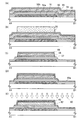
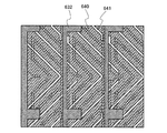
本実施の形態では、半導体装置(表示装置)に用いられる薄膜トランジスタの作製工程について、図1乃至図4を用いて説明する。図1乃至図3は、薄膜トランジスタの作製工程を示す断面図であり、図4は一画素における薄膜トランジスタ及び画素電極の接続領域の平面図であり、図1乃至図3は、図4における線A1−B1の薄膜トランジスタの作製工程を示す断面図である。
(Embodiment 1)
In this embodiment, a manufacturing process of a thin film transistor used for a semiconductor device (display device) will be described with reference to FIGS. 1 to 3 are cross-sectional views illustrating a manufacturing process of a thin film transistor, FIG. 4 is a plan view of a connection region of a thin film transistor and a pixel electrode in one pixel, and FIGS. It is sectional drawing which shows the manufacturing process of the thin-film transistor of B1.
微結晶半導体膜を有する薄膜トランジスタはp型よりもn型の方が、移動度が高いので駆動回路に用いるのにより適しているが、本発明では、薄膜トランジスタはn型であってもp型であってもどちらでも良い。いずれの極性の薄膜トランジスタを用いる場合でも、同一の基板上に形成する薄膜トランジスタを全て同じ極性にそろえておくことが、工程数を抑えるためにも望ましい。ここでは、nチャネル型の薄膜トランジスタを用いて説明する。 A thin film transistor having a microcrystalline semiconductor film is more suitable for use in a driver circuit because the n-type has higher mobility than the p-type, but in the present invention, the thin-film transistor is p-type even if it is n-type. But either is fine. Regardless of which thin film transistor is used, it is desirable to keep all thin film transistors formed on the same substrate to have the same polarity in order to reduce the number of steps. Here, description is made using an n-channel thin film transistor.
以下、作製方法を詳細に説明する。基板50上にゲート電極51を形成する。基板50は、バリウムホウケイ酸ガラス、アルミノホウケイ酸ガラス、若しくはアルミノシリケートガラスなど、フュージョン法やフロート法で作製される無アルカリガラス基板、セラミック基板の他、本作製工程の処理温度に耐えうる耐熱性を有するプラスチック基板等を用いることができる。また、ステンレス合金などの金属基板の表面に絶縁膜を設けた基板を適用しても良い。基板50の大きさは、第1世代と呼ばれる300mm×400mmから、第3世代の550mm×650mm、第4世代の730mm×920mm、第5世代の1000mm×1200mm、第6世代の1500mm×1850mm、第7世代の1870mm×2200mm、第8世代の2200mm×2400mm、第9世代の2400mm×2800mm、第10世代の2880mm×3080mmなど様々なサイズを適用することができる。
Hereinafter, the production method will be described in detail. A
ゲート電極51は、チタン、モリブデン、クロム、タンタル、タングステン、アルミニウムなどの金属材料またはその合金材料を用いて形成する。ゲート電極51は、スパッタリング法や真空蒸着法で基板50上に導電膜を形成し、当該導電膜上にフォトリソグラフィ技術またはインクジェット法によりマスクを形成し、当該マスクを用いて導電膜をエッチングすることで、形成することができる。また、銀、金、銅などの導電性ナノペーストを用いてインクジェット法により吐出し焼成して、ゲート電極51を形成することができる。なお、ゲート電極51の密着性向上と下地への拡散を防ぐバリアメタルとして、上記金属材料の窒化物膜を、基板50及びゲート電極51の間に設けてもよい。また、ゲート電極51は積層構造としてもよく、基板50側からアルミニウム膜とモリブデン膜の積層、銅膜とモリブデン膜との積層、銅膜と窒化チタン膜との積層、銅膜と窒化タンタル膜との積層などを用いることができる。上記積層構造において、上層に形成されるモリブデン膜や、窒化チタン膜、窒化タンタル膜などの窒化物膜はバリアメタルとしての効果を有する。
The
なお、ゲート電極51上には半導体膜や配線を形成するので、段切れ防止のため端部がテーパー状になるように加工することが望ましい。また、図示しないがこの工程でゲート電極51に接続する配線も同時に形成することができる。
Note that since a semiconductor film or a wiring is formed over the
次に、ゲート電極51上に、ゲート絶縁膜52a、52b、微結晶半導体膜53、非晶質半導体膜54、一導電型を付与する不純物が添加された非晶質半導体膜55を順に形成する(図1(A)及び図4(A)参照。)。図1(A)は、図4(A)のA1−B1の断面図に相当する。
Next,
微結晶半導体膜53を、水素プラズマを作用させつつ(作用させた)ゲート絶縁膜52b表面に形成してもよい。水素プラズマを作用させたゲート絶縁膜上に微結晶半導体膜を形成すると、微結晶の結晶成長を促進することができる。
The
また、ゲート絶縁膜及び微結晶半導体膜の界面における格子歪を低減することが可能であり、ゲート絶縁膜及び微結晶半導体膜の界面特性を向上させることができる。従って得られる微結晶半導体膜は電気特性が高く信頼性のよいものとすることができる。 In addition, lattice distortion at the interface between the gate insulating film and the microcrystalline semiconductor film can be reduced, and the interface characteristics between the gate insulating film and the microcrystalline semiconductor film can be improved. Therefore, the obtained microcrystalline semiconductor film can have high electric characteristics and high reliability.
なお、ゲート絶縁膜52a、52b、微結晶半導体膜53、及び非晶質半導体膜54を大気に触れさせることなく連続的に形成してもよい。ゲート絶縁膜52a、52b、微結晶半導体膜53、非晶質半導体膜54を大気に触れさせることなく連続成膜することで、大気成分や大気中に浮遊する汚染不純物元素に汚染されることなく各積層界面を形成することができるので、薄膜トランジスタ特性のばらつきを低減することができる。
Note that the
ゲート絶縁膜52a、52bはそれぞれ、CVD法やスパッタリング法等を用いて、酸化珪素膜、窒化珪素膜、酸化窒化珪素膜、または窒化酸化珪素膜で形成することができる。ここでは、ゲート絶縁膜52a、52bとして、窒化珪素膜または窒化酸化珪素膜と、酸化珪素膜または酸化窒化珪素膜との順に積層して形成する形態を示す。なお、ゲート絶縁膜を2層とせず、基板側から窒化珪素膜または窒化酸化珪素膜と、酸化珪素膜または酸化窒化珪素膜と、窒化珪素膜または窒化酸化珪素膜との順に3層積層して形成することができる。また、ゲート絶縁膜を、酸化珪素膜、窒化珪素膜、酸化窒化珪素膜、または窒化酸化珪素膜の単層で形成することができる。更には、周波数が1GHzのマイクロ波プラズマCVD装置を用いてゲート絶縁膜を形成することが好ましい。マイクロ波プラズマCVD装置で形成した酸化窒化珪素膜、窒化酸化珪素膜は、耐圧が高く、後に形成される薄膜トランジスタの信頼性を高めることができる。
Each of the
ゲート絶縁膜の3層積層構造の例として、ゲート電極上に1層目として窒化珪素膜または窒化酸化珪素膜と、2層目として酸化窒化珪素膜と、3層目として窒化珪素膜とを積層とし、最上層の窒化珪素膜上に微結晶半導体膜を形成してもよい。この場合、1層目の窒化珪素膜または窒化酸化珪素膜は膜厚が50nmより厚い方がよく、ナトリウムなどの不純物を遮断するバリア、ゲート電極のヒロックの防止、ゲート電極の酸化防止などの効果を奏する。3層目の窒化珪素膜は微結晶半導体膜の密着性向上、酸化防止としての効果を奏する。 As an example of a three-layer structure of a gate insulating film, a silicon nitride film or a silicon nitride oxide film as a first layer, a silicon oxynitride film as a second layer, and a silicon nitride film as a third layer are stacked on the gate electrode A microcrystalline semiconductor film may be formed over the uppermost silicon nitride film. In this case, the thickness of the first silicon nitride film or silicon nitride oxide film is preferably larger than 50 nm, and effects such as a barrier that blocks impurities such as sodium, prevention of hillocks in the gate electrode, and prevention of oxidation of the gate electrode Play. The third silicon nitride film has the effect of improving the adhesion of the microcrystalline semiconductor film and preventing oxidation.
このようにゲート絶縁膜表面に極薄膜の窒化珪素膜のような窒化膜を形成することで微結晶半導体膜の密着性を向上することができる。窒化膜はプラズマCVD法により成膜してもよく、マイクロ波による高密度で低温なプラズマ処理によって窒化処理を行ってもよい。また、反応室にシランフラッシュ処理を行う際に窒化珪素膜、窒化酸化珪素膜を形成してもよい。 Thus, by forming a nitride film such as an extremely thin silicon nitride film on the surface of the gate insulating film, the adhesion of the microcrystalline semiconductor film can be improved. The nitride film may be formed by a plasma CVD method, or nitridation may be performed by high-density and low-temperature plasma treatment using microwaves. Further, a silicon nitride film or a silicon nitride oxide film may be formed when the silane flash treatment is performed in the reaction chamber.
ここでは、酸化窒化珪素膜とは、その組成として、窒素よりも酸素の含有量が多いものであって、濃度範囲として酸素が55〜65原子%、窒素が1〜20原子%、Siが25〜35原子%、水素が0.1〜10原子%の範囲で含まれるものをいう。また、窒化酸化珪素膜とは、その組成として、酸素よりも窒素の含有量が多いものであって、濃度範囲として酸素が15〜30原子%、窒素が20〜35原子%、Siが25〜35原子%、水素が15〜25原子%の範囲で含まれるものをいう。 Here, the silicon oxynitride film has a composition that contains more oxygen than nitrogen and has a concentration range of 55 to 65 atomic%, 1 to 20 atomic%, and 25 Si. -35 atomic%, and hydrogen is contained in the range of 0.1-10 atomic%. The silicon nitride oxide film has a composition containing more nitrogen than oxygen, and the concentration ranges of oxygen are 15 to 30 atomic%, nitrogen is 20 to 35 atomic%, and Si is 25 to 25%. 35 atomic% and hydrogen are included in the range of 15 to 25 atomic%.
一導電型を付与する不純物が添加された非晶質半導体膜55は、nチャネル型の薄膜トランジスタを形成する場合には、代表的な不純物元素としてリンを添加すれば良く、水素化珪素にPH3などの不純物気体を加えれば良い。また、pチャネル型の薄膜トランジスタを形成する場合には、代表的な不純物元素としてボロンを添加すれば良く、水素化珪素にB2H6などの不純物気体を加えれば良い。一導電型を付与する不純物が添加された非晶質半導体膜55は、微結晶半導体膜、または非晶質半導体膜で形成することができる。一導電型を付与する不純物が添加された非晶質半導体膜55は膜厚2〜50nm(好ましくは10〜30nm)とすればよい。
微結晶半導体膜53、非晶質半導体膜54、及び一導電型を付与する不純物が添加された非晶質半導体膜55上にマスク56を形成する(図1(B)参照。)。マスク56は、フォトリソグラフィ技術またはインクジェット法により形成する。
A
次に、マスク56を用いて微結晶半導体膜53、非晶質半導体膜54、及び一導電型を付与する不純物が添加された非晶質半導体膜55をエッチングし分離して、微結晶半導体膜57、非晶質半導体膜58、及び一導電型を付与する不純物が添加された非晶質半導体膜69を形成する(図1(C)参照。)。この後、マスク56を除去する。なお、図1(C)は、図4(B)のA1−B1の断面図に相当する。
Next, the
微結晶半導体膜57、非晶質半導体膜58、及び一導電型を付与する不純物が添加された非晶質半導体膜69の端部をテーパーを有する形状にエッチングしてもよい。端部のテーパー角は90°〜30°、好ましくは80°〜45°とする。これにより、段差形状による配線の段切れを防ぐことができる。
The ends of the
次に、微結晶半導体膜57、非晶質半導体膜58、一導電型を付与する不純物が添加された非晶質半導体膜69及びゲート絶縁膜52b上に導電膜65aを形成する(図1(D)参照。)。
Next, a
導電膜65aにレーザ光60を照射し、一導電型を付与する不純物が添加された非晶質半導体膜69及び非晶質半導体膜58を結晶化(微結晶化)し、一導電型を付与する不純物が添加された微結晶半導体膜63、及び微結晶半導体層62を形成する(図1(E)参照。)。
The
レーザ光60により微結晶半導体膜57上の非晶質半導体膜58は結晶化し、成膜法による微結晶半導体膜57を含む微結晶半導体層62を形成することができる。成膜法による微結晶半導体膜57は、非晶質半導体膜58の結晶成長の核となりうる。
The
導電膜65aはレーザ光60の照射工程において、下層の半導体膜の酸化、汚染等を防ぐ保護膜としても機能する。従って、工程時における半導体膜の酸化等の劣化を防止できるため、信頼性が向上する。従って信頼性の高い薄膜トランジスタを有する表示装置を作製することができる。
The
また、一導電型を付与する不純物が添加された微結晶半導体膜をソース領域及びドレイン領域として用いるため、ソース領域及びドレイン領域を低抵抗化でき、薄膜トランジスタの電気特性を向上させることができる。 In addition, since the microcrystalline semiconductor film to which an impurity imparting one conductivity type is added is used for the source region and the drain region, the resistance of the source region and the drain region can be reduced and the electrical characteristics of the thin film transistor can be improved.
さらに本発明では、レーザ光を照射された導電膜をエッチングし、ソース電極及びドレイン電極を形成する。従って、微結晶半導体層を形成するレーザ照射工程のための導電膜の形成、除去を行わないので、工程が簡略化できる。従って歩留まりも向上し量産性高く薄膜トランジスタ、及び該薄膜トランジスタを有する表示装置を作製することができる。 Further, in the present invention, the conductive film irradiated with the laser light is etched to form a source electrode and a drain electrode. Accordingly, since the conductive film is not formed or removed for the laser irradiation process for forming the microcrystalline semiconductor layer, the process can be simplified. Accordingly, the yield can be improved and a thin film transistor and a display device including the thin film transistor can be manufactured with high productivity.
レーザ光を照射する導電膜65aは、タングステン(W)、クロム(Cr)、タンタル(Ta)、窒化タンタルまたはモリブデン(Mo)などの高融点金属、又は高融点金属を主成分とする合金もしくは化合物(例えば、これらの金属元素の窒化物)を用いることが好ましい。
The
導電膜に照射する光は導電膜に高いエネルギーを与えられるものであればよく、好適にはレーザ光を用いることができる。 The light applied to the conductive film may be any light as long as it can apply high energy to the conductive film, and laser light can be preferably used.
光の波長は、導電膜に吸収される波長とする。その波長は、光の表皮深さ(skin depth)などを考慮して決定することができる。また、光のエネルギーは、光の波長、光の表皮深さ、照射する導電膜の膜厚などを考慮して決定することができる。導電膜に光が吸収されるように、導電膜の材料や光の波長や照射条件は適宜設定すればよい。 The wavelength of light is a wavelength absorbed by the conductive film. The wavelength can be determined in consideration of the skin depth of light. The energy of light can be determined in consideration of the wavelength of light, the skin depth of light, the thickness of the conductive film to be irradiated, and the like. What is necessary is just to set the material of a conductive film, the wavelength of light, and irradiation conditions suitably so that light may be absorbed in a conductive film.
レーザ光を発振するレーザは、連続発振レーザ、疑似連続発振レーザ及びパルス発振レーザを用いることができる。例えば、KrFレーザなどのエキシマレーザ、Arレーザ、Krレーザなどの気体レーザがある。その他、固体レーザとして、YAGレーザ、YVO4レーザ、YLFレーザ、YAlO3レーザ、GdVO4レーザ、KGWレーザ、KYWレーザ、アレキサンドライトレーザ、Ti:サファイアレーザ、Y2O3レーザなどがある。なお、エキシマレーザはパルス発振レーザであるが、YAGレーザなどの固体レーザには、連続発振レーザにも、疑似連続発振レーザにも、パルス発振レーザにもなるものがある。なお、固体レーザにおいては、基本波の第2高調波〜第5高調波を適用するのが好ましい。また、GaN、GaAs、GaAlAs、InGaAsP等の半導体レーザも用いることができる。 As a laser that oscillates laser light, a continuous wave laser, a pseudo continuous wave laser, or a pulsed laser can be used. For example, there is an excimer laser such as a KrF laser, or a gas laser such as an Ar laser or a Kr laser. Other solid-state lasers include YAG laser, YVO 4 laser, YLF laser, YAlO 3 laser, GdVO 4 laser, KGW laser, KYW laser, alexandrite laser, Ti: sapphire laser, and Y 2 O 3 laser. An excimer laser is a pulsed laser, but some solid-state lasers such as a YAG laser can be a continuous wave laser, a pseudo continuous wave laser, or a pulsed laser. In the solid-state laser, it is preferable to apply the second to fifth harmonics of the fundamental wave. A semiconductor laser such as GaN, GaAs, GaAlAs, InGaAsP, or the like can also be used.
また、ランプ光を用いてもよい。例えば、紫外線ランプ、ブラックライト、ハロゲンランプ、メタルハライドランプ、キセノンアークランプ、カーボンアークランプ、高圧ナトリウムランプ、または高圧水銀ランプから射出された光を用いてもよい。上記ランプ光を用いたフラッシュアニールを用いてもよい。ハロゲンランプやキセノンランプなどを好適に用いて行うフラッシュアニールは極短時間の処理でよいため、支持基板の温度上昇を抑えることができる。 Further, lamp light may be used. For example, light emitted from an ultraviolet lamp, black light, halogen lamp, metal halide lamp, xenon arc lamp, carbon arc lamp, high pressure sodium lamp, or high pressure mercury lamp may be used. Flash annealing using the lamp light may be used. The flash annealing performed suitably using a halogen lamp, a xenon lamp, or the like may be performed in a very short time, and thus the temperature rise of the support substrate can be suppressed.
光の形状や光の進路を調整するため、シャッター、ミラー又はハーフミラー等の反射体、シリンドリカルレンズや凸レンズなどによって構成される光学系が設置されていてもよい。 In order to adjust the shape of light and the path of light, an optical system including a reflector such as a shutter, a mirror, or a half mirror, a cylindrical lens, or a convex lens may be installed.
なお、光の照射方法は、選択的に光を照射してもよいし、光をXY軸方向に走査して光を照射することができる。この場合、光学系にポリゴンミラーやガルバノミラーを用いることが好ましい。 Note that the light irradiation method may selectively irradiate light, or light may be irradiated by scanning light in the XY axis direction. In this case, it is preferable to use a polygon mirror or a galvanometer mirror for the optical system.
微結晶半導体層62は、ギブスの自由エネルギーを考慮すれば非晶質と単結晶の中間的な準安定状態に属するものである。すなわち、自由エネルギー的に安定な第3の状態を有する半導体であって、短距離秩序を持ち格子歪みを有する。柱状または針状結晶が基板表面に対して法線方向に成長している。微結晶半導体の代表例である微結晶シリコンは、そのラマンスペクトルが単結晶シリコンを示す520cm−1よりも低周波数側に、シフトしている。即ち、単結晶シリコンを示す520cm−1とアモルファスシリコンを示す480cm−1の間に微結晶シリコンのラマンスペクトルのピークがある。また、未結合手(ダングリングボンド)を終端するため水素またはハロゲンを少なくとも1原子%またはそれ以上含ませている。さらに、ヘリウム、アルゴン、クリプトン、ネオンなどの希ガス元素を含ませて格子歪みをさらに助長させることで、安定性が増し良好な微結晶半導体膜が得られる。
In consideration of Gibbs free energy, the
この微結晶半導体層は、周波数が数十MHz〜数百MHzの高周波プラズマCVD法、または周波数が1GHz以上のマイクロ波プラズマCVD装置により形成することができる。代表的には、SiH4、Si2H6、SiH2Cl2、SiHCl3、SiCl4、SiF4などの水素化珪素を水素で希釈して形成することができる。また、水素化珪素及び水素に加え、ヘリウム、アルゴン、クリプトン、ネオンから選ばれた一種または複数種の希ガス元素で希釈して微結晶半導体膜を形成することができる。これらのときの水素化珪素に対して水素の流量比を5倍以上200倍以下、好ましくは50倍以上150倍以下、更に好ましくは100倍とする。 This microcrystalline semiconductor layer can be formed by a high-frequency plasma CVD method with a frequency of several tens to several hundreds of MHz or a microwave plasma CVD apparatus with a frequency of 1 GHz or more. Typically, silicon hydride such as SiH 4 , Si 2 H 6 , SiH 2 Cl 2 , SiHCl 3 , SiCl 4 , and SiF 4 can be formed by diluting with hydrogen. In addition to silicon hydride and hydrogen, the microcrystalline semiconductor film can be formed by dilution with one or more kinds of rare gas elements selected from helium, argon, krypton, and neon. The flow rate ratio of hydrogen to silicon hydride at these times is 5 to 200 times, preferably 50 to 150 times, and more preferably 100 times.
また、微結晶半導体層は、価電子制御を目的とした不純物元素を意図的に添加しないときに弱いn型の電気伝導性を示すので、薄膜トランジスタのチャネル形成領域として機能する微結晶半導体層に対しては、p型を付与する不純物元素を、成膜と同時に、或いは成膜後に添加することで、しきい値制御をすることが可能となる。p型を付与する不純物元素としては、代表的には硼素であり、B2H6、BF3などの不純物気体を1ppm〜1000ppm、好ましくは1〜100ppmの割合で水素化珪素に混入させると良い。そしてボロンの濃度を、例えば1×10¹⁴〜6×10¹⁶atoms/cm3とすると良い。 In addition, since the microcrystalline semiconductor layer exhibits weak n-type conductivity when an impurity element for the purpose of valence electron control is not intentionally added, the microcrystalline semiconductor layer has a lower resistance than a microcrystalline semiconductor layer that functions as a channel formation region of a thin film transistor. Thus, the threshold value can be controlled by adding an impurity element imparting p-type at the same time as film formation or after film formation. The impurity element imparting p-type is typically boron, and an impurity gas such as B 2 H 6 or BF 3 may be mixed into silicon hydride at a rate of 1 ppm to 1000 ppm, preferably 1 to 100 ppm. . The boron concentration is preferably 1 × 10 14 to 6 × 10 16 atoms / cm 3 , for example.
また、微結晶半導体層の酸素濃度を、5×10¹⁹atoms/cm3以下、好ましくは1×1019atoms/cm3以下、窒素及び炭素の濃度それぞれを1×1018atoms/cm3以下とすることが好ましい。酸素、窒素、及び炭素が微結晶半導体膜に混入する濃度を低減することで、微結晶半導体膜がn型化になることを防止することができる。 The oxygen concentration of the microcrystalline semiconductor layer is 5 × 10 19 atoms / cm 3 or less, preferably 1 × 10 19 atoms / cm 3 or less, and the nitrogen and carbon concentrations are 1 × 10 18 atoms / cm 3 or less, respectively. It is preferable to do. By reducing the concentration of oxygen, nitrogen, and carbon in the microcrystalline semiconductor film, the microcrystalline semiconductor film can be prevented from becoming n-type.
本発明において、微結晶半導体層62は、成膜法による微結晶半導体膜53及び非晶質半導体膜54がレーザ光照射工程によって微結晶化した微結晶半導体膜により形成されている。よって微結晶半導体層62の膜厚は結晶成長の核となる成膜法による微結晶半導体膜53と非晶質半導体膜54のほぼ合計となる。微結晶半導体層62の膜厚は、25〜300nm(好ましくは30〜150nm)程度とすればよい。また、成膜法による微結晶半導体膜53は非晶質半導体膜54の結晶成長の核として機能すればよいので、膜厚は薄くても良く、極薄膜でも構わない。非晶質半導体膜54は、微結晶半導体膜53上に積層した状態で結晶化されるため、高い電気特性及び信頼性を有する微結晶状態の微結晶半導体層とすることができる。
In the present invention, the
また、微結晶半導体層62を、0nmより厚く50nm以下、好ましくは0nmより厚く20nm以下で形成してもよい。微結晶半導体層62は後に形成される薄膜トランジスタのチャネル形成領域として機能する。微結晶半導体層62の厚さを上記の範囲内とすることで、後に形成される薄膜トランジスタは、完全空乏型とすることができる。
The
また、微結晶半導体層は微結晶で構成されているため、非晶質半導体膜と比較して抵抗が低い。このため、微結晶半導体膜を用いた薄膜トランジスタは、電流電圧特性を示す曲線の立ち上がり部分の傾きが急峻となり、スイッチング素子としての応答性が優れ、高速動作が可能となる。また、薄膜トランジスタのチャネル形成領域に微結晶半導体層を用いることで、薄膜トランジスタの閾値の変動を抑制することが可能である。このため、電気特性のばらつきの少ない表示装置を作製することができる。 In addition, since the microcrystalline semiconductor layer includes microcrystals, the resistance is lower than that of the amorphous semiconductor film. Therefore, a thin film transistor using a microcrystalline semiconductor film has a steep slope at a rising portion of a curve indicating current-voltage characteristics, has excellent response as a switching element, and can operate at high speed. In addition, when a microcrystalline semiconductor layer is used for a channel formation region of the thin film transistor, variation in the threshold value of the thin film transistor can be suppressed. Therefore, a display device with little variation in electrical characteristics can be manufactured.
また、微結晶半導体膜は非晶質半導体膜と比較して移動度が高い。このため、表示素子のスイッチングとして、チャネル形成領域が微結晶半導体膜で形成される薄膜トランジスタを用いることで、チャネル形成領域の面積、即ち薄膜トランジスタの面積を縮小することが可能である。このため、一画素あたりに示す薄膜トランジスタの面積が小さくなり、画素の開口率を高めることが可能である。この結果、解像度の高い装置を作製することができる。 In addition, the microcrystalline semiconductor film has higher mobility than the amorphous semiconductor film. Therefore, the area of the channel formation region, that is, the area of the thin film transistor can be reduced by using a thin film transistor in which the channel formation region is formed using a microcrystalline semiconductor film for switching the display element. Therefore, the area of the thin film transistor shown per pixel is reduced, and the aperture ratio of the pixel can be increased. As a result, a device with high resolution can be manufactured.
また、微結晶半導体膜は下側から縦方向に成長し、針状結晶である。微結晶半導体膜には非晶質と結晶構造が混在しており、結晶領域と非晶質領域との間に局部応力でクラックが発生し、隙間ができやすい。この隙間に新たなラジカルが介入して結晶成長を起こしうる。しかし上方の結晶面が大きくなるため、針状に上方に成長しやすい。このように微結晶半導体膜は縦方向に成長しても、非晶質半導体膜の成膜速度に比べて1/10〜1/100の早さである。 The microcrystalline semiconductor film grows in the vertical direction from the lower side and is a needle-like crystal. A microcrystalline semiconductor film has both an amorphous structure and a crystalline structure, and a crack is generated by a local stress between the crystalline region and the amorphous region, so that a gap is easily formed. New radicals can intervene in this gap to cause crystal growth. However, since the upper crystal plane becomes large, it tends to grow upward in a needle shape. Thus, even if the microcrystalline semiconductor film is grown in the vertical direction, it is 1/10 to 1/100 faster than the deposition rate of the amorphous semiconductor film.
本発明では、成膜法による微結晶半導体膜上に非晶質半導体膜を結晶化した微結晶半導体膜を形成し、微結晶半導体層を形成するため、膜厚の厚い微結晶半導体層でも長い工程時間を要しないで形成することができる。よって、微結晶半導体層を有する薄膜トランジスタの形成工程にかかる時間を短縮することができ、生産性が向上する。 In the present invention, a microcrystalline semiconductor film obtained by crystallizing an amorphous semiconductor film is formed over a microcrystalline semiconductor film by a deposition method, and a microcrystalline semiconductor layer is formed. Therefore, even a thick microcrystalline semiconductor layer is long. It can be formed without requiring process time. Thus, the time required for forming a thin film transistor having a microcrystalline semiconductor layer can be shortened, and productivity is improved.
導電膜65aに対するレーザ光照射工程を行った後、導電膜65aと同様にソース電極及びドレイン電極となり配線としても機能する導電膜65b及び導電膜65cを積層する(図2(A)参照。)。
After performing the laser light irradiation process on the
導電膜は、アルミニウム、若しくは銅、シリコン、チタン、ネオジム、スカンジウム、モリブデンなどの耐熱性向上元素若しくはヒロック防止元素が添加されたアルミニウム合金の単層または積層で形成することが好ましい。また、一導電型を付与する不純物が添加された半導体膜と接する側の導電膜65aを、チタン、タンタル、モリブデン、タングステン、またはこれらの元素の窒化物で形成し、その上にアルミニウムまたはアルミニウム合金を形成した積層構造としても良い。更には、アルミニウムまたはアルミニウム合金の上面及び下面を、チタン、タンタル、モリブデン、タングステン、またはこれらの元素の窒化物で挟んだ積層構造としてもよい。ここでは、導電膜としては、導電膜65a〜65c3層が積層した構造の導電膜を示し、導電膜65a、65cにモリブデン膜、導電膜65bにアルミニウム膜を用いた積層導電膜や、導電膜65a、65cにチタン膜、導電膜65bにアルミニウム膜を用いた積層導電膜を示す。本実施の形態のように、レーザ光を照射される導電膜65aに溶融しにくいモリブデンのような高融点材料を用い、一方レーザ光を照射されない導電膜65bには、低融点材料であっても抵抗が低く導電性の高いアルミニウムのような導電性材料を用いることで、高信頼性化、高性能化を両方付与することができる。
The conductive film is preferably formed using a single layer or a stack of aluminum or an aluminum alloy to which a heat resistance improving element such as copper, silicon, titanium, neodymium, scandium, or molybdenum or a hillock prevention element is added. The
導電膜65a〜65cは、スパッタリング法や真空蒸着法で形成する。また、CVD法を用いてもよい。さらに、導電膜65a〜65cは、銀、金、銅などの導電性ナノペーストを用いてスクリーン印刷法、インクジェット法等を用いて吐出し焼成して形成しても良い。
The
次に導電膜65a〜65c上にマスク66を形成する。マスク66は、マスク56と同様に形成することができる。
Next, a
マスク66を用いて導電膜65a〜65cをエッチングし分離して、ソース電極及びドレイン電極71a〜71cを形成する(図2(B)参照。)。本実施の形態のように導電膜65a〜65cをウエットエッチングすると、導電膜65a〜65cは等方的にエッチングされるため、マスク66の端部と、ソース電極及びドレイン電極71a〜71cの端部はより一致せずより後退している。次に、マスク66を用いて一導電型を付与する不純物が添加された微結晶半導体膜63及び微結晶半導体層62をエッチングして、ソース領域及びドレイン領域72、微結晶半導体層73を形成する(図2(C)参照。)。なお、微結晶半導体層73は一部のみがエッチングされ、溝部(凹部)を有する微結晶半導体層である。
The
微結晶半導体層73は一部エッチングされ、ソース電極及びドレイン電極71a〜71c間に溝部が形成されている。この微結晶半導体層73の溝部の端部は、ソース領域及びドレイン領域72の端部とほぼ一致している。この溝部はソース領域及びドレイン領域72を形成するエッチングと同一エッチングプロセスで形成される。従って同一フォトレジストマスクであるマスク66の開口部と概略一致している、セルフアラインプロセスである。
Part of the
ソース電極及びドレイン電極71a〜71cの端部と、ソース領域及びドレイン領域72の端部は一致せずずれており、ソース電極及びドレイン電極71a〜71cの端部の外側に、ソース領域及びドレイン領域72の端部が形成される。この後、マスク66を除去する。なお、図2(C)は、図4(C)のA1−B1の断面図に相当する。図4(C)に示すように、ソース領域及びドレイン領域72の端部は、ソース電極及びドレイン電極71cの端部の外側に位置することが分かる。また、ソース電極またはドレイン電極の一方は、ソース配線またはドレイン配線としても機能する。
The end portions of the source and
図2(C)に示すように、ソース電極及びドレイン電極71a〜71cの端部と、ソース領域及びドレイン領域72の端部は一致せずずれた形状となることで、ソース電極及びドレイン電極71a〜71cの端部の距離が離れるため、ソース電極及びドレイン電極間のリーク電流やショートを防止することができる。このため、信頼性が高く、且つ耐圧の高い薄膜トランジスタを作製することができる。
As shown in FIG. 2C, the end portions of the source and
以上の工程により、チャネルエッチ型の薄膜トランジスタ74を形成することができる。
Through the above process, a channel-etched
次に、ソース電極及びドレイン電極71a〜71c、ソース領域及びドレイン領域72、微結晶半導体膜61、及びゲート絶縁膜52b上に絶縁膜76を形成する(図2(D)参照。)。絶縁膜76は、ゲート絶縁膜52a、52bと同様に形成することができる。なお、絶縁膜76は、大気中に浮遊する有機物や金属物、水蒸気などの汚染不純物の侵入を防ぐためのものであり、緻密な膜が好ましい。
Next, an insulating
次に、絶縁膜76にコンタクトホールを形成し、当該コンタクトホールにおいてソース電極及びドレイン電極71cに接する画素電極77を形成する。なお、図3(A)は、図4(D)のA1−B1の断面図に相当する。
Next, a contact hole is formed in the insulating
画素電極77は、酸化タングステンを含むインジウム酸化物、酸化タングステンを含むインジウム亜鉛酸化物、酸化チタンを含むインジウム酸化物、酸化チタンを含むインジウム錫酸化物、インジウム錫酸化物(以下、ITOと示す。)、インジウム亜鉛酸化物、酸化ケイ素を添加したインジウム錫酸化物などの透光性を有する導電性材料を用いることができる。
The
また、画素電極77として、導電性高分子(導電性ポリマーともいう)を含む導電性組成物を用いて形成することができる。導電性組成物を用いて形成した画素電極は、シート抵抗が10000Ω/□以下、波長550nmにおける透光率が70%以上であることが好ましい。また、導電性組成物に含まれる導電性高分子の抵抗率が0.1Ω・cm以下であることが好ましい。
The
導電性高分子としては、いわゆるπ電子共役系導電性高分子が用いることができる。例えば、ポリアニリンまたはその誘導体、ポリピロールまたはその誘導体、ポリチオフェンまたはその誘導体、若しくはこれらの2種以上の共重合体などがあげられる。 As the conductive polymer, a so-called π-electron conjugated conductive polymer can be used. For example, polyaniline or a derivative thereof, polypyrrole or a derivative thereof, polythiophene or a derivative thereof, or a copolymer of two or more kinds thereof can be given.
また、ソース領域及びドレイン領域72の端部とソース電極及びドレイン電極71a〜71cの端部を一致する形状としてもよい。図3(B)にソース領域及びドレイン領域72の端部とソース電極及びドレイン電極71a〜71cの端部が一致する形状のチャネルエッチ型の薄膜トランジスタ79を示す。ソース電極及びドレイン電極71a〜71cのエッチング及びソース領域及びドレイン領域72のエッチングをドライエッチングで行うと薄膜トランジスタ79のような形状にすることができる。また、一導電型を付与する不純物が添加された半導体膜をソース電極及びドレイン電極71a〜71cをマスクとしてエッチングし、ソース領域及びドレイン領域72を形成しても薄膜トランジスタ79のような形状にすることができる。
Alternatively, the end portions of the source and drain
チャネルエッチ型の薄膜トランジスタは、作製工程数が少なく、コスト削減が可能である。また、微結晶半導体膜でチャネル形成領域を構成することにより1〜20cm2/V・secの電界効果移動度を得ることができる。従って、この薄膜トランジスタを画素部の画素のスイッチング用素子として、さらに走査線(ゲート線)側の駆動回路を形成する素子として利用することができる。 A channel-etched thin film transistor has a small number of manufacturing steps and can reduce costs. Further, field effect mobility of 1 to 20 cm 2 / V · sec can be obtained by forming a channel formation region using a microcrystalline semiconductor film. Therefore, this thin film transistor can be used as an element for switching a pixel in the pixel portion and an element for forming a driving circuit on the scanning line (gate line) side.
本実施の形態により、電気特性が高く信頼性のよい薄膜トランジスタを有する表示装置を量産性高く作製することができる。 According to this embodiment mode, a display device including a thin film transistor with high electrical characteristics and high reliability can be manufactured with high productivity.
(実施の形態2)
本実施の形態は、実施の形態1において、薄膜トランジスタの形状が異なる例である。従って、他は実施の形態1と同様に行うことができ、実施の形態1と同一部分又は同様な機能を有する部分、及び工程の繰り返しの説明は省略する。
(Embodiment 2)
This embodiment is an example in which the shape of a thin film transistor is different from that in
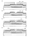
本実施の形態では、表示装置に用いられる薄膜トランジスタ及びその作製工程について、図5乃至図8を用いて説明する。図5乃至図7は、薄膜トランジスタ及び画素電極の作製方法を示す断面図であり、図8は一画素における薄膜トランジスタ及び画素電極の接続領域の平面図である。図5乃至図7は、図8における線A2−B2の薄膜トランジスタ及びその作製工程を示す断面図に相当する。 In this embodiment, a thin film transistor used for a display device and a manufacturing process thereof will be described with reference to FIGS. 5 to 7 are cross-sectional views illustrating a method for manufacturing a thin film transistor and a pixel electrode, and FIG. 8 is a plan view of a connection region of the thin film transistor and the pixel electrode in one pixel. 5 to 7 correspond to cross-sectional views illustrating the thin film transistor taken along line A2-B2 in FIG. 8 and a manufacturing process thereof.
基板250上にゲート電極251を形成する。次に、ゲート電極251上に、ゲート絶縁膜252a、252b、微結晶半導体膜253、非晶質半導体膜254、一導電型を付与する不純物が添加された非晶質半導体膜255、導電膜265aを順に形成する(図5(A)及び図8(A)参照。)。図5(A)は、図8(A)のA2−B2の断面図に相当する。
A
本実施の形態では、レーザ光照射工程の後、微結晶半導体層、一導電型を付与する不純物が添加された微結晶半導体膜のエッチング工程をソース電極及びドレイン電極と同工程で行う例を示す。従って、微結晶半導体層、一導電型を付与する不純物が添加された微結晶半導体膜、ソース電極及びドレイン電極は同じマスク形状を反映して形成される。 In this embodiment, after the laser light irradiation process, an etching process of the microcrystalline semiconductor layer and the microcrystalline semiconductor film to which an impurity imparting one conductivity type is added is performed in the same process as the source electrode and the drain electrode. . Accordingly, the microcrystalline semiconductor layer, the microcrystalline semiconductor film to which an impurity imparting one conductivity type is added, the source electrode, and the drain electrode are formed to reflect the same mask shape.
ゲート絶縁膜252a、252b、微結晶半導体膜253、及び非晶質半導体膜254、一導電型を付与する不純物が添加された非晶質半導体膜255を大気に触れさせることなく連続的に形成してもよい。さらに導電膜265aまで大気に触れさせることなく連続的に形成してもよい。ゲート絶縁膜252a、252b、微結晶半導体膜253、非晶質半導体膜254、一導電型を付与する不純物が添加された非晶質半導体膜255(及び導電膜265a)を大気に触れさせることなく連続成膜することで、大気成分や大気中に浮遊する汚染不純物元素に汚染されることなく各積層界面を形成することができるので、薄膜トランジスタ特性のばらつきを低減することができる。
The
導電膜265aにレーザ光260を照射し、一導電型を付与する不純物が添加された非晶質半導体膜255及び非晶質半導体膜254を結晶化(微結晶化)し、一導電型を付与する不純物が添加された微結晶半導体膜283、及び微結晶半導体層282を形成する(図5(B)参照。)。
The
レーザ光260により微結晶半導体膜253上の非晶質半導体膜254は結晶化し、成膜法による微結晶半導体膜253を含む微結晶半導体層282を形成することができる。成膜法による微結晶半導体膜253は、非晶質半導体膜254の結晶成長の核となりうる。
The
導電膜265aはレーザ光260の照射工程において、下層の半導体膜の酸化、汚染等を防ぐ保護膜としても機能する。従って、工程時における半導体膜の酸化等の劣化を防止できるため、信頼性が向上する。従って信頼性の高い薄膜トランジスタを有する表示装置を作製することができる。
The
さらに本発明では、レーザ光260を照射された導電膜265aをエッチングし、ソース電極及びドレイン電極を形成する。従って、微結晶半導体層を形成するレーザ光照射工程のための導電膜の形成、除去を行わないので、工程が簡略化できる。従って歩留まりも向上し量産性高く薄膜トランジスタ、及び該薄膜トランジスタを有する表示装置を作製することができる。
Further, in the present invention, the
本実施の形態では、マスク256を形成するために高階調マスクを用いた露光を行う例を示す。マスク256を形成するためレジストを形成する。レジストは、ポジ型レジストまたはネガ型レジストを用いることができる。ここでは、ポジ型レジストを用いて示す。
In this embodiment, an example in which exposure using a high-tone mask is performed in order to form the
次に、フォトマスクとして多階調マスク59を用いて、レジストに光を照射して、レジストを露光する。
Next, using the
ここで、多階調マスク59を用いた露光について、図11を用いて説明する。
Here, exposure using the
多階調マスクとは、露光部分、中間露光部分、及び未露光部分に3つの露光レベルを行うことが可能なマスクであり、一度の露光及び現像工程により、複数(代表的には二種類)の厚さの領域を有するレジストマスクを形成することが可能である。このため、多階調マスクを用いることで、フォトマスクの枚数を削減することが可能である。 A multi-tone mask is a mask capable of performing three exposure levels on an exposed portion, an intermediate exposed portion, and an unexposed portion, and a plurality of (typically two types) can be obtained by one exposure and development process. It is possible to form a resist mask having a region with a thickness of. Therefore, the number of photomasks can be reduced by using a multi-tone mask.
多階調マスクの代表例としては、図11(A)に示すようなグレートーンマスク59a、図11(C)に示すようなハーフトーンマスク59bがある。
Typical examples of the multi-tone mask include a gray-
図11(A)に示すように、グレートーンマスク59aは、透光性を有する基板163及びその上に形成される遮光部164並びに回折格子165で構成される。遮光部164においては、光の透過量(透光量)が0%である。一方、回折格子165はスリット、ドット、メッシュ等の光透過部の間隔を、露光に用いる光の解像度限界以下の間隔とすることにより、光の透過量を制御することができる。なお、回折格子165は、周期的なスリット、ドット、メッシュ、または非周期的なスリット、ドット、メッシュどちらも用いることができる。
As shown in FIG. 11A, the
透光性を有する基板163は、石英等の透光性を有する基板を用いることができる。遮光部164及び回折格子165は、クロムや酸化クロム等の光を吸収する遮光材料を用いて形成することができる。
As the
グレートーンマスク59aに露光光を照射した場合、図11(B)に示すように、遮光部164においては、光透過量166は0%であり、遮光部164及び回折格子165が設けられていない領域では光透過量166は100%である。また、回折格子165においては、10〜70%の範囲で調整可能である。回折格子165における光の透過量の調整は、回折格子のスリット、ドット、またはメッシュの間隔及びピッチの調整により可能である。
When the gray-
図11(C)に示すように、ハーフトーンマスク59bは、透光性を有する基板163及びその上に形成される半透過部167並びに遮光部168で構成される。半透過部167は、MoSiN、MoSi、MoSiO、MoSiON、CrSiなどを用いることができる。遮光部168は、クロムや酸化クロム等の光を吸収する遮光材料を用いて形成することができる。
As shown in FIG. 11C, the
ハーフトーンマスク59bに露光光を照射した場合、図11(D)に示すように、遮光部168においては、光透過量169は0%であり、遮光部168及び半透過部167が設けられていない領域では光透過量169は100%である。また、半透過部167においては、10〜70%の範囲で調整可能である。半透過部167に於ける光の透過量の調整は、半透過部167の材料により調整により可能である。
When the
多階調マスク59を用いて露光した後、現像することで、図5(C)に示すように、膜厚の異なる領域を有するマスク256を形成することができる。
By developing after exposure using the
次に、マスク256により、微結晶半導体層282、一導電型を付与する不純物が添加された微結晶半導体膜283、及び導電膜265aをエッチングし分離する。この結果、微結晶半導体層262、一導電型を付与する不純物が添加された微結晶半導体膜263、及び導電膜264を形成することができる(図5(D)参照。)。
Next, with the
次に、マスク256をアッシングする。この結果、マスクの面積が縮小し、厚さが薄くなる。このとき、膜厚の薄い領域のマスクのレジスト(ゲート電極251の一部と重畳する領域)は除去され、分離されたマスク266を形成することができる(図6(A)参照。)。
Next, the
マスク266を用いて導電膜264をエッチングし、ソース電極及びドレイン電極271aを形成する。本実施の形態のように導電膜264をウエットエッチングすると、導電膜264は等方的にエッチングされるため、マスク266の端部と、ソース電極及びドレイン電極271aの端部は一致せずより後退し、ソース電極及びドレイン電極271aの外側に一導電型を付与する不純物が添加された微結晶半導体膜263及び微結晶半導体層262が突出した形状となる。次に、マスク266を用いて一導電型を付与する不純物が添加された微結晶半導体膜263及び微結晶半導体層262をエッチングして、ソース領域及びドレイン領域272、微結晶半導体層273を形成する(図6(B)参照。)。なお、微結晶半導体層273は一部のみがエッチングされ、溝部を有する微結晶半導体層である。
The
ソース領域及びドレイン領域272の形成工程と、微結晶半導体層273の溝部とを同一工程で形成することができ、同様に、微結晶半導体層273の端部が、一部エッチングされ露出した形状となる。この後、マスク266を除去する。
The formation step of the source and drain
次に、ソース電極及びドレイン電極271a、ソース領域及びドレイン領域272、微結晶半導体層273、及びゲート絶縁膜252b上に絶縁膜276を形成する(図6(C)参照。)。
Next, an insulating
次に、絶縁膜276にコンタクトホール284a、284bを形成する(図6(D)及び図8(B)参照。)。なお、図6(D)は、図8(B)のA2−B2の断面図に相当する。
Next,
コンタクトホール284aにソース電極及びドレイン電極271aに接する配線271b、271cを形成する(図7(A)及び図8(C)参照。)。なお、図7(A)は、図8(C)のA2−B2の断面図に相当する。配線271b、271cはソース配線として機能する。以上の工程により、チャネルエッチ型の薄膜トランジスタ274を形成することができる。
コンタクトホール284bにおいてソース電極及びドレイン電極271aに接する画素電極277を形成する(図7(B)及び図8(D)参照。)。なお、図7(B)は、図8(D)のA2−B2の断面図に相当する。
A
また、ソース領域及びドレイン領域272の端部とソース電極及びドレイン電極271aの端部を一致する形状としてもよい。図7(C)にソース領域及びドレイン領域272の端部とソース電極及びドレイン電極271aの端部が一致する形状のチャネルエッチ型の薄膜トランジスタ279を示す。ソース電極及びドレイン電極271aのエッチング及びソース領域及びドレイン領域272のエッチングをドライエッチングで行うと薄膜トランジスタ279のような形状にすることができる。また、一導電型を付与する不純物が添加された半導体膜をソース電極及びドレイン電極271aをマスクとしてエッチングし、ソース領域及びドレイン領域272を形成しても薄膜トランジスタ279のような形状にすることができる。
Alternatively, the end portions of the source and drain
チャネルエッチ型の薄膜トランジスタは、作製工程数が少なく、コスト削減が可能である。また、微結晶半導体膜でチャネル形成領域を構成することにより1〜20cm2/V・secの電界効果移動度を得ることができる。従って、この薄膜トランジスタを画素部の画素のスイッチング用素子として、さらに走査線(ゲート線)側の駆動回路を形成する素子として利用することができる。 A channel-etched thin film transistor has a small number of manufacturing steps and can reduce costs. Further, field effect mobility of 1 to 20 cm 2 / V · sec can be obtained by forming a channel formation region using a microcrystalline semiconductor film. Therefore, this thin film transistor can be used as an element for switching a pixel in the pixel portion and an element for forming a driving circuit on the scanning line (gate line) side.
本実施の形態により、電気特性が高く信頼性のよい薄膜トランジスタを有する表示装置を量産性高く作製することができる。 According to this embodiment mode, a display device including a thin film transistor with high electrical characteristics and high reliability can be manufactured with high productivity.
(実施の形態3)
本実施の形態は、実施の形態1において、薄膜トランジスタの形状が異なる例である。従って、他は実施の形態1と同様に行うことができ、実施の形態1と同一部分又は同様な機能を有する部分、及び工程の繰り返しの説明は省略する。
(Embodiment 3)
This embodiment is an example in which the shape of a thin film transistor is different from that in
本実施の形態では、表示装置に用いられる薄膜トランジスタ及びその作製工程について、図26乃至図29を用いて説明する。図26乃至図28は、薄膜トランジスタ及び画素電極の作製方法を示す断面図であり、図29は一画素における薄膜トランジスタ及び画素電極の接続領域の平面図である。図26乃至図28は、図29における線A3−B3の薄膜トランジスタ及びその作製工程を示す断面図に相当する。 In this embodiment, a thin film transistor used for a display device and a manufacturing process thereof will be described with reference to FIGS. 26 to 28 are cross-sectional views illustrating a method for manufacturing a thin film transistor and a pixel electrode, and FIG. 29 is a plan view of a connection region of the thin film transistor and the pixel electrode in one pixel. 26 to 28 correspond to cross-sectional views illustrating a thin film transistor taken along line A3-B3 in FIG. 29 and a manufacturing process thereof.
基板350上にゲート電極351を形成する。次に、ゲート電極351上に、ゲート絶縁膜352a、352b、微結晶半導体膜353、非晶質半導体膜354、一導電型を付与する不純物が添加された非晶質半導体膜355、導電膜365aを順に形成する(図26(A)及び図29(A)参照。)。図26(A)は、図29(A)のA3−B3の断面図に相当する。
A
本実施の形態では、レーザ光照射工程の後、微結晶半導体層、一導電型を付与する不純物が添加された微結晶半導体膜のエッチング工程をソース電極及びドレイン電極と同工程で行う例を示す。従って、微結晶半導体層、一導電型を付与する不純物が添加された微結晶半導体膜、ソース電極及びドレイン電極は同じマスク形状を反映して形成される。 In this embodiment, after the laser light irradiation process, an etching process of the microcrystalline semiconductor layer and the microcrystalline semiconductor film to which an impurity imparting one conductivity type is added is performed in the same process as the source electrode and the drain electrode. . Accordingly, the microcrystalline semiconductor layer, the microcrystalline semiconductor film to which an impurity imparting one conductivity type is added, the source electrode, and the drain electrode are formed to reflect the same mask shape.
ゲート絶縁膜352a、352b、微結晶半導体膜353、及び非晶質半導体膜354、一導電型を付与する不純物が添加された非晶質半導体膜355を大気に触れさせることなく連続的に形成してもよい。さらに導電膜365aまで大気に触れさせることなく連続的に形成してもよい。ゲート絶縁膜352a、352b、微結晶半導体膜353、非晶質半導体膜354、一導電型を付与する不純物が添加された非晶質半導体膜355(及び導電膜365a)を大気に触れさせることなく連続成膜することで、大気成分や大気中に浮遊する汚染不純物元素に汚染されることなく各積層界面を形成することができるので、薄膜トランジスタ特性のばらつきを低減することができる。
The
導電膜365aにレーザ光360を照射し、一導電型を付与する不純物が添加された非晶質半導体膜355及び非晶質半導体膜354を結晶化(微結晶化)し、一導電型を付与する不純物が添加された微結晶半導体膜383、及び微結晶半導体層382を形成する(図26(B)参照。)。
The
レーザ光360により微結晶半導体膜353上の非晶質半導体膜354は結晶化し、成膜法による微結晶半導体膜を含む微結晶半導体層382を形成することができる。成膜法による微結晶半導体膜353は、非晶質半導体膜354の結晶成長の核となりうる。
The
導電膜365aはレーザ光360の照射工程において、下層の半導体膜の酸化、汚染等を防ぐ保護膜としても機能する。従って、工程時における半導体膜の酸化等の劣化を防止できるため、信頼性が向上する。従って信頼性の高い薄膜トランジスタを有する表示装置を作製することができる。
The
さらに本発明では、レーザ光360を照射された導電膜365aをエッチングし、ソース電極及びドレイン電極を形成する。従って、微結晶半導体層を形成するレーザ光照射工程のための導電膜の形成、除去を行わないので、工程が簡略化できる。従って歩留まりも向上し量産性高く薄膜トランジスタ、及び該薄膜トランジスタを有する表示装置を作製することができる。
Further, in the present invention, the
導電膜365a上に導電膜365b、365cを積層する(図26(C)参照。)。
本実施の形態では、マスク356を形成するために高階調マスクを用いた露光を行う例を示す。マスク356を形成するためレジストを形成する。レジストは、ポジ型レジストまたはネガ型レジストを用いることができる。ここでは、ポジ型レジストを用いて示す。
In this embodiment, an example in which exposure using a high-tone mask is performed in order to form the
次に、フォトマスクとして多階調マスク359を用いて、レジストに光を照射して、レジストを露光する。
Next, the resist is exposed to light by irradiating the resist with light using the
多階調マスク359を用いて露光した後、現像することで、図26(D)に示すように、膜厚の異なる領域を有するマスク356を形成することができる。
By performing development after exposure using the
次に、マスク356により、微結晶半導体層382、一導電型を付与する不純物が添加された微結晶半導体膜383、及び導電膜365a〜365cをエッチングし分離する。この結果、微結晶半導体層362、一導電型を付与する不純物が添加された微結晶半導体膜363、及び導電膜364a〜364cを形成することができる(図27(A)参照。)。
Next, with the
次に、マスク356をアッシングする。この結果、マスクの面積が縮小し、厚さが薄くなる。このとき、膜厚の薄い領域のマスクのレジスト(ゲート電極351の一部と重畳する領域)は除去され、分離されたマスク366を形成することができる(図27(B)参照。)。
Next, the
マスク366を用いて導電膜364a〜364cをエッチングし、ソース電極及びドレイン電極371a〜371cを形成する。本実施の形態のように導電膜364a〜364cをウエットエッチングすると、導電膜364a〜364cは等方的にエッチングされるため、マスク366の端部と、ソース電極及びドレイン電極371a〜371cの端部は一致せずより後退し、ソース電極及びドレイン電極371a〜371cの外側に一導電型を付与する不純物が添加された微結晶半導体膜363及び微結晶半導体層362が突出した形状となる。次に、マスク366を用いて一導電型を付与する不純物が添加された微結晶半導体膜363及び微結晶半導体層362をエッチングして、ソース領域及びドレイン領域372、微結晶半導体層373を形成する(図27(C)参照。)。なお、微結晶半導体層373は一部のみがエッチングされ、溝部を有する微結晶半導体層である。
The
ソース領域及びドレイン領域の形成工程と、微結晶半導体層の溝部とを同一工程で形成することができ、同様に、微結晶半導体層373の端部が、一部エッチングされ露出した形状となる。この後、マスク366を除去する。
The step of forming the source region and the drain region and the groove portion of the microcrystalline semiconductor layer can be formed in the same step, and similarly, the end portion of the
次に、ソース電極及びドレイン電極371a、ソース領域及びドレイン領域372、微結晶半導体層373、及びゲート絶縁膜352b上に絶縁膜376を形成する(図27(D)及び図29(B)参照。)。なお、図27(D)は、図29(B)のA3−B3の断面図に相当する。以上の工程により、チャネルエッチ型の薄膜トランジスタ374を形成することができる。
Next, an insulating
次に、絶縁膜376にコンタクトホールを形成し、該コンタクトホールにおいてソース電極及びドレイン電極371cに接する画素電極377を形成する(図28(A)及び図29(C)参照。)。なお、図28(A)は、図29(C)のA3−B3の断面図に相当する。
Next, a contact hole is formed in the insulating
また、ソース領域及びドレイン領域372の端部とソース電極及びドレイン電極371a〜371cの端部を一致する形状としてもよい。図28(B)にソース領域及びドレイン領域372の端部とソース電極及びドレイン電極371a〜371cの端部が一致する形状のチャネルエッチ型の薄膜トランジスタ379を示す。ソース電極及びドレイン電極371a〜371cのエッチング及びソース領域及びドレイン領域372のエッチングをドライエッチングで行うと薄膜トランジスタ379のような形状にすることができる。また、一導電型を付与する不純物が添加された半導体膜をソース電極及びドレイン電極371a〜371cをマスクとしてエッチングし、ソース領域及びドレイン領域372を形成しても薄膜トランジスタ379のような形状にすることができる。
Alternatively, the end portions of the source and drain
チャネルエッチ型の薄膜トランジスタは、作製工程数が少なく、コスト削減が可能である。また、微結晶半導体膜でチャネル形成領域を構成することにより1〜20cm2/V・secの電界効果移動度を得ることができる。従って、この薄膜トランジスタを画素部の画素のスイッチング用素子として、さらに走査線(ゲート線)側の駆動回路を形成する素子として利用することができる。 A channel-etched thin film transistor has a small number of manufacturing steps and can reduce costs. Further, field effect mobility of 1 to 20 cm 2 / V · sec can be obtained by forming a channel formation region using a microcrystalline semiconductor film. Therefore, this thin film transistor can be used as an element for switching a pixel in the pixel portion and an element for forming a driving circuit on the scanning line (gate line) side.
本実施の形態により、電気特性が高く信頼性のよい薄膜トランジスタを有する表示装置を量産性高く作製することができる。
(実施の形態4)
本実施の形態は、実施の形態1において、薄膜トランジスタのゲート絶縁膜の形状が異なる例である。従って、他は実施の形態1と同様に行うことができ、実施の形態1と同一部分又は同様な機能を有する部分、及び工程の繰り返しの説明は省略する。
According to this embodiment mode, a display device including a thin film transistor with high electrical characteristics and high reliability can be manufactured with high productivity.
(Embodiment 4)
This embodiment is an example in which the shape of a gate insulating film of a thin film transistor is different from that in
本実施の形態では、ゲート絶縁膜として3層積層構造を有する例を示す。 In this embodiment, an example of a three-layer stacked structure as a gate insulating film is shown.
基板50上にゲート電極51を形成し、ゲート電極51上に、ゲート絶縁膜52a、52b、52cを積層する(図36(A)参照。)。
A
ゲート絶縁膜52a、52b、52cはそれぞれ、CVD法やスパッタリング法等を用いて、酸化珪素膜、窒化珪素膜、酸化窒化珪素膜、または窒化酸化珪素膜で形成することができる。本実施の形態で示すように、ゲート絶縁膜を2層とせず、基板側から窒化珪素膜または窒化酸化珪素膜と、酸化珪素膜または酸化窒化珪素膜と、窒化珪素膜または窒化酸化珪素膜との順に3層積層して形成することができる。更には、周波数が1GHzのマイクロ波プラズマCVD装置を用いてゲート絶縁膜を形成することが好ましい。マイクロ波プラズマCVD装置で形成した酸化窒化珪素膜、窒化酸化珪素膜は、耐圧が高く、後に形成される薄膜トランジスタの信頼性を高めることができる。
Each of the
本実施の形態では、ゲート絶縁膜の3層積層構造の例として、ゲート電極51上にゲート絶縁膜52aとして窒化珪素膜または窒化酸化珪素膜と、ゲート絶縁膜52bとして酸化窒化珪素膜と、ゲート絶縁膜52cとして窒化珪素膜とを積層とし、最上層の窒化珪素膜上に微結晶半導体膜を形成する。この場合、ゲート絶縁膜52aの窒化珪素膜または窒化酸化珪素膜は膜厚が50nmより厚い方がよく、ナトリウムなどの不純物を遮断するバリア、ゲート電極のヒロックの防止、ゲート電極の酸化防止などの効果を奏する。ゲート絶縁膜52cの窒化珪素膜は微結晶半導体膜の密着性向上、酸化防止としての効果を奏する。
In this embodiment, as an example of a three-layer structure of a gate insulating film, a silicon nitride film or a silicon nitride oxide film as a
このようにゲート絶縁膜の表面のゲート絶縁膜52cとして極薄膜の窒化珪素膜のような窒化膜を形成することで微結晶半導体膜の密着性を向上することができる。窒化膜はプラズマCVD法により成膜してもよく、マイクロ波による高密度で低温なプラズマ処理によって窒化処理を行ってもよい。また、反応室にシランフラッシュ処理を行う際に窒化珪素膜、窒化酸化珪素膜を形成してもよい。
In this manner, by forming a nitride film such as an ultrathin silicon nitride film as the
以降の工程は、実施の形態1と同様に行えば良く、図36(B)に示すように、3層構造のゲート絶縁膜を有する薄膜トランジスタ74及び、画素電極77を有する表示装置を作製することができる。
The subsequent steps may be performed in the same manner as in
チャネルエッチ型の薄膜トランジスタは、作製工程数が少なく、コスト削減が可能である。また、微結晶半導体膜でチャネル形成領域を構成することにより1〜20cm2/V・secの電界効果移動度を得ることができる。従って、この薄膜トランジスタを画素部の画素のスイッチング用素子として、さらに走査線(ゲート線)側の駆動回路を形成する素子として利用することができる。 A channel-etched thin film transistor has a small number of manufacturing steps and can reduce costs. Further, field effect mobility of 1 to 20 cm 2 / V · sec can be obtained by forming a channel formation region using a microcrystalline semiconductor film. Therefore, this thin film transistor can be used as an element for switching a pixel in the pixel portion and an element for forming a driving circuit on the scanning line (gate line) side.
本実施の形態により、電気特性が高く信頼性のよい薄膜トランジスタを有する表示装置を量産性高く作製することができる。 According to this embodiment mode, a display device including a thin film transistor with high electrical characteristics and high reliability can be manufactured with high productivity.
本実施の形態は、他の実施の形態に記載した構成と適宜組み合わせて実施することが可能である。 This embodiment can be implemented in appropriate combination with the structures described in the other embodiments.
(実施の形態5)
本実施の形態は、実施の形態1乃至4において、表示装置の作製工程の例を詳細に説明する。従って、実施の形態1乃至4と同一部分又は同様な機能を有する部分、及び工程の繰り返しの説明は省略する。
(Embodiment 5)
In this embodiment, an example of a manufacturing process of a display device in
実施の形態1乃至4において、微結晶半導体膜を形成する前に、反応室のクリーニング、及びフラッシング(洗浄)処理(水素をフラッシュ物質として用いた水素フラッシュ、シランをフラッシュ物質として用いたシランフラッシュなど)を行ってもよい。フラッシング処理により、反応室の酸素、窒素、フッ素などの不純物による成膜する膜への汚染を防ぐことができる。
In
フラッシング処理により、反応室の酸素、窒素、フッ素などの不純物を除去することができる。例えば、プラズマCVD装置を用いて、モノシランをフラッシュ物質として用い、ガス流量8〜10SLMをチャンバに5〜20分間、好ましくは10分〜15分間導入し続けることでシランフラッシュ処理を行う。なお、1SLMは1000sccm、即ち、0.06m3/hである。 By the flushing treatment, impurities such as oxygen, nitrogen, and fluorine in the reaction chamber can be removed. For example, using a plasma CVD apparatus, monosilane is used as a flash substance, and a silane flash process is performed by continuously introducing a gas flow rate of 8 to 10 SLM into the chamber for 5 to 20 minutes, preferably 10 to 15 minutes. Note that 1 SLM is 1000 sccm, that is, 0.06 m 3 / h.
クリーニングは、例えばフッ素ラジカルで行うことができる。なお、フッ素ラジカルは、反応室の外側に設けられたプラズマ発生器に、フッ化炭素、フッ化窒素、またはフッ素を導入し、解離し、フッ素ラジカルを反応室に導入することで、反応室内をクリーニングすることができる。 Cleaning can be performed with, for example, fluorine radicals. Fluorine radicals are introduced into a plasma generator provided outside the reaction chamber by introducing carbon fluoride, nitrogen fluoride, or fluorine, dissociated, and introducing fluorine radicals into the reaction chamber. Can be cleaned.
フラッシング処理は、ゲート絶縁膜、非晶質半導体膜、一導電型を付与する不純物が添加された半導体膜の成膜前にも行ってもよい。なお、フラッシング処理はクリーニング後に行うと効果的である。 The flushing treatment may be performed before forming the gate insulating film, the amorphous semiconductor film, or the semiconductor film to which an impurity imparting one conductivity type is added. The flushing process is effective when performed after cleaning.
反応室は基板を搬入して成膜する前に、各反応室の内壁を成膜する種類の膜で保護膜を形成し、コーティングする(プリコート処理ともいう)を行ってよい。プリコート処理は反応室内に成膜ガスを流しプラズマ処理することによって、あらかじめ反応室内を保護膜によって薄く覆う処理である。例えば、微結晶半導体膜として微結晶シリコン膜を形成する前に、反応室内を0.2〜0.4μmの非晶質シリコン膜で覆うプリコート処理を行えばよい。プリコート処理後にもフラッシング処理(水素フラッシュ、シランフラッシュなど)を行ってもよい。クリーニング処理及びプリコート処理を行う場合は反応室内より基板を搬出しておく必要があるが、フラッシング処理(水素フラッシュ、シランフラッシュなど)を行う場合はプラズマ処理を行わないため基板を搬入した状態でもよい。 Before the reaction chamber is loaded with a substrate and formed into a film, a protective film may be formed and coated (also referred to as pre-coating treatment) with a kind of film that forms the inner wall of each reaction chamber. The pre-coating process is a process in which the reaction chamber is thinly covered with a protective film in advance by flowing a film forming gas into the reaction chamber and performing plasma processing. For example, before the microcrystalline silicon film is formed as the microcrystalline semiconductor film, a precoating process for covering the reaction chamber with an amorphous silicon film of 0.2 to 0.4 μm may be performed. A flushing process (hydrogen flash, silane flash, etc.) may be performed after the precoat process. When performing the cleaning process and the pre-coating process, it is necessary to carry out the substrate from the reaction chamber. However, when the flushing process (hydrogen flash, silane flash, etc.) is performed, the plasma process is not performed and the substrate may be loaded. .
微結晶シリコン膜を成膜する反応室内に非晶質シリコン膜の保護膜を形成しておき、成膜前に水素プラズマ処理をすると、保護膜がエッチングされて極少量のシリコンが基板上に堆積して結晶成長の核となりうる。 If a protective film of an amorphous silicon film is formed in a reaction chamber for forming a microcrystalline silicon film and hydrogen plasma treatment is performed before the film formation, the protective film is etched and a very small amount of silicon is deposited on the substrate. Thus, it can be the nucleus of crystal growth.
プリコート処理により、反応室の酸素、窒素、フッ素などの不純物による成膜する膜への汚染を防ぐことができる。 Pre-coating treatment can prevent contamination of the film to be formed due to impurities such as oxygen, nitrogen, and fluorine in the reaction chamber.
プリコート処理は、ゲート絶縁膜、一導電型を付与する不純物が添加された半導体膜の成膜前にも行ってもよい。 The precoat treatment may be performed before the gate insulating film and the semiconductor film to which an impurity imparting one conductivity type is added are formed.
さらに、ゲート絶縁膜、微結晶半導体膜、非晶質半導体膜、及び一導電型を付与する不純物が添加された半導体膜の形成方法の例を詳細に説明する。 Further, examples of a method for forming a gate insulating film, a microcrystalline semiconductor film, an amorphous semiconductor film, and a semiconductor film to which an impurity imparting one conductivity type is added are described in detail.
本発明に用いることのできるプラズマCVD装置の例について図10(A)(B)を用いて説明する。図10(A)(B)は連続成膜することが可能なマイクロ波プラズマCVD装置である。図10(A)(B)はマイクロ波プラズマCVD装置の平面を示す模式図であり、共通室1120の周りに、ロード室1110、アンロード室1115、反応室(1)〜反応室(4)1111〜1114を備えた構成となっている。共通室1120と各室の間にはゲートバルブ1122〜1127が備えられ、各室で行われる処理が、相互に干渉しないように構成されている。なお、反応室の数は4つに限定されず、より少なくても多くてもよい。反応室が多いと積層する膜の種類ごとに反応室を分けられるため、反応室のクリーニングの回数を減らすことができる。図10(A)は反応室を4つ有する例であり、図10(B)は反応室を3つ有する例である。
Examples of a plasma CVD apparatus that can be used in the present invention will be described with reference to FIGS. 10A and 10B illustrate a microwave plasma CVD apparatus capable of continuous film formation. FIGS. 10A and 10B are schematic views showing a plane of the microwave plasma CVD apparatus. Around the
図10(A)(B)のプラズマCVD装置を用いて、ゲート絶縁膜、微結晶半導体膜、非晶質半導体膜、及び一導電型を付与する不純物が添加された半導体膜の形成例を説明する。基板はロード室1110、アンロード室1115のカセット1128、1129に装填され、共通室1120の搬送手段1121により反応室(1)〜反応室(4)1111〜1114へ運ばれる。この装置では、堆積膜種ごとに反応室をあてがうことが可能であり、複数の異なる被膜を大気に触れさせることなく連続して形成することができる。また、反応室は成膜工程の他、エッチング工程やレーザ照射工程を行う反応室として用いてもよい。各種工程を行う反応室を設けると、複数の異なる工程を大気に触れさせることなく行うことができる。例えば、ゲート絶縁膜、微結晶半導体膜、非晶質半導体膜、一導電型を付与する不純物が添加された半導体膜、及び導電膜の成膜工程を行う反応室と、レーザ照射工程を行えるようレーザ照射装置を有する反応室とを設けるとゲート絶縁膜から導電膜を積層し、導電膜にレーザ光を照射するまでの工程を大気に曝さずに連続的に行うことができる。よって、薄膜表面の酸化や汚染を防止することができ、信頼性が向上する。
10A and 10B, an example of forming a gate insulating film, a microcrystalline semiconductor film, an amorphous semiconductor film, and a semiconductor film to which an impurity imparting one conductivity type is added is described. To do. The substrates are loaded into
反応室(1)〜反応室(4)それぞれにおいて、ゲート絶縁膜、微結晶半導体膜、非晶質半導体膜、及び一導電型を付与する不純物が添加された半導体膜を積層形成する。この場合は、原料ガスの切り替えにより異なる種類の膜を連続的に複数積層することができる。この場合、ゲート絶縁膜を形成した後、反応室内にシラン等の水素化珪素を導入し、残留酸素及び水素化珪素を反応させて、反応物を反応室外に排出することで、反応室内の残留酸素濃度を低減させることができる。この結果、微結晶半導体膜に含まれる酸素の濃度を低減することができる。また、微結晶半導体膜に含まれる結晶粒の酸化を防止することができる。 In each of the reaction chambers (1) to (4), a gate insulating film, a microcrystalline semiconductor film, an amorphous semiconductor film, and a semiconductor film to which an impurity imparting one conductivity type is added are stacked. In this case, a plurality of different types of films can be continuously stacked by switching the source gas. In this case, after forming the gate insulating film, silicon hydride such as silane is introduced into the reaction chamber, the residual oxygen and silicon hydride are reacted, and the reaction product is discharged out of the reaction chamber. The oxygen concentration can be reduced. As a result, the concentration of oxygen contained in the microcrystalline semiconductor film can be reduced. In addition, oxidation of crystal grains included in the microcrystalline semiconductor film can be prevented.
または、反応室(1)及び反応室(3)でゲート絶縁膜、微結晶半導体膜、及び非晶質半導体膜を形成し、反応室(2)及び反応室(4)で一導電型を付与する不純物が添加された半導体膜を形成する。一導電型を付与する不純物が添加された半導体膜のみ単独で成膜することにより、チャンバに残存する一導電型を付与する不純物が他の膜に混入することを防ぐことができる。 Alternatively, a gate insulating film, a microcrystalline semiconductor film, and an amorphous semiconductor film are formed in the reaction chamber (1) and the reaction chamber (3), and one conductivity type is imparted in the reaction chamber (2) and the reaction chamber (4). A semiconductor film to which impurities to be added are added is formed. By forming only the semiconductor film to which the impurity imparting one conductivity type is added, the impurity imparting one conductivity type remaining in the chamber can be prevented from being mixed into another film.
また、プラズマCVD装置において、生産性を向上させるため、複数の反応室で同じ膜を形成することとしてもよい。複数の反応室で同じ膜を形成できると、複数の基板に同時に膜を形成することができる。例えば、図10(A)において、反応室(1)及び反応室(2)を微結晶半導体膜を形成する反応室とし、反応室(3)を非結晶半導体膜を形成する反応室とし、反応室(4)を一導電型を付与する不純物が添加された半導体膜を形成する反応室とする。反応室(1)又は反応室(2)で微結晶半導体膜を形成した基板は、反応室(3)で非晶質半導体膜を形成し、反応室(4)で一導電型を付与する不純物が添加された半導体膜を形成する。反応室(3)で非晶質半導体膜と一導電型を付与する不純物が添加された半導体膜を連続して成膜してもよく、この場合、反応室が3つの図10(B)のプラズマCVD装置を用いればよい。このように、複数の基板を同時に処理する場合、成膜速度の遅い膜の形成する反応室を複数設けることによって生産性を向上させることができる。 In the plasma CVD apparatus, the same film may be formed in a plurality of reaction chambers in order to improve productivity. If the same film can be formed in a plurality of reaction chambers, films can be formed on a plurality of substrates at the same time. For example, in FIG. 10A, the reaction chamber (1) and the reaction chamber (2) are reaction chambers for forming a microcrystalline semiconductor film, and the reaction chamber (3) is a reaction chamber for forming an amorphous semiconductor film. The chamber (4) is a reaction chamber for forming a semiconductor film to which an impurity imparting one conductivity type is added. The substrate on which the microcrystalline semiconductor film is formed in the reaction chamber (1) or the reaction chamber (2) forms an amorphous semiconductor film in the reaction chamber (3), and an impurity imparting one conductivity type in the reaction chamber (4) A semiconductor film to which is added is formed. In the reaction chamber (3), an amorphous semiconductor film and a semiconductor film to which an impurity imparting one conductivity type is added may be continuously formed. In this case, the reaction chamber includes three reaction chambers illustrated in FIG. A plasma CVD apparatus may be used. As described above, when a plurality of substrates are processed at the same time, productivity can be improved by providing a plurality of reaction chambers in which a film having a low film formation rate is formed.
反応室は基板を搬入して成膜する前に、クリーニング、フラッシング(洗浄)処理(水素フラッシュ、シランフラッシュなど)、各反応室の内壁を成膜する種類の膜で保護膜を形成し、コーティングする(プリコート処理ともいう)と好ましい。プリコート処理は反応室内に成膜ガスを流しプラズマ処理することによって、あらかじめ反応室内を保護膜によって薄く覆う処理である。例えば、微結晶半導体膜として微結晶シリコン膜を形成する前に、反応室内を0.2〜0.4μmの非晶質シリコン膜で覆うプリコート処理を行えばよい。プリコート処理後にもフラッシング処理(水素フラッシュ、シランフラッシュなど)を行ってもよい。クリーニング処理及びプリコート処理を行う場合は反応室内より基板を搬出しておく必要があるが、フラッシング処理(水素フラッシュ、シランフラッシュなど)を行う場合はプラズマ処理を行わないため基板を搬入した状態でもよい。 Before the reaction chamber is loaded with a substrate, the protective film is formed by cleaning, flushing (cleaning) treatment (hydrogen flash, silane flash, etc.), and a film that forms the inner wall of each reaction chamber. It is preferable (also referred to as pre-coating treatment). The pre-coating process is a process in which the reaction chamber is thinly covered with a protective film in advance by flowing a film forming gas into the reaction chamber and performing plasma processing. For example, before the microcrystalline silicon film is formed as the microcrystalline semiconductor film, a precoating process for covering the reaction chamber with an amorphous silicon film of 0.2 to 0.4 μm may be performed. A flushing process (hydrogen flash, silane flash, etc.) may be performed after the precoat process. When performing the cleaning process and the pre-coating process, it is necessary to carry out the substrate from the reaction chamber. However, when the flushing process (hydrogen flash, silane flash, etc.) is performed, the plasma process is not performed and the substrate may be loaded. .
微結晶シリコン膜を成膜する反応室内に非晶質シリコン膜の保護膜を形成しておき、成膜前に水素プラズマ処理をすると、保護膜がエッチングされて極少量のシリコンが基板上に堆積して結晶成長の核となりうる。 If a protective film of an amorphous silicon film is formed in a reaction chamber for forming a microcrystalline silicon film and hydrogen plasma treatment is performed before the film formation, the protective film is etched and a very small amount of silicon is deposited on the substrate. Thus, it can be the nucleus of crystal growth.
このように、複数のチャンバが接続されたマイクロ波プラズマCVD装置で、同時にゲート絶縁膜、微結晶半導体膜、非晶質半導体膜、及び一導電型を付与する不純物が添加された半導体膜を成膜することができるため、量産性を高めることができる。また、ある反応室がメンテナンスやクリーニングを行っていても、残りの反応室において成膜処理が可能となり、成膜のタクトを向上させることができる。また、大気成分や大気中に浮遊する汚染不純物元素に汚染されることなく各積層界面を形成することができるので、薄膜トランジスタ特性のばらつきを低減することができる。 In this manner, in a microwave plasma CVD apparatus in which a plurality of chambers are connected, a gate insulating film, a microcrystalline semiconductor film, an amorphous semiconductor film, and a semiconductor film to which an impurity imparting one conductivity type is added are formed at the same time. Since the film can be formed, mass productivity can be improved. Moreover, even if a certain reaction chamber is performing maintenance or cleaning, film formation can be performed in the remaining reaction chambers, and the tact time for film formation can be improved. In addition, since each stacked interface can be formed without being contaminated by atmospheric components or contaminating impurity elements floating in the air, variations in thin film transistor characteristics can be reduced.
このような構成のマイクロ波プラズマCVD装置を用いれば、各反応室で種類の類似する膜または一種類の膜を成膜することが可能であり、且つ大気に曝すことなく連続して形成することができるため、前に成膜した膜の残留物や大気に浮遊する不純物元素に汚染されることなく、各積層界面を形成することができる。 If the microwave plasma CVD apparatus having such a configuration is used, it is possible to form a similar type of film or one type of film in each reaction chamber, and continuously form the film without being exposed to the atmosphere. Therefore, each stacked interface can be formed without being contaminated by a residue of a film formed previously or an impurity element floating in the atmosphere.
さらには、マイクロ波発生器と共に高周波発生器を設け、ゲート絶縁膜、微結晶半導体膜、非晶質半導体膜、および一導電型を付与する不純物が添加された半導体膜をマイクロ波プラズマCVD法で形成し、非晶質半導体膜を高周波プラズマCVD法で形成してもよい。 Further, a high-frequency generator is provided together with the microwave generator, and a gate insulating film, a microcrystalline semiconductor film, an amorphous semiconductor film, and a semiconductor film to which an impurity imparting one conductivity type is added are formed by a microwave plasma CVD method. The amorphous semiconductor film may be formed by a high frequency plasma CVD method.
なお、図10に示すマイクロ波プラズマCVD装置には、ロード室及びアンロード室が別々に設けられているが、一つとしロード/アンロード室としてもよい。また、マイクロ波プラズマCVD装置に予備室を設けてもよい。予備室で基板を予備加熱することで、各反応室において成膜までの加熱時間を短縮することが可能であるため、スループットを向上させることができる。これらの成膜処理は、その目的に応じて、ガス供給部から供給するガスを選択すれば良い。 In the microwave plasma CVD apparatus shown in FIG. 10, a load chamber and an unload chamber are provided separately, but a single load / unload chamber may be used. Further, a spare chamber may be provided in the microwave plasma CVD apparatus. By preheating the substrate in the preliminary chamber, the heating time until film formation in each reaction chamber can be shortened, so that the throughput can be improved. In these film forming processes, a gas supplied from a gas supply unit may be selected according to the purpose.
本実施の形態は、他の実施の形態に記載した構成と適宜組み合わせて実施することが可能である。 This embodiment can be implemented in appropriate combination with the structures described in the other embodiments.
(実施の形態6)
次に、表示装置の作製工程について、図30及び図31を用いて説明する。表示装置の有する表示素子としては、ここではエレクトロルミネッセンスを利用する発光素子を用いて示す。エレクトロルミネッセンスを利用する発光素子は、発光材料が有機化合物であるか、無機化合物であるかによって区別され、一般的に、前者は有機EL素子、後者は無機EL素子と呼ばれている。また、表示装置に用いられる薄膜トランジスタ85、86は、実施の形態1乃至4で示す薄膜トランジスタ74、274、及び374と同様な構造及び方法で作製でき、簡略化した工程で量産性高く作製することのできる電気特性及び信頼性の高い薄膜トランジスタである。図30及び図31の薄膜トランジスタ85、86、7001、7011、及び7021は実施の形態1の薄膜トランジスタ74の同様な構造及び作製方法を用いている例である。
(Embodiment 6)
Next, a manufacturing process of the display device will be described with reference to FIGS. As a display element included in the display device, a light-emitting element utilizing electroluminescence is used here. A light-emitting element using electroluminescence is distinguished depending on whether the light-emitting material is an organic compound or an inorganic compound. Generally, the former is called an organic EL element and the latter is called an inorganic EL element. The
有機EL素子は、発光素子に電圧を印加することにより、一対の電極から電子および正孔がそれぞれ発光性の有機化合物を含む層に注入され、電流が流れる。そして、それらキャリア(電子および正孔)が再結合することにより、発光性の有機化合物が励起状態を形成し、その励起状態が基底状態に戻る際に発光する。このようなメカニズムから、このような発光素子は、電流励起型の発光素子と呼ばれる。 In the organic EL element, by applying a voltage to the light emitting element, electrons and holes are respectively injected from the pair of electrodes into the layer containing the light emitting organic compound, and a current flows. Then, these carriers (electrons and holes) recombine, whereby the light-emitting organic compound forms an excited state, and emits light when the excited state returns to the ground state. Due to such a mechanism, such a light-emitting element is referred to as a current-excitation light-emitting element.
無機EL素子は、その素子構成により、分散型無機EL素子と薄膜型無機EL素子とに分類される。分散型無機EL素子は、発光材料の粒子をバインダ中に分散させた発光層を有するものであり、発光メカニズムはドナー準位とアクセプター準位を利用するドナー−アクセプター再結合型発光である。薄膜型無機EL素子は、発光層を誘電体層で挟み込み、さらにそれを電極で挟んだ構造であり、発光メカニズムは金属イオンの内殻電子遷移を利用する局在型発光である。なお、ここでは、発光素子として有機EL素子を用いて説明する。また、発光素子の駆動を制御する薄膜トランジスタとして、図3に示すチャネルエッチ型の薄膜トランジスタを用いて示す。 Inorganic EL elements are classified into a dispersion-type inorganic EL element and a thin-film inorganic EL element depending on the element structure. The dispersion-type inorganic EL element has a light-emitting layer in which particles of a light-emitting material are dispersed in a binder, and the light emission mechanism is donor-acceptor recombination light emission using a donor level and an acceptor level. The thin-film inorganic EL element has a structure in which a light emitting layer is sandwiched between dielectric layers and further sandwiched between electrodes, and the light emission mechanism is localized light emission utilizing inner-shell electron transition of metal ions. Note that description is made here using an organic EL element as a light-emitting element. A channel-etched thin film transistor illustrated in FIG. 3 is used as a thin film transistor for controlling driving of the light-emitting element.
図1乃至図4と同様の工程を経て、図30に示すように基板100上に薄膜トランジスタ85、86を形成し、薄膜トランジスタ85、86上に保護膜として機能する絶縁膜87を形成する。次に、絶縁膜87上に平坦化膜111を形成し、平坦化膜111上に薄膜トランジスタ86のソース電極またはドレイン電極に接続する画素電極112を形成する。
Through the same steps as FIGS. 1 to 4,
平坦化膜111は、アクリル、ポリイミド、ポリアミドなどの有機樹脂、またはシロキサンを用いて形成することが好ましい。
The
図30(A)では画素の薄膜トランジスタがn型であるので、画素電極112として、陰極を用いるのが望ましいが、逆にp型の場合は陽極を用いるのが望ましい。具体的には、陰極としては、仕事関数が小さい材料、例えば、Ca、Al、CaF、MgAg、AlLi等を用いることができる。
In FIG. 30A, since the thin film transistor of the pixel is n-type, it is preferable to use a cathode as the
次に図30(B)に示すように、平坦化膜111及び画素電極112の端部上に、隔壁113を形成する。隔壁113は開口部を有しており、該開口部において画素電極112が露出している。隔壁113は、有機樹脂膜、無機絶縁膜または有機ポリシロキサンを用いて形成する。特に感光性の材料を用い、画素電極上に開口部を形成し、その開口部の側壁が連続した曲率を持って形成される傾斜面となるように形成することが好ましい。
Next, as illustrated in FIG. 30B, a
次に、隔壁113の開口部において画素電極112と接するように、発光層114を形成する。発光層114は、単数の層で構成されていても、複数の層が積層されるように構成されていてもどちらでも良い。
Next, the
そして発光層114を覆うように、陽極を用いた共通電極115を形成する。共通電極115は、実施の形態1に画素電極77として列挙した透光性を有する導電性材料を用いた透光性導電膜で形成することができる。共通電極115として上記透光性導電膜の他に、窒化チタン膜またはチタン膜を用いても良い。図30(B)では、共通電極115としITOを用いている。隔壁113の開口部において、画素電極112と発光層114と共通電極115が重なり合うことで、発光素子117が形成されている。この後、発光素子117に酸素、水素、水分、二酸化炭素等が侵入しないように、共通電極115及び隔壁113上に保護膜116を形成することが好ましい。保護膜116としては、窒化珪素膜、窒化酸化珪素膜、DLC膜等を形成することができる。
Then, a
さらに、実際には、図30(B)まで完成したら、さらに外気に曝されないように気密性が高く、脱ガスの少ない保護フィルム(貼り合わせフィルム、紫外線硬化樹脂フィルム等)やカバー材でパッケージング(封入)することが好ましい。 Furthermore, in practice, when completed up to FIG. 30B, packaging is performed with a protective film (bonding film, UV curable resin film, etc.) or a cover material that is highly airtight and less degassed so as not to be exposed to the outside air. (Encapsulation) is preferable.
次に、発光素子の構成について、図31を用いて説明する。ここでは、駆動用TFTがn型の場合を例に挙げて、画素の断面構造について説明する。図31(A)(B)(C)の表示装置に用いられる駆動用TFT7001、7011、7021は、簡略化した工程で量産性高く作製でき、電気特性及び信頼性の高い薄膜トランジスタである。
Next, the structure of the light-emitting element will be described with reference to FIG. Here, the cross-sectional structure of the pixel will be described with an example in which the driving TFT is an n-type. The driving
発光素子は発光を取り出すために少なくとも陽極又は陰極の一方が透明であればよい。そして、基板上に薄膜トランジスタ及び発光素子を形成し、基板とは逆側の面から発光を取り出す上面射出や、基板側の面から発光を取り出す下面射出や、基板側及び基板とは反対側の面から発光を取り出す両面射出構造の発光素子があり、本発明の画素構成はどの射出構造の発光素子にも適用することができる。 In order to extract light emitted from the light-emitting element, at least one of the anode and the cathode may be transparent. Then, a thin film transistor and a light emitting element are formed on the substrate, and a top emission that extracts light from a surface opposite to the substrate, a bottom emission that extracts light from a surface on the substrate, and a surface opposite to the substrate and the substrate are provided. The pixel structure of the present invention can be applied to a light emitting element having any emission structure.
上面射出構造の発光素子について図31(A)を用いて説明する。 A light-emitting element having a top emission structure will be described with reference to FIG.
図31(A)に、駆動用TFT7001がn型で、発光素子7002から発せられる光が陽極7005側に抜ける場合の、画素の断面図を示す。図31(A)では、発光素子7002の陰極7003と駆動用TFT7001が電気的に接続されており、陰極7003上に発光層7004、陽極7005が順に積層されている。陰極7003は仕事関数が小さく、なおかつ光を反射する導電膜であれば公知の材料を用いることができる。例えば、Ca、Al、CaF、MgAg、AlLi等が望ましい。そして発光層7004は、単数の層で構成されていても、複数の層が積層されるように構成されていてもどちらでも良い。複数の層で構成されている場合、陰極7003上に電子注入層、電子輸送層、発光層、ホール輸送層、ホール注入層の順に積層する。なおこれらの層を全て設ける必要はない。陽極7005は光を透過する透光性を有する導電性材料を用いて形成し、例えば酸化タングステンを含むインジウム酸化物、酸化タングステンを含むインジウム亜鉛酸化物、酸化チタンを含むインジウム酸化物、酸化チタンを含むインジウム錫酸化物、インジウム錫酸化物(以下、ITOと示す。)、インジウム亜鉛酸化物、酸化ケイ素を添加したインジウム錫酸化物などの透光性を有する導電性導電膜を用いても良い。
FIG. 31A is a cross-sectional view of a pixel in the case where the driving
陰極7003及び陽極7005で発光層7004を挟んでいる領域が発光素子7002に相当する。図31(A)に示した画素の場合、発光素子7002から発せられる光は、矢印で示すように陽極7005側に射出する。
A region where the light-emitting
次に、下面射出構造の発光素子について図31(B)を用いて説明する。駆動用TFT7011がn型で、発光素子7012から発せられる光が陰極7013側に射出する場合の、画素の断面図を示す。図31(B)では、駆動用TFT7011と電気的に接続された透光性を有する導電膜7017上に、発光素子7012の陰極7013が成膜されており、陰極7013上に発光層7014、陽極7015が順に積層されている。なお、陽極7015が透光性を有する場合、陽極上を覆うように、光を反射または遮蔽するための遮蔽膜7016が成膜されていてもよい。陰極7013は、図31(A)の場合と同様に、仕事関数が小さい導電性材料であれば様々な材料を用いることができる。ただしその膜厚は、光を透過する程度(好ましくは、5nm〜30nm程度)とする。例えば20nmの膜厚を有するアルミニウム膜を、陰極7013として用いることができる。そして発光層7014は、図31(A)と同様に、単数の層で構成されていても、複数の層が積層されるように構成されていてもどちらでも良い。陽極7015は光を透過する必要はないが、図31(A)と同様に、透光性を有する導電性材料を用いて形成することができる。そして遮蔽膜7016は、例えば光を反射する金属等を用いることができるが、金属膜に限定されない。例えば黒の顔料添加した樹脂等を用いることもできる。
Next, a light-emitting element having a bottom emission structure will be described with reference to FIG. A cross-sectional view of a pixel in the case where the driving
陰極7013及び陽極7015で、発光層7014を挟んでいる領域が発光素子7012に相当する。図31(B)に示した画素の場合、発光素子7012から発せられる光は、矢印で示すように陰極7013側に射出する。
A region where the
次に、両面射出構造の発光素子について、図31(C)を用いて説明する。図31(C)では、駆動用TFT7021と電気的に接続された透光性を有する導電性材料7027上に、発光素子7022の陰極7023が成膜されており、陰極7023上に発光層7024、陽極7025が順に積層されている。陰極7023は、図31(A)の場合と同様に、仕事関数が小さい導電膜であれば公知の材料を用いることができる。ただしその膜厚は、光を透過する程度とする。例えば20nmの膜厚を有するAlを、陰極7023として用いることができる。そして発光層7024は、図31(A)と同様に、単数の層で構成されていても、複数の層が積層されるように構成されていてもどちらでも良い。陽極7025は、図31(A)と同様に、光を透過する透光性を有する導電性材料を用いて形成することができる。
Next, a light-emitting element having a dual emission structure will be described with reference to FIG. In FIG. 31C, a
陰極7023と、発光層7024と、陽極7025とが重なっている部分が発光素子7022に相当する。図31(C)に示した画素の場合、発光素子7022から発せられる光は、矢印で示すように陽極7025側と陰極7023側の両方に射出する。
A portion where the
なお、ここでは、発光素子として有機EL素子について述べたが、発光素子として無機EL素子を設けることも可能である。 Note that although an organic EL element is described here as a light-emitting element, an inorganic EL element can also be provided as a light-emitting element.
なお本実施の形態では、発光素子の駆動を制御する薄膜トランジスタ(駆動用TFT)と発光素子が電気的に接続されている例を示したが、駆動用TFTと発光素子との間に電流制御用TFTが接続されている構成であってもよい。 Note that in this embodiment mode, an example in which a thin film transistor (driving TFT) that controls driving of a light emitting element is electrically connected to the light emitting element is shown, but current control is performed between the driving TFT and the light emitting element. A configuration in which TFTs are connected may be used.
なお本実施の形態で示す表示装置は、図31に示した構成に限定されるものではなく、本発明の技術的思想に基づく各種の変形が可能である。 Note that the display device shown in this embodiment mode is not limited to the structure shown in FIG. 31, and various modifications based on the technical idea of the present invention are possible.
以上の工程により、表示装置として発光装置を作製することができる。本実施の形態の発光装置は、電気特性及び信頼性の高い薄膜トランジスタを用いているため、コントラストが高く、視認性の高い発光装置である。また、簡略化した工程を用いているために、量産性高く表示装置を作製することができる。 Through the above steps, a light-emitting device can be manufactured as a display device. Since the light-emitting device of this embodiment uses a thin film transistor with high electrical characteristics and high reliability, the light-emitting device has high contrast and high visibility. In addition, since a simplified process is used, a display device can be manufactured with high productivity.
(実施の形態7)
本実施の形態では、実施の形態1乃至4で示す薄膜トランジスタを有する表示装置について、以下に示す。本実施の形態は、表示素子として液晶素子を用いた液晶表示装置の例を図12乃至図25用いて説明する。図12乃至図25の液晶表示装置に用いられるTFT628、629は、実施の形態1乃至4で示す薄膜トランジスタ74、274、及び374と同様な構造及び方法で作製でき、簡略化した工程で量産性高く作製することのできる電気特性及び信頼性の高い薄膜トランジスタである。また、画素電極、及び対向電極は、実施の形態1で示す画素電極77と同材料及び工程を用いて形成することができる。
(Embodiment 7)
In this embodiment, a display device including the thin film transistor described in any of
はじめにVA(Vertical Alignment)型の液晶表示装置について示す。VA型の液晶表示装置とは、液晶表示パネルの液晶分子の配列を制御する方式の一種である。VA型の液晶表示装置は、電圧が印加されていないときにパネル面に対して液晶分子が垂直方向を向く方式である。本実施の形態では、特に画素(ピクセル)をいくつかの領域(サブピクセル)に分け、それぞれ別の方向に分子を倒すよう工夫されている。これをマルチドメイン化あるいはマルチドメイン設計という。以下の説明では、マルチドメイン設計が考慮された液晶表示装置について説明する。 First, a VA (vertical alignment) liquid crystal display device is described. A VA liquid crystal display device is a type of a method for controlling the alignment of liquid crystal molecules of a liquid crystal display panel. The VA liquid crystal display device is a method in which liquid crystal molecules face a vertical direction with respect to a panel surface when no voltage is applied. In the present embodiment, the pixel (pixel) is divided into several regions (sub-pixels), and each molecule is devised to tilt the molecules in different directions. This is called multi-domain or multi-domain design. In the following description, a liquid crystal display device considering multi-domain design will be described.
図13及び図14は、それぞれ画素電極及び対向電極を示している。なお、図13は画素電極が形成される基板側の平面図であり、図中に示す切断線G−Hに対応する断面構造を図12に表している。また、図14は対向電極が形成される基板側の平面図である。以下の説明ではこれらの図を参照して説明する。 13 and 14 show a pixel electrode and a counter electrode, respectively. 13 is a plan view on the substrate side on which the pixel electrode is formed, and FIG. 12 shows a cross-sectional structure corresponding to the cutting line GH shown in the drawing. FIG. 14 is a plan view of the substrate side on which the counter electrode is formed. The following description will be given with reference to these drawings.
図12は、TFT628とそれに接続する画素電極624、及び保持容量部630が形成された基板600と、対向電極640等が形成される対向基板601とが重ね合わせられ、液晶が注入された状態を示している。
FIG. 12 illustrates a state in which a liquid crystal is injected by superimposing a
対向基板601においてスペーサ642が形成される位置には、遮光膜632、第1の着色膜634、第2の着色膜636、第3着色膜638、対向電極640が形成されている。この構造により、液晶の配向を制御するための突起644とスペーサ642の高さを異ならせている。画素電極624上には配向膜648が形成され、同様に対向電極640上にも配向膜646が形成されている。この間に液晶層650が形成されている。
A
スペーサ642はここでは柱状スペーサを用いて示したがビーズスペーサを散布してもよい。さらには、スペーサ642を基板600上に形成される画素電極624上に形成してもよい。
The
基板600上には、TFT628とそれに接続する画素電極624、及び保持容量部630が形成される。画素電極624は、TFT628、配線、及び保持容量部630を覆う絶縁膜620、絶縁膜620を覆う第3絶縁膜622をそれぞれ貫通するコンタクトホール623で、配線618と接続する。TFT628は実施の形態1で示す薄膜トランジスタを適宜用いることができる。また、保持容量部630は、TFT628のゲート配線602と同様に形成した第1の容量配線604と、ゲート絶縁膜606と、配線616、618と同様に形成した第2の容量配線617で構成される。
A
画素電極624と液晶層650と対向電極640が重なり合うことで、液晶素子が形成されている。
The
図13に基板600上の構造を示す。画素電極624は実施の形態1で示した材料を用いて形成する。画素電極624にはスリット625を設ける。スリット625は液晶の配向を制御するためのものである。
FIG. 13 shows a structure on the
図13に示すTFT629とそれに接続する画素電極626及び保持容量部631は、それぞれ画素電極624及び保持容量部630と同様に形成することができる。TFT628とTFT629は共に配線616と接続している。この液晶表示パネルの画素(ピクセル)は、画素電極624と画素電極626により構成されている。画素電極624と画素電極626はサブピクセルである。
The
図14に対向基板側の構造を示す。遮光膜632上に対向電極640が形成されている。対向電極640は、画素電極624と同様の材料を用いて形成することが好ましい。対向電極640上には液晶の配向を制御する突起644が形成されている。また、遮光膜632の位置に合わせてスペーサ642が形成されている。
FIG. 14 shows a structure on the counter substrate side. A
この画素構造の等価回路を図15に示す。TFT628とTFT629は、共にゲート配線602、配線616と接続している。この場合、容量配線604と容量配線605の電位を異ならせることで、液晶素子651と液晶素子652の動作を異ならせることができる。すなわち、容量配線604と容量配線605の電位を個別に制御することにより液晶の配向を精密に制御して視野角を広げている。
An equivalent circuit of this pixel structure is shown in FIG. The
スリット625を設けた画素電極624に電圧を印加すると、スリット625の近傍には電界の歪み(斜め電界)が発生する。このスリット625と、対向基板601側の突起644とを交互に咬み合うように配置することで、斜め電界が効果的に発生させて液晶の配向を制御することで、液晶が配向する方向を場所によって異ならせている。すなわち、マルチドメイン化して液晶表示パネルの視野角を広げている。
When a voltage is applied to the
次に、上記とは異なるVA型の液晶表示装置について、図16乃至図19を用いて説明する。 Next, a VA liquid crystal display device different from the above is described with reference to FIGS.
図16と図17は、VA型液晶表示パネルの画素構造を示している。図17は基板600の平面図であり、図中に示す切断線Y−Zに対応する断面構造を図16に表している。以下の説明ではこの両図を参照して説明する。
16 and 17 show a pixel structure of a VA liquid crystal display panel. FIG. 17 is a plan view of the
この画素構造は、一つの画素に複数の画素電極が有り、それぞれの画素電極にTFTが接続されている。各TFTは、異なるゲート信号で駆動されるように構成されている。すなわち、マルチドメイン設計された画素において、個々の画素電極に印加する信号を、独立して制御する構成を有している。 In this pixel structure, a single pixel has a plurality of pixel electrodes, and a TFT is connected to each pixel electrode. Each TFT is configured to be driven by a different gate signal. In other words, a multi-domain designed pixel has a configuration in which signals applied to individual pixel electrodes are controlled independently.
画素電極624はコンタクトホール623において、配線618でTFT628と接続している。また、画素電極626はコンタクトホール627において、配線619でTFT629と接続している。TFT628のゲート配線602と、TFT629のゲート配線603には、異なるゲート信号を与えることができるように分離されている。一方、データ線として機能する配線616は、TFT628とTFT629で共通に用いられている。また、容量配線690が設けられている。
The
画素電極624と画素電極626の形状は異なっており、スリット625によって分離されている。V字型に広がる画素電極624の外側を囲むように画素電極626が形成されている。画素電極624と画素電極626に印加する電圧のタイミングを、TFT628及びTFT629により異ならせることで、液晶の配向を制御している。この画素構造の等価回路を図19に示す。TFT628はゲート配線602と接続し、TFT629はゲート配線603と接続している。ゲート配線602とゲート配線603は異なるゲート信号を与えることで、TFT628とTFT629の動作タイミングを異ならせることができる。
The
対向基板601には、遮光膜632、第2の着色膜636、対向電極640が形成されている。また、第2の着色膜636と対向電極640の間には平坦化膜637が形成され、液晶の配向乱れを防いでいる。図18に対向基板側の構造を示す。対向電極640は異なる画素間で共通化されている電極であるが、スリット641が形成されている。このスリット641と、画素電極624及び画素電極626側のスリット625とを交互に咬み合うように配置することで、斜め電界が効果的に発生させて液晶の配向を制御することができる。これにより、液晶が配向する方向を場所によって異ならせることができ、視野角を広げている。
A
画素電極624と液晶層650と対向電極640が重なり合うことで、第1の液晶素子が形成されている。また、画素電極626と液晶層650と対向電極640が重なり合うことで、第2の液晶素子が形成されている。また、一画素に第1の液晶素子と第2の液晶素子が設けられたマルチドメイン構造である。
The
次に、横電界方式の液晶表示装置について示す。横電界方式は、セル内の液晶分子に対して水平方向に電界を加えることで液晶を駆動して階調表現する方式である。この方式によれば、視野角を約180度にまで広げることができる。以下の説明では、横電界方式を採用する液晶表示装置について説明する。 Next, a horizontal electric field liquid crystal display device is described. The horizontal electric field method is a method of expressing gradation by driving a liquid crystal by applying an electric field in a horizontal direction to liquid crystal molecules in a cell. According to this method, the viewing angle can be expanded to about 180 degrees. In the following description, a liquid crystal display device adopting a horizontal electric field method will be described.
図20は、TFT628とそれに接続する画素電極624が形成された基板600と、対向基板601を重ね合わせ、液晶を注入した状態を示している。対向基板601には遮光膜632、第2の着色膜636、平坦化膜637などが形成されている。画素電極は基板600側に有るので、対向基板601側には設けられていない。基板600と対向基板601の間に液晶層650が形成されている。
FIG. 20 shows a state in which a
基板600上には、第1の画素電極607及び第1の画素電極607に接続する容量配線604、並びに及び実施の形態1で示すTFT628が形成される。第1の画素電極607は、実施の形態1で示す画素電極77と同様の材料を用いることができる。また、第1の画素電極607は略画素の形状に区画化した形状で形成する。なお、第1の画素電極607及び容量配線604上にはゲート絶縁膜606が形成される。
Over the
TFT628の配線616、配線618がゲート絶縁膜606上に形成される。配線616は液晶表示パネルにおいてビデオ信号をのせるデータ線であり一方向に伸びる配線であると同時に、TFT628のソース領域と接続し、ソース及びドレインの一方の電極となる。配線618はソース及びドレインの他方の電極となり、第2の画素電極624と接続する配線である。
A
配線616、配線618上に第2の絶縁膜620が形成される。また、絶縁膜620上には、絶縁膜620に形成されるコンタクトホールにおいて、配線618に接続する第2の画素電極624が形成される。画素電極624は実施の形態1で示した画素電極77と同様の材料を用いて形成する。
A second
このようにして、基板600上にTFT628とそれに接続する第2の画素電極624が形成される。なお、保持容量は第1の画素電極607と第2の画素電極624の間で形成している。
In this manner, the
図21は、画素電極の構成を示す平面図である。図21に示す切断線O−Pに対応する断面構造を図20に表している。画素電極624にはスリット625が設けられる。スリット625は液晶の配向を制御するためのものである。この場合、電界は第1の画素電極607と第2の画素電極624の間で発生する。第1の画素電極607と第2の画素電極624の間にはゲート絶縁膜606が形成されているが、ゲート絶縁膜606の厚さは50〜200nmであり、2〜10μmである液晶層の厚さと比較して十分薄いので、実質的に基板600と平行な方向(水平方向)に電界が発生する。この電界により液晶の配向が制御される。この基板と略平行な方向の電界を利用して液晶分子を水平に回転させる。この場合、液晶分子はどの状態でも水平であるため、見る角度によるコントラストなどの影響は少なく、視野角が広がることとなる。また、第1の画素電極607と第2の画素電極624は共に透光性の電極であるので、開口率を向上させることができる。
FIG. 21 is a plan view showing the configuration of the pixel electrode. FIG. 20 shows a cross-sectional structure corresponding to the cutting line OP shown in FIG. The
次に、横電界方式の液晶表示装置の他の一例について示す。 Next, another example of a horizontal electric field liquid crystal display device is described.
図22と図23は、IPS(In−Plane Switching)型の液晶表示装置の画素構造を示している。図23は平面図であり、図中に示す切断線I−Jに対応する断面構造を図22に表している。以下の説明ではこの両図を参照して説明する。 22 and 23 illustrate a pixel structure of an IPS (In-Plane Switching) type liquid crystal display device. FIG. 23 is a plan view, and FIG. 22 shows a cross-sectional structure corresponding to the cutting line I-J shown in the figure. The following description will be given with reference to both the drawings.
図22は、TFT628とそれに接続する画素電極624が形成された基板600と、対向基板601を重ね合わせ、液晶を注入した状態を示している。対向基板601には遮光膜632、第2の着色膜636、平坦化膜637などが形成されている。画素電極は基板600側にあるので、対向基板601側には設けられていない。基板600と対向基板601の間に液晶層650が形成されている。
FIG. 22 shows a state in which the
基板600上には、共通電位線609、及びTFT628が形成される。共通電位線609はTFT628のゲート配線602と同時に形成することができる。また、第1の画素電極607は略画素の形状に区画化した形状で形成する。
A common
TFT628の配線616、配線618がゲート絶縁膜606上に形成される。配線616は液晶表示パネルにおいてビデオ信号をのせるデータ線であり一方向に伸びる配線であると同時に、TFT628のソース領域と接続し、ソース及びドレインの一方の電極となる。配線618はソース及びドレインの他方の電極となり、第2の画素電極624と接続する配線である。
A
配線616、配線618上に第2の絶縁膜620が形成される。また、絶縁膜620上には、絶縁膜620に形成されるコンタクトホール623において、配線618に接続する第2の画素電極624が形成される。画素電極624は実施の形態1で示した画素電極77と同様の材料を用いて形成する。なお、図23に示すように、画素電極624は、共通電位線609と同時に形成した櫛形の電極と横電界が発生するように形成される。また、画素電極624の櫛歯の部分が共通電位線609と同時に形成した櫛形の電極と交互に咬み合うように形成される。
A second
画素電極624に印加される電位と共通電位線609の電位との間に電界が生じると、この電界により液晶の配向が制御される。この基板と略平行な方向の電界を利用して液晶分子を水平に回転させる。この場合、液晶分子はどの状態でも水平であるため、見る角度によるコントラストなどの影響は少なく、視野角が広がることとなる。
When an electric field is generated between the potential applied to the
このようにして、基板600上にTFT628とそれに接続する画素電極624が形成される。保持容量は共通電位線609と容量電極615の間にゲート絶縁膜606を設け、それにより形成している。容量電極615と画素電極624はコンタクトホール633を介して接続されている。
In this manner, the
次に、TN型の液晶表示装置の形態について示す。 Next, a form of a TN liquid crystal display device is described.
図24と図25は、TN型の液晶表示装置の画素構造を示している。図25は平面図であり、図中に示す切断線K−Lに対応する断面構造を図24に表している。以下の説明ではこの両図を参照して説明する。 24 and 25 show a pixel structure of a TN liquid crystal display device. FIG. 25 is a plan view, and FIG. 24 shows a cross-sectional structure corresponding to the cutting line KL shown in the drawing. The following description will be given with reference to both the drawings.
画素電極624はコンタクトホール623により、配線618でTFT628と接続している。データ線として機能する配線616は、TFT628と接続している。
The
対向基板601には、遮光膜632、第2の着色膜636、対向電極640が形成されている。また、第2の着色膜636と対向電極640の間には平坦化膜637が形成され、液晶の配向乱れを防いでいる。液晶層650は画素電極624と対向電極640の間に配向膜648及び配向膜646を介して形成されている。
A
画素電極624と液晶650と対向電極640が重なり合うことで、液晶素子が形成されている。
A liquid crystal element is formed by overlapping the
また、基板600または対向基板601にカラーフィルタや、ディスクリネーションを防ぐための遮蔽膜(ブラックマトリクス)などが形成されていても良い。また、基板600の薄膜トランジスタが形成されている面とは逆の面に偏光板を貼り合わせ、また対向基板601の対向電極640が形成されている面とは逆の面に、偏光板を貼り合わせておく。
Further, a color filter, a shielding film (black matrix) for preventing disclination, or the like may be formed on the
以上の工程により、表示装置として液晶表示装置を作製することができる。本実施の形態の液晶表示装置は、オフ電流が少なく、電気特性及び信頼性の高い薄膜トランジスタを用いているため、コントラストが高く、視認性の高い液晶表示装置である。 Through the above process, a liquid crystal display device can be manufactured as a display device. The liquid crystal display device of this embodiment is a liquid crystal display device with high contrast and high visibility because it uses a thin film transistor with low off-state current and high electrical characteristics and reliability.
(実施の形態8)
次に、本発明の表示装置の一形態である表示パネルの構成について、以下に示す。本実施の形態では、表示素子として液晶素子を有する液晶表示装置の一形態である液晶表示パネル(液晶パネルともいう)、表示素子として発光素子を有する表示装置の一形態である発光表示パネル(発光パネルともいう)について説明する。
(Embodiment 8)
Next, a structure of a display panel which is one embodiment of the display device of the present invention is described below. In this embodiment, a liquid crystal display panel (also referred to as a liquid crystal panel) which is one mode of a liquid crystal display device including a liquid crystal element as a display element, and a light-emitting display panel (light emission) which is one mode of a display device including a light-emitting element as a display element (Also referred to as a panel).
図9(A)に、信号線駆動回路6013のみを別途形成し、基板6011上に形成された画素部6012と接続している発光表示パネルの形態を示す。画素部6012及び走査線駆動回路6014は、微結晶半導体膜を用いた薄膜トランジスタを用いて形成する。微結晶半導体膜を用いた薄膜トランジスタよりも高い移動度が得られるトランジスタで信号線駆動回路を形成することで、走査線駆動回路よりも高い駆動周波数が要求される信号線駆動回路の動作を安定させることができる。なお、信号線駆動回路6013は、単結晶の半導体を用いたトランジスタ、多結晶の半導体を用いた薄膜トランジスタ、またはSOIを用いたトランジスタであっても良い。画素部6012と、信号線駆動回路6013と、走査線駆動回路6014とに、それぞれ電源の電位、各種信号等が、FPC6015を介して供給される。
FIG. 9A illustrates a mode of a light-emitting display panel in which only the signal
なお、信号線駆動回路及び走査線駆動回路を、共に画素部と同じ基板上に形成しても良い。 Note that both the signal line driver circuit and the scan line driver circuit may be formed over the same substrate as the pixel portion.
また、駆動回路を別途形成する場合、必ずしも駆動回路が形成された基板を、画素部が形成された基板上に貼り合わせる必要はなく、例えばFPC上に貼り合わせるようにしても良い。図9(B)に、信号線駆動回路6023のみを別途形成し、基板6021上に形成された画素部6022及び走査線駆動回路6024と接続している発光装置パネルの形態を示す。画素部6022及び走査線駆動回路6024は、微結晶半導体膜を用いた薄膜トランジスタを用いて形成する。信号線駆動回路6023は、FPC6025を介して画素部6022と接続されている。画素部6022と、信号線駆動回路6023と、走査線駆動回路6024とに、それぞれ電源の電位、各種信号等が、FPC6025を介して供給される。
In the case where a driver circuit is separately formed, the substrate on which the driver circuit is formed is not necessarily bonded to the substrate on which the pixel portion is formed, and may be bonded to, for example, an FPC. FIG. 9B illustrates a mode of a light-emitting device panel in which only the signal
また、信号線駆動回路の一部または走査線駆動回路の一部のみを、微結晶半導体膜を用いた薄膜トランジスタを用いて画素部と同じ基板上に形成し、残りを別途形成して画素部と電気的に接続するようにしても良い。図9(C)に、信号線駆動回路が有するアナログスイッチ6033aを、画素部6032、走査線駆動回路6034と同じ基板6031上に形成し、信号線駆動回路が有するシフトレジスタ6033bを別途異なる基板に形成して貼り合わせる発光装置パネルの形態を示す。画素部6032及び走査線駆動回路6034は、微結晶半導体膜を用いた薄膜トランジスタを用いて形成する。信号線駆動回路が有するシフトレジスタ6033bは、FPC6035を介して画素部6032と接続されている。画素部6032と、信号線駆動回路と、走査線駆動回路6034とに、それぞれ電源の電位、各種信号等が、FPC6035を介して供給される。
In addition, only part of the signal line driver circuit or part of the scan line driver circuit is formed over the same substrate as the pixel portion by using a thin film transistor using a microcrystalline semiconductor film, and the rest is formed separately. You may make it connect electrically. In FIG. 9C, an
図9に示すように、本発明の発光装置は、駆動回路の一部または全部を、画素部と同じ基板上に、微結晶半導体膜を用いた薄膜トランジスタを用いて形成することができる。 As illustrated in FIG. 9, in the light-emitting device of the present invention, part or all of the driver circuit can be formed over the same substrate as the pixel portion using a thin film transistor including a microcrystalline semiconductor film.
なお、別途形成した基板の接続方法は、特に限定されるものではなく、COG方法、ワイヤボンディング方法、或いはTAB方法などを用いることができる。また接続する位置は、電気的な接続が可能であるならば、図9に示した位置に限定されない。また、コントローラ、CPU、メモリ等を別途形成し、接続するようにしても良い。 Note that a method for connecting a separately formed substrate is not particularly limited, and a COG method, a wire bonding method, a TAB method, or the like can be used. Further, the connection position is not limited to the position illustrated in FIG. 9 as long as electrical connection is possible. In addition, a controller, a CPU, a memory, and the like may be separately formed and connected.
なお本発明で用いる信号線駆動回路は、シフトレジスタとアナログスイッチのみを有する形態に限定されない。シフトレジスタとアナログスイッチに加え、バッファ、レベルシフタ、ソースフォロワ等、他の回路を有していても良い。また、シフトレジスタとアナログスイッチは必ずしも設ける必要はなく、例えばシフトレジスタの代わりにデコーダ回路のような信号線の選択ができる別の回路を用いても良いし、アナログスイッチの代わりにラッチ等を用いても良い。 Note that the signal line driver circuit used in the present invention is not limited to a mode having only a shift register and an analog switch. In addition to the shift register and the analog switch, other circuits such as a buffer, a level shifter, and a source follower may be included. The shift register and the analog switch are not necessarily provided. For example, another circuit that can select a signal line such as a decoder circuit may be used instead of the shift register, or a latch or the like may be used instead of the analog switch. May be.
次に、本発明の表示装置の一形態に相当する発光表示パネルの外観及び断面について、図32を用いて説明する。図32は、第1の基板上に形成された微結晶半導体膜を用いた薄膜トランジスタ及び発光素子を、第2の基板との間にシール材によって封止した、パネルの上面図であり、図32(B)は、図32(A)のE−Fにおける断面図に相当する。 Next, the appearance and cross section of a light-emitting display panel, which is one embodiment of the display device of the present invention, will be described with reference to FIGS. 32 is a top view of a panel in which a thin film transistor and a light-emitting element each using a microcrystalline semiconductor film formed over a first substrate are sealed with a sealant between the second substrate and FIG. FIG. 32B corresponds to a cross-sectional view taken along line EF in FIG.
第1の基板4501上に設けられた画素部4502と、走査線駆動回路4504とを囲むようにして、シール材4505が設けられている。また画素部4502と、走査線駆動回路4504の上に第2の基板4506が設けられている。よって画素部4502と、走査線駆動回路4504とは、第1の基板4501とシール材4505と第2の基板4506とによって、充填材4507と共に密封されている。また第1の基板4501上のシール材4505によって囲まれている領域とは異なる領域に、別途用意された基板上に多結晶半導体膜で形成された信号線駆動回路4503が実装されている。なお本実施の形態では、多結晶半導体膜を用いた薄膜トランジスタを有する信号線駆動回路を、第1の基板4501に貼り合わせる例について説明するが、単結晶半導体を用いたトランジスタで信号線駆動回路を形成し、貼り合わせるようにしても良い。図32では、信号線駆動回路4503に含まれる、多結晶半導体膜で形成された薄膜トランジスタ4509を例示する。
A
また第1の基板4501上に設けられた画素部4502と、走査線駆動回路4504は、薄膜トランジスタを複数有しており、図32(B)では、画素部4502に含まれる薄膜トランジスタ4510とを例示している。なお本実施の形態では、薄膜トランジスタ4510が駆動用TFTであると仮定するが、薄膜トランジスタ4510は電流制御用TFTであっても良いし、消去用TFTであっても良い。薄膜トランジスタ4510は微結晶半導体膜を用いた薄膜トランジスタに相当し、実施の形態1乃至4に示す工程で同様に作製することができる。
In addition, the
また4511は発光素子に相当し、発光素子4511が有する画素電極4520は、薄膜トランジスタ4510のソース電極またはドレイン電極と、配線4517を介して電気的に接続されている。そして本実施の形態では、発光素子4511の共通電極と透光性を有する導電性材料よりなる導電膜4512が電気的に接続されている。図32の発光素子4511は画素電極4520、発光層4521、導電膜4512で構成されている例を示すが、発光素子4511の構成は、本実施の形態に示した構成に限定されない。発光素子4511から取り出す光の方向や、薄膜トランジスタ4510の極性などに合わせて、発光素子4511の構成は適宜変えることができる。
4511 corresponds to a light-emitting element, and a
また、別途形成された信号線駆動回路4503と、走査線駆動回路4504または画素部4502に与えられる各種信号及び電位は、図32(B)に示す断面図では図示されていないが、引き回し配線4514及び4515を介して、FPC4518から供給されている。
In addition, a variety of signals and potentials are supplied to the signal
本実施の形態では、接続端子4516が、薄膜トランジスタ4510が有するゲート電極と同じ導電膜から形成されている。また、引き回し配線4514、4515は、配線4517と同じ導電膜から形成されている。
In this embodiment, the
接続端子4516は、FPC4518が有する端子と、異方性導電膜4519を介して電気的に接続されている。
The
発光素子4511からの光の取り出し方向に位置する基板には、第2の基板は透明でなければならない。その場合には、ガラス板、プラスチック板、ポリエステルフィルムまたはアクリルフィルムのような透光性を有する材料を用いる。
The second substrate must be transparent to the substrate located in the direction in which light is extracted from the
また、充填材4507としては窒素やアルゴンなどの不活性な気体の他に、紫外線硬化樹脂または熱硬化樹脂を用いることができ、PVC(ポリビニルクロライド)、アクリル、ポリイミド、エポキシ樹脂、シリコーン樹脂、PVB(ポリビニルブチラル)またはEVA(エチレンビニルアセテート)を用いることができる。本実施の形態は充填材として窒素を用いた。
In addition to inert gas such as nitrogen and argon, an ultraviolet curable resin or a thermosetting resin can be used as the
また、必要であれば、発光素子の射出面に偏光板、又は円偏光板(楕円偏光板を含む)、位相差板(λ/4板、λ/2板)、カラーフィルタなどの光学フィルムを適宜設けてもよい。また、偏光板又は円偏光板に反射防止膜を設けてもよい。例えば、表面の凹凸により反射光を拡散し、映り込みを低減できるアンチグレア処理を施すことができる。 If necessary, an optical film such as a polarizing plate, a circular polarizing plate (including an elliptical polarizing plate), a retardation plate (λ / 4 plate, λ / 2 plate), a color filter, or the like is provided on the light emitting element exit surface. You may provide suitably. Further, an antireflection film may be provided on the polarizing plate or the circularly polarizing plate. For example, anti-glare treatment can be performed that diffuses reflected light due to surface irregularities and reduces reflection.
なお、図32では、信号線駆動回路4503を別途形成し、第1の基板4501に実装している例を示しているが、本実施の形態はこの構成に限定されない。走査線駆動回路を別途形成して実装しても良いし、信号線駆動回路の一部または走査線駆動回路の一部のみを別途形成して実装しても良い。
Note that although FIG. 32 illustrates an example in which the signal
次に、本発明の液晶表示装置の一形態に相当する液晶表示パネルの外観及び断面について、図33を用いて説明する。図33(A)は、第1の基板4001上に形成された微結晶半導体膜を有する薄膜トランジスタ4010及び液晶素子4013を、第2の基板4006との間にシール材4005によって封止した、パネルの上面図であり、図33(B)は、図33(A)のM−Nにおける断面図に相当する。
Next, the appearance and cross section of a liquid crystal display panel, which is one embodiment of the liquid crystal display device of the present invention, will be described with reference to FIGS. FIG. 33A illustrates a panel in which a
第1の基板4001上に設けられた画素部4002と、走査線駆動回路4004とを囲むようにして、シール材4005が設けられている。また画素部4002と、走査線駆動回路4004の上に第2の基板4006が設けられている。よって画素部4002と、走査線駆動回路4004とは、第1の基板4001とシール材4005と第2の基板4006とによって、液晶4008と共に封止されている。また第1の基板4001上のシール材4005によって囲まれている領域とは異なる領域に、別途用意された基板上に多結晶半導体膜で形成された信号線駆動回路4003が実装されている。なお本実施の形態では、多結晶半導体膜を用いた薄膜トランジスタを有する信号線駆動回路を、第1の基板4001に貼り合わせる例について説明するが、単結晶半導体を用いたトランジスタで信号線駆動回路を形成し、貼り合わせるようにしても良い。図33では、信号線駆動回路4003に含まれる、多結晶半導体膜で形成された薄膜トランジスタ4009を例示する。
A
また第1の基板4001上に設けられた画素部4002と、走査線駆動回路4004は、薄膜トランジスタを複数有しており、図33(B)では、画素部4002に含まれる薄膜トランジスタ4010とを例示している。薄膜トランジスタ4010は微結晶半導体膜を用いた薄膜トランジスタに相当し、実施の形態1乃至4に示す工程で同様に作製することができる。
In addition, the
また4011は液晶素子に相当し、液晶素子4013が有する画素電極4030は、薄膜トランジスタ4010と配線4040を介して電気的に接続されている。そして液晶素子4013の対向電極4031は第2の基板4006上に形成されている。画素電極4030と対向電極4031と液晶4008とが重なっている部分が、液晶素子4013に相当する。なお、画素電極4030と液晶4008との間には配向膜4032、対向電極4031と液晶4008との間には配向膜4033が設けられている。
Reference numeral 4011 corresponds to a liquid crystal element, and a
なお、第1の基板4001、第2の基板4006としては、ガラス、金属(代表的にはステンレス)、セラミックス、プラスチックを用いることができる。プラスチックとしては、FRP(Fiberglass−Reinforced Plastics)板、PVF(ポリビニルフルオライド)フィルム、ポリエステルフィルムまたはアクリル樹脂フィルムを用いることができる。また、アルミニウムホイルをPVFフィルムやポリエステルフィルムで挟んだ構造のシートを用いることもできる。
Note that as the
また4035は球状のスペーサであり、画素電極4030と対向電極4031との間の距離(セルギャップ)を制御するために設けられている。なお絶縁膜を選択的にエッチングすることで得られるスペーサを用いていても良い。
また別途形成された信号線駆動回路4003と、走査線駆動回路4004または画素部4002に与えられる各種信号及び電位は、引き回し配線4014、4015を介して、FPC4018から供給されている。
In addition, a variety of signals and potentials are supplied to the signal
本実施の形態では、接続端子4016が、液晶素子4013が有する画素電極4030と同じ導電膜から形成されている。また、引き回し配線4014、4015は、配線4041と同じ導電膜で形成されている。
In this embodiment, the
接続端子4016は、FPC4018が有する端子と、異方性導電膜4019を介して電気的に接続されている。
The
なお図示していないが、本実施の形態に示した液晶表示装置は偏光板を有し、更にカラーフィルタや遮蔽膜を有していても良い。 Although not illustrated, the liquid crystal display device described in this embodiment includes a polarizing plate and may further include a color filter and a shielding film.
また図33でも、信号線駆動回路4003を別途形成し、第1の基板4001に実装している例を示しているが、本実施の形態はこの構成に限定されない。走査線駆動回路を別途形成して実装しても良いし、信号線駆動回路の一部または走査線駆動回路の一部のみを別途形成して実装しても良い。
FIG. 33 also illustrates an example in which the signal
本実施の形態は、他の実施の形態に記載した構成と適宜組み合わせて実施することが可能である。 This embodiment can be implemented in appropriate combination with the structures described in the other embodiments.
(実施の形態9)
本発明により得られる表示装置等は、表示モジュール(アクティブマトリクス型ELモジュール又は液晶モジュール)に用いることができる。即ち、それらを表示部に組み込んだ電子機器全てに本発明を実施できる。
(Embodiment 9)
The display device or the like obtained by the present invention can be used for a display module (active matrix EL module or liquid crystal module). That is, the present invention can be implemented in all electronic devices in which they are incorporated in the display portion.
その様な電子機器としては、ビデオカメラ、デジタルカメラ等のカメラ、ヘッドマウントディスプレイ(ゴーグル型ディスプレイ)、カーナビゲーション、プロジェクタ、カーステレオ、パーソナルコンピュータ、携帯情報端末(モバイルコンピュータ、携帯電話または電子書籍等)などが挙げられる。それらの一例を図35に示す。 Such electronic devices include cameras such as video cameras and digital cameras, head mounted displays (goggles type displays), car navigation, projectors, car stereos, personal computers, personal digital assistants (mobile computers, mobile phones, electronic books, etc.) ) And the like. An example of them is shown in FIG.
図35(A)はテレビジョン装置である。表示モジュールを、図35(A)に示すように、筐体に組みこんで、テレビジョン装置を完成させることができる。FPCまで取り付けられた表示パネルのことを表示モジュールとも呼ぶ。表示モジュールにより主画面2003が形成され、その他付属設備としてスピーカー部2009、操作スイッチなどが備えられている。このように、テレビジョン装置を完成させることができる。
FIG. 35A illustrates a television device. As shown in FIG. 35A, the display module can be incorporated into a housing to complete the television device. A display panel attached to the FPC is also called a display module. A
図35(A)に示すように、筐体2001に表示素子を利用した表示用パネル2002が組みこまれ、受信機2005により一般のテレビ放送の受信をはじめ、モデム2004を介して有線又は無線による通信ネットワークに接続することにより一方向(送信者から受信者)又は双方向(送信者と受信者間、又は受信者間同士)の情報通信をすることもできる。テレビジョン装置の操作は、筐体に組みこまれたスイッチ又は別体のリモコン操作機2006により行うことが可能であり、このリモコン装置にも出力する情報を表示する表示部2007が設けられていても良い。
As shown in FIG. 35A, a
また、テレビジョン装置にも、主画面2003の他にサブ画面2008を第2の表示用パネルで形成し、チャネルや音量などを表示する構成が付加されていても良い。この構成において、主画面2003を視野角の優れた発光表示パネルで形成し、サブ画面を低消費電力で表示可能な液晶表示パネルで形成しても良い。また、低消費電力化を優先させるためには、主画面2003を液晶表示パネルで形成し、サブ画面を発光表示パネルで形成し、サブ画面は点滅可能とする構成としても良い。
In addition, the television device may have a configuration in which a
図34はテレビ装置の主要な構成を示すブロック図を示している。表示パネルには、画素部901が形成されている。信号線駆動回路902と走査線駆動回路903は、表示パネルにCOG方式により実装されていても良い。
FIG. 34 is a block diagram showing a main configuration of the television device. A
その他の外部回路の構成として、映像信号の入力側では、チューナ904で受信した信号のうち、映像信号を増幅する映像信号増幅回路905と、そこから出力される信号を赤、緑、青の各色に対応した色信号に変換する映像信号処理回路906と、その映像信号をドライバICの入力仕様に変換するためのコントロール回路907などを有している。コントロール回路907は、走査線側と信号線側にそれぞれ信号が出力する。デジタル駆動する場合には、信号線側に信号分割回路908を設け、入力デジタル信号をm個に分割して供給する構成としても良い。
As other external circuit configurations, on the input side of the video signal, among the signals received by the
チューナ904で受信した信号のうち、音声信号は、音声信号増幅回路909に送られ、その出力は音声信号処理回路910を経てスピーカ913に供給される。制御回路911は受信局(受信周波数)や音量の制御情報を入力部912から受け、チューナ904や音声信号処理回路910に信号を送出する。
Of the signals received by the
勿論、本発明はテレビジョン装置に限定されず、パーソナルコンピュータのモニタをはじめ、鉄道の駅や空港などにおける情報表示盤や、街頭における広告表示盤など大面積の表示媒体としても様々な用途に適用することができる。 Of course, the present invention is not limited to a television device, but can be applied to various applications such as personal computer monitors, information display boards at railway stations and airports, and advertisement display boards on streets. can do.
図35(B)は携帯電話機2301の一例を示している。この携帯電話機2301は、表示部2302、操作部2303などを含んで構成されている。表示部2302においては、上記実施の形態で説明した表示装置を適用することで、量産性を高めることができる。
FIG. 35B illustrates an example of a
また、図35(C)に示す携帯型のコンピュータは、本体2401、表示部2402等を含んでいる。表示部2402に、上記実施の形態に示す表示装置を適用することにより、量産性を高めることができる。
A portable computer shown in FIG. 35C includes a
図35(D)は卓上照明器具であり、照明部2501、傘2502、可変アーム2503、支柱2504、台2505、電源2506を含む。本発明の製造装置を用いて形成される表示装置を照明部2501に用いることにより作製される。なお、照明器具には天井固定型の照明器具または壁掛け型の照明器具なども含まれる。本発明の量産性が高い表示装置の作製方法により製造コストの低減を図ることができ、安価な卓上照明器具を提供することができる。
FIG. 35D illustrates a table lamp, which includes a
Claims (4)
前記導電膜にレーザ光を照射することにより、前記非晶質半導体膜を微結晶半導体膜に改質し、かつ前記一導電型を付与する不純物が添加された半導体膜を一導電型を付与する不純物が添加された微結晶半導体膜に改質し、
前記導電膜を前記一導電型を付与する不純物が添加された半導体膜上に残存させたまま、チャネルエッチ型の薄膜トランジスタを形成することを特徴とする半導体装置の作製方法。 A gate insulating film, a microcrystalline semiconductor film, an amorphous semiconductor film, a semiconductor film to which an impurity imparting one conductivity type is added, and a conductive film to be a source electrode and a drain electrode are sequentially formed over the gate electrode,
By irradiating the conductive film with laser light, the amorphous semiconductor film is modified into a microcrystalline semiconductor film, and the semiconductor film to which the impurity imparting one conductivity type is added is imparted with one conductivity type. Modification to a microcrystalline semiconductor film to which impurities are added,
A method for manufacturing a semiconductor device, wherein a channel-etch thin film transistor is formed while the conductive film is left over a semiconductor film to which an impurity imparting one conductivity type is added.
前記導電膜にレーザ光を照射することにより、前記非晶質半導体膜を微結晶半導体膜に改質し、かつ前記一導電型を付与する不純物が添加された半導体膜を一導電型を付与する不純物が添加された微結晶半導体膜に改質し、
前記導電膜を前記一導電型を付与する不純物が添加された半導体膜上に残存させたまま、チャネルエッチ型の薄膜トランジスタを形成し、
前記チャネルエッチ型の薄膜トランジスタに電気的に接続する画素電極を形成することを特徴とする半導体装置の作製方法。 A gate insulating film, a microcrystalline semiconductor film, an amorphous semiconductor film, a semiconductor film to which an impurity imparting one conductivity type is added, and a conductive film to be a source electrode and a drain electrode are sequentially formed over the gate electrode,
By irradiating the conductive film with laser light, the amorphous semiconductor film is modified into a microcrystalline semiconductor film, and the semiconductor film to which the impurity imparting one conductivity type is added is imparted with one conductivity type. Modification to a microcrystalline semiconductor film to which impurities are added,
A channel etch type thin film transistor is formed with the conductive film remaining on the semiconductor film to which the impurity imparting one conductivity type is added,
A manufacturing method of a semiconductor device, wherein a pixel electrode electrically connected to the channel etch type thin film transistor is formed.
Priority Applications (1)
| Application Number | Priority Date | Filing Date | Title |
|---|---|---|---|
| JP2008191327A JP5288597B2 (en) | 2007-07-27 | 2008-07-24 | Method for manufacturing semiconductor device |
Applications Claiming Priority (3)
| Application Number | Priority Date | Filing Date | Title |
|---|---|---|---|
| JP2007196272 | 2007-07-27 | ||
| JP2007196272 | 2007-07-27 | ||
| JP2008191327A JP5288597B2 (en) | 2007-07-27 | 2008-07-24 | Method for manufacturing semiconductor device |
Publications (3)
| Publication Number | Publication Date |
|---|---|
| JP2009055013A JP2009055013A (en) | 2009-03-12 |
| JP2009055013A5 JP2009055013A5 (en) | 2011-08-11 |
| JP5288597B2 true JP5288597B2 (en) | 2013-09-11 |
Family
ID=40295763
Family Applications (1)
| Application Number | Title | Priority Date | Filing Date |
|---|---|---|---|
| JP2008191327A Expired - Fee Related JP5288597B2 (en) | 2007-07-27 | 2008-07-24 | Method for manufacturing semiconductor device |
Country Status (3)
| Country | Link |
|---|---|
| US (1) | US7858455B2 (en) |
| JP (1) | JP5288597B2 (en) |
| KR (1) | KR101399608B1 (en) |
Families Citing this family (10)
| Publication number | Priority date | Publication date | Assignee | Title |
|---|---|---|---|---|
| US6825488B2 (en) * | 2000-01-26 | 2004-11-30 | Semiconductor Energy Laboratory Co., Ltd. | Semiconductor device and manufacturing method thereof |
| TWI500159B (en) * | 2008-07-31 | 2015-09-11 | Semiconductor Energy Lab | Semiconductor device and method for manufacturing the same |
| JP2010108957A (en) * | 2008-10-28 | 2010-05-13 | Hitachi Displays Ltd | Display device and method of manufacturing the same |
| KR101851926B1 (en) | 2009-09-04 | 2018-04-25 | 가부시키가이샤 한도오따이 에네루기 켄큐쇼 | Light-emitting device and method for manufacturing the same |
| EP2600053B1 (en) * | 2010-07-30 | 2019-09-04 | Sony Corporation | Illumination device, and display device |
| US9178071B2 (en) | 2010-09-13 | 2015-11-03 | Semiconductor Energy Laboratory Co., Ltd. | Method for manufacturing semiconductor device |
| CN103229301B (en) * | 2011-11-29 | 2017-02-08 | 株式会社日本有机雷特显示器 | Thin film transistor and manufacture method thereof |
| US10460932B2 (en) * | 2017-03-31 | 2019-10-29 | Asm Ip Holding B.V. | Semiconductor device with amorphous silicon filled gaps and methods for forming |
| CN110603589B (en) * | 2017-05-09 | 2021-11-16 | 科思创德国股份有限公司 | Holographic media comprising a holographically exposed photopolymer layer and a high tolerance coating layer |
| CN109545751B (en) * | 2018-10-15 | 2022-02-22 | Tcl华星光电技术有限公司 | Method for manufacturing thin film transistor array substrate |
Family Cites Families (23)
| Publication number | Priority date | Publication date | Assignee | Title |
|---|---|---|---|---|
| US5091334A (en) * | 1980-03-03 | 1992-02-25 | Semiconductor Energy Laboratory Co., Ltd. | Semiconductor device |
| US4619034A (en) * | 1983-05-02 | 1986-10-28 | Ncr Corporation | Method of making laser recrystallized silicon-on-insulator nonvolatile memory device |
| EP0236629B1 (en) * | 1986-03-06 | 1994-05-18 | Kabushiki Kaisha Toshiba | Driving circuit of a liquid crystal display device |
| US5198379A (en) * | 1990-04-27 | 1993-03-30 | Sharp Kabushiki Kaisha | Method of making a MOS thin film transistor with self-aligned asymmetrical structure |
| US5849601A (en) * | 1990-12-25 | 1998-12-15 | Semiconductor Energy Laboratory Co., Ltd. | Electro-optical device and method for manufacturing the same |
| US7115902B1 (en) * | 1990-11-20 | 2006-10-03 | Semiconductor Energy Laboratory Co., Ltd. | Electro-optical device and method for manufacturing the same |
| JP2791422B2 (en) | 1990-12-25 | 1998-08-27 | 株式会社 半導体エネルギー研究所 | Electro-optical device and manufacturing method thereof |
| KR920010885A (en) * | 1990-11-30 | 1992-06-27 | 카나이 쯔또무 | Thin film semiconductor, manufacturing method and manufacturing apparatus and image processing apparatus |
| US7098479B1 (en) * | 1990-12-25 | 2006-08-29 | Semiconductor Energy Laboratory Co., Ltd. | Electro-optical device and method for manufacturing the same |
| US7576360B2 (en) * | 1990-12-25 | 2009-08-18 | Semiconductor Energy Laboratory Co., Ltd. | Electro-optical device which comprises thin film transistors and method for manufacturing the same |
| JP3255942B2 (en) * | 1991-06-19 | 2002-02-12 | 株式会社半導体エネルギー研究所 | Method for manufacturing inverted staggered thin film transistor |
| US6979840B1 (en) * | 1991-09-25 | 2005-12-27 | Semiconductor Energy Laboratory Co., Ltd. | Thin film transistors having anodized metal film between the gate wiring and drain wiring |
| JP2900229B2 (en) * | 1994-12-27 | 1999-06-02 | 株式会社半導体エネルギー研究所 | Semiconductor device, manufacturing method thereof, and electro-optical device |
| JPH08339972A (en) * | 1995-06-14 | 1996-12-24 | Hitachi Ltd | Manufacture of thin film transistor and liquid crystal display using it |
| JP2762968B2 (en) * | 1995-09-28 | 1998-06-11 | 日本電気株式会社 | Method for manufacturing field effect thin film transistor |
| JP3907726B2 (en) * | 1995-12-09 | 2007-04-18 | 株式会社半導体エネルギー研究所 | Method for manufacturing microcrystalline silicon film, method for manufacturing semiconductor device, and method for manufacturing photoelectric conversion device |
| US6287888B1 (en) * | 1997-12-26 | 2001-09-11 | Semiconductor Energy Laboratory Co., Ltd. | Photoelectric conversion device and process for producing photoelectric conversion device |
| JP4293385B2 (en) * | 1998-01-27 | 2009-07-08 | 株式会社半導体エネルギー研究所 | Method for manufacturing photoelectric conversion device |
| US6246070B1 (en) * | 1998-08-21 | 2001-06-12 | Semiconductor Energy Laboratory Co., Ltd. | Semiconductor device provided with semiconductor circuit made of semiconductor element and method of fabricating the same |
| JP2004006489A (en) | 2002-05-31 | 2004-01-08 | Sharp Corp | Method of forming crystalline thin film, device for manufacturing crystalline thin film, thin film transistor, and photoelectric conversion element |
| US8319219B2 (en) * | 2003-07-14 | 2012-11-27 | Semiconductor Energy Laboratory Co., Ltd. | Light-emitting device |
| KR101022569B1 (en) * | 2004-05-13 | 2011-03-16 | 엘지디스플레이 주식회사 | Thin Film Transistor and fabrication method thereof |
| JP4577114B2 (en) | 2005-06-23 | 2010-11-10 | ソニー株式会社 | Thin film transistor manufacturing method and display device manufacturing method |
-
2008
- 2008-07-11 KR KR1020080067457A patent/KR101399608B1/en active IP Right Grant
- 2008-07-15 US US12/219,017 patent/US7858455B2/en not_active Expired - Fee Related
- 2008-07-24 JP JP2008191327A patent/JP5288597B2/en not_active Expired - Fee Related
Also Published As
| Publication number | Publication date |
|---|---|
| US20090029508A1 (en) | 2009-01-29 |
| US7858455B2 (en) | 2010-12-28 |
| KR101399608B1 (en) | 2014-05-26 |
| JP2009055013A (en) | 2009-03-12 |
| KR20090012075A (en) | 2009-02-02 |
Similar Documents
| Publication | Publication Date | Title |
|---|---|---|
| JP7340718B2 (en) | semiconductor equipment | |
| JP5395384B2 (en) | Method for manufacturing thin film transistor | |
| JP5500803B2 (en) | Method for manufacturing thin film transistor | |
| JP5953357B2 (en) | Method for manufacturing semiconductor device | |
| JP5288597B2 (en) | Method for manufacturing semiconductor device | |
| JP5618468B2 (en) | Method for manufacturing display device | |
| JP5182993B2 (en) | Display device and manufacturing method thereof | |
| JP5367338B2 (en) | Method for manufacturing display device | |
| JP2016170417A (en) | Semiconductor device | |
| JP2009049384A (en) | Light emitting device | |
| JP2009071290A (en) | Method for manufacturing semiconductor device | |
| JP2009130229A (en) | Method of manufacturing semiconductor device | |
| JP5324837B2 (en) | Method for manufacturing display device | |
| JP2009170896A (en) | Semiconductor device and method of manufacturing semiconductor device | |
| JP4825181B2 (en) | Method for manufacturing thin film transistor |
Legal Events
| Date | Code | Title | Description |
|---|---|---|---|
| A521 | Request for written amendment filed |
Free format text: JAPANESE INTERMEDIATE CODE: A523 Effective date: 20110627 |
|
| A621 | Written request for application examination |
Free format text: JAPANESE INTERMEDIATE CODE: A621 Effective date: 20110627 |
|
| TRDD | Decision of grant or rejection written | ||
| A977 | Report on retrieval |
Free format text: JAPANESE INTERMEDIATE CODE: A971007 Effective date: 20130523 |
|
| A01 | Written decision to grant a patent or to grant a registration (utility model) |
Free format text: JAPANESE INTERMEDIATE CODE: A01 Effective date: 20130529 |
|
| A61 | First payment of annual fees (during grant procedure) |
Free format text: JAPANESE INTERMEDIATE CODE: A61 Effective date: 20130603 |
|
| R150 | Certificate of patent or registration of utility model |
Ref document number: 5288597 Country of ref document: JP Free format text: JAPANESE INTERMEDIATE CODE: R150 Free format text: JAPANESE INTERMEDIATE CODE: R150 |
|
| R250 | Receipt of annual fees |
Free format text: JAPANESE INTERMEDIATE CODE: R250 |
|
| R250 | Receipt of annual fees |
Free format text: JAPANESE INTERMEDIATE CODE: R250 |
|
| R250 | Receipt of annual fees |
Free format text: JAPANESE INTERMEDIATE CODE: R250 |
|
| LAPS | Cancellation because of no payment of annual fees |