JP5324837B2 - Method for manufacturing display device - Google Patents
Method for manufacturing display device Download PDFInfo
- Publication number
- JP5324837B2 JP5324837B2 JP2008158808A JP2008158808A JP5324837B2 JP 5324837 B2 JP5324837 B2 JP 5324837B2 JP 2008158808 A JP2008158808 A JP 2008158808A JP 2008158808 A JP2008158808 A JP 2008158808A JP 5324837 B2 JP5324837 B2 JP 5324837B2
- Authority
- JP
- Japan
- Prior art keywords
- film
- semiconductor film
- substrate
- gas
- light
- Prior art date
- Legal status (The legal status is an assumption and is not a legal conclusion. Google has not performed a legal analysis and makes no representation as to the accuracy of the status listed.)
- Expired - Fee Related
Links
- 238000004519 manufacturing process Methods 0.000 title claims abstract description 27
- 238000000034 method Methods 0.000 title claims description 52
- 239000010408 film Substances 0.000 claims abstract description 541
- 239000004065 semiconductor Substances 0.000 claims abstract description 287
- 239000010409 thin film Substances 0.000 claims abstract description 102
- 230000015572 biosynthetic process Effects 0.000 claims description 49
- 239000013078 crystal Substances 0.000 claims description 46
- 238000009832 plasma treatment Methods 0.000 claims description 2
- 238000009826 distribution Methods 0.000 abstract description 33
- 239000013081 microcrystal Substances 0.000 abstract description 10
- 239000007789 gas Substances 0.000 description 134
- 239000000758 substrate Substances 0.000 description 130
- XKRFYHLGVUSROY-UHFFFAOYSA-N Argon Chemical compound [Ar] XKRFYHLGVUSROY-UHFFFAOYSA-N 0.000 description 48
- IJGRMHOSHXDMSA-UHFFFAOYSA-N Atomic nitrogen Chemical compound N#N IJGRMHOSHXDMSA-UHFFFAOYSA-N 0.000 description 46
- BLRPTPMANUNPDV-UHFFFAOYSA-N Silane Chemical compound [SiH4] BLRPTPMANUNPDV-UHFFFAOYSA-N 0.000 description 45
- 239000010410 layer Substances 0.000 description 43
- GQPLMRYTRLFLPF-UHFFFAOYSA-N Nitrous Oxide Chemical compound [O-][N+]#N GQPLMRYTRLFLPF-UHFFFAOYSA-N 0.000 description 38
- 238000006243 chemical reaction Methods 0.000 description 38
- 238000012545 processing Methods 0.000 description 37
- 229910052990 silicon hydride Inorganic materials 0.000 description 36
- 229910052710 silicon Inorganic materials 0.000 description 33
- 239000010703 silicon Substances 0.000 description 33
- 239000004973 liquid crystal related substance Substances 0.000 description 31
- 230000001681 protective effect Effects 0.000 description 31
- 239000012535 impurity Substances 0.000 description 30
- UFHFLCQGNIYNRP-UHFFFAOYSA-N Hydrogen Chemical compound [H][H] UFHFLCQGNIYNRP-UHFFFAOYSA-N 0.000 description 27
- XUIMIQQOPSSXEZ-UHFFFAOYSA-N Silicon Chemical compound [Si] XUIMIQQOPSSXEZ-UHFFFAOYSA-N 0.000 description 27
- 229910052581 Si3N4 Inorganic materials 0.000 description 26
- 238000005401 electroluminescence Methods 0.000 description 26
- 239000001257 hydrogen Substances 0.000 description 26
- 229910052739 hydrogen Inorganic materials 0.000 description 26
- HQVNEWCFYHHQES-UHFFFAOYSA-N silicon nitride Chemical compound N12[Si]34N5[Si]62N3[Si]51N64 HQVNEWCFYHHQES-UHFFFAOYSA-N 0.000 description 26
- 229910052786 argon Inorganic materials 0.000 description 25
- 238000005268 plasma chemical vapour deposition Methods 0.000 description 24
- 229910052757 nitrogen Inorganic materials 0.000 description 21
- 229960001730 nitrous oxide Drugs 0.000 description 19
- 229910052734 helium Inorganic materials 0.000 description 18
- 229910052751 metal Inorganic materials 0.000 description 18
- 239000002184 metal Substances 0.000 description 18
- VYPSYNLAJGMNEJ-UHFFFAOYSA-N Silicium dioxide Chemical compound O=[Si]=O VYPSYNLAJGMNEJ-UHFFFAOYSA-N 0.000 description 17
- 239000001307 helium Substances 0.000 description 17
- SWQJXJOGLNCZEY-UHFFFAOYSA-N helium atom Chemical compound [He] SWQJXJOGLNCZEY-UHFFFAOYSA-N 0.000 description 17
- QGZKDVFQNNGYKY-UHFFFAOYSA-N Ammonia Chemical compound N QGZKDVFQNNGYKY-UHFFFAOYSA-N 0.000 description 16
- 239000003963 antioxidant agent Substances 0.000 description 16
- 230000003078 antioxidant effect Effects 0.000 description 16
- 235000013842 nitrous oxide Nutrition 0.000 description 16
- 239000000463 material Substances 0.000 description 15
- 230000008569 process Effects 0.000 description 15
- QVGXLLKOCUKJST-UHFFFAOYSA-N atomic oxygen Chemical compound [O] QVGXLLKOCUKJST-UHFFFAOYSA-N 0.000 description 14
- 230000003287 optical effect Effects 0.000 description 14
- 239000001301 oxygen Substances 0.000 description 14
- 239000000565 sealant Substances 0.000 description 14
- 229910052782 aluminium Inorganic materials 0.000 description 13
- 239000002585 base Substances 0.000 description 13
- 238000000151 deposition Methods 0.000 description 13
- 239000011737 fluorine Substances 0.000 description 13
- 229910052731 fluorine Inorganic materials 0.000 description 13
- 229910052760 oxygen Inorganic materials 0.000 description 13
- 229910052814 silicon oxide Inorganic materials 0.000 description 13
- 230000008021 deposition Effects 0.000 description 12
- -1 silicon halides Chemical class 0.000 description 12
- XAGFODPZIPBFFR-UHFFFAOYSA-N aluminium Chemical compound [Al] XAGFODPZIPBFFR-UHFFFAOYSA-N 0.000 description 11
- 230000001678 irradiating effect Effects 0.000 description 11
- 239000010936 titanium Substances 0.000 description 11
- 229910052743 krypton Inorganic materials 0.000 description 10
- DNNSSWSSYDEUBZ-UHFFFAOYSA-N krypton atom Chemical compound [Kr] DNNSSWSSYDEUBZ-UHFFFAOYSA-N 0.000 description 10
- 125000006850 spacer group Chemical group 0.000 description 10
- 238000002834 transmittance Methods 0.000 description 10
- 239000000460 chlorine Substances 0.000 description 9
- YCKRFDGAMUMZLT-UHFFFAOYSA-N Fluorine atom Chemical compound [F] YCKRFDGAMUMZLT-UHFFFAOYSA-N 0.000 description 8
- RTAQQCXQSZGOHL-UHFFFAOYSA-N Titanium Chemical compound [Ti] RTAQQCXQSZGOHL-UHFFFAOYSA-N 0.000 description 8
- 239000004020 conductor Substances 0.000 description 8
- 150000002431 hydrogen Chemical class 0.000 description 8
- 229920005989 resin Polymers 0.000 description 8
- 239000011347 resin Substances 0.000 description 8
- 229910000077 silane Inorganic materials 0.000 description 8
- 229910052719 titanium Inorganic materials 0.000 description 8
- ZOKXTWBITQBERF-UHFFFAOYSA-N Molybdenum Chemical compound [Mo] ZOKXTWBITQBERF-UHFFFAOYSA-N 0.000 description 7
- 230000006870 function Effects 0.000 description 7
- 239000000203 mixture Substances 0.000 description 7
- 229910052750 molybdenum Inorganic materials 0.000 description 7
- 239000011733 molybdenum Substances 0.000 description 7
- 229910052754 neon Inorganic materials 0.000 description 7
- MYMOFIZGZYHOMD-UHFFFAOYSA-N Dioxygen Chemical compound O=O MYMOFIZGZYHOMD-UHFFFAOYSA-N 0.000 description 6
- 229910021529 ammonia Inorganic materials 0.000 description 6
- 239000012298 atmosphere Substances 0.000 description 6
- 239000000919 ceramic Substances 0.000 description 6
- 229910001882 dioxygen Inorganic materials 0.000 description 6
- 239000005337 ground glass Substances 0.000 description 6
- 229910052736 halogen Inorganic materials 0.000 description 6
- 150000002367 halogens Chemical class 0.000 description 6
- AMGQUBHHOARCQH-UHFFFAOYSA-N indium;oxotin Chemical compound [In].[Sn]=O AMGQUBHHOARCQH-UHFFFAOYSA-N 0.000 description 6
- GKAOGPIIYCISHV-UHFFFAOYSA-N neon atom Chemical compound [Ne] GKAOGPIIYCISHV-UHFFFAOYSA-N 0.000 description 6
- 150000004767 nitrides Chemical class 0.000 description 6
- 238000005192 partition Methods 0.000 description 6
- 239000002356 single layer Substances 0.000 description 6
- 238000009751 slip forming Methods 0.000 description 6
- 238000004544 sputter deposition Methods 0.000 description 6
- NIXOWILDQLNWCW-UHFFFAOYSA-N acrylic acid group Chemical group C(C=C)(=O)O NIXOWILDQLNWCW-UHFFFAOYSA-N 0.000 description 5
- 230000003247 decreasing effect Effects 0.000 description 5
- 229910021424 microcrystalline silicon Inorganic materials 0.000 description 5
- 230000003647 oxidation Effects 0.000 description 5
- 238000007254 oxidation reaction Methods 0.000 description 5
- ZAMOUSCENKQFHK-UHFFFAOYSA-N Chlorine atom Chemical compound [Cl] ZAMOUSCENKQFHK-UHFFFAOYSA-N 0.000 description 4
- 239000004642 Polyimide Substances 0.000 description 4
- GWEVSGVZZGPLCZ-UHFFFAOYSA-N Titan oxide Chemical compound O=[Ti]=O GWEVSGVZZGPLCZ-UHFFFAOYSA-N 0.000 description 4
- 239000000956 alloy Substances 0.000 description 4
- 229910052801 chlorine Inorganic materials 0.000 description 4
- 229910052804 chromium Inorganic materials 0.000 description 4
- 239000011651 chromium Substances 0.000 description 4
- 229920001940 conductive polymer Polymers 0.000 description 4
- 229910001873 dinitrogen Inorganic materials 0.000 description 4
- 238000007599 discharging Methods 0.000 description 4
- 238000005530 etching Methods 0.000 description 4
- 239000000945 filler Substances 0.000 description 4
- 238000007667 floating Methods 0.000 description 4
- 239000011521 glass Substances 0.000 description 4
- 229910003437 indium oxide Inorganic materials 0.000 description 4
- PJXISJQVUVHSOJ-UHFFFAOYSA-N indium(iii) oxide Chemical compound [O-2].[O-2].[O-2].[In+3].[In+3] PJXISJQVUVHSOJ-UHFFFAOYSA-N 0.000 description 4
- QGLKJKCYBOYXKC-UHFFFAOYSA-N nonaoxidotritungsten Chemical compound O=[W]1(=O)O[W](=O)(=O)O[W](=O)(=O)O1 QGLKJKCYBOYXKC-UHFFFAOYSA-N 0.000 description 4
- 239000002245 particle Substances 0.000 description 4
- 229920003023 plastic Polymers 0.000 description 4
- 239000004033 plastic Substances 0.000 description 4
- 229920001721 polyimide Polymers 0.000 description 4
- 239000002994 raw material Substances 0.000 description 4
- 229910052715 tantalum Inorganic materials 0.000 description 4
- GUVRBAGPIYLISA-UHFFFAOYSA-N tantalum atom Chemical compound [Ta] GUVRBAGPIYLISA-UHFFFAOYSA-N 0.000 description 4
- OGIDPMRJRNCKJF-UHFFFAOYSA-N titanium oxide Inorganic materials [Ti]=O OGIDPMRJRNCKJF-UHFFFAOYSA-N 0.000 description 4
- WFKWXMTUELFFGS-UHFFFAOYSA-N tungsten Chemical compound [W] WFKWXMTUELFFGS-UHFFFAOYSA-N 0.000 description 4
- 229910052721 tungsten Inorganic materials 0.000 description 4
- 239000010937 tungsten Substances 0.000 description 4
- 229910001930 tungsten oxide Inorganic materials 0.000 description 4
- 229910052724 xenon Inorganic materials 0.000 description 4
- FHNFHKCVQCLJFQ-UHFFFAOYSA-N xenon atom Chemical compound [Xe] FHNFHKCVQCLJFQ-UHFFFAOYSA-N 0.000 description 4
- YVTHLONGBIQYBO-UHFFFAOYSA-N zinc indium(3+) oxygen(2-) Chemical compound [O--].[Zn++].[In+3] YVTHLONGBIQYBO-UHFFFAOYSA-N 0.000 description 4
- 229910000838 Al alloy Inorganic materials 0.000 description 3
- ZOXJGFHDIHLPTG-UHFFFAOYSA-N Boron Chemical compound [B] ZOXJGFHDIHLPTG-UHFFFAOYSA-N 0.000 description 3
- VYZAMTAEIAYCRO-UHFFFAOYSA-N Chromium Chemical compound [Cr] VYZAMTAEIAYCRO-UHFFFAOYSA-N 0.000 description 3
- RYGMFSIKBFXOCR-UHFFFAOYSA-N Copper Chemical compound [Cu] RYGMFSIKBFXOCR-UHFFFAOYSA-N 0.000 description 3
- 229910003902 SiCl 4 Inorganic materials 0.000 description 3
- 229910045601 alloy Inorganic materials 0.000 description 3
- PNEYBMLMFCGWSK-UHFFFAOYSA-N aluminium oxide Inorganic materials [O-2].[O-2].[O-2].[Al+3].[Al+3] PNEYBMLMFCGWSK-UHFFFAOYSA-N 0.000 description 3
- 229910052796 boron Inorganic materials 0.000 description 3
- 230000008859 change Effects 0.000 description 3
- SLLGVCUQYRMELA-UHFFFAOYSA-N chlorosilicon Chemical compound Cl[Si] SLLGVCUQYRMELA-UHFFFAOYSA-N 0.000 description 3
- 238000004140 cleaning Methods 0.000 description 3
- 229910052802 copper Inorganic materials 0.000 description 3
- 239000010949 copper Substances 0.000 description 3
- 230000006378 damage Effects 0.000 description 3
- 238000007865 diluting Methods 0.000 description 3
- KPUWHANPEXNPJT-UHFFFAOYSA-N disiloxane Chemical class [SiH3]O[SiH3] KPUWHANPEXNPJT-UHFFFAOYSA-N 0.000 description 3
- 238000001678 elastic recoil detection analysis Methods 0.000 description 3
- 230000005684 electric field Effects 0.000 description 3
- 238000010438 heat treatment Methods 0.000 description 3
- 238000002347 injection Methods 0.000 description 3
- 239000007924 injection Substances 0.000 description 3
- 239000011159 matrix material Substances 0.000 description 3
- 230000007246 mechanism Effects 0.000 description 3
- 239000001272 nitrous oxide Substances 0.000 description 3
- 150000002894 organic compounds Chemical class 0.000 description 3
- 230000010355 oscillation Effects 0.000 description 3
- 238000000206 photolithography Methods 0.000 description 3
- 229920006267 polyester film Polymers 0.000 description 3
- 229920002620 polyvinyl fluoride Polymers 0.000 description 3
- 238000005001 rutherford backscattering spectroscopy Methods 0.000 description 3
- ZCYVEMRRCGMTRW-UHFFFAOYSA-N 7553-56-2 Chemical compound [I] ZCYVEMRRCGMTRW-UHFFFAOYSA-N 0.000 description 2
- 229910017073 AlLi Inorganic materials 0.000 description 2
- WKBOTKDWSSQWDR-UHFFFAOYSA-N Bromine atom Chemical compound [Br] WKBOTKDWSSQWDR-UHFFFAOYSA-N 0.000 description 2
- OKTJSMMVPCPJKN-UHFFFAOYSA-N Carbon Chemical compound [C] OKTJSMMVPCPJKN-UHFFFAOYSA-N 0.000 description 2
- CURLTUGMZLYLDI-UHFFFAOYSA-N Carbon dioxide Chemical compound O=C=O CURLTUGMZLYLDI-UHFFFAOYSA-N 0.000 description 2
- VEXZGXHMUGYJMC-UHFFFAOYSA-N Hydrochloric acid Chemical compound Cl VEXZGXHMUGYJMC-UHFFFAOYSA-N 0.000 description 2
- 229910052779 Neodymium Inorganic materials 0.000 description 2
- 239000004952 Polyamide Substances 0.000 description 2
- BQCADISMDOOEFD-UHFFFAOYSA-N Silver Chemical compound [Ag] BQCADISMDOOEFD-UHFFFAOYSA-N 0.000 description 2
- WGLPBDUCMAPZCE-UHFFFAOYSA-N Trioxochromium Chemical compound O=[Cr](=O)=O WGLPBDUCMAPZCE-UHFFFAOYSA-N 0.000 description 2
- 238000003491 array Methods 0.000 description 2
- 230000004888 barrier function Effects 0.000 description 2
- GDTBXPJZTBHREO-UHFFFAOYSA-N bromine Substances BrBr GDTBXPJZTBHREO-UHFFFAOYSA-N 0.000 description 2
- 229910052794 bromium Inorganic materials 0.000 description 2
- DQXBYHZEEUGOBF-UHFFFAOYSA-N but-3-enoic acid;ethene Chemical compound C=C.OC(=O)CC=C DQXBYHZEEUGOBF-UHFFFAOYSA-N 0.000 description 2
- 229910052799 carbon Inorganic materials 0.000 description 2
- 239000000969 carrier Substances 0.000 description 2
- 238000005229 chemical vapour deposition Methods 0.000 description 2
- 229910000423 chromium oxide Inorganic materials 0.000 description 2
- 238000004891 communication Methods 0.000 description 2
- PMHQVHHXPFUNSP-UHFFFAOYSA-M copper(1+);methylsulfanylmethane;bromide Chemical compound Br[Cu].CSC PMHQVHHXPFUNSP-UHFFFAOYSA-M 0.000 description 2
- 238000002425 crystallisation Methods 0.000 description 2
- 230000008025 crystallization Effects 0.000 description 2
- 238000011161 development Methods 0.000 description 2
- 230000018109 developmental process Effects 0.000 description 2
- 238000010790 dilution Methods 0.000 description 2
- 239000012895 dilution Substances 0.000 description 2
- 230000009977 dual effect Effects 0.000 description 2
- 239000005038 ethylene vinyl acetate Substances 0.000 description 2
- 230000005281 excited state Effects 0.000 description 2
- 239000000284 extract Substances 0.000 description 2
- 239000011152 fibreglass Substances 0.000 description 2
- 230000005669 field effect Effects 0.000 description 2
- PCHJSUWPFVWCPO-UHFFFAOYSA-N gold Chemical compound [Au] PCHJSUWPFVWCPO-UHFFFAOYSA-N 0.000 description 2
- 229910052737 gold Inorganic materials 0.000 description 2
- 239000010931 gold Substances 0.000 description 2
- 239000011630 iodine Substances 0.000 description 2
- 229910052740 iodine Inorganic materials 0.000 description 2
- 238000005224 laser annealing Methods 0.000 description 2
- 239000007769 metal material Substances 0.000 description 2
- AHLBNYSZXLDEJQ-FWEHEUNISA-N orlistat Chemical compound CCCCCCCCCCC[C@H](OC(=O)[C@H](CC(C)C)NC=O)C[C@@H]1OC(=O)[C@H]1CCCCCC AHLBNYSZXLDEJQ-FWEHEUNISA-N 0.000 description 2
- 229920001200 poly(ethylene-vinyl acetate) Polymers 0.000 description 2
- 229920002037 poly(vinyl butyral) polymer Polymers 0.000 description 2
- 229920002647 polyamide Polymers 0.000 description 2
- 229920000915 polyvinyl chloride Polymers 0.000 description 2
- 239000004800 polyvinyl chloride Substances 0.000 description 2
- 239000003566 sealing material Substances 0.000 description 2
- 229910052709 silver Inorganic materials 0.000 description 2
- 239000004332 silver Substances 0.000 description 2
- 239000000126 substance Substances 0.000 description 2
- 238000001771 vacuum deposition Methods 0.000 description 2
- 239000004925 Acrylic resin Substances 0.000 description 1
- 229920000178 Acrylic resin Polymers 0.000 description 1
- 229910052684 Cerium Inorganic materials 0.000 description 1
- 229910019974 CrSi Inorganic materials 0.000 description 1
- 229910052691 Erbium Inorganic materials 0.000 description 1
- 206010052128 Glare Diseases 0.000 description 1
- 229910052689 Holmium Inorganic materials 0.000 description 1
- 229910016006 MoSi Inorganic materials 0.000 description 1
- OAICVXFJPJFONN-UHFFFAOYSA-N Phosphorus Chemical compound [P] OAICVXFJPJFONN-UHFFFAOYSA-N 0.000 description 1
- 238000006124 Pilkington process Methods 0.000 description 1
- NRTOMJZYCJJWKI-UHFFFAOYSA-N Titanium nitride Chemical compound [Ti]#N NRTOMJZYCJJWKI-UHFFFAOYSA-N 0.000 description 1
- 239000003513 alkali Substances 0.000 description 1
- 239000005407 aluminoborosilicate glass Substances 0.000 description 1
- 239000005354 aluminosilicate glass Substances 0.000 description 1
- 229910021417 amorphous silicon Inorganic materials 0.000 description 1
- 239000010405 anode material Substances 0.000 description 1
- 125000004429 atom Chemical group 0.000 description 1
- 230000004323 axial length Effects 0.000 description 1
- 229910052788 barium Inorganic materials 0.000 description 1
- DSAJWYNOEDNPEQ-UHFFFAOYSA-N barium atom Chemical compound [Ba] DSAJWYNOEDNPEQ-UHFFFAOYSA-N 0.000 description 1
- 239000011324 bead Substances 0.000 description 1
- 239000011230 binding agent Substances 0.000 description 1
- 239000005388 borosilicate glass Substances 0.000 description 1
- 229910052793 cadmium Inorganic materials 0.000 description 1
- UIZLQMLDSWKZGC-UHFFFAOYSA-N cadmium helium Chemical compound [He].[Cd] UIZLQMLDSWKZGC-UHFFFAOYSA-N 0.000 description 1
- 229910002092 carbon dioxide Inorganic materials 0.000 description 1
- 239000001569 carbon dioxide Substances 0.000 description 1
- 230000001413 cellular effect Effects 0.000 description 1
- 229910010293 ceramic material Inorganic materials 0.000 description 1
- 239000000356 contaminant Substances 0.000 description 1
- 229920001577 copolymer Polymers 0.000 description 1
- 239000002178 crystalline material Substances 0.000 description 1
- 238000005137 deposition process Methods 0.000 description 1
- 230000005611 electricity Effects 0.000 description 1
- 238000005538 encapsulation Methods 0.000 description 1
- 239000003822 epoxy resin Substances 0.000 description 1
- 239000011888 foil Substances 0.000 description 1
- 229910052732 germanium Inorganic materials 0.000 description 1
- GNPVGFCGXDBREM-UHFFFAOYSA-N germanium atom Chemical compound [Ge] GNPVGFCGXDBREM-UHFFFAOYSA-N 0.000 description 1
- 230000005283 ground state Effects 0.000 description 1
- 239000003779 heat-resistant material Substances 0.000 description 1
- 230000005525 hole transport Effects 0.000 description 1
- 239000011261 inert gas Substances 0.000 description 1
- 150000002484 inorganic compounds Chemical class 0.000 description 1
- 229910010272 inorganic material Inorganic materials 0.000 description 1
- 238000009413 insulation Methods 0.000 description 1
- 239000012212 insulator Substances 0.000 description 1
- 239000005001 laminate film Substances 0.000 description 1
- 238000012423 maintenance Methods 0.000 description 1
- 229910021645 metal ion Inorganic materials 0.000 description 1
- 238000002156 mixing Methods 0.000 description 1
- QEFYFXOXNSNQGX-UHFFFAOYSA-N neodymium atom Chemical compound [Nd] QEFYFXOXNSNQGX-UHFFFAOYSA-N 0.000 description 1
- 238000005121 nitriding Methods 0.000 description 1
- GVGCUCJTUSOZKP-UHFFFAOYSA-N nitrogen trifluoride Chemical compound FN(F)F GVGCUCJTUSOZKP-UHFFFAOYSA-N 0.000 description 1
- 239000012788 optical film Substances 0.000 description 1
- 238000007500 overflow downdraw method Methods 0.000 description 1
- 230000001590 oxidative effect Effects 0.000 description 1
- 229910000034 oxygen hydride Inorganic materials 0.000 description 1
- 238000004806 packaging method and process Methods 0.000 description 1
- 230000000737 periodic effect Effects 0.000 description 1
- 229910052698 phosphorus Inorganic materials 0.000 description 1
- 239000011574 phosphorus Substances 0.000 description 1
- 229920002120 photoresistant polymer Polymers 0.000 description 1
- 239000000049 pigment Substances 0.000 description 1
- 229920000767 polyaniline Polymers 0.000 description 1
- 229920000647 polyepoxide Polymers 0.000 description 1
- 229920000128 polypyrrole Polymers 0.000 description 1
- 229920001296 polysiloxane Polymers 0.000 description 1
- 229920000123 polythiophene Polymers 0.000 description 1
- 238000007639 printing Methods 0.000 description 1
- 230000000644 propagated effect Effects 0.000 description 1
- 238000005086 pumping Methods 0.000 description 1
- 239000010453 quartz Substances 0.000 description 1
- 239000000376 reactant Substances 0.000 description 1
- 239000012495 reaction gas Substances 0.000 description 1
- 230000006798 recombination Effects 0.000 description 1
- 238000005215 recombination Methods 0.000 description 1
- 239000003870 refractory metal Substances 0.000 description 1
- 229910052594 sapphire Inorganic materials 0.000 description 1
- 239000010980 sapphire Substances 0.000 description 1
- 229910052706 scandium Inorganic materials 0.000 description 1
- SIXSYDAISGFNSX-UHFFFAOYSA-N scandium atom Chemical compound [Sc] SIXSYDAISGFNSX-UHFFFAOYSA-N 0.000 description 1
- 238000007650 screen-printing Methods 0.000 description 1
- 238000007789 sealing Methods 0.000 description 1
- HBMJWWWQQXIZIP-UHFFFAOYSA-N silicon carbide Chemical compound [Si+]#[C-] HBMJWWWQQXIZIP-UHFFFAOYSA-N 0.000 description 1
- 229910010271 silicon carbide Inorganic materials 0.000 description 1
- 239000010935 stainless steel Substances 0.000 description 1
- 229910001220 stainless steel Inorganic materials 0.000 description 1
- 230000003068 static effect Effects 0.000 description 1
- 238000006557 surface reaction Methods 0.000 description 1
- TXEYQDLBPFQVAA-UHFFFAOYSA-N tetrafluoromethane Chemical compound FC(F)(F)F TXEYQDLBPFQVAA-UHFFFAOYSA-N 0.000 description 1
- 229920001187 thermosetting polymer Polymers 0.000 description 1
- 238000000427 thin-film deposition Methods 0.000 description 1
- 238000012546 transfer Methods 0.000 description 1
- 230000007704 transition Effects 0.000 description 1
- XLYOFNOQVPJJNP-UHFFFAOYSA-N water Chemical compound O XLYOFNOQVPJJNP-UHFFFAOYSA-N 0.000 description 1
Images


Abstract
Description
本発明は、少なくとも画素部に薄膜トランジスタを用いた表示装置に関する。 The present invention relates to a display device using a thin film transistor in at least a pixel portion.
近年、絶縁表面を有する基板上に形成された半導体薄膜(厚さ数十〜数百nm程度)を用いて薄膜トランジスタを構成する技術が注目されている。薄膜トランジスタはICや電気光学装置のような電子デバイスに広く応用され、特に画像表示装置のスイッチング素子として開発が急がれている。 In recent years, a technique for forming a thin film transistor by using a semiconductor thin film (having a thickness of about several tens to several hundreds nm) formed on a substrate having an insulating surface has attracted attention. Thin film transistors are widely applied to electronic devices such as ICs and electro-optical devices, and development of switching devices for image display devices is urgently required.
画像表示装置のスイッチング素子として、非晶質半導体膜をチャネル形成領域用いた薄膜トランジスタ、または多結晶半導体膜をチャネル形成領域用いた薄膜トランジスタ等が用いられている。多結晶半導体膜の形成方法としては、パルス発振のエキシマレーザビームを光学系により線状に加工して、非晶質珪素膜に対し線状ビームを走査させながら照射して結晶化する技術が知られている。この技術はエキシマレーザアニール(ELA)とも呼ばれている。 As a switching element of an image display device, a thin film transistor using an amorphous semiconductor film as a channel formation region, a thin film transistor using a polycrystalline semiconductor film as a channel formation region, or the like is used. As a method for forming a polycrystalline semiconductor film, a technique is known in which a pulsed excimer laser beam is processed into a linear shape by an optical system, and is crystallized by irradiating the amorphous silicon film while scanning the linear beam. It has been. This technique is also called excimer laser annealing (ELA).
また、画像表示装置のスイッチング素子として、微結晶半導体膜をチャネル形成領域用いた薄膜トランジスタが用いられている(特許文献1及び2)。
エキシマレーザアニールは、線状に変形したエキシマレーザビームをオーバーラップさせて、被照射体である半導体膜に照射して結晶性半導体膜を形成するが、レーザ光がオーバーラップしている部分としていない部分や、レーザビームのエネルギーのばらつきにより、結晶粒径にばらつきが生じる。このばらつきは、薄膜トランジスタの特性のばらつきをもたらし、当該薄膜トランジスタを用いた表示装置の表示ムラの原因となる。 In excimer laser annealing, an excimer laser beam deformed in a linear shape is overlapped to irradiate a semiconductor film, which is an object to be irradiated, to form a crystalline semiconductor film. However, the laser light does not overlap. Variations in the crystal grain size occur due to variations in the energy of the portions and the laser beam. This variation causes variation in characteristics of the thin film transistor, and causes display unevenness in a display device using the thin film transistor.
また、微結晶半導体膜を基板上に直接成膜するためには、シラン等の水素化珪素を大量の水素で希釈する必要があり、成膜速度が遅く、スループットが悪いという問題がある。 In addition, in order to directly form a microcrystalline semiconductor film on a substrate, silicon hydride such as silane needs to be diluted with a large amount of hydrogen, which causes a problem that a deposition rate is slow and throughput is poor.
上述した問題に鑑み、本発明は、表示ムラが少ない表示装置を量産性高く作製する方法を提案することを課題とする。 In view of the above problems, an object of the present invention is to propose a method for manufacturing a display device with less display unevenness with high productivity.
ゲート絶縁膜または下地膜として機能する絶縁膜上に微結晶半導体膜を成膜し、微結晶半導体膜上に非晶質半導体膜を成膜する。次に、エネルギー分布のプロファイルがなだらかなレーザビーム、即ち単位面積当たりのエネルギーが低いレーザビームを非晶質半導体膜に照射して、非晶質半導体膜を微結晶化させて、ゲート絶縁膜または下地膜として機能する絶縁膜上に微結晶半導体膜を形成する。次に、当該微結晶半導体膜をチャネル形成領域用いて薄膜トランジスタを形成することを特徴とする。 A microcrystalline semiconductor film is formed over the insulating film functioning as a gate insulating film or a base film, and an amorphous semiconductor film is formed over the microcrystalline semiconductor film. Next, the amorphous semiconductor film is irradiated with a laser beam having a gentle energy distribution profile, that is, a laser beam having a low energy per unit area, so that the amorphous semiconductor film is microcrystallized, and the gate insulating film or A microcrystalline semiconductor film is formed over the insulating film functioning as a base film. Next, a thin film transistor is formed using the microcrystalline semiconductor film with a channel formation region.
エネルギー分布のプロファイルがなだらかなレーザビームは、ビーム形状を拡大することが可能なエキスパンダや、エネルギー分布を均一化するホモジナイザなどの光学系をレーザ発振器と、非晶質半導体膜との間に設け、当該光学系を介して非晶質半導体膜に照射することが可能である。また、レーザ発振器と、非晶質半導体膜の間に、レーザビームを散乱または吸収するすりガラスを設け、すりガラスを介して非晶質半導体膜にレーザビームを照射することが可能である。 For laser beams with a gentle energy distribution profile, an optical system such as an expander that can expand the beam shape or a homogenizer that equalizes the energy distribution is provided between the laser oscillator and the amorphous semiconductor film. The amorphous semiconductor film can be irradiated through the optical system. In addition, a ground glass that scatters or absorbs a laser beam can be provided between the laser oscillator and the amorphous semiconductor film, and the amorphous semiconductor film can be irradiated with the laser beam through the ground glass.
微結晶半導体膜上に形成される非晶質半導体膜にエネルギー分布のプロファイルがなだらかなレーザビームを照射すると、微結晶半導体膜を結晶成長の種とし、非晶質半導体膜が縦方向(即ち基板平面に対して法線方向)に結晶成長する。このため、柱状の結晶粒を含む微結晶半導体膜を形成することができる。また、レーザビームのエネルギー分布のプロファイルがなだらかであるため、結晶粒径のばらつきを低減することが可能であり、結晶粒径のばらつきによる表示ムラを低減することが可能であり、また表面の膜厚の均一性を高めることが可能である。 When an amorphous semiconductor film formed over a microcrystalline semiconductor film is irradiated with a laser beam having a gentle energy distribution profile, the microcrystalline semiconductor film is used as a seed for crystal growth, and the amorphous semiconductor film is formed in a vertical direction (that is, a substrate). Crystals grow in the direction normal to the plane). Therefore, a microcrystalline semiconductor film including columnar crystal grains can be formed. In addition, since the profile of the energy distribution of the laser beam is gentle, variation in crystal grain size can be reduced, display unevenness due to variation in crystal grain size can be reduced, and surface film can be reduced. It is possible to increase the thickness uniformity.
微結晶半導体膜はシラン等の水素化珪素ガスに対して多量の水素ガスを用いて成膜するため、成膜速度が遅い。一方、非晶質半導体膜は、シラン等の水素化珪素ガスのみ、または微結晶半導体膜の成膜条件と比較して低流量の水素ガスを用いて形成することができる。このため、微結晶半導体膜と比較して、非晶質半導体膜の成膜速度は早い。このため、ゲート絶縁膜または下地膜として機能する絶縁膜上に所定の厚さの微結晶半導体膜を堆積させるよりも、微結晶半導体膜及び非晶質半導体膜を連続成膜しレーザビームを照射して微結晶半導体膜を形成するほうが、スループットを向上させることができる。 Since the microcrystalline semiconductor film is formed using a large amount of hydrogen gas with respect to silicon hydride gas such as silane, the deposition rate is low. On the other hand, the amorphous semiconductor film can be formed using only a silicon hydride gas such as silane or a hydrogen gas having a lower flow rate than the deposition conditions of the microcrystalline semiconductor film. Therefore, the deposition rate of the amorphous semiconductor film is higher than that of the microcrystalline semiconductor film. For this reason, a microcrystalline semiconductor film and an amorphous semiconductor film are continuously formed and irradiated with a laser beam, rather than depositing a microcrystalline semiconductor film having a predetermined thickness on a gate insulating film or an insulating film functioning as a base film. Thus, the throughput can be improved by forming the microcrystalline semiconductor film.
微結晶半導体膜における半導体結晶の粒径は、0.5nm以上50nm以下、好ましくは0.5nm以上20nm以下であり、結晶性半導体膜における半導体結晶の粒径は、50nmより大きく10μm以下、好ましくは100nm以上1μm以下である。このため、薄膜トランジスタの能動領域を微結晶半導体膜で形成すると、結晶粒径のばらつきが少ない。また、多くの結晶粒界が存在するため、結晶粒界の数が薄膜トランジスタの特性に与える影響は少なく、薄膜トランジスタの特性のばらつきは少ない。一方、薄膜トランジスタの能動領域を結晶性半導体膜で形成すると、結晶粒径が大きいため、能動領域に含まれる結晶粒界の数が少なく、結晶粒界の数が薄膜トランジスタの特性に与える影響は大きく、また結晶径のばらつきもあるため、薄膜トランジスタの特性のばらつきが大きい。このため、微結晶半導体膜をチャネル形成領域に用いた薄膜トランジスタを表示素子のスイッチングに用いることで、表示ムラを低減することができる。 The grain size of the semiconductor crystal in the microcrystalline semiconductor film is 0.5 nm to 50 nm, preferably 0.5 nm to 20 nm, and the grain size of the semiconductor crystal in the crystalline semiconductor film is greater than 50 nm and less than 10 μm, preferably It is 100 nm or more and 1 μm or less. Therefore, when the active region of the thin film transistor is formed using a microcrystalline semiconductor film, variation in crystal grain size is small. In addition, since there are many crystal grain boundaries, the number of crystal grain boundaries has little influence on the characteristics of the thin film transistor, and variations in characteristics of the thin film transistor are small. On the other hand, when the active region of the thin film transistor is formed of a crystalline semiconductor film, since the crystal grain size is large, the number of crystal grain boundaries included in the active region is small, and the number of crystal grain boundaries greatly affects the characteristics of the thin film transistor. In addition, since the crystal diameter varies, the characteristics of the thin film transistor vary greatly. Therefore, display unevenness can be reduced by using a thin film transistor in which a microcrystalline semiconductor film is used for a channel formation region for switching of a display element.
なお、非晶質半導体膜の結晶化により形成した微結晶半導体膜上に、微結晶半導体膜の酸化を防止する酸化防止膜を形成してもよい。酸化防止膜としては、非晶質半導体膜があり、更には、窒素、水素、またはハロゲンのいずれか一つ以上を含む非晶質半導体膜であることが好ましい。非晶質半導体膜に、窒素、水素、またはハロゲンのいずれか一つを含むことで、微結晶半導体膜に含まれる結晶粒が酸化されることを低減することが可能である。 Note that an antioxidant film for preventing oxidation of the microcrystalline semiconductor film may be formed over the microcrystalline semiconductor film formed by crystallization of the amorphous semiconductor film. As the antioxidant film, there is an amorphous semiconductor film, and further an amorphous semiconductor film containing at least one of nitrogen, hydrogen, and halogen is preferable. By including any one of nitrogen, hydrogen, and halogen in the amorphous semiconductor film, oxidation of crystal grains included in the microcrystalline semiconductor film can be reduced.
また、微結晶半導体膜をチャネル形成領域用いて、薄膜トランジスタ(TFT)を作製し、該薄膜トランジスタを画素部、さらには駆動回路に用いて表示装置を作製する。微結晶半導体膜をチャネル形成領域用いた薄膜トランジスタは、その移動度が1〜10cm2/V・secと、非晶質半導体膜をチャネル形成領域用いた薄膜トランジスタの1〜20倍の移動度を有しているので、駆動回路の一部または全体を、画素部と同じ基板上に一体形成し、システムオンパネルを形成することができる。 In addition, a thin film transistor (TFT) is manufactured using the microcrystalline semiconductor film as a channel formation region, and a display device is manufactured using the thin film transistor in a pixel portion and further in a driver circuit. A thin film transistor using a microcrystalline semiconductor film as a channel formation region has a mobility of 1 to 10 cm 2 / V · sec, which is 1 to 20 times as high as that of a thin film transistor using an amorphous semiconductor film as a channel formation region. Therefore, part or all of the driver circuit can be formed over the same substrate as the pixel portion to form a system-on-panel.
また、表示装置としては、発光装置や液晶表示装置を含む。発光装置は発光素子を含み、液晶表示装置は液晶素子を含む。発光素子は、電流または電圧によって輝度が制御される素子をその範疇に含んでおり、具体的には無機EL(Electro Luminescence)、有機EL、またはFED(Field Emission Display)に用いられている電子源素子(電子放出素子)等が含まれる。 The display device includes a light emitting device and a liquid crystal display device. The light emitting device includes a light emitting element, and the liquid crystal display device includes a liquid crystal element. The light-emitting element includes, in its category, an element whose luminance is controlled by current or voltage, and specifically, an electron source used for inorganic EL (Electro Luminescence), organic EL, or FED (Field Emission Display). An element (electron-emitting element) or the like is included.
また、表示装置は、表示素子が封止された状態にあるパネルと、該パネルにコントローラを含むIC等を実装した状態にあるモジュールとを含む。さらに本発明は、該表示装置を作製する過程における、表示素子が完成する前の一形態に相当する素子基板に関し、該素子基板は、電流を表示素子に供給するための手段を複数の各画素に備える。素子基板は、具体的には、表示素子の画素電極のみが形成された状態であっても良いし、画素電極となる導電膜を成膜した後であって、エッチングして画素電極を形成する前の状態であっても良いし、あらゆる形態があてはまる。 The display device includes a panel in which the display element is sealed, and a module in which an IC including a controller is mounted on the panel. Furthermore, the present invention relates to an element substrate corresponding to one mode before the display element is completed in the process of manufacturing the display device, and the element substrate includes a unit for supplying current to the display element. Prepare for. Specifically, the element substrate may be in a state where only the pixel electrode of the display element is formed, or after the conductive film to be the pixel electrode is formed, the pixel electrode is formed by etching. The previous state may be used, and all forms are applicable.
なお、本明細書中における表示装置とは、画像表示デバイス、発光デバイス、もしくは光源(照明装置含む)を指す。また、コネクター、例えばFPC(Flexible printed circuit)もしくはTAB(Tape Automated Bonding)テープもしくはTCP(Tape Carrier Package)が取り付けられたモジュール、TABテープやTCPの先にプリント配線板が設けられたモジュール、または表示素子にCOG(Chip On Glass)方式によりIC(集積回路)が直接実装されたモジュールも全て表示装置に含むものとする。 Note that a display device in this specification means an image display device, a light-emitting device, or a light source (including a lighting device). Also, a connector, for example, a module with a FPC (Flexible printed circuit) or TAB (Tape Automated Bonding) tape or TCP (Tape Carrier Package), a module with a printed wiring board at the end of a TAB tape or TCP, or a display It is assumed that the display device includes all modules in which an IC (integrated circuit) is directly mounted on the element by a COG (Chip On Glass) method.
本発明は、膜厚の薄い微結晶半導体膜上に形成した非晶質半導体膜にエネルギー分布のプロファイルのなだらかなレーザビームを照射することで、膜厚の厚い微結晶半導体膜を形成することができる。このため、当該微結晶半導体膜をチャネル形成領域用いた薄膜トランジスタの表示装置の量産性を高めることができる。また、微結晶半導体膜の結晶粒径のばらつきを低減させることが可能であるため、表示ムラの少ない表示装置を作製することができる。また、エネルギーの低いレーザビームを非晶質半導体膜に照射して微結晶半導体膜を形成するため、タクトを向上させることが可能であり、また消費電力が少なく、コスト削減が可能である。 In the present invention, a thick microcrystalline semiconductor film can be formed by irradiating an amorphous semiconductor film formed over a thin microcrystalline semiconductor film with a laser beam having a gentle energy distribution profile. it can. Therefore, mass productivity of a thin film transistor display device using the microcrystalline semiconductor film as a channel formation region can be increased. Further, variation in crystal grain size of the microcrystalline semiconductor film can be reduced; thus, a display device with little display unevenness can be manufactured. Further, since the microcrystalline semiconductor film is formed by irradiating the amorphous semiconductor film with a laser beam with low energy, tact can be improved, power consumption is low, and cost can be reduced.
以下、本発明の実施の形態について図面を参照しながら説明する。但し、本発明は多くの異なる態様で実施することが可能であり、本発明の趣旨及びその範囲から逸脱することなくその形態及び詳細を様々に変更し得ることは当業者であれば容易に理解される。従って、本実施の形態の記載内容に限定して解釈されるものではない。 Hereinafter, embodiments of the present invention will be described with reference to the drawings. However, the present invention can be implemented in many different modes, and those skilled in the art can easily understand that the modes and details can be variously changed without departing from the spirit and scope of the present invention. Is done. Therefore, the present invention is not construed as being limited to the description of this embodiment mode.
(実施の形態1)
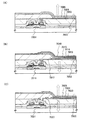
本発明の表示装置の作製方法について説明する。はじめに、表示装置の一形態とし液晶表示装置を用いて説明する。図1乃至図8に、駆動回路121に形成される薄膜トランジスタの断面図と、画素部122に形成される薄膜トランジスタの断面図を示す。なお、微結晶半導体膜を有する薄膜トランジスタはp型よりもn型の方が、移動度が高いので駆動回路に用いるのにより適しているが、本発明では、薄膜トランジスタはn型であってもp型であってもどちらでも良い。いずれの極性の薄膜トランジスタを用いる場合でも、同一の基板上に形成する薄膜トランジスタを全て同じ極性にそろえておくことが、工程数を抑えるためにも望ましい。ここでは、n型の薄膜トランジスタの作製方法について示す。
(Embodiment 1)
A method for manufacturing a display device of the present invention will be described. First, an example of a display device will be described using a liquid crystal display device. 1 to 8 illustrate a cross-sectional view of a thin film transistor formed in the driver circuit 121 and a cross-sectional view of a thin film transistor formed in the pixel portion 122. FIG. Note that a thin film transistor including a microcrystalline semiconductor film is more suitable for use in a driver circuit because the n-type has higher mobility than the p-type. Or either. Regardless of which thin film transistor is used, it is desirable to keep all thin film transistors formed on the same substrate to have the same polarity in order to reduce the number of steps. Here, a method for manufacturing an n-type thin film transistor is described.
図1(A)に示すように、基板50上にゲート電極51a、51bを形成する。基板50は、バリウムホウケイ酸ガラス、アルミノホウケイ酸ガラス、若しくはアルミノシリケートガラスなど、フュージョン法やフロート法で作製される無アルカリガラス基板、セラミック基板の他、本作製工程の処理温度に耐えうる耐熱性を有するプラスチック基板等を用いることができる。また、ステンレス合金などの金属基板の表面に絶縁膜を設けた基板を適用しても良い。基板50の大きさは、320mm×400mm、370mm×470mm、550mm×650mm、600mm×720mm、680mm×880mm、730mm×920mm、1000mm×1200mm、1100mm×1250mm、1150mm×1300mm、1500mm×1800mm、1900mm×2200mm、2160mm×2460mm、2400mm×2800mm、又は2850mm×3050mm等を用いることができる。
As shown in FIG. 1A,
ゲート電極51a、51bは、チタン、モリブデン、クロム、タンタル、タングステン、アルミニウムなどの金属材料またはその合金材料を用いて形成する。ゲート電極51a、51bは、スパッタリング法や真空蒸着法で基板50上に導電膜を形成し、当該導電膜上にフォトリソグラフィ技術またはインクジェット法によりマスクを形成し、当該マスクを用いて導電膜をエッチングすることで、形成することができる。また、銀、金、銅などの導電性ナノペーストを用いてインクジェット法により吐出し焼成して、ゲート電極51a、51bを形成することができる。なお、ゲート電極51a、51bの密着性向上のために、上記金属材料の窒化物膜を、基板50及びゲート電極51a、51bの間に設けてもよい。
The
なお、ゲート電極51a、51b上には、絶縁膜や半導体膜や配線を形成するので、段切れ防止のため端部がテーパー状になるように加工することが望ましい。また、図示しないがこの工程でゲート電極に接続する配線も同時に形成することができる。
Note that since an insulating film, a semiconductor film, and a wiring are formed over the
次に、ゲート電極51a、51b上に、ゲート絶縁膜52、微結晶半導体膜53、非晶質半導体膜54を順に形成する。なお、少なくとも、ゲート絶縁膜52、微結晶半導体膜53、及び非晶質半導体膜54を連続的に形成することが好ましい。ゲート絶縁膜52、微結晶半導体膜53、及び非晶質半導体膜54を大気に触れさせることなく連続成膜することで、大気成分や大気中に浮遊する汚染不純物元素に汚染されることなく各積層界面を形成することができるので、薄膜トランジスタ特性のばらつきを低減することができる。
Next, a
ゲート絶縁膜52は、CVD法やスパッタリング法等を用いて、酸化珪素膜、窒化珪素膜、酸化窒化珪素膜、または窒化酸化珪素膜の単層若しくは積層で形成することができる。また、基板側から酸化珪素膜または酸化窒化珪素膜と、窒化珪素膜または窒化酸化珪素膜との順に積層して形成することができる。また、基板側から窒化珪素膜または窒化酸化珪素膜と、酸化珪素膜または酸化窒化珪素膜と、窒化珪素膜または窒化酸化珪素膜との順に積層して形成することができる。更には、周波数が1GHz以上のマイクロ波プラズマCVD装置を用いてゲート絶縁膜52を形成することが好ましい。マイクロ波プラズマCVD装置で形成した酸化窒化珪素膜、窒化酸化珪素膜は、耐圧が高く、後に形成される薄膜トランジスタの信頼性を高めることができる。
The
なお、酸化窒化珪素膜とは、その組成として、窒素よりも酸素の含有量が多いものであって、ラザフォード後方散乱法(RBS:Rutherford Backscattering Spectrometry)及び水素前方散乱法(HFS:Hydrogen Forward Scattering)を用いて測定した場合に、濃度範囲として酸素が50〜70原子%、窒素が0.5〜15原子%、珪素が25〜35原子%、水素が0.1〜10原子%の範囲で含まれるものをいう。また、窒化酸化珪素膜とは、その組成として、酸素よりも窒素の含有量が多いものであって、RBS及びHFSを用いて測定した場合に、濃度範囲として酸素が5〜30原子%、窒素が20〜55原子%、珪素が25〜35原子%、水素が10〜30原子%の範囲で含まれるものをいう。但し、酸化窒化珪素または窒化酸化珪素を構成する原子の合計を100原子%としたとき、窒素、酸素、珪素及び水素の含有比率が上記の範囲内に含まれるものとする。 Note that the silicon oxynitride film has a composition that contains more oxygen than nitrogen, and includes Rutherford Backscattering (RBS) and Hydrogen Forward Scattering (HFS). As a concentration range, oxygen is included in the range of 50 to 70 atomic%, nitrogen is 0.5 to 15 atomic%, silicon is 25 to 35 atomic%, and hydrogen is 0.1 to 10 atomic%. Means what In addition, the silicon nitride oxide film has a nitrogen content higher than that of oxygen as a composition. When measured using RBS and HFS, the concentration range of oxygen is 5 to 30 atomic%, nitrogen. Is contained in the range of 20 to 55 atomic%, silicon of 25 to 35 atomic%, and hydrogen of 10 to 30 atomic%. However, when the total number of atoms constituting silicon oxynitride or silicon nitride oxide is 100 atomic%, the content ratio of nitrogen, oxygen, silicon, and hydrogen is included in the above range.
微結晶半導体膜53は、非晶質と結晶構造(単結晶、多結晶を含む)の中間的な構造の半導体を含む膜である。この半導体は、自由エネルギー的に安定な第3の状態を有する半導体であって、短距離秩序を持ち格子歪みを有する結晶質なものであり、その粒径を0.5〜20nmとして非単結晶半導体中に分散させて存在せしめることが可能である。また、未結合手(ダングリングボンド)を終端するため水素またはハロゲンを少なくとも1原子%またはそれ以上含ませている。さらに、ヘリウム、アルゴン、クリプトン、ネオンなどの希ガス元素を含ませて格子歪みをさらに助長させることで、安定性が増し良好な微結晶半導体膜が得られる。このような微結晶半導体膜に関する記述は、例えば、米国特許4,409,134号で開示されている。
The
この微結晶半導体膜は、周波数が数十MHz〜数百MHzの高周波プラズマCVD装置、または周波数が1GHz以上のマイクロ波プラズマCVD装置により形成することができる。代表的には、SiH4、Si2H6などの水素化珪素、SiH2Cl2、SiHCl3、SiCl4、SiF4などのハロゲン化珪素を水素で希釈して形成することができる。また、水素化珪素またはハロゲン化珪素と、水素とに加え、ヘリウム、アルゴン、クリプトン、ネオンから選ばれた一種または複数種の希ガス元素で希釈して微結晶半導体膜を形成することができる。これらのときの水素化珪素に対して水素の流量比を5倍以上200倍以下、好ましくは50倍以上150倍以下、更に好ましくは100倍とする。 This microcrystalline semiconductor film can be formed by a high-frequency plasma CVD apparatus having a frequency of several tens to several hundreds of MHz or a microwave plasma CVD apparatus having a frequency of 1 GHz or more. Typically, silicon hydrides such as SiH 4 and Si 2 H 6 and silicon halides such as SiH 2 Cl 2 , SiHCl 3 , SiCl 4 , and SiF 4 can be formed by diluting with hydrogen. In addition to silicon hydride or silicon halide, and hydrogen, the microcrystalline semiconductor film can be formed by dilution with one or more kinds of rare gas elements selected from helium, argon, krypton, and neon. The flow rate ratio of hydrogen to silicon hydride at these times is 5 to 200 times, preferably 50 to 150 times, and more preferably 100 times.
微結晶半導体膜53は、1nm以上20nm以下、好ましくは10nm以上20nm以下で形成する。微結晶半導体膜53は、非晶質半導体膜54を微結晶化するための種結晶であるため、膜厚を厚く成膜する必要は無い。
The
また、微結晶半導体膜53を形成する前に、ゲート絶縁膜の表面を水素、窒素、ハロゲン、希ガスのいずれかのプラズマで処理してゲート絶縁膜の表面を凹凸としてもよい。このようにすることで、ゲート絶縁膜と微結晶半導体膜との界面での格子歪を低減することが可能である。
Alternatively, before the
非晶質半導体膜54は、SiH4、Si2H6、SiH2Cl2、SiHCl3、SiCl4、SiF4などの水素化珪素またはハロゲン化珪素を用いて、プラズマCVD法により形成することができる。また、上記水素化珪素に、ヘリウム、アルゴン、クリプトン、ネオンから選ばれた一種または複数種の希ガス元素で希釈して非晶質半導体膜を形成することができる。これらのときの水素化珪素またはハロゲン化珪素、若しくは水素化珪素またはハロゲン化珪素と希ガスとで非晶質半導体膜を形成することで、非晶質半導体膜の成膜速度を高めることができる。
The
非晶質半導体膜54は、50nm以上200nm以下、好ましくは100nm以上15nm以下で形成する。
The
また、水素化珪素中に、CH4、C2H6などの炭化物気体を混入させて、エネルギーバンド幅を1.5〜2.4eVに調整してもよい。または、水素化珪素中に、GeH4、GeF4などのゲルマニウム化気体を混入させて、エネルギーバンド幅を0.9〜1.1eVに調節しても良い。 Further, a carbide gas such as CH 4 or C 2 H 6 may be mixed in silicon hydride to adjust the energy bandwidth to 1.5 to 2.4 eV. Alternatively, germanium gas such as GeH 4 and GeF 4 may be mixed in silicon hydride to adjust the energy bandwidth to 0.9 to 1.1 eV.
また、後に形成される微結晶半導体膜は、価電子制御を目的とした不純物元素を意図的に添加しないときに弱いn型の電気伝導性を示すので、薄膜トランジスタのチャネル形成領域として機能する微結晶半導体膜に対しては、p型を付与する不純物元素を、非晶質半導体膜の成膜時に、或いは成膜後に添加することで、しきい値制御をすることが可能となる。p型を付与する不純物元素としては、代表的には硼素であり、B2H6、BF3などの不純物気体を1ppm〜1000ppm、好ましくは1〜100ppmの割合で水素化珪素に混入させると良い。そしてボロンの濃度を、例えば1×10¹⁴〜6×10¹⁶/cm3とすると良い。 In addition, since a microcrystalline semiconductor film formed later exhibits weak n-type conductivity when an impurity element for the purpose of valence electron control is not intentionally added, a microcrystal functioning as a channel formation region of a thin film transistor The threshold value can be controlled by adding an impurity element imparting p-type conductivity to the semiconductor film during or after the formation of the amorphous semiconductor film. The impurity element imparting p-type is typically boron, and an impurity gas such as B 2 H 6 or BF 3 may be mixed into silicon hydride at a rate of 1 ppm to 1000 ppm, preferably 1 to 100 ppm. . The concentration of boron is preferably 1 × 10 14 to 6 × 10 16 / cm 3 , for example.
また、非晶質半導体膜の酸素濃度を、5×10¹⁸/cm3以下、1×1018/cm3以下、窒素及び炭素の濃度それぞれを1×1019/cm3以下とすることが好ましい。酸素、窒素、及び炭素が微結晶半導体膜に混入する濃度を低減することで、後に形成される微結晶半導体膜がn型になることを防止することができる。 The oxygen concentration of the amorphous semiconductor film is preferably 5 × 10 18 / cm 3 or less, 1 × 10 18 / cm 3 or less, and the concentrations of nitrogen and carbon are each 1 × 10 19 / cm 3 or less. . By reducing the concentration of oxygen, nitrogen, and carbon mixed in the microcrystalline semiconductor film, the microcrystalline semiconductor film formed later can be prevented from becoming n-type.
次に、非晶質半導体膜54に含まれる水素を除くために450℃以上550℃以下で1時間以上12時間以下、好ましくは1時間以上3時間以下の加熱を行う。当該加熱により非晶質半導体膜54に含まれる水素を脱離させることが可能であるため、のちにレーザビームの照射により水素ガスが非晶質半導体膜から噴出することを防ぐことができる。
Next, in order to remove hydrogen contained in the
次に、非晶質半導体膜54に、エネルギー分布のプロファイルがなだらかなレーザビーム、即ち単位面積当たりのエネルギーが低いレーザビームを照射して、非晶質半導体膜を微結晶化させて、図1(B)に示すように、ゲート絶縁膜52上に微結晶半導体膜55を形成する。
Next, the
エネルギー分布のプロファイルがなだらかなレーザビームは、ビーム形状を拡大することが可能なビームエキスパンダや、エネルギー分布を均一化するビームホモジナイザなどの光学系を、レーザ発振器と、基板上に形成される非晶質半導体膜との間に設け、当該光学系を介して非晶質半導体膜に照射する。さらには、ビームエキスパンダ及びビームホモジナイザを、レーザ発振器と基板上に形成される非晶質半導体膜との間に設け、当該光学系を介して非晶質半導体膜に照射することができる。また、レーザ発振器と、非晶質半導体膜54の間に、レーザビームを散乱または吸収するすりガラス40を設け、すりガラス40を介して非晶質半導体膜54にレーザビーム41を照射することが可能である(図1(A)参照)。
A laser beam with a gentle energy distribution profile uses a laser expander and an optical system such as a beam expander that can expand the beam shape and a beam homogenizer that makes the energy distribution uniform. It is provided between the crystalline semiconductor film and the amorphous semiconductor film is irradiated through the optical system. Further, a beam expander and a beam homogenizer can be provided between the laser oscillator and the amorphous semiconductor film formed over the substrate, and the amorphous semiconductor film can be irradiated through the optical system. A
ビームエキスパンダは、凹シリンドリカルレンズと凸シリンドリカルレンズを組み合わせたものであり、これにより、レーザ発振器から放射されるレーザビームのビーム幅を広げることができる。このため、単位面積当たりのエネルギーが低いレーザビームとなる。 The beam expander is a combination of a concave cylindrical lens and a convex cylindrical lens, whereby the beam width of the laser beam emitted from the laser oscillator can be widened. For this reason, it becomes a laser beam with low energy per unit area.
また、ビームホモジナイザは、例えばマルチモードで発振してレーザビームのエネルギー分布を均一化するためのものである。または、凹シリンドリカルレンズアレイと、凸シリンドリカルレンズアレイと、凸シリンドリカルレンズを組み合わせたものである。ビームホモジナイザにより、レーザ発振器から放射されるレーザビームにおいて、基板の薄膜堆積表面と平行な方向のエネルギー密度分布を均一化することができる。 The beam homogenizer is for, for example, oscillating in a multi-mode to uniformize the energy distribution of the laser beam. Alternatively, a concave cylindrical lens array, a convex cylindrical lens array, and a convex cylindrical lens are combined. By the beam homogenizer, the energy density distribution in the direction parallel to the thin film deposition surface of the substrate can be made uniform in the laser beam emitted from the laser oscillator.
ここで、エネルギー分布のプロファイルがなだらかである線状のレーザビームを照射することが可能な光学系を図11に示す。 Here, FIG. 11 shows an optical system capable of irradiating a linear laser beam having a gentle energy distribution profile.
図11(A)は、エネルギー分布のプロファイルがなだらかである線状のレーザビームを照射することが可能な光学系の側面図であり、レーザビームの短軸方向のエネルギーのプロファイルをなだらかにする。また、図11(B)は、エネルギー分布のプロファイルがなだらかである線状のレーザビームを照射することが可能な光学系の平面図であり、レーザビームの長軸方向のエネルギーのプロファイルをなだらかにする。 FIG. 11A is a side view of an optical system capable of irradiating a linear laser beam having a gentle energy distribution profile, and smoothes the energy profile in the minor axis direction of the laser beam. FIG. 11B is a plan view of an optical system capable of irradiating a linear laser beam having a gentle energy distribution profile. The energy profile in the major axis direction of the laser beam is gently changed. To do.
図11(A)及び図11(B)に示すように、レーザ発振器401から発振されたレーザビーム400は、ビームエキスパンダ402でレーザビームの長さ(長軸方向の長さ)及び幅(短軸方向の長さ)を拡大する。ビームエキスパンダ402はレーザ発振器401側が凹である球面レンズ402a、レーザ発振器401側に凸である球面レンズ402bで構成される。
As shown in FIGS. 11A and 11B, a
なお、レーザ発振器401及びビームエキスパンダ402の間に、レーザビームの強度を適切に減衰させるアッテネータを設置してもよい。アッテネータを設置することによってレーザビームのエネルギー強度を制御できる。
An attenuator that appropriately attenuates the intensity of the laser beam may be provided between the
ビームエキスパンダ402を透過したレーザビームは、ビームホモジナイザ403でレーザビームの長軸方向のエネルギーが均一化される。ビームホモジナイザ403は、レーザ発振器401側に凸であるシリンドリカルレンズアレイ403a、レーザ発振器401側が凸であるシリンドリカルレンズアレイ403b、及びレーザ発振器401側が凸であるシリンドリカルレンズ404で構成される。シリンドリカルレンズアレイ403a、403bによりレーザビームの長軸方向が分割され、均一化される。
The laser beam that has passed through the
ビームホモジナイザ403を透過したレーザビームは、ビームホモジナイザ405でレーザビームの短軸方向のエネルギーが均一化される。ビームホモジナイザ405は、レーザ発振器401側が凹であるシリンドリカルレンズアレイ405a、レーザ発振器401側が凸であるシリンドリカルレンズアレイ405b、及びレーザ発振器401側が凸であるシリンドリカルレンズ406で構成される。シリンドリカルレンズアレイ405a、405bによりレーザビームの短軸方向が分割される。また、シリンドリカルレンズ406によって、エネルギーが均一化される。
The laser beam that has passed through the
ビームホモジナイザ405を透過したレーザビームは、ダブレットシリンドリカルレンズ407で集光される。この結果、基板50上に形成される非晶質半導体膜に、矩形状または線状であり、エネルギー分布のプロファイルがなだらかなレーザビームを照射することができる。ダブレットシリンドリカルレンズ407は、レーザ発振器401側が凸で基板50側が凹であるシリンドリカルレンズ407aと、レーザ発振器401側が凸で基板50側が凸であるシリンドリカルレンズアレイ407bとで構成される。
The laser beam that has passed through the
なお、長軸側のレーザビームの端部はエネルギー分布の均一性が低いため、基板50とダブレットシリンドリカルレンズ407の間に、スリット408を設けることが好ましい。当該スリットにより、長軸側のレーザビームの端部を除いた均一性の高いレーザビームを基板50上の非晶質半導体膜上に照射することができる。なお、レーザビームがスリットの裏側に回りこむのを避けるため、スリット408はなるべく基板50に近い領域に設けることが好ましい。
Note that it is preferable to provide a
ビームホモジナイザ405のシリンドリカルレンズ406及びダブレットシリンドリカルレンズ407の距離を距離bとし、ダブレットシリンドリカルレンズ407及び基板50の非晶質半導体膜の距離を距離aとすると、レーザビームの照射面でのビーム幅の倍率はおよそb/a倍である。b/aの値を大きくすると、レーザビーム幅の倍率が大きくなり、レーザビームの幅は絞られ狭くなる。一方b/aの値を小さくすると、レーザビーム幅の倍率が小さくなり、レーザビーム幅はより広くなる。即ち、このため、ビームホモジナイザ405のシリンドリカルレンズ406の位置を基板50側にずらすことで、距離bが小さくなり、基板50上の非晶質半導体膜表面において、レーザビームの幅が広くなる。または、ダブレットシリンドリカルレンズ407の位置をレーザ発振器401側にずらすことにより、距離bが小さくなり、距離aが大きくなるため、基板50上の非晶質半導体膜表面において、レーザビームの幅が広くなる。または、基板50の位置をダブレットシリンドリカルレンズ407から遠ざけることにより、距離aが大きくなり、基板50上の非晶質半導体膜表面において、レーザビームの幅が広くなる。この結果、エネルギー分布のプロファイルがなだらかであり幅の広いレーザビームを非晶質半導体膜に照射することができる。
When the distance between the
矩形状または線状のレーザビームをスキャンする、もしくは基板をスキャンすることにより、広い面積の基板を処理することができる。なお、レーザ発振器135から発振されたレーザビームの光路を変更させるため、レーザ発振器135及び基板50の間に光路を変更させる光学系、代表的にはミラーを設けることができる。
By scanning a rectangular or linear laser beam or scanning a substrate, a substrate having a large area can be processed. In order to change the optical path of the laser beam oscillated from the laser oscillator 135, an optical system that changes the optical path, typically a mirror, can be provided between the laser oscillator 135 and the
また、すりガラス40は、石英ガラスの表面に微小な凹凸を形成し、光を一部吸収または散乱させる。もしくは、石英ガラスの表面に半透過膜を形成し、光を一部吸収または散乱させる。この結果、すりガラスによりレーザビーム41の焦点を非晶質半導体膜からずらすことが可能であり、レーザビームのエネルギー分布のプロファイルがブロードとなる。
The
レーザビームを発振するレーザ発振器としては、パルス発振することが可能なレーザ発振器を用いることができる。また、レーザ波長は、半導体膜に効率よくレーザビームが吸収されるように可視〜紫外領域(800nm以下)、好ましくは紫外領域(400nm以下)とする。レーザ発振器としては、KrF、ArF、XeCl、XeF等のエキシマレーザ発振器、N2、He、He−Cd、Ar、He−Ne、HF等の気体レーザ発振器、YAG、GdVO4、YVO4、YLF、YAlO3、ScO3、Lu2O3、Y2O3などの結晶にCr、Nd、Er、Ho、Ce、Co、Ti、Yb、又はTmをドープした結晶を使った固体レーザ発振器、ヘリウムカドミウムレーザ等の金属蒸気レーザ発振器等を用いることができる。なお、固体レーザ発振器においては、基本波の第3高調波〜第5高調波を適用するのが好ましい。 As a laser oscillator that oscillates a laser beam, a laser oscillator capable of pulse oscillation can be used. The laser wavelength is in the visible to ultraviolet region (800 nm or less), preferably in the ultraviolet region (400 nm or less) so that the semiconductor film can efficiently absorb the laser beam. As the laser oscillator, excimer laser oscillators such as KrF, ArF, XeCl, and XeF, gas laser oscillators such as N 2 , He, He—Cd, Ar, He—Ne, and HF, YAG, GdVO 4 , YVO 4 , YLF, Solid-state laser oscillator using helium cadmium using a crystal doped with Cr, Nd, Er, Ho, Ce, Co, Ti, Yb, or Tm on a crystal such as YAlO 3 , ScO 3 , Lu 2 O 3 , Y 2 O 3 A metal vapor laser oscillator such as a laser can be used. In the solid-state laser oscillator, it is preferable to apply the third to fifth harmonics of the fundamental wave.
代表的には、レーザビームとして波長400nm以下のエキシマレーザビームや、YAGレーザの第3高調波、第4高調波を用いる。 Typically, an excimer laser beam having a wavelength of 400 nm or less or a third harmonic or a fourth harmonic of a YAG laser is used as the laser beam.
結晶化の条件は実施者が適宣選択するものであるが、エキシマレーザを用いる場合はパルス発振周波数1Hz以上10MHz未満、好ましくは100Hz〜10kHzとし、レーザエネルギーを0.1〜0.3J/cm2(代表的には0.15〜0.25J/cm2、更に好ましくは0.15J/cm2以上0.2J/cm2未満)とする。また、YAGレーザを用いる場合にはその第3高調波を用いパルス発振周波数1Hz以上10MHz未満とし、レーザエネルギーを0.1〜0.3J/cm2(代表的には0.15〜0.25J/cm2、更に好ましくは0.15J/cm2以上0.2J/cm2未満)とすると良い。 The crystallization conditions are appropriately selected by the practitioner. When an excimer laser is used, the pulse oscillation frequency is 1 Hz or more and less than 10 MHz, preferably 100 Hz to 10 kHz, and the laser energy is 0.1 to 0.3 J / cm. 2 (typically 0.15~0.25J / cm 2, more preferably 0.15 J / cm 2 or more 0.2 J / cm less than 2) and. When a YAG laser is used, the third harmonic is used and the pulse oscillation frequency is set to 1 Hz or more and less than 10 MHz, and the laser energy is set to 0.1 to 0.3 J / cm 2 (typically 0.15 to 0.25 J). / cm 2, more preferably may be set to be 0.15 J / cm 2 or more 0.2 J / cm less than 2).
ここで、従来のエキシマレーザビームと、本実施の形態のエキシマレーザビームのエネルギーのプロファイルについて、図12を用いて説明する。 Here, the energy profiles of the conventional excimer laser beam and the excimer laser beam of this embodiment will be described with reference to FIG.
図12(A)は、従来のELAに用いるレーザビームのエネルギー分布のプロファイルを示し、横軸に走査距離、縦軸にエネルギー強度を示す。従来のELAに用いるレーザビームのエネルギー分布のプロファイル147a〜147dは、幅数百μm、代表的には300〜600μmであり、プロファイルのピークが急峻である。即ち、エネルギー分布の勾配の絶対値が大きいピークである。このようなレーザビームを85〜95%の割合で重ね合わせることにより、即ち、レーザビームまたは基板をずらしながらパルス発振のレーザビームを照射することで、非晶質半導体膜を結晶化している。しかしながら、レーザビームのエネルギーのピークにおいて、エネルギー強度のばらつきが大きい。例えば、プロファイル147cはプロファイル147a、147b、147d、147eと比較して、強度が高く、プロファイル147eはプロファイル147a〜147dと比較して、強度が低く、エネルギー強度が異なる。このため、このようなレーザビームの照射により形成された結晶性半導体膜は、結晶粒の大きさのばらつきが大きい。また、レーザビームのエネルギー強度のプロファイルが急峻であればあるほど、大気圧下でのレーザビームの照射により、形成される結晶性半導体膜の表面に凹凸(リッジ)ができやすく、結晶性半導体膜の膜厚の均一性が低くなる。
FIG. 12A shows an energy distribution profile of a laser beam used in a conventional ELA, where the horizontal axis indicates the scanning distance and the vertical axis indicates the energy intensity. The
図12(B)は、本実施の形態で用いるレーザビームのエネルギー分布のプロファイルを示し、横軸に走査距離、縦軸にエネルギー強度を示す。本実施の形態で用いるレーザビームのエネルギー分布のプロファイル148a〜148cは、幅数mm、代表的には1〜5mmであり、曲線がなだらかなピークである。即ち、エネルギー分布のプロファイルの勾配の絶対値が小さいピークである。また、エネルギー強度が低いため、エネルギー強度のばらつきが小さい。例えば、プロファイル148cは、プロファイル148a、148b、と比較して、強度が高いが、そもそもエネルギー強度が低いため、エネルギー強度の差はそれほど大きくない。このようなレーザビームを重ね合わせることにより、即ち、レーザビームまたは基板をずらしながらパルス発振のレーザビームを照射することで、非晶質半導体膜全体に均一なエネルギーが照射される。このため、このようなレーザビームの照射により形成された微結晶半導体膜は、結晶粒径のばらつきも少ない。また膜厚の均一性が高くなる。なお、エネルギー分布の勾配の絶対値が小さいピークとしては、エネルギー分布のプロファイルの勾配の絶対値がゼロ、即ち、トップフラットな形状でもよい。
FIG. 12B shows a profile of the energy distribution of the laser beam used in this embodiment, where the horizontal axis indicates the scanning distance and the vertical axis indicates the energy intensity. The
非晶質半導体膜の下地として微結晶半導体膜が形成されているため、微結晶半導体膜が結晶成長の種(トリガー)となって結晶成長が行われるため、縦方向、即ち基板に対して法線方向に結晶成長する。ここで、図1(B)のゲート電極51a付近の拡大図を図10に示す。図10に示すように、レーザビームが照射され結晶化された微結晶半導体膜55は、基板50表面に対して法線方向に結晶粒界55aが形成されており、柱状の微結晶粒を含む。また、非晶質半導体も含む。
Since the microcrystalline semiconductor film is formed as a base of the amorphous semiconductor film, the microcrystalline semiconductor film is used as a seed of crystal growth (trigger) and crystal growth is performed. Crystals grow in the line direction. Here, an enlarged view of the vicinity of the
なお、ゲート絶縁膜と微結晶半導体膜の界面においては、格子歪が生じ、微結晶化せず、数nmの非晶質半導体層が形成される。しかしながら、プロファイルのなだらかなレーザビームを微結晶半導体膜上に形成された非晶質半導体膜に照射すると、微結晶半導体膜の上部に形成される非晶質半導体膜と同様に、ゲート絶縁膜と微結晶半導体膜の界面にある非晶質半導体層の結晶性を高めることができる。このため、チャネル形成領域として機能する微結晶半導体膜とゲート絶縁膜との界面特性を向上させることが可能である。逆スガタ薄膜トランジスタがオンの場合、キャリアは微結晶半導体膜においてゲート絶縁膜との界面近傍を流れるため、当該領域の結晶性を高めることにより、薄膜トランジスタの特性を向上させると共に、ばらつきを低減することができる。 Note that lattice distortion occurs at the interface between the gate insulating film and the microcrystalline semiconductor film, and the amorphous semiconductor layer with a thickness of several nanometers is formed without microcrystallization. However, when an amorphous semiconductor film formed over the microcrystalline semiconductor film is irradiated with a laser beam having a gentle profile, the gate insulating film and the amorphous semiconductor film formed over the microcrystalline semiconductor film are formed. The crystallinity of the amorphous semiconductor layer at the interface of the microcrystalline semiconductor film can be increased. Therefore, the interface characteristics between the microcrystalline semiconductor film functioning as a channel formation region and the gate insulating film can be improved. When the inversely thin film transistor is on, carriers flow in the vicinity of the interface with the gate insulating film in the microcrystalline semiconductor film; thus, improving the crystallinity of the region can improve the characteristics of the thin film transistor and reduce variation. it can.
また、レーザビームのエネルギーを低くすることが可能であるため、照射速度も早く、タクトが良いと共に、電力が低くなりコストの削減が可能である。 Further, since the energy of the laser beam can be reduced, the irradiation speed is high, the tact is good, the power is reduced, and the cost can be reduced.
レーザビームのエネルギー強度と結晶粒径の関係について、図12(C)を用いて説明する。レーザビームのエネルギー強度が低い場合、代表的にはレーザビームのエネルギーが0.1mJ/cm2以上0.3mJ/cm2未満(代表的には0.15J/cm2以上0.25J/cm2以下、更に好ましくは0.15J/cm2以上0.2J/cm2未満)の場合、領域155においては、粒径が0.5nm以上50nm以下、好ましくは0.5nm以上20nm以下の微結晶が形成される。微結晶粒は、エネルギーの変化に対する結晶粒の成長が少ない。
A relationship between the energy intensity of the laser beam and the crystal grain size will be described with reference to FIG. When the energy intensity of the laser beam is low, the energy of the laser beam is typically 0.1 mJ / cm 2 or more and less than 0.3 mJ / cm 2 (typically 0.15 J / cm 2 or more and 0.25 J / cm 2 Or less, more preferably 0.15 J / cm 2 or more and less than 0.2 J / cm 2 ), in the
領域155よりエネルギー強度が高い場合、代表的にはレーザビームのエネルギーが0.3mJ/cm2以上0.5mJ/cm2の場合、領域156では、粒径が50nmより大きく10μm以下、好ましくは100nm以上1μm以下である。この領域においては、エネルギーの増加に伴って結晶粒が成長し、大きな結晶粒となる。更に、エネルギー強度が高い領域157では、粒径が0.5nm以上50nm以下、好ましくは0.5nm以上20nm以下の微結晶が形成される。すなわち、領域155のように結晶粒が小さくなり、且つエネルギーの変化に関わらず結晶粒の大きさが変化しない。しかしながら、領域157のようなエネルギーのレーザビームは、エネルギーが高いため、膜剥れが起き易い。また、レーザビームのエネルギーが高いため、照射速度が遅くなりタクトが悪いと共に、高い電力が必要となりコストが高くなる。領域156のようなエネルギーのレーザビームは、結晶粒の大きさがレーザビームのエネルギーの変動に左右されやすく、結晶粒径のばらつきが生じやすい。このため、領域155のように、レーザビームの変動に対応して結晶粒の大きさの変動が少ないエネルギーのレーザビームを照射することが好ましい。このようなレーザビームは、レーザ発振器のパワーを制御する、またはレーザビームの一部を吸収または散乱する光学系を介することが好ましい。
When the energy intensity is higher than that of the
本実施の形態では、成膜速度の遅い微結晶半導体膜及び成膜速度の早い非晶質半導体膜を連続成膜し、非晶質半導体膜にエネルギー分布のプロファイルがなだらかであるレーザビームを照射して、微結晶半導体膜を形成するため、成膜速度の遅い微結晶半導体膜のみを成膜するよりも、スループットを向上させることができる。 In this embodiment mode, a microcrystalline semiconductor film with a low film formation rate and an amorphous semiconductor film with a high film formation rate are continuously formed, and the amorphous semiconductor film is irradiated with a laser beam having a gentle energy distribution profile. Thus, since the microcrystalline semiconductor film is formed, the throughput can be improved as compared with the case where only the microcrystalline semiconductor film having a low deposition rate is formed.
ここで、図1(A)に示すゲート絶縁膜52から非晶質半導体膜54を連続成膜ことが可能なマイクロ波プラズマCVD装置について、図13を用いて示す。図13はマイクロ波プラズマCVD装置の上断面を示す模式図であり、共通室1120の周りに、ロード室1110、アンロード室1115、反応室(1)〜反応室(4)1111〜1114を備えた構成となっている。共通室1200と各室の間にはゲートバルブ1122〜1127が備えられ、各室で行われる処理が、相互に干渉しないように構成されている。基板1130はロード室1110、アンロード室1115のカセット1128、1129に装填され、共通室1120の搬送手段1121により反応室(1)〜反応室(4)1111〜1114へ運ばれる。この装置では、堆積膜種ごとに反応室をあてがうことが可能であり、複数の異なる被膜を大気に触れさせることなく連続して形成することができる。
Here, a microwave plasma CVD apparatus capable of continuously forming an
反応室(1)〜反応室(3)それぞれにおいて、ゲート絶縁膜52、微結晶半導体膜53、及び非晶質半導体膜54を積層形成する。この場合は、原料ガスの切り替えにより異なる種類の膜を連続的に複数積層することができる。このように、複数のチャンバが接続されたマイクロ波プラズマCVD装置で、同時にゲート絶縁膜52、微結晶半導体膜53、及び非晶質半導体膜54を成膜することができるため、量産性を高めることができる。また、ある反応室がメンテナンスやクリーニングを行っていても、残りの反応室において成膜処理が可能となり、成膜のタクトを向上させることができる。また、大気成分や大気中に浮遊する汚染不純物元素に汚染されることなく各積層界面を形成することができるので、薄膜トランジスタ特性のばらつきを低減することができる。
In each of the reaction chamber (1) to the reaction chamber (3), the
また、ゲート絶縁膜を酸化珪素膜または酸化窒化珪素膜と、窒化珪素膜または窒化酸化珪素膜との2層で形成する場合、反応室を4つ設け、反応室(1)で、ゲート絶縁膜の酸化珪素膜または酸化窒化珪素膜を形成し、反応室(2)で、ゲート絶縁膜の窒化珪素膜または窒化酸化珪素膜を形成し、反応室(3)で、微結晶半導体膜を形成し、反応室(4)で非晶質半導体膜54を形成してもよい。このとき、各反応室の内壁を成膜する種類の膜でコーティングすることが好ましい。このような構成のマイクロ波プラズマCVD装置を用いれば、各反応室で一種類の膜を成膜することが可能であり、且つ大気に曝すことなく連続して形成することができるため、前に成膜した膜の残留物や大気に浮遊する不純物元素に汚染されることなく、各積層界面を形成することができる。
In the case where the gate insulating film is formed of two layers of a silicon oxide film or a silicon oxynitride film and a silicon nitride film or a silicon nitride oxide film, four reaction chambers are provided, and the gate insulating film is formed in the reaction chamber (1). A silicon oxide film or a silicon oxynitride film is formed, a silicon nitride film or a silicon nitride oxide film as a gate insulating film is formed in the reaction chamber (2), and a microcrystalline semiconductor film is formed in the reaction chamber (3). The
さらには、マイクロ波発生装置と共に高周波発生装置を設け、ゲート絶縁膜及び微結晶半導体膜をマイクロ波プラズマCVD法で形成し、非晶質半導体膜を高周波プラズマCVD法で形成してもよい。 Further, a high frequency generator may be provided together with the microwave generator, the gate insulating film and the microcrystalline semiconductor film may be formed by a microwave plasma CVD method, and the amorphous semiconductor film may be formed by a high frequency plasma CVD method.
なお、図13に示すマイクロ波プラズマCVD装置には、ロード室及びアンロード室が別々に設けられているが、一つとしロード/アンロード室とでもよい。また、マイクロ波プラズマCVD装置に予備室を設けてもよい。予備室で基板を予備加熱することで、各反応室において成膜までの加熱時間を短縮することが可能であるため、スループットを向上させることができる。 In the microwave plasma CVD apparatus shown in FIG. 13, a load chamber and an unload chamber are provided separately, but a single load / unload chamber may be used. Further, a spare chamber may be provided in the microwave plasma CVD apparatus. By preheating the substrate in the preliminary chamber, the heating time until film formation in each reaction chamber can be shortened, so that the throughput can be improved.
図14はこのようなマイクロ波プラズマCVD装置の一つの反応室の構成を詳細に説明するものである。なお、ガス供給部182及びマイクロ波発生装置184は反応室の外に設けられる。
FIG. 14 explains in detail the structure of one reaction chamber of such a microwave plasma CVD apparatus. Note that the
マイクロ波発生装置184は、周波数が1GHz以上、代表的には2.45GHzまたは8.3GHzのマイクロ波を供給する。なお、本発明においては、マイクロ波発生装置184を複数有することで、安定な大面積のプラズマを生成することが可能である。このため、一辺が600mmを超える基板、特に一辺が1000mmを超える大面積基板においても、均一性の高い膜を成膜する事が可能であり、且つ成膜速度を高めることができる。
The
処理容器180は、密閉構造により内部を減圧に保持できる構成となっている。処理容器180及び天板187は、表面がアルミナ、酸化珪素、フッ素樹脂のいずれかの絶縁膜で覆われた金属、例えばアルミニウムを含む合金で形成される。また、取り付け具188は金属、例えばアルミニウムを含む合金で形成される。
The
反応室の内部を減圧にするために、排出口183を介して真空ポンプが処理容器180に接続される。真空ポンプは、低真空排気手段及び高真空排気手段を有する。低真空排気手段は、開閉バルブを動作させ、概ね大気圧から0.1Pa程度までの真空排気を行うものであり、例えば、ドライポンプにより構成される。高真空排気手段は0.1Pa以下の高真空排気を行うものであり、ターボ分子ポンプなどにより構成される。高真空排気手段と直列に連結される圧力調節バルブは、ガス流のコンダクタンスを調整するものであり、ガス供給部182から供給される反応ガスの排気速度を調整することにより、反応室内の圧力の所定の範囲に保つ動作をする。
In order to reduce the pressure inside the reaction chamber, a vacuum pump is connected to the
処理容器180内部には、基板1130を配置するための支持台181が設けられる。支持台181は窒化アルミニウム、窒化珪素、シリコンカーバイトなどのセラミックス材で構成されている。支持台181の内部に温度制御部199を設けることによって、基板1130の温度を制御することも可能である。また、支持台181には、高周波電源に接続される給電部が設けられていてもよい。給電部を設けることで、支持台181に載置された基板にバイアス電圧を印加することができる。
A
処理容器180の上部には、マイクロ波発生装置184に連結された導波管185が設けられる。導波管185は、マイクロ波発生装置184で発生したマイクロ波を処理容器180に導入する。また、導波管185に接し且つ開口部187aを有する天板187が設けられ、取り付け具188で天板187に設けられた複数の誘電体板186が設けられる。
A
誘電体板186は、天板187の開口部に密着するように設けられる。マイクロ波発生装置184で発生したマイクロ波が導波管185及び天板187の開口部を経て、誘電体板186に伝播し、誘電体板186を透過して処理容器内に放出される。処理容器内に放出されたマイクロ波の電界エネルギーにより、ガス供給部182から導入されたガスがプラズマ化する。当該プラズマ200は、誘電体板186表面でより密度が高いため、基板1130へのダメージを低減することができる。また、誘電体板186を複数設けることで、均一な大面積のプラズマの発生及び維持が可能である。誘電体板186は、サファイア、石英ガラス、アルミナ、酸化珪素、窒化珪素等のセラミックスで形成される。なお、誘電体板186は、プラズマ200発生側に窪みが形成されてもよい。当該窪みにより、安定したプラズマを生成することができる。誘電体板186を複数設けることで、一辺が600mmを超える基板、特に一辺が1000mmを超える大面積基板においても、均一性の高い膜を成膜する事が可能であり、且つ成膜速度を高めることができる。
The
誘電体板196側にガスを噴出すノズルを有するガス管197と、基板1130側にガスを噴出するノズルを有するガス管198が格子状に交差して設けられている。また、ガス管198から原料ガスを噴出することで、基板1130により近い位置で原料ガスを噴出することが可能であり、成膜速度を高めることが可能である。ガス管197、198は、アルミナ、窒化アルミニウム等のセラミックスで形成される。セラミックスはマイクロ波の透過率が高いため、ガス管197、198をセラミックスで形成することで、誘電体板186の直下にガス管を設けても、電界の乱れが生じずプラズマの分布を均一にすることができる。
A
なお、マイクロ波プラズマCVD装置にヘリウムガスを精製するヘリウム低温精製器を設けてもよい。具体的には、図14に示す処理容器の排出口183及びガス供給部182の間にヘリウム低温精製器を設ける。排出口183及びガス供給部182の間にヘリウム低温精製器を設けることにより、高価なヘリウムを再利用することが可能であるため、コスト削減が可能である。
Note that a low temperature purifier for purifying helium gas may be provided in the microwave plasma CVD apparatus. Specifically, a helium low-temperature purifier is provided between the
ここで、処理容器180内にガスを供給するガス供給部182の詳細について、図15を用いて説明する。
Here, details of the
処理容器180内は、誘電体板196側にガスを供給するガス管197と、基板1130側にガスを供給するガス管198が設けられており、各々に供給するガスが分けられている。
In the
基板1130側にガスを供給するガス管198には、シラン等の水素化珪素のガスライン211b、アンモニアのガスライン212b、窒素のガスライン213b、アルゴンのガスライン214b、一酸化二窒素のガスライン215bがそれぞれ、ガス管198の最終バルブ218に接続される。
A
水素化珪素のガスライン211bには、水素化珪素供給源211a、バルブ211c、マスフロコントローラ211d、バルブ211eが設けられる。バルブ211c、211eが開放されることで、マスフロコントローラ211dによって流量が制御された水素化珪素ガスが最終バルブ218まで導入される。最終バルブ218が開放されることにより、水素化珪素ガスがガス管198に供給される。
The silicon
アンモニアのガスライン212bには、アンモニア供給源212a、バルブ212c、マスフロコントローラ212d、バルブ212eが設けられる。バルブ212c、212eが開放されることで、マスフロコントローラ212dによって流量が制御されたアンモニアガスが最終バルブ218まで導入される。最終バルブ218が開放されることにより、アンモニアガスがガス管198に供給される。
The
窒素のガスライン213bには、窒素供給源213a、バルブ213c、マスフロコントローラ213d、バルブ213eが設けられる。バルブ213c、213eが開放されることで、マスフロコントローラ213dによって流量が制御された窒素ガスが最終バルブ218まで導入される。最終バルブ218が開放されることにより、窒素ガスがガス管198に供給される。
The
アルゴンのガスライン214bには、アルゴン供給源214a、バルブ214c、マスフロコントローラ214d、バルブ214eが設けられる。バルブ214c、214eが開放されることで、マスフロコントローラ214dによって流量が制御されたアルゴンガスが最終バルブ218まで導入される。最終バルブ218が開放されることにより、アルゴンガスがガス管198に供給される。
The
一酸化二窒素のガスライン215bには、一酸化二窒素供給源215a、バルブ215c、マスフロコントローラ215d、バルブ215eが設けられる。バルブ215c、215eが開放されることで、マスフロコントローラ215dによって流量が制御された一酸化二窒素ガスが最終バルブ218まで導入される。最終バルブ218が開放されることにより、一酸化二窒素供ガスがガス管198に供給される。
A dinitrogen
また、誘電体板186側にガスを供給するガス管197には、アルゴンのガスライン214f、一酸化二窒素のガスライン215f、酸素のガスライン216bがそれぞれ、ガス管197の最終バルブ217に接続される。
In addition, an
アルゴンのガスライン214fには、アルゴン供給源214a、バルブ214c、マスフロコントローラ214g、バルブ214hが設けられる。バルブ214c、215hが開放されることで、マスフロコントローラ214gによって流量が制御されたアルゴンガスが最終バルブ217まで導入される。最終バルブ217が開放されることにより、アルゴンガスがガス管197に供給される。
The
一酸化二窒素のガスライン215fには、一酸化二窒素供給源215a、バルブ215c、マスフロコントローラ215g、バルブ215hが設けられる。バルブ215c、215hが開放されることで、マスフロコントローラ215gによって流量が制御された一酸化二窒素ガスが最終バルブ217まで導入される。最終バルブ217が開放されることにより、一酸化二窒素ガスがガス管197に供給される。
A dinitrogen
酸素のガスライン216bには、酸素供給源216a、バルブ216c、マスフロコントローラ216d、バルブ216eが設けられる。バルブ216c、216eが開放されることで、マスフロコントローラ216dによって流量が制御された酸素ガスが最終バルブ217まで導入される。最終バルブ217が開放されることにより、酸素ガスがガス管197に供給される。
The
なお、アルゴンのガスライン214b及び214fは、それぞれガス管197、198にガスが供給されるように分岐されている。また、一酸化二窒素のガスライン215b及び215fは、それぞれガス管197、198にガスが供給されるように分岐されている。
The
基板側にガスを供給するガス管198側に水素化珪素、アンモニア、窒素、一酸化二窒素等の原料ガスを導入することで、成膜速度を高めることが可能である。また、一酸化二窒素を基板側にガスを供給するガス管198に導入することで、プラズマの着火を容易とすることが可能である。一酸化二窒素を誘電体板側に導入する場合、プラズマの着火を容易とするために、大量のアルゴンを処理容器内に導入する必要があったが、一酸化二窒素を基板側に導入することで、処理容器内に導入するアルゴンの量を削減することが可能であり、コスト削減と共に、原料ガスの導入量を増やせることが可能であるため、成膜速度を上昇させることができる。
By introducing a raw material gas such as silicon hydride, ammonia, nitrogen, dinitrogen monoxide or the like into the
以下に、成膜処理について説明する。これらの成膜処理は、その目的に応じて、ガス供給部182から供給するガスを選択すれば良い。
The film forming process will be described below. For these film forming processes, a gas supplied from the
ここでは、ゲート絶縁膜として、酸化窒化珪素膜及び窒化酸化珪素膜の形成方法を一例としてあげる。 Here, a silicon oxynitride film and a silicon nitride oxide film are formed as an example of the gate insulating film.
はじめに、マイクロ波プラズマCVD装置の反応室の内部を、フッ素ラジカルでクリーニングする。なお、フッ素ラジカルは、反応室の外側に設けられたプラズマ発生器に、フッ化炭素、フッ化窒素、またはフッ素を導入し、解離してフッ素ラジカルを形成した後、フッ素ラジカルを反応室に導入することで、反応室内をクリーニングすることができる。 First, the inside of the reaction chamber of the microwave plasma CVD apparatus is cleaned with fluorine radicals. Fluorine radicals are introduced into a plasma generator provided outside the reaction chamber, and then carbon fluoride, nitrogen fluoride, or fluorine is introduced to dissociate to form fluorine radicals, and then the fluorine radicals are introduced into the reaction chamber. By doing so, the reaction chamber can be cleaned.
フッ素ラジカルでクリーニングした後、反応室内部に水素を大量に導入することで、反応室内の残留フッ素と水素を反応させて、残留フッ素の濃度を低減することができる。このため、後に反応室の内壁に成膜する保護膜へのフッ素の混入量を減らすことが可能であり、保護膜の厚さを薄くすることが可能である。 After cleaning with fluorine radicals, a large amount of hydrogen is introduced into the reaction chamber, whereby the residual fluorine and hydrogen in the reaction chamber can be reacted to reduce the concentration of residual fluorine. For this reason, it is possible to reduce the amount of fluorine mixed into the protective film to be formed on the inner wall of the reaction chamber later, and to reduce the thickness of the protective film.
次に、図14(A)に示すように反応室の処理容器180内壁、誘電体板186、ガス管197、198、支持台181等の表面に保護膜201として酸化窒化膜を堆積する。ここでは、処理容器180内の圧力を1〜200Pa、好ましくは1〜100Paとし、プラズマ着火用ガスとして、ヘリウム、アルゴン、キセノン、クリプトン等の希ガスのいずれか一種以上のガスを導入する。さらには、希ガスのいずれか一種及び水素を導入する。特に、プラズマ着火用ガスとしてヘリウム、更にはヘリウムと水素を用いることが好ましい。
Next, as shown in FIG. 14A, an oxynitride film is deposited as a
ヘリウムのイオン化エネルギーは24.5eVと高いエネルギーを持つが、約20eVに準安定状態があるので、放電中においては約4eVでイオン化が可能である。このため、放電開始電圧が低く、また放電を維持しやすい。よって、プラズマを均一に維持することが可能であると共に、省電力化が可能である。 Although the ionization energy of helium has a high energy of 24.5 eV, since there is a metastable state at about 20 eV, ionization is possible at about 4 eV during discharge. For this reason, the discharge start voltage is low and the discharge is easily maintained. Therefore, it is possible to maintain plasma uniformly and to save power.
また、プラズマ着火用ガスとして、ヘリウム、アルゴン、キセノン、クリプトン等の希ガスのいずれか一種以上及び酸素ガスを導入してもよい。希ガスと共に、酸素ガスを処理容器180内に導入することで、プラズマの着火を容易とすることができる。
Further, as the plasma ignition gas, one or more of rare gases such as helium, argon, xenon, krypton, and oxygen gas may be introduced. By introducing oxygen gas together with the rare gas into the
次に、マイクロ波発生装置184の電源をオンにし、マイクロ波発生装置184の出力は500〜6000W、好ましくは4000〜6000Wとしてプラズマ200を発生させる。次に、ガス管198から原料ガスを処理容器180内に導入する。具体的には、原料ガスとして、一酸化二窒素、希ガス、及びシランを導入することで、処理容器180の内壁、ガス管197、198、誘電体板186、及び支持台181表面上に保護膜201として酸化窒化珪素膜を形成する。このときの水素化珪素の流量を50〜300sccm、一酸化二窒素の流量を500〜6000sccmとし、保護膜201の膜厚を500〜2000nmとする。
Next, the
次に、原料ガスの供給を停止し、処理容器180内の圧力を低下し、マイクロ波発生装置184の電源をオフにした後、図14(B)に示すように、処理容器180内の支持台181上に基板1130を導入する。
Next, after the supply of the raw material gas is stopped, the pressure in the
次に、上記保護膜と同様の工程により、基板上に酸化窒化珪素膜を堆積させる。 Next, a silicon oxynitride film is deposited on the substrate by the same process as the protective film.
所定の厚さの酸化窒化珪素膜が堆積されたら、原料ガスの供給を停止し、処理容器180内の圧力を低下し、マイクロ波発生装置184の電源をオフにする。
When the silicon oxynitride film having a predetermined thickness is deposited, the supply of the source gas is stopped, the pressure in the
次に、処理容器180内の圧力を1〜200Pa、好ましくは1〜100Paとし、プラズマ着火用ガスとして、ヘリウム、アルゴン、キセノン、クリプトン等の希ガスのいずれか一種以上と、原料ガスであるシラン、一酸化二窒素、及びアンモニアを導入する。なお、原料ガスとして、アンモニアの代わりに窒素を導入しても良い。次に、マイクロ波発生装置184の電源をオンにし、マイクロ波発生装置184の出力は500〜6000W、好ましくは4000〜6000Wとしてプラズマ200を発生させる。次に、ガス管198から原料ガスを処理容器180内に導入し、基板1130の酸化窒化珪素膜上に窒化酸化珪素膜を形成する。次に、原料ガスの供給を停止し、処理容器180内の圧力を低下し、マイクロ波発生装置184の電源をオフにして、成膜プロセスを終了する。
Next, the pressure in the
以上の工程により、反応室内壁の保護膜を酸化窒化珪素膜とし、基板上に酸化窒化珪素膜及び窒化酸化珪素膜を連続的に成膜することで、上層側の窒化酸化珪素膜中に酸化珪素等の不純物の混入を低減することができる。当該膜は耐圧が高いため、ゲート絶縁膜として用いると、トランジスタの閾値のばらつきを低減することができる。また、BT特性を向上させることができる。また、静電気に対する耐性が高まり、高い電圧が印加されても破壊にくいトランジスタを作製することができる。また、経時破壊の少ないトランジスタを作製することができる。また、ホットキャリアダメージの少ないトランジスタを作製することができる。 Through the above steps, the protective film on the reaction chamber wall is made of a silicon oxynitride film, and a silicon oxynitride film and a silicon nitride oxide film are continuously formed on the substrate, thereby oxidizing the silicon nitride oxide film on the upper layer side. Mixing of impurities such as silicon can be reduced. Since the film has high withstand voltage, variation in the threshold value of the transistor can be reduced when the film is used as a gate insulating film. Moreover, BT characteristics can be improved. Further, resistance to static electricity is increased, and a transistor which is not easily broken even when a high voltage is applied can be manufactured. In addition, a transistor with little destruction with time can be manufactured. In addition, a transistor with less hot carrier damage can be manufactured.
また、ゲート絶縁膜として酸化窒化珪素膜単層の場合、上記保護膜の形成方法及び酸化窒化珪素膜の形成方法を用いる。特に、シランに対する一酸化二窒素の流量比を100倍以上300倍以下、好ましくは150倍以上250倍以下とすると、耐圧の高い酸化窒化珪素膜を形成することができる。 In the case where the gate insulating film is a single layer of silicon oxynitride film, the above-described protective film formation method and silicon oxynitride film formation method are used. In particular, when the flow rate ratio of dinitrogen monoxide to silane is 100 to 300 times, preferably 150 to 250 times, a silicon oxynitride film with high withstand voltage can be formed.
次に、マイクロ波プラズマCVD法による微結晶半導体膜及び非晶質半導体膜を連続的に成膜する成膜処理方法について示す。まず、上記ゲート絶縁膜と同様により、反応室内をクリーニングする。次に、処理容器180内に保護膜として珪素膜を堆積する。ここでは、処理容器内の圧力を1〜200Pa、好ましくは1〜100Paとし、プラズマ着火用ガスとして、ヘリウム、アルゴン、キセノン、クリプトン等の希ガスのいずれか一種以上を導入する。なお、希ガスと共に水素を導入してもよい。
Next, a film formation method for continuously forming a microcrystalline semiconductor film and an amorphous semiconductor film by a microwave plasma CVD method will be described. First, the reaction chamber is cleaned in the same manner as the gate insulating film. Next, a silicon film is deposited as a protective film in the
次に、マイクロ波発生装置184の電源をオンにし、マイクロ波発生装置184の出力は500〜6000W、好ましくは4000〜6000Wとしてプラズマ200を発生させる。次に、ガス管198から原料ガスを処理容器180内に導入する。具体的には、原料ガスとして、具体的には、水素化珪素ガス、及び水素ガスを導入することで、処理容器180の内壁、ガス管197、198、誘電体板186、及び支持台181表面上に保護膜201として微結晶珪素膜を形成する。また、水素化珪素ガス及び水素ガスに加え、ヘリウム、アルゴン、クリプトン、ネオンから選ばれた一種または複数種の希ガス元素で希釈して微結晶半導体膜を形成することができる。これらのときの水素化珪素に対して水素の流量比を5倍以上200倍以下、好ましくは50倍以上150倍以下、更に好ましくは100倍とする。また、このときの保護膜の膜厚を500〜2000nmとする。なお、マイクロ波発生装置184の電源をオンにする前に、処理容器内に上記希ガスの他、水素化珪素ガス及び水素ガスを導入してもよい。
Next, the
次に、原料ガスの供給を停止し、処理容器180内の圧力を低下し、マイクロ波発生装置184の電源をオフにした後、図14(B)に示すように、処理容器180内の支持台181上に基板1130を導入する。
Next, after the supply of the raw material gas is stopped, the pressure in the
次に、上記保護膜と同様の工程により、基板上に微結晶珪素膜を堆積させる。微結晶半導体膜の膜厚を1〜20nm、好ましくは5〜15nmとする。 Next, a microcrystalline silicon film is deposited on the substrate by the same process as the protective film. The thickness of the microcrystalline semiconductor film is 1 to 20 nm, preferably 5 to 15 nm.
所定の厚さの微結晶珪素膜が堆積されたら、次に、原料ガスの供給を停止し、処理容器180内の圧力を低下し、マイクロ波発生装置184の電源をオフにして、微結晶半導体膜成膜プロセスを終了する。
After the microcrystalline silicon film having a predetermined thickness is deposited, the supply of the source gas is stopped, the pressure in the
次に、処理容器内の圧力を下げ、原料ガスの流量を調整する。具体的には、水素ガスの流量を微結晶半導体膜の成膜条件より大幅に低減する。代表的には、水素化珪素の流量の1倍以上10倍以下、更に好ましくは1倍以上5倍以下の流量の水素ガスを導入する。または、水素ガスを処理容器内に導入せず、水素化珪素ガスを導入する。このように水素化珪素に対する水素の流量を低減することにより、非晶質半導体膜の成膜速度を向上させることができる。または、水素化珪素ガスに加え、ヘリウム、アルゴン、クリプトン、ネオンから選ばれた一種または複数種の希ガス元素で希釈する。次に、マイクロ波発生装置184の電源をオンにし、マイクロ波発生装置184の出力は500〜6000W、好ましくは4000〜6000Wとしてプラズマ200を発生させて、非晶質半導体膜を形成することができる。非晶質半導体膜の成膜速度は微結晶半導体膜に比べて高いため、処理容器内の圧力を低く設定することができる。このときの非晶質半導体膜の膜厚を50〜200nmとする。
Next, the pressure in the processing container is lowered to adjust the flow rate of the raw material gas. Specifically, the flow rate of hydrogen gas is significantly reduced from the deposition conditions for the microcrystalline semiconductor film. Typically, hydrogen gas is introduced at a flow rate of 1 to 10 times, more preferably 1 to 5 times the flow rate of silicon hydride. Alternatively, silicon hydride gas is introduced without introducing hydrogen gas into the processing vessel. Thus, by reducing the flow rate of hydrogen with respect to silicon hydride, the deposition rate of the amorphous semiconductor film can be improved. Alternatively, the silicon hydride gas is diluted with one or plural kinds of rare gas elements selected from helium, argon, krypton, and neon. Next, the power source of the
所定の厚さの微結晶珪素膜が堆積されたら、次に、原料ガスの供給を停止し、処理容器180内の圧力を低下し、マイクロ波発生装置184の電源をオフにして、非晶質半導体膜の成膜プロセスを終了する。
After the microcrystalline silicon film having a predetermined thickness is deposited, the supply of the source gas is stopped, the pressure in the
周波数が1GHz以上のマイクロ波プラズマCVD装置で発生されたプラズマは、電子密度が高く、原料ガスから多くのラジカルが形成され、基板1130へ供給されるため、基板でのラジカルの表面反応が促進され、微結晶シリコンの成膜速度を高めることができる。更に、複数のマイクロ波発生装置、及び複数の誘電体板で構成されるマイクロ波プラズマCVD装置は、安定した大面積のプラズマを生成することができる。このため、大面積基板上においても、膜質の均一性を高めた膜を成膜することが可能であると共に、量産性を高めることができる。
The plasma generated by a microwave plasma CVD apparatus having a frequency of 1 GHz or higher has a high electron density, and a large number of radicals are formed from the source gas and supplied to the
また、同じ処理容器で微結晶半導体膜及び非晶質半導体膜を連続的に成膜することで、歪の少ない界面を形成することが可能である。 Further, by continuously forming a microcrystalline semiconductor film and an amorphous semiconductor film in the same processing container, an interface with less distortion can be formed.
なお、ゲート絶縁膜及び半導体膜それぞれの作製工程において、反応室の内壁に500〜2000nmの保護膜が形成されている場合は、上記クリーニング処理及び保護膜形成処理を省くことができる。 Note that in the manufacturing process of the gate insulating film and the semiconductor film, when a protective film having a thickness of 500 to 2000 nm is formed on the inner wall of the reaction chamber, the cleaning process and the protective film forming process can be omitted.
また、一つの反応室でゲート絶縁膜及び微結晶半導体膜を積層する場合、ゲート絶縁膜を形成した後、反応室内にシラン等の水素化珪素を導入し、残留酸素及び水素化珪素を反応させて、反応物を反応室外に排出することで、反応室内の残留酸素濃度を低減させることができる。この結果、微結晶半導体膜に含まれる酸素の濃度を低減することができる。また、微結晶半導体膜に含まれる結晶粒の酸化を防止することができる。 In addition, in the case where the gate insulating film and the microcrystalline semiconductor film are stacked in one reaction chamber, after forming the gate insulating film, silicon hydride such as silane is introduced into the reaction chamber, and the residual oxygen and silicon hydride are reacted. Thus, the residual oxygen concentration in the reaction chamber can be reduced by discharging the reactant out of the reaction chamber. As a result, the concentration of oxygen contained in the microcrystalline semiconductor film can be reduced. In addition, oxidation of crystal grains included in the microcrystalline semiconductor film can be prevented.
次に、図2(A)に示すように、微結晶半導体膜55上に一導電型を付与する不純物元素が添加された半導体膜56及び導電膜57を形成し、導電膜57上にレジスト58を塗布する。
Next, as illustrated in FIG. 2A, a
一導電型を付与する不純物元素が添加された半導体膜56は、nチャネル型の薄膜トランジスタを形成する場合には、代表的な不純物元素としてリンを添加すれば良く、水素化珪素にPH3などの不純物気体を加えれば良い。また、pチャネル型の薄膜トランジスタを形成する場合には、代表的な不純物元素としてボロンを添加すれば良く、水素化珪素にB2H6などの不純物気体を加えれば良い。一導電型を付与する不純物元素が添加された半導体膜56は、微結晶半導体膜体、または非晶質半導体で形成することができる。
The
導電膜57は、アルミニウム、銅、若しくはシリコン、チタン、ネオジム、スカンジウム、モリブデンなどの耐熱性向上元素若しくはヒロック防止元素が添加されたアルミニウム合金を用いて形成することが好ましい。また、一導電型を付与する不純物元素が添加された半導体膜と接する側の膜を、チタン、タンタル、モリブデン、タングステン、またはこれらの元素の窒化物で形成し、その上にアルミニウムまたはアルミニウム合金を形成した積層構造としても良い。更には、アルミニウムまたはアルミニウム合金の上面及び下面を、チタン、タンタル、モリブデン、タングステン、またはこれらの元素の窒化物で挟んだ積層構造としてもよい。
The
導電膜57は、スパッタリング法や真空蒸着法で、一導電型を付与する不純物元素が添加された半導体膜56上に形成する。また、導電膜57は、銀、金、銅などの導電性ナノペーストを用いてスクリーン印刷法、インクジェット法等を用いて吐出し焼成して形成しても良い。
The
レジスト58は、ポジ型レジストまたはネガ型レジストを用いることができる。ここでは、ポジ型レジストを用いて示す。 As the resist 58, a positive resist or a negative resist can be used. Here, a positive resist is used.
次に、多階調マスク59を用いて、レジスト58に光を照射して、レジスト58を露光する。
Next, the resist 58 is exposed to light by using the
ここで、多階調マスク59を用いた露光について、図16及び図17を用いて説明する。
Here, exposure using the
多階調マスクを用いることで、フォトマスクの枚数を削減することが可能である。多階調マスクとは、露光部分、中間露光部分、及び未露光部分に3つの露光レベルを行うことが可能なマスクであり、一度の露光及び現像工程により、複数(代表的には二種類)の厚さの領域を有するレジストマスクを形成することが可能である。 By using a multi-tone mask, the number of photomasks can be reduced. A multi-tone mask is a mask capable of performing three exposure levels on an exposed portion, an intermediate exposed portion, and an unexposed portion, and a plurality of (typically two types) can be obtained by one exposure and development process. It is possible to form a resist mask having a region with a thickness of.
多階調マスクの代表例としては、図16に示すようなグレートーンマスク59a、図17に示すようなハーフトーンマスク59bがある。
Typical examples of the multi-tone mask include a gray-
図16(A)に示すように、グレートーンマスク59aは、透光性を有する基板163及びその上に形成される遮光部164並びに回折格子165で構成される。遮光部164においては、光の透過率が0%である。一方、回折格子165はスリット、ドット、メッシュ等の光透過部の間隔を、露光に用いる光の解像度限界以下の間隔とすることにより、光の透過率を制御することができる。なお、回折格子165は、周期的なスリット、ドット、メッシュ、または非周期的なスリット、ドット、メッシュどちらも用いることができる。
As shown in FIG. 16A, the
透光性を有する基板163は、石英等の透光性を有する基板を用いることができる。遮光部164及び回折格子165は、クロムや酸化クロム等の光を吸収する遮光材料を用いて形成することができる。
As the
グレートーンマスク59aに露光光を照射した場合、図16(B)に示すように、遮光部164においては、光透過率166は0%であり、遮光部164及び回折格子165が設けられていない領域では光透過率166は100%である。また、回折格子165においては、10〜70%の範囲で調整可能である。回折格子165における光の透過率の調整は、回折格子のスリット、ドット、またはメッシュの間隔及びピッチの調整により可能である。
When the gray-
図17(A)に示すように、ハーフトーンマスク59bは、透光性を有する基板163及びその上に形成される半透過部167並びに遮光部168で構成される。半透過部167は、MoSiN、MoSi、MoSiO、MoSiON、CrSiなどを用いることができる。遮光部168は、クロムや酸化クロム等の光を吸収する遮光材料を用いて形成することができる。
As shown in FIG. 17A, the
ハーフトーンマスク59bに露光光を照射した場合、図17(B)に示すように、遮光部168においては、光透過率169は0%であり、遮光部168及び半透過部167が設けられていない領域では光透過率169は100%である。また、半透過部167においては、10〜70%の範囲で調整可能である。半透過部167に於ける光の透過率の調整は、半透過部167の材料により調整により可能である。
When the
多階調マスクを用いて露光した後、現像することで、図2(B)に示すように、膜厚の異なる領域を有するレジストマスク71、72を形成することができる。
By developing after exposure using a multi-tone mask, resist
次に、レジストマスク71、72により、微結晶半導体膜55、一導電型を付与する不純物元素が添加された半導体膜56、及び導電膜57をエッチングして島状に分離する。この結果、図3(A)に示すような、微結晶半導体膜69、70、一導電型を付与する不純物元素が添加された半導体膜65、66、及び導電膜63、64を形成することができる。
Next, using the resist
次に、レジストマスク61、62をアッシングする。この結果、レジストの面積が縮小し、厚さが薄くなる。このとき、膜厚の薄い領域のレジスト(ゲート電極51a、51bの一部と重畳する領域)は除去され、図3(B)に示すように、分離されたレジストマスク71、72を形成することができる。
Next, the resist
次に、レジストマスク71、72を用いて一導電型を付与する不純物元素が添加された半導体膜65、66、及び導電膜63、64をエッチングして分離する。この結果、図3(C)に示すような、一対のソース電極及びドレイン電極73〜76、及び一対のソース領域及びドレイン領域77〜80を形成することができる。なお、当該エッチング工程において、微結晶半導体膜69、70の一部もエッチングされる。一部エッチングされた微結晶半導体膜を微結晶半導体膜81、82と示す。ここでは、微結晶半導体膜81、82の一部が、面積が縮小したレジストマスク71、72で一部エッチングされたため、ソース電極及びドレイン電極の外側に突出した形状となる。この後、レジストマスク71、72を除去する。
Next, the
以上の工程により、図4(A)に示すように、チャネルエッチ型の薄膜トランジスタ85、86を形成することができる。チャネルエッチ型の薄膜トランジスタは、作製工程数が少なく、コスト削減が可能である。また、微結晶半導体膜でチャネル形成領域を構成することにより1〜10cm2/V・secの電界効果移動度を得ることができる。従って、この薄膜トランジスタを画素部122の画素のスイッチング用素子として、さらに走査線(ゲート線)側の駆動回路121を形成する素子として利用することができる。
Through the above steps, channel-etched
次に、薄膜トランジスタ85、86上に、絶縁膜87で形成し、絶縁膜87のコンタクトホールにおいてソース電極またはドレイン電極76に接する画素電極88を形成する。
Next, an insulating
絶縁膜87としては、ゲート絶縁膜52と同様に形成することができる。なお、絶縁膜87は、大気中に浮遊する有機物や金属物、水蒸気などの汚染不純物の侵入を防ぐためのものであり、緻密な膜が好ましい。また、絶縁膜87に窒化珪素膜を用いることで、微結晶半導体膜81、82中の酸素濃度を5×10¹⁹/cm3以下、好ましくは1×1019/cm3以下とすることができる。
The insulating
画素電極88は、酸化タングステンを含むインジウム酸化物、酸化タングステンを含むインジウム亜鉛酸化物、酸化チタンを含むインジウム酸化物、酸化チタンを含むインジウム錫酸化物、インジウム錫酸化物(以下、ITOと示す。)、インジウム亜鉛酸化物、酸化ケイ素を添加したインジウム錫酸化物などの透光性を有する導電性材料を用いることができる。
The
また、画素電極88として、導電性高分子(導電性ポリマーともいう)を含む導電性組成物を用いて形成することができる。導電性組成物を用いて形成した画素電極は、シート抵抗が10000Ω/□以下、波長550nmにおける透光率が70%以上であることが好ましい。また、導電性組成物に含まれる導電性高分子の抵抗率が0.1Ω・cm以下であることが好ましい。
The
導電性高分子としては、いわゆるπ電子共役系導電性高分子が用いることができる。例えば、ポリアニリンまたはその誘導体、ポリピロールまたはその誘導体、ポリチオフェンまたはその誘導体、若しくはこれらの2種以上の共重合体などがあげられる。 As the conductive polymer, a so-called π-electron conjugated conductive polymer can be used. For example, polyaniline or a derivative thereof, polypyrrole or a derivative thereof, polythiophene or a derivative thereof, or a copolymer of two or more kinds thereof can be given.
なお、ここでは、画素電極130を透光性を有する導電性材料で形成し、透過型の液晶表示装置を作製する例を示すが、本発明の液晶表示装置はこの構成に限定されない。光を反射しやすい導電膜を用いて画素電極を形成することで、反射型の液晶表示装置を形成することができる。 Note that here, an example in which the pixel electrode 130 is formed using a light-transmitting conductive material and a transmissive liquid crystal display device is manufactured is described; however, the liquid crystal display device of the present invention is not limited to this structure. By forming the pixel electrode using a conductive film that easily reflects light, a reflective liquid crystal display device can be formed.
次に、絶縁膜87または画素電極88上に、スペーサ133を絶縁膜で形成する。なお図4(B)では、絶縁膜87上にスペーサ133を、酸化珪素を用いて形成した例を示している。画素電極130とスペーサ133は、いずれを先に形成しても良い。また、スペーサ133としてここでは、柱状スペーサを用いて示したがビーズスペーサを散布してもよい。さらには、スペーサ133を第2の基板140上に形成される対向電極141上に形成してもよい。
Next, a
そして、絶縁膜87、スペーサ133、画素電極88を覆うように、配向膜131を成膜し、ラビング処理を施す。
Then, an
次に、液晶を封止するためのシール材162を形成する。一方、透光性を有する導電性材料を用いた対向電極141と、ラビング処理が施された配向膜142とが形成された第2の基板140を用意する。そして、シール材162で囲まれた領域に液晶161を滴下し、別途用意しておいた第2の基板140を、対向電極141と画素電極130とが向かい合うように、シール材162を用いて貼り合わせる。なおシール材162にはフィラーが混入されていても良い。
Next, a sealing
なお、第2の基板140にシール材162を形成し、シール材162で囲まれた領域に液晶161を滴下した後、第1の基板50と第2の基板140をシール材162を用いて貼り合せてもよい。
Note that after the
また、上述した液晶の注入は、ディスペンサ式(滴下式)を用いているが、本発明はこれに限定されない。シール材162を用いて第1の基板50及び第2の基板140を貼り合わせてから毛細管現象を用いて液晶を注入するディップ式(汲み上げ式)を用いていても良い。
In addition, the liquid crystal injection described above uses a dispenser type (dropping type), but the present invention is not limited to this. A dip type (pumping type) in which liquid crystal is injected using a capillary phenomenon after the
また、第1の基板50または第2の基板140にカラーフィルタや、ディスクリネーションを防ぐための遮蔽膜(ブラックマトリクス)などが形成されていても良い。また、第1の基板50において薄膜トランジスタが形成されている面とは逆の面に偏光板150を貼り合わせ、また第2の基板140において対向電極141が形成されている面とは逆の面に、偏光板151を貼り合わせておく。
Further, a color filter, a shielding film (black matrix) for preventing disclination, or the like may be formed on the
対向電極141は、画素電極88と同様の材料を適宜用いることができる。画素電極88と液晶161と対向電極141が重なり合うことで、表示素子の一形態である液晶素子132が形成されている。
The
以上の工程により、液晶表示装置を作製することができる。 Through the above process, a liquid crystal display device can be manufactured.
なお、図1〜図4は、チャネルエッチ型の薄膜トランジスタを有する液晶表示装置の作製方法について示したが、チャネル保護型の薄膜トランジスタを用いて形成することができる。当該作製方法について、図1、図5及び図6を用いて示す。 Note that FIGS. 1 to 4 illustrate a method for manufacturing a liquid crystal display device including a channel-etched thin film transistor; however, it can be formed using a channel protective thin film transistor. This manufacturing method will be described with reference to FIGS.
図1(A)及び図1(B)の工程を経て、図5(A)に示すように、基板50上にゲート電極51a、51b、ゲート電極51a、51b上にゲート絶縁膜52、ゲート絶縁膜52上に微結晶半導体膜55、及び微結晶半導体膜55上にチャネル保護膜92、93を形成する。チャネル保護膜92、93としては、窒化珪素、窒化酸化珪素、酸化珪素、酸化窒化珪素等の絶縁膜をスパッタリング法、CVD法等で微結晶半導体膜55上に形成した後、フォトリソグラフィ工程により形成したレジストマスクを用いて上記絶縁膜をエッチングしてチャネル保護膜を形成することができる。また、ポリイミド、アクリル、またはシロキサンを含む組成物をインクジェット法または印刷法により吐出し焼成してチャネル保護膜91を形成することができる。
1A and 1B, as shown in FIG. 5A,
次に、図5(B)に示すように、チャネル保護膜92、93上に一導電型を付与する不純物元素が添加された半導体膜94を形成し、一導電型を付与する不純物元素が添加された半導体膜94上に、導電膜95を形成し、導電膜95上に、多階調マスクを用いてレジストマスク61、62を形成する。一導電型を付与する不純物元素が添加された半導体膜94は、図2(B)に示す一導電型を付与する不純物元素が添加された半導体膜56と同様に形成することができる。また、導電膜95は図2(B)に示す導電膜57と同様に形成することができる。
Next, as illustrated in FIG. 5B, a
次に、多階調マスクを用いたフォトリソグラフィ技術により形成したレジストマスク61、62を用いて、導電膜95、一導電型を付与する不純物元素が添加された半導体膜94、及び微結晶半導体膜55をエッチングし分離して、図6(A)に示すように、チャネル形成領域として機能する微結晶半導体膜69、70、一導電型を付与する不純物元素が添加された半導体膜98、99、及び導電膜96、97を形成する。
Next, a
次に、図6(B)に示すように、レジストマスク61、62をアッシングして、分離されたレジストマスク71、72を形成する。
Next, as shown in FIG. 6B, the resist
次に、レジストマスク71、72をマスクとして、導電膜96、97をエッチングして、図6(C)に示すように、一対のソース電極及びドレイン電極101〜104を形成し、一導電型を付与する不純物元素が添加された半導体膜98、99をエッチングして、一対のソース領域及びドレイン領域105〜108を形成する。このとき、チャネル保護膜92、93の一部がエッチングされ、チャネル保護膜92a、93aとなる。また、微結晶半導体膜69、70も一部エッチングされて微結晶半導体膜109、110となる。
Next, using the resist
以上の工程により、ゲート電極51a、51b、及び微結晶半導体膜109、110に重畳するチャネル保護膜92a、93aを有するチャネル保護型の薄膜トランジスタ118、119を作製することができる。チャネル保護型の薄膜トランジスタを素子基板に形成することで、薄膜トランジスタの素子特性のばらつきを低減することができると共に、オフ電流を低減することができる。また、微結晶半導体膜でチャネル形成領域を構成することにより1〜10cm2/V・secの電界効果移動度を得ることができる。従って、この薄膜トランジスタを画素部122の画素のスイッチング用素子として、さらに走査線(ゲート線)側の駆動回路121を形成する素子として利用することができる。
Through the above steps, channel protective
なお、微結晶半導体膜は酸化されやすいため、微結晶半導体膜の表面に酸化防止膜を形成することが好ましい。例えば、図4(A)に示すチャネルエッチ型の薄膜トランジスタ85、86を形成する場合においては、図2(A)において、微結晶半導体膜55上に非晶質半導体膜を形成し、非晶質半導体膜上に一導電型を付与する不純物元素が添加された半導体膜56、及び導電膜57を形成する。この後、図2(B)乃至図3の工程を経ることにより、図7(A)に示すように、ゲート電極51a、51b上にゲート絶縁膜52が形成され、ゲート絶縁膜52上に微結晶半導体膜69、70が形成され、微結晶半導体膜69、70上に酸化防止膜67、68が形成され、酸化防止膜67、68上に一対のソース領域及びドレイン領域77〜80、及びソース電極及びドレイン電極73〜76が形成されたチャネルエッチ型の薄膜トランジスタ89、90を形成することができる。
Note that since the microcrystalline semiconductor film is easily oxidized, an antioxidant film is preferably formed on the surface of the microcrystalline semiconductor film. For example, in the case of forming the channel etch type
また、図6(B)に示すチャネル保護型の薄膜トランジスタ118、119を形成する場合においては、図5(A)において、微結晶半導体膜55上に酸化防止膜を形成し、非晶質半導体膜上にチャネル保護膜91を形成する。この後、図5(B)及び図6の工程を経ることにより、図7(B)に示すように、ゲート電極51a、51b上にゲート絶縁膜52が形成され、ゲート絶縁膜52上に微結晶半導体膜109、110が形成され、微結晶半導体膜109、110上に酸化防止膜123、124が形成され、酸化防止膜123、124上に一対のソース領域及びドレイン領域105〜108、及びソース電極及びドレイン電極101〜104が形成されたチャネル保護型の薄膜トランジスタ125、126を形成することができる。
In the case where the channel protective
酸化防止膜としては、SiH4、Si2H6、SiH2Cl2、SiHCl3、SiCl4、SiF4などの水素化珪素またはハロゲン化珪素を用いて、プラズマCVD法により非晶質半導体膜を形成することができる。また、上記水素化珪素に、ヘリウム、アルゴン、クリプトン、ネオンから選ばれた一種または複数種の希ガス元素で希釈して非晶質半導体膜を形成することができる。また、上記水素化珪素と水素を用いることで水素を含む非晶質半導体膜を形成することができる。また、上記水素化珪素と窒素またはアンモニアとを用いることで、窒素を含む非晶質半導体膜を形成することができる。また、上記水素化珪素と、フッ素、または塩素を含む気体(F2、Cl2、HF、HCl等)を用いることで、フッ素、または塩素を含む非晶質半導体膜を形成することができる。 As the antioxidant film, silicon hydride such as SiH 4 , Si 2 H 6 , SiH 2 Cl 2 , SiHCl 3 , SiCl 4 , SiF 4, or silicon halide is used, and an amorphous semiconductor film is formed by plasma CVD. Can be formed. Further, an amorphous semiconductor film can be formed by diluting the silicon hydride with one or plural kinds of rare gas elements selected from helium, argon, krypton, and neon. Further, by using the above silicon hydride and hydrogen, an amorphous semiconductor film containing hydrogen can be formed. Further, by using the silicon hydride and nitrogen or ammonia, an amorphous semiconductor film containing nitrogen can be formed. In addition, by using the above silicon hydride and a gas containing fluorine or chlorine (F 2 , Cl 2 , HF, HCl, or the like), an amorphous semiconductor film containing fluorine or chlorine can be formed.
また、酸化防止膜は、ターゲットに非晶質半導体を用いて水素、または希ガスでスパッタリングして非晶質半導体膜を形成することができる。このとき、アンモニア、窒素、またはN2Oを雰囲気中に含ませることにより、窒素を含む非晶質半導体膜を形成することができる。また、雰囲気中にフッ素、塩素、臭素、またはヨウ素を含む気体(F2、Cl2、Br2、I2、HF、HCl、HBr、HI等)を含ませることにより、フッ素、塩素、臭素、またはヨウ素を含む非晶質半導体膜を形成することができる。 The antioxidant film can be formed by sputtering with hydrogen or a rare gas using an amorphous semiconductor as a target. At this time, by including ammonia, nitrogen, or N 2 O in the atmosphere, an amorphous semiconductor film containing nitrogen can be formed. In addition, by containing a gas containing fluorine, chlorine, bromine, or iodine (F 2 , Cl 2 , Br 2 , I 2 , HF, HCl, HBr, HI, etc.) in the atmosphere, fluorine, chlorine, bromine, Alternatively, an amorphous semiconductor film containing iodine can be formed.
また、酸化防止膜として、微結晶半導体膜55の表面にプラズマCVD法またはスパッタリング法により非晶質半導体膜を形成した後、非晶質半導体膜の表面を水素プラズマ、窒素プラズマ、またはハロゲンプラズマで処理して、非晶質半導体膜の表面を水素化、窒素化、またはハロゲン化してもよい。
Further, as an antioxidant film, an amorphous semiconductor film is formed on the surface of the
なお、酸化防止膜は、後のソース領域及びドレイン領域の形成プロセスにおいて、一部エッチングされる場合があるが、そのときに、酸化防止膜の一部が残存する厚さで形成することが好ましい。代表的には、1nm以上10nm以下の厚さで形成することが好ましい。 Note that the antioxidant film may be partly etched in the later formation process of the source region and the drain region, but at that time, it is preferable to form the antioxidant film with a thickness at which a part of the antioxidant film remains. . Typically, it is preferably formed with a thickness of 1 nm to 10 nm.
微結晶半導体膜55の表面に、酸化防止膜として、非晶質半導体膜、更には水素、窒素、またはハロゲンを含む非晶質半導体膜を形成することで、微結晶半導体膜55に含まれる結晶粒の表面の自然酸化を防止することが可能である。特に、非晶質半導体と微結晶粒が接する領域では、結晶格子の歪に由来し、亀裂が入りやすい。この亀裂が酸素に触れると結晶粒は酸化され、酸化珪素が形成される。しかしながら、微結晶半導体膜55の表面に酸化防止膜を形成することで、微結晶粒の酸化を防ぐことができる。
By forming an amorphous semiconductor film and further an amorphous semiconductor film containing hydrogen, nitrogen, or halogen over the surface of the
さらには、素子基板の駆動回路121を構成する薄膜トランジスタ及び画素部122のスイッチング素子として機能する薄膜トランジスタとして、トップゲート型の薄膜トランジスタを用いて形成することができる。当該素子基板ついて、図8を用いて示す。 Further, a top-gate thin film transistor can be used as a thin film transistor that forms the driver circuit 121 of the element substrate and a thin film transistor that functions as a switching element of the pixel portion 122. The element substrate will be described with reference to FIG.
図8に示すように、基板50上に下地膜として機能する絶縁膜42を形成し、絶縁膜42上に微結晶半導体膜53を形成し、微結晶半導体膜53上に非晶質半導体膜54を形成する。絶縁膜42としては、図1(A)に示すゲート絶縁膜52と同様に形成することができる。
As shown in FIG. 8, an insulating
次に、図1(A)と同様に、非晶質半導体膜54に、エネルギー分布のプロファイルがなだらかなレーザビーム41を照射して、図8(B)に示すように、絶縁膜42上に微結晶半導体膜55を形成する。
Next, as in FIG. 1A, the
この後、結晶性半導体膜を選択的にエッチングして、半導体膜を形成し、当該半導体膜をチャネル形成領域用いて薄膜トランジスタ83、84を形成する。薄膜トランジスタ83、84は、ソース領域、ドレイン領域、及びチャネル形成領域を有する微結晶半導体膜43a、43b、ゲート絶縁膜44、並びにゲート電極45a、45bで構成される。
After that, the crystalline semiconductor film is selectively etched to form a semiconductor film, and
微結晶半導体膜43a、43bは、厚さ10nm以上100nm以下、さらには20nm以上70nm以下の微結晶半導体膜である。
The
ゲート絶縁膜44は、厚さ5nm以上50nm以下、好ましくは10nm以上40nm以下の酸化珪素及び酸化窒化珪素などの無機絶縁物で形成することができる。
The
ゲート電極45a、45bは、金属または一導電型の不純物を添加した多結晶半導体で形成することができる。金属を用いる場合は、タングステン(W)、モリブデン(Mo)、チタン(Ti)、タンタル(Ta)、アルミニウム(Al)などを用いることができる。また、金属を窒化させた金属窒化物を用いることができる。或いは、当該金属窒化物からなる第1層と当該金属から成る第2層とを積層させた構造としても良い。このとき第1層を金属窒化物とすることで、バリアメタルとすることができる。すなわち、第2層の金属が、ゲート絶縁層やその下層の半導体層に拡散することを防ぐことができる。また、積層構造とする場合には、第1層の端部が第2層の端部より外側に突き出した形状としても良い。
The
微結晶半導体膜43a、43b、ゲート絶縁膜44、ゲート電極45a、45bなどを組み合わせて構成される薄膜トランジスタは、シングルドレイン構造、LDD(低濃度ドレイン)構造、ゲートオーバーラップドレイン構造など各種構造を適用することができる。ここでは、シングルドレイン構造の薄膜トランジスタを示す。さらには、等価的には同電位のゲート電圧が印加されるトランジスタが直列に接続された形となるマルチゲート構造、半導体層の上下をゲート電極で挟むデュアルゲート構造、逆スタガ型薄膜トランジスタ等を適用することができる。
The thin film transistor formed by combining the
ゲート電極45a、45b及びゲート絶縁膜44上には絶縁膜47が形成される。絶縁膜は、図4(A)に示す絶縁膜87と同様に形成することができる。また、平坦性を有する絶縁膜を形成するために、アクリル、ポリイミド、ポリアミドなどの有機樹脂、またはシロキサンを用いて形成することができる。
An insulating
微結晶半導体膜43a、43bのソース領域及びドレイン領域に接する配線48a〜48dは、絶縁膜47のコンタクトホールにおいて、チタン(Ti)とアルミニウム(Al)との積層構造、モリブデン(Mo)とアルミニウム(Al)との積層構造など、アルミニウム(Al)のような低抵抗材料と、チタン(Ti)やモリブデン(Mo)などの高融点金属材料を用いたバリアメタルとの組み合わせで形成することが好ましい。
Wirings 48 a to 48 d in contact with the source region and the drain region of the
配線48dに接続する画素電極49は、図4(A)に示す画素電極88と同様に形成することができる。
The
本実施の形態で形成する微結晶半導体膜は、結晶粒径のばらつきが少ないと共に、膜厚の均一性も高い。このため、ゲート絶縁膜44の厚さを薄くすることが可能であり、高速動作が可能な薄膜トランジスタを作製することができる。また、微結晶半導体膜の膜厚の均一性が高いため、局所的な電界集中がなく、リーク電流や薄膜トランジスタの特性のばらつきを低減することができる。
The microcrystalline semiconductor film formed in this embodiment has little variation in crystal grain size and high uniformity in film thickness. Therefore, the thickness of the
次に、表示装置として、発光装置の作製工程について、図1〜図3、及び図9を用いて説明する。発光装置としては、ここではエレクトロルミネッセンスを利用する発光素子を用いて示す。エレクトロルミネッセンスを利用する発光素子は、発光材料が有機化合物であるか、無機化合物であるかによって区別され、一般的に、前者は有機EL素子、後者は無機EL素子と呼ばれている。 Next, a manufacturing process of a light-emitting device as a display device will be described with reference to FIGS. Here, the light-emitting device is described using a light-emitting element utilizing electroluminescence. A light-emitting element using electroluminescence is distinguished depending on whether the light-emitting material is an organic compound or an inorganic compound. Generally, the former is called an organic EL element and the latter is called an inorganic EL element.
有機EL素子は、発光素子に電圧を印加することにより、一対の電極から電子および正孔がそれぞれ発光性の有機化合物を含む層に注入され、電流が流れる。そして、それらキャリア(電子および正孔)が再結合することにより、発光性の有機化合物が励起状態を形成し、その励起状態が基底状態に戻る際に発光する。このようなメカニズムから、このような発光素子は、電流励起型の発光素子と呼ばれる。 In the organic EL element, by applying a voltage to the light emitting element, electrons and holes are respectively injected from the pair of electrodes into the layer containing the light emitting organic compound, and a current flows. Then, these carriers (electrons and holes) recombine, whereby the light-emitting organic compound forms an excited state, and emits light when the excited state returns to the ground state. Due to such a mechanism, such a light-emitting element is referred to as a current-excitation light-emitting element.
無機EL素子は、その素子構成により、分散型無機EL素子と薄膜型無機EL素子とに分類される。分散型無機EL素子は、発光材料の粒子をバインダ中に分散させた発光層を有するものであり、発光メカニズムはドナー準位とアクセプター準位を利用するドナー−アクセプター再結合型発光である。薄膜型無機EL素子は、発光層を誘電体層で挟み込み、さらにそれを電極で挟んだ構造であり、発光メカニズムは金属イオンの内殻電子遷移を利用する局在型発光である。なお、ここでは、発光素子として有機EL素子を用いて説明する。また、発光素子の駆動を制御する薄膜トランジスタとして、図3(C)に示すチャネルエッチ型の薄膜トランジスタを用いて示すが、チャネル保護型の薄膜トランジスタまたはトップゲート型の薄膜トランジスタを適宜用いることができる。 Inorganic EL elements are classified into a dispersion-type inorganic EL element and a thin-film inorganic EL element depending on the element structure. The dispersion-type inorganic EL element has a light-emitting layer in which particles of a light-emitting material are dispersed in a binder, and the light emission mechanism is donor-acceptor recombination light emission using a donor level and an acceptor level. The thin-film inorganic EL element has a structure in which a light emitting layer is sandwiched between dielectric layers and further sandwiched between electrodes, and the light emission mechanism is localized light emission utilizing inner-shell electron transition of metal ions. Note that description is made here using an organic EL element as a light-emitting element. A channel-etched thin film transistor illustrated in FIG. 3C is used as a thin film transistor for controlling driving of the light-emitting element; a channel-protective thin film transistor or a top-gate thin film transistor can be used as appropriate.
図2、図3、及び図4(A)の工程を経て、図9に示すように基板50上に薄膜トランジスタ85、86を形成し、薄膜トランジスタ85、86上に保護膜として機能する絶縁膜87を形成する。次に、絶縁膜87上にコンタクトホールを有する平坦化膜111を形成し、平坦化膜111上に薄膜トランジスタ86のソース電極またはドレイン電極に接続する画素電極112を形成する。
2, 3 and 4A,
平坦化膜111は、アクリル、ポリイミド、ポリアミドなどの有機樹脂、またはシロキサンを用いて形成することが好ましい。
The
図9(A)では画素の薄膜トランジスタがn型であるので、画素電極112として、陰極を用いるのが望ましいが、逆にp型の場合は陽極を用いるのが望ましい。具体的には、陰極としては、仕事関数が小さい公知の材料、例えば、Ca、Al、CaF、MgAg、AlLi等を用いることができる。
In FIG. 9A, since the thin film transistor of the pixel is n-type, it is preferable to use a cathode as the
次に図9(B)に示すように、平坦化膜111及び画素電極112の端部上に、隔壁113を形成する。隔壁113は開口部を有しており、該開口部において画素電極112が露出している。隔壁113は、有機樹脂膜、無機絶縁膜または有機ポリシロキサンを用いて形成する。特に感光性の材料を用い、画素電極上に開口部を形成し、その開口部の側壁が連続した曲率を持って形成される傾斜面となるように形成することが好ましい。
Next, as illustrated in FIG. 9B, a
次に、隔壁113の開口部において画素電極112と接するように、発光層114を形成する。発光層114は、単数の層で構成されていても、複数の層が積層されるように構成されていてもどちらでも良い。
Next, the
そして発光層114を覆うように、陽極材料を用いた共通電極115を形成する。共通電極115は、液晶表示装置に用いた画素電極88として列挙した透光性を有する導電性材料を用いた透光性導電膜で形成することができる。共通電極115として上記透光性導電膜の他に、窒化チタン膜またはチタン膜を用いても良い。図9(B)では、共通電極115としITOを用いている。隔壁113の開口部において、画素電極112と発光層114と共通電極115が重なり合うことで、発光素子117が形成されている。この後、発光素子117に酸素、水素、水分、二酸化炭素等が侵入しないように、共通電極115及び隔壁113上に保護膜116を形成することが好ましい。保護膜116としては、窒化珪素膜、窒化酸化珪素膜、DLC膜等を形成することができる。
Then, a
さらに、実際には、図9(B)まで完成したら、さらに外気に曝されないように気密性が高く、脱ガスの少ない保護フィルム(ラミネートフィルム、紫外線硬化樹脂フィルム等)やカバー材でパッケージング(封入)することが好ましい。 Furthermore, in practice, when completed up to FIG. 9B, packaging with a protective film (laminate film, UV curable resin film, etc.) or a cover material that is highly airtight and less degassed so as not to be exposed to the outside air ( (Encapsulation) is preferable.
次に、発光素子の構成について、図18を用いて説明する。ここでは、駆動用TFTがn型の場合を例に挙げて、画素の断面構造について説明する。 Next, the structure of the light-emitting element is described with reference to FIG. Here, the cross-sectional structure of the pixel will be described with an example in which the driving TFT is an n-type.
表示素子は発光を取り出すために少なくとも陽極又は陰極の一方が透明であればよい。そして、基板上に薄膜トランジスタ及び発光素子を形成し、基板とは逆側の面から発光を取り出す上面射出や、基板側の面から発光を取り出す下面射出や、基板側及び基板とは反対側の面から発光を取り出す両面射出構造の表示素子があり、本発明の画素構成はどの射出構造の表示素子にも適用することができる。 In order for the display element to extract emitted light, it is sufficient that at least one of the anode and the cathode is transparent. Then, a thin film transistor and a light emitting element are formed on the substrate, and a top emission that extracts light from a surface opposite to the substrate, a bottom emission that extracts light from a surface on the substrate, and a surface opposite to the substrate and the substrate are provided. The pixel structure of the present invention can be applied to a display element having any emission structure.
上面射出構造の表示素子について図18(A)を用いて説明する。 A display element having a top emission structure will be described with reference to FIG.
図18(A)に、駆動用TFT7001がn型で、発光素子7002から発せられる光が陽極7005側に抜ける場合の、画素の断面図を示す。図18(A)では、発光素子7002の陰極7003と駆動用TFT7001が電気的に接続されており、陰極7003上にEL層7004、陽極7005が順に積層されている。陰極7003は仕事関数が小さく、なおかつ光を反射する導電膜であれば公知の材料を用いることができる。例えば、Ca、Al、CaF、MgAg、AlLi等が望ましい。そしてEL層7004は、単数の層で構成されていても、複数の層が積層されるように構成されていてもどちらでも良い。複数の層で構成されている場合、陰極7003上に電子注入層、電子輸送層、発光層、ホール輸送層、ホール注入層の順に積層する。なおこれらの層を全て設ける必要はない。陽極7005は光を透過する透光性を有する導電性材料を用いて形成し、例えば酸化タングステンを含むインジウム酸化物、酸化タングステンを含むインジウム亜鉛酸化物、酸化チタンを含むインジウム酸化物、酸化チタンを含むインジウム錫酸化物、インジウム錫酸化物(以下、ITOと示す。)、インジウム亜鉛酸化物、酸化ケイ素を添加したインジウム錫酸化物などの透光性を有する導電性導電膜を用いても良い。
FIG. 18A is a cross-sectional view of a pixel in the case where the driving
陰極7003及び陽極7005でEL層7004を挟んでいる領域が発光素子7002に相当する。図14(A)に示した画素の場合、発光素子7002から発せられる光は、白抜きの矢印で示すように陽極7005側に射出する。
A region where the
次に、下面射出構造の発光素子について図18(B)を用いて説明する。駆動用TFT7011がn型で、発光素子7012から発せられる光が陰極7013側に射出する場合の、画素の断面図を示す。図18(B)では、駆動用TFT7011と電気的に接続された透光性を有する導電性材料7017上に、発光素子7012の陰極7013が成膜されており、陰極7013上にEL層7014、陽極7015が順に積層されている。なお、陽極7015が透光性を有する場合、陽極上を覆うように、光を反射または遮蔽するための遮蔽膜7016が成膜されていてもよい。陰極7013は、図18(A)の場合と同様に、仕事関数が小さい導電膜であれば公知の材料を用いることができる。ただしその膜厚は、光を透過する程度(好ましくは、5nm〜30nm程度)とする。例えば20nmの膜厚を有するAlを、陰極7013として用いることができる。そしてEL層7014は、図18(A)と同様に、単数の層で構成されていても、複数の層が積層されるように構成されていてもどちらでも良い。陽極7015は光を透過する必要はないが、図18(A)と同様に、透光性を有する導電性材料を用いて形成することができる。そして遮蔽膜7016は、例えば光を反射する金属等を用いることができるが、金属膜に限定されない。例えば黒の顔料添加した樹脂等を用いることもできる。
Next, a light-emitting element having a bottom emission structure will be described with reference to FIG. A cross-sectional view of a pixel in the case where the driving
陰極7013及び陽極7015で、EL層7014を挟んでいる領域が発光素子7012に相当する。図18(B)に示した画素の場合、発光素子7012から発せられる光は、白抜きの矢印で示すように陰極7013側に射出する。
A region where the
次に、両面射出構造の表示素子について、図18(C)を用いて説明する。図18(C)では、駆動用TFT7021と電気的に接続された透光性を有する導電膜7027上に、発光素子7022の陰極7023が成膜されており、陰極7023上にEL層7024、陽極7025が順に積層されている。陰極7023は、図18(A)の場合と同様に、仕事関数が小さい導電膜であれば公知の材料を用いることができる。ただしその膜厚は、光を透過する程度とする。例えば20nmの膜厚を有するAlを、陰極7023として用いることができる。そしてEL層7024は、図18(A)と同様に、単数の層で構成されていても、複数の層が積層されるように構成されていてもどちらでも良い。陽極7025は、図18(A)と同様に、光を透過する透光性を有する導電性材料を用いて形成することができる。
Next, a display element having a dual emission structure will be described with reference to FIG. In FIG. 18C, a
陰極7023と、EL層7024と、陽極7025とが重なっている部分が発光素子7022に相当する。図18(C)に示した画素の場合、発光素子7022から発せられる光は、白抜きの矢印で示すように陽極7025側と陰極7023側の両方に射出する。
A portion where the
なお、ここでは、発光素子として有機EL素子について述べたが、発光素子として無機EL素子を設けることも可能である。 Note that although an organic EL element is described here as a light-emitting element, an inorganic EL element can also be provided as a light-emitting element.
なお本実施の形態では、発光素子の駆動を制御する薄膜トランジスタ(駆動用TFT)と発光素子が電気的に接続されている例を示したが、駆動用TFTと発光素子との間に電流制御用TFTが接続されている構成であってもよい。 Note that in this embodiment mode, an example in which a thin film transistor (driving TFT) that controls driving of a light emitting element is electrically connected to the light emitting element is shown, but current control is performed between the driving TFT and the light emitting element. A configuration in which TFTs are connected may be used.
なお本実施の形態で示す発光装置は、図18に示した構成に限定されるものではなく、本発明の技術的思想に基づく各種の変形が可能である。 Note that the light-emitting device described in this embodiment is not limited to the structure illustrated in FIG. 18 and can be modified in various ways based on the technical idea of the present invention.
以上により、表示装置を作製することができる。本実施の形態は、膜厚の薄い微結晶半導体膜上に形成した非晶質半導体膜にエネルギー分布のプロファイルのなだらかなレーザビームを照射することで、膜厚の厚い微結晶半導体膜を形成することができる。このため、当該微結晶半導体膜をチャネル形成領域用いた薄膜トランジスタの表示装置の量産性を高めることができる。 Through the above, a display device can be manufactured. In this embodiment, a thick microcrystalline semiconductor film is formed by irradiating an amorphous semiconductor film formed over a thin microcrystalline semiconductor film with a gentle laser beam having a profile of energy distribution. be able to. Therefore, mass productivity of a thin film transistor display device using the microcrystalline semiconductor film as a channel formation region can be increased.
また、非晶質半導体膜にエネルギー分布のプロファイルのなだらかなレーザビームを照射することで、結晶粒径のばらつきが少なく、膜厚の均一性の高い微結晶半導体膜を形成することが可能である。また、ゲート絶縁膜または下地膜として機能する絶縁膜と微結晶半導体膜との界面においても微結晶を形成することが可能であるため、薄膜トランジスタの特性を向上させることができる。これらのため、表示ムラの少ない表示装置を作製することができる。 In addition, by irradiating an amorphous semiconductor film with a laser beam with a gentle energy distribution profile, it is possible to form a microcrystalline semiconductor film with little variation in crystal grain size and high film thickness uniformity. . In addition, since microcrystals can be formed at the interface between the gate insulating film or the insulating film functioning as a base film and the microcrystalline semiconductor film, characteristics of the thin film transistor can be improved. Therefore, a display device with little display unevenness can be manufactured.
また、エネルギーが低く、エネルギー分布のプロファイルのなだらかなレーザビームを用いて微結晶半導体膜を形成するため、タクトの向上及び消費電力の低減が可能であり、コスト削減が可能である。 In addition, since the microcrystalline semiconductor film is formed using a laser beam with low energy and a gentle energy distribution profile, tact can be improved and power consumption can be reduced, thereby reducing cost.
また、多階調マスクを用いて薄膜トランジスタを形成するため、フォトマスク数を削減することが可能であるため、コスト削減が可能である。 In addition, since a thin film transistor is formed using a multi-tone mask, the number of photomasks can be reduced, so that cost can be reduced.
(実施の形態2)
次に、本発明の表示装置の一形態である表示パネルの構成について、以下に示す。
(Embodiment 2)
Next, a structure of a display panel which is one embodiment of the display device of the present invention is described below.
図19に、信号線駆動回路6013のみを別途形成し、基板6011上に形成された画素部6012と接続している表示パネルの形態を示す。画素部6012及び走査線駆動回路6014は、微結晶半導体膜をチャネル形成領域用いた薄膜トランジスタを用いて形成する。微結晶半導体膜をチャネル形成領域用いた薄膜トランジスタよりも高い移動度が得られるトランジスタで信号線駆動回路を形成することで、走査線駆動回路よりも高い駆動周波数が要求される信号線駆動回路の動作を安定させることができる。なお、信号線駆動回路6013は、単結晶の半導体をチャネル形成領域用いたトランジスタ、多結晶の半導体をチャネル形成領域用いた薄膜トランジスタ、またはSOIをチャネル形成領域用いたトランジスタであっても良い。画素部6012と、信号線駆動回路6013と、走査線駆動回路6014とに、それぞれ電源の電位、各種信号等が、FPC6015を介して供給される。
FIG. 19 shows a mode of a display panel in which only the signal
なお、信号線駆動回路及び走査線駆動回路を、共に画素部と同じ基板上に形成しても良い。 Note that both the signal line driver circuit and the scan line driver circuit may be formed over the same substrate as the pixel portion.
また、駆動回路を別途形成する場合、必ずしも駆動回路が形成された基板を、画素部が形成された基板上に貼り合わせる必要はなく、例えばFPC上に貼り合わせるようにしても良い。図19(B)に、信号線駆動回路6023のみを別途形成し、基板6021上に形成された画素部6022及び走査線駆動回路6024と接続している表示装置パネルの形態を示す。画素部6022及び走査線駆動回路6024は、微結晶半導体膜をチャネル形成領域用いた薄膜トランジスタを用いて形成する。信号線駆動回路6023は、FPC6025を介して画素部6022と接続されている。画素部6022と、信号線駆動回路6023と、走査線駆動回路6024とに、それぞれ電源の電位、各種信号等が、FPC6025を介して供給される。
In the case where a driver circuit is separately formed, the substrate on which the driver circuit is formed is not necessarily bonded to the substrate on which the pixel portion is formed, and may be bonded to, for example, an FPC. FIG. 19B illustrates a mode of a display device panel in which only the signal
また、信号線駆動回路の一部または走査線駆動回路の一部のみを、微結晶半導体膜をチャネル形成領域用いた薄膜トランジスタを用いて画素部と同じ基板上に形成し、残りを別途形成して画素部と電気的に接続するようにしても良い。図19(C)に、信号線駆動回路が有するアナログスイッチ6033aを、画素部6032、走査線駆動回路6034と同じ基板6031上に形成し、信号線駆動回路が有するシフトレジスタ6033bを別途異なる基板に形成して貼り合わせる表示装置パネルの形態を示す。画素部6032及び走査線駆動回路6034は、微結晶半導体膜をチャネル形成領域用いた薄膜トランジスタを用いて形成する。信号線駆動回路が有するシフトレジスタ6033bは、FPC6035を介して画素部6032と接続されている。画素部6032と、信号線駆動回路と、走査線駆動回路6034とに、それぞれ電源の電位、各種信号等が、FPC6035を介して供給される。
Further, only part of the signal line driver circuit or part of the scan line driver circuit is formed over the same substrate as the pixel portion by using a thin film transistor in which a microcrystalline semiconductor film is used as a channel formation region, and the rest is separately formed. You may make it electrically connect with a pixel part. In FIG. 19C, an
図19に示すように、本発明の表示装置は、駆動回路の一部または全部を、画素部と同じ基板上に、微結晶半導体膜をチャネル形成領域用いた薄膜トランジスタを用いて形成することができる。 As shown in FIG. 19, in the display device of the present invention, part or all of the driver circuit can be formed over the same substrate as the pixel portion using a thin film transistor using a microcrystalline semiconductor film as a channel formation region. .
なお、別途形成した基板の接続方法は、特に限定されるものではなく、公知のCOG方法、ワイヤボンディング方法、或いはTAB方法などを用いることができる。また接続する位置は、電気的な接続が可能であるならば、図19に示した位置に限定されない。また、コントローラ、CPU、メモリ等を別途形成し、接続するようにしても良い。 Note that a method for connecting a separately formed substrate is not particularly limited, and a known COG method, wire bonding method, TAB method, or the like can be used. Further, the connection position is not limited to the position illustrated in FIG. 19 as long as electrical connection is possible. In addition, a controller, a CPU, a memory, and the like may be separately formed and connected.
なお本発明で用いる信号線駆動回路は、シフトレジスタとアナログスイッチのみを有する形態に限定されない。シフトレジスタとアナログスイッチに加え、バッファ、レベルシフタ、ソースフォロワ等、他の回路を有していても良い。また、シフトレジスタとアナログスイッチは必ずしも設ける必要はなく、例えばシフトレジスタの代わりにデコーダ回路のような信号線の選択ができる別の回路を用いても良いし、アナログスイッチの代わりにラッチ等を用いても良い。 Note that the signal line driver circuit used in the present invention is not limited to a mode having only a shift register and an analog switch. In addition to the shift register and the analog switch, other circuits such as a buffer, a level shifter, and a source follower may be included. The shift register and the analog switch are not necessarily provided. For example, another circuit that can select a signal line such as a decoder circuit may be used instead of the shift register, or a latch or the like may be used instead of the analog switch. May be.
次に、本発明の表示装置の一形態に相当する液晶表示パネルの外観及び断面について、図20を用いて説明する。図20は、第1の基板4001上に形成された微結晶半導体膜を有する薄膜トランジスタ4010及び液晶素子4013を、第2の基板4006との間にシール材4005によって封止した、パネルの上面図であり、図20(B)は、図20(A)のA−A’における断面図相当する。
Next, an appearance and a cross section of a liquid crystal display panel, which is an embodiment of the display device of the present invention, will be described with reference to FIGS. 20 is a top view of a panel in which a
第1の基板4001上に設けられた画素部4002と、走査線駆動回路4004とを囲むようにして、シール材4005が設けられている。また画素部4002と、走査線駆動回路4004の上に第2の基板4006が設けられている。よって画素部4002と、走査線駆動回路4004とは、第1の基板4001とシール材4005と第2の基板4006とによって、液晶4008と共に封止されている。また第1の基板4001上のシール材4005によって囲まれている領域とは異なる領域に、別途用意された基板上に多結晶半導体膜で形成された信号線駆動回路4003が実装されている。なお本実施の形態では、多結晶半導体膜をチャネル形成領域用いた薄膜トランジスタを有する信号線駆動回路を、第1の基板4001に貼り合わせる例について説明するが、単結晶半導体をチャネル形成領域用いたトランジスタで信号線駆動回路を形成し、貼り合わせるようにしても良い。図20(B)では、信号線駆動回路4003に含まれる、多結晶半導体膜で形成された薄膜トランジスタ4009を例示する。
A
また第1の基板4001上に設けられた画素部4002と、走査線駆動回路4004は、薄膜トランジスタを複数有しており、図20(B)では、画素部4002に含まれる薄膜トランジスタ4010とを例示している。薄膜トランジスタ4010は微結晶半導体膜をチャネル形成領域用いた薄膜トランジスタに相当する。
In addition, the pixel portion 4002 provided over the
また、液晶素子4013が有する画素電極4030は、薄膜トランジスタ4010とソース電極またはドレイン電極4040、配線4041を介して電気的に接続されている。そして液晶素子4013の対向電極4031は第2の基板4006上に形成されている。画素電極4030と対向電極4031と液晶4008とが重なっている部分が、液晶素子4013に相当する。
In addition, the pixel electrode 4030 included in the
なお、第1の基板4001、第2の基板4006としては、ガラス、金属(代表的にはステンレス)、セラミックス、プラスチックを用いることができる。プラスチックとしては、FRP(Fiberglass−Reinforced Plastics)板、PVF(ポリビニルフルオライド)フィルム、ポリエステルフィルム、またはアクリル樹脂フィルムを用いることができる。また、アルミニウムホイルをPVFフィルムやポリエステルフィルムで挟んだ構造のシートを用いることもできる。
Note that as the
また、球状のスペーサ4035は、画素電極4030と対向電極4031との間の距離(セルギャップ)を制御するために設けられている。なお、絶縁膜を形成し、当該絶縁膜の一部をエッチングすることで得られるスペーサを用いていても良い。 The spherical spacer 4035 is provided to control the distance (cell gap) between the pixel electrode 4030 and the counter electrode 4031. Note that a spacer obtained by forming an insulating film and etching part of the insulating film may be used.
また別途形成された信号線駆動回路4003と、走査線駆動回路4004または画素部4002に与えられる各種信号及び電位は、引き回し配線4014、4015を介して、FPC4018から供給されている。
In addition, a variety of signals and potentials are supplied to the signal line driver circuit 4003 which is formed separately, the scan line driver circuit 4004, or the pixel portion 4002 from an
本実施の形態では、接続端子4016が、液晶素子4013が有する画素電極4030と同じ導電膜から形成されている。また、引き回し配線4014、4015は、配線4041と同じ導電膜で形成されている。
In this embodiment, the
接続端子4016は、FPC4018が有する端子と、異方性導電膜4019を介して電気的に接続されている。
The
なお図示していないが、本実施の形態に示した液晶表示装置は配向膜、偏光板を有し、更にカラーフィルタや遮蔽膜を有していても良い。 Although not illustrated, the liquid crystal display device described in this embodiment includes an alignment film and a polarizing plate, and may further include a color filter and a shielding film.
また図20では、信号線駆動回路4003を別途形成し、第1の基板4001に実装している例を示しているが、本実施の形態はこの構成に限定されない。走査線駆動回路を別途形成して実装しても良いし、信号線駆動回路の一部または走査線駆動回路の一部のみを別途形成して実装しても良い。
FIG. 20 illustrates an example in which the signal line driver circuit 4003 is formed separately and mounted on the
次に、本発明の表示装置の一形態に相当する発光表示パネルの外観及び断面について、図21を用いて説明する。図21(A)は、第1の基板上に形成された微結晶半導体膜をチャネル形成領域用いた薄膜トランジスタ及び発光素子を、第2の基板との間にシール材によって封止した、パネルの上面図であり、図21(B)は、図21(A)のA−A’における断面図相当する。 Next, the appearance and cross section of a light-emitting display panel, which is one embodiment of the display device of the present invention, will be described with reference to FIGS. FIG. 21A illustrates an upper surface of a panel in which a thin film transistor and a light-emitting element each including a channel formation region formed using a microcrystalline semiconductor film formed over a first substrate are sealed with a sealant between the second substrate and the second substrate. FIG. 21B corresponds to a cross-sectional view taken along a line AA ′ in FIG.
第1の基板4001上に設けられた画素部4002と、走査線駆動回路4004とを囲むようにして、シール材4005が設けられている。また画素部4002と、走査線駆動回路4004の上に第2の基板4006が設けられている。よって画素部4002と、走査線駆動回路4004とは、第1の基板4001とシール材4005と第2の基板4006とによって、充填材4007と共に密封されている。また第1の基板4001上のシール材4005によって囲まれている領域とは異なる領域に、別途用意された基板上に多結晶半導体膜で形成された信号線駆動回路4003が実装されている。なお本実施の形態では、多結晶半導体膜をチャネル形成領域用いた薄膜トランジスタを有する信号線駆動回路4003を、第1の基板4001に貼り合わせる例について説明するが、単結晶半導体をチャネル形成領域用いたトランジスタで信号線駆動回路を形成し、貼り合わせるようにしても良い。図21(B)では、信号線駆動回路4003に含まれる、多結晶半導体膜で形成された薄膜トランジスタ4009を例示する。
A
また第1の基板4001上に設けられた画素部4002と、走査線駆動回路4004は、薄膜トランジスタを複数有しており、図21(B)では、画素部4002に含まれる薄膜トランジスタ4010とを例示している。なお本実施の形態では、薄膜トランジスタ4010が駆動用TFTであると仮定するが、薄膜トランジスタ4010は電流制御用TFTであっても良いし、消去用TFTであっても良い。薄膜トランジスタ4010は微結晶半導体膜をチャネル形成領域用いた薄膜トランジスタに相当する。
In addition, the pixel portion 4002 provided over the
発光素子4011は、第1の電極として機能する画素電極4030、発光層、第2の電極4012で構成される。なお、第2の電極4012は透光性を有する。また、発光素子4011が有する画素電極4030は、薄膜トランジスタ4010のソース電極またはドレイン電極4040と、配線4041を介して電気的に接続されている。なお発光素子4011の構成は、本実施の形態に示した構成に限定されない。発光素子4011から取り出す光の方向や、薄膜トランジスタ4010の極性などに合わせて、発光素子4011の構成は適宜変えることができる。
The light-emitting element 4011 includes a pixel electrode 4030 functioning as a first electrode, a light-emitting layer, and a
また、別途形成された信号線駆動回路4003と、走査線駆動回路4004または画素部4002に与えられる各種信号及び電位は、図21(B)に示す断面図では図示されていないが、引き回し配線4014及び4015を介して、FPC4018から供給されている。
In addition, a variety of signals and potentials are supplied to the signal line driver circuit 4003 which is formed separately, the scan line driver circuit 4004, or the pixel portion 4002, although they are not shown in the cross-sectional view in FIG. And 4015 through the
本実施の形態では、接続端子4016が、発光素子4011が有する画素電極4030と同じ導電膜から形成されている。また、引き回し配線4014、4015は、配線4041と同じ導電膜から形成されている。
In this embodiment, the
接続端子4016は、FPC4018が有する端子と、異方性導電膜4019を介して電気的に接続されている。
The
発光素子4011からの光の取り出し方向に位置する基板は、透明でなければならない。その場合には、ガラス板、プラスチック板、ポリエステルフィルムまたはアクリルフィルムのような透光性を有する材料を用いる。 The substrate located in the direction in which light is extracted from the light emitting element 4011 must be transparent. In that case, a light-transmitting material such as a glass plate, a plastic plate, a polyester film, or an acrylic film is used.
また、充填材4007としては窒素やアルゴンなどの不活性な気体の他に、紫外線硬化樹脂または熱硬化樹脂を用いることができ、PVC(ポリビニルクロライド)、アクリル、ポリイミド、エポキシ樹脂、シリコン樹脂、PVB(ポリビニルブチラル)またはEVA(エチレンビニルアセテート)を用いることができる。本実施の形態では充填材として窒素を用いた。 As the filler 4007, in addition to an inert gas such as nitrogen or argon, an ultraviolet curable resin or a thermosetting resin can be used. PVC (polyvinyl chloride), acrylic, polyimide, epoxy resin, silicon resin, PVB (Polyvinyl butyral) or EVA (ethylene vinyl acetate) can be used. In this embodiment, nitrogen is used as the filler.
また、必要であれば、発光素子の射出面に偏光板、又は円偏光板(楕円偏光板を含む)、位相差板(λ/4板、λ/2板)、カラーフィルタなどの光学フィルムを適宜設けてもよい。また、偏光板又は円偏光板に反射防止膜を設けてもよい。例えば、表面の凹凸により反射光を拡散し、映り込みを低減できるアンチグレア処理を施すことができる。 If necessary, an optical film such as a polarizing plate, a circular polarizing plate (including an elliptical polarizing plate), a retardation plate (λ / 4 plate, λ / 2 plate), a color filter, or the like is provided on the light emitting element exit surface. You may provide suitably. Further, an antireflection film may be provided on the polarizing plate or the circularly polarizing plate. For example, anti-glare treatment can be performed that diffuses reflected light due to surface irregularities and reduces reflection.
なお、図21では、信号線駆動回路4003を別途形成し、第1の基板4001に実装している例を示しているが、本実施の形態はこの構成に限定されない。走査線駆動回路を別途形成して実装しても良いし、信号線駆動回路の一部または走査線駆動回路の一部のみを別途形成して実装しても良い。
Note that although FIG. 21 illustrates an example in which the signal line driver circuit 4003 is formed separately and mounted on the
本実施の形態は、他の実施の形態に記載した構成と組み合わせて実施することが可能である。 This embodiment can be implemented in combination with any of the structures described in the other embodiments.
(実施の形態3)
本発明により得られる液晶表示装置や発光装置等の表示装置によって、様々なモジュール(アクティブマトリクス型液晶モジュール、アクティブマトリクス型ELモジュール)に用いることができる。即ち、それらを表示部に組み込んだ電子機器全てに本発明を実施できる。
(Embodiment 3)
The liquid crystal display device or the light emitting device obtained by the present invention can be used for various modules (active matrix liquid crystal module, active matrix EL module). That is, the present invention can be implemented in all electronic devices in which they are incorporated in the display portion.
その様な電子機器としては、ビデオカメラやデジタルカメラ等のカメラ、ヘッドマウントディスプレイ(ゴーグル型ディスプレイ)、カーナビゲーション、プロジェクタ、カーステレオ、パーソナルコンピュータ、携帯情報端末(モバイルコンピュータ、携帯電話または電子書籍等)などが挙げられる。それらの一例を図22に示す。 Such electronic devices include cameras such as video cameras and digital cameras, head mounted displays (goggles type displays), car navigation systems, projectors, car stereos, personal computers, personal digital assistants (mobile computers, mobile phones, electronic books, etc.) ) And the like. An example of them is shown in FIG.
図22(A)はテレビジョン装置である。表示モジュールを、図22(A)に示すように、筐体に組みこんで、テレビジョン装置を完成させることができる。FPCまで取り付けられた表示パネルのことを表示モジュールとも呼ぶ。表示モジュールにより主画面2003が形成され、その他付属設備としてスピーカー部2009、操作スイッチなどが備えられている。このように、テレビジョン装置を完成させることができる。
FIG. 22A illustrates a television device. As shown in FIG. 22A, the display module can be incorporated into a housing to complete the television device. A display panel attached to the FPC is also called a display module. A
図22(A)に示すように、筐体2001に表示素子を利用した表示用パネル2002が組みこまれ、受信機2005により一般のテレビ放送の受信をはじめ、モデム2004を介して有線又は無線による通信ネットワークに接続することにより一方向(送信者から受信者)又は双方向(送信者と受信者間、又は受信者間同士)の情報通信をすることもできる。テレビジョン装置の操作は、筐体に組みこまれたスイッチ又は別体のリモコン操作機2006により行うことが可能であり、このリモコン装置にも出力する情報を表示する表示部2007が設けられていても良い。
As shown in FIG. 22A, a
また、テレビジョン装置にも、主画面2003の他にサブ画面2008を第2の表示用パネルで形成し、チャネルや音量などを表示する構成が付加されていても良い。この構成において、主画面2003を視野角の優れた発光表示パネルで形成し、サブ画面を低消費電力で表示可能な液晶表示パネルで形成しても良い。また、低消費電力化を優先させるためには、主画面2003を液晶表示パネルで形成し、サブ画面を発光表示パネルで形成し、サブ画面は点滅可能とする構成としても良い。
In addition, the television device may have a configuration in which a
勿論、本発明はテレビジョン装置に限定されず、パーソナルコンピュータのモニタをはじめ、鉄道の駅や空港などにおける情報表示盤や、街頭における広告表示盤など大面積の表示媒体としても様々な用途に適用することができる。 Of course, the present invention is not limited to a television device, but can be applied to various applications such as personal computer monitors, information display boards at railway stations and airports, and advertisement display boards on streets. can do.
図22(B)は携帯電話機2301の一例を示している。この携帯電話機2301は、表示部2302、操作部2303などを含んで構成されている。表示部2302においては、上記実施の形態で説明した表示装置を適用することで、量産性を高めることができる。
FIG. 22B illustrates an example of a
また、図22(C)に示す携帯型のコンピュータは、本体2401、表示部2402等を含んでいる。表示部2402に、上記実施の形態に示す表示装置を適用することにより、量産性を高めることができる。
A portable computer shown in FIG. 22C includes a
図22(D)は卓上照明器具であり、照明部2501、傘2502、可変アーム2503、支柱2504、台2505、電源2506を含む。本発明の製造装置を用いて形成される発光装置を照明部2501に用いることにより作製される。なお、照明器具には天井固定型の照明器具または壁掛け型の照明器具なども含まれる。本発明の製造装置により大幅な製造コストの低減を図ることができ、安価な卓上照明器具を提供することができる。
FIG. 22D illustrates a table lamp, which includes a
Claims (2)
前記第1の微結晶半導体膜上に非晶質半導体膜を形成し、
前記非晶質半導体膜に0.1J/cm2以上0.2J/cm2未満のレーザビームを照射して、結晶粒径が0.5nm以上50nm以下である第2の微結晶半導体膜を形成し、
前記第2の微結晶半導体膜を薄膜トランジスタのチャネル形成領域に用いることを特徴とする表示装置の作製方法。 Forming a first microcrystalline semiconductor film over the insulating film;
Forming an amorphous semiconductor film over the first microcrystalline semiconductor film;
The amorphous semiconductor film is irradiated with a laser beam of 0.1 J / cm 2 or more and less than 0.2 J / cm 2 to form a second microcrystalline semiconductor film having a crystal grain size of 0.5 nm to 50 nm. And
The method for manufacturing a display device, which comprises using the second microcrystalline semiconductor film in a channel formation region of the thin film transistor.
前記絶縁膜の表面にプラズマ処理を行い、前記絶縁膜の表面に凹凸を形成し、該絶縁膜上に前記第1の微結晶半導体膜を形成することを特徴とする表示装置の作製方法。 Oite to claim 1,
A method for manufacturing a display device, comprising performing plasma treatment on a surface of the insulating film, forming irregularities on the surface of the insulating film, and forming the first microcrystalline semiconductor film over the insulating film.
Priority Applications (1)
| Application Number | Priority Date | Filing Date | Title |
|---|---|---|---|
| JP2008158808A JP5324837B2 (en) | 2007-06-22 | 2008-06-18 | Method for manufacturing display device |
Applications Claiming Priority (3)
| Application Number | Priority Date | Filing Date | Title |
|---|---|---|---|
| JP2007165516 | 2007-06-22 | ||
| JP2007165516 | 2007-06-22 | ||
| JP2008158808A JP5324837B2 (en) | 2007-06-22 | 2008-06-18 | Method for manufacturing display device |
Publications (3)
| Publication Number | Publication Date |
|---|---|
| JP2009033120A JP2009033120A (en) | 2009-02-12 |
| JP2009033120A5 JP2009033120A5 (en) | 2011-07-07 |
| JP5324837B2 true JP5324837B2 (en) | 2013-10-23 |
Family
ID=40403252
Family Applications (1)
| Application Number | Title | Priority Date | Filing Date |
|---|---|---|---|
| JP2008158808A Expired - Fee Related JP5324837B2 (en) | 2007-06-22 | 2008-06-18 | Method for manufacturing display device |
Country Status (1)
| Country | Link |
|---|---|
| JP (1) | JP5324837B2 (en) |
Families Citing this family (7)
| Publication number | Priority date | Publication date | Assignee | Title |
|---|---|---|---|---|
| US9018109B2 (en) * | 2009-03-10 | 2015-04-28 | Semiconductor Energy Laboratory Co., Ltd. | Thin film transistor including silicon nitride layer and manufacturing method thereof |
| KR101476817B1 (en) | 2009-07-03 | 2014-12-26 | 가부시키가이샤 한도오따이 에네루기 켄큐쇼 | Display device including transistor and manufacturing method thereof |
| TWI559501B (en) * | 2009-08-07 | 2016-11-21 | 半導體能源研究所股份有限公司 | Semiconductor device and manufacturing method thereof |
| WO2011061978A1 (en) * | 2009-11-19 | 2011-05-26 | シャープ株式会社 | Method for manufacturing semiconductor device, semiconductor device, and display device |
| US8629438B2 (en) | 2010-05-21 | 2014-01-14 | Semiconductor Energy Laboratory Co., Ltd. | Semiconductor device and manufacturing method thereof |
| JP6520320B2 (en) * | 2015-04-03 | 2019-05-29 | 住友大阪セメント株式会社 | Optical waveguide device and method for eliminating or reducing photorefractive effect in optical waveguide device |
| CN112928227B (en) * | 2021-01-28 | 2022-10-18 | 厦门天马微电子有限公司 | Display panel packaging structure, preparation method thereof and display panel |
Family Cites Families (12)
| Publication number | Priority date | Publication date | Assignee | Title |
|---|---|---|---|---|
| JPH06267856A (en) * | 1993-03-16 | 1994-09-22 | Toshiba Corp | Method of forming compound thin film |
| JPH0888174A (en) * | 1994-05-31 | 1996-04-02 | Sanyo Electric Co Ltd | Semiconductor device, manufacture of semiconductor device, thin film transistor, manufacture of thin film transistor, and display device |
| JP3070660B2 (en) * | 1996-06-03 | 2000-07-31 | 日本電気株式会社 | Gas impurity capturing method and semiconductor manufacturing apparatus |
| JP3349355B2 (en) * | 1996-08-19 | 2002-11-25 | 三洋電機株式会社 | Laser annealing method for semiconductor film |
| JPH1154755A (en) * | 1997-07-29 | 1999-02-26 | Toshiba Corp | Manufacture of semiconductor device and thin film transistor |
| JPH11212021A (en) * | 1998-01-27 | 1999-08-06 | Toshiba Corp | Laser light radiating device |
| JP3112880B2 (en) * | 1998-02-06 | 2000-11-27 | 鹿児島日本電気株式会社 | Cleaning method for CVD equipment |
| JP2000133811A (en) * | 1998-10-28 | 2000-05-12 | Sony Corp | Manufacture of thin-film transistor |
| JP3282598B2 (en) * | 1998-12-02 | 2002-05-13 | 日本電気株式会社 | Semiconductor substrate manufacturing method, liquid crystal display device and contact image sensor device |
| JP4782316B2 (en) * | 2001-06-29 | 2011-09-28 | 東京エレクトロン株式会社 | Processing method and plasma apparatus |
| JP4341062B2 (en) * | 2003-02-12 | 2009-10-07 | 日本電気株式会社 | Thin film transistor and manufacturing method thereof |
| JP2006100353A (en) * | 2004-09-28 | 2006-04-13 | Nsk Ltd | Photo-plotter |
-
2008
- 2008-06-18 JP JP2008158808A patent/JP5324837B2/en not_active Expired - Fee Related
Also Published As
| Publication number | Publication date |
|---|---|
| JP2009033120A (en) | 2009-02-12 |
Similar Documents
| Publication | Publication Date | Title |
|---|---|---|
| JP7290769B2 (en) | semiconductor equipment | |
| JP7432052B2 (en) | display device | |
| JP7340718B2 (en) | semiconductor equipment | |
| JP5618468B2 (en) | Method for manufacturing display device | |
| JP5331389B2 (en) | Method for manufacturing display device | |
| JP5542269B2 (en) | Light emitting device | |
| JP5395384B2 (en) | Method for manufacturing thin film transistor | |
| JP5500803B2 (en) | Method for manufacturing thin film transistor | |
| US8030147B2 (en) | Method for manufacturing thin film transistor and display device including the thin film transistor | |
| JP5288597B2 (en) | Method for manufacturing semiconductor device | |
| JP2016170417A (en) | Semiconductor device | |
| JP2009071290A (en) | Method for manufacturing semiconductor device | |
| JP5324837B2 (en) | Method for manufacturing display device | |
| JP2009130229A (en) | Method of manufacturing semiconductor device | |
| JP5297629B2 (en) | Method for manufacturing semiconductor device |
Legal Events
| Date | Code | Title | Description |
|---|---|---|---|
| A521 | Request for written amendment filed |
Free format text: JAPANESE INTERMEDIATE CODE: A523 Effective date: 20110518 |
|
| A621 | Written request for application examination |
Free format text: JAPANESE INTERMEDIATE CODE: A621 Effective date: 20110518 |
|
| A977 | Report on retrieval |
Free format text: JAPANESE INTERMEDIATE CODE: A971007 Effective date: 20130425 |
|
| A131 | Notification of reasons for refusal |
Free format text: JAPANESE INTERMEDIATE CODE: A131 Effective date: 20130430 |
|
| A521 | Request for written amendment filed |
Free format text: JAPANESE INTERMEDIATE CODE: A523 Effective date: 20130618 |
|
| TRDD | Decision of grant or rejection written | ||
| A01 | Written decision to grant a patent or to grant a registration (utility model) |
Free format text: JAPANESE INTERMEDIATE CODE: A01 Effective date: 20130709 |
|
| A61 | First payment of annual fees (during grant procedure) |
Free format text: JAPANESE INTERMEDIATE CODE: A61 Effective date: 20130719 |
|
| R150 | Certificate of patent or registration of utility model |
Ref document number: 5324837 Country of ref document: JP Free format text: JAPANESE INTERMEDIATE CODE: R150 Free format text: JAPANESE INTERMEDIATE CODE: R150 |
|
| R250 | Receipt of annual fees |
Free format text: JAPANESE INTERMEDIATE CODE: R250 |
|
| R250 | Receipt of annual fees |
Free format text: JAPANESE INTERMEDIATE CODE: R250 |
|
| R250 | Receipt of annual fees |
Free format text: JAPANESE INTERMEDIATE CODE: R250 |
|
| LAPS | Cancellation because of no payment of annual fees |