JP5259059B2 - 半導体装置 - Google Patents

半導体装置 Download PDF

Info

Publication number
JP5259059B2
JP5259059B2 JP2006183993A JP2006183993A JP5259059B2 JP 5259059 B2 JP5259059 B2 JP 5259059B2 JP 2006183993 A JP2006183993 A JP 2006183993A JP 2006183993 A JP2006183993 A JP 2006183993A JP 5259059 B2 JP5259059 B2 JP 5259059B2
Authority
JP
Japan
Prior art keywords
wiring board
wiring
chip
semiconductor device
memory chip
Prior art date
Legal status (The legal status is an assumption and is not a legal conclusion. Google has not performed a legal analysis and makes no representation as to the accuracy of the status listed.)
Expired - Fee Related
Application number
JP2006183993A
Other languages
English (en)
Other versions
JP2008016519A (ja
JP2008016519A5 (ja
Inventor
俊彦 秋葉
孝洋 内藤
Current Assignee (The listed assignees may be inaccurate. Google has not performed a legal analysis and makes no representation or warranty as to the accuracy of the list.)
Renesas Electronics Corp
Original Assignee
Renesas Electronics Corp
Priority date (The priority date is an assumption and is not a legal conclusion. Google has not performed a legal analysis and makes no representation as to the accuracy of the date listed.)
Filing date
Publication date
Application filed by Renesas Electronics Corp filed Critical Renesas Electronics Corp
Priority to JP2006183993A priority Critical patent/JP5259059B2/ja
Priority to US11/798,737 priority patent/US7847413B2/en
Priority to TW096118100A priority patent/TW200816435A/zh
Priority to CNA2007101101300A priority patent/CN101101909A/zh
Priority to KR1020070065074A priority patent/KR20080004356A/ko
Publication of JP2008016519A publication Critical patent/JP2008016519A/ja
Publication of JP2008016519A5 publication Critical patent/JP2008016519A5/ja
Application granted granted Critical
Publication of JP5259059B2 publication Critical patent/JP5259059B2/ja
Expired - Fee Related legal-status Critical Current
Anticipated expiration legal-status Critical

Links

Images

Classifications

    • GPHYSICS
    • G11INFORMATION STORAGE
    • G11CSTATIC STORES
    • G11C29/00Checking stores for correct operation ; Subsequent repair; Testing stores during standby or offline operation
    • G11C29/04Detection or location of defective memory elements, e.g. cell constructio details, timing of test signals
    • G11C29/08Functional testing, e.g. testing during refresh, power-on self testing [POST] or distributed testing
    • G11C29/48Arrangements in static stores specially adapted for testing by means external to the store, e.g. using direct memory access [DMA] or using auxiliary access paths
    • HELECTRICITY
    • H01ELECTRIC ELEMENTS
    • H01LSEMICONDUCTOR DEVICES NOT COVERED BY CLASS H10
    • H01L25/00Assemblies consisting of a plurality of individual semiconductor or other solid state devices ; Multistep manufacturing processes thereof
    • GPHYSICS
    • G11INFORMATION STORAGE
    • G11CSTATIC STORES
    • G11C29/00Checking stores for correct operation ; Subsequent repair; Testing stores during standby or offline operation
    • G11C29/04Detection or location of defective memory elements, e.g. cell constructio details, timing of test signals
    • G11C29/08Functional testing, e.g. testing during refresh, power-on self testing [POST] or distributed testing
    • G11C29/12Built-in arrangements for testing, e.g. built-in self testing [BIST] or interconnection details
    • G11C29/1201Built-in arrangements for testing, e.g. built-in self testing [BIST] or interconnection details comprising I/O circuitry
    • GPHYSICS
    • G11INFORMATION STORAGE
    • G11CSTATIC STORES
    • G11C5/00Details of stores covered by group G11C11/00
    • G11C5/02Disposition of storage elements, e.g. in the form of a matrix array
    • HELECTRICITY
    • H01ELECTRIC ELEMENTS
    • H01LSEMICONDUCTOR DEVICES NOT COVERED BY CLASS H10
    • H01L24/00Arrangements for connecting or disconnecting semiconductor or solid-state bodies; Methods or apparatus related thereto
    • H01L24/01Means for bonding being attached to, or being formed on, the surface to be connected, e.g. chip-to-package, die-attach, "first-level" interconnects; Manufacturing methods related thereto
    • H01L24/18High density interconnect [HDI] connectors; Manufacturing methods related thereto
    • H01L24/19Manufacturing methods of high density interconnect preforms
    • HELECTRICITY
    • H01ELECTRIC ELEMENTS
    • H01LSEMICONDUCTOR DEVICES NOT COVERED BY CLASS H10
    • H01L24/00Arrangements for connecting or disconnecting semiconductor or solid-state bodies; Methods or apparatus related thereto
    • H01L24/01Means for bonding being attached to, or being formed on, the surface to be connected, e.g. chip-to-package, die-attach, "first-level" interconnects; Manufacturing methods related thereto
    • H01L24/18High density interconnect [HDI] connectors; Manufacturing methods related thereto
    • H01L24/20Structure, shape, material or disposition of high density interconnect preforms
    • HELECTRICITY
    • H01ELECTRIC ELEMENTS
    • H01LSEMICONDUCTOR DEVICES NOT COVERED BY CLASS H10
    • H01L25/00Assemblies consisting of a plurality of individual semiconductor or other solid state devices ; Multistep manufacturing processes thereof
    • H01L25/18Assemblies consisting of a plurality of individual semiconductor or other solid state devices ; Multistep manufacturing processes thereof the devices being of types provided for in two or more different subgroups of the same main group of groups H01L27/00 - H01L33/00, or in a single subclass of H10K, H10N
    • HELECTRICITY
    • H01ELECTRIC ELEMENTS
    • H01LSEMICONDUCTOR DEVICES NOT COVERED BY CLASS H10
    • H01L2224/00Indexing scheme for arrangements for connecting or disconnecting semiconductor or solid-state bodies and methods related thereto as covered by H01L24/00
    • H01L2224/01Means for bonding being attached to, or being formed on, the surface to be connected, e.g. chip-to-package, die-attach, "first-level" interconnects; Manufacturing methods related thereto
    • H01L2224/02Bonding areas; Manufacturing methods related thereto
    • H01L2224/023Redistribution layers [RDL] for bonding areas
    • H01L2224/0237Disposition of the redistribution layers
    • H01L2224/02379Fan-out arrangement
    • HELECTRICITY
    • H01ELECTRIC ELEMENTS
    • H01LSEMICONDUCTOR DEVICES NOT COVERED BY CLASS H10
    • H01L2224/00Indexing scheme for arrangements for connecting or disconnecting semiconductor or solid-state bodies and methods related thereto as covered by H01L24/00
    • H01L2224/01Means for bonding being attached to, or being formed on, the surface to be connected, e.g. chip-to-package, die-attach, "first-level" interconnects; Manufacturing methods related thereto
    • H01L2224/02Bonding areas; Manufacturing methods related thereto
    • H01L2224/04Structure, shape, material or disposition of the bonding areas prior to the connecting process
    • H01L2224/05Structure, shape, material or disposition of the bonding areas prior to the connecting process of an individual bonding area
    • H01L2224/05001Internal layers
    • H01L2224/05005Structure
    • H01L2224/05008Bonding area integrally formed with a redistribution layer on the semiconductor or solid-state body, e.g.
    • HELECTRICITY
    • H01ELECTRIC ELEMENTS
    • H01LSEMICONDUCTOR DEVICES NOT COVERED BY CLASS H10
    • H01L2224/00Indexing scheme for arrangements for connecting or disconnecting semiconductor or solid-state bodies and methods related thereto as covered by H01L24/00
    • H01L2224/01Means for bonding being attached to, or being formed on, the surface to be connected, e.g. chip-to-package, die-attach, "first-level" interconnects; Manufacturing methods related thereto
    • H01L2224/02Bonding areas; Manufacturing methods related thereto
    • H01L2224/04Structure, shape, material or disposition of the bonding areas prior to the connecting process
    • H01L2224/05Structure, shape, material or disposition of the bonding areas prior to the connecting process of an individual bonding area
    • H01L2224/05001Internal layers
    • H01L2224/0502Disposition
    • H01L2224/05022Disposition the internal layer being at least partially embedded in the surface
    • HELECTRICITY
    • H01ELECTRIC ELEMENTS
    • H01LSEMICONDUCTOR DEVICES NOT COVERED BY CLASS H10
    • H01L2224/00Indexing scheme for arrangements for connecting or disconnecting semiconductor or solid-state bodies and methods related thereto as covered by H01L24/00
    • H01L2224/01Means for bonding being attached to, or being formed on, the surface to be connected, e.g. chip-to-package, die-attach, "first-level" interconnects; Manufacturing methods related thereto
    • H01L2224/02Bonding areas; Manufacturing methods related thereto
    • H01L2224/04Structure, shape, material or disposition of the bonding areas prior to the connecting process
    • H01L2224/05Structure, shape, material or disposition of the bonding areas prior to the connecting process of an individual bonding area
    • H01L2224/05001Internal layers
    • H01L2224/0502Disposition
    • H01L2224/05026Disposition the internal layer being disposed in a recess of the surface
    • H01L2224/05027Disposition the internal layer being disposed in a recess of the surface the internal layer extending out of an opening
    • HELECTRICITY
    • H01ELECTRIC ELEMENTS
    • H01LSEMICONDUCTOR DEVICES NOT COVERED BY CLASS H10
    • H01L2224/00Indexing scheme for arrangements for connecting or disconnecting semiconductor or solid-state bodies and methods related thereto as covered by H01L24/00
    • H01L2224/01Means for bonding being attached to, or being formed on, the surface to be connected, e.g. chip-to-package, die-attach, "first-level" interconnects; Manufacturing methods related thereto
    • H01L2224/02Bonding areas; Manufacturing methods related thereto
    • H01L2224/04Structure, shape, material or disposition of the bonding areas prior to the connecting process
    • H01L2224/05Structure, shape, material or disposition of the bonding areas prior to the connecting process of an individual bonding area
    • H01L2224/05001Internal layers
    • H01L2224/05099Material
    • H01L2224/051Material with a principal constituent of the material being a metal or a metalloid, e.g. boron [B], silicon [Si], germanium [Ge], arsenic [As], antimony [Sb], tellurium [Te] and polonium [Po], and alloys thereof
    • H01L2224/05138Material with a principal constituent of the material being a metal or a metalloid, e.g. boron [B], silicon [Si], germanium [Ge], arsenic [As], antimony [Sb], tellurium [Te] and polonium [Po], and alloys thereof the principal constituent melting at a temperature of greater than or equal to 950°C and less than 1550°C
    • H01L2224/05147Copper [Cu] as principal constituent
    • HELECTRICITY
    • H01ELECTRIC ELEMENTS
    • H01LSEMICONDUCTOR DEVICES NOT COVERED BY CLASS H10
    • H01L2224/00Indexing scheme for arrangements for connecting or disconnecting semiconductor or solid-state bodies and methods related thereto as covered by H01L24/00
    • H01L2224/01Means for bonding being attached to, or being formed on, the surface to be connected, e.g. chip-to-package, die-attach, "first-level" interconnects; Manufacturing methods related thereto
    • H01L2224/02Bonding areas; Manufacturing methods related thereto
    • H01L2224/04Structure, shape, material or disposition of the bonding areas prior to the connecting process
    • H01L2224/05Structure, shape, material or disposition of the bonding areas prior to the connecting process of an individual bonding area
    • H01L2224/0554External layer
    • H01L2224/05541Structure
    • H01L2224/05548Bonding area integrally formed with a redistribution layer on the semiconductor or solid-state body
    • HELECTRICITY
    • H01ELECTRIC ELEMENTS
    • H01LSEMICONDUCTOR DEVICES NOT COVERED BY CLASS H10
    • H01L2224/00Indexing scheme for arrangements for connecting or disconnecting semiconductor or solid-state bodies and methods related thereto as covered by H01L24/00
    • H01L2224/01Means for bonding being attached to, or being formed on, the surface to be connected, e.g. chip-to-package, die-attach, "first-level" interconnects; Manufacturing methods related thereto
    • H01L2224/02Bonding areas; Manufacturing methods related thereto
    • H01L2224/04Structure, shape, material or disposition of the bonding areas prior to the connecting process
    • H01L2224/05Structure, shape, material or disposition of the bonding areas prior to the connecting process of an individual bonding area
    • H01L2224/0554External layer
    • H01L2224/0556Disposition
    • H01L2224/05568Disposition the whole external layer protruding from the surface
    • HELECTRICITY
    • H01ELECTRIC ELEMENTS
    • H01LSEMICONDUCTOR DEVICES NOT COVERED BY CLASS H10
    • H01L2224/00Indexing scheme for arrangements for connecting or disconnecting semiconductor or solid-state bodies and methods related thereto as covered by H01L24/00
    • H01L2224/01Means for bonding being attached to, or being formed on, the surface to be connected, e.g. chip-to-package, die-attach, "first-level" interconnects; Manufacturing methods related thereto
    • H01L2224/02Bonding areas; Manufacturing methods related thereto
    • H01L2224/04Structure, shape, material or disposition of the bonding areas prior to the connecting process
    • H01L2224/05Structure, shape, material or disposition of the bonding areas prior to the connecting process of an individual bonding area
    • H01L2224/0554External layer
    • H01L2224/0556Disposition
    • H01L2224/05569Disposition the external layer being disposed on a redistribution layer on the semiconductor or solid-state body
    • HELECTRICITY
    • H01ELECTRIC ELEMENTS
    • H01LSEMICONDUCTOR DEVICES NOT COVERED BY CLASS H10
    • H01L2224/00Indexing scheme for arrangements for connecting or disconnecting semiconductor or solid-state bodies and methods related thereto as covered by H01L24/00
    • H01L2224/01Means for bonding being attached to, or being formed on, the surface to be connected, e.g. chip-to-package, die-attach, "first-level" interconnects; Manufacturing methods related thereto
    • H01L2224/02Bonding areas; Manufacturing methods related thereto
    • H01L2224/04Structure, shape, material or disposition of the bonding areas prior to the connecting process
    • H01L2224/05Structure, shape, material or disposition of the bonding areas prior to the connecting process of an individual bonding area
    • H01L2224/0554External layer
    • H01L2224/05599Material
    • H01L2224/056Material with a principal constituent of the material being a metal or a metalloid, e.g. boron [B], silicon [Si], germanium [Ge], arsenic [As], antimony [Sb], tellurium [Te] and polonium [Po], and alloys thereof
    • H01L2224/05638Material with a principal constituent of the material being a metal or a metalloid, e.g. boron [B], silicon [Si], germanium [Ge], arsenic [As], antimony [Sb], tellurium [Te] and polonium [Po], and alloys thereof the principal constituent melting at a temperature of greater than or equal to 950°C and less than 1550°C
    • H01L2224/05647Copper [Cu] as principal constituent
    • HELECTRICITY
    • H01ELECTRIC ELEMENTS
    • H01LSEMICONDUCTOR DEVICES NOT COVERED BY CLASS H10
    • H01L2224/00Indexing scheme for arrangements for connecting or disconnecting semiconductor or solid-state bodies and methods related thereto as covered by H01L24/00
    • H01L2224/01Means for bonding being attached to, or being formed on, the surface to be connected, e.g. chip-to-package, die-attach, "first-level" interconnects; Manufacturing methods related thereto
    • H01L2224/10Bump connectors; Manufacturing methods related thereto
    • H01L2224/15Structure, shape, material or disposition of the bump connectors after the connecting process
    • H01L2224/16Structure, shape, material or disposition of the bump connectors after the connecting process of an individual bump connector
    • H01L2224/161Disposition
    • H01L2224/16151Disposition the bump connector connecting between a semiconductor or solid-state body and an item not being a semiconductor or solid-state body, e.g. chip-to-substrate, chip-to-passive
    • H01L2224/16221Disposition the bump connector connecting between a semiconductor or solid-state body and an item not being a semiconductor or solid-state body, e.g. chip-to-substrate, chip-to-passive the body and the item being stacked
    • H01L2224/16225Disposition the bump connector connecting between a semiconductor or solid-state body and an item not being a semiconductor or solid-state body, e.g. chip-to-substrate, chip-to-passive the body and the item being stacked the item being non-metallic, e.g. insulating substrate with or without metallisation
    • H01L2224/16235Disposition the bump connector connecting between a semiconductor or solid-state body and an item not being a semiconductor or solid-state body, e.g. chip-to-substrate, chip-to-passive the body and the item being stacked the item being non-metallic, e.g. insulating substrate with or without metallisation the bump connector connecting to a via metallisation of the item
    • HELECTRICITY
    • H01ELECTRIC ELEMENTS
    • H01LSEMICONDUCTOR DEVICES NOT COVERED BY CLASS H10
    • H01L2224/00Indexing scheme for arrangements for connecting or disconnecting semiconductor or solid-state bodies and methods related thereto as covered by H01L24/00
    • H01L2224/01Means for bonding being attached to, or being formed on, the surface to be connected, e.g. chip-to-package, die-attach, "first-level" interconnects; Manufacturing methods related thereto
    • H01L2224/26Layer connectors, e.g. plate connectors, solder or adhesive layers; Manufacturing methods related thereto
    • H01L2224/31Structure, shape, material or disposition of the layer connectors after the connecting process
    • H01L2224/32Structure, shape, material or disposition of the layer connectors after the connecting process of an individual layer connector
    • H01L2224/321Disposition
    • H01L2224/32135Disposition the layer connector connecting between different semiconductor or solid-state bodies, i.e. chip-to-chip
    • H01L2224/32145Disposition the layer connector connecting between different semiconductor or solid-state bodies, i.e. chip-to-chip the bodies being stacked
    • HELECTRICITY
    • H01ELECTRIC ELEMENTS
    • H01LSEMICONDUCTOR DEVICES NOT COVERED BY CLASS H10
    • H01L2224/00Indexing scheme for arrangements for connecting or disconnecting semiconductor or solid-state bodies and methods related thereto as covered by H01L24/00
    • H01L2224/01Means for bonding being attached to, or being formed on, the surface to be connected, e.g. chip-to-package, die-attach, "first-level" interconnects; Manufacturing methods related thereto
    • H01L2224/26Layer connectors, e.g. plate connectors, solder or adhesive layers; Manufacturing methods related thereto
    • H01L2224/31Structure, shape, material or disposition of the layer connectors after the connecting process
    • H01L2224/32Structure, shape, material or disposition of the layer connectors after the connecting process of an individual layer connector
    • H01L2224/321Disposition
    • H01L2224/32151Disposition the layer connector connecting between a semiconductor or solid-state body and an item not being a semiconductor or solid-state body, e.g. chip-to-substrate, chip-to-passive
    • H01L2224/32221Disposition the layer connector connecting between a semiconductor or solid-state body and an item not being a semiconductor or solid-state body, e.g. chip-to-substrate, chip-to-passive the body and the item being stacked
    • H01L2224/32225Disposition the layer connector connecting between a semiconductor or solid-state body and an item not being a semiconductor or solid-state body, e.g. chip-to-substrate, chip-to-passive the body and the item being stacked the item being non-metallic, e.g. insulating substrate with or without metallisation
    • HELECTRICITY
    • H01ELECTRIC ELEMENTS
    • H01LSEMICONDUCTOR DEVICES NOT COVERED BY CLASS H10
    • H01L2224/00Indexing scheme for arrangements for connecting or disconnecting semiconductor or solid-state bodies and methods related thereto as covered by H01L24/00
    • H01L2224/01Means for bonding being attached to, or being formed on, the surface to be connected, e.g. chip-to-package, die-attach, "first-level" interconnects; Manufacturing methods related thereto
    • H01L2224/42Wire connectors; Manufacturing methods related thereto
    • H01L2224/44Structure, shape, material or disposition of the wire connectors prior to the connecting process
    • H01L2224/45Structure, shape, material or disposition of the wire connectors prior to the connecting process of an individual wire connector
    • H01L2224/45001Core members of the connector
    • H01L2224/45099Material
    • H01L2224/451Material with a principal constituent of the material being a metal or a metalloid, e.g. boron (B), silicon (Si), germanium (Ge), arsenic (As), antimony (Sb), tellurium (Te) and polonium (Po), and alloys thereof
    • H01L2224/45138Material with a principal constituent of the material being a metal or a metalloid, e.g. boron (B), silicon (Si), germanium (Ge), arsenic (As), antimony (Sb), tellurium (Te) and polonium (Po), and alloys thereof the principal constituent melting at a temperature of greater than or equal to 950°C and less than 1550°C
    • H01L2224/45139Silver (Ag) as principal constituent
    • HELECTRICITY
    • H01ELECTRIC ELEMENTS
    • H01LSEMICONDUCTOR DEVICES NOT COVERED BY CLASS H10
    • H01L2224/00Indexing scheme for arrangements for connecting or disconnecting semiconductor or solid-state bodies and methods related thereto as covered by H01L24/00
    • H01L2224/01Means for bonding being attached to, or being formed on, the surface to be connected, e.g. chip-to-package, die-attach, "first-level" interconnects; Manufacturing methods related thereto
    • H01L2224/42Wire connectors; Manufacturing methods related thereto
    • H01L2224/47Structure, shape, material or disposition of the wire connectors after the connecting process
    • H01L2224/48Structure, shape, material or disposition of the wire connectors after the connecting process of an individual wire connector
    • H01L2224/481Disposition
    • H01L2224/48151Connecting between a semiconductor or solid-state body and an item not being a semiconductor or solid-state body, e.g. chip-to-substrate, chip-to-passive
    • H01L2224/48221Connecting between a semiconductor or solid-state body and an item not being a semiconductor or solid-state body, e.g. chip-to-substrate, chip-to-passive the body and the item being stacked
    • H01L2224/48225Connecting between a semiconductor or solid-state body and an item not being a semiconductor or solid-state body, e.g. chip-to-substrate, chip-to-passive the body and the item being stacked the item being non-metallic, e.g. insulating substrate with or without metallisation
    • H01L2224/48227Connecting between a semiconductor or solid-state body and an item not being a semiconductor or solid-state body, e.g. chip-to-substrate, chip-to-passive the body and the item being stacked the item being non-metallic, e.g. insulating substrate with or without metallisation connecting the wire to a bond pad of the item
    • HELECTRICITY
    • H01ELECTRIC ELEMENTS
    • H01LSEMICONDUCTOR DEVICES NOT COVERED BY CLASS H10
    • H01L2224/00Indexing scheme for arrangements for connecting or disconnecting semiconductor or solid-state bodies and methods related thereto as covered by H01L24/00
    • H01L2224/73Means for bonding being of different types provided for in two or more of groups H01L2224/10, H01L2224/18, H01L2224/26, H01L2224/34, H01L2224/42, H01L2224/50, H01L2224/63, H01L2224/71
    • H01L2224/732Location after the connecting process
    • H01L2224/73201Location after the connecting process on the same surface
    • H01L2224/73203Bump and layer connectors
    • H01L2224/73204Bump and layer connectors the bump connector being embedded into the layer connector
    • HELECTRICITY
    • H01ELECTRIC ELEMENTS
    • H01LSEMICONDUCTOR DEVICES NOT COVERED BY CLASS H10
    • H01L2224/00Indexing scheme for arrangements for connecting or disconnecting semiconductor or solid-state bodies and methods related thereto as covered by H01L24/00
    • H01L2224/73Means for bonding being of different types provided for in two or more of groups H01L2224/10, H01L2224/18, H01L2224/26, H01L2224/34, H01L2224/42, H01L2224/50, H01L2224/63, H01L2224/71
    • H01L2224/732Location after the connecting process
    • H01L2224/73251Location after the connecting process on different surfaces
    • H01L2224/73265Layer and wire connectors
    • HELECTRICITY
    • H01ELECTRIC ELEMENTS
    • H01LSEMICONDUCTOR DEVICES NOT COVERED BY CLASS H10
    • H01L2225/00Details relating to assemblies covered by the group H01L25/00 but not provided for in its subgroups
    • H01L2225/03All the devices being of a type provided for in the same subgroup of groups H01L27/00 - H01L33/648 and H10K99/00
    • H01L2225/04All the devices being of a type provided for in the same subgroup of groups H01L27/00 - H01L33/648 and H10K99/00 the devices not having separate containers
    • H01L2225/065All the devices being of a type provided for in the same subgroup of groups H01L27/00 - H01L33/648 and H10K99/00 the devices not having separate containers the devices being of a type provided for in group H01L27/00
    • H01L2225/06503Stacked arrangements of devices
    • H01L2225/06555Geometry of the stack, e.g. form of the devices, geometry to facilitate stacking
    • H01L2225/06558Geometry of the stack, e.g. form of the devices, geometry to facilitate stacking the devices having passive surfaces facing each other, i.e. in a back-to-back arrangement
    • HELECTRICITY
    • H01ELECTRIC ELEMENTS
    • H01LSEMICONDUCTOR DEVICES NOT COVERED BY CLASS H10
    • H01L24/00Arrangements for connecting or disconnecting semiconductor or solid-state bodies; Methods or apparatus related thereto
    • H01L24/73Means for bonding being of different types provided for in two or more of groups H01L24/10, H01L24/18, H01L24/26, H01L24/34, H01L24/42, H01L24/50, H01L24/63, H01L24/71
    • HELECTRICITY
    • H01ELECTRIC ELEMENTS
    • H01LSEMICONDUCTOR DEVICES NOT COVERED BY CLASS H10
    • H01L2924/00Indexing scheme for arrangements or methods for connecting or disconnecting semiconductor or solid-state bodies as covered by H01L24/00
    • H01L2924/0001Technical content checked by a classifier
    • H01L2924/00011Not relevant to the scope of the group, the symbol of which is combined with the symbol of this group
    • HELECTRICITY
    • H01ELECTRIC ELEMENTS
    • H01LSEMICONDUCTOR DEVICES NOT COVERED BY CLASS H10
    • H01L2924/00Indexing scheme for arrangements or methods for connecting or disconnecting semiconductor or solid-state bodies as covered by H01L24/00
    • H01L2924/0001Technical content checked by a classifier
    • H01L2924/00014Technical content checked by a classifier the subject-matter covered by the group, the symbol of which is combined with the symbol of this group, being disclosed without further technical details
    • HELECTRICITY
    • H01ELECTRIC ELEMENTS
    • H01LSEMICONDUCTOR DEVICES NOT COVERED BY CLASS H10
    • H01L2924/00Indexing scheme for arrangements or methods for connecting or disconnecting semiconductor or solid-state bodies as covered by H01L24/00
    • H01L2924/15Details of package parts other than the semiconductor or other solid state devices to be connected
    • H01L2924/151Die mounting substrate
    • H01L2924/1517Multilayer substrate
    • H01L2924/15192Resurf arrangement of the internal vias
    • HELECTRICITY
    • H01ELECTRIC ELEMENTS
    • H01LSEMICONDUCTOR DEVICES NOT COVERED BY CLASS H10
    • H01L2924/00Indexing scheme for arrangements or methods for connecting or disconnecting semiconductor or solid-state bodies as covered by H01L24/00
    • H01L2924/15Details of package parts other than the semiconductor or other solid state devices to be connected
    • H01L2924/151Die mounting substrate
    • H01L2924/153Connection portion
    • H01L2924/1531Connection portion the connection portion being formed only on the surface of the substrate opposite to the die mounting surface
    • H01L2924/15311Connection portion the connection portion being formed only on the surface of the substrate opposite to the die mounting surface being a ball array, e.g. BGA
    • HELECTRICITY
    • H01ELECTRIC ELEMENTS
    • H01LSEMICONDUCTOR DEVICES NOT COVERED BY CLASS H10
    • H01L2924/00Indexing scheme for arrangements or methods for connecting or disconnecting semiconductor or solid-state bodies as covered by H01L24/00
    • H01L2924/15Details of package parts other than the semiconductor or other solid state devices to be connected
    • H01L2924/151Die mounting substrate
    • H01L2924/153Connection portion
    • H01L2924/1532Connection portion the connection portion being formed on the die mounting surface of the substrate
    • H01L2924/1533Connection portion the connection portion being formed on the die mounting surface of the substrate the connection portion being formed both on the die mounting surface of the substrate and outside the die mounting surface of the substrate
    • H01L2924/15331Connection portion the connection portion being formed on the die mounting surface of the substrate the connection portion being formed both on the die mounting surface of the substrate and outside the die mounting surface of the substrate being a ball array, e.g. BGA
    • HELECTRICITY
    • H01ELECTRIC ELEMENTS
    • H01LSEMICONDUCTOR DEVICES NOT COVERED BY CLASS H10
    • H01L2924/00Indexing scheme for arrangements or methods for connecting or disconnecting semiconductor or solid-state bodies as covered by H01L24/00
    • H01L2924/30Technical effects
    • H01L2924/35Mechanical effects
    • H01L2924/351Thermal stress
    • H01L2924/3511Warping

Description

本発明は、半導体装置に関し、特に、マイコンチップとメモリチップを有する半導体装置に適用して有効な技術に関する。
上面に半導体素子が実装されている第1の配線基板と、この第1の配線基板と電気的に接続される複数の電極端子を介して第1の配線基板の上に積層される第2の配線基板と、該半導体素子の周囲に配設され、かつ第1の配線基板及び第2の配線基板に設けられた接地配線層と接続された導体支持部材を有する技術がある(例えば、特許文献1参照)。
特開2005−19568号公報(図1)
複数の半導体チップを有する半導体装置の一例として、演算処理機能を有する半導体チップ(以降、マイコンチップともいう)と、メモリ回路を有する半導体チップ(以降、メモリチップともいう)が配線基板上に搭載されたSIP(System In Package)と呼ばれる半導体装置が知られている。
なお、半導体装置の高機能化に伴い、SIPでも更なる小型化、薄型化が要求されている。SIPでは、メモリチップは、複数個搭載されている場合が多く、したがって、チップ積層型の構造を採用する場合が多い。例えば、配線基板上にメモリチップを多段積層し、各半導体チップと配線基板がワイヤボンディングによって電気的に接続されている。
一方、マイコンチップは、メモリチップと外部のインタフェースの役割をするため、メモリチップよりも実装基板に近い位置に配置することが好ましい。
そこで、上段の基板上に複数のメモリチップを積層配置するとともに、下段の基板上にマイコンチップを搭載して半導体装置の小型化を図る技術が前記特許文献1(特開2005−19568号公報)に開示されている。
また、SIPでは、マイコンチップに対して複数のメモリチップが搭載されており、近年ではシステムの高速化に伴って、メモリチップはDDR(Double Date Rate)方式を採用した高速対応のSDRAM(Synchronous Dynamic Random Access Memory) が使用される。DDR方式は、各回路間で同期を取る際に、外部クロック信号の立ち上がり時と立ち下がり時の両方を利用する方式である。処理動作としては、データ信号がマイコンチップからそれぞれのメモリチップに送信される。そして、再びメモリチップから戻ってくる信号のタイミングが、ほぼ同時にマイコンチップに戻ってくれば、実行されたことになる。そのため、1つのマイコンチップと複数のメモリチップとをそれぞれ電気的に接続する配線の等長化が要求される。
しかしながら、前記特許文献1に記載された構造では、上段の基板上に積層配置された複数のメモリチップの基板との接続において、バンプ接続とワイヤ接続が混在しており、配線の等長化が図れないことが問題である。
なお、基板内に複数の半導体チップを埋め込む構造は考案されているが、この構造の場合、基板の材質(樹脂)と半導体チップの材質(Si)の熱膨張係数の差によって基板に反りが発生し易く、この基板のはんだ接続が困難なことが問題である。
本発明の目的は、マイコンチップと複数のメモリチップを有する半導体装置において複数のメモリチップの配線の等長化を図ることができる技術を提供することにある。
本発明の他の目的は、複数のメモリチップが埋め込まれた基板のはんだ接続を可能にすることができる技術を提供することにある。
本発明の前記ならびにその他の目的と新規な特徴は、本明細書の記述および添付図面から明らかになるであろう。
本願において開示される発明のうち、代表的なものの概要を簡単に説明すれば、以下のとおりである。
すなわち、本発明は、第1主面、前記第1主面に形成された第1ボンディングリード、及び前記第1主面とは反対側の第1裏面を有する第1配線基板と、演算処理機能を有し、前記第1配線基板の前記第1主面に搭載されたマイコンチップと、第2主面、前記第2主面に形成された端子、前記第2主面とは反対側の第2裏面、及び前記第2裏面に形成された第2ボンディングリードを有し、前記マイコンチップが搭載された前記第1配線基板上に配置された第2配線基板と、前記第1配線基板の前記第1ボンディングリードと前記第2配線基板の前記第2ボンディングリードとを電気的に接続する第1バンプ電極と、前記第1配線基板の前記第1裏面に配置された第2バンプ電極と、前記第2配線基板の前記第2主面と前記第2配線基板の前記第2裏面との間に配置された第1メモリチップと、前記第2配線基板の前記第2主面と前記第2配線基板の前記第2裏面との間において、前記第1メモリチップ上に配置された第2メモリチップと、を含み、前記マイコンチップは、前記第1配線基板に形成された第1内部配線を介して前記第1ボンディングリードと電気的に接続され、前記マイコンチップは、前記第1配線基板に形成された第2内部配線を介して前記第2バンプ電極と電気的に接続され、前記第1メモリチップは、前記第2配線基板に形成された第3内部配線を介して前記第2ボンディングリードと電気的に接続され、前記第2メモリチップは、前記第2配線基板に形成された第4内部配線を介して前記第2ボンディングリードと電気的に接続されており、前記マイコンチップは、前記第1及び第2メモリチップと外部機器とのインタフェースであり、前記第1及び第2メモリチップのそれぞれは、外部クロック信号の立ち上がりと立ち下がりの両方に同期してデータを転送するダブル・データ・レート・シンクロナスDRAMであることを特徴とする半導体装置
本願において開示される発明のうち、代表的なものによって得られる効果を簡単に説明すれば、以下のとおりである。
マイコンチップと複数の高速のメモリチップを有する半導体装置において、複数のメモリチップの配線の等長化を図ることができる。
また、第1配線基板の複数の第1ボンディングリード上にはんだペーストを塗布しておくことにより、第1バンプ電極とはんだペーストを接続して第1配線基板上に第2配線基板を実装することができ、複数のメモリチップが埋め込まれた反り易い第2配線基板のはんだ接続を可能にすることができる。これにより、マイコンチップが搭載された反りにくい第1配線基板は下に配置し、かつ反り易い第2配線基板を第1バンプ電極を介して第1配線基板上に実装することができる。
以下の実施の形態では特に必要なとき以外は同一または同様な部分の説明を原則として繰り返さない。
さらに、以下の実施の形態では便宜上その必要があるときは、複数のセクションまたは実施の形態に分割して説明するが、特に明示した場合を除き、それらはお互いに無関係なものではなく、一方は他方の一部または全部の変形例、詳細、補足説明などの関係にある。
また、以下の実施の形態において、要素の数など(個数、数値、量、範囲などを含む)に言及する場合、特に明示した場合および原理的に明らかに特定の数に限定される場合などを除き、その特定の数に限定されるものではなく、特定の数以上でも以下でも良いものとする。
以下、本発明の実施の形態を図面に基づいて詳細に説明する。なお、実施の形態を説明するための全図において、同一の機能を有する部材には同一の符号を付し、その繰り返しの説明は省略する。
(実施の形態1)
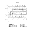
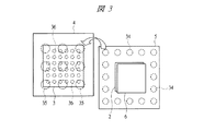
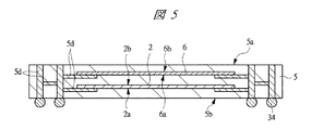
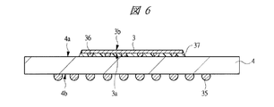
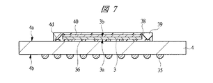
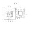
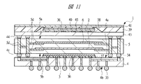
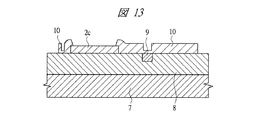
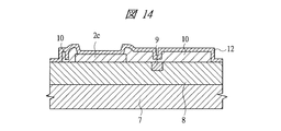
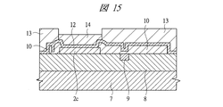
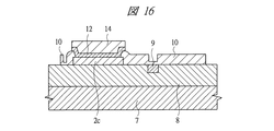
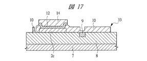
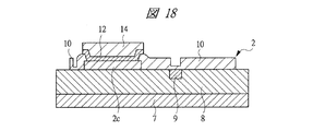
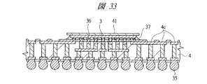
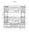
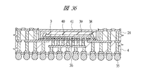
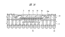
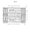
図1は本発明の実施の形態1の半導体装置の構造の一例を模式的に示す断面図、図2は図1に示す半導体装置の等長配線構造を模式的に示す部分構造図、図3は図1に示す半導体装置を基板ごとに展開して構造を示す平面図、図4は本発明の実施の形態1の変形例の半導体装置の構造を模式的に示す断面図である。また、図5は図1に示す半導体装置の上段側パッケージの構造を示す断面図、図6は図1に示す半導体装置の下段側パッケージの構造を示す断面図、図7は図4に示す半導体装置の下段側パッケージの構造を示す断面図、図8は本発明の実施の形態1の変形例の半導体装置の構造を模式的に示す断面図、図9は本発明の実施の形態1の変形例の半導体装置の構造を模式的に示す断面図である。さらに、図10は図8に示す半導体装置を基板ごとに展開して構造を示す平面図、図11は本発明の実施の形態1の変形例の半導体装置の構造を模式的に示す断面図、図12は本発明の実施の形態1の変形例の半導体装置の構造を模式的に示す断面図である。
図1〜図3に示す本実施の形態1の半導体装置は、複数の半導体チップを有するものであり、複数の半導体チップが内蔵された基板を有する半導体パッケージである。本実施の形態1では、前記半導体装置の一例として、SIP1を取り上げて説明する。
SIP1の構成について説明すると、主面(第1主面)4aと主面4aに対向する裏面(第1裏面)4bを有する第1配線基板4と、第1配線基板4の主面4a上に搭載されたマイコンチップ3と、主面(第2主面)5aと主面5aに対向する裏面(第2裏面)5bを有し、かつマイコンチップ3上に配置された第2配線基板5と、第1配線基板4と第2配線基板5とを電気的に接続する複数の第1はんだバンプ(第1バンプ電極)34とから成る。さらに、第1配線基板4の裏面4bには、SIP1の外部端子として複数の第2はんだバンプ(第2バンプ電極)35が格子状に配置されている。
すなわち、SIP1は、第1配線基板4と、第1配線基板4上に搭載されたマイコンチップ3と、マイコンチップ3上に配置された第2配線基板5と、第1配線基板4と第2配線基板5を接続する複数の第1はんだバンプ34と、第1配線基板4の裏面4bに設けられた複数の第2はんだバンプ35とを有し、第1配線基板4を有するパッケージ完結構造上に第2配線基板5を有するパッケージ完結構造が搭載された、所謂POP(Package on Package)構造である。
さらに、第2配線基板5の内部には高速の第1メモリチップ2と第2メモリチップ6が積層した状態で内蔵されており、第2配線基板5内で第1メモリチップ2の配線と第2メモリチップ6の配線が等長化されている。
SIP1の構造について詳細に説明すると、第1配線基板4上に複数の第1はんだバンプ34を介して第2配線基板5が搭載されており、かつ第1配線基板4の主面4aと第2配線基板5の裏面5bとの間の領域に、演算処理機能を備えたマイコンチップ3が配置されている。図3に示すようにマイコンチップ3は、第1配線基板4上でその略中央に配置され、第1配線基板4の主面4aに形成された複数の第1ボンディングリード4cのうちマイコンチップ3用の複数のボンディングリード(図示しない)と、例えば複数の金バンプ36を介してフリップチップ接続されている。すなわち、マイコンチップ3は、図1に示すように、その主面3aを下方に向け、裏面3bを上方に向けて搭載されている。さらに、そのフリップチップ接続部にアンダーフィル37が充填され、このアンダーフィル37によって保護されている。ここで、マイコンチップ3をAuバンプ36を介してフリップチップ接続することで、狭ピッチ化に対応することが可能である。
また、第1配線基板4と第2配線基板5を接続する第1はんだバンプ34は、図3に示すようにマイコンチップ3の外側周囲に配置されている。その際、図1に示すSIP1では、第1配線基板4と第2配線基板5の平面方向の大きさが同じであるため、複数の第1はんだバンプ34は、図3に示すように第1配線基板4及び第2配線基板5の周縁部に並んで配置されている。更に説明すると、複数の第1はんだバンプ34は、第1配線基板4の主面4a上に搭載されたマイコンチップ3の周囲に並んで配置されている。
また、第2配線基板5は、それぞれにメモリ回路を備えた第1メモリチップ2と第2メモリチップ6を内蔵しており、その際、図1に示すように第2メモリチップ6は、第1メモリチップ2上に配置されている。すなわち、第1メモリチップ2及び第2メモリチップ6は、第2配線基板5内に埋め込まれており、その際、第1メモリチップ2上に第2メモリチップ6が積層されている。なお、第1メモリチップ2及び第2メモリチップ6とも、主面2a,6a及び裏面2b,6bがそれぞれ同じ方向を向いて積層されている。
このように本実施の形態1のSIP1では、下段側として、図6に示すように第1配線基板4上にマイコンチップ3が搭載されたパッケージ完結構造となっており、さらに、上段側として、図5に示すように第2配線基板5内に第1メモリチップ2と第2メモリチップ6が内蔵されたパッケージ完結構造となっており、両方のパッケージ完結構造を積層した構造(以降、オンパック構造ともいう)となっている。
したがって、メモリチップ関係のテストと、マイコンチップ関係のテストをそれぞれ独立したパッケージ完結構造にて実施できるため、良品同士を組み合わせて積層することでSIP1の組み立てにおける歩留りを向上させることができる。
また、メモリチップ関係のパッケージ構造と、マイコンチップ関係のパッケージ構造とを自由自在に組み合わせることが可能なため、バリエーションを多数組むことができ、種々の構造を実現できる。その際、テスト後に、組み合わせをユーザ側で選択することも可能になる。
なお、SIP1の上段側に配置された第2配線基板5に内蔵されている第1メモリチップ2及び第2メモリチップ6は、例えば、ダブル・データ・レート・シンクロナスDRAM(Double Data Rate SDRAM) である。ダブル・データ・レート・シンクロナスDRAMは、SDRAMの同期タイミングを強化し、転送レートが2倍となるようにした高速対応のSDRAMであり、外部クロック信号の立ち上がりと立ち下がりの両方に同期してデータを転送するものである。
したがって、第1メモリチップ2と第2メモリチップ6において、外部クロック信号の立ち上がりと立ち下がりの両方を使用するため、極めて短いタイミングを合わせる必要があり、本実施の形態1では、第2配線基板5の内部において、第1メモリチップ2と接続する内部配線5dと、第2メモリチップ6と接続する内部配線5dとの等長化が図られている。
すなわち、図2に示すように、第2配線基板5の内部配線5dにおいて、第1メモリチップ2の第1電極パッド2cからこの第1電極パッド2cに対応する第2配線基板5の第2ボンディングリード5cまでの第1距離5eと、第2メモリチップ6の第2電極パッド6cからこの第2電極パッド6cに対応する第2ボンディングリード5cまでの第2距離5fとが略等しい長さになっている。
これにより、第1メモリチップ2及び第2メモリチップ6において、内部配線5dの等長化が図られているため、外部クロック信号の立ち上がりと立ち下がりの両方に同期してデータを転送することができる。
なお、内部配線5dの等長化に関して、第1距離5eと第2距離5fの差の許容範囲は、例えば、±2mm以内、好ましくは±1mm以内である。
ここで、SIP1では、マイコンチップ3は、システムの外部と、システムの内部に設けられた第1メモリチップ2や第2メモリチップ6との間を仲介してデータの入出力を制御している。すなわち、アドレス、コマンド、クロック等の情報を複数のメモリチップとの間でやり取りしている。そのため、図1に示すように、マイコンチップ3と第1メモリチップ2及び第2メモリチップ6のそれぞれは、複数の第1ボンディングリード4c、複数の第1はんだバンプ34、及び複数の第2ボンディングリード5cを介して電気的に接続されている。このとき、マイコンチップ3の複数の金バンプ36が電気的に接続されるマイコンチップ用のボンディングリードと、複数の第1はんだバンプ34と電気的に接続される複数の第1ボンディングリード4cは、それぞれ電気的に接続されている。
本実施の形態1のSIP1では、マイコンチップ3を下段側、メモリチップを上段側に配置している。
なぜなら、第2配線基板5では、2つの薄い第1メモリチップ2と第2メモリチップ6が内蔵されるため、内部に半導体チップを搭載していない第1配線基板4よりも反り易い。つまり、基板とチップの熱膨張係数の差から第2配線基板5は第1配線基板4に比べて反り易いので、第2配線基板5を下段側に配置した場合、第2配線基板5の表面(主面5a)の平坦性が確保できず、上段側に積層しようとする第1配線基板4の実装不良が発生し易い。しかしながら、SIP1の組み立ての際の第1配線基板4と第2配線基板5のはんだ接続において、予め、第1配線基板4の第1ボンディングリード4c上にはんだペースト46(迎えはんだ)を塗布しておき(図35参照)、このはんだペースト46と第1はんだバンプ34を接続することで、第2配線基板5が反っている場合であっても第1配線基板4と第2配線基板5を接続をすることができる。従って、反りの少ない第1配線基板4を下側に配置するため、ユーザ側でのSIP1の実装も可能になる。
また、マイコンチップ3は、メモリチップに比較して遥かにピン数が多く、かつ発熱量も多い。すなわち、マイコンチップ3は、信号の送受信の外部との仲介役であるとともに、ピン数が多くかつ発熱量も多い。しかしながら、下段の第1配線基板4上に搭載することで、SIP1が実装される実装基板に第2はんだバンプ35を介して熱を逃がすことができる。
以上のように本実施の形態1のSIP1は、第2配線基板5に第1メモリチップ2及び第2メモリチップ6が内蔵され、かつ第2メモリチップ6が第1メモリチップ2上に配置されているとともに、第1メモリチップ2及び第2メモリチップ6は、外部クロック信号の立ち上がりと立ち下がりの両方に同期してデータを転送する高速のメモリチップである。このような複数の高速のメモリチップが内蔵された第2配線基板5において、これらのメモリチップ(第1メモリチップ2及び第2メモリチップ6)の配線の等長化を図ることができる。
さらに、反り易いチップ内蔵の第2配線基板5が上段側に配置されているため、マイコンチップ3から発せられる熱を外部端子である第2はんだバンプ35を介して実装基板に逃がすことができる。
次に、本実施の形態1の変形例について説明する。図4に示す変形例のSIP1は、下段側の第1配線基板4上に半導体チップを積層して実装するものである。第1配線基板4上に積層されている下段の半導体チップは、フリップチップ接続されたマイコンチップ3である。したがって、このマイコンチップ3は、第1配線基板4の第1内部配線4eを介して第1はんだバンプ34や第2はんだバンプ35と電気的に接続されている。
また、図4に示すSIP1の第1配線基板4上に積層されている上段の半導体チップは、マイコンチップ3であってもメモリチップ40であってもどちらでもよく、ワイヤ38を介して第1配線基板4の主面4a上の端子4dと電気的に接続されている。第2配線基板5に内蔵されている第1メモリチップ2や第2メモリチップ6ほど高速処理を必要としないため、第1内部配線4eとは分離された第2内部配線4fを介して端子4dが第2はんだバンプ35と接続されている。なお、下段のマイコンチップ3と上段のメモリチップ40、及びワイヤ38は、封止体39によって樹脂封止されている。
また、図4に示すSIP1においても、下段側として、図7に示すように第1配線基板4上にマイコンチップ3とメモリチップ40が積層されたパッケージ完結構造となっており、さらに、上段側として、図5に示すように第2配線基板5内に第1メモリチップ2と第2メモリチップ6が内蔵されたパッケージ完結構造となっており、両方のパッケージ完結構造を積層した構造(オンパック構造)となっている。
したがって、メモリチップ関係のテストと、マイコンチップ関係のテストをそれぞれ独立したパッケージにて実施できるため、良品同士を組み合わせて積層することで図4に示すSIP1の組み立てにおける歩留りを向上させることができる。
次に、図8に示す変形例のSIP1は、図10に示すように上下段の基板のサイズが異なっているものであり、下段に配置される第1配線基板4の方が上段に配置される第2配線基板5より遥かに大きなものとなっている。さらに、図8に示すように、第2配線基板5と、第1配線基板4の第2配線基板5から迫り出した箇所が放熱板41によって覆われており、SIP1の放熱性を向上させることができる。放熱板41は、第1配線基板4の主面4aの周縁部に接着剤42を介して固着されている。
また、図9に示す変形例のSIP1は、第1配線基板4の第2配線基板5から迫り出した箇所のみに接着剤42を介して放熱板41が固着されているものであり、これによってもSIP1の放熱性を向上させることができる。
また、図11に示す変形例のSIP1は、第1配線基板4上に第2配線基板5を積層し、さらに第2配線基板5上に第3はんだバンプ44を介して第3配線基板43が積層されているものである。第3配線基板43上には、例えば、その下段にはマイコンチップ45が金バンプ36を介してフリップチップ接続され、さらにその上にメモリチップ40が積層されており、メモリチップ40は、ワイヤ38を介して第3配線基板43に電気的に接続されている。第3配線基板43上のマイコンチップ45及びメモリチップ40やワイヤ38は、封止体39によって樹脂封止され、さらに、封止体39の表面には放熱板41が貼り付けられている。
また、図12に示す変形例のSIP1は、第1メモリチップ2と第2メモリチップ6が埋め込まれた第2配線基板5の主面5a上に、例えば、メモリチップ40(マイコンチップ45でもよい)が搭載されたものであり、このメモリチップ40がワイヤ38を介して第2配線基板5の主面5aの端子5gと電気的に接続されている。メモリチップ40は、第2配線基板5に内蔵されている第1メモリチップ2や第2メモリチップ6ほど高速処理を必要としないため、第2配線基板5の内部配線5dとは分離された他の内部配線5hを介して端子5gが第1はんだバンプ34と接続され、さらに、第1はんだバンプ34が第1配線基板4の第2内部配線4fを介して第2はんだバンプ35と接続されている。
なお、第2配線基板5の主面5a上において、メモリチップ40やワイヤ38は、封止体39によって樹脂封止され、さらに、封止体39の表面には放熱板41が貼り付けられているとともに、第1配線基板4の第2配線基板5から迫り出した周縁部にも放熱板41が貼り付けられている。
このように図11及び図12にそれぞれ示す変形例のSIP1は、多層のオンパック構造のパッケージであり、図1に示すSIP1と同様の効果を得ることができるとともに、より多数の半導体チップ(メモリチップ40やマイコンチップ45等)を搭載していることにより、さらに機能を向上させたSIP1を実現できる。
次に、本実施の形態1の図1に示すSIP1の組み立てについて説明する。
図13〜図18はそれぞれ図1に示す半導体装置の組み立てにおける内蔵チップの形成方法の一例を示す部分断面図、図19〜図21はそれぞれ図1に示す半導体装置の組み立てにおけるチップ埋め込み方法の一例を示す部分断面図、図22〜図25はそれぞれ変形例のチップ埋め込み方法を示す部分断面図である。また、図26は図1に示す半導体装置の組み立てにおけるチップ埋め込み方法の一例を示す部分断面図、図27は図1に示す半導体装置の組み立てにおける内蔵チップの積層方法の一例を示す部分断面図、図28は図1に示す半導体装置の組み立てにおける内蔵チップの積層後の基板の構造の一例を示す裏面図、図29は図28のA−A線に沿って切断した構造の一例を示す断面図である。さらに、図30は図1に示す半導体装置の組み立てにおける第1バンプ電極の取り付け後の構造の一例を示す部分断面図、図31は変形例の第1バンプ電極の取り付け後の構造を示す部分断面図、図32は図1に示す半導体装置の組み立てにおける基板個片化及びテスト完了後の構造の一例を示す断面図、図33は図1に示す半導体装置の組み立てにおける下側パッケージのテスト完了後の構造の一例を示す部分断面図である。
また、図34は図1に示す半導体装置の組み立て完了後の構造の一例を示す部分断面図、図35は図1に示す半導体装置の組み立てにおける迎えはんだ形成時の構造の一例を示す部分断面図、図36〜図38はそれぞれ変形例の下側パッケージのテスト完了後の構造を示す部分断面図、図39は変形例の半導体装置の組み立てにおける第1バンプ電極の取り付け後の構造を示す部分断面図である。
まず、図13に示すように、Siベース7上にデバイス層8が形成され、さらにデバイス層8上に第1電極パッド2cとパッシベーション膜10が形成されたデバイスにおいて、プローブ検査とヒューズ9の切断を行って良品のデバイスを取得する。
その後、図14に示すように、第1電極パッド2c及びパッシベーション膜10上に電極層であるシード層12を形成する。
その後、図15に示すように、シード層12上にレジスト膜13を形成し、その後、第1電極パッド2c上のレジスト膜13を所定形状で除去した後、第1電極パッド2c上のシード層12上にCu電極14を形成する。
その後、図16に示すように、Cu電極14の周囲のレジスト膜13及びシード層12を除去し、第1電極パッド2c上のCu電極14を完成させる。なお、Cu電極14の形成についてはスパッタ法等の他の方法で形成してもよい。
その後、図17に示すように、Siベース裏面を研磨して薄膜化デバイス33を形成する。
その後、ダイシングによる個片化を行って図18に示す第1メモリチップ2を取得する。
その後、図19に示すように、多連の第1ベース基板15を準備し、さらに、第1ベース基板15上に樹脂層17と、凹部であるキャビティ16を形成する。
その後、図18で形成した第1メモリチップ2を第1ベース基板15上に形成したキャビティ16内に配置し、ダイボンド材18で固着する。
その後、キャビティ16内において、図20に示すように第1メモリチップ2上にエポキシ樹脂等からなる絶縁材19を充填し、さらに、第1メモリチップ2の第1電極パッド2c上のCu電極14の上部を開口する。
その後、レーザ加工等によって樹脂層17の所定箇所に貫通孔を形成し、続いて図21に示すように、めっきによって貫通孔の内壁にスルーホール配線23を形成するとともに、その内部に充填材22を埋め込み、さらにCu電極14に接続する配線パターンである導体パターン20、及び導体パターン20とスルーホール配線23を接続するビアパッド24を形成する。その際、ビアパッド24を導体パターン20によって覆う。
なお、図22及び図23の変形例に示すように、第1ベース基板15上にチップマウント後、チップ周囲をプリプレグ等の絶縁材19で覆う構造としてもよく、絶縁材19で覆った後に、第1電極パッド2c上のCu電極14の上部を開口すればよい。開口後、ビアパッド24と、このビアパッド24を覆い、かつCu電極14と接続する導体パターン20を形成する。
また、図19に示すキャビティ構造を利用して、図24及び図25の変形例に示すように、樹脂層17の上部にエポキシ樹脂等からなる絶縁材19を配置しない構造としてもよい。すなわち、キャビティ16内のみに絶縁材19を充填するものである。
その後、図26に示すように、導体パターン20上にプリプレグ等からなる絶縁層11を形成するとともに、ビアパッド24上にパッド26を形成する。
その後、図27に示すように、第2ベース基板21を準備する。ここで、第2ベース基板21は、樹脂層17(第1ベース基板15を含む)とほぼ同じ厚さであり、第2ベース基板21の所定箇所にスルーホール配線23と、このスルーホール配線23に接続されるビアパッド24及び中継パターン25を形成する。
その後、図28及び図29に示すように、第2ベース基板21の表面側に、第2メモリチップ6が埋め込まれた樹脂層17(第1ベース基板15を含む)を配置し、さらに、第2ベース基板21の裏面側に、第1メモリチップ2が埋め込まれた樹脂層17(第1ベース基板15を含む)を配置し、加熱プレス等によって第2ベース基板21と表裏両面の樹脂層17とをそれぞれ接着する。その際、第2ベース基板21の表裏両面の第2メモリチップ6と第1メモリチップ2が同じ方向を向くようにそれぞれの樹脂層17と第2ベース基板21とを接着する。
その結果、第2ベース基板21を間に介在させた状態で第2メモリチップ6と第1メモリチップ2が積層されるとともに、上下のメモリチップの等長配線を行うことができる。ここでは、図29に示すように、第2メモリチップ6と第1メモリチップ2にそれぞれ接続されている導体パターン20は、それぞれスルーホール配線23を介してA部で中継パターン25に接続しており、これによって配線の等長化が図られている(図29における黒塗り配線が等長化配線となっている)。
その後、基板の表裏両面にレジスト膜27を形成する。
これによって、第1メモリチップ2と第2メモリチップ6が積層されて埋め込まれ、かつ等長化配線が形成されたパッケージ完結構造の形成を完了する。
その後、図30に示すように、パッケージ完結構造(第2配線基板5)の裏面5bのパッド26(第2ボンディングリード5c)に、第1はんだバンプ34を接続する。
なお、図31に示す変形例は、パッケージ完結構造(第2配線基板5)のパッド26(第2ボンディングリード5c)に第1はんだバンプ34を接続する際に、第1配線基板4上に第2配線基板5を接続した時に、第1メモリチップ2及び第2メモリチップ6のデバイス面が上方を向くようにするものである。すなわち、パッケージ完結構造(第2配線基板5)の主面5aのパッド26(第2ボンディングリード5c)に第1はんだバンプ34を接続するものである。これにより、基板が反っていてもその実装性を向上できるとともに、基板の放熱性を向上させることができる。
その後、図32に示すように、ダイシングによって基板の個片化を行って第2配線基板5を形成し、さらにこのパッケージ完結構造(メモリスタックパッケージ)のメモリテストを行う。
その後、図33に示すように、マイコンチップ3がフリップチップ接続で搭載され、かつ第2はんだバンプ35が接続され、さらにテストが完了した第1配線基板4(パッケージ完結構造)を準備する。
その後、図34に示すように、第1はんだバンプ34を介して上段の第2配線基板5を有するパッケージ完結構造と、下段の第1配線基板4を有するパッケージ完結構造とを接続することでSIP1の組み立てを完了する。
なお、第1配線基板4と第2配線基板5を接続する際には、熱及び荷重を掛けた状態で第2配線基板5を第1配線基板4上に実装する。さらに、図35に示すように、予め第1配線基板4の第1ボンディングリード4c上に迎えはんだを塗布しておき、前記迎えはんだと第2配線基板5に接続されている第1はんだバンプ34とを接続することが好ましい。すなわち、第1配線基板4の主面4aの複数の第1ボンディングリード4c上に予め迎えはんだであるはんだペースト46を塗布しておき、熱及び荷重を掛けて第1はんだバンプ34とはんだペースト46とを接続して第1配線基板4上に第2配線基板5を実装することが好ましい。
これは、上段に配置される第2配線基板5には、薄い第1メモリチップ2と第2メモリチップ6が積層して埋め込まれているため、基板が反り易い。したがって、上段に配置される第2配線基板5と下段に配置される第1配線基板4とを接続する際には、下段側の第1配線基板4の第1ボンディングリード4c上に予めはんだペースト46(迎えはんだ)を塗布しておき、熱及び荷重を掛けて第2配線基板5を実装することで、上段側の第2配線基板5の反りを吸収してはんだ接続を行うことができるためである。熱及び荷重から解放されると、第2配線基板5は再び反るが、その時には、すでに第1配線基板4と第2配線基板5は、はんだが硬化して接続を完了しているため、接続不良に至ることは無い。
したがって、第1配線基板4にはんだペースト46を塗布せずに、単に、熱及び荷重を掛けるだけでも良いが、より好ましくは迎えはんだであるはんだペースト46を予め第1配線基板4に塗布しておくことで、反り易いチップ内蔵の第2配線基板5をより確実に実装することができる。
すなわち、迎えはんだ技術を採用することで、複数のチップ内蔵の反り易い第2配線基板5を上段に配置してはんだ実装することが可能になる。その結果、マイコンチップ3が搭載された反りにくい第1配線基板4は下段に配置し、かつ反り易い第2配線基板5を第1はんだバンプ34を介して第1配線基板4上に実装することが可能になるため、ユーザ側で第2配線基板5の実装を行うことも可能になる。
次に、図36は変形例を示すものであり、第1配線基板4上に、例えば、マイコンチップ3とメモリチップ40を積層して実装した結果、これらチップを樹脂封止する封止体39の高さがより高くなってしまう場合がある。そのため、この封止体39の周囲に第1はんだバンプ34を介して別のパッケージを積層するPOP(Package On Package)構造を採用できない。そこで、第1配線基板4上の第1ボンディングリード4cを封止体39の上面よりも高い位置に引出すために、スペーサ基板28を介在させてテストを行うものである。テスト終了後は、スペーサ基板28を離脱させて、図37に示すように、元の第1配線基板4の構造にもどすことが可能である。
また、図38に示す変形例は、第1配線基板4上に積層されたマイコンチップ3とメモリチップ40において、上段のメモリチップ40と基板とをワイヤ38を介して接続する際に、スペーサ基板28のキャビティ内側に段差部28aを設けておき、この段差部28aの電極にワイヤ38を接続してテストを行うものである。段差部28aを設けておけば、フリップチップ接続されたマイコンチップ3と第1配線基板4との間にアンダーフィル樹脂を充填しても、メモリチップ40とワイヤ38を介して電気的に接続される第1配線基板4上のボンディングリードがアンダーフィル樹脂で覆われ難くなる。
また、図39に示す変形例は、第2配線基板5において第1メモリチップ2と第2メモリチップ6を積層した状態で埋め込む際に、両チップを逆向きで積層するものである。すなわち、第1メモリチップ2の裏面2bと第2メモリチップ6の裏面6bとが向かい合って積層されており、この構造においても、両チップをそれぞれスルーホール配線23を介して中継パターン25に接続することにより、配線の等長化を図ることができる。
(実施の形態2)
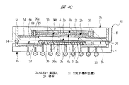
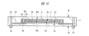
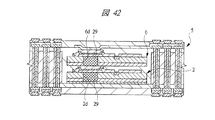
図40は本発明の実施の形態2の半導体装置の構造の一例を模式的に示す断面図、図41は図40に示す半導体装置の上段側パッケージの構造を示す断面図、図42は図41に示す上段側パッケージの基板の内部構造の一例を示す部分断面図である。
図40に示す本実施の形態2のSIP31は、第2配線基板5に内蔵される半導体チップそれぞれが、貫通孔2d,6d,30cを有するものであり、それぞれの貫通孔2d,6d,30c内に導体29が埋め込まれて配線が等長化されているものである。
したがって、図41に示すように、第2配線基板5に第1メモリチップ2と第2メモリチップ6と第3メモリチップ30が積層して埋め込まれており、この構造でパッケージ完結構造としてメモリテストを行うことが可能である。なお、各チップは、それぞれの主面2a,6a,30a及び裏面2b,6b,30bが同一の方向を向いて積層されており、貫通孔2d,6d,30cに埋め込まれた導体29を介して電気的に接続されている。
なお、図42は、第1メモリチップ2と第2メモリチップ6のみが積層されて埋め込まれた第2配線基板5を有するパッケージ完結構造の詳細を示しており、このパッケージ完結構造においてもチップ厚が薄いため、導体29を介して配線の等長化を図ることができる。その結果、実施の形態1のSIP1と同様の効果を得ることができる。
(実施の形態3)
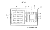
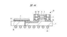
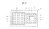
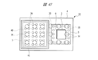
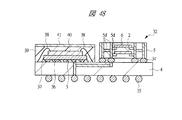
図43は本発明の実施の形態3の半導体装置の構造の一例を模式的に透過して示す平面図、図44は図43に示す半導体装置の断面図、図45乃至図48はそれぞれ本発明の実施の形態3の変形例の半導体装置の構造を模式的に透過して示す平面図と断面図である。
本実施の形態3の半導体装置(SIP32)は、第1配線基板4上に第2配線基板5を実装する際に、マイコンチップ3と第2配線基板5を横置き(平置き)に実装するものであり、図43、図45、及び図47に示すSIP32では、それぞれの内部構造を上方から透過して示している。
図43及び図44は、第1配線基板4上に金バンプ36を介してフリップチップ接続されたマイコンチップ3の横に、第1メモリチップ2と第2メモリチップ6が積層して埋め込まれた第2配線基板5を第1はんだバンプ34を介して実装した構造を示している。第1配線基板4の裏面側には複数の第2はんだバンプ35が設けられている。
図45及び図46のSIP32では、第1配線基板4上に金バンプ36を介してフリップチップ接続されたマイコンチップ3が実装され、さらにマイコンチップ3上に、例えば、メモリチップ40等が積層されて実装されている。この場合も、マイコンチップ3の横に、第1メモリチップ2と第2メモリチップ6が積層して埋め込まれた第2配線基板5が第1はんだバンプ34を介して実装されており、さらに、第1配線基板4の裏面側には複数の第2はんだバンプ35が設けられている。
図47及び図48のSIP32は、図45のSIP32のマイコンチップ3上に積層されたメモリチップ40のさらに上部に放熱板41が設けられている場合であり、放熱板41以外の構造は、図45のSIP32と同様である。
図43〜図48に示すSIP32においても、第1配線基板4上に実装されたチップ内蔵の第2配線基板5で複数の半導体チップの配線の等長化を図ることができ、実施の形態1のSIP1と同様の効果を得ることができる。
以上、本発明者によってなされた発明を発明の実施の形態に基づき具体的に説明したが、本発明は前記発明の実施の形態に限定されるものではなく、その要旨を逸脱しない範囲で種々変更可能であることは言うまでもない。
例えば、前記実施の形態1〜3では、上段側の第2配線基板5に2つまたは3つの半導体チップが積層して内蔵されている場合を説明したが、内蔵される半導体チップの積層数は、2つ以上であれば何層であってもよい。
また、例えばマイコンチップ3のフリップチップ接続には、金バンプに限定されるものではなく、半田バンプを使用してもよい。図43〜図48に示すように、マイコンチップ3とメモリチップ(第1メモリチップ2と第2メモリチップ6)を内蔵した第2配線基板5とが平置きに搭載されている場合、それぞれを第1配線基板4上に実装してから、一括してリフロー処理することが可能であり、Auバンプを使用する場合に比べ、実装工程の簡略化が可能である。
本発明は、マイコンチップとメモリチップを有する電子装置に好適である。
本発明の実施の形態1の半導体装置の構造の一例を模式的に示す断面図である。 図1に示す半導体装置の等長配線構造を模式的に示す部分構造図である。 図1に示す半導体装置を基板ごとに展開して構造を示す平面図である。 本発明の実施の形態1の変形例の半導体装置の構造を模式的に示す断面図である。 図1に示す半導体装置の上段側パッケージの構造を示す断面図である。 図1に示す半導体装置の下段側パッケージの構造を示す断面図である。 図4に示す半導体装置の下段側パッケージの構造を示す断面図である。 本発明の実施の形態1の変形例の半導体装置の構造を模式的に示す断面図である。 本発明の実施の形態1の変形例の半導体装置の構造を模式的に示す断面図である。 図8に示す半導体装置を基板ごとに展開して構造を示す平面図である。 本発明の実施の形態1の変形例の半導体装置の構造を模式的に示す断面図である。 本発明の実施の形態1の変形例の半導体装置の構造を模式的に示す断面図である。 図1に示す半導体装置の組み立てにおける内蔵チップの形成方法の一例を示す部分断面図である。 図1に示す半導体装置の組み立てにおける内蔵チップの形成方法の一例を示す部分断面図である。 図1に示す半導体装置の組み立てにおける内蔵チップの形成方法の一例を示す部分断面図である。 図1に示す半導体装置の組み立てにおける内蔵チップの形成方法の一例を示す部分断面図である。 図1に示す半導体装置の組み立てにおける内蔵チップの形成方法の一例を示す部分断面図である。 図1に示す半導体装置の組み立てにおける内蔵チップの形成方法の一例を示す部分断面図である。 図1に示す半導体装置の組み立てにおけるチップ埋め込み方法の一例を示す部分断面図である。 図1に示す半導体装置の組み立てにおけるチップ埋め込み方法の一例を示す部分断面図である。 図1に示す半導体装置の組み立てにおけるチップ埋め込み方法の一例を示す部分断面図である。 変形例のチップ埋め込み方法を示す部分断面図である。 変形例のチップ埋め込み方法を示す部分断面図である。 変形例のチップ埋め込み方法を示す部分断面図である。 変形例のチップ埋め込み方法を示す部分断面図である。 図1に示す半導体装置の組み立てにおけるチップ埋め込み方法の一例を示す部分断面図である。 図1に示す半導体装置の組み立てにおける内蔵チップの積層方法の一例を示す部分断面図である。 図1に示す半導体装置の組み立てにおける内蔵チップの積層後の基板の構造の一例を示す裏面図である。 図28のA−A線に沿って切断した構造の一例を示す断面図である。 図1に示す半導体装置の組み立てにおける第1バンプ電極の取り付け後の構造の一例を示す部分断面図である。 変形例の第1バンプ電極の取り付け後の構造を示す部分断面図である。 図1に示す半導体装置の組み立てにおける基板個片化及びテスト完了後の構造の一例を示す断面図である。 図1に示す半導体装置の組み立てにおける下側パッケージのテスト完了後の構造の一例を示す部分断面図である。 図1に示す半導体装置の組み立て完了後の構造の一例を示す部分断面図である。 図1に示す半導体装置の組み立てにおける迎えはんだ形成時の構造の一例を示す部分断面図である。 変形例の下側パッケージのテスト完了後の構造を示す部分断面図である。 変形例の下側パッケージのテスト完了後の構造を示す部分断面図である。 変形例の下側パッケージのテスト完了後の構造を示す部分断面図である。 変形例の半導体装置の組み立てにおける第1バンプ電極の取り付け後の構造を示す部分断面図である。 本発明の実施の形態2の半導体装置の構造の一例を模式的に示す断面図である。 図40に示す半導体装置の上段側パッケージの構造を示す断面図である。 図41に示す上段側パッケージの基板の内部構造の一例を示す部分断面図である。 本発明の実施の形態3の半導体装置の構造の一例を模式的に透過して示す平面図である。 図43に示す半導体装置の断面図である。 本発明の実施の形態3の変形例の半導体装置の構造を模式的に透過して示す平面図である。 図45に示す半導体装置の断面図である。 本発明の実施の形態3の変形例の半導体装置の構造を模式的に透過して示す平面図である。 図47に示す半導体装置の断面図である。
符号の説明
1 SIP(半導体装置)
2 第1メモリチップ
2a 主面
2b 裏面
2c 第1電極パッド
2d 貫通孔
3 マイコンチップ
3a 主面
3b 裏面
4 第1配線基板
4a 主面
4b 裏面
4c 第1ボンディングリード
4d 端子
4e 第1内部配線
4f 第2内部配線
5 第2配線基板
5a 主面
5b 裏面
5c 第2ボンディングリード
5d 内部配線
5e 第1距離
5f 第2距離
5g 端子
5h 他の内部配線
6 第2メモリチップ
6a 主面
6b 裏面
6c 第2電極パッド
6d 貫通孔
7 Siベース
8 デバイス層
9 ヒューズ
10 パッシベーション膜
11 絶縁層
12 シード層
13 レジスト膜
14 Cu電極
15 第1ベース基板
16 キャビティ
17 樹脂層
18 ダイボンド材
19 絶縁材
20 導体パターン
21 第2ベース基板
22 充填材
23 スルーホール配線
24 ビアパッド
25 中継パターン
26 パッド
27 レジスト膜
28 スペーサ基板
28a 段差部
29 導体
30 第3メモリチップ
30a 主面
30b 裏面
30c 貫通孔
31,32 SIP(半導体装置)
33 薄膜化デバイス
34 第1はんだバンプ(第1バンプ電極)
35 第2はんだバンプ(第2バンプ電極)
36 金バンプ
37 アンダーフィル
38 ワイヤ
39 封止体
40 メモリチップ
41 放熱板
42 接着剤
43 第3配線基板
44 第3はんだバンプ
45 マイコンチップ
46 はんだペースト

Claims (6)

  1. 第1主面、前記第1主面に形成された第1ボンディングリード、及び前記第1主面とは反対側の第1裏面を有する第1配線基板と、
    演算処理機能を有し、前記第1配線基板の前記第1主面に搭載されたマイコンチップと、
    第2主面、前記第2主面に形成された端子、前記第2主面とは反対側の第2裏面、及び前記第2裏面に形成された第2ボンディングリードを有し、前記マイコンチップが搭載された前記第1配線基板上に配置された第2配線基板と、
    前記第1配線基板の前記第1ボンディングリードと前記第2配線基板の前記第2ボンディングリードとを電気的に接続する第1バンプ電極と、
    前記第1配線基板の前記第1裏面に配置された第2バンプ電極と、
    前記第2配線基板の前記第2主面と前記第2配線基板の前記第2裏面との間に配置された第1メモリチップと、
    前記第2配線基板の前記第2主面と前記第2配線基板の前記第2裏面との間において、前記第1メモリチップ上に配置された第2メモリチップと、を含み、
    前記マイコンチップは、前記第1配線基板に形成された第1内部配線を介して前記第1ボンディングリードと電気的に接続され、
    前記マイコンチップは、前記第1配線基板に形成された第2内部配線を介して前記第2バンプ電極と電気的に接続され、
    前記第1メモリチップは、前記第2配線基板に形成された第3内部配線を介して前記第2ボンディングリードと電気的に接続され、
    前記第2メモリチップは、前記第2配線基板に形成された第4内部配線を介して前記第2ボンディングリードと電気的に接続されており、
    前記マイコンチップは、前記第1及び第2メモリチップと外部機器とのインタフェースであり、
    前記第1及び第2メモリチップのそれぞれは、外部クロック信号の立ち上がりと立ち下がりの両方に同期してデータを転送するダブル・データ・レート・シンクロナスDRAMであることを特徴とする半導体装置。
  2. 請求項記載の半導体装置において、前記マイコンチップと前記第1及び第2メモリチップのそれぞれは、前記第1ボンディングリード、前記第1バンプ電極、及び前記第2ボンディングリードを介して電気的に接続されていることを特徴とする半導体装置。
  3. 請求項記載の半導体装置において、前記第1メモリチップの第1電極パッドから前記第2ボンディングリードまでの第1距離と、前記第2メモリチップの第2電極パッドから前記第2ボンディングリードまでの第2距離は等しいことを特徴とする半導体装置。
  4. 請求項記載の半導体装置において、前記第1距離と前記第2距離の差の許容範囲は、±1mm以内であることを特徴とする半導体装置。
  5. 請求項1記載の半導体装置において、前記端子は、前記第2配線基板の内部に形成された第5内部配線を介して、前記第1配線基板と前記第2配線基板との間に設けられた第3バンプ電極と電気的に接続されていることを特徴とする半導体装置。
  6. 請求項5記載の半導体装置において、前記端子は、前記第5内部配線、前記第3バンプ電極、及び前記第1配線基板の内部に形成された第6内部配線を介して、前記第1配線基板の前記第1裏面に形成された第4バンプ電極と電気的に接続されていることを特徴とする半導体装置。
JP2006183993A 2006-07-04 2006-07-04 半導体装置 Expired - Fee Related JP5259059B2 (ja)

Priority Applications (5)

Application Number Priority Date Filing Date Title
JP2006183993A JP5259059B2 (ja) 2006-07-04 2006-07-04 半導体装置
US11/798,737 US7847413B2 (en) 2006-07-04 2007-05-16 Semiconductor device and method of manufacturing the same
TW096118100A TW200816435A (en) 2006-07-04 2007-05-22 Semiconductor device and method of manufacturing the same
CNA2007101101300A CN101101909A (zh) 2006-07-04 2007-06-18 半导体器件及其制造方法
KR1020070065074A KR20080004356A (ko) 2006-07-04 2007-06-29 반도체 장치 및 그 제조 방법

Applications Claiming Priority (1)

Application Number Priority Date Filing Date Title
JP2006183993A JP5259059B2 (ja) 2006-07-04 2006-07-04 半導体装置

Publications (3)

Publication Number Publication Date
JP2008016519A JP2008016519A (ja) 2008-01-24
JP2008016519A5 JP2008016519A5 (ja) 2009-08-20
JP5259059B2 true JP5259059B2 (ja) 2013-08-07

Family

ID=38918408

Family Applications (1)

Application Number Title Priority Date Filing Date
JP2006183993A Expired - Fee Related JP5259059B2 (ja) 2006-07-04 2006-07-04 半導体装置

Country Status (5)

Country Link
US (1) US7847413B2 (ja)
JP (1) JP5259059B2 (ja)
KR (1) KR20080004356A (ja)
CN (1) CN101101909A (ja)
TW (1) TW200816435A (ja)

Families Citing this family (32)

* Cited by examiner, † Cited by third party
Publication number Priority date Publication date Assignee Title
JP4185499B2 (ja) * 2005-02-18 2008-11-26 富士通マイクロエレクトロニクス株式会社 半導体装置
SG147400A1 (en) * 2007-04-24 2008-11-28 United Test & Assembly Ct Ltd Bump on via-packaging and methodologies
US7759212B2 (en) * 2007-12-26 2010-07-20 Stats Chippac, Ltd. System-in-package having integrated passive devices and method therefor
US8258015B2 (en) * 2008-02-22 2012-09-04 Stats Chippac Ltd. Integrated circuit package system with penetrable film adhesive
US8304869B2 (en) * 2008-08-01 2012-11-06 Stats Chippac Ltd. Fan-in interposer on lead frame for an integrated circuit package on package system
JP5140565B2 (ja) * 2008-11-28 2013-02-06 三洋電機株式会社 素子搭載用基板、半導体モジュール、および携帯機器
US8097956B2 (en) * 2009-03-12 2012-01-17 Apple Inc. Flexible packaging for chip-on-chip and package-on-package technologies
JP2010238995A (ja) * 2009-03-31 2010-10-21 Sanyo Electric Co Ltd 半導体モジュールおよびこれを搭載したカメラモジュール
JP5521424B2 (ja) * 2009-07-28 2014-06-11 セイコーエプソン株式会社 集積回路装置、電子機器及び電子機器の製造方法
US8064202B2 (en) * 2010-02-24 2011-11-22 Monolithic Power Systems, Inc. Sandwich structure with double-sided cooling and EMI shielding
KR101686199B1 (ko) 2010-03-26 2016-12-14 삼성전자주식회사 반도체 패키지 구조물
KR101817159B1 (ko) 2011-02-17 2018-02-22 삼성전자 주식회사 Tsv를 가지는 인터포저를 포함하는 반도체 패키지 및 그 제조 방법
CN102157394A (zh) * 2011-03-22 2011-08-17 南通富士通微电子股份有限公司 高密度系统级封装方法
US8674516B2 (en) * 2011-06-22 2014-03-18 Stats Chippac Ltd. Integrated circuit packaging system with vertical interconnects and method of manufacture thereof
KR20130007049A (ko) * 2011-06-28 2013-01-18 삼성전자주식회사 쓰루 실리콘 비아를 이용한 패키지 온 패키지
US8816404B2 (en) 2011-09-16 2014-08-26 Stats Chippac, Ltd. Semiconductor device and method of forming stacked semiconductor die and conductive interconnect structure through an encapsulant
KR101797079B1 (ko) * 2011-12-30 2017-11-14 삼성전자 주식회사 Pop 구조의 반도체 패키지
US8742597B2 (en) 2012-06-29 2014-06-03 Intel Corporation Package substrates with multiple dice
CN103579128B (zh) * 2012-07-26 2016-12-21 碁鼎科技秦皇岛有限公司 芯片封装基板、芯片封装结构及其制作方法
US9368477B2 (en) * 2012-08-27 2016-06-14 Invensas Corporation Co-support circuit panel and microelectronic packages
US8860202B2 (en) * 2012-08-29 2014-10-14 Macronix International Co., Ltd. Chip stack structure and manufacturing method thereof
JP5996500B2 (ja) * 2013-09-11 2016-09-21 株式会社東芝 半導体装置および記憶装置
US9281284B2 (en) * 2014-06-20 2016-03-08 Freescale Semiconductor Inc. System-in-packages having vertically-interconnected leaded components and methods for the fabrication thereof
JP6543129B2 (ja) 2015-07-29 2019-07-10 ルネサスエレクトロニクス株式会社 電子装置
KR102438753B1 (ko) * 2015-10-01 2022-09-01 에스케이하이닉스 주식회사 반도체 장치
WO2017122449A1 (ja) * 2016-01-15 2017-07-20 ソニー株式会社 半導体装置および撮像装置
US11487445B2 (en) * 2016-11-22 2022-11-01 Intel Corporation Programmable integrated circuit with stacked memory die for storing configuration data
CN108400117A (zh) * 2017-02-06 2018-08-14 钰桥半导体股份有限公司 三维整合的散热增益型半导体组件及其制作方法
US10475770B2 (en) 2017-02-28 2019-11-12 Amkor Technology, Inc. Semiconductor device having stacked dies and stacked pillars and method of manufacturing thereof
JP6679528B2 (ja) * 2017-03-22 2020-04-15 キオクシア株式会社 半導体装置
TWI678747B (zh) * 2018-10-01 2019-12-01 點序科技股份有限公司 測試裝置及其晶片承載板
JP2020150145A (ja) * 2019-03-14 2020-09-17 キオクシア株式会社 半導体装置

Family Cites Families (13)

* Cited by examiner, † Cited by third party
Publication number Priority date Publication date Assignee Title
JP2001068617A (ja) * 1999-08-27 2001-03-16 Toshiba Corp 半導体装置
JP3853219B2 (ja) * 2002-01-18 2006-12-06 イビデン株式会社 半導体素子内蔵基板および多層回路基板
JP4069771B2 (ja) * 2003-03-17 2008-04-02 セイコーエプソン株式会社 半導体装置、電子機器および半導体装置の製造方法
JP2004281920A (ja) * 2003-03-18 2004-10-07 Seiko Epson Corp 半導体装置、電子デバイス、電子機器、半導体装置の製造方法および電子デバイスの製造方法
JP4419049B2 (ja) * 2003-04-21 2010-02-24 エルピーダメモリ株式会社 メモリモジュール及びメモリシステム
JP4174013B2 (ja) * 2003-07-18 2008-10-29 株式会社ルネサステクノロジ 半導体装置
JP3858854B2 (ja) 2003-06-24 2006-12-20 富士通株式会社 積層型半導体装置
JP2006032379A (ja) * 2004-07-12 2006-02-02 Akita Denshi Systems:Kk 積層半導体装置及びその製造方法
JP4199724B2 (ja) * 2004-12-03 2008-12-17 エルピーダメモリ株式会社 積層型半導体パッケージ
JP4408090B2 (ja) * 2005-03-01 2010-02-03 パナソニック株式会社 部品内蔵モジュールの製造方法
TWI267967B (en) * 2005-07-14 2006-12-01 Chipmos Technologies Inc Chip package without a core and stacked chip package structure using the same
US7550680B2 (en) * 2006-06-14 2009-06-23 Stats Chippac Ltd. Package-on-package system
US7667338B2 (en) * 2006-08-08 2010-02-23 Lin Paul T Package with solder-filled via holes in molding layers

Also Published As

Publication number Publication date
JP2008016519A (ja) 2008-01-24
US20080006947A1 (en) 2008-01-10
TW200816435A (en) 2008-04-01
US7847413B2 (en) 2010-12-07
KR20080004356A (ko) 2008-01-09
CN101101909A (zh) 2008-01-09

Similar Documents

Publication Publication Date Title
JP5259059B2 (ja) 半導体装置
JP3685947B2 (ja) 半導体装置及びその製造方法
JP5016811B2 (ja) 半導体装置
US20120208322A1 (en) Semiconductor device and manufacturing method therefor
JP2013162128A (ja) パッケージ−オン−パッケージタイプの半導体パッケージ及びその製造方法
KR20090039411A (ko) 솔더 볼과 칩 패드가 접합된 구조를 갖는 반도체 패키지,모듈, 시스템 및 그 제조방법
JP2006049569A (ja) スタック型半導体装置パッケージおよびその製造方法
KR20090025593A (ko) 반도체 패키지가 삽입된 인쇄회로기판
JP2008218979A (ja) 電子パッケージ及びその製造方法
JP2008258522A (ja) 半導体装置の製造方法
JP4033968B2 (ja) 複数チップ混載型半導体装置
WO2004112129A1 (ja) 電子装置
JPWO2003012863A1 (ja) 半導体装置及びその製造方法
JP2009065066A (ja) 半導体装置
JP2008010705A (ja) チップ埋め込み基板のパッケージ構造
TWI435667B (zh) 印刷電路板組件
KR101089647B1 (ko) 단층 패키지 기판 및 그 제조방법
JP4339032B2 (ja) 半導体装置
JP2003249606A (ja) 半導体装置及びインターポーザー
JP2010098225A (ja) 半導体装置
JP2008172123A (ja) 半導体装置
KR20080062565A (ko) 플립 칩 패키지
JP2009246313A (ja) 半導体装置及びその製造方法
CN113707651A (zh) 半导体封装结构和半导体封装结构的制备方法
JP2001291818A (ja) 半導体装置およびその製造方法

Legal Events

Date Code Title Description
A521 Request for written amendment filed

Free format text: JAPANESE INTERMEDIATE CODE: A523

Effective date: 20090701

A621 Written request for application examination

Free format text: JAPANESE INTERMEDIATE CODE: A621

Effective date: 20090701

A977 Report on retrieval

Free format text: JAPANESE INTERMEDIATE CODE: A971007

Effective date: 20091127

A711 Notification of change in applicant

Free format text: JAPANESE INTERMEDIATE CODE: A712

Effective date: 20100528

A131 Notification of reasons for refusal

Free format text: JAPANESE INTERMEDIATE CODE: A131

Effective date: 20120306

A521 Request for written amendment filed

Free format text: JAPANESE INTERMEDIATE CODE: A523

Effective date: 20120426

A131 Notification of reasons for refusal

Free format text: JAPANESE INTERMEDIATE CODE: A131

Effective date: 20130115

A521 Request for written amendment filed

Free format text: JAPANESE INTERMEDIATE CODE: A523

Effective date: 20130313

TRDD Decision of grant or rejection written
A01 Written decision to grant a patent or to grant a registration (utility model)

Free format text: JAPANESE INTERMEDIATE CODE: A01

Effective date: 20130402

A61 First payment of annual fees (during grant procedure)

Free format text: JAPANESE INTERMEDIATE CODE: A61

Effective date: 20130424

FPAY Renewal fee payment (event date is renewal date of database)

Free format text: PAYMENT UNTIL: 20160502

Year of fee payment: 3

R150 Certificate of patent or registration of utility model

Ref document number: 5259059

Country of ref document: JP

Free format text: JAPANESE INTERMEDIATE CODE: R150

Free format text: JAPANESE INTERMEDIATE CODE: R150

S531 Written request for registration of change of domicile

Free format text: JAPANESE INTERMEDIATE CODE: R313531

R350 Written notification of registration of transfer

Free format text: JAPANESE INTERMEDIATE CODE: R350

LAPS Cancellation because of no payment of annual fees