JP5219505B2 - チャンバー洗浄工程間の時間を延長する方法 - Google Patents
チャンバー洗浄工程間の時間を延長する方法 Download PDFInfo
- Publication number
- JP5219505B2 JP5219505B2 JP2007506147A JP2007506147A JP5219505B2 JP 5219505 B2 JP5219505 B2 JP 5219505B2 JP 2007506147 A JP2007506147 A JP 2007506147A JP 2007506147 A JP2007506147 A JP 2007506147A JP 5219505 B2 JP5219505 B2 JP 5219505B2
- Authority
- JP
- Japan
- Prior art keywords
- film
- chamber
- substrates
- processing chamber
- temperature
- Prior art date
- Legal status (The legal status is an assumption and is not a legal conclusion. Google has not performed a legal analysis and makes no representation as to the accuracy of the status listed.)
- Expired - Fee Related
Links
- 238000004140 cleaning Methods 0.000 title claims description 24
- 238000012545 processing Methods 0.000 claims description 197
- 239000000758 substrate Substances 0.000 claims description 107
- 239000002245 particle Substances 0.000 claims description 104
- 238000000034 method Methods 0.000 claims description 78
- 230000001629 suppression Effects 0.000 claims description 68
- 238000004519 manufacturing process Methods 0.000 claims description 60
- 239000007789 gas Substances 0.000 claims description 46
- 230000008569 process Effects 0.000 claims description 39
- 230000015572 biosynthetic process Effects 0.000 claims description 24
- 239000000463 material Substances 0.000 claims description 13
- 229910052760 oxygen Inorganic materials 0.000 claims description 13
- 229910004298 SiO 2 Inorganic materials 0.000 claims description 12
- 238000010926 purge Methods 0.000 claims description 9
- QGZKDVFQNNGYKY-UHFFFAOYSA-N Ammonia Chemical compound N QGZKDVFQNNGYKY-UHFFFAOYSA-N 0.000 claims description 8
- 238000007740 vapor deposition Methods 0.000 claims description 8
- 229910052757 nitrogen Inorganic materials 0.000 claims description 6
- 239000002243 precursor Substances 0.000 claims description 6
- 239000012495 reaction gas Substances 0.000 claims description 6
- 150000004767 nitrides Chemical class 0.000 claims description 5
- CGRVKSPUKAFTBN-UHFFFAOYSA-N N-silylbutan-1-amine Chemical compound CCCCN[SiH3] CGRVKSPUKAFTBN-UHFFFAOYSA-N 0.000 claims description 3
- 238000010438 heat treatment Methods 0.000 claims description 2
- 229910052739 hydrogen Inorganic materials 0.000 claims description 2
- LKJPSUCKSLORMF-UHFFFAOYSA-N Monolinuron Chemical compound CON(C)C(=O)NC1=CC=C(Cl)C=C1 LKJPSUCKSLORMF-UHFFFAOYSA-N 0.000 claims 2
- 230000002401 inhibitory effect Effects 0.000 claims 2
- QJGQUHMNIGDVPM-UHFFFAOYSA-N nitrogen group Chemical group [N] QJGQUHMNIGDVPM-UHFFFAOYSA-N 0.000 claims 2
- 150000001282 organosilanes Chemical class 0.000 claims 2
- 230000003028 elevating effect Effects 0.000 claims 1
- 239000010408 film Substances 0.000 description 95
- 229910052581 Si3N4 Inorganic materials 0.000 description 18
- 238000004891 communication Methods 0.000 description 18
- HQVNEWCFYHHQES-UHFFFAOYSA-N silicon nitride Chemical compound N12[Si]34N5[Si]62N3[Si]51N64 HQVNEWCFYHHQES-UHFFFAOYSA-N 0.000 description 18
- 238000003860 storage Methods 0.000 description 15
- 238000002347 injection Methods 0.000 description 10
- 239000007924 injection Substances 0.000 description 10
- 239000004065 semiconductor Substances 0.000 description 8
- IJGRMHOSHXDMSA-UHFFFAOYSA-N Atomic nitrogen Chemical compound N#N IJGRMHOSHXDMSA-UHFFFAOYSA-N 0.000 description 7
- VYPSYNLAJGMNEJ-UHFFFAOYSA-N Silicium dioxide Chemical compound O=[Si]=O VYPSYNLAJGMNEJ-UHFFFAOYSA-N 0.000 description 7
- 238000010586 diagram Methods 0.000 description 6
- 235000012431 wafers Nutrition 0.000 description 6
- 239000007788 liquid Substances 0.000 description 5
- 230000003287 optical effect Effects 0.000 description 5
- QVGXLLKOCUKJST-UHFFFAOYSA-N atomic oxygen Chemical compound [O] QVGXLLKOCUKJST-UHFFFAOYSA-N 0.000 description 4
- 239000001301 oxygen Substances 0.000 description 4
- 238000005033 Fourier transform infrared spectroscopy Methods 0.000 description 3
- XUIMIQQOPSSXEZ-UHFFFAOYSA-N Silicon Chemical compound [Si] XUIMIQQOPSSXEZ-UHFFFAOYSA-N 0.000 description 3
- 230000005540 biological transmission Effects 0.000 description 3
- 239000012159 carrier gas Substances 0.000 description 3
- 238000006243 chemical reaction Methods 0.000 description 3
- 239000011261 inert gas Substances 0.000 description 3
- 238000004518 low pressure chemical vapour deposition Methods 0.000 description 3
- 238000012544 monitoring process Methods 0.000 description 3
- 229910052710 silicon Inorganic materials 0.000 description 3
- 239000010703 silicon Substances 0.000 description 3
- 235000012239 silicon dioxide Nutrition 0.000 description 3
- 230000003068 static effect Effects 0.000 description 3
- XKRFYHLGVUSROY-UHFFFAOYSA-N Argon Chemical compound [Ar] XKRFYHLGVUSROY-UHFFFAOYSA-N 0.000 description 2
- 239000006117 anti-reflective coating Substances 0.000 description 2
- 238000000231 atomic layer deposition Methods 0.000 description 2
- 238000004590 computer program Methods 0.000 description 2
- 238000005336 cracking Methods 0.000 description 2
- 238000000151 deposition Methods 0.000 description 2
- 230000008021 deposition Effects 0.000 description 2
- 230000001627 detrimental effect Effects 0.000 description 2
- 230000007246 mechanism Effects 0.000 description 2
- 229910000069 nitrogen hydride Inorganic materials 0.000 description 2
- 239000013307 optical fiber Substances 0.000 description 2
- 230000009467 reduction Effects 0.000 description 2
- 239000000377 silicon dioxide Substances 0.000 description 2
- 239000000126 substance Substances 0.000 description 2
- 239000010409 thin film Substances 0.000 description 2
- 229910018072 Al 2 O 3 Inorganic materials 0.000 description 1
- 239000005046 Chlorosilane Substances 0.000 description 1
- RYGMFSIKBFXOCR-UHFFFAOYSA-N Copper Chemical compound [Cu] RYGMFSIKBFXOCR-UHFFFAOYSA-N 0.000 description 1
- UFHFLCQGNIYNRP-UHFFFAOYSA-N Hydrogen Chemical compound [H][H] UFHFLCQGNIYNRP-UHFFFAOYSA-N 0.000 description 1
- 101100521334 Mus musculus Prom1 gene Proteins 0.000 description 1
- -1 O 2 Chemical compound 0.000 description 1
- BLRPTPMANUNPDV-UHFFFAOYSA-N Silane Chemical compound [SiH4] BLRPTPMANUNPDV-UHFFFAOYSA-N 0.000 description 1
- BOTDANWDWHJENH-UHFFFAOYSA-N Tetraethyl orthosilicate Chemical compound CCO[Si](OCC)(OCC)OCC BOTDANWDWHJENH-UHFFFAOYSA-N 0.000 description 1
- 238000009825 accumulation Methods 0.000 description 1
- PNEYBMLMFCGWSK-UHFFFAOYSA-N aluminium oxide Inorganic materials [O-2].[O-2].[O-2].[Al+3].[Al+3] PNEYBMLMFCGWSK-UHFFFAOYSA-N 0.000 description 1
- 229910021529 ammonia Inorganic materials 0.000 description 1
- 238000013459 approach Methods 0.000 description 1
- 229910052786 argon Inorganic materials 0.000 description 1
- 238000003491 array Methods 0.000 description 1
- 230000004888 barrier function Effects 0.000 description 1
- 230000005587 bubbling Effects 0.000 description 1
- 239000006227 byproduct Substances 0.000 description 1
- 230000008859 change Effects 0.000 description 1
- 238000005234 chemical deposition Methods 0.000 description 1
- 238000005229 chemical vapour deposition Methods 0.000 description 1
- KOPOQZFJUQMUML-UHFFFAOYSA-N chlorosilane Chemical compound Cl[SiH3] KOPOQZFJUQMUML-UHFFFAOYSA-N 0.000 description 1
- SLLGVCUQYRMELA-UHFFFAOYSA-N chlorosilicon Chemical compound Cl[Si] SLLGVCUQYRMELA-UHFFFAOYSA-N 0.000 description 1
- 229910052681 coesite Inorganic materials 0.000 description 1
- 150000001875 compounds Chemical class 0.000 description 1
- 239000002826 coolant Substances 0.000 description 1
- 239000000498 cooling water Substances 0.000 description 1
- 229910052802 copper Inorganic materials 0.000 description 1
- 239000010949 copper Substances 0.000 description 1
- 229910052906 cristobalite Inorganic materials 0.000 description 1
- 238000000354 decomposition reaction Methods 0.000 description 1
- 230000007423 decrease Effects 0.000 description 1
- 238000005137 deposition process Methods 0.000 description 1
- 238000001514 detection method Methods 0.000 description 1
- 238000011161 development Methods 0.000 description 1
- MROCJMGDEKINLD-UHFFFAOYSA-N dichlorosilane Chemical compound Cl[SiH2]Cl MROCJMGDEKINLD-UHFFFAOYSA-N 0.000 description 1
- BUMGIEFFCMBQDG-UHFFFAOYSA-N dichlorosilicon Chemical compound Cl[Si]Cl BUMGIEFFCMBQDG-UHFFFAOYSA-N 0.000 description 1
- 238000009792 diffusion process Methods 0.000 description 1
- PZPGRFITIJYNEJ-UHFFFAOYSA-N disilane Chemical compound [SiH3][SiH3] PZPGRFITIJYNEJ-UHFFFAOYSA-N 0.000 description 1
- 238000009826 distribution Methods 0.000 description 1
- 238000005108 dry cleaning Methods 0.000 description 1
- 238000005516 engineering process Methods 0.000 description 1
- 238000005530 etching Methods 0.000 description 1
- 238000002474 experimental method Methods 0.000 description 1
- 239000011521 glass Substances 0.000 description 1
- 230000017525 heat dissipation Effects 0.000 description 1
- 239000001257 hydrogen Substances 0.000 description 1
- 239000012535 impurity Substances 0.000 description 1
- 230000003993 interaction Effects 0.000 description 1
- 239000012528 membrane Substances 0.000 description 1
- 230000000737 periodic effect Effects 0.000 description 1
- 230000000644 propagated effect Effects 0.000 description 1
- 230000001681 protective effect Effects 0.000 description 1
- 238000005086 pumping Methods 0.000 description 1
- 238000004451 qualitative analysis Methods 0.000 description 1
- 238000004445 quantitative analysis Methods 0.000 description 1
- 239000010453 quartz Substances 0.000 description 1
- 230000004044 response Effects 0.000 description 1
- 229910000077 silane Inorganic materials 0.000 description 1
- HBMJWWWQQXIZIP-UHFFFAOYSA-N silicon carbide Chemical compound [Si+]#[C-] HBMJWWWQQXIZIP-UHFFFAOYSA-N 0.000 description 1
- 229910052814 silicon oxide Inorganic materials 0.000 description 1
- 229910052682 stishovite Inorganic materials 0.000 description 1
- LXEXBJXDGVGRAR-UHFFFAOYSA-N trichloro(trichlorosilyl)silane Chemical compound Cl[Si](Cl)(Cl)[Si](Cl)(Cl)Cl LXEXBJXDGVGRAR-UHFFFAOYSA-N 0.000 description 1
- ZDHXKXAHOVTTAH-UHFFFAOYSA-N trichlorosilane Chemical compound Cl[SiH](Cl)Cl ZDHXKXAHOVTTAH-UHFFFAOYSA-N 0.000 description 1
- 239000005052 trichlorosilane Substances 0.000 description 1
- 229910052905 tridymite Inorganic materials 0.000 description 1
- 230000008016 vaporization Effects 0.000 description 1
- 239000006200 vaporizer Substances 0.000 description 1
Images


Classifications
-
- C—CHEMISTRY; METALLURGY
- C23—COATING METALLIC MATERIAL; COATING MATERIAL WITH METALLIC MATERIAL; CHEMICAL SURFACE TREATMENT; DIFFUSION TREATMENT OF METALLIC MATERIAL; COATING BY VACUUM EVAPORATION, BY SPUTTERING, BY ION IMPLANTATION OR BY CHEMICAL VAPOUR DEPOSITION, IN GENERAL; INHIBITING CORROSION OF METALLIC MATERIAL OR INCRUSTATION IN GENERAL
- C23C—COATING METALLIC MATERIAL; COATING MATERIAL WITH METALLIC MATERIAL; SURFACE TREATMENT OF METALLIC MATERIAL BY DIFFUSION INTO THE SURFACE, BY CHEMICAL CONVERSION OR SUBSTITUTION; COATING BY VACUUM EVAPORATION, BY SPUTTERING, BY ION IMPLANTATION OR BY CHEMICAL VAPOUR DEPOSITION, IN GENERAL
- C23C16/00—Chemical coating by decomposition of gaseous compounds, without leaving reaction products of surface material in the coating, i.e. chemical vapour deposition [CVD] processes
- C23C16/44—Chemical coating by decomposition of gaseous compounds, without leaving reaction products of surface material in the coating, i.e. chemical vapour deposition [CVD] processes characterised by the method of coating
- C23C16/4401—Means for minimising impurities, e.g. dust, moisture or residual gas, in the reaction chamber
- C23C16/4404—Coatings or surface treatment on the inside of the reaction chamber or on parts thereof
-
- H—ELECTRICITY
- H01—ELECTRIC ELEMENTS
- H01L—SEMICONDUCTOR DEVICES NOT COVERED BY CLASS H10
- H01L21/00—Processes or apparatus adapted for the manufacture or treatment of semiconductor or solid state devices or of parts thereof
- H01L21/02—Manufacture or treatment of semiconductor devices or of parts thereof
- H01L21/02104—Forming layers
- H01L21/02107—Forming insulating materials on a substrate
- H01L21/02109—Forming insulating materials on a substrate characterised by the type of layer, e.g. type of material, porous/non-porous, pre-cursors, mixtures or laminates
- H01L21/02112—Forming insulating materials on a substrate characterised by the type of layer, e.g. type of material, porous/non-porous, pre-cursors, mixtures or laminates characterised by the material of the layer
- H01L21/02123—Forming insulating materials on a substrate characterised by the type of layer, e.g. type of material, porous/non-porous, pre-cursors, mixtures or laminates characterised by the material of the layer the material containing silicon
- H01L21/02164—Forming insulating materials on a substrate characterised by the type of layer, e.g. type of material, porous/non-porous, pre-cursors, mixtures or laminates characterised by the material of the layer the material containing silicon the material being a silicon oxide, e.g. SiO2
-
- H—ELECTRICITY
- H01—ELECTRIC ELEMENTS
- H01L—SEMICONDUCTOR DEVICES NOT COVERED BY CLASS H10
- H01L21/00—Processes or apparatus adapted for the manufacture or treatment of semiconductor or solid state devices or of parts thereof
- H01L21/02—Manufacture or treatment of semiconductor devices or of parts thereof
- H01L21/02104—Forming layers
- H01L21/02107—Forming insulating materials on a substrate
- H01L21/02109—Forming insulating materials on a substrate characterised by the type of layer, e.g. type of material, porous/non-porous, pre-cursors, mixtures or laminates
- H01L21/02112—Forming insulating materials on a substrate characterised by the type of layer, e.g. type of material, porous/non-porous, pre-cursors, mixtures or laminates characterised by the material of the layer
- H01L21/02123—Forming insulating materials on a substrate characterised by the type of layer, e.g. type of material, porous/non-porous, pre-cursors, mixtures or laminates characterised by the material of the layer the material containing silicon
- H01L21/0217—Forming insulating materials on a substrate characterised by the type of layer, e.g. type of material, porous/non-porous, pre-cursors, mixtures or laminates characterised by the material of the layer the material containing silicon the material being a silicon nitride not containing oxygen, e.g. SixNy or SixByNz
-
- H—ELECTRICITY
- H01—ELECTRIC ELEMENTS
- H01L—SEMICONDUCTOR DEVICES NOT COVERED BY CLASS H10
- H01L21/00—Processes or apparatus adapted for the manufacture or treatment of semiconductor or solid state devices or of parts thereof
- H01L21/02—Manufacture or treatment of semiconductor devices or of parts thereof
- H01L21/02104—Forming layers
- H01L21/02107—Forming insulating materials on a substrate
- H01L21/02109—Forming insulating materials on a substrate characterised by the type of layer, e.g. type of material, porous/non-porous, pre-cursors, mixtures or laminates
- H01L21/02205—Forming insulating materials on a substrate characterised by the type of layer, e.g. type of material, porous/non-porous, pre-cursors, mixtures or laminates the layer being characterised by the precursor material for deposition
- H01L21/02208—Forming insulating materials on a substrate characterised by the type of layer, e.g. type of material, porous/non-porous, pre-cursors, mixtures or laminates the layer being characterised by the precursor material for deposition the precursor containing a compound comprising Si
- H01L21/02211—Forming insulating materials on a substrate characterised by the type of layer, e.g. type of material, porous/non-porous, pre-cursors, mixtures or laminates the layer being characterised by the precursor material for deposition the precursor containing a compound comprising Si the compound being a silane, e.g. disilane, methylsilane or chlorosilane
-
- H—ELECTRICITY
- H01—ELECTRIC ELEMENTS
- H01L—SEMICONDUCTOR DEVICES NOT COVERED BY CLASS H10
- H01L21/00—Processes or apparatus adapted for the manufacture or treatment of semiconductor or solid state devices or of parts thereof
- H01L21/02—Manufacture or treatment of semiconductor devices or of parts thereof
- H01L21/02104—Forming layers
- H01L21/02107—Forming insulating materials on a substrate
- H01L21/02109—Forming insulating materials on a substrate characterised by the type of layer, e.g. type of material, porous/non-porous, pre-cursors, mixtures or laminates
- H01L21/02205—Forming insulating materials on a substrate characterised by the type of layer, e.g. type of material, porous/non-porous, pre-cursors, mixtures or laminates the layer being characterised by the precursor material for deposition
- H01L21/02208—Forming insulating materials on a substrate characterised by the type of layer, e.g. type of material, porous/non-porous, pre-cursors, mixtures or laminates the layer being characterised by the precursor material for deposition the precursor containing a compound comprising Si
- H01L21/02219—Forming insulating materials on a substrate characterised by the type of layer, e.g. type of material, porous/non-porous, pre-cursors, mixtures or laminates the layer being characterised by the precursor material for deposition the precursor containing a compound comprising Si the compound comprising silicon and nitrogen
-
- H—ELECTRICITY
- H01—ELECTRIC ELEMENTS
- H01L—SEMICONDUCTOR DEVICES NOT COVERED BY CLASS H10
- H01L21/00—Processes or apparatus adapted for the manufacture or treatment of semiconductor or solid state devices or of parts thereof
- H01L21/02—Manufacture or treatment of semiconductor devices or of parts thereof
- H01L21/02104—Forming layers
- H01L21/02107—Forming insulating materials on a substrate
- H01L21/02225—Forming insulating materials on a substrate characterised by the process for the formation of the insulating layer
- H01L21/0226—Forming insulating materials on a substrate characterised by the process for the formation of the insulating layer formation by a deposition process
- H01L21/02263—Forming insulating materials on a substrate characterised by the process for the formation of the insulating layer formation by a deposition process deposition from the gas or vapour phase
- H01L21/02271—Forming insulating materials on a substrate characterised by the process for the formation of the insulating layer formation by a deposition process deposition from the gas or vapour phase deposition by decomposition or reaction of gaseous or vapour phase compounds, i.e. chemical vapour deposition
-
- H—ELECTRICITY
- H01—ELECTRIC ELEMENTS
- H01L—SEMICONDUCTOR DEVICES NOT COVERED BY CLASS H10
- H01L21/00—Processes or apparatus adapted for the manufacture or treatment of semiconductor or solid state devices or of parts thereof
- H01L21/02—Manufacture or treatment of semiconductor devices or of parts thereof
- H01L21/04—Manufacture or treatment of semiconductor devices or of parts thereof the devices having at least one potential-jump barrier or surface barrier, e.g. PN junction, depletion layer or carrier concentration layer
- H01L21/18—Manufacture or treatment of semiconductor devices or of parts thereof the devices having at least one potential-jump barrier or surface barrier, e.g. PN junction, depletion layer or carrier concentration layer the devices having semiconductor bodies comprising elements of Group IV of the Periodic System or AIIIBV compounds with or without impurities, e.g. doping materials
- H01L21/30—Treatment of semiconductor bodies using processes or apparatus not provided for in groups H01L21/20 - H01L21/26
- H01L21/31—Treatment of semiconductor bodies using processes or apparatus not provided for in groups H01L21/20 - H01L21/26 to form insulating layers thereon, e.g. for masking or by using photolithographic techniques; After treatment of these layers; Selection of materials for these layers
- H01L21/314—Inorganic layers
- H01L21/318—Inorganic layers composed of nitrides
- H01L21/3185—Inorganic layers composed of nitrides of siliconnitrides
Description
15、20、65、122・・・加熱器
25・・・処理チューブ
26・・・ターンテーブル
30・・・熱反射板
35、112・・・基板ホルダー
40、110・・・基板(ウェハ)
88、106・・・真空ポンプシステム
92、108・・・プロセスモニターシステム
94、104・・・ガス注入システム
300・・・チャンバー部品
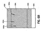
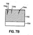
302,304,702・・・予め存在している堆積物
306,508,606,704・・・クラック
500・・・清浄なチャンバー部品
502,602,608,706・・・パーティクル抑制膜
504,604,610,708・・・新しい堆積物
Claims (30)
- 処理システムの処理チャンバーのためのチャンバー洗浄工程間の時間を延長する方法であって、
処理チャンバーの中に1つ以上の第1の基板を導入するステップと、
前記処理チャンバーの中で前記1つ以上の第1の基板上に第1の製造工程を実施するステップであって、第1の膜状堆積物が前記処理チャンバー内のチャンバー部品上に形成されるステップと、
前記1つ以上の第1の基板を前記処理チャンバーから取り出すステップと、
前記処理チャンバー内の前記チャンバー部品を反応ガスに暴露し、パーティクル抑制膜を形成するステップであって、前記パーティクル抑制膜は、前記チャンバー部品上に存在している第1の膜状堆積物の少なくとも一部から形成された酸化膜または酸化窒化膜であるステップと、
前記処理チャンバー内に1つ以上の第2の基板を導入するステップと、
前記処理チャンバー内で前記1つ以上の第2の基板上に第2の製造工程を実行するステップであって、新しい膜状堆積物が前記パーティクル抑制膜の上に形成され、前記パーティクル抑制膜は、前記1つ以上の第2の基板の処理の間に、前記処理チャンバーの中における、前記第1の膜状堆積物又は前記新しい膜状堆積物のうちの一方もしくは両方からのパーティクル形成を抑制するステップと、
前記処理チャンバーから前記1つ以上の第2の基板を取り出すステップと、
を備えていることを特徴とする方法。 - 前記チャンバー部品は、処理チューブ、壁部、ガス供給ライン、マニホールド、又は基板支持部材、もしくはこれらのうちの二以上の組み合わせであることを特徴とする請求項1に記載の方法。
- 前記パーティクル抑制膜は、酸化膜であることを特徴とする請求項1に記載の方法。
- 前記パーティクル抑制膜は、SiO2膜であることを特徴とする請求項1に記載の方法。
- 処理システムの処理チャンバーのためのチャンバー洗浄工程間の時間を延長する方法であって、
処理チャンバーの中に1つ以上の第1の基板を導入するステップと、
前記処理チャンバーの中で前記1つ以上の第1の基板上に第1の製造工程を実施するステップであって、第1の膜状堆積物が前記処理チャンバー内のチャンバー部品上に形成されるステップと、
前記1つ以上の第1の基板を前記処理チャンバーから取り出すステップと、
前記処理チャンバー内の前記チャンバー部品を反応ガスに暴露し、パーティクル抑制膜を形成するステップであって、前記パーティクル抑制膜は、前記チャンバー部品上に存在している第1の膜状堆積物の少なくとも一部から形成された窒化膜、酸化膜または酸化窒化膜であるステップと、
前記処理チャンバー内に1つ以上の第2の基板を導入するステップと、
前記処理チャンバー内で前記1つ以上の第2の基板上に第2の製造工程を実行するステップであって、新しい膜状堆積物が前記パーティクル抑制膜の上に形成され、前記パーティクル抑制膜は、前記1つ以上の第2の基板の処理の間に、前記処理チャンバーの中における、前記第1の膜状堆積物又は前記新しい膜状堆積物のうちの一方もしくは両方からのパーティクル形成を抑制するステップと、
前記処理チャンバーから前記1つ以上の第2の基板を取り出すステップと、
を備え、前記方法が、前記チャンバー部品の温度を第1の温度から第2の温度へ昇温するステップ及び前記チャンバー部品を前記第2の温度で反応ガスに暴露するステップと、
前記1つ以上の第2の基板を導入する前に、前記チャンバー部品の温度を前記第1の温度まで下げるステップと、
をさらに含むことを特徴とする方法。 - 前記反応ガスは、H2O、O2、O3、N2、NO、N2O、NO2、及びNH3からなるグループから選択された少なくとも一のガスを含有し、前記第1の膜状堆積物の少なくとも一部から化学的に転換させることによって窒化膜、酸化膜又は酸化窒化膜を形成し、前記第1の膜状堆積物の膜応力を減少させることを特徴とする請求項5に記載の方法。
- 前記暴露は、10ミリトール〜100トールの処理チャンバー圧力で行われることを特徴とする請求項5に記載の方法。
- 前記暴露は、前記1つ以上の第2の基板を導入する前に、前記処理チャンバーをパージし、排気するステップをさらに含むことを特徴とする請求項5に記載の方法。
- 前記暴露、前記パージ、及び前記排気のステップは、少なくとも一度繰り返されることを特徴とする請求項8に記載の方法。
- 前記第1の温度は、400℃〜800℃にあることを特徴とする請求項5に記載の方法。
- 前記第2の温度は、前記第1の温度より、100℃〜300℃高いことを特徴とする請求項5に記載の方法。
- 前記チャンバー部品の温度が前記第1の温度まで復帰する前に、前記チャンバー部品の温度を前記第2の温度から前記第1の温度より低い温度まで下げるステップをさらに含むことを特徴とする請求項5に記載の方法。
- 前記第1及び第2の製造工程の実施は、SiNの製造工程の実施を含み、前記第1の膜状堆積物及び新しい膜状堆積物は、SiNであることを特徴とする請求項1に記載の方法。
- 前記第1及び第2の製造工程の実施は、さらに前記処理チャンバー圧力を100トール以下にするステップを含むことを特徴とする請求項1に記載の方法。
- 前記第1及び第2の製造工程の実施は、さらに前記処理チャンバー圧力を1トール以下にするステップを含むことを特徴とする請求項1に記載の方法。
- 前記暴露するステップ、前記1つ以上の第2の基板を導入するステップ、前記第2の製造工程を実施するステップ、及び前記1つ以上の第2の基板を取り出すステップからなる一連のステップを、少なくとも一回繰り返すステップをさらに含むことを特徴とする請求項1に記載の方法。
- 前記1つ以上の第2の基板を導入するステップ、前記第2の製造工程を実施するステップ、及び前記1つ以上の第2の基板を取り出すステップからなる一連のステップを、少なくとも一回、前記処理チャンバー内のパーティクルレベルが前もって決められたレベルを超えるまで繰り返すステップをさらに含むことを特徴とする請求項1に記載の方法。
- 前記第2の製造工程を実施するステップは、前記処理チャンバー内でSiN製造処理を実施するステップであって、前記新しい膜状堆積物は前記SiO2膜の上に形成されたSiN蒸着材料であり、前記SiO2膜は、基板処理の間に、前記処理チャンバーの中において、前記第1の膜状堆積物又は前記SiN堆積物のうちの一方、もしくは両方からのパーティクル形成を抑制する、ステップを備えていることを特徴とする請求項4に記載の方法。
- 前記SiN製造工程は、前記1つ以上の第2の基板を有機シランベースの前躯体及び窒素を含有するガスに暴露し、前記1つ以上の第2の基板上にSiNを形成させるステップを含むことを特徴とする請求項18に記載の方法。
- 前記SiN製造工程は、前記1つ以上の第2の基板をビスターシャリーブチルアミノシラン前躯体にアンモニアガスの存在下で暴露し、前記1つ以上の第2の基板上にSiNを形成させるステップを含むことを特徴とする請求項18に記載の方法。
- 前記第2の製造工程を実施するステップは、前記処理チャンバー内でSiN製造工程を実施するステップであって、新しい膜状の堆積物は、パーティクル抑制膜上に形成されたSiN堆積物である、ステップを備えることを特徴とする請求項6に記載の方法。
- 前記SiN製造工程は、前記1つ以上の第2の基板を有機シランベースの前躯体及び窒素を含有するガスに暴露し、前記1つ以上の第2の基板上にSiNを堆積させるステップを含むことを特徴とする請求項21に記載の方法。
- 前記SiN製造工程は、前記1つ以上の第2の基板をビスターシャリーブチルアミノシラン前躯体にアンモニアガスの存在下で暴露し、前記1つ以上の第2の基板上にSiNを堆積させるステップを含むことを特徴とする請求項21に記載の方法。
- 処理システムの処理チャンバーのためのチャンバー洗浄工程間の時間を延長する方法であって、
前記処理チャンバーの中に1つ以上の第1の基板を導入し、前記処理チャンバー内のチャンバー部品を第1の温度まで加熱するステップと、
前記処理チャンバーの中で前記1つ以上の第1の基板上に前記第1の温度で第1の製造工程を実施するステップであって、第1の膜状堆積物が前記処理チャンバー内のチャンバー部品上に形成されるステップと、
前記1つ以上の第1の基板を前記処理チャンバーから取り出すステップと、
前記処理チャンバー内の前記チャンバー部品の温度を前記第1の温度より高い第2の温度まで昇温するステップと、
前記処理チャンバー内の前記チャンバー部品上の前記第1の膜状堆積物を前記第2の温度で反応ガスに暴露するステップであって、前記反応ガスはH2O、O2、O3、N2、NO、N2O、NO2、及びNH3のうちの少なくとも1つを含有し、前記第1の膜状堆積物の少なくとも一部を化学的に転換し、前記チャンバー部品上に窒化膜、酸化膜、または酸化窒化膜のパーティクル抑制膜を形成する、ステップと、
前記処理チャンバー内の前記チャンバー部品を前記第1の温度まで下げるステップと、
前記処理チャンバーの中に1つ以上の第2の基板を導入するステップと、
前記処理チャンバー内の前記1つ以上の第2の基板上に前記第1の温度で製造工程を実行するステップであって、新しい膜状堆積物が前記パーティクル抑制膜の上に形成され、前記パーティクル抑制膜は、前記1つ以上の第2の基板の処理の間に、前記処理チャンバーの中における、前記第1の膜状堆積物又は前記新しい膜状堆積物のうちの一方、もしくは両方からのパーティクル形成を抑制するステップと、
前記処理チャンバーから前記1つ以上の第2の基板を取り出すステップと、
を備えていることを特徴とする方法。 - 前記チャンバー部品は、処理チューブ、壁部、ガス供給ライン、マニホールド、又は基板支持部材、若しくはこれらのうちの二以上の組み合わせであることを特徴とする請求項24に記載の方法。
- 前記第1の温度は、400℃〜800℃にあることを特徴とする請求項24に記載の方法。
- 前記第2の温度は、前記第1の温度より100℃〜300℃高いことを特徴とする請求項24に記載の方法。
- 前記チャンバー部品を前記第1の温度まで下げるステップは、前記チャンバー部品を前記第2の温度から前記第1の温度より低い第3の温度まで下げ、次いで前記チャンバー部品の温度を前記第1の温度へ戻すステップを含むことを特徴とする請求項24に記載の方法。
- 前記第1及び第2の製造工程を実施するステップはSiN製造工程を実施するステップであって、前記第1の膜状堆積物及び前記新しい膜状堆積物がSiNである、ステップを備えることを特徴とする請求項24に記載の方法。
- 前記1つ以上の第2の基板を導入するステップ、前記第2の製造工程を実施するステップ、及び前記1つ以上の第2の基板を取り出すステップを、少なくとも一回、前記処理チャンバー内のパーティクルレベルが前もって決められたレベルを超えるまで繰り返すステップをさらに含むことを特徴とする請求項24に記載の方法。
Applications Claiming Priority (3)
| Application Number | Priority Date | Filing Date | Title |
|---|---|---|---|
| US10/814,713 US7604841B2 (en) | 2004-03-31 | 2004-03-31 | Method for extending time between chamber cleaning processes |
| US10/814,713 | 2004-03-31 | ||
| PCT/US2005/002509 WO2005104207A1 (en) | 2004-03-31 | 2005-01-26 | Method for extending time between chamber cleaning processes |
Publications (3)
| Publication Number | Publication Date |
|---|---|
| JP2007531304A JP2007531304A (ja) | 2007-11-01 |
| JP2007531304A5 JP2007531304A5 (ja) | 2008-03-13 |
| JP5219505B2 true JP5219505B2 (ja) | 2013-06-26 |
Family
ID=34960384
Family Applications (1)
| Application Number | Title | Priority Date | Filing Date |
|---|---|---|---|
| JP2007506147A Expired - Fee Related JP5219505B2 (ja) | 2004-03-31 | 2005-01-26 | チャンバー洗浄工程間の時間を延長する方法 |
Country Status (4)
| Country | Link |
|---|---|
| US (1) | US7604841B2 (ja) |
| JP (1) | JP5219505B2 (ja) |
| TW (1) | TW200536947A (ja) |
| WO (1) | WO2005104207A1 (ja) |
Families Citing this family (16)
| Publication number | Priority date | Publication date | Assignee | Title |
|---|---|---|---|---|
| JP4426518B2 (ja) * | 2005-10-11 | 2010-03-03 | 東京エレクトロン株式会社 | 処理装置 |
| JP4866658B2 (ja) * | 2006-05-23 | 2012-02-01 | 東京エレクトロン株式会社 | 半導体製造装置 |
| JP4245012B2 (ja) * | 2006-07-13 | 2009-03-25 | 東京エレクトロン株式会社 | 処理装置及びこのクリーニング方法 |
| JP5008957B2 (ja) | 2006-11-30 | 2012-08-22 | 東京エレクトロン株式会社 | シリコン窒化膜の形成方法、形成装置、形成装置の処理方法及びプログラム |
| KR100809852B1 (ko) * | 2007-05-17 | 2008-03-04 | (주)엘오티베큠 | 일체형 진공발생장치 |
| CN102270579A (zh) * | 2010-06-04 | 2011-12-07 | 中芯国际集成电路制造(上海)有限公司 | 一种遮挡晶片制备方法 |
| US8590705B2 (en) * | 2010-06-11 | 2013-11-26 | Air Products And Chemicals, Inc. | Cylinder surface treated container for monochlorosilane |
| JP2014209558A (ja) * | 2013-03-27 | 2014-11-06 | 東京エレクトロン株式会社 | シリコン酸化膜の形成方法、及び、シリコン酸化膜の形成装置 |
| US9828672B2 (en) | 2015-03-26 | 2017-11-28 | Lam Research Corporation | Minimizing radical recombination using ALD silicon oxide surface coating with intermittent restoration plasma |
| US10121655B2 (en) | 2015-11-20 | 2018-11-06 | Applied Materials, Inc. | Lateral plasma/radical source |
| CN107099782A (zh) * | 2016-02-23 | 2017-08-29 | 常州国成新材料科技有限公司 | 一种制备石墨烯、六角氮化硼等薄膜材料的化学气相沉积装置 |
| JP6648627B2 (ja) | 2016-04-27 | 2020-02-14 | 三菱電機株式会社 | 炭化珪素エピタキシャルウエハの製造方法、炭化珪素半導体装置の製造方法及び炭化珪素エピタキシャルウエハの製造装置 |
| CN108165953B (zh) * | 2017-12-25 | 2020-06-30 | 上海华力微电子有限公司 | 改善hto厚度稳定性的方法 |
| US20210340670A1 (en) * | 2018-10-19 | 2021-11-04 | Lam Research Corporation | In situ protective coating of chamber components for semiconductor processing |
| JP7076499B2 (ja) * | 2020-06-22 | 2022-05-27 | 株式会社Kokusai Electric | 基板処理装置、半導体装置の製造方法およびプログラム |
| CN113889403A (zh) * | 2021-12-08 | 2022-01-04 | 陕西亚成微电子股份有限公司 | 一种栅氧化层生长方法 |
Family Cites Families (21)
| Publication number | Priority date | Publication date | Assignee | Title |
|---|---|---|---|---|
| JP2605465B2 (ja) * | 1990-08-31 | 1997-04-30 | 日本電気株式会社 | 容量絶縁膜の形成方法 |
| DE69323716T2 (de) * | 1993-01-28 | 1999-08-19 | Applied Materials Inc | Verfahren zur CVD-Beschichtung einer Mehrschichtstruktur in einer einzigen Kammer |
| JPH09167755A (ja) * | 1995-12-15 | 1997-06-24 | Nec Corp | プラズマ酸化膜処理装置 |
| US5824375A (en) * | 1996-10-24 | 1998-10-20 | Applied Materials, Inc. | Decontamination of a plasma reactor using a plasma after a chamber clean |
| US6950193B1 (en) * | 1997-10-28 | 2005-09-27 | Rockwell Automation Technologies, Inc. | System for monitoring substrate conditions |
| US6090705A (en) * | 1998-01-20 | 2000-07-18 | Tokyo Electron Limited | Method of eliminating edge effect in chemical vapor deposition of a metal |
| JP3959203B2 (ja) * | 1999-05-21 | 2007-08-15 | 新日本無線株式会社 | 半導体装置の製造方法 |
| TW440952B (en) * | 1999-07-12 | 2001-06-16 | Lam Res Co Ltd | Waferless clean process of dry etcher |
| US6426015B1 (en) * | 1999-12-14 | 2002-07-30 | Applied Materials, Inc. | Method of reducing undesired etching of insulation due to elevated boron concentrations |
| US6468903B2 (en) | 2000-11-15 | 2002-10-22 | Asm International N.V. | Pre-treatment of reactor parts for chemical vapor deposition reactors |
| JP2002158218A (ja) * | 2000-11-21 | 2002-05-31 | Toshiba Corp | 成膜方法 |
| US6413321B1 (en) * | 2000-12-07 | 2002-07-02 | Applied Materials, Inc. | Method and apparatus for reducing particle contamination on wafer backside during CVD process |
| US6805952B2 (en) | 2000-12-29 | 2004-10-19 | Lam Research Corporation | Low contamination plasma chamber components and methods for making the same |
| US6589868B2 (en) | 2001-02-08 | 2003-07-08 | Applied Materials, Inc. | Si seasoning to reduce particles, extend clean frequency, block mobile ions and increase chamber throughput |
| JP4897159B2 (ja) | 2001-08-03 | 2012-03-14 | 株式会社日立国際電気 | 半導体装置の製造方法 |
| JP4700236B2 (ja) | 2001-08-03 | 2011-06-15 | 株式会社日立国際電気 | 半導体装置の製造方法および基板処理装置 |
| JP2003100743A (ja) | 2001-09-26 | 2003-04-04 | Hitachi Kokusai Electric Inc | 半導体デバイスの製造方法 |
| JP2003188159A (ja) * | 2001-12-19 | 2003-07-04 | Seiko Epson Corp | Cvd装置及び半導体装置の製造方法 |
| JP2004153066A (ja) * | 2002-10-31 | 2004-05-27 | Fujitsu Ltd | 半導体装置の製造方法 |
| US7371427B2 (en) * | 2003-05-20 | 2008-05-13 | Applied Materials, Inc. | Reduction of hillocks prior to dielectric barrier deposition in Cu damascene |
| US20060093756A1 (en) * | 2004-11-03 | 2006-05-04 | Nagarajan Rajagopalan | High-power dielectric seasoning for stable wafer-to-wafer thickness uniformity of dielectric CVD films |
-
2004
- 2004-03-31 US US10/814,713 patent/US7604841B2/en not_active Expired - Fee Related
-
2005
- 2005-01-26 JP JP2007506147A patent/JP5219505B2/ja not_active Expired - Fee Related
- 2005-01-26 WO PCT/US2005/002509 patent/WO2005104207A1/en active Application Filing
- 2005-03-31 TW TW094110235A patent/TW200536947A/zh unknown
Also Published As
| Publication number | Publication date |
|---|---|
| WO2005104207A1 (en) | 2005-11-03 |
| US20050221001A1 (en) | 2005-10-06 |
| JP2007531304A (ja) | 2007-11-01 |
| TW200536947A (en) | 2005-11-16 |
| US7604841B2 (en) | 2009-10-20 |
Similar Documents
| Publication | Publication Date | Title |
|---|---|---|
| JP5219505B2 (ja) | チャンバー洗浄工程間の時間を延長する方法 | |
| US7205187B2 (en) | Micro-feature fill process and apparatus using hexachlorodisilane or other chlorine-containing silicon precursor | |
| US7509962B2 (en) | Method and control system for treating a hafnium-based dielectric processing system | |
| JP6671262B2 (ja) | 窒化膜の形成方法および形成装置 | |
| US8178448B2 (en) | Film formation method and apparatus for semiconductor process | |
| US7351668B2 (en) | Film formation method and apparatus for semiconductor process | |
| KR101076470B1 (ko) | 반도체 장치 및 그 제조 방법 | |
| CN111593329A (zh) | 包括处理步骤的循环沉积方法及用于其的装置 | |
| US20080063791A1 (en) | Film formation method and apparatus for semiconductor process | |
| JP6047039B2 (ja) | 半導体装置の製造方法、基板処理方法、基板処理装置およびプログラム | |
| US20050056219A1 (en) | Formation of a metal-containing film by sequential gas exposure in a batch type processing system | |
| WO2004066377A1 (ja) | 被処理基板上にシリコン窒化膜を形成するcvd方法 | |
| CN105225926A (zh) | 清洁方法、半导体器件的制造方法及衬底处理装置 | |
| US20220277952A1 (en) | Substrate Processing Apparatus, Method of Manufacturing Semiconductor Device and Non-transitory Computer-readable Recording Medium | |
| US20060068606A1 (en) | Method and apparatus for forming silicon nitride film | |
| US20130102161A1 (en) | Method of Manufacturing Semiconductor Device, Cleaning Method, Substrate Processing Apparatus and Non-Transitory Computer-Readable Recording Medium | |
| CN108695149B (zh) | 蚀刻方法、蚀刻装置以及存储介质 | |
| JP6902958B2 (ja) | シリコン膜の形成方法および形成装置 | |
| CN101548375A (zh) | 半导体装置以及其制造方法 | |
| JP6987021B2 (ja) | プラズマ処理装置及びプラズマ処理方法 | |
| JP2014075491A (ja) | 半導体装置の製造方法、基板処理方法、基板処理装置、およびプログラム | |
| JPH07201738A (ja) | 薄膜形成前処理方法および薄膜形成方法 | |
| US20200095678A1 (en) | Method of cleaning, method of manufacturing semiconductor device, substrate processing apparatus, and recording medium | |
| US11380538B2 (en) | Method of forming nitride film and apparatus for forming nitride film | |
| JP6441989B2 (ja) | 半導体装置の製造方法、基板処理装置、プログラムおよび記録媒体 |
Legal Events
| Date | Code | Title | Description |
|---|---|---|---|
| A521 | Request for written amendment filed |
Free format text: JAPANESE INTERMEDIATE CODE: A523 Effective date: 20080123 |
|
| A621 | Written request for application examination |
Free format text: JAPANESE INTERMEDIATE CODE: A621 Effective date: 20080123 |
|
| A131 | Notification of reasons for refusal |
Free format text: JAPANESE INTERMEDIATE CODE: A131 Effective date: 20101214 |
|
| A601 | Written request for extension of time |
Free format text: JAPANESE INTERMEDIATE CODE: A601 Effective date: 20110314 |
|
| A602 | Written permission of extension of time |
Free format text: JAPANESE INTERMEDIATE CODE: A602 Effective date: 20110322 |
|
| A521 | Request for written amendment filed |
Free format text: JAPANESE INTERMEDIATE CODE: A523 Effective date: 20110407 |
|
| A131 | Notification of reasons for refusal |
Free format text: JAPANESE INTERMEDIATE CODE: A131 Effective date: 20111122 |
|
| A521 | Request for written amendment filed |
Free format text: JAPANESE INTERMEDIATE CODE: A523 Effective date: 20120222 |
|
| A131 | Notification of reasons for refusal |
Free format text: JAPANESE INTERMEDIATE CODE: A131 Effective date: 20121218 |
|
| A521 | Request for written amendment filed |
Free format text: JAPANESE INTERMEDIATE CODE: A523 Effective date: 20130107 |
|
| TRDD | Decision of grant or rejection written | ||
| A01 | Written decision to grant a patent or to grant a registration (utility model) |
Free format text: JAPANESE INTERMEDIATE CODE: A01 Effective date: 20130205 |
|
| A61 | First payment of annual fees (during grant procedure) |
Free format text: JAPANESE INTERMEDIATE CODE: A61 Effective date: 20130305 |
|
| FPAY | Renewal fee payment (event date is renewal date of database) |
Free format text: PAYMENT UNTIL: 20160315 Year of fee payment: 3 |
|
| R150 | Certificate of patent or registration of utility model |
Ref document number: 5219505 Country of ref document: JP Free format text: JAPANESE INTERMEDIATE CODE: R150 Free format text: JAPANESE INTERMEDIATE CODE: R150 |
|
| S111 | Request for change of ownership or part of ownership |
Free format text: JAPANESE INTERMEDIATE CODE: R313117 |
|
| R350 | Written notification of registration of transfer |
Free format text: JAPANESE INTERMEDIATE CODE: R350 |
|
| R250 | Receipt of annual fees |
Free format text: JAPANESE INTERMEDIATE CODE: R250 |
|
| R250 | Receipt of annual fees |
Free format text: JAPANESE INTERMEDIATE CODE: R250 |
|
| R250 | Receipt of annual fees |
Free format text: JAPANESE INTERMEDIATE CODE: R250 |
|
| LAPS | Cancellation because of no payment of annual fees |