JP5199072B2 - チャネル領域の平滑な表面を有するシリコンカーバイドデバイスを作製する方法 - Google Patents
チャネル領域の平滑な表面を有するシリコンカーバイドデバイスを作製する方法 Download PDFInfo
- Publication number
- JP5199072B2 JP5199072B2 JP2008513462A JP2008513462A JP5199072B2 JP 5199072 B2 JP5199072 B2 JP 5199072B2 JP 2008513462 A JP2008513462 A JP 2008513462A JP 2008513462 A JP2008513462 A JP 2008513462A JP 5199072 B2 JP5199072 B2 JP 5199072B2
- Authority
- JP
- Japan
- Prior art keywords
- region
- silicon carbide
- type
- layer
- channel region
- Prior art date
- Legal status (The legal status is an assumption and is not a legal conclusion. Google has not performed a legal analysis and makes no representation as to the accuracy of the status listed.)
- Active
Links
- 229910010271 silicon carbide Inorganic materials 0.000 title claims description 155
- HBMJWWWQQXIZIP-UHFFFAOYSA-N silicon carbide Chemical compound [Si+]#[C-] HBMJWWWQQXIZIP-UHFFFAOYSA-N 0.000 title claims description 140
- 238000000034 method Methods 0.000 title claims description 56
- 230000003746 surface roughness Effects 0.000 claims description 28
- 239000002019 doping agent Substances 0.000 claims description 24
- 239000000758 substrate Substances 0.000 claims description 23
- 230000008569 process Effects 0.000 claims description 20
- 230000005669 field effect Effects 0.000 claims description 13
- 239000004065 semiconductor Substances 0.000 claims description 13
- 230000009467 reduction Effects 0.000 claims description 11
- 229910044991 metal oxide Inorganic materials 0.000 claims description 6
- 150000004706 metal oxides Chemical class 0.000 claims description 6
- 239000000126 substance Substances 0.000 claims description 4
- 238000005498 polishing Methods 0.000 claims description 3
- 238000005530 etching Methods 0.000 claims description 2
- 230000003213 activating effect Effects 0.000 claims 1
- 108091006146 Channels Proteins 0.000 description 63
- 238000002513 implantation Methods 0.000 description 11
- 238000009792 diffusion process Methods 0.000 description 9
- 239000007943 implant Substances 0.000 description 9
- 238000004519 manufacturing process Methods 0.000 description 9
- 230000015572 biosynthetic process Effects 0.000 description 7
- XUIMIQQOPSSXEZ-UHFFFAOYSA-N Silicon Chemical compound [Si] XUIMIQQOPSSXEZ-UHFFFAOYSA-N 0.000 description 6
- 239000011810 insulating material Substances 0.000 description 6
- 229910052710 silicon Inorganic materials 0.000 description 6
- 239000010703 silicon Substances 0.000 description 6
- 229910052751 metal Inorganic materials 0.000 description 5
- 239000002184 metal Substances 0.000 description 5
- IJGRMHOSHXDMSA-UHFFFAOYSA-N Atomic nitrogen Chemical compound N#N IJGRMHOSHXDMSA-UHFFFAOYSA-N 0.000 description 4
- VYPSYNLAJGMNEJ-UHFFFAOYSA-N Silicium dioxide Chemical compound O=[Si]=O VYPSYNLAJGMNEJ-UHFFFAOYSA-N 0.000 description 4
- 239000000463 material Substances 0.000 description 4
- 229910052782 aluminium Inorganic materials 0.000 description 3
- XAGFODPZIPBFFR-UHFFFAOYSA-N aluminium Chemical compound [Al] XAGFODPZIPBFFR-UHFFFAOYSA-N 0.000 description 3
- 238000000137 annealing Methods 0.000 description 3
- 239000012212 insulator Substances 0.000 description 3
- 238000005468 ion implantation Methods 0.000 description 3
- PXHVJJICTQNCMI-UHFFFAOYSA-N Nickel Chemical compound [Ni] PXHVJJICTQNCMI-UHFFFAOYSA-N 0.000 description 2
- MWUXSHHQAYIFBG-UHFFFAOYSA-N Nitric oxide Chemical compound O=[N] MWUXSHHQAYIFBG-UHFFFAOYSA-N 0.000 description 2
- 230000004913 activation Effects 0.000 description 2
- 238000002347 injection Methods 0.000 description 2
- 239000007924 injection Substances 0.000 description 2
- 229910021421 monocrystalline silicon Inorganic materials 0.000 description 2
- 229910052757 nitrogen Inorganic materials 0.000 description 2
- 238000000059 patterning Methods 0.000 description 2
- 235000012239 silicon dioxide Nutrition 0.000 description 2
- 239000000377 silicon dioxide Substances 0.000 description 2
- UFHFLCQGNIYNRP-UHFFFAOYSA-N Hydrogen Chemical compound [H][H] UFHFLCQGNIYNRP-UHFFFAOYSA-N 0.000 description 1
- ZOKXTWBITQBERF-UHFFFAOYSA-N Molybdenum Chemical compound [Mo] ZOKXTWBITQBERF-UHFFFAOYSA-N 0.000 description 1
- 102000004129 N-Type Calcium Channels Human genes 0.000 description 1
- 108090000699 N-Type Calcium Channels Proteins 0.000 description 1
- OAICVXFJPJFONN-UHFFFAOYSA-N Phosphorus Chemical compound [P] OAICVXFJPJFONN-UHFFFAOYSA-N 0.000 description 1
- 229910004298 SiO 2 Inorganic materials 0.000 description 1
- 229910001069 Ti alloy Inorganic materials 0.000 description 1
- 239000000969 carrier Substances 0.000 description 1
- 230000015556 catabolic process Effects 0.000 description 1
- 230000008859 change Effects 0.000 description 1
- 238000000151 deposition Methods 0.000 description 1
- 239000003989 dielectric material Substances 0.000 description 1
- 230000005684 electric field Effects 0.000 description 1
- 229910052739 hydrogen Inorganic materials 0.000 description 1
- 239000001257 hydrogen Substances 0.000 description 1
- 238000011835 investigation Methods 0.000 description 1
- 150000002500 ions Chemical class 0.000 description 1
- 229910052750 molybdenum Inorganic materials 0.000 description 1
- 239000011733 molybdenum Substances 0.000 description 1
- 229910052759 nickel Inorganic materials 0.000 description 1
- 238000002161 passivation Methods 0.000 description 1
- 229910052698 phosphorus Inorganic materials 0.000 description 1
- 239000011574 phosphorus Substances 0.000 description 1
- 238000007517 polishing process Methods 0.000 description 1
- 229910021420 polycrystalline silicon Inorganic materials 0.000 description 1
- 229920005591 polysilicon Polymers 0.000 description 1
- 239000004071 soot Substances 0.000 description 1
Images


Classifications
-
- H—ELECTRICITY
- H01—ELECTRIC ELEMENTS
- H01L—SEMICONDUCTOR DEVICES NOT COVERED BY CLASS H10
- H01L29/00—Semiconductor devices adapted for rectifying, amplifying, oscillating or switching, or capacitors or resistors with at least one potential-jump barrier or surface barrier, e.g. PN junction depletion layer or carrier concentration layer; Details of semiconductor bodies or of electrodes thereof ; Multistep manufacturing processes therefor
- H01L29/66—Types of semiconductor device ; Multistep manufacturing processes therefor
- H01L29/68—Types of semiconductor device ; Multistep manufacturing processes therefor controllable by only the electric current supplied, or only the electric potential applied, to an electrode which does not carry the current to be rectified, amplified or switched
- H01L29/76—Unipolar devices, e.g. field effect transistors
- H01L29/772—Field effect transistors
- H01L29/78—Field effect transistors with field effect produced by an insulated gate
- H01L29/7801—DMOS transistors, i.e. MISFETs with a channel accommodating body or base region adjoining a drain drift region
- H01L29/7802—Vertical DMOS transistors, i.e. VDMOS transistors
-
- H—ELECTRICITY
- H01—ELECTRIC ELEMENTS
- H01L—SEMICONDUCTOR DEVICES NOT COVERED BY CLASS H10
- H01L29/00—Semiconductor devices adapted for rectifying, amplifying, oscillating or switching, or capacitors or resistors with at least one potential-jump barrier or surface barrier, e.g. PN junction depletion layer or carrier concentration layer; Details of semiconductor bodies or of electrodes thereof ; Multistep manufacturing processes therefor
- H01L29/02—Semiconductor bodies ; Multistep manufacturing processes therefor
- H01L29/06—Semiconductor bodies ; Multistep manufacturing processes therefor characterised by their shape; characterised by the shapes, relative sizes, or dispositions of the semiconductor regions ; characterised by the concentration or distribution of impurities within semiconductor regions
- H01L29/08—Semiconductor bodies ; Multistep manufacturing processes therefor characterised by their shape; characterised by the shapes, relative sizes, or dispositions of the semiconductor regions ; characterised by the concentration or distribution of impurities within semiconductor regions with semiconductor regions connected to an electrode carrying current to be rectified, amplified or switched and such electrode being part of a semiconductor device which comprises three or more electrodes
- H01L29/0843—Source or drain regions of field-effect devices
- H01L29/0847—Source or drain regions of field-effect devices of field-effect transistors with insulated gate
- H01L29/0852—Source or drain regions of field-effect devices of field-effect transistors with insulated gate of DMOS transistors
- H01L29/0873—Drain regions
- H01L29/0878—Impurity concentration or distribution
-
- H—ELECTRICITY
- H01—ELECTRIC ELEMENTS
- H01L—SEMICONDUCTOR DEVICES NOT COVERED BY CLASS H10
- H01L29/00—Semiconductor devices adapted for rectifying, amplifying, oscillating or switching, or capacitors or resistors with at least one potential-jump barrier or surface barrier, e.g. PN junction depletion layer or carrier concentration layer; Details of semiconductor bodies or of electrodes thereof ; Multistep manufacturing processes therefor
- H01L29/02—Semiconductor bodies ; Multistep manufacturing processes therefor
- H01L29/06—Semiconductor bodies ; Multistep manufacturing processes therefor characterised by their shape; characterised by the shapes, relative sizes, or dispositions of the semiconductor regions ; characterised by the concentration or distribution of impurities within semiconductor regions
- H01L29/08—Semiconductor bodies ; Multistep manufacturing processes therefor characterised by their shape; characterised by the shapes, relative sizes, or dispositions of the semiconductor regions ; characterised by the concentration or distribution of impurities within semiconductor regions with semiconductor regions connected to an electrode carrying current to be rectified, amplified or switched and such electrode being part of a semiconductor device which comprises three or more electrodes
- H01L29/0843—Source or drain regions of field-effect devices
- H01L29/0847—Source or drain regions of field-effect devices of field-effect transistors with insulated gate
- H01L29/0852—Source or drain regions of field-effect devices of field-effect transistors with insulated gate of DMOS transistors
- H01L29/0873—Drain regions
- H01L29/0886—Shape
-
- H—ELECTRICITY
- H01—ELECTRIC ELEMENTS
- H01L—SEMICONDUCTOR DEVICES NOT COVERED BY CLASS H10
- H01L29/00—Semiconductor devices adapted for rectifying, amplifying, oscillating or switching, or capacitors or resistors with at least one potential-jump barrier or surface barrier, e.g. PN junction depletion layer or carrier concentration layer; Details of semiconductor bodies or of electrodes thereof ; Multistep manufacturing processes therefor
- H01L29/02—Semiconductor bodies ; Multistep manufacturing processes therefor
- H01L29/12—Semiconductor bodies ; Multistep manufacturing processes therefor characterised by the materials of which they are formed
- H01L29/16—Semiconductor bodies ; Multistep manufacturing processes therefor characterised by the materials of which they are formed including, apart from doping materials or other impurities, only elements of Group IV of the Periodic System
- H01L29/1608—Silicon carbide
-
- H—ELECTRICITY
- H01—ELECTRIC ELEMENTS
- H01L—SEMICONDUCTOR DEVICES NOT COVERED BY CLASS H10
- H01L29/00—Semiconductor devices adapted for rectifying, amplifying, oscillating or switching, or capacitors or resistors with at least one potential-jump barrier or surface barrier, e.g. PN junction depletion layer or carrier concentration layer; Details of semiconductor bodies or of electrodes thereof ; Multistep manufacturing processes therefor
- H01L29/66—Types of semiconductor device ; Multistep manufacturing processes therefor
- H01L29/66007—Multistep manufacturing processes
- H01L29/66053—Multistep manufacturing processes of devices having a semiconductor body comprising crystalline silicon carbide
- H01L29/66068—Multistep manufacturing processes of devices having a semiconductor body comprising crystalline silicon carbide the devices being controllable only by the electric current supplied or the electric potential applied, to an electrode which does not carry the current to be rectified, amplified or switched, e.g. three-terminal devices
-
- Y—GENERAL TAGGING OF NEW TECHNOLOGICAL DEVELOPMENTS; GENERAL TAGGING OF CROSS-SECTIONAL TECHNOLOGIES SPANNING OVER SEVERAL SECTIONS OF THE IPC; TECHNICAL SUBJECTS COVERED BY FORMER USPC CROSS-REFERENCE ART COLLECTIONS [XRACs] AND DIGESTS
- Y10—TECHNICAL SUBJECTS COVERED BY FORMER USPC
- Y10S—TECHNICAL SUBJECTS COVERED BY FORMER USPC CROSS-REFERENCE ART COLLECTIONS [XRACs] AND DIGESTS
- Y10S438/00—Semiconductor device manufacturing: process
- Y10S438/931—Silicon carbide semiconductor
Description
Claims (15)
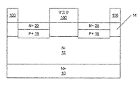
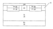
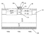
- シリコンカーバイドパワーデバイスを形成する方法であって、
シリコンカーバイド基板上にn−シリコンカーバイド層を形成するステップ、
前記n−シリコンカーバイド層上にp型シリコンカーバイドウェル領域を形成するために、前記n−シリコンカーバイド層内にp型ドーパントを注入するステップ、または、前記n−シリコンカーバイド層上にp型エピタキシャル層を形成するステップ、
前記p型シリコンカーバイドウェル領域内にp+シリコンカーバイドの埋込み領域を形成するために、前記p型シリコンカーバイドウェル領域内にp型ドーパントを注入するステップ、
n型ドーパントをp+シリコンカーバイドの埋込み領域上のp型シリコンカーバイドウェルにインプラントして、p+シリコンカーバイドの埋込み領域上に、シリコンカーバイドのn+領域を形成するステップであって、パワーデバイスのチャネル領域はp+の埋込み領域とシリコンカーバイドのn+領域に隣接し、
前記チャネル領域上に、再成長プロセスでn−シリコンカーバイドエピタキシャル領域を形成するステップ、および、
前記チャネル領域から前記n−領域の表面の一部分を化学機械研磨(CMP)プロセスで除去するステップであって、それにより、前記n−領域の一部分が、前記チャネル領域上に残って、前記チャネル領域の表面粗さを低減する、ことを特徴とする方法。 - 前記CMPプロセスは、前記チャネル領域から前記n−領域の、1000から5000Åを除く全てを除去することを特徴とする請求項1に記載の方法。
- 前記除去するステップは、前記チャネル領域の表面粗さの深さの2.0から3.0倍である前記n−領域の一部分を除去するステップをさらに含むことを特徴とする請求項1に記載の方法。
- 前記n−領域の1500Åは、前記CMPプロセス後に前記チャネル領域上に残ることを特徴とする請求項3に記載の方法。
- 前記表面粗さの低減は、28Åから1.0Åまでの2乗平均平方根(RMS)表面粗さの低減であることを特徴とする請求項1に記載の方法。
- 前記除去するステップは
前記チャネル領域上の前記n−領域の残りの部分上に、100から1000Åの厚さを有する犠牲酸化物層を形成するステップ、および、
前記犠牲酸化物層を除去するステップを続いて伴い、前記RMS表円面粗さは、前記犠牲酸化物層の形成および1.0Åから0.70Åまでの前記犠牲酸化物層の除去によってさらに低減されることを特徴とする請求項5に記載の方法。 - 前記n−領域を形成するステップは、前記チャネル領域上でn−エピタキシャル層を所定の厚さに成長させることであって、それにより、前記n−エピタキシャル層の一部分が、前記n−エピタキシャル層のその部分の除去後に、前記チャネル領域上に残るようにn−領域を成長させるステップを含むことを特徴とする請求項1に記載の方法。
- 前記n−エピタキシャル層の前記所定の厚さは、1500Åから6000Åであることを特徴とする請求項7に記載の方法。
- 前記CMPプロセスを実施するステップは、前記n−領域が、前記n+領域から除去されるように、前記n−領域を選択的にエッチングするステップを続いて伴うことを特徴とする請求項1に記載の方法。
- 前記注入されたドーパントを1600℃より高い温度にさらすことによって前記注入されたドーパントを活性化するステップをさらに含むことを特徴とする請求項1に記載の方法。
- 前記チャネル領域に隣接する前記p型シリコンカーバイドウェル領域内にシリコンカーバイドのn型領域を形成するステップをさらに含み、前記チャネル領域が、前記p+シリコンカーバイドの埋込み領域と前記シリコンカーバイドのn型領域との間に画定され、前記シリコンカーバイドのn型領域が、前記シリコンカーバイドパワーデバイスの接合型電界効果トランジスタ(Junction Field Effect Transistor)(JFET)領域であることを特徴とする請求項1に記載の方法。
- 前記チャネル領域に隣接する前記p型シリコンカーバイドウェル領域内にシリコンカーバイドのn型領域を形成するステップをさらに含み、前記チャネル領域が、前記p+シリコンカーバイドの埋込み領域と前記シリコンカーバイドのn型領域との間に画定され、前記n−領域が、前記チャネル領域上に残るだけであることを特徴とする請求項1に記載の方法。
- 前記基板は、前記シリコンカーバイドパワーデバイスのドリフト領域の役をするn−基板を含み、前記n−シリコンカーバイド層に対向するn+ドレイン領域を基板上に形成するステップをさらに含むことを特徴とする請求項1に記載の方法。
- 前記n+ドレイン領域を形成するステップは、前記n−基板内に前記n+ドレイン領域を注入するステップ、および、前記n−基板上で前記n+ドレイン領域を成長させるステップの少なくとも一方を含むことを特徴とする請求項13に記載の方法。
- 前記シリコンカーバイドパワーデバイスは、金属酸化物半導体電界効果トランジスタ(Metal Oxide Semiconductor Field Effect Transistor)(MOSFET)を含むことを特徴とする請求項1に記載の方法。
Applications Claiming Priority (3)
| Application Number | Priority Date | Filing Date | Title |
|---|---|---|---|
| US11/136,057 | 2005-05-24 | ||
| US11/136,057 US7528040B2 (en) | 2005-05-24 | 2005-05-24 | Methods of fabricating silicon carbide devices having smooth channels |
| PCT/US2006/009493 WO2006127093A2 (en) | 2005-05-24 | 2006-03-16 | Methods of fabricating silicon carbide devices having a smooth surface of the channel regions |
Related Child Applications (1)
| Application Number | Title | Priority Date | Filing Date |
|---|---|---|---|
| JP2012111459A Division JP6008571B2 (ja) | 2005-05-24 | 2012-05-15 | チャネル領域の平滑な表面を有するシリコンカーバイドデバイスを作製する方法 |
Publications (2)
| Publication Number | Publication Date |
|---|---|
| JP2008543048A JP2008543048A (ja) | 2008-11-27 |
| JP5199072B2 true JP5199072B2 (ja) | 2013-05-15 |
Family
ID=36753949
Family Applications (2)
| Application Number | Title | Priority Date | Filing Date |
|---|---|---|---|
| JP2008513462A Active JP5199072B2 (ja) | 2005-05-24 | 2006-03-16 | チャネル領域の平滑な表面を有するシリコンカーバイドデバイスを作製する方法 |
| JP2012111459A Active JP6008571B2 (ja) | 2005-05-24 | 2012-05-15 | チャネル領域の平滑な表面を有するシリコンカーバイドデバイスを作製する方法 |
Family Applications After (1)
| Application Number | Title | Priority Date | Filing Date |
|---|---|---|---|
| JP2012111459A Active JP6008571B2 (ja) | 2005-05-24 | 2012-05-15 | チャネル領域の平滑な表面を有するシリコンカーバイドデバイスを作製する方法 |
Country Status (5)
| Country | Link |
|---|---|
| US (4) | US7528040B2 (ja) |
| EP (2) | EP1883951B1 (ja) |
| JP (2) | JP5199072B2 (ja) |
| TW (2) | TWI404131B (ja) |
| WO (1) | WO2006127093A2 (ja) |
Families Citing this family (41)
| Publication number | Priority date | Publication date | Assignee | Title |
|---|---|---|---|---|
| US7569900B2 (en) * | 2004-11-16 | 2009-08-04 | Kabushiki Kaisha Toshiba | Silicon carbide high breakdown voltage semiconductor device |
| US8367510B2 (en) * | 2005-09-14 | 2013-02-05 | Central Research Institute Of Electric Power Industry | Process for producing silicon carbide semiconductor device |
| EP2674966B1 (en) * | 2006-06-29 | 2019-10-23 | Cree, Inc. | Silicon carbide switching devices including P-type channels |
| US8272781B2 (en) * | 2006-08-01 | 2012-09-25 | Intel Corporation | Dynamic power control of a memory device thermal sensor |
| US8432012B2 (en) | 2006-08-01 | 2013-04-30 | Cree, Inc. | Semiconductor devices including schottky diodes having overlapping doped regions and methods of fabricating same |
| US7728402B2 (en) * | 2006-08-01 | 2010-06-01 | Cree, Inc. | Semiconductor devices including schottky diodes with controlled breakdown |
| WO2008020911A2 (en) * | 2006-08-17 | 2008-02-21 | Cree, Inc. | High power insulated gate bipolar transistors |
| JP5071763B2 (ja) * | 2006-10-16 | 2012-11-14 | 独立行政法人産業技術総合研究所 | 炭化ケイ素半導体装置およびその製造方法 |
| US7781312B2 (en) * | 2006-12-13 | 2010-08-24 | General Electric Company | Silicon carbide devices and method of making |
| US8835987B2 (en) * | 2007-02-27 | 2014-09-16 | Cree, Inc. | Insulated gate bipolar transistors including current suppressing layers |
| JP4700045B2 (ja) * | 2007-11-13 | 2011-06-15 | Okiセミコンダクタ株式会社 | 半導体素子の製造方法 |
| US7795691B2 (en) * | 2008-01-25 | 2010-09-14 | Cree, Inc. | Semiconductor transistor with P type re-grown channel layer |
| TWI364798B (en) * | 2008-03-21 | 2012-05-21 | Vanguard Int Semiconduct Corp | Semiconductor device and fabrication method thereof |
| US8232558B2 (en) | 2008-05-21 | 2012-07-31 | Cree, Inc. | Junction barrier Schottky diodes with current surge capability |
| US8294507B2 (en) | 2009-05-08 | 2012-10-23 | Cree, Inc. | Wide bandgap bipolar turn-off thyristor having non-negative temperature coefficient and related control circuits |
| US8629509B2 (en) * | 2009-06-02 | 2014-01-14 | Cree, Inc. | High voltage insulated gate bipolar transistors with minority carrier diverter |
| US8193848B2 (en) | 2009-06-02 | 2012-06-05 | Cree, Inc. | Power switching devices having controllable surge current capabilities |
| US8541787B2 (en) * | 2009-07-15 | 2013-09-24 | Cree, Inc. | High breakdown voltage wide band-gap MOS-gated bipolar junction transistors with avalanche capability |
| JP5474068B2 (ja) * | 2009-07-24 | 2014-04-16 | 三菱電機株式会社 | 炭化珪素半導体装置の製造方法 |
| US8354690B2 (en) | 2009-08-31 | 2013-01-15 | Cree, Inc. | Solid-state pinch off thyristor circuits |
| US9117739B2 (en) | 2010-03-08 | 2015-08-25 | Cree, Inc. | Semiconductor devices with heterojunction barrier regions and methods of fabricating same |
| US8415671B2 (en) | 2010-04-16 | 2013-04-09 | Cree, Inc. | Wide band-gap MOSFETs having a heterojunction under gate trenches thereof and related methods of forming such devices |
| US9142662B2 (en) | 2011-05-06 | 2015-09-22 | Cree, Inc. | Field effect transistor devices with low source resistance |
| US9673283B2 (en) | 2011-05-06 | 2017-06-06 | Cree, Inc. | Power module for supporting high current densities |
| US9029945B2 (en) | 2011-05-06 | 2015-05-12 | Cree, Inc. | Field effect transistor devices with low source resistance |
| US8618582B2 (en) | 2011-09-11 | 2013-12-31 | Cree, Inc. | Edge termination structure employing recesses for edge termination elements |
| US8664665B2 (en) | 2011-09-11 | 2014-03-04 | Cree, Inc. | Schottky diode employing recesses for elements of junction barrier array |
| US8680587B2 (en) | 2011-09-11 | 2014-03-25 | Cree, Inc. | Schottky diode |
| US9640617B2 (en) | 2011-09-11 | 2017-05-02 | Cree, Inc. | High performance power module |
| US9373617B2 (en) | 2011-09-11 | 2016-06-21 | Cree, Inc. | High current, low switching loss SiC power module |
| DE102013010187A1 (de) | 2012-06-27 | 2014-01-02 | Fairchild Semiconductor Corp. | Schottky-Barriere-Vorrichtung mit lokal planarisierter Oberfläche und zugehöriges Halbleitererzeugnis |
| JP5961563B2 (ja) * | 2013-01-25 | 2016-08-02 | 株式会社豊田中央研究所 | 半導体装置の製造方法 |
| JP2015041644A (ja) * | 2013-08-20 | 2015-03-02 | 富士電機株式会社 | Mos型半導体装置の製造方法 |
| JP6347188B2 (ja) * | 2014-09-08 | 2018-06-27 | 富士電機株式会社 | 炭化珪素半導体装置の製造方法および炭化珪素半導体装置 |
| US9685550B2 (en) * | 2014-12-26 | 2017-06-20 | Fairchild Semiconductor Corporation | Silicon carbide (SiC) device with improved gate dielectric shielding |
| JP6351874B2 (ja) * | 2015-12-02 | 2018-07-04 | 三菱電機株式会社 | 炭化珪素エピタキシャル基板および炭化珪素半導体装置 |
| JP6237845B1 (ja) * | 2016-08-24 | 2017-11-29 | 富士電機株式会社 | 縦型mosfetおよび縦型mosfetの製造方法 |
| EP3358626B1 (en) * | 2017-02-02 | 2022-07-20 | Nxp B.V. | Method of making a semiconductor switch device |
| CN107331621A (zh) * | 2017-07-14 | 2017-11-07 | 欧阳慧琳 | 一种垂直双扩散场效应晶体管及其制作方法 |
| CN110718452A (zh) | 2018-07-12 | 2020-01-21 | 创能动力科技有限公司 | 碳化硅器件及其制造方法 |
| CN113381599B (zh) * | 2021-06-29 | 2022-11-29 | 哈尔滨工业大学 | 一种并联SiC MOSFET安全工作域计算方法 |
Family Cites Families (109)
| Publication number | Priority date | Publication date | Assignee | Title |
|---|---|---|---|---|
| US3629011A (en) | 1967-09-11 | 1971-12-21 | Matsushita Electric Ind Co Ltd | Method for diffusing an impurity substance into silicon carbide |
| US4466172A (en) | 1979-01-08 | 1984-08-21 | American Microsystems, Inc. | Method for fabricating MOS device with self-aligned contacts |
| JPS58175872A (ja) * | 1982-04-08 | 1983-10-15 | Toshiba Corp | 絶縁ゲ−ト電界効果トランジスタ |
| US4779126A (en) | 1983-11-25 | 1988-10-18 | International Rectifier Corporation | Optically triggered lateral thyristor with auxiliary region |
| JPS63132481A (ja) * | 1986-11-22 | 1988-06-04 | Toshiba Corp | 電界効果トランジスタの製造方法 |
| US4811065A (en) | 1987-06-11 | 1989-03-07 | Siliconix Incorporated | Power DMOS transistor with high speed body diode |
| JPH01117363A (ja) | 1987-10-30 | 1989-05-10 | Nec Corp | 縦型絶縁ゲート電界効果トランジスタ |
| US5111253A (en) | 1989-05-09 | 1992-05-05 | General Electric Company | Multicellular FET having a Schottky diode merged therewith |
| JPH0766971B2 (ja) | 1989-06-07 | 1995-07-19 | シャープ株式会社 | 炭化珪素半導体装置 |
| JPH0334466A (ja) | 1989-06-30 | 1991-02-14 | Nippon Telegr & Teleph Corp <Ntt> | 縦形二重拡散mosfet |
| JPH03157974A (ja) | 1989-11-15 | 1991-07-05 | Nec Corp | 縦型電界効果トランジスタ |
| JP2542448B2 (ja) | 1990-05-24 | 1996-10-09 | シャープ株式会社 | 電界効果トランジスタおよびその製造方法 |
| US5270554A (en) | 1991-06-14 | 1993-12-14 | Cree Research, Inc. | High power high frequency metal-semiconductor field-effect transistor formed in silicon carbide |
| US5242841A (en) | 1992-03-25 | 1993-09-07 | Texas Instruments Incorporated | Method of making LDMOS transistor with self-aligned source/backgate and photo-aligned gate |
| US5459107A (en) | 1992-06-05 | 1995-10-17 | Cree Research, Inc. | Method of obtaining high quality silicon dioxide passivation on silicon carbide and resulting passivated structures |
| US6344663B1 (en) | 1992-06-05 | 2002-02-05 | Cree, Inc. | Silicon carbide CMOS devices |
| US5629531A (en) | 1992-06-05 | 1997-05-13 | Cree Research, Inc. | Method of obtaining high quality silicon dioxide passivation on silicon carbide and resulting passivated structures |
| US5726463A (en) | 1992-08-07 | 1998-03-10 | General Electric Company | Silicon carbide MOSFET having self-aligned gate structure |
| JP3146694B2 (ja) | 1992-11-12 | 2001-03-19 | 富士電機株式会社 | 炭化けい素mosfetおよび炭化けい素mosfetの製造方法 |
| US5506421A (en) | 1992-11-24 | 1996-04-09 | Cree Research, Inc. | Power MOSFET in silicon carbide |
| JPH0799312A (ja) | 1993-02-22 | 1995-04-11 | Texas Instr Inc <Ti> | 半導体装置とその製法 |
| US5539217A (en) | 1993-08-09 | 1996-07-23 | Cree Research, Inc. | Silicon carbide thyristor |
| US6162665A (en) | 1993-10-15 | 2000-12-19 | Ixys Corporation | High voltage transistors and thyristors |
| US5510630A (en) | 1993-10-18 | 1996-04-23 | Westinghouse Electric Corporation | Non-volatile random access memory cell constructed of silicon carbide |
| JP3210510B2 (ja) | 1993-12-17 | 2001-09-17 | 株式会社東芝 | 半導体装置の製造方法 |
| US5396085A (en) | 1993-12-28 | 1995-03-07 | North Carolina State University | Silicon carbide switching device with rectifying-gate |
| US5385855A (en) | 1994-02-24 | 1995-01-31 | General Electric Company | Fabrication of silicon carbide integrated circuits |
| JPH08213607A (ja) | 1995-02-08 | 1996-08-20 | Ngk Insulators Ltd | 半導体装置およびその製造方法 |
| US5510281A (en) | 1995-03-20 | 1996-04-23 | General Electric Company | Method of fabricating a self-aligned DMOS transistor device using SiC and spacers |
| JP3521246B2 (ja) | 1995-03-27 | 2004-04-19 | 沖電気工業株式会社 | 電界効果トランジスタおよびその製造方法 |
| SE9501310D0 (sv) | 1995-04-10 | 1995-04-10 | Abb Research Ltd | A method for introduction of an impurity dopant in SiC, a semiconductor device formed by the mehtod and a use of a highly doped amorphous layer as a source for dopant diffusion into SiC |
| US5734180A (en) | 1995-06-02 | 1998-03-31 | Texas Instruments Incorporated | High-performance high-voltage device structures |
| US5967795A (en) | 1995-08-30 | 1999-10-19 | Asea Brown Boveri Ab | SiC semiconductor device comprising a pn junction with a voltage absorbing edge |
| JP3385938B2 (ja) * | 1997-03-05 | 2003-03-10 | 株式会社デンソー | 炭化珪素半導体装置及びその製造方法 |
| JPH11261061A (ja) | 1998-03-11 | 1999-09-24 | Denso Corp | 炭化珪素半導体装置及びその製造方法 |
| DE19636302C2 (de) | 1995-09-06 | 1998-08-20 | Denso Corp | Siliziumkarbidhalbleitervorrichtung und Verfahren zur Herstellung |
| US6573534B1 (en) * | 1995-09-06 | 2003-06-03 | Denso Corporation | Silicon carbide semiconductor device |
| US5972801A (en) | 1995-11-08 | 1999-10-26 | Cree Research, Inc. | Process for reducing defects in oxide layers on silicon carbide |
| US6133587A (en) | 1996-01-23 | 2000-10-17 | Denso Corporation | Silicon carbide semiconductor device and process for manufacturing same |
| JPH09205202A (ja) | 1996-01-26 | 1997-08-05 | Matsushita Electric Works Ltd | 半導体装置 |
| US5663580A (en) | 1996-03-15 | 1997-09-02 | Abb Research Ltd. | Optically triggered semiconductor device |
| SE9601174D0 (sv) | 1996-03-27 | 1996-03-27 | Abb Research Ltd | A method for producing a semiconductor device having a semiconductor layer of SiC and such a device |
| TW350621U (en) | 1996-04-15 | 1999-01-11 | Rohm Co Ltd | Image sensor chip, method for manufacturing the same, and image sensor |
| US5763905A (en) | 1996-07-09 | 1998-06-09 | Abb Research Ltd. | Semiconductor device having a passivation layer |
| SE9602745D0 (sv) | 1996-07-11 | 1996-07-11 | Abb Research Ltd | A method for producing a channel region layer in a SiC-layer for a voltage controlled semiconductor device |
| US6002159A (en) | 1996-07-16 | 1999-12-14 | Abb Research Ltd. | SiC semiconductor device comprising a pn junction with a voltage absorbing edge |
| US5917203A (en) | 1996-07-29 | 1999-06-29 | Motorola, Inc. | Lateral gate vertical drift region transistor |
| US5837572A (en) | 1997-01-10 | 1998-11-17 | Advanced Micro Devices, Inc. | CMOS integrated circuit formed by using removable spacers to produce asymmetrical NMOS junctions before asymmetrical PMOS junctions for optimizing thermal diffusivity of dopants implanted therein |
| US6180958B1 (en) | 1997-02-07 | 2001-01-30 | James Albert Cooper, Jr. | Structure for increasing the maximum voltage of silicon carbide power transistors |
| JP3206727B2 (ja) | 1997-02-20 | 2001-09-10 | 富士電機株式会社 | 炭化けい素縦型mosfetおよびその製造方法 |
| DE19809554B4 (de) | 1997-03-05 | 2008-04-03 | Denso Corp., Kariya | Siliziumkarbidhalbleitervorrichtung |
| US5877041A (en) | 1997-06-30 | 1999-03-02 | Harris Corporation | Self-aligned power field effect transistor in silicon carbide |
| DE19832329A1 (de) | 1997-07-31 | 1999-02-04 | Siemens Ag | Verfahren zur Strukturierung von Halbleitern mit hoher Präzision, guter Homogenität und Reproduzierbarkeit |
| US5976801A (en) * | 1997-08-08 | 1999-11-02 | Incyte Pharamceuticals, Inc. | Human reticulocalbin isoforms |
| JP3180895B2 (ja) | 1997-08-18 | 2001-06-25 | 富士電機株式会社 | 炭化けい素半導体装置の製造方法 |
| EP1010204A1 (de) | 1997-08-20 | 2000-06-21 | Siemens Aktiengesellschaft | Halbleiterstruktur mit einem alpha-siliziumcarbidbereich sowie verwendung dieser halbleiterstruktur |
| US6239463B1 (en) | 1997-08-28 | 2001-05-29 | Siliconix Incorporated | Low resistance power MOSFET or other device containing silicon-germanium layer |
| SE9704150D0 (sv) | 1997-11-13 | 1997-11-13 | Abb Research Ltd | Semiconductor device of SiC with insulating layer a refractory metal nitride layer |
| JPH11191559A (ja) | 1997-12-26 | 1999-07-13 | Matsushita Electric Works Ltd | Mosfetの製造方法 |
| JPH11251592A (ja) | 1998-01-05 | 1999-09-07 | Denso Corp | 炭化珪素半導体装置 |
| JP3216804B2 (ja) | 1998-01-06 | 2001-10-09 | 富士電機株式会社 | 炭化けい素縦形fetの製造方法および炭化けい素縦形fet |
| JPH11266017A (ja) | 1998-01-14 | 1999-09-28 | Denso Corp | 炭化珪素半導体装置及びその製造方法 |
| JPH11238742A (ja) | 1998-02-23 | 1999-08-31 | Denso Corp | 炭化珪素半導体装置の製造方法 |
| JP3893725B2 (ja) | 1998-03-25 | 2007-03-14 | 株式会社デンソー | 炭化珪素半導体装置の製造方法 |
| US6100169A (en) | 1998-06-08 | 2000-08-08 | Cree, Inc. | Methods of fabricating silicon carbide power devices by controlled annealing |
| US6107142A (en) | 1998-06-08 | 2000-08-22 | Cree Research, Inc. | Self-aligned methods of fabricating silicon carbide power devices by implantation and lateral diffusion |
| JP4123636B2 (ja) | 1998-06-22 | 2008-07-23 | 株式会社デンソー | 炭化珪素半導体装置及びその製造方法 |
| JP3959856B2 (ja) | 1998-07-31 | 2007-08-15 | 株式会社デンソー | 炭化珪素半導体装置及びその製造方法 |
| US6221700B1 (en) | 1998-07-31 | 2001-04-24 | Denso Corporation | Method of manufacturing silicon carbide semiconductor device with high activation rate of impurities |
| JP2000106371A (ja) | 1998-07-31 | 2000-04-11 | Denso Corp | 炭化珪素半導体装置の製造方法 |
| US6246076B1 (en) | 1998-08-28 | 2001-06-12 | Cree, Inc. | Layered dielectric on silicon carbide semiconductor structures |
| JP4186337B2 (ja) | 1998-09-30 | 2008-11-26 | 株式会社デンソー | 炭化珪素半導体装置及びその製造方法 |
| US6228720B1 (en) | 1999-02-23 | 2001-05-08 | Matsushita Electric Industrial Co., Ltd. | Method for making insulated-gate semiconductor element |
| US6399996B1 (en) | 1999-04-01 | 2002-06-04 | Apd Semiconductor, Inc. | Schottky diode having increased active surface area and method of fabrication |
| US6420225B1 (en) | 1999-04-01 | 2002-07-16 | Apd Semiconductor, Inc. | Method of fabricating power rectifier device |
| US6448160B1 (en) | 1999-04-01 | 2002-09-10 | Apd Semiconductor, Inc. | Method of fabricating power rectifier device to vary operating parameters and resulting device |
| US6238967B1 (en) | 1999-04-12 | 2001-05-29 | Motorola, Inc. | Method of forming embedded DRAM structure |
| US6137139A (en) | 1999-06-03 | 2000-10-24 | Intersil Corporation | Low voltage dual-well MOS device having high ruggedness, low on-resistance, and improved body diode reverse recovery |
| JP4192353B2 (ja) | 1999-09-21 | 2008-12-10 | 株式会社デンソー | 炭化珪素半導体装置及びその製造方法 |
| US6303508B1 (en) | 1999-12-16 | 2001-10-16 | Philips Electronics North America Corporation | Superior silicon carbide integrated circuits and method of fabricating |
| US6429041B1 (en) | 2000-07-13 | 2002-08-06 | Cree, Inc. | Methods of fabricating silicon carbide inversion channel devices without the need to utilize P-type implantation |
| DE10036208B4 (de) | 2000-07-25 | 2007-04-19 | Siced Electronics Development Gmbh & Co. Kg | Halbleiteraufbau mit vergrabenem Inselgebiet und Konaktgebiet |
| JP2003158075A (ja) * | 2001-08-23 | 2003-05-30 | Sumitomo Mitsubishi Silicon Corp | 半導体基板の製造方法及び電界効果型トランジスタの製造方法並びに半導体基板及び電界効果型トランジスタ |
| US6610366B2 (en) | 2000-10-03 | 2003-08-26 | Cree, Inc. | Method of N2O annealing an oxide layer on a silicon carbide layer |
| US6767843B2 (en) | 2000-10-03 | 2004-07-27 | Cree, Inc. | Method of N2O growth of an oxide layer on a silicon carbide layer |
| US6956238B2 (en) | 2000-10-03 | 2005-10-18 | Cree, Inc. | Silicon carbide power metal-oxide semiconductor field effect transistors having a shorting channel and methods of fabricating silicon carbide metal-oxide semiconductor field effect transistors having a shorting channel |
| US7067176B2 (en) | 2000-10-03 | 2006-06-27 | Cree, Inc. | Method of fabricating an oxide layer on a silicon carbide layer utilizing an anneal in a hydrogen environment |
| US6593620B1 (en) | 2000-10-06 | 2003-07-15 | General Semiconductor, Inc. | Trench DMOS transistor with embedded trench schottky rectifier |
| US6958508B2 (en) | 2000-10-17 | 2005-10-25 | Matsushita Electric Industrial Co., Ltd. | Ferroelectric memory having ferroelectric capacitor insulative film |
| US7126169B2 (en) | 2000-10-23 | 2006-10-24 | Matsushita Electric Industrial Co., Ltd. | Semiconductor element |
| JP3881840B2 (ja) | 2000-11-14 | 2007-02-14 | 独立行政法人産業技術総合研究所 | 半導体装置 |
| JP4792645B2 (ja) * | 2001-03-12 | 2011-10-12 | 株式会社デンソー | 炭化珪素半導体装置の製造方法 |
| DE10214150B4 (de) | 2001-03-30 | 2009-06-18 | Denso Corporation, Kariya | Siliziumkarbidhalbleitervorrichtung und Verfahren zur Herstellung derselben |
| CN1520616A (zh) | 2001-04-11 | 2004-08-11 | ��˹�������뵼�幫˾ | 具有防止基区穿通的横向延伸基区屏蔽区的功率半导体器件及其制造方法 |
| JP3908128B2 (ja) | 2001-09-07 | 2007-04-25 | 株式会社半導体エネルギー研究所 | 半導体装置の作製方法 |
| EP1306890A2 (en) | 2001-10-25 | 2003-05-02 | Matsushita Electric Industrial Co., Ltd. | Semiconductor substrate and device comprising SiC and method for fabricating the same |
| JP2003234301A (ja) * | 2001-10-25 | 2003-08-22 | Matsushita Electric Ind Co Ltd | 半導体基板、半導体素子及びその製造方法 |
| SE520968C2 (sv) | 2001-10-29 | 2003-09-16 | Okmetic Oyj | Högresistiv monokristallin kiselkarbid och metod för dess framställning |
| US7221010B2 (en) * | 2002-12-20 | 2007-05-22 | Cree, Inc. | Vertical JFET limited silicon carbide power metal-oxide semiconductor field effect transistors |
| US7074643B2 (en) | 2003-04-24 | 2006-07-11 | Cree, Inc. | Silicon carbide power devices with self-aligned source and well regions and methods of fabricating same |
| ATE335872T1 (de) | 2003-04-24 | 2006-09-15 | Norstel Ab | Vorrichtung und verfahren zur herstellung von einkristallen durch dampfphasenabscheidung |
| US6979863B2 (en) | 2003-04-24 | 2005-12-27 | Cree, Inc. | Silicon carbide MOSFETs with integrated antiparallel junction barrier Schottky free wheeling diodes and methods of fabricating the same |
| US7247513B2 (en) | 2003-05-08 | 2007-07-24 | Caracal, Inc. | Dissociation of silicon clusters in a gas phase during chemical vapor deposition homo-epitaxial growth of silicon carbide |
| JP3784393B2 (ja) * | 2003-07-02 | 2006-06-07 | 松下電器産業株式会社 | 半導体装置及びその製造方法 |
| US7473929B2 (en) | 2003-07-02 | 2009-01-06 | Panasonic Corporation | Semiconductor device and method for fabricating the same |
| FR2857895B1 (fr) * | 2003-07-23 | 2007-01-26 | Soitec Silicon On Insulator | Procede de preparation de surface epiready sur films minces de sic |
| JP2005116896A (ja) * | 2003-10-09 | 2005-04-28 | Matsushita Electric Ind Co Ltd | 半導体装置およびその製造方法 |
| US7118970B2 (en) | 2004-06-22 | 2006-10-10 | Cree, Inc. | Methods of fabricating silicon carbide devices with hybrid well regions |
| JP4500928B2 (ja) | 2004-10-25 | 2010-07-14 | アルプス電気株式会社 | 金型の製造方法 |
-
2005
- 2005-05-24 US US11/136,057 patent/US7528040B2/en active Active
-
2006
- 2006-03-16 JP JP2008513462A patent/JP5199072B2/ja active Active
- 2006-03-16 TW TW095109031A patent/TWI404131B/zh active
- 2006-03-16 EP EP06738542.7A patent/EP1883951B1/en active Active
- 2006-03-16 WO PCT/US2006/009493 patent/WO2006127093A2/en active Application Filing
- 2006-03-16 EP EP10196317.1A patent/EP2325869B1/en active Active
- 2006-03-16 TW TW101149631A patent/TWI545640B/zh active
-
2009
- 2009-04-16 US US12/424,960 patent/US8188483B2/en active Active
-
2012
- 2012-05-14 US US13/470,600 patent/US8859366B2/en active Active
- 2012-05-15 JP JP2012111459A patent/JP6008571B2/ja active Active
-
2014
- 2014-09-10 US US14/482,137 patent/US9142663B2/en active Active
Also Published As
| Publication number | Publication date |
|---|---|
| TWI404131B (zh) | 2013-08-01 |
| US20120228638A1 (en) | 2012-09-13 |
| TW201314760A (zh) | 2013-04-01 |
| EP1883951A2 (en) | 2008-02-06 |
| US20090261351A1 (en) | 2009-10-22 |
| EP2325869B1 (en) | 2020-01-01 |
| WO2006127093A3 (en) | 2007-05-10 |
| EP1883951B1 (en) | 2019-10-16 |
| US7528040B2 (en) | 2009-05-05 |
| US20060270103A1 (en) | 2006-11-30 |
| EP2325869A3 (en) | 2012-01-25 |
| TWI545640B (zh) | 2016-08-11 |
| JP6008571B2 (ja) | 2016-10-19 |
| WO2006127093A2 (en) | 2006-11-30 |
| JP2012178602A (ja) | 2012-09-13 |
| US20150028354A1 (en) | 2015-01-29 |
| EP2325869A2 (en) | 2011-05-25 |
| JP2008543048A (ja) | 2008-11-27 |
| US9142663B2 (en) | 2015-09-22 |
| US8188483B2 (en) | 2012-05-29 |
| TW200701358A (en) | 2007-01-01 |
| US8859366B2 (en) | 2014-10-14 |
Similar Documents
| Publication | Publication Date | Title |
|---|---|---|
| JP5199072B2 (ja) | チャネル領域の平滑な表面を有するシリコンカーバイドデバイスを作製する方法 | |
| US7705362B2 (en) | Silicon carbide devices with hybrid well regions | |
| US6429041B1 (en) | Methods of fabricating silicon carbide inversion channel devices without the need to utilize P-type implantation | |
| JP3180895B2 (ja) | 炭化けい素半導体装置の製造方法 | |
| US7687825B2 (en) | Insulated gate bipolar conduction transistors (IBCTS) and related methods of fabrication | |
| KR100271106B1 (ko) | 실리콘 카바이드로 형성된 파워 mosfet(power mosfet in silicon carbide) | |
| JP3666280B2 (ja) | 炭化けい素縦形fetおよびその製造方法 | |
| JP2000106371A (ja) | 炭化珪素半導体装置の製造方法 | |
| JP5098293B2 (ja) | ワイドバンドギャップ半導体を用いた絶縁ゲート型半導体装置およびその製造方法 | |
| JP3496509B2 (ja) | 炭化珪素半導体装置の製造方法 | |
| JP3941641B2 (ja) | 炭化珪素半導体装置の製造方法とその製造方法によって製造される炭化珪素半導体装置 | |
| JP7074173B2 (ja) | 半導体装置および半導体装置の製造方法 | |
| JP2005353877A (ja) | 半導体装置 | |
| WO2015111177A1 (ja) | 半導体装置,パワーモジュール,電力変換装置,および鉄道車両 | |
| JP2007019095A (ja) | 半導体装置の製造方法 | |
| JPH11354789A (ja) | 電界効果トランジスタ |
Legal Events
| Date | Code | Title | Description |
|---|---|---|---|
| RD02 | Notification of acceptance of power of attorney |
Free format text: JAPANESE INTERMEDIATE CODE: A7422 Effective date: 20101207 |
|
| RD04 | Notification of resignation of power of attorney |
Free format text: JAPANESE INTERMEDIATE CODE: A7424 Effective date: 20110301 |
|
| A131 | Notification of reasons for refusal |
Free format text: JAPANESE INTERMEDIATE CODE: A131 Effective date: 20111115 |
|
| A977 | Report on retrieval |
Free format text: JAPANESE INTERMEDIATE CODE: A971007 Effective date: 20111117 |
|
| A601 | Written request for extension of time |
Free format text: JAPANESE INTERMEDIATE CODE: A601 Effective date: 20120215 |
|
| A602 | Written permission of extension of time |
Free format text: JAPANESE INTERMEDIATE CODE: A602 Effective date: 20120222 |
|
| A601 | Written request for extension of time |
Free format text: JAPANESE INTERMEDIATE CODE: A601 Effective date: 20120315 |
|
| A602 | Written permission of extension of time |
Free format text: JAPANESE INTERMEDIATE CODE: A602 Effective date: 20120323 |
|
| A601 | Written request for extension of time |
Free format text: JAPANESE INTERMEDIATE CODE: A601 Effective date: 20120416 |
|
| A602 | Written permission of extension of time |
Free format text: JAPANESE INTERMEDIATE CODE: A602 Effective date: 20120423 |
|
| A521 | Request for written amendment filed |
Free format text: JAPANESE INTERMEDIATE CODE: A523 Effective date: 20120515 |
|
| A131 | Notification of reasons for refusal |
Free format text: JAPANESE INTERMEDIATE CODE: A131 Effective date: 20120828 |
|
| A601 | Written request for extension of time |
Free format text: JAPANESE INTERMEDIATE CODE: A601 Effective date: 20121128 |
|
| A602 | Written permission of extension of time |
Free format text: JAPANESE INTERMEDIATE CODE: A602 Effective date: 20121205 |
|
| A521 | Request for written amendment filed |
Free format text: JAPANESE INTERMEDIATE CODE: A523 Effective date: 20121227 |
|
| TRDD | Decision of grant or rejection written | ||
| A01 | Written decision to grant a patent or to grant a registration (utility model) |
Free format text: JAPANESE INTERMEDIATE CODE: A01 Effective date: 20130125 |
|
| A61 | First payment of annual fees (during grant procedure) |
Free format text: JAPANESE INTERMEDIATE CODE: A61 Effective date: 20130207 |
|
| FPAY | Renewal fee payment (event date is renewal date of database) |
Free format text: PAYMENT UNTIL: 20160215 Year of fee payment: 3 |
|
| R150 | Certificate of patent or registration of utility model |
Free format text: JAPANESE INTERMEDIATE CODE: R150 Ref document number: 5199072 Country of ref document: JP Free format text: JAPANESE INTERMEDIATE CODE: R150 |
|
| R250 | Receipt of annual fees |
Free format text: JAPANESE INTERMEDIATE CODE: R250 |
|
| R250 | Receipt of annual fees |
Free format text: JAPANESE INTERMEDIATE CODE: R250 |
|
| R250 | Receipt of annual fees |
Free format text: JAPANESE INTERMEDIATE CODE: R250 |
|
| R250 | Receipt of annual fees |
Free format text: JAPANESE INTERMEDIATE CODE: R250 |
|
| R250 | Receipt of annual fees |
Free format text: JAPANESE INTERMEDIATE CODE: R250 |
|
| R250 | Receipt of annual fees |
Free format text: JAPANESE INTERMEDIATE CODE: R250 |
|
| R250 | Receipt of annual fees |
Free format text: JAPANESE INTERMEDIATE CODE: R250 |
|
| R250 | Receipt of annual fees |
Free format text: JAPANESE INTERMEDIATE CODE: R250 |
|
| R250 | Receipt of annual fees |
Free format text: JAPANESE INTERMEDIATE CODE: R250 |