JP5199072B2 - Method for fabricating a silicon carbide device having a smooth surface in a channel region - Google Patents
Method for fabricating a silicon carbide device having a smooth surface in a channel region Download PDFInfo
- Publication number
- JP5199072B2 JP5199072B2 JP2008513462A JP2008513462A JP5199072B2 JP 5199072 B2 JP5199072 B2 JP 5199072B2 JP 2008513462 A JP2008513462 A JP 2008513462A JP 2008513462 A JP2008513462 A JP 2008513462A JP 5199072 B2 JP5199072 B2 JP 5199072B2
- Authority
- JP
- Japan
- Prior art keywords
- region
- silicon carbide
- type
- layer
- channel region
- Prior art date
- Legal status (The legal status is an assumption and is not a legal conclusion. Google has not performed a legal analysis and makes no representation as to the accuracy of the status listed.)
- Active
Links
- 229910010271 silicon carbide Inorganic materials 0.000 title claims description 155
- HBMJWWWQQXIZIP-UHFFFAOYSA-N silicon carbide Chemical compound [Si+]#[C-] HBMJWWWQQXIZIP-UHFFFAOYSA-N 0.000 title claims description 140
- 238000000034 method Methods 0.000 title claims description 56
- 230000003746 surface roughness Effects 0.000 claims description 28
- 239000002019 doping agent Substances 0.000 claims description 24
- 239000000758 substrate Substances 0.000 claims description 23
- 230000008569 process Effects 0.000 claims description 20
- 230000005669 field effect Effects 0.000 claims description 13
- 239000004065 semiconductor Substances 0.000 claims description 13
- 230000009467 reduction Effects 0.000 claims description 11
- 229910044991 metal oxide Inorganic materials 0.000 claims description 6
- 150000004706 metal oxides Chemical class 0.000 claims description 6
- 239000000126 substance Substances 0.000 claims description 4
- 238000005498 polishing Methods 0.000 claims description 3
- 238000005530 etching Methods 0.000 claims description 2
- 230000003213 activating effect Effects 0.000 claims 1
- 108091006146 Channels Proteins 0.000 description 63
- 238000002513 implantation Methods 0.000 description 11
- 238000009792 diffusion process Methods 0.000 description 9
- 239000007943 implant Substances 0.000 description 9
- 238000004519 manufacturing process Methods 0.000 description 9
- 230000015572 biosynthetic process Effects 0.000 description 7
- XUIMIQQOPSSXEZ-UHFFFAOYSA-N Silicon Chemical compound [Si] XUIMIQQOPSSXEZ-UHFFFAOYSA-N 0.000 description 6
- 239000011810 insulating material Substances 0.000 description 6
- 229910052710 silicon Inorganic materials 0.000 description 6
- 239000010703 silicon Substances 0.000 description 6
- 229910052751 metal Inorganic materials 0.000 description 5
- 239000002184 metal Substances 0.000 description 5
- IJGRMHOSHXDMSA-UHFFFAOYSA-N Atomic nitrogen Chemical compound N#N IJGRMHOSHXDMSA-UHFFFAOYSA-N 0.000 description 4
- VYPSYNLAJGMNEJ-UHFFFAOYSA-N Silicium dioxide Chemical compound O=[Si]=O VYPSYNLAJGMNEJ-UHFFFAOYSA-N 0.000 description 4
- 239000000463 material Substances 0.000 description 4
- 229910052782 aluminium Inorganic materials 0.000 description 3
- XAGFODPZIPBFFR-UHFFFAOYSA-N aluminium Chemical compound [Al] XAGFODPZIPBFFR-UHFFFAOYSA-N 0.000 description 3
- 238000000137 annealing Methods 0.000 description 3
- 239000012212 insulator Substances 0.000 description 3
- 238000005468 ion implantation Methods 0.000 description 3
- PXHVJJICTQNCMI-UHFFFAOYSA-N Nickel Chemical compound [Ni] PXHVJJICTQNCMI-UHFFFAOYSA-N 0.000 description 2
- MWUXSHHQAYIFBG-UHFFFAOYSA-N Nitric oxide Chemical compound O=[N] MWUXSHHQAYIFBG-UHFFFAOYSA-N 0.000 description 2
- 230000004913 activation Effects 0.000 description 2
- 238000002347 injection Methods 0.000 description 2
- 239000007924 injection Substances 0.000 description 2
- 229910021421 monocrystalline silicon Inorganic materials 0.000 description 2
- 229910052757 nitrogen Inorganic materials 0.000 description 2
- 238000000059 patterning Methods 0.000 description 2
- 235000012239 silicon dioxide Nutrition 0.000 description 2
- 239000000377 silicon dioxide Substances 0.000 description 2
- UFHFLCQGNIYNRP-UHFFFAOYSA-N Hydrogen Chemical compound [H][H] UFHFLCQGNIYNRP-UHFFFAOYSA-N 0.000 description 1
- ZOKXTWBITQBERF-UHFFFAOYSA-N Molybdenum Chemical compound [Mo] ZOKXTWBITQBERF-UHFFFAOYSA-N 0.000 description 1
- 102000004129 N-Type Calcium Channels Human genes 0.000 description 1
- 108090000699 N-Type Calcium Channels Proteins 0.000 description 1
- OAICVXFJPJFONN-UHFFFAOYSA-N Phosphorus Chemical compound [P] OAICVXFJPJFONN-UHFFFAOYSA-N 0.000 description 1
- 229910004298 SiO 2 Inorganic materials 0.000 description 1
- 229910001069 Ti alloy Inorganic materials 0.000 description 1
- 239000000969 carrier Substances 0.000 description 1
- 230000015556 catabolic process Effects 0.000 description 1
- 230000008859 change Effects 0.000 description 1
- 238000000151 deposition Methods 0.000 description 1
- 239000003989 dielectric material Substances 0.000 description 1
- 230000005684 electric field Effects 0.000 description 1
- 229910052739 hydrogen Inorganic materials 0.000 description 1
- 239000001257 hydrogen Substances 0.000 description 1
- 238000011835 investigation Methods 0.000 description 1
- 150000002500 ions Chemical class 0.000 description 1
- 229910052750 molybdenum Inorganic materials 0.000 description 1
- 239000011733 molybdenum Substances 0.000 description 1
- 229910052759 nickel Inorganic materials 0.000 description 1
- 238000002161 passivation Methods 0.000 description 1
- 229910052698 phosphorus Inorganic materials 0.000 description 1
- 239000011574 phosphorus Substances 0.000 description 1
- 238000007517 polishing process Methods 0.000 description 1
- 229910021420 polycrystalline silicon Inorganic materials 0.000 description 1
- 229920005591 polysilicon Polymers 0.000 description 1
- 239000004071 soot Substances 0.000 description 1
Images


Classifications
-
- H—ELECTRICITY
- H01—ELECTRIC ELEMENTS
- H01L—SEMICONDUCTOR DEVICES NOT COVERED BY CLASS H10
- H01L29/00—Semiconductor devices adapted for rectifying, amplifying, oscillating or switching, or capacitors or resistors with at least one potential-jump barrier or surface barrier, e.g. PN junction depletion layer or carrier concentration layer; Details of semiconductor bodies or of electrodes thereof ; Multistep manufacturing processes therefor
- H01L29/66—Types of semiconductor device ; Multistep manufacturing processes therefor
- H01L29/68—Types of semiconductor device ; Multistep manufacturing processes therefor controllable by only the electric current supplied, or only the electric potential applied, to an electrode which does not carry the current to be rectified, amplified or switched
- H01L29/76—Unipolar devices, e.g. field effect transistors
- H01L29/772—Field effect transistors
- H01L29/78—Field effect transistors with field effect produced by an insulated gate
- H01L29/7801—DMOS transistors, i.e. MISFETs with a channel accommodating body or base region adjoining a drain drift region
- H01L29/7802—Vertical DMOS transistors, i.e. VDMOS transistors
-
- H—ELECTRICITY
- H01—ELECTRIC ELEMENTS
- H01L—SEMICONDUCTOR DEVICES NOT COVERED BY CLASS H10
- H01L29/00—Semiconductor devices adapted for rectifying, amplifying, oscillating or switching, or capacitors or resistors with at least one potential-jump barrier or surface barrier, e.g. PN junction depletion layer or carrier concentration layer; Details of semiconductor bodies or of electrodes thereof ; Multistep manufacturing processes therefor
- H01L29/02—Semiconductor bodies ; Multistep manufacturing processes therefor
- H01L29/06—Semiconductor bodies ; Multistep manufacturing processes therefor characterised by their shape; characterised by the shapes, relative sizes, or dispositions of the semiconductor regions ; characterised by the concentration or distribution of impurities within semiconductor regions
- H01L29/08—Semiconductor bodies ; Multistep manufacturing processes therefor characterised by their shape; characterised by the shapes, relative sizes, or dispositions of the semiconductor regions ; characterised by the concentration or distribution of impurities within semiconductor regions with semiconductor regions connected to an electrode carrying current to be rectified, amplified or switched and such electrode being part of a semiconductor device which comprises three or more electrodes
- H01L29/0843—Source or drain regions of field-effect devices
- H01L29/0847—Source or drain regions of field-effect devices of field-effect transistors with insulated gate
- H01L29/0852—Source or drain regions of field-effect devices of field-effect transistors with insulated gate of DMOS transistors
- H01L29/0873—Drain regions
- H01L29/0878—Impurity concentration or distribution
-
- H—ELECTRICITY
- H01—ELECTRIC ELEMENTS
- H01L—SEMICONDUCTOR DEVICES NOT COVERED BY CLASS H10
- H01L29/00—Semiconductor devices adapted for rectifying, amplifying, oscillating or switching, or capacitors or resistors with at least one potential-jump barrier or surface barrier, e.g. PN junction depletion layer or carrier concentration layer; Details of semiconductor bodies or of electrodes thereof ; Multistep manufacturing processes therefor
- H01L29/02—Semiconductor bodies ; Multistep manufacturing processes therefor
- H01L29/06—Semiconductor bodies ; Multistep manufacturing processes therefor characterised by their shape; characterised by the shapes, relative sizes, or dispositions of the semiconductor regions ; characterised by the concentration or distribution of impurities within semiconductor regions
- H01L29/08—Semiconductor bodies ; Multistep manufacturing processes therefor characterised by their shape; characterised by the shapes, relative sizes, or dispositions of the semiconductor regions ; characterised by the concentration or distribution of impurities within semiconductor regions with semiconductor regions connected to an electrode carrying current to be rectified, amplified or switched and such electrode being part of a semiconductor device which comprises three or more electrodes
- H01L29/0843—Source or drain regions of field-effect devices
- H01L29/0847—Source or drain regions of field-effect devices of field-effect transistors with insulated gate
- H01L29/0852—Source or drain regions of field-effect devices of field-effect transistors with insulated gate of DMOS transistors
- H01L29/0873—Drain regions
- H01L29/0886—Shape
-
- H—ELECTRICITY
- H01—ELECTRIC ELEMENTS
- H01L—SEMICONDUCTOR DEVICES NOT COVERED BY CLASS H10
- H01L29/00—Semiconductor devices adapted for rectifying, amplifying, oscillating or switching, or capacitors or resistors with at least one potential-jump barrier or surface barrier, e.g. PN junction depletion layer or carrier concentration layer; Details of semiconductor bodies or of electrodes thereof ; Multistep manufacturing processes therefor
- H01L29/02—Semiconductor bodies ; Multistep manufacturing processes therefor
- H01L29/12—Semiconductor bodies ; Multistep manufacturing processes therefor characterised by the materials of which they are formed
- H01L29/16—Semiconductor bodies ; Multistep manufacturing processes therefor characterised by the materials of which they are formed including, apart from doping materials or other impurities, only elements of Group IV of the Periodic System
- H01L29/1608—Silicon carbide
-
- H—ELECTRICITY
- H01—ELECTRIC ELEMENTS
- H01L—SEMICONDUCTOR DEVICES NOT COVERED BY CLASS H10
- H01L29/00—Semiconductor devices adapted for rectifying, amplifying, oscillating or switching, or capacitors or resistors with at least one potential-jump barrier or surface barrier, e.g. PN junction depletion layer or carrier concentration layer; Details of semiconductor bodies or of electrodes thereof ; Multistep manufacturing processes therefor
- H01L29/66—Types of semiconductor device ; Multistep manufacturing processes therefor
- H01L29/66007—Multistep manufacturing processes
- H01L29/66053—Multistep manufacturing processes of devices having a semiconductor body comprising crystalline silicon carbide
- H01L29/66068—Multistep manufacturing processes of devices having a semiconductor body comprising crystalline silicon carbide the devices being controllable only by the electric current supplied or the electric potential applied, to an electrode which does not carry the current to be rectified, amplified or switched, e.g. three-terminal devices
-
- Y—GENERAL TAGGING OF NEW TECHNOLOGICAL DEVELOPMENTS; GENERAL TAGGING OF CROSS-SECTIONAL TECHNOLOGIES SPANNING OVER SEVERAL SECTIONS OF THE IPC; TECHNICAL SUBJECTS COVERED BY FORMER USPC CROSS-REFERENCE ART COLLECTIONS [XRACs] AND DIGESTS
- Y10—TECHNICAL SUBJECTS COVERED BY FORMER USPC
- Y10S—TECHNICAL SUBJECTS COVERED BY FORMER USPC CROSS-REFERENCE ART COLLECTIONS [XRACs] AND DIGESTS
- Y10S438/00—Semiconductor device manufacturing: process
- Y10S438/931—Silicon carbide semiconductor
Description
本発明は、パワーデバイスを作製する方法およびその結果得られるデバイスに関し、より詳細には、シリコンカーバイドパワーデバイスおよびシリコンカーバイドパワーデバイスの作製方法に関する。 The present invention relates to a method of manufacturing a power device and a device obtained as a result, and more particularly to a silicon carbide power device and a method of manufacturing a silicon carbide power device.
パワーデバイスは、大電流を流し、かつ、高電圧を保持するために広く使用されている。最新のパワーデバイスは、一般に、単結晶シリコン半導体材料から作製される。広く使用されている1つのパワーデバイスは、パワー金属酸化物半導体電界効果トランジスタ(MOSFET)である。パワーMOSFETでは、制御信号が、ゲート電極に供給され、ゲート電極は、これに限定はしないが二酸化シリコンであってよい介在する絶縁体によって半導体表面から分離される。電流伝導は、バイポーラトランジスタ動作で使用される少数キャリア注入の存在無しで、多数キャリアの輸送によって起こる。パワーMOSFETは、優れた安全動作エリアを提供することができ、また、ユニットセル構造において並列化されることができる。 Power devices are widely used to pass a large current and maintain a high voltage. Modern power devices are generally fabricated from single crystal silicon semiconductor materials. One widely used power device is a power metal oxide semiconductor field effect transistor (MOSFET). In a power MOSFET, a control signal is supplied to the gate electrode, which is separated from the semiconductor surface by an intervening insulator, which can be, but is not limited to, silicon dioxide. Current conduction occurs by the transport of majority carriers without the presence of minority carrier injection used in bipolar transistor operation. Power MOSFETs can provide an excellent safe operating area and can be paralleled in a unit cell structure.
当業者によく知られているように、パワーMOSFETは、横型構造または縦型構造を含んでもよい。横型構造では、ドレイン、ゲート、およびソース端子は、基板の同じ表面上にある。対照的に、縦型構造では、ソースおよびドレインは、基板の反対表面上にある。 As is well known to those skilled in the art, the power MOSFET may include a lateral structure or a vertical structure. In the lateral structure, the drain, gate, and source terminals are on the same surface of the substrate. In contrast, in a vertical structure, the source and drain are on opposite surfaces of the substrate.
広く使用されている1つのシリコンパワーMOSFETは、2重拡散プロセスを使用して作製される2重拡散MOSFET(DMOSFET)である。これらのデバイスにおいて、pベース領域およびn+ソース領域は、マスク内の共通開口を通して拡散される。pベース領域は、n+ソース領域より深いところに追いやられる。pベース領域とn+ソース領域との横拡散の差が、表面チャネル領域を形成する。DMOSFETを含むパワーMOSFETの概要は、非特許文献1、特に、「Power MOSFET」という名称の第7章に見出すことができる。 One commonly used silicon power MOSFET is a double diffusion MOSFET (DMOSFET) fabricated using a double diffusion process. In these devices, the p base region and the n + source region are diffused through a common opening in the mask. The p base region is driven deeper than the n + source region. The difference in lateral diffusion between the p base region and the n + source region forms the surface channel region. An overview of power MOSFETs, including DMOSFETs, can be found in Non-Patent Document 1, especially Chapter 7 entitled “Power MOSFET”.
パワーデバイスにおける開発努力は、パワーデバイスのためのシリコンカ−バイド(SiC)の使用の調査も含まれた。シリコンカ−バイドは、シリコンに比較して、広いバンドギャップ、低い誘電率、高い絶縁破壊電界強度、高い熱伝導率、および高い飽和電子ドリフト速度を有する。これらの特性は、シリコンカーバイドパワーデバイスが、従来のシリコンベースパワーデバイスと比べて、高い温度で、高い電力レベルで、また、低い固有オン抵抗を持って動作することを可能にする場合がある。シリコンデバイスと比べたシリコンカーバイドデバイスの優位性の理論的解析は、非特許文献2に見出される。シリコンカーバイドで作製されたパワーMOSFETは、「Power MOSFET in Silicon Carbide」という名称で、本発明の譲受人に譲渡された、Palmourに対する特許文献1に記載されている。シリコンカーバイドパワーデバイスはまた、「Self−Aligned Methods of Fabricating Silicon Carbide Power Devices by Implantation and Lateral Diffusion」という名称の、Suvorov他に対する特許文献2、および、「Methods of Fabricating Silicon Carbide Power Devices by Controlled Annealing」という名称の、Suvorov他に対する特許文献3に記載され、両特許は、本発明の譲受人に譲渡される。 Development efforts in power devices also included an investigation of the use of silicon carbide (SiC) for power devices. Silicon carbide has a wide band gap, low dielectric constant, high breakdown field strength, high thermal conductivity, and high saturation electron drift velocity compared to silicon. These characteristics may allow silicon carbide power devices to operate at higher temperatures, higher power levels, and with lower inherent on-resistance than conventional silicon-based power devices. A theoretical analysis of the superiority of silicon carbide devices over silicon devices can be found in Non-Patent Document 2. A power MOSFET made of silicon carbide is described in US Pat. No. 6,053,075 to Palmour, assigned to the assignee of the present invention under the name “Power MOSFET in Silicon Carbide”. Silicon carbide power devices also, entitled "Self-Aligned Methods of Fabricating Silicon Carbide Power Devices by Implantation and Lateral Diffusion", 5,100,420 to Suvorov other, and referred to as "Methods of Fabricating Silicon Carbide Power Devices by Controlled Annealing" In the name of U.S. Pat. No. 6,057,017 to Suvorov et al., Both patents are assigned to the assignee of the present invention.
これらの可能性のある利点にもかかわらず、パワーMOSFETを含むパワーデバイスをシリコンカーバイドで作製することは難しい場合がある。たとえば、上述したように、2重拡散MOSFET(DMOSFET)は、一般に、pベース領域がn+ソースより深いところに追いやられる2重拡散プロセスを使用して、シリコンで作製される。残念ながら、シリコンカーバイドでは、従来のp型およびn型ドーパントの拡散係数が、シリコンと比較して小さいため、許容可能な拡散時間と温度を使用して、pベース領域およびn+ソース領域の必要とされる深さを得ることが難しい場合がある。イオン注入はまた、pベース及びn+ソースを注入するのに使用されてもよい。たとえば、非特許文献3を参照されたい。しかし、イオン注入される領域の深さおよび横範囲(lateral extent)を制御することは難しい場合がある。さらに、ソース領域を囲む表面チャネルを形成する必要性は、2つの別個の注入マスクの使用を必要とする場合がある。そのため、pベース領域とソース領域を互いに位置合わせすることは難しい場合があり、それにより、デバイス性能に影響を及ぼす可能性がある。さらに、一連の注入工程および注入物活性化アニールを実施することは、MOSFETのチャネルにわたって段差が隆起した表面をもたらす場合があり、たとえば、オン抵抗の増加および信頼性の低下の点でデバイス性能を低下させる場合がある。 Despite these possible advantages, it can be difficult to fabricate power devices including power MOSFETs with silicon carbide. For example, as discussed above, double diffusion MOSFETs (DMOSFETs) are typically made of silicon using a double diffusion process in which the p base region is driven deeper than the n + source. Unfortunately, silicon carbide has a lower diffusion coefficient for conventional p-type and n-type dopants compared to silicon, so the use of acceptable diffusion times and temperatures requires the use of p-base and n + source regions. It may be difficult to get the depth that is said. Ion implantation may also be used to implant p-base and n + sources. For example, see Non-Patent Document 3. However, it may be difficult to control the depth and lateral extent of the ion implanted region. Further, the need to form a surface channel surrounding the source region may require the use of two separate implantation masks. As such, it may be difficult to align the p base region and the source region with each other, which may affect device performance. Furthermore, performing a series of implant steps and implant activation anneals may result in a stepped surface across the MOSFET channel, for example, increasing device resistance in terms of increased on-resistance and reduced reliability. May decrease.
本発明の一部の実施形態は、シリコンカーバイドパワーデバイスを形成する方法を提供する。 Some embodiments of the present invention provide a method of forming a silicon carbide power device.
n−シリコンカーバイド層が、シリコンカーバイド基板上に設けられる。p型シリコンカーバイドウェル領域が、n−シリコンカーバイド層上に設けられる。p+シリコンカーバイドの埋込み領域が、p型シリコンカーバイドウェル領域上に設けられる。シリコンカーバイドのn+領域が、p+シリコンカーバイドの埋込み領域上に設けられる。パワーデバイスのチャネル領域が、p+シリコンカーバイドの埋込み領域とシリコンカーバイドのn+領域に隣接する。n−領域は、チャネル領域上に設けられ、n−領域の一部分が、チャネル領域から除去され、それにより、n−領域の一部分が、チャネル領域上に残って、チャネル領域の表面粗さの低減をもたらす。 An n - silicon carbide layer is provided on the silicon carbide substrate. A p-type silicon carbide well region is provided on the n - silicon carbide layer. A buried region of p + silicon carbide is provided on the p-type silicon carbide well region. An n + region of silicon carbide is provided on the buried region of p + silicon carbide. The power device channel region is adjacent to the p + silicon carbide buried region and the silicon carbide n + region. The n − region is provided on the channel region, and a part of the n − region is removed from the channel region, so that a part of the n − region remains on the channel region and the surface roughness of the channel region is reduced. Bring.
本発明のさらなる実施形態では、n−領域の一部分は、チャネル領域からn−領域の一部分を除去する化学機械研磨(CMP)プロセスを使用して除去されてもよい。CMPプロセスは、n−領域の、約1000から約5000Åを除く全てを除去してもよい。チャネル領域の表面粗さの深さの約2.0から約3.0倍であるn−領域の一部分が除去されてもよい。本発明のいくつかの実施形態では、n−領域の約1500Åは、CMPプロセス後にチャネル領域上に残る。 In a further embodiment of the present invention, n - part of the area from the channel region n - chemical mechanical polishing to remove a portion of the area (CMP) process may be removed using. The CMP process may remove all of the n − region except about 1000 to about 5000 Å. A portion of the n − region that is about 2.0 to about 3.0 times the surface roughness depth of the channel region may be removed. In some embodiments of the invention, about 1500 の of the n − region remains on the channel region after the CMP process.
本発明のさらなる実施形態では、表面粗さの低減は、少なくとも約28Åから約1.0Å未満までの2乗平均平方根(RMS)表面粗さの低減であってよい。約100から約1000Åの厚さを有する犠牲酸化物層は、チャネル領域上のn−領域の残りの部分上に形成され、また、除去されてもよい。RMS表面粗さは、さらに、犠牲酸化物層の形成および約1.0Å未満から約0.70Åまでの犠牲酸化物層の除去によって低減される。 In a further embodiment of the present invention, the surface roughness reduction may be a root mean square (RMS) surface roughness reduction of at least about 28 to less than about 1.0. Sacrificial oxide layer of about 100 with a thickness of about 1000Å is, n of the channel region - are formed over the remaining part of the region, may also be removed. RMS surface roughness is further reduced by formation of a sacrificial oxide layer and removal of the sacrificial oxide layer from less than about 1.0 to about 0.70.
本発明の一部の実施形態では、n−領域は、n−エピタキシャル層であってよく、n−エピタキシャル層は、チャネル領域上で所定の厚さに成長し、それにより、n−エピタキシャル層の一部分が、n−エピタキシャル層のその部分の除去後に、チャネル領域上に残る。本発明のいくつかの実施形態では、n−エピタキシャル層の所定の厚さは、約1500Åから約5000Åであってよい。CMPプロセスは、n−領域が、n+領域から除去されるように、n−領域を選択的にエッチングすることを続いて伴ってもよい。 In some embodiments of the present invention, the n − region may be an n − epitaxial layer, and the n − epitaxial layer is grown to a predetermined thickness over the channel region, thereby reducing the n − epitaxial layer. A portion remains on the channel region after removal of that portion of the n − epitaxial layer. In some embodiments of the invention, the predetermined thickness of the n - epitaxial layer may be from about 1500 to about 5000 inches. The CMP process, n - region so as to be removed from the n + region, n - may involve subsequently selectively etching the area.
本発明のさらなる実施形態では、p型シリコンカーバイドウェル領域は、p型ドーパントをn−シリコンカーバイド層内に注入することによって形成されてもよい。p+シリコンカーバイドの埋込み領域は、p型ドーパントをp型シリコンカーバイドウェル領域内に注入することによって形成されてもよい。シリコンカーバイドのn+領域は、n型ドーパントをp+シリコンカーバイドの埋込み領域上のp型シリコンカーバイドウェル領域内に注入することによって形成されてもよい。注入されたドーパントは、約1600℃より高い温度にさらすことによって活性化されてもよい。 In a further embodiment of the invention, the p-type silicon carbide well region may be formed by implanting a p-type dopant into the n - silicon carbide layer. The buried region of p + silicon carbide may be formed by implanting a p-type dopant into the p-type silicon carbide well region. The n + region of silicon carbide may be formed by implanting an n-type dopant into a p-type silicon carbide well region over a buried region of p + silicon carbide. The implanted dopant may be activated by exposure to temperatures above about 1600 ° C.
本発明のさらなる実施形態では、p型シリコンカーバイドウェル領域は、n−シリコンカーバイド層上のp型エピタキシャル層であってよい。p+シリコンカーバイドの埋込み領域は、p型シリコンカーバイドドーパントをp型シリコンカーバイドウェル領域に注入することによって形成されてもよい。シリコンカーバイドのn+領域は、n型シリコンカーバイドドーパントを、p+シリコンカーバイドの埋込み領域上のp型シリコンカーバイドウェル領域内に注入することによって形成されてもよい。 In a further embodiment of the invention, the p-type silicon carbide well region may be a p-type epitaxial layer on an n - silicon carbide layer. The buried region of p + silicon carbide may be formed by implanting p-type silicon carbide dopant into the p-type silicon carbide well region. The n + region of silicon carbide may be formed by implanting n-type silicon carbide dopant into a p-type silicon carbide well region on the buried region of p + silicon carbide.
本発明の一部の実施形態では、シリコンカーバイドのn型領域は、チャネル領域に隣接するp型シリコンカーバイドウェル領域内に形成されてもよい。チャネル領域は、p+シリコンカーバイドの埋込み領域とシリコンカーバイドのn型領域との間に画定されてもよい。シリコンカーバイドのn型領域は、シリコンカーバイドパワーデバイスの接合型電界効果トランジスタ(JFET)領域であってよい。 In some embodiments of the present invention, the n-type region of silicon carbide may be formed in a p-type silicon carbide well region adjacent to the channel region. A channel region may be defined between the buried region of p + silicon carbide and the n-type region of silicon carbide. The n-type region of silicon carbide may be a junction field effect transistor (JFET) region of a silicon carbide power device.
本発明のさらなる実施形態では、シリコンカーバイドのn型領域は、チャネル領域に隣接するp型シリコンカーバイドウェル領域内に形成されてもよい。チャネル領域は、p+シリコンカーバイドの埋込み領域とシリコンカーバイドのn型領域との間に画定されてもよい。n−領域は、チャネル領域上に残るだけである。 In a further embodiment of the invention, the silicon carbide n-type region may be formed in a p-type silicon carbide well region adjacent to the channel region. A channel region may be defined between the buried region of p + silicon carbide and the n-type region of silicon carbide. The n - region only remains on the channel region.
本発明のさらなる実施形態では、基板は、シリコンカーバイドパワーデバイスのドリフト領域の役をするn−基板であってよい。n+ドレイン領域は、n−シリコンカーバイド層に対向する基板上に設けられてもよい。n+ドレイン領域は、注入される領域またはエピタキシャル領域であってよい。本発明のいくつかの実施形態では、シリコンカーバイドパワーデバイスは、金属酸化物半導体電界効果トランジスタ(MOSFET)であってよい。 In a further embodiment of the present invention, the substrate may be an n - substrate that serves as a drift region for a silicon carbide power device. The n + drain region may be provided on the substrate facing the n − silicon carbide layer. The n + drain region may be an implanted region or an epitaxial region. In some embodiments of the present invention, the silicon carbide power device may be a metal oxide semiconductor field effect transistor (MOSFET).
本発明の一部の実施形態は、シリコンカーバイドパワーデバイスを形成する方法を提供する。シリコンカーバイドエピタキシャル領域は、パワーデバイスのチャネル領域上で成長する。シリコンカーバイドエピタキシャル領域の一部分は、機械的に除去され、それにより、シリコンカーバイドエピタキシャル領域の残りの部分がチャネル領域の表面粗さの低減をもたらす。 Some embodiments of the present invention provide a method of forming a silicon carbide power device. The silicon carbide epitaxial region is grown on the channel region of the power device. A portion of the silicon carbide epitaxial region is mechanically removed, thereby causing the remaining portion of the silicon carbide epitaxial region to reduce the surface roughness of the channel region.
本発明のさらなる実施形態では、表面粗さの低減は、少なくとも約28Åから約1.0Å未満までのRMS表面粗さの低減であってよい。本発明のいくつかの実施形態では、犠牲酸化物層は、シリコンカーバイドエピタキシャル領域上に形成されてもよく、また、犠牲酸化物層は、チャネル領域の表面粗さのさらなる低減をもたらすために除去されてもよい。RMS表面粗さは、さらに、犠牲酸化物層の形成および約1.0Å未満から約0.70Åまでの犠牲酸化物層の除去によって低減されてもよい。 In a further embodiment of the invention, the surface roughness reduction may be an RMS surface roughness reduction of at least about 28 to less than about 1.0. In some embodiments of the present invention, a sacrificial oxide layer may be formed on the silicon carbide epitaxial region, and the sacrificial oxide layer is removed to provide a further reduction in surface roughness of the channel region. May be. RMS surface roughness may be further reduced by formation of a sacrificial oxide layer and removal of the sacrificial oxide layer from less than about 1.0 to about 0.70.
本発明は、ここで、本発明の実施形態が示される添付図面を参照して以降でより完全に説明されるであろう。しかし、本発明は、多くの異なる形態で具現化されてもよく、本明細書に述べる実施形態を制限するものと解釈されるべきではない。むしろ、これらの実施形態は、本開示が、徹底的でかつ完全であり、かつ、本発明の範囲を当業者に完全に伝えるように提供される。図面では、層および領域のサイズおよび相対サイズは、明確にするために誇張されている場合がある。要素または層が、別の要素または層に対して「上にある(on)」、「接続される(connected to)」、または「結合される(coupled to)」と言うとき、要素または層は、他の要素または層に対して、直接上にある、接続される、または結合されることができるか、あるいは、介在する要素または層が存在してもよいことが理解されるであろう。対照的に、要素が、別の要素もしくは層に対して、「直接上にある(directly on)」、「直接接続される(directly connected to)」、または「直接結合される(directly coupled to)」と言うとき、介在する要素または層は存在しない。同じ数字は、全体を通して同じ要素を指す。本明細書に使用されるように、「および/または(and/or)」という用語は、列挙する関連するアイテムの1つまたは複数の任意のまた全ての組合せを含む。 The present invention will now be described more fully hereinafter with reference to the accompanying drawings, in which embodiments of the invention are shown. However, the present invention may be embodied in many different forms and should not be construed as limiting the embodiments set forth herein. Rather, these embodiments are provided so that this disclosure will be thorough and complete, and will fully convey the scope of the invention to those skilled in the art. In the drawings, the size and relative sizes of layers and regions may be exaggerated for clarity. When an element or layer is said to be “on”, “connected to”, or “coupled to” another element or layer, the element or layer is It will be understood that there may be intervening elements or layers, which may be directly on, connected or coupled to other elements or layers. In contrast, an element is “directly on”, “directly connected to”, or “directly coupled to” another element or layer. "There are no intervening elements or layers. The same numbers refer to the same elements throughout. As used herein, the term “and / or” includes any and all combinations of one or more of the associated items listed.
第1、第2などの用語は、本明細書では、種々の要素、コンポーネント、領域、層、および/またはセクションを説明するのに使用されてもよいが、これらの要素、コンポーネント、領域、層、および/またはセクションは、これらの用語によって制限されるべきでないことが理解されるであろう。これらの用語は、1つの要素、コンポーネント、領域、層、またはセクションを別の要素、コンポーネント、領域、層、またはセクションと区別するのに使用されるだけである。そのため、以下で説明される第1の要素、コンポーネント、領域、層、またはセクションは、本発明の教示から逸脱することなく、第2の要素、コンポーネント、領域、層、またはセクションと呼ばれることができる。 Although the terms first, second, etc. may be used herein to describe various elements, components, regions, layers, and / or sections, these elements, components, regions, layers It will be understood that and / or sections should not be limited by these terms. These terms are only used to distinguish one element, component, region, layer or section from another element, component, region, layer or section. As such, a first element, component, region, layer, or section described below can be referred to as a second element, component, region, layer, or section without departing from the teachings of the present invention. .
さらに、「下方の(lower)」または「底部の(bottom)」および「上方の(upper)」または「頂部の(top)」などの相対用語は、本明細書では、図に示す、1つの要素の別の要素に対する関係を説明するのに使用されてもよい。相対用語は、図に示す配置(orientation)に加えて、デバイスの異なる配置を包含することが意図されることが理解されるであろう。たとえば、図のデバイスが反転する場合、他の要素の「下方の(lower)」面上にあると説明される要素は、他の要素の「上方の(upper)」面上に配置されることになる。したがって、「下方の(lower)」という例示的な用語は、図の特定の配置に応じて、「下方の(lower)」と「上方の(upper)」の配置を共に包含することができる。同様に、図の1つのデバイスが反転する場合、他の要素の「下部に(below)」または「下に(beneath)」として説明される要素は、他の要素の「上に(above)」なるように配置されることになる。「下部に(below)」または「下に(beneath)」という例示的な用語は、上と下の配置を共に包含することができる。 Furthermore, relative terms such as “lower” or “bottom” and “upper” or “top” are used herein to represent one It may be used to describe the relationship of an element to another element. It will be understood that relative terms are intended to encompass different arrangements of devices in addition to the orientation shown in the figures. For example, if the illustrated device is flipped, an element described as being on the “lower” surface of another element is placed on the “upper” surface of the other element. become. Thus, the exemplary term “lower” can encompass both “lower” and “upper” configurations, depending on the particular configuration of the figure. Similarly, when one device in the figure flips, an element described as “below” or “beeneath” of another element is “above” of the other element. Will be arranged as follows. The exemplary terms “below” or “beeneath” can encompass both top and bottom arrangements.
本発明の実施形態は、本発明の理想化された実施形態の略図である断面図を参照して本明細書で述べられる。したがって、たとえば、製造技法および/または製造公差の結果としての図の形状からの変形が予想される。そのため、本発明の実施形態は、本明細書に示す領域の特定の形状に限定されるものとして考えられるべきではなく、たとえば、製造から生まれる形状の逸脱を含む。たとえば、長方形として示す被注入領域は、通常、注入領域から非注入領域への2値的変化ではなく、その縁部において丸いまたは湾曲した特徴部および/または注入物濃度勾配を有するであろう。同様に、注入によって形成される埋込み領域は、埋込み領域と、注入がそこを通して行われる表面との間の領域内に一部の注入をもたらす場合がある。そのため、図に示す領域は、本来概略的であり、その形状は、デバイスの領域の厳密な形状を示すことを意図せず、本発明の範囲を制限することを意図しない。 Embodiments of the present invention are described herein with reference to cross-section illustrations that are schematic illustrations of idealized embodiments of the present invention. Thus, for example, variations from the shape of the figure as a result of manufacturing techniques and / or manufacturing tolerances are expected. As such, embodiments of the present invention should not be considered as limited to the particular shapes of regions illustrated herein, but include, for example, deviations in shapes that result from manufacturing. For example, an implanted region, shown as a rectangle, will typically have a rounded or curved feature and / or an implant concentration gradient at its edges, rather than a binary change from an implanted region to a non-implanted region. Similarly, a buried region formed by implantation may result in some implantation in the region between the buried region and the surface through which the implantation takes place. As such, the regions shown in the figures are schematic in nature, and the shape is not intended to represent the exact shape of the region of the device and is not intended to limit the scope of the invention.
本発明の実施形態は、種々の層/領域について、特定の極性の伝導タイプを参照して述べられる。しかし、当業者によって理解されるように、領域/層の極性は、反対極性のデバイスを提供するために反転されてもよい。 Embodiments of the present invention are described with reference to specific polar conductivity types for various layers / regions. However, as will be appreciated by those skilled in the art, the polarity of the regions / layers may be reversed to provide a device of opposite polarity.
本発明の一部の実施形態は、金属酸化物半導体電界効果トランジスタ(MOSFET)および/またはシリコンカーバイドのドープ領域を含んでもよい他のパワーデバイスを提供する。当業者に知られているように、シリコンカーバイドのドープ領域は、エピタキシャル成長によっておよび/または注入によって形成されてもよい。たとえば、シリコンカーバイドのp型領域は、p型ドーパントの存在下でのエピタキシャル成長によって、または、非ドープのp型またはn型エピタキシャル層におけるp型ドーパントの注入によって形成されてもよい。エピタキシャル成長から生じる構造は、注入から生じる構造とは異なる。そのため、「エピタキシャル領域」および「注入領域」という用語は、シリコンカーバイドのさまざまな領域を構造的に区別し、また、シリコンカーバイドの領域の構造特性の説明として、および/または、シリコンカーバイドのこうした領域を形成する方法の説明として本明細書で使用する。 Some embodiments of the present invention provide metal oxide semiconductor field effect transistors (MOSFETs) and / or other power devices that may include doped regions of silicon carbide. As known to those skilled in the art, doped regions of silicon carbide may be formed by epitaxial growth and / or by implantation. For example, the p-type region of silicon carbide may be formed by epitaxial growth in the presence of a p-type dopant or by implantation of a p-type dopant in an undoped p-type or n-type epitaxial layer. The structure resulting from epitaxial growth is different from the structure resulting from implantation. As such, the terms “epitaxial region” and “implanted region” structurally distinguish the various regions of silicon carbide and / or as an explanation of the structural characteristics of regions of silicon carbide and / or such regions of silicon carbide. Is used herein as a description of the method of forming.
本発明の実施形態については、MOSFETを参照して述べるが、本発明の実施形態は、本発明の範囲から逸脱することなく、横拡散型MOSFET(LDMOSFET)、絶縁ゲート型バイポーラトランジスタ(IGBT)、または他のこうしたMOSベースデバイスなどの他のデバイス、ならびに、ショットキーダイオードおよびPiNダイオードなどの高電圧デバイスにおいて使用されてもよい。 While embodiments of the present invention will be described with reference to MOSFETs, embodiments of the present invention may be described with reference to lateral diffusion MOSFETs (LDMOSFETs), insulated gate bipolar transistors (IGBTs), without departing from the scope of the present invention. Or other devices such as such MOS-based devices, and high voltage devices such as Schottky diodes and PiN diodes may be used.
表面形態(morphology)は、SiCパワーMOSFETなどの商用シリコンカーバイド(SiC)パワーデバイスの開発における関心事である。一連の注入工程および注入物活性化アニールは、デバイスのチャネルにわたって段差が隆起した表面をもたらす場合がある。デバイスの表面上に生成された段差は、数百オングストロームであり、デバイスのオン抵抗の増加および信頼性の低下をもたらす場合がある。本発明の一部の実施形態による方法は、全体のデバイス性能を改善するために、表面粗さが低減されたチャネル領域を提供することができる。特に、本発明の一部の実施形態によるパワーデバイスを作製する方法は、チャネル領域上にさらなるn−領域を提供してもよい。特に、n−領域は、デバイスのチャネル領域上に形成されてもよく、n−領域の一部分が、除去され、それにより、チャネル領域上のn−領域の残りの部分によって、チャネル領域の表面粗さを低減する。そのため、段差のある隆起した表面の少なくとも一部分は、チャネル領域から除去されて、より平滑なチャネル領域、すなわち、表面粗さが低減されたチャネル領域を提供することができる。一部の実施形態では、除去プロセスは、チャネル領域から、n−領域の、一部分または約1200Åから約1400Åを除去することができる化学機械研磨プロセスを使用して実施される。n−領域の残りの部分は、図1から図4に関して以下でさらに説明されるように、少なくとも約28Åから約1.0Å未満までの、チャネル領域の2乗平均平方根(RMS)表面粗さの低減を提供することができる。 Surface morphology is a concern in the development of commercial silicon carbide (SiC) power devices such as SiC power MOSFETs. A series of implant steps and implant activation anneals may result in a stepped surface over the device channel. The step created on the surface of the device is hundreds of angstroms, which can lead to increased device on-resistance and reduced reliability. Methods according to some embodiments of the invention can provide channel regions with reduced surface roughness to improve overall device performance. In particular, a method of making a power device according to some embodiments of the present invention, further n on the channel region - may provide a region. In particular, the n − region may be formed on the channel region of the device, and a portion of the n − region is removed, so that the remaining portion of the n − region on the channel region causes surface roughness of the channel region. To reduce. As such, at least a portion of the stepped raised surface can be removed from the channel region to provide a smoother channel region, i.e., a channel region with reduced surface roughness. In some embodiments, the removal process is performed using a chemical mechanical polishing process that can remove a portion of the n - region or about 1200 to about 1400 soot from the channel region. The remaining portion of the n - region has a root mean square (RMS) surface roughness of the channel region of at least about 28 to less than about 1.0, as further described below with respect to FIGS. Reduction can be provided.
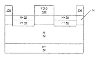
ここで図1を参照して、本発明の一部の実施形態による縦型パワーMOSFETの実施形態を示す断面図について説明する。縦型シリコンカーバイドMOSFETは、一般に、ユニットセル内で複製されることが当業者によって理解されるであろう。こうしたユニットセルは、線100aと100cとの間または線100bと100cと間に示される。例示を容易にするために、2つのユニットセルMOSFETが説明されるが、当業者によって認識されるように、本発明の範囲から逸脱することなく、さらなるユニットセルが、一方向に沿って、または、2つの方向、一般に、直交方向に沿ってMOSFET内に組み込まれてもよい。
Referring now to FIG. 1, a cross-sectional view illustrating an embodiment of a vertical power MOSFET according to some embodiments of the present invention will be described. It will be appreciated by those skilled in the art that vertical silicon carbide MOSFETs are typically replicated within a unit cell. Such unit cells are shown between
図1に示すように、本発明の一部の実施形態によるMOSFETは、n+単結晶シリコンカーバイド基板10、たとえば、4Hシリコンカーバイドを含む。n−シリコンカーバイド層12は、基板10の第1表面10A上に設けられる。本明細書で使用されるように、「p+」または「n+」は、同じまたは別の層または基板の隣接領域または他の領域内に存在する、高いキャリア濃度によって規定される領域を指す。同様に、「p−」または「n−」は、同じまたは別の層または基板の隣接領域または他の領域内に存在する、低いキャリア濃度によって規定される領域を指す。
As shown in FIG. 1, a MOSFET according to some embodiments of the present invention includes an n + single crystal
本発明の一部の実施形態では、n−基板は、デバイスのn−ドリフト層の役をすることができる。本発明のこれらの実施形態では、n+ドレイン領域は、n−基板の第2表面10B上に設けられてもよい。n+ドレイン領域は、本発明の範囲から逸脱することなく、イオン注入またはエピタキシャル成長によって設けられてもよい。
In some embodiments of the present invention, the n - substrate can serve as the n - drift layer of the device. In these embodiments of the present invention, the n + drain region may be provided on the
p型シリコンカーバイド領域14は、n−シリコンカーバイド層12上に設けられ、MOSFETのpウェル領域を提供してもよい。本発明の範囲から逸脱することなく、pウェル領域は、エピタキシャル領域または注入領域であってよいことが理解されるであろう。
The p-type
p+シリコンカーバイドの埋込み領域18は、p型領域14内に同様に設けられるシリコンカーバイドのn+領域20の下でpウェル領域14内に設けられる。n+領域20は、デバイスのソース領域を提供してもよい。n+ソース領域20には、pウェル領域14中を通ってn−シリコンカーバイド層12まで延在する(extend)n型シリコンカーバイド領域21が離間して隣接する。pウェル領域14がエピタキシャル層である本発明の実施形態では、n型シリコンカーバイド領域21は、デバイスの接合型電界効果トランジスタ(JFET)領域と呼ばれてもよいことが理解されるであろう。
A buried
n型シリコンカーバイド領域21は、n型チャネル領域29の一部分を提供してもよい。n型シリコンカーバイド領域21の表面は、それぞれ最大数百オングストロームの好ましくない段差を含む場合があり、好ましくない段差は、デバイスの、オン抵抗の増加および信頼性の低下をもたらす場合がある。さらに、n型シリコンカーバイド領域21とp+シリコンカーバイドの埋込み領域18との間のp型領域31の表面もまた、これらの好ましくない段差を含む場合がある。そのため、図1に示すように、本発明の一部の実施形態によるn−領域19’は、n型シリコンカーバイド領域21およびp型領域31上に設けられ、デバイスのチャネル領域29を形成してもよい。特に、図2Aから図2Jに関して以下でさらに説明されるように、n型エピタキシャル層は、n型シリコンカーバイド領域21、p型領域31、および構造の他の表面上で再成長し、n−領域19’の一部分が、デバイスのn型シリコンカーバイド領域21およびp型領域31上に残るが、n+ソース領域20から除去されるように選択的に除去されてもよい。
The n-type
再成長は、同一譲受人に譲渡された、2003年4月24日に出願された「Silicon Carbide Power Devices With Self−Aligned Source And Well Regions And Well Regions and Methods Of Fabricating Same」という名称の特許文献4、2003年10月30日に出願された「Vertical JFET Limited Silicon Carbide Power Metal−Oxide Semiconductor Field Effect Transistors and Methods of Fabricating Vertical JFET Limited Silicon Carbide Metal−Oxide Semiconductor Field Effect Transistors」という名称の特許文献5、および、2001年6月24日に出願された「Silicon Carbide Power Metal−Oxide Semiconductor Field Effect Transistors Having a Shorting Channel and Methods of Fabricating Silicon Carbide Power Metal−Oxide Semiconductor Field Effect Transistors Having a Shorting Channel」という名称の特許文献6に詳細に説明される。 Re-growth is a patent entitled “Silicon Carbide Power Devices With Self-And-And-Regions And Wells Of Mess 4” filed on April 24, 2003, assigned to the same assignee. , “Vertical JFET Limited Silicon Carbide Power Metal-Oxide Semiconductor Field Effect of Semiconductor Transducers and Methods of Fabricated Semiconductors of the United States, filed Oct. 30, 2003. etal-Oxide Semiconductor Field Effect Transistors "Patent Document 5 entitled, and, filed on June 24, 2001" Silicon Carbide Power Metal-Oxide Semiconductor Field Effect Transistors Having a Shorting Channel and Methods of Fabricating Silicon Carbide Power Metal It is described in detail in Patent Document 6 entitled “Oxide Semiconductor Field Effect Transistors Having a Shorting Channel”.
n型シリコンカーバイド領域21およびp型領域31上でのn−領域19’の存在は、チャネル領域29(n型シリコンカーバイド領域21、p型領域31、およびn−領域19’の残りの部分の組合せ)の表面粗さを低減することができる。換言すれば、n−領域19’は、n型シリコンカーバイド領域21およびp型領域31の表面上の山と谷の一部を充填して、チャネル領域29とゲート絶縁層30(以下で説明する)との間により平滑な界面35を提供してもよい。本発明の一部の実施形態によれば、チャネル領域29は、約1.0Å未満の2乗平均平方根(RMS)表面粗さを有してもよい。こうして、本発明の一部の実施形態によれば、少なくとも約28Åから約1.0Å未満のRMS表面粗さの低減を実現できる。このことについては、図2Aから図3(c)に関して以下でさらに説明される。本発明の一部の実施形態によれば、任意選択の犠牲酸化物層(図示せず)が、チャネル領域29の表面上に設けられ、その後除去されてもよい。犠牲酸化物層は、約100から約1000Å、たとえば、500Åの厚さを有してもよい。犠牲酸化物層の形成および除去は、さらに、チャネル領域29の表面のRMS表面粗さを、約0.70Åに低減することができる。
The presence of the n − region 19 ′ on the n-type
二酸化シリコン(SiO2)などの適した誘電性材料のゲート絶縁層30は、チャネル領域29の上から、n+ソース領域20まで延在する。ゲートコンタクト26は、n型シリコンカーバイド領域21、p型領域31、およびn−領域19’を含むチャネル領域29に対向するゲート層上に設けられる。ソースコンタクト24は、n+ソース領域20間に設けられ、ドレインコンタクト28は、p型領域14に対向する基板10の第2面10B上に設けられる。
A
本発明の実施形態は、図1に示すMOSFET構造に関して説明されるが、本発明の実施形態は、この構成に限定されないことが理解されるであろう。たとえば、本発明の一部の実施形態では、MOSFETは、「Silicon Carbide Devices With Hybrid Well Regions And Methods of Fabricating Silicon Carbide Devices With Hybrid Well Regions」という名称の、2004年6月22日に出願された同一譲受人に譲渡された特許文献7に記載されるハイブリッドウェル構造を含んでもよい。 While embodiments of the present invention will be described with respect to the MOSFET structure shown in FIG. 1, it will be understood that embodiments of the present invention are not limited to this configuration. For example, in some embodiments of the present invention, the MOSFET is “Silicon Carbide Devices With Hybrid Well Regions And Methods of Fabricating Silicon Carbide Devices With Hybrid Year 6” You may include the hybrid well structure described in the patent document 7 assigned to the assignee.
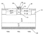
ここで図2Aから図2Jを参照して、本発明の一部の実施形態による、パワーデバイス、たとえばMOSFETの作製における処理工程を説明する。図2Aに示すように、n−エピタキシャル層12が、n+シリコンカーバイド基板10、たとえば、4Hシリコンカーバイド基板上に形成される。n−層12は、約5から約200μmの厚さおよび約1×1014cm−3から1×1017cm−3のキャリア濃度を提供するためのドーピングを有してもよい。本発明の特定の実施形態では、n−層12は、約12μm厚であり、約5×1015cm−3のキャリア濃度を提供するようにドープされる。
Referring now to FIGS. 2A-2J, process steps in the fabrication of a power device, eg, a MOSFET, according to some embodiments of the present invention will be described. As shown in FIG. 2A, an n − epitaxial layer 12 is formed on an n +
p型層14は、n−エピタキシャル層12上に設けられる。先に説明したように、p型層14は、デバイスのpウェル領域を提供してもよい。p型層14は、本発明の範囲から逸脱することなく、エピタキシャル領域または注入領域であってよい。特に、p型層14が注入領域である本発明の実施形態では、p型層14を設けるために、p型シリコンカーバイドドーパントが、n−層12内に注入されてもよい。p型層14がエピタキシャル層である本発明の実施形態では、p型層14は、n−層12上で成長してもよい。p型層14は、約0.5から約3μmの厚さおよび約2×1016cm−3から約5×1017cm−3のキャリア濃度を提供するためのドーピングを有してもよい。本発明の特定の実施形態では、p型層14は、約0.5μm厚であり、約1×1016cm−3のキャリア濃度を提供するようにドープされる。図2Aにさらに示すように、マスク層100は、p型層14上に形成され、デバイスのソース領域20および埋込みp型領域18に相当する開口を形成するようにパターニングされる。
The p-
図2Bおよび図2Cに示すように、埋込みp型領域18およびソース領域20は、ソース領域20のロケーションに相当する開口を有するようマスク層100をパターニングすることによって形成されてもよい。埋込みp型領域18は、パターニングされたマスク100を使用したp型ドーパントのイオン注入によって形成される。埋込みp型領域18は、ドリフト領域、たとえば、n−層12まで延在し、また、一部の実施形態では、n−層12内に延在してもよい。p型ドーパントは、たとえば、アルミニウムまたは他の適したp型ドーパントであってよい。本発明のいくつかの実施形態では、p型領域18は、ほぼ、領域21が形成されてもよい厚さ、たとえば、約0.2μmから約1μmの厚さを有する。本発明の特定の実施形態では、埋込みp型領域18は、p型層14の表面から約0.2μmの深さから約0.7μmの深さまで延在する。さらに、p型領域18は、約1×1017cm−3から約1×1018cm−3のキャリア濃度を提供するためにドープされてもよい。
As shown in FIGS. 2B and 2C, the buried p-
図2Cに示すように、ソース領域20は、パターニングされたマスク100を利用してn型ドーパントをp型層14内に注入することによって形成される。n型注入物のために使用されるn型ドーパントは、たとえば、窒素および/またはリンであってよいが、他のn型ドーパントが、使用されてもよい。n型ソース領域20は、p型層内に約0.2μmから約0.3μmの距離だけ延在してもよい。n型ソース領域20は、良好なオーミックコンタクトの形成を可能にするのに十分なキャリア濃度を提供するようにドープされてもよい。本明細書で使用されるように、「オーミックコンタクト」という用語は、オーミックコンタクトに関連するインピーダンスが、実質的に全ての予想される動作周波数および電流において、実質的に、インピーダンス=V/I(Vはコンタクトの両端の電圧であり、Iは電流である)の関係で与えられる(すなわち、オーミックコンタクトに関連するインピーダンスは、全ての動作周波数において実質的に同じである)コンタクトを指す。本発明の特定の実施形態では、n型ソース領域は、p型層内に約0.2μmの深さまで延在し、少なくとも、約1×1019cm−3から約1×1020cm−3のキャリア濃度を提供するためにドープされる。
As shown in FIG. 2C, the
本発明の実施形態は、p型領域18とソース領域20の両方の注入のために、パターニングされたマスク100内で同じ窓を使用して、本明細書で述べられるが、本発明の一部の実施形態では、注入における失敗を補償するために、異なるサイズの窓が使用されてもよい。
Embodiments of the present invention are described herein using the same window in the patterned
図2Dから図2Eに示すように、マスク100は、除去され、デバイスのn型シリコンカーバイド領域21が、pウェル領域14内に設けられてもよい。n型シリコンカーバイド領域21は、本発明の範囲から逸脱することなく、注入領域またはエピタキシャル領域であってよい。n型シリコンカーバイド領域21が注入領域である本発明の実施形態では、第2マスク層120が、図2Dに示すように、デバイスのn型シリコンカーバイド領域21に相当する開口を有するようにパターニングされてもよい。pウェル領域14がエピタキシャル層である本発明の実施形態では、n型シリコンカーバイド領域21は、デバイスの接合型電界効果トランジスタ(JFET)領域と呼ばれてもよいことが理解されるであろう。
As shown in FIGS. 2D to 2E, the
図2Eに示すように、p型層14を通ってドリフト領域、たとえばn型エピタキシャル層12まで延在するn型シリコンカーバイド領域21を形成するために、n型シリコンカーバイド領域21は、パターニングされたマスク120を利用してp型層14内にn型ドーパントを注入することによって形成されてもよい。どんな適したn型ドーパントが使用されてもよい。本発明の一部の実施形態では、窒素が、n型ドーパントとして使用される。
As shown in FIG. 2E, the n-type
デバイスがターンオンされると、n型領域21は、MOSチャネルから低濃度でドープしたドリフト領域(12)への経路を提供することができ、電子が、ソース領域からドレイン領域へ流れることを可能にする。オフ状態では、このnチャネル領域は、チャネル領域の両側で形成される逆バイアスされたpn接合によって電子が枯渇する場合がある。チャネル領域の両側におけるpn接合は、オフ状態の高い電界からMOS領域をシールドしてもよく、このことが、UMOSFETなどのトレンチデバイスと比較して、高いデバイス信頼性をもたらす可能性がある。
When the device is turned on, the n-
図2Fは、堆積した酸化物および/または他のパッシベーション材料の任意選択のキャップ層140の形成を示す。キャップ層140は、約0.01μmから約1μmの厚さを有してもよい。いずれにしても、キャップ層140が利用されるか否かによらず、n型およびp型注入物を活性化するために、デバイスは、たとえば、5分などの数分の間、約900℃から約1800℃の範囲の、また、一部の実施形態では、約1600℃の高温アニールにさらされてもよい。
FIG. 2F illustrates the formation of an
図2Gに示すように、キャップ層140は、除去され、n−シリコンカーバイドエピタキシャル領域19が、デバイスのチャネル領域29上に形成されてもよい。n−シリコンカーバイドエピタキシャル領域19の深さは、後続の処理工程において、n−領域19の一部分だけが、チャネル領域29から除去されるように制御されてもよい。本発明の一部の実施形態では、n−シリコンカーバイド領域は、約1500Åから約6000Åの厚さ、および、約5×1015cm−3のキャリア濃度を有してもよい。
As shown in FIG. 2G, the
図2Hに示すように、n−領域19の一部分が除去される。n型シリコンカーバイド領域21およびp型領域31上に残るn−領域の部分19’は、デバイスのチャネル領域29(図2I)を画定してもよい。n−領域の残りの部分19’は、約1000から約5000Åの厚さを有してもよい。本発明の一部の実施形態では、n−領域の残りの部分19’は、約1500Åの厚さを有してもよい。チャネル領域29上でのn−領域の残りの部分19’の存在は、n−領域19’とゲート絶縁体30との間の界面35において、チャネル領域29の表面粗さの低減を提供してもよく、このことは、図3に関して以下でさらに説明されるであろう。
As shown in FIG. 2H, a portion of n − region 19 is removed. The
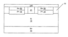
チャネル領域29が、n−領域の残りの部分19’およびn型シリコンカーバイド領域21と埋込みp型領域18との間のpウェルの部分31およびソース領域20によって画定されることが理解されるであろう。相応して、本発明の範囲から逸脱することなく、n−領域19’は、n型シリコンカーバイド領域21と埋込みp型領域18との間のpウェルの部分31およびソース領域20上に残るだけであり、n型シリコンカーバイド領域21上に残らなくてもよい。
It will be understood that the
本発明の一部の実施形態では、チャネル領域29の表面からn−領域19の一部分を除去する化学機械研磨(CMP)プロセスが実施されてもよい。本発明のいくつかの実施形態では、CMPプロセスが、チャネル領域29の表面粗さの深さの約2.0から3.0倍である、n−領域19の一部分を除去してもよい。本発明の範囲から逸脱することなく、従来のどんなCMPプロセスも、本明細書で説明されるCMPプロセスとして使用されてもよいことが理解されるであろう。しかし、本明細書で説明するプロセスは、n−領域19全体を除去しない。通常、注入領域は、数百オングストロームの厚さを有し、従来のCMPプロセスは、所望の結果を得るために、CMPプロセス中に数ミクロンの膜を除去する。しかし、当業者によって理解されるように、図2Gの構造からの数ミクロンの膜の除去は、注入領域の全てを除去し、デバイスを非機能的にさせる。
In some embodiments of the present invention, a chemical mechanical polishing (CMP) process may be performed that removes a portion of the n − region 19 from the surface of the
相応して、本発明の一部の実施形態は、n−領域19の一部分を除去するCMPプロセスを使用し、チャネル領域29上にn−領域の一部分19’を残したままにする。たとえば、本発明の一部の実施形態では、CMPプロセスは、約3時間未満、たとえば、約半時間から約1時間の間実施されてもよい。換言すれば、CMPプロセス後に、約1000から約5000Åのn−領域19が、デバイスのチャネル領域29上に残ってもよい。こうして、n−領域の残りの部分が、約1000から約5000Åであってよい。n型シリコンカーバイド領域21およびpウェル領域31上のn−領域の残りの部分19’は、チャネル領域29の一部になる。すなわち、n−領域の残りの部分19’は、n型シリコンカーバイド領域21およびpウェル領域31の表面上の山と谷を充填してもよい。図2Hにさらに示すように、マスク130が、n−領域の残りの部分19’上に設けられ、n−領域19’が、マスク130に従ってパターニングされ、図2Iに示すように、ソース領域20上のn−領域の部分19’を除去する。先に説明したように、本発明の一部の実施形態では、n−領域19’は、n型シリコンカーバイド領域21とソース領域20との間のpウェル領域31および埋込みp型領域18上に残るだけであってよい。
Correspondingly, some embodiments of the present invention, n - using a CMP process to remove a portion of the
先に説明したように、n型領域21およびpウェル領域31上にn−領域19’を設けることは、n−領域19’とゲート絶縁体30との間の表面粗さの低減を提供してもよい。たとえば、図3(a)に示すように、n型シリコンカーバイド領域21およびpウェル領域31の表面は、注入領域を活性化するアニール後に、多くの山と谷を有する場合がある。これらの山と谷(数百オングストローム)は、デバイスの最適状態に及ばない性能をもたらす場合がある。本発明の一部の実施形態に従って、n型シリコンカーバイド領域21およびpウェル領域31上にn−領域19を形成し、n型シリコンカーバイド領域21およびpウェル領域31からn−領域の一部分を除去した後、図3(b)に示すように、n−領域の残りの部分19’の存在によって、多くの山と谷が除去されてもよい。特に、チャネル領域29の2乗平均平方根(RMS)表面粗さは、本発明の一部の実施形態に従って、図3(a)の少なくとも約28Åから図3(b)の約1.0Å未満まで低減されてもよい。さらに、本発明の一部の実施形態では、任意選択の犠牲酸化物層(図示せず)が、チャネル領域29の表面上に形成され、除去されてもよい。犠牲酸化物層の形成および除去は、さらに、図3(c)に示すようにRMS表面粗さを約0.70Åまで低減させてもよい。
As described above, providing n − region 19 ′ on
図2Iに示すように、絶縁材料の層30は、ゲート絶縁材料を設けるためにデバイス上に堆積されてもよい。本発明の一部の実施形態では、絶縁材料は、「Method of N2O annealing an oxide layer on a silicon carbide layer」という名称の特許文献8、「Method of N2O growth of an oxide layer on a silicon carbide layer」という名称の特許文献9、および/または、「Method of fabricating an oxide layer on a silicon carbide layer utilizing an anneal in a hydrogen environment」という名称の特許文献10に記載されるように形成されてもよい。本発明のいくつかの実施形態では、絶縁材料は、非特許文献4に記載されるように形成されてもよい。図2Iにさらに示すように、ゲートコンタクト26は、ゲート絶縁材料30上に金属コンタクトを形成することによって形成されてもよい。適したゲートコンタクト材料は、アルミニウム、ポリシリコン、およびモリブデンを含むが、それらに限定されない。さらに、当業者によって認識されるように、多層ゲートコンタクトが使用されてもよい。
As shown in FIG. 2I, a
図2Jに示すように、コンタクトホールが、絶縁材料30’内に形成されてもよく、また、ソースコンタクト24を提供するために、オーミックコンタクトが、コンタクトホール内に形成されてもよい。同様に、オーミックコンタクト28は、基板10上に形成されてもよい。適したオーミックコンタクト材料は、ニッケル、チタン合金、およびアルミニウムを含むが、それらに限定されない。堆積した金属コンタクトは、その後、約500℃から約1200℃の範囲の高温でアニールされてもよい。たとえば、デバイスの接続を容易にするために、オーバレイ金属もまた、コンタクト上に堆積されてもよい。
As shown in FIG. 2J, a contact hole may be formed in the insulating
図2Aから図2Jの工程の順序が変更されてもよいことが当業者によって理解されるであろう。そのため、たとえば、n型シリコンカーバイド領域21は、本発明の範囲から逸脱することなく、n+領域20を形成する前に形成されてもよい。同様に、埋込みp+領域18は、n+領域20またはn型シリコンカーバイド領域21の形成の前か後のいずれかで形成されてもよい。同様に、コンタクト24が、たとえば、金属層を堆積しパターニングすることによって形成され、次に、絶縁層30’が設けられ、絶縁層内の開口が、コンタクト24に対して形成されてもよい。相応して、本発明は、明細書に述べる正確な動作シーケンスに限定されるものとして解釈されるべきではなく、本開示に照らして当業者に明らかになると思われる他の作製シーケンスを包含することが意図される。
It will be appreciated by those skilled in the art that the order of the steps of FIGS. 2A through 2J may be changed. Thus, for example, n-type
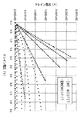
ここで図4を参照して、従来のデバイスと本発明の一部の実施形態による方法を使用して作製されたデバイスについての、ドレイン電圧(V)対ドレイン電流(A)の比較を示すチャートが説明される。図4に示すように、本発明の一部の実施形態に従って作製されたMOSFETのドレイン電流は、相当するドレイン電圧において、従来のMOSFETより大きい。 Referring now to FIG. 4, a chart showing a comparison of drain voltage (V) versus drain current (A) for a conventional device and a device made using the method according to some embodiments of the present invention. Is explained. As shown in FIG. 4, the drain current of a MOSFET fabricated according to some embodiments of the present invention is greater than a conventional MOSFET at the corresponding drain voltage.
図面および明細書において、本発明の典型的な好ましい実施形態が開示されており、特定の用語が使用されるが、特定の用語は、制限するためでなく、一般的でかつ記述的な意味でだけ使用されており、本発明の範囲は、添付特許請求項において述べられる。 In the drawings and specification, there have been disclosed exemplary preferred embodiments of the invention and specific terminology is used, but the specific terms are not meant to be limiting, but in a general and descriptive sense. The scope of the present invention is set forth in the appended claims.
Claims (15)
シリコンカーバイド基板上にn−シリコンカーバイド層を形成するステップ、
前記n−シリコンカーバイド層上にp型シリコンカーバイドウェル領域を形成するために、前記n−シリコンカーバイド層内にp型ドーパントを注入するステップ、または、前記n−シリコンカーバイド層上にp型エピタキシャル層を形成するステップ、
前記p型シリコンカーバイドウェル領域内にp+シリコンカーバイドの埋込み領域を形成するために、前記p型シリコンカーバイドウェル領域内にp型ドーパントを注入するステップ、
n型ドーパントをp+シリコンカーバイドの埋込み領域上のp型シリコンカーバイドウェルにインプラントして、p+シリコンカーバイドの埋込み領域上に、シリコンカーバイドのn+領域を形成するステップであって、パワーデバイスのチャネル領域はp+の埋込み領域とシリコンカーバイドのn+領域に隣接し、
前記チャネル領域上に、再成長プロセスでn−シリコンカーバイドエピタキシャル領域を形成するステップ、および、
前記チャネル領域から前記n−領域の表面の一部分を化学機械研磨(CMP)プロセスで除去するステップであって、それにより、前記n−領域の一部分が、前記チャネル領域上に残って、前記チャネル領域の表面粗さを低減する、ことを特徴とする方法。A method of forming a silicon carbide power device comprising:
Forming an n - silicon carbide layer on a silicon carbide substrate;
Wherein the n - to form a p-type silicon carbide well region on the silicon carbide layer, the n - step implanting p-type dopant into the silicon carbide layer or the n - p-type epitaxial layer on a silicon carbide layer Forming steps,
Implanting a p-type dopant into the p-type silicon carbide well region to form a buried region of p + silicon carbide in the p-type silicon carbide well region;
The n-type dopant implanted in the p-type silicon carbide well on the buried region of p + silicon carbide, on the buried region of p + silicon carbide, comprising the steps of forming a n + region of the silicon carbide, the power device The channel region is adjacent to the p + buried region and the silicon carbide n + region,
Forming an n - silicon carbide epitaxial region on the channel region by a regrowth process; and
A portion of the surface area comprising the steps of removing by chemical mechanical polishing (CMP) process, whereby the n - - the n from the channel region portion of the region, remains in the channel region, the channel region Reducing the surface roughness of the substrate.
前記チャネル領域上の前記n−領域の残りの部分上に、100から1000Åの厚さを有する犠牲酸化物層を形成するステップ、および、
前記犠牲酸化物層を除去するステップを続いて伴い、前記RMS表円面粗さは、前記犠牲酸化物層の形成および1.0Åから0.70Åまでの前記犠牲酸化物層の除去によってさらに低減されることを特徴とする請求項5に記載の方法。Forming the sacrificial oxide layer having a thickness of 100 to 1000 on the remaining portion of the n − region on the channel region; and
Following the step of removing the sacrificial oxide layer, the RMS surface roughness is further reduced by forming the sacrificial oxide layer and removing the sacrificial oxide layer from 1.0 to 0.70 mm. 6. The method of claim 5, wherein:
Applications Claiming Priority (3)
| Application Number | Priority Date | Filing Date | Title |
|---|---|---|---|
| US11/136,057 | 2005-05-24 | ||
| US11/136,057 US7528040B2 (en) | 2005-05-24 | 2005-05-24 | Methods of fabricating silicon carbide devices having smooth channels |
| PCT/US2006/009493 WO2006127093A2 (en) | 2005-05-24 | 2006-03-16 | Methods of fabricating silicon carbide devices having a smooth surface of the channel regions |
Related Child Applications (1)
| Application Number | Title | Priority Date | Filing Date |
|---|---|---|---|
| JP2012111459A Division JP6008571B2 (en) | 2005-05-24 | 2012-05-15 | Method for fabricating a silicon carbide device having a smooth surface in a channel region |
Publications (2)
| Publication Number | Publication Date |
|---|---|
| JP2008543048A JP2008543048A (en) | 2008-11-27 |
| JP5199072B2 true JP5199072B2 (en) | 2013-05-15 |
Family
ID=36753949
Family Applications (2)
| Application Number | Title | Priority Date | Filing Date |
|---|---|---|---|
| JP2008513462A Active JP5199072B2 (en) | 2005-05-24 | 2006-03-16 | Method for fabricating a silicon carbide device having a smooth surface in a channel region |
| JP2012111459A Active JP6008571B2 (en) | 2005-05-24 | 2012-05-15 | Method for fabricating a silicon carbide device having a smooth surface in a channel region |
Family Applications After (1)
| Application Number | Title | Priority Date | Filing Date |
|---|---|---|---|
| JP2012111459A Active JP6008571B2 (en) | 2005-05-24 | 2012-05-15 | Method for fabricating a silicon carbide device having a smooth surface in a channel region |
Country Status (5)
| Country | Link |
|---|---|
| US (4) | US7528040B2 (en) |
| EP (2) | EP1883951B1 (en) |
| JP (2) | JP5199072B2 (en) |
| TW (2) | TWI404131B (en) |
| WO (1) | WO2006127093A2 (en) |
Families Citing this family (41)
| Publication number | Priority date | Publication date | Assignee | Title |
|---|---|---|---|---|
| US7569900B2 (en) * | 2004-11-16 | 2009-08-04 | Kabushiki Kaisha Toshiba | Silicon carbide high breakdown voltage semiconductor device |
| US8367510B2 (en) * | 2005-09-14 | 2013-02-05 | Central Research Institute Of Electric Power Industry | Process for producing silicon carbide semiconductor device |
| EP2674966B1 (en) * | 2006-06-29 | 2019-10-23 | Cree, Inc. | Silicon carbide switching devices including P-type channels |
| US8272781B2 (en) * | 2006-08-01 | 2012-09-25 | Intel Corporation | Dynamic power control of a memory device thermal sensor |
| US8432012B2 (en) | 2006-08-01 | 2013-04-30 | Cree, Inc. | Semiconductor devices including schottky diodes having overlapping doped regions and methods of fabricating same |
| US7728402B2 (en) * | 2006-08-01 | 2010-06-01 | Cree, Inc. | Semiconductor devices including schottky diodes with controlled breakdown |
| WO2008020911A2 (en) * | 2006-08-17 | 2008-02-21 | Cree, Inc. | High power insulated gate bipolar transistors |
| JP5071763B2 (en) * | 2006-10-16 | 2012-11-14 | 独立行政法人産業技術総合研究所 | Silicon carbide semiconductor device and manufacturing method thereof |
| US7781312B2 (en) * | 2006-12-13 | 2010-08-24 | General Electric Company | Silicon carbide devices and method of making |
| US8835987B2 (en) * | 2007-02-27 | 2014-09-16 | Cree, Inc. | Insulated gate bipolar transistors including current suppressing layers |
| JP4700045B2 (en) * | 2007-11-13 | 2011-06-15 | Okiセミコンダクタ株式会社 | Manufacturing method of semiconductor device |
| US7795691B2 (en) * | 2008-01-25 | 2010-09-14 | Cree, Inc. | Semiconductor transistor with P type re-grown channel layer |
| TWI364798B (en) * | 2008-03-21 | 2012-05-21 | Vanguard Int Semiconduct Corp | Semiconductor device and fabrication method thereof |
| US8232558B2 (en) | 2008-05-21 | 2012-07-31 | Cree, Inc. | Junction barrier Schottky diodes with current surge capability |
| US8294507B2 (en) | 2009-05-08 | 2012-10-23 | Cree, Inc. | Wide bandgap bipolar turn-off thyristor having non-negative temperature coefficient and related control circuits |
| US8629509B2 (en) * | 2009-06-02 | 2014-01-14 | Cree, Inc. | High voltage insulated gate bipolar transistors with minority carrier diverter |
| US8193848B2 (en) | 2009-06-02 | 2012-06-05 | Cree, Inc. | Power switching devices having controllable surge current capabilities |
| US8541787B2 (en) * | 2009-07-15 | 2013-09-24 | Cree, Inc. | High breakdown voltage wide band-gap MOS-gated bipolar junction transistors with avalanche capability |
| JP5474068B2 (en) * | 2009-07-24 | 2014-04-16 | 三菱電機株式会社 | Method for manufacturing silicon carbide semiconductor device |
| US8354690B2 (en) | 2009-08-31 | 2013-01-15 | Cree, Inc. | Solid-state pinch off thyristor circuits |
| US9117739B2 (en) | 2010-03-08 | 2015-08-25 | Cree, Inc. | Semiconductor devices with heterojunction barrier regions and methods of fabricating same |
| US8415671B2 (en) | 2010-04-16 | 2013-04-09 | Cree, Inc. | Wide band-gap MOSFETs having a heterojunction under gate trenches thereof and related methods of forming such devices |
| US9142662B2 (en) | 2011-05-06 | 2015-09-22 | Cree, Inc. | Field effect transistor devices with low source resistance |
| US9673283B2 (en) | 2011-05-06 | 2017-06-06 | Cree, Inc. | Power module for supporting high current densities |
| US9029945B2 (en) | 2011-05-06 | 2015-05-12 | Cree, Inc. | Field effect transistor devices with low source resistance |
| US8618582B2 (en) | 2011-09-11 | 2013-12-31 | Cree, Inc. | Edge termination structure employing recesses for edge termination elements |
| US8664665B2 (en) | 2011-09-11 | 2014-03-04 | Cree, Inc. | Schottky diode employing recesses for elements of junction barrier array |
| US8680587B2 (en) | 2011-09-11 | 2014-03-25 | Cree, Inc. | Schottky diode |
| US9640617B2 (en) | 2011-09-11 | 2017-05-02 | Cree, Inc. | High performance power module |
| US9373617B2 (en) | 2011-09-11 | 2016-06-21 | Cree, Inc. | High current, low switching loss SiC power module |
| DE102013010187A1 (en) | 2012-06-27 | 2014-01-02 | Fairchild Semiconductor Corp. | Schottky barrier device with locally planarized surface and associated semiconductor product |
| JP5961563B2 (en) * | 2013-01-25 | 2016-08-02 | 株式会社豊田中央研究所 | Manufacturing method of semiconductor device |
| JP2015041644A (en) * | 2013-08-20 | 2015-03-02 | 富士電機株式会社 | Method of manufacturing mos type semiconductor device |
| JP6347188B2 (en) * | 2014-09-08 | 2018-06-27 | 富士電機株式会社 | Silicon carbide semiconductor device manufacturing method and silicon carbide semiconductor device |
| US9685550B2 (en) * | 2014-12-26 | 2017-06-20 | Fairchild Semiconductor Corporation | Silicon carbide (SiC) device with improved gate dielectric shielding |
| JP6351874B2 (en) * | 2015-12-02 | 2018-07-04 | 三菱電機株式会社 | Silicon carbide epitaxial substrate and silicon carbide semiconductor device |
| JP6237845B1 (en) * | 2016-08-24 | 2017-11-29 | 富士電機株式会社 | Vertical MOSFET and manufacturing method of vertical MOSFET |
| EP3358626B1 (en) * | 2017-02-02 | 2022-07-20 | Nxp B.V. | Method of making a semiconductor switch device |
| CN107331621A (en) * | 2017-07-14 | 2017-11-07 | 欧阳慧琳 | A kind of vertical bilateral diffusion field-effect tranisistor and preparation method thereof |
| CN110718452A (en) | 2018-07-12 | 2020-01-21 | 创能动力科技有限公司 | Silicon carbide device and method for manufacturing same |
| CN113381599B (en) * | 2021-06-29 | 2022-11-29 | 哈尔滨工业大学 | Parallel SiC MOSFET safety working domain calculation method |
Family Cites Families (109)
| Publication number | Priority date | Publication date | Assignee | Title |
|---|---|---|---|---|
| US3629011A (en) | 1967-09-11 | 1971-12-21 | Matsushita Electric Ind Co Ltd | Method for diffusing an impurity substance into silicon carbide |
| US4466172A (en) | 1979-01-08 | 1984-08-21 | American Microsystems, Inc. | Method for fabricating MOS device with self-aligned contacts |
| JPS58175872A (en) * | 1982-04-08 | 1983-10-15 | Toshiba Corp | Insulated gate field effect transistor |
| US4779126A (en) | 1983-11-25 | 1988-10-18 | International Rectifier Corporation | Optically triggered lateral thyristor with auxiliary region |
| JPS63132481A (en) * | 1986-11-22 | 1988-06-04 | Toshiba Corp | Manufacture of field effect transistor |
| US4811065A (en) | 1987-06-11 | 1989-03-07 | Siliconix Incorporated | Power DMOS transistor with high speed body diode |
| JPH01117363A (en) | 1987-10-30 | 1989-05-10 | Nec Corp | Vertical insulated gate field effect transistor |
| US5111253A (en) | 1989-05-09 | 1992-05-05 | General Electric Company | Multicellular FET having a Schottky diode merged therewith |
| JPH0766971B2 (en) | 1989-06-07 | 1995-07-19 | シャープ株式会社 | Silicon carbide semiconductor device |
| JPH0334466A (en) | 1989-06-30 | 1991-02-14 | Nippon Telegr & Teleph Corp <Ntt> | Vertical-type double diffused mosfet |
| JPH03157974A (en) | 1989-11-15 | 1991-07-05 | Nec Corp | Vertical type field effect transistor |
| JP2542448B2 (en) | 1990-05-24 | 1996-10-09 | シャープ株式会社 | Field effect transistor and method of manufacturing the same |
| US5270554A (en) | 1991-06-14 | 1993-12-14 | Cree Research, Inc. | High power high frequency metal-semiconductor field-effect transistor formed in silicon carbide |
| US5242841A (en) | 1992-03-25 | 1993-09-07 | Texas Instruments Incorporated | Method of making LDMOS transistor with self-aligned source/backgate and photo-aligned gate |
| US5459107A (en) | 1992-06-05 | 1995-10-17 | Cree Research, Inc. | Method of obtaining high quality silicon dioxide passivation on silicon carbide and resulting passivated structures |
| US6344663B1 (en) | 1992-06-05 | 2002-02-05 | Cree, Inc. | Silicon carbide CMOS devices |
| US5629531A (en) | 1992-06-05 | 1997-05-13 | Cree Research, Inc. | Method of obtaining high quality silicon dioxide passivation on silicon carbide and resulting passivated structures |
| US5726463A (en) | 1992-08-07 | 1998-03-10 | General Electric Company | Silicon carbide MOSFET having self-aligned gate structure |
| JP3146694B2 (en) | 1992-11-12 | 2001-03-19 | 富士電機株式会社 | Silicon carbide MOSFET and method of manufacturing silicon carbide MOSFET |
| US5506421A (en) | 1992-11-24 | 1996-04-09 | Cree Research, Inc. | Power MOSFET in silicon carbide |
| JPH0799312A (en) | 1993-02-22 | 1995-04-11 | Texas Instr Inc <Ti> | Semiconductor device and its manufacturing process |
| US5539217A (en) | 1993-08-09 | 1996-07-23 | Cree Research, Inc. | Silicon carbide thyristor |
| US6162665A (en) | 1993-10-15 | 2000-12-19 | Ixys Corporation | High voltage transistors and thyristors |
| US5510630A (en) | 1993-10-18 | 1996-04-23 | Westinghouse Electric Corporation | Non-volatile random access memory cell constructed of silicon carbide |
| JP3210510B2 (en) | 1993-12-17 | 2001-09-17 | 株式会社東芝 | Method for manufacturing semiconductor device |
| US5396085A (en) | 1993-12-28 | 1995-03-07 | North Carolina State University | Silicon carbide switching device with rectifying-gate |
| US5385855A (en) | 1994-02-24 | 1995-01-31 | General Electric Company | Fabrication of silicon carbide integrated circuits |
| JPH08213607A (en) | 1995-02-08 | 1996-08-20 | Ngk Insulators Ltd | Semiconductor device and its manufacturing method |
| US5510281A (en) | 1995-03-20 | 1996-04-23 | General Electric Company | Method of fabricating a self-aligned DMOS transistor device using SiC and spacers |
| JP3521246B2 (en) | 1995-03-27 | 2004-04-19 | 沖電気工業株式会社 | Field effect transistor and method of manufacturing the same |
| SE9501310D0 (en) | 1995-04-10 | 1995-04-10 | Abb Research Ltd | A method for introducing an impurity dopant into SiC, a semiconductor device formed by the method and using a highly doped amorphous layer as a source for dopant diffusion into SiC |
| US5734180A (en) | 1995-06-02 | 1998-03-31 | Texas Instruments Incorporated | High-performance high-voltage device structures |
| US5967795A (en) | 1995-08-30 | 1999-10-19 | Asea Brown Boveri Ab | SiC semiconductor device comprising a pn junction with a voltage absorbing edge |
| JP3385938B2 (en) * | 1997-03-05 | 2003-03-10 | 株式会社デンソー | Silicon carbide semiconductor device and method of manufacturing the same |
| JPH11261061A (en) | 1998-03-11 | 1999-09-24 | Denso Corp | Silicon carbide semiconductor device and its manufacture |
| DE19636302C2 (en) | 1995-09-06 | 1998-08-20 | Denso Corp | Silicon carbide semiconductor device and manufacturing method |
| US6573534B1 (en) * | 1995-09-06 | 2003-06-03 | Denso Corporation | Silicon carbide semiconductor device |
| US5972801A (en) | 1995-11-08 | 1999-10-26 | Cree Research, Inc. | Process for reducing defects in oxide layers on silicon carbide |
| US6133587A (en) | 1996-01-23 | 2000-10-17 | Denso Corporation | Silicon carbide semiconductor device and process for manufacturing same |
| JPH09205202A (en) | 1996-01-26 | 1997-08-05 | Matsushita Electric Works Ltd | Semiconductor device |
| US5663580A (en) | 1996-03-15 | 1997-09-02 | Abb Research Ltd. | Optically triggered semiconductor device |
| SE9601174D0 (en) | 1996-03-27 | 1996-03-27 | Abb Research Ltd | A method for producing a semiconductor device having a semiconductor layer of SiC and such a device |
| TW350621U (en) | 1996-04-15 | 1999-01-11 | Rohm Co Ltd | Image sensor chip, method for manufacturing the same, and image sensor |
| US5763905A (en) | 1996-07-09 | 1998-06-09 | Abb Research Ltd. | Semiconductor device having a passivation layer |
| SE9602745D0 (en) | 1996-07-11 | 1996-07-11 | Abb Research Ltd | A method for producing a channel region layer in a SiC layer for a voltage controlled semiconductor device |
| US6002159A (en) | 1996-07-16 | 1999-12-14 | Abb Research Ltd. | SiC semiconductor device comprising a pn junction with a voltage absorbing edge |
| US5917203A (en) | 1996-07-29 | 1999-06-29 | Motorola, Inc. | Lateral gate vertical drift region transistor |
| US5837572A (en) | 1997-01-10 | 1998-11-17 | Advanced Micro Devices, Inc. | CMOS integrated circuit formed by using removable spacers to produce asymmetrical NMOS junctions before asymmetrical PMOS junctions for optimizing thermal diffusivity of dopants implanted therein |
| US6180958B1 (en) | 1997-02-07 | 2001-01-30 | James Albert Cooper, Jr. | Structure for increasing the maximum voltage of silicon carbide power transistors |
| JP3206727B2 (en) | 1997-02-20 | 2001-09-10 | 富士電機株式会社 | Silicon carbide vertical MOSFET and method of manufacturing the same |
| DE19809554B4 (en) | 1997-03-05 | 2008-04-03 | Denso Corp., Kariya | silicon carbide semiconductor device |
| US5877041A (en) | 1997-06-30 | 1999-03-02 | Harris Corporation | Self-aligned power field effect transistor in silicon carbide |
| DE19832329A1 (en) | 1997-07-31 | 1999-02-04 | Siemens Ag | Silicon carbide semiconductor structure manufacturing method |
| US5976801A (en) * | 1997-08-08 | 1999-11-02 | Incyte Pharamceuticals, Inc. | Human reticulocalbin isoforms |
| JP3180895B2 (en) | 1997-08-18 | 2001-06-25 | 富士電機株式会社 | Method for manufacturing silicon carbide semiconductor device |
| EP1010204A1 (en) | 1997-08-20 | 2000-06-21 | Siemens Aktiengesellschaft | Semiconductor structure comprising an alpha silicon carbide zone, and use of said semiconductor structure |
| US6239463B1 (en) | 1997-08-28 | 2001-05-29 | Siliconix Incorporated | Low resistance power MOSFET or other device containing silicon-germanium layer |
| SE9704150D0 (en) | 1997-11-13 | 1997-11-13 | Abb Research Ltd | Semiconductor device of SiC with insulating layer a refractory metal nitride layer |
| JPH11191559A (en) | 1997-12-26 | 1999-07-13 | Matsushita Electric Works Ltd | Manufacture of mosfet |
| JPH11251592A (en) | 1998-01-05 | 1999-09-07 | Denso Corp | Carbon silicon semiconductor device |
| JP3216804B2 (en) | 1998-01-06 | 2001-10-09 | 富士電機株式会社 | Manufacturing method of silicon carbide vertical FET and silicon carbide vertical FET |
| JPH11266017A (en) | 1998-01-14 | 1999-09-28 | Denso Corp | Silicon carbide semiconductor device and manufacture thereof |
| JPH11238742A (en) | 1998-02-23 | 1999-08-31 | Denso Corp | Manufacture of silicon carbide semiconductor device |
| JP3893725B2 (en) | 1998-03-25 | 2007-03-14 | 株式会社デンソー | Method for manufacturing silicon carbide semiconductor device |
| US6100169A (en) | 1998-06-08 | 2000-08-08 | Cree, Inc. | Methods of fabricating silicon carbide power devices by controlled annealing |
| US6107142A (en) | 1998-06-08 | 2000-08-22 | Cree Research, Inc. | Self-aligned methods of fabricating silicon carbide power devices by implantation and lateral diffusion |
| JP4123636B2 (en) | 1998-06-22 | 2008-07-23 | 株式会社デンソー | Silicon carbide semiconductor device and manufacturing method thereof |
| JP3959856B2 (en) | 1998-07-31 | 2007-08-15 | 株式会社デンソー | Silicon carbide semiconductor device and manufacturing method thereof |
| US6221700B1 (en) | 1998-07-31 | 2001-04-24 | Denso Corporation | Method of manufacturing silicon carbide semiconductor device with high activation rate of impurities |
| JP2000106371A (en) | 1998-07-31 | 2000-04-11 | Denso Corp | Fabrication of silicon carbide semiconductor device |
| US6246076B1 (en) | 1998-08-28 | 2001-06-12 | Cree, Inc. | Layered dielectric on silicon carbide semiconductor structures |
| JP4186337B2 (en) | 1998-09-30 | 2008-11-26 | 株式会社デンソー | Silicon carbide semiconductor device and manufacturing method thereof |
| US6228720B1 (en) | 1999-02-23 | 2001-05-08 | Matsushita Electric Industrial Co., Ltd. | Method for making insulated-gate semiconductor element |
| US6399996B1 (en) | 1999-04-01 | 2002-06-04 | Apd Semiconductor, Inc. | Schottky diode having increased active surface area and method of fabrication |
| US6420225B1 (en) | 1999-04-01 | 2002-07-16 | Apd Semiconductor, Inc. | Method of fabricating power rectifier device |
| US6448160B1 (en) | 1999-04-01 | 2002-09-10 | Apd Semiconductor, Inc. | Method of fabricating power rectifier device to vary operating parameters and resulting device |
| US6238967B1 (en) | 1999-04-12 | 2001-05-29 | Motorola, Inc. | Method of forming embedded DRAM structure |
| US6137139A (en) | 1999-06-03 | 2000-10-24 | Intersil Corporation | Low voltage dual-well MOS device having high ruggedness, low on-resistance, and improved body diode reverse recovery |
| JP4192353B2 (en) | 1999-09-21 | 2008-12-10 | 株式会社デンソー | Silicon carbide semiconductor device and manufacturing method thereof |
| US6303508B1 (en) | 1999-12-16 | 2001-10-16 | Philips Electronics North America Corporation | Superior silicon carbide integrated circuits and method of fabricating |
| US6429041B1 (en) | 2000-07-13 | 2002-08-06 | Cree, Inc. | Methods of fabricating silicon carbide inversion channel devices without the need to utilize P-type implantation |
| DE10036208B4 (en) | 2000-07-25 | 2007-04-19 | Siced Electronics Development Gmbh & Co. Kg | Semiconductor structure with buried island area and contact area |
| JP2003158075A (en) * | 2001-08-23 | 2003-05-30 | Sumitomo Mitsubishi Silicon Corp | Method for manufacturing semiconductor substrate, method for manufacturing field effect transistor, semiconductor substrate and field effect transistor |
| US6610366B2 (en) | 2000-10-03 | 2003-08-26 | Cree, Inc. | Method of N2O annealing an oxide layer on a silicon carbide layer |
| US6767843B2 (en) | 2000-10-03 | 2004-07-27 | Cree, Inc. | Method of N2O growth of an oxide layer on a silicon carbide layer |
| US6956238B2 (en) | 2000-10-03 | 2005-10-18 | Cree, Inc. | Silicon carbide power metal-oxide semiconductor field effect transistors having a shorting channel and methods of fabricating silicon carbide metal-oxide semiconductor field effect transistors having a shorting channel |
| US7067176B2 (en) | 2000-10-03 | 2006-06-27 | Cree, Inc. | Method of fabricating an oxide layer on a silicon carbide layer utilizing an anneal in a hydrogen environment |
| US6593620B1 (en) | 2000-10-06 | 2003-07-15 | General Semiconductor, Inc. | Trench DMOS transistor with embedded trench schottky rectifier |
| US6958508B2 (en) | 2000-10-17 | 2005-10-25 | Matsushita Electric Industrial Co., Ltd. | Ferroelectric memory having ferroelectric capacitor insulative film |
| US7126169B2 (en) | 2000-10-23 | 2006-10-24 | Matsushita Electric Industrial Co., Ltd. | Semiconductor element |
| JP3881840B2 (en) | 2000-11-14 | 2007-02-14 | 独立行政法人産業技術総合研究所 | Semiconductor device |
| JP4792645B2 (en) * | 2001-03-12 | 2011-10-12 | 株式会社デンソー | Method for manufacturing silicon carbide semiconductor device |
| DE10214150B4 (en) | 2001-03-30 | 2009-06-18 | Denso Corporation, Kariya | Silicon carbide semiconductor device and method of manufacturing the same |
| CN1520616A (en) | 2001-04-11 | 2004-08-11 | ��˹�������뵼�幫˾ | Power semiconductor devices having laterally extending base shielding regions that inhibit base reach through and methodds of forming same |
| JP3908128B2 (en) | 2001-09-07 | 2007-04-25 | 株式会社半導体エネルギー研究所 | Method for manufacturing semiconductor device |
| EP1306890A2 (en) | 2001-10-25 | 2003-05-02 | Matsushita Electric Industrial Co., Ltd. | Semiconductor substrate and device comprising SiC and method for fabricating the same |
| JP2003234301A (en) * | 2001-10-25 | 2003-08-22 | Matsushita Electric Ind Co Ltd | Semiconductor substrate, semiconductor element and method for manufacturing the same |
| SE520968C2 (en) | 2001-10-29 | 2003-09-16 | Okmetic Oyj | High-resistance monocrystalline silicon carbide and its method of preparation |
| US7221010B2 (en) * | 2002-12-20 | 2007-05-22 | Cree, Inc. | Vertical JFET limited silicon carbide power metal-oxide semiconductor field effect transistors |
| US7074643B2 (en) | 2003-04-24 | 2006-07-11 | Cree, Inc. | Silicon carbide power devices with self-aligned source and well regions and methods of fabricating same |
| ATE335872T1 (en) | 2003-04-24 | 2006-09-15 | Norstel Ab | DEVICE AND METHOD FOR PRODUCING SINGLE CRYSTALS BY VAPOR PHASE DEPOSITION |
| US6979863B2 (en) | 2003-04-24 | 2005-12-27 | Cree, Inc. | Silicon carbide MOSFETs with integrated antiparallel junction barrier Schottky free wheeling diodes and methods of fabricating the same |
| US7247513B2 (en) | 2003-05-08 | 2007-07-24 | Caracal, Inc. | Dissociation of silicon clusters in a gas phase during chemical vapor deposition homo-epitaxial growth of silicon carbide |
| JP3784393B2 (en) * | 2003-07-02 | 2006-06-07 | 松下電器産業株式会社 | Semiconductor device and manufacturing method thereof |
| US7473929B2 (en) | 2003-07-02 | 2009-01-06 | Panasonic Corporation | Semiconductor device and method for fabricating the same |
| FR2857895B1 (en) * | 2003-07-23 | 2007-01-26 | Soitec Silicon On Insulator | PROCESS FOR PREPARING EPIREADY SURFACE ON SIN THIN FILMS |
| JP2005116896A (en) * | 2003-10-09 | 2005-04-28 | Matsushita Electric Ind Co Ltd | Semiconductor device and its manufacturing method |
| US7118970B2 (en) | 2004-06-22 | 2006-10-10 | Cree, Inc. | Methods of fabricating silicon carbide devices with hybrid well regions |
| JP4500928B2 (en) | 2004-10-25 | 2010-07-14 | アルプス電気株式会社 | Mold manufacturing method |
-
2005
- 2005-05-24 US US11/136,057 patent/US7528040B2/en active Active
-
2006
- 2006-03-16 JP JP2008513462A patent/JP5199072B2/en active Active
- 2006-03-16 TW TW095109031A patent/TWI404131B/en active
- 2006-03-16 EP EP06738542.7A patent/EP1883951B1/en active Active
- 2006-03-16 WO PCT/US2006/009493 patent/WO2006127093A2/en active Application Filing
- 2006-03-16 EP EP10196317.1A patent/EP2325869B1/en active Active
- 2006-03-16 TW TW101149631A patent/TWI545640B/en active
-
2009
- 2009-04-16 US US12/424,960 patent/US8188483B2/en active Active
-
2012
- 2012-05-14 US US13/470,600 patent/US8859366B2/en active Active
- 2012-05-15 JP JP2012111459A patent/JP6008571B2/en active Active
-
2014
- 2014-09-10 US US14/482,137 patent/US9142663B2/en active Active
Also Published As
| Publication number | Publication date |
|---|---|
| TWI404131B (en) | 2013-08-01 |
| US20120228638A1 (en) | 2012-09-13 |
| TW201314760A (en) | 2013-04-01 |
| EP1883951A2 (en) | 2008-02-06 |
| US20090261351A1 (en) | 2009-10-22 |
| EP2325869B1 (en) | 2020-01-01 |
| WO2006127093A3 (en) | 2007-05-10 |
| EP1883951B1 (en) | 2019-10-16 |
| US7528040B2 (en) | 2009-05-05 |
| US20060270103A1 (en) | 2006-11-30 |
| EP2325869A3 (en) | 2012-01-25 |
| TWI545640B (en) | 2016-08-11 |
| JP6008571B2 (en) | 2016-10-19 |
| WO2006127093A2 (en) | 2006-11-30 |
| JP2012178602A (en) | 2012-09-13 |
| US20150028354A1 (en) | 2015-01-29 |
| EP2325869A2 (en) | 2011-05-25 |
| JP2008543048A (en) | 2008-11-27 |
| US9142663B2 (en) | 2015-09-22 |
| US8188483B2 (en) | 2012-05-29 |
| TW200701358A (en) | 2007-01-01 |
| US8859366B2 (en) | 2014-10-14 |
Similar Documents
| Publication | Publication Date | Title |
|---|---|---|
| JP5199072B2 (en) | Method for fabricating a silicon carbide device having a smooth surface in a channel region | |
| US7705362B2 (en) | Silicon carbide devices with hybrid well regions | |
| US6429041B1 (en) | Methods of fabricating silicon carbide inversion channel devices without the need to utilize P-type implantation | |
| JP3180895B2 (en) | Method for manufacturing silicon carbide semiconductor device | |
| US7687825B2 (en) | Insulated gate bipolar conduction transistors (IBCTS) and related methods of fabrication | |
| KR100271106B1 (en) | Power mosfet in silicon carbide | |
| JP3666280B2 (en) | Silicon carbide vertical FET and method of manufacturing the same | |
| JP2000106371A (en) | Fabrication of silicon carbide semiconductor device | |
| JP5098293B2 (en) | Insulated gate type semiconductor device using wide band gap semiconductor and manufacturing method thereof | |
| JP3496509B2 (en) | Method for manufacturing silicon carbide semiconductor device | |
| JP3941641B2 (en) | Silicon carbide semiconductor device manufacturing method and silicon carbide semiconductor device manufactured by the manufacturing method | |
| JP7074173B2 (en) | Semiconductor devices and methods for manufacturing semiconductor devices | |
| JP2005353877A (en) | Semiconductor device | |
| WO2015111177A1 (en) | Semiconductor device, power module, power conversion device, and railway vehicle | |
| JP2007019095A (en) | Manufacturing method for semiconductor device | |
| JPH11354789A (en) | Field effect transistor |
Legal Events
| Date | Code | Title | Description |
|---|---|---|---|
| RD02 | Notification of acceptance of power of attorney |
Free format text: JAPANESE INTERMEDIATE CODE: A7422 Effective date: 20101207 |
|
| RD04 | Notification of resignation of power of attorney |
Free format text: JAPANESE INTERMEDIATE CODE: A7424 Effective date: 20110301 |
|
| A131 | Notification of reasons for refusal |
Free format text: JAPANESE INTERMEDIATE CODE: A131 Effective date: 20111115 |
|
| A977 | Report on retrieval |
Free format text: JAPANESE INTERMEDIATE CODE: A971007 Effective date: 20111117 |
|
| A601 | Written request for extension of time |
Free format text: JAPANESE INTERMEDIATE CODE: A601 Effective date: 20120215 |
|
| A602 | Written permission of extension of time |
Free format text: JAPANESE INTERMEDIATE CODE: A602 Effective date: 20120222 |
|
| A601 | Written request for extension of time |
Free format text: JAPANESE INTERMEDIATE CODE: A601 Effective date: 20120315 |
|
| A602 | Written permission of extension of time |
Free format text: JAPANESE INTERMEDIATE CODE: A602 Effective date: 20120323 |
|
| A601 | Written request for extension of time |
Free format text: JAPANESE INTERMEDIATE CODE: A601 Effective date: 20120416 |
|
| A602 | Written permission of extension of time |
Free format text: JAPANESE INTERMEDIATE CODE: A602 Effective date: 20120423 |
|
| A521 | Request for written amendment filed |
Free format text: JAPANESE INTERMEDIATE CODE: A523 Effective date: 20120515 |
|
| A131 | Notification of reasons for refusal |
Free format text: JAPANESE INTERMEDIATE CODE: A131 Effective date: 20120828 |
|
| A601 | Written request for extension of time |
Free format text: JAPANESE INTERMEDIATE CODE: A601 Effective date: 20121128 |
|
| A602 | Written permission of extension of time |
Free format text: JAPANESE INTERMEDIATE CODE: A602 Effective date: 20121205 |
|
| A521 | Request for written amendment filed |
Free format text: JAPANESE INTERMEDIATE CODE: A523 Effective date: 20121227 |
|
| TRDD | Decision of grant or rejection written | ||
| A01 | Written decision to grant a patent or to grant a registration (utility model) |
Free format text: JAPANESE INTERMEDIATE CODE: A01 Effective date: 20130125 |
|
| A61 | First payment of annual fees (during grant procedure) |
Free format text: JAPANESE INTERMEDIATE CODE: A61 Effective date: 20130207 |
|
| FPAY | Renewal fee payment (event date is renewal date of database) |
Free format text: PAYMENT UNTIL: 20160215 Year of fee payment: 3 |
|
| R150 | Certificate of patent or registration of utility model |
Free format text: JAPANESE INTERMEDIATE CODE: R150 Ref document number: 5199072 Country of ref document: JP Free format text: JAPANESE INTERMEDIATE CODE: R150 |
|
| R250 | Receipt of annual fees |
Free format text: JAPANESE INTERMEDIATE CODE: R250 |
|
| R250 | Receipt of annual fees |
Free format text: JAPANESE INTERMEDIATE CODE: R250 |
|
| R250 | Receipt of annual fees |
Free format text: JAPANESE INTERMEDIATE CODE: R250 |
|
| R250 | Receipt of annual fees |
Free format text: JAPANESE INTERMEDIATE CODE: R250 |
|
| R250 | Receipt of annual fees |
Free format text: JAPANESE INTERMEDIATE CODE: R250 |
|
| R250 | Receipt of annual fees |
Free format text: JAPANESE INTERMEDIATE CODE: R250 |
|
| R250 | Receipt of annual fees |
Free format text: JAPANESE INTERMEDIATE CODE: R250 |
|
| R250 | Receipt of annual fees |
Free format text: JAPANESE INTERMEDIATE CODE: R250 |
|
| R250 | Receipt of annual fees |
Free format text: JAPANESE INTERMEDIATE CODE: R250 |