JP5101471B2 - 微結晶半導体膜及び薄膜トランジスタの作製方法 - Google Patents
微結晶半導体膜及び薄膜トランジスタの作製方法 Download PDFInfo
- Publication number
- JP5101471B2 JP5101471B2 JP2008307050A JP2008307050A JP5101471B2 JP 5101471 B2 JP5101471 B2 JP 5101471B2 JP 2008307050 A JP2008307050 A JP 2008307050A JP 2008307050 A JP2008307050 A JP 2008307050A JP 5101471 B2 JP5101471 B2 JP 5101471B2
- Authority
- JP
- Japan
- Prior art keywords
- semiconductor film
- film
- microcrystalline semiconductor
- thin film
- microcrystalline
- Prior art date
- Legal status (The legal status is an assumption and is not a legal conclusion. Google has not performed a legal analysis and makes no representation as to the accuracy of the status listed.)
- Expired - Fee Related
Links
- 239000010408 film Substances 0.000 title claims abstract description 809
- 239000004065 semiconductor Substances 0.000 title claims abstract description 465
- 239000010409 thin film Substances 0.000 title claims abstract description 187
- 238000000034 method Methods 0.000 title claims abstract description 88
- 238000004519 manufacturing process Methods 0.000 title claims abstract description 42
- 239000007789 gas Substances 0.000 claims description 148
- 239000012535 impurity Substances 0.000 claims description 147
- 229910052739 hydrogen Inorganic materials 0.000 claims description 80
- 239000001257 hydrogen Substances 0.000 claims description 80
- 229910052710 silicon Inorganic materials 0.000 claims description 59
- 229910052731 fluorine Inorganic materials 0.000 claims description 58
- UFHFLCQGNIYNRP-UHFFFAOYSA-N Hydrogen Chemical compound [H][H] UFHFLCQGNIYNRP-UHFFFAOYSA-N 0.000 claims description 57
- 239000010703 silicon Substances 0.000 claims description 54
- 239000011737 fluorine Substances 0.000 claims description 50
- 229910052732 germanium Inorganic materials 0.000 claims description 41
- KRHYYFGTRYWZRS-UHFFFAOYSA-M Fluoride anion Chemical compound [F-] KRHYYFGTRYWZRS-UHFFFAOYSA-M 0.000 claims description 40
- 230000008021 deposition Effects 0.000 claims description 38
- GNPVGFCGXDBREM-UHFFFAOYSA-N germanium atom Chemical compound [Ge] GNPVGFCGXDBREM-UHFFFAOYSA-N 0.000 claims description 37
- 238000000576 coating method Methods 0.000 claims description 23
- 238000005530 etching Methods 0.000 claims description 23
- 239000011248 coating agent Substances 0.000 claims description 22
- 150000002431 hydrogen Chemical class 0.000 claims description 21
- PXGOKWXKJXAPGV-UHFFFAOYSA-N Fluorine Chemical compound FF PXGOKWXKJXAPGV-UHFFFAOYSA-N 0.000 claims 10
- 239000013078 crystal Substances 0.000 abstract description 113
- 238000006243 chemical reaction Methods 0.000 abstract description 111
- 239000000463 material Substances 0.000 abstract description 14
- 239000010410 layer Substances 0.000 description 119
- 239000000758 substrate Substances 0.000 description 85
- XUIMIQQOPSSXEZ-UHFFFAOYSA-N Silicon Chemical compound [Si] XUIMIQQOPSSXEZ-UHFFFAOYSA-N 0.000 description 50
- 229910021424 microcrystalline silicon Inorganic materials 0.000 description 38
- 238000005268 plasma chemical vapour deposition Methods 0.000 description 37
- 238000000151 deposition Methods 0.000 description 36
- 230000015572 biosynthetic process Effects 0.000 description 35
- 239000004973 liquid crystal related substance Substances 0.000 description 35
- YCKRFDGAMUMZLT-UHFFFAOYSA-N Fluorine atom Chemical compound [F] YCKRFDGAMUMZLT-UHFFFAOYSA-N 0.000 description 34
- BLRPTPMANUNPDV-UHFFFAOYSA-N Silane Chemical compound [SiH4] BLRPTPMANUNPDV-UHFFFAOYSA-N 0.000 description 31
- 229910000077 silane Inorganic materials 0.000 description 31
- IJGRMHOSHXDMSA-UHFFFAOYSA-N Atomic nitrogen Chemical compound N#N IJGRMHOSHXDMSA-UHFFFAOYSA-N 0.000 description 30
- 230000008569 process Effects 0.000 description 29
- 229910052581 Si3N4 Inorganic materials 0.000 description 26
- HQVNEWCFYHHQES-UHFFFAOYSA-N silicon nitride Chemical compound N12[Si]34N5[Si]62N3[Si]51N64 HQVNEWCFYHHQES-UHFFFAOYSA-N 0.000 description 26
- 125000004429 atom Chemical group 0.000 description 23
- 229910021417 amorphous silicon Inorganic materials 0.000 description 18
- QVGXLLKOCUKJST-UHFFFAOYSA-N atomic oxygen Chemical compound [O] QVGXLLKOCUKJST-UHFFFAOYSA-N 0.000 description 16
- 239000001301 oxygen Substances 0.000 description 16
- 229910052760 oxygen Inorganic materials 0.000 description 16
- 229910052757 nitrogen Inorganic materials 0.000 description 15
- 239000003990 capacitor Substances 0.000 description 14
- 238000012545 processing Methods 0.000 description 13
- 230000001681 protective effect Effects 0.000 description 13
- 238000004544 sputter deposition Methods 0.000 description 13
- 229910052782 aluminium Inorganic materials 0.000 description 12
- 150000004756 silanes Chemical class 0.000 description 12
- VYPSYNLAJGMNEJ-UHFFFAOYSA-N Silicium dioxide Chemical compound O=[Si]=O VYPSYNLAJGMNEJ-UHFFFAOYSA-N 0.000 description 11
- XAGFODPZIPBFFR-UHFFFAOYSA-N aluminium Chemical compound [Al] XAGFODPZIPBFFR-UHFFFAOYSA-N 0.000 description 11
- XYFCBTPGUUZFHI-UHFFFAOYSA-N Phosphine Chemical compound P XYFCBTPGUUZFHI-UHFFFAOYSA-N 0.000 description 10
- 229910052814 silicon oxide Inorganic materials 0.000 description 10
- 230000006870 function Effects 0.000 description 9
- 238000002834 transmittance Methods 0.000 description 9
- XKRFYHLGVUSROY-UHFFFAOYSA-N Argon Chemical compound [Ar] XKRFYHLGVUSROY-UHFFFAOYSA-N 0.000 description 8
- OAICVXFJPJFONN-UHFFFAOYSA-N Phosphorus Chemical compound [P] OAICVXFJPJFONN-UHFFFAOYSA-N 0.000 description 8
- RTAQQCXQSZGOHL-UHFFFAOYSA-N Titanium Chemical compound [Ti] RTAQQCXQSZGOHL-UHFFFAOYSA-N 0.000 description 8
- 230000007547 defect Effects 0.000 description 8
- 239000000203 mixture Substances 0.000 description 8
- 229910052698 phosphorus Inorganic materials 0.000 description 8
- 239000011574 phosphorus Substances 0.000 description 8
- 229910052719 titanium Inorganic materials 0.000 description 8
- 239000010936 titanium Substances 0.000 description 8
- ZOKXTWBITQBERF-UHFFFAOYSA-N Molybdenum Chemical compound [Mo] ZOKXTWBITQBERF-UHFFFAOYSA-N 0.000 description 7
- 238000005229 chemical vapour deposition Methods 0.000 description 7
- 238000004140 cleaning Methods 0.000 description 7
- 239000011521 glass Substances 0.000 description 7
- 229910052750 molybdenum Inorganic materials 0.000 description 7
- 239000011733 molybdenum Substances 0.000 description 7
- VYZAMTAEIAYCRO-UHFFFAOYSA-N Chromium Chemical compound [Cr] VYZAMTAEIAYCRO-UHFFFAOYSA-N 0.000 description 6
- 238000001069 Raman spectroscopy Methods 0.000 description 6
- 229910052804 chromium Inorganic materials 0.000 description 6
- 239000011651 chromium Substances 0.000 description 6
- 239000001307 helium Substances 0.000 description 6
- 229910052734 helium Inorganic materials 0.000 description 6
- SWQJXJOGLNCZEY-UHFFFAOYSA-N helium atom Chemical compound [He] SWQJXJOGLNCZEY-UHFFFAOYSA-N 0.000 description 6
- 229910003437 indium oxide Inorganic materials 0.000 description 5
- PJXISJQVUVHSOJ-UHFFFAOYSA-N indium(iii) oxide Chemical compound [O-2].[O-2].[O-2].[In+3].[In+3] PJXISJQVUVHSOJ-UHFFFAOYSA-N 0.000 description 5
- AMGQUBHHOARCQH-UHFFFAOYSA-N indium;oxotin Chemical compound [In].[Sn]=O AMGQUBHHOARCQH-UHFFFAOYSA-N 0.000 description 5
- 229910052751 metal Inorganic materials 0.000 description 5
- 239000002184 metal Substances 0.000 description 5
- 229910000073 phosphorus hydride Inorganic materials 0.000 description 5
- 238000000206 photolithography Methods 0.000 description 5
- 229910052715 tantalum Inorganic materials 0.000 description 5
- GUVRBAGPIYLISA-UHFFFAOYSA-N tantalum atom Chemical compound [Ta] GUVRBAGPIYLISA-UHFFFAOYSA-N 0.000 description 5
- QGZKDVFQNNGYKY-UHFFFAOYSA-N Ammonia Chemical compound N QGZKDVFQNNGYKY-UHFFFAOYSA-N 0.000 description 4
- ZOXJGFHDIHLPTG-UHFFFAOYSA-N Boron Chemical compound [B] ZOXJGFHDIHLPTG-UHFFFAOYSA-N 0.000 description 4
- -1 ITO Chemical compound 0.000 description 4
- GWEVSGVZZGPLCZ-UHFFFAOYSA-N Titan oxide Chemical compound O=[Ti]=O GWEVSGVZZGPLCZ-UHFFFAOYSA-N 0.000 description 4
- 229910052786 argon Inorganic materials 0.000 description 4
- 229910052796 boron Inorganic materials 0.000 description 4
- 238000004891 communication Methods 0.000 description 4
- 229920001940 conductive polymer Polymers 0.000 description 4
- 229910052736 halogen Inorganic materials 0.000 description 4
- 150000002367 halogens Chemical class 0.000 description 4
- 239000007769 metal material Substances 0.000 description 4
- QGLKJKCYBOYXKC-UHFFFAOYSA-N nonaoxidotritungsten Chemical compound O=[W]1(=O)O[W](=O)(=O)O[W](=O)(=O)O1 QGLKJKCYBOYXKC-UHFFFAOYSA-N 0.000 description 4
- 230000003647 oxidation Effects 0.000 description 4
- 238000007254 oxidation reaction Methods 0.000 description 4
- 238000002360 preparation method Methods 0.000 description 4
- 230000005236 sound signal Effects 0.000 description 4
- 238000001228 spectrum Methods 0.000 description 4
- OGIDPMRJRNCKJF-UHFFFAOYSA-N titanium oxide Inorganic materials [Ti]=O OGIDPMRJRNCKJF-UHFFFAOYSA-N 0.000 description 4
- 229910001930 tungsten oxide Inorganic materials 0.000 description 4
- YVTHLONGBIQYBO-UHFFFAOYSA-N zinc indium(3+) oxygen(2-) Chemical compound [O--].[Zn++].[In+3] YVTHLONGBIQYBO-UHFFFAOYSA-N 0.000 description 4
- 229910000838 Al alloy Inorganic materials 0.000 description 3
- RYGMFSIKBFXOCR-UHFFFAOYSA-N Copper Chemical compound [Cu] RYGMFSIKBFXOCR-UHFFFAOYSA-N 0.000 description 3
- 230000004888 barrier function Effects 0.000 description 3
- 239000000969 carrier Substances 0.000 description 3
- 229910052802 copper Inorganic materials 0.000 description 3
- 239000010949 copper Substances 0.000 description 3
- 238000011161 development Methods 0.000 description 3
- 238000010586 diagram Methods 0.000 description 3
- 238000005401 electroluminescence Methods 0.000 description 3
- 238000010438 heat treatment Methods 0.000 description 3
- 229910052743 krypton Inorganic materials 0.000 description 3
- DNNSSWSSYDEUBZ-UHFFFAOYSA-N krypton atom Chemical compound [Kr] DNNSSWSSYDEUBZ-UHFFFAOYSA-N 0.000 description 3
- 230000007246 mechanism Effects 0.000 description 3
- 229910052754 neon Inorganic materials 0.000 description 3
- GKAOGPIIYCISHV-UHFFFAOYSA-N neon atom Chemical compound [Ne] GKAOGPIIYCISHV-UHFFFAOYSA-N 0.000 description 3
- 150000002894 organic compounds Chemical class 0.000 description 3
- 238000005192 partition Methods 0.000 description 3
- 239000011347 resin Substances 0.000 description 3
- 229920005989 resin Polymers 0.000 description 3
- 239000002356 single layer Substances 0.000 description 3
- OKTJSMMVPCPJKN-UHFFFAOYSA-N Carbon Chemical compound [C] OKTJSMMVPCPJKN-UHFFFAOYSA-N 0.000 description 2
- ZAMOUSCENKQFHK-UHFFFAOYSA-N Chlorine atom Chemical compound [Cl] ZAMOUSCENKQFHK-UHFFFAOYSA-N 0.000 description 2
- GQPLMRYTRLFLPF-UHFFFAOYSA-N Nitrous Oxide Chemical compound [O-][N+]#N GQPLMRYTRLFLPF-UHFFFAOYSA-N 0.000 description 2
- 239000004642 Polyimide Substances 0.000 description 2
- 229910052774 Proactinium Inorganic materials 0.000 description 2
- 238000001237 Raman spectrum Methods 0.000 description 2
- BQCADISMDOOEFD-UHFFFAOYSA-N Silver Chemical compound [Ag] BQCADISMDOOEFD-UHFFFAOYSA-N 0.000 description 2
- WGLPBDUCMAPZCE-UHFFFAOYSA-N Trioxochromium Chemical compound O=[Cr](=O)=O WGLPBDUCMAPZCE-UHFFFAOYSA-N 0.000 description 2
- XLOMVQKBTHCTTD-UHFFFAOYSA-N Zinc monoxide Chemical compound [Zn]=O XLOMVQKBTHCTTD-UHFFFAOYSA-N 0.000 description 2
- NIXOWILDQLNWCW-UHFFFAOYSA-N acrylic acid group Chemical group C(C=C)(=O)O NIXOWILDQLNWCW-UHFFFAOYSA-N 0.000 description 2
- 229910021529 ammonia Inorganic materials 0.000 description 2
- 230000003321 amplification Effects 0.000 description 2
- 229910052787 antimony Inorganic materials 0.000 description 2
- WATWJIUSRGPENY-UHFFFAOYSA-N antimony atom Chemical compound [Sb] WATWJIUSRGPENY-UHFFFAOYSA-N 0.000 description 2
- 229910052785 arsenic Inorganic materials 0.000 description 2
- RQNWIZPPADIBDY-UHFFFAOYSA-N arsenic atom Chemical compound [As] RQNWIZPPADIBDY-UHFFFAOYSA-N 0.000 description 2
- 229910052799 carbon Inorganic materials 0.000 description 2
- 239000000460 chlorine Substances 0.000 description 2
- 229910052801 chlorine Inorganic materials 0.000 description 2
- 229910000423 chromium oxide Inorganic materials 0.000 description 2
- 238000004040 coloring Methods 0.000 description 2
- 239000004020 conductor Substances 0.000 description 2
- 238000011109 contamination Methods 0.000 description 2
- 238000002425 crystallisation Methods 0.000 description 2
- 230000008025 crystallization Effects 0.000 description 2
- 238000013461 design Methods 0.000 description 2
- 230000006866 deterioration Effects 0.000 description 2
- 238000007865 diluting Methods 0.000 description 2
- KPUWHANPEXNPJT-UHFFFAOYSA-N disiloxane Chemical class [SiH3]O[SiH3] KPUWHANPEXNPJT-UHFFFAOYSA-N 0.000 description 2
- 238000009826 distribution Methods 0.000 description 2
- 238000001312 dry etching Methods 0.000 description 2
- 230000005281 excited state Effects 0.000 description 2
- 238000002347 injection Methods 0.000 description 2
- 239000007924 injection Substances 0.000 description 2
- 238000009413 insulation Methods 0.000 description 2
- 229910021421 monocrystalline silicon Inorganic materials 0.000 description 2
- 150000004767 nitrides Chemical class 0.000 description 2
- 229910052756 noble gas Inorganic materials 0.000 description 2
- 238000003199 nucleic acid amplification method Methods 0.000 description 2
- 230000003287 optical effect Effects 0.000 description 2
- 229920001721 polyimide Polymers 0.000 description 2
- 229910052709 silver Inorganic materials 0.000 description 2
- 239000004332 silver Substances 0.000 description 2
- 238000009751 slip forming Methods 0.000 description 2
- 239000000126 substance Substances 0.000 description 2
- WFKWXMTUELFFGS-UHFFFAOYSA-N tungsten Chemical compound [W] WFKWXMTUELFFGS-UHFFFAOYSA-N 0.000 description 2
- 229910052721 tungsten Inorganic materials 0.000 description 2
- 239000010937 tungsten Substances 0.000 description 2
- ZCYVEMRRCGMTRW-UHFFFAOYSA-N 7553-56-2 Chemical compound [I] ZCYVEMRRCGMTRW-UHFFFAOYSA-N 0.000 description 1
- 229910017073 AlLi Inorganic materials 0.000 description 1
- WKBOTKDWSSQWDR-UHFFFAOYSA-N Bromine atom Chemical compound [Br] WKBOTKDWSSQWDR-UHFFFAOYSA-N 0.000 description 1
- KZBUYRJDOAKODT-UHFFFAOYSA-N Chlorine Chemical compound ClCl KZBUYRJDOAKODT-UHFFFAOYSA-N 0.000 description 1
- 229910019974 CrSi Inorganic materials 0.000 description 1
- KRHYYFGTRYWZRS-UHFFFAOYSA-N Fluorane Chemical compound F KRHYYFGTRYWZRS-UHFFFAOYSA-N 0.000 description 1
- 229910016006 MoSi Inorganic materials 0.000 description 1
- 229910052779 Neodymium Inorganic materials 0.000 description 1
- 238000006124 Pilkington process Methods 0.000 description 1
- 239000004952 Polyamide Substances 0.000 description 1
- YZCKVEUIGOORGS-IGMARMGPSA-N Protium Chemical compound [1H] YZCKVEUIGOORGS-IGMARMGPSA-N 0.000 description 1
- 229910045601 alloy Inorganic materials 0.000 description 1
- 239000000956 alloy Substances 0.000 description 1
- 239000005407 aluminoborosilicate glass Substances 0.000 description 1
- 239000005354 aluminosilicate glass Substances 0.000 description 1
- 229910052788 barium Inorganic materials 0.000 description 1
- DSAJWYNOEDNPEQ-UHFFFAOYSA-N barium atom Chemical compound [Ba] DSAJWYNOEDNPEQ-UHFFFAOYSA-N 0.000 description 1
- 230000008901 benefit Effects 0.000 description 1
- 239000011230 binding agent Substances 0.000 description 1
- 239000005388 borosilicate glass Substances 0.000 description 1
- GDTBXPJZTBHREO-UHFFFAOYSA-N bromine Substances BrBr GDTBXPJZTBHREO-UHFFFAOYSA-N 0.000 description 1
- 229910052794 bromium Inorganic materials 0.000 description 1
- 230000015556 catabolic process Effects 0.000 description 1
- 239000000919 ceramic Substances 0.000 description 1
- 239000000356 contaminant Substances 0.000 description 1
- 238000007796 conventional method Methods 0.000 description 1
- 229920001577 copolymer Polymers 0.000 description 1
- 229910021419 crystalline silicon Inorganic materials 0.000 description 1
- 238000005520 cutting process Methods 0.000 description 1
- 230000003247 decreasing effect Effects 0.000 description 1
- 238000006731 degradation reaction Methods 0.000 description 1
- 238000005137 deposition process Methods 0.000 description 1
- 238000007599 discharging Methods 0.000 description 1
- 230000009977 dual effect Effects 0.000 description 1
- 230000000694 effects Effects 0.000 description 1
- 230000005684 electric field Effects 0.000 description 1
- 238000001704 evaporation Methods 0.000 description 1
- 238000000605 extraction Methods 0.000 description 1
- 238000011049 filling Methods 0.000 description 1
- QUZPNFFHZPRKJD-UHFFFAOYSA-N germane Chemical compound [GeH4] QUZPNFFHZPRKJD-UHFFFAOYSA-N 0.000 description 1
- GGJOARIBACGTDV-UHFFFAOYSA-N germanium difluoride Chemical compound F[Ge]F GGJOARIBACGTDV-UHFFFAOYSA-N 0.000 description 1
- 229910052986 germanium hydride Inorganic materials 0.000 description 1
- 230000005283 ground state Effects 0.000 description 1
- 230000005525 hole transport Effects 0.000 description 1
- 150000002484 inorganic compounds Chemical class 0.000 description 1
- 229910010272 inorganic material Inorganic materials 0.000 description 1
- 229910052740 iodine Inorganic materials 0.000 description 1
- 239000011630 iodine Substances 0.000 description 1
- 150000002500 ions Chemical class 0.000 description 1
- 230000001678 irradiating effect Effects 0.000 description 1
- 239000011159 matrix material Substances 0.000 description 1
- 229910021645 metal ion Inorganic materials 0.000 description 1
- 230000005012 migration Effects 0.000 description 1
- 238000013508 migration Methods 0.000 description 1
- QEFYFXOXNSNQGX-UHFFFAOYSA-N neodymium atom Chemical compound [Nd] QEFYFXOXNSNQGX-UHFFFAOYSA-N 0.000 description 1
- 238000005121 nitriding Methods 0.000 description 1
- 229960001730 nitrous oxide Drugs 0.000 description 1
- 235000013842 nitrous oxide Nutrition 0.000 description 1
- AHLBNYSZXLDEJQ-FWEHEUNISA-N orlistat Chemical compound CCCCCCCCCCC[C@H](OC(=O)[C@H](CC(C)C)NC=O)C[C@@H]1OC(=O)[C@H]1CCCCCC AHLBNYSZXLDEJQ-FWEHEUNISA-N 0.000 description 1
- 238000007500 overflow downdraw method Methods 0.000 description 1
- 230000003071 parasitic effect Effects 0.000 description 1
- 239000002245 particle Substances 0.000 description 1
- 230000000737 periodic effect Effects 0.000 description 1
- 230000002093 peripheral effect Effects 0.000 description 1
- 229920002120 photoresistant polymer Polymers 0.000 description 1
- 238000009832 plasma treatment Methods 0.000 description 1
- 239000004033 plastic Substances 0.000 description 1
- 238000007747 plating Methods 0.000 description 1
- 229920002647 polyamide Polymers 0.000 description 1
- 229920000767 polyaniline Polymers 0.000 description 1
- 229920000642 polymer Polymers 0.000 description 1
- 229920000128 polypyrrole Polymers 0.000 description 1
- 229920000123 polythiophene Polymers 0.000 description 1
- 239000010453 quartz Substances 0.000 description 1
- 239000002994 raw material Substances 0.000 description 1
- 239000012495 reaction gas Substances 0.000 description 1
- 230000006798 recombination Effects 0.000 description 1
- 238000005215 recombination Methods 0.000 description 1
- 230000009467 reduction Effects 0.000 description 1
- 239000003870 refractory metal Substances 0.000 description 1
- 230000003252 repetitive effect Effects 0.000 description 1
- 229910052706 scandium Inorganic materials 0.000 description 1
- SIXSYDAISGFNSX-UHFFFAOYSA-N scandium atom Chemical compound [Sc] SIXSYDAISGFNSX-UHFFFAOYSA-N 0.000 description 1
- 230000003746 surface roughness Effects 0.000 description 1
- OFIYHXOOOISSDN-UHFFFAOYSA-N tellanylidenegallium Chemical compound [Te]=[Ga] OFIYHXOOOISSDN-UHFFFAOYSA-N 0.000 description 1
- 230000007704 transition Effects 0.000 description 1
- 230000007723 transport mechanism Effects 0.000 description 1
- 238000001771 vacuum deposition Methods 0.000 description 1
- XLYOFNOQVPJJNP-UHFFFAOYSA-N water Chemical compound O XLYOFNOQVPJJNP-UHFFFAOYSA-N 0.000 description 1
- 239000011787 zinc oxide Substances 0.000 description 1
Images


Classifications
-
- H—ELECTRICITY
- H01—ELECTRIC ELEMENTS
- H01L—SEMICONDUCTOR DEVICES NOT COVERED BY CLASS H10
- H01L27/00—Devices consisting of a plurality of semiconductor or other solid-state components formed in or on a common substrate
- H01L27/02—Devices consisting of a plurality of semiconductor or other solid-state components formed in or on a common substrate including semiconductor components specially adapted for rectifying, oscillating, amplifying or switching and having at least one potential-jump barrier or surface barrier; including integrated passive circuit elements with at least one potential-jump barrier or surface barrier
- H01L27/12—Devices consisting of a plurality of semiconductor or other solid-state components formed in or on a common substrate including semiconductor components specially adapted for rectifying, oscillating, amplifying or switching and having at least one potential-jump barrier or surface barrier; including integrated passive circuit elements with at least one potential-jump barrier or surface barrier the substrate being other than a semiconductor body, e.g. an insulating body
- H01L27/1214—Devices consisting of a plurality of semiconductor or other solid-state components formed in or on a common substrate including semiconductor components specially adapted for rectifying, oscillating, amplifying or switching and having at least one potential-jump barrier or surface barrier; including integrated passive circuit elements with at least one potential-jump barrier or surface barrier the substrate being other than a semiconductor body, e.g. an insulating body comprising a plurality of TFTs formed on a non-semiconducting substrate, e.g. driving circuits for AMLCDs
- H01L27/1259—Multistep manufacturing methods
- H01L27/127—Multistep manufacturing methods with a particular formation, treatment or patterning of the active layer specially adapted to the circuit arrangement
-
- H—ELECTRICITY
- H01—ELECTRIC ELEMENTS
- H01L—SEMICONDUCTOR DEVICES NOT COVERED BY CLASS H10
- H01L21/00—Processes or apparatus adapted for the manufacture or treatment of semiconductor or solid state devices or of parts thereof
- H01L21/02—Manufacture or treatment of semiconductor devices or of parts thereof
- H01L21/02104—Forming layers
- H01L21/02365—Forming inorganic semiconducting materials on a substrate
- H01L21/02518—Deposited layers
- H01L21/02587—Structure
- H01L21/0259—Microstructure
- H01L21/02595—Microstructure polycrystalline
-
- H—ELECTRICITY
- H01—ELECTRIC ELEMENTS
- H01L—SEMICONDUCTOR DEVICES NOT COVERED BY CLASS H10
- H01L21/00—Processes or apparatus adapted for the manufacture or treatment of semiconductor or solid state devices or of parts thereof
- H01L21/02—Manufacture or treatment of semiconductor devices or of parts thereof
- H01L21/02104—Forming layers
- H01L21/02365—Forming inorganic semiconducting materials on a substrate
- H01L21/02612—Formation types
- H01L21/02617—Deposition types
- H01L21/0262—Reduction or decomposition of gaseous compounds, e.g. CVD
-
- H—ELECTRICITY
- H01—ELECTRIC ELEMENTS
- H01L—SEMICONDUCTOR DEVICES NOT COVERED BY CLASS H10
- H01L27/00—Devices consisting of a plurality of semiconductor or other solid-state components formed in or on a common substrate
- H01L27/02—Devices consisting of a plurality of semiconductor or other solid-state components formed in or on a common substrate including semiconductor components specially adapted for rectifying, oscillating, amplifying or switching and having at least one potential-jump barrier or surface barrier; including integrated passive circuit elements with at least one potential-jump barrier or surface barrier
- H01L27/12—Devices consisting of a plurality of semiconductor or other solid-state components formed in or on a common substrate including semiconductor components specially adapted for rectifying, oscillating, amplifying or switching and having at least one potential-jump barrier or surface barrier; including integrated passive circuit elements with at least one potential-jump barrier or surface barrier the substrate being other than a semiconductor body, e.g. an insulating body
- H01L27/1214—Devices consisting of a plurality of semiconductor or other solid-state components formed in or on a common substrate including semiconductor components specially adapted for rectifying, oscillating, amplifying or switching and having at least one potential-jump barrier or surface barrier; including integrated passive circuit elements with at least one potential-jump barrier or surface barrier the substrate being other than a semiconductor body, e.g. an insulating body comprising a plurality of TFTs formed on a non-semiconducting substrate, e.g. driving circuits for AMLCDs
- H01L27/1259—Multistep manufacturing methods
- H01L27/1288—Multistep manufacturing methods employing particular masking sequences or specially adapted masks, e.g. half-tone mask
-
- H—ELECTRICITY
- H01—ELECTRIC ELEMENTS
- H01L—SEMICONDUCTOR DEVICES NOT COVERED BY CLASS H10
- H01L29/00—Semiconductor devices adapted for rectifying, amplifying, oscillating or switching, or capacitors or resistors with at least one potential-jump barrier or surface barrier, e.g. PN junction depletion layer or carrier concentration layer; Details of semiconductor bodies or of electrodes thereof ; Multistep manufacturing processes therefor
- H01L29/02—Semiconductor bodies ; Multistep manufacturing processes therefor
- H01L29/04—Semiconductor bodies ; Multistep manufacturing processes therefor characterised by their crystalline structure, e.g. polycrystalline, cubic or particular orientation of crystalline planes
-
- H—ELECTRICITY
- H01—ELECTRIC ELEMENTS
- H01L—SEMICONDUCTOR DEVICES NOT COVERED BY CLASS H10
- H01L29/00—Semiconductor devices adapted for rectifying, amplifying, oscillating or switching, or capacitors or resistors with at least one potential-jump barrier or surface barrier, e.g. PN junction depletion layer or carrier concentration layer; Details of semiconductor bodies or of electrodes thereof ; Multistep manufacturing processes therefor
- H01L29/66—Types of semiconductor device ; Multistep manufacturing processes therefor
- H01L29/68—Types of semiconductor device ; Multistep manufacturing processes therefor controllable by only the electric current supplied, or only the electric potential applied, to an electrode which does not carry the current to be rectified, amplified or switched
- H01L29/76—Unipolar devices, e.g. field effect transistors
- H01L29/772—Field effect transistors
- H01L29/78—Field effect transistors with field effect produced by an insulated gate
- H01L29/786—Thin film transistors, i.e. transistors with a channel being at least partly a thin film
- H01L29/78696—Thin film transistors, i.e. transistors with a channel being at least partly a thin film characterised by the structure of the channel, e.g. multichannel, transverse or longitudinal shape, length or width, doping structure, or the overlap or alignment between the channel and the gate, the source or the drain, or the contacting structure of the channel
-
- H—ELECTRICITY
- H01—ELECTRIC ELEMENTS
- H01L—SEMICONDUCTOR DEVICES NOT COVERED BY CLASS H10
- H01L31/00—Semiconductor devices sensitive to infrared radiation, light, electromagnetic radiation of shorter wavelength or corpuscular radiation and specially adapted either for the conversion of the energy of such radiation into electrical energy or for the control of electrical energy by such radiation; Processes or apparatus specially adapted for the manufacture or treatment thereof or of parts thereof; Details thereof
- H01L31/0248—Semiconductor devices sensitive to infrared radiation, light, electromagnetic radiation of shorter wavelength or corpuscular radiation and specially adapted either for the conversion of the energy of such radiation into electrical energy or for the control of electrical energy by such radiation; Processes or apparatus specially adapted for the manufacture or treatment thereof or of parts thereof; Details thereof characterised by their semiconductor bodies
- H01L31/036—Semiconductor devices sensitive to infrared radiation, light, electromagnetic radiation of shorter wavelength or corpuscular radiation and specially adapted either for the conversion of the energy of such radiation into electrical energy or for the control of electrical energy by such radiation; Processes or apparatus specially adapted for the manufacture or treatment thereof or of parts thereof; Details thereof characterised by their semiconductor bodies characterised by their crystalline structure or particular orientation of the crystalline planes
- H01L31/0368—Semiconductor devices sensitive to infrared radiation, light, electromagnetic radiation of shorter wavelength or corpuscular radiation and specially adapted either for the conversion of the energy of such radiation into electrical energy or for the control of electrical energy by such radiation; Processes or apparatus specially adapted for the manufacture or treatment thereof or of parts thereof; Details thereof characterised by their semiconductor bodies characterised by their crystalline structure or particular orientation of the crystalline planes including polycrystalline semiconductors
- H01L31/03682—Semiconductor devices sensitive to infrared radiation, light, electromagnetic radiation of shorter wavelength or corpuscular radiation and specially adapted either for the conversion of the energy of such radiation into electrical energy or for the control of electrical energy by such radiation; Processes or apparatus specially adapted for the manufacture or treatment thereof or of parts thereof; Details thereof characterised by their semiconductor bodies characterised by their crystalline structure or particular orientation of the crystalline planes including polycrystalline semiconductors including only elements of Group IV of the Periodic System
- H01L31/03685—Semiconductor devices sensitive to infrared radiation, light, electromagnetic radiation of shorter wavelength or corpuscular radiation and specially adapted either for the conversion of the energy of such radiation into electrical energy or for the control of electrical energy by such radiation; Processes or apparatus specially adapted for the manufacture or treatment thereof or of parts thereof; Details thereof characterised by their semiconductor bodies characterised by their crystalline structure or particular orientation of the crystalline planes including polycrystalline semiconductors including only elements of Group IV of the Periodic System including microcrystalline silicon, uc-Si
-
- H—ELECTRICITY
- H01—ELECTRIC ELEMENTS
- H01L—SEMICONDUCTOR DEVICES NOT COVERED BY CLASS H10
- H01L31/00—Semiconductor devices sensitive to infrared radiation, light, electromagnetic radiation of shorter wavelength or corpuscular radiation and specially adapted either for the conversion of the energy of such radiation into electrical energy or for the control of electrical energy by such radiation; Processes or apparatus specially adapted for the manufacture or treatment thereof or of parts thereof; Details thereof
- H01L31/18—Processes or apparatus specially adapted for the manufacture or treatment of these devices or of parts thereof
- H01L31/1804—Processes or apparatus specially adapted for the manufacture or treatment of these devices or of parts thereof comprising only elements of Group IV of the Periodic System
- H01L31/182—Special manufacturing methods for polycrystalline Si, e.g. Si ribbon, poly Si ingots, thin films of polycrystalline Si
- H01L31/1824—Special manufacturing methods for microcrystalline Si, uc-Si
-
- H—ELECTRICITY
- H01—ELECTRIC ELEMENTS
- H01L—SEMICONDUCTOR DEVICES NOT COVERED BY CLASS H10
- H01L21/00—Processes or apparatus adapted for the manufacture or treatment of semiconductor or solid state devices or of parts thereof
- H01L21/02—Manufacture or treatment of semiconductor devices or of parts thereof
- H01L21/02104—Forming layers
- H01L21/02365—Forming inorganic semiconducting materials on a substrate
- H01L21/02367—Substrates
- H01L21/0237—Materials
-
- H—ELECTRICITY
- H01—ELECTRIC ELEMENTS
- H01L—SEMICONDUCTOR DEVICES NOT COVERED BY CLASS H10
- H01L21/00—Processes or apparatus adapted for the manufacture or treatment of semiconductor or solid state devices or of parts thereof
- H01L21/02—Manufacture or treatment of semiconductor devices or of parts thereof
- H01L21/02104—Forming layers
- H01L21/02365—Forming inorganic semiconducting materials on a substrate
- H01L21/02436—Intermediate layers between substrates and deposited layers
-
- H—ELECTRICITY
- H01—ELECTRIC ELEMENTS
- H01L—SEMICONDUCTOR DEVICES NOT COVERED BY CLASS H10
- H01L29/00—Semiconductor devices adapted for rectifying, amplifying, oscillating or switching, or capacitors or resistors with at least one potential-jump barrier or surface barrier, e.g. PN junction depletion layer or carrier concentration layer; Details of semiconductor bodies or of electrodes thereof ; Multistep manufacturing processes therefor
- H01L29/40—Electrodes ; Multistep manufacturing processes therefor
- H01L29/43—Electrodes ; Multistep manufacturing processes therefor characterised by the materials of which they are formed
- H01L29/45—Ohmic electrodes
- H01L29/456—Ohmic electrodes on silicon
- H01L29/458—Ohmic electrodes on silicon for thin film silicon, e.g. source or drain electrode
-
- H—ELECTRICITY
- H01—ELECTRIC ELEMENTS
- H01L—SEMICONDUCTOR DEVICES NOT COVERED BY CLASS H10
- H01L29/00—Semiconductor devices adapted for rectifying, amplifying, oscillating or switching, or capacitors or resistors with at least one potential-jump barrier or surface barrier, e.g. PN junction depletion layer or carrier concentration layer; Details of semiconductor bodies or of electrodes thereof ; Multistep manufacturing processes therefor
- H01L29/40—Electrodes ; Multistep manufacturing processes therefor
- H01L29/43—Electrodes ; Multistep manufacturing processes therefor characterised by the materials of which they are formed
- H01L29/49—Metal-insulator-semiconductor electrodes, e.g. gates of MOSFET
- H01L29/4908—Metal-insulator-semiconductor electrodes, e.g. gates of MOSFET for thin film semiconductor, e.g. gate of TFT
-
- Y—GENERAL TAGGING OF NEW TECHNOLOGICAL DEVELOPMENTS; GENERAL TAGGING OF CROSS-SECTIONAL TECHNOLOGIES SPANNING OVER SEVERAL SECTIONS OF THE IPC; TECHNICAL SUBJECTS COVERED BY FORMER USPC CROSS-REFERENCE ART COLLECTIONS [XRACs] AND DIGESTS
- Y02—TECHNOLOGIES OR APPLICATIONS FOR MITIGATION OR ADAPTATION AGAINST CLIMATE CHANGE
- Y02E—REDUCTION OF GREENHOUSE GAS [GHG] EMISSIONS, RELATED TO ENERGY GENERATION, TRANSMISSION OR DISTRIBUTION
- Y02E10/00—Energy generation through renewable energy sources
- Y02E10/50—Photovoltaic [PV] energy
- Y02E10/545—Microcrystalline silicon PV cells
-
- Y—GENERAL TAGGING OF NEW TECHNOLOGICAL DEVELOPMENTS; GENERAL TAGGING OF CROSS-SECTIONAL TECHNOLOGIES SPANNING OVER SEVERAL SECTIONS OF THE IPC; TECHNICAL SUBJECTS COVERED BY FORMER USPC CROSS-REFERENCE ART COLLECTIONS [XRACs] AND DIGESTS
- Y02—TECHNOLOGIES OR APPLICATIONS FOR MITIGATION OR ADAPTATION AGAINST CLIMATE CHANGE
- Y02E—REDUCTION OF GREENHOUSE GAS [GHG] EMISSIONS, RELATED TO ENERGY GENERATION, TRANSMISSION OR DISTRIBUTION
- Y02E10/00—Energy generation through renewable energy sources
- Y02E10/50—Photovoltaic [PV] energy
- Y02E10/548—Amorphous silicon PV cells
-
- Y—GENERAL TAGGING OF NEW TECHNOLOGICAL DEVELOPMENTS; GENERAL TAGGING OF CROSS-SECTIONAL TECHNOLOGIES SPANNING OVER SEVERAL SECTIONS OF THE IPC; TECHNICAL SUBJECTS COVERED BY FORMER USPC CROSS-REFERENCE ART COLLECTIONS [XRACs] AND DIGESTS
- Y02—TECHNOLOGIES OR APPLICATIONS FOR MITIGATION OR ADAPTATION AGAINST CLIMATE CHANGE
- Y02P—CLIMATE CHANGE MITIGATION TECHNOLOGIES IN THE PRODUCTION OR PROCESSING OF GOODS
- Y02P70/00—Climate change mitigation technologies in the production process for final industrial or consumer products
- Y02P70/50—Manufacturing or production processes characterised by the final manufactured product
Landscapes
- Engineering & Computer Science (AREA)
- Power Engineering (AREA)
- Microelectronics & Electronic Packaging (AREA)
- General Physics & Mathematics (AREA)
- Condensed Matter Physics & Semiconductors (AREA)
- Physics & Mathematics (AREA)
- Computer Hardware Design (AREA)
- Manufacturing & Machinery (AREA)
- Chemical & Material Sciences (AREA)
- Crystallography & Structural Chemistry (AREA)
- Ceramic Engineering (AREA)
- Electromagnetism (AREA)
- Thin Film Transistor (AREA)
- Drying Of Semiconductors (AREA)
Description
ここでは、被膜との界面における結晶性が高く、また隣接する結晶粒の密着性が高い、即ち欠陥の少ない微結晶半導体膜の作製工程について、図1を用いて説明する。
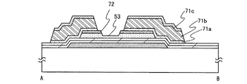
本実施の形態では、実施の形態1と同様に、被膜との界面における結晶性が高く、また膜中の結晶性も高い微結晶半導体膜を形成する工程について、図2を用いて説明する。
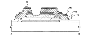
本実施の形態では、被膜との界面における結晶性が高く、また隣接する結晶粒の密着性が高い、即ち欠陥の少ない微結晶半導体膜の作製工程について、図3を用いて説明する。
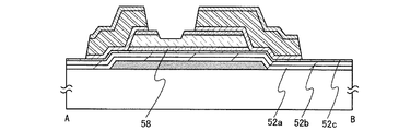
本実施の形態では、上記実施の形態1乃至実施の形態3に示す微結晶半導体膜を用いた薄膜トランジスタの作製工程について示す。本実施の形態では、微結晶半導体膜の作製方法として実施の形態1を用いて示すが、実施の形態2及び実施の形態3を適宜適用することが可能である。
本実施の形態では、実施の形態4の薄膜トランジスタの微結晶半導体膜45の形成工程において、実施の形態3に示すようなドナーとなる不純物元素を含む微結晶半導体膜の形成工程を用いた薄膜トランジスタの構造について、以下に示す。
本実施の形態では、表示装置の一形態として、実施の形態3で示す薄膜トランジスタを有する液晶表示装置について、以下に示す。ここでは、VA(Vertical Alignment)型の液晶表示装置について、図20乃至図22を用いて説明する。VA型の液晶表示装置とは、液晶パネルの液晶分子の配列を制御する方式の一種である。VA型の液晶表示装置は、電圧が印加されていないときにパネル面に対して液晶分子が垂直方向を向く方式である。本実施の形態では、特に画素(ピクセル)をいくつかの領域(サブピクセル)に分け、それぞれ別の方向に分子を倒すよう工夫されている。これをマルチドメイン化あるいはマルチドメイン設計という。以下の説明では、マルチドメイン設計が考慮された液晶表示装置について説明する。
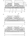
本実施の形態では、表示装置の一形態として、実施の形態3で示す薄膜トランジスタを有する発光表示装置について、以下に示す。ここでは、発光表示装置が有する画素の構成について説明する。図23(A)に、画素の上面図の一形態を示し、図23(B)に図23(A)のA−Bに対応する画素の断面構造の一形態を示す。
次に、本発明の一形態である表示パネルの構成について、以下に示す。
上記実施の形態により得られる表示装置等によって、アクティブマトリクス型表示装置パネルに用いることができる。即ち、それらを表示部に組み込んだ電子機器全てに上記実施の形態を実施できる。
本実施の形態では、実施の形態1乃至3の微結晶半導体膜を用いた光電変換素子の作製工程について、図28を用いて示す。
試料1の微結晶シリコン膜の成膜条件は、RF電源周波数を13.56MHzとし、成膜温度を280℃とし、水素流量とシランガス流量の比を150:1とし、280Paの圧力とし、RF電源の電力を50WとしたプラズマCVD法により、厚さ50nmの微結晶シリコン膜を成膜した。このときの微結晶シリコン膜のラマン散乱スペクトルを図33に示す。
試料2のアモルファスシリコン膜の成膜条件は、RF電源周波数を13.56MHzとし、成膜温度を280℃とし、水素流量とシランガス流量の比を15:14とし、170Paの圧力とし、RF電源の電力を60WとしたプラズマCVD法により、5nmのアモルファスシリコン膜を成膜した。
試料3のアモルファスシリコン膜の成膜条件は、RF電源周波数を13.56MHzとし、成膜温度を280℃とし、水素流量とシランガス流量の比を15:14とし、170Paの圧力とし、RF電源の電力を60WとしたプラズマCVD法により、5nmのアモルファスシリコン膜を成膜した。
試料4のアモルファスシリコン膜の成膜条件は、RF電源周波数を13.56MHzとし、成膜温度を280℃とし、水素流量とシランガス流量の比を15:14とし、170Paの圧力とし、RF電源の電力を60WとしたプラズマCVD法により、5nmのアモルファスシリコン膜を成膜した。
Claims (6)
- フッ素、フッ化物気体、または水素の少なくとも一つ以上を導入し高周波電力を印加して、被膜の一部をエッチングする第1の工程と、
前記被膜上に半導体膜を形成する第2の工程と、
フッ素、フッ化物気体、または水素の少なくとも一つ以上を導入し高周波電力を印加して、前記半導体膜の一部をエッチングする第3の工程と、
シリコンまたはゲルマニウムを含む堆積性気体、フッ化物気体またはフッ素、及び水素を導入し高周波電力を印加して前記被膜上に微結晶半導体膜を形成する第4の工程と、を有することを特徴とする微結晶半導体膜の作製方法。 - ドナーとなる不純物元素を含む気体を流す第1の工程と、
前記被膜上に半導体膜を形成する第2の工程と、
フッ素、フッ化物気体、または水素の少なくとも一つ以上を導入し高周波電力を印加して、前記半導体膜の一部をエッチングする第3の工程と、
シリコンまたはゲルマニウムを含む堆積性気体、フッ化物気体またはフッ素、及び水素を導入し高周波電力を印加して前記被膜上に微結晶半導体膜を形成する第4の工程と、を有することを特徴とする微結晶半導体膜の作製方法。 - 請求項1または2において、
前記第3の工程において、前記フッ素、フッ化物気体、または水素の少なくとも一つ以上と共に、ドナーとなる不純物元素を含む気体を導入し高周波電力を印加して、前記半導体膜の一部をエッチングすると共に、前記エッチングされた半導体膜に前記ドナーとなる不純物元素を添加することを特徴とする微結晶半導体膜の作製方法。 - ゲート絶縁膜を形成する第1の工程と、
フッ素、フッ化物気体、または水素の少なくとも一つ以上を導入し高周波電力を印加して、前記ゲート絶縁膜の一部をエッチングする第2の工程と、
前記ゲート絶縁膜上に半導体膜を形成する第3の工程と、
フッ素、フッ化物気体、または水素の少なくとも一つ以上を導入し高周波電力を印加して、前記半導体膜の一部をエッチングする第4の工程と、
シリコンまたはゲルマニウムを含む堆積性気体、フッ化物気体またはフッ素、及び水素を導入し高周波電力を印加して前記ゲート絶縁膜上に微結晶半導体膜を形成する第5の工程と、を有し、
前記ゲート絶縁膜、及び前記微結晶半導体膜を用いて薄膜トランジスタを作製することを特徴とする薄膜トランジスタの作製方法。 - ゲート絶縁膜を形成する第1の工程と、
ドナーとなる不純物元素を含む気体を流す第2の工程と、
前記ゲート絶縁膜上に半導体膜を形成する第3の工程と、
フッ素、フッ化物気体、または水素の少なくとも一つ以上を導入し高周波電力を印加して、前記半導体膜の一部をエッチングする第4の工程と、
シリコンまたはゲルマニウムを含む堆積性気体、フッ化物気体またはフッ素、及び水素を導入し高周波電力を印加して前記ゲート絶縁膜上に微結晶半導体膜を形成する第5の工程と、を有し、
前記ゲート絶縁膜、及び前記微結晶半導体膜を用いて薄膜トランジスタを作製することを特徴とする薄膜トランジスタの作製方法。 - 請求項4または5において、
前記第4の工程において、前記フッ素、フッ化物気体、または水素の少なくとも一つ以上と共に、ドナーとなる不純物元素を含む気体を導入し高周波電力を印加して、前記半導体膜の一部をエッチングすると共に、前記エッチングされた半導体膜に前記ドナーとなる不純物元素を添加することを特徴とする薄膜トランジスタの作製方法。
Priority Applications (1)
| Application Number | Priority Date | Filing Date | Title |
|---|---|---|---|
| JP2008307050A JP5101471B2 (ja) | 2007-12-03 | 2008-12-02 | 微結晶半導体膜及び薄膜トランジスタの作製方法 |
Applications Claiming Priority (3)
| Application Number | Priority Date | Filing Date | Title |
|---|---|---|---|
| JP2007312670 | 2007-12-03 | ||
| JP2007312670 | 2007-12-03 | ||
| JP2008307050A JP5101471B2 (ja) | 2007-12-03 | 2008-12-02 | 微結晶半導体膜及び薄膜トランジスタの作製方法 |
Publications (3)
| Publication Number | Publication Date |
|---|---|
| JP2009158947A JP2009158947A (ja) | 2009-07-16 |
| JP2009158947A5 JP2009158947A5 (ja) | 2011-12-22 |
| JP5101471B2 true JP5101471B2 (ja) | 2012-12-19 |
Family
ID=40676166
Family Applications (1)
| Application Number | Title | Priority Date | Filing Date |
|---|---|---|---|
| JP2008307050A Expired - Fee Related JP5101471B2 (ja) | 2007-12-03 | 2008-12-02 | 微結晶半導体膜及び薄膜トランジスタの作製方法 |
Country Status (3)
| Country | Link |
|---|---|
| US (1) | US8187956B2 (ja) |
| JP (1) | JP5101471B2 (ja) |
| KR (1) | KR101534099B1 (ja) |
Families Citing this family (22)
| Publication number | Priority date | Publication date | Assignee | Title |
|---|---|---|---|---|
| TWI521712B (zh) * | 2007-12-03 | 2016-02-11 | 半導體能源研究所股份有限公司 | 薄膜電晶體,包括該薄膜電晶體的顯示裝置,和其製造方法 |
| US8591650B2 (en) * | 2007-12-03 | 2013-11-26 | Semiconductor Energy Laboratory Co., Ltd. | Method for forming crystalline semiconductor film, method for manufacturing thin film transistor, and method for manufacturing display device |
| JP5395415B2 (ja) * | 2007-12-03 | 2014-01-22 | 株式会社半導体エネルギー研究所 | 薄膜トランジスタの作製方法 |
| JP5527966B2 (ja) | 2007-12-28 | 2014-06-25 | 株式会社半導体エネルギー研究所 | 薄膜トランジスタ |
| TWI371223B (en) * | 2008-02-20 | 2012-08-21 | Chimei Innolux Corp | Organic light emitting display device and fabrications thereof and electronic device |
| US7989325B2 (en) * | 2009-01-13 | 2011-08-02 | Semiconductor Energy Laboratory Co., Ltd. | Method for manufacturing crystalline semiconductor film and method for manufacturing thin film transistor |
| KR101739154B1 (ko) | 2009-07-17 | 2017-05-23 | 가부시키가이샤 한도오따이 에네루기 켄큐쇼 | 반도체 장치 및 그 제조 방법 |
| US8258025B2 (en) * | 2009-08-07 | 2012-09-04 | Semiconductor Energy Laboratory Co., Ltd. | Method for manufacturing microcrystalline semiconductor film and thin film transistor |
| JP5466933B2 (ja) * | 2009-12-03 | 2014-04-09 | 株式会社ジャパンディスプレイ | 薄膜トランジスタおよびその製造方法 |
| WO2011080957A1 (ja) * | 2009-12-29 | 2011-07-07 | シャープ株式会社 | 薄膜トランジスタ、その製造方法、および表示装置 |
| US8383434B2 (en) * | 2010-02-22 | 2013-02-26 | Semiconductor Energy Laboratory Co., Ltd. | Thin film transistor and manufacturing method thereof |
| US8343858B2 (en) * | 2010-03-02 | 2013-01-01 | Semiconductor Energy Laboratory Co., Ltd. | Method for manufacturing microcrystalline semiconductor film and method for manufacturing semiconductor device |
| JP2011210940A (ja) * | 2010-03-30 | 2011-10-20 | Casio Computer Co Ltd | 薄膜トランジスタ、薄膜トランジスタの製造方法及び発光装置 |
| JP5785770B2 (ja) * | 2010-05-14 | 2015-09-30 | 株式会社半導体エネルギー研究所 | 微結晶半導体膜の作製方法、及び半導体装置の作製方法 |
| US8884297B2 (en) * | 2010-05-14 | 2014-11-11 | Semiconductor Energy Laboratory Co., Ltd. | Microcrystalline silicon film, manufacturing method thereof, semiconductor device, and manufacturing method thereof |
| US20130087802A1 (en) * | 2010-07-07 | 2013-04-11 | Akihiko Kohno | Thin film transistor, fabrication method therefor, and display device |
| CN102386072B (zh) * | 2010-08-25 | 2016-05-04 | 株式会社半导体能源研究所 | 微晶半导体膜的制造方法及半导体装置的制造方法 |
| US8450158B2 (en) * | 2010-11-04 | 2013-05-28 | Semiconductor Energy Laboratory Co., Ltd. | Method for forming microcrystalline semiconductor film and method for manufacturing semiconductor device |
| WO2012086481A1 (ja) * | 2010-12-21 | 2012-06-28 | シャープ株式会社 | 半導体装置およびその製造方法 |
| US9111775B2 (en) | 2011-01-28 | 2015-08-18 | Semiconductor Energy Laboratory Co., Ltd. | Silicon structure and manufacturing methods thereof and of capacitor including silicon structure |
| JP5832780B2 (ja) | 2011-05-24 | 2015-12-16 | 株式会社半導体エネルギー研究所 | 半導体装置の製造方法 |
| CN109155328B (zh) * | 2018-08-10 | 2023-04-04 | 京东方科技集团股份有限公司 | 显示基板、显示面板、显示设备和制造显示基板的方法 |
Family Cites Families (49)
| Publication number | Priority date | Publication date | Assignee | Title |
|---|---|---|---|---|
| US2968866A (en) * | 1958-05-21 | 1961-01-24 | Sylvania Electric Prod | Method of producing thin wafers of semiconductor materials |
| US4251287A (en) * | 1979-10-01 | 1981-02-17 | The University Of Delaware | Amorphous semiconductor solar cell |
| JPS5685792A (en) * | 1979-12-14 | 1981-07-13 | Citizen Watch Co Ltd | Liquid crystal display unit |
| JPS56122123A (en) * | 1980-03-03 | 1981-09-25 | Shunpei Yamazaki | Semiamorphous semiconductor |
| USRE34658E (en) * | 1980-06-30 | 1994-07-12 | Semiconductor Energy Laboratory Co., Ltd. | Semiconductor device of non-single crystal-structure |
| US4727044A (en) * | 1984-05-18 | 1988-02-23 | Semiconductor Energy Laboratory Co., Ltd. | Method of making a thin film transistor with laser recrystallized source and drain |
| JPS6262073A (ja) | 1985-09-11 | 1987-03-18 | Ishikawajima Harima Heavy Ind Co Ltd | ポペツト弁の温度制御装置 |
| US4859553A (en) * | 1987-05-04 | 1989-08-22 | Xerox Corporation | Imaging members with plasma deposited silicon oxides |
| JPH0253941A (ja) | 1988-08-17 | 1990-02-22 | Tsudakoma Corp | 織機の運転装置 |
| US5514879A (en) * | 1990-11-20 | 1996-05-07 | Semiconductor Energy Laboratory Co., Ltd. | Gate insulated field effect transistors and method of manufacturing the same |
| US5849601A (en) * | 1990-12-25 | 1998-12-15 | Semiconductor Energy Laboratory Co., Ltd. | Electro-optical device and method for manufacturing the same |
| US7115902B1 (en) * | 1990-11-20 | 2006-10-03 | Semiconductor Energy Laboratory Co., Ltd. | Electro-optical device and method for manufacturing the same |
| JP2791422B2 (ja) | 1990-12-25 | 1998-08-27 | 株式会社 半導体エネルギー研究所 | 電気光学装置およびその作製方法 |
| KR950013784B1 (ko) * | 1990-11-20 | 1995-11-16 | 가부시키가이샤 한도오따이 에네루기 겐큐쇼 | 반도체 전계효과 트랜지스터 및 그 제조방법과 박막트랜지스터 |
| US7576360B2 (en) * | 1990-12-25 | 2009-08-18 | Semiconductor Energy Laboratory Co., Ltd. | Electro-optical device which comprises thin film transistors and method for manufacturing the same |
| US7098479B1 (en) * | 1990-12-25 | 2006-08-29 | Semiconductor Energy Laboratory Co., Ltd. | Electro-optical device and method for manufacturing the same |
| US5843225A (en) * | 1993-02-03 | 1998-12-01 | Semiconductor Energy Laboratory Co., Ltd. | Process for fabricating semiconductor and process for fabricating semiconductor device |
| JP3497198B2 (ja) * | 1993-02-03 | 2004-02-16 | 株式会社半導体エネルギー研究所 | 半導体装置および薄膜トランジスタの作製方法 |
| US6835523B1 (en) * | 1993-05-09 | 2004-12-28 | Semiconductor Energy Laboratory Co., Ltd. | Apparatus for fabricating coating and method of fabricating the coating |
| US5932302A (en) * | 1993-07-20 | 1999-08-03 | Semiconductor Energy Laboratory Co., Ltd. | Method for fabricating with ultrasonic vibration a carbon coating |
| TW303526B (ja) * | 1994-12-27 | 1997-04-21 | Matsushita Electric Ind Co Ltd | |
| JP3907726B2 (ja) * | 1995-12-09 | 2007-04-18 | 株式会社半導体エネルギー研究所 | 微結晶シリコン膜の作製方法、半導体装置の作製方法及び光電変換装置の作製方法 |
| KR100257158B1 (ko) | 1997-06-30 | 2000-05-15 | 김영환 | 박막 트랜지스터 및 그의 제조 방법 |
| US6077722A (en) * | 1998-07-14 | 2000-06-20 | Bp Solarex | Producing thin film photovoltaic modules with high integrity interconnects and dual layer contacts |
| JP2000277439A (ja) | 1999-03-25 | 2000-10-06 | Kanegafuchi Chem Ind Co Ltd | 結晶質シリコン系薄膜のプラズマcvd方法およびシリコン系薄膜光電変換装置の製造方法 |
| US6346730B1 (en) * | 1999-04-06 | 2002-02-12 | Semiconductor Energy Laboratory Co., Ltd. | Liquid crystal display device having a pixel TFT formed in a display region and a drive circuit formed in the periphery of the display region on the same substrate |
| JP3911971B2 (ja) * | 1999-09-08 | 2007-05-09 | 松下電器産業株式会社 | シリコン薄膜、薄膜トランジスタおよびシリコン薄膜の製造方法 |
| US6803585B2 (en) * | 2000-01-03 | 2004-10-12 | Yuri Glukhoy | Electron-cyclotron resonance type ion beam source for ion implanter |
| GB0017471D0 (en) * | 2000-07-18 | 2000-08-30 | Koninkl Philips Electronics Nv | Thin film transistors and their manufacture |
| JP2002206168A (ja) * | 2000-10-24 | 2002-07-26 | Canon Inc | シリコン系薄膜の形成方法、シリコン系半導体層の形成方法及び光起電力素子 |
| JP2004014958A (ja) | 2002-06-11 | 2004-01-15 | Fuji Electric Holdings Co Ltd | 薄膜多結晶太陽電池とその製造方法 |
| EP1445802A1 (en) * | 2003-02-06 | 2004-08-11 | Centre National De La Recherche Scientifique (Cnrs) | Transistor for active matrix display, a display unit comprising the said transistor and a method for producing said transistor |
| JP4748954B2 (ja) | 2003-07-14 | 2011-08-17 | 株式会社半導体エネルギー研究所 | 液晶表示装置 |
| JP2005050905A (ja) * | 2003-07-30 | 2005-02-24 | Sharp Corp | シリコン薄膜太陽電池の製造方法 |
| KR100752214B1 (ko) * | 2003-10-16 | 2007-08-28 | 엘지.필립스 엘시디 주식회사 | 반투과형 액정표시소자의 제조방법 |
| JP2005167051A (ja) | 2003-12-04 | 2005-06-23 | Sony Corp | 薄膜トランジスタおよび薄膜トランジスタの製造方法 |
| JP4578826B2 (ja) * | 2004-02-26 | 2010-11-10 | 株式会社半導体エネルギー研究所 | 半導体装置の作製方法 |
| US20050205880A1 (en) * | 2004-03-19 | 2005-09-22 | Aya Anzai | Display device and electronic appliance |
| JP2005317855A (ja) * | 2004-04-30 | 2005-11-10 | Canon Inc | 微結晶シリコン膜の形成方法及び光起電力素子 |
| JP5036173B2 (ja) * | 2004-11-26 | 2012-09-26 | 株式会社半導体エネルギー研究所 | 半導体装置の作製方法 |
| US7502040B2 (en) * | 2004-12-06 | 2009-03-10 | Semiconductor Energy Laboratory Co., Ltd. | Display device, driving method thereof and electronic appliance |
| JP5013393B2 (ja) * | 2005-03-30 | 2012-08-29 | 東京エレクトロン株式会社 | プラズマ処理装置と方法 |
| JP4597792B2 (ja) | 2005-06-27 | 2010-12-15 | 東京エレクトロン株式会社 | 処理ガス供給構造およびプラズマ処理装置 |
| US7514374B2 (en) * | 2005-06-29 | 2009-04-07 | Oerlikon Trading Ag, Trubbach | Method for manufacturing flat substrates |
| JP4777717B2 (ja) | 2005-08-10 | 2011-09-21 | 東京エレクトロン株式会社 | 成膜方法、プラズマ処理装置および記録媒体 |
| JP5331389B2 (ja) * | 2007-06-15 | 2013-10-30 | 株式会社半導体エネルギー研究所 | 表示装置の作製方法 |
| TWI456663B (zh) * | 2007-07-20 | 2014-10-11 | Semiconductor Energy Lab | 顯示裝置之製造方法 |
| US8030147B2 (en) * | 2007-09-14 | 2011-10-04 | Semiconductor Energy Laboratory Co., Ltd. | Method for manufacturing thin film transistor and display device including the thin film transistor |
| US8591650B2 (en) * | 2007-12-03 | 2013-11-26 | Semiconductor Energy Laboratory Co., Ltd. | Method for forming crystalline semiconductor film, method for manufacturing thin film transistor, and method for manufacturing display device |
-
2008
- 2008-11-25 US US12/277,378 patent/US8187956B2/en not_active Expired - Fee Related
- 2008-12-02 JP JP2008307050A patent/JP5101471B2/ja not_active Expired - Fee Related
- 2008-12-03 KR KR1020080121661A patent/KR101534099B1/ko active IP Right Grant
Also Published As
| Publication number | Publication date |
|---|---|
| KR20090057929A (ko) | 2009-06-08 |
| KR101534099B1 (ko) | 2015-07-06 |
| US20090142909A1 (en) | 2009-06-04 |
| US8187956B2 (en) | 2012-05-29 |
| JP2009158947A (ja) | 2009-07-16 |
Similar Documents
| Publication | Publication Date | Title |
|---|---|---|
| JP5101471B2 (ja) | 微結晶半導体膜及び薄膜トランジスタの作製方法 | |
| JP5395415B2 (ja) | 薄膜トランジスタの作製方法 | |
| JP5498689B2 (ja) | 薄膜トランジスタ、及び表示装置 | |
| JP5311955B2 (ja) | 表示装置の作製方法 | |
| JP5395414B2 (ja) | 薄膜トランジスタの作製方法 | |
| JP5503857B2 (ja) | 薄膜トランジスタの作製方法 | |
| JP5412105B2 (ja) | 半導体装置、及びそれを有する表示装置 | |
| US8860030B2 (en) | Thin film transistor and display device including the same | |
| JP5311957B2 (ja) | 表示装置及びその作製方法 | |
| JP5314870B2 (ja) | 薄膜トランジスタの作製方法 | |
| JP5297629B2 (ja) | 半導体装置の作製方法 | |
| JP4825181B2 (ja) | 薄膜トランジスタの作製方法 |
Legal Events
| Date | Code | Title | Description |
|---|---|---|---|
| A521 | Request for written amendment filed |
Free format text: JAPANESE INTERMEDIATE CODE: A523 Effective date: 20111102 |
|
| A621 | Written request for application examination |
Free format text: JAPANESE INTERMEDIATE CODE: A621 Effective date: 20111102 |
|
| A977 | Report on retrieval |
Free format text: JAPANESE INTERMEDIATE CODE: A971007 Effective date: 20120713 |
|
| A131 | Notification of reasons for refusal |
Free format text: JAPANESE INTERMEDIATE CODE: A131 Effective date: 20120724 |
|
| A521 | Request for written amendment filed |
Free format text: JAPANESE INTERMEDIATE CODE: A523 Effective date: 20120827 |
|
| TRDD | Decision of grant or rejection written | ||
| A01 | Written decision to grant a patent or to grant a registration (utility model) |
Free format text: JAPANESE INTERMEDIATE CODE: A01 Effective date: 20120918 |
|
| A01 | Written decision to grant a patent or to grant a registration (utility model) |
Free format text: JAPANESE INTERMEDIATE CODE: A01 |
|
| A61 | First payment of annual fees (during grant procedure) |
Free format text: JAPANESE INTERMEDIATE CODE: A61 Effective date: 20120926 |
|
| FPAY | Renewal fee payment (event date is renewal date of database) |
Free format text: PAYMENT UNTIL: 20151005 Year of fee payment: 3 |
|
| R150 | Certificate of patent or registration of utility model |
Free format text: JAPANESE INTERMEDIATE CODE: R150 |
|
| FPAY | Renewal fee payment (event date is renewal date of database) |
Free format text: PAYMENT UNTIL: 20151005 Year of fee payment: 3 |
|
| R250 | Receipt of annual fees |
Free format text: JAPANESE INTERMEDIATE CODE: R250 |
|
| R250 | Receipt of annual fees |
Free format text: JAPANESE INTERMEDIATE CODE: R250 |
|
| LAPS | Cancellation because of no payment of annual fees |