JP5017708B2 - ダブルデータレートダイナミックランダムアクセスメモリからのデータ取り出し方法、及びデータストローブ信号提供方法 - Google Patents
ダブルデータレートダイナミックランダムアクセスメモリからのデータ取り出し方法、及びデータストローブ信号提供方法 Download PDFInfo
- Publication number
- JP5017708B2 JP5017708B2 JP2005339494A JP2005339494A JP5017708B2 JP 5017708 B2 JP5017708 B2 JP 5017708B2 JP 2005339494 A JP2005339494 A JP 2005339494A JP 2005339494 A JP2005339494 A JP 2005339494A JP 5017708 B2 JP5017708 B2 JP 5017708B2
- Authority
- JP
- Japan
- Prior art keywords
- data
- signal
- data strobe
- clock signal
- internal clock
- Prior art date
- Legal status (The legal status is an assumption and is not a legal conclusion. Google has not performed a legal analysis and makes no representation as to the accuracy of the status listed.)
- Expired - Fee Related
Links
Images


Classifications
-
- G—PHYSICS
- G11—INFORMATION STORAGE
- G11C—STATIC STORES
- G11C11/00—Digital stores characterised by the use of particular electric or magnetic storage elements; Storage elements therefor
- G11C11/21—Digital stores characterised by the use of particular electric or magnetic storage elements; Storage elements therefor using electric elements
- G11C11/34—Digital stores characterised by the use of particular electric or magnetic storage elements; Storage elements therefor using electric elements using semiconductor devices
- G11C11/40—Digital stores characterised by the use of particular electric or magnetic storage elements; Storage elements therefor using electric elements using semiconductor devices using transistors
- G11C11/401—Digital stores characterised by the use of particular electric or magnetic storage elements; Storage elements therefor using electric elements using semiconductor devices using transistors forming cells needing refreshing or charge regeneration, i.e. dynamic cells
- G11C11/4063—Auxiliary circuits, e.g. for addressing, decoding, driving, writing, sensing or timing
- G11C11/407—Auxiliary circuits, e.g. for addressing, decoding, driving, writing, sensing or timing for memory cells of the field-effect type
- G11C11/409—Read-write [R-W] circuits
- G11C11/4096—Input/output [I/O] data management or control circuits, e.g. reading or writing circuits, I/O drivers or bit-line switches
-
- G—PHYSICS
- G11—INFORMATION STORAGE
- G11C—STATIC STORES
- G11C7/00—Arrangements for writing information into, or reading information out from, a digital store
- G11C7/10—Input/output [I/O] data interface arrangements, e.g. I/O data control circuits, I/O data buffers
- G11C7/1051—Data output circuits, e.g. read-out amplifiers, data output buffers, data output registers, data output level conversion circuits
- G11C7/1057—Data output buffers, e.g. comprising level conversion circuits, circuits for adapting load
-
- G—PHYSICS
- G11—INFORMATION STORAGE
- G11C—STATIC STORES
- G11C7/00—Arrangements for writing information into, or reading information out from, a digital store
- G11C7/10—Input/output [I/O] data interface arrangements, e.g. I/O data control circuits, I/O data buffers
- G11C7/1051—Data output circuits, e.g. read-out amplifiers, data output buffers, data output registers, data output level conversion circuits
- G11C7/106—Data output latches
-
- G—PHYSICS
- G11—INFORMATION STORAGE
- G11C—STATIC STORES
- G11C7/00—Arrangements for writing information into, or reading information out from, a digital store
- G11C7/10—Input/output [I/O] data interface arrangements, e.g. I/O data control circuits, I/O data buffers
- G11C7/1051—Data output circuits, e.g. read-out amplifiers, data output buffers, data output registers, data output level conversion circuits
- G11C7/1066—Output synchronization
-
- G—PHYSICS
- G11—INFORMATION STORAGE
- G11C—STATIC STORES
- G11C7/00—Arrangements for writing information into, or reading information out from, a digital store
- G11C7/10—Input/output [I/O] data interface arrangements, e.g. I/O data control circuits, I/O data buffers
- G11C7/1072—Input/output [I/O] data interface arrangements, e.g. I/O data control circuits, I/O data buffers for memories with random access ports synchronised on clock signal pulse trains, e.g. synchronous memories, self timed memories
-
- G—PHYSICS
- G11—INFORMATION STORAGE
- G11C—STATIC STORES
- G11C2207/00—Indexing scheme relating to arrangements for writing information into, or reading information out from, a digital store
- G11C2207/10—Aspects relating to interfaces of memory device to external buses
- G11C2207/107—Serial-parallel conversion of data or prefetch
Description
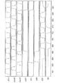
(メモリシステムバス幅)×(クロック周波数) (式1)
SDR DRAMシステムから大きいピークバンド幅を得るためには、クロックをできるだけ速くし、システムバス幅をできるだけ広く拡張する必要がある。
Claims (6)
- ダブルデータレートダイナミックランダムアクセスメモリからデータを取り出す方法であって、該方法は、
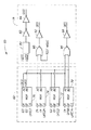
遅延ロックループを用いて外部クロック信号から、整数のクロックサイクルのレイテンシが選択されたときには、外部クロック信号の立ち下がりエッジに先行する立ち上がりエッジを有する第1内部クロック信号(DLLF0)を取り出し、外部クロック信号の立ち上がりエッジに先行する立ち上がりエッジを有する第2内部クロック信号(DLLR0)を取り出し、非整数のクロックサイクルのレイテンシが選択されたときには、外部クロック信号の立ち上がりエッジに先行する立ち上がりエッジを有する第1内部クロック信号(DLLF0)を取り出し、外部クロック信号の立ち下がりエッジに先行する立ち上がりエッジを有する第2内部クロック信号(DLLR0)を取り出す過程と、
第1内部クロック信号の立ち下がりエッジの後であって第2内部クロック信号の立ち上がりエッジの前に、データイネーブル信号を提供する過程であって、第1内部クロック信号と第2内部クロック信号とがインタリーブされる、データイネーブル信号を提供する過程と、
データイネーブル信号に応じて、第1組合せ論理回路を介して第1データアレイからの第1データを接続する過程と、
第1内部クロック信号により第1マルチプレクサを介して第1データを取り出す過程と、
データイネーブル信号に応じて、第2組合せ論理回路を介して第2データアレイからの第2データを接続する過程と、
第2内部クロック信号により第2マルチプレクサを介して第2データを取り出す過程と、
第1及び第2マルチプレクサからデータバッファへ第1及び第2データを接続する過程と、
データストローブバッファへデータストローブ信号を提供する過程であって、該データストローブ信号は、第1及び第2データに、並びに外部クロック信号に周波数が同期化されている、データストローブ信号を提供する過程と、
からなることを特徴とするデータ取り出し方法。 - 請求項1に記載の方法において、前記第1及び第2データをデータバッファへ接続する過程は、所定の遅延量を提供するための論理素子を介して第1及び第2データを接続する過程を含むことを特徴とする方法。
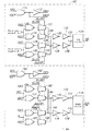
- 請求項2に記載の方法において、前記データストローブ信号を提供する過程は、
第1内部クロック信号の立ち下がりエッジの後であって第2内部クロック信号の立ち上がりエッジの前に、データストローブイネーブル信号を提供する過程と、
データストローブバッファへ接続する、第1位相関係を有するデータストローブ信号を提供するために、第1内部クロック信号により第3のマルチプレクサを介してデータストローブ信号を取り出す過程と、
データストローブバッファへ接続する、第2位相関係を有するデータストローブ信号を提供するために、第2クロック信号により第4のマルチプレクサを介してデータストローブ信号を取り出す過程と、
データストローブバッファへ、第1及び第2データと周波数が同期化され且つ外部クロック信号と所定の位相又は遅延の関係を有するデータストローブ信号を提供するために、第3及び第4のマルチプレクサからのデータストローブ信号を用いて、第1及び第2位相関係を有するデータストローブ信号をデータストローブバッファへ接続する過程と、
を含むことを特徴とする方法。 - 請求項3に記載の方法であって、更に、
データイネーブル信号をワンショット回路の第1入力に接続する過程と、
データストローブイネーブル信号をワンショット回路の第2入力に接続する過程と、
データストローブイネーブル信号とデータイネーブル信号が異なるロジック状態のときに、ワンショット回路により1クロックサイクルのパルス幅を有するパルスを生成する過程と、
所定の遅延量を提供するために、論理素子を介してパルスを接続する過程と、
データストローブ信号のためのプリアンブルを提供するために、論理素子からデータストローブバッファへパルスを接続する過程と、
を含むことを特徴とする方法。 - データストローブ信号を提供する方法であって、該方法は、
遅延ロックループを用いて外部クロック信号から、整数のクロックサイクルのレイテンシが選択されたときには、外部クロック信号の立ち下がりエッジに先行する立ち上がりエッジを有する第1内部クロック信号(DLLF0)を得、外部クロック信号の立ち上がりエッジに先行する立ち上がりエッジを有する第2内部クロック信号(DLLR0)を得、非整数のクロックサイクルのレイテンシが選択されたときには、外部クロック信号の立ち上がりエッジに先行する立ち上がりエッジを有する第1内部クロック信号(DLLF0)を得、外部クロック信号の立ち下がりエッジに先行する立ち上がりエッジを有する第2内部クロック信号(DLLR0)を得る過程と、
第1内部クロック信号の立ち下がりエッジの後であって第2内部クロック信号の立ち上がりエッジの前に、データストローブイネーブル信号を提供する過程であって、第1内部クロック信号と第2内部クロック信号とがインタリーブされているデータストローブイネーブル信号を提供する過程と、
データストローブバッファへ接続する、第1位相関係を有するデータストローブ信号を提供するために、第1内部クロック信号により第3マルチプレクサを介してデータストローブ信号を取り出す過程と、
データストローブバッファへ接続する、第2位相関係を有するデータストローブ信号を提供するために、第2内部クロック信号により第4マルチプレクサを介してデータストローブ信号を取り出す過程と、
データストローブバッファへデータストローブ信号を提供するために、第3及び第4のマルチプレクサからのデータストローブ信号を用いて、第1及び第2位相関係を有するデータストローブ信号をデータストローブバッファへ接続する過程であって、データストローブ信号は、第1及び第2データと、並びに外部クロック信号と周波数が同期化されている、第1及び第2位相関係を有するデータストローブ信号を接続する過程と、
を含むことを特徴とする方法。 - 請求項5に記載の方法であって、更に、
データイネーブル信号をワンショット回路の第1入力に接続する過程と、
データストローブイネーブル信号をワンショット回路の第2入力に接続する過程と、
データストローブイネーブル信号とデータイネーブル信号が異なるロジック状態のときに、ワンショット回路により1クロックサイクルのパルス幅を有するパルスを生成する過程と、
所定の遅延量を提供するために、論理素子を介してパルスを接続する過程と、
データストローブ信号のためのプリアンブルを提供するために、論理素子からデータストローブバッファへパルスを接続する過程と、
を含むことを特徴とする方法。
Applications Claiming Priority (2)
| Application Number | Priority Date | Filing Date | Title |
|---|---|---|---|
| US09/389,531 | 1999-09-02 | ||
| US09/389,531 US6240042B1 (en) | 1999-09-02 | 1999-09-02 | Output circuit for a double data rate dynamic random access memory, double data rate dynamic random access memory, method of clocking data out from a double data rate dynamic random access memory and method of providing a data strobe signal |
Related Parent Applications (1)
| Application Number | Title | Priority Date | Filing Date |
|---|---|---|---|
| JP2001520416A Division JP2003508872A (ja) | 1999-09-02 | 2000-08-31 | ダブルデータレートダイナミックランダムアクセスメモリ用出力回路、ダブルデータレートダイナミックランダムアクセスメモリ、ダブルデータレートダイナミックランダムアクセスメモリからのデータ取り出し方法、及びデータストローブ信号提供方法 |
Publications (2)
| Publication Number | Publication Date |
|---|---|
| JP2006172695A JP2006172695A (ja) | 2006-06-29 |
| JP5017708B2 true JP5017708B2 (ja) | 2012-09-05 |
Family
ID=23538652
Family Applications (3)
| Application Number | Title | Priority Date | Filing Date |
|---|---|---|---|
| JP2001520416A Pending JP2003508872A (ja) | 1999-09-02 | 2000-08-31 | ダブルデータレートダイナミックランダムアクセスメモリ用出力回路、ダブルデータレートダイナミックランダムアクセスメモリ、ダブルデータレートダイナミックランダムアクセスメモリからのデータ取り出し方法、及びデータストローブ信号提供方法 |
| JP2005339494A Expired - Fee Related JP5017708B2 (ja) | 1999-09-02 | 2005-11-24 | ダブルデータレートダイナミックランダムアクセスメモリからのデータ取り出し方法、及びデータストローブ信号提供方法 |
| JP2005339491A Expired - Fee Related JP4787988B2 (ja) | 1999-09-02 | 2005-11-24 | ダブルデータレートダイナミックランダムアクセスメモリ用出力回路、及びダブルデータレートダイナミックランダムアクセスメモリ |
Family Applications Before (1)
| Application Number | Title | Priority Date | Filing Date |
|---|---|---|---|
| JP2001520416A Pending JP2003508872A (ja) | 1999-09-02 | 2000-08-31 | ダブルデータレートダイナミックランダムアクセスメモリ用出力回路、ダブルデータレートダイナミックランダムアクセスメモリ、ダブルデータレートダイナミックランダムアクセスメモリからのデータ取り出し方法、及びデータストローブ信号提供方法 |
Family Applications After (1)
| Application Number | Title | Priority Date | Filing Date |
|---|---|---|---|
| JP2005339491A Expired - Fee Related JP4787988B2 (ja) | 1999-09-02 | 2005-11-24 | ダブルデータレートダイナミックランダムアクセスメモリ用出力回路、及びダブルデータレートダイナミックランダムアクセスメモリ |
Country Status (8)
| Country | Link |
|---|---|
| US (2) | US6240042B1 (ja) |
| JP (3) | JP2003508872A (ja) |
| KR (1) | KR100493477B1 (ja) |
| AU (1) | AU7342200A (ja) |
| DE (1) | DE10084993B3 (ja) |
| GB (1) | GB2368947B (ja) |
| TW (1) | TW546668B (ja) |
| WO (1) | WO2001016957A1 (ja) |
Families Citing this family (67)
| Publication number | Priority date | Publication date | Assignee | Title |
|---|---|---|---|---|
| GB2393004B (en) * | 1999-09-02 | 2004-06-23 | Micron Technology Inc | Apparatus for analogue information transfer |
| JP2002108693A (ja) * | 2000-10-03 | 2002-04-12 | Fujitsu Ltd | データ読み出し方法、メモリコントローラ及び半導体集積回路装置 |
| US6377096B1 (en) * | 2000-10-24 | 2002-04-23 | Hewlett-Packard Company | Static to dynamic logic interface circuit |
| US6546461B1 (en) | 2000-11-22 | 2003-04-08 | Integrated Device Technology, Inc. | Multi-port cache memory devices and FIFO memory devices having multi-port cache memory devices therein |
| US6889336B2 (en) * | 2001-01-05 | 2005-05-03 | Micron Technology, Inc. | Apparatus for improving output skew for synchronous integrate circuits has delay circuit for generating unique clock signal by applying programmable delay to delayed clock signal |
| US6570813B2 (en) | 2001-05-25 | 2003-05-27 | Micron Technology, Inc. | Synchronous mirror delay with reduced delay line taps |
| US6876239B2 (en) * | 2001-07-11 | 2005-04-05 | Micron Technology, Inc. | Delay locked loop “ACTIVE command” reactor |
| US6795360B2 (en) * | 2001-08-23 | 2004-09-21 | Integrated Device Technology, Inc. | Fifo memory devices that support all four combinations of DDR or SDR write modes with DDR or SDR read modes |
| US7082071B2 (en) * | 2001-08-23 | 2006-07-25 | Integrated Device Technology, Inc. | Integrated DDR/SDR flow control managers that support multiple queues and MUX, DEMUX and broadcast operating modes |
| US6577552B2 (en) | 2001-08-30 | 2003-06-10 | Micron Technology, Inc. | Apparatus and method for generating an oscillating signal |
| US6930524B2 (en) * | 2001-10-09 | 2005-08-16 | Micron Technology, Inc. | Dual-phase delay-locked loop circuit and method |
| KR100446291B1 (ko) | 2001-11-07 | 2004-09-01 | 삼성전자주식회사 | 카스 레이턴시를 이용하여 락킹 레졸루션 조절이 가능한지연동기 루프 회로 |
| US6759911B2 (en) | 2001-11-19 | 2004-07-06 | Mcron Technology, Inc. | Delay-locked loop circuit and method using a ring oscillator and counter-based delay |
| US6597628B1 (en) * | 2002-01-08 | 2003-07-22 | 3Dlabs, Inc., Ltd | Auto-disable receive control for DDR receive strobes |
| US6950350B1 (en) * | 2002-01-08 | 2005-09-27 | #Dlabs, Inc., Ltd. | Configurable pipe delay with window overlap for DDR receive data |
| KR100470995B1 (ko) * | 2002-04-23 | 2005-03-08 | 삼성전자주식회사 | 클럭수신 동기회로를 갖는 멀티클럭 도메인 데이터 입력처리장치 및 그에 따른 클럭신호 인가방법 |
| US6801070B2 (en) | 2002-05-16 | 2004-10-05 | Micron Technology, Inc. | Measure-controlled circuit with frequency control |
| US7319728B2 (en) | 2002-05-16 | 2008-01-15 | Micron Technology, Inc. | Delay locked loop with frequency control |
| US6943044B1 (en) * | 2002-06-11 | 2005-09-13 | Etron Technology, Inc. | Method of high speed data rate testing |
| US6621316B1 (en) | 2002-06-20 | 2003-09-16 | Micron Technology, Inc. | Synchronous mirror delay (SMD) circuit and method including a counter and reduced size bi-directional delay line |
| US6809990B2 (en) * | 2002-06-21 | 2004-10-26 | Micron Technology, Inc. | Delay locked loop control circuit |
| US6819599B2 (en) * | 2002-08-01 | 2004-11-16 | Micron Technology, Inc. | Programmable DQS preamble |
| US6727740B2 (en) | 2002-08-29 | 2004-04-27 | Micron Technology, Inc. | Synchronous mirror delay (SMD) circuit and method including a ring oscillator for timing coarse and fine delay intervals |
| US6687185B1 (en) * | 2002-08-29 | 2004-02-03 | Micron Technology, Inc. | Method and apparatus for setting and compensating read latency in a high speed DRAM |
| US7010713B2 (en) | 2002-12-19 | 2006-03-07 | Mosaid Technologies, Inc. | Synchronization circuit and method with transparent latches |
| US7738496B1 (en) | 2002-12-31 | 2010-06-15 | Cypress Semiconductor Corporation | Device that provides the functionality of dual-ported memory using single-ported memory for multiple clock domains |
| US6762974B1 (en) * | 2003-03-18 | 2004-07-13 | Micron Technology, Inc. | Method and apparatus for establishing and maintaining desired read latency in high-speed DRAM |
| US6839301B2 (en) * | 2003-04-28 | 2005-01-04 | Micron Technology, Inc. | Method and apparatus for improving stability and lock time for synchronous circuits |
| KR100522433B1 (ko) * | 2003-04-29 | 2005-10-20 | 주식회사 하이닉스반도체 | 도메인 크로싱 회로 |
| US7177379B1 (en) | 2003-04-29 | 2007-02-13 | Advanced Micro Devices, Inc. | DDR on-the-fly synchronization |
| KR100927395B1 (ko) * | 2003-04-29 | 2009-11-19 | 주식회사 하이닉스반도체 | 데이터 인 스트로브 신호 발생 장치 |
| TWI303427B (en) * | 2003-04-30 | 2008-11-21 | Hynix Semiconductor Inc | Synchronous memory device having advanced data align circuit |
| US6937076B2 (en) * | 2003-06-11 | 2005-08-30 | Micron Technology, Inc. | Clock synchronizing apparatus and method using frequency dependent variable delay |
| US7685456B1 (en) | 2003-07-30 | 2010-03-23 | Marvell Israel (Misl) Ltd. | DDR interface bus control |
| US7120075B1 (en) | 2003-08-18 | 2006-10-10 | Integrated Device Technology, Inc. | Multi-FIFO integrated circuit devices that support multi-queue operating modes with enhanced write path and read path queue switching |
| US7031205B2 (en) * | 2003-09-29 | 2006-04-18 | Infineon Technologies North America Corp. | Random access memory with post-amble data strobe signal noise rejection |
| US20050073901A1 (en) * | 2003-10-06 | 2005-04-07 | Infineon Technologies North America Corp. | Random access memory with data strobe locking circuit |
| KR100557636B1 (ko) * | 2003-12-23 | 2006-03-10 | 주식회사 하이닉스반도체 | 클럭신호를 이용한 데이터 스트로브 회로 |
| US7934057B1 (en) * | 2003-12-24 | 2011-04-26 | Cypress Semiconductor Corporation | Logic for implementing a dual clock domain read access with predictable timing for bi-directional inputs/outputs |
| KR100521049B1 (ko) | 2003-12-30 | 2005-10-11 | 주식회사 하이닉스반도체 | 더블 데이터 레이트 싱크로너스 디램의 쓰기 회로 |
| US7042792B2 (en) * | 2004-01-14 | 2006-05-09 | Integrated Device Technology, Inc. | Multi-port memory cells for use in FIFO applications that support data transfers between cache and supplemental memory arrays |
| US7078950B2 (en) * | 2004-07-20 | 2006-07-18 | Micron Technology, Inc. | Delay-locked loop with feedback compensation |
| KR100668829B1 (ko) | 2004-10-12 | 2007-01-16 | 주식회사 하이닉스반도체 | 메모리 장치용 데이타 출력 제어 회로 |
| KR100636929B1 (ko) * | 2004-11-15 | 2006-10-19 | 주식회사 하이닉스반도체 | 메모리 장치의 데이터 출력 회로 |
| US7466783B2 (en) * | 2004-12-13 | 2008-12-16 | Lexmark International, Inc. | Method and system to implement a double data rate (DDR) interface |
| US7130226B2 (en) * | 2005-02-09 | 2006-10-31 | Micron Technology, Inc. | Clock generating circuit with multiple modes of operation |
| US7233543B2 (en) * | 2005-03-01 | 2007-06-19 | Hewlett-Packard Development Company, L.P. | System and method to change data window |
| US7702839B2 (en) * | 2005-04-12 | 2010-04-20 | Nokia Corporation | Memory interface for volatile and non-volatile memory devices |
| US7280417B2 (en) * | 2005-04-26 | 2007-10-09 | Micron Technology, Inc. | System and method for capturing data signals using a data strobe signal |
| KR100755371B1 (ko) * | 2005-05-03 | 2007-09-04 | 삼성전자주식회사 | 반도체 메모리 장치 및 이 장치의 데이터 스트로우브 신호발생방법 |
| US7123524B1 (en) | 2005-05-13 | 2006-10-17 | Infineon Technologies Ag | Input circuit having updated output signal synchronized to clock signal |
| US7428603B2 (en) | 2005-06-30 | 2008-09-23 | Sigmatel, Inc. | System and method for communicating with memory devices via plurality of state machines and a DMA controller |
| US7277357B1 (en) * | 2006-06-05 | 2007-10-02 | Micron Technology, Inc. | Method and apparatus for reducing oscillation in synchronous circuits |
| US8589632B1 (en) | 2007-03-09 | 2013-11-19 | Cypress Semiconductor Corporation | Arbitration method for programmable multiple clock domain bi-directional interface |
| US8145809B1 (en) | 2007-03-09 | 2012-03-27 | Cypress Semiconductor Corporation | Busy detection logic for asynchronous communication port |
| KR100911197B1 (ko) * | 2007-12-27 | 2009-08-06 | 주식회사 하이닉스반도체 | 반도체 메모리 장치의 데이터 출력 회로 |
| KR100911201B1 (ko) | 2008-02-14 | 2009-08-06 | 주식회사 하이닉스반도체 | 반도체 메모리 장치의 데이터 스트로브 클럭 버퍼 및 그제어 방법 |
| KR100955267B1 (ko) * | 2008-04-30 | 2010-04-30 | 주식회사 하이닉스반도체 | 반도체 메모리장치 및 이의 동작 방법 |
| EP2467852B1 (en) * | 2009-08-20 | 2019-05-22 | Rambus Inc. | Atomic memory device |
| KR101132799B1 (ko) * | 2010-04-01 | 2012-04-02 | 주식회사 하이닉스반도체 | 반도체 메모리 장치 및 시스템 |
| KR101796116B1 (ko) | 2010-10-20 | 2017-11-10 | 삼성전자 주식회사 | 반도체 장치, 이를 포함하는 메모리 모듈, 메모리 시스템 및 그 동작방법 |
| RU2011115528A (ru) | 2011-04-21 | 2012-10-27 | Дженерал Электрик Компани (US) | Топливная форсунка, камера сгорания и способ работы камеры сгорания |
| JP6179206B2 (ja) * | 2013-06-11 | 2017-08-16 | 株式会社リコー | メモリ制御装置 |
| KR102211709B1 (ko) * | 2014-05-19 | 2021-02-02 | 삼성전자주식회사 | 신호 송수신 특성을 향상한 불휘발성 메모리 시스템, 호스트 장치, 불휘발성 메모리 시스템 및 호스트의 동작방법 |
| KR102323569B1 (ko) | 2015-09-30 | 2021-11-08 | 삼성전자주식회사 | 샘플링 포인트를 독립적으로 조절할 수 있는 데이터 처리 회로와 이를 포함하는 데이터 처리 시스템 |
| US10649849B2 (en) * | 2017-07-14 | 2020-05-12 | Samsung Electronics Co., Ltd. | Memory device including detection clock pattern generator for generating detection clock output signal including random data pattern |
| US10431293B1 (en) * | 2018-07-23 | 2019-10-01 | Micron Technology, Inc. | Systems and methods for controlling data strobe signals during read operations |
Family Cites Families (10)
| Publication number | Priority date | Publication date | Assignee | Title |
|---|---|---|---|---|
| US5598113A (en) * | 1995-01-19 | 1997-01-28 | Intel Corporation | Fully asynchronous interface with programmable metastability settling time synchronizer |
| US5831929A (en) | 1997-04-04 | 1998-11-03 | Micron Technology, Inc. | Memory device with staggered data paths |
| US6104225A (en) * | 1997-04-21 | 2000-08-15 | Fujitsu Limited | Semiconductor device using complementary clock and signal input state detection circuit used for the same |
| JP3901297B2 (ja) * | 1997-09-09 | 2007-04-04 | 富士通株式会社 | Dll回路及びそれを利用した半導体記憶装置 |
| JP3788867B2 (ja) * | 1997-10-28 | 2006-06-21 | 株式会社東芝 | 半導体記憶装置 |
| KR100252057B1 (ko) | 1997-12-30 | 2000-05-01 | 윤종용 | 단일 및 이중 데이터 율 겸용 반도체 메모리 장치 |
| KR100278653B1 (ko) * | 1998-01-23 | 2001-02-01 | 윤종용 | 이중 데이터율 모드 반도체 메모리 장치 |
| JPH11213666A (ja) | 1998-01-30 | 1999-08-06 | Mitsubishi Electric Corp | 出力回路および同期型半導体記憶装置 |
| US5923613A (en) | 1998-03-18 | 1999-07-13 | Etron Technology, Inc. | Latched type clock synchronizer with additional 180°-phase shift clock |
| US6043694A (en) * | 1998-06-24 | 2000-03-28 | Siemens Aktiengesellschaft | Lock arrangement for a calibrated DLL in DDR SDRAM applications |
-
1999
- 1999-09-02 US US09/389,531 patent/US6240042B1/en not_active Expired - Lifetime
-
2000
- 2000-08-31 JP JP2001520416A patent/JP2003508872A/ja active Pending
- 2000-08-31 WO PCT/US2000/024076 patent/WO2001016957A1/en active IP Right Grant
- 2000-08-31 DE DE10084993T patent/DE10084993B3/de not_active Expired - Fee Related
- 2000-08-31 AU AU73422/00A patent/AU7342200A/en not_active Abandoned
- 2000-08-31 GB GB0204835A patent/GB2368947B/en not_active Expired - Fee Related
- 2000-08-31 KR KR10-2002-7002668A patent/KR100493477B1/ko not_active IP Right Cessation
- 2000-09-01 TW TW089117939A patent/TW546668B/zh not_active IP Right Cessation
-
2001
- 2001-04-20 US US09/838,861 patent/US6381194B2/en not_active Expired - Lifetime
-
2005
- 2005-11-24 JP JP2005339494A patent/JP5017708B2/ja not_active Expired - Fee Related
- 2005-11-24 JP JP2005339491A patent/JP4787988B2/ja not_active Expired - Fee Related
Also Published As
| Publication number | Publication date |
|---|---|
| JP4787988B2 (ja) | 2011-10-05 |
| US6240042B1 (en) | 2001-05-29 |
| DE10084993B3 (de) | 2013-03-21 |
| KR20030009292A (ko) | 2003-01-29 |
| KR100493477B1 (ko) | 2005-06-03 |
| GB2368947B (en) | 2004-02-18 |
| US20010014053A1 (en) | 2001-08-16 |
| AU7342200A (en) | 2001-03-26 |
| US6381194B2 (en) | 2002-04-30 |
| JP2006172695A (ja) | 2006-06-29 |
| JP2006120311A (ja) | 2006-05-11 |
| WO2001016957A1 (en) | 2001-03-08 |
| GB2368947A (en) | 2002-05-15 |
| GB0204835D0 (en) | 2002-04-17 |
| TW546668B (en) | 2003-08-11 |
| DE10084993T1 (de) | 2002-08-01 |
| JP2003508872A (ja) | 2003-03-04 |
Similar Documents
| Publication | Publication Date | Title |
|---|---|---|
| JP5017708B2 (ja) | ダブルデータレートダイナミックランダムアクセスメモリからのデータ取り出し方法、及びデータストローブ信号提供方法 | |
| EP1068619B1 (en) | Semiconductor memory asynchronous pipeline | |
| US6151271A (en) | Integrated circuit memory devices having data selection circuits therein which are compatible with single and dual rate mode operation and methods of operating same | |
| US7415404B2 (en) | Method and apparatus for generating a sequence of clock signals | |
| US7605631B2 (en) | Delay line synchronizer apparatus and method | |
| JP3013714B2 (ja) | 半導体記憶装置 | |
| US6259288B1 (en) | Semiconductor integrated circuit having a DLL circuit and a special power supply circuit for the DLL circuit | |
| US20110298512A1 (en) | Circuit, system and method for controlling read latency | |
| US6862250B2 (en) | Circuit and method for generating output control signal in synchronous semiconductor memory device | |
| US6782459B1 (en) | Method and apparatus for controlling a read valid window of a synchronous memory device | |
| KR100623801B1 (ko) | 반도체 메모리 비동기식 파이프라인 | |
| GB2320779A (en) | Synchronous semiconductor memory device | |
| JP2001060392A (ja) | 半導体装置 | |
| KR100334480B1 (ko) | 개선된 버스트 모드 동작을 위하여 반도체 기억장치에서 사용하 | |
| US7227812B2 (en) | Write address synchronization useful for a DDR prefetch SDRAM | |
| US7181638B2 (en) | Method and apparatus for skewing data with respect to command on a DDR interface | |
| GB2393004A (en) | Output circuit for a double data rate DRAM with a data strobe signal with a preamble. | |
| JP3493176B2 (ja) | データシンクロナイザ回路 |
Legal Events
| Date | Code | Title | Description |
|---|---|---|---|
| RD03 | Notification of appointment of power of attorney |
Free format text: JAPANESE INTERMEDIATE CODE: A7423 Effective date: 20060901 |
|
| A621 | Written request for application examination |
Free format text: JAPANESE INTERMEDIATE CODE: A621 Effective date: 20070625 |
|
| RD02 | Notification of acceptance of power of attorney |
Free format text: JAPANESE INTERMEDIATE CODE: A7422 Effective date: 20070625 |
|
| RD04 | Notification of resignation of power of attorney |
Free format text: JAPANESE INTERMEDIATE CODE: A7424 Effective date: 20071004 |
|
| A977 | Report on retrieval |
Free format text: JAPANESE INTERMEDIATE CODE: A971007 Effective date: 20100413 |
|
| A131 | Notification of reasons for refusal |
Free format text: JAPANESE INTERMEDIATE CODE: A131 Effective date: 20100420 |
|
| A521 | Written amendment |
Free format text: JAPANESE INTERMEDIATE CODE: A821 Effective date: 20100716 |
|
| A601 | Written request for extension of time |
Free format text: JAPANESE INTERMEDIATE CODE: A601 Effective date: 20100716 |
|
| RD02 | Notification of acceptance of power of attorney |
Free format text: JAPANESE INTERMEDIATE CODE: A7422 Effective date: 20100716 |
|
| A602 | Written permission of extension of time |
Free format text: JAPANESE INTERMEDIATE CODE: A602 Effective date: 20100728 |
|
| A521 | Written amendment |
Free format text: JAPANESE INTERMEDIATE CODE: A523 Effective date: 20100817 Free format text: JAPANESE INTERMEDIATE CODE: A821 Effective date: 20100817 |
|
| A131 | Notification of reasons for refusal |
Free format text: JAPANESE INTERMEDIATE CODE: A131 Effective date: 20110607 |
|
| A521 | Written amendment |
Free format text: JAPANESE INTERMEDIATE CODE: A821 Effective date: 20110815 Free format text: JAPANESE INTERMEDIATE CODE: A523 Effective date: 20110815 |
|
| TRDD | Decision of grant or rejection written | ||
| A01 | Written decision to grant a patent or to grant a registration (utility model) |
Free format text: JAPANESE INTERMEDIATE CODE: A01 Effective date: 20120424 |
|
| A01 | Written decision to grant a patent or to grant a registration (utility model) |
Free format text: JAPANESE INTERMEDIATE CODE: A01 |
|
| A521 | Written amendment |
Free format text: JAPANESE INTERMEDIATE CODE: A821 Effective date: 20120523 |
|
| A711 | Notification of change in applicant |
Free format text: JAPANESE INTERMEDIATE CODE: A711 Effective date: 20120523 |
|
| A521 | Written amendment |
Free format text: JAPANESE INTERMEDIATE CODE: A821 Effective date: 20120523 |
|
| A61 | First payment of annual fees (during grant procedure) |
Free format text: JAPANESE INTERMEDIATE CODE: A61 Effective date: 20120523 |
|
| R150 | Certificate of patent or registration of utility model |
Free format text: JAPANESE INTERMEDIATE CODE: R150 |
|
| FPAY | Renewal fee payment (event date is renewal date of database) |
Free format text: PAYMENT UNTIL: 20150622 Year of fee payment: 3 |
|
| R250 | Receipt of annual fees |
Free format text: JAPANESE INTERMEDIATE CODE: R250 |
|
| R250 | Receipt of annual fees |
Free format text: JAPANESE INTERMEDIATE CODE: R250 |
|
| LAPS | Cancellation because of no payment of annual fees |