JP5009085B2 - 半導体装置 - Google Patents
半導体装置 Download PDFInfo
- Publication number
- JP5009085B2 JP5009085B2 JP2007207962A JP2007207962A JP5009085B2 JP 5009085 B2 JP5009085 B2 JP 5009085B2 JP 2007207962 A JP2007207962 A JP 2007207962A JP 2007207962 A JP2007207962 A JP 2007207962A JP 5009085 B2 JP5009085 B2 JP 5009085B2
- Authority
- JP
- Japan
- Prior art keywords
- heat
- cooling
- semiconductor
- flow path
- semiconductor device
- Prior art date
- Legal status (The legal status is an assumption and is not a legal conclusion. Google has not performed a legal analysis and makes no representation as to the accuracy of the status listed.)
- Expired - Fee Related
Links
Images


Classifications
-
- H—ELECTRICITY
- H01—ELECTRIC ELEMENTS
- H01L—SEMICONDUCTOR DEVICES NOT COVERED BY CLASS H10
- H01L23/00—Details of semiconductor or other solid state devices
- H01L23/34—Arrangements for cooling, heating, ventilating or temperature compensation ; Temperature sensing arrangements
- H01L23/46—Arrangements for cooling, heating, ventilating or temperature compensation ; Temperature sensing arrangements involving the transfer of heat by flowing fluids
- H01L23/473—Arrangements for cooling, heating, ventilating or temperature compensation ; Temperature sensing arrangements involving the transfer of heat by flowing fluids by flowing liquids
-
- H—ELECTRICITY
- H01—ELECTRIC ELEMENTS
- H01L—SEMICONDUCTOR DEVICES NOT COVERED BY CLASS H10
- H01L25/00—Assemblies consisting of a plurality of individual semiconductor or other solid state devices ; Multistep manufacturing processes thereof
- H01L25/03—Assemblies consisting of a plurality of individual semiconductor or other solid state devices ; Multistep manufacturing processes thereof all the devices being of a type provided for in the same subgroup of groups H01L27/00 - H01L33/00, or in a single subclass of H10K, H10N, e.g. assemblies of rectifier diodes
- H01L25/04—Assemblies consisting of a plurality of individual semiconductor or other solid state devices ; Multistep manufacturing processes thereof all the devices being of a type provided for in the same subgroup of groups H01L27/00 - H01L33/00, or in a single subclass of H10K, H10N, e.g. assemblies of rectifier diodes the devices not having separate containers
- H01L25/065—Assemblies consisting of a plurality of individual semiconductor or other solid state devices ; Multistep manufacturing processes thereof all the devices being of a type provided for in the same subgroup of groups H01L27/00 - H01L33/00, or in a single subclass of H10K, H10N, e.g. assemblies of rectifier diodes the devices not having separate containers the devices being of a type provided for in group H01L27/00
- H01L25/0655—Assemblies consisting of a plurality of individual semiconductor or other solid state devices ; Multistep manufacturing processes thereof all the devices being of a type provided for in the same subgroup of groups H01L27/00 - H01L33/00, or in a single subclass of H10K, H10N, e.g. assemblies of rectifier diodes the devices not having separate containers the devices being of a type provided for in group H01L27/00 the devices being arranged next to each other
-
- H—ELECTRICITY
- H01—ELECTRIC ELEMENTS
- H01L—SEMICONDUCTOR DEVICES NOT COVERED BY CLASS H10
- H01L2224/00—Indexing scheme for arrangements for connecting or disconnecting semiconductor or solid-state bodies and methods related thereto as covered by H01L24/00
- H01L2224/01—Means for bonding being attached to, or being formed on, the surface to be connected, e.g. chip-to-package, die-attach, "first-level" interconnects; Manufacturing methods related thereto
- H01L2224/10—Bump connectors; Manufacturing methods related thereto
- H01L2224/15—Structure, shape, material or disposition of the bump connectors after the connecting process
- H01L2224/16—Structure, shape, material or disposition of the bump connectors after the connecting process of an individual bump connector
- H01L2224/161—Disposition
- H01L2224/16151—Disposition the bump connector connecting between a semiconductor or solid-state body and an item not being a semiconductor or solid-state body, e.g. chip-to-substrate, chip-to-passive
- H01L2224/16221—Disposition the bump connector connecting between a semiconductor or solid-state body and an item not being a semiconductor or solid-state body, e.g. chip-to-substrate, chip-to-passive the body and the item being stacked
- H01L2224/16225—Disposition the bump connector connecting between a semiconductor or solid-state body and an item not being a semiconductor or solid-state body, e.g. chip-to-substrate, chip-to-passive the body and the item being stacked the item being non-metallic, e.g. insulating substrate with or without metallisation
- H01L2224/16227—Disposition the bump connector connecting between a semiconductor or solid-state body and an item not being a semiconductor or solid-state body, e.g. chip-to-substrate, chip-to-passive the body and the item being stacked the item being non-metallic, e.g. insulating substrate with or without metallisation the bump connector connecting to a bond pad of the item
-
- H—ELECTRICITY
- H01—ELECTRIC ELEMENTS
- H01L—SEMICONDUCTOR DEVICES NOT COVERED BY CLASS H10
- H01L2224/00—Indexing scheme for arrangements for connecting or disconnecting semiconductor or solid-state bodies and methods related thereto as covered by H01L24/00
- H01L2224/01—Means for bonding being attached to, or being formed on, the surface to be connected, e.g. chip-to-package, die-attach, "first-level" interconnects; Manufacturing methods related thereto
- H01L2224/10—Bump connectors; Manufacturing methods related thereto
- H01L2224/15—Structure, shape, material or disposition of the bump connectors after the connecting process
- H01L2224/16—Structure, shape, material or disposition of the bump connectors after the connecting process of an individual bump connector
- H01L2224/161—Disposition
- H01L2224/16151—Disposition the bump connector connecting between a semiconductor or solid-state body and an item not being a semiconductor or solid-state body, e.g. chip-to-substrate, chip-to-passive
- H01L2224/16221—Disposition the bump connector connecting between a semiconductor or solid-state body and an item not being a semiconductor or solid-state body, e.g. chip-to-substrate, chip-to-passive the body and the item being stacked
- H01L2224/16225—Disposition the bump connector connecting between a semiconductor or solid-state body and an item not being a semiconductor or solid-state body, e.g. chip-to-substrate, chip-to-passive the body and the item being stacked the item being non-metallic, e.g. insulating substrate with or without metallisation
- H01L2224/16235—Disposition the bump connector connecting between a semiconductor or solid-state body and an item not being a semiconductor or solid-state body, e.g. chip-to-substrate, chip-to-passive the body and the item being stacked the item being non-metallic, e.g. insulating substrate with or without metallisation the bump connector connecting to a via metallisation of the item
-
- H—ELECTRICITY
- H01—ELECTRIC ELEMENTS
- H01L—SEMICONDUCTOR DEVICES NOT COVERED BY CLASS H10
- H01L2224/00—Indexing scheme for arrangements for connecting or disconnecting semiconductor or solid-state bodies and methods related thereto as covered by H01L24/00
- H01L2224/01—Means for bonding being attached to, or being formed on, the surface to be connected, e.g. chip-to-package, die-attach, "first-level" interconnects; Manufacturing methods related thereto
- H01L2224/26—Layer connectors, e.g. plate connectors, solder or adhesive layers; Manufacturing methods related thereto
- H01L2224/31—Structure, shape, material or disposition of the layer connectors after the connecting process
- H01L2224/32—Structure, shape, material or disposition of the layer connectors after the connecting process of an individual layer connector
- H01L2224/321—Disposition
- H01L2224/32151—Disposition the layer connector connecting between a semiconductor or solid-state body and an item not being a semiconductor or solid-state body, e.g. chip-to-substrate, chip-to-passive
- H01L2224/32221—Disposition the layer connector connecting between a semiconductor or solid-state body and an item not being a semiconductor or solid-state body, e.g. chip-to-substrate, chip-to-passive the body and the item being stacked
- H01L2224/32225—Disposition the layer connector connecting between a semiconductor or solid-state body and an item not being a semiconductor or solid-state body, e.g. chip-to-substrate, chip-to-passive the body and the item being stacked the item being non-metallic, e.g. insulating substrate with or without metallisation
-
- H—ELECTRICITY
- H01—ELECTRIC ELEMENTS
- H01L—SEMICONDUCTOR DEVICES NOT COVERED BY CLASS H10
- H01L2224/00—Indexing scheme for arrangements for connecting or disconnecting semiconductor or solid-state bodies and methods related thereto as covered by H01L24/00
- H01L2224/01—Means for bonding being attached to, or being formed on, the surface to be connected, e.g. chip-to-package, die-attach, "first-level" interconnects; Manufacturing methods related thereto
- H01L2224/26—Layer connectors, e.g. plate connectors, solder or adhesive layers; Manufacturing methods related thereto
- H01L2224/31—Structure, shape, material or disposition of the layer connectors after the connecting process
- H01L2224/32—Structure, shape, material or disposition of the layer connectors after the connecting process of an individual layer connector
- H01L2224/321—Disposition
- H01L2224/32151—Disposition the layer connector connecting between a semiconductor or solid-state body and an item not being a semiconductor or solid-state body, e.g. chip-to-substrate, chip-to-passive
- H01L2224/32221—Disposition the layer connector connecting between a semiconductor or solid-state body and an item not being a semiconductor or solid-state body, e.g. chip-to-substrate, chip-to-passive the body and the item being stacked
- H01L2224/32245—Disposition the layer connector connecting between a semiconductor or solid-state body and an item not being a semiconductor or solid-state body, e.g. chip-to-substrate, chip-to-passive the body and the item being stacked the item being metallic
-
- H—ELECTRICITY
- H01—ELECTRIC ELEMENTS
- H01L—SEMICONDUCTOR DEVICES NOT COVERED BY CLASS H10
- H01L2224/00—Indexing scheme for arrangements for connecting or disconnecting semiconductor or solid-state bodies and methods related thereto as covered by H01L24/00
- H01L2224/73—Means for bonding being of different types provided for in two or more of groups H01L2224/10, H01L2224/18, H01L2224/26, H01L2224/34, H01L2224/42, H01L2224/50, H01L2224/63, H01L2224/71
- H01L2224/732—Location after the connecting process
- H01L2224/73201—Location after the connecting process on the same surface
- H01L2224/73203—Bump and layer connectors
- H01L2224/73204—Bump and layer connectors the bump connector being embedded into the layer connector
-
- H—ELECTRICITY
- H01—ELECTRIC ELEMENTS
- H01L—SEMICONDUCTOR DEVICES NOT COVERED BY CLASS H10
- H01L2224/00—Indexing scheme for arrangements for connecting or disconnecting semiconductor or solid-state bodies and methods related thereto as covered by H01L24/00
- H01L2224/73—Means for bonding being of different types provided for in two or more of groups H01L2224/10, H01L2224/18, H01L2224/26, H01L2224/34, H01L2224/42, H01L2224/50, H01L2224/63, H01L2224/71
- H01L2224/732—Location after the connecting process
- H01L2224/73251—Location after the connecting process on different surfaces
- H01L2224/73253—Bump and layer connectors
-
- H—ELECTRICITY
- H01—ELECTRIC ELEMENTS
- H01L—SEMICONDUCTOR DEVICES NOT COVERED BY CLASS H10
- H01L2924/00—Indexing scheme for arrangements or methods for connecting or disconnecting semiconductor or solid-state bodies as covered by H01L24/00
- H01L2924/15—Details of package parts other than the semiconductor or other solid state devices to be connected
- H01L2924/151—Die mounting substrate
- H01L2924/153—Connection portion
- H01L2924/1531—Connection portion the connection portion being formed only on the surface of the substrate opposite to the die mounting surface
- H01L2924/15311—Connection portion the connection portion being formed only on the surface of the substrate opposite to the die mounting surface being a ball array, e.g. BGA
-
- H—ELECTRICITY
- H01—ELECTRIC ELEMENTS
- H01L—SEMICONDUCTOR DEVICES NOT COVERED BY CLASS H10
- H01L2924/00—Indexing scheme for arrangements or methods for connecting or disconnecting semiconductor or solid-state bodies as covered by H01L24/00
- H01L2924/15—Details of package parts other than the semiconductor or other solid state devices to be connected
- H01L2924/161—Cap
- H01L2924/1615—Shape
- H01L2924/16152—Cap comprising a cavity for hosting the device, e.g. U-shaped cap
-
- H—ELECTRICITY
- H01—ELECTRIC ELEMENTS
- H01L—SEMICONDUCTOR DEVICES NOT COVERED BY CLASS H10
- H01L2924/00—Indexing scheme for arrangements or methods for connecting or disconnecting semiconductor or solid-state bodies as covered by H01L24/00
- H01L2924/15—Details of package parts other than the semiconductor or other solid state devices to be connected
- H01L2924/161—Cap
- H01L2924/162—Disposition
- H01L2924/16251—Connecting to an item not being a semiconductor or solid-state body, e.g. cap-to-substrate
Landscapes
- Engineering & Computer Science (AREA)
- Microelectronics & Electronic Packaging (AREA)
- Power Engineering (AREA)
- Physics & Mathematics (AREA)
- Condensed Matter Physics & Semiconductors (AREA)
- General Physics & Mathematics (AREA)
- Computer Hardware Design (AREA)
- Cooling Or The Like Of Semiconductors Or Solid State Devices (AREA)
Description
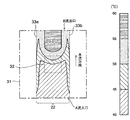
第1の実施形態の半導体装置を説明する前に、MCM(Multi Chip Module)構造を有する関連技術の半導体装置の問題点について説明する。
第2の実施形態では、半導体素子を冷却するための冷却水を流す冷却流路をインターポーザに形成する半導体装置について説明する。
Claims (5)
- シリコン基板、ガラス基板、及びシリコン基板とガラス基板とが接合された基板のいずれかの下側基板と、
前記下側基板に形成され、その上面から下面まで貫通する貫通電極と、
前記下側基板に形成され、その一端側の側面から他端側の側面まで貫通する冷却流路と、
前記下側基板の上に形成され、前記貫通電極に接続されたビルドアップ配線と
を備えた配線基板と、
前記配線基板の上に実装され、前記ビルドアップ配線に接続された複数の半導体素子と、
前記配線基板の下に実装され、前記貫通電極に接続された下側半導体素子とを有し、
前記配線基板上の前記複数の半導体素子は前記冷却流路に沿って配置されており、前記複数の半導体素子のうち、前記冷却流路の流入側に配置される半導体素子は前記冷却流路の流出側に配置される半導体素子よりも発熱量が小さいことを特徴とする半導体装置。 - 前記冷却流路の流入側に配置される半導体素子はメモリ素子であり、前記冷却流路の流出側に配置される半導体素子はロジック素子であることを特徴とする請求項1に記載の半導体装置。
- 前記複数の半導体素子は3つ以上実装され、前記冷却流路の流入側から流出側にかけて、発熱量の小さい順に配置されることを特徴とする請求項1又は請求項2に記載の半導体装置。
- 前記冷却流路の流入側から流出側にかけて、DRAMチップ、フラッシュメモリチップ、CPUチップが順に配置されることを特徴とする請求項3に記載の半導体装置。
- 前記冷却流路を通過した冷却水は、熱交換器によって冷却されて循環することを特徴とする請求項1乃至4のいずれか一項に記載の半導体装置。
Priority Applications (3)
| Application Number | Priority Date | Filing Date | Title |
|---|---|---|---|
| JP2007207962A JP5009085B2 (ja) | 2007-08-09 | 2007-08-09 | 半導体装置 |
| EP08161413.3A EP2023390B1 (en) | 2007-08-09 | 2008-07-30 | Semiconductor device |
| US12/187,636 US7952191B2 (en) | 2007-08-09 | 2008-08-07 | Semiconductor device |
Applications Claiming Priority (1)
| Application Number | Priority Date | Filing Date | Title |
|---|---|---|---|
| JP2007207962A JP5009085B2 (ja) | 2007-08-09 | 2007-08-09 | 半導体装置 |
Publications (3)
| Publication Number | Publication Date |
|---|---|
| JP2009043978A JP2009043978A (ja) | 2009-02-26 |
| JP2009043978A5 JP2009043978A5 (ja) | 2010-05-13 |
| JP5009085B2 true JP5009085B2 (ja) | 2012-08-22 |
Family
ID=40032686
Family Applications (1)
| Application Number | Title | Priority Date | Filing Date |
|---|---|---|---|
| JP2007207962A Expired - Fee Related JP5009085B2 (ja) | 2007-08-09 | 2007-08-09 | 半導体装置 |
Country Status (3)
| Country | Link |
|---|---|
| US (1) | US7952191B2 (ja) |
| EP (1) | EP2023390B1 (ja) |
| JP (1) | JP5009085B2 (ja) |
Families Citing this family (25)
| Publication number | Priority date | Publication date | Assignee | Title |
|---|---|---|---|---|
| PL2294496T3 (pl) * | 2008-05-21 | 2017-10-31 | Asetek As | Rozdzielacz cieplny karty graficznej |
| JP2011222818A (ja) * | 2010-04-12 | 2011-11-04 | Yokogawa Electric Corp | 半導体デバイスの冷却構造 |
| JP5440440B2 (ja) * | 2010-08-06 | 2014-03-12 | 株式会社デンソー | 電子装置 |
| JP5776340B2 (ja) * | 2011-06-06 | 2015-09-09 | 富士通株式会社 | 液体搬送装置及び該搬送装置を用いた半導体冷却装置 |
| JP5779042B2 (ja) | 2011-08-18 | 2015-09-16 | 新光電気工業株式会社 | 半導体装置 |
| DE112012003759T5 (de) * | 2011-09-09 | 2014-09-18 | Ngk Spark Plug Co., Ltd. | Halbleitermodul, Schaltungs-Substrat |
| US9082633B2 (en) * | 2011-10-13 | 2015-07-14 | Xilinx, Inc. | Multi-die integrated circuit structure with heat sink |
| JP5891707B2 (ja) * | 2011-10-28 | 2016-03-23 | 富士通株式会社 | 半導体装置とその製造方法 |
| JP5898919B2 (ja) | 2011-10-31 | 2016-04-06 | 新光電気工業株式会社 | 半導体装置 |
| US9237678B2 (en) * | 2011-11-16 | 2016-01-12 | Toyota Jidosha Kabushiki Kaisha | Cooling device that uses three fluids to cool electronics |
| US8796829B2 (en) | 2012-09-21 | 2014-08-05 | Taiwan Semiconductor Manufacturing Company, Ltd. | Thermal dissipation through seal rings in 3DIC structure |
| US9490190B2 (en) | 2012-09-21 | 2016-11-08 | Taiwan Semiconductor Manufacturing Company, Ltd. | Thermal dissipation through seal rings in 3DIC structure |
| JP6196815B2 (ja) * | 2013-06-05 | 2017-09-13 | 新光電気工業株式会社 | 冷却装置及び半導体装置 |
| JP2015065335A (ja) * | 2013-09-25 | 2015-04-09 | Necプラットフォームズ株式会社 | 電子装置 |
| US9425125B2 (en) * | 2014-02-20 | 2016-08-23 | Altera Corporation | Silicon-glass hybrid interposer circuitry |
| CN106604618B (zh) * | 2017-01-05 | 2024-01-09 | 中国科学院广州能源研究所 | 一种用于数据中心的液冷、风冷复合冷却装置 |
| US10128199B1 (en) * | 2017-07-17 | 2018-11-13 | International Business Machines Corporation | Interchip backside connection |
| CN109950250B (zh) | 2017-12-20 | 2022-03-01 | 晟碟信息科技(上海)有限公司 | 具有矩阵冷却的数据中心3d固态驱动 |
| JP7172471B2 (ja) * | 2018-11-09 | 2022-11-16 | 住友電装株式会社 | 基板構造体 |
| US10763186B2 (en) * | 2018-12-31 | 2020-09-01 | Micron Technology, Inc. | Package cooling by coil cavity |
| US11393807B2 (en) | 2020-03-11 | 2022-07-19 | Peter C. Salmon | Densely packed electronic systems |
| US10966338B1 (en) | 2020-03-11 | 2021-03-30 | Peter C. Salmon | Densely packed electronic systems |
| US11546991B2 (en) | 2020-03-11 | 2023-01-03 | Peter C. Salmon | Densely packed electronic systems |
| US11523543B1 (en) | 2022-02-25 | 2022-12-06 | Peter C. Salmon | Water cooled server |
| US11445640B1 (en) | 2022-02-25 | 2022-09-13 | Peter C. Salmon | Water cooled server |
Family Cites Families (16)
| Publication number | Priority date | Publication date | Assignee | Title |
|---|---|---|---|---|
| US4649990A (en) * | 1985-05-06 | 1987-03-17 | Hitachi, Ltd. | Heat-conducting cooling module |
| JPH05136305A (ja) * | 1991-11-08 | 1993-06-01 | Hitachi Ltd | 発熱体の冷却装置 |
| US6213195B1 (en) * | 1998-12-23 | 2001-04-10 | Hamilton Sundstrand Corporation | Modular coolant manifold for use with power electronics devices having integrated coolers |
| JP2001015675A (ja) * | 1999-06-29 | 2001-01-19 | Hitachi Ltd | マルチチップモジュール |
| JP3518434B2 (ja) * | 1999-08-11 | 2004-04-12 | 株式会社日立製作所 | マルチチップモジュールの冷却装置 |
| US6366462B1 (en) * | 2000-07-18 | 2002-04-02 | International Business Machines Corporation | Electronic module with integral refrigerant evaporator assembly and control system therefore |
| US6822170B2 (en) * | 2000-12-26 | 2004-11-23 | Ngk Spark Plug Co., Ltd. | Embedding resin and wiring substrate using the same |
| CN1284082C (zh) * | 2001-01-19 | 2006-11-08 | 株式会社日立制作所 | 电子电路装置 |
| JP3815239B2 (ja) * | 2001-03-13 | 2006-08-30 | 日本電気株式会社 | 半導体素子の実装構造及びプリント配線基板 |
| JP4604398B2 (ja) * | 2001-06-11 | 2011-01-05 | ソニー株式会社 | 高周波モジュール用基板装置、高周波モジュール装置及びこれらの製造方法 |
| US6433413B1 (en) * | 2001-08-17 | 2002-08-13 | Micron Technology, Inc. | Three-dimensional multichip module |
| JP2004228521A (ja) * | 2003-01-27 | 2004-08-12 | Ngk Spark Plug Co Ltd | 配線基板およびその製造方法 |
| US7019971B2 (en) * | 2003-09-30 | 2006-03-28 | Intel Corporation | Thermal management systems for micro-components |
| JP2005228237A (ja) * | 2004-02-16 | 2005-08-25 | Hitachi Ltd | 液冷システム及びそれを備えた電子機器 |
| JP2007073668A (ja) * | 2005-09-06 | 2007-03-22 | Fujitsu Ltd | 熱を伝える熱伝熱装置、及びこの伝熱装置を実装した電子装置 |
| US7675163B2 (en) * | 2007-03-21 | 2010-03-09 | Sun Microsystems, Inc. | Carbon nanotubes for active direct and indirect cooling of electronics device |
-
2007
- 2007-08-09 JP JP2007207962A patent/JP5009085B2/ja not_active Expired - Fee Related
-
2008
- 2008-07-30 EP EP08161413.3A patent/EP2023390B1/en not_active Ceased
- 2008-08-07 US US12/187,636 patent/US7952191B2/en not_active Expired - Fee Related
Also Published As
| Publication number | Publication date |
|---|---|
| US20090040715A1 (en) | 2009-02-12 |
| EP2023390A1 (en) | 2009-02-11 |
| US7952191B2 (en) | 2011-05-31 |
| EP2023390B1 (en) | 2015-09-23 |
| JP2009043978A (ja) | 2009-02-26 |
Similar Documents
| Publication | Publication Date | Title |
|---|---|---|
| JP5009085B2 (ja) | 半導体装置 | |
| US6670699B2 (en) | Semiconductor device packaging structure | |
| JP5779042B2 (ja) | 半導体装置 | |
| JP2010161184A (ja) | 半導体装置 | |
| US11282812B2 (en) | Thermal management solutions for stacked integrated circuit devices using jumping drops vapor chambers | |
| US7633752B2 (en) | Cooling an integrated circuit die with coolant flow in a microchannel and a thin film thermoelectric cooling device in the microchannel | |
| TWI309549B (en) | Printed circuit board with improved thermal dissipating structure and electronic device with the same | |
| TWI557858B (zh) | 用於積體電路(ic)晶片之散熱結構 | |
| WO2010050087A1 (ja) | 積層型半導体装置及びその製造方法 | |
| JP2008060172A (ja) | 半導体装置 | |
| JP6083516B2 (ja) | マイクロチャネル熱交換装置及び電子機器 | |
| CN213752684U (zh) | 具有竖直热管理的堆叠式硅封装组件 | |
| US11234343B2 (en) | Thermal management solutions for stacked integrated circuit devices using unidirectional heat transfer devices | |
| JP2023507050A (ja) | 積層ボトムダイの冷却を改善する熱伝導スラグ/アクティブダイ | |
| WO2019245684A1 (en) | Thermal management solutions for stacked integrated circuit devices using jumping drops vapor chambers | |
| US20190393192A1 (en) | Thermal management solutions for stacked integrated circuit devices using jumping drops vapor chambers | |
| KR101477309B1 (ko) | 반도체 장치 | |
| JP4997954B2 (ja) | 回路基板、その製造方法及び半導体装置 | |
| JP4817796B2 (ja) | 半導体装置及びその製造方法 | |
| TWI269414B (en) | Package substrate with improved structure for thermal dissipation and electronic device using the same | |
| JP2010251427A (ja) | 半導体モジュール | |
| JPWO2007057952A1 (ja) | 電子素子、それを有するパッケージ及び電子装置 | |
| JP7236930B2 (ja) | 放熱装置 | |
| JP2011205018A (ja) | 半導体パッケージ及び半導体装置 | |
| TWI763569B (zh) | 電子裝置 |
Legal Events
| Date | Code | Title | Description |
|---|---|---|---|
| A521 | Request for written amendment filed |
Free format text: JAPANESE INTERMEDIATE CODE: A523 Effective date: 20100325 |
|
| A621 | Written request for application examination |
Free format text: JAPANESE INTERMEDIATE CODE: A621 Effective date: 20100325 |
|
| A977 | Report on retrieval |
Free format text: JAPANESE INTERMEDIATE CODE: A971007 Effective date: 20111213 |
|
| A131 | Notification of reasons for refusal |
Free format text: JAPANESE INTERMEDIATE CODE: A131 Effective date: 20111220 |
|
| A521 | Request for written amendment filed |
Free format text: JAPANESE INTERMEDIATE CODE: A523 Effective date: 20120201 |
|
| TRDD | Decision of grant or rejection written | ||
| A01 | Written decision to grant a patent or to grant a registration (utility model) |
Free format text: JAPANESE INTERMEDIATE CODE: A01 Effective date: 20120529 |
|
| A01 | Written decision to grant a patent or to grant a registration (utility model) |
Free format text: JAPANESE INTERMEDIATE CODE: A01 |
|
| A61 | First payment of annual fees (during grant procedure) |
Free format text: JAPANESE INTERMEDIATE CODE: A61 Effective date: 20120530 |
|
| R150 | Certificate of patent or registration of utility model |
Ref document number: 5009085 Country of ref document: JP Free format text: JAPANESE INTERMEDIATE CODE: R150 Free format text: JAPANESE INTERMEDIATE CODE: R150 |
|
| FPAY | Renewal fee payment (event date is renewal date of database) |
Free format text: PAYMENT UNTIL: 20150608 Year of fee payment: 3 |
|
| LAPS | Cancellation because of no payment of annual fees |