JP5009085B2 - Semiconductor device - Google Patents
Semiconductor device Download PDFInfo
- Publication number
- JP5009085B2 JP5009085B2 JP2007207962A JP2007207962A JP5009085B2 JP 5009085 B2 JP5009085 B2 JP 5009085B2 JP 2007207962 A JP2007207962 A JP 2007207962A JP 2007207962 A JP2007207962 A JP 2007207962A JP 5009085 B2 JP5009085 B2 JP 5009085B2
- Authority
- JP
- Japan
- Prior art keywords
- heat
- cooling
- semiconductor
- flow path
- semiconductor device
- Prior art date
- Legal status (The legal status is an assumption and is not a legal conclusion. Google has not performed a legal analysis and makes no representation as to the accuracy of the status listed.)
- Expired - Fee Related
Links
Images


Classifications
-
- H—ELECTRICITY
- H01—ELECTRIC ELEMENTS
- H01L—SEMICONDUCTOR DEVICES NOT COVERED BY CLASS H10
- H01L23/00—Details of semiconductor or other solid state devices
- H01L23/34—Arrangements for cooling, heating, ventilating or temperature compensation ; Temperature sensing arrangements
- H01L23/46—Arrangements for cooling, heating, ventilating or temperature compensation ; Temperature sensing arrangements involving the transfer of heat by flowing fluids
- H01L23/473—Arrangements for cooling, heating, ventilating or temperature compensation ; Temperature sensing arrangements involving the transfer of heat by flowing fluids by flowing liquids
-
- H—ELECTRICITY
- H01—ELECTRIC ELEMENTS
- H01L—SEMICONDUCTOR DEVICES NOT COVERED BY CLASS H10
- H01L25/00—Assemblies consisting of a plurality of individual semiconductor or other solid state devices ; Multistep manufacturing processes thereof
- H01L25/03—Assemblies consisting of a plurality of individual semiconductor or other solid state devices ; Multistep manufacturing processes thereof all the devices being of a type provided for in the same subgroup of groups H01L27/00 - H01L33/00, or in a single subclass of H10K, H10N, e.g. assemblies of rectifier diodes
- H01L25/04—Assemblies consisting of a plurality of individual semiconductor or other solid state devices ; Multistep manufacturing processes thereof all the devices being of a type provided for in the same subgroup of groups H01L27/00 - H01L33/00, or in a single subclass of H10K, H10N, e.g. assemblies of rectifier diodes the devices not having separate containers
- H01L25/065—Assemblies consisting of a plurality of individual semiconductor or other solid state devices ; Multistep manufacturing processes thereof all the devices being of a type provided for in the same subgroup of groups H01L27/00 - H01L33/00, or in a single subclass of H10K, H10N, e.g. assemblies of rectifier diodes the devices not having separate containers the devices being of a type provided for in group H01L27/00
- H01L25/0655—Assemblies consisting of a plurality of individual semiconductor or other solid state devices ; Multistep manufacturing processes thereof all the devices being of a type provided for in the same subgroup of groups H01L27/00 - H01L33/00, or in a single subclass of H10K, H10N, e.g. assemblies of rectifier diodes the devices not having separate containers the devices being of a type provided for in group H01L27/00 the devices being arranged next to each other
-
- H—ELECTRICITY
- H01—ELECTRIC ELEMENTS
- H01L—SEMICONDUCTOR DEVICES NOT COVERED BY CLASS H10
- H01L2224/00—Indexing scheme for arrangements for connecting or disconnecting semiconductor or solid-state bodies and methods related thereto as covered by H01L24/00
- H01L2224/01—Means for bonding being attached to, or being formed on, the surface to be connected, e.g. chip-to-package, die-attach, "first-level" interconnects; Manufacturing methods related thereto
- H01L2224/10—Bump connectors; Manufacturing methods related thereto
- H01L2224/15—Structure, shape, material or disposition of the bump connectors after the connecting process
- H01L2224/16—Structure, shape, material or disposition of the bump connectors after the connecting process of an individual bump connector
- H01L2224/161—Disposition
- H01L2224/16151—Disposition the bump connector connecting between a semiconductor or solid-state body and an item not being a semiconductor or solid-state body, e.g. chip-to-substrate, chip-to-passive
- H01L2224/16221—Disposition the bump connector connecting between a semiconductor or solid-state body and an item not being a semiconductor or solid-state body, e.g. chip-to-substrate, chip-to-passive the body and the item being stacked
- H01L2224/16225—Disposition the bump connector connecting between a semiconductor or solid-state body and an item not being a semiconductor or solid-state body, e.g. chip-to-substrate, chip-to-passive the body and the item being stacked the item being non-metallic, e.g. insulating substrate with or without metallisation
- H01L2224/16227—Disposition the bump connector connecting between a semiconductor or solid-state body and an item not being a semiconductor or solid-state body, e.g. chip-to-substrate, chip-to-passive the body and the item being stacked the item being non-metallic, e.g. insulating substrate with or without metallisation the bump connector connecting to a bond pad of the item
-
- H—ELECTRICITY
- H01—ELECTRIC ELEMENTS
- H01L—SEMICONDUCTOR DEVICES NOT COVERED BY CLASS H10
- H01L2224/00—Indexing scheme for arrangements for connecting or disconnecting semiconductor or solid-state bodies and methods related thereto as covered by H01L24/00
- H01L2224/01—Means for bonding being attached to, or being formed on, the surface to be connected, e.g. chip-to-package, die-attach, "first-level" interconnects; Manufacturing methods related thereto
- H01L2224/10—Bump connectors; Manufacturing methods related thereto
- H01L2224/15—Structure, shape, material or disposition of the bump connectors after the connecting process
- H01L2224/16—Structure, shape, material or disposition of the bump connectors after the connecting process of an individual bump connector
- H01L2224/161—Disposition
- H01L2224/16151—Disposition the bump connector connecting between a semiconductor or solid-state body and an item not being a semiconductor or solid-state body, e.g. chip-to-substrate, chip-to-passive
- H01L2224/16221—Disposition the bump connector connecting between a semiconductor or solid-state body and an item not being a semiconductor or solid-state body, e.g. chip-to-substrate, chip-to-passive the body and the item being stacked
- H01L2224/16225—Disposition the bump connector connecting between a semiconductor or solid-state body and an item not being a semiconductor or solid-state body, e.g. chip-to-substrate, chip-to-passive the body and the item being stacked the item being non-metallic, e.g. insulating substrate with or without metallisation
- H01L2224/16235—Disposition the bump connector connecting between a semiconductor or solid-state body and an item not being a semiconductor or solid-state body, e.g. chip-to-substrate, chip-to-passive the body and the item being stacked the item being non-metallic, e.g. insulating substrate with or without metallisation the bump connector connecting to a via metallisation of the item
-
- H—ELECTRICITY
- H01—ELECTRIC ELEMENTS
- H01L—SEMICONDUCTOR DEVICES NOT COVERED BY CLASS H10
- H01L2224/00—Indexing scheme for arrangements for connecting or disconnecting semiconductor or solid-state bodies and methods related thereto as covered by H01L24/00
- H01L2224/01—Means for bonding being attached to, or being formed on, the surface to be connected, e.g. chip-to-package, die-attach, "first-level" interconnects; Manufacturing methods related thereto
- H01L2224/26—Layer connectors, e.g. plate connectors, solder or adhesive layers; Manufacturing methods related thereto
- H01L2224/31—Structure, shape, material or disposition of the layer connectors after the connecting process
- H01L2224/32—Structure, shape, material or disposition of the layer connectors after the connecting process of an individual layer connector
- H01L2224/321—Disposition
- H01L2224/32151—Disposition the layer connector connecting between a semiconductor or solid-state body and an item not being a semiconductor or solid-state body, e.g. chip-to-substrate, chip-to-passive
- H01L2224/32221—Disposition the layer connector connecting between a semiconductor or solid-state body and an item not being a semiconductor or solid-state body, e.g. chip-to-substrate, chip-to-passive the body and the item being stacked
- H01L2224/32225—Disposition the layer connector connecting between a semiconductor or solid-state body and an item not being a semiconductor or solid-state body, e.g. chip-to-substrate, chip-to-passive the body and the item being stacked the item being non-metallic, e.g. insulating substrate with or without metallisation
-
- H—ELECTRICITY
- H01—ELECTRIC ELEMENTS
- H01L—SEMICONDUCTOR DEVICES NOT COVERED BY CLASS H10
- H01L2224/00—Indexing scheme for arrangements for connecting or disconnecting semiconductor or solid-state bodies and methods related thereto as covered by H01L24/00
- H01L2224/01—Means for bonding being attached to, or being formed on, the surface to be connected, e.g. chip-to-package, die-attach, "first-level" interconnects; Manufacturing methods related thereto
- H01L2224/26—Layer connectors, e.g. plate connectors, solder or adhesive layers; Manufacturing methods related thereto
- H01L2224/31—Structure, shape, material or disposition of the layer connectors after the connecting process
- H01L2224/32—Structure, shape, material or disposition of the layer connectors after the connecting process of an individual layer connector
- H01L2224/321—Disposition
- H01L2224/32151—Disposition the layer connector connecting between a semiconductor or solid-state body and an item not being a semiconductor or solid-state body, e.g. chip-to-substrate, chip-to-passive
- H01L2224/32221—Disposition the layer connector connecting between a semiconductor or solid-state body and an item not being a semiconductor or solid-state body, e.g. chip-to-substrate, chip-to-passive the body and the item being stacked
- H01L2224/32245—Disposition the layer connector connecting between a semiconductor or solid-state body and an item not being a semiconductor or solid-state body, e.g. chip-to-substrate, chip-to-passive the body and the item being stacked the item being metallic
-
- H—ELECTRICITY
- H01—ELECTRIC ELEMENTS
- H01L—SEMICONDUCTOR DEVICES NOT COVERED BY CLASS H10
- H01L2224/00—Indexing scheme for arrangements for connecting or disconnecting semiconductor or solid-state bodies and methods related thereto as covered by H01L24/00
- H01L2224/73—Means for bonding being of different types provided for in two or more of groups H01L2224/10, H01L2224/18, H01L2224/26, H01L2224/34, H01L2224/42, H01L2224/50, H01L2224/63, H01L2224/71
- H01L2224/732—Location after the connecting process
- H01L2224/73201—Location after the connecting process on the same surface
- H01L2224/73203—Bump and layer connectors
- H01L2224/73204—Bump and layer connectors the bump connector being embedded into the layer connector
-
- H—ELECTRICITY
- H01—ELECTRIC ELEMENTS
- H01L—SEMICONDUCTOR DEVICES NOT COVERED BY CLASS H10
- H01L2224/00—Indexing scheme for arrangements for connecting or disconnecting semiconductor or solid-state bodies and methods related thereto as covered by H01L24/00
- H01L2224/73—Means for bonding being of different types provided for in two or more of groups H01L2224/10, H01L2224/18, H01L2224/26, H01L2224/34, H01L2224/42, H01L2224/50, H01L2224/63, H01L2224/71
- H01L2224/732—Location after the connecting process
- H01L2224/73251—Location after the connecting process on different surfaces
- H01L2224/73253—Bump and layer connectors
-
- H—ELECTRICITY
- H01—ELECTRIC ELEMENTS
- H01L—SEMICONDUCTOR DEVICES NOT COVERED BY CLASS H10
- H01L2924/00—Indexing scheme for arrangements or methods for connecting or disconnecting semiconductor or solid-state bodies as covered by H01L24/00
- H01L2924/15—Details of package parts other than the semiconductor or other solid state devices to be connected
- H01L2924/151—Die mounting substrate
- H01L2924/153—Connection portion
- H01L2924/1531—Connection portion the connection portion being formed only on the surface of the substrate opposite to the die mounting surface
- H01L2924/15311—Connection portion the connection portion being formed only on the surface of the substrate opposite to the die mounting surface being a ball array, e.g. BGA
-
- H—ELECTRICITY
- H01—ELECTRIC ELEMENTS
- H01L—SEMICONDUCTOR DEVICES NOT COVERED BY CLASS H10
- H01L2924/00—Indexing scheme for arrangements or methods for connecting or disconnecting semiconductor or solid-state bodies as covered by H01L24/00
- H01L2924/15—Details of package parts other than the semiconductor or other solid state devices to be connected
- H01L2924/161—Cap
- H01L2924/1615—Shape
- H01L2924/16152—Cap comprising a cavity for hosting the device, e.g. U-shaped cap
-
- H—ELECTRICITY
- H01—ELECTRIC ELEMENTS
- H01L—SEMICONDUCTOR DEVICES NOT COVERED BY CLASS H10
- H01L2924/00—Indexing scheme for arrangements or methods for connecting or disconnecting semiconductor or solid-state bodies as covered by H01L24/00
- H01L2924/15—Details of package parts other than the semiconductor or other solid state devices to be connected
- H01L2924/161—Cap
- H01L2924/162—Disposition
- H01L2924/16251—Connecting to an item not being a semiconductor or solid-state body, e.g. cap-to-substrate
Landscapes
- Engineering & Computer Science (AREA)
- Power Engineering (AREA)
- Microelectronics & Electronic Packaging (AREA)
- Physics & Mathematics (AREA)
- Condensed Matter Physics & Semiconductors (AREA)
- General Physics & Mathematics (AREA)
- Computer Hardware Design (AREA)
- Cooling Or The Like Of Semiconductors Or Solid State Devices (AREA)
Description
本発明は、半導体装置に関し、特に、半導体素子の温度上昇を抑制する冷却機構を備えた複数の半導体素子が実装される半導体装置に関する。 The present invention relates to a semiconductor device, and more particularly to a semiconductor device on which a plurality of semiconductor elements including a cooling mechanism that suppresses a temperature rise of a semiconductor element is mounted.
従来、電子機器の高性能化・小型化を図るため、配線基板の上に複数の半導体素子を実装して構成されるマルチチップモジュール(MCM)やスタックパッケージなどの半導体装置が開発されている。 2. Description of the Related Art Conventionally, semiconductor devices such as a multichip module (MCM) and a stack package that are configured by mounting a plurality of semiconductor elements on a wiring board have been developed in order to improve the performance and size of electronic devices.
そのような半導体装置では、放熱性を向上させるために、ヒートシンクに代表される放熱板やファンを取り付けて半導体素子を冷却するようにしている。 In such a semiconductor device, in order to improve heat dissipation, a heat sink or a fan represented by a heat sink is attached to cool the semiconductor element.
このような冷却機構に関連する技術として、特許文献1には、半導体素子の上方に設けた流路に冷却水を流して冷却するマルチチップモジュールが開示されており、発熱特性の異なる複数の半導体素子の温度を一様に効率良く冷却するために半導体素子の発熱量に基づいて放熱板の厚さを変えた冷却機構が記載されている。
上記したような半導体装置では、ロジック素子やASICなどの消費電力の大きな半導体素子とDRAMなどの熱に弱い半導体素子が混載されることがある。一般的に、複数の半導体素子は一つの放熱板にその熱が拡散されるように実装される。このため、発熱量の大きな半導体素子は効率よく冷却されるが、その熱が放熱板を介して熱に弱い半導体素子に逆に伝導し、その半導体素子の温度が上昇して誤動作や熱破壊が起こることがある。 In the semiconductor device as described above, a semiconductor element having a large power consumption such as a logic element or ASIC and a heat-sensitive semiconductor element such as a DRAM may be mixed. Generally, a plurality of semiconductor elements are mounted on a single heat sink so that the heat is diffused. For this reason, a semiconductor element with a large amount of heat generation is efficiently cooled, but its heat is conducted back to the heat-sensitive semiconductor element through the heat sink, and the temperature of the semiconductor element rises to cause malfunction or thermal destruction. May happen.
本発明は以上の問題点を鑑みて創作されたものであり、発熱特性の異なる複数の半導体素子が実装される場合であっても、複数の半導体素子を効率よく冷却できる半導体装置を提供することを目的とする。 The present invention was created in view of the above problems, and provides a semiconductor device capable of efficiently cooling a plurality of semiconductor elements even when a plurality of semiconductor elements having different heat generation characteristics are mounted. With the goal.
上記課題を解決するために、シリコン基板、ガラス基板、及びシリコン基板とガラス基板とが接合された基板のいずれかの下側基板と、前記下側基板に形成され、その上面から下面まで貫通する貫通電極と、前記下側基板に形成され、その一端側の側面から他端側の側面まで貫通する冷却流路と、前記下側基板の上に形成され、前記貫通電極に接続されたビルドアップ配線とを備えた配線基板と、前記配線基板の上に実装され、前記ビルドアップ配線に接続された複数の半導体素子と、前記配線基板の下に実装され、前記貫通電極に接続された下側半導体素子とを有し、前記配線基板上の前記複数の半導体素子は前記冷却流路に沿って配置されており、前記複数の半導体素子のうち、前記冷却流路の流入側に配置される半導体素子は前記冷却流路の流出側に配置される半導体素子よりも発熱量が小さいことを特徴とする半導体装置が提供される。 In order to solve the above-described problems, a silicon substrate, a glass substrate, and a lower substrate of any one of a substrate in which a silicon substrate and a glass substrate are bonded to each other, and the lower substrate are formed and penetrate from the upper surface to the lower surface. A through-electrode, a cooling channel formed on the lower substrate and penetrating from a side surface on one end side to a side surface on the other end side, and a buildup formed on the lower substrate and connected to the through-electrode A wiring board comprising wiring, a plurality of semiconductor elements mounted on the wiring board and connected to the build-up wiring, and a lower side mounted below the wiring board and connected to the through electrode A plurality of semiconductor elements on the wiring board are disposed along the cooling flow path, and of the plurality of semiconductor elements, the semiconductor is disposed on the inflow side of the cooling flow path. The element is cooled Wherein a heating value than the semiconductor element arranged on the outflow side of the road is small is provided.
上記課題を解決するために、配線基板に対して水平方向に水を流すための冷却流路を備えた前記配線基板と、前記配線基板の上に実装された複数の半導体素子とを有し、前記配線基板は、シリコン基板、ガラス基板、又はシリコン基板とガラス基板とが接合された貫通電極が設けられた基板の上にビルドアップ配線が設けられて構成され、前記複数の半導体素子は前記冷却流路に沿って配置されており、前記複数の半導体素子のうち、前記冷却流路の流入側に配置される半導体素子は前記冷却流路の流出側に配置される半導体素子よりも発熱量が小さいことを特徴とする半導体装置が提供される。 In order to solve the above problems, the wiring board having a cooling flow path for flowing water in a horizontal direction with respect to the wiring board, and a plurality of semiconductor elements mounted on the wiring board, The wiring substrate is configured by providing a build-up wiring on a silicon substrate, a glass substrate, or a substrate provided with a through electrode in which the silicon substrate and the glass substrate are bonded, and the plurality of semiconductor elements are formed of the cooling substrate. Among the plurality of semiconductor elements, the semiconductor element arranged on the inflow side of the cooling channel has a calorific value more than that of the semiconductor element arranged on the outflow side of the cooling channel. A small semiconductor device is provided.
また、上記形態の半導体装置において、前記複数の半導体素子は、前記配線基板の上側又は下側の少なくとも一方に実装されるようにしてもよい。 In the semiconductor device of the above aspect, the plurality of semiconductor elements may be mounted on at least one of an upper side or a lower side of the wiring board.
本発明の半導体装置では、貫通電極が設けられた基板の上にビルドアップ配線が設けられて構成されるインターポーザに冷却流路を設けている。そして、半導体素子のうち、発熱量が小さく熱に弱い半導体素子を冷却流路の流入口側に配置し、発熱量が大きく熱に強い半導体素子を冷却流路の流出口側に配置している。 In the semiconductor device of the present invention, the cooling channel is provided in the interposer configured by providing the build-up wiring on the substrate on which the through electrode is provided. Of the semiconductor elements, a semiconductor element that generates a small amount of heat and is weak against heat is disposed on the inlet side of the cooling channel, and a semiconductor element that generates a large amount of heat and is resistant to heat is disposed on the outlet side of the cooling channel. .
本発明では、冷却流路を備えた半導体装置において、発熱量が小さく熱に弱い半導体素子と発熱量が大きく熱に強い半導体素子が効率良く冷却されるように工夫されている。冷却流路に流れる水の温度は、冷却流路の流入口側の温度が低く、流出口側の温度が高くなるように分布する。この現象を利用して、熱に弱い半導体素子を流入口側に配置することにより、その半導体素子の温度を集中的に下げることが可能となる。これにより、熱に弱い半導体素子の熱による誤動作を防止して、長期間安定して動作させることが可能となる。 In the present invention, a semiconductor device having a cooling channel is devised so that a semiconductor element having a small heat generation amount and weak against heat and a semiconductor element having a large heat generation amount and strong against heat can be efficiently cooled. The temperature of the water flowing in the cooling channel is distributed so that the temperature on the inlet side of the cooling channel is low and the temperature on the outlet side is high. By utilizing this phenomenon and disposing a heat-sensitive semiconductor element on the inflow side, the temperature of the semiconductor element can be reduced intensively. As a result, it is possible to prevent a malfunction due to heat of a semiconductor element that is vulnerable to heat, and to operate stably for a long period of time.
また、インターポーザの上側だけでなく、下側にも半導体素子が実装される場合には、インターポーザの上下両側に実装される半導体素子を同時に冷却することができる。 When semiconductor elements are mounted not only on the upper side of the interposer but also on the lower side, the semiconductor elements mounted on both the upper and lower sides of the interposer can be cooled at the same time.
以上説明したように、本発明の半導体装置では、発熱特性の異なる複数の半導体素子を実装して構成される半導体装置において、熱に弱い半導体素子を集中的に冷却することができる。 As described above, in the semiconductor device of the present invention, in a semiconductor device configured by mounting a plurality of semiconductor elements having different heat generation characteristics, semiconductor elements that are vulnerable to heat can be intensively cooled.
以下、本発明の実施の形態について、図面を参照しながら説明する。 Hereinafter, embodiments of the present invention will be described with reference to the drawings.
(1)第1の実施形態
第1の実施形態の半導体装置を説明する前に、MCM(Multi Chip Module)構造を有する関連技術の半導体装置の問題点について説明する。
(1) First Embodiment Before describing the semiconductor device of the first embodiment, problems of a related-art semiconductor device having an MCM (Multi Chip Module) structure will be described.
図1は、関連技術の半導体装置の構造の一例を示した図である。図1(a)に半導体装置の上面図を示し、図1(b)に図1(a)のI−I線に沿った断面図を示す。 FIG. 1 is a diagram illustrating an example of the structure of a related-art semiconductor device. FIG. 1A is a top view of the semiconductor device, and FIG. 1B is a cross-sectional view taken along the line I-I in FIG.
図1(b)に示すように、関連技術の半導体装置100は、所要のビルドアップ配線(不図示)が設けられた多層配線基板1の上に複数の半導体素子2a,2b,2cが実装され、その上に放熱板6が配置されて基本構成される。
As shown in FIG. 1B, a
各半導体素子2a、2b、2cのバンプ3が多層配線基板1の接続部にフリップチップ接続されている。例えば、半導体素子2a及び2cはDRAM等のメモリ素子であり、半導体素子2bはCPU等のロジック素子である。
The
また、各半導体素子2a、2b、2cと多層配線基板1との間にはアンダーフィル樹脂4が充填されている。また、多層配線基板1の下面には、はんだボールなどからなる外部接続端子9が設けられている。
An
各半導体素子2a,2b,2cの上部及び多層配線基板1の上部には放熱板6が配置されている。放熱板6はヒートスプレッダ6aとヒートシンク6bで構成される。ヒートスプレッダ6aの中央部にはキャビティC1が設けられており、その周縁の突起状接合部6xが多層配線基板1の周縁部に導電性接着剤7によって接合されている。
A
半導体素子2a,2b,2cはヒートスプレッダ6aのキャビティC1内に収容され、それらの上面がヒートスプレッダ6aのキャビティC1の内面に導電性接着剤7によって接合されている。また、ヒートスプレッダ6aの上部に導電性接着剤7によってヒートシンク6bの下面が接合されている。
The
ヒートシンク6bの底面の面積は、ヒートスプレッダ6aの上面の面積よりも広く、ヒートシンク6bの上面側は溝部を構成してヒートシンク6b全体の表面積を広くすることにより熱の放出量を大きくしている。さらにヒートシンク6bの上部にファン8を設けて空冷を施すことで、半導体装置100全体を冷却するようにしている。
The area of the bottom surface of the
上記したように、半導体素子に対する冷却手段としては放熱板やファンが使用されている。半導体装置100に搭載される複数の半導体素子は、一般に、種類の異なる素子が使用され、各半導体素子から発生する発熱量は半導体素子の種類によって異なる。例えば、計算や判断処理を行うCPU等の機能素子は動作時の発熱量が大きく、メモリ素子の発熱量はCPUの発熱量に比較してかなり小さい。
As described above, a heat sink or a fan is used as a cooling means for the semiconductor element. Generally, different types of elements are used as the plurality of semiconductor elements mounted on the
半導体素子2b(CPU)から発生した熱は放熱板6(ヒートスプレッダ6a及びヒートシンク6b)を介して外部に放熱されるが、ヒートスプレッダ6a内にも熱拡散して、隣接する半導体素子2a,2c(DRAM)の上部にも熱が伝わる。その熱はメモリ素子が発する熱よりも高温であり、結果的に半導体素子2a,2c(DRAM)の温度が上昇してしまい、誤動作や熱破壊が起こることがある。CPUは耐熱温度が比較的高いが、メモリ素子の耐熱温度は低いため、メモリ素子の温度上昇は極力避けることが要求される。
The heat generated from the
本願発明者は、半導体装置に実装される半導体素子の耐熱温度が相違することに着目し、熱に弱い半導体素子を熱に強い半導体素子よりも冷却効果を高くすることについて鋭意研究し、半導体素子の配列順序を考慮した水冷方式を使用することで本問題を解決できることを見出した。 The inventor of the present application pays attention to the fact that the heat resistance temperature of the semiconductor element mounted on the semiconductor device is different, and diligently researched to increase the cooling effect of the heat-sensitive semiconductor element than the heat-resistant semiconductor element. It was found that this problem can be solved by using a water cooling system considering the arrangement order of
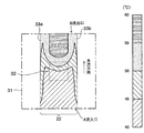
以下に、第1の実施形態における半導体装置について説明する。図2は、第1の実施形態における半導体装置10の構造の一例を示す図である。図2(a)は半導体装置10の上面図を示し、図2(b)は、図2(a)のII−II線に沿った断面図を示す。
The semiconductor device according to the first embodiment will be described below. FIG. 2 is a diagram illustrating an example of the structure of the
図2(b)に示すように、第1の実施形態の半導体装置10では、3層のビルドアップ配線層が形成された多層配線基板11の上に3つの半導体素子17a,17b,17cが実装され、その上部に放熱板21が配置されて基本構成されている。
As shown in FIG. 2B, in the
多層配線基板11の配線層12a,12b,12cと層間絶縁膜13a,13bは相互に積層されるように形成され、各配線層12a,12b,12cは、層間絶縁膜13a,13bに設けられたビアホール14を介して相互接続されている。多層配線基板11の上部には、配線層12cの接続部上に開口部が設けられたソルダレジスト15が形成されている。そして、半導体素子17a,17b,17cのバンプ18が配線層12cの接続部にフリップチップ接続されている。各半導体素子17a,17b,17cと多層配線基板11との間にはアンダーフィル樹脂19が充填されている。
The wiring layers 12a, 12b and 12c of the
また、多層配線基板11の下面にも配線層12aの接続部に開口部が設けられたソルダレジスト16が形成されている。配線層12aの接続部には、はんだボールを搭載するなどして形成された外部接続端子20が設けられている。
Also, a solder resist 16 having an opening at the connection portion of the
さらに、各半導体素子17a,17b,17cの上部及び多層配線基板11の上部には放熱板21が配置されている。放熱板21は例えば銅(Cu)部材の表面にニッケル(Ni)層がコートされて構成される。放熱板21は、中央部にキャビティC2が設けられることで周縁部に突起状接合部21aが形成されており、その突起状接合部21aが多層配線基板11の周縁部に導電性接着剤23によって接合されている。導電性接着剤23としては、例えば銀ペーストが使用される。さらに、半導体素子17a,17b,17cの上面が導電性接着剤23によって放熱板21のキャビティC2の内面に接合されている。導電性接着剤23を使用することで半導体素子17a,17b,17cに放熱板21を固定するとともに、半導体素子17a,17b,17cから発生する熱を逃がすようにしている。
Further, a
このようにして、放熱板21のキャビティC2の内部に半導体素子17a,17b,17cが収容されて実装されている。
In this manner, the
多層配線基板11の上部には複数の半導体素子(図2(b)の例では3つ)が一列に実装されている。このうち半導体素子17aはCPU等のロジック素子であって熱に強く、発熱量が大きい。発熱量の大きな半導体素子17aとしては、CPUの他に、ASIC(ローパワーCPU)などのロジック素子がある。
A plurality of semiconductor elements (three in the example of FIG. 2B) are mounted in a row on the
また、半導体素子17bはフラッシュメモリであって、半導体素子17aのロジック素子よりも発熱量が小さい。また、半導体素子17cはDRAMであって、3つの半導体素子17a,17b,17cのうち最も熱に弱く、発熱量が小さい。発熱量の小さな半導体素子17b,17cとしては、フラッシュメモリやDRAMの他に、SRAMやFeRAMなどの各種のメモリ素子が含まれる。
Further, the
これら3つの半導体素子17a,17b,17cは所要の間隔を保って多層配線基板11の上部に配置されている。
These three
さらに、放熱板21には、一列に実装された半導体素子17a,17b,17cの上方に、この列に沿って水平方向に貫通して形成された冷却流路22が設けられている。冷却流路22に冷却水を流すことにより、半導体素子17a,17b,17cを冷却することができる。図2(b)に示した冷却流路22は右側が流入口Aになり左側が流出口Bになる。すなわち、発熱量が小さく熱に弱い半導体素子17cは冷却流路22の流入口A側に配置され、発熱量が大きく熱に強い半導体素子17aは冷却流路22の流出口B側に配置される。このようにして、複数の半導体素子17a,17b,17cが冷却流路22に沿って配置される。
Further, the
図2(a)及び(b)に示すように半導体素子17a,17b,17cを配置して冷却流路22に冷却水を流すことによって、半導体素子を効果的に冷却できることについて以下に説明する。
The following describes how the semiconductor elements can be effectively cooled by arranging the
まず、発熱量の大きな1個の半導体素子(以下、チップともいう)がパッケージの中央に実装されたときに、冷却流路22に冷却水を流して半導体素子を冷却したときの水の温度分布について検討した。図3は温度分布のシミュレーション結果を示している。このシミュレーションでは、チップの発熱量を60Wとし、冷却流路22に流入する水の温度を40℃とした。
First, when one semiconductor element (hereinafter also referred to as a chip) having a large calorific value is mounted in the center of the package, the temperature distribution of the water when cooling the semiconductor element by flowing cooling water through the
図3の一点鎖線で囲まれた領域はパッケージ31であり、破線で囲まれた領域はパッケージの中央部に実装されたチップ32である。パッケージ31の大きさは40mm□であり、チップ32の大きさは10mm□である。また、破線33a、33bで挟まれた領域は冷却流路22が配置された位置を示している。この冷却流路22は図3の下側が流入口Aとなり上側が流出口Bとなっている。
A region surrounded by a one-dot chain line in FIG. 3 is a
図3に示すように、冷却流路22上の流入口Aからチップ32のほぼ中央部までの領域は水温が40〜45℃(右上がり斜線部)であった。また、チップ32の中央部からその近傍の流出口B側では水温が45〜50℃(右下がり斜線部)から50〜55℃(点ハッチング部)に上昇した。さらに、そこから流出口Bまでの領域では、水温が中央部で55〜60℃(水平斜線部)で、その両端側で50〜55℃(点ハッチング部)であった。このように、流入口Aから流出口B側に近づくにつれて水温が上昇することが確認された。
As shown in FIG. 3, the water temperature in the region from the inlet A on the
図3の結果から明らかなように、高熱を発するチップ32の冷却流路22の流出口B側になるほど水温が上昇する。そのため、冷却流路22の流出口B側に熱に弱いチップを配置すると、高熱によってチップが誤動作したり熱破壊するおそれがある。
As is clear from the results of FIG. 3, the water temperature rises toward the outlet B side of the
次に、発熱量の異なる複数のチップをパッケージに実装した場合の温度シミュレーション結果について説明する。 Next, a temperature simulation result when a plurality of chips having different heat generation amounts are mounted on a package will be described.
図4(a)は、発熱量の大きな1つのチップと発熱量の小さな2つのチップを実装した半導体装置において、空冷または水冷を施したときのチップの温度をシミュレーションにより算出した結果を示している。 FIG. 4A shows the result of calculating the temperature of a chip by air-cooling or water-cooling in a semiconductor device on which one chip with a large amount of heat generation and two chips with a small amount of heat generation are mounted. .
使用する3つのチップのうち、チップ1及びチップ2の発熱量を0.5Wとし、チップ3の発熱量を60Wとしている。これらのチップは水流方向に向けてチップ1、チップ2、チップ3の順に一列に配置されるものとする。
Of the three chips used, the heating value of
図4(a)における空冷は、前述した図1に示した関連技術の半導体装置100を使用する場合であり、チップ1からチップ3の上部を放熱板及びファンにより全体的に冷却する場合である。また、水冷は、第1の実施形態の半導体装置10を使用する場合であり、冷却流路22の流入口A側から流出口B側に、チップ1、チップ2、チップ3の順に配置している。すなわち、発熱量が小さく熱に弱いチップ(チップ1)が冷却流路22の流入口A側に配置され、発熱量が大きく熱に強いチップ(チップ3)が冷却流路22の流出口B側に配置される。
The air cooling in FIG. 4A is a case where the
図4(b)は、上記のようにチップを配置したときのチップの温度(図4(a)のデータ)をグラフ化した図である。破線は比較のため、チップの配置を同様にして図1に示した空冷を施したときのチップの温度を示した図である。 FIG. 4B is a graph showing the chip temperature (data in FIG. 4A) when the chip is arranged as described above. The broken line is a graph showing the temperature of the chip when the air cooling shown in FIG.
図4(a)及び(b)に示すように、チップ1の温度は空冷のときには76.38℃になったのに対し、水冷のときは45.09℃となった。また、チップ2の温度は空冷のときには81.51℃になったのに対し、水冷のときは63.12℃となった。また、チップ3の温度は空冷のときには100.33℃になったのに対し、水冷のときは108.98℃となった。このように、チップ1、チップ2の温度は空冷を施したときよりも温度がかなり低くなり、チップ3の温度は空冷を施したときよりも若干温度が高くなる程度である。
As shown in FIGS. 4A and 4B, the temperature of the
熱に弱いチップ1、チップ2については、第1の実施形態の水冷を施した方が空冷を施したときよりも熱の上昇を抑えることができる。従って、熱に弱いチップは空冷のときよりも、誤動作することなく長時間安定して動作させることが可能となる。
As for the
一方、熱に強いチップ3については、第1の実施形態の水冷を施すと、空冷を施したときよりもチップの温度が若干高くなってしまうものの、熱に強いチップ3は、ある程度の高熱に耐えられるように設計されており、許容範囲内の温度であれば実用上問題が発生しない。
On the other hand, for the
図5は、上記した水冷による冷却機構を備えた半導体装置10を含む全体構成の一例を示す模式図である。
FIG. 5 is a schematic diagram showing an example of the entire configuration including the
図5の半導体装置10の冷却流路22を流れる冷却水は、図5の矢印の方向に循環させて使用される。半導体装置10の右側の流入口Aから流入した冷却水は冷却流路22を左側へ移動するにつれて、半導体素子の発熱により水温が上昇する。この冷却水は冷却流路22の左側の流出口Bから流出し、ラジエータ55(熱交換器)によって所要の温度(例えば40℃)以下に水温が下げられ、タンク53に貯められる。タンク53内の冷却された水はポンプによって半導体装置10に再度送られ、半導体装置10の冷却流路22を通り、半導体素子を冷却する。このようにして冷却水を循環させることにより、冷却水の温度上昇が抑えられて半導体素子が安定して冷却される。
The cooling water flowing through the
以上説明したように第1の実施形態の半導体装置10では、冷却流路22を流れる水の温度の違いを積極的に利用し、水温の低い冷却流路22の流入口A側に熱に弱い半導体素子を配置して、その半導体素子の温度を集中的に下げるようにしている。これにより、熱に弱い半導体素子の温度を集中的に下げることができ、熱に弱い半導体素子が誤動作することなく長期間安定して動作させることが可能になる。また、熱の発生量が大きな半導体素子は耐熱性があるので、比較的温度が高くなる冷却流路22の流出口B側に配置しても十分な性能が得られる程度に冷却される。
As described above, in the
また、第1の実施形態の半導体装置10では、放熱板21に冷却流路22を設け、そこに冷却水を流して半導体素子を冷却しており、空冷式で使用されるサイズの大きなヒートシンクやファンは使用していない。このため、半導体装置10を薄型化、小型化することが可能となる。
Further, in the
なお、上記説明では発熱量の小さな2つのチップと発熱量の大きな1つのチップの3つのチップについて検討した。この検討を基に、3つのチップがそれぞれ異なる発熱量の場合については、冷却流路22の流入口A側から流出口B側に発熱量の小さなチップの順に配置することにより、冷却流路22を流れる水の温度が流入口A側に近いほど低くなり、熱に弱いチップほど集中的に冷却できることがわかる。
In the above description, three chips, that is, two chips with a small amount of heat generation and one chip with a large amount of heat generation were examined. Based on this study, in the case where the three chips have different heat generation amounts, the
また、半導体素子の数が4つ以上の場合にも、冷却流路22の流入口A側から流出口B側の方向に、発熱量が小から大になるようにチップを配置すれば、熱に弱いチップほど集中的に冷却することが可能となる。
Even when the number of semiconductor elements is four or more, if the chip is arranged in the direction from the inlet A side to the outlet B side of the
また、上記説明では、冷却流路22が1本の場合について説明したが、これに限らず、放熱板21に複数の冷却流路22を形成するようにしてもよい。例えば、冷却流路22が水平方向又は上下方向に平行になるように複数形成してもよい。
In the above description, the case where the number of the
上記した第1の実施形態の冷却流路22を備えた放熱板21は以下のようにして形成される。
The
まず、放熱板21を構成する第1の金属板を用意し、第1の金属板に所要のサイズのキャビティを設ける。このキャビティは、金型を使用してプレス加工によって形成してもよいし、ドリル加工やレーザ加工によってキャビティを形成してもよい。次に、第1の金属板のキャビティが形成された面と反対側の面に、所要のサイズの溝を形成する。次に、第2の金属板と溝が形成された第1の金属板とを接合して、冷却流路22を備えた放熱板21を形成する。
First, the 1st metal plate which comprises the
このようにして形成された放熱板と半導体素子が搭載された多層配線基板とを接合することにより、半導体装置が製造される。 The semiconductor device is manufactured by bonding the heat sink formed in this manner and the multilayer wiring board on which the semiconductor element is mounted.
(2)第2の実施形態
第2の実施形態では、半導体素子を冷却するための冷却水を流す冷却流路をインターポーザに形成する半導体装置について説明する。
(2) Second Embodiment In the second embodiment, a semiconductor device is described in which a cooling flow path for flowing cooling water for cooling a semiconductor element is formed in an interposer.
図6(a)〜(c)に冷却流路がインターポーザに形成された半導体装置60の一例を示す。図6(a)は半導体装置の上面図であり、図6(b)はその下面図である。また、図6(c)は、図6(a)の冷却流路64の中心線に沿って貫通電極62の手前側から見た断面図である。
FIGS. 6A to 6C show an example of the
図6(c)に示すように、第2の実施形態の半導体装置60は、冷却流路64が設けられた流路付き配線基板61a及びその上に形成された多層配線部61bからなるインターポーザ61と、インターポーザ61の上下両側に実装された半導体素子68a,68b,69a,69bとによって基本構成される。
As shown in FIG. 6C, the
インターポーザ61の流路付き配線基板61aには、基板5の縦方向に貫通するスルーホールTHが設けられ、その内面にシリコン酸化膜からなる絶縁層57が形成されている。さらに、スルーホールTH内に銅が充填されて貫通電極62が設けられている。貫通電極62は絶縁層57によって他の貫通電極62と電気的に絶縁されている。
The
貫通電極62は、図6(a)及び図6(b)を加えて参照すると、冷却流路64を避けて、その近傍の基板5の両端側に配置されている。冷却流路64の詳細については後述する。
6A and 6B, the through
また、インターポーザ61の下面側には配線層74が設けられ、配線層74の接続部に開口部が設けられたソルダレジスト56が形成されており、半導体素子69a,69bのバンプ72が配線層74にフリップチップ接続されている。インターポーザ61の下面側の半導体素子69a,69bの外側の配線層74にはんだボールなどが搭載されて外部接続端子73が設けられている。
In addition, a
なお、インターポーザ61の基板5は、好適には、シリコン基板(厚さ200〜300μm)が使用される。シリコン基板を使用することにより、微細加工が可能になるので、半導体装置の小型化、薄型化、高性能化などを実現するための高密度実装が可能となる。
The
多層配線部61bはビルドアップ配線から形成され、多層配線部61bの上に半導体素子68a,68bが接続されている。図6(c)の例では基板5の上に3層のビルドアップ配線が形成されている。多層配線部61bの配線層65a,65b,65cと層間絶縁膜66a,66bは相互に積層されるように形成され、各配線層65a,65b,65cは、層間絶縁膜66a,66bに設けられたビアホール59を介して相互接続されている。多層配線部61bの上には、配線層65cの接続部に開口部が設けられたソルダレジスト67が形成されている。そして、半導体素子68a,68bのバンプ71が配線層65cにフリップチップ接続されている。また、半導体素子68a,68bと多層配線部61bとの間にアンダーフィル樹脂70が充填されている。
The
多層配線部61bの配線層65aが貫通電極62の上部と接続され、貫通電極62の下部がインターポーザ61の下面側の配線層74と接続されている。このようにして、貫通電極62によって基板5の上面側の配線層65a〜65cと下面側の配線層74とが相互接続されている。
The
次に、インターポーザ61の流路付き配線基板61aに形成される冷却流路64について説明する。
Next, the
インターポーザ61の流路付き配線基板61aにはインターポーザ61の上部に形成される複数の半導体素子68a,68b又はインターポーザ61の下部に形成される複数の半導体素子69a、69bが一列に配置される方向に貫通孔が形成され、これらの半導体素子68a,68b,69a,69bを冷却するための水の冷却流路64となっている。冷却流路64は図6(a)〜(c)に示すようにインターポーザ61を一端側の側面から対向する他端側の側面まで、水平方向に貫通して設けられる。
In the
図6(a)〜(c)に示した冷却流路64はその右側が流入口Aになり左側が流出口Bになる。このようなインターポーザ61の上部に接続される半導体素子68a、68bのうち熱に弱い半導体素子68b(DRAMなど)は図6(a)〜(c)の右側に配置される。また、インターポーザ61の下部においても、半導体素子69a、69bのうち熱に弱い半導体素子69bは図6の右側に配置される。すなわち、熱に弱い半導体素子68b,69bは冷却流路64の流入口A側に配置され、熱に強い半導体素子68a、69aは冷却流路64の流出口B側に配置される。
The cooling
なお、冷却流路64を通過した冷却水は、前述した図5での説明と同様に、流出口Bから流出した冷却水の水温を所要の温度に下げて、循環して使用される。
Note that the cooling water that has passed through the
以上説明したように、第2の実施形態の半導体装置60では、熱に弱い半導体素子68b,69bを冷却流路64の流入口A側に配置することにより、第1の実施形態で説明した半導体装置10の場合と同様に、熱に弱い半導体素子に対する冷却効果を高めることができる。熱に弱い半導体素子の温度を集中的に下げることにより、熱に弱い半導体素子が誤動作することなく長期間安定して動作させることが可能になる。
As described above, in the
また、インターポーザ61の上下両面に半導体素子を実装した場合には、上記した配置にすることによりインターポーザ61の上面側に接続された熱に弱い半導体素子だけでなく、インターポーザ61の下面側に接続された熱に弱い半導体素子に対しても冷却効果を高めることが可能となる。
In addition, when semiconductor elements are mounted on both the upper and lower surfaces of the
なお、第2の実施形態ではインターポーザ61の基板5としてシリコンを使用する場合について説明したが、シリコンに限らず、例えばガラスを使用してインターポーザ61を形成するようにしてもよい。
In the second embodiment, the case where silicon is used as the
また、図6(c)の半導体装置では、インターポーザ61の上下両面に半導体素子が実装される場合を示しているが、インターポーザ61の片面側のみに半導体素子を実装してもよいことは勿論である。
6C shows a case where semiconductor elements are mounted on both upper and lower surfaces of the
また、図6ではインターポーザ61に冷却流路64が1つ形成された場合を示しているが、これに限らず、冷却流路64が水平方向又は上下方向に平行になるように複数形成してもよい。冷却流路64を水平方向に複数形成する場合には、冷却流路64の間に貫通電極62を配置することも可能となる。
6 shows a case where one
また、第2の実施形態では、インターポーザ61の基板5の内部に冷却流路64を形成して、そこに冷却水を流すことにより半導体素子を冷却するようにしているが、半導体素子に対する冷却効果をさらに高めるために、図6(c)の構成にさらに放熱板を付加するようにしてもよい。インターポーザ61の上面側に配置した半導体素子の上部に放熱板を配置することにより、放熱板の下の熱に弱い半導体素子に対する冷却効果をさらに高めることができる。
In the second embodiment, the cooling
さらに、第1の実施形態と同様に、半導体素子の上に配置された放熱板に冷却流路を設けることも可能である。 Further, similarly to the first embodiment, it is also possible to provide a cooling flow path in the heat radiating plate disposed on the semiconductor element.
なお、インターポーザ61の基板5の冷却流路64は以下のようにして形成される。
The
まず、第1のシリコンウエハを用意し、第1のシリコンウエハにフォトリソグラフィとドライエッチングによって所要のサイズの溝を形成する。次に、第2のシリコンウエハと溝が形成された第1のシリコンウエハとを接着する。この接着はArプラズマ照射後、1000℃でアニールすることにより行う。 First, a first silicon wafer is prepared, and a groove having a required size is formed on the first silicon wafer by photolithography and dry etching. Next, the second silicon wafer is bonded to the first silicon wafer in which the grooves are formed. This adhesion is performed by annealing at 1000 ° C. after Ar plasma irradiation.
また、インターポーザ61の基板5はシリコンに限らず、ガラスを用いてもよい。ガラスを用いる場合には、まず、第1のガラスを用意し、第1のガラスの上に所要の開口部を備えたマスクを形成し、その開口部に露出するガラスの部分をサンドブラスト法などによって加工して所要の溝を形成する。なお、所要の型に熔融したガラスを流し込むことによって、同様な構造にしてもよい。次に、第2のガラスと溝が形成された第1のガラスとを接着する。
The
また、インターポーザ61はシリコンとガラスによって形成するようにしてもよい。上記方法によって所要の溝を形成したシリコンとガラスとを接着する。シリコンとガラスは陽極接合によって接合する。例えば、シリコン及びガラスを300〜400℃に加熱した状態で、両者の間に500V〜1kVの電圧を印加することにより、陽極接合することができる。
The
上記したように冷却流路となる水平方向に貫通する貫通孔を備えた流路付き配線基板61aを形成した後、貫通電極や多層ビルドアップ配線などを形成する。
As described above, after forming the
1,11…多層配線基板、10,60…半導体装置、12,65…配線層、13,66…層間絶縁膜、14,59…ビアホール、16,56,67…ソルダレジスト、17,68,69…半導体素子、18,71…半田バンプ、19,70…アンダーフィル樹脂、20,73…外部接続端子、21…放熱板、22,64…冷却流路、23…導電性接着剤、55…熱交換器、61…インターポーザ、62…貫通電極、C1,C2…キャビティ、TH…スルーホール。
DESCRIPTION OF
Claims (5)
前記下側基板に形成され、その上面から下面まで貫通する貫通電極と、
前記下側基板に形成され、その一端側の側面から他端側の側面まで貫通する冷却流路と、
前記下側基板の上に形成され、前記貫通電極に接続されたビルドアップ配線と
を備えた配線基板と、
前記配線基板の上に実装され、前記ビルドアップ配線に接続された複数の半導体素子と、
前記配線基板の下に実装され、前記貫通電極に接続された下側半導体素子とを有し、
前記配線基板上の前記複数の半導体素子は前記冷却流路に沿って配置されており、前記複数の半導体素子のうち、前記冷却流路の流入側に配置される半導体素子は前記冷却流路の流出側に配置される半導体素子よりも発熱量が小さいことを特徴とする半導体装置。 A lower substrate of any of a silicon substrate, a glass substrate, and a substrate in which the silicon substrate and the glass substrate are bonded;
A through electrode formed on the lower substrate and penetrating from the upper surface to the lower surface;
A cooling channel formed in the lower substrate and penetrating from a side surface on one end side to a side surface on the other end side;
Build-up wiring formed on the lower substrate and connected to the through electrode
A wiring board comprising:
A plurality of semiconductor elements mounted on the wiring board and connected to the build-up wiring;
A lower semiconductor element mounted under the wiring board and connected to the through electrode;
The plurality of semiconductor elements on the wiring substrate are arranged along the cooling flow path, and the semiconductor elements arranged on the inflow side of the cooling flow path among the plurality of semiconductor elements are the cooling flow paths. A semiconductor device characterized in that a calorific value is smaller than that of a semiconductor element arranged on the outflow side.
Priority Applications (3)
| Application Number | Priority Date | Filing Date | Title |
|---|---|---|---|
| JP2007207962A JP5009085B2 (en) | 2007-08-09 | 2007-08-09 | Semiconductor device |
| EP08161413.3A EP2023390B1 (en) | 2007-08-09 | 2008-07-30 | Semiconductor device |
| US12/187,636 US7952191B2 (en) | 2007-08-09 | 2008-08-07 | Semiconductor device |
Applications Claiming Priority (1)
| Application Number | Priority Date | Filing Date | Title |
|---|---|---|---|
| JP2007207962A JP5009085B2 (en) | 2007-08-09 | 2007-08-09 | Semiconductor device |
Publications (3)
| Publication Number | Publication Date |
|---|---|
| JP2009043978A JP2009043978A (en) | 2009-02-26 |
| JP2009043978A5 JP2009043978A5 (en) | 2010-05-13 |
| JP5009085B2 true JP5009085B2 (en) | 2012-08-22 |
Family
ID=40032686
Family Applications (1)
| Application Number | Title | Priority Date | Filing Date |
|---|---|---|---|
| JP2007207962A Expired - Fee Related JP5009085B2 (en) | 2007-08-09 | 2007-08-09 | Semiconductor device |
Country Status (3)
| Country | Link |
|---|---|
| US (1) | US7952191B2 (en) |
| EP (1) | EP2023390B1 (en) |
| JP (1) | JP5009085B2 (en) |
Families Citing this family (25)
| Publication number | Priority date | Publication date | Assignee | Title |
|---|---|---|---|---|
| PL2294496T3 (en) * | 2008-05-21 | 2017-10-31 | Asetek As | Graphics card thermal interposer |
| JP2011222818A (en) * | 2010-04-12 | 2011-11-04 | Yokogawa Electric Corp | Cooling structure for semiconductor device |
| JP5440440B2 (en) * | 2010-08-06 | 2014-03-12 | 株式会社デンソー | Electronic equipment |
| JP5776340B2 (en) * | 2011-06-06 | 2015-09-09 | 富士通株式会社 | Liquid transport device and semiconductor cooling device using the transport device |
| JP5779042B2 (en) | 2011-08-18 | 2015-09-16 | 新光電気工業株式会社 | Semiconductor device |
| CN103782379A (en) * | 2011-09-09 | 2014-05-07 | 日本特殊陶业株式会社 | Semiconductor module, and circuit board |
| US9082633B2 (en) * | 2011-10-13 | 2015-07-14 | Xilinx, Inc. | Multi-die integrated circuit structure with heat sink |
| JP5891707B2 (en) * | 2011-10-28 | 2016-03-23 | 富士通株式会社 | Semiconductor device and manufacturing method thereof |
| JP5898919B2 (en) | 2011-10-31 | 2016-04-06 | 新光電気工業株式会社 | Semiconductor device |
| CN103946043B (en) * | 2011-11-16 | 2016-06-01 | 丰田自动车株式会社 | The chiller of electrical equipment |
| US9490190B2 (en) | 2012-09-21 | 2016-11-08 | Taiwan Semiconductor Manufacturing Company, Ltd. | Thermal dissipation through seal rings in 3DIC structure |
| US8796829B2 (en) | 2012-09-21 | 2014-08-05 | Taiwan Semiconductor Manufacturing Company, Ltd. | Thermal dissipation through seal rings in 3DIC structure |
| JP6196815B2 (en) | 2013-06-05 | 2017-09-13 | 新光電気工業株式会社 | Cooling device and semiconductor device |
| JP2015065335A (en) * | 2013-09-25 | 2015-04-09 | Necプラットフォームズ株式会社 | Electronic apparatus |
| US9425125B2 (en) * | 2014-02-20 | 2016-08-23 | Altera Corporation | Silicon-glass hybrid interposer circuitry |
| CN106604618B (en) * | 2017-01-05 | 2024-01-09 | 中国科学院广州能源研究所 | Liquid cooling and air cooling composite cooling device for data center |
| US10128199B1 (en) * | 2017-07-17 | 2018-11-13 | International Business Machines Corporation | Interchip backside connection |
| CN109950250B (en) | 2017-12-20 | 2022-03-01 | 晟碟信息科技(上海)有限公司 | Data center 3D solid state drive with matrix cooling |
| JP7172471B2 (en) * | 2018-11-09 | 2022-11-16 | 住友電装株式会社 | Substrate structure |
| US10763186B2 (en) * | 2018-12-31 | 2020-09-01 | Micron Technology, Inc. | Package cooling by coil cavity |
| US11393807B2 (en) | 2020-03-11 | 2022-07-19 | Peter C. Salmon | Densely packed electronic systems |
| US11546991B2 (en) | 2020-03-11 | 2023-01-03 | Peter C. Salmon | Densely packed electronic systems |
| US10966338B1 (en) | 2020-03-11 | 2021-03-30 | Peter C. Salmon | Densely packed electronic systems |
| US11523543B1 (en) | 2022-02-25 | 2022-12-06 | Peter C. Salmon | Water cooled server |
| US11445640B1 (en) | 2022-02-25 | 2022-09-13 | Peter C. Salmon | Water cooled server |
Family Cites Families (16)
| Publication number | Priority date | Publication date | Assignee | Title |
|---|---|---|---|---|
| US4649990A (en) * | 1985-05-06 | 1987-03-17 | Hitachi, Ltd. | Heat-conducting cooling module |
| JPH05136305A (en) * | 1991-11-08 | 1993-06-01 | Hitachi Ltd | Cooling device for heating element |
| US6213195B1 (en) * | 1998-12-23 | 2001-04-10 | Hamilton Sundstrand Corporation | Modular coolant manifold for use with power electronics devices having integrated coolers |
| JP2001015675A (en) * | 1999-06-29 | 2001-01-19 | Hitachi Ltd | Multi-chip module |
| JP3518434B2 (en) * | 1999-08-11 | 2004-04-12 | 株式会社日立製作所 | Multi-chip module cooling system |
| US6366462B1 (en) * | 2000-07-18 | 2002-04-02 | International Business Machines Corporation | Electronic module with integral refrigerant evaporator assembly and control system therefore |
| US6822170B2 (en) * | 2000-12-26 | 2004-11-23 | Ngk Spark Plug Co., Ltd. | Embedding resin and wiring substrate using the same |
| US7091598B2 (en) * | 2001-01-19 | 2006-08-15 | Renesas Technology Corporation | Electronic circuit device |
| JP3815239B2 (en) * | 2001-03-13 | 2006-08-30 | 日本電気株式会社 | Semiconductor device mounting structure and printed wiring board |
| JP4604398B2 (en) * | 2001-06-11 | 2011-01-05 | ソニー株式会社 | High frequency module substrate device, high frequency module device and manufacturing method thereof |
| US6433413B1 (en) * | 2001-08-17 | 2002-08-13 | Micron Technology, Inc. | Three-dimensional multichip module |
| JP2004228521A (en) * | 2003-01-27 | 2004-08-12 | Ngk Spark Plug Co Ltd | Wiring board and its manufacturing method |
| US7019971B2 (en) * | 2003-09-30 | 2006-03-28 | Intel Corporation | Thermal management systems for micro-components |
| JP2005228237A (en) * | 2004-02-16 | 2005-08-25 | Hitachi Ltd | Liquid cooled system and electronic equipment provided therewith |
| JP2007073668A (en) * | 2005-09-06 | 2007-03-22 | Fujitsu Ltd | Heat-transfer device for heat conduction, and electronic equipment mounted therewith |
| US7675163B2 (en) * | 2007-03-21 | 2010-03-09 | Sun Microsystems, Inc. | Carbon nanotubes for active direct and indirect cooling of electronics device |
-
2007
- 2007-08-09 JP JP2007207962A patent/JP5009085B2/en not_active Expired - Fee Related
-
2008
- 2008-07-30 EP EP08161413.3A patent/EP2023390B1/en not_active Expired - Fee Related
- 2008-08-07 US US12/187,636 patent/US7952191B2/en not_active Expired - Fee Related
Also Published As
| Publication number | Publication date |
|---|---|
| US7952191B2 (en) | 2011-05-31 |
| US20090040715A1 (en) | 2009-02-12 |
| JP2009043978A (en) | 2009-02-26 |
| EP2023390A1 (en) | 2009-02-11 |
| EP2023390B1 (en) | 2015-09-23 |
Similar Documents
| Publication | Publication Date | Title |
|---|---|---|
| JP5009085B2 (en) | Semiconductor device | |
| US6670699B2 (en) | Semiconductor device packaging structure | |
| JP5779042B2 (en) | Semiconductor device | |
| JP2010161184A (en) | Semiconductor device | |
| US11282812B2 (en) | Thermal management solutions for stacked integrated circuit devices using jumping drops vapor chambers | |
| TWI309549B (en) | Printed circuit board with improved thermal dissipating structure and electronic device with the same | |
| TWI557858B (en) | Design of a heat dissipation structure for an integrated circuit (ic) chip | |
| WO2010050087A1 (en) | Layered semiconductor device and manufacturing method therefor | |
| JP2002151640A (en) | Semiconductor device | |
| JP2008060172A (en) | Semiconductor device | |
| JP6083516B2 (en) | Micro-channel heat exchange device and electronic equipment | |
| CN213752684U (en) | Stacked silicon package with vertical thermal management | |
| US11234343B2 (en) | Thermal management solutions for stacked integrated circuit devices using unidirectional heat transfer devices | |
| JP2023507050A (en) | Thermally conductive slug/active die for improved cooling of stacked bottom die | |
| US20190393192A1 (en) | Thermal management solutions for stacked integrated circuit devices using jumping drops vapor chambers | |
| KR101477309B1 (en) | Semiconductor device | |
| JP4997954B2 (en) | Circuit board, manufacturing method thereof, and semiconductor device | |
| JP4817796B2 (en) | Semiconductor device and manufacturing method thereof | |
| TWI269414B (en) | Package substrate with improved structure for thermal dissipation and electronic device using the same | |
| WO2019245684A1 (en) | Thermal management solutions for stacked integrated circuit devices using jumping drops vapor chambers | |
| JP2010251427A (en) | Semiconductor module | |
| JP5115200B2 (en) | Electronic device, package having the same, and electronic device | |
| TWI763569B (en) | Electronic device | |
| JP7236930B2 (en) | Heat dissipation device | |
| TWM627696U (en) | Heat dissipation structure |
Legal Events
| Date | Code | Title | Description |
|---|---|---|---|
| A521 | Request for written amendment filed |
Free format text: JAPANESE INTERMEDIATE CODE: A523 Effective date: 20100325 |
|
| A621 | Written request for application examination |
Free format text: JAPANESE INTERMEDIATE CODE: A621 Effective date: 20100325 |
|
| A977 | Report on retrieval |
Free format text: JAPANESE INTERMEDIATE CODE: A971007 Effective date: 20111213 |
|
| A131 | Notification of reasons for refusal |
Free format text: JAPANESE INTERMEDIATE CODE: A131 Effective date: 20111220 |
|
| A521 | Request for written amendment filed |
Free format text: JAPANESE INTERMEDIATE CODE: A523 Effective date: 20120201 |
|
| TRDD | Decision of grant or rejection written | ||
| A01 | Written decision to grant a patent or to grant a registration (utility model) |
Free format text: JAPANESE INTERMEDIATE CODE: A01 Effective date: 20120529 |
|
| A01 | Written decision to grant a patent or to grant a registration (utility model) |
Free format text: JAPANESE INTERMEDIATE CODE: A01 |
|
| A61 | First payment of annual fees (during grant procedure) |
Free format text: JAPANESE INTERMEDIATE CODE: A61 Effective date: 20120530 |
|
| R150 | Certificate of patent or registration of utility model |
Ref document number: 5009085 Country of ref document: JP Free format text: JAPANESE INTERMEDIATE CODE: R150 Free format text: JAPANESE INTERMEDIATE CODE: R150 |
|
| FPAY | Renewal fee payment (event date is renewal date of database) |
Free format text: PAYMENT UNTIL: 20150608 Year of fee payment: 3 |
|
| LAPS | Cancellation because of no payment of annual fees |