JP4939583B2 - 回路付きサスペンション基板集合体シートおよびその製造方法 - Google Patents
回路付きサスペンション基板集合体シートおよびその製造方法 Download PDFInfo
- Publication number
- JP4939583B2 JP4939583B2 JP2009207662A JP2009207662A JP4939583B2 JP 4939583 B2 JP4939583 B2 JP 4939583B2 JP 2009207662 A JP2009207662 A JP 2009207662A JP 2009207662 A JP2009207662 A JP 2009207662A JP 4939583 B2 JP4939583 B2 JP 4939583B2
- Authority
- JP
- Japan
- Prior art keywords
- suspension
- circuit
- circuits
- suspension board
- boards
- Prior art date
- Legal status (The legal status is an assumption and is not a legal conclusion. Google has not performed a legal analysis and makes no representation as to the accuracy of the status listed.)
- Active
Links
- 239000000725 suspension Substances 0.000 title claims description 215
- 238000004519 manufacturing process Methods 0.000 title claims description 14
- 239000004020 conductor Substances 0.000 claims description 99
- 239000000758 substrate Substances 0.000 claims description 76
- 238000007689 inspection Methods 0.000 claims description 46
- 230000003287 optical effect Effects 0.000 claims description 27
- 238000000034 method Methods 0.000 claims description 18
- 229910052751 metal Inorganic materials 0.000 claims description 7
- 239000002184 metal Substances 0.000 claims description 7
- 239000010410 layer Substances 0.000 description 58
- 230000007547 defect Effects 0.000 description 16
- VYZAMTAEIAYCRO-UHFFFAOYSA-N Chromium Chemical compound [Cr] VYZAMTAEIAYCRO-UHFFFAOYSA-N 0.000 description 10
- 229910052804 chromium Inorganic materials 0.000 description 10
- 239000011651 chromium Substances 0.000 description 10
- 229920001721 polyimide Polymers 0.000 description 10
- RYGMFSIKBFXOCR-UHFFFAOYSA-N Copper Chemical compound [Cu] RYGMFSIKBFXOCR-UHFFFAOYSA-N 0.000 description 9
- 229910052802 copper Inorganic materials 0.000 description 9
- 239000010949 copper Substances 0.000 description 9
- 238000007747 plating Methods 0.000 description 8
- 239000004642 Polyimide Substances 0.000 description 7
- 238000011179 visual inspection Methods 0.000 description 7
- 239000011247 coating layer Substances 0.000 description 5
- 238000001514 detection method Methods 0.000 description 4
- 238000005530 etching Methods 0.000 description 4
- 238000001179 sorption measurement Methods 0.000 description 4
- 230000015572 biosynthetic process Effects 0.000 description 3
- 239000009719 polyimide resin Substances 0.000 description 3
- 239000002243 precursor Substances 0.000 description 3
- 239000011265 semifinished product Substances 0.000 description 3
- 229910001220 stainless steel Inorganic materials 0.000 description 3
- 239000010935 stainless steel Substances 0.000 description 3
- PXHVJJICTQNCMI-UHFFFAOYSA-N Nickel Chemical compound [Ni] PXHVJJICTQNCMI-UHFFFAOYSA-N 0.000 description 2
- 239000000654 additive Substances 0.000 description 2
- 238000005520 cutting process Methods 0.000 description 2
- 238000010586 diagram Methods 0.000 description 2
- 238000009713 electroplating Methods 0.000 description 2
- PCHJSUWPFVWCPO-UHFFFAOYSA-N gold Chemical compound [Au] PCHJSUWPFVWCPO-UHFFFAOYSA-N 0.000 description 2
- 239000010931 gold Substances 0.000 description 2
- 229910052737 gold Inorganic materials 0.000 description 2
- 238000003384 imaging method Methods 0.000 description 2
- 239000007788 liquid Substances 0.000 description 2
- 230000000996 additive effect Effects 0.000 description 1
- 239000000470 constituent Substances 0.000 description 1
- 230000018109 developmental process Effects 0.000 description 1
- 230000000694 effects Effects 0.000 description 1
- 230000006870 function Effects 0.000 description 1
- 230000012447 hatching Effects 0.000 description 1
- 238000013007 heat curing Methods 0.000 description 1
- 229910052759 nickel Inorganic materials 0.000 description 1
- 238000004544 sputter deposition Methods 0.000 description 1
Images


Classifications
-
- H—ELECTRICITY
- H05—ELECTRIC TECHNIQUES NOT OTHERWISE PROVIDED FOR
- H05K—PRINTED CIRCUITS; CASINGS OR CONSTRUCTIONAL DETAILS OF ELECTRIC APPARATUS; MANUFACTURE OF ASSEMBLAGES OF ELECTRICAL COMPONENTS
- H05K3/00—Apparatus or processes for manufacturing printed circuits
-
- G—PHYSICS
- G11—INFORMATION STORAGE
- G11B—INFORMATION STORAGE BASED ON RELATIVE MOVEMENT BETWEEN RECORD CARRIER AND TRANSDUCER
- G11B5/00—Recording by magnetisation or demagnetisation of a record carrier; Reproducing by magnetic means; Record carriers therefor
- G11B5/48—Disposition or mounting of heads or head supports relative to record carriers ; arrangements of heads, e.g. for scanning the record carrier to increase the relative speed
- G11B5/4806—Disposition or mounting of heads or head supports relative to record carriers ; arrangements of heads, e.g. for scanning the record carrier to increase the relative speed specially adapted for disk drive assemblies, e.g. assembly prior to operation, hard or flexible disk drives
- G11B5/484—Integrated arm assemblies, e.g. formed by material deposition or by etching from single piece of metal or by lamination of materials forming a single arm/suspension/head unit
-
- H—ELECTRICITY
- H05—ELECTRIC TECHNIQUES NOT OTHERWISE PROVIDED FOR
- H05K—PRINTED CIRCUITS; CASINGS OR CONSTRUCTIONAL DETAILS OF ELECTRIC APPARATUS; MANUFACTURE OF ASSEMBLAGES OF ELECTRICAL COMPONENTS
- H05K1/00—Printed circuits
- H05K1/02—Details
- H05K1/0266—Marks, test patterns or identification means
- H05K1/0269—Marks, test patterns or identification means for visual or optical inspection
-
- H—ELECTRICITY
- H05—ELECTRIC TECHNIQUES NOT OTHERWISE PROVIDED FOR
- H05K—PRINTED CIRCUITS; CASINGS OR CONSTRUCTIONAL DETAILS OF ELECTRIC APPARATUS; MANUFACTURE OF ASSEMBLAGES OF ELECTRICAL COMPONENTS
- H05K1/00—Printed circuits
- H05K1/02—Details
- H05K1/03—Use of materials for the substrate
- H05K1/05—Insulated conductive substrates, e.g. insulated metal substrate
- H05K1/056—Insulated conductive substrates, e.g. insulated metal substrate the metal substrate being covered by an organic insulating layer
-
- H—ELECTRICITY
- H05—ELECTRIC TECHNIQUES NOT OTHERWISE PROVIDED FOR
- H05K—PRINTED CIRCUITS; CASINGS OR CONSTRUCTIONAL DETAILS OF ELECTRIC APPARATUS; MANUFACTURE OF ASSEMBLAGES OF ELECTRICAL COMPONENTS
- H05K2201/00—Indexing scheme relating to printed circuits covered by H05K1/00
- H05K2201/09—Shape and layout
- H05K2201/09209—Shape and layout details of conductors
- H05K2201/09654—Shape and layout details of conductors covering at least two types of conductors provided for in H05K2201/09218 - H05K2201/095
- H05K2201/0969—Apertured conductors
-
- H—ELECTRICITY
- H05—ELECTRIC TECHNIQUES NOT OTHERWISE PROVIDED FOR
- H05K—PRINTED CIRCUITS; CASINGS OR CONSTRUCTIONAL DETAILS OF ELECTRIC APPARATUS; MANUFACTURE OF ASSEMBLAGES OF ELECTRICAL COMPONENTS
- H05K2203/00—Indexing scheme relating to apparatus or processes for manufacturing printed circuits covered by H05K3/00
- H05K2203/01—Tools for processing; Objects used during processing
- H05K2203/0147—Carriers and holders
- H05K2203/0169—Using a temporary frame during processing
-
- H—ELECTRICITY
- H05—ELECTRIC TECHNIQUES NOT OTHERWISE PROVIDED FOR
- H05K—PRINTED CIRCUITS; CASINGS OR CONSTRUCTIONAL DETAILS OF ELECTRIC APPARATUS; MANUFACTURE OF ASSEMBLAGES OF ELECTRICAL COMPONENTS
- H05K3/00—Apparatus or processes for manufacturing printed circuits
- H05K3/0011—Working of insulating substrates or insulating layers
- H05K3/0044—Mechanical working of the substrate, e.g. drilling or punching
- H05K3/0052—Depaneling, i.e. dividing a panel into circuit boards; Working of the edges of circuit boards
-
- H—ELECTRICITY
- H05—ELECTRIC TECHNIQUES NOT OTHERWISE PROVIDED FOR
- H05K—PRINTED CIRCUITS; CASINGS OR CONSTRUCTIONAL DETAILS OF ELECTRIC APPARATUS; MANUFACTURE OF ASSEMBLAGES OF ELECTRICAL COMPONENTS
- H05K3/00—Apparatus or processes for manufacturing printed circuits
- H05K3/0097—Processing two or more printed circuits simultaneously, e.g. made from a common substrate, or temporarily stacked circuit boards
-
- Y—GENERAL TAGGING OF NEW TECHNOLOGICAL DEVELOPMENTS; GENERAL TAGGING OF CROSS-SECTIONAL TECHNOLOGIES SPANNING OVER SEVERAL SECTIONS OF THE IPC; TECHNICAL SUBJECTS COVERED BY FORMER USPC CROSS-REFERENCE ART COLLECTIONS [XRACs] AND DIGESTS
- Y10—TECHNICAL SUBJECTS COVERED BY FORMER USPC
- Y10T—TECHNICAL SUBJECTS COVERED BY FORMER US CLASSIFICATION
- Y10T29/00—Metal working
- Y10T29/49—Method of mechanical manufacture
- Y10T29/49002—Electrical device making
- Y10T29/49117—Conductor or circuit manufacturing
- Y10T29/49124—On flat or curved insulated base, e.g., printed circuit, etc.
- Y10T29/49155—Manufacturing circuit on or in base
Description
また、支持枠の導体パターンの複数の開口部内で露出する絶縁層の部分が複数の識別マークとなる。
それにより、自動光学検査において、識別マークが明確に認識される。その結果、回路付きサスペンション基板の位置の識別精度が向上し、自動光学検査の判定精度が向上する。
さらに、回路付きサスペンション基板の一端部の位置および他端部の位置が識別される。したがって、複数の回路付きサスペンション基板が正確に同一方向に整列していない場合でも、各回路付きサスペンション基板の位置を正確に識別することができる。その結果、自動光学検査の判定精度がより向上する。
図1は、本発明の一実施の形態に係る集合体シートから作製されるサスペンション基板の平面図である。また、図2(a)および図2(b)は、それぞれ図1のサスペンション基板のA−A線断面図およびB−B線断面図である。
次に、サスペンション基板1の製造方法について説明する。製造過程で半製品として本発明の一実施の形態に係る集合体シートが作製される。
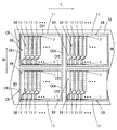
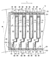
本実施の形態に係る集合体シート100は、複数のサスペンション基板1と枠部材CFとを備え、複数のサスペンション基板1は、整列状態で連結部JPにより支持される。枠部材CFの表面には、複数のサスペンション基板1に対応する複数の識別マークM1〜M4が設けられる。これにより、集合体シート100の複数のサスペンション基板1をAOIする際に、各サスペンション基板1の位置を識別することができる。
図9は、図8の集合体シート100上に形成される導体パターン25の開口部H1,H2およびその周辺を示す拡大平面図である。
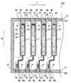
以下、他の実施の形態に係る集合体シート100について、上記実施の形態と異なる点を説明する。図10は、他の実施の形態に係る集合体シート100を示す一部拡大平面図である。
以下、請求項の各構成要素と実施の形態の各部との対応の例について説明するが、本発明は下記の例に限定されない。
10 支持基板
11 絶縁層
12 クロム膜
16 導体層
18 被覆層
20 サスペンション本体部
22,27 電極パッド
24 タング部
25 導体パターン
26 開口部
28 孔部
50 AOI装置
51 基板吸着台
52 CCDカメラ
53 光源
54 画像処理装置
55 メモリ
100 集合体シート
CF 枠部材
CR 枠領域
CR1〜CR4 枠部
H1〜H4 開口部
J 連結領域
JP 連結部
M1〜M4 識別マーク
RR 除去領域
SR 基板領域
Claims (10)
- 複数の回路付きサスペンション基板と、
前記複数の回路付きサスペンション基板を整列状態で一体的に支持する支持枠とを備え、
前記複数の回路付きサスペンション基板の各々は、一端部および他端部を有し、
前記支持枠は、前記複数の回路付きサスペンション基板の一端部が連結される第1の枠部と、前記複数の回路付きサスペンション基板の他端部が連結される第2の枠部とを有し、
前記第1の枠部の表面には、自動光学検査の際に前記複数の回路付きサスペンション基板の一端部の位置をそれぞれ識別するための複数の識別マークが前記複数の回路付きサスペンション基板の一端部に対応して設けられるとともに、前記第2の枠部の表面には、自動光学検査の際に前記複数の回路付きサスペンション基板の他端部の位置をそれぞれ識別するための複数の識別マークが前記複数の回路付きサスペンション基板の他端部に対応して設けられ、
前記複数の回路付きサスペンション基板および前記支持枠は、一体的に形成される複数の絶縁層と、前記複数の絶縁層上にそれぞれ形成される複数の導体パターンとを含み、
前記複数の識別マークは、前記支持枠の導体パターンに複数の開口部が形成されることにより露出する絶縁層の部分であることを特徴とする回路付きサスペンション基板集合体シート。 - 前記第1の枠部の前記複数の識別マークは、前記複数の回路付きサスペンション基板の一端部にそれぞれ対応して設けられる複数組の第1および第2の識別マークを含み、前記第2の枠部の前記複数の識別マークは、前記複数の回路付きサスペンション基板の他端部にそれぞれ対応して設けられる複数組の第3および第4の識別マークを含むことを特徴とする請求項1記載の回路付きサスペンション基板集合体シート。
- 各回路付きサスペンション基板に対応する第1、第2、第3および第4の識別マークは、当該回路付きサスペンション基板を取り囲むように配置されることを特徴とする請求項2記載の回路付きサスペンション基板集合体シート。
- 各回路付きサスペンション基板に対応する第1、第2、第3および第4の識別マークは、当該回路付きサスペンション基板の少なくとも一部を含む四角形状領域の四隅に配置されることを特徴とする請求項2または3記載の回路付きサスペンション基板集合体シート。
- 前記第1の枠部の前記複数の識別マークは、前記複数の回路付きサスペンション基板の一端部にそれぞれ対応して設けられる複数の第1の識別マークを含み、前記第2の枠部の前記複数の識別マークは、前記複数の回路付きサスペンション基板の他端部にそれぞれ対応して設けられる複数の第2の識別マークを含むことを特徴とする請求項1記載の回路付きサスペンション基板集合体シート。
- 前記複数の開口部は、連続的に湾曲する外周を有することを特徴とする請求項1〜5のいずれかに記載の回路付きサスペンション基板集合体シート。
- 前記複数の開口部は、略円形形状を有することを特徴とする請求項1〜6のいずれかに記載の回路付きサスペンション基板集合体シート。
- 前記複数の開口部の直径は、0.10mm以上0.15mm以下であることを特徴とする請求項1〜7のいずれかに記載の回路付きサスペンション基板集合体シート。
- 前記支持枠の前記導体パターンに形成される前記複数の開口部の各々の内面と前記支持枠の前記導体パターンの側面との間の最短の距離が0.05mm以上であることを特徴とする請求項1〜8のいずれかに記載の回路付きサスペンション基板集合体シート。
- 複数の回路付きサスペンション基板と前記複数の回路付きサスペンション基板を整列状態で一体的に支持する支持枠とを含む回路付きサスペンション基板集合体シートの製造方法であって、
金属基板を用意する工程と、
前記金属基板上に前記複数の回路付きサスペンション基板用の絶縁層および前記支持枠用の絶縁層をそれぞれ形成する工程と、
前記複数の回路付きサスペンション基板用の絶縁層上および前記支持枠用の絶縁層上に前記複数の回路付きサスペンション基板用の導体パターンおよび前記支持枠用の導体パターンをそれぞれ形成することにより複数の回路付きサスペンション基板および前記支持枠を作製するとともに、前記支持枠用の導体パターンに、前記複数の回路付きサスペンション基板の位置をそれぞれ識別するための複数の識別マークを前記複数の回路付きサスペンション基板に対応して設ける工程と、
前記複数の識別マークにより各回路付きサスペンション基板の位置を識別するとともに、各回路付きサスペンション基板の自動光学検査を行う工程と、
前記複数の回路付きサスペンション基板と前記支持枠との間の不要な金属基板および絶縁層の部分を除去する工程とを備え、
前記支持枠は、前記複数の回路付きサスペンション基板の一端部が連結される第1の枠部と、前記複数の回路付きサスペンション基板の他端部が連結される第2の枠部とを有し、
前記支持枠用の絶縁層は、前記第1の枠部用の第1の絶縁層と、前記第2の枠部用の第2の絶縁層とを含み、
前記支持枠用の導体パターンは、前記複数の回路付きサスペンション基板の一端部に対応する複数の開口部を有する第1の導体パターンと、前記複数の回路付きサスペンション基板の他端部に対応する複数の開口部を有する第2の導体パターンとを含み、
前記第1の導体パターンの前記複数の開口部から露出する前記第1の絶縁層の部分が前記複数の回路付きサスペンション基板の一端部の位置をそれぞれ識別するための前記複数の識別マークとなり、
前記第2の導体パターンの前記複数の開口部から露出する前記第2の絶縁層の部分が前記複数の回路付きサスペンション基板の他端部の位置をそれぞれ識別するための前記複数の識別マークとなることを特徴とする回路付きサスペンション基板集合体シートの製造方法。
Priority Applications (4)
| Application Number | Priority Date | Filing Date | Title |
|---|---|---|---|
| JP2009207662A JP4939583B2 (ja) | 2009-09-09 | 2009-09-09 | 回路付きサスペンション基板集合体シートおよびその製造方法 |
| CN201010256074.3A CN102024458B (zh) | 2009-09-09 | 2010-08-13 | 带电路的悬挂基板集合体片及其制造方法 |
| US12/874,846 US8477507B2 (en) | 2009-09-09 | 2010-09-02 | Suspension board assembly sheet with circuits and method for manufacturing the same |
| US13/888,889 US8897024B2 (en) | 2009-09-09 | 2013-05-07 | Method for manufacturing a suspension board assembly sheet with circuits |
Applications Claiming Priority (1)
| Application Number | Priority Date | Filing Date | Title |
|---|---|---|---|
| JP2009207662A JP4939583B2 (ja) | 2009-09-09 | 2009-09-09 | 回路付きサスペンション基板集合体シートおよびその製造方法 |
Publications (3)
| Publication Number | Publication Date |
|---|---|
| JP2011060925A JP2011060925A (ja) | 2011-03-24 |
| JP2011060925A5 JP2011060925A5 (ja) | 2011-05-06 |
| JP4939583B2 true JP4939583B2 (ja) | 2012-05-30 |
Family
ID=43647630
Family Applications (1)
| Application Number | Title | Priority Date | Filing Date |
|---|---|---|---|
| JP2009207662A Active JP4939583B2 (ja) | 2009-09-09 | 2009-09-09 | 回路付きサスペンション基板集合体シートおよびその製造方法 |
Country Status (3)
| Country | Link |
|---|---|
| US (2) | US8477507B2 (ja) |
| JP (1) | JP4939583B2 (ja) |
| CN (1) | CN102024458B (ja) |
Families Citing this family (15)
| Publication number | Priority date | Publication date | Assignee | Title |
|---|---|---|---|---|
| JP4939583B2 (ja) | 2009-09-09 | 2012-05-30 | 日東電工株式会社 | 回路付きサスペンション基板集合体シートおよびその製造方法 |
| JP2012221539A (ja) * | 2011-04-13 | 2012-11-12 | Dainippon Printing Co Ltd | サスペンション用基板、サスペンション、素子付サスペンション、ハードディスクドライブおよびサスペンション用基板の製造方法 |
| JP6016047B2 (ja) * | 2011-06-15 | 2016-10-26 | 大日本印刷株式会社 | サスペンション用基板、サスペンション、ヘッド付サスペンションおよびハードディスクドライブ |
| JP5273271B1 (ja) * | 2012-03-12 | 2013-08-28 | 大日本印刷株式会社 | 支持枠付サスペンション用基板 |
| JP6000073B2 (ja) * | 2012-11-08 | 2016-09-28 | 日東電工株式会社 | 回路付きサスペンション基板集合体シートおよびその製造方法 |
| JP6128439B2 (ja) * | 2013-10-04 | 2017-05-17 | 大日本印刷株式会社 | 多面付サスペンション用基板、サスペンション用基板、サスペンション、ヘッド付サスペンションおよびハードディスクドライブ |
| JP6180920B2 (ja) * | 2013-12-19 | 2017-08-16 | 日東電工株式会社 | 回路付きサスペンション基板集合体シートおよびその製造方法 |
| JP6315773B2 (ja) * | 2014-01-30 | 2018-04-25 | 日東電工株式会社 | 回路付サスペンション基板集合体シート |
| JP6329873B2 (ja) * | 2014-10-15 | 2018-05-23 | 日本発條株式会社 | ディスク装置用サスペンションのためのフレキシャ連鎖シート |
| JP6075436B2 (ja) * | 2015-11-17 | 2017-02-08 | 大日本印刷株式会社 | サスペンション用基板、サスペンション、素子付サスペンション、ハードディスクドライブおよび支持枠付サスペンション用基板 |
| JP6802688B2 (ja) * | 2016-11-02 | 2020-12-16 | 日東電工株式会社 | 配線回路基板 |
| JP7022562B2 (ja) * | 2017-10-25 | 2022-02-18 | 日東電工株式会社 | 回路付サスペンション基板集合体シートの製造方法 |
| JP7223504B2 (ja) * | 2018-03-02 | 2023-02-16 | 日東電工株式会社 | 回路付サスペンション基板集合体および回路付サスペンション基板集合体の製造方法 |
| JP7314077B2 (ja) * | 2020-02-10 | 2023-07-25 | 日本発條株式会社 | ディスク装置用サスペンションの製造方法と、その製造方法に使用されるサスペンションアセンブリ |
| JP7154344B1 (ja) * | 2021-05-13 | 2022-10-17 | 日東電工株式会社 | 配線回路基板および配線回路基板集合体シート |
Family Cites Families (44)
| Publication number | Priority date | Publication date | Assignee | Title |
|---|---|---|---|---|
| US4286201A (en) * | 1979-02-21 | 1981-08-25 | Amistar Corporation | Automatic part positioning system |
| JPS60263807A (ja) * | 1984-06-12 | 1985-12-27 | Dainippon Screen Mfg Co Ltd | プリント配線板のパタ−ン欠陥検査装置 |
| JP2645516B2 (ja) * | 1988-07-28 | 1997-08-25 | イビデン株式会社 | アイマークを備えたプリント配線板及びその製造方法 |
| JP2662477B2 (ja) * | 1992-06-03 | 1997-10-15 | 住友電気工業株式会社 | フレキシブルプリント配線板及びその製造方法 |
| US5894648A (en) * | 1996-02-26 | 1999-04-20 | Cencorp | High speed depaneling apparatus and method |
| KR100192760B1 (ko) * | 1996-02-29 | 1999-06-15 | 황인길 | 메탈 캐리어 프레임을 이용한 bag반도체 패키지의 제조방법 및 그반도체 패키지 |
| JP3776522B2 (ja) * | 1996-09-17 | 2006-05-17 | セイコープレシジョン株式会社 | 測距用受光装置及びその製造方法 |
| EP1028456A4 (en) * | 1997-09-19 | 2003-03-05 | Nikon Corp | PLATINUM, SCANNING ALIGNMENT DEVICE, AND SCANNING EXPOSURE METHOD, AND DEVICE MANUFACTURED THEREBY |
| TW448487B (en) * | 1997-11-22 | 2001-08-01 | Nippon Kogaku Kk | Exposure apparatus, exposure method and manufacturing method of device |
| US5945238A (en) * | 1998-02-06 | 1999-08-31 | Clear Logic, Inc. | Method of making a reusable photolithography mask |
| JP3579247B2 (ja) | 1998-05-13 | 2004-10-20 | 日本アビオニクス株式会社 | パターンの位置合わせ方法 |
| US6873800B1 (en) * | 1999-05-26 | 2005-03-29 | Jds Uniphase Corporation | Hot pluggable optical transceiver in a small form pluggable package |
| JP4017303B2 (ja) * | 1999-09-30 | 2007-12-05 | 日東電工株式会社 | 磁気ヘッドサスペンションの製造方法および磁気ヘッドサスペンション用の金属基板の検査方法 |
| US6576496B1 (en) * | 2000-08-21 | 2003-06-10 | Micron Technology, Inc. | Method and apparatus for encapsulating a multi-chip substrate array |
| AU2001279947A1 (en) * | 2000-08-23 | 2002-03-04 | Nicholas Michael Kavanagh | Transport linking frames |
| WO2002054460A1 (fr) * | 2000-12-27 | 2002-07-11 | Nikon Corporation | Dispositif d'exposition |
| JP3768819B2 (ja) * | 2001-01-31 | 2006-04-19 | 株式会社ルネサステクノロジ | 半導体装置の製造方法 |
| US6677918B2 (en) * | 2001-09-21 | 2004-01-13 | Yuji Yuhara | Light emitting diode display system |
| JP2003218475A (ja) * | 2002-01-22 | 2003-07-31 | Fuji Photo Film Co Ltd | 集合基板 |
| JP4095827B2 (ja) * | 2002-05-10 | 2008-06-04 | 株式会社ルネサステクノロジ | 半導体装置 |
| JP3758622B2 (ja) * | 2002-08-08 | 2006-03-22 | セイコーエプソン株式会社 | 光学装置、光学ユニット、および、プロジェクタ |
| US7321470B2 (en) * | 2002-10-08 | 2008-01-22 | Olympus Corporation | Camera |
| US6892449B1 (en) * | 2002-10-09 | 2005-05-17 | Cypress Semiconductor Corp. | Method of manufacturing electro-optical devices |
| US7129722B1 (en) * | 2002-10-09 | 2006-10-31 | Cypress Semiconductor Corp. | Methods of improving reliability of an electro-optical module |
| US6815729B1 (en) * | 2002-10-09 | 2004-11-09 | Cypress Semiconductor Corp. | Electro-optical apparatus |
| JP2004200607A (ja) * | 2002-12-20 | 2004-07-15 | Fuji Photo Film Co Ltd | 集合プリント配線板 |
| TWI239684B (en) * | 2003-04-16 | 2005-09-11 | Jsr Corp | Anisotropic conductive connector and electric inspection device for circuit device |
| US7281860B2 (en) * | 2003-06-06 | 2007-10-16 | Sharp Kabushiki Kaisha | Optical transmitter |
| US20060076104A1 (en) * | 2004-09-27 | 2006-04-13 | Ngk Spark Plug Co., Ltd. | Film peeling apparatus and method of manufacturing wiring board |
| US7352969B2 (en) * | 2004-09-30 | 2008-04-01 | Intel Corporation | Fiber optic communication assembly |
| JP4515276B2 (ja) * | 2005-01-31 | 2010-07-28 | 日東電工株式会社 | 配線回路基板集合体 |
| US7883278B2 (en) * | 2005-07-04 | 2011-02-08 | Fuji Xerox Co., Ltd. | Optical module and optical transmission device |
| JP4762734B2 (ja) * | 2006-01-25 | 2011-08-31 | 日東電工株式会社 | 配線回路基板集合体シートおよびその製造方法 |
| JP4757083B2 (ja) * | 2006-04-13 | 2011-08-24 | 日東電工株式会社 | 配線回路基板集合体シート |
| KR20080081605A (ko) * | 2007-03-06 | 2008-09-10 | 삼성전자주식회사 | 절연 모기판에 얼라인 마크를 형성하는 단계를 포함하는액정 표시 장치의 제조 방법 |
| WO2008146350A1 (ja) * | 2007-05-25 | 2008-12-04 | Ibiden Co., Ltd. | ハニカム構造体及びハニカム構造体の製造方法 |
| JP5147591B2 (ja) * | 2008-08-06 | 2013-02-20 | 日東電工株式会社 | 回路付サスペンション基板、その製造方法および回路付サスペンション基板の位置決め方法 |
| US8760187B2 (en) * | 2008-12-03 | 2014-06-24 | L-3 Communications Corp. | Thermocentric alignment of elements on parts of an apparatus |
| JP5285441B2 (ja) * | 2009-01-09 | 2013-09-11 | 日東電工株式会社 | 配線回路基板集合体シート |
| JP5204679B2 (ja) * | 2009-01-23 | 2013-06-05 | 日東電工株式会社 | 回路付サスペンション基板 |
| IT1392992B1 (it) * | 2009-02-23 | 2012-04-02 | Applied Materials Inc | Procedimento e apparecchiatura per la stampa serigrafica di uno schema a strato multiplo |
| JP4939583B2 (ja) | 2009-09-09 | 2012-05-30 | 日東電工株式会社 | 回路付きサスペンション基板集合体シートおよびその製造方法 |
| JP5538049B2 (ja) * | 2010-04-22 | 2014-07-02 | 日東電工株式会社 | フォトマスクと基材との位置合わせ方法および配線回路基板の製造方法 |
| JP5502647B2 (ja) * | 2010-08-06 | 2014-05-28 | 日東電工株式会社 | 配線回路基板集合体シートおよびその製造方法 |
-
2009
- 2009-09-09 JP JP2009207662A patent/JP4939583B2/ja active Active
-
2010
- 2010-08-13 CN CN201010256074.3A patent/CN102024458B/zh active Active
- 2010-09-02 US US12/874,846 patent/US8477507B2/en active Active
-
2013
- 2013-05-07 US US13/888,889 patent/US8897024B2/en not_active Expired - Fee Related
Also Published As
| Publication number | Publication date |
|---|---|
| CN102024458A (zh) | 2011-04-20 |
| US8477507B2 (en) | 2013-07-02 |
| US8897024B2 (en) | 2014-11-25 |
| US20130247371A1 (en) | 2013-09-26 |
| US20110058347A1 (en) | 2011-03-10 |
| CN102024458B (zh) | 2014-08-27 |
| JP2011060925A (ja) | 2011-03-24 |
Similar Documents
| Publication | Publication Date | Title |
|---|---|---|
| JP4939583B2 (ja) | 回路付きサスペンション基板集合体シートおよびその製造方法 | |
| JP4640815B2 (ja) | 配線回路基板集合体シートおよびその製造方法 | |
| US7561434B2 (en) | Wired circuit board and method for manufacturing wired circuit board and mounting electronic component thereon | |
| JP4762734B2 (ja) | 配線回路基板集合体シートおよびその製造方法 | |
| US7358619B2 (en) | Tape carrier for TAB | |
| US9251818B2 (en) | Suspension board with circuits for accurate posture angle adjustment, and method for manufacturing the same | |
| JP5538048B2 (ja) | アライメントマークの検出方法および配線回路基板の製造方法 | |
| JP2012059756A (ja) | 配線回路基板およびその製造方法 | |
| JP5005307B2 (ja) | 配線回路基板およびその製造方法 | |
| JP5528273B2 (ja) | 配線回路基板、配線回路基板集合体シートおよびその製造方法 | |
| US8222530B2 (en) | Wired circuit board assembly sheet | |
| JP2007287799A (ja) | 配線回路基板集合体シート | |
| JP2007115828A (ja) | 回路付サスペンション基板集合体シートおよびその製造方法 | |
| US8866020B2 (en) | Method for manufacturing printed circuit board, method for manufacturing printed circuit board assembly sheet, printed circuit board, and printed circuit board assembly sheet | |
| KR101572089B1 (ko) | 인쇄회로기판 검사방법 | |
| JP2011171373A (ja) | 配線回路基板の検査方法および製造方法 | |
| KR20100088874A (ko) | 인쇄회로기판의 노광방법 및 이를 포함하는 인쇄회로기판의제조방법 | |
| JP4792660B2 (ja) | 回路基板の製造方法 | |
| JP4358682B2 (ja) | 回路付サスペンション基板の導体パターンの導通検査方法 | |
| JP2010192610A (ja) | 多面付け現像パターン形成済プリント配線板用基材の製造方法および検査方法、多面付けプリント配線板の製造方法および検査方法、半導体装置の製造方法、ならびに露光マスク | |
| JP3660187B2 (ja) | 磁気ヘッドサスペンションの製造方法および磁気ヘッドサスペンション用の金属基板の検査方法ならびにマスクの形成方法 | |
| TWI386129B (zh) | 電路板文字漏印之檢測方法 | |
| JP7252767B2 (ja) | 回路付サスペンション基板の製造方法、および、回路付サスペンション基板集合体 | |
| JP5671597B2 (ja) | 配線回路基板集合体シートの製造方法 | |
| CN113777113A (zh) | 一种灯板的光学检测方法及灯板制作方法 |
Legal Events
| Date | Code | Title | Description |
|---|---|---|---|
| A977 | Report on retrieval |
Free format text: JAPANESE INTERMEDIATE CODE: A971007 Effective date: 20110628 |
|
| A131 | Notification of reasons for refusal |
Free format text: JAPANESE INTERMEDIATE CODE: A131 Effective date: 20110906 |
|
| A521 | Request for written amendment filed |
Free format text: JAPANESE INTERMEDIATE CODE: A523 Effective date: 20111101 |
|
| TRDD | Decision of grant or rejection written | ||
| A01 | Written decision to grant a patent or to grant a registration (utility model) |
Free format text: JAPANESE INTERMEDIATE CODE: A01 Effective date: 20120131 |
|
| A01 | Written decision to grant a patent or to grant a registration (utility model) |
Free format text: JAPANESE INTERMEDIATE CODE: A01 |
|
| A61 | First payment of annual fees (during grant procedure) |
Free format text: JAPANESE INTERMEDIATE CODE: A61 Effective date: 20120224 |
|
| FPAY | Renewal fee payment (event date is renewal date of database) |
Free format text: PAYMENT UNTIL: 20150302 Year of fee payment: 3 |
|
| R150 | Certificate of patent or registration of utility model |
Free format text: JAPANESE INTERMEDIATE CODE: R150 Ref document number: 4939583 Country of ref document: JP Free format text: JAPANESE INTERMEDIATE CODE: R150 |
|
| R250 | Receipt of annual fees |
Free format text: JAPANESE INTERMEDIATE CODE: R250 |
|
| R250 | Receipt of annual fees |
Free format text: JAPANESE INTERMEDIATE CODE: R250 |
|
| R250 | Receipt of annual fees |
Free format text: JAPANESE INTERMEDIATE CODE: R250 |
|
| R250 | Receipt of annual fees |
Free format text: JAPANESE INTERMEDIATE CODE: R250 |
|
| R250 | Receipt of annual fees |
Free format text: JAPANESE INTERMEDIATE CODE: R250 |
|
| R250 | Receipt of annual fees |
Free format text: JAPANESE INTERMEDIATE CODE: R250 |
|
| R250 | Receipt of annual fees |
Free format text: JAPANESE INTERMEDIATE CODE: R250 |
|
| R250 | Receipt of annual fees |
Free format text: JAPANESE INTERMEDIATE CODE: R250 |
|
| R250 | Receipt of annual fees |
Free format text: JAPANESE INTERMEDIATE CODE: R250 |
|
| R250 | Receipt of annual fees |
Free format text: JAPANESE INTERMEDIATE CODE: R250 |