JP4370789B2 - プラズマ処理装置及び可変インピーダンス手段の校正方法 - Google Patents
プラズマ処理装置及び可変インピーダンス手段の校正方法 Download PDFInfo
- Publication number
- JP4370789B2 JP4370789B2 JP2003060670A JP2003060670A JP4370789B2 JP 4370789 B2 JP4370789 B2 JP 4370789B2 JP 2003060670 A JP2003060670 A JP 2003060670A JP 2003060670 A JP2003060670 A JP 2003060670A JP 4370789 B2 JP4370789 B2 JP 4370789B2
- Authority
- JP
- Japan
- Prior art keywords
- impedance
- plasma processing
- variable
- processing apparatus
- electrode
- Prior art date
- Legal status (The legal status is an assumption and is not a legal conclusion. Google has not performed a legal analysis and makes no representation as to the accuracy of the status listed.)
- Expired - Fee Related
Links
- 238000012545 processing Methods 0.000 title claims description 177
- 238000000034 method Methods 0.000 title claims description 118
- 230000008569 process Effects 0.000 claims description 87
- 238000005530 etching Methods 0.000 claims description 44
- 238000009832 plasma treatment Methods 0.000 claims description 8
- 238000001514 detection method Methods 0.000 claims description 4
- 239000003990 capacitor Substances 0.000 description 66
- 238000010586 diagram Methods 0.000 description 33
- 230000008859 change Effects 0.000 description 21
- 239000007789 gas Substances 0.000 description 17
- 238000011156 evaluation Methods 0.000 description 8
- VYPSYNLAJGMNEJ-UHFFFAOYSA-N silicon dioxide Inorganic materials O=[Si]=O VYPSYNLAJGMNEJ-UHFFFAOYSA-N 0.000 description 8
- 239000004065 semiconductor Substances 0.000 description 7
- 238000005259 measurement Methods 0.000 description 6
- 230000000694 effects Effects 0.000 description 5
- 238000005516 engineering process Methods 0.000 description 5
- 230000007246 mechanism Effects 0.000 description 4
- XAGFODPZIPBFFR-UHFFFAOYSA-N aluminium Chemical compound [Al] XAGFODPZIPBFFR-UHFFFAOYSA-N 0.000 description 3
- 229910052782 aluminium Inorganic materials 0.000 description 3
- 238000004380 ashing Methods 0.000 description 3
- 230000003028 elevating effect Effects 0.000 description 3
- 230000004048 modification Effects 0.000 description 3
- 238000012986 modification Methods 0.000 description 3
- 229920002120 photoresistant polymer Polymers 0.000 description 3
- 239000000377 silicon dioxide Substances 0.000 description 3
- BOTDANWDWHJENH-UHFFFAOYSA-N Tetraethyl orthosilicate Chemical compound CCO[Si](OCC)(OCC)OCC BOTDANWDWHJENH-UHFFFAOYSA-N 0.000 description 2
- 229910052681 coesite Inorganic materials 0.000 description 2
- 229910052906 cristobalite Inorganic materials 0.000 description 2
- 230000007423 decrease Effects 0.000 description 2
- 238000009434 installation Methods 0.000 description 2
- 238000004519 manufacturing process Methods 0.000 description 2
- 229910021420 polycrystalline silicon Inorganic materials 0.000 description 2
- 229920005591 polysilicon Polymers 0.000 description 2
- 239000000523 sample Substances 0.000 description 2
- 235000012239 silicon dioxide Nutrition 0.000 description 2
- LIVNPJMFVYWSIS-UHFFFAOYSA-N silicon monoxide Chemical compound [Si-]#[O+] LIVNPJMFVYWSIS-UHFFFAOYSA-N 0.000 description 2
- 239000007787 solid Substances 0.000 description 2
- 229910052682 stishovite Inorganic materials 0.000 description 2
- 239000000758 substrate Substances 0.000 description 2
- 229910052905 tridymite Inorganic materials 0.000 description 2
- XUIMIQQOPSSXEZ-UHFFFAOYSA-N Silicon Chemical compound [Si] XUIMIQQOPSSXEZ-UHFFFAOYSA-N 0.000 description 1
- 238000000137 annealing Methods 0.000 description 1
- 230000008901 benefit Effects 0.000 description 1
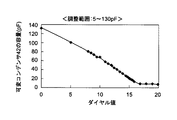
- 238000011088 calibration curve Methods 0.000 description 1
- 239000000919 ceramic Substances 0.000 description 1
- 230000003247 decreasing effect Effects 0.000 description 1
- 238000009792 diffusion process Methods 0.000 description 1
- 239000011521 glass Substances 0.000 description 1
- 239000011368 organic material Substances 0.000 description 1
- 230000001590 oxidative effect Effects 0.000 description 1
- 230000002093 peripheral effect Effects 0.000 description 1
- 238000004886 process control Methods 0.000 description 1
- 239000010453 quartz Substances 0.000 description 1
- 229910052710 silicon Inorganic materials 0.000 description 1
- 239000010703 silicon Substances 0.000 description 1
- 229910052814 silicon oxide Inorganic materials 0.000 description 1
Images


Classifications
-
- H—ELECTRICITY
- H01—ELECTRIC ELEMENTS
- H01J—ELECTRIC DISCHARGE TUBES OR DISCHARGE LAMPS
- H01J37/00—Discharge tubes with provision for introducing objects or material to be exposed to the discharge, e.g. for the purpose of examination or processing thereof
- H01J37/32—Gas-filled discharge tubes
- H01J37/32009—Arrangements for generation of plasma specially adapted for examination or treatment of objects, e.g. plasma sources
- H01J37/32082—Radio frequency generated discharge
- H01J37/32174—Circuits specially adapted for controlling the RF discharge
-
- H—ELECTRICITY
- H01—ELECTRIC ELEMENTS
- H01J—ELECTRIC DISCHARGE TUBES OR DISCHARGE LAMPS
- H01J37/00—Discharge tubes with provision for introducing objects or material to be exposed to the discharge, e.g. for the purpose of examination or processing thereof
- H01J37/32—Gas-filled discharge tubes
- H01J37/32009—Arrangements for generation of plasma specially adapted for examination or treatment of objects, e.g. plasma sources
- H01J37/32082—Radio frequency generated discharge
- H01J37/321—Radio frequency generated discharge the radio frequency energy being inductively coupled to the plasma
Landscapes
- Physics & Mathematics (AREA)
- Engineering & Computer Science (AREA)
- Plasma & Fusion (AREA)
- Chemical & Material Sciences (AREA)
- Analytical Chemistry (AREA)
- Plasma Technology (AREA)
- Drying Of Semiconductors (AREA)
- Physical Or Chemical Processes And Apparatus (AREA)
- Chemical Vapour Deposition (AREA)
Priority Applications (7)
| Application Number | Priority Date | Filing Date | Title |
|---|---|---|---|
| JP2003060670A JP4370789B2 (ja) | 2002-07-12 | 2003-03-06 | プラズマ処理装置及び可変インピーダンス手段の校正方法 |
| US10/615,915 US7527016B2 (en) | 2002-07-12 | 2003-07-10 | Plasma processing apparatus |
| CNB031466818A CN100355038C (zh) | 2002-07-12 | 2003-07-11 | 等离子体处理装置和可变阻抗装置的校正方法 |
| CN2007101823491A CN101160014B (zh) | 2002-07-12 | 2003-07-11 | 等离子体处理装置和可变阻抗装置的校正方法 |
| TW092119056A TW200402759A (en) | 2002-07-12 | 2003-07-11 | Plasma treatment apparatus |
| KR1020030047603A KR101054558B1 (ko) | 2002-07-12 | 2003-07-12 | 플라즈마 처리 장치 및 가변 임피던스 수단의 교정 방법 |
| US11/756,097 US8251011B2 (en) | 2002-07-12 | 2007-05-31 | Plasma processing apparatus |
Applications Claiming Priority (2)
| Application Number | Priority Date | Filing Date | Title |
|---|---|---|---|
| JP2002204928 | 2002-07-12 | ||
| JP2003060670A JP4370789B2 (ja) | 2002-07-12 | 2003-03-06 | プラズマ処理装置及び可変インピーダンス手段の校正方法 |
Related Child Applications (1)
| Application Number | Title | Priority Date | Filing Date |
|---|---|---|---|
| JP2008331537A Division JP4985637B2 (ja) | 2002-07-12 | 2008-12-25 | プラズマ処理方法 |
Publications (3)
| Publication Number | Publication Date |
|---|---|
| JP2004096066A JP2004096066A (ja) | 2004-03-25 |
| JP2004096066A5 JP2004096066A5 (enExample) | 2006-03-23 |
| JP4370789B2 true JP4370789B2 (ja) | 2009-11-25 |
Family
ID=31497586
Family Applications (1)
| Application Number | Title | Priority Date | Filing Date |
|---|---|---|---|
| JP2003060670A Expired - Fee Related JP4370789B2 (ja) | 2002-07-12 | 2003-03-06 | プラズマ処理装置及び可変インピーダンス手段の校正方法 |
Country Status (4)
| Country | Link |
|---|---|
| US (2) | US7527016B2 (enExample) |
| JP (1) | JP4370789B2 (enExample) |
| CN (1) | CN100355038C (enExample) |
| TW (1) | TW200402759A (enExample) |
Families Citing this family (80)
| Publication number | Priority date | Publication date | Assignee | Title |
|---|---|---|---|---|
| US20070048882A1 (en) * | 2000-03-17 | 2007-03-01 | Applied Materials, Inc. | Method to reduce plasma-induced charging damage |
| US8048806B2 (en) * | 2000-03-17 | 2011-11-01 | Applied Materials, Inc. | Methods to avoid unstable plasma states during a process transition |
| US20110104381A1 (en) * | 2004-01-15 | 2011-05-05 | Stefan Laure | Plasma Treatment of Large-Scale Components |
| JP4558365B2 (ja) * | 2004-03-26 | 2010-10-06 | 株式会社神戸製鋼所 | プラズマ処理装置及びプラズマ処理方法 |
| US7435926B2 (en) * | 2004-03-31 | 2008-10-14 | Lam Research Corporation | Methods and array for creating a mathematical model of a plasma processing system |
| JP4606944B2 (ja) * | 2004-06-02 | 2011-01-05 | 東京エレクトロン株式会社 | プラズマ処理装置およびインピーダンス調整方法 |
| KR100710923B1 (ko) | 2004-06-02 | 2007-04-23 | 동경 엘렉트론 주식회사 | 플라즈마 처리장치 및 임피던스 조정방법 |
| US20060021580A1 (en) * | 2004-06-02 | 2006-02-02 | Tokyo Electron Limited | Plasma processing apparatus and impedance adjustment method |
| CN1734712A (zh) * | 2004-07-30 | 2006-02-15 | 东京毅力科创株式会社 | 等离子体处理装置以及等离子体处理方法 |
| US20060037704A1 (en) * | 2004-07-30 | 2006-02-23 | Tokyo Electron Limited | Plasma Processing apparatus and method |
| JP4676189B2 (ja) * | 2004-11-02 | 2011-04-27 | 東京エレクトロン株式会社 | 高周波給電装置及びプラズマ処理装置 |
| JP5086092B2 (ja) * | 2004-11-12 | 2012-11-28 | エリコン・ソーラー・アクチェンゲゼルシャフト,トリュープバッハ | 大面積基板に好適な容量結合型rfプラズマ反応器のインピーダンス整合 |
| JP4546303B2 (ja) * | 2005-03-24 | 2010-09-15 | 東京エレクトロン株式会社 | プラズマ処理装置 |
| US7993489B2 (en) * | 2005-03-31 | 2011-08-09 | Tokyo Electron Limited | Capacitive coupling plasma processing apparatus and method for using the same |
| WO2006108395A1 (de) * | 2005-04-11 | 2006-10-19 | Dr. Laure Plasmatechnologie Gmbh | Vorrichtung und verfahren zur plasmabeschichtung |
| US7780814B2 (en) * | 2005-07-08 | 2010-08-24 | Applied Materials, Inc. | Wafer pre-clean reactor cable termination for selective suppression/reflection of source and bias frequency cross products |
| CN100362619C (zh) * | 2005-08-05 | 2008-01-16 | 中微半导体设备(上海)有限公司 | 真空反应室的射频匹配耦合网络及其配置方法 |
| JP2007250967A (ja) * | 2006-03-17 | 2007-09-27 | Tokyo Electron Ltd | プラズマ処理装置および方法とフォーカスリング |
| US7758929B2 (en) * | 2006-03-31 | 2010-07-20 | Tokyo Electron Limited | Plasma processing apparatus and method |
| US7611603B2 (en) | 2006-03-31 | 2009-11-03 | Tokyo Electron Limited | Plasma processing apparatus having impedance varying electrodes |
| JP5192209B2 (ja) | 2006-10-06 | 2013-05-08 | 東京エレクトロン株式会社 | プラズマエッチング装置、プラズマエッチング方法およびコンピュータ読取可能な記憶媒体 |
| JP5491648B2 (ja) * | 2006-10-06 | 2014-05-14 | 東京エレクトロン株式会社 | プラズマエッチング装置およびプラズマエッチング方法 |
| JP2008186939A (ja) * | 2007-01-29 | 2008-08-14 | Tokyo Electron Ltd | プラズマ処理装置及びプラズマ処理方法並びに記憶媒体 |
| US8076247B2 (en) | 2007-01-30 | 2011-12-13 | Applied Materials, Inc. | Plasma process uniformity across a wafer by controlling RF phase between opposing electrodes |
| US7879731B2 (en) * | 2007-01-30 | 2011-02-01 | Applied Materials, Inc. | Improving plasma process uniformity across a wafer by apportioning power among plural VHF sources |
| US7968469B2 (en) * | 2007-01-30 | 2011-06-28 | Applied Materials, Inc. | Method of processing a workpiece in a plasma reactor with variable height ground return path to control plasma ion density uniformity |
| US20080178803A1 (en) * | 2007-01-30 | 2008-07-31 | Collins Kenneth S | Plasma reactor with ion distribution uniformity controller employing plural vhf sources |
| DE112008000490A5 (de) * | 2007-02-26 | 2009-11-26 | Dr. Laure Plasmatechnologie Gmbh | Vorrichtung und ein Verfahren zur plasmagestützten Beschichtung und Oberflächenbehandlung grossvolumiger Bauteile |
| JP4903610B2 (ja) * | 2007-03-27 | 2012-03-28 | 東京エレクトロン株式会社 | プラズマ処理装置 |
| JP5160802B2 (ja) * | 2007-03-27 | 2013-03-13 | 東京エレクトロン株式会社 | プラズマ処理装置 |
| JP5348848B2 (ja) * | 2007-03-28 | 2013-11-20 | 東京エレクトロン株式会社 | プラズマ処理装置 |
| JP2009081812A (ja) * | 2007-09-27 | 2009-04-16 | Nec Electronics Corp | 信号処理装置および信号処理方法 |
| JP5165993B2 (ja) * | 2007-10-18 | 2013-03-21 | 東京エレクトロン株式会社 | プラズマ処理装置 |
| JP2009187673A (ja) * | 2008-02-01 | 2009-08-20 | Nec Electronics Corp | プラズマ処理装置及び方法 |
| JP2009239012A (ja) | 2008-03-27 | 2009-10-15 | Tokyo Electron Ltd | プラズマ処理装置及びプラズマエッチング方法 |
| US8920611B2 (en) * | 2008-07-15 | 2014-12-30 | Applied Materials, Inc. | Method for controlling radial distribution of plasma ion density and ion energy at a workpiece surface by multi-frequency RF impedance tuning |
| US9017533B2 (en) * | 2008-07-15 | 2015-04-28 | Applied Materials, Inc. | Apparatus for controlling radial distribution of plasma ion density and ion energy at a workpiece surface by multi-frequency RF impedance tuning |
| CN100595886C (zh) * | 2008-09-26 | 2010-03-24 | 中国科学院微电子研究所 | 一种消除反应离子刻蚀自偏压的方法及系统 |
| AU2009327173B2 (en) * | 2008-12-17 | 2013-09-19 | Vestas Wind Systems A/S | Method and system for testing wind turbine plants |
| US9275838B2 (en) * | 2009-09-02 | 2016-03-01 | Lam Research Corporation | Arrangements for manipulating plasma confinement within a plasma processing system and methods thereof |
| JP5566389B2 (ja) * | 2009-09-25 | 2014-08-06 | 京セラ株式会社 | 堆積膜形成装置および堆積膜形成方法 |
| US20110209995A1 (en) * | 2010-03-01 | 2011-09-01 | Applied Materials, Inc. | Physical Vapor Deposition With A Variable Capacitive Tuner and Feedback Circuit |
| JP5498217B2 (ja) * | 2010-03-24 | 2014-05-21 | 株式会社ダイヘン | 高周波測定装置、および、高周波測定装置の校正方法 |
| JP5571996B2 (ja) * | 2010-03-31 | 2014-08-13 | 東京エレクトロン株式会社 | プラズマ処理方法及びプラズマ処理装置 |
| JP2012060104A (ja) * | 2010-08-11 | 2012-03-22 | Toshiba Corp | 電源制御装置、プラズマ処理装置、及びプラズマ処理方法 |
| US10586686B2 (en) | 2011-11-22 | 2020-03-10 | Law Research Corporation | Peripheral RF feed and symmetric RF return for symmetric RF delivery |
| US8932429B2 (en) * | 2012-02-23 | 2015-01-13 | Lam Research Corporation | Electronic knob for tuning radial etch non-uniformity at VHF frequencies |
| US9881772B2 (en) * | 2012-03-28 | 2018-01-30 | Lam Research Corporation | Multi-radiofrequency impedance control for plasma uniformity tuning |
| KR20140059422A (ko) * | 2012-11-08 | 2014-05-16 | 엘아이지에이디피 주식회사 | 유도 결합 플라즈마 처리 장치 및 그 제어방법 |
| US9401264B2 (en) * | 2013-10-01 | 2016-07-26 | Lam Research Corporation | Control of impedance of RF delivery path |
| JP2015053384A (ja) * | 2013-09-06 | 2015-03-19 | 東京エレクトロン株式会社 | プラズマ処理方法及びプラズマ処理装置 |
| JP6573325B2 (ja) * | 2013-12-17 | 2019-09-11 | 東京エレクトロン株式会社 | プラズマ密度を制御するシステムおよび方法 |
| JP2016046357A (ja) * | 2014-08-22 | 2016-04-04 | 株式会社日立ハイテクノロジーズ | プラズマ処理装置 |
| CN106604802B (zh) * | 2014-09-02 | 2019-05-31 | 株式会社荏原制作所 | 终点检测方法、研磨装置及研磨方法 |
| JP6584329B2 (ja) * | 2016-01-19 | 2019-10-02 | 東京エレクトロン株式会社 | プラズマ処理装置 |
| JPWO2018051447A1 (ja) * | 2016-09-15 | 2019-06-24 | 株式会社日立国際電気 | 整合器 |
| US10896806B2 (en) * | 2016-11-03 | 2021-01-19 | En2Core Technology, Inc. | Inductive coil structure and inductively coupled plasma generation system |
| US10903046B2 (en) * | 2016-11-03 | 2021-01-26 | En2Core Technology, Inc. | Inductive coil structure and inductively coupled plasma generation system |
| US10541114B2 (en) * | 2016-11-03 | 2020-01-21 | En2Core Technology, Inc. | Inductive coil structure and inductively coupled plasma generation system |
| US20180175819A1 (en) * | 2016-12-16 | 2018-06-21 | Lam Research Corporation | Systems and methods for providing shunt cancellation of parasitic components in a plasma reactor |
| CN107665829B (zh) | 2017-08-24 | 2019-12-17 | 长江存储科技有限责任公司 | 晶圆混合键合中提高金属引线制程安全性的方法 |
| US10269540B1 (en) * | 2018-01-25 | 2019-04-23 | Advanced Energy Industries, Inc. | Impedance matching system and method of operating the same |
| US10892142B2 (en) | 2018-03-16 | 2021-01-12 | Samsung Electronics Co., Ltd. | System for fabricating a semiconductor device |
| JP7049883B2 (ja) * | 2018-03-28 | 2022-04-07 | 東京エレクトロン株式会社 | ボロン系膜の成膜方法および成膜装置 |
| JP7085963B2 (ja) * | 2018-10-29 | 2022-06-17 | 東京エレクトロン株式会社 | プラズマ処理装置およびプラズマ処理方法 |
| CN112913140B (zh) | 2018-11-09 | 2024-09-03 | 应用材料公司 | 用于处理腔室的射频滤波器系统 |
| JP7154119B2 (ja) * | 2018-12-06 | 2022-10-17 | 東京エレクトロン株式会社 | 制御方法及びプラズマ処理装置 |
| US11437262B2 (en) * | 2018-12-12 | 2022-09-06 | Applied Materials, Inc | Wafer de-chucking detection and arcing prevention |
| WO2020257965A1 (en) * | 2019-06-24 | 2020-12-30 | Trumpf Huettinger (Shanghai) Co., Ltd. | Method of adjusting the output power of a power supply supplying electrical power to a plasma, plasma apparatus and power supply |
| KR102189323B1 (ko) * | 2019-07-16 | 2020-12-11 | 세메스 주식회사 | 기판 처리 장치 및 기판 처리 방법 |
| KR102295727B1 (ko) * | 2019-09-05 | 2021-08-31 | 한양대학교 산학협력단 | 기판 처리 장치 |
| KR102223875B1 (ko) * | 2019-10-30 | 2021-03-05 | 주식회사 뉴파워 프라즈마 | 다중 주파수를 사용하는 건식 식각 장비를 위한 고주파 전원 장치 |
| CN120856086A (zh) * | 2019-11-15 | 2025-10-28 | 朗姆研究公司 | 调谐电路中基于频率的阻抗调整 |
| JP7413099B2 (ja) * | 2020-03-16 | 2024-01-15 | 東京エレクトロン株式会社 | 成膜方法および成膜装置 |
| CN113820531B (zh) | 2020-06-19 | 2024-07-12 | 拓荆科技股份有限公司 | 一种射频系统状态受控的半导体设备 |
| TW202226897A (zh) * | 2020-11-06 | 2022-07-01 | 日商東京威力科創股份有限公司 | 濾波器電路 |
| US11961712B2 (en) | 2021-04-26 | 2024-04-16 | Advanced Energy Industries, Inc. | Combining the determination of single and mutual, preset preserving, impedance loads with advances in single and double sensor calibration techniques in the application of single and pairwise calibration of sensors |
| KR20230042824A (ko) | 2021-09-23 | 2023-03-30 | 삼성전자주식회사 | 플라즈마 제어 장치 및 플라즈마 처리 시스템 |
| KR102660299B1 (ko) * | 2021-12-29 | 2024-04-26 | 세메스 주식회사 | 기판 처리 장치, 고조파 제어 유닛 및 고조파 제어 방법 |
| US20240047938A1 (en) * | 2022-08-05 | 2024-02-08 | Satius Holding, Llc | Capacitive Coupling for Optical or Laser Diodes |
Family Cites Families (35)
| Publication number | Priority date | Publication date | Assignee | Title |
|---|---|---|---|---|
| US4340461A (en) * | 1980-09-10 | 1982-07-20 | International Business Machines Corp. | Modified RIE chamber for uniform silicon etching |
| JPS58158929A (ja) | 1982-03-17 | 1983-09-21 | Kokusai Electric Co Ltd | プラズマ発生装置 |
| JPH02298024A (ja) * | 1989-05-12 | 1990-12-10 | Tadahiro Omi | リアクティブイオンエッチング装置 |
| JPH0354825A (ja) | 1989-07-21 | 1991-03-08 | Tokyo Electron Ltd | プラズマ処理装置 |
| JPH06112167A (ja) * | 1992-09-29 | 1994-04-22 | Tokyo Electron Ltd | プラズマ装置 |
| JP3251087B2 (ja) | 1993-02-16 | 2002-01-28 | 東京エレクトロン株式会社 | プラズマ処理装置 |
| US5849372A (en) * | 1993-09-17 | 1998-12-15 | Isis Innovation Limited | RF plasma reactor and methods of generating RF plasma |
| US5815047A (en) * | 1993-10-29 | 1998-09-29 | Applied Materials, Inc. | Fast transition RF impedance matching network for plasma reactor ignition |
| JP3162245B2 (ja) | 1994-04-20 | 2001-04-25 | 東京エレクトロン株式会社 | プラズマ処理方法及びプラズマ処理装置 |
| US5474648A (en) * | 1994-07-29 | 1995-12-12 | Lsi Logic Corporation | Uniform and repeatable plasma processing |
| US6095084A (en) * | 1996-02-02 | 2000-08-01 | Applied Materials, Inc. | High density plasma process chamber |
| US6252354B1 (en) * | 1996-11-04 | 2001-06-26 | Applied Materials, Inc. | RF tuning method for an RF plasma reactor using frequency servoing and power, voltage, current or DI/DT control |
| US6174450B1 (en) * | 1997-04-16 | 2001-01-16 | Lam Research Corporation | Methods and apparatus for controlling ion energy and plasma density in a plasma processing system |
| JP3022806B2 (ja) | 1997-05-15 | 2000-03-21 | 九州日本電気株式会社 | 半導体装置の製造装置及びその調整方法 |
| JPH10125665A (ja) | 1997-11-04 | 1998-05-15 | Tadahiro Omi | プラズマプロセス用装置 |
| US7004107B1 (en) * | 1997-12-01 | 2006-02-28 | Applied Materials Inc. | Method and apparatus for monitoring and adjusting chamber impedance |
| JP3565311B2 (ja) * | 1997-12-17 | 2004-09-15 | アルプス電気株式会社 | プラズマ処理装置 |
| JP4130255B2 (ja) * | 1998-04-08 | 2008-08-06 | キヤノンアネルバ株式会社 | プラズマ処理装置 |
| US6259334B1 (en) * | 1998-12-22 | 2001-07-10 | Lam Research Corporation | Methods for controlling an RF matching network |
| JP4450883B2 (ja) | 1999-03-30 | 2010-04-14 | 東京エレクトロン株式会社 | プラズマ処理装置 |
| US6232236B1 (en) * | 1999-08-03 | 2001-05-15 | Applied Materials, Inc. | Apparatus and method for controlling plasma uniformity in a semiconductor wafer processing system |
| TW492041B (en) * | 2000-02-14 | 2002-06-21 | Tokyo Electron Ltd | Method and device for attenuating harmonics in semiconductor plasma processing systems |
| US6894245B2 (en) * | 2000-03-17 | 2005-05-17 | Applied Materials, Inc. | Merie plasma reactor with overhead RF electrode tuned to the plasma with arcing suppression |
| US7030335B2 (en) * | 2000-03-17 | 2006-04-18 | Applied Materials, Inc. | Plasma reactor with overhead RF electrode tuned to the plasma with arcing suppression |
| TW483037B (en) * | 2000-03-24 | 2002-04-11 | Hitachi Ltd | Semiconductor manufacturing apparatus and method of processing semiconductor wafer using plasma, and wafer voltage probe |
| AU2001245938A1 (en) * | 2000-03-28 | 2001-10-08 | Tokyo Electron Limited | Method and apparatus for controlling power delivered to a multiple segment electrode |
| JP4514911B2 (ja) * | 2000-07-19 | 2010-07-28 | 東京エレクトロン株式会社 | プラズマ処理装置 |
| JP3723060B2 (ja) * | 2000-08-11 | 2005-12-07 | アルプス電気株式会社 | プラズマ処理装置およびプラズマ処理装置の性能確認システム |
| TW511158B (en) * | 2000-08-11 | 2002-11-21 | Alps Electric Co Ltd | Plasma processing apparatus and system, performance validation system thereof |
| US6631693B2 (en) * | 2001-01-30 | 2003-10-14 | Novellus Systems, Inc. | Absorptive filter for semiconductor processing systems |
| JP2002286235A (ja) | 2001-03-26 | 2002-10-03 | Cleanup Corp | 浴室ユニット用エアコンディショナーの配管構造 |
| JP4819244B2 (ja) | 2001-05-15 | 2011-11-24 | 東京エレクトロン株式会社 | プラズマ処理装置 |
| US6706138B2 (en) * | 2001-08-16 | 2004-03-16 | Applied Materials Inc. | Adjustable dual frequency voltage dividing plasma reactor |
| US6879870B2 (en) * | 2002-04-16 | 2005-04-12 | Steven C. Shannon | Method and apparatus for routing harmonics in a plasma to ground within a plasma enhanced semiconductor wafer processing chamber |
| US7042311B1 (en) * | 2003-10-10 | 2006-05-09 | Novellus Systems, Inc. | RF delivery configuration in a plasma processing system |
-
2003
- 2003-03-06 JP JP2003060670A patent/JP4370789B2/ja not_active Expired - Fee Related
- 2003-07-10 US US10/615,915 patent/US7527016B2/en not_active Expired - Fee Related
- 2003-07-11 CN CNB031466818A patent/CN100355038C/zh not_active Expired - Fee Related
- 2003-07-11 TW TW092119056A patent/TW200402759A/zh not_active IP Right Cessation
-
2007
- 2007-05-31 US US11/756,097 patent/US8251011B2/en not_active Expired - Fee Related
Also Published As
| Publication number | Publication date |
|---|---|
| JP2004096066A (ja) | 2004-03-25 |
| US20070236148A1 (en) | 2007-10-11 |
| CN100355038C (zh) | 2007-12-12 |
| CN1476057A (zh) | 2004-02-18 |
| TW200402759A (en) | 2004-02-16 |
| US20040035365A1 (en) | 2004-02-26 |
| US8251011B2 (en) | 2012-08-28 |
| TWI320945B (enExample) | 2010-02-21 |
| US7527016B2 (en) | 2009-05-05 |
Similar Documents
| Publication | Publication Date | Title |
|---|---|---|
| JP4370789B2 (ja) | プラズマ処理装置及び可変インピーダンス手段の校正方法 | |
| JP4985637B2 (ja) | プラズマ処理方法 | |
| KR102800309B1 (ko) | 반도체 프로세싱 툴에서 rf 전류 측정 | |
| US5571366A (en) | Plasma processing apparatus | |
| US20180261431A1 (en) | Dual radio-frequency tuner for process control of a plasma process | |
| US7156949B2 (en) | Plasma processing apparatus | |
| US10755897B2 (en) | Plasma processing apparatus and plasma processing method | |
| JP2004096066A5 (enExample) | ||
| JP4838525B2 (ja) | プラズマ処理方法及びプラズマ処理装置及び可変整合器におけるインピーダンスのプリセット値を決定するためのプログラム | |
| KR20130004916A (ko) | 가변 용량성 튜너와 피드백 회로를 갖는 물리적 기상 증착법 | |
| US20040027209A1 (en) | Fixed matching network with increased match range capabilities | |
| US7611603B2 (en) | Plasma processing apparatus having impedance varying electrodes | |
| KR101054558B1 (ko) | 플라즈마 처리 장치 및 가변 임피던스 수단의 교정 방법 | |
| JP4178775B2 (ja) | プラズマリアクター | |
| US20230207294A1 (en) | Plasma control apparatus and plasma processing system | |
| KR20220092797A (ko) | 플라즈마 리액터 | |
| JP2021034345A (ja) | プラズマ処理システムおよびプラズマ着火支援方法 | |
| JP5254533B2 (ja) | プラズマ処理装置と方法 | |
| JP4216054B2 (ja) | プラズマ処理装置及びその運転方法 | |
| JP5100853B2 (ja) | プラズマ処理方法 | |
| US11929236B2 (en) | Methods of tuning to improve plasma stability | |
| JP7785132B2 (ja) | 半導体処理ツールにおけるrf電流測定 | |
| KR20040084079A (ko) | 고주파 정합 장치 및 방법 | |
| JP2021144892A (ja) | プラズマ処理装置 |
Legal Events
| Date | Code | Title | Description |
|---|---|---|---|
| A521 | Request for written amendment filed |
Free format text: JAPANESE INTERMEDIATE CODE: A523 Effective date: 20060203 |
|
| A621 | Written request for application examination |
Free format text: JAPANESE INTERMEDIATE CODE: A621 Effective date: 20060203 |
|
| A977 | Report on retrieval |
Free format text: JAPANESE INTERMEDIATE CODE: A971007 Effective date: 20080513 |
|
| A131 | Notification of reasons for refusal |
Free format text: JAPANESE INTERMEDIATE CODE: A131 Effective date: 20080520 |
|
| A521 | Request for written amendment filed |
Free format text: JAPANESE INTERMEDIATE CODE: A523 Effective date: 20080722 |
|
| A02 | Decision of refusal |
Free format text: JAPANESE INTERMEDIATE CODE: A02 Effective date: 20081028 |
|
| A521 | Request for written amendment filed |
Free format text: JAPANESE INTERMEDIATE CODE: A523 Effective date: 20081225 |
|
| A911 | Transfer to examiner for re-examination before appeal (zenchi) |
Free format text: JAPANESE INTERMEDIATE CODE: A911 Effective date: 20090107 |
|
| A131 | Notification of reasons for refusal |
Free format text: JAPANESE INTERMEDIATE CODE: A131 Effective date: 20090519 |
|
| A521 | Request for written amendment filed |
Free format text: JAPANESE INTERMEDIATE CODE: A523 Effective date: 20090527 |
|
| TRDD | Decision of grant or rejection written | ||
| A01 | Written decision to grant a patent or to grant a registration (utility model) |
Free format text: JAPANESE INTERMEDIATE CODE: A01 Effective date: 20090811 |
|
| A01 | Written decision to grant a patent or to grant a registration (utility model) |
Free format text: JAPANESE INTERMEDIATE CODE: A01 |
|
| A61 | First payment of annual fees (during grant procedure) |
Free format text: JAPANESE INTERMEDIATE CODE: A61 Effective date: 20090824 |
|
| FPAY | Renewal fee payment (event date is renewal date of database) |
Free format text: PAYMENT UNTIL: 20120911 Year of fee payment: 3 |
|
| R150 | Certificate of patent or registration of utility model |
Ref document number: 4370789 Country of ref document: JP Free format text: JAPANESE INTERMEDIATE CODE: R150 Free format text: JAPANESE INTERMEDIATE CODE: R150 |
|
| FPAY | Renewal fee payment (event date is renewal date of database) |
Free format text: PAYMENT UNTIL: 20120911 Year of fee payment: 3 |
|
| FPAY | Renewal fee payment (event date is renewal date of database) |
Free format text: PAYMENT UNTIL: 20150911 Year of fee payment: 6 |
|
| R250 | Receipt of annual fees |
Free format text: JAPANESE INTERMEDIATE CODE: R250 |
|
| R250 | Receipt of annual fees |
Free format text: JAPANESE INTERMEDIATE CODE: R250 |
|
| R250 | Receipt of annual fees |
Free format text: JAPANESE INTERMEDIATE CODE: R250 |
|
| R250 | Receipt of annual fees |
Free format text: JAPANESE INTERMEDIATE CODE: R250 |
|
| LAPS | Cancellation because of no payment of annual fees |