JP2011138118A - 表示装置 - Google Patents
表示装置 Download PDFInfo
- Publication number
- JP2011138118A JP2011138118A JP2010268889A JP2010268889A JP2011138118A JP 2011138118 A JP2011138118 A JP 2011138118A JP 2010268889 A JP2010268889 A JP 2010268889A JP 2010268889 A JP2010268889 A JP 2010268889A JP 2011138118 A JP2011138118 A JP 2011138118A
- Authority
- JP
- Japan
- Prior art keywords
- electrode
- transistor
- oxide semiconductor
- pixel
- liquid crystal
- Prior art date
- Legal status (The legal status is an assumption and is not a legal conclusion. Google has not performed a legal analysis and makes no representation as to the accuracy of the status listed.)
- Withdrawn
Links
Images


Classifications
-
- G—PHYSICS
- G02—OPTICS
- G02F—OPTICAL DEVICES OR ARRANGEMENTS FOR THE CONTROL OF LIGHT BY MODIFICATION OF THE OPTICAL PROPERTIES OF THE MEDIA OF THE ELEMENTS INVOLVED THEREIN; NON-LINEAR OPTICS; FREQUENCY-CHANGING OF LIGHT; OPTICAL LOGIC ELEMENTS; OPTICAL ANALOGUE/DIGITAL CONVERTERS
- G02F1/00—Devices or arrangements for the control of the intensity, colour, phase, polarisation or direction of light arriving from an independent light source, e.g. switching, gating or modulating; Non-linear optics
- G02F1/01—Devices or arrangements for the control of the intensity, colour, phase, polarisation or direction of light arriving from an independent light source, e.g. switching, gating or modulating; Non-linear optics for the control of the intensity, phase, polarisation or colour
- G02F1/13—Devices or arrangements for the control of the intensity, colour, phase, polarisation or direction of light arriving from an independent light source, e.g. switching, gating or modulating; Non-linear optics for the control of the intensity, phase, polarisation or colour based on liquid crystals, e.g. single liquid crystal display cells
- G02F1/133—Constructional arrangements; Operation of liquid crystal cells; Circuit arrangements
- G02F1/136—Liquid crystal cells structurally associated with a semi-conducting layer or substrate, e.g. cells forming part of an integrated circuit
- G02F1/1362—Active matrix addressed cells
- G02F1/1368—Active matrix addressed cells in which the switching element is a three-electrode device
-
- G—PHYSICS
- G09—EDUCATION; CRYPTOGRAPHY; DISPLAY; ADVERTISING; SEALS
- G09G—ARRANGEMENTS OR CIRCUITS FOR CONTROL OF INDICATING DEVICES USING STATIC MEANS TO PRESENT VARIABLE INFORMATION
- G09G3/00—Control arrangements or circuits, of interest only in connection with visual indicators other than cathode-ray tubes
- G09G3/20—Control arrangements or circuits, of interest only in connection with visual indicators other than cathode-ray tubes for presentation of an assembly of a number of characters, e.g. a page, by composing the assembly by combination of individual elements arranged in a matrix no fixed position being assigned to or needed to be assigned to the individual characters or partial characters
- G09G3/34—Control arrangements or circuits, of interest only in connection with visual indicators other than cathode-ray tubes for presentation of an assembly of a number of characters, e.g. a page, by composing the assembly by combination of individual elements arranged in a matrix no fixed position being assigned to or needed to be assigned to the individual characters or partial characters by control of light from an independent source
- G09G3/36—Control arrangements or circuits, of interest only in connection with visual indicators other than cathode-ray tubes for presentation of an assembly of a number of characters, e.g. a page, by composing the assembly by combination of individual elements arranged in a matrix no fixed position being assigned to or needed to be assigned to the individual characters or partial characters by control of light from an independent source using liquid crystals
- G09G3/3611—Control of matrices with row and column drivers
- G09G3/3696—Generation of voltages supplied to electrode drivers
-
- H—ELECTRICITY
- H01—ELECTRIC ELEMENTS
- H01L—SEMICONDUCTOR DEVICES NOT COVERED BY CLASS H10
- H01L27/00—Devices consisting of a plurality of semiconductor or other solid-state components formed in or on a common substrate
- H01L27/02—Devices consisting of a plurality of semiconductor or other solid-state components formed in or on a common substrate including semiconductor components specially adapted for rectifying, oscillating, amplifying or switching and having at least one potential-jump barrier or surface barrier; including integrated passive circuit elements with at least one potential-jump barrier or surface barrier
- H01L27/12—Devices consisting of a plurality of semiconductor or other solid-state components formed in or on a common substrate including semiconductor components specially adapted for rectifying, oscillating, amplifying or switching and having at least one potential-jump barrier or surface barrier; including integrated passive circuit elements with at least one potential-jump barrier or surface barrier the substrate being other than a semiconductor body, e.g. an insulating body
- H01L27/1214—Devices consisting of a plurality of semiconductor or other solid-state components formed in or on a common substrate including semiconductor components specially adapted for rectifying, oscillating, amplifying or switching and having at least one potential-jump barrier or surface barrier; including integrated passive circuit elements with at least one potential-jump barrier or surface barrier the substrate being other than a semiconductor body, e.g. an insulating body comprising a plurality of TFTs formed on a non-semiconducting substrate, e.g. driving circuits for AMLCDs
- H01L27/1222—Devices consisting of a plurality of semiconductor or other solid-state components formed in or on a common substrate including semiconductor components specially adapted for rectifying, oscillating, amplifying or switching and having at least one potential-jump barrier or surface barrier; including integrated passive circuit elements with at least one potential-jump barrier or surface barrier the substrate being other than a semiconductor body, e.g. an insulating body comprising a plurality of TFTs formed on a non-semiconducting substrate, e.g. driving circuits for AMLCDs with a particular composition, shape or crystalline structure of the active layer
- H01L27/1225—Devices consisting of a plurality of semiconductor or other solid-state components formed in or on a common substrate including semiconductor components specially adapted for rectifying, oscillating, amplifying or switching and having at least one potential-jump barrier or surface barrier; including integrated passive circuit elements with at least one potential-jump barrier or surface barrier the substrate being other than a semiconductor body, e.g. an insulating body comprising a plurality of TFTs formed on a non-semiconducting substrate, e.g. driving circuits for AMLCDs with a particular composition, shape or crystalline structure of the active layer with semiconductor materials not belonging to the group IV of the periodic table, e.g. InGaZnO
Abstract
【解決手段】トランジスタと、前記トランジスタのソース又はドレインに電気的に接続された液晶素子とが設けられた画素を有し、前記トランジスタは、半導体材料として真性又は実質的に真性な酸化物半導体が用いられており、且つオフ電流が1×10⁻¹⁷A/μm以下であり、前記画素には、容量素子が設けられていない。容量素子を設けなくてもよいため、信号の書き込み時間を短縮することができる。
【選択図】図1
Description
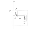
液晶表示装置の画素の一例を、図1を用いて説明する。画素100を構成する素子は、スイッチ素子として機能するトランジスタ101、及び液晶素子102である。
本実施の形態では、液晶表示装置の表示方式において、FFSモードを用いた場合について説明する。
本実施の形態では、半導体装置の作製方法の一例について、図9を用いて説明する。
本実施の形態では、先の実施の形態で得られる表示装置を搭載した電子機器の一例を図10に示す。
101 トランジスタ
102 液晶素子
103 配線
104 配線
105 ノード
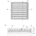
200 基板
201 電極
202 絶縁膜
203 電極
204 液晶層
205 液晶
206 容量素子
207 スリット
301 電極
303 電極
310 スリット
400 トランジスタ
401 ゲート電極
402 ゲート絶縁膜
403 酸化物半導体層
404 電極
405 電極
410 基板
1000 基板
1001 ゲート電極
1002 ゲート絶縁膜
1003 酸化物半導体膜
1004 酸化物半導体層
1005 ソース電極
1006 ドレイン電極
1007 酸化物絶縁膜
1008 トランジスタ
1009 保護絶縁膜
5000 画素
5001 トランジスタ
5002 液晶素子
5003 容量素子
5004 配線
5101 破線
5102 破線
5103 実線
5104 実線
2001〜2006 本体
2101〜2108 表示部
Claims (8)
- トランジスタと、前記トランジスタのソース又はドレインに電気的に接続された液晶素子とが設けられた画素を有し、
前記トランジスタは、半導体材料として酸化物半導体が用いられており、
前記画素には、容量素子が設けられていないことを特徴とする表示装置。 - トランジスタと、前記トランジスタのソース又はドレインに電気的に接続された液晶素子とが設けられた画素を有し、
前記トランジスタは、半導体材料として真性又は実質的に真性な酸化物半導体が用いられており、
前記画素には、容量素子が設けられていないことを特徴とする表示装置。 - トランジスタと、前記トランジスタのソース又はドレインに電気的に接続された液晶素子とが設けられた画素を有し、
前記トランジスタは、半導体材料として真性又は実質的に真性な酸化物半導体が用いられており、且つオフ電流が1×10⁻¹⁷A/μm以下であり、
前記画素には、容量素子が設けられていないことを特徴とする表示装置。 - 請求項1乃至請求項3のいずれか一において、
前記液晶素子には、ビデオ信号が入力される前に前記ビデオ信号の電圧以上の電圧が入力されることを特徴とする表示装置。 - トランジスタと、
前記トランジスタのソース又はドレインに電気的に接続された第1の電極、前記第1の電極の上方に形成された液晶層、及び前記第1の電極の下方に絶縁膜を介して形成された第2の電極とが設けられた画素を有し、
前記第1の電極と第2の電極とは重なっておらず、且つ第1の電極の端部と第2の電極の端部とが一致しており、
前記トランジスタは、半導体材料として酸化物半導体が用いられており、
前記画素には、容量素子が設けられていないことを特徴とする表示装置。 - トランジスタと、
前記トランジスタのソース又はドレインに電気的に接続された第1の電極、前記第1の電極の上方に形成された液晶層、及び前記第1の電極の下方に絶縁膜を介して形成された第2の電極とが設けられた画素を有し、
前記第1の電極と第2の電極とは重なっておらず、且つ第1の電極の端部と第2の電極の端部とが一致しており、
前記トランジスタは、半導体材料として真性又は実質的に真性な酸化物半導体が用いられており、
前記画素には、容量素子が設けられていないことを特徴とする表示装置。 - トランジスタと、
前記トランジスタのソース又はドレインに電気的に接続された第1の電極、前記第1の電極の上方に形成された液晶層、及び前記第1の電極の下方に絶縁膜を介して形成された第2の電極とが設けられた画素を有し、
前記第1の電極と第2の電極とは重なっておらず、且つ第1の電極の端部と第2の電極の端部とが一致しており、
前記トランジスタは、半導体材料として真性又は実質的に真性な酸化物半導体が用いられており、且つオフ電流が1×10⁻¹⁷A/μm以下であり、
前記画素には、容量素子が設けられていないことを特徴とする表示装置。 - 請求項4乃至請求項7のいずれか一において、
前記第1の電極には、ビデオ信号が入力される前に前記ビデオ信号以上の電圧が入力されることを特徴とする表示装置。
Priority Applications (1)
| Application Number | Priority Date | Filing Date | Title |
|---|---|---|---|
| JP2010268889A JP2011138118A (ja) | 2009-12-04 | 2010-12-02 | 表示装置 |
Applications Claiming Priority (3)
| Application Number | Priority Date | Filing Date | Title |
|---|---|---|---|
| JP2009276374 | 2009-12-04 | ||
| JP2009276374 | 2009-12-04 | ||
| JP2010268889A JP2011138118A (ja) | 2009-12-04 | 2010-12-02 | 表示装置 |
Related Child Applications (2)
| Application Number | Title | Priority Date | Filing Date |
|---|---|---|---|
| JP2015024829A Division JP2015097295A (ja) | 2009-12-04 | 2015-02-11 | 表示装置 |
| JP2015044278A Division JP6113211B2 (ja) | 2009-12-04 | 2015-03-06 | 液晶表示装置 |
Publications (2)
| Publication Number | Publication Date |
|---|---|
| JP2011138118A true JP2011138118A (ja) | 2011-07-14 |
| JP2011138118A5 JP2011138118A5 (ja) | 2014-01-23 |
Family
ID=44081694
Family Applications (6)
| Application Number | Title | Priority Date | Filing Date |
|---|---|---|---|
| JP2010268889A Withdrawn JP2011138118A (ja) | 2009-12-04 | 2010-12-02 | 表示装置 |
| JP2015024829A Withdrawn JP2015097295A (ja) | 2009-12-04 | 2015-02-11 | 表示装置 |
| JP2015044278A Active JP6113211B2 (ja) | 2009-12-04 | 2015-03-06 | 液晶表示装置 |
| JP2017048269A Active JP6379244B2 (ja) | 2009-12-04 | 2017-03-14 | 液晶表示装置 |
| JP2018142348A Withdrawn JP2018169631A (ja) | 2009-12-04 | 2018-07-30 | 表示装置 |
| JP2020126606A Withdrawn JP2020188278A (ja) | 2009-12-04 | 2020-07-27 | 表示装置 |
Family Applications After (5)
| Application Number | Title | Priority Date | Filing Date |
|---|---|---|---|
| JP2015024829A Withdrawn JP2015097295A (ja) | 2009-12-04 | 2015-02-11 | 表示装置 |
| JP2015044278A Active JP6113211B2 (ja) | 2009-12-04 | 2015-03-06 | 液晶表示装置 |
| JP2017048269A Active JP6379244B2 (ja) | 2009-12-04 | 2017-03-14 | 液晶表示装置 |
| JP2018142348A Withdrawn JP2018169631A (ja) | 2009-12-04 | 2018-07-30 | 表示装置 |
| JP2020126606A Withdrawn JP2020188278A (ja) | 2009-12-04 | 2020-07-27 | 表示装置 |
Country Status (5)
| Country | Link |
|---|---|
| US (2) | US8482005B2 (ja) |
| JP (6) | JP2011138118A (ja) |
| KR (2) | KR101800038B1 (ja) |
| TW (1) | TWI570490B (ja) |
| WO (1) | WO2011068021A1 (ja) |
Cited By (7)
| Publication number | Priority date | Publication date | Assignee | Title |
|---|---|---|---|---|
| WO2013122187A1 (ja) * | 2012-02-17 | 2013-08-22 | シャープ株式会社 | 液晶表示パネル |
| WO2013190882A1 (ja) * | 2012-06-19 | 2013-12-27 | シャープ株式会社 | 金属酸化物トランジスタ |
| JP2014032398A (ja) * | 2012-07-11 | 2014-02-20 | Semiconductor Energy Lab Co Ltd | 液晶表示装置、液晶表示装置の駆動方法 |
| JP2014095894A (ja) * | 2012-10-12 | 2014-05-22 | Semiconductor Energy Lab Co Ltd | 液晶表示装置及びその駆動方法 |
| JP2014095897A (ja) * | 2012-10-12 | 2014-05-22 | Semiconductor Energy Lab Co Ltd | 液晶表示装置 |
| US9366896B2 (en) | 2012-10-12 | 2016-06-14 | Semiconductor Energy Laboratory Co., Ltd. | Liquid crystal display device and touch panel |
| JP2022095623A (ja) * | 2013-08-23 | 2022-06-28 | 株式会社半導体エネルギー研究所 | 半導体装置 |
Families Citing this family (10)
| Publication number | Priority date | Publication date | Assignee | Title |
|---|---|---|---|---|
| CN102598280B (zh) * | 2009-10-21 | 2016-05-18 | 株式会社半导体能源研究所 | 液晶显示器件及包括该液晶显示器件的电子设备 |
| KR102078253B1 (ko) | 2010-02-26 | 2020-04-02 | 가부시키가이샤 한도오따이 에네루기 켄큐쇼 | 액정 표시 장치 |
| KR20180088759A (ko) | 2010-07-27 | 2018-08-06 | 가부시키가이샤 한도오따이 에네루기 켄큐쇼 | 반도체 장치 및 그 제작 방법 |
| US8928643B2 (en) * | 2011-02-03 | 2015-01-06 | Ernst Lueder | Means and circuit to shorten the optical response time of liquid crystal displays |
| TWI681233B (zh) | 2012-10-12 | 2020-01-01 | 日商半導體能源研究所股份有限公司 | 液晶顯示裝置、觸控面板及液晶顯示裝置的製造方法 |
| US10416504B2 (en) | 2013-05-21 | 2019-09-17 | Semiconductor Energy Laboratory Co., Ltd. | Liquid crystal display device |
| TWI636309B (zh) | 2013-07-25 | 2018-09-21 | 日商半導體能源研究所股份有限公司 | 液晶顯示裝置及電子裝置 |
| WO2016194270A1 (ja) * | 2015-05-29 | 2016-12-08 | パナソニック液晶ディスプレイ株式会社 | 液晶表示装置 |
| WO2016194269A1 (ja) | 2015-05-29 | 2016-12-08 | パナソニック液晶ディスプレイ株式会社 | 液晶表示装置 |
| KR102370488B1 (ko) | 2016-03-15 | 2022-03-04 | 가부시키가이샤 한도오따이 에네루기 켄큐쇼 | 표시 장치, 모듈, 및 전자 기기 |
Citations (10)
| Publication number | Priority date | Publication date | Assignee | Title |
|---|---|---|---|---|
| JPH0719949A (ja) * | 1993-04-27 | 1995-01-20 | Litton Syst Inc | 光信号間の干渉を表わす電気信号を生成する光検出器および方法 |
| JPH07199149A (ja) * | 1993-12-28 | 1995-08-04 | Sharp Corp | 画像表示装置及びその駆動方法 |
| JPH08264794A (ja) * | 1995-03-27 | 1996-10-11 | Res Dev Corp Of Japan | 亜酸化銅等の金属酸化物半導体による薄膜トランジスタとpn接合を形成した金属酸化物半導体装置およびそれらの製造方法 |
| JP2003050405A (ja) * | 2000-11-15 | 2003-02-21 | Matsushita Electric Ind Co Ltd | 薄膜トランジスタアレイ、その製造方法およびそれを用いた表示パネル |
| JP2007123861A (ja) * | 2005-09-29 | 2007-05-17 | Semiconductor Energy Lab Co Ltd | 半導体装置及びその作製方法 |
| JP2008287115A (ja) * | 2007-05-18 | 2008-11-27 | Semiconductor Energy Lab Co Ltd | 液晶表示装置 |
| JP2009009081A (ja) * | 2007-06-27 | 2009-01-15 | Samsung Sdi Co Ltd | 電子映像機器 |
| JP2009021612A (ja) * | 2005-09-29 | 2009-01-29 | Semiconductor Energy Lab Co Ltd | 半導体装置及びその作製方法 |
| JP2009151292A (ja) * | 2007-11-29 | 2009-07-09 | Semiconductor Energy Lab Co Ltd | 表示装置およびその駆動方法 |
| JP2009528670A (ja) * | 2006-06-02 | 2009-08-06 | 財団法人高知県産業振興センター | 半導体機器及びその製法 |
Family Cites Families (122)
| Publication number | Priority date | Publication date | Assignee | Title |
|---|---|---|---|---|
| JP2708746B2 (ja) * | 1987-07-03 | 1998-02-04 | 三菱電機株式会社 | 液晶制御回路 |
| JP2757207B2 (ja) * | 1989-05-24 | 1998-05-25 | 株式会社リコー | 液晶表示装置 |
| US5844538A (en) | 1993-12-28 | 1998-12-01 | Sharp Kabushiki Kaisha | Active matrix-type image display apparatus controlling writing of display data with respect to picture elements |
| JPH11505377A (ja) | 1995-08-03 | 1999-05-18 | フィリップス エレクトロニクス ネムローゼ フェンノートシャップ | 半導体装置 |
| JP3625598B2 (ja) | 1995-12-30 | 2005-03-02 | 三星電子株式会社 | 液晶表示装置の製造方法 |
| JPH09321305A (ja) * | 1996-05-24 | 1997-12-12 | Sharp Corp | 薄膜トランジスタ及びそれを用いた液晶表示装置 |
| JPH11274504A (ja) * | 1998-03-20 | 1999-10-08 | Advanced Display Inc | Tftおよびその製法 |
| JP4170454B2 (ja) | 1998-07-24 | 2008-10-22 | Hoya株式会社 | 透明導電性酸化物薄膜を有する物品及びその製造方法 |
| JP2000150861A (ja) | 1998-11-16 | 2000-05-30 | Tdk Corp | 酸化物薄膜 |
| JP3276930B2 (ja) | 1998-11-17 | 2002-04-22 | 科学技術振興事業団 | トランジスタ及び半導体装置 |
| TW460731B (en) | 1999-09-03 | 2001-10-21 | Ind Tech Res Inst | Electrode structure and production method of wide viewing angle LCD |
| JP2004086226A (ja) * | 1999-10-21 | 2004-03-18 | Matsushita Electric Ind Co Ltd | 液晶表示装置 |
| JP2001201754A (ja) * | 2000-01-19 | 2001-07-27 | Matsushita Electric Ind Co Ltd | 液晶表示装置 |
| JP4089858B2 (ja) | 2000-09-01 | 2008-05-28 | 国立大学法人東北大学 | 半導体デバイス |
| KR20020038482A (ko) | 2000-11-15 | 2002-05-23 | 모리시타 요이찌 | 박막 트랜지스터 어레이, 그 제조방법 및 그것을 이용한표시패널 |
| JP3997731B2 (ja) | 2001-03-19 | 2007-10-24 | 富士ゼロックス株式会社 | 基材上に結晶性半導体薄膜を形成する方法 |
| JP2002289859A (ja) | 2001-03-23 | 2002-10-04 | Minolta Co Ltd | 薄膜トランジスタ |
| JP2002055326A (ja) * | 2001-05-28 | 2002-02-20 | Hitachi Ltd | 液晶表示装置 |
| JP3925839B2 (ja) | 2001-09-10 | 2007-06-06 | シャープ株式会社 | 半導体記憶装置およびその試験方法 |
| JP4090716B2 (ja) | 2001-09-10 | 2008-05-28 | 雅司 川崎 | 薄膜トランジスタおよびマトリクス表示装置 |
| JP4164562B2 (ja) | 2002-09-11 | 2008-10-15 | 独立行政法人科学技術振興機構 | ホモロガス薄膜を活性層として用いる透明薄膜電界効果型トランジスタ |
| US7061014B2 (en) | 2001-11-05 | 2006-06-13 | Japan Science And Technology Agency | Natural-superlattice homologous single crystal thin film, method for preparation thereof, and device using said single crystal thin film |
| JP4083486B2 (ja) | 2002-02-21 | 2008-04-30 | 独立行政法人科学技術振興機構 | LnCuO(S,Se,Te)単結晶薄膜の製造方法 |
| CN1445821A (zh) | 2002-03-15 | 2003-10-01 | 三洋电机株式会社 | ZnO膜和ZnO半导体层的形成方法、半导体元件及其制造方法 |
| JP3933591B2 (ja) | 2002-03-26 | 2007-06-20 | 淳二 城戸 | 有機エレクトロルミネッセント素子 |
| US7339187B2 (en) | 2002-05-21 | 2008-03-04 | State Of Oregon Acting By And Through The Oregon State Board Of Higher Education On Behalf Of Oregon State University | Transistor structures |
| JP2004022625A (ja) | 2002-06-13 | 2004-01-22 | Murata Mfg Co Ltd | 半導体デバイス及び該半導体デバイスの製造方法 |
| US7105868B2 (en) | 2002-06-24 | 2006-09-12 | Cermet, Inc. | High-electron mobility transistor with zinc oxide |
| US7067843B2 (en) | 2002-10-11 | 2006-06-27 | E. I. Du Pont De Nemours And Company | Transparent oxide semiconductor thin film transistors |
| US7612749B2 (en) * | 2003-03-04 | 2009-11-03 | Chi Mei Optoelectronics Corporation | Driving circuits for displays |
| JP4166105B2 (ja) | 2003-03-06 | 2008-10-15 | シャープ株式会社 | 半導体装置およびその製造方法 |
| JP2004273732A (ja) | 2003-03-07 | 2004-09-30 | Sharp Corp | アクティブマトリクス基板およびその製造方法 |
| JP4108633B2 (ja) | 2003-06-20 | 2008-06-25 | シャープ株式会社 | 薄膜トランジスタおよびその製造方法ならびに電子デバイス |
| US7262463B2 (en) | 2003-07-25 | 2007-08-28 | Hewlett-Packard Development Company, L.P. | Transistor including a deposited channel region having a doped portion |
| KR101019337B1 (ko) | 2004-03-12 | 2011-03-07 | 도꾸리쯔교세이호징 가가꾸 기쥬쯔 신꼬 기꼬 | 아몰퍼스 산화물 및 박막 트랜지스터 |
| US7297977B2 (en) | 2004-03-12 | 2007-11-20 | Hewlett-Packard Development Company, L.P. | Semiconductor device |
| US7282782B2 (en) | 2004-03-12 | 2007-10-16 | Hewlett-Packard Development Company, L.P. | Combined binary oxide semiconductor device |
| US7145174B2 (en) | 2004-03-12 | 2006-12-05 | Hewlett-Packard Development Company, Lp. | Semiconductor device |
| US7211825B2 (en) | 2004-06-14 | 2007-05-01 | Yi-Chi Shih | Indium oxide-based thin film transistors and circuits |
| US7593061B2 (en) * | 2004-06-22 | 2009-09-22 | Sarnoff Corporation | Method and apparatus for measuring and/or correcting audio/visual synchronization |
| JP2006100760A (ja) | 2004-09-02 | 2006-04-13 | Casio Comput Co Ltd | 薄膜トランジスタおよびその製造方法 |
| US7285501B2 (en) | 2004-09-17 | 2007-10-23 | Hewlett-Packard Development Company, L.P. | Method of forming a solution processed device |
| US7298084B2 (en) | 2004-11-02 | 2007-11-20 | 3M Innovative Properties Company | Methods and displays utilizing integrated zinc oxide row and column drivers in conjunction with organic light emitting diodes |
| US7791072B2 (en) | 2004-11-10 | 2010-09-07 | Canon Kabushiki Kaisha | Display |
| EP1815530B1 (en) | 2004-11-10 | 2021-02-17 | Canon Kabushiki Kaisha | Field effect transistor employing an amorphous oxide |
| US7453065B2 (en) | 2004-11-10 | 2008-11-18 | Canon Kabushiki Kaisha | Sensor and image pickup device |
| JP5053537B2 (ja) | 2004-11-10 | 2012-10-17 | キヤノン株式会社 | 非晶質酸化物を利用した半導体デバイス |
| US7829444B2 (en) | 2004-11-10 | 2010-11-09 | Canon Kabushiki Kaisha | Field effect transistor manufacturing method |
| CN101057333B (zh) | 2004-11-10 | 2011-11-16 | 佳能株式会社 | 发光器件 |
| US7601984B2 (en) | 2004-11-10 | 2009-10-13 | Canon Kabushiki Kaisha | Field effect transistor with amorphous oxide active layer containing microcrystals and gate electrode opposed to active layer through gate insulator |
| US7863611B2 (en) | 2004-11-10 | 2011-01-04 | Canon Kabushiki Kaisha | Integrated circuits utilizing amorphous oxides |
| US7579224B2 (en) | 2005-01-21 | 2009-08-25 | Semiconductor Energy Laboratory Co., Ltd. | Method for manufacturing a thin film semiconductor device |
| TWI412138B (zh) | 2005-01-28 | 2013-10-11 | Semiconductor Energy Lab | 半導體裝置,電子裝置,和半導體裝置的製造方法 |
| TWI569441B (zh) | 2005-01-28 | 2017-02-01 | 半導體能源研究所股份有限公司 | 半導體裝置,電子裝置,和半導體裝置的製造方法 |
| US7858451B2 (en) | 2005-02-03 | 2010-12-28 | Semiconductor Energy Laboratory Co., Ltd. | Electronic device, semiconductor device and manufacturing method thereof |
| US7948171B2 (en) | 2005-02-18 | 2011-05-24 | Semiconductor Energy Laboratory Co., Ltd. | Light emitting device |
| US20060197092A1 (en) | 2005-03-03 | 2006-09-07 | Randy Hoffman | System and method for forming conductive material on a substrate |
| US8681077B2 (en) | 2005-03-18 | 2014-03-25 | Semiconductor Energy Laboratory Co., Ltd. | Semiconductor device, and display device, driving method and electronic apparatus thereof |
| US7544967B2 (en) | 2005-03-28 | 2009-06-09 | Massachusetts Institute Of Technology | Low voltage flexible organic/transparent transistor for selective gas sensing, photodetecting and CMOS device applications |
| US7645478B2 (en) | 2005-03-31 | 2010-01-12 | 3M Innovative Properties Company | Methods of making displays |
| US8300031B2 (en) | 2005-04-20 | 2012-10-30 | Semiconductor Energy Laboratory Co., Ltd. | Semiconductor device comprising transistor having gate and drain connected through a current-voltage conversion element |
| JP2006344849A (ja) | 2005-06-10 | 2006-12-21 | Casio Comput Co Ltd | 薄膜トランジスタ |
| US7691666B2 (en) | 2005-06-16 | 2010-04-06 | Eastman Kodak Company | Methods of making thin film transistors comprising zinc-oxide-based semiconductor materials and transistors made thereby |
| US7402506B2 (en) | 2005-06-16 | 2008-07-22 | Eastman Kodak Company | Methods of making thin film transistors comprising zinc-oxide-based semiconductor materials and transistors made thereby |
| US7507618B2 (en) | 2005-06-27 | 2009-03-24 | 3M Innovative Properties Company | Method for making electronic devices using metal oxide nanoparticles |
| KR100711890B1 (ko) | 2005-07-28 | 2007-04-25 | 삼성에스디아이 주식회사 | 유기 발광표시장치 및 그의 제조방법 |
| JP2007059128A (ja) | 2005-08-23 | 2007-03-08 | Canon Inc | 有機el表示装置およびその製造方法 |
| JP4280736B2 (ja) | 2005-09-06 | 2009-06-17 | キヤノン株式会社 | 半導体素子 |
| JP4850457B2 (ja) | 2005-09-06 | 2012-01-11 | キヤノン株式会社 | 薄膜トランジスタ及び薄膜ダイオード |
| JP4560502B2 (ja) * | 2005-09-06 | 2010-10-13 | キヤノン株式会社 | 電界効果型トランジスタ |
| JP2007073705A (ja) | 2005-09-06 | 2007-03-22 | Canon Inc | 酸化物半導体チャネル薄膜トランジスタおよびその製造方法 |
| JP5116225B2 (ja) | 2005-09-06 | 2013-01-09 | キヤノン株式会社 | 酸化物半導体デバイスの製造方法 |
| JP2007086205A (ja) * | 2005-09-20 | 2007-04-05 | Sharp Corp | 表示パネルおよび表示装置 |
| JP5037808B2 (ja) | 2005-10-20 | 2012-10-03 | キヤノン株式会社 | アモルファス酸化物を用いた電界効果型トランジスタ、及び該トランジスタを用いた表示装置 |
| CN101577293B (zh) | 2005-11-15 | 2012-09-19 | 株式会社半导体能源研究所 | 半导体器件及其制造方法 |
| JP5395994B2 (ja) * | 2005-11-18 | 2014-01-22 | 出光興産株式会社 | 半導体薄膜、及びその製造方法、並びに薄膜トランジスタ |
| KR101212146B1 (ko) * | 2005-12-14 | 2012-12-14 | 엘지디스플레이 주식회사 | 액정표시소자 |
| TWI292281B (en) | 2005-12-29 | 2008-01-01 | Ind Tech Res Inst | Pixel structure of active organic light emitting diode and method of fabricating the same |
| US7867636B2 (en) | 2006-01-11 | 2011-01-11 | Murata Manufacturing Co., Ltd. | Transparent conductive film and method for manufacturing the same |
| JP4977478B2 (ja) | 2006-01-21 | 2012-07-18 | 三星電子株式会社 | ZnOフィルム及びこれを用いたTFTの製造方法 |
| US7576394B2 (en) | 2006-02-02 | 2009-08-18 | Kochi Industrial Promotion Center | Thin film transistor including low resistance conductive thin films and manufacturing method thereof |
| US7977169B2 (en) | 2006-02-15 | 2011-07-12 | Kochi Industrial Promotion Center | Semiconductor device including active layer made of zinc oxide with controlled orientations and manufacturing method thereof |
| JP5110803B2 (ja) * | 2006-03-17 | 2012-12-26 | キヤノン株式会社 | 酸化物膜をチャネルに用いた電界効果型トランジスタ及びその製造方法 |
| EP2924498A1 (en) | 2006-04-06 | 2015-09-30 | Semiconductor Energy Laboratory Co, Ltd. | Liquid crystal desplay device, semiconductor device, and electronic appliance |
| JP5148912B2 (ja) * | 2006-04-06 | 2013-02-20 | 株式会社半導体エネルギー研究所 | 液晶表示装置及び半導体装置、並びに電子機器 |
| KR20070101595A (ko) | 2006-04-11 | 2007-10-17 | 삼성전자주식회사 | ZnO TFT |
| US20070252928A1 (en) | 2006-04-28 | 2007-11-01 | Toppan Printing Co., Ltd. | Structure, transmission type liquid crystal display, reflection type display and manufacturing method thereof |
| JP5028033B2 (ja) | 2006-06-13 | 2012-09-19 | キヤノン株式会社 | 酸化物半導体膜のドライエッチング方法 |
| JP4999400B2 (ja) * | 2006-08-09 | 2012-08-15 | キヤノン株式会社 | 酸化物半導体膜のドライエッチング方法 |
| JP4609797B2 (ja) | 2006-08-09 | 2011-01-12 | Nec液晶テクノロジー株式会社 | 薄膜デバイス及びその製造方法 |
| JP4946286B2 (ja) * | 2006-09-11 | 2012-06-06 | 凸版印刷株式会社 | 薄膜トランジスタアレイ、それを用いた画像表示装置およびその駆動方法 |
| JP4332545B2 (ja) | 2006-09-15 | 2009-09-16 | キヤノン株式会社 | 電界効果型トランジスタ及びその製造方法 |
| JP4274219B2 (ja) | 2006-09-27 | 2009-06-03 | セイコーエプソン株式会社 | 電子デバイス、有機エレクトロルミネッセンス装置、有機薄膜半導体装置 |
| JP5164357B2 (ja) | 2006-09-27 | 2013-03-21 | キヤノン株式会社 | 半導体装置及び半導体装置の製造方法 |
| US7622371B2 (en) | 2006-10-10 | 2009-11-24 | Hewlett-Packard Development Company, L.P. | Fused nanocrystal thin film semiconductor and method |
| US7772021B2 (en) | 2006-11-29 | 2010-08-10 | Samsung Electronics Co., Ltd. | Flat panel displays comprising a thin-film transistor having a semiconductive oxide in its channel and methods of fabricating the same for use in flat panel displays |
| JP2008140684A (ja) | 2006-12-04 | 2008-06-19 | Toppan Printing Co Ltd | カラーelディスプレイおよびその製造方法 |
| KR101303578B1 (ko) | 2007-01-05 | 2013-09-09 | 삼성전자주식회사 | 박막 식각 방법 |
| US8207063B2 (en) | 2007-01-26 | 2012-06-26 | Eastman Kodak Company | Process for atomic layer deposition |
| US7947981B2 (en) * | 2007-01-30 | 2011-05-24 | Semiconductor Energy Laboratory Co., Ltd. | Display device |
| KR100851215B1 (ko) | 2007-03-14 | 2008-08-07 | 삼성에스디아이 주식회사 | 박막 트랜지스터 및 이를 이용한 유기 전계 발광표시장치 |
| US7795613B2 (en) | 2007-04-17 | 2010-09-14 | Toppan Printing Co., Ltd. | Structure with transistor |
| KR101325053B1 (ko) | 2007-04-18 | 2013-11-05 | 삼성디스플레이 주식회사 | 박막 트랜지스터 기판 및 이의 제조 방법 |
| KR20080094300A (ko) | 2007-04-19 | 2008-10-23 | 삼성전자주식회사 | 박막 트랜지스터 및 그 제조 방법과 박막 트랜지스터를포함하는 평판 디스플레이 |
| KR101334181B1 (ko) | 2007-04-20 | 2013-11-28 | 삼성전자주식회사 | 선택적으로 결정화된 채널층을 갖는 박막 트랜지스터 및 그제조 방법 |
| CN101663762B (zh) | 2007-04-25 | 2011-09-21 | 佳能株式会社 | 氧氮化物半导体 |
| WO2008136505A1 (ja) * | 2007-05-08 | 2008-11-13 | Idemitsu Kosan Co., Ltd. | 半導体デバイス及び薄膜トランジスタ、並びに、それらの製造方法 |
| KR101345376B1 (ko) | 2007-05-29 | 2013-12-24 | 삼성전자주식회사 | ZnO 계 박막 트랜지스터 및 그 제조방법 |
| US7807520B2 (en) * | 2007-06-29 | 2010-10-05 | Semiconductor Energy Laboratory Co., Ltd. | Method for manufacturing semiconductor device |
| JP2009099887A (ja) * | 2007-10-19 | 2009-05-07 | Hitachi Displays Ltd | 表示装置 |
| JP2009130209A (ja) * | 2007-11-26 | 2009-06-11 | Fujifilm Corp | 放射線撮像素子 |
| US8202365B2 (en) | 2007-12-17 | 2012-06-19 | Fujifilm Corporation | Process for producing oriented inorganic crystalline film, and semiconductor device using the oriented inorganic crystalline film |
| WO2009093625A1 (ja) * | 2008-01-23 | 2009-07-30 | Idemitsu Kosan Co., Ltd. | 電界効果型トランジスタ及びその製造方法、それを用いた表示装置、並びに半導体装置 |
| JP2009206508A (ja) * | 2008-01-31 | 2009-09-10 | Canon Inc | 薄膜トランジスタ及び表示装置 |
| JP5127485B2 (ja) * | 2008-02-01 | 2013-01-23 | 株式会社ジャパンディスプレイウェスト | 液晶表示装置 |
| JP5305696B2 (ja) * | 2008-03-06 | 2013-10-02 | キヤノン株式会社 | 半導体素子の処理方法 |
| JP2009223259A (ja) * | 2008-03-19 | 2009-10-01 | Seiko Epson Corp | 液晶駆動装置、液晶装置及びその駆動方法 |
| JP5305731B2 (ja) * | 2008-05-12 | 2013-10-02 | キヤノン株式会社 | 半導体素子の閾値電圧の制御方法 |
| JP4623179B2 (ja) | 2008-09-18 | 2011-02-02 | ソニー株式会社 | 薄膜トランジスタおよびその製造方法 |
| JP5451280B2 (ja) | 2008-10-09 | 2014-03-26 | キヤノン株式会社 | ウルツ鉱型結晶成長用基板およびその製造方法ならびに半導体装置 |
| WO2011046010A1 (en) * | 2009-10-16 | 2011-04-21 | Semiconductor Energy Laboratory Co., Ltd. | Liquid crystal display device and electronic device including the liquid crystal display device |
| CN105739209B (zh) * | 2009-11-30 | 2022-05-27 | 株式会社半导体能源研究所 | 液晶显示设备、用于驱动该液晶显示设备的方法 |
-
2010
- 2010-11-05 WO PCT/JP2010/070160 patent/WO2011068021A1/en active Application Filing
- 2010-11-05 KR KR1020127017279A patent/KR101800038B1/ko active IP Right Grant
- 2010-11-05 KR KR1020147010086A patent/KR101501420B1/ko active IP Right Grant
- 2010-12-01 US US12/957,772 patent/US8482005B2/en active Active
- 2010-12-02 JP JP2010268889A patent/JP2011138118A/ja not_active Withdrawn
- 2010-12-02 TW TW099141955A patent/TWI570490B/zh active
-
2013
- 2013-06-24 US US13/924,735 patent/US8698155B2/en active Active
-
2015
- 2015-02-11 JP JP2015024829A patent/JP2015097295A/ja not_active Withdrawn
- 2015-03-06 JP JP2015044278A patent/JP6113211B2/ja active Active
-
2017
- 2017-03-14 JP JP2017048269A patent/JP6379244B2/ja active Active
-
2018
- 2018-07-30 JP JP2018142348A patent/JP2018169631A/ja not_active Withdrawn
-
2020
- 2020-07-27 JP JP2020126606A patent/JP2020188278A/ja not_active Withdrawn
Patent Citations (11)
| Publication number | Priority date | Publication date | Assignee | Title |
|---|---|---|---|---|
| JPH0719949A (ja) * | 1993-04-27 | 1995-01-20 | Litton Syst Inc | 光信号間の干渉を表わす電気信号を生成する光検出器および方法 |
| JPH07199149A (ja) * | 1993-12-28 | 1995-08-04 | Sharp Corp | 画像表示装置及びその駆動方法 |
| JPH08264794A (ja) * | 1995-03-27 | 1996-10-11 | Res Dev Corp Of Japan | 亜酸化銅等の金属酸化物半導体による薄膜トランジスタとpn接合を形成した金属酸化物半導体装置およびそれらの製造方法 |
| JP2003050405A (ja) * | 2000-11-15 | 2003-02-21 | Matsushita Electric Ind Co Ltd | 薄膜トランジスタアレイ、その製造方法およびそれを用いた表示パネル |
| JP2007123861A (ja) * | 2005-09-29 | 2007-05-17 | Semiconductor Energy Lab Co Ltd | 半導体装置及びその作製方法 |
| JP2009021612A (ja) * | 2005-09-29 | 2009-01-29 | Semiconductor Energy Lab Co Ltd | 半導体装置及びその作製方法 |
| JP2009260378A (ja) * | 2005-09-29 | 2009-11-05 | Semiconductor Energy Lab Co Ltd | 半導体装置の作製方法 |
| JP2009528670A (ja) * | 2006-06-02 | 2009-08-06 | 財団法人高知県産業振興センター | 半導体機器及びその製法 |
| JP2008287115A (ja) * | 2007-05-18 | 2008-11-27 | Semiconductor Energy Lab Co Ltd | 液晶表示装置 |
| JP2009009081A (ja) * | 2007-06-27 | 2009-01-15 | Samsung Sdi Co Ltd | 電子映像機器 |
| JP2009151292A (ja) * | 2007-11-29 | 2009-07-09 | Semiconductor Energy Lab Co Ltd | 表示装置およびその駆動方法 |
Cited By (16)
| Publication number | Priority date | Publication date | Assignee | Title |
|---|---|---|---|---|
| US9599868B2 (en) | 2012-02-17 | 2017-03-21 | Sharp Kabushiki Kaisha | Liquid crystal display panel comprising a contact site for a pixel electrode that is wider than a line portion of a lead-out line when viewed in a plan view |
| WO2013122187A1 (ja) * | 2012-02-17 | 2013-08-22 | シャープ株式会社 | 液晶表示パネル |
| WO2013190882A1 (ja) * | 2012-06-19 | 2013-12-27 | シャープ株式会社 | 金属酸化物トランジスタ |
| JP2021006934A (ja) * | 2012-07-11 | 2021-01-21 | 株式会社半導体エネルギー研究所 | 液晶表示装置、液晶表示装置の駆動方法 |
| JP2017215615A (ja) * | 2012-07-11 | 2017-12-07 | 株式会社半導体エネルギー研究所 | 液晶表示装置、及び液晶表示装置の駆動方法 |
| US9953595B2 (en) | 2012-07-11 | 2018-04-24 | Semiconductor Energy Laboratory Co., Ltd. | Liquid crystal display device and method for driving the same |
| JP2019091041A (ja) * | 2012-07-11 | 2019-06-13 | 株式会社半導体エネルギー研究所 | 液晶表示装置、及び液晶表示装置の駆動方法 |
| JP2020008865A (ja) * | 2012-07-11 | 2020-01-16 | 株式会社半導体エネルギー研究所 | 液晶表示装置、及び液晶表示装置の駆動方法 |
| JP2014032398A (ja) * | 2012-07-11 | 2014-02-20 | Semiconductor Energy Lab Co Ltd | 液晶表示装置、液晶表示装置の駆動方法 |
| JP2022028865A (ja) * | 2012-07-11 | 2022-02-16 | 株式会社半導体エネルギー研究所 | 液晶表示装置、液晶表示装置の駆動方法 |
| JP7230159B2 (ja) | 2012-07-11 | 2023-02-28 | 株式会社半導体エネルギー研究所 | 液晶表示装置、液晶表示装置の駆動方法 |
| JP2014095897A (ja) * | 2012-10-12 | 2014-05-22 | Semiconductor Energy Lab Co Ltd | 液晶表示装置 |
| US9366896B2 (en) | 2012-10-12 | 2016-06-14 | Semiconductor Energy Laboratory Co., Ltd. | Liquid crystal display device and touch panel |
| US9449574B2 (en) | 2012-10-12 | 2016-09-20 | Semiconductor Energy Laboratory Co., Ltd. | LCD overdriving using difference between average values of groups of pixels between two frames |
| JP2014095894A (ja) * | 2012-10-12 | 2014-05-22 | Semiconductor Energy Lab Co Ltd | 液晶表示装置及びその駆動方法 |
| JP2022095623A (ja) * | 2013-08-23 | 2022-06-28 | 株式会社半導体エネルギー研究所 | 半導体装置 |
Also Published As
| Publication number | Publication date |
|---|---|
| KR101501420B1 (ko) | 2015-03-10 |
| TW201133100A (en) | 2011-10-01 |
| US20110134345A1 (en) | 2011-06-09 |
| JP2015097295A (ja) | 2015-05-21 |
| JP6379244B2 (ja) | 2018-08-22 |
| KR20140052085A (ko) | 2014-05-02 |
| US8698155B2 (en) | 2014-04-15 |
| TWI570490B (zh) | 2017-02-11 |
| JP6113211B2 (ja) | 2017-04-12 |
| WO2011068021A1 (en) | 2011-06-09 |
| JP2015111736A (ja) | 2015-06-18 |
| KR101800038B1 (ko) | 2017-11-21 |
| US20130271688A1 (en) | 2013-10-17 |
| JP2020188278A (ja) | 2020-11-19 |
| JP2018169631A (ja) | 2018-11-01 |
| US8482005B2 (en) | 2013-07-09 |
| KR20120091425A (ko) | 2012-08-17 |
| JP2017116957A (ja) | 2017-06-29 |
Similar Documents
| Publication | Publication Date | Title |
|---|---|---|
| JP6379244B2 (ja) | 液晶表示装置 | |
| US20230420570A1 (en) | Semiconductor device | |
| US8884294B2 (en) | Semiconductor device and method for manufacturing the same | |
| US8628987B2 (en) | Manufacturing methods of thin film transistor, liquid crystal display device, and semiconductor device | |
| CN102097486B (zh) | 薄膜晶体管及其制造方法以及有机电致发光设备 | |
| US8803154B2 (en) | Display device and method for manufacturing the same | |
| JP6134230B2 (ja) | 薄膜トランジスタおよび表示装置 | |
| US8642380B2 (en) | Manufacturing method of semiconductor device | |
| WO2014034872A1 (ja) | 薄膜トランジスタおよび表示装置 | |
| US9577108B2 (en) | Semiconductor device | |
| US20120132902A1 (en) | Semiconductor device and manufacturing method thereof | |
| JP2015195327A (ja) | 半導体装置 | |
| US9275875B2 (en) | Method for manufacturing semiconductor device | |
| US9748399B2 (en) | Semiconductor device and display device comprising an oxide semiconductor channel region having a different crystal orientation than source/drain regions | |
| CN107026208B (zh) | 半导体装置和半导体装置的制造方法 |
Legal Events
| Date | Code | Title | Description |
|---|---|---|---|
| A521 | Request for written amendment filed |
Free format text: JAPANESE INTERMEDIATE CODE: A523 Effective date: 20131129 |
|
| A621 | Written request for application examination |
Free format text: JAPANESE INTERMEDIATE CODE: A621 Effective date: 20131129 |
|
| A131 | Notification of reasons for refusal |
Free format text: JAPANESE INTERMEDIATE CODE: A131 Effective date: 20140916 |
|
| A521 | Request for written amendment filed |
Free format text: JAPANESE INTERMEDIATE CODE: A523 Effective date: 20140925 |
|
| A131 | Notification of reasons for refusal |
Free format text: JAPANESE INTERMEDIATE CODE: A131 Effective date: 20150203 |
|
| A521 | Request for written amendment filed |
Free format text: JAPANESE INTERMEDIATE CODE: A523 Effective date: 20150211 |
|
| A02 | Decision of refusal |
Free format text: JAPANESE INTERMEDIATE CODE: A02 Effective date: 20150407 |
|
| A521 | Request for written amendment filed |
Free format text: JAPANESE INTERMEDIATE CODE: A523 Effective date: 20150422 |
|
| A911 | Transfer to examiner for re-examination before appeal (zenchi) |
Free format text: JAPANESE INTERMEDIATE CODE: A911 Effective date: 20150608 |
|
| A912 | Re-examination (zenchi) completed and case transferred to appeal board |
Free format text: JAPANESE INTERMEDIATE CODE: A912 Effective date: 20150814 |
|
| A761 | Written withdrawal of application |
Free format text: JAPANESE INTERMEDIATE CODE: A761 Effective date: 20150828 |