EP3712294A1 - Plaque métallique pour fabriquer un masque de dépôt en phase vapeur et procédé de fabrication de plaque métallique, et masque de dépôt en phase vapeur et procédé de fabrication de masque de dépôt en phase vapeur - Google Patents
Plaque métallique pour fabriquer un masque de dépôt en phase vapeur et procédé de fabrication de plaque métallique, et masque de dépôt en phase vapeur et procédé de fabrication de masque de dépôt en phase vapeur Download PDFInfo
- Publication number
- EP3712294A1 EP3712294A1 EP18879719.5A EP18879719A EP3712294A1 EP 3712294 A1 EP3712294 A1 EP 3712294A1 EP 18879719 A EP18879719 A EP 18879719A EP 3712294 A1 EP3712294 A1 EP 3712294A1
- Authority
- EP
- European Patent Office
- Prior art keywords
- metal plate
- deposition mask
- manufacturing
- less
- pit volume
- Prior art date
- Legal status (The legal status is an assumption and is not a legal conclusion. Google has not performed a legal analysis and makes no representation as to the accuracy of the status listed.)
- Pending
Links
- 229910052751 metal Inorganic materials 0.000 title claims abstract description 349
- 239000002184 metal Substances 0.000 title claims abstract description 349
- 238000004519 manufacturing process Methods 0.000 title claims abstract description 73
- 238000000034 method Methods 0.000 title claims description 37
- 238000007740 vapor deposition Methods 0.000 title description 7
- 230000008021 deposition Effects 0.000 claims abstract description 230
- 238000007689 inspection Methods 0.000 claims abstract description 102
- 238000012937 correction Methods 0.000 claims description 37
- PXHVJJICTQNCMI-UHFFFAOYSA-N Nickel Chemical compound [Ni] PXHVJJICTQNCMI-UHFFFAOYSA-N 0.000 claims description 34
- 238000005259 measurement Methods 0.000 claims description 31
- 238000005530 etching Methods 0.000 claims description 30
- 229910000640 Fe alloy Inorganic materials 0.000 claims description 18
- 229910052759 nickel Inorganic materials 0.000 claims description 17
- 238000012545 processing Methods 0.000 claims description 16
- 238000004364 calculation method Methods 0.000 claims description 13
- 238000000151 deposition Methods 0.000 description 228
- 239000000463 material Substances 0.000 description 79
- 238000000137 annealing Methods 0.000 description 54
- 239000000758 substrate Substances 0.000 description 52
- 238000005096 rolling process Methods 0.000 description 45
- 230000009467 reduction Effects 0.000 description 39
- 239000002585 base Substances 0.000 description 21
- 239000003921 oil Substances 0.000 description 15
- 235000019592 roughness Nutrition 0.000 description 13
- 239000011347 resin Substances 0.000 description 12
- 229920005989 resin Polymers 0.000 description 12
- 230000003746 surface roughness Effects 0.000 description 12
- 239000010953 base metal Substances 0.000 description 11
- 230000000875 corresponding effect Effects 0.000 description 11
- 238000004804 winding Methods 0.000 description 11
- 238000010586 diagram Methods 0.000 description 10
- 239000007789 gas Substances 0.000 description 9
- XEEYBQQBJWHFJM-UHFFFAOYSA-N Iron Chemical compound [Fe] XEEYBQQBJWHFJM-UHFFFAOYSA-N 0.000 description 8
- 239000011261 inert gas Substances 0.000 description 8
- 238000002844 melting Methods 0.000 description 8
- 230000008018 melting Effects 0.000 description 8
- 238000012986 modification Methods 0.000 description 8
- 230000004048 modification Effects 0.000 description 8
- 238000012360 testing method Methods 0.000 description 8
- 239000002826 coolant Substances 0.000 description 7
- 230000003247 decreasing effect Effects 0.000 description 7
- 230000015572 biosynthetic process Effects 0.000 description 6
- 239000013256 coordination polymer Substances 0.000 description 6
- 238000009826 distribution Methods 0.000 description 6
- 239000007788 liquid Substances 0.000 description 6
- 230000008569 process Effects 0.000 description 6
- 230000007423 decrease Effects 0.000 description 5
- 230000014509 gene expression Effects 0.000 description 5
- 230000002093 peripheral effect Effects 0.000 description 5
- 230000002829 reductive effect Effects 0.000 description 5
- 238000000926 separation method Methods 0.000 description 5
- XKRFYHLGVUSROY-UHFFFAOYSA-N Argon Chemical compound [Ar] XKRFYHLGVUSROY-UHFFFAOYSA-N 0.000 description 4
- VEXZGXHMUGYJMC-UHFFFAOYSA-N Hydrochloric acid Chemical compound Cl VEXZGXHMUGYJMC-UHFFFAOYSA-N 0.000 description 4
- 238000005137 deposition process Methods 0.000 description 4
- 238000011161 development Methods 0.000 description 4
- 229910052742 iron Inorganic materials 0.000 description 4
- 238000005406 washing Methods 0.000 description 4
- 239000011248 coating agent Substances 0.000 description 3
- 238000000576 coating method Methods 0.000 description 3
- 230000000694 effects Effects 0.000 description 3
- 239000011368 organic material Substances 0.000 description 3
- 238000007789 sealing Methods 0.000 description 3
- 238000003466 welding Methods 0.000 description 3
- VYZAMTAEIAYCRO-UHFFFAOYSA-N Chromium Chemical compound [Cr] VYZAMTAEIAYCRO-UHFFFAOYSA-N 0.000 description 2
- UFHFLCQGNIYNRP-UHFFFAOYSA-N Hydrogen Chemical compound [H][H] UFHFLCQGNIYNRP-UHFFFAOYSA-N 0.000 description 2
- 229910001374 Invar Inorganic materials 0.000 description 2
- 229910021578 Iron(III) chloride Inorganic materials 0.000 description 2
- 239000003513 alkali Substances 0.000 description 2
- 229910045601 alloy Inorganic materials 0.000 description 2
- 239000000956 alloy Substances 0.000 description 2
- 238000004458 analytical method Methods 0.000 description 2
- 229910052786 argon Inorganic materials 0.000 description 2
- 230000008859 change Effects 0.000 description 2
- 229910052804 chromium Inorganic materials 0.000 description 2
- 239000011651 chromium Substances 0.000 description 2
- 239000010941 cobalt Substances 0.000 description 2
- 229910017052 cobalt Inorganic materials 0.000 description 2
- GUTLYIVDDKVIGB-UHFFFAOYSA-N cobalt atom Chemical compound [Co] GUTLYIVDDKVIGB-UHFFFAOYSA-N 0.000 description 2
- 238000005097 cold rolling Methods 0.000 description 2
- 230000002596 correlated effect Effects 0.000 description 2
- 238000001514 detection method Methods 0.000 description 2
- 230000003628 erosive effect Effects 0.000 description 2
- 239000011521 glass Substances 0.000 description 2
- 238000000227 grinding Methods 0.000 description 2
- 238000010438 heat treatment Methods 0.000 description 2
- 239000001257 hydrogen Substances 0.000 description 2
- 229910052739 hydrogen Inorganic materials 0.000 description 2
- 239000012535 impurity Substances 0.000 description 2
- RBTARNINKXHZNM-UHFFFAOYSA-K iron trichloride Chemical compound Cl[Fe](Cl)Cl RBTARNINKXHZNM-UHFFFAOYSA-K 0.000 description 2
- 238000005304 joining Methods 0.000 description 2
- 230000007246 mechanism Effects 0.000 description 2
- 239000000203 mixture Substances 0.000 description 2
- 230000003287 optical effect Effects 0.000 description 2
- 230000036961 partial effect Effects 0.000 description 2
- IJGRMHOSHXDMSA-UHFFFAOYSA-N Atomic nitrogen Chemical compound N#N IJGRMHOSHXDMSA-UHFFFAOYSA-N 0.000 description 1
- 239000004215 Carbon black (E152) Substances 0.000 description 1
- 229910000531 Co alloy Inorganic materials 0.000 description 1
- 229910001030 Iron–nickel alloy Inorganic materials 0.000 description 1
- QXZUUHYBWMWJHK-UHFFFAOYSA-N [Co].[Ni] Chemical compound [Co].[Ni] QXZUUHYBWMWJHK-UHFFFAOYSA-N 0.000 description 1
- -1 acryl Chemical group 0.000 description 1
- 229910052782 aluminium Inorganic materials 0.000 description 1
- XAGFODPZIPBFFR-UHFFFAOYSA-N aluminium Chemical compound [Al] XAGFODPZIPBFFR-UHFFFAOYSA-N 0.000 description 1
- 230000006399 behavior Effects 0.000 description 1
- 239000005018 casein Substances 0.000 description 1
- BECPQYXYKAMYBN-UHFFFAOYSA-N casein, tech. Chemical compound NCCCCC(C(O)=O)N=C(O)C(CC(O)=O)N=C(O)C(CCC(O)=N)N=C(O)C(CC(C)C)N=C(O)C(CCC(O)=O)N=C(O)C(CC(O)=O)N=C(O)C(CCC(O)=O)N=C(O)C(C(C)O)N=C(O)C(CCC(O)=N)N=C(O)C(CCC(O)=N)N=C(O)C(CCC(O)=N)N=C(O)C(CCC(O)=O)N=C(O)C(CCC(O)=O)N=C(O)C(COP(O)(O)=O)N=C(O)C(CCC(O)=N)N=C(O)C(N)CC1=CC=CC=C1 BECPQYXYKAMYBN-UHFFFAOYSA-N 0.000 description 1
- 235000021240 caseins Nutrition 0.000 description 1
- 239000003086 colorant Substances 0.000 description 1
- 238000004624 confocal microscopy Methods 0.000 description 1
- 230000001276 controlling effect Effects 0.000 description 1
- 238000007796 conventional method Methods 0.000 description 1
- 238000005520 cutting process Methods 0.000 description 1
- 230000018044 dehydration Effects 0.000 description 1
- 238000006297 dehydration reaction Methods 0.000 description 1
- 229910001873 dinitrogen Inorganic materials 0.000 description 1
- 238000006073 displacement reaction Methods 0.000 description 1
- 238000001035 drying Methods 0.000 description 1
- 238000010891 electric arc Methods 0.000 description 1
- 238000009499 grossing Methods 0.000 description 1
- 235000019589 hardness Nutrition 0.000 description 1
- 239000001307 helium Substances 0.000 description 1
- 229910052734 helium Inorganic materials 0.000 description 1
- SWQJXJOGLNCZEY-UHFFFAOYSA-N helium atom Chemical compound [He] SWQJXJOGLNCZEY-UHFFFAOYSA-N 0.000 description 1
- 238000005098 hot rolling Methods 0.000 description 1
- 229930195733 hydrocarbon Natural products 0.000 description 1
- 150000002430 hydrocarbons Chemical class 0.000 description 1
- 239000013067 intermediate product Substances 0.000 description 1
- 239000003350 kerosene Substances 0.000 description 1
- WPBNNNQJVZRUHP-UHFFFAOYSA-L manganese(2+);methyl n-[[2-(methoxycarbonylcarbamothioylamino)phenyl]carbamothioyl]carbamate;n-[2-(sulfidocarbothioylamino)ethyl]carbamodithioate Chemical compound [Mn+2].[S-]C(=S)NCCNC([S-])=S.COC(=O)NC(=S)NC1=CC=CC=C1NC(=S)NC(=O)OC WPBNNNQJVZRUHP-UHFFFAOYSA-L 0.000 description 1
- 235000012054 meals Nutrition 0.000 description 1
- 238000003801 milling Methods 0.000 description 1
- 238000012544 monitoring process Methods 0.000 description 1
- 150000002816 nickel compounds Chemical class 0.000 description 1
- BFDHFSHZJLFAMC-UHFFFAOYSA-L nickel(ii) hydroxide Chemical compound [OH-].[OH-].[Ni+2] BFDHFSHZJLFAMC-UHFFFAOYSA-L 0.000 description 1
- 238000000059 patterning Methods 0.000 description 1
- 239000011295 pitch Substances 0.000 description 1
- 238000003825 pressing Methods 0.000 description 1
- 239000000047 product Substances 0.000 description 1
- 230000002441 reversible effect Effects 0.000 description 1
- 239000010731 rolling oil Substances 0.000 description 1
- 229910052710 silicon Inorganic materials 0.000 description 1
- 239000010703 silicon Substances 0.000 description 1
- 239000000126 substance Substances 0.000 description 1
- 239000002344 surface layer Substances 0.000 description 1
- 230000000930 thermomechanical effect Effects 0.000 description 1
Images


Classifications
-
- C—CHEMISTRY; METALLURGY
- C23—COATING METALLIC MATERIAL; COATING MATERIAL WITH METALLIC MATERIAL; CHEMICAL SURFACE TREATMENT; DIFFUSION TREATMENT OF METALLIC MATERIAL; COATING BY VACUUM EVAPORATION, BY SPUTTERING, BY ION IMPLANTATION OR BY CHEMICAL VAPOUR DEPOSITION, IN GENERAL; INHIBITING CORROSION OF METALLIC MATERIAL OR INCRUSTATION IN GENERAL
- C23C—COATING METALLIC MATERIAL; COATING MATERIAL WITH METALLIC MATERIAL; SURFACE TREATMENT OF METALLIC MATERIAL BY DIFFUSION INTO THE SURFACE, BY CHEMICAL CONVERSION OR SUBSTITUTION; COATING BY VACUUM EVAPORATION, BY SPUTTERING, BY ION IMPLANTATION OR BY CHEMICAL VAPOUR DEPOSITION, IN GENERAL
- C23C14/00—Coating by vacuum evaporation, by sputtering or by ion implantation of the coating forming material
- C23C14/04—Coating on selected surface areas, e.g. using masks
- C23C14/042—Coating on selected surface areas, e.g. using masks using masks
-
- G—PHYSICS
- G03—PHOTOGRAPHY; CINEMATOGRAPHY; ANALOGOUS TECHNIQUES USING WAVES OTHER THAN OPTICAL WAVES; ELECTROGRAPHY; HOLOGRAPHY
- G03F—PHOTOMECHANICAL PRODUCTION OF TEXTURED OR PATTERNED SURFACES, e.g. FOR PRINTING, FOR PROCESSING OF SEMICONDUCTOR DEVICES; MATERIALS THEREFOR; ORIGINALS THEREFOR; APPARATUS SPECIALLY ADAPTED THEREFOR
- G03F7/00—Photomechanical, e.g. photolithographic, production of textured or patterned surfaces, e.g. printing surfaces; Materials therefor, e.g. comprising photoresists; Apparatus specially adapted therefor
- G03F7/0035—Multiple processes, e.g. applying a further resist layer on an already in a previously step, processed pattern or textured surface
-
- G—PHYSICS
- G01—MEASURING; TESTING
- G01N—INVESTIGATING OR ANALYSING MATERIALS BY DETERMINING THEIR CHEMICAL OR PHYSICAL PROPERTIES
- G01N23/00—Investigating or analysing materials by the use of wave or particle radiation, e.g. X-rays or neutrons, not covered by groups G01N3/00 – G01N17/00, G01N21/00 or G01N22/00
- G01N23/20—Investigating or analysing materials by the use of wave or particle radiation, e.g. X-rays or neutrons, not covered by groups G01N3/00 – G01N17/00, G01N21/00 or G01N22/00 by using diffraction of the radiation by the materials, e.g. for investigating crystal structure; by using scattering of the radiation by the materials, e.g. for investigating non-crystalline materials; by using reflection of the radiation by the materials
- G01N23/20008—Constructional details of analysers, e.g. characterised by X-ray source, detector or optical system; Accessories therefor; Preparing specimens therefor
-
- B—PERFORMING OPERATIONS; TRANSPORTING
- B21—MECHANICAL METAL-WORKING WITHOUT ESSENTIALLY REMOVING MATERIAL; PUNCHING METAL
- B21B—ROLLING OF METAL
- B21B1/00—Metal-rolling methods or mills for making semi-finished products of solid or profiled cross-section; Sequence of operations in milling trains; Layout of rolling-mill plant, e.g. grouping of stands; Succession of passes or of sectional pass alternations
- B21B1/22—Metal-rolling methods or mills for making semi-finished products of solid or profiled cross-section; Sequence of operations in milling trains; Layout of rolling-mill plant, e.g. grouping of stands; Succession of passes or of sectional pass alternations for rolling plates, strips, bands or sheets of indefinite length
-
- C—CHEMISTRY; METALLURGY
- C21—METALLURGY OF IRON
- C21D—MODIFYING THE PHYSICAL STRUCTURE OF FERROUS METALS; GENERAL DEVICES FOR HEAT TREATMENT OF FERROUS OR NON-FERROUS METALS OR ALLOYS; MAKING METAL MALLEABLE, e.g. BY DECARBURISATION OR TEMPERING
- C21D1/00—General methods or devices for heat treatment, e.g. annealing, hardening, quenching or tempering
- C21D1/26—Methods of annealing
- C21D1/30—Stress-relieving
-
- C—CHEMISTRY; METALLURGY
- C21—METALLURGY OF IRON
- C21D—MODIFYING THE PHYSICAL STRUCTURE OF FERROUS METALS; GENERAL DEVICES FOR HEAT TREATMENT OF FERROUS OR NON-FERROUS METALS OR ALLOYS; MAKING METAL MALLEABLE, e.g. BY DECARBURISATION OR TEMPERING
- C21D1/00—General methods or devices for heat treatment, e.g. annealing, hardening, quenching or tempering
- C21D1/74—Methods of treatment in inert gas, controlled atmosphere, vacuum or pulverulent material
- C21D1/76—Adjusting the composition of the atmosphere
-
- C—CHEMISTRY; METALLURGY
- C21—METALLURGY OF IRON
- C21D—MODIFYING THE PHYSICAL STRUCTURE OF FERROUS METALS; GENERAL DEVICES FOR HEAT TREATMENT OF FERROUS OR NON-FERROUS METALS OR ALLOYS; MAKING METAL MALLEABLE, e.g. BY DECARBURISATION OR TEMPERING
- C21D6/00—Heat treatment of ferrous alloys
- C21D6/001—Heat treatment of ferrous alloys containing Ni
-
- C—CHEMISTRY; METALLURGY
- C21—METALLURGY OF IRON
- C21D—MODIFYING THE PHYSICAL STRUCTURE OF FERROUS METALS; GENERAL DEVICES FOR HEAT TREATMENT OF FERROUS OR NON-FERROUS METALS OR ALLOYS; MAKING METAL MALLEABLE, e.g. BY DECARBURISATION OR TEMPERING
- C21D6/00—Heat treatment of ferrous alloys
- C21D6/007—Heat treatment of ferrous alloys containing Co
-
- C—CHEMISTRY; METALLURGY
- C21—METALLURGY OF IRON
- C21D—MODIFYING THE PHYSICAL STRUCTURE OF FERROUS METALS; GENERAL DEVICES FOR HEAT TREATMENT OF FERROUS OR NON-FERROUS METALS OR ALLOYS; MAKING METAL MALLEABLE, e.g. BY DECARBURISATION OR TEMPERING
- C21D8/00—Modifying the physical properties by deformation combined with, or followed by, heat treatment
- C21D8/02—Modifying the physical properties by deformation combined with, or followed by, heat treatment during manufacturing of plates or strips
- C21D8/0221—Modifying the physical properties by deformation combined with, or followed by, heat treatment during manufacturing of plates or strips characterised by the working steps
- C21D8/0236—Cold rolling
-
- C—CHEMISTRY; METALLURGY
- C21—METALLURGY OF IRON
- C21D—MODIFYING THE PHYSICAL STRUCTURE OF FERROUS METALS; GENERAL DEVICES FOR HEAT TREATMENT OF FERROUS OR NON-FERROUS METALS OR ALLOYS; MAKING METAL MALLEABLE, e.g. BY DECARBURISATION OR TEMPERING
- C21D8/00—Modifying the physical properties by deformation combined with, or followed by, heat treatment
- C21D8/02—Modifying the physical properties by deformation combined with, or followed by, heat treatment during manufacturing of plates or strips
- C21D8/0247—Modifying the physical properties by deformation combined with, or followed by, heat treatment during manufacturing of plates or strips characterised by the heat treatment
-
- C—CHEMISTRY; METALLURGY
- C21—METALLURGY OF IRON
- C21D—MODIFYING THE PHYSICAL STRUCTURE OF FERROUS METALS; GENERAL DEVICES FOR HEAT TREATMENT OF FERROUS OR NON-FERROUS METALS OR ALLOYS; MAKING METAL MALLEABLE, e.g. BY DECARBURISATION OR TEMPERING
- C21D8/00—Modifying the physical properties by deformation combined with, or followed by, heat treatment
- C21D8/02—Modifying the physical properties by deformation combined with, or followed by, heat treatment during manufacturing of plates or strips
- C21D8/0278—Modifying the physical properties by deformation combined with, or followed by, heat treatment during manufacturing of plates or strips involving a particular surface treatment
-
- C—CHEMISTRY; METALLURGY
- C21—METALLURGY OF IRON
- C21D—MODIFYING THE PHYSICAL STRUCTURE OF FERROUS METALS; GENERAL DEVICES FOR HEAT TREATMENT OF FERROUS OR NON-FERROUS METALS OR ALLOYS; MAKING METAL MALLEABLE, e.g. BY DECARBURISATION OR TEMPERING
- C21D9/00—Heat treatment, e.g. annealing, hardening, quenching or tempering, adapted for particular articles; Furnaces therefor
- C21D9/46—Heat treatment, e.g. annealing, hardening, quenching or tempering, adapted for particular articles; Furnaces therefor for sheet metals
-
- C—CHEMISTRY; METALLURGY
- C22—METALLURGY; FERROUS OR NON-FERROUS ALLOYS; TREATMENT OF ALLOYS OR NON-FERROUS METALS
- C22C—ALLOYS
- C22C38/00—Ferrous alloys, e.g. steel alloys
- C22C38/08—Ferrous alloys, e.g. steel alloys containing nickel
-
- C—CHEMISTRY; METALLURGY
- C23—COATING METALLIC MATERIAL; COATING MATERIAL WITH METALLIC MATERIAL; CHEMICAL SURFACE TREATMENT; DIFFUSION TREATMENT OF METALLIC MATERIAL; COATING BY VACUUM EVAPORATION, BY SPUTTERING, BY ION IMPLANTATION OR BY CHEMICAL VAPOUR DEPOSITION, IN GENERAL; INHIBITING CORROSION OF METALLIC MATERIAL OR INCRUSTATION IN GENERAL
- C23C—COATING METALLIC MATERIAL; COATING MATERIAL WITH METALLIC MATERIAL; SURFACE TREATMENT OF METALLIC MATERIAL BY DIFFUSION INTO THE SURFACE, BY CHEMICAL CONVERSION OR SUBSTITUTION; COATING BY VACUUM EVAPORATION, BY SPUTTERING, BY ION IMPLANTATION OR BY CHEMICAL VAPOUR DEPOSITION, IN GENERAL
- C23C14/00—Coating by vacuum evaporation, by sputtering or by ion implantation of the coating forming material
- C23C14/22—Coating by vacuum evaporation, by sputtering or by ion implantation of the coating forming material characterised by the process of coating
- C23C14/24—Vacuum evaporation
-
- C—CHEMISTRY; METALLURGY
- C23—COATING METALLIC MATERIAL; COATING MATERIAL WITH METALLIC MATERIAL; CHEMICAL SURFACE TREATMENT; DIFFUSION TREATMENT OF METALLIC MATERIAL; COATING BY VACUUM EVAPORATION, BY SPUTTERING, BY ION IMPLANTATION OR BY CHEMICAL VAPOUR DEPOSITION, IN GENERAL; INHIBITING CORROSION OF METALLIC MATERIAL OR INCRUSTATION IN GENERAL
- C23F—NON-MECHANICAL REMOVAL OF METALLIC MATERIAL FROM SURFACE; INHIBITING CORROSION OF METALLIC MATERIAL OR INCRUSTATION IN GENERAL; MULTI-STEP PROCESSES FOR SURFACE TREATMENT OF METALLIC MATERIAL INVOLVING AT LEAST ONE PROCESS PROVIDED FOR IN CLASS C23 AND AT LEAST ONE PROCESS COVERED BY SUBCLASS C21D OR C22F OR CLASS C25
- C23F1/00—Etching metallic material by chemical means
- C23F1/02—Local etching
-
- C—CHEMISTRY; METALLURGY
- C23—COATING METALLIC MATERIAL; COATING MATERIAL WITH METALLIC MATERIAL; CHEMICAL SURFACE TREATMENT; DIFFUSION TREATMENT OF METALLIC MATERIAL; COATING BY VACUUM EVAPORATION, BY SPUTTERING, BY ION IMPLANTATION OR BY CHEMICAL VAPOUR DEPOSITION, IN GENERAL; INHIBITING CORROSION OF METALLIC MATERIAL OR INCRUSTATION IN GENERAL
- C23F—NON-MECHANICAL REMOVAL OF METALLIC MATERIAL FROM SURFACE; INHIBITING CORROSION OF METALLIC MATERIAL OR INCRUSTATION IN GENERAL; MULTI-STEP PROCESSES FOR SURFACE TREATMENT OF METALLIC MATERIAL INVOLVING AT LEAST ONE PROCESS PROVIDED FOR IN CLASS C23 AND AT LEAST ONE PROCESS COVERED BY SUBCLASS C21D OR C22F OR CLASS C25
- C23F1/00—Etching metallic material by chemical means
- C23F1/10—Etching compositions
- C23F1/14—Aqueous compositions
- C23F1/16—Acidic compositions
- C23F1/28—Acidic compositions for etching iron group metals
-
- C—CHEMISTRY; METALLURGY
- C25—ELECTROLYTIC OR ELECTROPHORETIC PROCESSES; APPARATUS THEREFOR
- C25D—PROCESSES FOR THE ELECTROLYTIC OR ELECTROPHORETIC PRODUCTION OF COATINGS; ELECTROFORMING; APPARATUS THEREFOR
- C25D1/00—Electroforming
- C25D1/04—Wires; Strips; Foils
-
- C—CHEMISTRY; METALLURGY
- C25—ELECTROLYTIC OR ELECTROPHORETIC PROCESSES; APPARATUS THEREFOR
- C25D—PROCESSES FOR THE ELECTROLYTIC OR ELECTROPHORETIC PRODUCTION OF COATINGS; ELECTROFORMING; APPARATUS THEREFOR
- C25D3/00—Electroplating: Baths therefor
- C25D3/02—Electroplating: Baths therefor from solutions
- C25D3/56—Electroplating: Baths therefor from solutions of alloys
- C25D3/562—Electroplating: Baths therefor from solutions of alloys containing more than 50% by weight of iron or nickel or cobalt
-
- G—PHYSICS
- G01—MEASURING; TESTING
- G01N—INVESTIGATING OR ANALYSING MATERIALS BY DETERMINING THEIR CHEMICAL OR PHYSICAL PROPERTIES
- G01N1/00—Sampling; Preparing specimens for investigation
- G01N1/28—Preparing specimens for investigation including physical details of (bio-)chemical methods covered elsewhere, e.g. G01N33/50, C12Q
-
- G—PHYSICS
- G01—MEASURING; TESTING
- G01N—INVESTIGATING OR ANALYSING MATERIALS BY DETERMINING THEIR CHEMICAL OR PHYSICAL PROPERTIES
- G01N23/00—Investigating or analysing materials by the use of wave or particle radiation, e.g. X-rays or neutrons, not covered by groups G01N3/00 – G01N17/00, G01N21/00 or G01N22/00
- G01N23/20—Investigating or analysing materials by the use of wave or particle radiation, e.g. X-rays or neutrons, not covered by groups G01N3/00 – G01N17/00, G01N21/00 or G01N22/00 by using diffraction of the radiation by the materials, e.g. for investigating crystal structure; by using scattering of the radiation by the materials, e.g. for investigating non-crystalline materials; by using reflection of the radiation by the materials
- G01N23/20058—Measuring diffraction of electrons, e.g. low energy electron diffraction [LEED] method or reflection high energy electron diffraction [RHEED] method
-
- G—PHYSICS
- G01—MEASURING; TESTING
- G01N—INVESTIGATING OR ANALYSING MATERIALS BY DETERMINING THEIR CHEMICAL OR PHYSICAL PROPERTIES
- G01N23/00—Investigating or analysing materials by the use of wave or particle radiation, e.g. X-rays or neutrons, not covered by groups G01N3/00 – G01N17/00, G01N21/00 or G01N22/00
- G01N23/20—Investigating or analysing materials by the use of wave or particle radiation, e.g. X-rays or neutrons, not covered by groups G01N3/00 – G01N17/00, G01N21/00 or G01N22/00 by using diffraction of the radiation by the materials, e.g. for investigating crystal structure; by using scattering of the radiation by the materials, e.g. for investigating non-crystalline materials; by using reflection of the radiation by the materials
- G01N23/203—Measuring back scattering
-
- G—PHYSICS
- G03—PHOTOGRAPHY; CINEMATOGRAPHY; ANALOGOUS TECHNIQUES USING WAVES OTHER THAN OPTICAL WAVES; ELECTROGRAPHY; HOLOGRAPHY
- G03F—PHOTOMECHANICAL PRODUCTION OF TEXTURED OR PATTERNED SURFACES, e.g. FOR PRINTING, FOR PROCESSING OF SEMICONDUCTOR DEVICES; MATERIALS THEREFOR; ORIGINALS THEREFOR; APPARATUS SPECIALLY ADAPTED THEREFOR
- G03F7/00—Photomechanical, e.g. photolithographic, production of textured or patterned surfaces, e.g. printing surfaces; Materials therefor, e.g. comprising photoresists; Apparatus specially adapted therefor
- G03F7/0015—Production of aperture devices, microporous systems or stamps
-
- G—PHYSICS
- G03—PHOTOGRAPHY; CINEMATOGRAPHY; ANALOGOUS TECHNIQUES USING WAVES OTHER THAN OPTICAL WAVES; ELECTROGRAPHY; HOLOGRAPHY
- G03F—PHOTOMECHANICAL PRODUCTION OF TEXTURED OR PATTERNED SURFACES, e.g. FOR PRINTING, FOR PROCESSING OF SEMICONDUCTOR DEVICES; MATERIALS THEREFOR; ORIGINALS THEREFOR; APPARATUS SPECIALLY ADAPTED THEREFOR
- G03F7/00—Photomechanical, e.g. photolithographic, production of textured or patterned surfaces, e.g. printing surfaces; Materials therefor, e.g. comprising photoresists; Apparatus specially adapted therefor
- G03F7/002—Photomechanical, e.g. photolithographic, production of textured or patterned surfaces, e.g. printing surfaces; Materials therefor, e.g. comprising photoresists; Apparatus specially adapted therefor using materials containing microcapsules; Preparing or processing such materials, e.g. by pressure; Devices or apparatus specially designed therefor
- G03F7/0022—Devices or apparatus
- G03F7/0027—Devices or apparatus characterised by pressure means
-
- G—PHYSICS
- G03—PHOTOGRAPHY; CINEMATOGRAPHY; ANALOGOUS TECHNIQUES USING WAVES OTHER THAN OPTICAL WAVES; ELECTROGRAPHY; HOLOGRAPHY
- G03F—PHOTOMECHANICAL PRODUCTION OF TEXTURED OR PATTERNED SURFACES, e.g. FOR PRINTING, FOR PROCESSING OF SEMICONDUCTOR DEVICES; MATERIALS THEREFOR; ORIGINALS THEREFOR; APPARATUS SPECIALLY ADAPTED THEREFOR
- G03F7/00—Photomechanical, e.g. photolithographic, production of textured or patterned surfaces, e.g. printing surfaces; Materials therefor, e.g. comprising photoresists; Apparatus specially adapted therefor
- G03F7/20—Exposure; Apparatus therefor
- G03F7/2002—Exposure; Apparatus therefor with visible light or UV light, through an original having an opaque pattern on a transparent support, e.g. film printing, projection printing; by reflection of visible or UV light from an original such as a printed image
- G03F7/2008—Exposure; Apparatus therefor with visible light or UV light, through an original having an opaque pattern on a transparent support, e.g. film printing, projection printing; by reflection of visible or UV light from an original such as a printed image characterised by the reflectors, diffusers, light or heat filtering means or anti-reflective means used
-
- G—PHYSICS
- G03—PHOTOGRAPHY; CINEMATOGRAPHY; ANALOGOUS TECHNIQUES USING WAVES OTHER THAN OPTICAL WAVES; ELECTROGRAPHY; HOLOGRAPHY
- G03F—PHOTOMECHANICAL PRODUCTION OF TEXTURED OR PATTERNED SURFACES, e.g. FOR PRINTING, FOR PROCESSING OF SEMICONDUCTOR DEVICES; MATERIALS THEREFOR; ORIGINALS THEREFOR; APPARATUS SPECIALLY ADAPTED THEREFOR
- G03F7/00—Photomechanical, e.g. photolithographic, production of textured or patterned surfaces, e.g. printing surfaces; Materials therefor, e.g. comprising photoresists; Apparatus specially adapted therefor
- G03F7/20—Exposure; Apparatus therefor
- G03F7/2022—Multi-step exposure, e.g. hybrid; backside exposure; blanket exposure, e.g. for image reversal; edge exposure, e.g. for edge bead removal; corrective exposure
-
- H—ELECTRICITY
- H01—ELECTRIC ELEMENTS
- H01J—ELECTRIC DISCHARGE TUBES OR DISCHARGE LAMPS
- H01J37/00—Discharge tubes with provision for introducing objects or material to be exposed to the discharge, e.g. for the purpose of examination or processing thereof
- H01J37/30—Electron-beam or ion-beam tubes for localised treatment of objects
- H01J37/3002—Details
- H01J37/3005—Observing the objects or the point of impact on the object
-
- H—ELECTRICITY
- H05—ELECTRIC TECHNIQUES NOT OTHERWISE PROVIDED FOR
- H05B—ELECTRIC HEATING; ELECTRIC LIGHT SOURCES NOT OTHERWISE PROVIDED FOR; CIRCUIT ARRANGEMENTS FOR ELECTRIC LIGHT SOURCES, IN GENERAL
- H05B33/00—Electroluminescent light sources
- H05B33/10—Apparatus or processes specially adapted to the manufacture of electroluminescent light sources
-
- H—ELECTRICITY
- H10—SEMICONDUCTOR DEVICES; ELECTRIC SOLID-STATE DEVICES NOT OTHERWISE PROVIDED FOR
- H10K—ORGANIC ELECTRIC SOLID-STATE DEVICES
- H10K71/00—Manufacture or treatment specially adapted for the organic devices covered by this subclass
-
- C—CHEMISTRY; METALLURGY
- C21—METALLURGY OF IRON
- C21D—MODIFYING THE PHYSICAL STRUCTURE OF FERROUS METALS; GENERAL DEVICES FOR HEAT TREATMENT OF FERROUS OR NON-FERROUS METALS OR ALLOYS; MAKING METAL MALLEABLE, e.g. BY DECARBURISATION OR TEMPERING
- C21D2261/00—Machining or cutting being involved
-
- C—CHEMISTRY; METALLURGY
- C22—METALLURGY; FERROUS OR NON-FERROUS ALLOYS; TREATMENT OF ALLOYS OR NON-FERROUS METALS
- C22C—ALLOYS
- C22C38/00—Ferrous alloys, e.g. steel alloys
- C22C38/10—Ferrous alloys, e.g. steel alloys containing cobalt
- C22C38/105—Ferrous alloys, e.g. steel alloys containing cobalt containing Co and Ni
-
- G—PHYSICS
- G01—MEASURING; TESTING
- G01N—INVESTIGATING OR ANALYSING MATERIALS BY DETERMINING THEIR CHEMICAL OR PHYSICAL PROPERTIES
- G01N2223/00—Investigating materials by wave or particle radiation
- G01N2223/05—Investigating materials by wave or particle radiation by diffraction, scatter or reflection
- G01N2223/053—Investigating materials by wave or particle radiation by diffraction, scatter or reflection back scatter
-
- G—PHYSICS
- G01—MEASURING; TESTING
- G01N—INVESTIGATING OR ANALYSING MATERIALS BY DETERMINING THEIR CHEMICAL OR PHYSICAL PROPERTIES
- G01N2223/00—Investigating materials by wave or particle radiation
- G01N2223/05—Investigating materials by wave or particle radiation by diffraction, scatter or reflection
- G01N2223/056—Investigating materials by wave or particle radiation by diffraction, scatter or reflection diffraction
- G01N2223/0565—Investigating materials by wave or particle radiation by diffraction, scatter or reflection diffraction diffraction of electrons, e.g. LEED
-
- H—ELECTRICITY
- H10—SEMICONDUCTOR DEVICES; ELECTRIC SOLID-STATE DEVICES NOT OTHERWISE PROVIDED FOR
- H10K—ORGANIC ELECTRIC SOLID-STATE DEVICES
- H10K50/00—Organic light-emitting devices
- H10K50/10—OLEDs or polymer light-emitting diodes [PLED]
- H10K50/11—OLEDs or polymer light-emitting diodes [PLED] characterised by the electroluminescent [EL] layers
-
- H—ELECTRICITY
- H10—SEMICONDUCTOR DEVICES; ELECTRIC SOLID-STATE DEVICES NOT OTHERWISE PROVIDED FOR
- H10K—ORGANIC ELECTRIC SOLID-STATE DEVICES
- H10K59/00—Integrated devices, or assemblies of multiple devices, comprising at least one organic light-emitting element covered by group H10K50/00
-
- H—ELECTRICITY
- H10—SEMICONDUCTOR DEVICES; ELECTRIC SOLID-STATE DEVICES NOT OTHERWISE PROVIDED FOR
- H10K—ORGANIC ELECTRIC SOLID-STATE DEVICES
- H10K71/00—Manufacture or treatment specially adapted for the organic devices covered by this subclass
- H10K71/10—Deposition of organic active material
- H10K71/16—Deposition of organic active material using physical vapour deposition [PVD], e.g. vacuum deposition or sputtering
- H10K71/166—Deposition of organic active material using physical vapour deposition [PVD], e.g. vacuum deposition or sputtering using selective deposition, e.g. using a mask
Definitions
- Embodiments of the present disclosure relate to a metal plate for manufacturing a deposition mask, and a manufacturing method for the metal plate. Embodiments of the present disclosure also relate to a deposition mask and a manufacturing method for the deposition mask.
- a display device used in a portable device such as a smart phone and a tablet PC is required to have high fineness, e.g., a pixel density of 500 ppi or more.
- the portable device be applicable in the Ultra High-Definitions (UHD) reference.
- the pixel density of the display device preferably is 800 ppi or more, for example.
- a known method for forming pixels of an organic EL display device is a method which uses a deposition mask in which through-holes are formed and arranged in a desired pattern, and forms pixels in the desired pattern.
- a deposition mask is firstly brought into tight contact with a substrate for organic EL display device, and then the substrate and the deposition mask in tight contact therewith are put into a deposition apparatus so as to carry out a deposition step for depositing an organic material on the substrate. This enables formation of pixels containing the organic material on the substrate in a pattern corresponding to that of through-holes in the deposition mask.
- a known manufacturing method for deposition mask is a method in which through-holes are formed in a metal plate by etching using a photolithographic technique. For example, a first resist pattern is firstly formed on a first surface of the metal plate via exposure and development, and a second resist pattern is formed on a second surface of the metal plate via exposure and development. Then, an area of the first surface of the metal plate, which is not covered with the first resist pattern, is etched to form first recesses in the first surface of the metal plate. Thereafter, an area of the second surface of the metal plate, which is not covered with the second resist pattern, is etched to form second recesses in the second surface of the metal plate.
- the metal plate for preparing the deposition mask is prepared by, for example, rolling a base material composed of an iron alloy containing nickel.
- Patent Document 1 Japanese Patent No. 5382259
- An object of embodiments of the present disclosure is to provide a metal plate suitable for manufacturing a deposition mask.
- One embodiment of the present disclosure is a manufacturing method for a metal plate used for manufacturing a deposition mask, the metal plate including a plurality of pits located on the surface of the metal plate, and the manufacturing method comprising an inspection step of determining a quality of the metal plate based on a sum of volumes of a plurality of pits located at a portion of the surface.
- the inspection step may include a calculation step of calculating a corrected pit volume density by dividing the sum of the volumes of parts of the plurality of pits by an area of the portion of the surface, the parts being a correction distance or more away from the surface in the thickness direction of the metal plate; and a determination step where the metal plate is determined as good when the corrected pit volume density is equal to or less than a first threshold.
- the metal plate may be determined as good in the determination step when the corrected pit volume density is equal to or more than a second threshold and equal to or less than the first threshold.
- the inspection step may include a calculation step of calculating the corrected pit volume density by dividing a sum of volumes of parts of the plurality of pits located at a portion of the surface by the area of the portion of the surface, the parts being a correction distance or more away from the surface in the thickness direction of the metal plate; and a selection step where the metal plate having a corrected pit volume density of equal to or less than the first threshold is selected.
- the metal plate having a corrected pit volume density of equal to or more than the second threshold and equal to or less than the first threshold may be selected in the selection step.
- the correction distance may be 0.2 ⁇ m.
- the first threshold may be 15,000 ⁇ m 3 /mm 2 .
- the second threshold in the manufacturing method for a metal plate according to the aforementioned third to fifth aspects, may be 10 ⁇ m 3 /mm 2 .
- the calculation step may include a measurement step of measuring a depth of the pit at each position in the portion of the surface.
- the depth of the pit may be measured by using a laser microscope in the measurement step.
- an area of the portion of the surface may be 0.1 mm 2 or more.
- One embodiment of the present disclosure is a metal plate for use in manufacturing of a deposition mask, the metal plate including a plurality of pits located on a surface of the metal plate; wherein, when a sum of volumes of parts of the plurality of pits located at a portion of the surface, which the parts of the plurality of pits are 0.2 ⁇ m or more away from the surface in the thickness direction of the metal plate, is referred to as a corrected pit volume, the corrected pit volume density calculated by dividing the corrected pit volume by an area of the portion of the surface is 15,000 ⁇ m 3 /mm 2 or less; wherein the corrected pit volume is calculated based on a result for a depth of the pit located at each position of the portion of the surface, the result being measured with a laser microscope; and wherein the area of the portion of the surface is 0.1 mm 2 or more.
- the corrected pit volume density may be 10 ⁇ m 3 /mm 2 or more.
- the metal plate may be composed of an iron alloy containing nickel.
- One embodiment of the present disclosure is a manufacturing method for a deposition mask including a plurality of through-holes formed therein, the method including a step of preparing the metal plate manufactured by the manufacturing method for a metal plate described above, or the metal plate described above; and a processing step of etching the metal plate to form the through-hole in the metal plate.
- One embodiment of the present disclosure is a deposition mask, including a metal plate including a plurality of pits located on a surface; and a plurality of through-holes formed in the metal plate; wherein, when a sum of volumes of parts of a plurality of pits located at a portion of the surface, which the parts of the plurality of pits are 0.2 ⁇ m or more away from the surface in the thickness direction of the metal plate, is referred to as the corrected pit volume, the corrected pit volume density calculated by dividing the corrected pit volume by the area of the portion of the surface is 15,000 ⁇ m 3 /mm 2 or less; wherein the corrected pit volume is calculated based on a result for a depth of the pit at each position of the portion of the surface, the result being measured with a laser microscope; and wherein an area of the portion of the surface is 0.1 mm 2 or more.
- the corrected pit volume density may be 10 ⁇ m 3 /mm 2 or more.
- a metal plate suitable for manufacturing a deposition mask can be efficiently obtained.
- an embodiment of the present disclosure can be combined with other embodiment or a modification within a range without any contradiction.
- the other embodiments, or the other embodiment and the modification can also be combined within a range without any contradiction.
- the modifications can also be combined within a range without any contradiction.
- a non-disclosed other step may be conducted between the disclosed steps.
- the disclosed steps may be conducted in any order within a range without any contradiction.
- a metal plate after being rolled may have pits such as oil pits formed on the surface.
- the state of the pit in the surface of the metal plate affects the size precision and the positional precision of through-holes formed in the metal plate. For example, when the depth of a pit in the surface of the metal plate is large, the size of a through-hole formed in the metal plate will be larger than a designed value. For this reason, a technique for inspecting the state of pits in the surface of a metal plate is important.
- Known techniques for inspecting irregularities such as pit in the surface of a metal plate include a technique of determining the arithmetic average roughness (Ra) and the maximum height (Ry) of the surface.
- the arithmetic average roughness (Ra) refers to a value obtained by measuring the position of the surface of the metal plate in the thickness direction (hereinafter also referred to as "height position") at a plurality of points on a given straight line, and calculating the average thereof.
- the maximum height (Ry) refers to the difference between the maximum value and the minimum value of measurement results when the height position of the surface of the metal plate is measured at a plurality of points on a given straight line.
- the present inventors have conducted extensive studies and found that there is not necessarily a high degree of correlation between indices of surface irregularities in the conventional art, such as arithmetic average roughness (Ra), and the size precision of through-holes formed in a metal plate. For this reason, when the quality of a metal plate is determined based on the arithmetic average roughness (Ra), it is necessary to make the threshold for pass/fail determination more severe than necessary in order to prevent an erroneous determination. This leads to reduction of the yield of the metal plate.
- arithmetic average roughness Ra
- Embodiments of the present disclosure aim to provide a metal plate and a manufacturing method for the metal plate, and a deposition mask and a manufacturing method for the deposition mask, which can effectively solve such a problem.
- Fig. 1 to Fig. 28 are views illustrating embodiments of the present disclosure.
- a manufacturing method for a deposition mask for use in patterning an organic material in a desired pattern on a substrate, when an organic EL display apparatus is manufacture for example.
- the embodiments of the present disclosure can be applied to a deposition mask for various uses.
- plate is not differentiated from one another based only on the difference of terms.
- sheet is a concept including members that may be called sheets or films.
- plate plane sheet plane, film plane
- a normal direction used to the plate-like (sheet-like, film-like) member means a normal direction with respect to a plate plane (sheet surface, film surface) of the member.
- the deposition apparatus 90 may include a vapor deposition source (for example, a crucible 94), a heater 96, and a deposition mask apparatus 10 therein.
- the deposition apparatus 90 may further include a gas discharge means for making the inside of the deposition apparatus 90 into a vacuum atmosphere.
- the crucible 94 contains a deposition material 98 such as an organic luminescent material.
- the heater 96 heats the crucible 94 to evaporate the deposition material 98 under a vacuum atmosphere.
- the deposition mask apparatus 10 is arranged to face with the crucible 94.
- the deposition mask apparatus 10 may include a deposition mask 20 and a frame 15 that supports the deposition mask 20.
- the frame 15 is configured to support the deposition mask 20 in a state of being pulled in the surface direction in order to prevent the deposition mask 20 from warping.
- the deposition mask apparatus 10 is arranged in the deposition apparatus 90 such that the deposition mask 20 faces a target substrate onto which the deposition material 98 is deposited, for example, an organic EL substrate 92.
- the surface of the deposition mask 20 on the side of the organic EL substrate 92 is referred to as first surface 20a, while the surface positioned on the side opposite to the first surface 20a is referred to as second surface 20b.
- the deposition mask apparatus 10 may include a magnet 93 arranged on the surface of the organic EL substrate 92 on the side opposite to the deposition mask 20.
- the magnet 93 When the magnet 93 is provided, the magnetic force attracts the deposition mask 20 toward the side of the magnet 93, so that the deposition mask 20 can be brought into tight contact with the organic EL substrate 92.
- Fig. 3 is a plan view illustrating the deposition mask apparatus 10 viewed from the first surface 20a side of the deposition mask 20.
- the deposition mask apparatus 10 may include a plurality of deposition masks 20.
- the deposition mask 20 each may have a pair of long sides 26 and a pair of short sides 27.
- the deposition mask 20 each may have a rectangular shape.
- the deposition mask 20 each may be fixed to the frame 15 at or near the pair of short sides 27 by spot welding or the like.
- the deposition mask 20 may include a metal plate substrate in which a plurality of through-holes 25 passing through the deposition mask 20 are formed.
- the deposition material 98 that has been evaporated from the crucible 94 and arrived at the deposition mask apparatus 10 adheres to the organic EL substrate 92 through the through-holes 25 in the deposition masks 20.
- a film of the deposition material 98 can be formed on the surface of the organic EL substrate 92 in a desired pattern corresponding to the positions of the through-holes 25 of the deposition masks 20.
- Fig. 2 is a sectional view illustrating an organic EL display device 100 produced using the deposition apparatus 90 shown in Fig. 1 .
- the organic EL display device 100 include at least the organic EL substrate 92 and a pixel containing the deposition material 98 provided in a certain pattern.
- the organic EL display device 100 further include an electrode electrically connected to the pixel containing the deposition material 98 (not shown).
- the electrode is, for example, pre-provided to the organic EL substrate 92 before adhesion of the deposition material 98 to the organic EL substrate 92 by the deposition step.
- the organic EL display device 100 further include other components, such as sealing member for sealing a space around the pixel containing the deposition material 98 from the outside.
- the organic EL display device 100 shown in Fig. 2 can be an intermediate of an organic EL display device, which is produced in an intermediate stage during manufacturing of the organic EL display device.
- a deposition apparatus 90 on which the deposition mask 20 corresponding to each color is mounted is prepared, and the organic EL substrate 92 is sequentially put into each vapor deposition apparatus 90.
- This enables sequential vapor deposition of, for example, an organic luminescent material for red, an organic luminescent material for green and an organic luminescent material for blue to the organic EL substrate 92.
- the deposition process may be performed inside the deposition apparatus 90 in a high-temperature atmosphere.
- the deposition masks 20, the frame 15 and the organic EL substrate 92 which are held inside the deposition apparatus 90, are also heated.
- each of deposition mask 20, the frame 15 and the organic EL substrate 92 develop size change behaviors based on their respective thermal expansion coefficients.
- the thermal expansion coefficients of the deposition mask 20, the frame 15 and the organic EL substrate 92 largely differ from one another, positioning displacement occurs because of the difference in size change.
- the size precision and the positional precision of the deposition material to be adhered to the organic EL substrate 92 is lower.
- the thermal expansion coefficients of the deposition mask 20 and the frame 15 are preferably equivalent to the thermal expansion coefficient of the organic EL substrate 92.
- an iron alloy containing nickel can be used as a main material of the deposition mask 20 and the frame 15.
- an iron alloy containing nickel in an amount of 30% by mass and 54% by mass or less can be used as a material of the substrate constituting the deposition masks 20.
- the iron alloy containing nickel examples include an invar material containing nickel in an amount of 34% by mass or more and 38% by mass or less, a super invar material containing nickel in an amount of 30% by mass or more and 34% by mass or less and further containing cobalt, and a low thermal expansion Fe-Ni based plated alloy containing nickel in an amount of 38% by mass or more and 54% by mass or less.
- the thermal expansion coefficients of the deposition mask 20 and the frame 15 are not necessarily equivalent to the thermal expansion coefficient of the organic EL substrate 92.
- materials other than the iron alloy described above may be used as a material constituting the deposition mask 20.
- iron alloys other than the iron alloy containing nickel described above, such as iron alloys containing chromium, may be used.
- the iron alloys containing chromium which can be used include iron alloys generally known as stainless. Alloys other than iron alloys such as nickel and nickel-cobalt alloy may also be used.
- the deposition mask 20 may have a pair of ear portions (first ear portion 17a and second ear portion 17b) including a pair of short side 27 of the deposition mask 20 and an intermediate portion 18 positioned between the pair of ear portions 17a and 17b.
- the ear portions 17a and 17b will be described in detail.
- the ear portions 17a and 17b are portions of the deposition mask 20, which are fixed to the frame 15.
- the ear portions 17a and 17b are formed integrally with the intermediate portion 18.
- the ear portions 17a and 17b may be composed of a material than other than that of the intermediate portion 18. In this case, the ear portions 17a and 17b are joined to the intermediate portion 18 by welding or the like.
- the intermediate portion 18 may include at least one effective area 22 through which a through-hole 25 from the first surface 20a to the second surface 20b is formed, and a peripheral area 23 surrounding the effective area 22.
- the effective area 22 is an area of the deposition mask 20, which faces to the display area of the organic EL substrate 92.
- the intermediate portion 18 includes a plurality of effective areas 22 arranged at a determined interval along the long side 26 of the deposition mask 20.
- One effective area 22 corresponds to one display area of the organic EL display device 100.
- the organic EL display device 100 can be subjected to a step-and-repeat vapor deposition.
- One effective area 22 may correspond to a plurality of display areas.
- the effective area 22 may have a substantially quadrangular outline in plan view, more precisely, a substantially rectangular outline in plan view.
- the effective area 22 each can have a variously-shaped outline depending on the shape of the display area of the organic EL substrate 92.
- the effective area 22 each may have a circular outline.
- the effective area 22 each may have the same outline as that of the display device of a smart phone or the like.
- Fig. 4 is an enlarged plan view of the effective area 22 viewed from the second surface 20b side of the deposition mask 20.
- the plurality of through-holes 25 formed in effective areas 22 may be arranged in the effective areas 22 at predetermined pitches along two directions perpendicular to each other.
- An exemplary through-hole 25 will be described in more detail with reference mainly to Fig. 5 to Fig. 7.
- Fig. 5 to Fig. 7 are cross sectional views of the effective areas 22 in Fig. 4 along the V-V direction, the VI-VI direction, and the VII-VII, respectively.
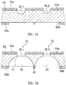
- first recesses 30 are formed in the first surface 21a of the metal plate 21, which is one side of the deposition mask 20 in the normal direction N, by an etching process, and second recesses 35 are formed in the second surface 21b of the metal plate 21, which is the other side of the deposition mask 20 in the normal direction N.
- Each of the first recesses 30 is connected to each of the second recesses 35, so that the second recess 35 and the first recess 30 are formed to communicate with each other.
- Each through-hole 25 is composed of the second recess 35 and the first recess 30 connected to the second recess 35.
- connection portion 41 is defined by a ridge line of a bulging portion where the wall surface 31 of the first recess 30, which is inclined with respect to the normal direction N of the deposition mask 20, and the wall surface 36 of the second recess 35, which is inclined with respect to the normal direction N of the deposition mask 20, are merged with each other.
- the connection portion 41 defines a through-portion 42 where an open area of the through-hole 25 is minimum in plan view of the deposition mask 20.
- the adjacent two through-holes 25 in the other side surface along the normal direction N of the deposition mask 20, i.e., in the first surface 20a of the deposition mask 20, are spaced from each other along the plate plane of the deposition mask 20.
- the first recesses 30 are made by etching the metal plate 21 from the side of the first surface 21a of the metal plate 21, which will correspond to the first surface 20a of the deposition mask 20, the first surface 21a of the metal plate 21 remains between two adjacent first recesses 30.
- the two adjacent second recesses 35 is spaced from each other along the plate plane of the deposition mask 20, on the one side along the normal direction N of the deposition mask 20, i.e., on the side of the second surface 20b of the deposition mask 20.
- the second surface 21b of the metal plate 21 remains between two adjacent second recesses 35.
- a portion of the effective area 22 of the second surface 21b of the meal plate 21, which has not been etched and thus remains, is also referred to as top portion 43.
- the deposition mask 20 is preferably produced such that the width ⁇ of the top portion 43 is not excessively large.
- the width ⁇ of the top portion 43 is preferably 2 ⁇ m or less.
- the width ⁇ of the top portion 43 varies depending on the direction along which the deposition mask 20 is cut.
- the widths ⁇ of the top portion 43 shown in Fig. 5 to Fig. 7 may differ from each other.
- the deposition mask 20 may be formed such that the width ⁇ of the top portion 43 is 2 ⁇ m or less, regardless of the direction along which the deposition mask 20 is cut.
- the shadow is a phenomenon where adhering of a deposition material to an area of a deposition target such as the organic EL substrate 92, which the area overlaps with a through-hole of the deposition mask 20, is inhibited by the second surface 20b or the wall surface of the deposition mask 20.
- the first surface 20a of the deposition mask 20 faces to the organic EL substrate 92 as shown by the two-dot chain lines in Fig. 5 , while the second surface 20b of the deposition mask 20 is located on the side of the crucible 94 holding the deposition material 98.
- the deposition material 98 adheres to the organic EL substrate 92 through the second recess 35 whose open area gradually decreases. As shown by the arrow in Fig.
- the deposition material 98 not only moves from the crucible 94 toward the organic EL substrate 92 along the normal direction N of the organic EL substrate 92, but also sometimes moves along a direction largely inclined with respect to the normal direction N of the organic EL substrate 92.
- the deposition material 98 moving at an angle is likely to be caught by the top portion 43, the wall surface 36 of the second recess 35, and the wall surface 31 of the first recess 30, so that the proportion of the deposition material 98 which fails to pass through the through-hole 25 increases.
- the thickness t of the deposition mask 20 is reduced so that the heights of the wall surface 36 of the second recess 35 and the wall surface 31 of the first recess 30 are reduced.
- a metal plate 21 having as small a thickness t as possible within a range ensuring the strength of the deposition mask 20 is used as the metal plate 21 for forming the deposition mask 20.
- the thickness t of the deposition mask 20 in the present embodiment is, for example, 30 ⁇ m or less, preferably 25 ⁇ m or less, more preferably 20 ⁇ m or less.
- the thickness t of the deposition mask 20 may be 18 ⁇ m or less, or 15 ⁇ m or less. However, when the thickness of the deposition mask 20 is too small, the strength of the deposition mask 20 decreases, so that the deposition mask 20 is likely to be damaged or deformed. In consideration of this point, the thickness t of the deposition mask 20 may be 5 ⁇ m or more, 7 ⁇ m or more, 10 ⁇ m or more, 13 ⁇ m or more, or 15 ⁇ m or more.
- the thickness t is the thickness of the peripheral area 23, i.e., the thickness of a portion of the deposition mask 20 where the first recess 30 and the second recess 35 are not formed. Therefore, the thickness t can be said as the thickness of the metal plate 21.
- the range of the thickness t of the deposition mask 20 may be defined by a combination of any one of the upper limit candidates described above and any one of the lower limit candidates described above.
- the thickness t of the deposition mask 20 may be 5 ⁇ m or more and 30 ⁇ m or less, 7 ⁇ m or more and 25 ⁇ m or less, 10 ⁇ m or more and 20 ⁇ m or less, or 13 ⁇ m or more and 18 ⁇ m or less.
- the range of the thickness t of the deposition mask 20 may be defined by a combination of any two of the upper limit candidates described above.
- the thickness t of the deposition mask 20 may be 25 ⁇ m or more and 300 ⁇ m or less.
- the range of the thickness t of the deposition mask 20 may be defined by a combination of any two of the lower limit candidates described above.
- the thickness t of the deposition mask 20 may be 5 ⁇ m or more and 7 ⁇ m or less.
- a minimum angle defined by a line L1 which passes through the connection portion 41 having the minimum open area of the through-hole 25 and another given position of the wall surface 36 of the second recess 35, with respect to the normal direction N of the deposition mask 20, is represented by a symbol ⁇ 1.
- the angle ⁇ 1 is increased.
- it is effective to reduce the above-described width ⁇ of the top portion 43, as well as to reduce the thickness t of the deposition mask 20.
- the symbol ⁇ represents a width of a portion of the effective area 22 of the first surface 21a of the metal plate 21, which has not been etched and thus remains (hereinafter also referred to as "rib portion").
- the width ⁇ of the rib portion and the size r 2 of the through-portion 42 are suitably determined depending on the size of the organic EL display device and its display pixels.
- the width ⁇ of the rib portion is 5 ⁇ m or more and 40 ⁇ m or less, while the size r 2 of the through-portion 42 is 10 ⁇ m or more and 60 ⁇ m or less.
- the width ⁇ of the rib portion may be 10 ⁇ m or more, 15 ⁇ m or more, or 20 ⁇ m or more.
- the width ⁇ of the rib portion may be 35 ⁇ m or less, 30 ⁇ m or less, or 25 ⁇ m or less.
- the range of the width ⁇ of the rib portion may be defined by a combination of any one of the upper limit candidates described above and any one of the lower limit candidates described above.
- the width ⁇ of the rib portion may be 10 ⁇ m or more and 35 ⁇ m or less, 15 ⁇ m or more and 30 ⁇ m or less, or 20 ⁇ m or more and 25 ⁇ m or less.
- the range of the width ⁇ of the rib portion may be defined by a combination of any two of the upper limit candidates described above.
- the width ⁇ of the rib portion may be 35 ⁇ m or more and 40 ⁇ m or less.
- the range of the width ⁇ of the rib portion may be defined by a combination of any two of the lower limit candidates described above.
- the width ⁇ of the rib portion may be 5 ⁇ m or more and 10 ⁇ m or less.
- the size r 2 of the through-portion 42 may be 15 ⁇ m or more, 20 ⁇ m or more, 25 ⁇ m or more, or 30 ⁇ m or more.
- the lower limit of the size r 2 of the through-portion 42 may be less than 10 ⁇ m described above.
- the size r of the through-portion 42 is 5 ⁇ m or more.
- the size r 2 of the through-portion 42 may also be 55 ⁇ m or less, 50 ⁇ m or less, 45 ⁇ m or less, 40 ⁇ m or less, or 35 ⁇ m or less.
- the range of the size r 2 of the through-portion 42 may be defined by a combination of any one of the upper limit candidates described above and any one of the lower limit candidates described above.
- the size r 2 of the through-portion 42 may be 15 ⁇ m or more and 55 ⁇ m or less, 20 ⁇ m or more and 50 ⁇ m or less, 25 ⁇ m or more and 45 ⁇ m or less, 30 ⁇ m or more and 40 ⁇ m or less, or 30 ⁇ m or more and 35 ⁇ m or less.
- the range of the size r 2 of the through-portion 42 may be defined by a combination of any two of the upper limit candidates described above.
- the size r 2 of the through-portion 42 may be 55 ⁇ m or more and 60 ⁇ m or less.
- the range of the size r 2 of the through-portion 42 may be defined by a combination of any two of the lower limit candidates described above.
- the size r 2 of the through-portion 42 may be 5 ⁇ m or more and 10 ⁇ m or less.
- Fig. 8 is a sectional view of the effective area 22 along the IX-IX direction in Fig. 8 .
- the deposition mask 20 according to the present embodiment is particularly effective when an organic EL display device having a pixel density of 450 ppi or more is produced.
- an exemplary size of the deposition mask 20 required for producing an organic EL display device having such a high pixel density is described with reference to Fig. 10.
- Fig. 10 is an enlarged sectional view showing the through-hole 25 of the deposition mask 20 shown in Fig. 5 and an area near thereto.
- a distance from the first surface 20a to the connection portion 41 of the deposition mask 20 along the normal direction N of the deposition mask 20, i.e., the height of the wall surface 31 of the first recess 30, is represented by a symbol r 1 .
- the size of the first recess 30 in a portion where the first recess 30 is connected to the second recess 35, i.e., the size of the through-portion 42 is represented by a symbol r 2 .
- an angle that is defined by a line L 2 , which connects the connection portion 41 and a distal edge of the first recess 30 in the first surface 21b of the metal plate 21, with respect to the normal line N of the metal plate 21, is represented by a symbol ⁇ 2.
- the size r 2 of the through-portion 42 is preferably set as 10 ⁇ m or more and 60 ⁇ m or less.
- a deposition mask 20 can be provided, by which an organic EL display device having a high pixel density can be produced.
- the height r 1 of the wall surface 31 of the first recess 30 is set as 6 mm or less.
- the angle ⁇ 2 corresponds to the maximum inclined angle of a deposition material 98 that can reach the organic EL substrate 92, out of deposition materials 98 that comes in an inclined manner with respect to the normal direction N of the metal plate 21 and passes through the through-portion 42 near the connection portion 41. This is because the deposition material 98 coming through the connection portion 41 at an inclined angle greater than the angle ⁇ 2 adheres to the wall surface 31 of the first recess 30 before reaching the organic EL substrate 92. Thus, by decreasing the angle ⁇ 2, adhering of the deposition material 98 coming at a large inclined angle and passing through the through-portion 42 to the organic EL substrate 92 can be prevented.
- Fig. 10 shows an embodiment in which the size of the first recess 30 in the first surface 21a, i.e., an opening size of the through-hole 25 in the first surface 21a is larger than the size r 2 of the first recess 30 in the connection portion 41.
- the value of the angle ⁇ 2 is a positive value in the illustrated embodiment.
- the size r 2 of the first recess 30 at the connection portion 41 may be larger than the size of the first recess 30 in the first surface 21a.
- the value of the angle ⁇ 2 may be a negative value.
- a manufacturing method for a metal plate used for manufacturing the deposition mask is described.
- a method in which the metal plate is composed of a rolled material that is an iron alloy containing nickel is described.
- the rolled material may have a thickness of 30 ⁇ m or less.
- the rolled material may contain 30% by mass or more and 38% by mass or less of nickel, 0% by mass or more and 6% by mass or less of cobalt, the balance of iron, and unavoidable impurities.
- iron, nickel and other materials are prepared.
- the materials are prepared so that the ratios of iron and nickel, with respect to the entire materials, are about 64% by weight and about 36% by weight, respectively.
- a melting step for melting the materials in a melting furnace is performed.
- the materials are melted by utilizing gas discharge such as arc discharge and mixed. This can provide a base material for the metal plate.
- the temperature during melting is set depending on the materials. For example, the temperature is 1,500°C or higher.
- the melting step may include a step of adding aluminum, manganese, silicon or the like to the melting furnace for deoxidization, dehydration, denitrification, or the like.
- the melting step may be performed in an atmosphere of an inert gas such as argon gas in a subatmospheric low-pressure condition.
- a step of removing the surface of the base material may be performed. Oxide films such as scale can be removed in this step.
- Specific examples of the removing method which can be employed include, but not limited to, a so-called grinding method in which the surface of the base material is removed on a rotating grinding wheel, and a so called milling method in which the surface of base material is removed by pressing the base material to a cutting tool.
- the step may be performed so that the base material has a uniform thickness.
- a rolling step for rolling a base material 60 composed of an iron alloy containing nickel For example, the base material 60 is transported toward a rolling apparatus 66 including a pair of reduction rolls 66a and 66b (work roll) while applying a tensile tension in the direction shown by the arrow D1.
- the base metal 60 having reached between the pair of reduction rolls 66a and 66b is rolled by the pair of reduction rolls 56a and 56b, so that the thickness of the base metal 60 is reduced and is elongated along the transport direction.
- a metal plate 64 having a thickness T0 can be obtained.
- a winding body 62 may be formed by winding up the metal plate 64 around a core 61.
- Fig. 11 only illustrates a schematic of the rolling step and does not particularly limit the specific compositions and procedure for performing the rolling step.
- the rolling step may include a hot rolling step of processing the base metal at a temperature not less than a temperature at which the crystalline orientation of the iron alloy constituting the base metal 60 changes, and a cold rolling step of processing the base metal at a temperature not more than a temperature at which the crystalline orientation of the iron alloy changes.
- the direction in which the base metal 60 or the metal plate 64 passes through between the pair of reduction rolls 66a and 66b is not limited to one direction. For example, in Fig. 11 and Fig.
- the base metal 60 or the metal plate 64 may be gradually rolled by repeatedly passing the base metal 60 or the metal plate 64 through between the pair of reduction rolls 66a and 66b in the direction from left to right in the drawings and in the direction from right to left in the drawings.
- the diameters of the reduction rolls 66a and 66b to be in contact with the base material 60 can be adjusted to control the surface roughness of the metal plate 64.
- the diameters of the reduction rolls 66a and 66b are decreased, the volumes of pits present in the surface of the metal plate 64 described later can be decreased. This allows the corrected pit volume density described later to be 15000 ⁇ m 3 /mm 2 or less, for example.
- the diameter of the reduction roll is 28 mm or more.
- the diameter of the reduction roll may be 40 mm or more, or 50 mm or more.
- the diameter of the reduction roll is 150 mm or less.
- the diameter of the reduction roll may be 120 mm or less, 100 mm or less, or 80 mm or less.
- the range of the diameter of the reduction roll may be defined by a combination of any one of the upper limit candidates and any one of the lower limit candidates.
- the diameter of the reduction roll may be 28 mm or more and 150 mm or less, or 40 mm or more and 120 mm or less.
- the range of the diameter of the reduction roll may be defined by a combination of any two of the upper limit candidates.
- the diameter of the reduction roll may be 120 mm or more and 150 mm or less.
- the range of the diameter of the reduction roll may be defined by a combination of any two of the lower limit candidates.
- the diameter of the reduction roll may be 28 mm or more and 40 mm or less.
- the diameter of the reduction roll is preferably 28 mm or more and 150 mm or less, more preferably 40 mm or more and 120 mm or less, still more preferably 50 mm or more and 100 mm or less, still more preferably 50 mm or more and 80 mm or less.
- the pressure by a rolling actuator may also be adjusted to control the shape of the metal plate 64.
- the backup roll may be adjusted as appropriate for the shape, and may be adjusted as appropriate for the position in the board width direction.
- the rolling speed i.e., the transport speed of the base material may also be adjusted. From the viewpoint of further reduction of the corrected pit volume density, the rolling speed is preferably slowed.
- the rolling speed is slowed, the amount of a coolant such as rolling oil caught between the base material 60 and the reduction rolls 66a and 66b can be decreased. This can reduce the number, area, or the like of oil pits formed on the surface of the metal plate 64.
- the rolling speed is 30 m/min or more.
- the rolling speed may be 50 m/min or more, 70 m/min or more, or 100 m/min or more.
- the rolling speed is 200 m/min or less.
- the rolling speed may be 150 m/min or less, 100 m/min or less, or 80 m/min or less.
- the rolling speed may be defined by a combination of any one of the upper limit candidates and any one of the lower limit candidates.
- the rolling speed may be 30 m/min or more and 200 m/min or less, or 50 m/min or more and 150 m/min or less.
- the range of the rolling speed may be defined by a combination of any two of the upper limit candidates.
- the rolling speed may be 150 m/min or more and 200 m/min or less, or 100 m/min or more and 150 m/min or less.
- the range of the rolling speed may be defined by a combination of any two of the lower limit candidates.
- the range of the rolling speed may be 30 m/min or more and 50 m/min or less, or 50 m/min or more and 70 m/min or less.
- the rolling speed is preferably 30 m/min or more and 200 m/min or less, more preferably 30 m/min or more and 150 m/min or less, still more preferably 30 m/min or more and 100 m/min or less, still more preferably 30 m/min or more and 80 m/min or less.
- a coolant such as kerosene or neat oil may be supplied between the base material 60 and the reduction rolls 66a and 66b. This can regulate the temperature of the base material. From the viewpoint of further reduction of the corrected pit volume density, the supply of the coolant is preferably decreased.
- An appropriate selection of the coolant can also control the number, area, or the like of oil pits or rolling seams formed on the surface of the metal plate 64.
- a neat oil can be used as the coolant.
- Neat oils have a characteristic that little increase in the viscosity during rolling occurs.
- the amount of the coolant caught between the base material 60 and the reduction rolls 66a and 66b can be decreased. This can prevent formation of oil pits on the surface of the metal plate 64.
- An appropriate selection of the surface roughness of the reduction roll can also control the number, area, or the like of oil pits or rolling seams formed on the surface of the metal plate 64.
- the surface roughness Ra of the reduction roll is 0.2 ⁇ m or less.
- the surface roughness Ra of the reduction roll may be 0.15 ⁇ m or less, 0.1 ⁇ m or less, or 0.05 ⁇ m or less.
- the surface roughness Rz of the reduction roll is 2.0 ⁇ m or less.
- the surface roughness Rx of the reduction roll may be 1.5 ⁇ m or less, 1.0 ⁇ m or less, or 0.5 ⁇ m or less.
- the surface roughness Rz of the reduction roll is 2.0 ⁇ m or less.
- the surface roughness Rz of the reduction roll may be 1.5 ⁇ m or less, 1.0 ⁇ m or less, or 0.5 ⁇ m or less.
- the surface roughnesses Ra and Rz are measured according to JIS B 0601 (2013).
- An analysis step for analyzing the quality and properties of the base material 60 or the metal plate 64 may be performed before, after or during the rolling step.
- the base material 60 or the metal plate 64 may be irradiated with a fluorescent X-ray in order to analyze the composition.
- a thermomechanical analysis (TMA) may be performed to measure the amount of thermal expansion in the base material 60 or the metal plate 64.
- an annealing step for annealing the metal plate 64 using an annealing apparatus 67 may be performed as shown in Fig. 12 .
- the annealing step may be performed while the metal plate 64 being pulled in the transport direction (longitudinal direction). Namely, the annealing step may be performed as a continuous annealing process while the metal plate being transported, instead of a batch annealing process.
- the temperature and the transport speed are preferably set so that deformation, such as breakage due to buckling, in the metal plate 64 is prevented.
- Fig. 12 illustrates an embodiment in which the metal plate 64 is transported in a horizontal direction during the annealing step, the present invention is not limited to this embodiment, and the metal plate 64 may be transported in the other direction such as vertical direction during the annealing step.
- the conditions of the annealing step are suitably set depending on, for example, the thickness and draft of the metal plate 64.
- the annealing step is performed in a temperature range of 500°C or higher and 600°C or lower for a period of time of 30 seconds or longer and 90 seconds or shorter.
- the number of seconds described above represents a time needed for the metal plate 64 to pass through the space adjusted to a predetermined temperature in the annealing apparatus 67.
- the temperature of the annealing step may be set not to cause softening of the metal plate 64.
- the lower limit of the temperature of the annealing step may be lower than 500°C described above.
- the temperature of the annealing step may be 400°C or higher, or 450°C or higher.
- the upper limit of the temperature of the annealing step may be higher than 600°C described above.
- the temperature of the annealing step may be 700°C or lower, or 650°C or lower.
- the range of the temperature of the annealing step may be defined by a combination of any one of the upper limit candidates described above and any one of the lower limit candidates described above.
- the temperature of the annealing step may be 400°C or higher and 700°C or lower, or 450°C or higher and 650°C or lower.
- the range of the temperature of the annealing step may be defined by a combination of any two of the upper limit candidates described above.
- the temperature of the annealing step may be 650°C or higher and 700°C or lower.
- the range of the temperature of the annealing step may be defined by a combination of any two of the lower limit candidates described above.
- the temperature of the annealing step may be 400°C or higher and 450°C or lower.
- the duration of the annealing step may be 40 seconds or longer, or 50 seconds or longer.
- the lower limit of the duration of the annealing step may be shorter than 30 seconds described above.
- the duration of the annealing step may be 10 seconds or longer, or 20 seconds or longer.
- the duration of the annealing step may be 80 seconds or shorter, 70 seconds or shorter, or 60 seconds or shorter.
- the upper limit of the duration of the annealing step may be longer than 90 seconds described above.
- the duration of the annealing step may be 100 seconds or shorter.
- the range of the duration of the annealing step may be defined by a combination of any one of the upper limit candidates described above and any one of the lower limit candidates described above.
- the duration of the annealing step may be 10 seconds or longer and 100 seconds or shorter, 20 seconds or longer and 90 seconds or shorter, 30 seconds or longer and 80 seconds or shorter, 40 seconds or longer and 70 seconds or shorter, or 50 seconds or longer and 60 seconds or shorter.
- the range of the duration of the annealing step may be defined by a combination of any two of the upper limit candidates described above.
- the duration of the annealing step may be 90 seconds or longer and 100 seconds or shorter.
- the range of the duration of the annealing step may be defined by a combination of any two of the lower limit candidates described above.
- the duration of the annealing step may be 10 seconds or longer and 20 seconds or shorter.
- the annealing step described above is performed in a non-reducing atmosphere or an inert gas atmosphere.
- non-reducing atmosphere means an atmosphere free of reducing gas such as hydrogen.
- free of reducing gas means that the concentration of reducing gas such as hydrogen is 10% or less.
- the concentration of reducing gas may be 8% or less, 6% or less, 4% or less, 2% or less, or 1% or less.
- inert gas atmosphere means an atmosphere where the concentration of inert gas such as argon gas, helium gas, or nitrogen gas is 90% or more.
- the concentration of inert gas may be 92% or more, 94% or more, 96% or more, 98% or more, or 99% or more.
- the annealing apparatus 67 may include a mechanism for monitoring the concentration of inert gas and a mechanism for controlling the concentration of inert gas.
- a washing step for washing the metal plate 64 may be performed before the annealing step. This can prevent adhering of foreign substances to the surface of the metal plate 64 during the annealing step.
- a hydrocarbon solution can be used as a washing solution for the washing.
- Fig. 12 illustrates an embodiment in which the annealing step is performed while the metal plate 64 being pulled in the longitudinal direction
- the present invention is not limited to this embodiment, and the annealing step may be performed with the metal plate 64 being in a state where it is wound around the core 61.
- the batch annealing process may be performed.
- the metal plate 64 may have a warping tendency corresponding to a winding diameter of the winding body 62.
- the slitting step is performed to remove a crack that may be generated at both ends of the metal plate 64 due to the rolling step.
- a phenomenon where the metal plate 64 is broken from the crack which is so-called plate incision, can be prevented.
- the widths of the portions to be slit in the slitting step may be adjusted so that the shape of the metal plate 64 after the slitting step is symmetric in the width direction.
- the slitting step may be performed before the annealing step described above.
- At least two steps of the rolling step, the annealing step and the slitting step described above may be repeated multiple times to prepare an elongated metal plate 64 having a predetermined thickness.
- an appearance inspection step for inspecting the appearance of the metal plate 64 may be performed.
- the appearance inspection step may include a step of inspecting the appearance of the metal plate 64 using an automatic inspection machine.
- the appearance inspection step may also include a step of visually inspecting the appearance of the metal plate 64.
- a shape inspection step for inspecting the shape of the metal plate 64 may be performed.
- the position of the surface of the metal plate 64 in the thickness direction may be determined within a predetermined area of the metal plate 64 using a coordinate measuring machine.
- Fig. 13 is a view showing how a plurality of pits 64c exist in the surface of the metal plate 64 obtained by rolling, for example, in the first surface 64a.
- the pit 64c is, for example, an oil pit 64e or a rolling seam 64f.
- the oil pit 64e is a recess formed in the surface of the metal plate 64 due to oil present between the base material 60 and the reduction rolls 66a and 66b.
- the pit 64c refers to a recess having a depth of 0.2 ⁇ m or more, of recesses such as oil pit 64e present in the surface of the metal plate 64.
- the density of pits 64c present in the surface of the metal plate 64 is, for example, 3 per mm 2 or more and 500 per mm 2 or less.
- the numerical value 0.2 ⁇ m is a preferable value of the correction distance dC described later.
- the size of the pit 64c in the surface direction of the metal plate 64 is, for example, 1 ⁇ m or more and 60 ⁇ m or less.
- Known techniques for inspecting irregularities such as pits 64c in the surface of the metal plate 64 include a technique of determining the arithmetic average roughness (Ra) and the maximum height (Ry) of the surface. For both of the arithmetic average roughness (Ra) and the maximum height (Ry), the position of the surface of the metal plate 64 in the thickness direction is determined at a plurality of points on a given line such as line R1 or R2 shown in Fig. 13 . As shown in Fig. 13 , the density of the pits 64c may vary depending on the place. As a result, as shown in Fig.
- the density of the pits 64c positioned on the line R2 can be significantly lower than the density of the pits 64c positioned on the line R1.
- the variation in inspection results can be relatively large.
- Fig. 14 is a view showing an exemplary cross section of the metal plate 64.
- Fig. 14 shows three types of pits.
- the pit 64c_1 located on the left side and the pit 64c_2 located at the center have the same opening diameter A.
- the wall surface of the pit 64c_1 has a shape that is convex toward the metal plate.
- the wall surface of the pit 64c_2 has a shape that is convex outward, as opposed to the pit 64c_1.
- the two pits 64c_3 located on the right side have an opening diameter A/2.
- the sum of the opening diameters of the two pits 64c_3 is the same as each of the opening diameter of the pit 64c_1 and the opening diameter of the pit 64c_2.
- the depths of the three types of pits 64c_1, 64c_2 and 64c_3 are all B.
- Ra ⁇ A ⁇ B / 2 dx
- the sizes of the through-hole 25, the first recess 30, the second recess 35, the top portion 43, the rib portion, and the like that are formed by etching of the metal plate 64 are affected not only by the depth of the pit 64c but also by the volume of the pit 64c.
- the surface roughness is evaluated based on the volume of the pit.
- the influences of the three types of pits 64c_1, 64c_2 and 64c_3 on the corrected pit volume density described later are different. Specifically, the influence of the pit 64c_1 on the corrected pit volume density is largest.
- the influence of one pit 64c_2 on the corrected pit volume density is smaller than the influence of two pits 64c_3 on the corrected pit volume density.
- Fig. 15 is a sectional view showing a step of forming the first recess 30 by etching the metal plate 64 shown in Fig. 14 with a first resist pattern 65a as a mask from the first surface 64a side.
- the volume of the pit 64c_1 on the left side is larger than that of the pit 64c_2 on the right side. Therefore, at the place where the pit 64c_1 on the left side has been present, the etching progresses in the thickness direction and the surface direction of the metal plate 64 more quickly than at the place where the pit 64c_2 on the right side has been present.
- the size of the first recess 30_1 formed at the place where the pit 64c_1 on the left side has been present is larger than the size of the first recess 30_2 formed at the place where the pit 64c_2 on the right side has been present.
- Fig. 16 is a sectional view showing a step of forming the second recesses 35 each communicating with the first recess 30_1 or 30_2 on the second surface 64b side of the metal plate 64, by etching the metal plate 64 shown in Fig. 15 with a second resist pattern 65b as a mask from the second surface 64b side. Since the size of the first recess 30_1 on the left side is larger than the size of the first recess 30_2 on the right side, the outline size of the connection portion 41 where the first recess 30_1 and the second recess 35 are connected on the left side is also larger than the outline size of the connection portion 41 where the first recessed 30_2 and the second recessed 35 are connected on the right side.
- Fig. 17 is a view for illustrating how the precision of the opening size of the through-hole 25 on the first surface 20a side is lowered due to the pit 64c in the metal plate 64.
- an etchant can enter the pit 64c at the start of the etching step. Therefore, at the place where the pit 64c has been present, the etching can progress in the thickness direction and the surface direction of the metal plate 64 more quickly than at the other position.
- the size of the through-hole 25 in the surface direction of the metal plate 64 can be increased at the portion where the pit 64c has been present.
- the size r 3 of the first recess 30 constituting the through-hole 25 on the first surface 20a can vary at the place where the pit 64c having a large volume has been present.
- a variation in the size r 2 of the through-portion 42 constituted by the connection portion 41 where the first recess 30 and the second recess 35 are connected may also occur.
- the size precision and the positional precision of the deposition material to be adhered to the organic EL substrate 92 are lowered.
- Such a variation in the opening size may also occur for the second recess 35 on the second surface 20b side.
- the inspection of the metal plate 64 be performed in consideration of the volume of the pit 64c. This enables a more accurate prediction for the degree of the reduction in the size precision of the through-holes 25 in the deposition mask 20 caused by the pits 64c. This enables the inspection of the metal plate 64 without making the threshold for pass/fail determination more severe than necessary, so that the yield of the metal plate 64 can be increased.
- an exemplary inspection step in consideration of the volume of the pit 64c will be described with reference to Fig. 18 and Fig. 19 .
- Fig. 18 is an enlarged plan view showing a portion of the first surface 64a of the metal plate 64. A plurality of pits 64c are formed on the first surface 64a.
- the symbol D1 represents the transport direction of the metal plate 64 during the rolling step (hereinafter also referred to as the first direction).
- the symbol D2 represents the direction orthogonal to the first direction D1 (hereinafter also referred to as the second direction).
- the quality of the metal plate 64 is determined based on the volumes of the plurality of pits 64c located at the inspection area 711 of the first surface 64a shown in Fig. 18 .
- the area U1 of the inspection area 711 is, for example, 0.1 mm 2 or more and 1.5 mm 2 or less.
- the area U1 of the inspection area 711 is 0.1 mm 2 or more, variation of the inspection results depending on the position of the inspection area 711 can be reduced.
- the area U1 of the inspection area 711 is 1.5 mm 2 or less, an excessive prolongation of the time required for the inspection can be prevented.
- the inspection step includes a calculation step S1 and a determination step S2.
- the calculation step S1 is for calculating the corrected pit volume density.
- the corrected pit volume density is an index having a high correlation with the size precision of the components of the deposition mask 20, as supported in the Examples described later.
- the metal plate 64 is determined to be good when the corrected pit volume density is equal to or less than a predetermined threshold.
- the calculation step S1 includes a measurement step S11 and a processing step S12.
- the measurement step S11 first, as shown in Fig. 18 , the plurality of unit area 712 are each photographed, and the depth of pits 64c is measured from the obtained image.
- the unit area 712 is, for example, a rectangular area having a side with a length W1 and a side with a length W2, as shown in Fig. 18 .
- the unit area 712 corresponds to the range of an image that can be taken in one photographing.
- the side of the length W1 is parallel to the first direction D1
- the side of the length W2 is parallel to the second direction D2.
- W1 is 270 ⁇ m
- W2 is 202 ⁇ m
- the expression “the side of the length W1 is parallel to the first direction D1” means that the angle defined by the side with a length W1 and the first direction D1 is in the range of -10° to +10°.
- the expression “the side of the length W2 is parallel to the second direction D2” means that the angle defined by the side with a length W2 and the second direction D2 is in the range of -10° to +10°.
- two or more are performed so that two adjacent unit areas 712 partially overlap in the first direction D1, and two adjacent unit areas 712 also partially overlap in the second direction D2.
- a plurality of thus-obtained images can be connected using an image connection software or the like to obtain an image of an area larger than one unit area 712.
- an area indicated by symbol 711 in Fig. 18 is extracted as an inspection area from the image obtained by connection.
- the inspection area 711 is defined to surround one unit area 712 located at the center among the nine unit areas 712 shown in Fig. 18 and to partially contain the eight unit areas 712 located around.
- An exemplary length of the inspection area 711 in the first direction D1 is 700 ⁇ m
- an exemplary length of the inspection area 711 in the second direction D2 is 500 ⁇ m.
- the symbol 713 represents a pixel corresponding to the resolution of the inspection apparatus.
- One pixel 713 corresponds to, for example, one spot of a laser irradiated to the metal plate 64 by the inspection device.
- the length W3 in the first direction D1 and the length W4 in the second direction D2 of the pixel 713 are preferably 0.1 ⁇ m or more and 0.4 ⁇ m or less.
- the area U2 of the pixel 713 is preferably 0.01 ⁇ m 2 or more and 0.2 ⁇ m 2 or less.
- the length W3 in the first direction D1 and the length W4 in the second direction D2 of the pixel 713 are both 0.263 ⁇ m.
- the area U2 of the pixel 713 is 0.069 ⁇ m 2 .
- Fig. 19 is a sectional view of a metal plate 64 on which pits 64c are formed, which is cut in parallel to the first direction D1.
- the symbol d(k) represents the distance from the first surface 64a to the bottom of the pit 64c at the pixel 713 located at the coordinate x(k) in the first direction D1.
- k is an integer, and the possible range of k is determined by the resolution of the image.
- the first surface 64a of the metal plate 64 may have fine ruggedness or irregularities in addition to the distinct pit 64c as shown in Fig 19 .
- the measurement result for the depth of the pit 64c may vary depending on the state of the first surface 64a around the pit 64c.
- the position of a reference plane RP which is a virtual plane may be adopted as the position of the first surface 64a in the thickness direction of the metal plate 64.
- the reference plane RP will be described.
- the reference plane RP of the first surface 64a is a plane estimated by, for example, least-squares method. Specifically, first, the position in the thickness direction of the inspection area 711 in the surface of the first surface 64a of the metal plate 64 is determined using a laser microscope described later. Subsequently, a given plane is temporarily set as the reference plane RP, and the square of the distance from the position of the surface of the first surface 64a to the reference plane RP is calculated in each pixel 713. In this case, a plane where the sum of each square of the distance is minimized can be adopted as the reference plane RP.
- the depth d(k) of the pit 64c is measured for each pixel 713 in the inspection area 711.
- the measurement value of the depth is the distance value from the measurement value of the position in the thickness direction of the surface of the first surface 64a of the metal plate 64 to the reference plane RP estimated by the least-squares method.
- a laser microscope can be used as an inspection apparatus used in the measurement step S11.
- the inspection area 711 in the first surface 64a of the metal plate 64 is irradiated with a laser beam.
- the image of a laser beam reflected by the inspection area 711 is obtained as a two-dimensional reflection image of the inspection area 711 using, for example, a CCD or CMOS image sensor.
- the two-dimensional reflection image is analyzed based on the principle of confocal microscopy to measure the position of each pixel 713 in the inspection area 711 in the thickness direction of the surface of the first surface 64a of the metal plate 64.
- Example of the laser microscope which can be used include laser microscope VK-X200 series produced by Keyence Corporation.
- step S12 information on the volume of the pit 64c in the inspection area 711 is calculated based on the depth of the pit 64c measured for each pixel 713 in the inspection area 711.
- a correction plane CP is first set, which is located on the second surface 64b side by a predetermined correction distance dC from the reference plane RP in the thickness direction of the metal plate 64. Subsequently, the sum of the volumes of parts of the pits 64c located at the inspection area 711 is calculated, wherein the parts are positioned on the second surface 64b side and the parts are the correction distance dC or more away from the reference plane RP in the thickness direction of the metal plate 64.
- a value d(k) - dC is calculated by subtracting the correction distance dC from the depth d(k), for a part of the pit 64c located at the inspection area 711, the part having a depth greater than the correction distance dC. Then, the value d(k) - dC is multiplied by the area U2 of the pixel 713.
- the volume V(k) ( ⁇ (d(k) - dC) ⁇ U2 ⁇ ) of a part of the pit 64c, the part located on the second surface 64b side with respect to the correction plane CP, is calculated at each pixel 713.
- the volumes V(k) are integrated over the entire inspection area 711.
- corrected pit volume V1
- the corrected pit volume V1 is divided by the area U1 of the inspection area 711.
- the corrected pit volume per unit area (hereinafter also referred to as corrected pit volume density) V2 can be calculated.
- the correction distance dC described above is preferably 0.1 ⁇ m or more and 0.5 ⁇ m or less, and is, for example, 0.2 ⁇ m.
- the correction distance dC and calculating the corrected pit volume density V2 the correlation can be enhanced between the corrected pit volume density V2 and the size precision of the components of the deposition mask 20, as supported by the Examples described later.
- the corrected pit volume V1 and the corrected pit volume density V2 obtained when the correction distance dC is set to be z ⁇ m may also referred to as the corrected pit volume V1 (z ⁇ m) and the corrected pit volume density V2 (z ⁇ m), respectively.
- the correction distance dC is 0.2 ⁇ m
- expressions "corrected pit volume V1 (0.2 ⁇ m)” and "corrected pit volume density V2 (0.2 ⁇ m)” may be used.
- a determination step S2 is performed where the metal plate 64 is determined to be good when the corrected pit volume density V2 is equal to or less than a predetermined threshold TH1.
- the metal plate 64 with which the components of the deposition mask 20 can be precisely formed, such as the through-hole 25, can be selected.
- the threshold TH1 is appropriately determined based on, for example, the size precision required for the components of the deposition mask 20, and the setting of the correction distance dC. For example, when the error in the opening size of the through-hole 25 in the deposition mask 20, such as r 3 of the first recess 30 or the size r2 of the through-portion 42 described above, is required to be ⁇ 1.0 ⁇ m or less, and the correction distance dC is 0.2 ⁇ m, then the threshold TH1 can be set to be 15,000 ⁇ m 3 /mm 2 .
- the threshold TH1 may be 12,000 ⁇ m 3 /mm 2 , 10,000 ⁇ m 3 /mm 2 , 9,000 ⁇ m 3 /mm 2 , 6,000 ⁇ m 3 /mm 2 , 5,000 ⁇ m 3 /mm 2 , 3,000 ⁇ m 3 /mm 2 , or 1,000 ⁇ m 3 /mm 2 .
- the determination step S2 may determine the metal plate 64 as good.
- the determination step S2 may employ not only the threshold TH1 defining the upper limit of the corrected pit volume density V2, but also the threshold TH2 defining the lower limit of the corrected pit volume density V2.
- the metal plate 64 has a corrected pit volume density V2 that is equal to or more than the threshold TH2
- the adherence of the resist film to the surface of the metal plate 64 can be increased.
- the upper threshold TH1 may be referred to as the first threshold
- the lower threshold TH2 may be referred to as the second threshold.
- the threshold TH2 may be 10 ⁇ m 3 /mm 2 , 100 ⁇ m 3 /mm 2 , 500 ⁇ m 3 /mm 2 , 1,000 ⁇ m 3 /mm 2 , 3,000 ⁇ m 3 /mm 2 , 4,000 ⁇ m 3 /mm 2 , or 5,000 ⁇ m 3 /mm 2 .
- the range of the corrected pit volume density V2 of the metal plate 64 determined as good in the determination step S2 may be defined by a combination of any one of the upper threshold TH1 candidates described above and any one of the lower threshold TH2 candidates described above.
- the corrected pit volume density V2 of the metal plate 64 determined as good i.e., the selected metal plate 64 may be 10 ⁇ m 3 /mm 2 or more and 15,000 ⁇ m 3 /mm 2 or less, 100 ⁇ m 3 /mm 2 or more and 12,000 ⁇ m 3 /mm 2 or less, 500 ⁇ m 3 /mm 2 or more and 10,000 ⁇ m 3 /mm 2 or less, 1,000 ⁇ m 3 /mm 2 or more and 9,000 ⁇ m 3 /mm 2 or less, 3,000 ⁇ m 3 /mm 2 or more and 6,000 ⁇ m 3 /mm 2 or less, and 4,000 ⁇ m 3 /mm 2 or more and 6,000 ⁇ m 3 /mm 2 or less.
- the range of the corrected pit volume density V2 of the selected metal plate 64 may be defined by a combination of any two of the upper threshold TH1 candidates described above.
- the corrected pit volume density V2 of the selected metal plate 64 may be 12,000 ⁇ m 3 /mm 2 or more and 15,000 ⁇ m 3 /mm 2 or less.
- the range of the corrected pit volume density V2 of the selected metal plate 64 may be defined by a combination of any two of the lower threshold TH2 candidates described above.
- the corrected pit volume density V2 of the selected metal plate 64 may be 10 ⁇ m 3 /mm 2 or more and 100 ⁇ m 3 /mm 2 or less.
- Fig. 39 is a graph showing an example of the distribution of the corrected pit volume densities V2 of a plurality of metal plates 64 selected based on a determination condition where the metal plate having a corrected pit volume density V2 equal to or less than the threshold TH1 is determined as good.
- the horizontal axis represents the value of the corrected pit volume density V2 calculated for each metal plate 64.
- the vertical axis represents the number of metal plates 64 having a corrected pit volume density V2 in the range represented by the horizontal axis. For example, the number of the metal plates 64 having a corrected pit volume density V2 of 6,000 ⁇ m 3 /mm 2 or more and less than 9,000 ⁇ m 3 /mm 2 among the plurality of selected metal plates 64 is 17.
- the threshold TH1 is 15,000 ⁇ m 3 /mm 2 .
- most, e.g., 95% or more, of the metal plates 64 determined as good have a corrected pit volume density V2 of 15,000 ⁇ m 3 /mm 2 or less.
- a part of the selected metal plates 64 may have a corrected pit volume density V2 exceeding 15,000 ⁇ m 3 /mm 2 due to a measurement error or the like.
- Fig. 40 shows an example of the distribution of the corrected pit volume density V2 of a plurality of metal plates 64 selected based on a determination condition where the metal plate having a corrected pit volume density V2 of equal to or more than the threshold TH2 and equal to or less than the threshold TH1 as good.
- the meanings of the horizontal and vertical axes shown in Fig. 40 are the same as in Fig 39 .
- the threshold TH2 is 3,000 ⁇ m 3 /mm 2
- the threshold TH1 is 15,000 ⁇ m 3 /mm 2 .
- the range of the metal plates 64 selected as good products is narrower than that of the example in Fig. 39 .
- the performance of selection as shown in Fig. 40 also include the performance of selection as shown in Fig. 39 .
- an embodiment has been shown in which an inspection step of inspecting the metal plate 64 based on the corrected pit volume density V2 is used to determine the quality of the metal plate 64, or to select the metal plate 64.
- the inspection step functions as a selection step of selecting the metal plate 64 in the manufacturing method for the metal plate 64.
- the inspection step may be used for purposes other than selection of the metal plate 64 in the manufacturing method of the metal plate 64.
- any selection conditions may be used in the selection step.
- a metal plate 64 may be selected, which has a corrected pit volume density V2 belonging within a range defined by a combination of any one of the upper threshold TH1 candidates described above and any one of the lower threshold TH2 candidates described above.
- a metal plate 64 may be selected, which has a corrected pit volume density V2 belonging within a range defined by a combination of any two of the upper threshold TH1 candidates described above.
- a metal plate 64 may be selected, which has a corrected pit volume density V2 belonging within a range defined by a combination of any two of the lower threshold TH2 candidates described above.
- the inspection step is used for the purpose other than selection of the metal plate 64 in the manufacturing method for the metal plate 64.
- the inspection step may be used for optimizing the conditions for manufacturing the metal plate 64, such as reduction ratio and oil usage.
- the inspection step may be used for operations of manufacturing the metal plates 64 with various reduction ratios and oil usages, calculating the corrected pit volume density V2 from each of the obtained metal plates 64, and determining an appropriate manufacturing conditions capable of lowering the corrected pit volume density V2.
- the selection based on the inspection step is performed for all the metal plates 64 obtained during the manufacturing process for the metal plate 64.
- the inspection step may be performed only for some of the metal plates 64. Alternatively, after a manufacturing condition has been once set, the inspection step may not be performed at all.
- Fig. 41 is a graph showing an example of the distribution of the corrected pit volume densities V2 of a plurality of metal plates 64 manufactured based on manufacturing conditions found by using a determination condition where the metal plate having a corrected pit volume density V2 equal to or less than the threshold TH1 is determined as good.
- the meanings of the horizontal and vertical axes shown in Fig. 41 are the same as in Fig 39 .
- the threshold TH1 is 15,000 ⁇ m 3 /mm 2 .
- the plurality of manufactured metal plates 64 have a corrected pit volume density V2 of 15,000 ⁇ m 3 /mm 2 or less.
- a metal plate 64 having a corrected pit volume density V2 that satisfies the determination condition described above can be obtained.
- a metal plate 64 having the corrected pit volume density V2 of 15000 ⁇ m 3 /mm 2 or less can be obtained. This can prevent the size precision of the through-hole 25 of the deposition mask 20 from being lowered due to pits 64c. As a result, the size precision and positional precision of the deposition material to be adhered to the organic EL substrate 92 through the through-hole 25 can be improved.
- Fig. 20 is a view illustrating a manufacturing apparatus 70 for manufacturing the deposition mask 20 using the metal plate 64.
- a winding body 62 is first prepared by winding the metal plate 64 around a core 61. Subsequently, the winding body 62 is unwound by rotating the core 61 to supply the metal plate 64 extending like a strip as shown in Fig. 20 .
- the supplied metal plate 64 is transported sequentially to a processing apparatus 72 and a separation apparatus 73 by the transport roller 75.
- the processing apparatus 72 performs a processing step of processing the metal plate 64 that has passed the inspection step to form a through-hole 25 in the metal plate 64.
- a large number of through-holes 25 corresponding to a plurality of deposition masks 20 are formed in the metal plate 64.
- a plurality of deposition masks 20 are assigned to the metal plate 64.
- the separation apparatus 73 performs a separation step of separating a portion of the metal plate 64 in which a plurality of through-holes 25 corresponding to one deposition mask 20 are formed from the metal plate 64.
- a sheet-shaped deposition mask 20 can be obtained.
- the processing step will be described with reference to Fig. 20 to Fig. 28 .
- the processing step includes a step of etching an elongated metal plate 64 using a photolithographic technique to form a first recess 30 in the metal plate 64 from the first surface 64a side, and a step of etching the metal plate 64 using a photolithographic technique to form a second recess 35 in the metal plate 64 from the second surface 64b side. Then, the first recess 30 and the second recess 35 formed in the metal plate 64 are communicated with each other to form a through-hole 25 in the metal plate 64.
- the step of forming the first recess 30 is performed before the step of forming the second recess 35, and a further step of sealing the prepared first recess 30 is performed between the steps of forming the first recess 30 and the second recess 35. Details of the respective steps are described below.
- resist films 65c and 65d each containing a negative photosensitive resist material are first formed on the first surface 64a and the second surface 64b, respectively, of the metal plate 64.
- the resist films 65c and 65d are formed by applying a coating liquid containing a photosensitive resist material such as casein on the first surface 64a and the second surface 64b, respectively, of the metal plate 64, and then drying the coating liquid.
- the resist films 65c and 65d may be formed by applying a dry film on the first surface 64a and the second surface 64b of the metal plate 64.
- the dry film contains, for example, an acryl photocurable resin.
- exposure masks 68a and 68b which do not allow light to transmit through areas to be removed of the resist films 65c and 65d are prepared. Thereafter, the exposure masks 68a and 68b are arranged on the resist films 65c and 65d, respectively, as shown in Fig. 22 . During this, an alignment step of adjusting the relative positional relationship between the exposure mask 68a on the first surface 64a side and the exposure mask 68b on the second surface 64b side may be performed. As the exposure masks 68a and 68b, for example, glass dry plates which do not allow light to transmit through the areas to be removed from the resist films 65c and 65d are used. Thereafter, the exposure masks 68a and 68b are sufficiently brought into tight contact with the resist films 65c and 65d by vacuum bonding.
- a positive photosensitive resist material may be used.
- the exposure mask one which allows light to transmit through an area to be removed of the resist film is used.
- a first resist pattern 65a can be formed on the first surface 64a of the metal plate 64
- a second resist pattern 65b can be formed on the second surface 64b of the metal plate 64.
- the development step may include a resist heating step for increasing the hardnesses of the resist films 65c and 65d, or for bringing the resist films 65c and 65d to the metal film 64 more strongly.
- the resist heating step may be performed at, for example, room temperature or higher and 400°C or lower.
- a first surface etching step of etching an area of the first surface 64a of the metal plate 64 using a first etchant, which the area is not covered with the first resist pattern 65a, is performed.
- the first etchant is ejected from a nozzle disposed on the side facing the first surface 64a of the transported metal plate 64, toward the first surface 64a of the metal plate 64 through the first resist pattern 65a.
- areas of the metal plate 64, which are not covered with the first resist pattern 65a are eroded by the first etchant.
- the first etchant to be used is, for example, an etchant containing a ferric chloride solution and hydrochloric acid.
- the first recess 30 is coated with a resin 69 resistant to a second etchant that is used in a subsequent second surface etching step. Namely, the first recess 30 is sealed by the resin 69 resistant to a second etchant.
- a film of the resin 69 is formed to cover not only the formed first recess 30 but also the first surface 64a (first resist pattern 65a).
- a second surface etching step of etching an area of the second surface 64b of the metal plate 64, which the area is not covered with the second resist pattern 65b, to form a second recess 35 in the second surface 64b is performed.
- the second surface etching step is performed until the first recess 30 and the second recess 35 communicate with each other to form a through-hole 25.
- the second etchant to be used is, for example, an etchant containing a ferric chloride solution and hydrochloric acid.
- the erosion by the second etchant takes place in a portion of the metal plate 64, which is in contact with the second etchant.
- the erosion develops not only in the normal direction N (thickness direction) of the metal plate 64 but also in the direction along the plate plane of the metal plate 64.
- the second surface etching step is finished before the two second recesses 35 each formed at a position facing two adjacent holes 67b of the second resist pattern 65b, are merged on the reverse side of the bridge portion 67a positioned between the two holes 67b.
- the top portion 43 described above can be left on the second surface 64b of the metal plate 64.
- the resin 69 is removed from the metal plate 64.
- the resin 69 can be removed by using an alkali-based peeling liquid.
- the resist patterns 65a and 65b are removed simultaneously with the removal of the resin 69.
- the resist patterns 65a and 65b may be removed separately from the resin 69 using a peeling liquid other than the peeling liquid used for peeling the resin 69.
- a portion of the metal plate 64 in which a plurality of through-holes 25 corresponding to one deposition mask 20 are formed is separated from the metal plate 64 to obtain a deposition mask 20.
- the frame 15 is prepared.
- the second surface 20b of the deposition mask 20 is fixed to the frame 15 by welding or the like.
- the deposition mask 20 is first photographed from the first surface 20a side using a camera or the like, in a state where the frame 15 and the deposition mask 20 are stacked. During this, the deposition mask 20 may be applied with a tension.
- the position of the deposition mask 20 relative to the frame 15 is detected based on the image obtained by the photographing. For example, detection is performed for the position of the outline of the deposition mask 20 in the longitudinal direction D1. Then, the position of the deposition mask 20 is adjusted so that the position of the deposition mask 20 is at the predetermined position relative to the frame 15.
- the deposition mask apparatus 10 is arranged so that the deposition mask 20 faces the organic EL substrate 92. Further, a magnet 93 is used to bring the deposition mask 20 into tight contact with the organic EL substrate 92.
- the deposition material 98 can be evaporated and allowed to fly to the organic EL substrate 92 through the deposition mask 20 in this state to allow the deposition material 98 to adhere to the organic EL substrate 92 in a pattern corresponding to the through-holes 25 in the deposition mask 20.
- a metal plate 64 that has passed the inspection step performed based on the sum of the volumes of the pits 64c formed in the surface of the metal plate 64 is used to manufacture a deposition mask 20.
- This can prevent the size precision of the through-hole 25 of the deposition mask 20 from being lowered due to the pits 64c.
- the size precision and positional precision of the deposition material to be adhered to the organic EL substrate 92 through the through-hole 25 can be improved.
- the inspection target in the inspection step is the first surface 64a where the first recess 30 is formed, among the surfaces of the metal plate 64.
- the present invention is not limited to this, and the inspection target in the inspection step may be the second surface 64b where the second recess 35 is formed, among the surfaces of the metal plate 64.
- both the first surface 64a and the second surface 64b of the metal plate 64 may be the inspection targets.
- the inspection step for the metal plate 64 is performed with the other equipment than that for performing the manufacturing method for the deposition mask 20, such as above-described processing step and separation step.
- the inspection step for the metal plate 64 is a step of the manufacturing method for the metal plate 64 have been illustrated.
- the present invention is not limited to this, and the inspection step for the metal plate 64 may be performed with the equipment for performing the manufacturing method for the deposition mask 20.
- the inspection step for the metal plate 64 is a step of the manufacturing method for the deposition mask 20.
- the surface of the metal plate 64 before formation of the through-hole 25 has a corrected pit volume density of 15,000 ⁇ m 3 /mm 2 or less.
- the surface of the metal plate 64 after formation of the through-hole 25, or of the metal plate 21 for the deposition mask 20, may also have a corrected pit volume density of 15,000 ⁇ m 3 /mm 2 or less.
- the portion of the metal plate 64 where the through-hole 25 is not to be formed is covered with a resist pattern during the etching step.
- pits 64c comparable to those present in the metal plate 64 before formation of the through-hole 25 may exist.
- a portion of the ear portions 17a and 17b or the peripheral area 23 of the surface of the metal plate 21 for the deposition mask 20 can be set as the inspection area, and the above-mentioned inspection step considering the volume of the pit 64c can be performed to calculate the corrected pit volume density of the surface of the metal plate 21 for of the deposition mask 20.
- a base metal composed of an iron alloy containing 36% by mass of nickel, the balance of iron, and unavoidable impurities was prepared. Then, the base metal was subjected to the rolling step, the slitting step and the annealing step described above to produce two winding bodies (also referred to as "first sample” and “second sample”) comprising a wound elongated metal plate having a thickness of 15 ⁇ m. In a similar manner, seven winding bodies (also referred to as “third sample” to "tenth sample”) comprising a wound elongated metal plate having a thickness of 20 ⁇ m were produced.
- the above-mentioned inspection step of inspecting the irregularities in the surface of each sample was performed.
- the sample was cut out at the middle of the sample in the width direction to prepare a square test piece having sides of 5 cm.
- the measurement step of measuring the position of the surface at each pixel 713 in an inspection area 711 of the test piece was performed using a laser microscope.
- the laser microscope used was a laser microscope VK-X200 series produced by Keyence Corporation.
- the settings of the laser microscope were as follows: Laser beam: Blue (wavelength: 408 nm) Objective lens: 50x Optical zoom: 1.0x Measurement mode: Surface shape Measurement size: Standard (1024 ⁇ 768) Measurement quality: High speed RPD: YES
- Fixing method of test piece put on a KOKUYO magnet sheet.
- RPD Real Peak Detection
- RPD YES means that a technique of measuring the position of the surface of the test piece by detecting the peak of the reflected light of the laser beam.
- the area of the inspection area 711 will be described.
- the inspection area 711 was obtained by joining nine areas (images) measured under the above-described setting "Standard (1024 ⁇ 768).” In this case, the area U1 of the inspection area 711 was 0.35 mm 2 .
- the inspection area 711 was obtained by joining four areas (images) measured under the above-described setting "Standard (1024 ⁇ 768).” In this case, the area U1 of the inspection area 711 was 0.175 mm 2 .
- the processing step of calculating the corrected pit volume V1 and the corrected pit volume density V2 of the surface of the test piece was performed based on the measurement results.
- the above-described reference plane RP was calculated according to the least-squares method using the function [reference plane setting] of the laser microscope. At this time, the entire area was targeted without specifying an area.
- the other settings of the laser microscope are as follows:
- the corrected pit volume V1 and the corrected pit volume density V2 of each test piece were calculated based on the measurement results of the positions of the surface of the test piece obtained from the sample and the calculation result of the reference plane RP.
- the correction distance dC between the reference plane RP and the correction plane CP was set as 0.2 ⁇ m.
- the calculation results of the corrected pit volume density V2 are shown in Fig. 29 .
- Fig. 30 is a plan view showing an exemplary pattern of recessed portions 81 and rib portions 82 formed in each metal plate 21.
- Fig. 31 is a sectional view of the metal plate 21 shown in Fig. 30 . In the embodiment illustrated in Fig. 30 and Fig. 31 , the metal plate 21 was etched to form the recessed portions 81, such that the rib portions 82 extending along the first direction D1 remains in the metal plate 21.
- the designed values of the size Z1 of the recessed portion 81 and the size Z2 of the rib portion 82 in the direction (here, the width direction D2) orthogonal to the direction in which the rib portion 82 extends (here, the rolling direction D1) were 30 ⁇ m.
- the width of the rib portion 82 formed in each metal plate 21 was measured using a laser microscope. Specifically, the width of the rib portion 82 was measured at a total of 25 points at intervals of 2 ⁇ m along the direction in which the rib portion 82 extends (here, the first direction D1). Further, a value obtained by multiplying the standard deviation of the measurement results of the width of the rib portion 82 at 25 points (hereinafter also referred to as 3 ⁇ (D1)) was calculated. The value of 3 ⁇ (D1) for the metal plate 21 cut out from each sample is also shown in Fig. 29 .
- the laser microscope used was a laser microscope including a measurement unit and a control unit, produced by Keyence Corporation.
- the model number of the measurement unit is VK-X 160, while the model number of the control unit is VK-X 150.
- the sheet-shaped metal plate 21 cut out from each of the samples described above was etched in a pattern different from the embodiment shown in Fig. 30 to form a pattern of recessed portions 81 and rib portions 82 in each metal plate 21.
- the metal plate 21 was etched to form the recessed portions 81, such that the rib portions 82 extending along the second direction D2 remains in the metal plate 21.
- the width of the rib portion 82 formed in each metal plate 21 was measured using a laser microscope. Specifically, the width of the rib portion 82 was measured at a total of 25 points at intervals of 2 ⁇ m along the direction in which the rib portion 82 extends (here, the second direction D2).
- 3 ⁇ (D2) a value obtained by multiplying the standard deviation of the measurement results of the width of the rib portion 82 at 25 points (hereinafter also referred to as 3 ⁇ (D2)) was calculated.
- the value of 3 ⁇ (D2) for the metal plate 21 cut out from each sample is also shown in Fig. 29 .
- Fig. 33 is a scatter diagram showing the correlation between the corrected pit volume density V2 (0.2 ⁇ m) and 3 ⁇ (ave) from the width of the rib portion 82.
- the irregularities of the surface of the first to tenth samples described above was inspected based on the corrected pit volume density V2 in the same manner as in the first inspection example described above except that the correction distance dC between the reference plane RP and the correction plane CP was changed.
- the corrected pit volume density V2 (0.1 ⁇ m) was calculated with the correction distance dC set as 0.1 ⁇ m.
- the corrected pit volume density V2 (0.3 ⁇ m) was calculated with the correction distance dC set as 0.3 ⁇ m.
- the corrected pit volume density V2 (0.4 ⁇ m) was calculated with the correction distance dC set as 0.4 ⁇ m.
- the corrected pit volume density V2 (0.5 ⁇ m) was calculated with the correction distance dC set as 0.5 ⁇ m.
- the calculation results of the corrected pit volume densities V2 (0.1 ⁇ m), V2 (0.3 ⁇ m), V2 (0.4 ⁇ m), and V2 (0.5 ⁇ m) for each of the samples are also shown in Fig. 34 in addition to the corrected pit volume density V2 (0.2 ⁇ m) described above.
- Fig. 35 is a scatter diagram showing the correlation between the corrected pit volume density V2 (0.1 ⁇ m) and 3 ⁇ (ave) from the width of the rib portion 82.
- Fig. 36 is a scatter diagram showing the correlation between the corrected pit volume density V2 (0.3 ⁇ m) and 3 ⁇ (ave) from the width of the rib portion 82.
- Fig. 37 is a scatter diagram showing the correlation between the corrected pit volume density V2 (0.4 ⁇ m) and 3 ⁇ (ave) from the width of the rib portion 82.
- Fig. 38 is a scatter diagram showing the correlation between the corrected pit volume density V2 (0.5 ⁇ m) and 3 ⁇ (ave) from the width of the rib portion 82.
- the correction distance dC was so small that not only specific pits having a great effect on the size precision of the rib portion 82, but also pits having little effect on the size precision of the rib portion 82 were detected, so that the correlation coefficient was lowered. It is considered that, in the third to fifth inspection examples where the correction distance dC was set as 0.3 ⁇ m or more, the correction distance dC was so large that the differences in the density and the size of pits were not reflected in the corrected pit volume density V2 when a relatively smooth metal plate having a small density of pits was evaluated, so that the correlation coefficient was lowered.
Landscapes
- Chemical & Material Sciences (AREA)
- Engineering & Computer Science (AREA)
- Materials Engineering (AREA)
- Metallurgy (AREA)
- Organic Chemistry (AREA)
- Mechanical Engineering (AREA)
- Physics & Mathematics (AREA)
- Chemical Kinetics & Catalysis (AREA)
- Crystallography & Structural Chemistry (AREA)
- Thermal Sciences (AREA)
- General Physics & Mathematics (AREA)
- Electrochemistry (AREA)
- Analytical Chemistry (AREA)
- Health & Medical Sciences (AREA)
- Pathology (AREA)
- Life Sciences & Earth Sciences (AREA)
- Biochemistry (AREA)
- General Health & Medical Sciences (AREA)
- Immunology (AREA)
- General Chemical & Material Sciences (AREA)
- Manufacturing & Machinery (AREA)
- Child & Adolescent Psychology (AREA)
- Electroluminescent Light Sources (AREA)
- Physical Vapour Deposition (AREA)
- ing And Chemical Polishing (AREA)
- Metal Rolling (AREA)
Applications Claiming Priority (4)
| Application Number | Priority Date | Filing Date | Title |
|---|---|---|---|
| JP2017219369 | 2017-11-14 | ||
| JP2017249744 | 2017-12-26 | ||
| JP2018002932 | 2018-01-11 | ||
| PCT/JP2018/041915 WO2019098165A1 (fr) | 2017-11-14 | 2018-11-13 | Plaque métallique pour fabriquer un masque de dépôt en phase vapeur et procédé de fabrication de plaque métallique, et masque de dépôt en phase vapeur et procédé de fabrication de masque de dépôt en phase vapeur |
Publications (2)
| Publication Number | Publication Date |
|---|---|
| EP3712294A1 true EP3712294A1 (fr) | 2020-09-23 |
| EP3712294A4 EP3712294A4 (fr) | 2022-02-16 |
Family
ID=66496400
Family Applications (3)
| Application Number | Title | Priority Date | Filing Date |
|---|---|---|---|
| EP18879902.7A Pending EP3712295A4 (fr) | 2017-11-14 | 2018-11-13 | Plaque métallique pour produire des masques de dépôt en phase vapeur, procédé d'inspection de plaques métalliques, procédé de production de plaques métalliques, masque de dépôt en phase vapeur, dispositif de masque de dépôt en phase vapeur et procédé de production de masques de dépôt en phase vapeur |
| EP18879989.4A Pending EP3712296A4 (fr) | 2017-11-14 | 2018-11-13 | Plaque métallique pour produire des masques pour dépôt en phase vapeur, procédé de production de plaques métalliques, masque pour dépôt en phase vapeur, procédé de production d'un masque pour dépôt en phase vapeur, et dispositif de masque pour dépôt en phase vapeur comprenant un masque pour dépôt en phase vapeur |
| EP18879719.5A Pending EP3712294A4 (fr) | 2017-11-14 | 2018-11-13 | Plaque métallique pour fabriquer un masque de dépôt en phase vapeur et procédé de fabrication de plaque métallique, et masque de dépôt en phase vapeur et procédé de fabrication de masque de dépôt en phase vapeur |
Family Applications Before (2)
| Application Number | Title | Priority Date | Filing Date |
|---|---|---|---|
| EP18879902.7A Pending EP3712295A4 (fr) | 2017-11-14 | 2018-11-13 | Plaque métallique pour produire des masques de dépôt en phase vapeur, procédé d'inspection de plaques métalliques, procédé de production de plaques métalliques, masque de dépôt en phase vapeur, dispositif de masque de dépôt en phase vapeur et procédé de production de masques de dépôt en phase vapeur |
| EP18879989.4A Pending EP3712296A4 (fr) | 2017-11-14 | 2018-11-13 | Plaque métallique pour produire des masques pour dépôt en phase vapeur, procédé de production de plaques métalliques, masque pour dépôt en phase vapeur, procédé de production d'un masque pour dépôt en phase vapeur, et dispositif de masque pour dépôt en phase vapeur comprenant un masque pour dépôt en phase vapeur |
Country Status (8)
| Country | Link |
|---|---|
| US (5) | US11237481B2 (fr) |
| EP (3) | EP3712295A4 (fr) |
| JP (13) | JPWO2019098168A1 (fr) |
| KR (6) | KR102596249B1 (fr) |
| CN (7) | CN109778113B (fr) |
| DE (2) | DE202018006884U1 (fr) |
| TW (5) | TWI776990B (fr) |
| WO (3) | WO2019098168A1 (fr) |
Families Citing this family (18)
| Publication number | Priority date | Publication date | Assignee | Title |
|---|---|---|---|---|
| CN108977762B (zh) * | 2017-06-05 | 2019-12-27 | 京东方科技集团股份有限公司 | 掩膜板、套装掩膜板和蒸镀系统 |
| JPWO2019098168A1 (ja) * | 2017-11-14 | 2019-11-14 | 大日本印刷株式会社 | 蒸着マスクを製造するための金属板、金属板の検査方法、金属板の製造方法、蒸着マスク、蒸着マスク装置及び蒸着マスクの製造方法 |
| EP3653747A1 (fr) * | 2018-11-13 | 2020-05-20 | Dainippon Printing Co., Ltd. | Plaque métallique pour la production de masques de dépôt en phase vapeur, procédé de production de plaques métalliques, masque de dépôt en phase vapeur, procédé de production de masque de dépôt de vapeur et dispositif de masque de dépôt en phase vapeur comprenant un masque de dépôt en phase vapeur |
| KR102109037B1 (ko) * | 2018-11-13 | 2020-05-11 | (주)애니캐스팅 | 다중배열전극을 이용한 유기 증착 마스크 제조 방법 |
| CN113169288B (zh) * | 2018-11-19 | 2024-02-20 | Lg伊诺特有限公司 | 合金板和包括合金板的沉积掩模 |
| KR20200096877A (ko) | 2019-02-06 | 2020-08-14 | 다이니폰 인사츠 가부시키가이샤 | 증착 마스크 장치, 마스크 지지 기구 및 증착 마스크 장치의 제조 방법 |
| JP6870795B1 (ja) * | 2019-10-04 | 2021-05-12 | 凸版印刷株式会社 | 蒸着マスク、蒸着マスクの製造方法、および、表示装置の製造方法 |
| KR20210042026A (ko) * | 2019-10-08 | 2021-04-16 | 다이니폰 인사츠 가부시키가이샤 | 증착 마스크를 제조하기 위한 금속판, 금속판의 제조 방법, 증착 마스크 및 증착 마스크의 제조 방법 |
| JP2021175824A (ja) * | 2020-03-13 | 2021-11-04 | 大日本印刷株式会社 | 有機デバイスの製造装置の蒸着室の評価方法、評価方法で用いられる標準マスク装置及び標準基板、標準マスク装置の製造方法、評価方法で評価された蒸着室を備える有機デバイスの製造装置、評価方法で評価された蒸着室において形成された蒸着層を備える有機デバイス、並びに有機デバイスの製造装置の蒸着室のメンテナンス方法 |
| US11613802B2 (en) * | 2020-04-17 | 2023-03-28 | Rockwell Collins, Inc. | Additively manufactured shadow masks for material deposition control |
| KR102485407B1 (ko) * | 2020-10-23 | 2023-01-06 | 주식회사 오럼머티리얼 | 마스크의 제조 방법 |
| CN113410151B (zh) * | 2021-06-01 | 2022-10-14 | 云谷(固安)科技有限公司 | 一种确定掩膜版的位置偏移量的方法、装置及设备 |
| CN113373406A (zh) * | 2021-06-17 | 2021-09-10 | 浙江众凌科技有限公司 | 一种精密金属遮罩及其蚀刻激光复合制作方法 |
| WO2023033001A1 (fr) * | 2021-08-31 | 2023-03-09 | 凸版印刷株式会社 | Base de masque de dépôt en phase vapeur, procédé d'inspection de base de masque de dépôt en phase vapeur, procédé de production de masque de dépôt en phase vapeur et procédé de production de dispositif d'affichage |
| TWI828015B (zh) * | 2021-12-01 | 2024-01-01 | 達運精密工業股份有限公司 | 精密金屬遮罩的製造方法 |
| CN115558928A (zh) * | 2022-08-31 | 2023-01-03 | 浙江众凌科技有限公司 | 一种基于表面平坦度的蒸镀基材蚀刻装置及蚀刻方法 |
| KR20240044840A (ko) * | 2022-09-29 | 2024-04-05 | 엘지이노텍 주식회사 | 금속판 및 이를 포함하는 증착용 마스크 |
| WO2024102693A2 (fr) | 2022-11-07 | 2024-05-16 | Xencor, Inc. | Protéines de fusion il-18-fc |
Family Cites Families (71)
| Publication number | Priority date | Publication date | Assignee | Title |
|---|---|---|---|---|
| JPS5612503Y2 (fr) | 1976-12-08 | 1981-03-23 | ||
| JPS57104141A (en) * | 1980-12-22 | 1982-06-29 | Dainippon Printing Co Ltd | Photomask and photomask substrate |
| JPS5968146A (ja) * | 1982-10-08 | 1984-04-18 | Toshiba Corp | フラツトマスクの表裏判別方法 |
| JPS6139344A (ja) * | 1984-07-31 | 1986-02-25 | Toshiba Corp | シャドウマスク |
| JPH0687398B2 (ja) * | 1986-07-08 | 1994-11-02 | 株式会社東芝 | シヤドウマスクの製造方法 |
| US5130203A (en) * | 1988-07-28 | 1992-07-14 | Nippon Leakless Industry Co., Ltd. | Metal gasket and method of producing the same |
| JPH05144384A (ja) * | 1991-09-25 | 1993-06-11 | Toshiba Corp | シヤドウマスク用素材 |
| JPH08220778A (ja) | 1995-02-17 | 1996-08-30 | Dainippon Screen Mfg Co Ltd | エッチング方法及び装置 |
| JPH08269742A (ja) * | 1995-03-30 | 1996-10-15 | Nikko Kinzoku Kk | 精密エッチング加工用冷間圧延金属材料及びその製造方法 |
| JPH11219986A (ja) * | 1998-02-03 | 1999-08-10 | Hitachi Cable Ltd | Tab用テープキャリアの製造方法 |
| DE60040004D1 (de) * | 1999-06-10 | 2008-10-02 | Nippon Yakin Kogyo Co Ltd | Material auf fe-ni-basis für lochmaske |
| JP2001131707A (ja) | 1999-10-29 | 2001-05-15 | Dainippon Printing Co Ltd | カラーブラウン管用シャドウマスク |
| JP2001234385A (ja) | 2000-02-24 | 2001-08-31 | Tohoku Pioneer Corp | メタルマスク及びその製造方法 |
| EP1134300A3 (fr) | 2000-03-17 | 2002-05-22 | Hitachi Metals, Ltd. | Alliage Fer-Nickel |
| US6524723B2 (en) | 2000-04-28 | 2003-02-25 | Fukuda Metal Foil & Powder Co., Ltd. | Copper foil for printed circuit boards and its surface treatment method |
| JP3370316B2 (ja) * | 2000-04-28 | 2003-01-27 | 福田金属箔粉工業株式会社 | プリント配線板用銅箔及びその表面処理方法 |
| JP3545684B2 (ja) * | 2000-07-17 | 2004-07-21 | 日鉱金属加工株式会社 | エッチング穿孔性に優れたFe−Ni系合金シャドウマスク用素材 |
| JP2002035804A (ja) * | 2000-07-31 | 2002-02-05 | Hitachi Metals Ltd | 高強度シャドウマスク用あるいはアパーチャグリル用薄板の製造方法 |
| JP2002194573A (ja) * | 2000-12-27 | 2002-07-10 | Mitsubishi Gas Chem Co Inc | 銅および銅合金の表面処理剤 |
| JP2004061121A (ja) | 2002-07-24 | 2004-02-26 | Nippon Light Metal Co Ltd | 表面分析用標準試料及びその製造方法 |
| JP2004185890A (ja) * | 2002-12-02 | 2004-07-02 | Hitachi Metals Ltd | メタルマスク |
| JP3975439B2 (ja) * | 2002-12-02 | 2007-09-12 | 日立金属株式会社 | メタルマスク |
| JP4170179B2 (ja) * | 2003-01-09 | 2008-10-22 | 株式会社 日立ディスプレイズ | 有機elパネルの製造方法および有機elパネル |
| JP2006010576A (ja) * | 2004-06-28 | 2006-01-12 | Chugoku Electric Power Co Inc:The | 物体表面における測定対象凹部或いは凸部の幅測定方法および体積測定方法 |
| US20060068132A1 (en) * | 2004-09-30 | 2006-03-30 | Asahi Glass Company, Limited | Ink jet recording sheet for plate-making mask film, and process for producing flexographic printing plate |
| EP1826022B1 (fr) * | 2006-02-28 | 2008-11-26 | Agfa Graphics N.V. | Procédé pour la production d'un support pour plaque d'impression lithographique |
| JP4983399B2 (ja) * | 2007-05-25 | 2012-07-25 | シンフォニアテクノロジー株式会社 | マスクアライメント装置 |
| JP2009054512A (ja) * | 2007-08-29 | 2009-03-12 | Seiko Epson Corp | マスク |
| JP2010106358A (ja) * | 2008-09-30 | 2010-05-13 | Canon Inc | 成膜用マスク及びそれを用いた成膜方法 |
| JP5294072B2 (ja) * | 2009-03-18 | 2013-09-18 | 日立金属株式会社 | エッチング加工用素材の製造方法及びエッチング加工用素材 |
| JP2010247500A (ja) * | 2009-04-20 | 2010-11-04 | Sonocom Co Ltd | マスク及びマスクの製造方法 |
| US9337497B2 (en) * | 2011-02-15 | 2016-05-10 | Plansee Se | Layer structure and use thereof to form a ceramic layer structure between an interconnect and a cathode of a high-temperature fuel cell |
| EP2723914B1 (fr) * | 2011-06-22 | 2018-09-26 | Aixtron SE | Procédé et appareil pour un dépôt en phase vapeur |
| CN102692184B (zh) * | 2012-02-29 | 2014-07-23 | 首钢总公司 | 一种同时测量腐蚀坑体积、面积、深度的方法 |
| JP5382259B1 (ja) | 2013-01-10 | 2014-01-08 | 大日本印刷株式会社 | 金属板、金属板の製造方法、および金属板を用いて蒸着マスクを製造する方法 |
| JP6432722B2 (ja) * | 2013-07-30 | 2018-12-05 | 俊 保坂 | 半導体センサー・デバイスおよびその製造方法 |
| JP5455099B1 (ja) * | 2013-09-13 | 2014-03-26 | 大日本印刷株式会社 | 金属板、金属板の製造方法、および金属板を用いてマスクを製造する方法 |
| JP2015129334A (ja) * | 2014-01-08 | 2015-07-16 | 大日本印刷株式会社 | 積層マスクの製造方法、積層マスクおよび保護フィルム付き積層マスク |
| JP2015140464A (ja) * | 2014-01-29 | 2015-08-03 | 大日本印刷株式会社 | 蒸着マスク装置及び熱バリア材 |
| JP5626491B1 (ja) | 2014-03-06 | 2014-11-19 | 大日本印刷株式会社 | 金属板、金属板の製造方法、および金属板を用いて蒸着マスクを製造する方法 |
| JP5641462B1 (ja) | 2014-05-13 | 2014-12-17 | 大日本印刷株式会社 | 金属板、金属板の製造方法、および金属板を用いてマスクを製造する方法 |
| JP5991564B2 (ja) * | 2014-05-28 | 2016-09-14 | 日立金属株式会社 | 熱間工具材料および熱間工具の製造方法 |
| JP6341039B2 (ja) | 2014-09-29 | 2018-06-13 | 大日本印刷株式会社 | 金属板、金属板の製造方法、および金属板を用いて蒸着マスクを製造する方法 |
| JP6459040B2 (ja) | 2014-12-10 | 2019-01-30 | 大日本印刷株式会社 | 金属板、金属板の製造方法、および金属板を用いて蒸着マスクを製造する方法 |
| JP6515520B2 (ja) * | 2014-12-15 | 2019-05-22 | 大日本印刷株式会社 | 蒸着マスクの製造方法、蒸着マスクを作製するために用いられる金属板および蒸着マスク |
| JP6372755B2 (ja) * | 2014-12-24 | 2018-08-15 | 大日本印刷株式会社 | 蒸着マスクの製造方法、蒸着マスクを作製するために用いられる金属板および蒸着マスク |
| JP6628082B2 (ja) * | 2015-01-20 | 2020-01-08 | 日立金属株式会社 | Fe−Ni系合金薄板の製造方法 |
| JP2015098650A (ja) * | 2015-02-05 | 2015-05-28 | Jx日鉱日石金属株式会社 | メタルマスク材料及びメタルマスク |
| TWI696708B (zh) * | 2015-02-10 | 2020-06-21 | 日商大日本印刷股份有限公司 | 有機el顯示裝置用蒸鍍遮罩之製造方法、欲製作有機el顯示裝置用蒸鍍遮罩所使用之金屬板及其製造方法 |
| WO2016129534A1 (fr) | 2015-02-10 | 2016-08-18 | 大日本印刷株式会社 | Procédé de fabrication de masque de dépôt, et masque de dépôt |
| JP6666656B2 (ja) * | 2015-04-02 | 2020-03-18 | 東洋鋼鈑株式会社 | Rfマグネトロンスパッタリング装置 |
| CN111526674A (zh) * | 2015-06-05 | 2020-08-11 | Jx日矿日石金属株式会社 | 压延铜箔、覆铜层叠板、以及柔性印刷基板和电子设备 |
| DE112016003224T5 (de) * | 2015-07-17 | 2018-04-19 | Toppan Printing Co., Ltd. | Metallmaskensubstrat für dampfabscheidung, metallmaske für dampfabscheidung, herstellungsverfahren für metallmaskensubstrat für dampfabscheidung und herstellungsverfahren für metallmaske für dampfabscheidung |
| CN109440062B (zh) * | 2015-07-17 | 2021-02-05 | 凸版印刷株式会社 | 金属掩模基材、金属掩模基材的管理方法、金属掩模以及金属掩模的制造方法 |
| KR101968033B1 (ko) * | 2015-07-17 | 2019-04-10 | 도판 인사츠 가부시키가이샤 | 메탈 마스크용 기재의 제조 방법, 증착용 메탈 마스크의 제조 방법, 메탈 마스크용 기재, 및, 증착용 메탈 마스크 |
| CN105004786B (zh) * | 2015-08-17 | 2017-10-31 | 苏州热工研究院有限公司 | 一种基于涡流检测的换热管管壁凹陷程度评估方法 |
| JP6598007B2 (ja) | 2015-09-30 | 2019-10-30 | 日立金属株式会社 | Fe−Ni系合金薄板の製造方法 |
| JP6177299B2 (ja) * | 2015-11-04 | 2017-08-09 | Jx金属株式会社 | メタルマスク材料及びメタルマスク |
| JP6177298B2 (ja) * | 2015-11-04 | 2017-08-09 | Jx金属株式会社 | メタルマスク材料及びメタルマスク |
| JP6624504B2 (ja) * | 2015-12-03 | 2019-12-25 | 大日本印刷株式会社 | 蒸着マスク及び蒸着マスクの製造方法 |
| KR102586048B1 (ko) * | 2016-01-12 | 2023-10-10 | 삼성디스플레이 주식회사 | 마스크 조립체, 이의 제조방법 및 이를 포함한 표시 장치의 제조장치 |
| JP6720564B2 (ja) * | 2016-02-12 | 2020-07-08 | 大日本印刷株式会社 | 蒸着マスクおよび蒸着マスクの製造方法 |
| JP6460131B2 (ja) * | 2016-02-16 | 2019-01-30 | Jfeスチール株式会社 | 溶融亜鉛めっき鋼板の表面性状評価方法、溶融亜鉛めっき鋼板の表面性状評価装置、及び溶融亜鉛めっき鋼板の製造方法 |
| JP6670469B2 (ja) * | 2016-03-16 | 2020-03-25 | 大日本印刷株式会社 | 蒸着マスクおよび蒸着マスク中間体 |
| EP3231588A1 (fr) * | 2016-04-12 | 2017-10-18 | Evonik Röhm GmbH | Polymere d'emulsion en phase molle seche par pulverisation pour le remplissage du soufflet dans des couches de polymere perle selon le procede de projection de liant |
| KR102164912B1 (ko) | 2016-08-31 | 2020-10-13 | 히다찌긴조꾸가부시끼가이사 | 메탈 마스크용 소재 및 그 제조 방법 |
| KR102200854B1 (ko) | 2016-08-31 | 2021-01-11 | 히다찌긴조꾸가부시끼가이사 | 메탈 마스크용 소재 및 그 제조 방법 |
| KR101819367B1 (ko) * | 2016-09-08 | 2018-01-17 | 주식회사 포스코 | 철-니켈 합금 박 및 이의 제조방법 |
| CN110785502A (zh) | 2017-06-20 | 2020-02-11 | 日立金属株式会社 | 金属掩模用薄板的制造方法及金属掩模用薄板 |
| JPWO2019098168A1 (ja) * | 2017-11-14 | 2019-11-14 | 大日本印刷株式会社 | 蒸着マスクを製造するための金属板、金属板の検査方法、金属板の製造方法、蒸着マスク、蒸着マスク装置及び蒸着マスクの製造方法 |
| KR20200058819A (ko) * | 2018-11-20 | 2020-05-28 | 엘지이노텍 주식회사 | 합금 금속판 및 이를 포함하는 증착용 마스크 |
-
2018
- 2018-11-13 JP JP2018563643A patent/JPWO2019098168A1/ja active Pending
- 2018-11-13 KR KR1020207016170A patent/KR102596249B1/ko active IP Right Grant
- 2018-11-13 EP EP18879902.7A patent/EP3712295A4/fr active Pending
- 2018-11-13 CN CN201811344229.1A patent/CN109778113B/zh active Active
- 2018-11-13 TW TW107140185A patent/TWI776990B/zh active
- 2018-11-13 KR KR1020237035288A patent/KR20230150402A/ko not_active Application Discontinuation
- 2018-11-13 DE DE202018006884.5U patent/DE202018006884U1/de active Active
- 2018-11-13 CN CN201811344277.0A patent/CN109778114B/zh active Active
- 2018-11-13 TW TW111133554A patent/TWI827235B/zh active
- 2018-11-13 JP JP2019554213A patent/JP7167936B2/ja active Active
- 2018-11-13 CN CN202311162647.XA patent/CN117187746A/zh active Pending
- 2018-11-13 CN CN202111239868.3A patent/CN113774323B/zh active Active
- 2018-11-13 JP JP2019554211A patent/JP6787503B2/ja active Active
- 2018-11-13 DE DE202018006883.7U patent/DE202018006883U1/de active Active
- 2018-11-13 WO PCT/JP2018/041919 patent/WO2019098168A1/fr unknown
- 2018-11-13 EP EP18879989.4A patent/EP3712296A4/fr active Pending
- 2018-11-13 CN CN201811345197.7A patent/CN109778115A/zh active Pending
- 2018-11-13 CN CN202110306778.5A patent/CN113061843B/zh active Active
- 2018-11-13 KR KR1020207016167A patent/KR20200087184A/ko not_active Application Discontinuation
- 2018-11-13 WO PCT/JP2018/041918 patent/WO2019098167A1/fr unknown
- 2018-11-13 EP EP18879719.5A patent/EP3712294A4/fr active Pending
- 2018-11-13 TW TW107140184A patent/TWI757562B/zh active
- 2018-11-13 KR KR1020237036866A patent/KR20230154477A/ko not_active Application Discontinuation
- 2018-11-13 WO PCT/JP2018/041915 patent/WO2019098165A1/fr unknown
- 2018-11-13 TW TW107140186A patent/TWI765121B/zh active
- 2018-11-13 KR KR1020207016042A patent/KR102591494B1/ko active IP Right Grant
-
2019
- 2019-05-13 JP JP2019090946A patent/JP6792829B2/ja active Active
- 2019-06-28 JP JP2019122142A patent/JP6896801B2/ja active Active
- 2019-09-21 US US16/578,291 patent/US11237481B2/en active Active
- 2019-09-24 US US16/580,524 patent/US11733607B2/en active Active
- 2019-09-24 US US16/580,401 patent/US20200017951A1/en not_active Abandoned
- 2019-11-13 CN CN201911106045.6A patent/CN111455312B/zh active Active
- 2019-11-13 TW TW108141150A patent/TWI832926B/zh active
- 2019-11-13 KR KR1020190145054A patent/KR102650066B1/ko active IP Right Grant
-
2020
- 2020-08-06 JP JP2020134174A patent/JP6814420B2/ja active Active
- 2020-10-28 JP JP2020180577A patent/JP7116929B2/ja active Active
- 2020-12-07 JP JP2020202968A patent/JP2021059783A/ja active Pending
-
2021
- 2021-02-05 US US17/168,496 patent/US20210157232A1/en active Pending
- 2021-08-18 JP JP2021133631A patent/JP7125683B2/ja active Active
- 2021-12-29 US US17/646,351 patent/US20220121115A1/en active Pending
-
2022
- 2022-08-02 JP JP2022123637A patent/JP7334833B2/ja active Active
- 2022-10-21 JP JP2022169266A patent/JP7478364B2/ja active Active
-
2023
- 2023-08-04 JP JP2023128116A patent/JP2023171717A/ja active Pending
- 2023-10-20 JP JP2023181313A patent/JP2024010051A/ja active Pending
Also Published As
Similar Documents
| Publication | Publication Date | Title |
|---|---|---|
| EP3712294A1 (fr) | Plaque métallique pour fabriquer un masque de dépôt en phase vapeur et procédé de fabrication de plaque métallique, et masque de dépôt en phase vapeur et procédé de fabrication de masque de dépôt en phase vapeur | |
| KR102205800B1 (ko) | 금속판, 금속판의 제조 방법, 및 금속판을 사용하여 증착 마스크를 제조하는 방법 | |
| US10233546B2 (en) | Metal plate, method of manufacturing metal plate, and method of manufacturing mask by use of metal plate | |
| KR20230007527A (ko) | 금속판, 금속판의 제조 방법, 및 금속판을 사용해서 증착 마스크를 제조하는 방법 | |
| EP3653747A1 (fr) | Plaque métallique pour la production de masques de dépôt en phase vapeur, procédé de production de plaques métalliques, masque de dépôt en phase vapeur, procédé de production de masque de dépôt de vapeur et dispositif de masque de dépôt en phase vapeur comprenant un masque de dépôt en phase vapeur |
Legal Events
| Date | Code | Title | Description |
|---|---|---|---|
| STAA | Information on the status of an ep patent application or granted ep patent |
Free format text: STATUS: THE INTERNATIONAL PUBLICATION HAS BEEN MADE |
|
| PUAI | Public reference made under article 153(3) epc to a published international application that has entered the european phase |
Free format text: ORIGINAL CODE: 0009012 |
|
| STAA | Information on the status of an ep patent application or granted ep patent |
Free format text: STATUS: REQUEST FOR EXAMINATION WAS MADE |
|
| 17P | Request for examination filed |
Effective date: 20200610 |
|
| AK | Designated contracting states |
Kind code of ref document: A1 Designated state(s): AL AT BE BG CH CY CZ DE DK EE ES FI FR GB GR HR HU IE IS IT LI LT LU LV MC MK MT NL NO PL PT RO RS SE SI SK SM TR |
|
| AX | Request for extension of the european patent |
Extension state: BA ME |
|
| DAV | Request for validation of the european patent (deleted) | ||
| DAX | Request for extension of the european patent (deleted) | ||
| RIC1 | Information provided on ipc code assigned before grant |
Ipc: H01L 51/00 20060101ALI20210927BHEP Ipc: C25D 3/56 20060101ALI20210927BHEP Ipc: C25D 1/04 20060101ALI20210927BHEP Ipc: C23F 1/02 20060101ALI20210927BHEP Ipc: C23F 1/28 20060101ALI20210927BHEP Ipc: C22C 38/10 20060101ALI20210927BHEP Ipc: C22C 38/08 20060101ALI20210927BHEP Ipc: C21D 9/46 20060101ALI20210927BHEP Ipc: C21D 8/02 20060101ALI20210927BHEP Ipc: C21D 6/00 20060101ALI20210927BHEP Ipc: C21D 1/76 20060101ALI20210927BHEP Ipc: C21D 1/30 20060101ALI20210927BHEP Ipc: H05B 33/10 20060101ALI20210927BHEP Ipc: H01L 51/50 20060101ALI20210927BHEP Ipc: H01L 27/32 20060101ALI20210927BHEP Ipc: C23C 14/04 20060101AFI20210927BHEP |
|
| RIC1 | Information provided on ipc code assigned before grant |
Ipc: H01L 51/00 20060101ALI20220105BHEP Ipc: C25D 3/56 20060101ALI20220105BHEP Ipc: C25D 1/04 20060101ALI20220105BHEP Ipc: C23F 1/02 20060101ALI20220105BHEP Ipc: C23F 1/28 20060101ALI20220105BHEP Ipc: C22C 38/10 20060101ALI20220105BHEP Ipc: C22C 38/08 20060101ALI20220105BHEP Ipc: C21D 9/46 20060101ALI20220105BHEP Ipc: C21D 8/02 20060101ALI20220105BHEP Ipc: C21D 6/00 20060101ALI20220105BHEP Ipc: C21D 1/76 20060101ALI20220105BHEP Ipc: C21D 1/30 20060101ALI20220105BHEP Ipc: H05B 33/10 20060101ALI20220105BHEP Ipc: H01L 51/50 20060101ALI20220105BHEP Ipc: H01L 27/32 20060101ALI20220105BHEP Ipc: C23C 14/04 20060101AFI20220105BHEP |
|
| A4 | Supplementary search report drawn up and despatched |
Effective date: 20220114 |
|
| RIC1 | Information provided on ipc code assigned before grant |
Ipc: H01L 51/00 20060101ALI20220110BHEP Ipc: C25D 3/56 20060101ALI20220110BHEP Ipc: C25D 1/04 20060101ALI20220110BHEP Ipc: C23F 1/02 20060101ALI20220110BHEP Ipc: C23F 1/28 20060101ALI20220110BHEP Ipc: C22C 38/10 20060101ALI20220110BHEP Ipc: C22C 38/08 20060101ALI20220110BHEP Ipc: C21D 9/46 20060101ALI20220110BHEP Ipc: C21D 8/02 20060101ALI20220110BHEP Ipc: C21D 6/00 20060101ALI20220110BHEP Ipc: C21D 1/76 20060101ALI20220110BHEP Ipc: C21D 1/30 20060101ALI20220110BHEP Ipc: H05B 33/10 20060101ALI20220110BHEP Ipc: H01L 51/50 20060101ALI20220110BHEP Ipc: H01L 27/32 20060101ALI20220110BHEP Ipc: C23C 14/04 20060101AFI20220110BHEP |