EP3649213B1 - Composition pour dispositifs électroniques organiques - Google Patents
Composition pour dispositifs électroniques organiques Download PDFInfo
- Publication number
- EP3649213B1 EP3649213B1 EP18734241.5A EP18734241A EP3649213B1 EP 3649213 B1 EP3649213 B1 EP 3649213B1 EP 18734241 A EP18734241 A EP 18734241A EP 3649213 B1 EP3649213 B1 EP 3649213B1
- Authority
- EP
- European Patent Office
- Prior art keywords
- cas
- atoms
- substituted
- radicals
- organic
- Prior art date
- Legal status (The legal status is an assumption and is not a legal conclusion. Google has not performed a legal analysis and makes no representation as to the accuracy of the status listed.)
- Active
Links
- 239000000203 mixture Substances 0.000 title claims description 120
- 150000001875 compounds Chemical class 0.000 claims description 155
- 125000003118 aryl group Chemical group 0.000 claims description 152
- 239000010410 layer Substances 0.000 claims description 118
- 239000000463 material Substances 0.000 claims description 101
- 125000004432 carbon atom Chemical group C* 0.000 claims description 65
- 125000001424 substituent group Chemical group 0.000 claims description 61
- 229910052799 carbon Inorganic materials 0.000 claims description 50
- 229910052760 oxygen Inorganic materials 0.000 claims description 35
- 229910052717 sulfur Inorganic materials 0.000 claims description 34
- 125000000217 alkyl group Chemical group 0.000 claims description 26
- 229910052739 hydrogen Inorganic materials 0.000 claims description 22
- 125000004001 thioalkyl group Chemical group 0.000 claims description 22
- 125000003545 alkoxy group Chemical group 0.000 claims description 20
- 238000000034 method Methods 0.000 claims description 20
- 125000004435 hydrogen atom Chemical group [H]* 0.000 claims description 16
- 238000002347 injection Methods 0.000 claims description 16
- 239000007924 injection Substances 0.000 claims description 16
- 125000004433 nitrogen atom Chemical group N* 0.000 claims description 16
- 125000002950 monocyclic group Chemical group 0.000 claims description 15
- 125000003367 polycyclic group Chemical group 0.000 claims description 15
- 239000012044 organic layer Substances 0.000 claims description 14
- 229910052786 argon Inorganic materials 0.000 claims description 12
- 125000006165 cyclic alkyl group Chemical group 0.000 claims description 12
- 125000001931 aliphatic group Chemical group 0.000 claims description 11
- 125000003342 alkenyl group Chemical group 0.000 claims description 11
- 125000004104 aryloxy group Chemical group 0.000 claims description 11
- 125000005553 heteroaryloxy group Chemical group 0.000 claims description 11
- 230000005525 hole transport Effects 0.000 claims description 11
- 125000006413 ring segment Chemical group 0.000 claims description 11
- 239000002019 doping agent Substances 0.000 claims description 10
- 238000009472 formulation Methods 0.000 claims description 10
- 230000008569 process Effects 0.000 claims description 10
- 239000000243 solution Substances 0.000 claims description 10
- 125000003710 aryl alkyl group Chemical group 0.000 claims description 8
- 125000004475 heteroaralkyl group Chemical group 0.000 claims description 8
- 125000004430 oxygen atom Chemical group O* 0.000 claims description 8
- 239000002904 solvent Substances 0.000 claims description 8
- 238000004519 manufacturing process Methods 0.000 claims description 7
- 125000004434 sulfur atom Chemical group 0.000 claims description 7
- 238000000151 deposition Methods 0.000 claims description 6
- 230000008021 deposition Effects 0.000 claims description 6
- 125000004429 atom Chemical group 0.000 claims description 5
- 125000000520 N-substituted aminocarbonyl group Chemical group [*]NC(=O)* 0.000 claims description 4
- 125000000304 alkynyl group Chemical group 0.000 claims description 4
- 125000004437 phosphorous atom Chemical group 0.000 claims description 4
- 125000006297 carbonyl amino group Chemical group [H]N([*:2])C([*:1])=O 0.000 claims description 3
- 230000005669 field effect Effects 0.000 claims description 3
- 230000003287 optical effect Effects 0.000 claims description 3
- 108091008695 photoreceptors Proteins 0.000 claims description 3
- 239000010409 thin film Substances 0.000 claims description 3
- 238000004246 ligand exchange chromatography Methods 0.000 claims description 2
- 238000010791 quenching Methods 0.000 claims description 2
- -1 WO 2008/056746 Chemical class 0.000 description 76
- 150000003254 radicals Chemical class 0.000 description 67
- 239000011159 matrix material Substances 0.000 description 50
- 125000004122 cyclic group Chemical group 0.000 description 23
- UHOVQNZJYSORNB-UHFFFAOYSA-N Benzene Chemical compound C1=CC=CC=C1 UHOVQNZJYSORNB-UHFFFAOYSA-N 0.000 description 21
- TXCDCPKCNAJMEE-UHFFFAOYSA-N dibenzofuran Chemical compound C1=CC=C2C3=CC=CC=C3OC2=C1 TXCDCPKCNAJMEE-UHFFFAOYSA-N 0.000 description 18
- ZUOUZKKEUPVFJK-UHFFFAOYSA-N diphenyl Chemical compound C1=CC=CC=C1C1=CC=CC=C1 ZUOUZKKEUPVFJK-UHFFFAOYSA-N 0.000 description 17
- IYYZUPMFVPLQIF-UHFFFAOYSA-N dibenzothiophene Chemical compound C1=CC=C2C3=CC=CC=C3SC2=C1 IYYZUPMFVPLQIF-UHFFFAOYSA-N 0.000 description 16
- 230000000903 blocking effect Effects 0.000 description 14
- 125000001072 heteroaryl group Chemical group 0.000 description 14
- 229910052751 metal Inorganic materials 0.000 description 14
- 239000002184 metal Substances 0.000 description 14
- 150000003951 lactams Chemical class 0.000 description 13
- 150000002739 metals Chemical class 0.000 description 9
- 238000003786 synthesis reaction Methods 0.000 description 9
- YJTKZCDBKVTVBY-UHFFFAOYSA-N 1,3-Diphenylbenzene Chemical group C1=CC=CC=C1C1=CC=CC(C=2C=CC=CC=2)=C1 YJTKZCDBKVTVBY-UHFFFAOYSA-N 0.000 description 8
- VIJYEGDOKCKUOL-UHFFFAOYSA-N 9-phenylcarbazole Chemical compound C1=CC=CC=C1N1C2=CC=CC=C2C2=CC=CC=C21 VIJYEGDOKCKUOL-UHFFFAOYSA-N 0.000 description 8
- MWPLVEDNUUSJAV-UHFFFAOYSA-N anthracene Chemical compound C1=CC=CC2=CC3=CC=CC=C3C=C21 MWPLVEDNUUSJAV-UHFFFAOYSA-N 0.000 description 8
- 230000015572 biosynthetic process Effects 0.000 description 8
- 235000010290 biphenyl Nutrition 0.000 description 8
- 239000004305 biphenyl Substances 0.000 description 8
- 125000005842 heteroatom Chemical group 0.000 description 8
- 238000005424 photoluminescence Methods 0.000 description 8
- 230000006872 improvement Effects 0.000 description 7
- BBEAQIROQSPTKN-UHFFFAOYSA-N pyrene Chemical compound C1=CC=C2C=CC3=CC=CC4=CC=C1C2=C43 BBEAQIROQSPTKN-UHFFFAOYSA-N 0.000 description 7
- 239000000126 substance Substances 0.000 description 7
- UFWIBTONFRDIAS-UHFFFAOYSA-N Naphthalene Chemical compound C1=CC=CC2=CC=CC=C21 UFWIBTONFRDIAS-UHFFFAOYSA-N 0.000 description 6
- JUJWROOIHBZHMG-UHFFFAOYSA-N Pyridine Chemical compound C1=CC=NC=C1 JUJWROOIHBZHMG-UHFFFAOYSA-N 0.000 description 6
- YXFVVABEGXRONW-UHFFFAOYSA-N Toluene Chemical compound CC1=CC=CC=C1 YXFVVABEGXRONW-UHFFFAOYSA-N 0.000 description 6
- GVEPBJHOBDJJJI-UHFFFAOYSA-N fluoranthrene Natural products C1=CC(C2=CC=CC=C22)=C3C2=CC=CC3=C1 GVEPBJHOBDJJJI-UHFFFAOYSA-N 0.000 description 6
- 238000004770 highest occupied molecular orbital Methods 0.000 description 6
- 238000004768 lowest unoccupied molecular orbital Methods 0.000 description 6
- 125000001997 phenyl group Chemical group [H]C1=C([H])C([H])=C(*)C([H])=C1[H] 0.000 description 6
- 238000002360 preparation method Methods 0.000 description 6
- 238000004364 calculation method Methods 0.000 description 5
- 150000001716 carbazoles Chemical class 0.000 description 5
- 239000000470 constituent Substances 0.000 description 5
- NIHNNTQXNPWCJQ-UHFFFAOYSA-N fluorene Chemical compound C1=CC=C2CC3=CC=CC=C3C2=C1 NIHNNTQXNPWCJQ-UHFFFAOYSA-N 0.000 description 5
- 239000007789 gas Substances 0.000 description 5
- 229910052757 nitrogen Inorganic materials 0.000 description 5
- MPQXHAGKBWFSNV-UHFFFAOYSA-N oxidophosphanium Chemical class [PH3]=O MPQXHAGKBWFSNV-UHFFFAOYSA-N 0.000 description 5
- 239000012071 phase Substances 0.000 description 5
- 238000000103 photoluminescence spectrum Methods 0.000 description 5
- BASFCYQUMIYNBI-UHFFFAOYSA-N platinum Chemical compound [Pt] BASFCYQUMIYNBI-UHFFFAOYSA-N 0.000 description 5
- 238000007639 printing Methods 0.000 description 5
- 229910052709 silver Inorganic materials 0.000 description 5
- DXBHBZVCASKNBY-UHFFFAOYSA-N 1,2-Benz(a)anthracene Chemical compound C1=CC=C2C3=CC4=CC=CC=C4C=C3C=CC2=C1 DXBHBZVCASKNBY-UHFFFAOYSA-N 0.000 description 4
- UJOBWOGCFQCDNV-UHFFFAOYSA-N 9H-carbazole Chemical compound C1=CC=C2C3=CC=CC=C3NC2=C1 UJOBWOGCFQCDNV-UHFFFAOYSA-N 0.000 description 4
- SMWDFEZZVXVKRB-UHFFFAOYSA-N Quinoline Chemical compound N1=CC=CC2=CC=CC=C21 SMWDFEZZVXVKRB-UHFFFAOYSA-N 0.000 description 4
- YTPLMLYBLZKORZ-UHFFFAOYSA-N Thiophene Chemical compound C=1C=CSC=1 YTPLMLYBLZKORZ-UHFFFAOYSA-N 0.000 description 4
- 150000001412 amines Chemical class 0.000 description 4
- 150000004982 aromatic amines Chemical class 0.000 description 4
- 230000008901 benefit Effects 0.000 description 4
- IOJUPLGTWVMSFF-UHFFFAOYSA-N benzothiazole Chemical compound C1=CC=C2SC=NC2=C1 IOJUPLGTWVMSFF-UHFFFAOYSA-N 0.000 description 4
- 238000005859 coupling reaction Methods 0.000 description 4
- AWJUIBRHMBBTKR-UHFFFAOYSA-N isoquinoline Chemical compound C1=NC=CC2=CC=CC=C21 AWJUIBRHMBBTKR-UHFFFAOYSA-N 0.000 description 4
- 150000002576 ketones Chemical class 0.000 description 4
- QPJVMBTYPHYUOC-UHFFFAOYSA-N methyl benzoate Chemical compound COC(=O)C1=CC=CC=C1 QPJVMBTYPHYUOC-UHFFFAOYSA-N 0.000 description 4
- YNPNZTXNASCQKK-UHFFFAOYSA-N phenanthrene Chemical compound C1=CC=C2C3=CC=CC=C3C=CC2=C1 YNPNZTXNASCQKK-UHFFFAOYSA-N 0.000 description 4
- 150000003918 triazines Chemical class 0.000 description 4
- ICPSWZFVWAPUKF-UHFFFAOYSA-N 1,1'-spirobi[fluorene] Chemical compound C1=CC=C2C=C3C4(C=5C(C6=CC=CC=C6C=5)=CC=C4)C=CC=C3C2=C1 ICPSWZFVWAPUKF-UHFFFAOYSA-N 0.000 description 3
- JYEUMXHLPRZUAT-UHFFFAOYSA-N 1,2,3-triazine Chemical compound C1=CN=NN=C1 JYEUMXHLPRZUAT-UHFFFAOYSA-N 0.000 description 3
- 0 CCC(C(C(C)CCC(c1ccccc1)=C1C)c2ccccc2)C=C(c2cccc(*C3C4=CCC(C)C=C4c4cc(-c5ccc(CC(*c6c-7cccc6)c6ccccc6)c-7c5)ccc34)c2)C1=C Chemical compound CCC(C(C(C)CCC(c1ccccc1)=C1C)c2ccccc2)C=C(c2cccc(*C3C4=CCC(C)C=C4c4cc(-c5ccc(CC(*c6c-7cccc6)c6ccccc6)c-7c5)ccc34)c2)C1=C 0.000 description 3
- YMWUJEATGCHHMB-UHFFFAOYSA-N Dichloromethane Chemical compound ClCCl YMWUJEATGCHHMB-UHFFFAOYSA-N 0.000 description 3
- 101100533558 Mus musculus Sipa1 gene Proteins 0.000 description 3
- CZPWVGJYEJSRLH-UHFFFAOYSA-N Pyrimidine Chemical compound C1=CN=CN=C1 CZPWVGJYEJSRLH-UHFFFAOYSA-N 0.000 description 3
- BQCADISMDOOEFD-UHFFFAOYSA-N Silver Chemical compound [Ag] BQCADISMDOOEFD-UHFFFAOYSA-N 0.000 description 3
- 229910052784 alkaline earth metal Inorganic materials 0.000 description 3
- AZDRQVAHHNSJOQ-UHFFFAOYSA-N alumane Chemical class [AlH3] AZDRQVAHHNSJOQ-UHFFFAOYSA-N 0.000 description 3
- 229910052782 aluminium Inorganic materials 0.000 description 3
- 230000007423 decrease Effects 0.000 description 3
- 125000004986 diarylamino group Chemical group 0.000 description 3
- RAXXELZNTBOGNW-UHFFFAOYSA-N imidazole Natural products C1=CNC=N1 RAXXELZNTBOGNW-UHFFFAOYSA-N 0.000 description 3
- 229910010272 inorganic material Inorganic materials 0.000 description 3
- 239000008204 material by function Substances 0.000 description 3
- 238000005259 measurement Methods 0.000 description 3
- 125000002524 organometallic group Chemical group 0.000 description 3
- 229910052697 platinum Inorganic materials 0.000 description 3
- UMJSCPRVCHMLSP-UHFFFAOYSA-N pyridine Natural products COC1=CC=CN=C1 UMJSCPRVCHMLSP-UHFFFAOYSA-N 0.000 description 3
- 239000004332 silver Substances 0.000 description 3
- 239000000758 substrate Substances 0.000 description 3
- 150000003462 sulfoxides Chemical class 0.000 description 3
- CXWXQJXEFPUFDZ-UHFFFAOYSA-N tetralin Chemical compound C1=CC=C2CCCCC2=C1 CXWXQJXEFPUFDZ-UHFFFAOYSA-N 0.000 description 3
- 230000007704 transition Effects 0.000 description 3
- 238000007740 vapor deposition Methods 0.000 description 3
- BFIMMTCNYPIMRN-UHFFFAOYSA-N 1,2,3,5-tetramethylbenzene Chemical compound CC1=CC(C)=C(C)C(C)=C1 BFIMMTCNYPIMRN-UHFFFAOYSA-N 0.000 description 2
- FYADHXFMURLYQI-UHFFFAOYSA-N 1,2,4-triazine Chemical compound C1=CN=NC=N1 FYADHXFMURLYQI-UHFFFAOYSA-N 0.000 description 2
- IVSZLXZYQVIEFR-UHFFFAOYSA-N 1,3-Dimethylbenzene Natural products CC1=CC=CC(C)=C1 IVSZLXZYQVIEFR-UHFFFAOYSA-N 0.000 description 2
- CHLICZRVGGXEOD-UHFFFAOYSA-N 1-Methoxy-4-methylbenzene Chemical compound COC1=CC=C(C)C=C1 CHLICZRVGGXEOD-UHFFFAOYSA-N 0.000 description 2
- FCEHBMOGCRZNNI-UHFFFAOYSA-N 1-benzothiophene Chemical compound C1=CC=C2SC=CC2=C1 FCEHBMOGCRZNNI-UHFFFAOYSA-N 0.000 description 2
- QPUYECUOLPXSFR-UHFFFAOYSA-N 1-methylnaphthalene Chemical compound C1=CC=C2C(C)=CC=CC2=C1 QPUYECUOLPXSFR-UHFFFAOYSA-N 0.000 description 2
- WJFKNYWRSNBZNX-UHFFFAOYSA-N 10H-phenothiazine Chemical compound C1=CC=C2NC3=CC=CC=C3SC2=C1 WJFKNYWRSNBZNX-UHFFFAOYSA-N 0.000 description 2
- TZMSYXZUNZXBOL-UHFFFAOYSA-N 10H-phenoxazine Chemical compound C1=CC=C2NC3=CC=CC=C3OC2=C1 TZMSYXZUNZXBOL-UHFFFAOYSA-N 0.000 description 2
- DXYYSGDWQCSKKO-UHFFFAOYSA-N 2-methylbenzothiazole Chemical compound C1=CC=C2SC(C)=NC2=C1 DXYYSGDWQCSKKO-UHFFFAOYSA-N 0.000 description 2
- KDCGOANMDULRCW-UHFFFAOYSA-N 7H-purine Chemical compound N1=CNC2=NC=NC2=C1 KDCGOANMDULRCW-UHFFFAOYSA-N 0.000 description 2
- BPMFPOGUJAAYHL-UHFFFAOYSA-N 9H-Pyrido[2,3-b]indole Chemical compound C1=CC=C2C3=CC=CC=C3NC2=N1 BPMFPOGUJAAYHL-UHFFFAOYSA-N 0.000 description 2
- KWOLFJPFCHCOCG-UHFFFAOYSA-N Acetophenone Chemical compound CC(=O)C1=CC=CC=C1 KWOLFJPFCHCOCG-UHFFFAOYSA-N 0.000 description 2
- XKRFYHLGVUSROY-UHFFFAOYSA-N Argon Chemical compound [Ar] XKRFYHLGVUSROY-UHFFFAOYSA-N 0.000 description 2
- IJGRMHOSHXDMSA-UHFFFAOYSA-N Atomic nitrogen Chemical compound N#N IJGRMHOSHXDMSA-UHFFFAOYSA-N 0.000 description 2
- 238000006443 Buchwald-Hartwig cross coupling reaction Methods 0.000 description 2
- LCGLNKUTAGEVQW-UHFFFAOYSA-N Dimethyl ether Chemical compound COC LCGLNKUTAGEVQW-UHFFFAOYSA-N 0.000 description 2
- YLQBMQCUIZJEEH-UHFFFAOYSA-N Furan Chemical compound C=1C=COC=1 YLQBMQCUIZJEEH-UHFFFAOYSA-N 0.000 description 2
- KDLHZDBZIXYQEI-UHFFFAOYSA-N Palladium Chemical compound [Pd] KDLHZDBZIXYQEI-UHFFFAOYSA-N 0.000 description 2
- URLKBWYHVLBVBO-UHFFFAOYSA-N Para-Xylene Chemical group CC1=CC=C(C)C=C1 URLKBWYHVLBVBO-UHFFFAOYSA-N 0.000 description 2
- PCNDJXKNXGMECE-UHFFFAOYSA-N Phenazine Natural products C1=CC=CC2=NC3=CC=CC=C3N=C21 PCNDJXKNXGMECE-UHFFFAOYSA-N 0.000 description 2
- KYQCOXFCLRTKLS-UHFFFAOYSA-N Pyrazine Chemical compound C1=CN=CC=N1 KYQCOXFCLRTKLS-UHFFFAOYSA-N 0.000 description 2
- KAESVJOAVNADME-UHFFFAOYSA-N Pyrrole Chemical compound C=1C=CNC=1 KAESVJOAVNADME-UHFFFAOYSA-N 0.000 description 2
- 238000006069 Suzuki reaction reaction Methods 0.000 description 2
- WYURNTSHIVDZCO-UHFFFAOYSA-N Tetrahydrofuran Chemical compound C1CCOC1 WYURNTSHIVDZCO-UHFFFAOYSA-N 0.000 description 2
- DZBUGLKDJFMEHC-UHFFFAOYSA-N acridine Chemical compound C1=CC=CC2=CC3=CC=CC=C3N=C21 DZBUGLKDJFMEHC-UHFFFAOYSA-N 0.000 description 2
- 150000001340 alkali metals Chemical class 0.000 description 2
- 150000001342 alkaline earth metals Chemical class 0.000 description 2
- RDOXTESZEPMUJZ-UHFFFAOYSA-N anisole Chemical compound COC1=CC=CC=C1 RDOXTESZEPMUJZ-UHFFFAOYSA-N 0.000 description 2
- 125000005577 anthracene group Chemical group 0.000 description 2
- 229910052788 barium Inorganic materials 0.000 description 2
- 230000031709 bromination Effects 0.000 description 2
- 238000005893 bromination reaction Methods 0.000 description 2
- XSIFPSYPOVKYCO-UHFFFAOYSA-N butyl benzoate Chemical compound CCCCOC(=O)C1=CC=CC=C1 XSIFPSYPOVKYCO-UHFFFAOYSA-N 0.000 description 2
- 239000012159 carrier gas Substances 0.000 description 2
- MVPPADPHJFYWMZ-UHFFFAOYSA-N chlorobenzene Chemical compound ClC1=CC=CC=C1 MVPPADPHJFYWMZ-UHFFFAOYSA-N 0.000 description 2
- WDECIBYCCFPHNR-UHFFFAOYSA-N chrysene Chemical compound C1=CC=CC2=CC=C3C4=CC=CC=C4C=CC3=C21 WDECIBYCCFPHNR-UHFFFAOYSA-N 0.000 description 2
- 230000000052 comparative effect Effects 0.000 description 2
- 230000008878 coupling Effects 0.000 description 2
- 238000010168 coupling process Methods 0.000 description 2
- RWGFKTVRMDUZSP-UHFFFAOYSA-N cumene Chemical compound CC(C)C1=CC=CC=C1 RWGFKTVRMDUZSP-UHFFFAOYSA-N 0.000 description 2
- JHIVVAPYMSGYDF-UHFFFAOYSA-N cyclohexanone Chemical compound O=C1CCCCC1 JHIVVAPYMSGYDF-UHFFFAOYSA-N 0.000 description 2
- NNBZCPXTIHJBJL-UHFFFAOYSA-N decalin Chemical compound C1CCCC2CCCCC21 NNBZCPXTIHJBJL-UHFFFAOYSA-N 0.000 description 2
- 150000004985 diamines Chemical class 0.000 description 2
- 150000007858 diazaphosphole derivatives Chemical class 0.000 description 2
- MHDVGSVTJDSBDK-UHFFFAOYSA-N dibenzyl ether Chemical compound C=1C=CC=CC=1COCC1=CC=CC=C1 MHDVGSVTJDSBDK-UHFFFAOYSA-N 0.000 description 2
- SQNZJJAZBFDUTD-UHFFFAOYSA-N durene Chemical compound CC1=CC(C)=C(C)C=C1C SQNZJJAZBFDUTD-UHFFFAOYSA-N 0.000 description 2
- 238000001194 electroluminescence spectrum Methods 0.000 description 2
- MTZQAGJQAFMTAQ-UHFFFAOYSA-N ethyl benzoate Chemical compound CCOC(=O)C1=CC=CC=C1 MTZQAGJQAFMTAQ-UHFFFAOYSA-N 0.000 description 2
- 125000001495 ethyl group Chemical group [H]C([H])([H])C([H])([H])* 0.000 description 2
- 230000005284 excitation Effects 0.000 description 2
- 230000005281 excited state Effects 0.000 description 2
- 239000011521 glass Substances 0.000 description 2
- 229910052737 gold Inorganic materials 0.000 description 2
- 239000010931 gold Substances 0.000 description 2
- 230000026030 halogenation Effects 0.000 description 2
- 238000005658 halogenation reaction Methods 0.000 description 2
- 150000002390 heteroarenes Chemical class 0.000 description 2
- PQNFLJBBNBOBRQ-UHFFFAOYSA-N indane Chemical compound C1=CC=C2CCCC2=C1 PQNFLJBBNBOBRQ-UHFFFAOYSA-N 0.000 description 2
- WUNJCKOTXFSWBK-UHFFFAOYSA-N indeno[2,1-a]carbazole Chemical class C1=CC=C2C=C3C4=NC5=CC=CC=C5C4=CC=C3C2=C1 WUNJCKOTXFSWBK-UHFFFAOYSA-N 0.000 description 2
- AMGQUBHHOARCQH-UHFFFAOYSA-N indium;oxotin Chemical compound [In].[Sn]=O AMGQUBHHOARCQH-UHFFFAOYSA-N 0.000 description 2
- VVVPGLRKXQSQSZ-UHFFFAOYSA-N indolo[3,2-c]carbazole Chemical class C1=CC=CC2=NC3=C4C5=CC=CC=C5N=C4C=CC3=C21 VVVPGLRKXQSQSZ-UHFFFAOYSA-N 0.000 description 2
- 238000007641 inkjet printing Methods 0.000 description 2
- 239000011147 inorganic material Substances 0.000 description 2
- 229910052741 iridium Inorganic materials 0.000 description 2
- GKOZUEZYRPOHIO-UHFFFAOYSA-N iridium atom Chemical compound [Ir] GKOZUEZYRPOHIO-UHFFFAOYSA-N 0.000 description 2
- 229910052747 lanthanoid Inorganic materials 0.000 description 2
- 150000002602 lanthanoids Chemical class 0.000 description 2
- 229910052749 magnesium Inorganic materials 0.000 description 2
- 239000011777 magnesium Substances 0.000 description 2
- 229910044991 metal oxide Inorganic materials 0.000 description 2
- 150000004706 metal oxides Chemical class 0.000 description 2
- 229940095102 methyl benzoate Drugs 0.000 description 2
- 125000002496 methyl group Chemical group [H]C([H])([H])* 0.000 description 2
- 125000004108 n-butyl group Chemical group [H]C([H])([H])C([H])([H])C([H])([H])C([H])([H])* 0.000 description 2
- CTQNGGLPUBDAKN-UHFFFAOYSA-N o-dimethylbenzene Natural products CC1=CC=CC=C1C CTQNGGLPUBDAKN-UHFFFAOYSA-N 0.000 description 2
- CDKDZKXSXLNROY-UHFFFAOYSA-N octylbenzene Chemical compound CCCCCCCCC1=CC=CC=C1 CDKDZKXSXLNROY-UHFFFAOYSA-N 0.000 description 2
- 150000002894 organic compounds Chemical class 0.000 description 2
- 239000011368 organic material Substances 0.000 description 2
- 150000002902 organometallic compounds Chemical class 0.000 description 2
- HFPZCAJZSCWRBC-UHFFFAOYSA-N p-cymene Chemical compound CC(C)C1=CC=C(C)C=C1 HFPZCAJZSCWRBC-UHFFFAOYSA-N 0.000 description 2
- RDOWQLZANAYVLL-UHFFFAOYSA-N phenanthridine Chemical compound C1=CC=C2C3=CC=CC=C3C=NC2=C1 RDOWQLZANAYVLL-UHFFFAOYSA-N 0.000 description 2
- 229950000688 phenothiazine Drugs 0.000 description 2
- 150000003222 pyridines Chemical class 0.000 description 2
- XSCHRSMBECNVNS-UHFFFAOYSA-N quinoxaline Chemical compound N1=CC=NC2=CC=CC=C21 XSCHRSMBECNVNS-UHFFFAOYSA-N 0.000 description 2
- 239000004065 semiconductor Substances 0.000 description 2
- 238000004528 spin coating Methods 0.000 description 2
- 238000000859 sublimation Methods 0.000 description 2
- 230000008022 sublimation Effects 0.000 description 2
- 238000005092 sublimation method Methods 0.000 description 2
- 238000006467 substitution reaction Methods 0.000 description 2
- 229930192474 thiophene Natural products 0.000 description 2
- 229910052723 transition metal Inorganic materials 0.000 description 2
- 150000003624 transition metals Chemical class 0.000 description 2
- 125000005259 triarylamine group Chemical group 0.000 description 2
- SLGBZMMZGDRARJ-UHFFFAOYSA-N triphenylene Chemical compound C1=CC=C2C3=CC=CC=C3C3=CC=CC=C3C2=C1 SLGBZMMZGDRARJ-UHFFFAOYSA-N 0.000 description 2
- 229910052720 vanadium Inorganic materials 0.000 description 2
- 238000001947 vapour-phase growth Methods 0.000 description 2
- ABDKAPXRBAPSQN-UHFFFAOYSA-N veratrole Chemical compound COC1=CC=CC=C1OC ABDKAPXRBAPSQN-UHFFFAOYSA-N 0.000 description 2
- LHXDLQBQYFFVNW-OIBJUYFYSA-N (-)-Fenchone Chemical compound C1C[C@@]2(C)C(=O)C(C)(C)[C@@H]1C2 LHXDLQBQYFFVNW-OIBJUYFYSA-N 0.000 description 1
- 229930006729 (1R,4S)-fenchone Natural products 0.000 description 1
- WUOACPNHFRMFPN-SECBINFHSA-N (S)-(-)-alpha-terpineol Chemical compound CC1=CC[C@@H](C(C)(C)O)CC1 WUOACPNHFRMFPN-SECBINFHSA-N 0.000 description 1
- WLALVCDHIGUUDM-UHFFFAOYSA-N 1,1,2,2,3,3-hexamethylindene Chemical compound C1=CC=C2C(C)(C)C(C)(C)C(C)(C)C2=C1 WLALVCDHIGUUDM-UHFFFAOYSA-N 0.000 description 1
- HQDYNFWTFJFEPR-UHFFFAOYSA-N 1,2,3,3a-tetrahydropyrene Chemical compound C1=C2CCCC(C=C3)C2=C2C3=CC=CC2=C1 HQDYNFWTFJFEPR-UHFFFAOYSA-N 0.000 description 1
- PXLYGWXKAVCTPX-UHFFFAOYSA-N 1,2,3,4,5,6-hexamethylidenecyclohexane Chemical compound C=C1C(=C)C(=C)C(=C)C(=C)C1=C PXLYGWXKAVCTPX-UHFFFAOYSA-N 0.000 description 1
- ZFXBERJDEUDDMX-UHFFFAOYSA-N 1,2,3,5-tetrazine Chemical compound C1=NC=NN=N1 ZFXBERJDEUDDMX-UHFFFAOYSA-N 0.000 description 1
- FNQJDLTXOVEEFB-UHFFFAOYSA-N 1,2,3-benzothiadiazole Chemical compound C1=CC=C2SN=NC2=C1 FNQJDLTXOVEEFB-UHFFFAOYSA-N 0.000 description 1
- UGUHFDPGDQDVGX-UHFFFAOYSA-N 1,2,3-thiadiazole Chemical compound C1=CSN=N1 UGUHFDPGDQDVGX-UHFFFAOYSA-N 0.000 description 1
- HTJMXYRLEDBSLT-UHFFFAOYSA-N 1,2,4,5-tetrazine Chemical compound C1=NN=CN=N1 HTJMXYRLEDBSLT-UHFFFAOYSA-N 0.000 description 1
- BBVIDBNAYOIXOE-UHFFFAOYSA-N 1,2,4-oxadiazole Chemical compound C=1N=CON=1 BBVIDBNAYOIXOE-UHFFFAOYSA-N 0.000 description 1
- YGTAZGSLCXNBQL-UHFFFAOYSA-N 1,2,4-thiadiazole Chemical compound C=1N=CSN=1 YGTAZGSLCXNBQL-UHFFFAOYSA-N 0.000 description 1
- UDGKZGLPXCRRAM-UHFFFAOYSA-N 1,2,5-thiadiazole Chemical compound C=1C=NSN=1 UDGKZGLPXCRRAM-UHFFFAOYSA-N 0.000 description 1
- UXJHQQLYKUVLIE-UHFFFAOYSA-N 1,2-dihydroacridine Chemical class C1=CC=C2N=C(C=CCC3)C3=CC2=C1 UXJHQQLYKUVLIE-UHFFFAOYSA-N 0.000 description 1
- UUSUFQUCLACDTA-UHFFFAOYSA-N 1,2-dihydropyrene Chemical compound C1=CC=C2C=CC3=CCCC4=CC=C1C2=C43 UUSUFQUCLACDTA-UHFFFAOYSA-N 0.000 description 1
- FKASFBLJDCHBNZ-UHFFFAOYSA-N 1,3,4-oxadiazole Chemical compound C1=NN=CO1 FKASFBLJDCHBNZ-UHFFFAOYSA-N 0.000 description 1
- MBIZXFATKUQOOA-UHFFFAOYSA-N 1,3,4-thiadiazole Chemical compound C1=NN=CS1 MBIZXFATKUQOOA-UHFFFAOYSA-N 0.000 description 1
- JIHQDMXYYFUGFV-UHFFFAOYSA-N 1,3,5-triazine Chemical compound C1=NC=NC=N1 JIHQDMXYYFUGFV-UHFFFAOYSA-N 0.000 description 1
- RYHBNJHYFVUHQT-UHFFFAOYSA-N 1,4-Dioxane Chemical compound C1COCCO1 RYHBNJHYFVUHQT-UHFFFAOYSA-N 0.000 description 1
- FLBAYUMRQUHISI-UHFFFAOYSA-N 1,8-naphthyridine Chemical compound N1=CC=CC2=CC=CN=C21 FLBAYUMRQUHISI-UHFFFAOYSA-N 0.000 description 1
- UHXOHPVVEHBKKT-UHFFFAOYSA-N 1-(2,2-diphenylethenyl)-4-[4-(2,2-diphenylethenyl)phenyl]benzene Chemical compound C=1C=C(C=2C=CC(C=C(C=3C=CC=CC=3)C=3C=CC=CC=3)=CC=2)C=CC=1C=C(C=1C=CC=CC=1)C1=CC=CC=C1 UHXOHPVVEHBKKT-UHFFFAOYSA-N 0.000 description 1
- OSIGJGFTADMDOB-UHFFFAOYSA-N 1-Methoxy-3-methylbenzene Chemical compound COC1=CC=CC(C)=C1 OSIGJGFTADMDOB-UHFFFAOYSA-N 0.000 description 1
- LBNXAWYDQUGHGX-UHFFFAOYSA-N 1-Phenylheptane Chemical compound CCCCCCCC1=CC=CC=C1 LBNXAWYDQUGHGX-UHFFFAOYSA-N 0.000 description 1
- HYLLZXPMJRMUHH-UHFFFAOYSA-N 1-[2-(2-methoxyethoxy)ethoxy]butane Chemical compound CCCCOCCOCCOC HYLLZXPMJRMUHH-UHFFFAOYSA-N 0.000 description 1
- SNAQINZKMQFYFV-UHFFFAOYSA-N 1-[2-[2-(2-methoxyethoxy)ethoxy]ethoxy]butane Chemical compound CCCCOCCOCCOCCOC SNAQINZKMQFYFV-UHFFFAOYSA-N 0.000 description 1
- RERATEUBWLKDFE-UHFFFAOYSA-N 1-methoxy-2-[2-(2-methoxypropoxy)propoxy]propane Chemical compound COCC(C)OCC(C)OCC(C)OC RERATEUBWLKDFE-UHFFFAOYSA-N 0.000 description 1
- JCHJBEZBHANKGA-UHFFFAOYSA-N 1-methoxy-3,5-dimethylbenzene Chemical compound COC1=CC(C)=CC(C)=C1 JCHJBEZBHANKGA-UHFFFAOYSA-N 0.000 description 1
- WCOYPFBMFKXWBM-UHFFFAOYSA-N 1-methyl-2-phenoxybenzene Chemical compound CC1=CC=CC=C1OC1=CC=CC=C1 WCOYPFBMFKXWBM-UHFFFAOYSA-N 0.000 description 1
- UDONPJKEOAWFGI-UHFFFAOYSA-N 1-methyl-3-phenoxybenzene Chemical compound CC1=CC=CC(OC=2C=CC=CC=2)=C1 UDONPJKEOAWFGI-UHFFFAOYSA-N 0.000 description 1
- QWENRTYMTSOGBR-UHFFFAOYSA-N 1H-1,2,3-Triazole Chemical compound C=1C=NNN=1 QWENRTYMTSOGBR-UHFFFAOYSA-N 0.000 description 1
- HYZJCKYKOHLVJF-UHFFFAOYSA-N 1H-benzimidazole Chemical compound C1=CC=C2NC=NC2=C1 HYZJCKYKOHLVJF-UHFFFAOYSA-N 0.000 description 1
- AGSGBXQHMGBCBO-UHFFFAOYSA-N 1H-diazasilole Chemical compound N1C=C[SiH]=N1 AGSGBXQHMGBCBO-UHFFFAOYSA-N 0.000 description 1
- BAXOFTOLAUCFNW-UHFFFAOYSA-N 1H-indazole Chemical compound C1=CC=C2C=NNC2=C1 BAXOFTOLAUCFNW-UHFFFAOYSA-N 0.000 description 1
- LPHIYKWSEYTCLW-UHFFFAOYSA-N 1h-azaborole Chemical class N1B=CC=C1 LPHIYKWSEYTCLW-UHFFFAOYSA-N 0.000 description 1
- USYCQABRSUEURP-UHFFFAOYSA-N 1h-benzo[f]benzimidazole Chemical compound C1=CC=C2C=C(NC=N3)C3=CC2=C1 USYCQABRSUEURP-UHFFFAOYSA-N 0.000 description 1
- JUUZQMUWOVDZSD-UHFFFAOYSA-N 1h-imidazole;pyrazine Chemical compound C1=CNC=N1.C1=CN=CC=N1 JUUZQMUWOVDZSD-UHFFFAOYSA-N 0.000 description 1
- IGHOZKDBCCFNNC-UHFFFAOYSA-N 1h-imidazole;quinoxaline Chemical compound C1=CNC=N1.N1=CC=NC2=CC=CC=C21 IGHOZKDBCCFNNC-UHFFFAOYSA-N 0.000 description 1
- PLJDGKPRGUMSAA-UHFFFAOYSA-N 2,2',7,7'-tetraphenyl-1,1'-spirobi[fluorene] Chemical compound C12=CC=C(C=3C=CC=CC=3)C=C2C=C(C23C(=CC=C4C5=CC=C(C=C5C=C43)C=3C=CC=CC=3)C=3C=CC=CC=3)C1=CC=C2C1=CC=CC=C1 PLJDGKPRGUMSAA-UHFFFAOYSA-N 0.000 description 1
- 125000004206 2,2,2-trifluoroethyl group Chemical group [H]C([H])(*)C(F)(F)F 0.000 description 1
- PFRPMHBYYJIARU-UHFFFAOYSA-N 2,3-diazatetracyclo[6.6.2.04,16.011,15]hexadeca-1(14),2,4,6,8(16),9,11(15),12-octaene Chemical compound C1=CC=C2N=NC3=CC=CC4=CC=C1C2=C43 PFRPMHBYYJIARU-UHFFFAOYSA-N 0.000 description 1
- VEPOHXYIFQMVHW-XOZOLZJESA-N 2,3-dihydroxybutanedioic acid (2S,3S)-3,4-dimethyl-2-phenylmorpholine Chemical compound OC(C(O)C(O)=O)C(O)=O.C[C@H]1[C@@H](OCCN1C)c1ccccc1 VEPOHXYIFQMVHW-XOZOLZJESA-N 0.000 description 1
- PPSMYAUEJRADFE-HXUWFJFHSA-N 2-[(5r)-4-[2-[3-(6-methylpyridin-3-yl)oxyphenyl]acetyl]-8-(trifluoromethyl)-1,2,3,5-tetrahydropyrido[2,3-e][1,4]diazepin-5-yl]acetic acid Chemical compound C1=NC(C)=CC=C1OC1=CC=CC(CC(=O)N2[C@@H](C3=CC=C(N=C3NCC2)C(F)(F)F)CC(O)=O)=C1 PPSMYAUEJRADFE-HXUWFJFHSA-N 0.000 description 1
- ZNOVTXRBGFNYRX-UHFFFAOYSA-N 2-[[4-[(2-amino-5-methyl-4-oxo-1,6,7,8-tetrahydropteridin-6-yl)methylamino]benzoyl]amino]pentanedioic acid Chemical compound C1NC=2NC(N)=NC(=O)C=2N(C)C1CNC1=CC=C(C(=O)NC(CCC(O)=O)C(O)=O)C=C1 ZNOVTXRBGFNYRX-UHFFFAOYSA-N 0.000 description 1
- UXGVMFHEKMGWMA-UHFFFAOYSA-N 2-benzofuran Chemical compound C1=CC=CC2=COC=C21 UXGVMFHEKMGWMA-UHFFFAOYSA-N 0.000 description 1
- LYTMVABTDYMBQK-UHFFFAOYSA-N 2-benzothiophene Chemical compound C1=CC=CC2=CSC=C21 LYTMVABTDYMBQK-UHFFFAOYSA-N 0.000 description 1
- CRWNQZTZTZWPOF-UHFFFAOYSA-N 2-methyl-4-phenylpyridine Chemical compound C1=NC(C)=CC(C=2C=CC=CC=2)=C1 CRWNQZTZTZWPOF-UHFFFAOYSA-N 0.000 description 1
- 125000004493 2-methylbut-1-yl group Chemical group CC(C*)CC 0.000 description 1
- 125000005916 2-methylpentyl group Chemical group 0.000 description 1
- QCDWFXQBSFUVSP-UHFFFAOYSA-N 2-phenoxyethanol Chemical compound OCCOC1=CC=CC=C1 QCDWFXQBSFUVSP-UHFFFAOYSA-N 0.000 description 1
- DMEVMYSQZPJFOK-UHFFFAOYSA-N 3,4,5,6,9,10-hexazatetracyclo[12.4.0.02,7.08,13]octadeca-1(18),2(7),3,5,8(13),9,11,14,16-nonaene Chemical group N1=NN=C2C3=CC=CC=C3C3=CC=NN=C3C2=N1 DMEVMYSQZPJFOK-UHFFFAOYSA-N 0.000 description 1
- CPDDXQJCPYHULE-UHFFFAOYSA-N 4,5,14,16-tetrazapentacyclo[9.7.1.12,6.015,19.010,20]icosa-1(18),2,4,6,8,10(20),11(19),12,14,16-decaene Chemical group C1=CC(C2=CC=CC=3C2=C2C=NN=3)=C3C2=CC=NC3=N1 CPDDXQJCPYHULE-UHFFFAOYSA-N 0.000 description 1
- GGUFVZFOCZNPEG-UHFFFAOYSA-N 4,5,6-triphenyltriazine Chemical group C1=CC=CC=C1C1=NN=NC(C=2C=CC=CC=2)=C1C1=CC=CC=C1 GGUFVZFOCZNPEG-UHFFFAOYSA-N 0.000 description 1
- LVUBSVWMOWKPDJ-UHFFFAOYSA-N 4-methoxy-1,2-dimethylbenzene Chemical compound COC1=CC=C(C)C(C)=C1 LVUBSVWMOWKPDJ-UHFFFAOYSA-N 0.000 description 1
- 229940077398 4-methyl anisole Drugs 0.000 description 1
- NSPMIYGKQJPBQR-UHFFFAOYSA-N 4H-1,2,4-triazole Chemical compound C=1N=CNN=1 NSPMIYGKQJPBQR-UHFFFAOYSA-N 0.000 description 1
- IUKNPBPXZUWMNO-UHFFFAOYSA-N 5,12-diazatetracyclo[6.6.2.04,16.011,15]hexadeca-1(15),2,4,6,8(16),9,11,13-octaene Chemical compound N1=CC=C2C=CC3=NC=CC4=CC=C1C2=C43 IUKNPBPXZUWMNO-UHFFFAOYSA-N 0.000 description 1
- NHWJSCHQRMCCAD-UHFFFAOYSA-N 5,14-diazatetracyclo[6.6.2.04,16.011,15]hexadeca-1(14),2,4,6,8(16),9,11(15),12-octaene Chemical compound C1=CN=C2C=CC3=NC=CC4=CC=C1C2=C43 NHWJSCHQRMCCAD-UHFFFAOYSA-N 0.000 description 1
- PODJSIAAYWCBDV-UHFFFAOYSA-N 5,6-diazatetracyclo[6.6.2.04,16.011,15]hexadeca-1(14),2,4(16),5,7,9,11(15),12-octaene Chemical compound C1=NN=C2C=CC3=CC=CC4=CC=C1C2=C43 PODJSIAAYWCBDV-UHFFFAOYSA-N 0.000 description 1
- SNFCXVRWFNAHQX-UHFFFAOYSA-N 9,9'-spirobi[fluorene] Chemical compound C12=CC=CC=C2C2=CC=CC=C2C21C1=CC=CC=C1C1=CC=CC=C21 SNFCXVRWFNAHQX-UHFFFAOYSA-N 0.000 description 1
- 239000005964 Acibenzolar-S-methyl Substances 0.000 description 1
- 229910001316 Ag alloy Inorganic materials 0.000 description 1
- 229910016036 BaF 2 Inorganic materials 0.000 description 1
- FMMWHPNWAFZXNH-UHFFFAOYSA-N Benz[a]pyrene Chemical compound C1=C2C3=CC=CC=C3C=C(C=C3)C2=C2C3=CC=CC2=C1 FMMWHPNWAFZXNH-UHFFFAOYSA-N 0.000 description 1
- KHNYNFUTFKJLDD-UHFFFAOYSA-N Benzo[j]fluoranthene Chemical compound C1=CC(C=2C3=CC=CC=C3C=CC=22)=C3C2=CC=CC3=C1 KHNYNFUTFKJLDD-UHFFFAOYSA-N 0.000 description 1
- ROFVEXUMMXZLPA-UHFFFAOYSA-N Bipyridyl Chemical compound N1=CC=CC=C1C1=CC=CC=N1 ROFVEXUMMXZLPA-UHFFFAOYSA-N 0.000 description 1
- DFZLIZWXVPWVEO-UHFFFAOYSA-N C(c1ccccc1)c(cccc12)c1c1c(Cc3ccccc3)cccc1[n]2-c(cc1)ccc1-[n]1c(ccc(-c(cc2c3c4cccc3)ccc2[n]4-c2ccccc2)c2)c2c2ccccc12 Chemical compound C(c1ccccc1)c(cccc12)c1c1c(Cc3ccccc3)cccc1[n]2-c(cc1)ccc1-[n]1c(ccc(-c(cc2c3c4cccc3)ccc2[n]4-c2ccccc2)c2)c2c2ccccc12 DFZLIZWXVPWVEO-UHFFFAOYSA-N 0.000 description 1
- CCRBJLSZLVAIIR-UHFFFAOYSA-N C1=CC=CC=2C3=CC=CC=C3NC12.C1=CC=CC=2SC3=C(C21)C=CC=C3.N3=NN=CC=C3 Chemical class C1=CC=CC=2C3=CC=CC=C3NC12.C1=CC=CC=2SC3=C(C21)C=CC=C3.N3=NN=CC=C3 CCRBJLSZLVAIIR-UHFFFAOYSA-N 0.000 description 1
- ZISGLVMVAWKGRE-UHFFFAOYSA-N C1=CC=CC=2C3=CC=CC=C3NC12.N1=NN=CC=C1 Chemical class C1=CC=CC=2C3=CC=CC=C3NC12.N1=NN=CC=C1 ZISGLVMVAWKGRE-UHFFFAOYSA-N 0.000 description 1
- WMXNJGBMELIFIK-UHFFFAOYSA-N C1=CC=CC=2OC3=C(C21)C=CC=C3.N3=NN=CC=C3.C3=CC=CC=2C1=CC=CC=C1NC32 Chemical class C1=CC=CC=2OC3=C(C21)C=CC=C3.N3=NN=CC=C3.C3=CC=CC=2C1=CC=CC=C1NC32 WMXNJGBMELIFIK-UHFFFAOYSA-N 0.000 description 1
- ZPIPUFJBRZFYKJ-UHFFFAOYSA-N C1=NC=C2C=CC3=CN=CC4=CC=C1C2=C34 Chemical compound C1=NC=C2C=CC3=CN=CC4=CC=C1C2=C34 ZPIPUFJBRZFYKJ-UHFFFAOYSA-N 0.000 description 1
- XMWRBQBLMFGWIX-UHFFFAOYSA-N C60 fullerene Chemical class C12=C3C(C4=C56)=C7C8=C5C5=C9C%10=C6C6=C4C1=C1C4=C6C6=C%10C%10=C9C9=C%11C5=C8C5=C8C7=C3C3=C7C2=C1C1=C2C4=C6C4=C%10C6=C9C9=C%11C5=C5C8=C3C3=C7C1=C1C2=C4C6=C2C9=C5C3=C12 XMWRBQBLMFGWIX-UHFFFAOYSA-N 0.000 description 1
- RYGMFSIKBFXOCR-UHFFFAOYSA-N Copper Chemical compound [Cu] RYGMFSIKBFXOCR-UHFFFAOYSA-N 0.000 description 1
- 238000003775 Density Functional Theory Methods 0.000 description 1
- 229910052693 Europium Inorganic materials 0.000 description 1
- 238000003078 Hartree-Fock method Methods 0.000 description 1
- 229910018068 Li 2 O Inorganic materials 0.000 description 1
- 229910000861 Mg alloy Inorganic materials 0.000 description 1
- ZOKXTWBITQBERF-UHFFFAOYSA-N Molybdenum Chemical compound [Mo] ZOKXTWBITQBERF-UHFFFAOYSA-N 0.000 description 1
- CMZCCQYNPHMWRD-UHFFFAOYSA-N O=C(c(cc(cc1)-c2ccccc2)c1-c1cc(-c2cc(-c3ccccc3)ccc2)c2)[n]3c1c2c1cc(-c2cccc(-c4ccccc4)c2)ccc31 Chemical compound O=C(c(cc(cc1)-c2ccccc2)c1-c1cc(-c2cc(-c3ccccc3)ccc2)c2)[n]3c1c2c1cc(-c2cccc(-c4ccccc4)c2)ccc31 CMZCCQYNPHMWRD-UHFFFAOYSA-N 0.000 description 1
- LRWQTPSLGHJGTB-UHFFFAOYSA-N O=C(c(cc(cc1)-c2ccccc2)c1-c1cc(-c2ccccc2)c2)[n]3c1c2c1cc(-c2ccccc2)ccc31 Chemical compound O=C(c(cc(cc1)-c2ccccc2)c1-c1cc(-c2ccccc2)c2)[n]3c1c2c1cc(-c2ccccc2)ccc31 LRWQTPSLGHJGTB-UHFFFAOYSA-N 0.000 description 1
- CTRFUSNUSOHYIO-UHFFFAOYSA-N O=C(c(cccc1)c1-c1cc(-c2cc(-c3cccc4c3[o]c3c4cccc3)ccc2)c2)[n]3c1c2c1cc(-c2cccc(-c4c5[o]c(cccc6)c6c5ccc4)c2)ccc31 Chemical compound O=C(c(cccc1)c1-c1cc(-c2cc(-c3cccc4c3[o]c3c4cccc3)ccc2)c2)[n]3c1c2c1cc(-c2cccc(-c4c5[o]c(cccc6)c6c5ccc4)c2)ccc31 CTRFUSNUSOHYIO-UHFFFAOYSA-N 0.000 description 1
- ZCQWOFVYLHDMMC-UHFFFAOYSA-N Oxazole Chemical compound C1=COC=N1 ZCQWOFVYLHDMMC-UHFFFAOYSA-N 0.000 description 1
- WTKZEGDFNFYCGP-UHFFFAOYSA-N Pyrazole Chemical compound C=1C=NNC=1 WTKZEGDFNFYCGP-UHFFFAOYSA-N 0.000 description 1
- KJTLSVCANCCWHF-UHFFFAOYSA-N Ruthenium Chemical compound [Ru] KJTLSVCANCCWHF-UHFFFAOYSA-N 0.000 description 1
- 229910052772 Samarium Inorganic materials 0.000 description 1
- PJANXHGTPQOBST-VAWYXSNFSA-N Stilbene Natural products C=1C=CC=CC=1/C=C/C1=CC=CC=C1 PJANXHGTPQOBST-VAWYXSNFSA-N 0.000 description 1
- UWHCKJMYHZGTIT-UHFFFAOYSA-N Tetraethylene glycol, Natural products OCCOCCOCCOCCO UWHCKJMYHZGTIT-UHFFFAOYSA-N 0.000 description 1
- DHXVGJBLRPWPCS-UHFFFAOYSA-N Tetrahydropyran Chemical compound C1CCOCC1 DHXVGJBLRPWPCS-UHFFFAOYSA-N 0.000 description 1
- DPOPAJRDYZGTIR-UHFFFAOYSA-N Tetrazine Chemical compound C1=CN=NN=N1 DPOPAJRDYZGTIR-UHFFFAOYSA-N 0.000 description 1
- FZWLAAWBMGSTSO-UHFFFAOYSA-N Thiazole Chemical compound C1=CSC=N1 FZWLAAWBMGSTSO-UHFFFAOYSA-N 0.000 description 1
- DGEZNRSVGBDHLK-UHFFFAOYSA-N [1,10]phenanthroline Chemical compound C1=CN=C2C3=NC=CC=C3C=CC2=C1 DGEZNRSVGBDHLK-UHFFFAOYSA-N 0.000 description 1
- XHCLAFWTIXFWPH-UHFFFAOYSA-N [O-2].[O-2].[O-2].[O-2].[O-2].[V+5].[V+5] Chemical compound [O-2].[O-2].[O-2].[O-2].[O-2].[V+5].[V+5] XHCLAFWTIXFWPH-UHFFFAOYSA-N 0.000 description 1
- 239000000370 acceptor Substances 0.000 description 1
- 150000001251 acridines Chemical class 0.000 description 1
- 230000009471 action Effects 0.000 description 1
- 125000005073 adamantyl group Chemical group C12(CC3CC(CC(C1)C3)C2)* 0.000 description 1
- 239000003513 alkali Substances 0.000 description 1
- 229910052783 alkali metal Inorganic materials 0.000 description 1
- 229910001515 alkali metal fluoride Inorganic materials 0.000 description 1
- 229910001618 alkaline earth metal fluoride Inorganic materials 0.000 description 1
- 125000004183 alkoxy alkyl group Chemical group 0.000 description 1
- 229910045601 alloy Inorganic materials 0.000 description 1
- 239000000956 alloy Substances 0.000 description 1
- OVKDFILSBMEKLT-UHFFFAOYSA-N alpha-Terpineol Natural products CC(=C)C1(O)CCC(C)=CC1 OVKDFILSBMEKLT-UHFFFAOYSA-N 0.000 description 1
- HSFWRNGVRCDJHI-UHFFFAOYSA-N alpha-acetylene Natural products C#C HSFWRNGVRCDJHI-UHFFFAOYSA-N 0.000 description 1
- LHXDLQBQYFFVNW-UHFFFAOYSA-N alpha-fenchone Natural products C1CC2(C)C(=O)C(C)(C)C1C2 LHXDLQBQYFFVNW-UHFFFAOYSA-N 0.000 description 1
- 229940088601 alpha-terpineol Drugs 0.000 description 1
- XAGFODPZIPBFFR-UHFFFAOYSA-N aluminium Chemical compound [Al] XAGFODPZIPBFFR-UHFFFAOYSA-N 0.000 description 1
- 239000010405 anode material Substances 0.000 description 1
- YUENFNPLGJCNRB-UHFFFAOYSA-N anthracen-1-amine Chemical compound C1=CC=C2C=C3C(N)=CC=CC3=CC2=C1 YUENFNPLGJCNRB-UHFFFAOYSA-N 0.000 description 1
- VVLCNWYWKSWJTG-UHFFFAOYSA-N anthracene-1,2-diamine Chemical compound C1=CC=CC2=CC3=C(N)C(N)=CC=C3C=C21 VVLCNWYWKSWJTG-UHFFFAOYSA-N 0.000 description 1
- 229940058303 antinematodal benzimidazole derivative Drugs 0.000 description 1
- 229940027991 antiseptic and disinfectant quinoline derivative Drugs 0.000 description 1
- 150000008365 aromatic ketones Chemical class 0.000 description 1
- 125000000732 arylene group Chemical group 0.000 description 1
- QVGXLLKOCUKJST-UHFFFAOYSA-N atomic oxygen Chemical compound [O] QVGXLLKOCUKJST-UHFFFAOYSA-N 0.000 description 1
- RFRXIWQYSOIBDI-UHFFFAOYSA-N benzarone Chemical compound CCC=1OC2=CC=CC=C2C=1C(=O)C1=CC=C(O)C=C1 RFRXIWQYSOIBDI-UHFFFAOYSA-N 0.000 description 1
- 150000001556 benzimidazoles Chemical class 0.000 description 1
- WMUIZUWOEIQJEH-UHFFFAOYSA-N benzo[e][1,3]benzoxazole Chemical compound C1=CC=C2C(N=CO3)=C3C=CC2=C1 WMUIZUWOEIQJEH-UHFFFAOYSA-N 0.000 description 1
- QRUDEWIWKLJBPS-UHFFFAOYSA-N benzotriazole Chemical compound C1=CC=C2N[N][N]C2=C1 QRUDEWIWKLJBPS-UHFFFAOYSA-N 0.000 description 1
- 239000012964 benzotriazole Substances 0.000 description 1
- 125000002619 bicyclic group Chemical group 0.000 description 1
- 125000002529 biphenylenyl group Chemical group C1(=CC=CC=2C3=CC=CC=C3C12)* 0.000 description 1
- UORVGPXVDQYIDP-UHFFFAOYSA-N borane Chemical class B UORVGPXVDQYIDP-UHFFFAOYSA-N 0.000 description 1
- 229910000085 borane Inorganic materials 0.000 description 1
- 150000001642 boronic acid derivatives Chemical class 0.000 description 1
- 125000004369 butenyl group Chemical group C(=CCC)* 0.000 description 1
- 125000000480 butynyl group Chemical group [*]C#CC([H])([H])C([H])([H])[H] 0.000 description 1
- LWMBHGCCZFRPPU-UHFFFAOYSA-N c(cc1)ccc1-[n](c(cccc1)c1c1c2)c1ccc2-c(cc1)cc(c2c3ccc(-c(cc4)cc5c4c4c6[n]5c(cccc5)c5c6ccc4)c2)c1[n]3-c1ccccc1 Chemical compound c(cc1)ccc1-[n](c(cccc1)c1c1c2)c1ccc2-c(cc1)cc(c2c3ccc(-c(cc4)cc5c4c4c6[n]5c(cccc5)c5c6ccc4)c2)c1[n]3-c1ccccc1 LWMBHGCCZFRPPU-UHFFFAOYSA-N 0.000 description 1
- FXKMXDQBHDTQII-UHFFFAOYSA-N c(cc1)ccc1-[n](c(cccc1)c1c1c2)c1ccc2-c(cc1)cc(c2cc(-c(cc3)cc(c4ccccc44)c3[n]4-c3ccccc3)ccc22)c1[n]2-c1ccccc1 Chemical compound c(cc1)ccc1-[n](c(cccc1)c1c1c2)c1ccc2-c(cc1)cc(c2cc(-c(cc3)cc(c4ccccc44)c3[n]4-c3ccccc3)ccc22)c1[n]2-c1ccccc1 FXKMXDQBHDTQII-UHFFFAOYSA-N 0.000 description 1
- VINRDPPZDQXXHL-UHFFFAOYSA-N c(cc1)ccc1-[n](c(cccc1)c1c1c2)c1ccc2-c(cc1)cc(c2cc(-c(cc3)cc4c3[o]c3ccccc43)ccc22)c1[n]2-c1ccccc1 Chemical compound c(cc1)ccc1-[n](c(cccc1)c1c1c2)c1ccc2-c(cc1)cc(c2cc(-c(cc3)cc4c3[o]c3ccccc43)ccc22)c1[n]2-c1ccccc1 VINRDPPZDQXXHL-UHFFFAOYSA-N 0.000 description 1
- UWYZCXSIBBHGFA-UHFFFAOYSA-N c(cc1)ccc1-[n](c(cccc1)c1c1c2)c1ccc2-c(cc1)cc(c2ccccc22)c1[n]2-c(cc1C23c4ccccc4-c4ccccc24)ccc1-c1c3cccc1 Chemical compound c(cc1)ccc1-[n](c(cccc1)c1c1c2)c1ccc2-c(cc1)cc(c2ccccc22)c1[n]2-c(cc1C23c4ccccc4-c4ccccc24)ccc1-c1c3cccc1 UWYZCXSIBBHGFA-UHFFFAOYSA-N 0.000 description 1
- GPJVLIDMHKQKKE-UHFFFAOYSA-N c(cc1)ccc1-[n](c(cccc1)c1c1c2)c1ccc2-c(cc1c2ccccc22)ccc1[n]2-c(cc1)cc2c1c1ccccc1[s]2 Chemical compound c(cc1)ccc1-[n](c(cccc1)c1c1c2)c1ccc2-c(cc1c2ccccc22)ccc1[n]2-c(cc1)cc2c1c1ccccc1[s]2 GPJVLIDMHKQKKE-UHFFFAOYSA-N 0.000 description 1
- IZCSMWMQTWOSAE-UHFFFAOYSA-N c(cc1)ccc1-[n](c(cccc1)c1c1c2)c1ccc2-c(cc1c2ccccc22)ccc1[n]2-c(cc1)ccc1-c(cc1)cc2c1c1ccccc1[s]2 Chemical compound c(cc1)ccc1-[n](c(cccc1)c1c1c2)c1ccc2-c(cc1c2ccccc22)ccc1[n]2-c(cc1)ccc1-c(cc1)cc2c1c1ccccc1[s]2 IZCSMWMQTWOSAE-UHFFFAOYSA-N 0.000 description 1
- SUWNEHWFHODDPA-UHFFFAOYSA-N c(cc1)ccc1-[n](c1ccccc1c1c2)c1ccc2-c(cc1c2ccccc22)cc(-[n]3c4ccccc4c4c3cccc4)c1[n]2-c1ccccc1 Chemical compound c(cc1)ccc1-[n](c1ccccc1c1c2)c1ccc2-c(cc1c2ccccc22)cc(-[n]3c4ccccc4c4c3cccc4)c1[n]2-c1ccccc1 SUWNEHWFHODDPA-UHFFFAOYSA-N 0.000 description 1
- SACHYGBMZHOIPL-UHFFFAOYSA-N c(cc1)ccc1-[n]1c(ccc(-c(cc2)cc(c3c4cccc3)c2[n]4-c(cc2)ccc2-c(cc2)cc3c2[s]c2c3cccc2)c2)c2c2c1cccc2 Chemical compound c(cc1)ccc1-[n]1c(ccc(-c(cc2)cc(c3c4cccc3)c2[n]4-c(cc2)ccc2-c(cc2)cc3c2[s]c2c3cccc2)c2)c2c2c1cccc2 SACHYGBMZHOIPL-UHFFFAOYSA-N 0.000 description 1
- OTEGZGMQGASHEN-UHFFFAOYSA-N c(cc1)ccc1-[n]1c(ccc(-c(cc2)cc(c3c4cccc3)c2[n]4-c(cc2)ccc2-c2cccc3c2[s]c2ccccc32)c2)c2c2ccccc12 Chemical compound c(cc1)ccc1-[n]1c(ccc(-c(cc2)cc(c3c4cccc3)c2[n]4-c(cc2)ccc2-c2cccc3c2[s]c2ccccc32)c2)c2c2ccccc12 OTEGZGMQGASHEN-UHFFFAOYSA-N 0.000 description 1
- SNQFPLGUAASPST-UHFFFAOYSA-N c(cc1)ccc1-[n]1c(ccc(-c(cc2c(cc3)c4cc3-c(cc3c5c6cccc5)ccc3[n]6-c3ccccc3)ccc2[n]4-c2ccccc2)c2)c2c2ccccc12 Chemical compound c(cc1)ccc1-[n]1c(ccc(-c(cc2c(cc3)c4cc3-c(cc3c5c6cccc5)ccc3[n]6-c3ccccc3)ccc2[n]4-c2ccccc2)c2)c2c2ccccc12 SNQFPLGUAASPST-UHFFFAOYSA-N 0.000 description 1
- WBCRYFYNUUMXBQ-UHFFFAOYSA-N c(cc1)ccc1-[n]1c(ccc(-c(cc2c3c4ccc(-c5c(c6ccccc6[o]6)c6ccc5)c3)ccc2[n]4-c2ccccc2)c2)c2c2c1cccc2 Chemical compound c(cc1)ccc1-[n]1c(ccc(-c(cc2c3c4ccc(-c5c(c6ccccc6[o]6)c6ccc5)c3)ccc2[n]4-c2ccccc2)c2)c2c2c1cccc2 WBCRYFYNUUMXBQ-UHFFFAOYSA-N 0.000 description 1
- SBUVAVXITLQJAT-UHFFFAOYSA-N c(cc1)ccc1-[n]1c(ccc(-c(cc2c3cc(-c4cccc5c4[s]c4ccccc54)ccc33)ccc2[n]3-c2ccccc2)c2)c2c2ccccc12 Chemical compound c(cc1)ccc1-[n]1c(ccc(-c(cc2c3cc(-c4cccc5c4[s]c4ccccc54)ccc33)ccc2[n]3-c2ccccc2)c2)c2c2ccccc12 SBUVAVXITLQJAT-UHFFFAOYSA-N 0.000 description 1
- UKPHFQRFGUFTEU-UHFFFAOYSA-N c(cc1)ccc1-c(cc1)cc(c2cc(-c(cc3)cc(c4cc(-c5ccccc5)ccc44)c3[n]4-c3ccccc3)ccc22)c1[n]2-c1ccccc1 Chemical compound c(cc1)ccc1-c(cc1)cc(c2cc(-c(cc3)cc(c4cc(-c5ccccc5)ccc44)c3[n]4-c3ccccc3)ccc22)c1[n]2-c1ccccc1 UKPHFQRFGUFTEU-UHFFFAOYSA-N 0.000 description 1
- CFEYREDBHSPHBU-UHFFFAOYSA-N c(cc1)ccc1-c(cc1)cc(c2cc(-c(cc3)cc(c4ccccc44)c3[n]4-c3ccccc3)ccc22)c1[n]2-c(cc1)ccc1-c(cc1)cc(c2ccccc22)c1[n]2-c1ccccc1 Chemical compound c(cc1)ccc1-c(cc1)cc(c2cc(-c(cc3)cc(c4ccccc44)c3[n]4-c3ccccc3)ccc22)c1[n]2-c(cc1)ccc1-c(cc1)cc(c2ccccc22)c1[n]2-c1ccccc1 CFEYREDBHSPHBU-UHFFFAOYSA-N 0.000 description 1
- HYHFTXREHLFWIM-UHFFFAOYSA-N c(cc1)ccc1-c(cc1)cc(c2cc(-c(cc3c4ccccc44)ccc3[n]4-c3cc(-c4ccccc4)cc(-c4ccccc4)c3)ccc22)c1[n]2-c1ccccc1 Chemical compound c(cc1)ccc1-c(cc1)cc(c2cc(-c(cc3c4ccccc44)ccc3[n]4-c3cc(-c4ccccc4)cc(-c4ccccc4)c3)ccc22)c1[n]2-c1ccccc1 HYHFTXREHLFWIM-UHFFFAOYSA-N 0.000 description 1
- POENBYOXTOIYOK-UHFFFAOYSA-N c(cc1)ccc1-c(cc1)cc2c1c1cc(-c(cc3)cc(c(c4cc(-c5ccccc5)c5)c5-c5ccccc5)c3[n]4-c3ccccc3)ccc1[n]2-c1ccccc1 Chemical compound c(cc1)ccc1-c(cc1)cc2c1c1cc(-c(cc3)cc(c(c4cc(-c5ccccc5)c5)c5-c5ccccc5)c3[n]4-c3ccccc3)ccc1[n]2-c1ccccc1 POENBYOXTOIYOK-UHFFFAOYSA-N 0.000 description 1
- KYXWUQVRCUMZNU-UHFFFAOYSA-N c(cc1)ccc1-c(cc1)ccc1-[n](c(c(c1c2)c3)ccc3-c(cc3c4c5cccc4)ccc3[n]5-c3ccccc3)c1ccc2-c(cc1)cc2c1[s]c1ccccc21 Chemical compound c(cc1)ccc1-c(cc1)ccc1-[n](c(c(c1c2)c3)ccc3-c(cc3c4c5cccc4)ccc3[n]5-c3ccccc3)c1ccc2-c(cc1)cc2c1[s]c1ccccc21 KYXWUQVRCUMZNU-UHFFFAOYSA-N 0.000 description 1
- IAUQAWSPYXVQRS-UHFFFAOYSA-N c(cc1)ccc1-c(cc1)ccc1-[n](c(cccc1)c1c1c2)c1ccc2-[n]1c(ccc(-c(cc2c3c4cccc3)ccc2[n]4-c2ccccc2)c2)c2c2ccccc12 Chemical compound c(cc1)ccc1-c(cc1)ccc1-[n](c(cccc1)c1c1c2)c1ccc2-[n]1c(ccc(-c(cc2c3c4cccc3)ccc2[n]4-c2ccccc2)c2)c2c2ccccc12 IAUQAWSPYXVQRS-UHFFFAOYSA-N 0.000 description 1
- QCLWEDZCDYVUGS-UHFFFAOYSA-N c(cc1)ccc1-c(cc1)ccc1-[n](c(cccc1)c1c1c2)c1ccc2-c(cc1)cc(c2cc(-c(cc3)cc4c3[s]c3ccccc43)ccc22)c1[n]2-c1ccccc1 Chemical compound c(cc1)ccc1-c(cc1)ccc1-[n](c(cccc1)c1c1c2)c1ccc2-c(cc1)cc(c2cc(-c(cc3)cc4c3[s]c3ccccc43)ccc22)c1[n]2-c1ccccc1 QCLWEDZCDYVUGS-UHFFFAOYSA-N 0.000 description 1
- ZRQKRBYWLYJAKC-UHFFFAOYSA-N c(cc1)ccc1-c(cc1)ccc1-[n](c(cccc1)c1c1c2)c1ccc2-c(cc1)cc(c2ccccc22)c1[n]2-c(cc1c2ccccc22)ccc1[n]2-c1ccccc1 Chemical compound c(cc1)ccc1-c(cc1)ccc1-[n](c(cccc1)c1c1c2)c1ccc2-c(cc1)cc(c2ccccc22)c1[n]2-c(cc1c2ccccc22)ccc1[n]2-c1ccccc1 ZRQKRBYWLYJAKC-UHFFFAOYSA-N 0.000 description 1
- KIZRPMYTZOMDOB-UHFFFAOYSA-N c(cc1)ccc1-c(cc1)ccc1-[n](c(cccc1)c1c1c2)c1ccc2-c(cc1c2ccccc22)ccc1[n]2-c1cccc(-[n]2c3ccccc3c3c2cccc3)c1 Chemical compound c(cc1)ccc1-c(cc1)ccc1-[n](c(cccc1)c1c1c2)c1ccc2-c(cc1c2ccccc22)ccc1[n]2-c1cccc(-[n]2c3ccccc3c3c2cccc3)c1 KIZRPMYTZOMDOB-UHFFFAOYSA-N 0.000 description 1
- RHAGMPSNBCDAMD-UHFFFAOYSA-N c(cc1)ccc1-c(cc1)ccc1-[n]1c(cc(cc2)-c3ccccc3)c2c2cc(-c(cc3)cc(c4ccccc44)c3[n]4-c3ccccc3)ccc12 Chemical compound c(cc1)ccc1-c(cc1)ccc1-[n]1c(cc(cc2)-c3ccccc3)c2c2cc(-c(cc3)cc(c4ccccc44)c3[n]4-c3ccccc3)ccc12 RHAGMPSNBCDAMD-UHFFFAOYSA-N 0.000 description 1
- ZAYDYNVXBIQORO-UHFFFAOYSA-N c(cc1)ccc1-c(cc1)ccc1-[n]1c(ccc(-c(cc2)cc(c3ccccc33)c2[n]3-c2cc(-c3ccccc3)ccc2)c2)c2c2c1cccc2 Chemical compound c(cc1)ccc1-c(cc1)ccc1-[n]1c(ccc(-c(cc2)cc(c3ccccc33)c2[n]3-c2cc(-c3ccccc3)ccc2)c2)c2c2c1cccc2 ZAYDYNVXBIQORO-UHFFFAOYSA-N 0.000 description 1
- TZDYSSRSZKELPR-UHFFFAOYSA-N c(cc1)ccc1-c(cc1)ccc1-[n]1c(ccc(-c(cc2c(cc3)c4cc3-c3ccccc3)ccc2[n]4-c(cc2)ccc2-c2ccccc2)c2)c2c2ccccc12 Chemical compound c(cc1)ccc1-c(cc1)ccc1-[n]1c(ccc(-c(cc2c(cc3)c4cc3-c3ccccc3)ccc2[n]4-c(cc2)ccc2-c2ccccc2)c2)c2c2ccccc12 TZDYSSRSZKELPR-UHFFFAOYSA-N 0.000 description 1
- LVLAFPGMSRLKDC-UHFFFAOYSA-N c(cc1)ccc1-c(cc1)ccc1-c(cccc1)c1-c1ccc(c(cc(cc2)-c(cc3c4c5cccc4)ccc3[n]5-c3ccccc3)c2[n]2-c3ccccc3)c2c1 Chemical compound c(cc1)ccc1-c(cc1)ccc1-c(cccc1)c1-c1ccc(c(cc(cc2)-c(cc3c4c5cccc4)ccc3[n]5-c3ccccc3)c2[n]2-c3ccccc3)c2c1 LVLAFPGMSRLKDC-UHFFFAOYSA-N 0.000 description 1
- UMYZIKMABMAMSE-UHFFFAOYSA-N c(cc1)ccc1-c(cccc1)c1-[n](c1ccccc1c1c2)c1ccc2-c(cc1c2ccccc22)ccc1[n]2-c(cc1)cc(c2ccccc22)c1[n]2-c(cccc1)c1-c1ccccc1 Chemical compound c(cc1)ccc1-c(cccc1)c1-[n](c1ccccc1c1c2)c1ccc2-c(cc1c2ccccc22)ccc1[n]2-c(cc1)cc(c2ccccc22)c1[n]2-c(cccc1)c1-c1ccccc1 UMYZIKMABMAMSE-UHFFFAOYSA-N 0.000 description 1
- NKQDBTLSZZURDL-UHFFFAOYSA-N c(cc1)ccc1-c1c(c(cccc2)c2[n]2-c3ccc4[s]c5ccccc5c4c3)c2ccc1-c(cc1)cc(c2c3cccc2)c1[n]3-c1ccccc1 Chemical compound c(cc1)ccc1-c1c(c(cccc2)c2[n]2-c3ccc4[s]c5ccccc5c4c3)c2ccc1-c(cc1)cc(c2c3cccc2)c1[n]3-c1ccccc1 NKQDBTLSZZURDL-UHFFFAOYSA-N 0.000 description 1
- VZHPBDQRIPVZJH-UHFFFAOYSA-N c(cc1)ccc1-c1c2[o]c(c(-[n]3c(ccc(-c(cc4c5c6cccc5)ccc4[n]6-c4ccccc4)c4)c4c4c3cccc4)ccc3)c3c2ccc1 Chemical compound c(cc1)ccc1-c1c2[o]c(c(-[n]3c(ccc(-c(cc4c5c6cccc5)ccc4[n]6-c4ccccc4)c4)c4c4c3cccc4)ccc3)c3c2ccc1 VZHPBDQRIPVZJH-UHFFFAOYSA-N 0.000 description 1
- VNHTUCAAOCFAMO-UHFFFAOYSA-N c(cc1)ccc1-c1c2[o]c3cc(-[n]4c(ccc(-c(cc5)cc(c6c7cccc6)c5[n]7-c5ccccc5)c5)c5c5ccccc45)ccc3c2ccc1 Chemical compound c(cc1)ccc1-c1c2[o]c3cc(-[n]4c(ccc(-c(cc5)cc(c6c7cccc6)c5[n]7-c5ccccc5)c5)c5c5ccccc45)ccc3c2ccc1 VNHTUCAAOCFAMO-UHFFFAOYSA-N 0.000 description 1
- VEKLNBSNFAFARP-UHFFFAOYSA-N c(cc1)ccc1-c1cc(-[n](c2ccccc22)c(cc3)c2c([s]c2c4c5ccccc55)c3c2ccc4[n]5-c2cc(-c3ccccc3)cc(-c3ccccc3)c2)cc(-c2ccccc2)c1 Chemical compound c(cc1)ccc1-c1cc(-[n](c2ccccc22)c(cc3)c2c([s]c2c4c5ccccc55)c3c2ccc4[n]5-c2cc(-c3ccccc3)cc(-c3ccccc3)c2)cc(-c2ccccc2)c1 VEKLNBSNFAFARP-UHFFFAOYSA-N 0.000 description 1
- RPMPSNWINQPFKF-UHFFFAOYSA-N c(cc1)ccc1-c1cc(-[n]2c(ccc(-c(cc3c4c5cccc4)ccc3[n]5-c3ccccc3)c3)c3c3ccccc23)ccc1 Chemical compound c(cc1)ccc1-c1cc(-[n]2c(ccc(-c(cc3c4c5cccc4)ccc3[n]5-c3ccccc3)c3)c3c3ccccc23)ccc1 RPMPSNWINQPFKF-UHFFFAOYSA-N 0.000 description 1
- ILGCALXOQHHKAA-UHFFFAOYSA-N c(cc1)ccc1-c1cc(-[n]2c(ccc(-c(cc3c4cc(-c5c6[s]c7ccccc7c6ccc5)ccc44)ccc3[n]4-c3ccccc3)c3)c3c3ccccc23)ccc1 Chemical compound c(cc1)ccc1-c1cc(-[n]2c(ccc(-c(cc3c4cc(-c5c6[s]c7ccccc7c6ccc5)ccc44)ccc3[n]4-c3ccccc3)c3)c3c3ccccc23)ccc1 ILGCALXOQHHKAA-UHFFFAOYSA-N 0.000 description 1
- NFPMTRGVUCRBBV-UHFFFAOYSA-N c(cc1)ccc1-c1cc(-c2ccccc2)c(c(cc(cc2)-c(cc3c4c5cccc4)ccc3[n]5-c(cc3)cc4c3[s]c3ccccc43)c2[n]2-c3ccccc3)c2c1 Chemical compound c(cc1)ccc1-c1cc(-c2ccccc2)c(c(cc(cc2)-c(cc3c4c5cccc4)ccc3[n]5-c(cc3)cc4c3[s]c3ccccc43)c2[n]2-c3ccccc3)c2c1 NFPMTRGVUCRBBV-UHFFFAOYSA-N 0.000 description 1
- QLOUEGCPCYXHMZ-UHFFFAOYSA-N c(cc1)ccc1-c1cc([n](c(c2c3)ccc3-c(cc3c4ccccc44)ccc3[n]4-c(cc3)cc4c3c3ccccc3[s]4)-c3ccccc3)c2c(-c2ccccc2)c1 Chemical compound c(cc1)ccc1-c1cc([n](c(c2c3)ccc3-c(cc3c4ccccc44)ccc3[n]4-c(cc3)cc4c3c3ccccc3[s]4)-c3ccccc3)c2c(-c2ccccc2)c1 QLOUEGCPCYXHMZ-UHFFFAOYSA-N 0.000 description 1
- LLXHRYDOOJHQOE-UHFFFAOYSA-N c(cc1)ccc1-c1cccc(-[n](c(c(c2c3)c4)ccc4-c(cc4)cc(c5ccccc55)c4[n]5-c4ccccc4)c2ccc3-c2c3[s]c(cccc4)c4c3ccc2)c1 Chemical compound c(cc1)ccc1-c1cccc(-[n](c(c(c2c3)c4)ccc4-c(cc4)cc(c5ccccc55)c4[n]5-c4ccccc4)c2ccc3-c2c3[s]c(cccc4)c4c3ccc2)c1 LLXHRYDOOJHQOE-UHFFFAOYSA-N 0.000 description 1
- MDFMUSBKTOFXFU-UHFFFAOYSA-N c(cc1)ccc1-c1cccc(-[n](c(ccc(-c(cc2)cc(c3ccccc33)c2[n]3-c2ccccc2)c2)c2c2c3)c2ccc3-c(cc2)cc3c2[o]c2ccccc32)c1 Chemical compound c(cc1)ccc1-c1cccc(-[n](c(ccc(-c(cc2)cc(c3ccccc33)c2[n]3-c2ccccc2)c2)c2c2c3)c2ccc3-c(cc2)cc3c2[o]c2ccccc32)c1 MDFMUSBKTOFXFU-UHFFFAOYSA-N 0.000 description 1
- SCQQWSCHRYSNPN-UHFFFAOYSA-N c(cc1)ccc1-c1cccc(-[n]2c(ccc(-c(cc3)cc(c(c4cc(-c5ccccc5)c5)c5-c5ccccc5)c3[n]4-c3ccccc3)c3)c3c3ccccc23)c1 Chemical compound c(cc1)ccc1-c1cccc(-[n]2c(ccc(-c(cc3)cc(c(c4cc(-c5ccccc5)c5)c5-c5ccccc5)c3[n]4-c3ccccc3)c3)c3c3ccccc23)c1 SCQQWSCHRYSNPN-UHFFFAOYSA-N 0.000 description 1
- HOKCRPFYBLJMCY-UHFFFAOYSA-N c(cc1)ccc1-c1cccc(-[n]2c(ccc(-c(cc3)cc(c4c5ccc(-c6c(c7ccccc7[s]7)c7ccc6)c4)c3[n]5-c3ccccc3)c3)c3c3ccccc23)c1 Chemical compound c(cc1)ccc1-c1cccc(-[n]2c(ccc(-c(cc3)cc(c4c5ccc(-c6c(c7ccccc7[s]7)c7ccc6)c4)c3[n]5-c3ccccc3)c3)c3c3ccccc23)c1 HOKCRPFYBLJMCY-UHFFFAOYSA-N 0.000 description 1
- RQTORZWIAZFXNZ-UHFFFAOYSA-N c(cc1)ccc1-c1cccc(-[n]2c(ccc(-c(cc3)cc(c4ccccc44)c3[n]4-c3cc(-c4ccccc4)ccc3)c3)c3c3ccccc23)c1 Chemical compound c(cc1)ccc1-c1cccc(-[n]2c(ccc(-c(cc3)cc(c4ccccc44)c3[n]4-c3cc(-c4ccccc4)ccc3)c3)c3c3ccccc23)c1 RQTORZWIAZFXNZ-UHFFFAOYSA-N 0.000 description 1
- FGXFCARJPTZGER-UHFFFAOYSA-N c(cc1)ccc1-c1cccc(-[n]2c(ccc(-c(cc3c4c5ccc(-c6c(c7ccccc7[o]7)c7ccc6)c4)ccc3[n]5-c3ccccc3)c3)c3c3ccccc23)c1 Chemical compound c(cc1)ccc1-c1cccc(-[n]2c(ccc(-c(cc3c4c5ccc(-c6c(c7ccccc7[o]7)c7ccc6)c4)ccc3[n]5-c3ccccc3)c3)c3c3ccccc23)c1 FGXFCARJPTZGER-UHFFFAOYSA-N 0.000 description 1
- PHXFYLRYSMOYFJ-UHFFFAOYSA-N c(cc1c2c3[o]c(c(c4ccccc44)c(cc5)[n]4-c(cc4)cc6c4[s]c4ccccc64)c5c3ccc22)ccc1[n]2-c(cc1)cc2c1[o]c1ccccc21 Chemical compound c(cc1c2c3[o]c(c(c4ccccc44)c(cc5)[n]4-c(cc4)cc6c4[s]c4ccccc64)c5c3ccc22)ccc1[n]2-c(cc1)cc2c1[o]c1ccccc21 PHXFYLRYSMOYFJ-UHFFFAOYSA-N 0.000 description 1
- LMCYCPIZIMHMLV-UHFFFAOYSA-N c1ccc(C(c2ccccc2-c2c3)(c2ccc3-[n](c2ccccc2c2c3)c2ccc3-c(cc2c3c4cccc3)ccc2[n]4-c2ccccc2)c2ccccc2)cc1 Chemical compound c1ccc(C(c2ccccc2-c2c3)(c2ccc3-[n](c2ccccc2c2c3)c2ccc3-c(cc2c3c4cccc3)ccc2[n]4-c2ccccc2)c2ccccc2)cc1 LMCYCPIZIMHMLV-UHFFFAOYSA-N 0.000 description 1
- SDKTZQQEVGSSBR-UHFFFAOYSA-N c1ccc(C(c2ccccc2-c2c3)(c2ccc3-c(cc2)ccc2-[n](c2ccccc2c2c3)c2ccc3-c(cc2c3c4cccc3)ccc2[n]4-c2ccccc2)c2ccccc2)cc1 Chemical compound c1ccc(C(c2ccccc2-c2c3)(c2ccc3-c(cc2)ccc2-[n](c2ccccc2c2c3)c2ccc3-c(cc2c3c4cccc3)ccc2[n]4-c2ccccc2)c2ccccc2)cc1 SDKTZQQEVGSSBR-UHFFFAOYSA-N 0.000 description 1
- 229910052791 calcium Inorganic materials 0.000 description 1
- 150000004649 carbonic acid derivatives Chemical class 0.000 description 1
- 125000002915 carbonyl group Chemical group [*:2]C([*:1])=O 0.000 description 1
- 239000003638 chemical reducing agent Substances 0.000 description 1
- WCZVZNOTHYJIEI-UHFFFAOYSA-N cinnoline Chemical compound N1=NC=CC2=CC=CC=C21 WCZVZNOTHYJIEI-UHFFFAOYSA-N 0.000 description 1
- 238000010549 co-Evaporation Methods 0.000 description 1
- 239000011248 coating agent Substances 0.000 description 1
- 238000000576 coating method Methods 0.000 description 1
- 229910052802 copper Inorganic materials 0.000 description 1
- 239000010949 copper Substances 0.000 description 1
- 238000002425 crystallisation Methods 0.000 description 1
- 230000008025 crystallization Effects 0.000 description 1
- 238000002484 cyclic voltammetry Methods 0.000 description 1
- 125000001995 cyclobutyl group Chemical group [H]C1([H])C([H])([H])C([H])(*)C1([H])[H] 0.000 description 1
- 125000001162 cycloheptenyl group Chemical group C1(=CCCCCC1)* 0.000 description 1
- 125000000582 cycloheptyl group Chemical group [H]C1([H])C([H])([H])C([H])([H])C([H])([H])C([H])(*)C([H])([H])C1([H])[H] 0.000 description 1
- HPXRVTGHNJAIIH-UHFFFAOYSA-N cyclohexanol Chemical compound OC1CCCCC1 HPXRVTGHNJAIIH-UHFFFAOYSA-N 0.000 description 1
- 125000000596 cyclohexenyl group Chemical group C1(=CCCCC1)* 0.000 description 1
- 125000000113 cyclohexyl group Chemical group [H]C1([H])C([H])([H])C([H])([H])C([H])(*)C([H])([H])C1([H])[H] 0.000 description 1
- HHNHBFLGXIUXCM-GFCCVEGCSA-N cyclohexylbenzene Chemical compound [CH]1CCCC[C@@H]1C1=CC=CC=C1 HHNHBFLGXIUXCM-GFCCVEGCSA-N 0.000 description 1
- 125000000522 cyclooctenyl group Chemical group C1(=CCCCCCC1)* 0.000 description 1
- 125000000640 cyclooctyl group Chemical group [H]C1([H])C([H])([H])C([H])([H])C([H])([H])C([H])(*)C([H])([H])C([H])([H])C1([H])[H] 0.000 description 1
- 125000002433 cyclopentenyl group Chemical group C1(=CCCC1)* 0.000 description 1
- 125000001511 cyclopentyl group Chemical group [H]C1([H])C([H])([H])C([H])([H])C([H])(*)C1([H])[H] 0.000 description 1
- 125000001559 cyclopropyl group Chemical group [H]C1([H])C([H])([H])C1([H])* 0.000 description 1
- 230000006866 deterioration Effects 0.000 description 1
- 150000001987 diarylethers Chemical class 0.000 description 1
- 229940028356 diethylene glycol monobutyl ether Drugs 0.000 description 1
- 125000005442 diisocyanate group Chemical group 0.000 description 1
- 239000006185 dispersion Substances 0.000 description 1
- 238000009826 distribution Methods 0.000 description 1
- KWKXNDCHNDYVRT-UHFFFAOYSA-N dodecylbenzene Chemical compound CCCCCCCCCCCCC1=CC=CC=C1 KWKXNDCHNDYVRT-UHFFFAOYSA-N 0.000 description 1
- 230000000694 effects Effects 0.000 description 1
- 230000008030 elimination Effects 0.000 description 1
- 238000003379 elimination reaction Methods 0.000 description 1
- 238000004836 empirical method Methods 0.000 description 1
- 239000000839 emulsion Substances 0.000 description 1
- 150000002148 esters Chemical class 0.000 description 1
- 125000002534 ethynyl group Chemical group [H]C#C* 0.000 description 1
- OGPBJKLSAFTDLK-UHFFFAOYSA-N europium atom Chemical compound [Eu] OGPBJKLSAFTDLK-UHFFFAOYSA-N 0.000 description 1
- 238000001704 evaporation Methods 0.000 description 1
- 230000008020 evaporation Effects 0.000 description 1
- 230000007717 exclusion Effects 0.000 description 1
- 238000000605 extraction Methods 0.000 description 1
- 150000002220 fluorenes Chemical class 0.000 description 1
- 125000003983 fluorenyl group Chemical group C1(=CC=CC=2C3=CC=CC=C3CC12)* 0.000 description 1
- 229910003472 fullerene Inorganic materials 0.000 description 1
- JKFAIQOWCVVSKC-UHFFFAOYSA-N furazan Chemical compound C=1C=NON=1 JKFAIQOWCVVSKC-UHFFFAOYSA-N 0.000 description 1
- 238000007429 general method Methods 0.000 description 1
- PCHJSUWPFVWCPO-UHFFFAOYSA-N gold Chemical compound [Au] PCHJSUWPFVWCPO-UHFFFAOYSA-N 0.000 description 1
- 230000005283 ground state Effects 0.000 description 1
- 150000004820 halides Chemical class 0.000 description 1
- 125000006038 hexenyl group Chemical group 0.000 description 1
- 125000005980 hexynyl group Chemical group 0.000 description 1
- 239000001257 hydrogen Substances 0.000 description 1
- PJULCNAVAGQLAT-UHFFFAOYSA-N indeno[2,1-a]fluorene Chemical class C1=CC=C2C=C3C4=CC5=CC=CC=C5C4=CC=C3C2=C1 PJULCNAVAGQLAT-UHFFFAOYSA-N 0.000 description 1
- 229910052738 indium Inorganic materials 0.000 description 1
- HOBCFUWDNJPFHB-UHFFFAOYSA-N indolizine Chemical compound C1=CC=CN2C=CC=C21 HOBCFUWDNJPFHB-UHFFFAOYSA-N 0.000 description 1
- 150000002484 inorganic compounds Chemical class 0.000 description 1
- 239000011229 interlayer Substances 0.000 description 1
- 125000000959 isobutyl group Chemical group [H]C([H])([H])C([H])(C([H])([H])[H])C([H])([H])* 0.000 description 1
- ZLTPDFXIESTBQG-UHFFFAOYSA-N isothiazole Chemical compound C=1C=NSC=1 ZLTPDFXIESTBQG-UHFFFAOYSA-N 0.000 description 1
- CTAPFRYPJLPFDF-UHFFFAOYSA-N isoxazole Chemical compound C=1C=NOC=1 CTAPFRYPJLPFDF-UHFFFAOYSA-N 0.000 description 1
- 239000003446 ligand Substances 0.000 description 1
- IMKMFBIYHXBKRX-UHFFFAOYSA-M lithium;quinoline-2-carboxylate Chemical compound [Li+].C1=CC=CC2=NC(C(=O)[O-])=CC=C21 IMKMFBIYHXBKRX-UHFFFAOYSA-M 0.000 description 1
- 238000004020 luminiscence type Methods 0.000 description 1
- AUHZEENZYGFFBQ-UHFFFAOYSA-N mesitylene Substances CC1=CC(C)=CC(C)=C1 AUHZEENZYGFFBQ-UHFFFAOYSA-N 0.000 description 1
- 125000001827 mesitylenyl group Chemical group [H]C1=C(C(*)=C(C([H])=C1C([H])([H])[H])C([H])([H])[H])C([H])([H])[H] 0.000 description 1
- 229910001092 metal group alloy Inorganic materials 0.000 description 1
- UZKWTJUDCOPSNM-UHFFFAOYSA-N methoxybenzene Substances CCCCOC=C UZKWTJUDCOPSNM-UHFFFAOYSA-N 0.000 description 1
- 229910003455 mixed metal oxide Inorganic materials 0.000 description 1
- 229910052750 molybdenum Inorganic materials 0.000 description 1
- 239000011733 molybdenum Substances 0.000 description 1
- 229910000476 molybdenum oxide Inorganic materials 0.000 description 1
- 125000003136 n-heptyl group Chemical group [H]C([H])([H])C([H])([H])C([H])([H])C([H])([H])C([H])([H])C([H])([H])C([H])([H])* 0.000 description 1
- 125000000740 n-pentyl group Chemical group [H]C([H])([H])C([H])([H])C([H])([H])C([H])([H])C([H])([H])* 0.000 description 1
- 125000004123 n-propyl group Chemical group [H]C([H])([H])C([H])([H])C([H])([H])* 0.000 description 1
- 125000005244 neohexyl group Chemical group [H]C([H])([H])C(C([H])([H])[H])(C([H])([H])[H])C([H])([H])C([H])([H])* 0.000 description 1
- 125000001971 neopentyl group Chemical group [H]C([*])([H])C(C([H])([H])[H])(C([H])([H])[H])C([H])([H])[H] 0.000 description 1
- QGLKJKCYBOYXKC-UHFFFAOYSA-N nonaoxidotritungsten Chemical compound O=[W]1(=O)O[W](=O)(=O)O[W](=O)(=O)O1 QGLKJKCYBOYXKC-UHFFFAOYSA-N 0.000 description 1
- 125000004365 octenyl group Chemical group C(=CCCCCCC)* 0.000 description 1
- 125000005069 octynyl group Chemical group [H]C([H])([H])C([H])([H])C([H])([H])C([H])([H])C([H])([H])C([H])([H])C#C* 0.000 description 1
- 238000007645 offset printing Methods 0.000 description 1
- 238000005457 optimization Methods 0.000 description 1
- 229910052762 osmium Inorganic materials 0.000 description 1
- SYQBFIAQOQZEGI-UHFFFAOYSA-N osmium atom Chemical compound [Os] SYQBFIAQOQZEGI-UHFFFAOYSA-N 0.000 description 1
- WCPAKWJPBJAGKN-UHFFFAOYSA-N oxadiazole Chemical compound C1=CON=N1 WCPAKWJPBJAGKN-UHFFFAOYSA-N 0.000 description 1
- 150000004866 oxadiazoles Chemical class 0.000 description 1
- 239000007800 oxidant agent Substances 0.000 description 1
- JCGNDDUYTRNOFT-UHFFFAOYSA-N oxolane-2,4-dione Chemical compound O=C1COC(=O)C1 JCGNDDUYTRNOFT-UHFFFAOYSA-N 0.000 description 1
- PQQKPALAQIIWST-UHFFFAOYSA-N oxomolybdenum Chemical compound [Mo]=O PQQKPALAQIIWST-UHFFFAOYSA-N 0.000 description 1
- 239000001301 oxygen Substances 0.000 description 1
- 229910052763 palladium Inorganic materials 0.000 description 1
- SLIUAWYAILUBJU-UHFFFAOYSA-N pentacene Chemical compound C1=CC=CC2=CC3=CC4=CC5=CC=CC=C5C=C4C=C3C=C21 SLIUAWYAILUBJU-UHFFFAOYSA-N 0.000 description 1
- 125000006340 pentafluoro ethyl group Chemical group FC(F)(F)C(F)(F)* 0.000 description 1
- 125000002255 pentenyl group Chemical group C(=CCCC)* 0.000 description 1
- 125000005981 pentynyl group Chemical group 0.000 description 1
- 125000002080 perylenyl group Chemical group C1(=CC=C2C=CC=C3C4=CC=CC5=CC=CC(C1=C23)=C45)* 0.000 description 1
- CSHWQDPOILHKBI-UHFFFAOYSA-N peryrene Natural products C1=CC(C2=CC=CC=3C2=C2C=CC=3)=C3C2=CC=CC3=C1 CSHWQDPOILHKBI-UHFFFAOYSA-N 0.000 description 1
- 150000002988 phenazines Chemical class 0.000 description 1
- 229960005323 phenoxyethanol Drugs 0.000 description 1
- 229920000642 polymer Polymers 0.000 description 1
- 238000012545 processing Methods 0.000 description 1
- 125000004368 propenyl group Chemical group C(=CC)* 0.000 description 1
- 125000002568 propynyl group Chemical group [*]C#CC([H])([H])[H] 0.000 description 1
- CPNGPNLZQNNVQM-UHFFFAOYSA-N pteridine Chemical compound N1=CN=CC2=NC=CN=C21 CPNGPNLZQNNVQM-UHFFFAOYSA-N 0.000 description 1
- 150000003216 pyrazines Chemical class 0.000 description 1
- 125000005581 pyrene group Chemical group 0.000 description 1
- BUAWIRPPAOOHKD-UHFFFAOYSA-N pyrene-1,2-diamine Chemical class C1=CC=C2C=CC3=C(N)C(N)=CC4=CC=C1C2=C43 BUAWIRPPAOOHKD-UHFFFAOYSA-N 0.000 description 1
- PBMFSQRYOILNGV-UHFFFAOYSA-N pyridazine Chemical compound C1=CC=NN=C1 PBMFSQRYOILNGV-UHFFFAOYSA-N 0.000 description 1
- GDISDVBCNPLSDU-UHFFFAOYSA-N pyrido[2,3-g]quinoline Chemical compound C1=CC=NC2=CC3=CC=CN=C3C=C21 GDISDVBCNPLSDU-UHFFFAOYSA-N 0.000 description 1
- 229940083082 pyrimidine derivative acting on arteriolar smooth muscle Drugs 0.000 description 1
- 150000003230 pyrimidines Chemical class 0.000 description 1
- HNJBEVLQSNELDL-UHFFFAOYSA-N pyrrolidin-2-one Chemical compound O=C1CCCN1 HNJBEVLQSNELDL-UHFFFAOYSA-N 0.000 description 1
- 238000003077 quantum chemistry computational method Methods 0.000 description 1
- 230000005610 quantum mechanics Effects 0.000 description 1
- JWVCLYRUEFBMGU-UHFFFAOYSA-N quinazoline Chemical compound N1=CN=CC2=CC=CC=C21 JWVCLYRUEFBMGU-UHFFFAOYSA-N 0.000 description 1
- 150000003248 quinolines Chemical class 0.000 description 1
- 150000004053 quinones Chemical class 0.000 description 1
- 150000003252 quinoxalines Chemical class 0.000 description 1
- 230000005855 radiation Effects 0.000 description 1
- 229910052702 rhenium Inorganic materials 0.000 description 1
- WUAPFZMCVAUBPE-UHFFFAOYSA-N rhenium atom Chemical compound [Re] WUAPFZMCVAUBPE-UHFFFAOYSA-N 0.000 description 1
- 229910052703 rhodium Inorganic materials 0.000 description 1
- 239000010948 rhodium Substances 0.000 description 1
- MHOVAHRLVXNVSD-UHFFFAOYSA-N rhodium atom Chemical compound [Rh] MHOVAHRLVXNVSD-UHFFFAOYSA-N 0.000 description 1
- 229910052707 ruthenium Inorganic materials 0.000 description 1
- 238000007650 screen-printing Methods 0.000 description 1
- 125000002914 sec-butyl group Chemical group [H]C([H])([H])C([H])([H])C([H])(*)C([H])([H])[H] 0.000 description 1
- 150000004756 silanes Chemical class 0.000 description 1
- 239000010944 silver (metal) Substances 0.000 description 1
- 125000003808 silyl group Chemical group [H][Si]([H])([H])[*] 0.000 description 1
- 238000010025 steaming Methods 0.000 description 1
- PJANXHGTPQOBST-UHFFFAOYSA-N stilbene Chemical compound C=1C=CC=CC=1C=CC1=CC=CC=C1 PJANXHGTPQOBST-UHFFFAOYSA-N 0.000 description 1
- 235000021286 stilbenes Nutrition 0.000 description 1
- 150000003457 sulfones Chemical class 0.000 description 1
- 125000006836 terphenylene group Chemical group 0.000 description 1
- 125000000999 tert-butyl group Chemical group [H]C([H])([H])C(*)(C([H])([H])[H])C([H])([H])[H] 0.000 description 1
- 125000001973 tert-pentyl group Chemical group [H]C([H])([H])C([H])([H])C(*)(C([H])([H])[H])C([H])([H])[H] 0.000 description 1
- IFLREYGFSNHWGE-UHFFFAOYSA-N tetracene Chemical compound C1=CC=CC2=CC3=CC4=CC=CC=C4C=C3C=C21 IFLREYGFSNHWGE-UHFFFAOYSA-N 0.000 description 1
- 150000003536 tetrazoles Chemical class 0.000 description 1
- 238000001931 thermography Methods 0.000 description 1
- 125000004055 thiomethyl group Chemical group [H]SC([H])([H])* 0.000 description 1
- 230000036962 time dependent Effects 0.000 description 1
- 238000010023 transfer printing Methods 0.000 description 1
- 125000002023 trifluoromethyl group Chemical group FC(F)(F)* 0.000 description 1
- YFNKIDBQEZZDLK-UHFFFAOYSA-N triglyme Chemical compound COCCOCCOCCOC YFNKIDBQEZZDLK-UHFFFAOYSA-N 0.000 description 1
- YGPLLMPPZRUGTJ-UHFFFAOYSA-N truxene Chemical compound C1C2=CC=CC=C2C(C2=C3C4=CC=CC=C4C2)=C1C1=C3CC2=CC=CC=C21 YGPLLMPPZRUGTJ-UHFFFAOYSA-N 0.000 description 1
- WFKWXMTUELFFGS-UHFFFAOYSA-N tungsten Chemical compound [W] WFKWXMTUELFFGS-UHFFFAOYSA-N 0.000 description 1
- 229910052721 tungsten Inorganic materials 0.000 description 1
- 239000010937 tungsten Substances 0.000 description 1
- 229910001930 tungsten oxide Inorganic materials 0.000 description 1
- 238000009827 uniform distribution Methods 0.000 description 1
- 238000002061 vacuum sublimation Methods 0.000 description 1
- 229910001935 vanadium oxide Inorganic materials 0.000 description 1
- PXXNTAGJWPJAGM-UHFFFAOYSA-N vertaline Natural products C1C2C=3C=C(OC)C(OC)=CC=3OC(C=C3)=CC=C3CCC(=O)OC1CC1N2CCCC1 PXXNTAGJWPJAGM-UHFFFAOYSA-N 0.000 description 1
- 125000000391 vinyl group Chemical group [H]C([*])=C([H])[H] 0.000 description 1
- XLYOFNOQVPJJNP-UHFFFAOYSA-N water Substances O XLYOFNOQVPJJNP-UHFFFAOYSA-N 0.000 description 1
- 150000003751 zinc Chemical class 0.000 description 1
- YVTHLONGBIQYBO-UHFFFAOYSA-N zinc indium(3+) oxygen(2-) Chemical compound [O--].[Zn++].[In+3] YVTHLONGBIQYBO-UHFFFAOYSA-N 0.000 description 1
- 150000003754 zirconium Chemical class 0.000 description 1
Classifications
-
- C—CHEMISTRY; METALLURGY
- C09—DYES; PAINTS; POLISHES; NATURAL RESINS; ADHESIVES; COMPOSITIONS NOT OTHERWISE PROVIDED FOR; APPLICATIONS OF MATERIALS NOT OTHERWISE PROVIDED FOR
- C09K—MATERIALS FOR MISCELLANEOUS APPLICATIONS, NOT PROVIDED FOR ELSEWHERE
- C09K11/00—Luminescent, e.g. electroluminescent, chemiluminescent materials
- C09K11/06—Luminescent, e.g. electroluminescent, chemiluminescent materials containing organic luminescent materials
-
- H—ELECTRICITY
- H10—SEMICONDUCTOR DEVICES; ELECTRIC SOLID-STATE DEVICES NOT OTHERWISE PROVIDED FOR
- H10K—ORGANIC ELECTRIC SOLID-STATE DEVICES
- H10K85/00—Organic materials used in the body or electrodes of devices covered by this subclass
- H10K85/60—Organic compounds having low molecular weight
- H10K85/649—Aromatic compounds comprising a hetero atom
- H10K85/654—Aromatic compounds comprising a hetero atom comprising only nitrogen as heteroatom
-
- C—CHEMISTRY; METALLURGY
- C07—ORGANIC CHEMISTRY
- C07D—HETEROCYCLIC COMPOUNDS
- C07D209/00—Heterocyclic compounds containing five-membered rings, condensed with other rings, with one nitrogen atom as the only ring hetero atom
- C07D209/56—Ring systems containing three or more rings
- C07D209/80—[b, c]- or [b, d]-condensed
- C07D209/82—Carbazoles; Hydrogenated carbazoles
-
- C—CHEMISTRY; METALLURGY
- C07—ORGANIC CHEMISTRY
- C07D—HETEROCYCLIC COMPOUNDS
- C07D403/00—Heterocyclic compounds containing two or more hetero rings, having nitrogen atoms as the only ring hetero atoms, not provided for by group C07D401/00
- C07D403/02—Heterocyclic compounds containing two or more hetero rings, having nitrogen atoms as the only ring hetero atoms, not provided for by group C07D401/00 containing two hetero rings
- C07D403/04—Heterocyclic compounds containing two or more hetero rings, having nitrogen atoms as the only ring hetero atoms, not provided for by group C07D401/00 containing two hetero rings directly linked by a ring-member-to-ring-member bond
-
- C—CHEMISTRY; METALLURGY
- C07—ORGANIC CHEMISTRY
- C07D—HETEROCYCLIC COMPOUNDS
- C07D403/00—Heterocyclic compounds containing two or more hetero rings, having nitrogen atoms as the only ring hetero atoms, not provided for by group C07D401/00
- C07D403/14—Heterocyclic compounds containing two or more hetero rings, having nitrogen atoms as the only ring hetero atoms, not provided for by group C07D401/00 containing three or more hetero rings
-
- C—CHEMISTRY; METALLURGY
- C07—ORGANIC CHEMISTRY
- C07D—HETEROCYCLIC COMPOUNDS
- C07D407/00—Heterocyclic compounds containing two or more hetero rings, at least one ring having oxygen atoms as the only ring hetero atoms, not provided for by group C07D405/00
- C07D407/14—Heterocyclic compounds containing two or more hetero rings, at least one ring having oxygen atoms as the only ring hetero atoms, not provided for by group C07D405/00 containing three or more hetero rings
-
- C—CHEMISTRY; METALLURGY
- C07—ORGANIC CHEMISTRY
- C07D—HETEROCYCLIC COMPOUNDS
- C07D409/00—Heterocyclic compounds containing two or more hetero rings, at least one ring having sulfur atoms as the only ring hetero atoms
- C07D409/14—Heterocyclic compounds containing two or more hetero rings, at least one ring having sulfur atoms as the only ring hetero atoms containing three or more hetero rings
-
- H—ELECTRICITY
- H10—SEMICONDUCTOR DEVICES; ELECTRIC SOLID-STATE DEVICES NOT OTHERWISE PROVIDED FOR
- H10K—ORGANIC ELECTRIC SOLID-STATE DEVICES
- H10K50/00—Organic light-emitting devices
- H10K50/10—OLEDs or polymer light-emitting diodes [PLED]
- H10K50/11—OLEDs or polymer light-emitting diodes [PLED] characterised by the electroluminescent [EL] layers
-
- H—ELECTRICITY
- H10—SEMICONDUCTOR DEVICES; ELECTRIC SOLID-STATE DEVICES NOT OTHERWISE PROVIDED FOR
- H10K—ORGANIC ELECTRIC SOLID-STATE DEVICES
- H10K85/00—Organic materials used in the body or electrodes of devices covered by this subclass
- H10K85/30—Coordination compounds
- H10K85/341—Transition metal complexes, e.g. Ru(II)polypyridine complexes
- H10K85/342—Transition metal complexes, e.g. Ru(II)polypyridine complexes comprising iridium
-
- H—ELECTRICITY
- H10—SEMICONDUCTOR DEVICES; ELECTRIC SOLID-STATE DEVICES NOT OTHERWISE PROVIDED FOR
- H10K—ORGANIC ELECTRIC SOLID-STATE DEVICES
- H10K85/00—Organic materials used in the body or electrodes of devices covered by this subclass
- H10K85/60—Organic compounds having low molecular weight
- H10K85/631—Amine compounds having at least two aryl rest on at least one amine-nitrogen atom, e.g. triphenylamine
- H10K85/633—Amine compounds having at least two aryl rest on at least one amine-nitrogen atom, e.g. triphenylamine comprising polycyclic condensed aromatic hydrocarbons as substituents on the nitrogen atom
-
- H—ELECTRICITY
- H10—SEMICONDUCTOR DEVICES; ELECTRIC SOLID-STATE DEVICES NOT OTHERWISE PROVIDED FOR
- H10K—ORGANIC ELECTRIC SOLID-STATE DEVICES
- H10K85/00—Organic materials used in the body or electrodes of devices covered by this subclass
- H10K85/60—Organic compounds having low molecular weight
- H10K85/649—Aromatic compounds comprising a hetero atom
- H10K85/657—Polycyclic condensed heteroaromatic hydrocarbons
- H10K85/6572—Polycyclic condensed heteroaromatic hydrocarbons comprising only nitrogen in the heteroaromatic polycondensed ring system, e.g. phenanthroline or carbazole
-
- H—ELECTRICITY
- H10—SEMICONDUCTOR DEVICES; ELECTRIC SOLID-STATE DEVICES NOT OTHERWISE PROVIDED FOR
- H10K—ORGANIC ELECTRIC SOLID-STATE DEVICES
- H10K85/00—Organic materials used in the body or electrodes of devices covered by this subclass
- H10K85/60—Organic compounds having low molecular weight
- H10K85/649—Aromatic compounds comprising a hetero atom
- H10K85/657—Polycyclic condensed heteroaromatic hydrocarbons
- H10K85/6574—Polycyclic condensed heteroaromatic hydrocarbons comprising only oxygen in the heteroaromatic polycondensed ring system, e.g. cumarine dyes
-
- C—CHEMISTRY; METALLURGY
- C09—DYES; PAINTS; POLISHES; NATURAL RESINS; ADHESIVES; COMPOSITIONS NOT OTHERWISE PROVIDED FOR; APPLICATIONS OF MATERIALS NOT OTHERWISE PROVIDED FOR
- C09K—MATERIALS FOR MISCELLANEOUS APPLICATIONS, NOT PROVIDED FOR ELSEWHERE
- C09K2211/00—Chemical nature of organic luminescent or tenebrescent compounds
- C09K2211/10—Non-macromolecular compounds
- C09K2211/1003—Carbocyclic compounds
- C09K2211/1007—Non-condensed systems
-
- C—CHEMISTRY; METALLURGY
- C09—DYES; PAINTS; POLISHES; NATURAL RESINS; ADHESIVES; COMPOSITIONS NOT OTHERWISE PROVIDED FOR; APPLICATIONS OF MATERIALS NOT OTHERWISE PROVIDED FOR
- C09K—MATERIALS FOR MISCELLANEOUS APPLICATIONS, NOT PROVIDED FOR ELSEWHERE
- C09K2211/00—Chemical nature of organic luminescent or tenebrescent compounds
- C09K2211/10—Non-macromolecular compounds
- C09K2211/1018—Heterocyclic compounds
- C09K2211/1025—Heterocyclic compounds characterised by ligands
- C09K2211/1029—Heterocyclic compounds characterised by ligands containing one nitrogen atom as the heteroatom
-
- C—CHEMISTRY; METALLURGY
- C09—DYES; PAINTS; POLISHES; NATURAL RESINS; ADHESIVES; COMPOSITIONS NOT OTHERWISE PROVIDED FOR; APPLICATIONS OF MATERIALS NOT OTHERWISE PROVIDED FOR
- C09K—MATERIALS FOR MISCELLANEOUS APPLICATIONS, NOT PROVIDED FOR ELSEWHERE
- C09K2211/00—Chemical nature of organic luminescent or tenebrescent compounds
- C09K2211/18—Metal complexes
- C09K2211/185—Metal complexes of the platinum group, i.e. Os, Ir, Pt, Ru, Rh or Pd
-
- H—ELECTRICITY
- H10—SEMICONDUCTOR DEVICES; ELECTRIC SOLID-STATE DEVICES NOT OTHERWISE PROVIDED FOR
- H10K—ORGANIC ELECTRIC SOLID-STATE DEVICES
- H10K2101/00—Properties of the organic materials covered by group H10K85/00
- H10K2101/10—Triplet emission
-
- H—ELECTRICITY
- H10—SEMICONDUCTOR DEVICES; ELECTRIC SOLID-STATE DEVICES NOT OTHERWISE PROVIDED FOR
- H10K—ORGANIC ELECTRIC SOLID-STATE DEVICES
- H10K2101/00—Properties of the organic materials covered by group H10K85/00
- H10K2101/90—Multiple hosts in the emissive layer
-
- H—ELECTRICITY
- H10—SEMICONDUCTOR DEVICES; ELECTRIC SOLID-STATE DEVICES NOT OTHERWISE PROVIDED FOR
- H10K—ORGANIC ELECTRIC SOLID-STATE DEVICES
- H10K30/00—Organic devices sensitive to infrared radiation, light, electromagnetic radiation of shorter wavelength or corpuscular radiation
- H10K30/30—Organic devices sensitive to infrared radiation, light, electromagnetic radiation of shorter wavelength or corpuscular radiation comprising bulk heterojunctions, e.g. interpenetrating networks of donor and acceptor material domains
- H10K30/353—Organic devices sensitive to infrared radiation, light, electromagnetic radiation of shorter wavelength or corpuscular radiation comprising bulk heterojunctions, e.g. interpenetrating networks of donor and acceptor material domains comprising blocking layers, e.g. exciton blocking layers
-
- H—ELECTRICITY
- H10—SEMICONDUCTOR DEVICES; ELECTRIC SOLID-STATE DEVICES NOT OTHERWISE PROVIDED FOR
- H10K—ORGANIC ELECTRIC SOLID-STATE DEVICES
- H10K30/00—Organic devices sensitive to infrared radiation, light, electromagnetic radiation of shorter wavelength or corpuscular radiation
- H10K30/50—Photovoltaic [PV] devices
-
- H—ELECTRICITY
- H10—SEMICONDUCTOR DEVICES; ELECTRIC SOLID-STATE DEVICES NOT OTHERWISE PROVIDED FOR
- H10K—ORGANIC ELECTRIC SOLID-STATE DEVICES
- H10K50/00—Organic light-emitting devices
- H10K50/10—OLEDs or polymer light-emitting diodes [PLED]
- H10K50/14—Carrier transporting layers
- H10K50/15—Hole transporting layers
-
- H—ELECTRICITY
- H10—SEMICONDUCTOR DEVICES; ELECTRIC SOLID-STATE DEVICES NOT OTHERWISE PROVIDED FOR
- H10K—ORGANIC ELECTRIC SOLID-STATE DEVICES
- H10K50/00—Organic light-emitting devices
- H10K50/10—OLEDs or polymer light-emitting diodes [PLED]
- H10K50/17—Carrier injection layers
- H10K50/171—Electron injection layers
-
- Y—GENERAL TAGGING OF NEW TECHNOLOGICAL DEVELOPMENTS; GENERAL TAGGING OF CROSS-SECTIONAL TECHNOLOGIES SPANNING OVER SEVERAL SECTIONS OF THE IPC; TECHNICAL SUBJECTS COVERED BY FORMER USPC CROSS-REFERENCE ART COLLECTIONS [XRACs] AND DIGESTS
- Y02—TECHNOLOGIES OR APPLICATIONS FOR MITIGATION OR ADAPTATION AGAINST CLIMATE CHANGE
- Y02E—REDUCTION OF GREENHOUSE GAS [GHG] EMISSIONS, RELATED TO ENERGY GENERATION, TRANSMISSION OR DISTRIBUTION
- Y02E10/00—Energy generation through renewable energy sources
- Y02E10/50—Photovoltaic [PV] energy
- Y02E10/549—Organic PV cells
-
- Y—GENERAL TAGGING OF NEW TECHNOLOGICAL DEVELOPMENTS; GENERAL TAGGING OF CROSS-SECTIONAL TECHNOLOGIES SPANNING OVER SEVERAL SECTIONS OF THE IPC; TECHNICAL SUBJECTS COVERED BY FORMER USPC CROSS-REFERENCE ART COLLECTIONS [XRACs] AND DIGESTS
- Y02—TECHNOLOGIES OR APPLICATIONS FOR MITIGATION OR ADAPTATION AGAINST CLIMATE CHANGE
- Y02P—CLIMATE CHANGE MITIGATION TECHNOLOGIES IN THE PRODUCTION OR PROCESSING OF GOODS
- Y02P70/00—Climate change mitigation technologies in the production process for final industrial or consumer products
- Y02P70/50—Manufacturing or production processes characterised by the final manufactured product
Definitions
- the present invention relates to a composition which comprises an electron-transporting host and a hole-transporting host, their use in electronic devices and electronic devices containing this composition.
- the electron-transporting host is particularly preferably selected from the class of the lactams.
- the hole-transporting host is preferably selected from the class of the biscarbazoles.
- organic electroluminescent devices eg OLEDs - organic light emitting diodes or OLECs - organic light emitting electrochemical cells
- organic semiconductors are used as functional materials
- organometallic complexes that show phosphorescence instead of fluorescence are increasingly used as emitting materials ( Baldo, MA et al., Appl. Phys. Lett. 1999, 75, 4-6 ).
- the use of organometallic compounds as phosphorescence emitters enables energy and power efficiency to be increased up to four times.
- organic electroluminescent devices are not only determined by the emitters used.
- the other materials used such as host and matrix materials, hole blocking materials, electron transport materials, hole transport materials and electron or exciton blocking materials are also of particular importance here, and of these in particular the hosts or matrix materials. Improvements in these materials can lead to significant improvements in electroluminescent devices.
- Host materials for use in organic electronic devices are well known to those skilled in the art.
- matrix material is often used when a host material for phosphorescent emitters is meant. This use of the term also applies to the present invention.
- a variety of host materials have been developed for both fluorescent and phosphorescent electronic devices.
- ketones e.g. according to WO 2004/093207 or WO 2010/006680
- phosphine oxides e.g. according to WO 2005/003253
- matrix materials for phosphorescent emitters e.g. WO 2005/003253
- triazines e.g. WO 2008/056746 , EP 0906947 , EP 0908787 , EP 0906948
- lactams e.g. WO 2011/137951
- carbazole derivatives e.g.
- WO 2011/046182 carbazole-arylene-triazine derivatives are known which are substituted on the triazine with a fluorenyl group.
- WO 2009/069442 discloses tricyclics, such as carbazole, dibenzofuran or dibenzothiophene, which are highly substituted with electron-poor heteroaromatics (eg pyridine, pyrimidine or triazine) as host materials.
- electron-poor heteroaromatics eg pyridine, pyrimidine or triazine
- WO 2011/057706 and WO 2015/169412 further host materials are known, including Triazine-dibenzofuran-carbazole derivatives and triazine-dibenzothiophene-carbazole derivatives.
- Another possibility of improving the performance data of electronic devices consists in using combinations of two or more materials, in particular host materials or matrix materials.
- US 6,392,250 B1 discloses the use of a mixture consisting of an electron transport material, a hole transport material and a fluorescent emitter in the emission layer of an OLED. With the help of this mixture, it was possible to improve the service life of the OLED compared to the prior art.
- US 6,803,720 B1 discloses the use of a mixture containing a phosphorescent emitter and a hole and an electron transport material in the emission layer of an OLED. Both the hole and electron transport materials are small organic molecules.
- Lactams can be used in a mixture, for example together with triazine derivatives.
- lactams in a mixture with, for example, a biscarbazole of the formula be used.
- WO 2014/094964 can lactams in a mixture with a biscarbazole of the formula referred to as CbzT2 in the document.
- the object of the present invention is therefore to provide materials which are suitable for use in an organic electronic device, in particular in an organic electroluminescent device, and in particular in a fluorescent or phosphorescent OLED, and which have good device properties, in particular with regard to an improved lifespan, as well as the provision of the appropriate electronic device.
- compositions comprising compounds of the formula (1) and a hole-transporting host of the formula (2), preferably biscarbazoles, solve this problem and eliminate the disadvantages of the prior art, in particular the disadvantages of the prior art WO 2013/064206 and WO 2014/094964 .
- Such compositions lead to very good properties of organic electronic devices, in particular organic electroluminescent devices, in particular with regard to the service life and in particular also in the presence of a light-emitting component in the emission layer at concentrations between 2 and 15% by weight.
- compositions that contain such compositions
- use of these compositions in an organic electronic device organic electronic devices, preferably electroluminescent devices, which contain such compositions, and thereby preferably contain the composition in one layer, and methods for producing such devices .
- organic electronic devices preferably electroluminescent devices, which contain such compositions, and thereby preferably contain the composition in one layer, and methods for producing such devices .
- the corresponding preferred embodiments, as described below, are also the subject of the present invention.
- the surprising and advantageous effects are achieved by specific selection of known materials, in particular with regard to the selection of the hole-transporting materials of the formula (2).
- the layer which contains the composition comprising at least one compound of the formula (1a) and at least one compound of the formula (2), as described above or preferably described below, is in particular an emitting layer (EML), an electron transport layer (ETL), an electron injection layer (EIL) and / or a hole blocking layer (HBL).
- EML emitting layer
- ETL electron transport layer
- EIL electron injection layer
- HBL hole blocking layer
- it is preferably a phosphorescent layer which is characterized in that, in addition to the composition comprising the matrix materials of the formula (1a) and formula (2), as described above, it contains a phosphorescent emitter .
- Adjacent carbon atoms in the context of the present invention are carbon atoms that are directly linked to one another.
- an aryl group contains 6 to 40 aromatic ring atoms, preferably carbon atoms.
- a heteroaryl group for the purposes of this invention contains 5 to 40 aromatic ring atoms, the ring atoms comprising carbon atoms and at least one heteroatom, with the proviso that the sum of carbon atoms and heteroatoms is at least 5.
- the heteroatoms are preferably selected from N, O and / or S.
- An aryl group or heteroaryl group is either a simple aromatic cycle, i.e.
- phenyl derived from benzene, or a simple heteroaromatic cycle, for example derived from pyridine, pyrimidine or thiophene , or a fused aryl or heteroaryl group, for example naphthalene, anthracene, phenanthrene, quinoline or isoquinoline, understood.
- An aromatic ring system for the purposes of this invention contains 6 to 40 carbon atoms in the ring system and can be substituted by one or more radicals R 3 , where R 3 has a meaning described below.
- An aromatic ring system also contains aryl groups as previously described.
- a heteroaromatic ring system for the purposes of this invention contains 5 to 40 ring atoms and at least one heteroatom and can be substituted by one or more radicals R 3 , where R 3 has a meaning described below.
- a preferred heteroaromatic ring system has 10 to 40 ring atoms and at least one heteroatom and can be substituted by one or more radicals R 3 , where R 3 has a meaning described below.
- a heteroaromatic ring system also contains heteroaryl groups, as previously described. The heteroatoms in the heteroaromatic ring system are preferably selected from N, O and / or S.
- An aromatic or heteroaromatic ring system in the context of this invention is understood to mean a system which does not necessarily contain only aryl or heteroaryl groups, but also in which several aryl or heteroaryl groups are replaced by a non-aromatic unit (preferably less than 10% of those other than H Atoms), such as B. a C, N or O atom or a carbonyl group, can be interrupted.
- a non-aromatic unit preferably less than 10% of those other than H Atoms
- B a C, N or O atom or a carbonyl group
- systems such as 9,9'-spirobifluorene, 9,9-diarylfluorene, triarylamine, diaryl ether, stilbene, etc.
- aromatic or heteroaromatic ring systems for the purposes of this invention, and likewise systems in which two or more aryl groups are interrupted, for example, by a linear or cyclic alkyl group or by a silyl group.
- systems in which two or more aryl or heteroaryl groups are bonded directly to one another such as. B. biphenyl, terphenyl, quaterphenyl or bipyridine, also included in the definition of the aromatic or heteroaromatic ring system.
- An aromatic or heteroaromatic ring system with 5 - 40 aromatic ring atoms which can also be substituted by the mentioned radicals R 3 and which can be linked via any positions on the aromatic or heteroaromatic, are understood as meaning, for example, groups which are derived from benzene, Naphthalene, anthracene, benzanthracene, phenanthrene, benzophenanthrene, pyrene, chrysene, perylene, fluoranthene, benzfluoranthene, naphthacene, pentacene, benzopyrene, biphenyl, biphenylene, terphenyl, terphenylene, fluorene, spirobifluorene, dihydropyrene or trans-hydropyrene, tetrahydropyrene, , cis- or trans-monobenzoindenofluoren, cis- or trans-dibenzoindenofluoren, truxen
- the abbreviation Ar is on each occurrence, identically or differently, an aromatic or heteroaromatic ring system with 5 to 30 aromatic ring atoms, the one with one or more non-aromatic Radicals R 3 can be substituted; two radicals Ar, which bond to the same N atom, P atom or B atom, also through a single bond or a bridge selected from N (R 3 ), C (R 3 ) 2 , O or S, with one another be bridged.
- the substituent R 3 has been described above or is preferably described below.
- a cyclic alkyl, alkoxy or thioalkyl group in the context of this invention is understood to mean a monocyclic, a bicyclic or a polycyclic group.
- a C 1 - to C 20 -alkyl group in which individual H atoms or CH 2 groups can also be substituted by the groups mentioned above, for example the radicals methyl, ethyl, n-propyl, i -Propyl, cyclopropyl, n-butyl, i-butyl, s-butyl, t-butyl, cyclobutyl, 2-methylbutyl, n-pentyl, s-pentyl, t-pentyl, 2-pentyl, neo-pentyl, cyclopentyl, n -Hexyl, s-hexyl, t-hexyl, 2-hexyl, 3-hexyl, neo-hexyl, cyclohexyl, 1-methylcyclopentyl, 2-methylpentyl, n-heptyl, 2-heptyl, 3-
- alkenyl group is understood to mean, for example, ethenyl, propenyl, butenyl, pentenyl, cyclopentenyl, hexenyl, cyclohexenyl, heptenyl, cycloheptenyl, octenyl, cyclooctenyl or cyclooctadienyl.
- An alkynyl group is understood to mean, for example, ethynyl, propynyl, butynyl, pentynyl, hexynyl, heptynyl or octynyl.
- a C 1 - to C 20 -alkoxy group is understood to mean, for example, methoxy, trifluoromethoxy, ethoxy, n-propoxy, i-propoxy, n-butoxy, i-butoxy, s-butoxy, t-butoxy or 2-methylbutoxy.
- a C 1 - to C 20 thioalkyl group is understood as meaning, for example, S-alkyl groups, for example thiomethyl, 1-thioethyl, 1-thio-i-propyl, 1-thio-n-propoyl, 1-thio-i-butyl, 1- Thio-n-butyl or 1-thio-t-butyl.
- An aryloxy or heteroaryloxy group with 5 to 40 aromatic ring atoms means O-aryl or O-heteroaryl and means that the aryl or heteroaryl group is bonded via an oxygen atom.
- An aralkyl or heteroaralkyl group with 5 to 40 aromatic ring atoms means that an alkyl group, as described above, is substituted with an aryl group or heteroaryl group.
- a phosphorescent emitter in the context of the present invention is a compound which shows luminescence from an excited state with a higher spin multiplicity, that is to say a spin state> 1, in particular from an excited triplet state.
- a spin state> 1 in particular from an excited triplet state.
- all luminescent complexes with transition metals or lanthanides are to be regarded as phosphorescent emitters. A more precise definition is given below.
- the composition comprises at least one compound of the formula (1a), as described above or preferably described below, and at least one compound of the formula (2), as described above or described below, as a matrix material for a phosphorescent emitter is used, it is preferred if its triplet energy is not significantly smaller than the triplet energy of the phosphorescent emitter.
- T 1 (emitter) - T 1 (matrix) ⁇ 0.2 eV, particularly preferably 0.15 eV, very particularly preferably 0.1 eV, applies here.
- T 1 (matrix) is the triplet level of the matrix material in the emission layer, this condition applying to each of the two matrix materials
- T 1 (emitter) is the triplet level of the phosphorescent emitter. If the emission layer contains more than two matrix materials, the above-mentioned relationship preferably also applies to any further matrix material.
- compounds of the formula (1) are selected in which a maximum of 4 variables X, preferably a maximum of 3 variables X, particularly preferably 2 variables X, very particularly preferably 1 variable X, N, and the remaining variables X mean CR.
- compounds of the formula (1a) are selected, where R, V and v have a meaning given above or as preferred below.
- Preferred substituents R of the compounds of the formula (1a) in the number, as described above, which do not represent H preferably denote a straight-chain alkyl, alkoxy or thioalkyl group with 1 to 20 carbon atoms or a branched or cyclic alkyl, Alkoxy or thioalkyl group with 3 to 20 carbon atoms, an alkenyl group with 2 to 20 carbon atoms, which can each be substituted with one or more radicals R 2 , an aromatic or heteroaromatic ring system with 5 to 40 aromatic ring atoms, each with one or more radicals R 2 can be substituted, an aryloxy or heteroaryloxy group with 5 to 40 aromatic ring atoms, which can be substituted with one or more radicals R 2 , or an aralkyl or heteroaralkyl group with 5 to 40 aromatic ring atoms, which can be substituted with a or more radicals R 2 can be substituted; two substituents R, which are bonded to the same
- R 2 in the substructures (S1) to (S12) is preferably H or an aromatic or heteroaromatic ring system with 5 to 40 ring atoms, which can be substituted by R 3 , preferably H or phenyl.
- Y 3 is preferably O, S or C (CH 3 ) 2 . Y 3 is very particularly preferably O.
- the substituent R 3 is selected identically or differently on each occurrence from the group consisting of H, D, F, CN, an aliphatic hydrocarbon radical having 1 to 20 carbon atoms or an aromatic or heteroaromatic one Ring system with 5 to 30 aromatic ring atoms in which one or more H atoms can be replaced by D, F, Cl, Br, I or CN and which can be substituted by one or more alkyl groups each having 1 to 4 carbon atoms; two or more adjacent substituents R 3 here can form a mono- or polycyclic, aliphatic ring system with one another.
- the substituent R 3 is preferably selected identically or differently on each occurrence from the group consisting of H, F, CN, an aliphatic hydrocarbon radical having 1 to 10 carbon atoms or an aromatic or heteroaromatic ring system with 5 to 30 aromatic ring atoms.
- the substituent R 3 is preferably selected identically or differently on each occurrence from the group consisting of H or an aromatic or heteroaromatic ring system with 5 to 30 aromatic ring atoms, as described above, but preferably dibenzofuran, Dibenzothiophene, 9-phenyl-carbazole or spirobifluorene.
- substituents R denote, very particularly preferably 2 substituents R, Ar-1 to Ar-7, where R 3 has a meaning mentioned above or preferably mentioned.
- v is preferably 0, corresponding to the formula (1b), where R, independently on each occurrence, has a meaning given above or given as preferred.
- v is preferably 1 and V stands for a single bond, corresponding to the formula (1c), where R, independently on each occurrence, has a meaning given above or given as preferred.
- v is preferably 1
- V stands for a single bond and two substituents R stand for a partial structure of the formula (S1) corresponding to the formula (1d), where R and R 2, independently on each occurrence, have a meaning given above or given as preferred.
- v is preferably 1 and V is C (R 0 ) 2 , O or S, corresponding to the formula (1e), where R, independently on each occurrence, has a meaning given above or given as preferred.
- VC (R 0 ) 2 is particularly preferred, where R 0 , independently of one another, has the aforementioned meaning.
- Particularly preferred compounds of the formula (1b) are compounds of the formula (1f), where R, independently on each occurrence, has a meaning given above or given as preferred.
- Particularly preferred compounds of the formula (1c) are compounds of the formula (1g), where R, independently on each occurrence, has a meaning given above or given as preferred.
- Particularly preferred compounds of the formula (1d) are compounds of the formula (1g), where R, independently on each occurrence, has a meaning given above or given as preferred.
- Particularly preferred compounds of the formula (1e) are compounds of the formula (1i), where R, independently on each occurrence, has a meaning given above or as preferred and VC is (R 0 ) 2 , O or S.
- Particularly suitable compounds of the formula (1a), (1b), (1c), (1d), (1e), (1f), (1g), (1h) or (1i), which are selected according to the invention, are the compounds L1 to L34 of Table 2, very particularly preferably the compounds L1 to L16.
- the preparation of the compounds of the formula (1a) or the preferred compounds of the formulas (1b) to (1i) and of the compounds L1 to L34 is known to the person skilled in the art.
- the compounds can be prepared by synthesis steps known to the person skilled in the art, such as halogenation, preferably bromination, and a subsequent organometallic coupling reaction, eg Suzuki coupling, Heck coupling or Hartwig-Buchwald coupling.
- compounds of the formula (2) are selected, as described above, which are associated with compounds of the formula (1a), (1b), (1c), (1d), (1e), (1f), (1g) , (1h) and (1i), as previously described or preferably described, or with the compounds L1 to L34, can be used in the composition.
- X 2 in compounds of the formula (2) preferably stands for N twice, particularly preferably once for N, and the remaining groups X 2 then stand for CR 1 , where R 1 independently of one another has a meaning given above or preferably given below Has.
- X 2 in compounds of the formula (2) is very particularly preferably CR 1 , where R 1 independently has a meaning given above or below on each occurrence.
- H is excluded from the definition of the substituents R 1 . This exclusion applies accordingly to all later formulas in which q, t, s and r occur.
- the invention accordingly also provides a composition as described above, the compound of the formula (2) corresponding to the compound of the formula (2a).
- the two carbazoles are each linked to one another in the 3-position.
- This embodiment is represented by the compounds of the formula (2b), where R 1 , Ar 1 and Ar 2 have a previously mentioned meaning or have a preferred meaning described below and q and t each independently of one another 0, 1, 2, 3 or 4 and r and s each independently of one another 0, 1, 2 or 3 mean.
- the invention accordingly also provides a composition as described above, the compound of the formula (2) corresponding to the compound of the formula (2b).
- Z is preferably C (R 0 ) 2 , O or S.
- R 0 in Z is preferably methyl, ethyl or n-butyl, particularly preferably methyl.
- Z is particularly preferably C (R 0 ) 2 .
- n is preferably 0.
- R 1 , Ar 1 and Ar 2 have a previously mentioned meaning or have a preferred meaning described below and q and t each independently of one another 0, 1, 2, 3 or 4 and r and s each independently of one another 0, 1, 2 or 3 mean.
- q is preferably 0, 1 or 2, where R 1 has a meaning given above or a meaning given below.
- Q is particularly preferably 0 or 1.
- q is very particularly preferably 0.
- the substituent R 1 is preferably selected identically or differently on each occurrence from the group consisting of D, F, an alkyl group with 1 to 40 carbon atoms or an aromatic or heteroaromatic ring system with 5 to 40 aromatic ring atoms, which can be substituted by one or more radicals R 2.
- the aromatic or heteroaromatic ring system with 5 to 40 aromatic ring atoms in this R 1 is preferably derived from benzene, dibenzofuran, dibenzothiophene, 9-phenyl-carbazole, biphenyl and terphenyl, which can be substituted by one or more radicals R 2.
- the preferred position of the substituent (s) [R 1 ] q is position 1, 2, 3 or 4 or the combinations of positions 1 and 4 and 1 and 3, particularly preferably 1 and 3, 2 or 3, very particularly preferably 3, where R 1 is a has the preferred meanings given above and q is greater than zero.
- Particularly preferred substituents R 1 in [R 1 ] q are phenyl and biphenyl.
- r is preferably 0, 1 or 2, where R 1 has a meaning given above or a meaning given below. R is particularly preferably 0 or 1, very particularly preferably 0.
- the substituent R 1 is preferably selected identically or differently on each occurrence from the group consisting of D, F, an alkyl group with 1 to 40 carbon atoms or an aromatic or heteroaromatic ring system with 5 to 40 aromatic ring atoms, which can be substituted by one or more radicals R 2.
- the aromatic or heteroaromatic ring system with 5 to 40 aromatic ring atoms in this R 1 is preferably derived from benzene, dibenzofuran, dibenzothiophene, 9-phenyl-carbazole, biphenyl and terphenyl, which can be substituted by one or more radicals R 2.
- the preferred position of the substituent (s) [R 1 ] r is position 1 or 2, particularly preferably 1, where R 1 has one of the preferred meanings given above and r is greater than 0.
- Particularly preferred substituents R 1 in [R 1 ] r are phenyl, 9-phenyl-carbazole and 9H-carbazol-9-yl.
- s is preferably 0, 1 or 2, where R 1 has a meaning given above or a meaning given below. S is particularly preferably 0 or 1, very particularly preferably 0.
- the substituent R 1 is preferably selected identically or differently on each occurrence from the group consisting of D, F, an alkyl group with 1 to 40 carbon atoms or an aromatic or heteroaromatic ring system with 5 to 40 aromatic ring atoms, which can be substituted by one or more radicals R 2.
- the aromatic or heteroaromatic ring system with 5 to 40 aromatic ring atoms in this R 1 is preferably derived from benzene, dibenzofuran, dibenzothiophene, 9-phenyl-carbazole, biphenyl and terphenyl, which can be substituted by one or more radicals R 2.
- the preferred position of the substituent ( s ) [R 1 ] s is position 1 or 2, particularly preferably 1, where R 1 has one of the preferred meanings given above and s is greater than 0.
- Particularly preferred substituents R 1 in [R 1 ] r are phenyl, 9-phenyl-carbazole and 9H-carbazol-9-yl.
- t is preferably 0, 1 or 2, where R 1 has a meaning given above or a meaning given below.
- R 1 has a meaning given above or a meaning given below.
- T 0 or 1 is particularly preferred.
- T 0 is very particularly preferred.
- the substituent R 1 is preferably selected on each occurrence, identically or differently, from the group consisting of D, F, an alkyl group with 1 to 40 carbon atoms or an aromatic or heteroaromatic ring system with 5 to 40 aromatic ring atoms, which can be substituted by one or more radicals R 2.
- the aromatic or heteroaromatic ring system with 5 to 40 aromatic ring atoms in this R 1 is preferably derived from benzene, dibenzofuran, dibenzothiophene, 9-phenyl-carbazole, biphenyl and terphenyl, which can be substituted by one or more radicals R 2.
- the preferred position of the substituent (s) [R 1 ] q is position 1, 2, 3 or 4 or the combinations of positions 1 and 4, 1 and 3, 1 and 2 and 3 and 4, particularly preferably 1 and 3, 2 or 3, very particularly preferably 2 or 3, where R 1 has one of the preferred meanings given above and t is greater than 0.
- Particularly preferred substituents R 1 in [R 1 ] t are phenyl, biphenyl and terphenyl.
- the substituent R 2 is particularly preferably an aromatic or heteroaromatic ring system, as described above, preferably selected from the group consisting of carbazole, 9-phenylcarbazole, dibenzofuran, dibenzothiophene, fluorene, terphenyl or spirobifluorene, most preferably derived from a dibenzofuran derived.
- Ar 1 and Ar 2 are each, independently of one another, an aromatic ring system with 6 to 40 aromatic ring atoms or a heteroaromatic ring system with 10 to 40 aromatic ring atoms, which can be substituted with one or more radicals R 3 , wherein the heteroaromatic ring system, which can be substituted with one or more R 3 in total contains only one N atom or in total one or more O and / or contains S atoms.
- the specified definition of the radicals R 1 and R 3 differs composition according to the invention on the composition of the emitting layer in the examples of FIG WO 2013/064206 or. WO 2014/094964 .
- Ar 1 and Ar 2 are preferably selected from the aromatic or heteroaromatic ring systems Ar-1 to Ar-22 are selected as described above, the statements regarding the groups R # , Y 3 and R 3 also applying, preferably with the condition that a heteroaromatic ring system optionally substituted by R 3 is represented by Ar-12, Ar-13, Ar-14, Ar-15, Ar-20 and Ar-21 in total contain only one N atom.
- compounds of formula (2), (2a), (2b) or (2c) are selected in which one of the substituents Ar 1 or Ar 2 is an aromatic ring system with 6 to 40 aromatic ring atoms or a heteroaromatic ring system with 10 to 40 aromatic ring atoms, which can be substituted with one or more radicals R 3 , wherein the heteroaromatic ring system, which can be substituted with one or more R 3 contains only one nitrogen atom in its entirety or one in its entirety or contains several O and / or S atoms, and the other substituent is an aromatic one Ring system with 6 to 40 aromatic ring atoms, which can be substituted by one or more radicals R 3, means.
- the invention accordingly also provides a composition as described above or as described as preferred, wherein in compounds of the formula (2) or (2a) or (2b) or (2c) one of the substituents Ar 1 or Ar 2 has an aromatic ring system 6 to 40 aromatic ring atoms or a heteroaromatic ring system with 10 to 40 aromatic ring atoms, which can be substituted with one or more radicals R 3 , wherein the heteroaromatic ring system, which can be substituted with one or more R 3 in total only one Contains the N atom or in its entirety contains one or more O and / or S atoms, and the other substituent is an aromatic ring system with 6 to 40 aromatic ring atoms which can be substituted by one or more radicals R 3.
- one substituent Ar 1 or Ar 2 corresponds to one of the structures Ar-1 to Ar-22, as previously described or described as preferred, and the other substituent corresponds to one of the structures Ar-1 to Ar-11 or Ar-16 to Ar-19 or Ar-22, with the condition that an optionally substituted by R 3 heteroaromatic ring system represented by Ar-12, Ar-13, Ar-14, Ar-15, Ar-20 and Ar- 21 contains only one nitrogen atom in its entirety.
- compounds of the formula (2), (2a), (2b) or (2c) are selected in which the substituents Ar 1 or Ar 2 each independently form an aromatic ring system with 6 to 40 aromatic ring atoms, which can be substituted by one or more radicals R 3, mean.
- the substituents R 3 when they occur in this embodiment, if Ar 1 and Ar 2 denote an aromatic ring system with 6 to 40 ring atoms, are preferably aromatic and do not contain any heteroatom.
- the invention accordingly also provides a composition as described above or as described as preferred, wherein in compounds of the formula (2) or (2a) or (2b) or (2c) the substituents Ar 1 or Ar 2 are each independently an aromatic Ring system with 6 to 40 aromatic ring atoms, which can be substituted by one or more radicals R 3.
- both substituents Ar 1 and Ar 2 each independently correspond to one of the structures Ar-1 to Ar-11 or Ar-16 to Ar-19 or Ar-22, as described above or described as preferred, preferably with the proviso that the substituent R 3 in an aromatic ring system optionally substituted by R 3 is chosen so that it does not contain a heteroatom.
- Examples of suitable compounds of the formula (2), (2a), (2b) or (2c) which are selected according to the invention are the structures of Table 3 mentioned below.
- Table 3 structure CAS number structure CAS number CAS-1454567-05-5 CAS-1352040-89-1 CAS-1336889-25-8 CAS-1800544-05-1 CAS-1800544-08-4 CAS-1800544-08-4 CAS-1800544-09-5 CAS-1800544-10-8 CAS-1800544-11-9 CAS-1800544-04-0 CAS-1842320-52-8 CAS-1842320-53-9 CAS-1842320-54-0 CAS-1842320-55-1 CAS-1842320-56-2 CAS-1842320-57-3 CAS-1410876-33-3 CAS-1842320-58-4 CAS-1410876-47-9 CAS-1842320-59-5 CAS-1848256-38-1 CAS-1865661-14-8 CAS-1870867-25-6 CAS-1884707-32-7 CAS-1889262-88-7 CAS-2018307-89-4 CAS
- Particularly suitable examples of compounds of the formula (2), (2a), (2b) or (2c) which are selected according to the invention are the compounds B1 to B14, as described above.
- the preparation of the compounds of the formula (2) or the preferred compounds of the formula (2a), (2b) and (2c) and of the compounds in Table 3 is known to the person skilled in the art from the literature.
- the compounds can be prepared by synthesis steps known to the person skilled in the art, such as halogenation, preferably bromination, and a subsequent organometallic coupling reaction, eg Suzuki coupling, Heck coupling or Hartwig-Buchwald coupling.
- halogenation preferably bromination
- organometallic coupling reaction eg Suzuki coupling, Heck coupling or Hartwig-Buchwald coupling.
- Some of the biscarbazoles of the formula (2) are commercially available.
- the compounds of the formula (2) or the preferred compounds of the formula (2a), (2b) and (2c) in which n is 0 can be prepared, for example, according to scheme 1 or scheme 2.
- the aforementioned host materials of the formulas (1a) to (1i) and their preferred embodiments or the compounds of Table 1 and Table 2 can, according to the invention, be mixed with the host materials of the formulas (2), (2a), (2b) and (2c ) and their preferred embodiments described or the compounds of Table 3 can be combined.
- Particularly preferred mixtures of the host materials of the formula (1a) with the host materials of the formula (2) for the composition according to the invention are obtained by combining the compounds L1 to L34 in Table 2 with the compounds in Table 3.
- Very particularly preferred mixtures of the host materials of the formula (1a) with the host materials of the formula (2) are obtained by combining the compounds L1 to L34 in Table 2 with the compounds B1 to B14 in Table 3.
- Very particularly preferred mixtures M1 to M224 of the host materials of the formula (1a) with the host materials of the formula (2) are obtained by combining the compounds L1 to L16 of Table 2 with the compounds B1 to B14 of Table 3, as follows in Table 4 shown.
- the concentration of the electron-transporting host of the formula (1a), as described above or preferably described, in the The composition according to the invention is in the range from 5% by weight to 90% by weight, preferably in the range from 10% by weight to 85% by weight, more preferably in the range from 20% by weight to 85% by weight , even more preferably in the range from 30% by weight to 80% by weight, very particularly preferably in the range from 20% by weight to 60% by weight and most preferably in the range from 30% by weight to 50% % By weight, based on the total composition.
- the concentration of the hole-transporting host of the formula (2), as previously described or described as preferred, in the composition is in the range from 10% by weight to 95% by weight, preferably in the range from 15% by weight to 90% by weight %, more preferably in the range from 15% by weight to 80% by weight, even more preferably in the range from 20% by weight to 70% by weight, very particularly preferably in the range of 40% by weight to 80% by weight and most preferably in the range from 50% to 70% by weight, based on the total composition.
- the composition according to the invention can, in addition to at least one compound of the formula (1a), as previously described or described as preferred, as an electron-transporting host or electron-transporting matrix material, and at least one compound of the formula (2), as described above or as preferably described, contain further compounds, in particular organic functional materials, as a hole-transporting host or as a hole-transporting matrix material.
- the composition preferably forms an organic layer in an electronic device, as described below.
- the present invention therefore also relates to a composition which, in addition to the materials mentioned above, contains at least one further compound selected from the group consisting of of hole injection materials, hole transport materials, hole blocking materials, wide-band-gap materials, fluorescent emitters, phosphorescent emitters, host materials, electron blocking materials, electron transport materials and electron injection materials, n-dopants and p-dopants.
- at least one further compound selected from the group consisting of of hole injection materials, hole transport materials, hole blocking materials, wide-band-gap materials, fluorescent emitters, phosphorescent emitters, host materials, electron blocking materials, electron transport materials and electron injection materials, n-dopants and p-dopants.
- n-dopants are understood to mean reducing agents, ie electron donors.
- Preferred examples of n-dopants are W (hpp) 4 and other electron-rich metal complexes according to WO 2005/086251 A2 ,
- P N compounds (e.g. WO 2012/175535 A1 , WO 2012/175219 A1 ), Naphthylenecarbodiimides (e.g. WO 2012/168358 A1 ), Fluorenes (e.g. WO 2012/031735 A1 ), Radicals and diradicals (e.g. EP 1837926 A1 , WO 2007/107306 A1 ), Pyridines (e.g.
- p-dopants are understood to mean oxidizing agents, ie electron acceptors.
- Preferred examples of p-dopants are F 4 -TCNQ, F 6 -TNAP, NDP-2 (Novaled), NDP-9 (Novaled), quinones (e.g. EP 1538684 A1 , WO 2006/081780 A1 , WO 2009/003455 A1 , WO 2010/097433 A1 ), Radialene (e.g.
- S-containing transition metal complexes e.g.
- Wide-band-gap material is used herein as a material within the meaning of the disclosure of U.S. 7,294,849 understood, which is characterized by a band gap of at least 3.5 eV, whereby the band gap is understood to mean the distance between the HOMO and LUMO energy of a material.
- composition according to the invention comprising a bipolar host and an electron-transporting host additionally contains at least one light-emitting compound or an emitter, phosphorescent emitters being particularly preferred.
- phosphorescent emitter typically includes compounds in which the light emission occurs through a spin-forbidden transition from an excited state with higher spin multiplicity, i.e. a spin state> 1, for example through a transition from a triplet state or a state with a still higher spin quantum number, for example a quintet state.
- a transition from a triplet state is preferably understood here.
- Particularly suitable phosphorescent emitters are compounds which, when suitably excited, emit light, preferably in the visible range, and which also contain at least one atom with an atomic number greater than 20, preferably greater than 38 and less than 84, particularly preferably greater than 56 and less than 80, especially a metal with this atomic number.
- Compounds containing copper, molybdenum, tungsten, rhenium, ruthenium, osmium, rhodium, iridium, palladium, platinum, silver, gold or europium are preferably used as phosphorescence emitters, in particular compounds containing iridium or platinum.
- all luminescent compounds which contain the metals mentioned above are regarded as phosphorescent emitters.
- Examples of the emitters described above can be found in the applications WO 2016/015815 , WO 00/70655 , WO 2001/41512 , WO 2002/02714 , WO 2002/15645 , EP 1191613 , EP 1191612 , EP 1191614 , WO 05/033244 , WO 05/019373 , US 2005/0258742 , WO 2009/146770 , WO 2010/015307 , WO 2010/031485 , WO 2010/054731 , WO 2010/054728 , WO 2010/086089 , WO 2010/099852 , WO 2010/102709 , WO 2011/032626 , WO 2011/066898 , WO 2011/157339 , WO 2012/007086 , WO 2014/008982 , WO 2014/023377 , WO 2014/094961 , WO 2014/094960 , WO 2015/036074
- Preferred examples of phosphorescent emitters are listed in Table 5 below.
- Table 6 Preferred examples of phosphorescent polypodal emitters are listed in Table 6 below.
- Table 6 CAS-1269508-30-6 CAS-1989601-68-4 CAS-1989602-19-8 CAS-1989602-70-1 CAS-1215692-34-4 CAS-1989601-69-5 CAS-1989602-20-1 CAS-1989602-71-2 CAS-1370364-40-1 CAS-1989601-70-8 CAS-1989602-21-2 CAS-1989602-72-3 CAS-1370364-42-3 CAS-1989601-71-9 CAS-1989602-22-3 CAS-1989602-73-4 CAS-1989600-74-9 CAS-1989601-72-0 CAS-1989602-23-4 CAS-1989602-74-5 CAS-1989600-75-0 CAS-1989601-73-1 CAS-1989602-24-5 CAS-1989602-75-6 CAS-1989600-77-2 CAS-1989601-74-2 CAS-1989602-25-6 CAS-1989602-76-7 CAS
- composition according to the invention comprising at least one phosphorescent emitter preferably forms an infra-red emitting, yellow, orange, red, green, blue or ultra-violet emitting layer, particularly preferably a yellow or green emitting layer and very particularly preferably a green emitting layer.
- a yellow-emitting layer is understood to mean a layer whose photoluminescence maximum is in the range from 540 to 570 nm.
- An orange-emitting layer is understood to mean a layer whose photoluminescence maximum is in the range from 570 to 600 nm.
- a red-emitting layer is understood to mean a layer whose photoluminescence maximum is in the range from 600 to 750 nm.
- a green-emitting layer is understood to mean a layer whose photoluminescence maximum is in the range from 490 to 540 nm.
- a blue-emitting layer is understood to mean a layer whose photoluminescence maximum is in the range from 440 to 490 nm.
- the photoluminescence maximum of the layer is determined by measuring the photoluminescence spectrum of the layer with a layer thickness of 50 nm at room temperature, the layer having the composition according to the invention, ie containing emitter and matrix.
- the photoluminescence spectrum of the layer is recorded, for example, with a commercially available photoluminescence spectrometer.
- the photoluminescence spectrum of the selected emitter is usually measured in an oxygen-free solution, 10-5 molar, the measurement being carried out at room temperature and any solvent in which the selected emitter dissolves in the stated concentration is suitable. Particularly suitable solvents are usually toluene or 2-methyl-THF, but also dichloromethane.
- a commercially available photoluminescence spectrometer is used for measurement.
- Preferred phosphorescent emitters are therefore infra-red emitters, preferably from Table 5 or 6, the triplet energy T 1 of which is preferably ⁇ 1.9 eV to ⁇ 1.0 eV.
- Preferred phosphorescent emitters are therefore red emitters, preferably from Table 5 or 6, the triplet energy T 1 of which is preferably ⁇ 2.1 eV to ⁇ 1.9 eV.
- Preferred phosphorescent emitters are therefore yellow emitters, preferably from Table 5 or 6, the triplet energy T 1 of which is preferably ⁇ 2.3 eV to ⁇ 2.1 eV.
- Preferred phosphorescent emitters are therefore green emitters, preferably from Table 5 or 6, the triplet energy T 1 of which is preferably ⁇ 2.5 eV to ⁇ 2.3 eV.
- Preferred phosphorescent emitters are therefore blue emitters, preferably from Table 5 or 6, whose triplet energy T 1 is preferably ⁇ 3.1 eV to ⁇ 2.5 eV.
- Preferred phosphorescent emitters are therefore ultra-violet emitters, preferably from Table 5 or 6, whose triplet energy T 1 is preferably from ⁇ 4.0 eV to ⁇ 3.1 eV.
- particularly preferred phosphorescent emitters are green or yellow emitters, preferably from Table 5 or 6, as described above.
- very particularly preferred phosphorescent emitters are green emitters, preferably from Table 5 or 6, whose triplet energy T 1 is preferably ⁇ 2.5 eV to ⁇ 2.3 eV.
- Green emitters preferably from Table 5 or 6, as described above, are very particularly preferably selected for the composition according to the invention or the emitting layer according to the invention.
- Preferred fluorescent emitters are selected from the class of the arylamines.
- This invention is understood to mean a compound which contains three substituted or unsubstituted aromatic or heteroaromatic ring systems bonded directly to the nitrogen.
- At least one of these aromatic or heteroaromatic ring systems is preferably a condensed ring system, particularly preferably having at least 14 aromatic ring atoms.
- Preferred examples of these are aromatic anthracenamines, aromatic anthracenediamines, aromatic pyrenamines, aromatic pyrenediamines, aromatic chrysenamines or aromatic chrysendiamines.
- aromatic anthracenamine is understood to mean a compound in which a diarylamino group is bonded directly to an anthracene group, preferably in the 9-position.
- aromatic anthracenediamine is understood to mean a compound in which two diarylamino groups are bonded directly to an anthracene group, preferably in the 9,10-position.
- Aromatic pyrenamines, pyrenediamines, chrysenamines and chrysendiamines are defined analogously to this, the diarylamino groups being bonded to the pyrene preferably in the 1 position or in the 1,6 position.
- fluorescent emitters are indenofluorenamines or diamines, for example according to WO 2006/108497 or WO 2006/122630 , Benzoindenofluorenamines or -diamines, for example according to WO 2008/006449 , and dibenzoindenofluorenamines or diamines, for example according to WO 2007/140847 , as well as the in WO 2010/012328 disclosed indenofluorene derivatives with fused aryl groups.
- the composition according to the invention is used as a component of mixed matrix systems.
- the mixed matrix systems preferably comprise three or four different matrix materials, particularly preferably three different matrix materials (that is, a further matrix component in addition to the composition according to the invention).
- Particularly suitable matrix materials which are used in combination with the composition according to the invention as matrix components of a mixed matrix system are selected from wide-band-gap materials, electron transport materials (ETM) and hole transport materials (HTM).
- Mixed matrix systems are preferably used in phosphorescent organic electroluminescent devices. More detailed information on mixed matrix systems can be found in the registration form WO 2010/108579 contain. Particularly suitable matrix materials which can be used in combination with the composition according to the invention as matrix components of a mixed matrix system in phosphorescent or fluorescent organic electroluminescent devices are selected from the preferred matrix materials for phosphorescent emitters given below or the preferred matrix materials for fluorescent emitters, as the case may be what type of emitter is used. The mixed matrix system is preferably optimized for an emitter from table 5 or 6.
- oligoarylenes for example 2,2 ', 7,7'-tetraphenylspirobifluorene according to EP 676461 or dinaphthylanthracene
- the oligoarylene containing condensed aromatic groups e.g. DPVBi or Spiro-DPVBi according to EP 676461
- the polypodal metal complexes e.g.
- the hole-conducting connections e.g. according to WO 2004/058911
- the electron-conducting compounds in particular ketones, phosphine oxides, sulfoxides, etc. (e.g. according to WO 2005/084081 and WO 2005/084082 ), the atropisomers (e.g. according to WO 2006/048268 ), the boronic acid derivatives (e.g. according to WO 2006/117052 ) or the benzanthracenes (e.g. according to WO 2008/145239 ).
- Particularly preferred host materials are selected from the classes of the oligoarylenes, containing naphthalene, anthracene, benzanthracene and / or pyrene or atropisomers of these compounds, the oligoarylenevinylenes, the ketones, the phosphine oxides and the sulfoxides.
- Very particularly preferred matrix materials are selected from the classes of oligoarylenes containing anthracene, benzanthracene, benzphenanthrene and / or pyrene or atropisomers of these compounds.
- an oligoarylene is to be understood as meaning a compound in which at least three aryl or arylene groups are bonded to one another.
- further matrix materials preferably for phosphorescent emitters, in addition to the composition according to the invention, as described above, including particularly preferably a mixture of materials selected from M1 to M224, various classes of substances come into consideration.
- Preferred further matrix materials are selected from the classes of aromatic amines, in particular triarylamines, e.g. B. according to US 2005/0069729 , Carbazole derivatives (e.g. CBP, N, N-biscarbazolylbiphenyl) or compounds according to WO 2005/039246 , US 2005/0069729 , JP 2004/288381 , EP 1205527 or WO 2008/086851 , bridged carbazole derivatives, e.g. B.
- Indenocarbazole derivatives e.g. B. according to WO 2010/136109 and WO 2011/000455
- Azacarbazole derivatives e.g. B. according to EP 1617710 , EP 1617711 , EP 1731584 , JP 2005/347160
- Indolocarbazole derivatives e.g. B. according to WO 2007/063754 or WO 2008/056746
- Ketones e.g. B. according to WO 2004/093207 or WO 2010/006680
- Phosphine oxides sulfoxides and sulfones, e.g. B.
- BAIq diazasilol and tetraazasilol derivatives, e.g. B. according to WO 2010/054729 , Diazaphosphole derivatives, z. B. according to WO 2010/054730 and aluminum complexes, e.g. B. BAIQ.
- the composition in addition to the constituents of the electron-transporting host and hole-transporting host, the composition contains no further constituents, that is to say functional materials.
- the invention accordingly also provides a composition consisting of a compound of the formula (1a) to (1i) or a compound selected from L1 to L34 and a compound of the formula (2), (2a) to (2c) or a compound from B1 to B14.
- composition according to the invention is suitable for use in an organic electronic device.
- An organic electronic device is understood to mean a device which contains at least one layer which contains at least one organic compound.
- the device can, however, also contain inorganic materials or also layers which are composed entirely of inorganic materials.
- the invention accordingly also relates to the use of a composition as described above or preferably described, in particular a mixture selected from M1 to M224, in an organic electronic device.
- compositions can be processed by vapor deposition or from solution. If the compositions are applied from solution, they contain formulations of the composition according to the invention at least one other solvent required. These formulations can be, for example, solutions, dispersions or emulsions. It can be preferred to use mixtures of two or more solvents for this purpose.
- the present invention therefore also provides a formulation containing a composition according to the invention and at least one solvent.
- Suitable and preferred solvents are, for example, toluene, anisole, o-, m- or p-xylene, methyl benzoate, mesitylene, tetralin, veratrole, THF, methyl THF, THP, chlorobenzene, dioxane, phenoxytoluene, especially 3-phenoxytoluene, (-) -Fenchone, 1,2,3,5-tetramethylbenzene, 1,2,4,5-tetramethylbenzene, 1-methylnaphthalene, 2-methylbenzothiazole, 2-phenoxyethanol, 2-pyrrolidinone, 3-methylanisole, 4-methylanisole, 3,4 -Dimethylanisole, 3,5-dimethylanisole, acetophenone, ⁇ -terpineol, benzothiazole, butylbenzoate, cumene, cyclohexanol, cyclohexanone, cyclohexylbenzene, decalin,
- the formulation can also contain at least one further organic or inorganic compound which is also used in the electronic device, in particular an emitting compound, in particular a phosphorescent emitter and / or a further matrix material. Suitable emitting compounds and further matrix materials have already been listed above.
- the present invention also relates to the use of the composition according to the invention in an organic electronic device, preferably in an electron-transporting and / or in an emitting layer.
- the organic electronic device is preferably selected from the organic integrated circuits (OICs), organic field effect transistors (OFETs), organic thin film transistors (OTFTs), organic electroluminescent devices, organic solar cells (OSCs), organic optical detectors and organic photoreceptors, the organic electroluminescent devices are particularly preferred.
- OLETs organic light-emitting transistors
- OFQDs organic field quench devices
- OLEDs organic light-emitting electrochemical cells
- O-lasers organic laser diodes
- OLEDs organic ones light-emitting diodes
- the composition according to the invention is preferably used, as described above or as described as preferred, in an electronic device in a layer with an electron-transporting function.
- the layer is preferably an electron injection layer (EIL), an electron transport layer (ETL), a hole blocking layer (HBL) and / or an emission layer (EML), particularly preferably an ETL, EIL and / or an EML.
- EML electron injection layer
- HBL hole blocking layer
- EML emission layer
- the composition according to the invention is very particularly preferably used in an EML, in particular as a matrix material.
- Yet another subject matter of the present invention is therefore an organic electronic device which is selected in particular from one of the electronic devices mentioned above and which contains the summary according to the invention, as described above or preferably described, preferably in an emission layer (EML) in one Electron transport layer (ETL), in an electron injection layer (EIL) and / or in a hole blocking layer (HBL), very preferably in an EML, EIL and / or ETL and very particularly preferably in an EML.
- EML emission layer
- ETL Electron transport layer
- EIL electron injection layer
- HBL hole blocking layer
- it is particularly preferably a phosphorescent layer which is characterized in that it contains a phosphorescent emitter in addition to the composition as previously described or preferably described, in particular together with an emitter from Table 5 or 6 or a preferred emitter as previously described.
- the electronic device is therefore an organic electroluminescent device, very particularly preferably an organic light-emitting diode (OLED), which the composition according to the invention, as previously described or preferably described, together with a phosphorescent emitter in the emission layer (EML).
- OLED organic light-emitting diode
- composition according to the invention according to the preferred embodiments and the emitting compound preferably contains between 99.9 and 1% by volume, more preferably between 99 and 10% by volume, particularly preferably between 98 and 60% by volume, very particularly preferably between 97 and 80% by volume of matrix material composed of at least one compound of the formula (1a) and at least one Compound of the formula (2) according to the preferred embodiments, based on the total composition of emitter and matrix materials.
- the composition preferably contains between 0.1 and 99% by volume, more preferably between 1 and 90% by volume, particularly preferably between 2 and 40% by volume, very particularly preferably between 3 and 20% by volume of the Emitter based on the entire mixture of emitter and matrix material. If the compounds are processed from solution, the corresponding amounts in% by weight are preferably used instead of the abovementioned amounts in% by volume.
- an electronic device can also contain further layers. These are selected, for example, from one or more hole injection layers, hole transport layers, hole blocking layers, emitting layers, electron transport layers, electron injection layers, electron blocking layers, exciton blocking layers, interlayers, charge generation layers (IDMC 2003, Taiwan; Session 21 OLED (5)) , T. Matsumoto, T. Nakada, J. Endo, K. Mori, N. Kawamura, A. Yokoi, J. Kido, Multiphoton Organic EL Device Having Charge Generation Layer ) and / or organic or inorganic p / n junctions. It should be noted, however, that not all of these layers necessarily have to be present.
- the sequence of the layers in an organic electroluminescent device is preferably the following: Anode / hole injection layer / hole transport layer / emitting layer / electron transport layer / electron injection layer / cathode.
- This sequence of layers is a preferred sequence.
- An organic electroluminescent device which contains the composition according to the invention can contain a plurality of emitting layers.
- these emission layers particularly preferably have a total of several emission maxima between 380 nm and 750 nm, so that overall white emission results, ie various emitting compounds are used in the emitting layers which can fluoresce or phosphoresce and which are blue or yellow or orange or emit red light.
- Three-layer systems are particularly preferred, i.e. systems with three emitting layers, the three layers showing blue, green and orange or red emission (for the basic structure see e.g. WO 2005/011013 ).
- an emitter connection which is used individually and which emits in a broad wavelength range can also be suitable for generating white light.
- Suitable charge transport materials such as those that can be used in the hole injection or hole transport layer or electron blocking layer or in the electron transport layer of the organic electroluminescent device according to the invention are, for example, those in Y. Shirota et al., Chem. Rev. 2007, 107 (4), 953-1010 disclosed compounds or other materials as used in these layers according to the prior art.
- Aluminum complexes are particularly suitable, for example Alq 3 , Zirconium complexes, for example Zrq 4 , benzimidazole derivatives, triazine derivatives, pyrimidine derivatives, pyridine derivatives, pyrazine derivatives, quinoxaline derivatives, quinoline derivatives, oxadiazole derivatives, aromatic ketones, lactams, boranes, diazaphosphole derivatives and phosphine oxide derivatives.
- Particularly preferred hole transport materials are materials which can be used in a hole transport, hole injection or electron blocking layer, such as indenofluorenamine derivatives (e.g. according to WO 06/122630 or WO 06/100896 ), in the EP 1661888 disclosed amine derivatives, hexaazatriphenylene derivatives (e.g. according to WO 01/049806 ), Amine derivatives with condensed aromatics (e.g. according to U.S. 5,061,569 ), in the WO 95/09147 disclosed amine derivatives, monobenzoindenofluorenamines (e.g. according to WO 08/006449 ), Dibenzoindenofluorenamine (e.g.
- Metals with a low work function metal alloys or multilayer structures made of different metals, such as alkaline earth metals, alkali metals, main group metals or lanthanoids (e.g. Ca, Ba, Mg, Al, In, Mg, Yb, Sm, etc.) are preferred as cathodes of electronic devices .). Furthermore, alloys of an alkali or alkaline earth metal and silver, for example an alloy of magnesium and silver, are suitable. In the case of multi-layer structures, other metals can also be used in addition to the metals mentioned, which have a relatively high work function, such as. B. Ag or Al, then in Usually combinations of metals such as Ca / Ag, Mg / Ag or Ba / Ag can be used.
- a thin intermediate layer of a material with a high dielectric constant between a metallic cathode and the organic semiconductor can also be preferred.
- a material with a high dielectric constant between a metallic cathode and the organic semiconductor for example, alkali metal or alkaline earth metal fluorides, but also the corresponding oxides or carbonates (e.g. LiF, Li 2 O, BaF 2 , MgO, NaF, CsF, Cs 2 CO 3 , etc.) are suitable. Lithium quinolinate (LiQ) can also be used for this.
- the layer thickness of this layer is preferably between 0.5 and 5 nm.
- the anode preferably has a work function greater than 4.5 eV vs. vacuum.
- metals with a high redox potential are suitable for this, such as Ag, Pt or Au.
- metal / metal oxide electrodes for example Al / Ni / NiO x , Al / PtO x
- at least one of the electrodes must be transparent or partially transparent in order to enable either the irradiation of the organic material (organic solar cell) or the extraction of light (OLED, O-LASER).
- Preferred anode materials here are conductive mixed metal oxides.
- ITO Indium-tin oxide
- IZO indium-zinc oxide
- conductive, doped organic materials in particular conductive doped polymers, are preferred.
- the anode can also consist of several layers, for example an inner layer made of ITO and an outer layer made of a metal oxide, preferably tungsten oxide, molybdenum oxide or vanadium oxide.
- the organic electronic device is correspondingly structured, contacted and finally sealed during production (depending on the application), since the service life of the devices according to the invention is shortened in the presence of water and / or air.
- the organic electronic device which contains the composition according to the invention is characterized in that one or more organic layers containing the composition according to the invention are coated using a sublimation process.
- the materials are vapor-deposited in vacuum sublimation systems at an initial pressure of less than 10 -5 mbar, preferably less than 10 -6 mbar. However, it is also possible that the initial pressure is even lower, for example less than 10 -7 mbar.
- An organic electroluminescent device is likewise preferred, characterized in that one or more layers are coated with the OVPD (Organic Vapor Phase Deposition) process or with the aid of a carrier gas sublimation.
- the materials are applied at a pressure between 10 -5 mbar and 1 bar.
- OVJP Organic Vapor Jet Printing
- the materials are applied directly through a nozzle and structured in this way (e.g. MS Arnold et al., Appl. Phys. Lett. 2008, 92, 053301 ).
- an organic electroluminescent device characterized in that one or more organic layers containing the composition according to the invention from solution, such as. B. by spin coating, or with any printing process, such as. B. screen printing, flexographic printing, nozzle printing or offset printing, but particularly preferably LITI (Light Induced Thermal Imaging, thermal transfer printing) or ink-jet printing (inkjet printing) can be produced.
- Soluble compounds of the components of the composition according to the invention are necessary for this. High solubility can be achieved by suitable substitution of the corresponding compounds.
- Processing from solution has the advantage that the layer containing the composition according to the invention is very simple and inexpensive can be applied. This technique is particularly suitable for mass production of organic electronic devices.
- Hybrid methods are also possible in which, for example, one or more layers are applied from solution and one or more additional layers are vapor-deposited.
- Another object of the invention is therefore a method for producing an organic electronic device containing a composition according to the invention, as described above or preferably described, characterized in that at least one organic layer containing a composition according to the invention by gas phase deposition, in particular with a sublimation process and / or with an OVPD (Organic Vapor Phase Deposition) process and / or with the aid of a carrier gas sublimation, or from solution, in particular by spin coating or with a printing process.
- gas phase deposition in particular with a sublimation process and / or with an OVPD (Organic Vapor Phase Deposition) process and / or with the aid of a carrier gas sublimation, or from solution, in particular by spin coating or with a printing process.
- OVPD Organic Vapor Phase Deposition
- an organic layer which is intended to contain the composition according to the invention and which can comprise several different constituents
- the materials used can each be placed in a material source and finally evaporated from the various material sources ("co-evaporation”).
- the various materials can be premixed and the mixture can be presented in a single material source from which it is finally evaporated (“premix evaporation”). This allows easy and Quickly achieve the vapor deposition of a layer with an even distribution of the components, without the need for a precise control of a large number of material sources.
- the invention accordingly also provides a method, characterized in that the at least one compound of the formula (1a), as described above or described as preferred, and the at least one compound of the formula (2), as described above or described as preferred , successively or simultaneously from at least two material sources, optionally with further materials, as described above or preferably described, are deposited from the gas phase and form the organic layer.
- the at least one organic layer is applied by means of gas phase deposition, the constituents of the composition being premixed and evaporated from a single material source.
- the invention accordingly also provides a method, characterized in that the composition according to the invention, as previously described or preferably described, is used as a material source for gas phase deposition, and optionally with further materials that form the organic layer.
- the invention further provides a method for producing an organic electronic device containing a composition according to the invention, as described above or preferably described, characterized in that the formulation according to the invention, as described above, is used to apply the organic layer.
- compositions according to the invention and the devices according to the invention are distinguished by the following surprising advantages over the prior art:
- Example 1 the use of two electron-transporting hosts (e.g. a lactam derivative and a triazine-carbazole derivative) leads to good voltage and moderate efficiency at emitter concentrations in the EML of 10% of a green emitter.
- the service life of the components is short (V1 and V2). The person skilled in the art is aware that the service life of OLEDs typically decreases as the emitter concentration decreases.
- This improvement in the service life by a factor of greater than 4 for a comparable component voltage and a comparable or better one Component efficiency can preferably be achieved by the inventive combination of the compounds of the formula (1a), as described above, with compounds of the formula (2), as described above, where n is 1 and Z has a meaning given above or preferably has a meaning given, at emitter concentrations of 2 to 15% by weight can be achieved in the emission layer.
- Comparative Examples V1 and V2 lies in the electronic structure of the substituent Ar 1 or Ar 2 or the substituent R 1 in the biscarbazole of the formula (2), which have very electron-rich heteroaromatic ring systems with 6 aromatic ring atoms and 3 nitrogen atoms.
- the lower electronic density of the biscarbazoles of the formula (2) selected according to the invention results in improved vapor deposition behavior and consequently leads to an improvement in the service life of electronic devices, in particular OLEDs, by a factor greater than 4.
- the compositions are more thermally stable and less sensitive to crystallization.
- compositions according to the invention are very suitable for use in an emission layer and show improved performance data, in particular for the service life, compared with compounds from the prior art, as described above.
- compositions according to the invention can easily be processed and are therefore very suitable for mass production in commercial use.
- compositions according to the invention can be premixed and vapor-deposited from a single material source, so that an organic layer with a uniform distribution of the components used can be produced in a simple and rapid manner.
- the HOMO and LUMO energies as well as the triplet level and the singlet level of the materials are determined using quantum chemical calculations.
- the program package "Gaussian09, Revision D.01” (Gaussian Inc.) is used for this purpose.
- To calculate organic substances without metals designated with the "org.” Method, a geometry optimization with the semi-empirical method AM1 (Gaussian input line "# AM1 opt") with the charge (charge) 0 and the multiplicity (multiplicity) 1 carried out. This is followed by an energy calculation (single point) for the electronic ground state and the triplet level based on the optimized geometry.
- B3PW91 time dependent density functional theory
- the geometry is optimized (charge 0, multiplicity 1) using the Hartree-Fock method and the LanL2MB basic set (Gaussian input line "# HF / LanL2MB opt").
- the HOMO is obtained as the last orbital occupied by two electrons (Alpha occ. Eigenvalues) and LUMO as the first unoccupied orbital (Alpha virt.
- the triplet level T1 of a material is defined as the relative excitation energy (in eV) of the triplet state with the lowest energy, which results from the quantum chemical energy calculation.
- the singlet level S1 of a material is defined as the relative excitation energy (in eV) of the singlet state with the second lowest energy, which results from the quantum chemical energy calculation.
- the energetically lowest singlet state is referred to as S0.
- the method described here is independent of the software package used and always delivers the same results. Examples of programs often used for this purpose are "Gaussian09” (Gaussian Inc.) and Q-Chem 4.1 (Q-Chem, Inc.).
- the program package "Gaussian09, Revision D.01" is used to calculate the energies.
- Pretreatment for Examples E1 - E4 Glass platelets coated with structured ITO (indium tin oxide) with a thickness of 50 nm are first treated with an oxygen plasma, followed by an argon plasma, before the coating. These plasma-treated glass platelets form the substrates on which the OLEDs are applied.
- structured ITO indium tin oxide
- the OLEDs basically have the following layer structure: substrate / hole injection layer (HIL) / hole transport layer (HTL) / electron blocking layer (EBL) / emission layer (EML) / optional hole blocking layer (HBL) / electron transport layer (ETL) / optional electron injection layer (EIL) and finally a cathode.
- the cathode is formed by a 100 nm thick aluminum layer.
- the exact structure of the OLEDs is shown in Table 7.
- the materials required to produce the OLEDs are shown in Table 8.
- the data of the OLEDs are listed in Table 9.
- Examples V1 to V7 are comparative examples according to WO 2014/094964
- Examples E1, E2, E3 and E4 show data from OLEDs according to the invention.
- the emission layer always consists of at least one matrix material (host material, host material), in the sense of the invention at least two matrix materials, and an emitting dopant (dopant, emitter) that passes through the matrix material or matrix materials Co-steaming is added in a certain volume proportion.
- a specification such as CbzT1: BisC1: TEG1 (45%: 45%: 10%) means that the material CbzT1 in a volume proportion of 45%, BisC1 in a proportion of 45% and TEG1 in a proportion of 10% in the layer is present.
- the electron transport layer can also consist of a mixture of two materials.
- the OLEDs are characterized as standard.
- the electroluminescence spectra, the current efficiency (SE, measured in cd / A) and the external quantum efficiency (EQE, measured in%) are determined as a function of the luminance, calculated from current-voltage-luminance characteristics, assuming a Lambertian radiation characteristic, as well as the service life .
- the electroluminescence spectra are determined at a luminance of 1000 cd / m 2 and the CIE 1931 x and y color coordinates are calculated therefrom.
- the specification U1000 in Table 9 denotes the voltage that is required for a luminance of 1000 cd / m 2.
- SE1000 and EQE1000 denote the current efficiency and the external quantum efficiency, which are achieved at 1000cd / m 2 .
- the service life LD is defined as the time after which the luminance drops from the initial luminance to a certain proportion L1 during operation with a constant current density j 0.
- the material combinations according to the invention can be used in the emission layer in phosphorescent OLEDs.
- the combination according to the invention of the compound L2 with BisCbz1 (corresponding to compound B14) is used in Examples E1 and E2 as matrix material in the emission layer.
- the inventive combination of connection L2 with BisCbz2 (corresponding to connection B3) is used in Examples E3 and E4 as a matrix material in the emission layer.
- Table 7 Structure of the OLEDs E.g.
- Compound L1 is known from the literature and is analogous to WO 2014/094964 , Synthesis Example 1, pages 58 and 59 prepared.
- Compound B14 is known from the literature and is analogous to WO 2010136109 , Example 50, pages 133 and 134 prepared.
Landscapes
- Chemical & Material Sciences (AREA)
- Organic Chemistry (AREA)
- Engineering & Computer Science (AREA)
- Materials Engineering (AREA)
- Physics & Mathematics (AREA)
- Spectroscopy & Molecular Physics (AREA)
- Optics & Photonics (AREA)
- Inorganic Chemistry (AREA)
- Crystallography & Structural Chemistry (AREA)
- Electroluminescent Light Sources (AREA)
- Thin Film Transistor (AREA)
- Photovoltaic Devices (AREA)
- Nitrogen Condensed Heterocyclic Rings (AREA)
- Indole Compounds (AREA)
- Electrodes Of Semiconductors (AREA)
- Plural Heterocyclic Compounds (AREA)
- Heterocyclic Carbon Compounds Containing A Hetero Ring Having Oxygen Or Sulfur (AREA)
Claims (18)
- Composition comprenant au moins un composé de la formule (1a) et au moins un composé de la formule (2)
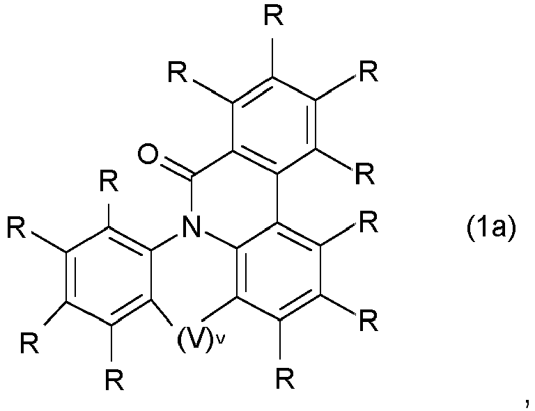
 V est une liaison, C(R0)2, O ou S ;v est 0 ou 1 ;X2 est pour chaque occurrence, de manière identique ou différente, CR1 ou N ;Z est C(R0)2, NR1, O ou S ;n est 0 ou 1 ;Ar1 et Ar2 sont dans chaque cas, de manière indépendante l'un de l'autre, un système de cycle aromatique qui comporte de 6 à 40 atomes de cycle aromatique ou un système de cycle hétéroaromatique qui comporte de 10 à 40 atomes de cycle aromatique, lequel peut être substitué par un radical ou par plusieurs radicaux R3, où le système de cycle hétéroaromatique, qui peut être substitué par un ou plusieurs R3, contient au total seulement un atome de N ou contient au total un ou plusieurs atome(s) de O et/ou de S ;R0 est pour chaque occurrence, de manière identique ou différente, un groupe alkyle en chaîne droite ou ramifié qui comporte de 1 à 4 atome(s) de C ou les deux R0 forment un système de cycle aliphatique, aromatique ou hétéroaromatique monocyclique ou polycyclique, lequel peut être substitué par un radical ou par plusieurs radicaux R2 ;R est sélectionné pour chaque occurrence, de manière identique ou différente, parmi le groupe qui est constitué par H, D, F, Cl, Br, I, CN, NO2,N(Ar)2, N(R2)2, C(=O)Ar, C(=O)R2, P(=O)(Ar)2, P(Ar)2, B(Ar)2, Si(Ar)3, Si(R2)3, un groupe alkyle, alcoxy ou thioalkyle en chaîne droite qui comporte de 1 à 20 atome(s) de C ou un groupe alkyle, alcoxy ou thioalkyle ramifié ou cyclique qui comporte de 3 à 20 atomes de C ou un groupe alkényle qui comporte de 2 à 20 atomes de C, lequel peut dans chaque cas être substitué par un radical ou par plusieurs radicaux R2, où un ou plusieurs groupe(s) CH2 non adjacents peut/peuvent être remplacé(s) par R2C=CR2, Si(R2)2, C=O, C=S, C=NR2, P(=O)(R2), SO, SO2, NR2, O, S ou CONR2 et où un ou plusieurs atome(s) de H peut/peuvent être remplacé(s) par D, F, Cl, Br, I, CN ou NO2,un système de cycle aromatique ou hétéroaromatique qui comporte de 5 à 40 atomes de cycle aromatique, lequel peut dans chaque cas être substitué par un radical ou par plusieurs radicaux R2, un groupe aryloxy ou hétéroaryloxy qui comporte de 5 à 40 atomes de cycle aromatique, lequel peut être substitué par un radical ou par plusieurs radicaux R2, ou un groupe aralkyle ou hétéroaralkyle qui comporte de 5 à 40 atomes de cycle aromatique, lequel peut être substitué par un radical ou par plusieurs radicaux R2 ; deux substituants R qui sont liés au même atome de carbone ou à des atomes de carbone adjacents peuvent en option former un système de cycle aliphatique, aromatique ou hétéroaromatique monocyclique ou polycyclique, lequel peut être substitué par un radical ou par plusieurs radicaux R2 ;R1 est sélectionné pour chaque occurrence, de manière identique ou différente, parmi le groupe qui est constitué par H, D, F, Cl, Br, I, CN, NO2,N(Ar)2, N(R2)2, C(=O)Ar, C(=O)R2, P(=O)(Ar)2, P(Ar)2, B(Ar)2, Si(Ar)3, Si(R2)3, un groupe alkyle, alcoxy ou thioalkyle en chaîne droite qui comporte de 1 à 20 atome(s) de C ou un groupe alkyle, alcoxy ou thioalkyle ramifié ou cyclique qui comporte de 3 à 20 atomes de C ou un groupe alkényle qui comporte de 2 à 20 atomes de C, lequel peut dans chaque cas être substitué par un radical ou par plusieurs radicaux R2, où un ou plusieurs groupe(s) CH2 non adjacents peut/peuvent être remplacé(s) par R2C=CR2, Si(R2)2, C=O, C=S, C=NR2, P(=O)(R2), SO, SO2, NR2, O, S ou CONR2 et où un ou plusieurs atome(s) de H peut/peuvent être remplacé(s) par D, F, Cl, Br, I, CN ou NO2,un système de cycle aromatique ou hétéroaromatique qui comporte de 5 à 40 atomes de cycle aromatique, lequel peut dans chaque cas être substitué par un radical ou par plusieurs radicaux R2, un groupe aryloxy ou hétéroaryloxy qui comporte de 5 à 40 atomes de cycle aromatique, lequel peut être substitué par un radical ou par plusieurs radicaux R2, ou un groupe aralkyle ou hétéroaralkyle qui comporte de 5 à 40 atomes de cycle aromatique, lequel peut être substitué par un radical ou par plusieurs radicaux R2 ,R2 est sélectionné pour chaque occurrence, de manière identique ou différente, parmi le groupe qui est constitué par H, D, F, Cl, Br, I, CN, NO2,N(Ar)2, NH2, N(R3)2, C(=O)Ar, C(=O)H, C(=O)R3, P(=O)(Ar)2, un groupe alkyle, alcoxy ou thioalkyle en chaîne droite qui comporte de 1 à 40 atome(s) de C ou un groupe alkyle, alcoxy ou thioalkyle ramifié ou cyclique qui comporte de 3 à 40 atomes de C ou un groupe alkényle ou alkynyle qui comporte de 2 à 40 atomes de C, lequel peut dans chaque cas être substitué par un radical ou par plusieurs radicaux R3, où un ou plusieurs groupe(s) CH2 non adjacents peut/peuvent être remplacé(s) par HC=CH, R3C=CR3, C=C, Si(R3)2, Ge(R3)2, Sn(R3)2, C=O, C=S, C=Se, C=NR3, P(=O)(R3), SO, SO2, NH, NR3, O, S, CONH ou CONR3 et où un ou plusieurs atome(s) de H peut/peuvent être remplacé(s) par D, F, Cl, Br, I, CN ou NO2,un système de cycle aromatique ou hétéroaromatique qui comporte de 5 à 60 atomes de cycle aromatique, lequel peut dans chaque cas être substitué par un radical ou par plusieurs radicaux R3, un groupe aryloxy ou hétéroaryloxy qui comporte de 5 à 60 atomes de cycle aromatique, lequel peut être substitué par un radical ou par plusieurs radicaux R3, ou une combinaison de ces systèmes, où deux substituants R2 adjacents ou plus peuvent en option former un système de cycle aliphatique, aromatique ou hétéroaromatique monocyclique ou polycyclique, lequel peut être substitué par un radical ou par plusieurs radicaux R3 ;R3 est sélectionné pour chaque occurrence, de manière identique ou différente, parmi le groupe qui est constitué par H, D, F, CN, un radical hydrocarbone aliphatique qui comporte de 1 à 20 atome(s) de C ou un système de cycle aromatique qui comporte de 6 à 30 atomes de cycle ou un système de cycle hétéroaromatique qui comporte de 10 à 30 atomes de cycle, où un ou plusieurs atome(s) de H peut/peuvent être remplacé(s) par D, F, Cl, Br, I ou CN et lequel peut être substitué par un ou plusieurs groupe(s) alkyle, chacun comportant de 1 à 4 atome(s) de carbone ; deux substituants R3 adjacents ou plus peuvent former un système de cycle aliphatique, monoou polycyclique l'un avec l'autre ou les uns avec les autres ;Ar est pour chaque occurrence, de manière identique ou différente, un système de cycle aromatique ou hétéroaromatique qui comporte de 5 à 30 atomes de cycle aromatique, lequel peut être substitué par un radical ou par plusieurs radicaux non aromatique(s) R3 ; deux radicaux Ar qui sont liés au même atome de N, au même atome de P ou au même atome de B peuvent également être pontés l'un à l'autre par une liaison simple ou par un pont qui est sélectionné parmi N(R3), C(R3)2, O ou S.
 - Composition selon la revendication 1, caractérisée en ce que le composé de la formule (1a) correspond à la formule (1b), à la formule (1c), à la formule (1d) ou à la formule (1e),

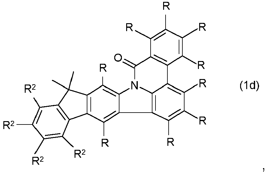

- Composition selon la revendication 1 ou 2, caractérisée en ce que le composé de la formule (2) correspond à la formule (2a),

- Composition selon une ou plusieurs des revendications 1 à 3, caractérisée en ce que l'un des substituants Ar1 et Ar2 représente un système de cycle aromatique qui comporte de 6 à 40 atomes de cycle aromatique ou un système de cycle hétéroaromatique qui comporte de 10 à 40 atomes de cycle aromatique, lequel peut être substitué par un radical ou par plusieurs radicaux R3, où le système de cycle hétéroaromatique, qui peut être substitué par un ou par plusieurs R3, contient au total seulement un atome de N ou contient au total un ou plusieurs atome(s) de O et/ou de S, et l'autre substituant représente un système de cycle aromatique qui comporte de 6 à 40 atomes de cycle aromatique, lequel peut être substitué par un radical ou par plusieurs radicaux R3.
- Composition selon une ou plusieurs des revendications 1 à 4, caractérisée en ce que les substituants Ar1 et Ar2 représentent dans chaque cas, de manière indépendante l'un de l'autre, un système de cycle aromatique qui comporte de 6 à 40 atomes de cycle aromatique, lequel peut être substitué par un radical ou par plusieurs radicaux R3.
- Composition selon une ou plusieurs des revendications 1 à 5, caractérisée en ce que la composition comprend au moins un autre composé qui est sélectionné parmi le groupe qui est constitué par des matériaux d'injection de trous, des matériaux de transport de trous, des matériaux de blocage de trous, des matériaux à bande interdite large, des émetteurs fluorescents, des émetteurs phosphorescents, des matériaux hôtes, des matériaux de blocage d'électrons, des matériaux de transport d'électrons et des matériaux d'injection d'électrons, des dopants de type n et des dopants de type p.
- Formulation comprenant une composition selon une ou plusieurs des revendications 1 à 6 et au moins un solvant.
- Utilisation d'une composition selon une ou plusieurs des revendications 1 à 6 dans un dispositif électronique organique.
- Utilisation selon la revendication 8, caractérisée en ce que le dispositif électronique organique est sélectionné parmi le groupe qui est constitué par les circuits intégrés organiques (OIC), les transistors à effet de champ organiques (OFET), les transistors à film mince organiques (OTFT), les dispositifs électroluminescents organiques, les cellules solaires organiques (OSC), les détecteurs optiques organiques et les photorécepteurs organiques.
- Dispositif électronique organique contenant au moins une composition selon une ou plusieurs des revendications 1 à 6.
- Dispositif selon la revendication 10, caractérisé en ce qu'il est sélectionné parmi le groupe qui est constitué par les circuits intégrés organiques (OIC), les transistors à effet de champ organiques (OFET), les transistors à film mince organiques (OTFT), les dispositifs électroluminescents organiques, les cellules solaires organiques (OSC), les détecteurs optiques organiques et les photorécepteurs organiques.
- Dispositif selon la revendication 10 ou 11, caractérisé en ce qu'il s'agit d'un dispositif électroluminescent qui est sélectionné parmi les transistors à émission de lumière ou électroluminescents organiques (OLET), les dispositifs à extinction de champ organiques (OFQD), les cellules électrochimiques à émission de lumière ou électroluminescentes organiques (OLEC, LEC, LEEC), les diodes laser organiques (O-laser) et les diodes à émission de lumière ou électroluminescentes organiques (OLED).
- Dispositif selon une ou plusieurs des revendications 10 à 12, caractérisé en ce qu'il contient la composition selon une ou plusieurs des revendications 1 à 6 dans une couche d'émission (EML), dans une couche de transport d'électrons (ETL), dans une couche d'injection d'électrons (EIL) et/ou dans une couche de blocage de trous (HBL).
- Dispositif selon une ou plusieurs des revendications 10 à 13, caractérisé en ce qu'il contient la composition selon une ou plusieurs des revendications 1 à 6 dans la couche d'émission en association avec un émetteur phosphorescent.
- Procédé pour la fabrication d'un dispositif selon une ou plusieurs des revendications 10 à 14, caractérisé en ce qu'au moins une couche organique qui comprend une composition selon une ou plusieurs des revendications 1 à 6 est appliquée au moyen d'un dépôt en phase gazeuse ou à partir d'une solution.
- Procédé selon la revendication 15, caractérisé en ce que l'au moins un composé de la formule (1a) et l'au moins un composé de la formule (2), comme il a été décrit selon l'une des revendications 1 à 6, sont déposés à partir de la phase gazeuse en succession ou de façon simultanée à partir d'au moins deux sources de matériau, en option avec d'autres matériaux, et forment la couche organique.
- Procédé selon la revendication 15, caractérisé en ce que la composition selon l'une des revendications 1 à 6 est utilisée en tant que source de matériau pour le dépôt en phase gazeuse et forme la couche organique.
- Procédé selon la revendication 15, caractérisé en ce que la formulation selon la revendication 7 est utilisée afin d'appliquer la couche organique.
Applications Claiming Priority (2)
| Application Number | Priority Date | Filing Date | Title |
|---|---|---|---|
| EP17179785 | 2017-07-05 | ||
| PCT/EP2018/067734 WO2019007867A1 (fr) | 2017-07-05 | 2018-07-02 | Composition pour dispositifs électroniques organiques |
Publications (2)
| Publication Number | Publication Date |
|---|---|
| EP3649213A1 EP3649213A1 (fr) | 2020-05-13 |
| EP3649213B1 true EP3649213B1 (fr) | 2021-06-23 |
Family
ID=59383401
Family Applications (1)
| Application Number | Title | Priority Date | Filing Date |
|---|---|---|---|
| EP18734241.5A Active EP3649213B1 (fr) | 2017-07-05 | 2018-07-02 | Composition pour dispositifs électroniques organiques |
Country Status (7)
| Country | Link |
|---|---|
| US (1) | US11993572B2 (fr) |
| EP (1) | EP3649213B1 (fr) |
| JP (1) | JP7247121B2 (fr) |
| KR (1) | KR102653984B1 (fr) |
| CN (1) | CN110832053B (fr) |
| TW (1) | TWI768075B (fr) |
| WO (1) | WO2019007867A1 (fr) |
Families Citing this family (16)
| Publication number | Priority date | Publication date | Assignee | Title |
|---|---|---|---|---|
| KR102701149B1 (ko) * | 2018-09-07 | 2024-09-03 | 삼성디스플레이 주식회사 | 유기 전계 발광 소자 및 유기 전계 발광 소자용 축합 다환 화합물 |
| KR102173481B1 (ko) * | 2019-04-23 | 2020-11-03 | (주)알로스 | 신규한 유기 발광 화합물 및 이를 포함하는 유기 발광 소자 |
| US20220384735A1 (en) * | 2019-09-20 | 2022-12-01 | Merck Patent Gmbh | Peri-condensed heterocyclic compounds as materials for electronic devices |
| EP4169082A1 (fr) | 2020-06-23 | 2023-04-26 | Merck Patent GmbH | Procédé de production d'un mélange |
| US20240215277A1 (en) | 2021-03-30 | 2024-06-27 | Merck Patent Gmbh | Organic electroluminescent device |
| CN118056484A (zh) | 2021-09-30 | 2024-05-17 | 默克专利有限公司 | 有机电致发光器件 |
| WO2023052376A1 (fr) | 2021-09-30 | 2023-04-06 | Merck Patent Gmbh | Appareil électroluminescent organique |
| WO2023061998A1 (fr) | 2021-10-14 | 2023-04-20 | Merck Patent Gmbh | Matériaux pour dispositifs électroluminescents organiques |
| EP4426701A1 (fr) | 2021-11-02 | 2024-09-11 | Merck Patent GmbH | Dérivés de benzofuro[3,2-d]pyrimidino-2,4-dicarbonitrile et composés similaires pour dispositifs électroluminescents organiques |
| KR20240112926A (ko) | 2021-12-02 | 2024-07-19 | 메르크 파텐트 게엠베하 | 유기 전계발광성 디바이스용 트리페닐렌-트리아진-디벤조푸란/디벤조티오펜 유도체 |
| WO2024038029A1 (fr) | 2022-08-17 | 2024-02-22 | Merck Patent Gmbh | Matériaux pour dispositifs électroluminescents organiques |
| WO2024038068A1 (fr) | 2022-08-19 | 2024-02-22 | Merck Patent Gmbh | Matériaux pour dispositifs électroluminescents organiques |
| WO2024104934A1 (fr) | 2022-11-16 | 2024-05-23 | Merck Patent Gmbh | Matériaux pour dispositifs électroluminescents organiques |
| WO2024121133A1 (fr) | 2022-12-08 | 2024-06-13 | Merck Patent Gmbh | Dispositif électronique organique et matériaux spéciaux pour dispositifs électroniques organiques |
| WO2024133211A1 (fr) | 2022-12-21 | 2024-06-27 | Merck Patent Gmbh | Nouveaux matériaux pour dispositifs électroluminescents organiques |
| WO2024170609A1 (fr) | 2023-02-17 | 2024-08-22 | Merck Patent Gmbh | Matériaux pour dispositifs électroluminescents organiques |
Family Cites Families (148)
| Publication number | Priority date | Publication date | Assignee | Title |
|---|---|---|---|---|
| US4539507A (en) | 1983-03-25 | 1985-09-03 | Eastman Kodak Company | Organic electroluminescent devices having improved power conversion efficiencies |
| US5061569A (en) | 1990-07-26 | 1991-10-29 | Eastman Kodak Company | Electroluminescent device with organic electroluminescent medium |
| US5151629A (en) | 1991-08-01 | 1992-09-29 | Eastman Kodak Company | Blue emitting internal junction organic electroluminescent device (I) |
| DE69432054T2 (de) | 1993-09-29 | 2003-10-09 | Idemitsu Kosan Co | Organische elektrolumineszenzelemente und arylendiaminderivate |
| JPH07133483A (ja) | 1993-11-09 | 1995-05-23 | Shinko Electric Ind Co Ltd | El素子用有機発光材料及びel素子 |
| JPH07244392A (ja) | 1994-03-04 | 1995-09-19 | Canon Inc | 電子写真感光体及び該電子写真感光体を備えた電子写真装置 |
| EP0676461B1 (fr) | 1994-04-07 | 2002-08-14 | Covion Organic Semiconductors GmbH | Composés spiro et leur application comme matières électroluminescentes |
| DE19652261A1 (de) | 1996-12-16 | 1998-06-18 | Hoechst Ag | Arylsubstituierte Poly(p-arylenvinylene), Verfahren zur Herstellung und deren Verwendung in Elektroluminszenzbauelementen |
| US5942340A (en) | 1997-10-02 | 1999-08-24 | Xerox Corporation | Indolocarbazole electroluminescent devices |
| US5843607A (en) | 1997-10-02 | 1998-12-01 | Xerox Corporation | Indolocarbazole photoconductors |
| US5952115A (en) | 1997-10-02 | 1999-09-14 | Xerox Corporation | Electroluminescent devices |
| JP3302945B2 (ja) | 1998-06-23 | 2002-07-15 | ネースディスプレイ・カンパニー・リミテッド | 新規な有機金属発光物質およびそれを含む有機電気発光素子 |
| JP3992929B2 (ja) | 1999-05-13 | 2007-10-17 | ザ、トラスティーズ オブ プリンストン ユニバーシティ | 電気リン光に基づく高効率有機発光装置 |
| JP4357781B2 (ja) | 1999-12-01 | 2009-11-04 | ザ、トラスティーズ オブ プリンストン ユニバーシティ | 有機led用燐光性ドーパントとしての式l2mxの錯体 |
| KR100377321B1 (ko) | 1999-12-31 | 2003-03-26 | 주식회사 엘지화학 | 피-형 반도체 성질을 갖는 유기 화합물을 포함하는 전기소자 |
| US6660410B2 (en) | 2000-03-27 | 2003-12-09 | Idemitsu Kosan Co., Ltd. | Organic electroluminescence element |
| US6392250B1 (en) | 2000-06-30 | 2002-05-21 | Xerox Corporation | Organic light emitting devices having improved performance |
| US20020121638A1 (en) | 2000-06-30 | 2002-09-05 | Vladimir Grushin | Electroluminescent iridium compounds with fluorinated phenylpyridines, phenylpyrimidines, and phenylquinolines and devices made with such compounds |
| EP1325671B1 (fr) | 2000-08-11 | 2012-10-24 | The Trustees Of Princeton University | Composes organometalliques et electrophosphorescence organique presentant un deplacement d'emission |
| JP4154138B2 (ja) | 2000-09-26 | 2008-09-24 | キヤノン株式会社 | 発光素子、表示装置及び金属配位化合物 |
| JP4154139B2 (ja) | 2000-09-26 | 2008-09-24 | キヤノン株式会社 | 発光素子 |
| JP4154140B2 (ja) | 2000-09-26 | 2008-09-24 | キヤノン株式会社 | 金属配位化合物 |
| US6803720B2 (en) | 2000-12-15 | 2004-10-12 | Universal Display Corporation | Highly stable and efficient OLEDs with a phosphorescent-doped mixed layer architecture |
| AU2002306698A1 (en) | 2001-03-14 | 2002-09-24 | The Trustees Of Princeton University | Materials and devices for blue phosphorescence based organic light emitting diodes |
| KR100691543B1 (ko) | 2002-01-18 | 2007-03-09 | 주식회사 엘지화학 | 새로운 전자 수송용 물질 및 이를 이용한 유기 발광 소자 |
| CN100449818C (zh) | 2002-09-20 | 2009-01-07 | 出光兴产株式会社 | 有机电致发光元件 |
| WO2004058911A2 (fr) | 2002-12-23 | 2004-07-15 | Covion Organic Semiconductors Gmbh | Element electroluminescent organique |
| DE10310887A1 (de) | 2003-03-11 | 2004-09-30 | Covion Organic Semiconductors Gmbh | Matallkomplexe |
| EP2174932B1 (fr) | 2003-03-13 | 2019-07-03 | Idemitsu Kosan Co., Ltd. | Dérivé hétérocyclique contenant de l'azote et élément électroluminescent organique utilisant ce dérivé |
| JP4411851B2 (ja) | 2003-03-19 | 2010-02-10 | コニカミノルタホールディングス株式会社 | 有機エレクトロルミネッセンス素子 |
| KR101162933B1 (ko) | 2003-04-15 | 2012-07-05 | 메르크 파텐트 게엠베하 | 매트릭스 재료 및 방출 가능 유기 반도체의 혼합물, 그의 용도 및 상기 혼합물을 함유하는 전자 부품 |
| WO2004095889A1 (fr) | 2003-04-23 | 2004-11-04 | Konica Minolta Holdings, Inc. | Dispositif organique electroluminescent et affichage |
| EP1644459B1 (fr) | 2003-07-07 | 2017-08-23 | Merck Patent GmbH | Melanges de semi-conducteurs organiques aptes a l'emission et de materiaux matriciels, et composants electroniques contenant ces melanges |
| DE10333232A1 (de) | 2003-07-21 | 2007-10-11 | Merck Patent Gmbh | Organisches Elektrolumineszenzelement |
| DE10338550A1 (de) | 2003-08-19 | 2005-03-31 | Basf Ag | Übergangsmetallkomplexe mit Carbenliganden als Emitter für organische Licht-emittierende Dioden (OLEDs) |
| DE10345572A1 (de) | 2003-09-29 | 2005-05-19 | Covion Organic Semiconductors Gmbh | Metallkomplexe |
| US7795801B2 (en) | 2003-09-30 | 2010-09-14 | Konica Minolta Holdings, Inc. | Organic electroluminescent element, illuminator, display and compound |
| DE10357044A1 (de) | 2003-12-04 | 2005-07-14 | Novaled Gmbh | Verfahren zur Dotierung von organischen Halbleitern mit Chinondiiminderivaten |
| DE102004008304A1 (de) | 2004-02-20 | 2005-09-08 | Covion Organic Semiconductors Gmbh | Organische elektronische Vorrichtungen |
| DE102004010954A1 (de) | 2004-03-03 | 2005-10-06 | Novaled Gmbh | Verwendung eines Metallkomplexes als n-Dotand für ein organisches halbleitendes Matrixmaterial, organisches Halbleitermaterial und elektronisches Bauteil |
| US7790890B2 (en) | 2004-03-31 | 2010-09-07 | Konica Minolta Holdings, Inc. | Organic electroluminescence element material, organic electroluminescence element, display device and illumination device |
| KR100787425B1 (ko) | 2004-11-29 | 2007-12-26 | 삼성에스디아이 주식회사 | 페닐카바졸계 화합물 및 이를 이용한 유기 전계 발광 소자 |
| DE102004023277A1 (de) | 2004-05-11 | 2005-12-01 | Covion Organic Semiconductors Gmbh | Neue Materialmischungen für die Elektrolumineszenz |
| US7598388B2 (en) | 2004-05-18 | 2009-10-06 | The University Of Southern California | Carbene containing metal complexes as OLEDs |
| JP4862248B2 (ja) | 2004-06-04 | 2012-01-25 | コニカミノルタホールディングス株式会社 | 有機エレクトロルミネッセンス素子、照明装置及び表示装置 |
| EP1655359A1 (fr) | 2004-11-06 | 2006-05-10 | Covion Organic Semiconductors GmbH | Dispositif organique électroluminescent |
| WO2006081780A1 (fr) | 2005-02-04 | 2006-08-10 | Novaled Ag | Dopants pour semi-conducteurs organiques |
| KR100949214B1 (ko) | 2005-03-18 | 2010-03-24 | 이데미쓰 고산 가부시키가이샤 | 방향족 아민 유도체 및 그것을 사용한 유기 전기발광 소자 |
| CN101155895B (zh) | 2005-04-14 | 2011-12-28 | 默克专利有限公司 | 用于有机电子器件的化合物 |
| WO2006117052A1 (fr) | 2005-05-03 | 2006-11-09 | Merck Patent Gmbh | Dispositif electroluminescent organique, et derives d'acide boronique et d'acide borinique utilises pour produire ce dispositif electroluminescent organique |
| DE102005023437A1 (de) | 2005-05-20 | 2006-11-30 | Merck Patent Gmbh | Verbindungen für organische elektronische Vorrichtungen |
| US7993760B2 (en) | 2005-12-01 | 2011-08-09 | Nippon Steel Chemical Co., Ltd. | Compound for use in organic electroluminescent device and organic electroluminescent device |
| US7919010B2 (en) | 2005-12-22 | 2011-04-05 | Novaled Ag | Doped organic semiconductor material |
| EP1837927A1 (fr) | 2006-03-22 | 2007-09-26 | Novaled AG | Utilisation de radicaux hétérocycliques pour doper des semiconducteurs organiques |
| EP1837926B1 (fr) | 2006-03-21 | 2008-05-07 | Novaled AG | Radicaux ou diradicaux hétérocycliques, leur dimères, oligomères, polymères, composés spiro et polycycliques. Leur usage dans des semi-conducteurs organiques et dispositifs électroniques. |
| DE112007000789B4 (de) | 2006-03-30 | 2012-03-15 | Novaled Ag | Verwendung von Bora-tetraazepentalenen |
| EP1860709B1 (fr) | 2006-05-24 | 2012-08-08 | Novaled AG | Utilisation des complexes plans quadrangulaires à base des métaux de transition comme dopant |
| DE102006025777A1 (de) | 2006-05-31 | 2007-12-06 | Merck Patent Gmbh | Neue Materialien für organische Elektrolumineszenzvorrichtungen |
| DE102006025846A1 (de) | 2006-06-02 | 2007-12-06 | Merck Patent Gmbh | Neue Materialien für organische Elektrolumineszenzvorrichtungen |
| DE102006031990A1 (de) | 2006-07-11 | 2008-01-17 | Merck Patent Gmbh | Neue Materialien für organische Elektrolumineszenzvorrichtungen |
| KR100955993B1 (ko) | 2006-11-09 | 2010-05-04 | 신닛테츠가가쿠 가부시키가이샤 | 유기 전계 발광 소자용 화합물 및 유기 전계 발광 소자 |
| DE102006053320B4 (de) | 2006-11-13 | 2012-01-19 | Novaled Ag | Verwendung einer Koordinationsverbindung zur Dotierung organischer Halbleiter |
| DE102006054524B4 (de) | 2006-11-20 | 2022-12-22 | Novaled Gmbh | Verwendung von Dithiolenübergangsmetallkomplexen und Selen- analoger Verbindungen als Dotand |
| DE102006054523B4 (de) | 2006-11-20 | 2009-07-23 | Novaled Ag | Dithiolenübergangsmetallkomplexe und Selen-analoge Verbindungen, deren Verwendung als Dotand, organisches halbleitendes Material enthaltend die Komplexe, sowie elektronische oder optoelektronisches Bauelement enthaltend einen Komplex |
| DE102007002714A1 (de) | 2007-01-18 | 2008-07-31 | Merck Patent Gmbh | Neue Materialien für organische Elektrolumineszenzvorrichtungen |
| DE102007018456B4 (de) | 2007-04-19 | 2022-02-24 | Novaled Gmbh | Verwendung von Hauptgruppenelementhalogeniden und/oder -pseudohalogeniden, organisches halbleitendes Matrixmaterial, elektronische und optoelektronische Bauelemente |
| EP3457451B1 (fr) | 2007-04-30 | 2019-07-17 | Novaled GmbH | L'utilisation de composé d'oxydes de carbone, de composé de pseudo oxyde de carbone et de composé de radialène |
| EP1990847B1 (fr) | 2007-05-10 | 2018-06-20 | Novaled GmbH | Utilisation de bisimidazoles quinoïdes et leurs dérivés en tant que dopant destiné au dopage d'un matériau de matrice organique semi-conducteur |
| DE102007024850A1 (de) | 2007-05-29 | 2008-12-04 | Merck Patent Gmbh | Neue Materialien für organische Elektrolumineszenzvorrichtungen |
| EP2009014B1 (fr) | 2007-06-22 | 2018-10-24 | Novaled GmbH | Utilisation d'un précurseur d'un n-dopant destiné au dopage d'un matériau semi-conducteur organique, précurseur et composant électronique ou optoélectronique |
| DE102007031220B4 (de) | 2007-07-04 | 2022-04-28 | Novaled Gmbh | Chinoide Verbindungen und deren Verwendung in halbleitenden Matrixmaterialien, elektronischen und optoelektronischen Bauelementen |
| DE102008051737B4 (de) | 2007-10-24 | 2022-10-06 | Novaled Gmbh | Quadratisch planare Übergangsmetallkomplexe, organische halbleitende Materialien sowie elektronische oder optoelektronische Bauelemente, die diese umfassen und Verwendung derselben |
| DE102007053771A1 (de) | 2007-11-12 | 2009-05-14 | Merck Patent Gmbh | Organische Elektrolumineszenzvorrichtungen |
| WO2009069442A1 (fr) | 2007-11-26 | 2009-06-04 | Konica Minolta Holdings, Inc. | Dispositif électroluminescent organique, dispositif d'affichage et dispositif d'éclairage |
| DE112009000621A5 (de) | 2008-01-15 | 2010-12-16 | Novaled Ag | Dithiolenübergangsmetallkomplexe und elektronische oder optoelektronische Bauelemente |
| US8057712B2 (en) | 2008-04-29 | 2011-11-15 | Novaled Ag | Radialene compounds and their use |
| DE102008027005A1 (de) | 2008-06-05 | 2009-12-10 | Merck Patent Gmbh | Organische elektronische Vorrichtung enthaltend Metallkomplexe |
| DE102008033943A1 (de) | 2008-07-18 | 2010-01-21 | Merck Patent Gmbh | Neue Materialien für organische Elektrolumineszenzvorrichtungen |
| DE102008035413A1 (de) | 2008-07-29 | 2010-02-04 | Merck Patent Gmbh | Verbindungen für organische elektronische Vorrichtungen |
| DE102008036247A1 (de) | 2008-08-04 | 2010-02-11 | Merck Patent Gmbh | Elektronische Vorrichtungen enthaltend Metallkomplexe |
| DE102008036982A1 (de) | 2008-08-08 | 2010-02-11 | Merck Patent Gmbh | Organische Elektrolumineszenzvorrichtung |
| DE102008048336A1 (de) | 2008-09-22 | 2010-03-25 | Merck Patent Gmbh | Einkernige neutrale Kupfer(I)-Komplexe und deren Verwendung zur Herstellung von optoelektronischen Bauelementen |
| US8119037B2 (en) | 2008-10-16 | 2012-02-21 | Novaled Ag | Square planar transition metal complexes and organic semiconductive materials using them as well as electronic or optoelectric components |
| EP2180029B1 (fr) | 2008-10-23 | 2011-07-27 | Novaled AG | Composés de Radialène et leur utilisation |
| DE102008056688A1 (de) | 2008-11-11 | 2010-05-12 | Merck Patent Gmbh | Materialien für organische Elektrolumineszenzvorrichtungen |
| WO2010054730A1 (fr) | 2008-11-11 | 2010-05-20 | Merck Patent Gmbh | Dispositifs électroluminescents organiques |
| DE102008057051B4 (de) | 2008-11-13 | 2021-06-17 | Merck Patent Gmbh | Materialien für organische Elektrolumineszenzvorrichtungen |
| DE102008057050B4 (de) | 2008-11-13 | 2021-06-02 | Merck Patent Gmbh | Materialien für organische Elektrolumineszenzvorrichtungen |
| DE102008064200A1 (de) | 2008-12-22 | 2010-07-01 | Merck Patent Gmbh | Organische Elektrolumineszenzvorrichtung |
| DE102009007038A1 (de) | 2009-02-02 | 2010-08-05 | Merck Patent Gmbh | Metallkomplexe |
| EP2401254B1 (fr) | 2009-02-26 | 2013-06-19 | Novaled AG | Composés quinoniques convenant comme impureté de dopage en électronique organique |
| DE102009011223A1 (de) | 2009-03-02 | 2010-09-23 | Merck Patent Gmbh | Metallkomplexe |
| DE102009013041A1 (de) | 2009-03-13 | 2010-09-16 | Merck Patent Gmbh | Materialien für organische Elektrolumineszenzvorrichtungen |
| DE102009014513A1 (de) | 2009-03-23 | 2010-09-30 | Merck Patent Gmbh | Organische Elektrolumineszenzvorrichtung |
| DE102009023155A1 (de) | 2009-05-29 | 2010-12-02 | Merck Patent Gmbh | Materialien für organische Elektrolumineszenzvorrichtungen |
| DE102009031021A1 (de) | 2009-06-30 | 2011-01-05 | Merck Patent Gmbh | Materialien für organische Elektrolumineszenzvorrichtungen |
| DE102009041414A1 (de) | 2009-09-16 | 2011-03-17 | Merck Patent Gmbh | Metallkomplexe |
| US9266851B2 (en) | 2009-10-16 | 2016-02-23 | Idemitsu Kosan Co., Ltd. | Fluorene-containing aromatic compound, material for organic electroluminescent element, and organic electroluminescent element using same |
| DE102009053382A1 (de) | 2009-11-14 | 2011-05-19 | Merck Patent Gmbh | Materialien für elektronische Vorrichtungen |
| DE102009057167A1 (de) | 2009-12-05 | 2011-06-09 | Merck Patent Gmbh | Elektronische Vorrichtung enthaltend Metallkomplexe |
| DE102010005697A1 (de) | 2010-01-25 | 2011-07-28 | Merck Patent GmbH, 64293 | Verbindungen für elektronische Vorrichtungen |
| DE102010014933A1 (de) | 2010-04-14 | 2011-10-20 | Merck Patent Gmbh | Materialien für elektronische Vorrichtungen |
| WO2011131185A1 (fr) | 2010-04-21 | 2011-10-27 | Novaled Ag | Mélange pour la fabrication d'une couche semi-conductrice dopée |
| CN102892859B (zh) | 2010-04-27 | 2016-03-09 | 诺瓦莱德公开股份有限公司 | 有机半导体材料和电子构件 |
| DE102010019306B4 (de) * | 2010-05-04 | 2021-05-20 | Merck Patent Gmbh | Organische Elektrolumineszenzvorrichtungen |
| WO2011157339A1 (fr) | 2010-06-15 | 2011-12-22 | Merck Patent Gmbh | Complexes métalliques |
| DE102010027317A1 (de) | 2010-07-16 | 2012-01-19 | Merck Patent Gmbh | Metallkomplexe |
| DE102010033778A1 (de) | 2010-08-09 | 2012-02-09 | Merck Patent Gmbh | Polymere mit Carbazol-Struktureinheiten |
| WO2012031735A1 (fr) | 2010-09-10 | 2012-03-15 | Novaled Ag | Composés pour dispositifs photovoltaïques organiques |
| DE102010045405A1 (de) | 2010-09-15 | 2012-03-15 | Merck Patent Gmbh | Materialien für organische Elektrolumineszenzvorrichtungen |
| DE102010046040B4 (de) | 2010-09-22 | 2021-11-11 | Novaled Gmbh | Verfahren zur Herstellung von Fulleren-Derivaten |
| EP2452946B1 (fr) | 2010-11-16 | 2014-05-07 | Novaled AG | Oxides de pyridylphosphine pour dispositif électronique organique et dispositif électronique organique |
| EP2463927B1 (fr) | 2010-12-08 | 2013-08-21 | Novaled AG | Matériau pour dispositif électronique organique et dispositif électronique organique |
| TWI526418B (zh) | 2011-03-01 | 2016-03-21 | 諾瓦發光二極體股份公司 | 有機半導體材料及有機組成物 |
| EP2705552B1 (fr) | 2011-05-05 | 2015-03-04 | Merck Patent GmbH | Composés pour dispositifs électroniques |
| JP2014520394A (ja) | 2011-06-09 | 2014-08-21 | ノヴァレッド・アクチエンゲゼルシャフト | 有機電子素子のための化合物 |
| US20140203254A1 (en) | 2011-06-22 | 2014-07-24 | Max-Planck-Gesellschaft Zur Foerderung Der Wissenschaften E.V. | Organic Electronic Component |
| JP6461599B2 (ja) | 2011-06-22 | 2019-01-30 | ノヴァレッド ゲーエムベーハー | 電子装置 |
| CN104024371B (zh) | 2011-11-01 | 2015-11-25 | 默克专利有限公司 | 有机电致发光器件 |
| KR20210124523A (ko) | 2011-11-17 | 2021-10-14 | 메르크 파텐트 게엠베하 | 스피로디히드로아크리딘 유도체 및 이의 유기 전계발광 소자용 재료로서의 용도 |
| DE102012202146A1 (de) * | 2012-02-13 | 2013-08-14 | Bayerische Motoren Werke Aktiengesellschaft | Speicherbehälter von kryogenem Druckgas mit einem Speichervolumen |
| CN104428392B (zh) | 2012-07-13 | 2017-05-31 | 默克专利有限公司 | 金属络合物 |
| KR102337198B1 (ko) | 2012-07-23 | 2021-12-09 | 메르크 파텐트 게엠베하 | 화합물 및 유기 전계 발광 디바이스 |
| CN104507932B (zh) | 2012-07-23 | 2016-12-07 | 默克专利有限公司 | 用于有机电致发光器件的材料 |
| JP6430378B2 (ja) | 2012-07-23 | 2018-11-28 | メルク パテント ゲーエムベーハー | 2−ジアリールアミノフルオレン誘導体およびそれらを含む有機電子素子 |
| EP3424907A3 (fr) | 2012-07-23 | 2019-02-13 | Merck Patent GmbH | Raccordements et dispositifs électro-organiques |
| WO2014023377A2 (fr) | 2012-08-07 | 2014-02-13 | Merck Patent Gmbh | Complexes métalliques |
| CN104871329B (zh) * | 2012-12-18 | 2017-10-24 | 默克专利有限公司 | 有机电致发光器件 |
| WO2014094961A1 (fr) | 2012-12-21 | 2014-06-26 | Merck Patent Gmbh | Complexes métalliques |
| JP6556628B2 (ja) | 2012-12-21 | 2019-08-07 | メルク パテント ゲーエムベーハー | 金属錯体 |
| WO2015000542A1 (fr) | 2013-07-02 | 2015-01-08 | Merck Patent Gmbh | Composés de lactame spirocondensés pour des dispositifs électroluminescents organiques |
| EP3044284B1 (fr) | 2013-09-11 | 2019-11-13 | Merck Patent GmbH | Complexes métalliques |
| WO2015082046A2 (fr) | 2013-12-06 | 2015-06-11 | Merck Patent Gmbh | Oxépines substituées |
| JP6618927B2 (ja) | 2014-01-13 | 2019-12-11 | メルク、パテント、ゲゼルシャフト、ミット、ベシュレンクテル、ハフツングMerck Patent GmbH | 金属錯体 |
| CN105916963B (zh) * | 2014-01-17 | 2019-03-29 | 默克专利有限公司 | 用于有机电致发光器件的材料 |
| KR102349550B1 (ko) | 2014-02-05 | 2022-01-11 | 메르크 파텐트 게엠베하 | 금속 착물 |
| WO2015128052A1 (fr) | 2014-02-28 | 2015-09-03 | Merck Patent Gmbh | Matières pour dispositifs électroluminescents organiques |
| CN106459018B (zh) | 2014-05-05 | 2022-01-25 | 默克专利有限公司 | 用于有机发光器件的材料 |
| DE102014008722B4 (de) * | 2014-06-18 | 2024-08-22 | Merck Patent Gmbh | Zusammensetzungen für elektronische Vorrichtungen, Formulierung diese enthaltend, Verwendung der Zusammensetzung, Verwendung der Formulierung sowie organische elektronische Vorrichtung enthaltend die Zusammensetzung |
| WO2016013875A1 (fr) * | 2014-07-22 | 2016-01-28 | Rohm And Haas Electronic Materials Korea Ltd. | Dispositif électroluminescent organique |
| KR102357467B1 (ko) * | 2014-07-22 | 2022-02-04 | 롬엔드하스전자재료코리아유한회사 | 유기 전계 발광 소자 |
| EP3174890B1 (fr) | 2014-07-28 | 2019-03-13 | Merck Patent GmbH | Complexes métalliques |
| WO2016028110A1 (fr) * | 2014-08-20 | 2016-02-25 | Rohm And Haas Electronic Materials Korea Ltd. | Pluralité de matériaux hôtes et dispositif électroluminescent organique comprenant ces matériaux |
| WO2016062376A1 (fr) * | 2014-10-24 | 2016-04-28 | Merck Patent Gmbh | Dispositif électroluminescent organique |
| EP3254317B1 (fr) | 2015-02-03 | 2019-07-31 | Merck Patent GmbH | Complexes métalliques |
| EP3341385B1 (fr) | 2015-08-25 | 2020-03-11 | Merck Patent GmbH | Complexes métalliques |
| WO2018178001A1 (fr) * | 2017-03-29 | 2018-10-04 | Merck Patent Gmbh | Complexes métalliques |
| KR20200120698A (ko) * | 2018-02-13 | 2020-10-21 | 메르크 파텐트 게엠베하 | 금속 착물 |
-
2018
- 2018-07-02 WO PCT/EP2018/067734 patent/WO2019007867A1/fr unknown
- 2018-07-02 US US16/628,297 patent/US11993572B2/en active Active
- 2018-07-02 EP EP18734241.5A patent/EP3649213B1/fr active Active
- 2018-07-02 TW TW107122747A patent/TWI768075B/zh active
- 2018-07-02 JP JP2019572002A patent/JP7247121B2/ja active Active
- 2018-07-02 KR KR1020207003241A patent/KR102653984B1/ko active IP Right Grant
- 2018-07-02 CN CN201880043357.4A patent/CN110832053B/zh active Active
Non-Patent Citations (1)
| Title |
|---|
| None * |
Also Published As
| Publication number | Publication date |
|---|---|
| WO2019007867A1 (fr) | 2019-01-10 |
| JP2020526026A (ja) | 2020-08-27 |
| KR102653984B1 (ko) | 2024-04-02 |
| KR20200024907A (ko) | 2020-03-09 |
| US20200216391A1 (en) | 2020-07-09 |
| TW201920101A (zh) | 2019-06-01 |
| CN110832053B (zh) | 2024-06-04 |
| TWI768075B (zh) | 2022-06-21 |
| EP3649213A1 (fr) | 2020-05-13 |
| JP7247121B2 (ja) | 2023-03-28 |
| CN110832053A (zh) | 2020-02-21 |
| US11993572B2 (en) | 2024-05-28 |
Similar Documents
| Publication | Publication Date | Title |
|---|---|---|
| EP3649213B1 (fr) | Composition pour dispositifs électroniques organiques | |
| EP4118696B1 (fr) | Appareil électroluminescent organique | |
| EP2907173B1 (fr) | Dispositif électronique | |
| EP3609977B1 (fr) | Composition pour dispositifs électroniques organiques | |
| EP3649123B1 (fr) | Composition pour dispositifs électroniques organiques | |
| EP2898042B1 (fr) | Matériaux pour dispositifs électroniques | |
| EP4118695B1 (fr) | Appareil électroluminescent organique | |
| EP3210248B2 (fr) | Matériaux pour dispositifs électroniques | |
| WO2019229011A1 (fr) | Composition pour dispositifs électroniques organiques | |
| EP4369378A2 (fr) | Dispositifs électroniques | |
| EP4237506B1 (fr) | Dispositif électroluminescent organique | |
| EP3928360A1 (fr) | Composition pour dispositifs électroniques organiques | |
| EP3710557B1 (fr) | Composition pour dispositifs électroniques organiques | |
| WO2021239772A1 (fr) | Appareil électroluminescent organique | |
| EP2941470B1 (fr) | Dispositif électronique | |
| EP2941473B1 (fr) | Dispositif électronique | |
| EP4055641B1 (fr) | Appareil électroluminescent organique | |
| WO2023247662A1 (fr) | Composition pour dispositifs électroniques organiques | |
| EP4031638A1 (fr) | Mélange de deux matériaux hôtes et dispositif électroluminescent organique l'utilisant | |
| WO2024013004A1 (fr) | Matériaux pour dispositifs électroniques | |
| WO2024013275A1 (fr) | Matériaux pour dispositifs électroniques | |
| WO2024121133A1 (fr) | Dispositif électronique organique et matériaux spéciaux pour dispositifs électroniques organiques | |
| WO2024133211A1 (fr) | Nouveaux matériaux pour dispositifs électroluminescents organiques |
Legal Events
| Date | Code | Title | Description |
|---|---|---|---|
| STAA | Information on the status of an ep patent application or granted ep patent |
Free format text: STATUS: UNKNOWN |
|
| STAA | Information on the status of an ep patent application or granted ep patent |
Free format text: STATUS: THE INTERNATIONAL PUBLICATION HAS BEEN MADE |
|
| PUAI | Public reference made under article 153(3) epc to a published international application that has entered the european phase |
Free format text: ORIGINAL CODE: 0009012 |
|
| STAA | Information on the status of an ep patent application or granted ep patent |
Free format text: STATUS: REQUEST FOR EXAMINATION WAS MADE |
|
| 17P | Request for examination filed |
Effective date: 20191220 |
|
| AK | Designated contracting states |
Kind code of ref document: A1 Designated state(s): AL AT BE BG CH CY CZ DE DK EE ES FI FR GB GR HR HU IE IS IT LI LT LU LV MC MK MT NL NO PL PT RO RS SE SI SK SM TR |
|
| AX | Request for extension of the european patent |
Extension state: BA ME |
|
| DAV | Request for validation of the european patent (deleted) | ||
| DAX | Request for extension of the european patent (deleted) | ||
| STAA | Information on the status of an ep patent application or granted ep patent |
Free format text: STATUS: EXAMINATION IS IN PROGRESS |
|
| STAA | Information on the status of an ep patent application or granted ep patent |
Free format text: STATUS: EXAMINATION IS IN PROGRESS |
|
| 17Q | First examination report despatched |
Effective date: 20201106 |
|
| GRAP | Despatch of communication of intention to grant a patent |
Free format text: ORIGINAL CODE: EPIDOSNIGR1 |
|
| STAA | Information on the status of an ep patent application or granted ep patent |
Free format text: STATUS: GRANT OF PATENT IS INTENDED |
|
| RIC1 | Information provided on ipc code assigned before grant |
Ipc: C09K 11/06 20060101AFI20210304BHEP Ipc: H01L 51/50 20060101ALI20210304BHEP Ipc: H01L 51/00 20060101ALI20210304BHEP |
|
| INTG | Intention to grant announced |
Effective date: 20210322 |
|
| GRAS | Grant fee paid |
Free format text: ORIGINAL CODE: EPIDOSNIGR3 |
|
| GRAA | (expected) grant |
Free format text: ORIGINAL CODE: 0009210 |
|
| STAA | Information on the status of an ep patent application or granted ep patent |
Free format text: STATUS: THE PATENT HAS BEEN GRANTED |
|
| AK | Designated contracting states |
Kind code of ref document: B1 Designated state(s): AL AT BE BG CH CY CZ DE DK EE ES FI FR GB GR HR HU IE IS IT LI LT LU LV MC MK MT NL NO PL PT RO RS SE SI SK SM TR |
|
| REG | Reference to a national code |
Ref country code: GB Ref legal event code: FG4D Free format text: NOT ENGLISH |
|
| REG | Reference to a national code |
Ref country code: CH Ref legal event code: EP |
|
| REG | Reference to a national code |
Ref country code: DE Ref legal event code: R096 Ref document number: 502018005840 Country of ref document: DE Ref country code: AT Ref legal event code: REF Ref document number: 1404319 Country of ref document: AT Kind code of ref document: T Effective date: 20210715 |
|
| REG | Reference to a national code |
Ref country code: IE Ref legal event code: FG4D Free format text: LANGUAGE OF EP DOCUMENT: GERMAN |
|
| REG | Reference to a national code |
Ref country code: LT Ref legal event code: MG9D |
|
| PG25 | Lapsed in a contracting state [announced via postgrant information from national office to epo] |
Ref country code: BG Free format text: LAPSE BECAUSE OF FAILURE TO SUBMIT A TRANSLATION OF THE DESCRIPTION OR TO PAY THE FEE WITHIN THE PRESCRIBED TIME-LIMIT Effective date: 20210923 Ref country code: HR Free format text: LAPSE BECAUSE OF FAILURE TO SUBMIT A TRANSLATION OF THE DESCRIPTION OR TO PAY THE FEE WITHIN THE PRESCRIBED TIME-LIMIT Effective date: 20210623 Ref country code: LT Free format text: LAPSE BECAUSE OF FAILURE TO SUBMIT A TRANSLATION OF THE DESCRIPTION OR TO PAY THE FEE WITHIN THE PRESCRIBED TIME-LIMIT Effective date: 20210623 Ref country code: FI Free format text: LAPSE BECAUSE OF FAILURE TO SUBMIT A TRANSLATION OF THE DESCRIPTION OR TO PAY THE FEE WITHIN THE PRESCRIBED TIME-LIMIT Effective date: 20210623 |
|
| PG25 | Lapsed in a contracting state [announced via postgrant information from national office to epo] |
Ref country code: SE Free format text: LAPSE BECAUSE OF FAILURE TO SUBMIT A TRANSLATION OF THE DESCRIPTION OR TO PAY THE FEE WITHIN THE PRESCRIBED TIME-LIMIT Effective date: 20210623 Ref country code: RS Free format text: LAPSE BECAUSE OF FAILURE TO SUBMIT A TRANSLATION OF THE DESCRIPTION OR TO PAY THE FEE WITHIN THE PRESCRIBED TIME-LIMIT Effective date: 20210623 Ref country code: LV Free format text: LAPSE BECAUSE OF FAILURE TO SUBMIT A TRANSLATION OF THE DESCRIPTION OR TO PAY THE FEE WITHIN THE PRESCRIBED TIME-LIMIT Effective date: 20210623 Ref country code: NO Free format text: LAPSE BECAUSE OF FAILURE TO SUBMIT A TRANSLATION OF THE DESCRIPTION OR TO PAY THE FEE WITHIN THE PRESCRIBED TIME-LIMIT Effective date: 20210923 Ref country code: GR Free format text: LAPSE BECAUSE OF FAILURE TO SUBMIT A TRANSLATION OF THE DESCRIPTION OR TO PAY THE FEE WITHIN THE PRESCRIBED TIME-LIMIT Effective date: 20210924 |
|
| REG | Reference to a national code |
Ref country code: NL Ref legal event code: MP Effective date: 20210623 |
|
| PG25 | Lapsed in a contracting state [announced via postgrant information from national office to epo] |
Ref country code: EE Free format text: LAPSE BECAUSE OF FAILURE TO SUBMIT A TRANSLATION OF THE DESCRIPTION OR TO PAY THE FEE WITHIN THE PRESCRIBED TIME-LIMIT Effective date: 20210623 Ref country code: ES Free format text: LAPSE BECAUSE OF FAILURE TO SUBMIT A TRANSLATION OF THE DESCRIPTION OR TO PAY THE FEE WITHIN THE PRESCRIBED TIME-LIMIT Effective date: 20210623 Ref country code: SK Free format text: LAPSE BECAUSE OF FAILURE TO SUBMIT A TRANSLATION OF THE DESCRIPTION OR TO PAY THE FEE WITHIN THE PRESCRIBED TIME-LIMIT Effective date: 20210623 Ref country code: CZ Free format text: LAPSE BECAUSE OF FAILURE TO SUBMIT A TRANSLATION OF THE DESCRIPTION OR TO PAY THE FEE WITHIN THE PRESCRIBED TIME-LIMIT Effective date: 20210623 Ref country code: SM Free format text: LAPSE BECAUSE OF FAILURE TO SUBMIT A TRANSLATION OF THE DESCRIPTION OR TO PAY THE FEE WITHIN THE PRESCRIBED TIME-LIMIT Effective date: 20210623 Ref country code: RO Free format text: LAPSE BECAUSE OF FAILURE TO SUBMIT A TRANSLATION OF THE DESCRIPTION OR TO PAY THE FEE WITHIN THE PRESCRIBED TIME-LIMIT Effective date: 20210623 Ref country code: NL Free format text: LAPSE BECAUSE OF FAILURE TO SUBMIT A TRANSLATION OF THE DESCRIPTION OR TO PAY THE FEE WITHIN THE PRESCRIBED TIME-LIMIT Effective date: 20210623 Ref country code: PT Free format text: LAPSE BECAUSE OF FAILURE TO SUBMIT A TRANSLATION OF THE DESCRIPTION OR TO PAY THE FEE WITHIN THE PRESCRIBED TIME-LIMIT Effective date: 20211025 |
|
| PG25 | Lapsed in a contracting state [announced via postgrant information from national office to epo] |
Ref country code: PL Free format text: LAPSE BECAUSE OF FAILURE TO SUBMIT A TRANSLATION OF THE DESCRIPTION OR TO PAY THE FEE WITHIN THE PRESCRIBED TIME-LIMIT Effective date: 20210623 |
|
| REG | Reference to a national code |
Ref country code: CH Ref legal event code: PL |
|
| REG | Reference to a national code |
Ref country code: DE Ref legal event code: R097 Ref document number: 502018005840 Country of ref document: DE |
|
| PG25 | Lapsed in a contracting state [announced via postgrant information from national office to epo] |
Ref country code: MC Free format text: LAPSE BECAUSE OF FAILURE TO SUBMIT A TRANSLATION OF THE DESCRIPTION OR TO PAY THE FEE WITHIN THE PRESCRIBED TIME-LIMIT Effective date: 20210623 |
|
| REG | Reference to a national code |
Ref country code: BE Ref legal event code: MM Effective date: 20210731 |
|
| PG25 | Lapsed in a contracting state [announced via postgrant information from national office to epo] |
Ref country code: LI Free format text: LAPSE BECAUSE OF NON-PAYMENT OF DUE FEES Effective date: 20210731 Ref country code: DK Free format text: LAPSE BECAUSE OF FAILURE TO SUBMIT A TRANSLATION OF THE DESCRIPTION OR TO PAY THE FEE WITHIN THE PRESCRIBED TIME-LIMIT Effective date: 20210623 Ref country code: CH Free format text: LAPSE BECAUSE OF NON-PAYMENT OF DUE FEES Effective date: 20210731 |
|
| PLBE | No opposition filed within time limit |
Free format text: ORIGINAL CODE: 0009261 |
|
| STAA | Information on the status of an ep patent application or granted ep patent |
Free format text: STATUS: NO OPPOSITION FILED WITHIN TIME LIMIT |
|
| RAP4 | Party data changed (patent owner data changed or rights of a patent transferred) |
Owner name: MERCK PATENT GMBH |
|
| 26N | No opposition filed |
Effective date: 20220324 |
|
| PG25 | Lapsed in a contracting state [announced via postgrant information from national office to epo] |
Ref country code: LU Free format text: LAPSE BECAUSE OF NON-PAYMENT OF DUE FEES Effective date: 20210702 Ref country code: AL Free format text: LAPSE BECAUSE OF FAILURE TO SUBMIT A TRANSLATION OF THE DESCRIPTION OR TO PAY THE FEE WITHIN THE PRESCRIBED TIME-LIMIT Effective date: 20210623 |
|
| PG25 | Lapsed in a contracting state [announced via postgrant information from national office to epo] |
Ref country code: IT Free format text: LAPSE BECAUSE OF FAILURE TO SUBMIT A TRANSLATION OF THE DESCRIPTION OR TO PAY THE FEE WITHIN THE PRESCRIBED TIME-LIMIT Effective date: 20210623 Ref country code: IE Free format text: LAPSE BECAUSE OF NON-PAYMENT OF DUE FEES Effective date: 20210702 Ref country code: FR Free format text: LAPSE BECAUSE OF NON-PAYMENT OF DUE FEES Effective date: 20210823 Ref country code: BE Free format text: LAPSE BECAUSE OF NON-PAYMENT OF DUE FEES Effective date: 20210731 |
|
| GBPC | Gb: european patent ceased through non-payment of renewal fee |
Effective date: 20220702 |
|
| PG25 | Lapsed in a contracting state [announced via postgrant information from national office to epo] |
Ref country code: GB Free format text: LAPSE BECAUSE OF NON-PAYMENT OF DUE FEES Effective date: 20220702 |
|
| P01 | Opt-out of the competence of the unified patent court (upc) registered |
Effective date: 20230519 |
|
| PG25 | Lapsed in a contracting state [announced via postgrant information from national office to epo] |
Ref country code: CY Free format text: LAPSE BECAUSE OF FAILURE TO SUBMIT A TRANSLATION OF THE DESCRIPTION OR TO PAY THE FEE WITHIN THE PRESCRIBED TIME-LIMIT Effective date: 20210623 |
|
| PG25 | Lapsed in a contracting state [announced via postgrant information from national office to epo] |
Ref country code: HU Free format text: LAPSE BECAUSE OF FAILURE TO SUBMIT A TRANSLATION OF THE DESCRIPTION OR TO PAY THE FEE WITHIN THE PRESCRIBED TIME-LIMIT; INVALID AB INITIO Effective date: 20180702 |
|
| PG25 | Lapsed in a contracting state [announced via postgrant information from national office to epo] |
Ref country code: MK Free format text: LAPSE BECAUSE OF FAILURE TO SUBMIT A TRANSLATION OF THE DESCRIPTION OR TO PAY THE FEE WITHIN THE PRESCRIBED TIME-LIMIT Effective date: 20210623 |
|
| PG25 | Lapsed in a contracting state [announced via postgrant information from national office to epo] |
Ref country code: TR Free format text: LAPSE BECAUSE OF FAILURE TO SUBMIT A TRANSLATION OF THE DESCRIPTION OR TO PAY THE FEE WITHIN THE PRESCRIBED TIME-LIMIT Effective date: 20210623 |
|
| REG | Reference to a national code |
Ref country code: AT Ref legal event code: MM01 Ref document number: 1404319 Country of ref document: AT Kind code of ref document: T Effective date: 20230702 |
|
| PG25 | Lapsed in a contracting state [announced via postgrant information from national office to epo] |
Ref country code: MT Free format text: LAPSE BECAUSE OF FAILURE TO SUBMIT A TRANSLATION OF THE DESCRIPTION OR TO PAY THE FEE WITHIN THE PRESCRIBED TIME-LIMIT Effective date: 20210623 |
|
| PGFP | Annual fee paid to national office [announced via postgrant information from national office to epo] |
Ref country code: DE Payment date: 20240604 Year of fee payment: 7 |
|
| PG25 | Lapsed in a contracting state [announced via postgrant information from national office to epo] |
Ref country code: AT Free format text: LAPSE BECAUSE OF NON-PAYMENT OF DUE FEES Effective date: 20230702 |
|
| PG25 | Lapsed in a contracting state [announced via postgrant information from national office to epo] |
Ref country code: AT Free format text: LAPSE BECAUSE OF NON-PAYMENT OF DUE FEES Effective date: 20230702 |