EP3537222A1 - Appareil de détection de la surface de feuille d'enregistrement et appareil de formation d'images - Google Patents
Appareil de détection de la surface de feuille d'enregistrement et appareil de formation d'images Download PDFInfo
- Publication number
- EP3537222A1 EP3537222A1 EP19162355.2A EP19162355A EP3537222A1 EP 3537222 A1 EP3537222 A1 EP 3537222A1 EP 19162355 A EP19162355 A EP 19162355A EP 3537222 A1 EP3537222 A1 EP 3537222A1
- Authority
- EP
- European Patent Office
- Prior art keywords
- light
- image
- recording sheet
- image forming
- forming apparatus
- Prior art date
- Legal status (The legal status is an assumption and is not a legal conclusion. Google has not performed a legal analysis and makes no representation as to the accuracy of the status listed.)
- Granted
Links
- 238000001514 detection method Methods 0.000 title description 101
- 239000000835 fiber Substances 0.000 claims description 35
- 238000012546 transfer Methods 0.000 claims description 28
- 230000015572 biosynthetic process Effects 0.000 claims description 3
- 238000012935 Averaging Methods 0.000 claims description 2
- 238000005286 illumination Methods 0.000 description 76
- 230000003287 optical effect Effects 0.000 description 39
- 238000000034 method Methods 0.000 description 24
- 238000004364 calculation method Methods 0.000 description 17
- 238000003384 imaging method Methods 0.000 description 15
- 230000000903 blocking effect Effects 0.000 description 14
- 238000012986 modification Methods 0.000 description 12
- 230000004048 modification Effects 0.000 description 12
- 230000008569 process Effects 0.000 description 6
- 230000000052 comparative effect Effects 0.000 description 5
- 230000009471 action Effects 0.000 description 4
- 238000006243 chemical reaction Methods 0.000 description 4
- 230000007423 decrease Effects 0.000 description 4
- 238000010438 heat treatment Methods 0.000 description 4
- 238000004519 manufacturing process Methods 0.000 description 3
- 230000009467 reduction Effects 0.000 description 3
- 238000005520 cutting process Methods 0.000 description 2
- 238000011161 development Methods 0.000 description 2
- 238000010586 diagram Methods 0.000 description 2
- 238000009826 distribution Methods 0.000 description 2
- 230000000694 effects Effects 0.000 description 2
- 238000002474 experimental method Methods 0.000 description 2
- 239000008186 active pharmaceutical agent Substances 0.000 description 1
- 238000004458 analytical method Methods 0.000 description 1
- 238000004140 cleaning Methods 0.000 description 1
- 238000013329 compounding Methods 0.000 description 1
- 230000000593 degrading effect Effects 0.000 description 1
- 239000000284 extract Substances 0.000 description 1
- 229910052736 halogen Inorganic materials 0.000 description 1
- 150000002367 halogens Chemical class 0.000 description 1
- 230000006872 improvement Effects 0.000 description 1
- 239000000463 material Substances 0.000 description 1
- 239000000155 melt Substances 0.000 description 1
- 238000003825 pressing Methods 0.000 description 1
- 238000012545 processing Methods 0.000 description 1
- 239000002994 raw material Substances 0.000 description 1
- 239000000758 substrate Substances 0.000 description 1
- 238000011144 upstream manufacturing Methods 0.000 description 1
- 230000000007 visual effect Effects 0.000 description 1
- 239000002699 waste material Substances 0.000 description 1
- 229910052724 xenon Inorganic materials 0.000 description 1
- FHNFHKCVQCLJFQ-UHFFFAOYSA-N xenon atom Chemical compound [Xe] FHNFHKCVQCLJFQ-UHFFFAOYSA-N 0.000 description 1
Images


Classifications
-
- G—PHYSICS
- G03—PHOTOGRAPHY; CINEMATOGRAPHY; ANALOGOUS TECHNIQUES USING WAVES OTHER THAN OPTICAL WAVES; ELECTROGRAPHY; HOLOGRAPHY
- G03G—ELECTROGRAPHY; ELECTROPHOTOGRAPHY; MAGNETOGRAPHY
- G03G15/00—Apparatus for electrographic processes using a charge pattern
-
- G—PHYSICS
- G03—PHOTOGRAPHY; CINEMATOGRAPHY; ANALOGOUS TECHNIQUES USING WAVES OTHER THAN OPTICAL WAVES; ELECTROGRAPHY; HOLOGRAPHY
- G03G—ELECTROGRAPHY; ELECTROPHOTOGRAPHY; MAGNETOGRAPHY
- G03G15/00—Apparatus for electrographic processes using a charge pattern
- G03G15/60—Apparatus which relate to the handling of originals
- G03G15/607—Apparatus which relate to the handling of originals for detecting size, presence or position of original
-
- B—PERFORMING OPERATIONS; TRANSPORTING
- B41—PRINTING; LINING MACHINES; TYPEWRITERS; STAMPS
- B41J—TYPEWRITERS; SELECTIVE PRINTING MECHANISMS, i.e. MECHANISMS PRINTING OTHERWISE THAN FROM A FORME; CORRECTION OF TYPOGRAPHICAL ERRORS
- B41J11/00—Devices or arrangements of selective printing mechanisms, e.g. ink-jet printers or thermal printers, for supporting or handling copy material in sheet or web form
- B41J11/009—Detecting type of paper, e.g. by automatic reading of a code that is printed on a paper package or on a paper roll or by sensing the grade of translucency of the paper
-
- G—PHYSICS
- G03—PHOTOGRAPHY; CINEMATOGRAPHY; ANALOGOUS TECHNIQUES USING WAVES OTHER THAN OPTICAL WAVES; ELECTROGRAPHY; HOLOGRAPHY
- G03G—ELECTROGRAPHY; ELECTROPHOTOGRAPHY; MAGNETOGRAPHY
- G03G15/00—Apparatus for electrographic processes using a charge pattern
- G03G15/50—Machine control of apparatus for electrographic processes using a charge pattern, e.g. regulating differents parts of the machine, multimode copiers, microprocessor control
- G03G15/5029—Machine control of apparatus for electrographic processes using a charge pattern, e.g. regulating differents parts of the machine, multimode copiers, microprocessor control by measuring the copy material characteristics, e.g. weight, thickness
-
- G—PHYSICS
- G03—PHOTOGRAPHY; CINEMATOGRAPHY; ANALOGOUS TECHNIQUES USING WAVES OTHER THAN OPTICAL WAVES; ELECTROGRAPHY; HOLOGRAPHY
- G03G—ELECTROGRAPHY; ELECTROPHOTOGRAPHY; MAGNETOGRAPHY
- G03G21/00—Arrangements not provided for by groups G03G13/00 - G03G19/00, e.g. cleaning, elimination of residual charge
-
- G—PHYSICS
- G06—COMPUTING; CALCULATING OR COUNTING
- G06T—IMAGE DATA PROCESSING OR GENERATION, IN GENERAL
- G06T1/00—General purpose image data processing
-
- G—PHYSICS
- G03—PHOTOGRAPHY; CINEMATOGRAPHY; ANALOGOUS TECHNIQUES USING WAVES OTHER THAN OPTICAL WAVES; ELECTROGRAPHY; HOLOGRAPHY
- G03G—ELECTROGRAPHY; ELECTROPHOTOGRAPHY; MAGNETOGRAPHY
- G03G2215/00—Apparatus for electrophotographic processes
- G03G2215/00362—Apparatus for electrophotographic processes relating to the copy medium handling
- G03G2215/00535—Stable handling of copy medium
- G03G2215/00611—Detector details, e.g. optical detector
- G03G2215/00616—Optical detector
-
- G—PHYSICS
- G03—PHOTOGRAPHY; CINEMATOGRAPHY; ANALOGOUS TECHNIQUES USING WAVES OTHER THAN OPTICAL WAVES; ELECTROGRAPHY; HOLOGRAPHY
- G03G—ELECTROGRAPHY; ELECTROPHOTOGRAPHY; MAGNETOGRAPHY
- G03G2215/00—Apparatus for electrophotographic processes
- G03G2215/00362—Apparatus for electrophotographic processes relating to the copy medium handling
- G03G2215/00535—Stable handling of copy medium
- G03G2215/00717—Detection of physical properties
- G03G2215/00751—Detection of physical properties of sheet type, e.g. OHP
Definitions
- the present invention relates to a recording paper surface detection apparatus which detects surface conditions of a recording sheet based on a surface image formed by an image capture device, and also to an image forming apparatus which controls image forming conditions based on the result of recording paper surface detection.
- a developed image made visible by a developing device is transferred onto a recording sheet under predetermined transfer conditions, and heat and pressure are applied to the recording sheet under predetermined fixing conditions to fix the transferred image thereon.
- the size and type of recording sheet are set by the user on an operation panel provided thereon (hereinafter, the type of recording sheet is referred to as paper type).
- Transfer conditions including transfer bias and conveyance speed of the recording sheet at the time of image transfer
- fixing conditions including fixing temperature and conveyance speed of the recording sheet at the time of fixing
- Japanese Patent Application Laid-Open No. 2004-38879 discusses a technique including: capturing surface conditions of a recording sheet by using an area sensor; detecting the surface smoothness from the captured surface image; determining the paper type of the recording sheet; and controlling transfer conditions and/or fixing conditions based on the result of paper type determination.
- This technique for capturing a surface image of the recording sheet by using an area sensor excels in paper type determination accuracy since the shadow produced by the surface unevenness is directly captured.
- the method provides a high paper type determination accuracy when the presence or absence, size, and depth of the surface unevenness can be definitely distinguished in visual way, for example, when distinguishing between coated paper and non-coated paper (plain paper).
- shadow conditions produced by the surface unevenness largely depend on the direction of fiber arrangement, i.e., paper making (hereinafter referred to as fiber arrangement direction). More specifically, when the paper surface is illuminated with light from a direction perpendicularly intersecting with the fiber arrangement direction, a captured image provides high contrast emphasizing the surface unevenness. However, when the paper surface is illuminated with light from the same direction as the fiber arrangement direction, a captured image provides low contrast because of indistinct shadow produced by the surface unevenness. Therefore, even for the same type of paper, the contrast of the captured image largely differs leading to different results of paper type determination between longitudinal and lateral sheet passing.
- the recording sheet is illuminated with light from an oblique direction, specifically, at 15 to 70 degrees with respect to the recording sheet conveyance direction on the premise that the fiber arrangement direction of almost all paper types fits into an angular range from 0 (coincidence) to ⁇ 15 degrees with respect to the recording sheet conveyance direction or a direction perpendicularly intersecting with it.
- An image of this light illuminated area is captured by the area sensor to improve the paper type determination accuracy.
- the fiber arrangement direction of the recording sheet depends on the compounding rate of raw materials in the manufacture process. In recent years, however, recording paper has been produced through diverse manufacture processes on various manufacture sites, which results in diverse fiber arrangement directions.
- the fiber arrangement direction does not necessarily fit into the angular range from 0 (coincidence) to ⁇ 15 degrees with respect to the longitudinal or lateral direction of the recording sheet. Therefore, with the technique in Japanese Patent Application Laid-Open No. 2004-38879 in which a surface image of one area illuminated with light from one direction is captured, an identical recording sheet may give different results of paper type determination depending on a relation between the fiber arrangement direction and the light illumination direction.
- the present invention is directed to reducing variation in detection result caused by a relation between the fiber arrangement direction of a recording sheet and the direction of light illumination to improve the paper type determination accuracy for recording sheets having any fiber arrangement direction.
- the present invention in its first aspect provides an image forming apparatus as specified in claims 1 to 8
- the present invention is not limited to exemplary embodiments described below; specifically, dimensions, materials, shapes, and relative positions of members in the exemplary embodiments described below may be modified in diverse ways depending on apparatuses to which the present invention is to be applied and on various conditions.
- An image forming apparatus including a recording paper surface detection apparatus according to a first exemplary embodiment of the present invention will be described below.
- the image forming apparatus including the recording paper surface detection apparatus according to the first exemplary embodiment will be described first.
- a recording paper surface detection apparatus used for the image forming apparatus will be described in detail.
- Fig. 1A is a sectional view illustrating an internal configuration of a tandem-type color image forming apparatus employing an intermediate transfer belt as an exemplary electrophotographic color image forming apparatus.
- the color image forming apparatus illustrated in Fig. 1A is provided with four process cartridges 31 (31Y, 31M, 31C, and 31Bk) constituting first to fourth image forming units, respectively.
- the four image forming units respectively form yellow, magenta, cyan, and black images and have the same configuration except the toner color.
- symbols Y, M, C, and Bk denote members corresponding to the yellow, magenta, cyan, and black image forming units, respectively.
- symbols Y, M, C, and Bk are omitted.
- a control unit 10 receives a print image signal
- a recording sheet P is sent out from a sheet cassette 15 to the image forming unit by a feed roller pair 17 and a conveyance roller pair 18. Then, the recording sheet P is once stopped by a resist roller pair 19a and 19b which is a conveying unit for synchronizing the image forming operation (described below) with the conveyance of the recording sheet P.
- control unit 10 instructs an exposure scanner unit 11 to perform exposure according to the received image signal to form an electrostatic latent image on the surface of a photosensitive drum 1 which is a photosensitive member charged to a fixed potential by a charging roller 2.
- a driving force of a drive motor (not illustrated) is transmitted to the photosensitive drum 1 to rotate it clockwise in synchronization with the image forming operation.
- a developer unit 8 is a unit for developing the electrostatic latent image to make it visible.
- the developer unit 8 is provided with a development sleeve 5 to which a developing bias is applied to make visible the electrostatic latent image.
- the electrostatic latent image formed on the surface of the photosensitive drum 1 is developed as a toner image by the action of the developer unit 8.
- the photosensitive drum 1, the charging roller 2, and the developer unit 8 are integrated into a process cartridge 31 which is detachably attached to the image forming apparatus.
- An intermediate transfer belt 24 in contact with each of the photosensitive drums 1 rotates counterclockwise synchronizing with the rotation of each of the photosensitive drums 1Y, 1M, 1C, and 1Bk at the time of color image forming.
- Color toner images developed on respective photosensitive drums are transferred onto the intermediate transfer belt 24 in succession and layered on top of one another by the action of a primary transfer bias applied to primary transfer rollers 4, thus producing a multi-color toner image on the intermediate transfer belt 24.
- the multi-color toner image formed on the intermediate transfer belt 24 is conveyed to a secondary transfer nip portion including a secondary transfer roller pair 25.
- the recording sheet P that has been stopped by the roller pair 19a and 19b is conveyed to the secondary transfer nip portion by the action of the resist roller pair 19a and 19b in synchronization with the multi-color toner image on the intermediate transfer belt 24.
- the multi-color toner image on the intermediate transfer belt 24 is collectively transferred onto the recording sheet P by the action of the secondary transfer bias applied to the secondary transfer roller pair 25.
- a fixing unit 21 melts and fixes the transferred multi-color toner image onto the recording sheet P while conveying the recording sheet P.
- the fixing unit 21 is provided with a heating roller 21a for applying heat to the recording sheet P and a pressure roller 21b for applying pressure thereto to make it in contact with the heating roller 21a. While the recording sheet P holding the multi-color toner image is being conveyed by the heating roller 21a and the pressure roller 21b, heat and pressure are applied to the recording sheet P so that the toner image is fixed onto the surface of the recording sheet P. After the toner image has been fixed, the recording sheet P is discharged into a discharge tray 16 by a discharge roller pair 20, thus completing image forming operation.
- a cleaning unit 28 removes residual toner from the intermediate transfer belt 24 to clean the belt, and the removed residual toner is stored in a cleaner container 29 as waste toner.
- the above-mentioned image forming operation is performed by the control unit 10 included in the image forming apparatus.
- a recording paper surface detection apparatus 40 is disposed before the resist roller pair 19a and 19b (that is, on the upstream side in the recording sheet conveyance direction).
- the recording paper surface detection apparatus 40 can detect information about the surface unevenness (surface smoothness) of the recording sheet P conveyed from the sheet cassette 15. After the recording sheet P is sent out from the sheet cassette 15 to the image forming unit, the recording paper surface detection apparatus 40 detects surface conditions of the recording sheet P while it is being stopped by the resist roller pair 19a and 19b serving as a conveying unit.
- Fig. 1B is a control block diagram illustrating operation control of the image forming apparatus.
- the control unit 10 Based on detection information sent from a drive calculation unit 40C of the recording paper surface detection apparatus 40, the control unit 10 optimally controls image forming conditions for each image forming unit to operate the image forming apparatus.
- the image forming conditions controlled by the control unit 10 include the secondary transfer bias of the secondary transfer roller pair 25 and the fixing temperature of the heating roller 21a included in the fixing unit 21.
- Figs. 2A to 2C illustrate the overall configuration for capturing an image of the surface unevenness of the recording sheet P.
- Fig. 2A is a perspective view of the recording paper surface detection apparatus 40
- Fig. 2B is a top view thereof
- Fig. 2C is a sectional view thereof taken along the A-A' line in Fig. 2B .
- the recording paper surface detection apparatus 40 according to the present exemplary embodiment includes illumination light emitting diodes (LEDs) 42A and 42B as light sources, CMOS area sensors 43A and 43B as image capture devices, and imaging lenses 44SA and 44SB as imaging methods.
- the recording paper surface detection apparatus 40 is provided to face the image forming surface of the recording sheet P.
- the recording paper surface detection apparatus 40 in Fig. 1A is rotated by 180 degrees (upside down) in Figs. 2A and 2C .
- the illumination LEDs 42A and 42B used in the present exemplary embodiment a white LED having high directivity (product No. NSPW300 DS from Nichia Corporation) is used. As illustrated in Figs. 2A and 2B , the illumination LED 42A is disposed as a first light source so that a straight line of the optical axis from the first light source projected on the recording sheet P coincides with the recording sheet conveyance direction. Further, the illumination LED 42B is disposed as a second light source so that a straight line of the optical axis from the second light source projected on the recording sheet P is perpendicular to the recording sheet conveyance direction. As illustrated in Fig.
- the two light beams from the two light sources are radiated onto the surface of the recording sheet P at an incidence angle of 15 degrees. Radiating light onto the surface of the recording paper at a small incidence angle in this way enables emphasizing the shadow produced by the surface unevenness on the recording sheet P. In order to emphasize the shadow produced by the surface unevenness on the recording sheet P, it is desirable to illuminate the paper surface with light at a small incidence angle from 0 (exclusive) to 20 (inclusive) degrees.
- the recording sheet P is illuminated with light from a specific direction, and the shadow is produced by the surface unevenness thereon.
- Reflected light beams from areas in which the shadow is produced by light illumination are condensed by the imaging lens 44SA and 44SB and then led to the CMOS area sensors 43A and 43B, respectively.
- Each of the CMOS area sensor 43A as a first area sensor and the CMOS area sensor 43B as a second area capture device capture an image of the respective areas of a predetermined size on the surface of the recording sheet P by using the respective reflected light beams.
- the reflected light beam reflects the surface unevenness (surface smoothness) in the respective areas on the surface of the recording sheet P in which the shadow is produced by light illumination.
- Each of the CMOS area sensors 43A and 43B detects an image voltage signal that changes according to the amount of reflected light for each pixel in the respective captured images of the areas, and outputs it to the drive calculation unit 40C.
- the drive and operation unit 40C as a detector Upon reception of the image voltage signals from the CMOS area sensors 43A and 43B, the drive and operation unit 40C as a detector performs A/D conversion of the signals, calculates the contrast (lightness difference) from a 256-gradation digital signal (lightness information) after A/D conversion, and outputs the resultant contrast to the control unit 10. More specifically, the drive calculation unit 40C as a detector detects the contrast of a surface image captured by the CMOS area sensors 43 as image capture devices. The drive calculation unit 40C also drives and controls the light quantity and light emitting timing of the illumination LEDs 42.
- the CMOS area sensors 43 and the drive calculation unit 40C are included in the recording paper surface detection apparatus 40.
- the CMOS area sensors 43A and 43B have an effective pixel size of 1.5 mm (vertical) by 1.5 mm (horizontal) and a resolution of 600 dpi.
- an area having a size of 3.0 mm (vertical) by 3.0 mm (horizontal) on the surface of the recording sheet can be captured with a resolution of 300 dpi.
- An area sensor refers to a sensor that can two-dimensionally capture information about a plurality of vertically arranged pixels and a plurality of horizontally arranged pixels at one time. As illustrated in Figs.
- the CMOS area sensors 43A and 43B are disposed directly under areas (at positions along a direction approximately perpendicularly intersecting with the surface of the recording sheet P) illuminated with light from the illumination LEDs 42A and 42B. Specifically, after the reflected light beams from the light illuminated areas are condensed by the imaging lens 44SA and 44SB and then led to the CMOS area sensors 43A and 43B, respectively, the optical axis approximately perpendicularly intersects with the surface of the recording sheet P.
- the recording sheet P is illuminated with light beams from two different directions from the fiber arrangement direction of the recording sheet P, and the CMOS area sensors 43A and 43B capture a surface image of respective light illuminated areas .
- a first optical axis of the light beam emitted from the first light source to illuminate a first light illuminated area and a second optical axis of the light beam emitted from the second light source to illuminate a second light illuminated area are such that straight lines including the first and second optical axes projected on the surface of the recording sheet P intersect with each other.
- the fiber arrangement direction of the recording sheet means an average direction of each of fibers on a recording sheet surface in the recording sheet.
- FIG. 3A illustrates a surface unevenness image of an area of a predetermined size on paper type (1) illuminated with light of the illumination LED 42A from the same direction as the longitudinal direction of the paper, captured by the CMOS area sensor 43A.
- Fig. 3B illustrates a surface unevenness image of an area of a predetermined size on paper type (1) illuminated with light of the illumination LED 42B from a direction perpendicular to the longitudinal direction (lateral direction) of the paper, captured by the CMOS area sensor 43B.
- Figs. 4A and 4B illustrate lightness information (digital signal level) for these surface unevenness images in the form of histogram. Referring to Figs. 4A and 4B , the horizontal axis is assigned the 256-gradation lightness information (digital signal level) for the surface unevenness image, and the vertical axis is assigned the number of pixels in the capture area represented as the frequency.
- the drive calculation unit 40C calculates an average value Imax of signals from five pixels having the first to fifth highest lightness (highest voltage) information (digital signal level).
- the drive calculation unit 40C also calculates an average value Imin of signals from five pixels having the first to fifth lowest lightness (lowest voltage) information.
- the drive calculation unit 40C obtains a lightness difference ⁇ I which is a difference between Imax and Imin for each image.
- Fig. 5 illustrates a result of lightness difference detection for above-mentioned A4 size paper types (1) and (2). For example, the image of the light illuminated area on paper type (1) illuminated with light from a direction perpendicular to the longitudinal direction (lateral direction) of the paper reveals distinct shadow, providing a large lightness difference ⁇ I(1)B.
- the image of the area on paper type (1) illuminated with light from the same direction as the longitudinal direction of the paper reveals indistinct shadow, providing a small lightness difference ⁇ I(1)A.
- the drive calculation unit 40C obtains ⁇ I(1)A and ⁇ I(1)B, and calculates an average lightness difference ⁇ I(1) (ave) thereof.
- the drive calculation unit 40C calculates an average lightness difference ⁇ I(2) (ave) from ⁇ I(2)A and ⁇ I(2)B for paper type (2) .
- A4 size paper type (2) in which the fiber arrangement direction coincides with the longitudinal direction of the paper provides a large difference between ⁇ I(2)A and ⁇ I(2)B.
- paper type (1) with which the fiber arrangement direction is inclined by 20 degrees with respect to the longitudinal direction of the paper provides a small difference between ⁇ I(1)A and ⁇ I(1)B.
- the lightness difference in each surface unevenness image depends on the fiber arrangement direction of the paper.
- the average lightness difference ⁇ I(ave) for each of paper types (1) and (2) converges to almost the same value. This means that the dependency of the detection result on the fiber arrangement direction can be reduced by capturing images of the two light illuminated areas illuminated with light from the two different light sources.
- a recording paper surface detection apparatus of the well-known conventional type (based on one light source and one captured image) was produced on an experimental basis. Then, paper surface detection was performed by using the above-mentioned two A4 size paper types (1) and (2), as illustrated in Fig. 16 . Description of this comparative form will be omitted since it is configured in the same way as the present exemplary embodiment except that the illumination LED 42 is disposed so that a straight line for the optical axis therefrom projected on the recording sheet (paper) P is inclined by 45 degrees with respect to the recording sheet conveyance direction.
- Fig. 17 illustrates a result of paper surface detection obtained by using this recording paper surface detection apparatus.
- Paper surface detection for paper type (1) in which the fiber arrangement direction is inclined by 20 degrees with respect to the longitudinal direction of A4 size paper provides a much smaller lightness difference ⁇ I than paper surface detection for paper type (2) in which the fiber arrangement direction coincides with the longitudinal direction of A4 size paper.
- the comparative form provides largely different results of paper surface detection depending on the fiber arrangement direction of the paper although the same paper type is used.
- the present exemplary embodiment enables reducing the dependency of the detection result on the fiber arrangement direction of the recording sheet and accordingly decrease variation in detection result, thus improving the surface unevenness determination accuracy.
- the first optical axis from the illumination LED 42A is perpendicular to the second optical axis from the illumination LED 42B.
- the first and second light sources such that a straight line connecting the first light source and the first light illuminated area projected on the recording sheet P intersects with a straight line connecting the second light source and the second light illuminated area projected on the recording sheet P.
- the determination is made using the average lightness difference ⁇ I(ave) for two captured images.
- a determination method is not limited to that method.
- the determination may be made using lightness difference in which two lightness differences are combined, that is, ⁇ I(1)(a) is added to ⁇ I(1)(b).
- a combination ratio of two lightness differences may be varied according to a difference of the two lightness differences, ⁇ I(1)(a) and ⁇ I(1)(b) .
- the determination may be made using either of captured images, for example, using a captured image of a larger lightness difference. Also in this method, the possibility is reduced that a different determination result is obtained as to the same recording sheet, compared with the method in which only one area irradiated with light from one direction is imaged.
- the first and second light illuminated areas are disposed as separate areas having no overlapped portion on the surface of the recording sheet P, these two areas may be disposed so that they are partially overlapped with each other.
- the light emitting timing is differentiated between the illumination LEDs 42A and 42B.
- the timing of image capturing is also differentiated between the first and second light illuminated areas, that is, image capturing is performed for one area at a time. Description of the two captured images will be omitted since they are processed in the same way as above.
- an illumination LED 42 may be used instead of the two illumination LEDs 42A and 42B, as illustrated in Fig. 6 .
- the illumination LED 42 may emit light beams in two different directions to illuminate the first and second light illuminated areas.
- a LED is used as a light source in the present exemplary embodiment
- a xenon lamp or halogen lamp for example, can also be used as a light source.
- a necessary requirement for the light source is only the ability to radiate sufficient light quantity to emphasize the shadow produced by the surface unevenness on the recording sheet.
- a line sensor having pixels arranged in a direction perpendicular to the recording sheet conveyance direction may be used as an image capture device. An image may be captured while moving the line sensor in the recording sheet conveyance direction.
- a CCD type sensor may be used instead of the CMOS type sensor.
- a necessary requirement for the image capture device is only the ability to capture an image of the surface unevenness on the recording sheet.
- control unit 10 controls the transfer bias or fixing temperature based on the result of recording sheet surface unevenness detection by the recording paper surface detection apparatus 40.
- control factors are not limited thereto but it may be possible for the control unit 10 to control, for example, various control parameters in each process such as latent image formation and development as well as a series of image forming speed (process speed).
- the control parts 10 may control any image forming conditions related to the image forming unit for forming an image on the recording sheet in the image forming apparatus.
- the first exemplary embodiment has specifically been described based on LED arrangements such that light beams from the illumination LEDs 42A and 42B are delivered in the inverted V shape when viewed from the downstream side of the recording sheet conveyance direction.
- a second exemplary embodiment will be described based on modified LED arrangements for the recording paper surface detection apparatus 40.
- elements equivalent to those in the first exemplary embodiment are assigned the same reference numeral and duplicated descriptions will be omitted, and therefore only the LED arrangements will be described below.
- Figs. 7A and 7B illustrate a modified version of the recording paper surface detection apparatus 40 according to the first exemplary embodiment in Fig. 2 .
- the illumination LEDs 42A and 42B are brought closer to the area sensors 43A and 43B and imaging lenses 44SA and 44SB.
- Fig. 7A is a top view and Fig. 7B is a sectional view taken along the A-A' line in Fig. 7A .
- each of the light beam emitted from the illumination LEDs 42A and 42B in Fig. 7A to illuminate the light illuminated area has a larger beam spread angle ( ⁇ ) than that in Fig. 2B .
- one light illuminated area contains both high- and low-contrast portions, which increases the complexity of determination algorithm, or reduces the surface unevenness determination accuracy. Accordingly, it is necessary to separate the illumination LEDs 42A and 42B to some extent from the area sensors 43A and 43B and the imaging lens 44SA and 44SB, respectively. As illustrated in Fig. 7B , in a direction normal to the recording sheet P, the illumination LEDs 42A and 42B may interfere the conveyance path of the recording sheet P (at around a portion X) . This is another reason why it is necessary to separate the illumination LEDs 42A and 42B to some extent from the area sensors 43A and 43B and the imaging lens 44SA and 44SB (constraint condition).
- Fig. 8 is a top view of the recording paper surface detection apparatus 40 according to the present exemplary embodiment.
- the two illumination LEDs 42A and 42B are preferably disposed so that respective light beams intersect with each other.
- the optical axis of the light beam emitted from the illumination LED 42A to illuminate the first light illuminated area and the optical axis of the light beam emitted from the illumination LED 42B to illuminate the second light illuminated area have a relation such that straight lines of these optical axes projected on the surface of the recording sheet P intersect with each other.
- LED arrangements make it possible to compactly arrange, in optical paths at least from the light source to the light illuminated area, necessary members for forming the optical paths. Therefore, it is possible to reduce a projection area of the illumination LEDs 42A and 42B and the first and second light illuminated areas on the surface of the recording sheet P, enabling the miniaturization of the recording paper surface detection apparatus.
- each center of the illumination LED 42A, the illumination LED 42B, the first light illuminated area, and the second light illuminated area is projected on the surface of the recording sheet P such that the CMOS sensors are preferably positioned within a quadrangular area formed by connecting these four points.
- the CMOS sensors 43A and 43B arranged in this way make it possible to fit the optical paths from the light illuminated areas to the CMOS sensors 43A and 43B into a range occupied by the optical paths from the light sources to respective light illuminated areas when viewed from a direction normal to the recording sheet P.
- the projection area of the recording sheet surface detection apparatus on the surface of the recording sheet P can be reduced by overlapping the optical paths from the illumination LEDs 42A and 42B to respective light illuminated areas with the optical paths from the light illuminated areas to the CMOS sensors 43A and 43B when viewed from a direction normal to the recording sheet P.
- the entire recording paper surface detection apparatus can be further miniaturized.
- the CMOS sensors 43A and 43B are disposed at a position shifted from respective light illuminated areas toward a direction approximately perpendicular to the surface of the recording sheet, similarly to the first exemplary embodiment.
- the optical paths from the illumination LEDs 42A and 42B to respective light illuminated areas, the optical paths from the light illuminated areas to the CMOS sensors 43A and 43B, and necessary members for forming these optical paths satisfy the above-mentioned conditions.
- the recording paper surface detection apparatus in Fig. 8 having the illumination LEDs 42A and 42B, the first and second light illuminated areas, and the CMOS sensors 43A and 43B arranged under the above-mentioned conditions enable reducing width to about 50% in comparison with that in Fig. 2 (from W to Wx0.5).
- images of two areas illuminated with light of two light sources from two different directions are captured similarly to the first exemplary embodiment.
- This configuration enables reducing the dependency of the detection result on the fiber arrangement direction of the recording sheet and accordingly decreases variation in detection result, thus improving the surface unevenness determination accuracy. Further, the present exemplary embodiment can miniaturize the recording paper surface detection apparatus.
- Fig. 9A is a perspective view of a recording paper surface detection apparatus according to a third exemplary embodiment
- Fig. 9B is a top view thereof
- Fig. 9C is a side view thereof.
- the recording paper surface detection apparatus 40 according to the third exemplary embodiment includes the illumination LEDs 42A and 42B as light sources, a light blocking plate 46 as a light shielding method, a CMOS line sensor 43L as an image capture device, and an imaging lens array 44A as an imaging method. Descriptions of elements equivalent to those in the first exemplary embodiment will be omitted.
- a standard lamp type white LED (model number SLR343WBC7T from ROHM Co., Ltd.) is used for the illumination LEDs 42A and 42B as light sources.
- the illumination LED 42A is disposed as the first light source so that a straight line of the optical axis from the first light source projected on the recording sheet P is inclined by +45 degrees with respect to the recording sheet conveyance direction
- the illumination LED 42B is disposed as the second light source so that a straight line of the optical axis from the second light source projected on the recording sheet P is inclined by -45 degrees with respect to the recording sheet conveyance direction, on the premise that the clockwise direction is the positive direction.
- the optical axes from the two light sources are arranged in the inverted V shape when viewed from the downstream side of the recording sheet conveyance direction.
- the light beams from the two light sources illuminate two areas on the same straight line perpendicularly intersecting with the recording sheet conveyance direction at 15 degrees with respect to the surface of the recording sheet P.
- the CMOS line sensor 43L and the imaging lens array 44A are disposed so that their respective longitudinal directions perpendicularly intersect with the recording sheet conveyance direction.
- This configuration enables image capturing of the two light illuminated areas (first and second light illuminated areas) on the straight line perpendicularly intersecting with the recording sheet conveyance direction illuminated with the illumination LEDs 42A and 42B.
- the first and second light illuminated areas are different areas.
- the shielding plate 46 is a plate-like member provided in parallel with the recording sheet conveyance direction.
- the shielding plate 46 is intended to prevent the light of the illumination LED 42B from illuminating the first light illuminated area to be illuminated with the light of the illumination LED 42A, and the light of the illumination LED 42A from illuminating the second light illuminated area to be illuminated with the light of the illumination LED 42B.
- the light blocking plate 46 is made of a black-colored member to prevent diffuse reflection on its surface when illuminated with the light from the two illumination LEDs. Further, the surface of the light blocking plate 46 is desirably matte-finished to prevent regular reflection on its surface.
- Reflected light beams from the areas including shadow information reflecting the surface unevenness (surface smoothness) on the recording sheet P are condensed by the imaging lens array 44A and then captured by the CMOS line sensor 43L as line images.
- the CMOS line sensor 43L detects an image voltage signal, which changes according to the amount of reflected light for each line of pixels in the captured line image, and outputs it to the drive calculation unit 40C.
- the drive and operation unit 40C serving as a detector performs A/D conversion of the signal to detect digital signals (lightness information) after A/D conversion.
- the drive calculation unit 40C calculates contrast (lightness difference) from the areal digital signals (lightness information) and outputs it to the control unit 10.
- the drive calculation unit 40C as a detector detects contrast calculated from the areal lightness information generated by connecting in succession line images captured by the CMOS line sensor 43L serving as an image capture device.
- the CMOS line sensor 43L and the drive calculation unit 40C are included in the recording paper surface detection apparatus 40.
- the CMOS line sensor 43L used for the present exemplary embodiment has an effective pixel length (longitudinal direction) of 20 mm and a resolution of 600 dpi. While the recording sheet P is being conveyed to the secondary transfer nip portion by the resist roller pair 19a and 19b as a conveying unit, the control unit 10 performs the above-mentioned image capturing operation for each line of pixels by moving the recording sheet P in the recording sheet conveyance direction by 5 mm. More specifically, the CMOS line sensor 43L captures an image of a line connecting pixels of a predetermined size in the first light illuminated area on the surface of the recording sheet P and pixels of a predetermined size in the second light illuminated area thereon as a line image.
- the CMOS line sensor 43L captures images of the surface of the recording sheet P in succession while the resist roller pair 19a and 19b is conveying the recording sheet P as a conveying unit, thus obtaining lightness information of a 5x20 mm square area on the surface of the recording paper with a resolution of 600x600 dpi.
- the line sensor refers to a sensor that can capture line information of one vertically arranged pixel and a plurality of horizontally arranged pixels. It is also possible to arrange a plurality of this type of line sensors vertically and horizontally to capture information about a plurality of lines at the same time. Using the line sensor in this way enables image capturing of the surface of the recording sheet P while conveying the recording sheet P. Therefore, in comparison with image capturing while the recording sheet P is stopped, surface conditions of the recording sheet can be detected without degrading the throughput of the image forming apparatus.
- one 5x10 mm half area is a shadow image produced by the illumination with the light from the illumination LED 42A and the other 5x10 mm half area is a shadow image produced by the illumination with the light from the illumination LED 42B.
- the drive calculation unit 40C extracts a 5x5 mm area around the center of each of the two half-area images obtained by the illumination with the light from the illumination LEDs 42A and 42B.
- Fig. 10A and Fig. 10B illustrate two surface images obtained through a surface detection technique for A4 size paper type (1) similar to the technique according to the first exemplary embodiment.
- the drive calculation unit 40C detects the surface unevenness on the recording sheet P through an analysis technique similar to the technique according to the first exemplary embodiment.
- the control unit 10 controls image forming conditions of the image forming unit, such as optimal transfer bias and fixing temperature, based on the detection result.
- images of two areas illuminated with light of two light sources from two different directions are captured similarly to the first exemplary embodiment.
- This configuration enables reducing the dependency of the detection result on the fiber arrangement direction of the recording sheet and accordingly decreases variation in detection result, thus improving the surface unevenness determination accuracy.
- the light blocking plate 46 is provided to prevent the light from one direction from illuminating the first and second light illuminated areas to be illuminated with the light from the other direction, thus preventing the reduction in surface unevenness determination accuracy.
- the light blocking plate 46 disposed in parallel with the recording sheet conveyance direction is used as a light shielding method
- the light shielding method is not limited thereto.
- a light blocking plate 47 including slits may be disposed in non-parallel with the recording sheet conveyance direction for use as a light shielding method, as illustrated in Fig. 11 .
- the shielding plate 47 includes a first slit 47A provided in the first optical path along which the light travels from the illumination LED 42A to the first light illuminated area, and a second slit 47B provided in the second optical path along which the light travels from the illumination LED 42B to the second light illuminated area.
- the use of the light blocking plate 47 including such slits reduces the constraint on the directivity of the illumination LEDs. This makes it easier to adjust the optical axes from the illumination LEDs (light sources), advantageously extending the range of selection of light sources.
- a light blocking plate including slits may also be used for the recording paper surface detection apparatus having optical axes from the two illumination LEDs intersecting with each other, as illustrated in Fig. 8 .
- Fig. 12 illustrates a recording paper surface detection apparatus according to a second modification of the third exemplary embodiment.
- the recording paper surface detection apparatus is provided with a light blocking plate 48 including a slit 48A at a position where the first and second optical paths intersect with each other.
- This configuration enables the miniaturization of the recording paper surface detection apparatus by intersecting the optical axes from the two illumination LEDs with each other similarly to the modification of the first exemplary embodiment illustrated in Fig. 8 .
- the light from the illumination LED 42A may directly illuminate the second light illuminated area and the light from the illumination LED 42B may directly illuminate the first light illuminated area, as illustrated in Fig. 18 .
- the layout of the illumination LEDs 42A and 42B as well as the layout of the light blocking plate 48 including the slit 48A.
- the light from the illumination LEDs 42A and 42B may cause multiplex reflection on the light blocking plate 48 or the wall surface of the recording paper surface detection apparatus 40 before passing the slit, reducing the contrast of the shadow image obtained.
- a recording paper surface detection apparatus having two shielding plates as a method for preventing these phenomena is illustrated in Fig. 13 .
- a recording paper surface detection apparatus 40 illustrated in Fig. 13 is provided with a second shielding plate 49 between the illumination LEDs 42 and the light blocking plate 48.
- the second shielding plate 49 includes a first slit 49A provided in the first optical path along which the light travels from the illumination LED 42A to the first light illuminated area, and a second slit 49B provided in the second optical path along which the light travels from the illumination LED 42B to the second light illuminated area.
- FIG. 14A is a perspective view of a recording paper surface detection apparatus according to the present exemplary embodiment
- Fig. 14B is a top view thereof
- Fig. 14C is a side view thereof.
- the recording paper surface detection apparatus 40 includes the illumination LEDs 42A and 42B as light sources, a CMOS line sensor 43L as an image capture device, an imaging lens array 44A as an imaging method, and further a light guide element 45 for guiding the light from the illumination LEDs 42A and 42B to the surface of the recording paper.
- Other elements are equivalent to those of the first, second, and third exemplary embodiments and therefore descriptions of these elements will be omitted.
- a standard chip type white LED (model number NSSW100CT from Nichia Corporation) is used for the illumination LEDs 42A and 42B as light sources.
- the light beams emitted from the illumination LEDs 42A and 42B enter the light guide element 45 and are subjected to the effect of reflection and refraction therein.
- the light beams exiting the light guide element 45 illuminate two portions on the same straight line perpendicularly intersecting with the recording sheet conveyance direction at 15 degrees with respect to the surface of the recording sheet P.
- the CMOS line sensor 43L and the imaging lens array 44A are disposed so that their respective longitudinal directions perpendicularly intersect with the recording sheet conveyance direction. This configuration enables image capturing of the two light illuminated areas (first and second light illuminated areas) on the straight line perpendicularly intersecting with the recording sheet conveyance direction illuminated with the illumination LEDs 42A and 42B.
- the first and second light illuminated areas are different areas.
- the thus-configured recording paper surface detection apparatus 40 is operated in a way similar to the third exemplary embodiment to detect surface conditions of the recording sheet P and, based on the result of detection, controls image forming conditions of the image forming unit, such as the optimal transfer bias and fixing temperature.
- images of areas illuminated with light of two light sources from two different directions are captured similarly to the first, second, and third exemplary embodiments.
- This configuration enables reducing the dependency of the detection result on the fiber arrangement direction of the recording sheet and accordingly decrease variation in detection result, thus improving the surface unevenness determination accuracy.
- the light from the illumination LEDs is radiated onto the surface of the recording paper P via the light guide element 45 to compensate the optical paths within the light guide element 45, enabling the miniaturization of the recording paper surface detection apparatus.
- the recording paper surface detection apparatus illustrated in Fig. 14 enables reducing depth by about 40% in comparison with Fig. 12 (from D to Dx0.6) .
- the use of the light guide element 45 makes it possible to dispose low-price chip type illumination LEDs on the same substrate as the image capture device (area sensor or line sensor), so that cost reduction can be achieved.
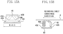
- FIG. 15A is an elevational view of the recording paper surface detection apparatus 40 viewed from the downstream side of the conveyance direction
- Fig. 15B is a side view thereof.
- the incidence surface of the light guide element 45 is provided with a first lens portion 45A and a second lens portion 45B, each having a cross section showing curvature, corresponding to light from the illumination LEDs 42A and 42B, respectively.
- the light beams from the illumination LEDs 42A and 42B are put in parallel with each other by the lens portions 45A and 45B of the light guide element 45, respectively.
- the recording paper surface detection apparatus 40 illustrated in Fig. 15 enables reducing width to about 50% in comparison with that in Fig. 9 (from W to Wx0.5) .
- the lens portions 45A and 45B on the incidence surface of the light guide element 45 are provided with a function for putting light beams in parallel with each other, making it possible to put the diverging light beams from respective illumination LEDs in parallel with each other and radiate the parallel light beams onto the recording sheet obliquely with respect to the surface thereof. Accordingly, it becomes possible to ensure a sufficient light quantity for attaining the improvement in signal-to-noise (S/N) ratio and image forming speed. Thus, shadow reflecting the surface unevenness on the recording sheet can be emphasized.
- S/N signal-to-noise
Applications Claiming Priority (2)
| Application Number | Priority Date | Filing Date | Title |
|---|---|---|---|
| JP2009098145 | 2009-04-14 | ||
| EP10159538.7A EP2241938B1 (fr) | 2009-04-14 | 2010-04-09 | Appareil de formation d'images avec détection de la surface de feuille d'enregistrement |
Related Parent Applications (2)
| Application Number | Title | Priority Date | Filing Date |
|---|---|---|---|
| EP10159538.7A Division EP2241938B1 (fr) | 2009-04-14 | 2010-04-09 | Appareil de formation d'images avec détection de la surface de feuille d'enregistrement |
| EP10159538.7A Division-Into EP2241938B1 (fr) | 2009-04-14 | 2010-04-09 | Appareil de formation d'images avec détection de la surface de feuille d'enregistrement |
Publications (2)
| Publication Number | Publication Date |
|---|---|
| EP3537222A1 true EP3537222A1 (fr) | 2019-09-11 |
| EP3537222B1 EP3537222B1 (fr) | 2022-05-11 |
Family
ID=42335240
Family Applications (2)
| Application Number | Title | Priority Date | Filing Date |
|---|---|---|---|
| EP10159538.7A Active EP2241938B1 (fr) | 2009-04-14 | 2010-04-09 | Appareil de formation d'images avec détection de la surface de feuille d'enregistrement |
| EP19162355.2A Active EP3537222B1 (fr) | 2009-04-14 | 2010-04-09 | Appareil de formation d'images |
Family Applications Before (1)
| Application Number | Title | Priority Date | Filing Date |
|---|---|---|---|
| EP10159538.7A Active EP2241938B1 (fr) | 2009-04-14 | 2010-04-09 | Appareil de formation d'images avec détection de la surface de feuille d'enregistrement |
Country Status (5)
| Country | Link |
|---|---|
| US (2) | US8582116B2 (fr) |
| EP (2) | EP2241938B1 (fr) |
| JP (2) | JP5025756B2 (fr) |
| KR (2) | KR101272126B1 (fr) |
| CN (2) | CN101866126B (fr) |
Families Citing this family (15)
| Publication number | Priority date | Publication date | Assignee | Title |
|---|---|---|---|---|
| US8582116B2 (en) * | 2009-04-14 | 2013-11-12 | Canon Kabushiki Kaisha | Recording sheet surface detection apparatus and image forming apparatus |
| JP5812600B2 (ja) * | 2010-12-10 | 2015-11-17 | キヤノン株式会社 | 画像形成装置 |
| JP5783753B2 (ja) * | 2011-02-18 | 2015-09-24 | キヤノン株式会社 | 記録材判別装置 |
| JP5753409B2 (ja) * | 2011-03-07 | 2015-07-22 | 株式会社トプコン | パノラマ画像作成方法及び3次元レーザスキャナ |
| DE102011078885A1 (de) * | 2011-07-08 | 2013-01-10 | Carl Zeiss Smt Gmbh | Verfahren und Vorrichtung zum Bestimmen der Absorption in einem Rohling |
| JP2014032090A (ja) | 2012-08-02 | 2014-02-20 | Canon Inc | 記録材検知装置及び画像形成装置 |
| JP6103912B2 (ja) * | 2012-12-11 | 2017-03-29 | キヤノン株式会社 | 記録材判別装置及びそれを備えた画像形成装置 |
| JP5825291B2 (ja) | 2013-04-15 | 2015-12-02 | コニカミノルタ株式会社 | 画像形成装置及び基準画像の読取方法 |
| KR102096824B1 (ko) * | 2013-06-24 | 2020-04-06 | 삼성전자주식회사 | 보안 환경을 제공하는 장치 및 방법 |
| US10459388B2 (en) * | 2015-11-19 | 2019-10-29 | Canon Kabushiki Kaisha | Image forming apparatus and recording material determination apparatus |
| EP3523634A1 (fr) * | 2016-10-06 | 2019-08-14 | OCE Holding B.V. | Détection de défauts pour supports d'impression |
| JP6914721B2 (ja) | 2017-05-10 | 2021-08-04 | キヤノン株式会社 | 判別装置及び画像形成装置 |
| JP7003505B2 (ja) * | 2017-09-05 | 2022-01-20 | コニカミノルタ株式会社 | 記録材判別用センサーおよび画像形成装置 |
| JP7325493B2 (ja) | 2021-12-09 | 2023-08-14 | キヤノン株式会社 | 記録材判定装置及び画像形成装置 |
| CN116859690A (zh) * | 2023-07-10 | 2023-10-10 | 虎丘影像(苏州)股份有限公司 | 一种曝光装置 |
Citations (3)
| Publication number | Priority date | Publication date | Assignee | Title |
|---|---|---|---|---|
| WO2003086771A2 (fr) * | 2002-04-11 | 2003-10-23 | Hewlett-Packard Development Company, L.P. | Identification de support d'enregistrement |
| JP2004038879A (ja) | 2002-07-08 | 2004-02-05 | Canon Inc | 映像読取装置及び画像形成装置 |
| US20070076074A1 (en) * | 2005-10-05 | 2007-04-05 | Eastman Kodak Company | Method and apparatus for print medium determination |
Family Cites Families (37)
| Publication number | Priority date | Publication date | Assignee | Title |
|---|---|---|---|---|
| CA1240052A (fr) * | 1984-11-30 | 1988-08-02 | Motoji Shiozumi | Methode et dispositif pour evaluer le degre de brillance d'un objet |
| JPH0541407Y2 (fr) * | 1987-08-11 | 1993-10-20 | ||
| JPH02138805A (ja) * | 1988-08-31 | 1990-05-28 | Canon Inc | 平滑度測定装置およびこれを備えた記録装置 |
| JPH04364451A (ja) | 1991-06-12 | 1992-12-16 | Showa Alum Corp | ワークの表面欠陥検出方法 |
| US5686720A (en) * | 1995-03-02 | 1997-11-11 | Hewlett Packard Company | Method and device for achieving high contrast surface illumination |
| JP3769812B2 (ja) * | 1996-04-11 | 2006-04-26 | 石川島播磨重工業株式会社 | 非接触式速度ベクトル検出装置 |
| JPH1023203A (ja) * | 1996-07-01 | 1998-01-23 | Ricoh Co Ltd | 紙分類装置 |
| JPH10268731A (ja) | 1997-03-27 | 1998-10-09 | Canon Inc | 画像形成装置 |
| JP3406507B2 (ja) * | 1998-03-19 | 2003-05-12 | シャープ株式会社 | 画像形成方法及び画像形成装置 |
| US7283258B1 (en) * | 1998-08-28 | 2007-10-16 | Brother Kogyo Kabushiki Kaisha | Print system capable of notifying user of required ink amount |
| JP2001063870A (ja) | 1999-08-25 | 2001-03-13 | Oki Data Corp | プリンタ装置 |
| US7280258B2 (en) * | 2001-01-05 | 2007-10-09 | Seiko Epson Corporation | Logo data generating system, logo data generating method, and data storage medium |
| JP2003072186A (ja) * | 2001-06-19 | 2003-03-12 | Canon Inc | 画像形成装置及び画像形成方法及びプログラム並びに記録媒体 |
| EP1276065A3 (fr) * | 2001-07-12 | 2004-01-14 | Seiko Epson Corporation | Système de calcul des frais d'impression et système de gestion pour l'approvisionnement de matériaux colorants |
| US7061391B2 (en) * | 2001-10-17 | 2006-06-13 | International Business Machines Corporation | Method, system, and program for monitoring a consumable resource used by a system |
| JP3734247B2 (ja) * | 2002-01-22 | 2006-01-11 | キヤノン株式会社 | 被記録媒体の種類の判別装置、判別方法、および記録装置 |
| JP3919618B2 (ja) * | 2002-07-10 | 2007-05-30 | キヤノン株式会社 | 記録媒体判別方法、プログラム、記憶媒体および記録装置 |
| JP2004139011A (ja) * | 2002-08-20 | 2004-05-13 | Fuji Xerox Co Ltd | 画像処理装置、画像処理方法、および画像処理プログラム |
| JP4993653B2 (ja) * | 2003-10-03 | 2012-08-08 | キヤノン株式会社 | 記録材判別装置および画像形成装置並びにその方法 |
| JP2005234472A (ja) | 2004-02-23 | 2005-09-02 | Canon Inc | 記録材判別装置及び画像形成装置 |
| JP2006058261A (ja) | 2004-08-24 | 2006-03-02 | Seiko Epson Corp | 用紙種類判別装置、用紙種類判別方法および用紙種類判別プログラム |
| KR100612451B1 (ko) * | 2004-10-16 | 2006-08-16 | 삼성전자주식회사 | 화상 형성 장치의 인쇄 매체 인식 장치 및 그 방법 |
| US7695131B2 (en) * | 2004-10-16 | 2010-04-13 | Samsung Electronics Co., Ltd. | Media detection apparatus and method usable with image forming apparatus |
| JP2007057891A (ja) | 2005-08-25 | 2007-03-08 | Canon Inc | 画像形成装置 |
| JP4586725B2 (ja) * | 2005-12-27 | 2010-11-24 | ブラザー工業株式会社 | 監視装置、画像形成装置、画像形成システム |
| US9146513B2 (en) * | 2006-05-15 | 2015-09-29 | Canon Kabushiki Kaisha | Image forming apparatus and image processing method having tone correction |
| JP5203721B2 (ja) * | 2007-01-11 | 2013-06-05 | キヤノン株式会社 | 記録材判別装置及び画像形成装置 |
| US8335442B2 (en) * | 2007-01-30 | 2012-12-18 | Hewlett-Packard Development Company, L.P. | Hard imaging devices and hard imaging methods |
| JP5258323B2 (ja) * | 2008-02-22 | 2013-08-07 | キヤノン株式会社 | 画像形成装置、画像形成装置の制御方法およびプログラム |
| JP5146424B2 (ja) * | 2008-09-13 | 2013-02-20 | 株式会社リコー | 画像処理装置、画像処理方法、プログラム、記録媒体、印刷システム、画像形成装置 |
| JP4440319B2 (ja) * | 2008-10-20 | 2010-03-24 | キヤノン株式会社 | 紙表面検出装置及び画像形成装置 |
| JP5274350B2 (ja) * | 2009-04-14 | 2013-08-28 | キヤノン株式会社 | 記録材表面検出装置及びそれを備える画像形成装置 |
| US8582116B2 (en) * | 2009-04-14 | 2013-11-12 | Canon Kabushiki Kaisha | Recording sheet surface detection apparatus and image forming apparatus |
| JP5553139B2 (ja) * | 2009-08-10 | 2014-07-16 | 富士ゼロックス株式会社 | 画像処理装置、画像処理プログラム |
| JP5423225B2 (ja) * | 2009-08-10 | 2014-02-19 | 富士ゼロックス株式会社 | 画像処理装置、画像処理プログラム |
| JP5365925B2 (ja) * | 2009-09-02 | 2013-12-11 | 富士ゼロックス株式会社 | 画像処理装置、画像処理プログラム |
| US8885214B2 (en) * | 2010-08-31 | 2014-11-11 | Canon Kabushiki Kaisha | Color image processing apparatus which reduces the amount of color materials consumed that are used to form a color image with reference to an index with high utility |
-
2010
- 2010-04-05 US US12/754,454 patent/US8582116B2/en not_active Expired - Fee Related
- 2010-04-08 JP JP2010089581A patent/JP5025756B2/ja active Active
- 2010-04-09 EP EP10159538.7A patent/EP2241938B1/fr active Active
- 2010-04-09 EP EP19162355.2A patent/EP3537222B1/fr active Active
- 2010-04-12 KR KR1020100033095A patent/KR101272126B1/ko active IP Right Grant
- 2010-04-14 CN CN2010101642430A patent/CN101866126B/zh active Active
- 2010-04-14 CN CN201210455685.XA patent/CN102937782B/zh active Active
-
2012
- 2012-06-15 JP JP2012135441A patent/JP5456098B2/ja active Active
- 2012-11-28 KR KR1020120136076A patent/KR101272125B1/ko active IP Right Grant
-
2013
- 2013-10-04 US US14/046,793 patent/US8908193B2/en active Active
Patent Citations (3)
| Publication number | Priority date | Publication date | Assignee | Title |
|---|---|---|---|---|
| WO2003086771A2 (fr) * | 2002-04-11 | 2003-10-23 | Hewlett-Packard Development Company, L.P. | Identification de support d'enregistrement |
| JP2004038879A (ja) | 2002-07-08 | 2004-02-05 | Canon Inc | 映像読取装置及び画像形成装置 |
| US20070076074A1 (en) * | 2005-10-05 | 2007-04-05 | Eastman Kodak Company | Method and apparatus for print medium determination |
Also Published As
| Publication number | Publication date |
|---|---|
| JP5025756B2 (ja) | 2012-09-12 |
| JP2010266432A (ja) | 2010-11-25 |
| CN101866126A (zh) | 2010-10-20 |
| EP3537222B1 (fr) | 2022-05-11 |
| KR101272126B1 (ko) | 2013-06-10 |
| US8582116B2 (en) | 2013-11-12 |
| CN102937782A (zh) | 2013-02-20 |
| KR101272125B1 (ko) | 2013-06-10 |
| CN101866126B (zh) | 2012-12-19 |
| JP2012181555A (ja) | 2012-09-20 |
| JP5456098B2 (ja) | 2014-03-26 |
| CN102937782B (zh) | 2016-01-06 |
| EP2241938A1 (fr) | 2010-10-20 |
| KR20100113982A (ko) | 2010-10-22 |
| US20100259772A1 (en) | 2010-10-14 |
| KR20130008489A (ko) | 2013-01-22 |
| US8908193B2 (en) | 2014-12-09 |
| EP2241938B1 (fr) | 2019-06-12 |
| US20140037310A1 (en) | 2014-02-06 |
Similar Documents
| Publication | Publication Date | Title |
|---|---|---|
| EP3537222B1 (fr) | Appareil de formation d'images | |
| US8131192B2 (en) | Image forming apparatus for forming image on record medium | |
| JP4454914B2 (ja) | 映像読取装置及び画像形成装置 | |
| US8626004B2 (en) | Detecting apparatus and image forming apparatus | |
| US8358446B2 (en) | Reading apparatus, image forming apparatus and image forming method | |
| US9389563B2 (en) | Recording material detecting apparatus and an image-forming apparatus | |
| JP2018179681A (ja) | 光学センサ及び画像形成装置 | |
| JP5546152B2 (ja) | 記録材表面検出装置及びそれを備える画像形成装置 | |
| JP2007156159A (ja) | 色ずれ検出センサ及び色ずれ検出装置 | |
| JP5274350B2 (ja) | 記録材表面検出装置及びそれを備える画像形成装置 | |
| JP2010249614A (ja) | 記録材表面検出装置及びそれを備える画像形成装置 | |
| JP2009271273A (ja) | 記録材表面撮像装置及びそれを備えた画像形成装置 | |
| JP5559392B2 (ja) | 記録材検出装置及びそれを備える画像形成装置 | |
| JP5197311B2 (ja) | 記録材判別装置及びそれを用いた画像形成装置 | |
| JP2012123273A (ja) | 画像形成装置 | |
| US7962074B2 (en) | Developing unit, image forming apparatus, and floating developer collecting method for developing unit | |
| JP2016099625A (ja) | 画像保持面を照らす光導管led発光体 | |
| JP2010273279A (ja) | 画像読取装置及び画像形成装置 | |
| JP2017009955A (ja) | 光走査装置及び該光走査装置を備えた画像形成装置 | |
| JP2002278228A (ja) | 2ドラムカラー画像形成装置 | |
| JP2008058759A (ja) | 光走査装置及び画像形成装置 | |
| JP2006039198A (ja) | カラー画像形成装置 | |
| JP2010230927A (ja) | レジストレーションマーク検出装置、及びこれを用いた画像形成装置 |
Legal Events
| Date | Code | Title | Description |
|---|---|---|---|
| PUAI | Public reference made under article 153(3) epc to a published international application that has entered the european phase |
Free format text: ORIGINAL CODE: 0009012 |
|
| STAA | Information on the status of an ep patent application or granted ep patent |
Free format text: STATUS: THE APPLICATION HAS BEEN PUBLISHED |
|
| AC | Divisional application: reference to earlier application |
Ref document number: 2241938 Country of ref document: EP Kind code of ref document: P |
|
| AK | Designated contracting states |
Kind code of ref document: A1 Designated state(s): AT BE BG CH CY CZ DE DK EE ES FI FR GB GR HR HU IE IS IT LI LT LU LV MC MK MT NL NO PL PT RO SE SI SK SM TR |
|
| STAA | Information on the status of an ep patent application or granted ep patent |
Free format text: STATUS: REQUEST FOR EXAMINATION WAS MADE |
|
| STAA | Information on the status of an ep patent application or granted ep patent |
Free format text: STATUS: EXAMINATION IS IN PROGRESS |
|
| 17P | Request for examination filed |
Effective date: 20200311 |
|
| RBV | Designated contracting states (corrected) |
Designated state(s): AT BE BG CH CY CZ DE DK EE ES FI FR GB GR HR HU IE IS IT LI LT LU LV MC MK MT NL NO PL PT RO SE SI SK SM TR |
|
| 17Q | First examination report despatched |
Effective date: 20200409 |
|
| STAA | Information on the status of an ep patent application or granted ep patent |
Free format text: STATUS: EXAMINATION IS IN PROGRESS |
|
| GRAP | Despatch of communication of intention to grant a patent |
Free format text: ORIGINAL CODE: EPIDOSNIGR1 |
|
| STAA | Information on the status of an ep patent application or granted ep patent |
Free format text: STATUS: GRANT OF PATENT IS INTENDED |
|
| INTG | Intention to grant announced |
Effective date: 20211126 |
|
| GRAS | Grant fee paid |
Free format text: ORIGINAL CODE: EPIDOSNIGR3 |
|
| GRAA | (expected) grant |
Free format text: ORIGINAL CODE: 0009210 |
|
| STAA | Information on the status of an ep patent application or granted ep patent |
Free format text: STATUS: THE PATENT HAS BEEN GRANTED |
|
| AC | Divisional application: reference to earlier application |
Ref document number: 2241938 Country of ref document: EP Kind code of ref document: P |
|
| AK | Designated contracting states |
Kind code of ref document: B1 Designated state(s): AT BE BG CH CY CZ DE DK EE ES FI FR GB GR HR HU IE IS IT LI LT LU LV MC MK MT NL NO PL PT RO SE SI SK SM TR |
|
| REG | Reference to a national code |
Ref country code: GB Ref legal event code: FG4D |
|
| REG | Reference to a national code |
Ref country code: CH Ref legal event code: EP |
|
| REG | Reference to a national code |
Ref country code: AT Ref legal event code: REF Ref document number: 1491957 Country of ref document: AT Kind code of ref document: T Effective date: 20220515 |
|
| REG | Reference to a national code |
Ref country code: DE Ref legal event code: R096 Ref document number: 602010068261 Country of ref document: DE |
|
| REG | Reference to a national code |
Ref country code: IE Ref legal event code: FG4D |
|
| REG | Reference to a national code |
Ref country code: LT Ref legal event code: MG9D |
|
| REG | Reference to a national code |
Ref country code: NL Ref legal event code: MP Effective date: 20220511 |
|
| REG | Reference to a national code |
Ref country code: AT Ref legal event code: MK05 Ref document number: 1491957 Country of ref document: AT Kind code of ref document: T Effective date: 20220511 |
|
| PG25 | Lapsed in a contracting state [announced via postgrant information from national office to epo] |
Ref country code: SE Free format text: LAPSE BECAUSE OF FAILURE TO SUBMIT A TRANSLATION OF THE DESCRIPTION OR TO PAY THE FEE WITHIN THE PRESCRIBED TIME-LIMIT Effective date: 20220511 Ref country code: PT Free format text: LAPSE BECAUSE OF FAILURE TO SUBMIT A TRANSLATION OF THE DESCRIPTION OR TO PAY THE FEE WITHIN THE PRESCRIBED TIME-LIMIT Effective date: 20220912 Ref country code: NO Free format text: LAPSE BECAUSE OF FAILURE TO SUBMIT A TRANSLATION OF THE DESCRIPTION OR TO PAY THE FEE WITHIN THE PRESCRIBED TIME-LIMIT Effective date: 20220811 Ref country code: NL Free format text: LAPSE BECAUSE OF FAILURE TO SUBMIT A TRANSLATION OF THE DESCRIPTION OR TO PAY THE FEE WITHIN THE PRESCRIBED TIME-LIMIT Effective date: 20220511 Ref country code: LT Free format text: LAPSE BECAUSE OF FAILURE TO SUBMIT A TRANSLATION OF THE DESCRIPTION OR TO PAY THE FEE WITHIN THE PRESCRIBED TIME-LIMIT Effective date: 20220511 Ref country code: HR Free format text: LAPSE BECAUSE OF FAILURE TO SUBMIT A TRANSLATION OF THE DESCRIPTION OR TO PAY THE FEE WITHIN THE PRESCRIBED TIME-LIMIT Effective date: 20220511 Ref country code: GR Free format text: LAPSE BECAUSE OF FAILURE TO SUBMIT A TRANSLATION OF THE DESCRIPTION OR TO PAY THE FEE WITHIN THE PRESCRIBED TIME-LIMIT Effective date: 20220812 Ref country code: FI Free format text: LAPSE BECAUSE OF FAILURE TO SUBMIT A TRANSLATION OF THE DESCRIPTION OR TO PAY THE FEE WITHIN THE PRESCRIBED TIME-LIMIT Effective date: 20220511 Ref country code: ES Free format text: LAPSE BECAUSE OF FAILURE TO SUBMIT A TRANSLATION OF THE DESCRIPTION OR TO PAY THE FEE WITHIN THE PRESCRIBED TIME-LIMIT Effective date: 20220511 Ref country code: BG Free format text: LAPSE BECAUSE OF FAILURE TO SUBMIT A TRANSLATION OF THE DESCRIPTION OR TO PAY THE FEE WITHIN THE PRESCRIBED TIME-LIMIT Effective date: 20220811 Ref country code: AT Free format text: LAPSE BECAUSE OF FAILURE TO SUBMIT A TRANSLATION OF THE DESCRIPTION OR TO PAY THE FEE WITHIN THE PRESCRIBED TIME-LIMIT Effective date: 20220511 |
|
| PG25 | Lapsed in a contracting state [announced via postgrant information from national office to epo] |
Ref country code: PL Free format text: LAPSE BECAUSE OF FAILURE TO SUBMIT A TRANSLATION OF THE DESCRIPTION OR TO PAY THE FEE WITHIN THE PRESCRIBED TIME-LIMIT Effective date: 20220511 Ref country code: LV Free format text: LAPSE BECAUSE OF FAILURE TO SUBMIT A TRANSLATION OF THE DESCRIPTION OR TO PAY THE FEE WITHIN THE PRESCRIBED TIME-LIMIT Effective date: 20220511 Ref country code: IS Free format text: LAPSE BECAUSE OF FAILURE TO SUBMIT A TRANSLATION OF THE DESCRIPTION OR TO PAY THE FEE WITHIN THE PRESCRIBED TIME-LIMIT Effective date: 20220911 |
|
| PG25 | Lapsed in a contracting state [announced via postgrant information from national office to epo] |
Ref country code: SM Free format text: LAPSE BECAUSE OF FAILURE TO SUBMIT A TRANSLATION OF THE DESCRIPTION OR TO PAY THE FEE WITHIN THE PRESCRIBED TIME-LIMIT Effective date: 20220511 Ref country code: SK Free format text: LAPSE BECAUSE OF FAILURE TO SUBMIT A TRANSLATION OF THE DESCRIPTION OR TO PAY THE FEE WITHIN THE PRESCRIBED TIME-LIMIT Effective date: 20220511 Ref country code: RO Free format text: LAPSE BECAUSE OF FAILURE TO SUBMIT A TRANSLATION OF THE DESCRIPTION OR TO PAY THE FEE WITHIN THE PRESCRIBED TIME-LIMIT Effective date: 20220511 Ref country code: EE Free format text: LAPSE BECAUSE OF FAILURE TO SUBMIT A TRANSLATION OF THE DESCRIPTION OR TO PAY THE FEE WITHIN THE PRESCRIBED TIME-LIMIT Effective date: 20220511 Ref country code: DK Free format text: LAPSE BECAUSE OF FAILURE TO SUBMIT A TRANSLATION OF THE DESCRIPTION OR TO PAY THE FEE WITHIN THE PRESCRIBED TIME-LIMIT Effective date: 20220511 Ref country code: CZ Free format text: LAPSE BECAUSE OF FAILURE TO SUBMIT A TRANSLATION OF THE DESCRIPTION OR TO PAY THE FEE WITHIN THE PRESCRIBED TIME-LIMIT Effective date: 20220511 |
|
| REG | Reference to a national code |
Ref country code: DE Ref legal event code: R097 Ref document number: 602010068261 Country of ref document: DE |
|
| PLBE | No opposition filed within time limit |
Free format text: ORIGINAL CODE: 0009261 |
|
| STAA | Information on the status of an ep patent application or granted ep patent |
Free format text: STATUS: NO OPPOSITION FILED WITHIN TIME LIMIT |
|
| 26N | No opposition filed |
Effective date: 20230214 |
|
| PG25 | Lapsed in a contracting state [announced via postgrant information from national office to epo] |
Ref country code: SI Free format text: LAPSE BECAUSE OF FAILURE TO SUBMIT A TRANSLATION OF THE DESCRIPTION OR TO PAY THE FEE WITHIN THE PRESCRIBED TIME-LIMIT Effective date: 20220511 |
|
| PGFP | Annual fee paid to national office [announced via postgrant information from national office to epo] |
Ref country code: GB Payment date: 20230321 Year of fee payment: 14 |
|
| PGFP | Annual fee paid to national office [announced via postgrant information from national office to epo] |
Ref country code: DE Payment date: 20230321 Year of fee payment: 14 |
|
| REG | Reference to a national code |
Ref country code: CH Ref legal event code: PL |
|
| PG25 | Lapsed in a contracting state [announced via postgrant information from national office to epo] |
Ref country code: LU Free format text: LAPSE BECAUSE OF NON-PAYMENT OF DUE FEES Effective date: 20230409 |
|
| REG | Reference to a national code |
Ref country code: BE Ref legal event code: MM Effective date: 20230430 |
|
| PG25 | Lapsed in a contracting state [announced via postgrant information from national office to epo] |
Ref country code: MC Free format text: LAPSE BECAUSE OF FAILURE TO SUBMIT A TRANSLATION OF THE DESCRIPTION OR TO PAY THE FEE WITHIN THE PRESCRIBED TIME-LIMIT Effective date: 20220511 |
|
| PG25 | Lapsed in a contracting state [announced via postgrant information from national office to epo] |
Ref country code: MC Free format text: LAPSE BECAUSE OF FAILURE TO SUBMIT A TRANSLATION OF THE DESCRIPTION OR TO PAY THE FEE WITHIN THE PRESCRIBED TIME-LIMIT Effective date: 20220511 Ref country code: LI Free format text: LAPSE BECAUSE OF NON-PAYMENT OF DUE FEES Effective date: 20230430 Ref country code: IT Free format text: LAPSE BECAUSE OF FAILURE TO SUBMIT A TRANSLATION OF THE DESCRIPTION OR TO PAY THE FEE WITHIN THE PRESCRIBED TIME-LIMIT Effective date: 20220511 Ref country code: FR Free format text: LAPSE BECAUSE OF NON-PAYMENT OF DUE FEES Effective date: 20230430 Ref country code: CH Free format text: LAPSE BECAUSE OF NON-PAYMENT OF DUE FEES Effective date: 20230430 |
|
| REG | Reference to a national code |
Ref country code: IE Ref legal event code: MM4A |
|
| PG25 | Lapsed in a contracting state [announced via postgrant information from national office to epo] |
Ref country code: BE Free format text: LAPSE BECAUSE OF NON-PAYMENT OF DUE FEES Effective date: 20230430 |
|
| PG25 | Lapsed in a contracting state [announced via postgrant information from national office to epo] |
Ref country code: IE Free format text: LAPSE BECAUSE OF NON-PAYMENT OF DUE FEES Effective date: 20230409 |