EP3471402B1 - Integrierte vorrichtung zur temporären gruppierung von empfangenen photonen - Google Patents
Integrierte vorrichtung zur temporären gruppierung von empfangenen photonen Download PDFInfo
- Publication number
- EP3471402B1 EP3471402B1 EP18202357.2A EP18202357A EP3471402B1 EP 3471402 B1 EP3471402 B1 EP 3471402B1 EP 18202357 A EP18202357 A EP 18202357A EP 3471402 B1 EP3471402 B1 EP 3471402B1
- Authority
- EP
- European Patent Office
- Prior art keywords
- time
- charge
- charge carrier
- region
- carrier
- Prior art date
- Legal status (The legal status is an assumption and is not a legal conclusion. Google has not performed a legal analysis and makes no representation as to the accuracy of the status listed.)
- Active
Links
- 230000002123 temporal effect Effects 0.000 title description 32
- 239000002800 charge carrier Substances 0.000 claims description 205
- 238000005036 potential barrier Methods 0.000 claims description 57
- 230000004044 response Effects 0.000 claims description 36
- 150000007523 nucleic acids Chemical class 0.000 claims description 29
- 238000005204 segregation Methods 0.000 claims description 29
- 108020004707 nucleic acids Proteins 0.000 claims description 28
- 102000039446 nucleic acids Human genes 0.000 claims description 28
- 238000004458 analytical method Methods 0.000 claims description 19
- 239000004065 semiconductor Substances 0.000 claims description 18
- 239000000463 material Substances 0.000 claims description 13
- 238000000034 method Methods 0.000 description 107
- 238000005259 measurement Methods 0.000 description 98
- 239000000523 sample Substances 0.000 description 89
- 230000005284 excitation Effects 0.000 description 78
- 239000003990 capacitor Substances 0.000 description 56
- 238000010521 absorption reaction Methods 0.000 description 55
- 238000003384 imaging method Methods 0.000 description 37
- 239000003550 marker Substances 0.000 description 37
- 239000002184 metal Substances 0.000 description 33
- 238000009792 diffusion process Methods 0.000 description 32
- 239000000969 carrier Substances 0.000 description 29
- 238000010586 diagram Methods 0.000 description 29
- 238000001514 detection method Methods 0.000 description 27
- 230000000875 corresponding effect Effects 0.000 description 26
- 238000012546 transfer Methods 0.000 description 23
- 230000008569 process Effects 0.000 description 21
- 238000005070 sampling Methods 0.000 description 19
- 230000005684 electric field Effects 0.000 description 18
- 239000002773 nucleotide Substances 0.000 description 18
- 125000003729 nucleotide group Chemical group 0.000 description 18
- 229910021420 polycrystalline silicon Inorganic materials 0.000 description 18
- 229920005591 polysilicon Polymers 0.000 description 18
- 239000000758 substrate Substances 0.000 description 18
- 230000003247 decreasing effect Effects 0.000 description 17
- 238000004020 luminiscence type Methods 0.000 description 15
- 230000003287 optical effect Effects 0.000 description 15
- 238000012163 sequencing technique Methods 0.000 description 15
- 230000008859 change Effects 0.000 description 13
- 230000006870 function Effects 0.000 description 13
- 230000015572 biosynthetic process Effects 0.000 description 12
- 101150049912 bin3 gene Proteins 0.000 description 11
- 230000003071 parasitic effect Effects 0.000 description 10
- 230000007423 decrease Effects 0.000 description 9
- 230000003595 spectral effect Effects 0.000 description 9
- 230000002596 correlated effect Effects 0.000 description 8
- 239000007943 implant Substances 0.000 description 8
- 238000001712 DNA sequencing Methods 0.000 description 7
- XUIMIQQOPSSXEZ-UHFFFAOYSA-N Silicon Chemical compound [Si] XUIMIQQOPSSXEZ-UHFFFAOYSA-N 0.000 description 7
- 238000004166 bioassay Methods 0.000 description 7
- 238000006243 chemical reaction Methods 0.000 description 7
- 229910052710 silicon Inorganic materials 0.000 description 7
- 239000010703 silicon Substances 0.000 description 7
- 108020004414 DNA Proteins 0.000 description 6
- 230000004931 aggregating effect Effects 0.000 description 6
- 238000002372 labelling Methods 0.000 description 6
- 206010028980 Neoplasm Diseases 0.000 description 5
- 229910019142 PO4 Inorganic materials 0.000 description 5
- 230000000295 complement effect Effects 0.000 description 5
- 238000004590 computer program Methods 0.000 description 5
- 235000021317 phosphate Nutrition 0.000 description 5
- 102000016928 DNA-directed DNA polymerase Human genes 0.000 description 4
- 108010014303 DNA-directed DNA polymerase Proteins 0.000 description 4
- 102000004190 Enzymes Human genes 0.000 description 4
- 108090000790 Enzymes Proteins 0.000 description 4
- 238000012512 characterization method Methods 0.000 description 4
- 239000004020 conductor Substances 0.000 description 4
- 230000001276 controlling effect Effects 0.000 description 4
- OPTASPLRGRRNAP-UHFFFAOYSA-N cytosine Chemical compound NC=1C=CNC(=O)N=1 OPTASPLRGRRNAP-UHFFFAOYSA-N 0.000 description 4
- 238000007599 discharging Methods 0.000 description 4
- 239000002019 doping agent Substances 0.000 description 4
- 238000005516 engineering process Methods 0.000 description 4
- 238000001914 filtration Methods 0.000 description 4
- UYTPUPDQBNUYGX-UHFFFAOYSA-N guanine Chemical compound O=C1NC(N)=NC2=C1N=CN2 UYTPUPDQBNUYGX-UHFFFAOYSA-N 0.000 description 4
- 238000004519 manufacturing process Methods 0.000 description 4
- 238000012544 monitoring process Methods 0.000 description 4
- 239000010452 phosphate Substances 0.000 description 4
- 238000012545 processing Methods 0.000 description 4
- 238000001228 spectrum Methods 0.000 description 4
- RWQNBRDOKXIBIV-UHFFFAOYSA-N thymine Chemical compound CC1=CNC(=O)NC1=O RWQNBRDOKXIBIV-UHFFFAOYSA-N 0.000 description 4
- -1 contact Inorganic materials 0.000 description 3
- 238000013461 design Methods 0.000 description 3
- 230000000694 effects Effects 0.000 description 3
- 238000000295 emission spectrum Methods 0.000 description 3
- 230000005281 excited state Effects 0.000 description 3
- 238000010348 incorporation Methods 0.000 description 3
- 150000002632 lipids Chemical class 0.000 description 3
- 230000000737 periodic effect Effects 0.000 description 3
- NBIIXXVUZAFLBC-UHFFFAOYSA-K phosphate Chemical compound [O-]P([O-])([O-])=O NBIIXXVUZAFLBC-UHFFFAOYSA-K 0.000 description 3
- 102000004169 proteins and genes Human genes 0.000 description 3
- 108090000623 proteins and genes Proteins 0.000 description 3
- 238000005215 recombination Methods 0.000 description 3
- 230000006798 recombination Effects 0.000 description 3
- 230000003068 static effect Effects 0.000 description 3
- 239000000126 substance Substances 0.000 description 3
- 238000012360 testing method Methods 0.000 description 3
- 230000007704 transition Effects 0.000 description 3
- YBJHBAHKTGYVGT-ZKWXMUAHSA-N (+)-Biotin Chemical compound N1C(=O)N[C@@H]2[C@H](CCCCC(=O)O)SC[C@@H]21 YBJHBAHKTGYVGT-ZKWXMUAHSA-N 0.000 description 2
- GFFGJBXGBJISGV-UHFFFAOYSA-N Adenine Chemical compound NC1=NC=NC2=C1N=CN2 GFFGJBXGBJISGV-UHFFFAOYSA-N 0.000 description 2
- 229930024421 Adenine Natural products 0.000 description 2
- 238000012935 Averaging Methods 0.000 description 2
- 102000053602 DNA Human genes 0.000 description 2
- VYPSYNLAJGMNEJ-UHFFFAOYSA-N Silicium dioxide Chemical compound O=[Si]=O VYPSYNLAJGMNEJ-UHFFFAOYSA-N 0.000 description 2
- 230000003044 adaptive effect Effects 0.000 description 2
- 229960000643 adenine Drugs 0.000 description 2
- 230000003321 amplification Effects 0.000 description 2
- 238000003491 array Methods 0.000 description 2
- 230000004888 barrier function Effects 0.000 description 2
- 229940104302 cytosine Drugs 0.000 description 2
- 238000002596 diffuse optical imaging Methods 0.000 description 2
- 238000002292 fluorescence lifetime imaging microscopy Methods 0.000 description 2
- 238000002866 fluorescence resonance energy transfer Methods 0.000 description 2
- 239000007850 fluorescent dye Substances 0.000 description 2
- 125000000524 functional group Chemical group 0.000 description 2
- 229910044991 metal oxide Inorganic materials 0.000 description 2
- 150000004706 metal oxides Chemical class 0.000 description 2
- 239000000203 mixture Substances 0.000 description 2
- 229930027945 nicotinamide-adenine dinucleotide Natural products 0.000 description 2
- BOPGDPNILDQYTO-NNYOXOHSSA-N nicotinamide-adenine dinucleotide Chemical compound C1=CCC(C(=O)N)=CN1[C@H]1[C@H](O)[C@H](O)[C@@H](COP(O)(=O)OP(O)(=O)OC[C@@H]2[C@H]([C@@H](O)[C@@H](O2)N2C3=NC=NC(N)=C3N=C2)O)O1 BOPGDPNILDQYTO-NNYOXOHSSA-N 0.000 description 2
- 238000003199 nucleic acid amplification method Methods 0.000 description 2
- 229910052814 silicon oxide Inorganic materials 0.000 description 2
- 238000001356 surgical procedure Methods 0.000 description 2
- 229940113082 thymine Drugs 0.000 description 2
- 102000008186 Collagen Human genes 0.000 description 1
- 108010035532 Collagen Proteins 0.000 description 1
- 102000004594 DNA Polymerase I Human genes 0.000 description 1
- 108010017826 DNA Polymerase I Proteins 0.000 description 1
- 102000016942 Elastin Human genes 0.000 description 1
- 108010014258 Elastin Proteins 0.000 description 1
- 241000588724 Escherichia coli Species 0.000 description 1
- 241000701533 Escherichia virus T4 Species 0.000 description 1
- 108010054147 Hemoglobins Proteins 0.000 description 1
- 102000001554 Hemoglobins Human genes 0.000 description 1
- 102000011782 Keratins Human genes 0.000 description 1
- 108010076876 Keratins Proteins 0.000 description 1
- 102100030569 Nuclear receptor corepressor 2 Human genes 0.000 description 1
- 101710153660 Nuclear receptor corepressor 2 Proteins 0.000 description 1
- 108091028043 Nucleic acid sequence Proteins 0.000 description 1
- 108010064719 Oxyhemoglobins Proteins 0.000 description 1
- 238000003559 RNA-seq method Methods 0.000 description 1
- 108020004682 Single-Stranded DNA Proteins 0.000 description 1
- 230000002159 abnormal effect Effects 0.000 description 1
- 238000009825 accumulation Methods 0.000 description 1
- 150000001413 amino acids Chemical class 0.000 description 1
- 238000003556 assay Methods 0.000 description 1
- 230000008901 benefit Effects 0.000 description 1
- 239000012472 biological sample Substances 0.000 description 1
- 229960002685 biotin Drugs 0.000 description 1
- 235000020958 biotin Nutrition 0.000 description 1
- 239000011616 biotin Substances 0.000 description 1
- 201000011510 cancer Diseases 0.000 description 1
- 230000001413 cellular effect Effects 0.000 description 1
- 238000010516 chain-walking reaction Methods 0.000 description 1
- 229920001436 collagen Polymers 0.000 description 1
- 230000001186 cumulative effect Effects 0.000 description 1
- 239000005549 deoxyribonucleoside Substances 0.000 description 1
- 238000009543 diffuse optical tomography Methods 0.000 description 1
- 239000000975 dye Substances 0.000 description 1
- 229920002549 elastin Polymers 0.000 description 1
- 238000001839 endoscopy Methods 0.000 description 1
- 230000002255 enzymatic effect Effects 0.000 description 1
- 238000005530 etching Methods 0.000 description 1
- 238000002474 experimental method Methods 0.000 description 1
- FVTCRASFADXXNN-SCRDCRAPSA-N flavin mononucleotide Chemical compound OP(=O)(O)OC[C@@H](O)[C@@H](O)[C@@H](O)CN1C=2C=C(C)C(C)=CC=2N=C2C1=NC(=O)NC2=O FVTCRASFADXXNN-SCRDCRAPSA-N 0.000 description 1
- 150000002211 flavins Chemical class 0.000 description 1
- 102000034287 fluorescent proteins Human genes 0.000 description 1
- 108091006047 fluorescent proteins Proteins 0.000 description 1
- 210000001035 gastrointestinal tract Anatomy 0.000 description 1
- 238000009396 hybridization Methods 0.000 description 1
- 125000002887 hydroxy group Chemical group [H]O* 0.000 description 1
- 238000013275 image-guided biopsy Methods 0.000 description 1
- 238000002675 image-guided surgery Methods 0.000 description 1
- 239000011810 insulating material Substances 0.000 description 1
- 239000012212 insulator Substances 0.000 description 1
- 230000010354 integration Effects 0.000 description 1
- 150000002500 ions Chemical class 0.000 description 1
- 230000003902 lesion Effects 0.000 description 1
- 239000003446 ligand Substances 0.000 description 1
- 230000003211 malignant effect Effects 0.000 description 1
- 238000013507 mapping Methods 0.000 description 1
- 239000012528 membrane Substances 0.000 description 1
- 230000004066 metabolic change Effects 0.000 description 1
- 230000002503 metabolic effect Effects 0.000 description 1
- 238000001000 micrograph Methods 0.000 description 1
- 238000000386 microscopy Methods 0.000 description 1
- 238000000329 molecular dynamics simulation Methods 0.000 description 1
- 230000004001 molecular interaction Effects 0.000 description 1
- 239000003068 molecular probe Substances 0.000 description 1
- 229910021421 monocrystalline silicon Inorganic materials 0.000 description 1
- 238000006213 oxygenation reaction Methods 0.000 description 1
- 125000002467 phosphate group Chemical group [H]OP(=O)(O[H])O[*] 0.000 description 1
- 150000003013 phosphoric acid derivatives Chemical class 0.000 description 1
- 230000002250 progressing effect Effects 0.000 description 1
- 230000004850 protein–protein interaction Effects 0.000 description 1
- 238000004445 quantitative analysis Methods 0.000 description 1
- 239000002096 quantum dot Substances 0.000 description 1
- 230000009467 reduction Effects 0.000 description 1
- 238000011160 research Methods 0.000 description 1
- 238000002271 resection Methods 0.000 description 1
- 238000012216 screening Methods 0.000 description 1
- 230000035945 sensitivity Effects 0.000 description 1
- 239000007787 solid Substances 0.000 description 1
- 238000010408 sweeping Methods 0.000 description 1
- 238000001308 synthesis method Methods 0.000 description 1
- 238000003786 synthesis reaction Methods 0.000 description 1
- 230000002194 synthesizing effect Effects 0.000 description 1
- 239000003826 tablet Substances 0.000 description 1
- 238000002366 time-of-flight method Methods 0.000 description 1
- 239000001226 triphosphate Substances 0.000 description 1
- 235000011178 triphosphate Nutrition 0.000 description 1
- 125000002264 triphosphate group Chemical class [H]OP(=O)(O[H])OP(=O)(O[H])OP(=O)(O[H])O* 0.000 description 1
Images


Classifications
-
- H—ELECTRICITY
- H01—ELECTRIC ELEMENTS
- H01L—SEMICONDUCTOR DEVICES NOT COVERED BY CLASS H10
- H01L27/00—Devices consisting of a plurality of semiconductor or other solid-state components formed in or on a common substrate
- H01L27/14—Devices consisting of a plurality of semiconductor or other solid-state components formed in or on a common substrate including semiconductor components sensitive to infrared radiation, light, electromagnetic radiation of shorter wavelength or corpuscular radiation and specially adapted either for the conversion of the energy of such radiation into electrical energy or for the control of electrical energy by such radiation
- H01L27/144—Devices controlled by radiation
- H01L27/146—Imager structures
- H01L27/14601—Structural or functional details thereof
- H01L27/14603—Special geometry or disposition of pixel-elements, address-lines or gate-electrodes
-
- G—PHYSICS
- G01—MEASURING; TESTING
- G01N—INVESTIGATING OR ANALYSING MATERIALS BY DETERMINING THEIR CHEMICAL OR PHYSICAL PROPERTIES
- G01N21/00—Investigating or analysing materials by the use of optical means, i.e. using sub-millimetre waves, infrared, visible or ultraviolet light
- G01N21/62—Systems in which the material investigated is excited whereby it emits light or causes a change in wavelength of the incident light
- G01N21/63—Systems in which the material investigated is excited whereby it emits light or causes a change in wavelength of the incident light optically excited
- G01N21/64—Fluorescence; Phosphorescence
- G01N21/6428—Measuring fluorescence of fluorescent products of reactions or of fluorochrome labelled reactive substances, e.g. measuring quenching effects, using measuring "optrodes"
-
- C—CHEMISTRY; METALLURGY
- C12—BIOCHEMISTRY; BEER; SPIRITS; WINE; VINEGAR; MICROBIOLOGY; ENZYMOLOGY; MUTATION OR GENETIC ENGINEERING
- C12Q—MEASURING OR TESTING PROCESSES INVOLVING ENZYMES, NUCLEIC ACIDS OR MICROORGANISMS; COMPOSITIONS OR TEST PAPERS THEREFOR; PROCESSES OF PREPARING SUCH COMPOSITIONS; CONDITION-RESPONSIVE CONTROL IN MICROBIOLOGICAL OR ENZYMOLOGICAL PROCESSES
- C12Q1/00—Measuring or testing processes involving enzymes, nucleic acids or microorganisms; Compositions therefor; Processes of preparing such compositions
- C12Q1/68—Measuring or testing processes involving enzymes, nucleic acids or microorganisms; Compositions therefor; Processes of preparing such compositions involving nucleic acids
- C12Q1/6869—Methods for sequencing
-
- G—PHYSICS
- G01—MEASURING; TESTING
- G01J—MEASUREMENT OF INTENSITY, VELOCITY, SPECTRAL CONTENT, POLARISATION, PHASE OR PULSE CHARACTERISTICS OF INFRARED, VISIBLE OR ULTRAVIOLET LIGHT; COLORIMETRY; RADIATION PYROMETRY
- G01J3/00—Spectrometry; Spectrophotometry; Monochromators; Measuring colours
- G01J3/28—Investigating the spectrum
- G01J3/44—Raman spectrometry; Scattering spectrometry ; Fluorescence spectrometry
- G01J3/4406—Fluorescence spectrometry
-
- G—PHYSICS
- G01—MEASURING; TESTING
- G01N—INVESTIGATING OR ANALYSING MATERIALS BY DETERMINING THEIR CHEMICAL OR PHYSICAL PROPERTIES
- G01N21/00—Investigating or analysing materials by the use of optical means, i.e. using sub-millimetre waves, infrared, visible or ultraviolet light
- G01N21/62—Systems in which the material investigated is excited whereby it emits light or causes a change in wavelength of the incident light
- G01N21/63—Systems in which the material investigated is excited whereby it emits light or causes a change in wavelength of the incident light optically excited
- G01N21/64—Fluorescence; Phosphorescence
- G01N21/6408—Fluorescence; Phosphorescence with measurement of decay time, time resolved fluorescence
-
- G—PHYSICS
- G01—MEASURING; TESTING
- G01N—INVESTIGATING OR ANALYSING MATERIALS BY DETERMINING THEIR CHEMICAL OR PHYSICAL PROPERTIES
- G01N21/00—Investigating or analysing materials by the use of optical means, i.e. using sub-millimetre waves, infrared, visible or ultraviolet light
- G01N21/62—Systems in which the material investigated is excited whereby it emits light or causes a change in wavelength of the incident light
- G01N21/63—Systems in which the material investigated is excited whereby it emits light or causes a change in wavelength of the incident light optically excited
- G01N21/64—Fluorescence; Phosphorescence
- G01N21/645—Specially adapted constructive features of fluorimeters
- G01N21/6456—Spatial resolved fluorescence measurements; Imaging
- G01N21/6458—Fluorescence microscopy
-
- G—PHYSICS
- G01—MEASURING; TESTING
- G01S—RADIO DIRECTION-FINDING; RADIO NAVIGATION; DETERMINING DISTANCE OR VELOCITY BY USE OF RADIO WAVES; LOCATING OR PRESENCE-DETECTING BY USE OF THE REFLECTION OR RERADIATION OF RADIO WAVES; ANALOGOUS ARRANGEMENTS USING OTHER WAVES
- G01S7/00—Details of systems according to groups G01S13/00, G01S15/00, G01S17/00
- G01S7/48—Details of systems according to groups G01S13/00, G01S15/00, G01S17/00 of systems according to group G01S17/00
- G01S7/483—Details of pulse systems
- G01S7/486—Receivers
- G01S7/4865—Time delay measurement, e.g. time-of-flight measurement, time of arrival measurement or determining the exact position of a peak
-
- H—ELECTRICITY
- H01—ELECTRIC ELEMENTS
- H01L—SEMICONDUCTOR DEVICES NOT COVERED BY CLASS H10
- H01L27/00—Devices consisting of a plurality of semiconductor or other solid-state components formed in or on a common substrate
- H01L27/14—Devices consisting of a plurality of semiconductor or other solid-state components formed in or on a common substrate including semiconductor components sensitive to infrared radiation, light, electromagnetic radiation of shorter wavelength or corpuscular radiation and specially adapted either for the conversion of the energy of such radiation into electrical energy or for the control of electrical energy by such radiation
- H01L27/144—Devices controlled by radiation
- H01L27/146—Imager structures
- H01L27/14683—Processes or apparatus peculiar to the manufacture or treatment of these devices or parts thereof
- H01L27/14687—Wafer level processing
-
- H—ELECTRICITY
- H01—ELECTRIC ELEMENTS
- H01L—SEMICONDUCTOR DEVICES NOT COVERED BY CLASS H10
- H01L27/00—Devices consisting of a plurality of semiconductor or other solid-state components formed in or on a common substrate
- H01L27/14—Devices consisting of a plurality of semiconductor or other solid-state components formed in or on a common substrate including semiconductor components sensitive to infrared radiation, light, electromagnetic radiation of shorter wavelength or corpuscular radiation and specially adapted either for the conversion of the energy of such radiation into electrical energy or for the control of electrical energy by such radiation
- H01L27/144—Devices controlled by radiation
- H01L27/146—Imager structures
- H01L27/148—Charge coupled imagers
- H01L27/14806—Structural or functional details thereof
- H01L27/14812—Special geometry or disposition of pixel-elements, address lines or gate-electrodes
-
- G—PHYSICS
- G01—MEASURING; TESTING
- G01N—INVESTIGATING OR ANALYSING MATERIALS BY DETERMINING THEIR CHEMICAL OR PHYSICAL PROPERTIES
- G01N21/00—Investigating or analysing materials by the use of optical means, i.e. using sub-millimetre waves, infrared, visible or ultraviolet light
- G01N21/62—Systems in which the material investigated is excited whereby it emits light or causes a change in wavelength of the incident light
- G01N21/63—Systems in which the material investigated is excited whereby it emits light or causes a change in wavelength of the incident light optically excited
- G01N21/64—Fluorescence; Phosphorescence
- G01N21/6428—Measuring fluorescence of fluorescent products of reactions or of fluorochrome labelled reactive substances, e.g. measuring quenching effects, using measuring "optrodes"
- G01N2021/6439—Measuring fluorescence of fluorescent products of reactions or of fluorochrome labelled reactive substances, e.g. measuring quenching effects, using measuring "optrodes" with indicators, stains, dyes, tags, labels, marks
- G01N2021/6441—Measuring fluorescence of fluorescent products of reactions or of fluorochrome labelled reactive substances, e.g. measuring quenching effects, using measuring "optrodes" with indicators, stains, dyes, tags, labels, marks with two or more labels
-
- G—PHYSICS
- G01—MEASURING; TESTING
- G01N—INVESTIGATING OR ANALYSING MATERIALS BY DETERMINING THEIR CHEMICAL OR PHYSICAL PROPERTIES
- G01N2201/00—Features of devices classified in G01N21/00
- G01N2201/06—Illumination; Optics
- G01N2201/061—Sources
- G01N2201/06113—Coherent sources; lasers
-
- G—PHYSICS
- G01—MEASURING; TESTING
- G01N—INVESTIGATING OR ANALYSING MATERIALS BY DETERMINING THEIR CHEMICAL OR PHYSICAL PROPERTIES
- G01N2201/00—Features of devices classified in G01N21/00
- G01N2201/06—Illumination; Optics
- G01N2201/069—Supply of sources
- G01N2201/0696—Pulsed
- G01N2201/0697—Pulsed lasers
-
- G—PHYSICS
- G01—MEASURING; TESTING
- G01S—RADIO DIRECTION-FINDING; RADIO NAVIGATION; DETERMINING DISTANCE OR VELOCITY BY USE OF RADIO WAVES; LOCATING OR PRESENCE-DETECTING BY USE OF THE REFLECTION OR RERADIATION OF RADIO WAVES; ANALOGOUS ARRANGEMENTS USING OTHER WAVES
- G01S17/00—Systems using the reflection or reradiation of electromagnetic waves other than radio waves, e.g. lidar systems
- G01S17/88—Lidar systems specially adapted for specific applications
- G01S17/89—Lidar systems specially adapted for specific applications for mapping or imaging
- G01S17/894—3D imaging with simultaneous measurement of time-of-flight at a 2D array of receiver pixels, e.g. time-of-flight cameras or flash lidar
-
- G—PHYSICS
- G01—MEASURING; TESTING
- G01S—RADIO DIRECTION-FINDING; RADIO NAVIGATION; DETERMINING DISTANCE OR VELOCITY BY USE OF RADIO WAVES; LOCATING OR PRESENCE-DETECTING BY USE OF THE REFLECTION OR RERADIATION OF RADIO WAVES; ANALOGOUS ARRANGEMENTS USING OTHER WAVES
- G01S7/00—Details of systems according to groups G01S13/00, G01S15/00, G01S17/00
- G01S7/48—Details of systems according to groups G01S13/00, G01S15/00, G01S17/00 of systems according to group G01S17/00
- G01S7/483—Details of pulse systems
- G01S7/486—Receivers
- G01S7/4861—Circuits for detection, sampling, integration or read-out
- G01S7/4863—Detector arrays, e.g. charge-transfer gates
Definitions
- Photodetectors are used to detect light in a variety of applications. Integrated photodetectors have been developed that produce an electrical signal indicative of the intensity of incident light. Integrated photodetectors for imaging applications include an array of pixels to detect the intensity of light received from across a scene. Examples of integrated photodetectors include charge coupled devices (CCDs) and Complementary Metal Oxide Semiconductor (CMOS) image sensors.
- CCDs charge coupled devices
- CMOS Complementary Metal Oxide Semiconductor
- WO 2011/103507 A1 describes optics collection and detection systems for measuring optical signals from an array of optical sources over time.
- WO 2010/025331 A1 describes a demodulation pixel with daisy chain charge storage sites.
- EP 2 182 523 A1 describes a charge sampling device.
- an integrated photodetector that can accurately measure, or "time-bin," the timing of arrival of incident photons.
- the integrated photodetector can measure the arrival of photons with nanosecond or picosecond resolution.
- Such a photodetector may find application in a variety of applications including molecular detection/quantiation, which may be applied to sequencing of nucleic acids (e.g., DNA sequencing).
- Such a photodetector can facilitate time-domain analysis of the arrival of incident photons from luminescent molecules used to label nucleotides, thereby enabling identification and sequencing of nucleotides based upon luminance lifetimes.
- Other examples of applications of the integrated photodetector include fluorescence lifetime imaging and time-of-flight imaging, as discussed further below.
- Bioassays conventionally involve large, expensive laboratory equipment requiring research scientists trained to operate the equipment and perform the bioassays. Bioassays are conventionally performed in bulk such that a large amount of a particular type of sample is necessary for detection and quantitation. Some bioassays are performed by tagging samples with luminescent markers that emit light of a particular wavelength. The samples are illuminated with a light source to cause luminescence, and the luminescent light is detected with a photodetector to quantify the amount of light emitted by the markers. Bioassays using luminescent tags and/or reporters conventionally involve expensive laser light sources to illuminate samples and complicated luminescent detection optics and electronics to collect the light from the illuminated samples.
- an integrated photodetector as described herein can detect the luminance characteristics of biological and/or chemical sample(s) in response to excitation. More specifically, such an integrated photodetector can detect the temporal characteristics of light received from the sample(s). Such an integrated photodetector can enable detecting and/or discriminating the luminance lifetime, e.g., the fluorescence lifetime, of light emitted by a luminescent molecule in response to excitation. In some embodiments, identification and/or quantitative measurements of sample(s) can be performed based on detecting and/or discriminating luminance lifetimes.
- sequencing of a nucleic acid may be performed by detecting and/or discriminating luminance lifetimes of luminescent molecules attached to respective nucleotides.
- Each luminescent molecule may be directly attached (e.g., bonded) to a corresponding nucleotide or indirectly attached to a corresponding nucleotide via a linker molecule that is bonded to the nucleotide and the luminescent molecule.
- an integrated photodetector having a number of photodetection structures and associated electronics, termed "pixels," can enable measurement and analysis of a plurality of samples in parallel (e.g., hundreds, thousands, millions or more), which can reduce the cost of performing complex measurements and rapidly advance the rate of discoveries.
- each pixel of the photodetector may detect light from a sample, which may be a single molecule or more than one molecule.
- such an integrated photodetector can be used for dynamic real time applications such as nucleic acid (e.g., DNA, RNA) sequencing.
- An integrated circuit having an integrated photodetector according to aspects of the present application may be designed with suitable functions for a variety of detection and imaging applications. As described in further detail below, such an integrated photodetector can have the ability to detect light within one or more time intervals, or "time bins.” To collect information regarding the time of arrival of the light, charge carriers are generated in response to incident photons and can be segregated into respective time bins based upon their time of arrival.
- An integrated photodetector may be used for differentiating among light emission sources, including luminescent molecules, such as fluorophores.
- luminescent molecules vary in the wavelength of light they emit, the temporal characteristics of the light they emit (e.g., their emission decay time periods), and their response to excitation energy. Accordingly, luminescent molecules may be identified or discriminated from other luminescent molecules based on detecting these properties. Such identification or discrimination techniques may be used alone or in any suitable combination.
- an integrated photodetector as described in the present application can measure or discriminate luminance lifetimes, such as fluorescence lifetimes.
- Fluorescence lifetime measurements are based on exciting one or more fluorescent molecules, and measuring the time variation in the emitted luminescence.
- the probability of a fluorescent molecule to emit a photon after the fluorescent molecule reaches an excited state decreases exponentially over time.
- the rate at which the probability decreases may be characteristic of a fluorescent molecule, and may be different for different fluorescent molecules. Detecting the temporal characteristics of light emitted by fluorescent molecules may allow identifying fluorescent molecules and/or discriminating fluorescent molecules with respect to one another.
- Luminescent molecules are also referred to herein as luminescent markers, or simply "markers.”
- a marker After reaching an excited state, a marker may emit a photon with a certain probability at a given time.
- the probability of a photon being emitted from an excited marker may decrease over time after excitation of the marker.
- the temporal parameter ⁇ indicates a time after excitation when the probability of the marker emitting a photon is a certain value.
- the temporal parameter, ⁇ is a property of a marker that may be distinct from its absorption and emission spectral properties. Such a temporal parameter, ⁇ , is referred to as the luminance lifetime, the fluorescence lifetime or simply the "lifetime" of a marker.
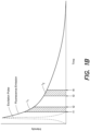
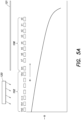
- FIG. 1A plots the probability of a photon being emitted as a function of time for two markers with different lifetimes.
- the marker represented by probability curve B has a probability of emission that decays more quickly than the probability of emission for the marker represented by probability curve A.
- the marker represented by probability curve B has a shorter temporal parameter, ⁇ , or lifetime than the marker represented by probability curve A.
- Markers may have fluorescence lifetimes ranging from 0.1-20 ns, in some embodiments. However, the techniques described herein are not limited as to the lifetimes of the marker(s) used.
- the lifetime of a marker may be used to distinguish among more than one marker, and/or may be used to identify marker(s).
- fluorescence lifetime measurements may be performed in which a plurality of markers having different lifetimes are excited by an excitation source.
- four markers having lifetimes of 0.5, 1, 2, and 3 nanoseconds, respectively, may be excited by a light source that emits light having a selected wavelength (e.g., 635nm, by way of example).
- the markers may be identified or differentiated from each other based on measuring the lifetime of the light emitted by the markers.
- Fluorescence lifetime measurements may use relative intensity measurements by comparing how intensity changes over time, as opposed to absolute intensity values. As a result, fluorescence lifetime measurements may avoid some of the difficulties of absolute intensity measurements. Absolute intensity measurements may depend on the concentration of fluorophores present and calibration steps may be needed for varying fluorophore concentrations. By contrast, fluorescence lifetime measurements may be insensitive to the concentration of fluorophores.
- Luminescent markers may be exogenous or endogenous.
- Exogenous markers may be external luminescent markers used as a reporter and/or tag for luminescent labeling.
- exogenous markers may include fluorescent molecules, fluorophores, fluorescent dyes, fluorescent stains, organic dyes, fluorescent proteins, enzymes, and/or quantum dots.
- exogenous markers may be conjugated to a probe or functional group (e.g., molecule, ion, and/or ligand) that specifically binds to a particular target or component. Attaching an exogenous tag or reporter to a probe allows identification of the target through detection of the presence of the exogenous tag or reporter.
- probes may include proteins, nucleic acids such as DNA molecules or RNA molecules, lipids and antibody probes.
- an exogenous marker and a functional group may form any suitable probes, tags, and/or labels used for detection, including molecular probes, labeled probes, hybridization probes, antibody probes, protein probes (e.g., biotin-binding probes), enzyme labels, fluorescent probes, fluorescent tags, and/or enzyme reporters.
- exogenous markers may be added to a sample or region
- endogenous markers may be already part of the sample or region.
- Endogenous markers may include any luminescent marker present that may luminesce or "autofluoresce” in the presence of excitation energy. Autofluorescence of endogenous fluorophores may provide for label-free and noninvasive labeling without requiring the introduction of endogenous fluorophores.
- endogenous fluorophores may include hemoglobin, oxyhemoglobin, lipids, collagen and elastin crosslinks, reduced nicotinamide adenine dinucleotide (NADH), oxidized flavins (FAD and FMN), lipofuscin, keratin, and/or prophyrins, by way of example and not limitation.
- NADH reduced nicotinamide adenine dinucleotide
- FAD and FMN oxidized flavins
- lipofuscin keratin, and/or prophyrins
- Differentiating between markers by lifetime measurements may allow for fewer wavelengths of excitation light to be used than when the markers are differentiated by measurements of emission spectra.
- sensors, filters, and/or diffractive optics may be reduced in number or eliminated when using fewer wavelengths of excitation light and/or luminescent light.
- labeling may be performed with markers that have different lifetimes, and the markers may be excited by light having the same excitation wavelength or spectrum.
- an excitation light source may be used that emits light of a single wavelength or spectrum, which may reduce the cost.
- the techniques described herein are not limited in this respect, as any number of excitation light wavelengths or spectra may be used.
- an integrated photodetector may be used to determine both spectral and temporal information regarding received light.
- a quantitative analysis of the types of molecule(s) present may be performed by determining a temporal parameter, a spectral parameter, or a combination of the temporal and spectral parameters of the emitted luminescence from a marker.
- An integrated photodetector that detects the arrival time of incident photons may reduce additional optical filtering (e.g., optical spectral filtering) requirements.
- an integrated photodetector according to the present application may include a drain to remove photogenerated carriers at particular times. By removing photogenerated carriers in this manner, unwanted charge carriers produced in response to an excitation light pulse may be discarded without the need for optical filtering to prevent reception of light from the excitation pulse.
- Such a photodetector may reduce overall design integration complexity, optical and/or filtering components, and/or cost.
- a fluorescence lifetime may be determined by measuring the time profile of the emitted luminescence by aggregating collected charge carriers in one or more time bins of the integrated photodetector to detect luminance intensity values as a function of time.
- the lifetime of a marker may be determined by performing multiple measurements where the marker is excited into an excited state and then the time when a photon emits is measured. For each measurement, the excitation source may generate a pulse of excitation light directed to the marker, and the time between the excitation pulse and subsequent photon event from the marker may be determined.
- the time between when a photon emission event occurs and the subsequent excitation pulse may be measured, and the measured time may be subtracted from the time interval between excitation pulses (i.e., the period of the excitation pulse waveform) to determine the time of the photon absorption event.
- the number of instances a photon is emitted from the marker within a certain time interval after excitation may be determined, which is indicative of the probability of a photon being emitted within such a time interval after excitation.
- the number of photon emission events collected may be based on the number of excitation pulses emitted to the marker.
- the number of photon emission events over a measurement period may range from 50-10,000,000 or more, in some embodiments, however, the techniques described herein are not limited in this respect.
- the number of instances a photon is emitted from the marker within a certain time interval after excitation may populate a histogram representing the number of photon emission events that occur within a series of discrete time intervals or time bins.
- the number of time bins and/or the time interval of each bin may be set and/or adjusted to identify a particular lifetime and/or a particular marker.
- the number of time bins and/or the time interval of each bin may depend on the sensor used to detect the photons emitted.
- the number of time bins may be 1, 2, 3, 4, 5, 6, 7, 8, or more, such as 16, 32, 64, or more.
- a curve fitting algorithm may be used to fit a curve to the recorded histogram, resulting in a function representing the probability of a photon to be emitted after excitation of the marker at a given time.
- a lifetime may be calculated from the intensity values at two time intervals.
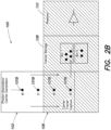
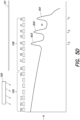
- FIG. 1B shows example intensity profiles over time for an example excitation pulse (dotted line) and example fluorescence emission (solid line).
- the photodetector measures the intensity over at least two time bins. The photons that emit luminescence energy between times t1 and t2 are measured by the photodetector as intensity I1 and luminescence energy emitted between times t3 and t4 are measured as I2. Any suitable number of intensity values may be obtained although only two are shown in FIG. 1B . Such intensity measurements may then be used to calculate a lifetime.
- the time binned luminescence signal may be fit to a single exponential decay. In some embodiments, only two time bins may be needed to accurately identify the lifetime for a fluorophore. When two or more fluorophores are present, then individual lifetimes may be identified from a combined luminescence signal by fitting the luminescence signal to multiple exponential decays, such as double or triple exponentials. In some embodiments two or more time bins may be needed in order to accurately identify more than one fluorescence lifetime from such a luminescence signal. However, in some instances with multiple fluorophores, an average fluorescence lifetime may be determined by fitting a single exponential decay to the luminescence signal.
- the probability of a photon emission event and thus the lifetime of a marker may change based on the surroundings and/or conditions of the marker. For example, the lifetime of a marker confined in a volume with a diameter less than the wavelength of the excitation light may be smaller than when the marker is not in the volume. Lifetime measurements with known markers under conditions similar to when the markers are used for labeling may be performed. The lifetimes determined from such measurements with known markers may be used when identifying a marker.
- Individual pixels on an integrated photodetector may be capable of fluorescence lifetime measurements used to identify fluorescent tags and/or reporters that label one or more targets, such as molecules or specific locations on molecules. Any one or more molecules of interest may be labeled with a fluorophore, including proteins, amino acids, enzymes, lipids, nucleotides, DNA, and RNA. When combined with detecting spectra of the emitted light or other labeling techniques, fluorescence lifetime may increase the total number of fluorescent tags and/or reporters that can be used.
- Identification based on lifetime may be used for single molecule analytical methods to provide information about characteristics of molecular interactions in complex mixtures where such information would be lost in ensemble averaging and may include protein-protein interactions, enzymatic activity, molecular dynamics, and/or diffusion on membranes. Additionally, fluorophores with different fluorescence lifetimes may be used to tag target components in various assay methods that are based on presence of a labeled component. In some embodiments, components may be separated, such as by using microfluidic systems, based on detecting particular lifetimes of fluorophores.
- Fluorescence lifetimes may be used in combination with other analytical methods.
- fluorescence lifetimes may be used in combination with fluorescence resonance energy transfer (FRET) techniques to discriminate between the states and/or environments of donor and acceptor fluorophores located on one or more molecules.
- FRET fluorescence resonance energy transfer
- Such measurements may be used to determine the distance between the donor and the acceptor.
- energy transfer from the donor to the acceptor may decrease the lifetime of the donor.
- fluorescence lifetime measurements may be used in combination with DNA sequencing techniques where four fluorophores having different lifetimes may be used to label the four different nucleotides (A, T, G, C) in a DNA molecule with an unknown sequence of nucleotides.
- the fluorescence lifetimes, instead of emission spectra, of the fluorophores may be used to identify the sequence of nucleotides.
- accuracy and measurement resolution may increase because artifacts due to absolute intensity measurements are reduced.
- lifetime measurements may reduce the complexity and/or expense of the system because fewer excitation energy wavelengths are required and/or fewer emission energy wavelengths need be detected.
- DNA sequencing allows for the determination of the order and position of nucleotides in a target nucleic acid molecule. Technologies used for DNA sequencing vary greatly in the methods used to determine the nucleic acid sequence as well as in the rate, read length, and incidence of errors in the sequencing process. A number of DNA sequencing methods are based on sequencing by synthesis, in which the identity of a nucleotide is determined as the nucleotide is incorporated into a newly synthesized strand of nucleic acid that is complementary to the target nucleic acid.
- Many sequencing by synthesis methods require the presence of a population of target nucleic acid molecules (e.g ., copies of a target nucleic acid) or a step of amplification of the target nucleic acid to achieve a population of target nucleic acids. Improved methods for determining the sequence of single nucleic acid molecules is desired.
- the target nucleic acid used in single molecule sequencing technology is a single stranded DNA template that is added to a sample well containing at least one component of the sequencing reaction (e.g ., the DNA polymerase) immobilized or attached to a solid support such as the bottom of the sample well.
- the sample well also contains deoxyribonucleoside triphosphates, also referred to a "dNTPs," including adenine, cytosine, guanine, and thymine dNTPs, that are conjugated to detection labels, such as fluorophores.
- each class of dNTPs are each conjugated to a distinct detection label such that detection of the signal indicates the identity of the dNTP that was incorporated into the newly synthesized nucleic acid.
- the detection label may be conjugated to the dNTP at any position such that the presence of the detection label does not inhibit the incorporation of the dNTP into the newly synthesized nucleic acid strand or the activity of the polymerase.
- the detection label is conjugated to the terminal phosphate (the gamma phosphate) of the dNTP.
- Any polymerase may be used for single molecule DNA sequencing that is capable of synthesizing a nucleic acid complementary to a target nucleic acid.
- polymerases include E . coli DNA polymerase I, T7 DNA polymerase, bacteriophage T4 DNA polymerase ⁇ 29 (psi29) DNA polymerase, and variants thereof.
- the polymerase is a single subunit polymerase.
- the polymerase Upon base pairing between a nucleobase of a target nucleic acid and the complementary dNTP, the polymerase incorporates the dNTP into the newly synthesized nucleic acid strand by forming a phosphodiester bond between the 3' hydroxyl end of the newly synthesized strand and the alpha phosphate of the dNTP.
- the detection label conjugated to the dNTP is a fluorophore
- its presence is signaled by excitation and a pulse of emission is detected during the step of incorporation.
- incorporation of the dNTP into the newly synthesized strand results in release the beta and gamma phosphates and the detection label, which is free to diffuse in the sample well, resulting in a decrease in emission detected from the fluorophore.
- an integrated photodetector may perform imaging to obtain spatial information regarding a region, object or scene and temporal information regarding the arrival of incident photons using the region, object or scene.
- the integrated photodetector may perform luminescence lifetime imaging of a region, object or sample, such as fluorescence lifetime imaging.
- the integrated photodetector described herein may be applied to the analysis of a plurality of biological and/or chemical samples, as discussed above, the integrated photodetector may be applied to other applications, such as imaging applications, for example.
- the integrated photodetector may include a pixel array that performs imaging of a region, object or scene, and may detect temporal characteristics of the light received at individual pixels from different regions of the region, object or scene.
- the integrated photodetector may perform imaging of tissue based on the temporal characteristics of light received from the tissue, which may enable a physician performing a procedure (e.g., surgery) to identify an abnormal or diseased region of tissue (e.g., cancerous or pre-cancerous).
- the integrated photodetector may be incorporated into a medical device, such as a surgical imaging tool.
- time-domain information regarding the light emitted by tissue in response to a light excitation pulse may be obtained to image and/or characterize the tissue. For example, imaging and/or characterization of tissue or other objects may be performed using fluorescence lifetime imaging.
- the integrated photodetector may be applied in a scientific or diagnostic context such as by performing imaging or analysis of biological and/or chemical samples, or imaging tissue, as described above, such an integrated photodetector may be used in any other suitable contexts.
- such an integrated photodetector may image a scene using temporal characteristics of the light detected in individual pixels.
- An example of an application for imaging a scene is range imaging or time-of-flight imaging, in which the amount of time light takes to reach the photodetector is analyzed to determine the distance traveled by the light to the photodetector.
- Such a technique may be used to perform three-dimensional imaging of a scene.
- a scene may be illuminated with a light pulse emitted from a known location relative to the integrated photodetector, and the reflected light detected by the photodetector.
- the amount of time that the light takes to reach the integrated photodetector at respective pixels of the array is measured to determine the distance(s) light traveled from respective portions of the scene to reach respective pixels of the photodetector.
- the integrated photodetector may be incorporated into a consumer electronic device such as a camera, cellular telephone, or tablet computer, for example, to enable such devices to capture and process images or video based on the range information obtained.
- the integrated photodetector described in the present application may be used to measure low light intensities.
- a photodetector may be suitable for applications that require photodetectors with a high sensitivity, such as applications that may currently use single photon counting techniques, for example.
- the techniques described herein are not limited in this respect, as the integrated photodetector described in the present applications may measure any suitable light intensities.
- a region, object or sample may be imaged and/or characterized using fluorescence lifetime imaging techniques though use of an integrated photodetector.
- the fluorescence characteristics of the region, object or sample itself may be used for imaging and/or characterization.
- Either exogenous markers or endogenous markers may be detected through lifetime imaging and/or characterization.
- Exogenous markers attached to a probe may be provided to the region, object, or sample in order to detect the presence and/or location of a particular target component.
- the exogenous marker may serve as a tag and/or reporter as part of a labeled probe to detect portions of the region, object, or sample that contains a target for the labeled probe.
- Autofluorescence of endogenous markers may provide a label-free and noninvasive contrast for spatial resolution that can be readily utilized for imaging without requiring the introduction of endogenous markers.
- autofluorescence signals from biological tissue may depend on and be indicative of the biochemical and structural composition of the tissue.
- Fluorescence lifetime measurements may provide a quantitative measure of the conditions surrounding the fluorophore.
- the quantitative measure of the conditions may be in addition to detection or contrast.
- the fluorescence lifetime for a fluorophore may depend on the surrounding environment for the fluorophore, such as pH or temperature, and a change in the value of the fluorescence lifetime may indicate a change in the environment surrounding the fluorophore.
- fluorescence lifetime imaging may map changes in local environments of a sample, such as in biological tissue (e.g., a tissue section or surgical resection). Fluorescence lifetime measurements of autofluorescence of endogenous fluorophores may be used to detect physical and metabolic changes in the tissue.
- changes in tissue architecture, morphology, oxygenation, pH, vascularity, cell structure and/or cell metabolic state may be detected by measuring autofluorescence from the sample and determining a lifetime from the measured autofluorescence.
- Such methods may be used in clinical applications, such as screening, image-guided biopsies or surgeries, and/or endoscopy.
- an integrated photodetector of the present application may be incorporated into a clinical tool, such as a surgical instrument, for example, to perform fluorescence lifetime imaging. Determining fluorescence lifetimes based on measured autofluorescence provides clinical value as a label-free imaging method that allows a clinician to quickly screen tissue and detect small cancers and/or pre-cancerous lesions that are not apparent to the naked eye.
- Fluorescence lifetime imaging may be used for detection and delineation of malignant cells or tissue, such as tumors or cancer cells which emit luminescence having a longer fluorescence lifetime than healthy tissue.
- fluorescence lifetime imaging may be used for detecting cancers on optically accessible tissue, such as gastrointestinal tract, bladder, skin, or tissue surface exposed during surgery.
- fluorescence lifetimes may be used for microscopy techniques to provide contrast between different types or states of samples.
- Fluorescence lifetime imaging microscopy FLIM
- FLIM Fluorescence lifetime imaging microscopy
- the pixel values in the image may be based on the fluorescence lifetime determined for each pixel in the photodetector collecting the field of view.
- an integrated photodetector as described in the present application may be used in scientific and clinical contexts in which the timing of light emitted may be used to detect, quantify, and or image a region, object or sample.
- the techniques described herein are not limited to scientific and clinical applications, as the integrated photodetector may be used in any imaging application that may take advantage of temporal information regarding the time of arrival of incident photons.
- An example of an application is time-of-flight imaging.
- an integrated photodetector may be used in imaging techniques that are based on measuring a time profile of scattered or reflected light, including time-of-flight measurements.
- a light pulse may be is emitted into a region or sample and scattered light may be detected by the integrated photodetector.
- the scattered or reflected light may have a distinct time profile that may indicate characteristics of the region or sample.
- Backscattered light by the sample may be detected and resolved by their time of flight in the sample.
- Such a time profile may be a temporal point spread function (TPSF).
- TPSF temporal point spread function
- the time profile may be acquired by measuring the integrated intensity over multiple time bins after the light pulse is emitted.
- Time-resolved diffuse optical imaging methods may include spectroscopic diffuse optical tomography where the light pulse may be infrared light in order to image at a further depth in the sample. Such time-resolved diffuse optical imaging methods may be used to detect tumors in an organism or in part of an organism, such as a person's head.
- time-of-flight measurements may be used to measure distance or a distance range based on the speed of light and time between an emitted light pulse and detecting light reflected from an object.
- time-of-flight techniques may be used in a variety of applications including cameras, proximity detection sensors in automobiles, human-machine interfaces, robotics and other applications that may use three-dimensional information collected by such techniques.
- Some embodiments relate to an integrated circuit having a photodetector that produces charge carriers in response to incident photons and which is capable of discriminating the timing at which the charge carriers are generated by the arrival of incident photons with respect to a reference time (e.g., a trigger event).
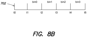
- a charge carrier segregation structure segregates charge carriers generated at different times and directs the charge carriers into one or more charge carrier storage regions (termed "bins") that aggregate charge carriers produced within different time periods. Each bin stores charge carriers produced within a selected time interval. Reading out the charge stored in each bin can provide information about the number of photons that arrived within each time interval.
- Such an integrated circuit can be used in any of a variety of applications, such as those described herein.
- the integrated circuit may include an array of pixels, and each pixel may include one or more photodetection regions and one or more charge carrier segregation structures, as discussed below.
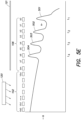
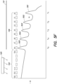
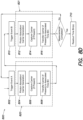
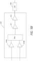
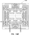
- FIG. 2A shows a diagram of a pixel 100, according to some embodiments.
- Pixel 100 includes a photon absorption/carrier generation region 102 (also referred to as a photodetection region), a carrier travel/capture region 106, a carrier storage region 108 having one or more charge carrier storage regions, also referred to herein as "charge carrier storage bins" or simply “bins,” and readout circuitry 110 for reading out signals from the charge carrier storage bins.
- the photon absorption/carrier generation region 102 may be a region of semiconductor material (e.g., silicon) that can convert incident photons into photogenerated charge carriers.
- the photon absorption/carrier generation region 102 may be exposed to light, and may receive incident photons. When a photon is absorbed by the photon absorption/carrier generation region 102 it may generate photogenerated charge carriers, such as an electron/hole pair. Photogenerated charge carriers are also referred to herein simply as "charge carriers.”
- An electric field may be established in the photon absorption/carrier generation region 102.
- the electric field may be "static," as distinguished from the changing electric field in the carrier travel/capture region 106.
- the electric field in the photon absorption/carrier generation region 102 may include a lateral component, a vertical component, or both a lateral and a vertical component.
- the lateral component of the electric field may be in the downward direction of FIG. 2A , as indicated by the arrows, which induces a force on photogenerated charge carriers that drives them toward the carrier travel/capture region 106.
- the electric field may be formed in a variety of ways.
- one or more electrodes may be formed over the photon absorption/carrier generation region 102.
- the electrodes(s) may have voltages applied thereto to establish an electric field in the photon absorption/carrier generation region 102.
- Such electrode(s) may be termed "photogate(s)."
- photon absorption/carrier generation region 102 may be a region of silicon that is fully depleted of charge carriers.
- the electric field in the photon absorption/carrier generation region 102 may be established by a junction, such as a PN junction.
- the semiconductor material of the photon absorption/carrier generation region 102 may be doped to form the PN junction with an orientation and/or shape that produces an electric field that induces a force on photogenerated charge carriers that drives them toward the carrier travel/capture region 106.
- Producing the electric field using a junction may improve the quantum efficiency with respect to use of electrodes overlying the photon absorption/carrier generation region 102 which may prevent a portion of incident photons from reaching the photon absorption/carrier generation region 102.
- Using a junction may reduce dark current with respect to use of photogates.
- the P terminal of the PN junction diode may connected to a terminal that sets its voltage.
- Such a diode may be referred to as a "pinned" photodiode.
- a pinned photodiode may promote carrier recombination at the surface, due to the terminal that sets its voltage and attracts carriers, which can reduce dark current.
- Photogenerated charge carriers that are desired to be captured may pass underneath the recombination area at the surface.
- the lateral electric field may be established using a graded doping concentration in the semiconductor material.
- a absorption/carrier generation region 102 that has a junction to produce an electric field may have one or more of the following characteristics:
- the electric field may be established in the photon absorption/carrier generation region 102 by a combination of a junction and at least one electrode.
- a junction and a single electrode, or two or more electrodes may be used.
- one or more electrodes may be positioned near carrier travel/capture region 106 to establish the potential gradient near carrier travel/capture region 106, which may be positioned relatively far from the junction.
- a photon may be captured and a charge carrier 101A (e.g., an electron) may be produced at time t1.
- a charge carrier 101A e.g., an electron
- an electrical potential gradient may be established along the photon absorption/ carrier generation region 102 and the carrier travel/capture region 106 that causes the charge carrier 101A to travel in the downward direction of FIG. 2A (as illustrated by the arrows shown in FIG. 2A ).
- the charge carrier 101A may move from its position at time t1 to a second position at time t2, a third position at time t3, a fourth position at time t4, and a fifth position at time t5.
- the charge carrier 101A thus moves into the carrier travel/capture region 106 in response to the potential gradient.
- the carrier travel/capture region 106 may be a semiconductor region.
- the carrier travel/capture region 106 may be a semiconductor region of the same material as photon absorption/carrier generation region 102 (e.g., silicon) with the exception that carrier travel/capture region 106 may be shielded from incident light (e.g., by an overlying opaque material, such as a metal layer).
- a potential gradient may be established in the photon absorption/carrier generation region 102 and the carrier travel/capture region 106 by electrodes positioned above these regions.
- An example of the positioning of electrodes will be discussed with reference to FIG. 3B .
- the techniques described herein are not limited as to particular positions of electrodes used for producing an electric potential gradient.
- an electric potential gradient may be established using a spatially graded doping profile and/or a PN junction. Any suitable technique may be used for establishing an electric potential gradient that causes charge carriers to travel along the photon absorption/carrier generation region 102 and carrier travel/capture region 106.
- a charge carrier segregation structure may be formed in the pixel to enable segregating charge carriers produced at different times.
- at least a portion of the charge carrier segregation structure may be formed over the carrier travel/capture region 106.
- the charge carrier segregation structure may include one or more electrodes formed over the carrier travel/capture region 106, the voltage of which may be controlled by control circuitry to change the electric potential in the carrier travel/capture region 106.
- the electric potential in the carrier travel/capture region 106 may be changed to enable capturing a charge carrier.
- the potential gradient may be changed by changing the voltage on one or more electrodes overlying the carrier travel/capture region 106 to produce a potential barrier that can confine a carrier within a predetermined spatial region.
- the voltage on an electrode overlying the dashed line in the carrier travel/capture region 106 of FIG. 2A may be changed at time t5 to raise a potential barrier along the dashed line in the carrier travel/capture region 106 of FIG. 2A , thereby capturing charge carrier 101A.
- the carrier captured at time t5 may be transferred to a bin "bin0" of carrier storage region 108.
- the transfer of the carrier to the charge carrier storage bin may be performed by changing the potential in the carrier travel/capture region 106 and/or carrier storage region 108 (e.g., by changing the voltage of electrode(s) overlying these regions) to cause the carrier to travel into the charge carrier storage bin.
- Changing the potential at a certain point in time within a predetermined spatial region of the carrier travel/capture region 106 may enable trapping a carrier that was generated by photon absorption that occurred within a specific time interval. By trapping photogenerated charge carriers at different times and/or locations, the times at which the charge carriers were generated by photon absorption may be discriminated. In this sense, a charge carrier may be "time binned" by trapping the charge carrier at a certain point in time and/or space after the occurrence of a trigger event.
- the time binning of a charge carrier within a particular bin provides information about the time at which the photogenerated charge carrier was generated by absorption of an incident photon, and thus likewise "time bins,” with respect to the trigger event, the arrival of the incident photon that produced the photogenerated charge carrier.
- FIG. 2B illustrates capturing a charge carrier at a different point in time and space.
- the voltage on an electrode overlying the dashed line in the carrier travel/capture region 106 may be changed at time t9 to raise a potential barrier along the dashed line in the carrier travel/capture region 106 of FIG. 2B , thereby capturing carrier 101B.
- the carrier captured at time t9 may be transferred to a bin "bin1" of carrier storage region 108.
- charge carrier 101B Since charge carrier 101B is trapped at time t9, it represents a photon absorption event that occurred at a different time (i.e., time t6) than the photon absorption event (i.e., at t1) for carrier 101A, which is captured at time t5.
- Performing multiple measurements and aggregating charge carriers in the charge carrier storage bins of carrier storage region 108 based on the times at which the charge carriers are captured can provide information about the times at which photons are captured in the photon absorption/carrier generation area 102. Such information can be useful in a variety of applications, as discussed above.
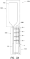
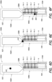
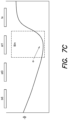
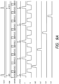
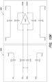
- FIG. 3A shows a charge carrier confinement region 103 of a pixel 100A, according to some embodiments.
- pixel 100A may include a photon absorption/carrier generation area 102A (also referred to as a photodetection region), a carrier travel/capture area 106A, a drain 104, a plurality of charge carrier storage bins bin0, bin1, bin2, and bin3 of a carrier storage region 108A, and a readout region 110A.
- Charge carrier confinement region 103 is a region in which photogenerated charge carriers move in response to the electric potential gradient produced by a charge carrier segregation structure. Charge carriers may be generated in photon absorption/carrier generation area 102A within charge carrier confinement region 103.
- Charge carrier confinement region 103 may be formed of any suitable material, such as a semiconductor material (e.g., silicon). However, the techniques described herein are not limited in this respect, as any suitable material may form charge carrier confinement region 103. In some embodiments, charge carrier confinement region 103 may be surrounded by an insulator (e.g., silicon oxide) to confine charge carriers within charge carrier confinement region 103.
- a semiconductor material e.g., silicon
- an insulator e.g., silicon oxide
- the portion of charge carrier confinement region 103 in photon absorption/carrier generation area 102A may have any suitable shape. As shown in FIG. 3A , in some embodiments the portion of charge carrier confinement region 103 in photon absorption/carrier generation area 102A may have a tapered shape, such that its width gradually decreases near carrier travel/capture area 106A. Such a shape may improve the efficiency of charge handling, which may be useful particularly in cases where few photons are expected to arrive. In some embodiments the portion of charge carrier confinement region 103 in photon absorption/carrier generation area 102A may be less tapered, or may not be tapered, which can increase the dynamic range. However, the techniques described herein are not limited as to the shape of charge carrier confinement region 103 in photon absorption/carrier generation area 102A.
- a first portion of charge carrier confinement region 103 in carrier travel/capture area 106A may extend from the photon absorption/carrier generation area 102A to a drain 104. Extensions of the charge carrier confinement region 103 extend to the respective charge storage bins, allowing charge carriers to be directed into the charge carrier storage bins by a charge carrier segregation structure such as that described with respect to FIG. 3B . In some embodiments, the number of extensions of the charge carrier confinement region 103 that are present may be the same as the number of charge carrier storage bins, with each extension extending to a respective charge carrier storage bin.
- Readout region 110A may include a floating diffusion node fd for read out of the charge storage bins.
- Floating diffusion node fd may be formed by a diffusion of n-type dopants into a p-type material (e.g., a p-type substrate), for example.
- a p-type material e.g., a p-type substrate
- the techniques described herein are not limited as to particular dopant types or doping techniques.
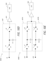
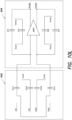
- FIG. 3B shows the pixel 100A of FIG. 3A with a plurality of electrodes Vb0-Vbn, b0-bm, st1, st2, and tx0-tx3 overlying the charge carrier confinement region 103 of FIG. 3A .
- the electrodes shown in FIG. 3B form at least a portion of a charge carrier segregation structure that can time-bin photogenerated carriers.
- the electrodes shown in FIG. 3B establish an electric potential within the charge carrier confinement region 103.
- the electrodes Vb0-Vbn, b0-bm may have a voltage applied thereto to establish a potential gradient within regions 102A and 106A such that charge carriers, e.g., electrons, travel in the downward direction of FIG. 3B toward the drain 104.
- Electrodes Vb0-Vbn may establish a potential gradient in the charge confinement region 103 of photon absorption/carrier generation area 102A.
- respective electrodes Vb0-Vbn may be at constant voltages.
- Electrodes b0-bm may establish a potential gradient in the charge confinement region 103 of carrier travel/capture area 106A.
- electrodes b0-bm may have their voltages set to different levels to enable trapping charge carriers and/or transferring charge carriers to one or more charge storage bins.
- Electrodes st0 and st1 may have voltages that change to transfer carriers to the charge storage bins of charge carrier storage region 108A. Transfer gates tx0, tx1, tx2 and tx3 enable transfer of charge from the charge storage bins to the floating diffusion node fd. Readout circuitry 110 including reset transistor rt, amplification transistor sf and selection transistor rs is also shown.
- the potentials of floating diffusion node fd and each of the transfer gates tx0-tx3 may allow for overflow of charge carriers into the floating diffusion rather than into the carrier travel/capture area 106A.
- the potentials of the floating diffusion node fd and the transfer gates tx0-tx3 may be sufficiently high to allow any overflow charge carriers in the bin to flow to the floating diffusion.
- Such a "barrier overflow protection" technique may reduce carriers overflowing and diffusing into the carrier travel/capture area 106A and/or other areas of the pixel.
- a barrier overflow protection technique may be used to remove any overflow charge carriers generated by an excitation pulse. By allowing overflow charge carriers to flow to the floating diffusion, these charge carriers are not captured in one or more time bins, thereby reducing the impact of the excitation pulse on the time bin signals during readout.
- the electrodes Vb0-Vbn and b0-bm may be set to voltages that increase for positions progressing from the top to the bottom of FIG. 3B , thereby establishing the potential gradient that causes charge carriers to travel in the downward direction of FIG. 3B toward the drain 104.
- the potential gradient may vary monotonically in the photon absorption/carrier generation region 102 and/or the carrier travel/capture region 106, which may enable charge carriers to travel along the potential gradient into the carrier travel/ capture region 106.
- the potential gradient may change linearly with respect to position along the line A-A'.
- a linear potential gradient may be established by setting electrodes to voltages that vary linearly across the vertical dimension of FIG. 3B .
- the techniques described herein are not limited to a linear potential gradient, as any suitable potential gradient may be used.
- the electric field in the carrier travel/capture region 106 may be high enough so charge carriers move fast enough in the carrier travel/capture region 106 such that the transit time is small compared to the time over which photons may arrive.
- the transit time of charge carriers may be made small compared to the lifetime of a luminescent marker being measured. The transit time can be decreased by producing a sufficiently graded electric field in the carrier travel/capture region 106.
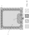
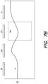
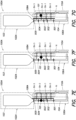
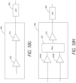
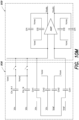
- FIG. 3C shows an embodiment in which the photon absorption/carrier generation region 102 includes a PN junction.
- FIG. 3C shows an outer electrode 302, which may be at a relatively low potential, thereby "pinning" the surface potential at a relatively low potential.
- An electrode 304 may be included to assist in producing the potential gradient for a static electric field that drives carriers toward carrier travel/capture area 106 (the lower portion of carrier travel/capture area 106 is not shown).
- FIG. 3C indicates regions of diffusion, polysilicon, contact and metal 1.
- FIG. 3D shows a top view of a pixel as in FIG. 3C , with the addition of doping characteristics.
- FIG. 3D also shows the electric field sweeping carriers down to region 106 along the potential gradient established by the PN junction and the electrode 304.
- FIG. 3D indicates regions of diffusion, polysilicon, contact, metal 1, N-implant, P-implant, and P-epi.
- FIG. 3E shows a top view of a pixel as in FIG. 3C , including the carrier travel/capture area 106.
- FIG. 3F shows an array of pixels as in FIG. 3E .
- FIG. 3F indicates regions of diffusion, polysilicon, contact and metal 1.
- FIG. 3G shows the pixel array of FIG. 3F and also indicates regions of diffusion, polysilicon, contact, metal 1, N-implant, P-implant, and P-epi.
- FIG. 4 shows a circuit diagram of the pixel 100A of FIG. 3B .
- the charge carrier confinement area 103 is shown in heavy dark lines. Also shown are the electrodes, charge carrier storage area 108 and readout circuitry 110.
- the charge storage bins bin0, bin1, bin2, and bin3 of carrier storage region 108 are within the carrier confinement area 103 under electrode st1.
- a junction may be used to produce a static field in region 102 instead of or in addition to the electrodes.
- Light is received from a light source 120 at photon absorption/carrier generation area 102.
- Light source 120 may be any type of light source, including a luminescent sample (e.g., linked to a nucleic acid) or a region or scene to be imaged, by way of example and not limitation.
- a light shield 121 prevents light from reaching carrier travel/capture area 106.
- Light shield 121 may be formed of any suitable material, such a metal layer of the integrated circuit, by way of example and not limitation.
- FIG. 5A illustrates a potential gradient that may be established in the charge carrier confinement area 103 in photon absorption/carrier generation area 102 and carrier travel/capture area 106 along the line A-A' of FIG. 3B .
- a charge carrier e.g., an electron
- Electrodes Vb0-Vbn and b0-bm are set to voltages that increase to the right of FIG. 5A to establish the potential gradient the causes electrons to flow to the right in FIG. 5A (the downward direction of FIG. 3B ).
- a PN junction may be present to establish or assist in establishing the field.
- FIG. 5A shows the potential in the region where the carriers flow.
- carriers may be allowed to flow through the carrier travel/capture area 106 into the drain 104, as shown in FIGS. 6A, 6B and 6C.
- FIG. 6A shows the position of a carrier 101 once it is photogenerated.
- FIG. 6B shows the position of a carrier 101 shortly thereafter, as it travels in the downward direction in response to the established potential gradient.
- FIG. 6C shows the position of the carrier 101 as it reaches the drain 104.
- FIG. 5B shows that after a period of time a potential barrier 501 to electrons is raised at a time t1 by decreasing the voltage of electrode b0.
- the potential barrier 501 may stop an electron from traveling to the right in FIG. 5B , as shown in FIG. 6D, 6E and 6F.
- FIG. 6D shows the position of a carrier 101 (e.g., an electron) once it is photogenerated.
- FIG. 6E shows the position of a carrier 101 shortly thereafter, as it travels in the downward direction in response to the potential gradient.
- FIG. 6F shows the position of the carrier 101 as it reaches the potential barrier 501 after time t1.
- FIG. 5C shows that after another time period, another potential barrier 502 to electrons is raised at time t2 by decreasing the voltage of electrode b2. If an electron arrives between electrodes b0 and b2 between times t1 and t2, the electron will be captured between potential barrier 501 and potential barrier 502, as illustrated in FIG. 5C and FIG. 6G .
- FIG. 5D shows that after another time period, another potential barrier 503 to electrons may be raised at time t3 by decreasing the voltage of electrode b4. If an electron arrives between electrodes b2 and b4 between times t2 and t3, the electron will be trapped in a location between potential barrier 502 and potential barrier 503. In the example of FIG. 5D and 6H , an electron arrived between times t1 and t2, so it remains captured between potential barrier 501 and potential barrier 502.
- FIG. 5E shows that after another time period, another potential barrier 504 to electrons may be raised at time t4 by decreasing the voltage of electrode b6. If an electron arrives between electrodes b4 and b6 between times t3 and t4, the electron will be trapped in a location between potential barrier 503 and potential barrier 504. In the example of FIG. 5E and 6I , an electron arrived between times t1 and t2, so it remains captured between potential barrier 501 and potential barrier 502.
- FIG. 5F shows that after another time period, another potential barrier 505 to electrons may be raised at time t5 by decreasing the voltage of electrode bm. If an electron arrives between electrodes b6 and bm between times t4 and t5, the electron will be trapped in a location between potential barrier 504 and potential barrier 505. In the example of FIG. 5F and 6J , an electron arrived between times t1 and t2, so it remains captured between potential barrier 501 and potential barrier 502.
- FIG. 6K shows a voltage timing diagram illustrating the voltages of electrodes b0-b8, st0 and st1 over time.
- a charge carrier moving through the carrier travel/capture area 106 during the sequence of raising potential barriers 501-505 will be captured at a location within the carrier travel/capture area 106 that depends on the time at which it arrives at the carrier travel/capture area 106, which in turn depends upon the time at which the charge carrier was generated by photon absorption in photon absorption/carrier generation area 102.
- the timing with which potential barriers 501-505 are raised sets the timing of the charge storage bins bin0-bin3. As shown in FIG.
- a carrier that arrives between times t1 and t2 will be trapped within a time interval for bin0
- a carrier that arrives between times t2 and t3 will be trapped within a time interval for bin1
- a carrier that arrives between times t3 and t4 will be trapped within a time interval for bin2
- a carrier that arrives between times t4 and t5 will be trapped within a time interval for bin3.
- a captured charge carrier may then be transferred to the appropriate charge carrier storage bin based on the location at which the charge carrier is captured within the carrier travel/capture area 106.
- a captured charge carrier may then be transferred to the appropriate charge carrier storage bin based on the location at which the charge carrier is captured within the carrier travel/capture area 106.
- it is transferred to bin0.
- an electron is captured under electrode b3, it is transferred to bin1.
- an electron is captured under electrode b5, it is transferred to bin2.
- transfer of any captured carrier(s) within the carrier travel/capture area 106 to their corresponding bin(s) may be performed in parallel (e.g., simultaneously).
- the techniques described herein are not limited as to transferring captured carriers to charge storage bins in parallel.
- the voltages on electrodes st0 and st1 may be changed to transfer any captured charge carriers to the corresponding charge carrier storage bin(s).
- An example sequence for transferring captured charge carrier(s) will be discussed with respect to FIG. 6K and FIGS. 7A-7G .
- FIG. 7A shows a plot of the of potential for a cross section of the charge carrier confinement area 103 along the line B-B' of FIG. 3B .
- FIG. 7A shows the potential at time t5 ( FIG. 6K ) in an example where an electron is captured between potential barriers 503 and 504.
- FIG. 7E A plan view showing an electron captured between potential barriers 503 and 504 is shown in FIG. 7E .
- FIG. 7B shows that after time t5 the voltage on electrodes b1, b3, b5 and b7 optionally may be decreased (not shown in FIG. 6K ) to raise the position of an electron within the potential well, to facilitate transferring the electron.
- FIG. 7C shows that at time t6 ( FIG. 6K ), the voltages on electrodes st0 and st1 may be raised. Changing the voltages of the electrodes in this manner may provide a potential gradient that causes a transfer a charge carrier captured in carrier travel/capture area 106 to a corresponding charge storage bin under electrode st1.
- a plan view showing the voltage of electrode st1 being raised and the carrier 101 being transferred is shown in FIG. 7F .
- FIG. 7D shows that at time t7, the voltage on electrode st0 may be dropped, thereby confining the captured carrier (if any) in the corresponding bin (bin2 in this example).
- the voltage on electrode b6 may be raised at time t8 to reestablish the potential gradient in the carrier travel/capture area 106.
- a plan view showing the voltage electrode st1 being lowered and the carrier 101 being captured in bin2 is shown in FIG. 7G .
- FIG. 7H shows the characteristics of the electrodes of a charge carrier segregation structure, according to some embodiments.
- FIG. 7H specifies, for each electrode, the voltage during the gradient phase, the voltage during the binning phase, the voltage during the transfer phase, the voltage during the readout phase the high, and type of voltage change.
- this is merely an example, and the techniques described herein are not limited as to the implementation details illustrated in FIG. 7H .
- Repeating the process of photon absorption / carrier generation and time binning of photogenerated charge carriers may enable gathering statistical information about the times at which photons arrive at the photodetector, as discussed below.
- a "measurement” may include receiving a photon, capturing a charge carrier at a particular time and/or location and transferring the captured carrier to a charge storage node corresponding to a particular time period or bin.
- a measurement may be repeated a plurality of times to gather statistical information about the times at which photons arrive at the photodetector.
- FIG. 8A shows a flowchart of a method 700 that includes performing a plurality of measurements 720, according to some embodiments. Such a method may be performed at least partially by an integrated device as described herein.
- a measurement 720 may be initiated by a trigger event.
- a trigger event may be an event that serves as a time reference for time binning arrival of a photon.
- the trigger event could be an optical pulse or an electrical pulse, for example, and could be a singular event or a repeating, periodic event.
- the trigger event may be the generation of a light excitation pulse to excite a fluorophore.
- the trigger event may be a pulse of light (e.g., from a flash) emitted by an imaging device comprising the integrated photodetector.
- the trigger event can be any event used as a reference for timing the arrival of photons or carriers.
- the generation of the light excitation pulse may produce a significant number of photons, some of which may reach the pixel 100 and may produce charge carriers in the photon absorption/carrier generation area 102. Since photogenerated carriers from the light excitation pulse are not desired to be measured, they may be allowed to flow down the electric potential to the drain 104 without being captured. Allowing photogenerated carriers produced by a light excitation pulse to flow to the drain 104 without being captured may reduce the amount of unwanted signal that otherwise may need to be prevented from arriving by complex optical components, such as a shutter or filter, which may add additional design complexity and/or cost.
- the timing of the raising of one or more potential barriers within the carrier travel/capture area 106 may be timed such that photogenerated carriers caused by any unwanted optical signal flow to the drain 104.
- a pixel may include a single time bin and a drain where the timing of the potential barriers reduces signal associated with the excitation pulse while capturing the desired optical signal within the carrier travel/capture area 106.
- the measurement 720 may then commence at step 704, in which photon(s) desired to be detected may be absorbed and a charge carrier may be generated in region 102.
- step 704 may commence after the light excitation pulse is completed.
- charge carrier(s) moving through the carrier travel/capture area 106 may be captured at predetermined locations at selected times with respect to trigger event 702.
- charge carrier(s) may be captured in one or more regions of the carrier travel/capture area 106 by raising one or more potential barriers to trap a carrier in a location that depends upon the time at which it was generated by photon absorption, as discussed above.
- captured charge carrier(s), if present, may be transferred from the location at which captured charge carrier(s) were captured to a corresponding charge storage bin, thereby "time-binning" the charge carrier.
- the measurement 720 may be repeated n-1 times to obtain statistical information regarding the time periods at which photons tend to arrive after a trigger event 702.
- Time-binned charge carriers may be aggregated in the corresponding charge storage bins as the measurement 720 is repeated. Repeating the measurement 720 may enable aggregating a sufficient number of charge carriers in the charge carrier storage bins to provide statistically meaningful results. For example, in the context of fluorescence lifetime measurement, it may be expected that a photon absorption event in response to a photon received from a fluorophore may occur relatively rarely. For example, such an event may be expected to occur once in about 1,000 measurements.
- a large number of measurements 720 may need to be performed to aggregate a sufficient number of charge carriers in the charge carrier storage bins such that the results are statistically meaningful.
- the number of measurements n of a fluorophore that may be performed for fluorescence lifetime measurement may be 500,000 or more, or 1,000,000 or more, to enable capturing and binning a sufficient number of charge carriers in each bin (i.e., tens or hundreds, or more, in some embodiments).
- Reading out the time bins may include converting the amount of charge aggregated in each of the charge storage bins into corresponding voltages, as will be discussed below.
- FIG. 8B is a diagram showing an excitation pulse being generated at time t0, and time bins bin0-bin3. Note that in this example the time bins for measuring photons do not begin until t1, a period of time after t0, which lets the excitation light end prior to measuring signal photons.
- FIG. 8C shows a plot of the number of photons / charge carriers in each time bin for a set of fluorescence lifetime measurements in which the probability of a marker or die fluorescing decreases exponentially over time.
- Method 700 may be performed over any suitable time period in which photons are desired to be captured.
- a suitable period for performing method 700 may be 10 milliseconds, for example.
- steps 702 to 708 may be repeated at a frequency that is the MHz range.
- the time bins may have a resolution on the scale of picoseconds or nanoseconds.
- measurements may be performed using a plurality of different types of trigger events.
- the trigger events may be multiplexed in time such that a pixel receives light in response to different types trigger events in different time periods.
- the trigger events may be excitation light pulses (e.g., laser pulses) of different wavelengths ⁇ 1 and ⁇ 2 , which can excite different luminescent molecules (e.g., fluorophores).
- fluorophores may be identified and/or discriminated from one another based on their response to different wavelengths ⁇ 1 and ⁇ 2 of excitation light.
- Exciting a sample with light excitation pulses of wavelengths ⁇ 1 and ⁇ 2 at different times, and analyzing the luminance emitted by the sample in response, can enable detecting and/or identifying luminescent molecules based on whether luminescence is detected in a first time period in response to excitation light of wavelength ⁇ 1 , or in a second time period in response to excitation light of wavelength ⁇ 2 .
- luminescent molecules may be identified and/or discriminated based upon measuring their luminance lifetimes.
- a nucleic acid may be sequenced based upon detecting light emitted by one or more fluorophores attached to nucleotides of the nucleic acid. In some embodiments, such sequencing may be performed by temporal multiplexing of excitation light of different wavelengths, based upon measuring luminance lifetimes, or based upon a combination of such techniques.
- four different fluorophores may be linked to respective nucleotides (e.g., A, C, G and T) of a nucleic acid.
- the four fluorophores may be distinguishable from one another based upon a combination of excitation wavelength and luminance lifetime, as illustrated in the chart below.
- the integrated photodetector may temporally multiplex detection of photons produced by a sample in response to light excitation pulses of different wavelengths. For example, in a first time period, light produced by a sample in response to excitation light of wavelength ⁇ 1 may be detected. Subsequently, in a second time period, light produced by a sample in response to excitation light of wavelength ⁇ 2 may be detected. To do so, a pixel having a plurality of time bins may use a first subset of time bins to detect arrival of photons in the first time period and a second subset of time bins to detect arrival of photons in the second time period. By examining whether light arrives at a pixel during the first time period or the second time period, it can be determined whether a fluorophore is fluorescing in response to light of wavelength ⁇ 1 or light of wavelength ⁇ 2 .
- information regarding the arrival times of photons in response to a light excitation pulse can be used to determine and/or discriminate fluorescence lifetime, and thereby identify a fluorophore.
- a first excitation pulse of a first wavelength may be emitted, then a first subset of the time bins of a pixel may be used to time-bin the arrival of incident photons in a first time interval.
- a second excitation pulse of a second wavelength may be emitted, and a second subset of time bins of the pixel may be used to time-bin the arrival of incident photons in a second time interval.
- the sequence of nucleotides in a nucleic acid can be determined.
- FIG. 8D shows a method of operating the integrated photodetector according to some embodiments in which light is received at the integrated photodetector in response to a plurality of different trigger events.
- FIG. 8E illustrates voltages of the electrodes of the charge carrier segregation structure when performing the method of FIG. 8D .
- a measurement 820 may be initiated by a trigger event A.
- Trigger event A may be an event that serves as a time reference for time binning arrival of a photon.
- the trigger event may be an optical pulse or an electrical pulse, for example, and could be a singular event or a repeating, periodic event.
- the trigger event A may be the generation of a light excitation pulse at a first wavelength to excite a first type of fluorophore.
- the generation of the light excitation pulse may produce a significant number of photons, some of which may reach the pixel 100 and may produce charge carriers in the photon absorption/carrier generation area 102. Since photogenerated carriers from the light excitation pulse are not desired to be measured, they may be allowed to flow down the electric potential to the drain 104 without being captured, as discussed above. The raising of one or more potential barriers within the carrier travel/capture area 106 may be timed such that photogenerated carriers caused by any unwanted optical signal flow to the drain 104.
- step 804 may commence after the light excitation pulse is completed.
- charge carrier(s) moving through the carrier travel/capture area 106 may be captured at predetermined locations at selected times with respect to trigger event 802.
- charge carrier(s) may be captured in one or more regions of the carrier travel/capture area 106 by raising one or more potential barriers to trap a carrier in a location that depends upon the time at which it was generated by photon absorption, as discussed above.
- step 806 may include raising potential barriers 501, 503 and 503 in succession, thereby capturing charge (if present) corresponding to time bins bin0 and/or bin1.
- captured charge carrier(s), if present, may be transferred from the location at which they were captured to a corresponding charge storage bin, thereby "time-binning" the charge carrier.
- any charge captured corresponding to time bins bin0 and/or bin1 may be transferred to bins bin0 and/or bin1 in step 808 using a technique shown in FIGS. 7A-7D , for example.
- a second measurement 821 may be initiated by a trigger event B.
- Trigger event B may be an event that serves as a time reference for time binning arrival of a photon.
- the trigger event may be an optical pulse or an electrical pulse, for example, and could be a singular event or a repeating, periodic event.
- the trigger event B may be the generation of a light excitation pulse at a second wavelength to excite a second type of fluorophore.
- the generation of the light excitation pulse may produce a significant number of photons, some of which may reach the pixel 100 and may produce charge carriers in the photon absorption/carrier generation area 102. Since photogenerated carriers from the light excitation pulse are not desired to be measured, they may be allowed to flow down the electric potential to the drain 104 without being captured, as discussed above. The raising of one or more potential barriers within the carrier travel/capture area 106 may be timed such that photogenerated carriers caused by any unwanted optical signal flow to the drain 104.
- the second measurement 821 may then proceed at step 812, in which photon(s) desired to be detected may be absorbed and a charge carrier may be generated in region 102.
- step 812 may commence after the second light excitation pulse is completed.
- charge carrier(s) moving through the carrier travel/capture area 106 may be captured at predetermined locations at selected times with respect to trigger event 810.
- charge carrier(s) may be captured in one or more regions of the carrier travel/capture area 106 by raising one or more potential barriers to trap a carrier in a location that depends upon the time at which it was generated by photon absorption, as discussed above.
- step 814 may include raising potential barriers 503, 504 and 505 in succession, thereby capturing charge (if present) corresponding to time bins bin2 and/or bin3.
- captured charge carrier(s), if present, may be transferred from the location at which they were captured to a corresponding charge storage bin, thereby "time-binning" the charge carrier.
- any charge captured corresponding to time bins bin2 and/or bin3 may be transferred to bins bin2 and/or bin3 in step 816 using a technique shown in FIGS. 7A-7D , for example.
- a pixel has four time bins, and two bins are allocated to measuring arrival times of light produced in response to each of the respective light excitation pulses
- the techniques described herein are not limited in this respect.
- the pixel may have a larger or smaller number of bins, which may be allocated in any suitable way to measuring light in response to different excitation pulses.
- the techniques described herein are not limited to light excitation pulses of two different wavelengths, as light excitation pulses of any number of wavelengths may be used, and multiplexed accordingly.
- the measurements 820 and 821 may be repeated n-1 times to obtain statistical information regarding the time periods at which photons tend to arrive after a trigger event.
- Time-binned charge carriers may be aggregated in the corresponding charge storage bins as the measurements are repeated.
- Reading out the time bins may include converting the amount of charge aggregated in each of the charge storage bins into corresponding voltages, as will be discussed below.
- pixel 100 may include readout circuitry 110 that allows reading out the charge stored in the charge storage bin(s) of the charge carrier storage region 108.
- Pixel 100 may be an active pixel, such that readout circuitry 110 includes a readout amplifier, or a passive pixel in which readout circuitry 110 does not include a readout amplifier. Any suitable type of active pixel or passive pixel readout circuitry may be used.
- readout circuitry 110 includes a readout amplifier
- any suitable type of amplifier may be used.
- suitable amplifiers include amplifiers abased on a common source configuration and amplifiers abased on a source-follower configuration.
- the techniques described herein are not limited as to any particular amplifier configuration.
- the readout amplifier may take the charge accumulated in a charge storage bin (e.g., bin0, bin1, bin2 or bin3) as an input and produce a voltage representative of the charge in the charge storage bin as an output.
- a charge storage bin e.g., bin0, bin1, bin2 or bin3
- FIG. 4 One example of readout circuitry 110 based on a source-follower configuration is illustrated in FIG. 4 .
- the example of readout circuitry 110 shown in FIG. 4 is a "4T" configuration having four transistors: rt, sf, rs, and one of the transfer gates tx0-tx3. Since the three transistors rt, sf, and rs are shared among each charge storage bin, the example circuitry shown in FIG. 4 for all four bins is a "1.75T" configuration, (4 transfer gates + 3 transistors)/4 bins.
- the techniques described herein are not limited to using readout circuitry 110 having a 1.75T configuration, as any other suitable type of readout configuration may be used.
- readout circuitry 110 may read out the charge carrier storage bins using correlated double sampling.
- Correlated double sampling is technique in which a first sample may be taken of a node at a reset voltage level which includes an undetermined amount of noise, and a second sample may be taken of a signal level at the node including the same undetermined noise. The noise can be subtracted out by subtracting the sampled reset level from the sampled signal level.
- Readout circuitry 110 may perform readout of the charge storage bins sequentially or in parallel.
- An example of a timing diagram for sequentially reading out bins bin0-bin3 with readout circuitry 110 shown in FIG. 4 using correlated double sampling is shown in FIG. 9A .
- initially reset transistor rt may be turned on to set the floating diffusion node fd to a reset voltage ct.
- the transfer gates tx0-tx3 are turned off to keep the charge carriers stored in their respective bins.
- the reset voltage may be sampled by turning off transistor rt and turning on transistor rs to produce an output voltage cb.
- the reset voltage represented by output voltage cb may be stored in an analog format (e.g., on a capacitor) or in a digital format (e.g., by A/D conversion and storage). Then, transfer gate tx0 may be turned on to allow the charge from bin0 to flow to the floating diffusion fd. The signal voltage may be sampled by turning on transistor rs to produce an output voltage cb based on the charge stored in bin0.
- the signal voltage represented by output voltage cb may be stored in an analog format (e.g., on a capacitor) or in a digital format (e.g., by A/D conversion and storage).
- transistor rt may be turned on to set the floating diffusion fd to a reset voltage ct.
- the transfer gates tx0-tx3 are turned off to keep the charge carriers stored in their respective bins.
- the reset voltage may be sampled by turning off transistor rt and turning on transistor rs to produce an output voltage cb.
- the reset voltage represented by output voltage cb may be stored in an analog format (e.g., on a capacitor) or in a digital format (e.g., by A/D conversion and storage).
- transfer gate tx1 may be turned on to allow the charge from bin1 to flow to the floating diffusion.
- the signal voltage may be sampled by turning on transistor rs to produce an output voltage cb based on the charge stored in bin1.
- the signal voltage represented by output voltage cb may be stored in an analog format (e.g., on a capacitor) or in a digital format (e.g., by A/D conversion and storage).
- the same process may then be performed for bin2 and bin3 by performing a reset, sampling the reset voltage, transferring the charge from a bin to the floating diffusion node fd, and sampling the signal. Accordingly, in the readout sequence illustrated in FIG. 9A , eight samples may be taken representing the reset value and signal values for the four bins. The stored reset value for each bin may be subtracted from the stored signal value to obtain a result indicative of the charge stored in each bin, thus completing the correlated double sampling process.
- the sampled reset voltage level for a bin may be stored on a first capacitor and the sampled signal for the bin may be stored on a second capacitor.
- the capacitors may be cleared by setting them to the same voltage.
- FIG. 9B shows a readout sequence for performing correlated double sampling that does not require measuring a reset value for each signal value, according to some embodiments.
- a single reset value is measured for all the bins of the pixel.
- a reset value may be subtracted from the measured signal value, as discussed above.
- charge may be transferred to the floating diffusion from the second bin, thereby aggregating the charge for the first and second bins.
- the signal for the second bin can be obtained by subtracting the signal for the first bin from the aggregated signal for the first and second bins.
- both the signal for the first bin and the aggregated signal for the first and second bins include the same reset noise, the result is that the reset noise is subtracted out.
- the process may continue for the remaining bins, with the aggregated signal for the previous bin being subtracted from the aggregated signal for the next bin. Aggregating the stored charge for the bins in this manner can allow reading our larger signals than would be the case if each bin were read out individually, and can reduce noise, as the sampled signals will be higher above the noise floor than would be the case if each bin were read out individually.
- five samples may be taken - one reset value and four samples representing the cumulative charge stored in the charge storage bins. This process will be described in greater detail with reference to FIG. 9B .
- initially reset transistor rt may be turned on to set the floating diffusion node fd to a reset voltage ct.
- the transfer gates tx0-tx3 are turned off to keep the charge carriers stored in their respective bins.
- the reset voltage may be sampled by turning off transistor rt and turning on transistor rs to produce an output voltage cb.
- the reset voltage represented by output voltage cb may be stored in an analog format (e.g., on a capacitor) or in a digital format (e.g., by A/D conversion and storage).
- transfer gate tx0 may be turned on to allow the charge from bin0 to flow to the floating diffusion.
- the signal voltage for bin0 may be sampled by turning on transistor rs to produce an output voltage cb based on the charge stored in bin0.
- transfer gate tx1 may be turned on to allow the charge from bin1 to flow to the floating diffusion.
- the signal voltage for bin1 + bin0 may be sampled by turning on transistor rs to produce an output voltage cb based on the charge stored in bin1 plus the charge stored on bin0.
- the output signal value for bin0 may be subtracted from the output signal value for bin0+bin1 to produce a signal indicative of the charge stored on bin1.
- a similar process may then be performed for bin2 and bin3 by subtracting the measured signal level for bin n from the measured signal level for bin n +1. Accordingly, using such a technique the number of samples that may need to be taken may be reduced.
- oversampling of the readout from a pixel may be performed. Oversampling involves reading the same signal from the pixel a plurality of times. Each time a signal is read from the pixel, there may be slight variations in the signal that is read due to noise. Oversampling of the readout of a signal and averaging the samples can reduce the noise (e.g., white noise) in measurements. In some embodiments, multiple samples may be taken (e.g., 4-8 samples) to read a single nominal signal value from the pixel (e.g., a single reset level or signal level). In some embodiments, each of the samples of a signal may be read out through the readout signal change and converted into digital values (e.g., digital words).
- the average of the samples may then be calculated, and the average used as the measured signal from the pixel. For example, if oversampling by 8x is used, eight samples may be taken for each reset and signal value, for a total of 64 samples in the case of measuring 4 time bins and 4 reset levels, or 40 samples in the case of measuring 1 reset level and 4 aggregated signal levels.
- the pixel array may include a plurality of pixels arranged in rows and columns.
- readout may be performed row by row.
- a row of the pixel array may be selected, and a readout process may be performed for the selected row of pixels.
- the readout circuitry for a column of pixels may be common to the pixels in the column, such that readout may be performed by the readout circuitry for respective pixels in the column as different rows are selected. Readout for a selected row may be performed in parallel (termed “column parallel”), sequentially, or a combination of parallel and sequentially (termed “semi-column parallel").
- FIG. 10A illustrates an array of pixels having a plurality of columns C1 to Cn and a plurality of rows, with a selected row Ri being shown by way of illustration.
- each column of pixels has an associated readout circuit 905. Since each column of pixels has an associated readout circuit 905, the signals from each pixel in row Ri can be read out at the same time.
- FIG. 10B shows an embodiment in which a common readout circuit 905 may be provided for a plurality of columns.
- the common readout circuit may be selectively connected to a column by a switch network 906 under the control of suitable control circuitry.
- switch network 906 may be sequentially connect individual columns of pixels to the readout circuit 905.
- a plurality of readout circuits 905 may be provided, fewer than the number of columns, as illustrated in FIG. 10C .
- each readout circuit 905 may be shared by a subset of the columns.
- Each readout circuit 905 may sequentially read out a subset of columns in the array.
- readout circuit 905A may be selectively connected to its respective columns by a switch network 906A.
- Readout circuit 905B may be selectively connected to its respective columns by a switch network 906B.
- a readout circuit 905 may include one or more amplifier(s) to amplify a signal from a pixel and an analog to digital converter to convert the amplified signal into a digital value. Examples of configurations of readout circuits 905 according to various embodiments are described below.
- the readout circuitry for a column may include one or more sample and hold circuits.
- FIG. 10D shows a circuit diagram illustrating column readout circuitry 905C, which includes sample and hold circuitry 907, amplifier circuitry 901, and an analog-to-digital (A/D) converter 902.
- the sample and hold circuit 907 may sample the output voltage from a pixel (e.g., at node cb) onto a capacitive element (e.g., a capacitor), and then hold the voltage on the capacitor while it is read out by an amplifier.
- the output voltage from the pixel may represent the number of charge carriers captured during one or more time intervals.
- the sample and hold circuit may operate in a plurality of phases, termed a “sample” phase and a “hold” phase.
- the voltage value from the pixel may be sampled onto a capacitive element. The voltage to be read out is thus stored on the capacitive element.
- the voltage of the capacitor is read in the "hold” phase.
- the voltage of the capacitor may be read out from the capacitive element and processed by one or more amplifiers and then converted into digital form by an analog to digital (A/D) converter. As illustrated in FIG.
- switch s1 is turned on (set in its conductive state) and switch s2 is turned off (set in its non-conductive state), thereby sampling the voltage from readout terminal cb of a pixel onto a capacitive element, e.g., capacitor C1.
- the hold phase ( ⁇ 2) follows the sample phase.
- the switch s1 is turned off and the switch s2 is turned on, thereby connecting the capacitor C1 to the amplifier circuitry 901.
- the voltage of the capacitor may be held substantially constant while the voltage is read, as the amplifier circuitry 901 may have a high input impedance.
- the amplified signal from the amplifier circuitry 901 may be provided to an A/D converter 902 to convert the amplified voltage into a digital value.
- power consumption and/or cost can be reduced by reducing or minimizing the number of circuits (e.g., amplifiers, analog to digital converters) used.
- circuits e.g., amplifiers, analog to digital converters
- one or more circuits of the readout chain may be shared by more than one column of the pixel array.
- one or more components of the readout circuitry may be shared by two or more columns of the pixel array.
- all or a portion of amplifier circuitry 901, the A/D converter 902, or both may be shared by two or more columns of the pixel array.
- FIG. 10E illustrates an embodiment of readout circuitry 905D in which both the amplifier circuitry 901 and the A/D converter 902 are shared by two columns of the pixel array.
- respective column lines are connected to respective pixel nodes cb1 and cb2.
- Each column line is connected to a respective sample and hold circuit 907A, 907B.
- Amplifier circuitry 901 and A/D converter 902 may be shared by both columns.
- the input to the amplifier circuitry 901 may be multiplexed between the sample and hold circuits 907A and 907B such that their outputs are connected to the amplifier circuitry 901 at different times (e.g., sequentially).
- shared readout circuit components such as amplifier circuitry 901 and/or A/D converter 902 the number of components in the readout circuitry can be reduced, which can reduce the cost and/or power consumption of the readout circuitry.
- the sample and hold phases for the columns sharing the amplifier circuitry 901 may be alternated, such that when a the column is in the sampling phase and not connected to the amplifier circuitry 901, the other column is in the hold phase and its sample and hold circuit is connected to amplifier circuitry 901 to amplify the voltage it previously sampled.
- the sample and read phases are alternated between the two columns, with the upper column being in the sample phase during phase 1 and in the hold phase during phase 2, and the lower column being in the sample phase during phase 2 and the hold phase during phase 1.
- phase 1 the signal from node cb 1 is sampled onto capacitor C1 by turning on switch s1, and switch s2 is turned off, switch s3 is turned off, and capacitor C2 is connected to the amplifier 901 via switch s4, which is turned on.
- phase 2 the signal from node cb 2 is sampled onto capacitor C2 by turning on switch s3, switch s4 is turned off, switch s1 is turned off, and capacitor C1 is connected to the amplifier 901 via switch s2, which is turned on. Sharing the amplifier circuitry 901 by more than one column may reduce the downtime of amplifier circuitry 901, as it does not need to sit idle during a sampling phase for a column.
- FIG. 10F shows an embodiment in which n columns of the pixel array share readout circuitry 901 and/or A/D converter 902.
- Capacitors C1-Cn may be sequentially connected to the readout circuitry 901 to read out their voltage values.
- Capacitors C1-Cn may be connected to the readout circuitry 901 in any suitable order.
- the sampling phase of the respective sample and hold circuits for each column may be timed to occur during a period in which the sample and hold circuit is not being read out by the amplifier circuitry 901.
- the sampling phases may be timed to occur during a time interval in which the amplifier circuitry 901 is reading out a different row, to limit the amount of time the amplifier circuitry 901 sits idle.
- the voltage from node cb1 may be sampled on capacitor C1 during phase 1.
- the voltage of capacitor C1 may be read out by amplifier circuitry 901 and the voltage from node cb2 may be sampled on capacitor C2.
- the voltage of capacitor C2 may be read out by amplifier circuitry 901 and the voltage from a third node cb3 may be sampled on a third capacitor C3, etc.
- phase 1 may then begin again with phase 1 starting during the time the last column (row n) is read out by amplifier circuitry 901, or after the last column is read out by amplifier circuitry 901.
- Any suitable number of columns may share amplifier circuitry 901, such as 2, 4, 8, 16, 32, 64, 128, etc., or any other suitable number (which need not be a power of 2).
- FIG. 10G shows a diagram of readout circuitry including amplifier circuitry 901.
- amplifier circuitry 901 includes a plurality of amplifiers 910 and 911.
- Using a plurality of cascaded amplifiers 910 and 911 can reduce power consumption, as achieving the desired signal gain may be achieved with less power dissipation when a plurality of amplifiers 910 and 911 are used as opposed to using a single amplifier to achieve the same gain.
- FIG. 10H shows a diagram of readout circuitry including amplifier circuitry 901 having first stage amplifiers 910A and 910B for respective columns and a second stage amplifier 911 that is shared by the two columns.
- a multiplexer 912 connects first stage amplifiers 910A and 910B to the second stage amplifier 911 at different times.
- the amplifiers 910A, 910B and 911 may be differential amplifiers.
- FIG. 10I shows a diagram of readout circuitry including first-stage amplifiers 910A and 910B, a second stage amplifier 911 and a third stage amplifier 912.
- using an additional amplifier stage to achieve a desired gain value may reduce power consumption with respect to using fewer amplifier stages to achieve the desired gain value.
- the amplifiers 910A, 910B, 911 and 912 may be differential amplifiers.
- gain may be applied in the signal chain in a plurality of stages.
- the first-stage amplifier e.g., 910A, 910B
- the second stage amplifier e.g., 911
- the third stage amplifier e.g., 912
- the third stage amplifier may have a gain of 1-2, or more, for an overall gain of the three stages of 2-32, or more.
- the amplifiers may have a digitally programmable gain.
- the gain of one or more stages may be changed depending on the characteristics of the light being received. For example, if more than one wavelength of light excitation pulse (e.g., laser pulse) is used that produce different responses in the pixel, the gain of one or more amplifiers in the readout chain may be changed depending on which wavelength of light is currently being detected. If one wavelength results in smaller number of charge carriers being produced, the gain may be increased to accommodate the reduced signal level. If another wavelength results in a larger number of charge carriers being produced, the gain may be decreased.
- the gains of the readout chain for different wavelengths may be normalized to one another to produce the same output levels in response to different wavelengths.
- the signal to be detected from each pixel may be relatively small. Accordingly, in some embodiments the signal chain running from a pixel to (and including) an analog to digital converter may include low-noise readout circuitry. Techniques and circuits for limiting the noise in the readout chain will be discussed below.
- differential processing of signals may reduce or minimize noise in the readout chain. Differential processing of signals can reject common-mode noise that may be injected into the readout chain.
- the readout circuitry may include one or more differential components, such as a differential sample and hold circuit, differential amplifier(s) and/or a differential A/D converter.
- differential signal processing may be used as early as possible in the readout chain (e.g., as close as possible to the pixel output), to avoid injecting common-mode noise into the readout chain.
- the entire readout chain from a pixel output to a digital word may be performed by differential circuit components.
- the techniques described herein are not limited in this respect, as in some embodiments one or more single-ended readout circuitry components may be used.
- FIG. 10J shows readout circuitry shared by two columns including a differential sample and hold circuit 908 and a differential amplifier 909.
- the differential sample and hold circuit 908 includes capacitors Cin1 for a first column of the pixel array and capacitors Cin2 for a second column of the pixel array.
- the differential amplifier 909 includes capacitors Cf1 for a first column of the pixel array and capacitors Cf2 for a second column of the pixel array.
- FIG. 10K shows a diagram of the differential sample and hold circuit 908 and a differential amplifier 909 when the first column is in the sample phase and the second column is in the hold phase, with capacitors Cin2 being connected to the input of the differential amplifier 909.
- FIG. 10L shows a diagram of the differential sample and hold circuit 908 and a differential amplifier 909 when the second column is in the sample phase and the first column is in the hold phase, with capacitors Cin1 being connected to the input of the differential amplifier 909.
- FIG. 10M shows readout circuitry shared by more than two columns including a differential sample and hold circuit 908 and a differential amplifier 909.
- FIG. 10M is similar to FIG. 10F in that a differential amplifier 901 is shared by more than two columns, with the use of a differential sample and hold circuit 908 and a differential amplifier 909.
- dark current is current that is produced in a photodetector when no light is being detected by the photodetector. Designing a photodetector to correct for the effect of dark current can improve the quality of photodetection.
- one or more of the charge storage bins may be used to sample the dark current.
- a charge storage bin may sample dark current by aggregating carriers that arrive during a time period in which no light or a very low level of light is received by the photodetector.
- the last bin e.g., bin3
- Sampling the dark current may allow subtracting the dark current from samples in other bins, thereby correcting for the effect of dark current.
- any suitable number of time bins may be used.
- FIGS. 3A and 3B an example of a pixel with four time bins has been illustrated.
- FIG. 8C shows a plot in which eight bins are used.
- a pixel having any suitable number of time bins may be produced based on the desired temporal resolution and other factors. Increasing the number of bins may increase the area taken up by each pixel, and may be achieved by reducing the overall number of pixels or by using a fabrication process having a smaller feature size. Using a small number of bins may allow increasing the number of pixels that can fit on a chip. In some embodiments, a single bin may be used to determine the number of photons arriving within a particular time period.
- the number of bins may be increased or decreased at least in part by increasing or decreasing the number extensions of the charge carrier confinement region fabricated on the chip extending from the carrier travel/capture region 106.
- the number of electrodes b0 - bm-1, transfer electrodes, etc. may be increased or decreased accordingly based on the number of bins desired to be included in a pixel.
- the timing of the time bins may be chosen in any suitable way.
- the timing may be selected by setting start and end times for the time bin(s), as illustrated in FIG. 6K .
- the timing for bin0 may be set by selecting the times at which t1 and t2 occur, and the timing of the remaining bins may be set similarly.
- the timing for the time bins may be a fixed such that the timing is the same in each measurement period.
- the timing may be set based upon a global timing signal.
- a timing signal may establish the start of a measurement period, and time bins may be controlled to start and end based upon a predetermined amount of time having elapsed from the timing signal.
- the timing for the time bins may be set with respect to the timing of an excitation pulse based upon the possible range of fluorescence lifetimes that are expected to be detected.
- the timing of the time bins may be set based on an expected distance range for the scene to be imaged. However, in some embodiments the timing of the time bins may be variable or programmable.
- the timing for the time bins may be set based upon the timing of a trigger event 702 that initiates a measurement period for a measurement 720.
- the timing for the time bins may be set in response to detecting the timing of an excitation pulse that excites a fluorophore. For example, when an light excitation pulse reaches the pixel 100, a surge of carriers may travel from the photon absorption / carrier generation region 102 to the drain 104. The accumulation of photogenerated carriers at the drain 104 in response to the excitation pulse may cause a change in voltage of the drain 104. Accordingly, in some embodiments the excitation pulse may be detected by detecting the voltage of the drain 104.
- a comparator may compare the voltage of the drain 104 to a threshold, and may produce a pulse when the voltage of the drain 104 exceeds the threshold.
- the timing of the pulse may be indicate the timing of the trigger event 702, and the timing of the time bins (e.g., t1, t2, etc.) may be set based upon this timing.
- the techniques described herein are not limited in this respect, as any suitable technique may be used to detect the start of a measurement 720.
- the integrated device may be programmable to enable changing the timing of the time bins.
- the timing of the time bins may be programmed for a particular set of measurements to be performed. For example, if the integrated device is used for a first type of test using a first set of markers having lifetimes within a first range, the time bins may be programmed to suitable values for discriminating lifetimes of the markers within that range. However, if the integrated device is used for another type of test that uses different markers having different lifetimes, the time bins may be changed by programming them to correspond to different time intervals suitable for the markers used in the second type of test.
- the timing of the time bins may be controlled adaptively between measurements based on the results of a set of measurements. For example, as illustrated in FIG. 11 , a first set of measurements (Measurement Set A) may be performed using a first set of time bins that span a relatively large time interval. The quantity of photons that arrived for each bin may be analyzed to determine whether a change should be made to the timing selected for the time bins to improve or optimize the temporal information obtained. In some embodiments, the quantity of photons that arrive for each bin may be analyzed to determine a narrower time interval of interest. For example, after performing a set of measurements with time bins as shown in Measurement Set A of FIG.
- a second set of time bins may then be selected for a second set of measurements (Measurement Set B) that focuses on the narrower time period corresponding to bin2 of Measurement Set A.
- Measurement Set B has four time bins within the time period corresponding to bin2 of Measurement Set A.
- Measurement Set B By performing measurements with time bins according to Measurement Set B, further detail about the timing of arrival of photons may be obtained. For example, as illustrated in FIG. 11 , higher temporal resolution about the timing of arrival of incident photons may be obtained within a selected time interval.
- Such an adaptive time bin determination process may allow obtaining a level of time resolution using a relatively small number of bins (e.g., 4 bins) that otherwise may necessitate a large number of bins (e.g., 16 bins).
- the timing for the time bins may be the same in all pixels of the array. In some embodiments, the timing may be different in different pixels such that different pixels capture carriers in different time bins. For example, a first set of pixels may capture carriers in a first set of time bins, and a second set of pixels may capture carriers in a second set of time bins that are at least partially different from the first set of time bins. For example, one row of pixels may have the time timing for their time bins and another row of pixels may have a different timing for their time bins.
- a first set of rows of pixels may have the same timing for their time bins, and another set of rows of pixels (e.g., another four rows) may have a different timing for their time bins.
- Pixels may be set and/or programmed individually and/or as a group.
- a pixel of a pixel array may include a plurality of sub-pixels that are each capable of performing different types of measurements. Any number of sub-pixels may be included in a pixel.
- FIG. 12 shows an example of a pixel 1100 that includes four sub-pixels 100A.
- each sub-pixel 100A in pixel 1100 may be configured to receive light of a different wavelength.
- filters may be formed above sub-pixels 100A that allow photons of different wavelengths to be transmitted to sub-pixels 100A.
- a first wavelength may be transmitted to a first sub-pixel 100A
- a second wavelength may be transmitted to a second sub-pixel 100A
- a third wavelength may be transmitted to a third sub-pixel 100A
- a fourth wavelength may be transmitted to a fourth sub-pixel 100A.
- a pixel 1100 having sub-pixels configured to receive light of different wavelengths may allow both temporal and spectral discrimination of incident light. In the fluorescence lifetime measurement context, providing the capability of both temporal and spectral discrimination may allow discriminating markers having different lifetimes, different spectral characteristics, or markers having both different lifetimes and different spectral characteristics.
- different sub-pixels 100A may be controlled to sample time bins for different time intervals.
- a first sub-pixel 100A may be configured to sample a first set of time bins and a second sub-pixel may be configured to sample a second set of time bins.
- Similar structures in different sub-pixels 100A may sample time bins for different time intervals by controlling the timing of the charge carrier segregation structure to be different in different sub-pixels.
- FIG. 13 shows a diagram of the chip architecture, according to some embodiments.
- an integrated circuit or chip 1300 may include a pixel array 1302 including a plurality of pixels 100, a control circuit 1304 that includes a timing circuit 1306, voltage/current bias generation circuits 1305 and an interface 1308.
- Pixel array 1302 includes an array of pixels 101 laid out in any suitable pattern, such as a rectangular pattern, for example.
- the pixel array 1302 may have any suitable number of pixels.
- the pixel array may have a 64 ⁇ 64 array of 4096 pixels 101, each including four sub-pixels 101A.
- the techniques described herein are not limited as to the number or arrangement of pixels and sub-pixels included in the pixel array 1302.
- the pixel array may have row and/or column conductors for reading out rows or columns of the pixel array 1302. Pixels may be read out in parallel, in series, or a combination thereof. For example, in some embodiments a row of pixels may be read out in parallel, and each row of the pixel array may be read out sequentially.
- the techniques described herein are not limited in this respect, as the pixels may be read out in any suitable manner.
- Control circuit 1304 may be any suitable type of control circuit for controlling operations on the chip 1300, including operations of the pixel array 1302.
- control circuit 1304 may include a microprocessor programmed to control operations of the pixel array 1302 and any other operations on the chip 1300.
- the control circuit may include a computer readable medium (e.g., memory) storing computer readable instructions (e.g., code) for causing the microprocessor performing such operations.
- the control circuit 1304 may control producing voltages to be applied to electrodes of the charge carrier segregation structure(s) in each pixel.
- the control circuit 1304 may change the voltages of one or more electrodes, as discussed above, to capture carriers, transfer carriers, and to perform readout of pixels and the array.
- the control circuit may set the timing of operations of the charge carrier segregation structure based on a stored timing scheme.
- the stored timing scheme may be fixed, programmable and/or adaptive, as discussed above.
- the control circuit 1304 may include a timing circuit 1306 for timing operations of the charge carrier segregation structure(s) of the pixels or other operations of the chip.
- timing circuit 1306 may enable producing signals to precisely control the timing of voltage changes in the charge carrier segregation structure(s) to accurately time bin charge carriers.
- the timing circuit 1306 may include an external reference clock and/or a delay-locked loop (DLL) for precisely setting the timing of the signals provided to the charge carrier segregation structure(s).
- DLL delay-locked loop
- two single-ended delay lines may be used, each with half the number of stages aligned 180-degrees out of phase.
- any suitable technique may be used for controlling the timing of signals on the chip.
- the chip 1300 may include an interface 1308 for sending signals from the chip 1300, receiving signals at the chip 1300, or both.
- the interface 1308 may enable reading out the signals sensed by the pixel array 1302.
- Readout from the chip 1300 may be performed using an analog interface and/or a digital interface. If readout from the chip 1300 is performed using a digital interface, the chip 1300 may have one or more analog to digital converters for converting signals read out from the pixel array 1302 into digital signals.
- the readout circuit may include a Programmable Gain Amplifier.
- One or more control signals may be provided to the chip 1300 from an external source via interface 1308. For example, such control signals may control the type of measurements to be performed, which may include setting the timing of the time bins.
- Analysis of signals read out from the pixel array 1302 may be performed by circuitry on-chip or off-chip.
- analysis of the timing of photon arrival may include approximating a fluorescence lifetime of a fluorophore. Any suitable type of analysis may be performed.
- chip 1300 may have any suitable processing circuitry for performing the analysis.
- chip 1300 may have a microprocessor for performing analysis that is part of or separate from control circuit 1304.
- the result of the analysis may be sent to an external device or otherwise provided off-chip through interface 1308. In some embodiments all or a portion of the analysis may be performed off-chip. If analysis is performed off-chip, the signals read out from the pixel array 1302 and/or the result of any analysis performed by the chip 1300, may be provided to an external device through interface 1308.
- the chip 1300 may include one or more of the following:
- FIG. 14A shows a diagram of an embodiment of a chip 1300A, which is an example of chip 1300 having a 64 ⁇ 64 array of quad pixels, according to some embodiments.
- half of the pixel output signals are provided via the top side of the chip and the other half of the pixel output signals are provided via the bottom side of the chip.
- Bias circuits are included for setting the voltage of the electrodes of the charge carrier segregation structures.
- FIG. 14B shows a diagram of an embodiment of a chip 1300B, which is an example of chip 1300 includes 2 ⁇ 2 arrays, with each array having 256 ⁇ 64 octal pixels array of quad pixels, according to some embodiments. Bandgap and bias circuits are included. Digital to analog converts (DACs), including Vhigh DACs and Vlow DACs are included for setting the high and low voltages of the electrodes of the pixel array. FIG. 14B also shows light monitoring sensors 1320. Each light monitoring sensor may include a photodetector, such as a photodiode.
- DACs Digital to analog converts
- each light monitoring sensor may include a quad array of photodetectors (e.g., photodiodes) for aligning the chip 1300B with a light source.
- the light monitoring sensors may enable alignment of the chip 1300B with a waveguide that receives light from one or more locations in which the molecules are positioned. Diode readout circuits and a diode select register is also shown in FIG. 14B .
- array sizes, dimensions, numbers of bins, and feature sizes are described above and shown in the figures merely by way of illustration, as any suitable of array sizes, dimensions, numbers of bins, and feature sizes may be used.
- the chip 1300 may be formed in a silicon substrate using a standard CMOS (Complementary Metal Oxide Semiconductor) process.
- CMOS Complementary Metal Oxide Semiconductor
- the techniques described herein are not limited in this respect, as any suitable substrate or fabrication process may be used.
- FIGS. 15-22 illustrate a process of forming a chip 1300, according to some embodiments.
- FIG. 15A shows a perspective view of charge confinement regions 103 that may be formed in a semiconductor substrate.
- FIG. 15B shows a plan view corresponding to FIG. 15A .
- charge confinement regions 103 may be formed in a bulk semiconductor substrate 1500.
- the techniques described herein are not limited to use of a bulk semiconductor substrate, as any suitable type of semiconductor substrate may be used.
- the substrate 1500 and charge confinement regions 103 may be formed of monocrystalline silicon.
- the techniques described herein are not limited in this respect, as any suitable type of semiconductor material may be used.
- using a silicon substrate may enable using a cost-effective industry standard CMOS process.
- any suitable fabrication process may be used.
- a bulk silicon substrate having a p-type doping type may be used.
- any suitable doping type may be used, including n-type doping or p-type doping.
- the charge confinement regions 103 may be a raised portion of substrate 1500.
- Charge confinement regions 103 may be formed by etching away regions of the substrate 1500 in the pattern shown in FIGS. 15A and 15B , thereby leaving raised charge confinement regions 103 extending above the substrate.
- An insulating layer may then be formed over and to the side of the charge confinement regions 103.
- an insulating layer of silicon oxide may be formed on charge confinement regions 103 by thermal growth.
- any suitable technique may be used to form the insulating layer, and the insulating layer may include any suitable insulating material.
- electrodes as illustrated in FIG. 3B may be formed over the insulating layer by forming a patterned polysilicon layer 1601.
- the electrodes may be spaced apart from one another to allow different electrodes to be at different voltages.
- the electrodes may be formed of any suitable conductive material.
- the electrodes may be formed of doped polysilicon.
- Conductive vias 1701 may be formed over the patterned polysilicon layer 1601 to contact the polysilicon layer 1601 through an insulating layer (not shown) overlying the patterned polysilicon layer 1601.
- the conductive vias 1701 may be formed of any suitable conductor.
- one or more electrodes may be split-doped electrodes having both p- and n- type dopants.
- a split-doped electrode may enable forming a potential well to capture a carrier, as illustrated in FIG. 17.
- FIG. 17 shows a split-doped electrode 2302 having a p+ region and an n+ region. The n+ region and the p+ region produce different potential levels in the underlying semiconductor. As shown in FIG. 17 , the n+ region of split-doped electrode 2302 may produce a potential well under the n+ region that can confine charge carriers (e.g., electrons).
- FIG. 17 shows a split-doped electrode 2302 having a p+ region and an n+ region. The n+ region and the p+ region produce different potential levels in the underlying semiconductor. As shown in FIG. 17 , the n+ region of split-doped electrode 2302 may produce a potential well under the n+ region that can confine charge carriers (e.g., electrons
- FIG. 17 illustrates that keeping the voltage of the split-doped electrode 2302 high may produce a potential gradient as shown in dashed lines, which may confine charge carriers (e.g., electrons) in a potential well 2304. Lowering the voltage of split-doped electrode 2302 may raise the electric potential under the split-doped electrode 2302 to enable transferring charge trapped in the potential well 2304 to a charge storage bin, for example.
- charge carriers e.g., electrons
- Dopants may be formed in the semiconductor material to enable forming transistors of the readout circuitry 110.
- a mask may be disposed over the charge confinement region 103 to prevent the doping of charge confinement region 103 during the formation of the transistors of readout circuitry 110, as doping charge confinement region 103 may form undesired potential wells in the charge confinement regions 103.
- FIG. 18 shows the formation of a metal layer 1801 (e.g., metal 1) over the patterned polysilicon layer 1601 to connect to the vias 1701.
- FIG. 19 shows the metal layer 1801 overlaid on the polysilicon layer 1601 and charge confinement regions 103.
- FIG. 20 shows the formation of vias 1901 to contact the metal layer 1801.
- Conductive vias 1901 may be formed over the metal layer 1801 to contact the metal layer 1801 through an insulating layer (not shown) overlying the metal layer 1801.
- FIG. 20 also shows the formation of a second metal layer 2001 (e.g., metal 2) over the metal layer 1801 and vias 1901.
- a second metal layer 2001 e.g., metal 2
- FIG. 21 shows the second metal layer 2001 as well as formation of via(s) 2101 over the metal layer 2001 to contact the metal layer 2001 through an insulating layer (not shown) overlying the metal layer 2001.
- FIG. 22 shows the formation of a third metal layer 2201 (e.g., metal 3) over the metal layer 2001 and the via(s) 2101 to contact the vias 2101.
- a third metal layer 2201 e.g., metal 3
- the electrodes of the charge carrier segregation structure that overlie the substrate may have a substantial parasitic capacitance. Changing the voltages on the electrodes necessitates charging or discharging the parasitic capacitance. The speed with which current can be provided to charge or discharge the parasitic capacitance limits the speed at which the voltage of an electrode can be changed. As discussed above, in some embodiments charge carriers may be captured and transferred into time bins with nanosecond or picosecond resolution. The inventors have recognized and appreciated that the timing with which charge carriers may be captured may have a higher precision if the voltage of electrodes b0 - bm-1 change more quickly, thereby raising the potential barriers at precise moments in time. However, rate of change of the voltage on electrodes b0 - bm-1 is limited due to the parasitic inductance and equivalent series resistance (ESR) of the connection between the voltage supply and the electrodes b0 - bm-1.
- ESR equivalent series resistance
- charging and discharging the parasitic capacitances of the electrodes may consume significant power.
- FIG. 23 shows an example of a drive circuit 2300 for driving an electrode 2301 of the charge carrier segregation structure, according to some embodiments.
- Electrode 2301 is illustrated as a capacitor in FIG. 23 .
- the electrode 2301 may be driven to a relatively low voltage V low and a relatively high voltage V high at selected times.
- the drive circuit 2300 includes a VdacH generator 2302 that produces the high voltage V high and a VdacL generator 2304 that produces the low voltage V low .
- the difference between V low and V high may be made as small as possible for the electrode to influence charge carriers in the manner designed, thereby reducing or minimizing power dissipation.
- VdacH generator 2302 and/or VdacL generator 2304 may be programmable voltage generators that can produce desired voltages V low and/or V high , and can allow changing V low and/or V high .
- the drive circuit 2300 also includes Bclk generator 2306, which can produce a timing signal for timing voltage transitions of the electrode 2301.
- the Bclk generator 2306 may be programmable, and may allow digitally selecting the times at which the edges of the timing signal occur, based on an input digital word.
- the Bclk generator 2306 may be implemented using a delay locked loop (DLL), as discussed above.
- the timing signal from the Bclk generator 2306 is provided to the input of the Bclk driver 2312 which drives the electrode 2301.
- the drive circuit 2300 also includes a VdacH amplifier 2308 and a VdacL amplifier 2310.
- the VdacH amplifier 2308 receives a signal from the VdacH generator and controls transistor 2314 using feedback to provide the voltage VdacH to the high power supply terminal of the Bclk driver 2312.
- the VdacH amplifier 2308 also charges capacitor 1312A to the voltage VdacH.
- the VdacL amplifier 2310 receives a signal from the VdacL generator and controls transistor 2316 using feedback to provide the voltage VdacL to the low power supply terminal of the Bclk driver 2312.
- the VdacL amplifier 2310 also charges capacitor 1312B to the voltage VdacL.
- the electrode 2301 may have substantial capacitance.
- decoupling capacitors 1312A and 1312B may be provided to supply current to the to the low power supply terminal of the Bclk driver 2312 or the high power supply terminal of the Bclk driver 2312 during transitions.
- the decoupling capacitor(s) may be positioned in close proximity to the electrode to limit the parasitic inductance and equivalent series resistance (ESR) between the electrode and the decoupling capacitor.
- ESR parasitic inductance and equivalent series resistance
- the electrode is connected to the decoupling capacitor at the new voltage to supply current to the electrode through a current path having low parasitic inductance and/or equivalent series resistance (ESR), so that the voltage of the electrode can be changed quickly.
- the decoupling capacitor may be positioned close enough to the electrode such that the parasitic inductance between the decoupling capacitor and the electrode is less than 3nH, less than 2nH, or less than 1nH.
- the equivalent series resistance (ESR) of the current path between the decoupling capacitor and the electrode is less than 70 ohms, less than 35 ohms, or less than 5 ohms.
- ESR equivalent series resistance
- electrodes b0 - bm-1 may be connectable to one or more decoupling capacitors.
- each electrode b0 - bm-1 may have its own decoupling capacitors(s).
- an electrode may have a single decoupling capacitor coupled between the high and low voltage supplies of the electrode, or two decoupling capacitors respectively coupled to the high voltage supply and the low voltage supply.
- the techniques described herein are not limited in this respect. Any or all of the electrodes of the charge carrier segregation structure may be connected to decoupling capacitors.
- the decoupling capacitors may have any suitable capacitance value.
- the capacitance value of a decoupling capacitor is ten to one hundred times the capacitance of the electrode to which it is to be connected.
- the capacitance of a decoupling capacitor may be at least 150 pF, at least 300 pF, or at least 3 nF or higher.
- these values are provided merely by way of example, as the techniques described herein are not limited to specific values of capacitance.
- a decoupling capacitor may be on-chip or off-chip.
- FIG. 24 shows an embodiment in which chip 1300 is affixed to a printed circuit board 1310, which may be termed a "chip-on-board” or “die-on-board” implementation. Wire bonds may connect the chip 1300 to one or more decoupling capacitors 1312 on the printed circuit board 1310, thereby providing current path having low parasitic inductance and/or equivalent series resistance (ESR) between an electrode of the chip 1300 and a decoupling capacitor 1312.
- ESR equivalent series resistance
- off-chip decoupling capacitors may be positioned within 1 cm, or within 5 mm of the chip 1300 or less. However the techniques described herein are not limited in this respect. As mentioned above, decoupling capacitor(s) may be formed on the chip 1300.
- charging and discharging the electrodes of the charge carrier segregation structure may dissipate significant power.
- the one or more rows of pixels of the chip 1300 and their corresponding electrodes may be disabled, which may limit the power consumption of the chip 1300.
- the chip 1300 may be programmable in this respect, and may allow selecting which rows will be enabled or disabled. The rows that are enabled and disabled may be changed over time.
- FIG. 25 illustrates enabling 32 rows in a central region of the chip and disabling 48 rows at the edges of the chip. Disabling one or more rows of the chip may allow reducing power consumption in situations or applications where not all the rows of the chip are needed.
- techniques described herein may be carried out using one or more computing devices. Embodiments are not limited to operating with any particular type of computing device.
- FIG. 26 is a block diagram of an illustrative computing device 1000 that may be used to implement a control circuit for controlling the pixel array or for performing analysis of the data from the pixels.
- Computing device 1000 may include one or more processors 1001 and one or more tangible, non-transitory computer-readable storage media (e.g., memory 1003).
- Memory 1003 may store, in a tangible non-transitory computer-recordable medium, computer program instructions that, when executed, implement any of the above-described functionality.
- Processor(s) 1001 may be coupled to memory 1003 and may execute such computer program instructions to cause the functionality to be realized and performed.
- Computing device 1000 may also include a network input/output (I/O) interface 1005 via which the computing device may communicate with other computing devices (e.g., over a network), and may also include one or more user I/O interfaces 1007, via which the computing device may provide output to and receive input from a user.
- the user I/O interfaces may include devices such as a keyboard, a mouse, a microphone, a display device (e.g., a monitor or touch screen), speakers, a camera, and/or various other types of I/O devices.
- the embodiments can be implemented in any of numerous ways.
- the embodiments may be implemented using hardware, software or a combination thereof.
- the software code can be executed on any suitable processor (e.g., a microprocessor) or collection of processors, whether provided in a single computing device or distributed among multiple computing devices.
- any component or collection of components that perform the functions described above can be generically considered as one or more controllers that control the above-discussed functions.
- the one or more controllers can be implemented in numerous ways, such as with dedicated hardware, or with general purpose hardware (e.g., one or more processors) that is programmed using microcode or software to perform the functions recited above.
- one implementation of the embodiments described herein comprises at least one computer-readable storage medium (e.g., RAM, ROM, EEPROM, flash memory or other memory technology, CD-ROM, digital versatile disks (DVD) or other optical disk storage, magnetic cassettes, magnetic tape, magnetic disk storage or other magnetic storage devices, or other tangible, non-transitory computer-readable storage medium) encoded with a computer program (i.e., a plurality of executable instructions) that, when executed on one or more processors, performs the above-discussed functions of one or more embodiments.
- the computer-readable medium may be transportable such that the program stored thereon can be loaded onto any computing device to implement aspects of the techniques discussed herein.
- the invention may be embodied as a method, of which an example has been provided.
- the acts performed as part of the method may be ordered in any suitable way. Accordingly, embodiments may be constructed in which acts are performed in an order different than illustrated, which may include performing some acts simultaneously, even though shown as sequential acts in illustrative embodiments.
Claims (12)
- Integrierte Schaltung, Folgendes umfassend:einen Photodetektionsbereich (102), der eingerichtet ist, um einfallende Photonen zu empfangen, wobei der Photodetektionsbereich eingerichtet ist, um mehrere Ladungsträger als Reaktion auf die einfallenden Photonen zu produzieren;mindestens einen Ladungsträgerspeicherbereich (108); undeine Ladungsträgertrennungsstruktur, Folgendes umfassend:einen Ladungsträgerlaufbereich (106), der eingerichtet ist, um die mehreren Ladungsträger aus dem Photodetektionsbereich zu empfangen, wobei der Ladungsträgerlaufbereich ein Halbleitermaterial umfasst; undmehrere Elektroden,wobei die integrierte Schaltung weiterhin eine Steuerungsschaltung umfasst, die eingerichtet ist, um einen Ladungsträger der mehreren Ladungsträger aufzunehmen, die an dem Ladungsträgerlaufbereich (106) zwischen einem ersten Zeitpunkt und einem zweiten Zeitpunkt eintreffen, durch:Produzieren einer ersten Potenzialschwelle (501) an einem ersten Ort innerhalb des Ladungsträgerlaufbereichs (106) durch Verändern einer Spannung einer ersten Elektrode der mehreren Elektroden zu dem ersten Zeitpunkt; undProduzieren einer zweiten Potenzialschwelle (502) an einem zweiten Ort innerhalb des Ladungsträgerlaufbereichs (106) durch Verändern einer Spannung einer zweiten Elektrode der mehreren Elektroden zu dem zweiten Zeitpunkt nach dem ersten Zeitpunkt, so dass der Ladungsträger zwischen der ersten Potenzialschwelle (501) und der zweiten Potenzialschwelle (502) an einem Ort innerhalb des Ladungsträgerlaufbereichs (106) aufgenommen wird, der von dem Zeitpunkt abhängt, an dem der Ladungsträger an dem Ladungsträgerlaufbereich (106) eintrifft, was wiederum von dem Zeitpunkt abhängt, an dem der Ladungsträger als Reaktion auf ein Photon der in den Photodetektionsbereich (102) einfallenden Photonen abhängt, undwobei die Ladungsträgertrennungsstruktur eingerichtet ist, um Ladungsträger der mehreren Ladungsträger auf der Grundlage von Zeitpunkten, an denen die Ladungsträger produziert werden, selektiv in den mindestens einen Ladungsträgerspeicherbereich (108) zu lenken.
- Integrierte Schaltung nach Anspruch 1, wobei der mindestens eine Ladungsträgerspeicherbereich (108) mehrere Ladungsträgerspeicherbereiche umfasst und wobei die Ladungsträgertrennungsstruktur eingerichtet ist, um erfasste Ladungsträger auf der Grundlage von Zeitpunkten, an denen die erfassten Ladungsträger in dem Photodetektionsbereich (102) erzeugt werden, selektiv in jeweilige Ladungsträgerspeicherbereiche der mehreren Ladungsträgerspeicherbereiche (108) zu lenken.
- Integrierte Schaltung nach Anspruch 1 oder 2, wobei die integrierte Schaltung eingerichtet ist, um:
ein oder mehrere Signale aus dem mindestens einen Ladungsträgerspeicherbereich zu analysieren, um Informationen hinsichtlich des Eintreffens von Photonen über die Zeit zu produzieren. - Integrierte Schaltung nach Anspruch 3, wobei die integrierte Schaltung eingerichtet ist, um das eine oder die mehreren Signale zu analysieren, um eine Luminanzlebensdauer zu berechnen oder eine erste Luminanzlebensdauer von einer zweiten Luminanzlebensdauer zu unterscheiden.
- Integrierte Schaltung nach Anspruch 4, wobei die integrierte Schaltung eingerichtet ist, um das eine oder die mehreren Signale zu analysieren, um eine Fluoreszenzlebensdauer zu berechnen oder eine erste Fluoreszenzlebensdauer von einer zweiten Fluoreszenzlebensdauer zu unterscheiden.
- Integrierte Schaltung nach einem vorhergehenden Anspruch, wobei die integrierte Schaltung eingerichtet ist, um die Photonen zu detektieren, um eine Nukleinsäure zu sequenzieren.
- Integrierte Schaltung nach einem vorhergehenden Anspruch, wobei die integrierte Schaltung eingerichtet ist, um die einfallenden Photonen aus Fluorophoren zu empfangen.
- System, Folgendes umfassend:die integrierte Schaltung nach einem der Ansprüche 1 bis 3; undeine Rechenvorrichtung,wobei die integrierte Schaltung eingerichtet ist, um Informationen hinsichtlich eines oder mehrerer Signale aus dem mindestens einen Ladungsträgerspeicherbereich zur Analyse an die Datenverarbeitungsvorrichtung zu übertragen.
- System nach Anspruch 8, wobei die Rechenvorrichtung eingerichtet ist, um das eine oder die mehreren Signale zu analysieren, um eine Luminanzlebensdauer zu berechnen oder eine erste Luminanzlebensdauer von einer zweiten Luminanzlebensdauer zu unterscheiden.
- System nach Anspruch 8, wobei die Rechenvorrichtung eingerichtet ist, um das eine oder die mehreren Signale zu analysieren, um eine Fluoreszenzlebensdauer zu berechnen oder eine erste Fluoreszenzlebensdauer von einer zweiten Fluoreszenzlebensdauer zu unterscheiden.
- System nach einem der Ansprüche 8 bis 10, wobei die integrierte Schaltung eingerichtet ist, um die Photonen zu detektieren, um eine Nukleinsäure zu sequenzieren.
- System nach einem der Ansprüche 8 bis 11, wobei die integrierte Schaltung eingerichtet ist, um die einfallenden Photonen aus Fluorophoren zu empfangen.
Applications Claiming Priority (4)
| Application Number | Priority Date | Filing Date | Title |
|---|---|---|---|
| US201462035377P | 2014-08-08 | 2014-08-08 | |
| US201562164506P | 2015-05-20 | 2015-05-20 | |
| EP15759983.8A EP3194935B1 (de) | 2014-08-08 | 2015-08-07 | Integrierte vorrichtung zur temporären gruppierung von empfangenen photonen |
| PCT/US2015/044360 WO2016022998A2 (en) | 2014-08-08 | 2015-08-07 | Integrated device for temporal binning of received photons |
Related Parent Applications (1)
| Application Number | Title | Priority Date | Filing Date |
|---|---|---|---|
| EP15759983.8A Division EP3194935B1 (de) | 2014-08-08 | 2015-08-07 | Integrierte vorrichtung zur temporären gruppierung von empfangenen photonen |
Publications (2)
| Publication Number | Publication Date |
|---|---|
| EP3471402A1 EP3471402A1 (de) | 2019-04-17 |
| EP3471402B1 true EP3471402B1 (de) | 2023-05-31 |
Family
ID=54064569
Family Applications (2)
| Application Number | Title | Priority Date | Filing Date |
|---|---|---|---|
| EP18202357.2A Active EP3471402B1 (de) | 2014-08-08 | 2015-08-07 | Integrierte vorrichtung zur temporären gruppierung von empfangenen photonen |
| EP15759983.8A Active EP3194935B1 (de) | 2014-08-08 | 2015-08-07 | Integrierte vorrichtung zur temporären gruppierung von empfangenen photonen |
Family Applications After (1)
| Application Number | Title | Priority Date | Filing Date |
|---|---|---|---|
| EP15759983.8A Active EP3194935B1 (de) | 2014-08-08 | 2015-08-07 | Integrierte vorrichtung zur temporären gruppierung von empfangenen photonen |
Country Status (10)
| Country | Link |
|---|---|
| US (8) | US9759658B2 (de) |
| EP (2) | EP3471402B1 (de) |
| JP (2) | JP6707520B2 (de) |
| KR (3) | KR102585730B1 (de) |
| CN (2) | CN111710687B (de) |
| AU (2) | AU2015300766B2 (de) |
| BR (1) | BR112017002485B1 (de) |
| CA (1) | CA2957540A1 (de) |
| MX (2) | MX2017001806A (de) |
| WO (1) | WO2016022998A2 (de) |
Families Citing this family (56)
| Publication number | Priority date | Publication date | Assignee | Title |
|---|---|---|---|---|
| AU2014348306B2 (en) | 2013-11-17 | 2020-11-12 | Quantum-Si Incorporated | Active-source-pixel, integrated device for rapid analysis of biological and chemical specimens |
| MX2017001808A (es) | 2014-08-08 | 2018-02-08 | Quantum Si Inc | Dispositivo integrado con fuente de luz externa para el sondeo, deteccion y analisis de moleculas. |
| CA2957543A1 (en) | 2014-08-08 | 2016-02-11 | Quantum-Si Incorporated | Optical system and assay chip for probing, detecting and analyzing molecules |
| EP3471402B1 (de) | 2014-08-08 | 2023-05-31 | Quantum-Si Incorporated | Integrierte vorrichtung zur temporären gruppierung von empfangenen photonen |
| KR101725099B1 (ko) * | 2014-12-05 | 2017-04-26 | 삼성전자주식회사 | 컴퓨터 단층 촬영장치 및 그 제어방법 |
| US10174363B2 (en) | 2015-05-20 | 2019-01-08 | Quantum-Si Incorporated | Methods for nucleic acid sequencing |
| AU2015203591A1 (en) * | 2015-06-26 | 2017-01-19 | Canon Kabushiki Kaisha | System and method for object matching |
| JP2017098809A (ja) * | 2015-11-26 | 2017-06-01 | キヤノン株式会社 | 光電変換装置、および、撮像システム |
| AU2017219894B2 (en) * | 2016-02-17 | 2021-12-09 | Tesseract Health, Inc. | Sensor and device for lifetime imaging and detection applications |
| MX2018014856A (es) * | 2016-06-01 | 2019-03-07 | Quantum Si Inc | Llamador de pulso y llamador de base. |
| CN109155322B (zh) * | 2016-06-08 | 2023-02-21 | 因维萨热技术公司 | 具有电子快门的图像传感器 |
| JP6908819B2 (ja) * | 2016-09-29 | 2021-07-28 | ミツミ電機株式会社 | 近接センサ |
| EP3305170B1 (de) * | 2016-10-04 | 2020-12-02 | ams AG | Fluoreszenzlebensdauersensormodul und verfahren zur bestimmung einer fluoreszenzlebensdauer mit einem sensormodul |
| JP6808463B2 (ja) * | 2016-11-30 | 2021-01-06 | キヤノン株式会社 | 光電変換装置および光電変換システム |
| CA3046680A1 (en) | 2016-12-19 | 2018-06-28 | Quantum-Si Incorporated | Loading molecules into sample wells for analysis |
| CN110168732B (zh) * | 2016-12-22 | 2024-03-08 | 宽腾矽公司 | 具有直接合并像素的整合式光电侦测器 |
| GB201622429D0 (en) * | 2016-12-30 | 2017-02-15 | Univ Court Of The Univ Of Edinburgh The | Photon sensor apparatus |
| CA3059211A1 (en) | 2017-05-05 | 2018-11-08 | Quantum-Si Incorporated | Substrates having modified surface reactivity and antifouling properties in biological reactions |
| KR20200028474A (ko) * | 2017-07-24 | 2020-03-16 | 퀀텀-에스아이 인코포레이티드 | 광학 거부 광자 구조체들 |
| US10817780B2 (en) | 2017-10-29 | 2020-10-27 | Christopher J. Rourk | Electron transport gate circuits and methods of manufacture, operation and use |
| EP3701568A4 (de) * | 2017-10-29 | 2021-08-04 | Christopher J. Rourk | Elektronentransport-gate-schaltungen und herstellungsverfahren, betrieb und verwendung |
| EP3813356A1 (de) | 2017-10-30 | 2021-04-28 | Sony Semiconductor Solutions Corporation | Festkörperbildgebungsvorrichtung |
| US11538556B2 (en) | 2018-01-26 | 2022-12-27 | Quantum-Si Incorporated | Machine learning enabled pulse and base calling for sequencing devices |
| EP3807622A1 (de) * | 2018-06-15 | 2021-04-21 | Quantum-Si Incorporated | Datenerfassungssteuerung für fortgeschrittene analysegeräte mit gepulsten optischen quellen |
| CN112534803A (zh) * | 2018-06-22 | 2021-03-19 | 宽腾矽公司 | 具有不同检测时间的电荷存储仓的集成光电检测器 |
| EP3824553A1 (de) | 2018-07-16 | 2021-05-26 | Gigajot Technology, Inc. | Hochempfindlicher tiefensensor mit nicht-avalanche-fotodetektor |
| CN108760641B (zh) * | 2018-08-17 | 2023-05-16 | 龙岩学院 | 基于单光子探测的熔焊过程监测装置及监测方法 |
| EP3844486A1 (de) * | 2018-08-29 | 2021-07-07 | Quantum-Si Incorporated | System und verfahren zur lebensdauerdetektion mit photonenzählenden photodetektoren |
| JP2020072317A (ja) * | 2018-10-30 | 2020-05-07 | ソニーセミコンダクタソリューションズ株式会社 | センサ及び制御方法 |
| US11607119B2 (en) * | 2018-12-17 | 2023-03-21 | Qatar University | Fluorescence lifetime spectroscopy based capsule endoscopy |
| DE102018222118A1 (de) * | 2018-12-18 | 2020-06-18 | Robert Bosch Gmbh | CCD-Photodetektor und zugehöriges Verfahren zum Betrieb |
| US11423306B2 (en) * | 2019-05-16 | 2022-08-23 | Illumina, Inc. | Systems and devices for characterization and performance analysis of pixel-based sequencing |
| WO2021009997A1 (ja) * | 2019-07-12 | 2021-01-21 | ソニーセミコンダクタソリューションズ株式会社 | 半導体装置 |
| CN114829669A (zh) | 2019-10-11 | 2022-07-29 | 宽腾矽公司 | 气相表面改性 |
| CN110579460B (zh) * | 2019-10-14 | 2023-04-18 | 深圳大学 | 一种寻址扫描快速荧光寿命显微成像系统及方法 |
| TW202145595A (zh) | 2020-01-14 | 2021-12-01 | 美商寬騰矽公司 | 用於壽命及光譜特性分析之感應器 |
| IL294731A (en) | 2020-01-14 | 2022-09-01 | Quantum Si Inc | Integrated sensor for life time characterization |
| CN115210969A (zh) * | 2020-01-14 | 2022-10-18 | 宽腾矽公司 | 调幅激光器 |
| EP4111178A1 (de) * | 2020-03-02 | 2023-01-04 | Quantum-si Incorporated | Integrierter sensor zur mehrdimensionalen signalanalyse |
| EP4133524A2 (de) | 2020-04-08 | 2023-02-15 | Quantum-si Incorporated | Integrierter sensor mit reduzierter schräglage |
| US11532150B1 (en) * | 2020-06-02 | 2022-12-20 | Honeywell Federal Manufacturing & Technologies, Llc | Method for determining a histogram of variable sample rate waveforms |
| US11935311B2 (en) | 2020-06-11 | 2024-03-19 | Nautilus Subsidiary, Inc. | Methods and systems for computational decoding of biological, chemical, and physical entities |
| CA3199075A1 (en) | 2020-10-22 | 2022-04-28 | Quantum-Si Incorporated | Integrated circuit with sequentially-coupled charge storage and associated techniques |
| EP4217716A1 (de) * | 2020-10-27 | 2023-08-02 | Quantum-si Incorporated | Kalibrierung eines einzelmoleküldetektionssystems |
| US20220190012A1 (en) * | 2020-12-11 | 2022-06-16 | Quantum-Si Incorporated | Integrated circuit with improved charge transfer efficiency and associated techniques |
| CA3203535A1 (en) | 2021-01-21 | 2022-07-28 | Gregory KAPP | Systems and methods for biomolecule preparation |
| WO2022192591A1 (en) | 2021-03-11 | 2022-09-15 | Nautilus Biotechnology, Inc. | Systems and methods for biomolecule retention |
| CN113268142B (zh) * | 2021-06-09 | 2024-04-02 | 江苏集萃脑机融合智能技术研究所有限公司 | 基于直接测量飞行时间技术的脑机接口系统、脑机接口穿戴设备及其控制方法 |
| AU2022341171A1 (en) | 2021-09-09 | 2024-02-22 | Nautilus Subsidiary, Inc. | Characterization and localization of protein modifications |
| CA3227592A1 (en) | 2021-09-22 | 2023-03-30 | Gregory KAPP | Methods and systems for determining polypeptide interactions |
| WO2023081728A1 (en) | 2021-11-03 | 2023-05-11 | Nautilus Biotechnology, Inc. | Systems and methods for surface structuring |
| US20230314324A1 (en) | 2022-03-29 | 2023-10-05 | Nautilus Subsidiary, Inc. | Integrated arrays for single-analyte processes |
| WO2023250364A1 (en) | 2022-06-21 | 2023-12-28 | Nautilus Subsidiary, Inc. | Method for detecting analytes at sites of optically non-resolvable distances |
| WO2024019988A1 (en) * | 2022-07-18 | 2024-01-25 | Cellsbin, Inc. | Devices for biological analysis |
| WO2024039853A1 (en) * | 2022-08-19 | 2024-02-22 | Quantum-Si Incorporated | Backside illuminated structures with parallel charge transfer |
| WO2024073599A1 (en) | 2022-09-29 | 2024-04-04 | Nautilus Subsidiary, Inc. | Preparation of array surfaces for single-analyte processes |
Citations (3)
| Publication number | Priority date | Publication date | Assignee | Title |
|---|---|---|---|---|
| US20040169842A1 (en) * | 2002-03-27 | 2004-09-02 | Sarnoff Corporation | Method and apparatus for generating charge from a light pulse |
| EP2182523A1 (de) * | 2008-10-31 | 2010-05-05 | CSEM Centre Suisse d'Electronique et de Microtechnique SA -Recherche et Développement | Ladungssamplingvorrichtung und Verfahren mit MOS-transmission Leitung |
| EP2284897A2 (de) * | 2009-08-14 | 2011-02-16 | Bernhard Buettgen | Demodulationspixel umfassender Majoritätsträgerstrom, eingegrabener Kanal und Hoch-Niedrig-Verbindung |
Family Cites Families (212)
| Publication number | Priority date | Publication date | Assignee | Title |
|---|---|---|---|---|
| US5198543A (en) | 1989-03-24 | 1993-03-30 | Consejo Superior Investigaciones Cientificas | PHI29 DNA polymerase |
| US5302509A (en) | 1989-08-14 | 1994-04-12 | Beckman Instruments, Inc. | Method for sequencing polynucleotides |
| EP0450060A1 (de) | 1989-10-26 | 1991-10-09 | Sri International | Dns-sequenzierung |
| US5355165A (en) | 1992-08-06 | 1994-10-11 | Princeton Scientific Instruments, Inc. | Very high frame rate CCD imager |
| CA2155186A1 (en) | 1993-02-01 | 1994-08-18 | Kevin M. Ulmer | Methods and apparatus for dna sequencing |
| US6570617B2 (en) | 1994-01-28 | 2003-05-27 | California Institute Of Technology | CMOS active pixel sensor type imaging system on a chip |
| US5471515A (en) | 1994-01-28 | 1995-11-28 | California Institute Of Technology | Active pixel sensor with intra-pixel charge transfer |
| SK151396A3 (en) | 1994-05-27 | 1997-07-09 | Ciba Geigy Ag | Process for detecting evanescently excited luminescence |
| US5912155A (en) | 1994-09-30 | 1999-06-15 | Life Technologies, Inc. | Cloned DNA polymerases from Thermotoga neapolitana |
| US5814565A (en) | 1995-02-23 | 1998-09-29 | University Of Utah Research Foundation | Integrated optic waveguide immunosensor |
| US6261797B1 (en) | 1996-01-29 | 2001-07-17 | Stratagene | Primer-mediated polynucleotide synthesis and manipulation techniques |
| US5990506A (en) | 1996-03-20 | 1999-11-23 | California Institute Of Technology | Active pixel sensors with substantially planarized color filtering elements |
| AU6291498A (en) | 1996-11-18 | 1998-06-10 | Novartis Ag | Measurement device and its use |
| CN1251609A (zh) | 1997-02-12 | 2000-04-26 | 尤金·Y·查恩 | 分析聚合物的方法和产品 |
| IT1290553B1 (it) | 1997-02-27 | 1998-12-10 | Ist Nazionale Fisica Nucleare | Rivelatore dell'energia e della posizione di incidenza di radiazioni elettromagnetiche o di particelle ionizzanti a deriva controllata |
| EP0983364B1 (de) | 1997-03-12 | 2002-06-12 | PE Corporation (NY) | Dna polymerasen, die verbesserte fähigkeiten zum einbau markierter nukleotide besitzen |
| US6327410B1 (en) | 1997-03-14 | 2001-12-04 | The Trustees Of Tufts College | Target analyte sensors utilizing Microspheres |
| US6825921B1 (en) * | 1999-11-10 | 2004-11-30 | Molecular Devices Corporation | Multi-mode light detection system |
| DE19748211A1 (de) | 1997-10-31 | 1999-05-06 | Zeiss Carl Fa | Optisches Array-System und Reader für Mikrotiterplatten |
| EP0921196A1 (de) | 1997-12-02 | 1999-06-09 | Roche Diagnostics GmbH | Modifizierte DNA Polymerase aus Carboxydothermus hydrogenoformans und deren Verwendung für gekoppelte reverse Transkription und Polymerase-kettenreaktion |
| DE19810879A1 (de) | 1998-03-13 | 1999-09-16 | Roche Diagnostics Gmbh | Polymerasenchimären |
| CA2325399A1 (en) | 1998-03-23 | 1999-09-30 | Invitrogen Corporation | Modified nucleotides and methods useful for nucleic acid sequencing |
| US7875440B2 (en) | 1998-05-01 | 2011-01-25 | Arizona Board Of Regents | Method of determining the nucleotide sequence of oligonucleotides and DNA molecules |
| JP3813818B2 (ja) | 1998-05-01 | 2006-08-23 | アリゾナ ボード オブ リージェンツ | オリゴヌクレオチドおよびdna分子のヌクレオチド配列の決定方法 |
| GB9810350D0 (en) | 1998-05-14 | 1998-07-15 | Ciba Geigy Ag | Organic compounds |
| US6787308B2 (en) | 1998-07-30 | 2004-09-07 | Solexa Ltd. | Arrayed biomolecules and their use in sequencing |
| US6716394B2 (en) | 1998-08-11 | 2004-04-06 | Caliper Technologies Corp. | DNA sequencing using multiple fluorescent labels being distinguishable by their decay times |
| US6210896B1 (en) | 1998-08-13 | 2001-04-03 | Us Genomics | Molecular motors |
| US6280939B1 (en) | 1998-09-01 | 2001-08-28 | Veeco Instruments, Inc. | Method and apparatus for DNA sequencing using a local sensitive force detector |
| JP4326050B2 (ja) | 1998-09-22 | 2009-09-02 | ハイスペック合資会社 | 高速撮像素子 |
| AU772281B2 (en) | 1998-12-14 | 2004-04-22 | Li-Cor Inc. | A system and methods for nucleic acid sequencing of single molecules by polymerase synthesis |
| US6445491B2 (en) | 1999-01-29 | 2002-09-03 | Irma America, Inc. | Method and apparatus for optical sectioning and imaging using time-gated parametric image amplification |
| DK1159453T3 (da) | 1999-03-10 | 2008-10-06 | Asm Scient Inc | Fremgangsmåde til direkte nukleinsyresekventering |
| US7056661B2 (en) | 1999-05-19 | 2006-06-06 | Cornell Research Foundation, Inc. | Method for sequencing nucleic acid molecules |
| EP1681356B1 (de) | 1999-05-19 | 2011-10-19 | Cornell Research Foundation, Inc. | Methode zur Nukleinsäurensequenzierung |
| US6137117A (en) | 1999-06-21 | 2000-10-24 | The United States Of America As Represented By The Secretary Of The Navy | Integrating multi-waveguide sensor |
| CN2433618Y (zh) * | 1999-10-29 | 2001-06-06 | 中国科学院上海原子核研究所 | 基因芯片检测装置 |
| US6399335B1 (en) | 1999-11-16 | 2002-06-04 | Advanced Research And Technology Institute, Inc. | γ-phosphoester nucleoside triphosphates |
| JP4433347B2 (ja) * | 2000-01-17 | 2010-03-17 | 富士フイルム株式会社 | 蛍光撮像装置 |
| US7175811B2 (en) | 2000-04-28 | 2007-02-13 | Edgelight Biosciences | Micro-array evanescent wave fluorescence detection device |
| US6917726B2 (en) | 2001-09-27 | 2005-07-12 | Cornell Research Foundation, Inc. | Zero-mode clad waveguides for performing spectroscopy with confined effective observation volumes |
| WO2001094609A1 (en) | 2000-06-07 | 2001-12-13 | Li-Cor, Inc. | Charge-switch nucleotides |
| US6936702B2 (en) | 2000-06-07 | 2005-08-30 | Li-Cor, Inc. | Charge-switch nucleotides |
| US6975898B2 (en) | 2000-06-19 | 2005-12-13 | University Of Washington | Medical imaging, diagnosis, and therapy using a scanning single optical fiber system |
| EP1311824A4 (de) | 2000-06-25 | 2010-12-08 | Affymetrix Inc | Optisch aktive substrate |
| FR2813121A1 (fr) | 2000-08-21 | 2002-02-22 | Claude Weisbuch | Dispositif perfectionne de support d'elements chromophores |
| WO2002018591A1 (en) | 2000-08-30 | 2002-03-07 | University Of Rochester | Method of performing reverse transcription reaction using reverse transcriptase encoded by non-ltr retrotransposable element |
| US20020031836A1 (en) | 2000-09-11 | 2002-03-14 | Feldstein Mark J. | Fluidics system |
| EP1207387A1 (de) | 2000-11-20 | 2002-05-22 | Institut Curie | Multiphotonabbildungsvorrichtung |
| JP4270742B2 (ja) | 2000-11-30 | 2009-06-03 | Necエレクトロニクス株式会社 | 固体撮像装置 |
| WO2002086088A2 (en) | 2001-04-24 | 2002-10-31 | Li-Cor, Inc. | Polymerases with charge-switch activity and methods of generating such polymerases |
| US7668697B2 (en) | 2006-02-06 | 2010-02-23 | Andrei Volkov | Method for analyzing dynamic detectable events at the single molecule level |
| ATE458067T1 (de) | 2001-08-29 | 2010-03-15 | Ge Healthcare Bio Sciences | Markierte nukleosidpolyphosphate |
| US7256019B2 (en) | 2001-08-29 | 2007-08-14 | Ge Healthcare Bio-Sciences Corp. | Terminal phosphate blocked nucleoside polyphosphates |
| US7052839B2 (en) | 2001-08-29 | 2006-05-30 | Amersham Biosciences Corp | Terminal-phosphate-labeled nucleotides and methods of use |
| US7244566B2 (en) | 2001-08-29 | 2007-07-17 | Ge Healthcare Bio-Sciences Corp. | Analyte detection |
| US7033762B2 (en) | 2001-08-29 | 2006-04-25 | Amersham Biosciences Corp | Single nucleotide amplification and detection by polymerase |
| US7223541B2 (en) | 2001-08-29 | 2007-05-29 | Ge Healthcare Bio-Sciences Corp. | Terminal-phosphate-labeled nucleotides and methods of use |
| US7727722B2 (en) | 2001-08-29 | 2010-06-01 | General Electric Company | Ligation amplification |
| EP1436385A4 (de) | 2001-09-14 | 2005-12-14 | Invitrogen Corp | Dna-polymerasen und mutanten davon |
| US7057026B2 (en) | 2001-12-04 | 2006-06-06 | Solexa Limited | Labelled nucleotides |
| GB2382648B (en) | 2001-12-11 | 2003-11-12 | Amersham Pharm Biotech Uk Ltd | System and method for time correlated multi-photon counting measurements |
| CN1138862C (zh) * | 2002-01-28 | 2004-02-18 | 国前 | 一种核酸分析用收集装置及其应用方法 |
| US7179654B2 (en) | 2002-03-18 | 2007-02-20 | Agilent Technologies, Inc. | Biochemical assay with programmable array detection |
| US8238993B2 (en) | 2002-04-04 | 2012-08-07 | Veralight, Inc. | Determination of a measure of a glycation end-product or disease state using tissue fluorescence lifetime |
| US20040144927A1 (en) | 2003-01-28 | 2004-07-29 | Auner Gregory W. | Microsystems arrays for digital radiation imaging and signal processing and method for making microsystem arrays |
| US7595883B1 (en) | 2002-09-16 | 2009-09-29 | The Board Of Trustees Of The Leland Stanford Junior University | Biological analysis arrangement and approach therefor |
| US20040106163A1 (en) | 2002-11-12 | 2004-06-03 | Workman Jerome James | Non-invasive measurement of analytes |
| AU2003294365A1 (en) | 2002-11-19 | 2004-06-15 | Safetzone Technologies Corporation | Guest communication system and method |
| JP4896708B2 (ja) | 2003-02-05 | 2012-03-14 | ジーイー・ヘルスケア・バイオサイエンス・コーポレイション | 新規リンカー類を有する末端リン酸標識ヌクレオチド類 |
| WO2004092331A2 (en) | 2003-04-08 | 2004-10-28 | Li-Cor, Inc. | Composition and method for nucleic acid sequencing |
| US7078670B2 (en) * | 2003-09-15 | 2006-07-18 | Imagerlabs, Inc. | Low noise charge gain circuit and CCD using same |
| WO2005073407A1 (en) | 2003-10-07 | 2005-08-11 | Ut-Battelle, Llc | Advanced integrated circuit biochip |
| JP2007509317A (ja) | 2003-10-18 | 2007-04-12 | バイエル・ヘルスケア・アクチェンゲゼルシャフト | 生物学的試験システムにおける、蛍光寿命の測定による分子修飾の直接的観察 |
| DE10348949A1 (de) * | 2003-10-18 | 2005-05-19 | Bayer Healthcare Ag | Direkte Beobachtung molekularer Veränderungen ind biologischen Testsystemen mittels Messungen der Fluoreszenz-Lebensdauer |
| US7169560B2 (en) | 2003-11-12 | 2007-01-30 | Helicos Biosciences Corporation | Short cycle methods for sequencing polynucleotides |
| US20070281288A1 (en) | 2004-01-27 | 2007-12-06 | Shimshon Belkin | Method and System for Detecting Analytes |
| US7981604B2 (en) | 2004-02-19 | 2011-07-19 | California Institute Of Technology | Methods and kits for analyzing polynucleotide sequences |
| EP1583150A1 (de) | 2004-03-31 | 2005-10-05 | CSEM Centre Suisse d'Electronique et de Microtechnique SA | Bildsensor mit grossflächigen, hochgeschwindigen, hochempfindlichen Pixeln |
| US20060019265A1 (en) | 2004-04-30 | 2006-01-26 | Kimberly-Clark Worldwide, Inc. | Transmission-based luminescent detection systems |
| US7462452B2 (en) | 2004-04-30 | 2008-12-09 | Pacific Biosciences Of California, Inc. | Field-switch sequencing |
| EP1622200A1 (de) | 2004-07-26 | 2006-02-01 | CSEM Centre Suisse d'Electronique et de Microtechnique SA | Festkörper-Fotodetektor-Pixel und Fotodetektionsverfahren |
| GB2423819B (en) | 2004-09-17 | 2008-02-06 | Pacific Biosciences California | Apparatus and method for analysis of molecules |
| US7170050B2 (en) | 2004-09-17 | 2007-01-30 | Pacific Biosciences Of California, Inc. | Apparatus and methods for optical analysis of molecules |
| US7345764B2 (en) | 2005-02-07 | 2008-03-18 | Vladimir Bulovic | Apparatus and method for a slim format spectrometer |
| US20060223067A1 (en) | 2005-03-31 | 2006-10-05 | Paolo Vatta | Mutant DNA polymerases and methods of use |
| US7738086B2 (en) | 2005-05-09 | 2010-06-15 | The Trustees Of Columbia University In The City Of New York | Active CMOS biosensor chip for fluorescent-based detection |
| US7365299B2 (en) | 2005-05-09 | 2008-04-29 | Sensors Unlimited, Inc. | Method and apparatus for providing flexible photodetector binning |
| US7645866B2 (en) | 2005-06-28 | 2010-01-12 | Life Technologies Corporation | Methods of producing and sequencing modified polynucleotides |
| ATE501277T1 (de) | 2005-07-01 | 2011-03-15 | Dako Denmark As | Monomere und polymere linker zur konjugierung von biologischen molekülen und anderen stoffen |
| US7426322B2 (en) | 2005-07-20 | 2008-09-16 | Searete Llc. | Plasmon photocatalysis |
| US7405281B2 (en) | 2005-09-29 | 2008-07-29 | Pacific Biosciences Of California, Inc. | Fluorescent nucleotide analogs and uses therefor |
| DE602006016984D1 (de) | 2005-12-12 | 2010-10-28 | Us Gov Health & Human Serv | Sonde zum sequenzieren von nukleinsäure und verwendungsverfahren |
| CA2633524A1 (en) | 2005-12-22 | 2007-07-05 | Pacific Biosciences Of California, Inc. | Polymerases for nucleotide analogue incorporation |
| EP1963530B1 (de) | 2005-12-22 | 2011-07-27 | Pacific Biosciences of California, Inc. | Aktive oberflächengekoppelte polymerasen |
| US7995202B2 (en) | 2006-02-13 | 2011-08-09 | Pacific Biosciences Of California, Inc. | Methods and systems for simultaneous real-time monitoring of optical signals from multiple sources |
| US7715001B2 (en) | 2006-02-13 | 2010-05-11 | Pacific Biosciences Of California, Inc. | Methods and systems for simultaneous real-time monitoring of optical signals from multiple sources |
| US7692783B2 (en) | 2006-02-13 | 2010-04-06 | Pacific Biosciences Of California | Methods and systems for simultaneous real-time monitoring of optical signals from multiple sources |
| US8975216B2 (en) | 2006-03-30 | 2015-03-10 | Pacific Biosciences Of California | Articles having localized molecules disposed thereon and methods of producing same |
| US20080050747A1 (en) | 2006-03-30 | 2008-02-28 | Pacific Biosciences Of California, Inc. | Articles having localized molecules disposed thereon and methods of producing and using same |
| JP5110535B2 (ja) | 2006-03-31 | 2012-12-26 | 国立大学法人静岡大学 | 半導体測距素子及び固体撮像装置 |
| DE102006030541B4 (de) | 2006-06-23 | 2010-05-12 | Fraunhofer-Gesellschaft zur Förderung der angewandten Forschung e.V. | Optische Anordnung |
| US8207509B2 (en) | 2006-09-01 | 2012-06-26 | Pacific Biosciences Of California, Inc. | Substrates, systems and methods for analyzing materials |
| AU2007289057C1 (en) | 2006-09-01 | 2014-01-16 | Pacific Biosciences Of California, Inc. | Substrates, systems and methods for analyzing materials |
| AU2007309504B2 (en) | 2006-10-23 | 2012-09-13 | Pacific Biosciences Of California, Inc. | Polymerase enzymes and reagents for enhanced nucleic acid sequencing |
| FR2908888B1 (fr) | 2006-11-21 | 2012-08-03 | Centre Nat Rech Scient | Dispositif pour la detection exaltee de l'emission d'une particule cible |
| JP5270835B2 (ja) | 2006-12-29 | 2013-08-21 | パナソニック株式会社 | 光検出素子、空間情報の検出装置 |
| WO2008114148A2 (en) | 2007-03-22 | 2008-09-25 | Universite Louis Pasteur | Device for sorting and concentrating electromagnetic energy and apparatus comprising at least one such device |
| EP2134871B1 (de) | 2007-03-30 | 2012-03-07 | Pacific Biosciences of California, Inc. | System und verfahren zur verstärkung von fluoreszenzsignalen |
| US7873085B2 (en) | 2007-10-23 | 2011-01-18 | Andrei Babushkin | Method and device for controlling optical output of laser diode |
| WO2009082706A1 (en) | 2007-12-21 | 2009-07-02 | The Trustees Of Columbia University In The City Of New York | Active cmos sensor array for electrochemical biomolecular detection |
| WO2009091847A2 (en) | 2008-01-14 | 2009-07-23 | Life Technologies Corporation | Compositions, methods and systems for single molecule sequencing |
| WO2009100382A1 (en) | 2008-02-07 | 2009-08-13 | Pacific Biosciences Of California, Inc. | Cis reactive oxygen quenchers integrated into linkers |
| US8652781B2 (en) | 2008-02-12 | 2014-02-18 | Pacific Biosciences Of California, Inc. | Cognate sampling kinetics |
| EP2255014A4 (de) | 2008-02-12 | 2011-05-18 | Pacific Biosciences California | Zusammensetzungen und verfahren zur verwendung bei analysereaktionen |
| EP2263087B1 (de) | 2008-03-13 | 2017-08-09 | Pacific Biosciences of California, Inc. | Markierte reaktanden und ihre verwendung |
| US7973146B2 (en) | 2008-03-26 | 2011-07-05 | Pacific Biosciences Of California, Inc. | Engineered fluorescent dye labeled nucleotide analogs for DNA sequencing |
| US8236499B2 (en) | 2008-03-28 | 2012-08-07 | Pacific Biosciences Of California, Inc. | Methods and compositions for nucleic acid sample preparation |
| US8143030B2 (en) | 2008-09-24 | 2012-03-27 | Pacific Biosciences Of California, Inc. | Intermittent detection during analytical reactions |
| US8153375B2 (en) | 2008-03-28 | 2012-04-10 | Pacific Biosciences Of California, Inc. | Compositions and methods for nucleic acid sequencing |
| EP2881736B1 (de) | 2008-03-31 | 2017-06-07 | Pacific Biosciences of California, Inc. | Verfahren und Zusammensetzungen zur Ladung von Einzelpolymerase |
| ES2614078T3 (es) | 2008-03-31 | 2017-05-29 | Pacific Biosciences Of California, Inc. | Generación de polimerasas modificadas para precisión mejorada en secuenciación de una única molécula |
| EP2274446B1 (de) | 2008-03-31 | 2015-09-09 | Pacific Biosciences of California, Inc. | Systeme und verfahren für polymeraseenzymreaktionen in zwei langsamen schritten |
| US8999676B2 (en) | 2008-03-31 | 2015-04-07 | Pacific Biosciences Of California, Inc. | Recombinant polymerases for improved single molecule sequencing |
| US9127259B2 (en) | 2008-03-31 | 2015-09-08 | Pacific Biosciences Of California, Inc. | Enzymes resistant to photodamage |
| US8420366B2 (en) | 2008-03-31 | 2013-04-16 | Pacific Biosciences Of California, Inc. | Generation of modified polymerases for improved accuracy in single molecule sequencing |
| CN102150037B (zh) * | 2008-07-11 | 2014-06-04 | 康奈尔大学 | 集成电荷传感器的纳米流体通道及基于该纳米流体通道的方法 |
| JP5283216B2 (ja) * | 2008-07-31 | 2013-09-04 | 国立大学法人静岡大学 | 高速電荷転送フォトダイオード、ロックインピクセル及び固体撮像装置 |
| US8760549B2 (en) * | 2008-08-28 | 2014-06-24 | Mesa Imaging Ag | Demodulation pixel with daisy chain charge storage sites and method of operation therefor |
| WO2010027484A2 (en) | 2008-09-05 | 2010-03-11 | Pacific Biosciences Of California, Inc. | Engineering polymerases and reaction conditions for modified incorporation properties |
| CA3063032A1 (en) | 2008-09-16 | 2010-03-25 | Pacific Biosciences Of California, Inc. | Substrates and optical systems and methods of use thereof |
| US8481264B2 (en) | 2008-09-19 | 2013-07-09 | Pacific Biosciences Of California, Inc. | Immobilized nucleic acid complexes for sequence analysis |
| US8921046B2 (en) | 2008-09-19 | 2014-12-30 | Pacific Biosciences Of California, Inc. | Nucleic acid sequence analysis |
| US9156010B2 (en) | 2008-09-23 | 2015-10-13 | Bio-Rad Laboratories, Inc. | Droplet-based assay system |
| US8383369B2 (en) | 2008-09-24 | 2013-02-26 | Pacific Biosciences Of California, Inc. | Intermittent detection during analytical reactions |
| WO2010039199A2 (en) | 2008-09-30 | 2010-04-08 | Pacific Biociences Of California, Inc. | Ultra-high multiplex analytical systems and methods |
| US8367813B2 (en) | 2008-11-17 | 2013-02-05 | Pacific Biosciences Of California, Inc. | Phospholink nucleotides for sequencing applications |
| EP2380040B1 (de) | 2008-12-22 | 2017-02-22 | Koninklijke Philips N.V. | Lichtsensor mit hohem dynamikumfang |
| US8338248B2 (en) * | 2008-12-25 | 2012-12-25 | National University Corporation Shizuoka University | Semiconductor element and solid-state imaging device |
| KR20110125226A (ko) | 2009-01-30 | 2011-11-18 | 옥스포드 나노포어 테크놀로지즈 리미티드 | 혼성화 링커 |
| EP2416697A1 (de) | 2009-03-12 | 2012-02-15 | RSP Systems A/S | Optische sonde zur messung von lichtsignalen in vivo |
| WO2010111691A2 (en) | 2009-03-27 | 2010-09-30 | Life Technologies Corp | Conjugates of biomolecules to nanoparticles |
| WO2010117420A2 (en) | 2009-03-30 | 2010-10-14 | Pacific Biosciences Of California, Inc. | Fret-labeled compounds and uses therefor |
| JP5415805B2 (ja) | 2009-03-31 | 2014-02-12 | オリンパスメディカルシステムズ株式会社 | 診断支援装置 |
| US10514337B2 (en) * | 2009-04-15 | 2019-12-24 | Koninklijke Philips N.V. | Device for time controlled fluorescence detection |
| US20120224053A1 (en) | 2009-06-17 | 2012-09-06 | Board Of Regents, The University Of Texas System | Method and apparatus for quantitative microimaging |
| US8501406B1 (en) | 2009-07-14 | 2013-08-06 | Pacific Biosciences Of California, Inc. | Selectively functionalized arrays |
| WO2011040971A2 (en) | 2009-09-30 | 2011-04-07 | Pacific Biosciences Of California, Inc. | Generation of modified polymerases for improved accuracy in single molecule sequencing |
| US9231006B2 (en) | 2009-10-05 | 2016-01-05 | National University Corporation Shizuoka University | Semiconductor element and solid-state imaging device |
| US8278728B2 (en) | 2009-10-17 | 2012-10-02 | Florida Institute Of Technology | Array of concentric CMOS photodiodes for detection and de-multiplexing of spatially modulated optical channels |
| WO2011068569A1 (en) | 2009-12-04 | 2011-06-09 | Biotium, Inc. | Heterocycle-substituted xanthene dyes |
| JP6017107B2 (ja) | 2009-12-28 | 2016-10-26 | ソニー株式会社 | イメージセンサ及びその製造方法、並びにセンサデバイス |
| US20110236983A1 (en) | 2009-12-29 | 2011-09-29 | Joseph Beechem | Single molecule detection and sequencing using fluorescence lifetime imaging |
| EP2362207A1 (de) | 2010-01-28 | 2011-08-31 | F. Hoffmann-La Roche AG | Messsystem und Messverfahren insbesondere zur Blutzuckerbestimmung |
| WO2011101628A1 (en) | 2010-02-19 | 2011-08-25 | Glysure Ltd | Intravascular glucose sensor |
| EP3943920B1 (de) | 2010-02-19 | 2024-04-03 | Pacific Biosciences Of California, Inc. | Integriertes analytisches system und verfahren zur fluoreszenzmessung |
| US8994946B2 (en) | 2010-02-19 | 2015-03-31 | Pacific Biosciences Of California, Inc. | Integrated analytical system and method |
| WO2011119343A1 (en) | 2010-03-25 | 2011-09-29 | Mocon, Inc | Luminescence lifetime based analyte sensing instruments and calibration technique |
| US20130149734A1 (en) | 2010-05-28 | 2013-06-13 | The Regents Of The University Of Colorado, A Body Corporate | Multi-photon Tissue Imaging |
| US8865078B2 (en) | 2010-06-11 | 2014-10-21 | Industrial Technology Research Institute | Apparatus for single-molecule detection |
| US8865077B2 (en) | 2010-06-11 | 2014-10-21 | Industrial Technology Research Institute | Apparatus for single-molecule detection |
| JP2012132741A (ja) | 2010-12-21 | 2012-07-12 | Fujifilm Corp | 時間分解蛍光測定装置、及び方法 |
| US8946845B1 (en) | 2011-02-02 | 2015-02-03 | Aptina Imaging Corporation | Stacked pixels for high resolution CMOS image sensors with BCMD charge detectors |
| EP2689028B1 (de) | 2011-03-23 | 2017-08-30 | Pacific Biosciences Of California, Inc. | Isolierung von polymerase-nukleinsäurekomplexen und deren ladung auf substrate |
| WO2013040058A1 (en) | 2011-09-12 | 2013-03-21 | Jian Guo | Imaging fluorescence or luminescence lifetime |
| US20130090537A1 (en) | 2011-10-07 | 2013-04-11 | 2M Engineering Limited | Blood glucose sensor |
| CA3003082C (en) | 2011-10-28 | 2020-12-15 | Illumina, Inc. | Microarray fabrication system and method |
| WO2013066959A1 (en) | 2011-10-31 | 2013-05-10 | The Trustees Of Columbia University In The City Of New York | Systems and methods for imaging using single photon avalanche diodes |
| US9606060B2 (en) * | 2012-01-13 | 2017-03-28 | California Institute Of Technology | Filterless time-domain detection of one or more fluorophores |
| US8906660B2 (en) | 2012-02-01 | 2014-12-09 | Pacific Biosciences Of California, Inc. | Recombinant polymerases with increased phototolerance |
| US9062091B2 (en) | 2012-02-15 | 2015-06-23 | Pacific Biosciences Of California, Inc. | Polymerase enzyme substrates with protein shield |
| DE102012206089B4 (de) | 2012-03-15 | 2017-02-02 | Fraunhofer-Gesellschaft zur Förderung der angewandten Forschung e.V. | Halbleiterstruktur, verfahren zum betreiben derselben und herstellungsverfahren |
| CN102914525B (zh) | 2012-04-10 | 2016-06-01 | 广东工业大学 | 基于光学加法外差调制的新型荧光寿命显微成像装置及方法 |
| WO2013171197A1 (en) | 2012-05-15 | 2013-11-21 | Ait Austrian Institute Of Technology Gmbh | Compact plasmon-enhanced fluorescence biosensor |
| US9372308B1 (en) | 2012-06-17 | 2016-06-21 | Pacific Biosciences Of California, Inc. | Arrays of integrated analytical devices and methods for production |
| AU2013306373B2 (en) * | 2012-08-20 | 2017-09-07 | Illumina, Inc. | Method and system for fluorescence lifetime based sequencing |
| WO2014068951A1 (ja) | 2012-10-30 | 2014-05-08 | パナソニック株式会社 | 試料保持担体およびそれを用いた蛍光検出装置 |
| NL2011568A (en) | 2012-10-31 | 2014-05-06 | Asml Netherlands Bv | Sensor and lithographic apparatus. |
| EP3734255B1 (de) | 2012-12-18 | 2022-10-19 | Pacific Biosciences Of California, Inc. | Optische analysevorrichtung |
| GB201302664D0 (en) | 2013-02-15 | 2013-04-03 | Cmosis Nv | A pixel structure |
| WO2014134501A2 (en) | 2013-02-28 | 2014-09-04 | Olive Medical Corporation | Videostroboscopy of vocal chords with cmos sensors |
| US9741754B2 (en) | 2013-03-06 | 2017-08-22 | Apple Inc. | Charge transfer circuit with storage nodes in image sensors |
| KR102007277B1 (ko) | 2013-03-11 | 2019-08-05 | 삼성전자주식회사 | 3차원 이미지 센서의 거리 픽셀 및 이를 포함하는 3차원 이미지 센서 |
| US9260251B2 (en) | 2013-07-09 | 2016-02-16 | Nd Industries, Inc. | Multi-row magnetic dial for the conveyance of workpieces and related method |
| US20150042954A1 (en) | 2013-08-08 | 2015-02-12 | University Of Rochester | System and Method for Fluorescence Lifetime Imaging Aided by Adaptive Optics |
| AU2014348306B2 (en) | 2013-11-17 | 2020-11-12 | Quantum-Si Incorporated | Active-source-pixel, integrated device for rapid analysis of biological and chemical specimens |
| CN103728446B (zh) * | 2013-12-11 | 2016-02-24 | 天津大学 | 光子计数型多通道时间分辨荧光免疫分析系统及计数方法 |
| US9736388B2 (en) | 2013-12-13 | 2017-08-15 | Bio-Rad Laboratories, Inc. | Non-destructive read operations with dynamically growing images |
| JP6612240B2 (ja) | 2014-01-31 | 2019-11-27 | ザ ジェネラル ホスピタル コーポレイション | 光ルミネセンス検出のための装置及び方法 |
| US9765395B2 (en) | 2014-04-28 | 2017-09-19 | Nanomedical Diagnostics, Inc. | System and method for DNA sequencing and blood chemistry analysis |
| KR20150134543A (ko) | 2014-05-22 | 2015-12-02 | 삼성전자주식회사 | 소자 제조용 기판 및 반도체 소자 |
| PL3171765T3 (pl) | 2014-07-24 | 2022-01-03 | University Health Network | Zbieranie i analiza danych do celów diagnostycznych |
| CA2957543A1 (en) | 2014-08-08 | 2016-02-11 | Quantum-Si Incorporated | Optical system and assay chip for probing, detecting and analyzing molecules |
| EP3471402B1 (de) | 2014-08-08 | 2023-05-31 | Quantum-Si Incorporated | Integrierte vorrichtung zur temporären gruppierung von empfangenen photonen |
| MX2017001808A (es) | 2014-08-08 | 2018-02-08 | Quantum Si Inc | Dispositivo integrado con fuente de luz externa para el sondeo, deteccion y analisis de moleculas. |
| US10163957B2 (en) | 2014-12-19 | 2018-12-25 | G-Ray Switzerland Sa | Monolithic CMOS integrated pixel detector, and systems and methods for particle detection and imaging including various applications |
| US9871065B2 (en) | 2014-12-22 | 2018-01-16 | Google Inc. | RGBZ pixel unit cell with first and second Z transfer gates |
| US9666748B2 (en) | 2015-01-14 | 2017-05-30 | International Business Machines Corporation | Integrated on chip detector and zero waveguide module structure for use in DNA sequencing |
| KR101828760B1 (ko) | 2015-02-09 | 2018-02-12 | 에스프로스 포토닉스 아게 | Tof 거리 센서 |
| US10487356B2 (en) | 2015-03-16 | 2019-11-26 | Pacific Biosciences Of California, Inc. | Integrated devices and systems for free-space optical coupling |
| TWI569008B (zh) | 2015-04-27 | 2017-02-01 | 財團法人工業技術研究院 | 尿素濃度檢測元件以及尿素濃度檢測方法 |
| US10246742B2 (en) | 2015-05-20 | 2019-04-02 | Quantum-Si Incorporated | Pulsed laser and bioanalytic system |
| BR112017024573B1 (pt) | 2015-05-20 | 2024-03-05 | Quantum-Si Incorporated | Método de identificação de uma molécula única em uma amostra |
| US10174363B2 (en) | 2015-05-20 | 2019-01-08 | Quantum-Si Incorporated | Methods for nucleic acid sequencing |
| US10976257B2 (en) | 2015-06-08 | 2021-04-13 | The Regents Of The University Of Michigan | Pixel circuit and method for optical sensing |
| CN105300949B (zh) | 2015-11-26 | 2019-06-11 | 浙江大学 | 一种荧光寿命测量方法及装置 |
| AU2017219894B2 (en) | 2016-02-17 | 2021-12-09 | Tesseract Health, Inc. | Sensor and device for lifetime imaging and detection applications |
| MX2018014856A (es) | 2016-06-01 | 2019-03-07 | Quantum Si Inc | Llamador de pulso y llamador de base. |
| US10249656B2 (en) | 2016-06-07 | 2019-04-02 | Semiconductor Components Industries, Llc | Charge packet signal processing using pinned photodiode devices |
| CN110168732B (zh) | 2016-12-22 | 2024-03-08 | 宽腾矽公司 | 具有直接合并像素的整合式光电侦测器 |
| CN112534803A (zh) | 2018-06-22 | 2021-03-19 | 宽腾矽公司 | 具有不同检测时间的电荷存储仓的集成光电检测器 |
| EP3844486A1 (de) | 2018-08-29 | 2021-07-07 | Quantum-Si Incorporated | System und verfahren zur lebensdauerdetektion mit photonenzählenden photodetektoren |
-
2015
- 2015-08-07 EP EP18202357.2A patent/EP3471402B1/de active Active
- 2015-08-07 KR KR1020227034502A patent/KR102585730B1/ko active IP Right Grant
- 2015-08-07 AU AU2015300766A patent/AU2015300766B2/en active Active
- 2015-08-07 BR BR112017002485-3A patent/BR112017002485B1/pt active IP Right Grant
- 2015-08-07 CA CA2957540A patent/CA2957540A1/en active Pending
- 2015-08-07 EP EP15759983.8A patent/EP3194935B1/de active Active
- 2015-08-07 JP JP2017506920A patent/JP6707520B2/ja active Active
- 2015-08-07 KR KR1020227011326A patent/KR102452571B1/ko active IP Right Grant
- 2015-08-07 WO PCT/US2015/044360 patent/WO2016022998A2/en active Application Filing
- 2015-08-07 US US14/821,656 patent/US9759658B2/en active Active
- 2015-08-07 CN CN202010528184.4A patent/CN111710687B/zh active Active
- 2015-08-07 CN CN201580054728.5A patent/CN107112333B/zh active Active
- 2015-08-07 MX MX2017001806A patent/MX2017001806A/es unknown
- 2015-08-07 MX MX2021007934A patent/MX2021007934A/es unknown
- 2015-08-07 KR KR1020177006550A patent/KR102384909B1/ko active IP Right Grant
-
2016
- 2016-09-09 US US15/261,697 patent/US9606058B2/en active Active
- 2016-09-09 US US15/261,724 patent/US9696258B2/en active Active
-
2017
- 2017-07-21 US US15/656,139 patent/US9945779B2/en active Active
-
2018
- 2018-03-07 US US15/914,019 patent/US10775305B2/en active Active
-
2020
- 2020-05-20 JP JP2020088106A patent/JP6935541B2/ja active Active
- 2020-08-04 US US16/984,537 patent/US11209363B2/en active Active
-
2021
- 2021-04-30 AU AU2021202729A patent/AU2021202729B2/en active Active
- 2021-11-23 US US17/533,170 patent/US11719636B2/en active Active
-
2023
- 2023-06-13 US US18/333,952 patent/US20230408411A1/en active Pending
Patent Citations (3)
| Publication number | Priority date | Publication date | Assignee | Title |
|---|---|---|---|---|
| US20040169842A1 (en) * | 2002-03-27 | 2004-09-02 | Sarnoff Corporation | Method and apparatus for generating charge from a light pulse |
| EP2182523A1 (de) * | 2008-10-31 | 2010-05-05 | CSEM Centre Suisse d'Electronique et de Microtechnique SA -Recherche et Développement | Ladungssamplingvorrichtung und Verfahren mit MOS-transmission Leitung |
| EP2284897A2 (de) * | 2009-08-14 | 2011-02-16 | Bernhard Buettgen | Demodulationspixel umfassender Majoritätsträgerstrom, eingegrabener Kanal und Hoch-Niedrig-Verbindung |
Also Published As
Similar Documents
| Publication | Publication Date | Title |
|---|---|---|
| AU2021202729B2 (en) | Integrated device for temporal binning of received photons | |
| US11719635B2 (en) | Integrated photodetector with direct binning pixel | |
| KR20180111999A (ko) | 수명 촬상 및 검출 응용을 위한 센서 및 디바이스 |
Legal Events
| Date | Code | Title | Description |
|---|---|---|---|
| PUAI | Public reference made under article 153(3) epc to a published international application that has entered the european phase |
Free format text: ORIGINAL CODE: 0009012 |
|
| STAA | Information on the status of an ep patent application or granted ep patent |
Free format text: STATUS: THE APPLICATION HAS BEEN PUBLISHED |
|
| AC | Divisional application: reference to earlier application |
Ref document number: 3194935 Country of ref document: EP Kind code of ref document: P |
|
| AK | Designated contracting states |
Kind code of ref document: A1 Designated state(s): AL AT BE BG CH CY CZ DE DK EE ES FI FR GB GR HR HU IE IS IT LI LT LU LV MC MK MT NL NO PL PT RO RS SE SI SK SM TR |
|
| STAA | Information on the status of an ep patent application or granted ep patent |
Free format text: STATUS: REQUEST FOR EXAMINATION WAS MADE |
|
| 17P | Request for examination filed |
Effective date: 20191010 |
|
| RBV | Designated contracting states (corrected) |
Designated state(s): AL AT BE BG CH CY CZ DE DK EE ES FI FR GB GR HR HU IE IS IT LI LT LU LV MC MK MT NL NO PL PT RO RS SE SI SK SM TR |
|
| RAP1 | Party data changed (applicant data changed or rights of an application transferred) |
Owner name: QUANTUM-SI INCORPORATED |
|
| STAA | Information on the status of an ep patent application or granted ep patent |
Free format text: STATUS: EXAMINATION IS IN PROGRESS |
|
| 17Q | First examination report despatched |
Effective date: 20200214 |
|
| REG | Reference to a national code |
Ref country code: HK Ref legal event code: DE Ref document number: 40007164 Country of ref document: HK |
|
| STAA | Information on the status of an ep patent application or granted ep patent |
Free format text: STATUS: EXAMINATION IS IN PROGRESS |
|
| STAA | Information on the status of an ep patent application or granted ep patent |
Free format text: STATUS: EXAMINATION IS IN PROGRESS |
|
| GRAP | Despatch of communication of intention to grant a patent |
Free format text: ORIGINAL CODE: EPIDOSNIGR1 |
|
| STAA | Information on the status of an ep patent application or granted ep patent |
Free format text: STATUS: GRANT OF PATENT IS INTENDED |
|
| INTG | Intention to grant announced |
Effective date: 20221205 |
|
| GRAS | Grant fee paid |
Free format text: ORIGINAL CODE: EPIDOSNIGR3 |
|
| GRAA | (expected) grant |
Free format text: ORIGINAL CODE: 0009210 |
|
| STAA | Information on the status of an ep patent application or granted ep patent |
Free format text: STATUS: THE PATENT HAS BEEN GRANTED |
|
| AC | Divisional application: reference to earlier application |
Ref document number: 3194935 Country of ref document: EP Kind code of ref document: P |
|
| AK | Designated contracting states |
Kind code of ref document: B1 Designated state(s): AL AT BE BG CH CY CZ DE DK EE ES FI FR GB GR HR HU IE IS IT LI LT LU LV MC MK MT NL NO PL PT RO RS SE SI SK SM TR |
|
| REG | Reference to a national code |
Ref country code: GB Ref legal event code: FG4D Ref country code: CH Ref legal event code: EP |
|
| REG | Reference to a national code |
Ref country code: DE Ref legal event code: R096 Ref document number: 602015083784 Country of ref document: DE |
|
| REG | Reference to a national code |
Ref country code: AT Ref legal event code: REF Ref document number: 1571697 Country of ref document: AT Kind code of ref document: T Effective date: 20230615 |
|
| REG | Reference to a national code |
Ref country code: IE Ref legal event code: FG4D |
|
| P01 | Opt-out of the competence of the unified patent court (upc) registered |
Effective date: 20230524 |
|
| REG | Reference to a national code |
Ref country code: LT Ref legal event code: MG9D |
|
| REG | Reference to a national code |
Ref country code: NL Ref legal event code: MP Effective date: 20230531 |
|
| REG | Reference to a national code |
Ref country code: AT Ref legal event code: MK05 Ref document number: 1571697 Country of ref document: AT Kind code of ref document: T Effective date: 20230531 |
|
| PG25 | Lapsed in a contracting state [announced via postgrant information from national office to epo] |
Ref country code: SE Free format text: LAPSE BECAUSE OF FAILURE TO SUBMIT A TRANSLATION OF THE DESCRIPTION OR TO PAY THE FEE WITHIN THE PRESCRIBED TIME-LIMIT Effective date: 20230531 Ref country code: NO Free format text: LAPSE BECAUSE OF FAILURE TO SUBMIT A TRANSLATION OF THE DESCRIPTION OR TO PAY THE FEE WITHIN THE PRESCRIBED TIME-LIMIT Effective date: 20230831 Ref country code: ES Free format text: LAPSE BECAUSE OF FAILURE TO SUBMIT A TRANSLATION OF THE DESCRIPTION OR TO PAY THE FEE WITHIN THE PRESCRIBED TIME-LIMIT Effective date: 20230531 Ref country code: AT Free format text: LAPSE BECAUSE OF FAILURE TO SUBMIT A TRANSLATION OF THE DESCRIPTION OR TO PAY THE FEE WITHIN THE PRESCRIBED TIME-LIMIT Effective date: 20230531 |
|
| PGFP | Annual fee paid to national office [announced via postgrant information from national office to epo] |
Ref country code: GB Payment date: 20230927 Year of fee payment: 9 |
|
| PG25 | Lapsed in a contracting state [announced via postgrant information from national office to epo] |
Ref country code: RS Free format text: LAPSE BECAUSE OF FAILURE TO SUBMIT A TRANSLATION OF THE DESCRIPTION OR TO PAY THE FEE WITHIN THE PRESCRIBED TIME-LIMIT Effective date: 20230531 Ref country code: PL Free format text: LAPSE BECAUSE OF FAILURE TO SUBMIT A TRANSLATION OF THE DESCRIPTION OR TO PAY THE FEE WITHIN THE PRESCRIBED TIME-LIMIT Effective date: 20230531 Ref country code: NL Free format text: LAPSE BECAUSE OF FAILURE TO SUBMIT A TRANSLATION OF THE DESCRIPTION OR TO PAY THE FEE WITHIN THE PRESCRIBED TIME-LIMIT Effective date: 20230531 Ref country code: LV Free format text: LAPSE BECAUSE OF FAILURE TO SUBMIT A TRANSLATION OF THE DESCRIPTION OR TO PAY THE FEE WITHIN THE PRESCRIBED TIME-LIMIT Effective date: 20230531 Ref country code: LT Free format text: LAPSE BECAUSE OF FAILURE TO SUBMIT A TRANSLATION OF THE DESCRIPTION OR TO PAY THE FEE WITHIN THE PRESCRIBED TIME-LIMIT Effective date: 20230531 Ref country code: IS Free format text: LAPSE BECAUSE OF FAILURE TO SUBMIT A TRANSLATION OF THE DESCRIPTION OR TO PAY THE FEE WITHIN THE PRESCRIBED TIME-LIMIT Effective date: 20230930 Ref country code: HR Free format text: LAPSE BECAUSE OF FAILURE TO SUBMIT A TRANSLATION OF THE DESCRIPTION OR TO PAY THE FEE WITHIN THE PRESCRIBED TIME-LIMIT Effective date: 20230531 Ref country code: GR Free format text: LAPSE BECAUSE OF FAILURE TO SUBMIT A TRANSLATION OF THE DESCRIPTION OR TO PAY THE FEE WITHIN THE PRESCRIBED TIME-LIMIT Effective date: 20230901 |
|
| PGFP | Annual fee paid to national office [announced via postgrant information from national office to epo] |
Ref country code: FR Payment date: 20230925 Year of fee payment: 9 Ref country code: DE Payment date: 20230927 Year of fee payment: 9 Ref country code: BE Payment date: 20230927 Year of fee payment: 9 |
|
| PG25 | Lapsed in a contracting state [announced via postgrant information from national office to epo] |
Ref country code: FI Free format text: LAPSE BECAUSE OF FAILURE TO SUBMIT A TRANSLATION OF THE DESCRIPTION OR TO PAY THE FEE WITHIN THE PRESCRIBED TIME-LIMIT Effective date: 20230531 |
|
| PG25 | Lapsed in a contracting state [announced via postgrant information from national office to epo] |
Ref country code: SK Free format text: LAPSE BECAUSE OF FAILURE TO SUBMIT A TRANSLATION OF THE DESCRIPTION OR TO PAY THE FEE WITHIN THE PRESCRIBED TIME-LIMIT Effective date: 20230531 |
|
| PG25 | Lapsed in a contracting state [announced via postgrant information from national office to epo] |
Ref country code: SM Free format text: LAPSE BECAUSE OF FAILURE TO SUBMIT A TRANSLATION OF THE DESCRIPTION OR TO PAY THE FEE WITHIN THE PRESCRIBED TIME-LIMIT Effective date: 20230531 Ref country code: SK Free format text: LAPSE BECAUSE OF FAILURE TO SUBMIT A TRANSLATION OF THE DESCRIPTION OR TO PAY THE FEE WITHIN THE PRESCRIBED TIME-LIMIT Effective date: 20230531 Ref country code: RO Free format text: LAPSE BECAUSE OF FAILURE TO SUBMIT A TRANSLATION OF THE DESCRIPTION OR TO PAY THE FEE WITHIN THE PRESCRIBED TIME-LIMIT Effective date: 20230531 Ref country code: PT Free format text: LAPSE BECAUSE OF FAILURE TO SUBMIT A TRANSLATION OF THE DESCRIPTION OR TO PAY THE FEE WITHIN THE PRESCRIBED TIME-LIMIT Effective date: 20231002 Ref country code: EE Free format text: LAPSE BECAUSE OF FAILURE TO SUBMIT A TRANSLATION OF THE DESCRIPTION OR TO PAY THE FEE WITHIN THE PRESCRIBED TIME-LIMIT Effective date: 20230531 Ref country code: DK Free format text: LAPSE BECAUSE OF FAILURE TO SUBMIT A TRANSLATION OF THE DESCRIPTION OR TO PAY THE FEE WITHIN THE PRESCRIBED TIME-LIMIT Effective date: 20230531 Ref country code: CZ Free format text: LAPSE BECAUSE OF FAILURE TO SUBMIT A TRANSLATION OF THE DESCRIPTION OR TO PAY THE FEE WITHIN THE PRESCRIBED TIME-LIMIT Effective date: 20230531 |
|
| PGFP | Annual fee paid to national office [announced via postgrant information from national office to epo] |
Ref country code: CH Payment date: 20231003 Year of fee payment: 9 |
|
| PG25 | Lapsed in a contracting state [announced via postgrant information from national office to epo] |
Ref country code: MC Free format text: LAPSE BECAUSE OF FAILURE TO SUBMIT A TRANSLATION OF THE DESCRIPTION OR TO PAY THE FEE WITHIN THE PRESCRIBED TIME-LIMIT Effective date: 20230531 |
|
| PG25 | Lapsed in a contracting state [announced via postgrant information from national office to epo] |
Ref country code: MC Free format text: LAPSE BECAUSE OF FAILURE TO SUBMIT A TRANSLATION OF THE DESCRIPTION OR TO PAY THE FEE WITHIN THE PRESCRIBED TIME-LIMIT Effective date: 20230531 |
|
| PLBE | No opposition filed within time limit |
Free format text: ORIGINAL CODE: 0009261 |
|
| STAA | Information on the status of an ep patent application or granted ep patent |
Free format text: STATUS: NO OPPOSITION FILED WITHIN TIME LIMIT |