EP3164723B1 - Verfahren für fehlererkennung in werkstücken - Google Patents
Verfahren für fehlererkennung in werkstücken Download PDFInfo
- Publication number
- EP3164723B1 EP3164723B1 EP15865251.1A EP15865251A EP3164723B1 EP 3164723 B1 EP3164723 B1 EP 3164723B1 EP 15865251 A EP15865251 A EP 15865251A EP 3164723 B1 EP3164723 B1 EP 3164723B1
- Authority
- EP
- European Patent Office
- Prior art keywords
- semiconductor device
- singulated semiconductor
- side face
- camera
- light
- Prior art date
- Legal status (The legal status is an assumption and is not a legal conclusion. Google has not performed a legal analysis and makes no representation as to the accuracy of the status listed.)
- Active
Links
- 230000007547 defect Effects 0.000 title claims description 47
- 238000000034 method Methods 0.000 title claims description 36
- 238000001514 detection method Methods 0.000 title claims description 5
- 239000004065 semiconductor Substances 0.000 claims description 165
- 230000003287 optical effect Effects 0.000 claims description 35
- 238000005286 illumination Methods 0.000 claims description 26
- 238000003384 imaging method Methods 0.000 claims description 5
- 230000008878 coupling Effects 0.000 claims description 2
- 238000010168 coupling process Methods 0.000 claims description 2
- 238000005859 coupling reaction Methods 0.000 claims description 2
- 230000002950 deficient Effects 0.000 claims description 2
- 238000007689 inspection Methods 0.000 description 23
- XUIMIQQOPSSXEZ-UHFFFAOYSA-N Silicon Chemical compound [Si] XUIMIQQOPSSXEZ-UHFFFAOYSA-N 0.000 description 10
- 239000000758 substrate Substances 0.000 description 8
- 229910052710 silicon Inorganic materials 0.000 description 7
- 239000010703 silicon Substances 0.000 description 7
- 230000008569 process Effects 0.000 description 6
- 238000012360 testing method Methods 0.000 description 5
- 239000000463 material Substances 0.000 description 4
- 235000012431 wafers Nutrition 0.000 description 4
- 230000008901 benefit Effects 0.000 description 3
- 238000000576 coating method Methods 0.000 description 3
- 238000011109 contamination Methods 0.000 description 3
- 230000008859 change Effects 0.000 description 2
- 239000011248 coating agent Substances 0.000 description 2
- 230000010354 integration Effects 0.000 description 2
- 239000002184 metal Substances 0.000 description 2
- 230000005693 optoelectronics Effects 0.000 description 2
- 238000003908 quality control method Methods 0.000 description 2
- 230000005855 radiation Effects 0.000 description 2
- 230000004075 alteration Effects 0.000 description 1
- 230000000903 blocking effect Effects 0.000 description 1
- 238000010586 diagram Methods 0.000 description 1
- 230000001678 irradiating effect Effects 0.000 description 1
- 230000004044 response Effects 0.000 description 1
- 238000004088 simulation Methods 0.000 description 1
Images


Classifications
-
- G—PHYSICS
- G01—MEASURING; TESTING
- G01R—MEASURING ELECTRIC VARIABLES; MEASURING MAGNETIC VARIABLES
- G01R31/00—Arrangements for testing electric properties; Arrangements for locating electric faults; Arrangements for electrical testing characterised by what is being tested not provided for elsewhere
- G01R31/01—Subjecting similar articles in turn to test, e.g. "go/no-go" tests in mass production; Testing objects at points as they pass through a testing station
-
- G—PHYSICS
- G01—MEASURING; TESTING
- G01N—INVESTIGATING OR ANALYSING MATERIALS BY DETERMINING THEIR CHEMICAL OR PHYSICAL PROPERTIES
- G01N21/00—Investigating or analysing materials by the use of optical means, i.e. using sub-millimetre waves, infrared, visible or ultraviolet light
- G01N21/84—Systems specially adapted for particular applications
- G01N21/88—Investigating the presence of flaws or contamination
- G01N21/8806—Specially adapted optical and illumination features
-
- G—PHYSICS
- G01—MEASURING; TESTING
- G01N—INVESTIGATING OR ANALYSING MATERIALS BY DETERMINING THEIR CHEMICAL OR PHYSICAL PROPERTIES
- G01N21/00—Investigating or analysing materials by the use of optical means, i.e. using sub-millimetre waves, infrared, visible or ultraviolet light
- G01N21/84—Systems specially adapted for particular applications
- G01N21/88—Investigating the presence of flaws or contamination
- G01N21/8851—Scan or image signal processing specially adapted therefor, e.g. for scan signal adjustment, for detecting different kinds of defects, for compensating for structures, markings, edges
-
- G—PHYSICS
- G01—MEASURING; TESTING
- G01N—INVESTIGATING OR ANALYSING MATERIALS BY DETERMINING THEIR CHEMICAL OR PHYSICAL PROPERTIES
- G01N21/00—Investigating or analysing materials by the use of optical means, i.e. using sub-millimetre waves, infrared, visible or ultraviolet light
- G01N21/84—Systems specially adapted for particular applications
- G01N21/88—Investigating the presence of flaws or contamination
- G01N21/95—Investigating the presence of flaws or contamination characterised by the material or shape of the object to be examined
- G01N21/9501—Semiconductor wafers
- G01N21/9505—Wafer internal defects, e.g. microcracks
-
- G—PHYSICS
- G01—MEASURING; TESTING
- G01N—INVESTIGATING OR ANALYSING MATERIALS BY DETERMINING THEIR CHEMICAL OR PHYSICAL PROPERTIES
- G01N21/00—Investigating or analysing materials by the use of optical means, i.e. using sub-millimetre waves, infrared, visible or ultraviolet light
- G01N21/84—Systems specially adapted for particular applications
- G01N21/88—Investigating the presence of flaws or contamination
- G01N21/95—Investigating the presence of flaws or contamination characterised by the material or shape of the object to be examined
- G01N21/956—Inspecting patterns on the surface of objects
- G01N21/95684—Patterns showing highly reflecting parts, e.g. metallic elements
-
- G—PHYSICS
- G01—MEASURING; TESTING
- G01R—MEASURING ELECTRIC VARIABLES; MEASURING MAGNETIC VARIABLES
- G01R31/00—Arrangements for testing electric properties; Arrangements for locating electric faults; Arrangements for electrical testing characterised by what is being tested not provided for elsewhere
- G01R31/26—Testing of individual semiconductor devices
-
- G—PHYSICS
- G01—MEASURING; TESTING
- G01R—MEASURING ELECTRIC VARIABLES; MEASURING MAGNETIC VARIABLES
- G01R31/00—Arrangements for testing electric properties; Arrangements for locating electric faults; Arrangements for electrical testing characterised by what is being tested not provided for elsewhere
- G01R31/28—Testing of electronic circuits, e.g. by signal tracer
-
- G—PHYSICS
- G01—MEASURING; TESTING
- G01N—INVESTIGATING OR ANALYSING MATERIALS BY DETERMINING THEIR CHEMICAL OR PHYSICAL PROPERTIES
- G01N21/00—Investigating or analysing materials by the use of optical means, i.e. using sub-millimetre waves, infrared, visible or ultraviolet light
- G01N21/84—Systems specially adapted for particular applications
- G01N21/88—Investigating the presence of flaws or contamination
- G01N21/8806—Specially adapted optical and illumination features
- G01N2021/8835—Adjustable illumination, e.g. software adjustable screen
-
- G—PHYSICS
- G01—MEASURING; TESTING
- G01N—INVESTIGATING OR ANALYSING MATERIALS BY DETERMINING THEIR CHEMICAL OR PHYSICAL PROPERTIES
- G01N21/00—Investigating or analysing materials by the use of optical means, i.e. using sub-millimetre waves, infrared, visible or ultraviolet light
- G01N21/84—Systems specially adapted for particular applications
- G01N21/88—Investigating the presence of flaws or contamination
- G01N21/8806—Specially adapted optical and illumination features
- G01N2021/8841—Illumination and detection on two sides of object
-
- G—PHYSICS
- G01—MEASURING; TESTING
- G01N—INVESTIGATING OR ANALYSING MATERIALS BY DETERMINING THEIR CHEMICAL OR PHYSICAL PROPERTIES
- G01N2201/00—Features of devices classified in G01N21/00
- G01N2201/10—Scanning
- G01N2201/104—Mechano-optical scan, i.e. object and beam moving
- G01N2201/1047—Mechano-optical scan, i.e. object and beam moving with rotating optics and moving stage
Definitions
- the present invention refers to a method for defect detection in work pieces.
- US patent 6,339,337 B1 discloses an infrared ray test for a semiconductor chip.
- the test is conducted by irradiating an infrared ray onto a bottom surface of a semiconductor chip, receiving the infrared ray reflected from a bonding pad, and displaying the image of the bonding pad on a monitor.
- the image obtained from the infrared ray has information whether the bonding pad itself or a portion of the silicon substrate underlying the bonding pad has a defect or whether or not there is a deviation of the bonding pad with respect to the bump.
- Chinese utility model CN 2791639 discloses a detecting device, which is mainly used for detecting internal defects of semiconductor material of which the band gap is larger than 1.12eV.
- the detecting device for detecting internal defects of semiconductor material is composed of an optical microscope, an infrared CCD camera, video cable, a simulation image monitor, a digital image collection card, a computer and analysis process and display software.
- EP 2 699 071 A2 discloses an optoelectronic method for recording a heat diagram form of the temperature distribution of land in which an infrared linescan system is used in an aircraft.
- the apparatus utilizes a rotary scanning mirror system receiving heat radiation through windows.
- the mirror system has four reflecting sides and is rotated about an axis by an electric motor.
- the radiation is directed by mirrors to an IR lens and then to a row of optoelectronic receiver elements.
- the row of receiver elements is parallel to the axis of rotation of the mirror system, each receiver element being individually connected by a lead and an amplifying device to a corresponding one of a number of luminescent diodes.
- US Patent 8,154,718 B2 discloses a device to analyze micro-structured samples of a wafer.
- the aim of the device is to increase the possible uses of said devices, i.e. particularly in order to represent structural details, e.g. of wafers that are structured on both sides, which are not visible in VIS or UV because coatings or intermediate materials are not transparent.
- IR light is used as reflected light while creating transillumination which significantly improves contrast in the IR image, among other things, thus allowing the sample to be simultaneously represented in reflected or transmitted IR light and in reflected visible light.
- Typical defects are side cracks created by the dicing process or embedded cracks created by internal stress in the device between the dielectric layer and the silicon structure.
- Figure 1 shows a prior art method for finding side defects 9 in a semiconductor device 2 by doing a four sided or a five sided inspection.
- the semiconductor device 2 has a first side face 3 1 , a second side face 3 2 , a third side face 3 3 , a fourth side face 3 4 , a top face 4 and a bottom face 5.
- a camera 6 with a lens 7 looks to the bottom face 5 of the semiconductor device 2.
- a mirror 8 is arranged under 45 degrees with each of the first side face 3 1 , the second side face 3 2 , the third side face 3 3 and the fourth side face 3 4 of the semiconductor device 2, respectively.
- the mirrors 8 arranged with respect to the second side face 3 2 and the fourth side face 3 4 of the semiconductor device 2 are shown.
- the setup of figure 1 is used to obtain an image 10 (see figure 2 ) of the first side face 3 1 , the second side face 3 2 , the third side face 3 3 , the fourth side face 3 4 and the bottom face 5, respectively. Additionally, the setup of figure 1 has significant drawbacks.
- the optical length 11 of the bottom face 5 view differs from the optical length 12 of the first side face 3 1 view, the second side face 3 2 view, the third side face 3 3 view and the fourth side face 3 4 view. Therefore, the focus is always a trade-off between focus on the bottom face 5 of the semiconductor device 2 and focus on the first side face 3 1 , the second side face 3 2 , the third side face 3 3 and the fourth side face 3 4 , respectively.
- the image resolution of the four-sided view requires a large field of view and this will limit the pixel resolution that can be used.
- side views ⁇ 10 ⁇ m there is no working setup available, even by using a high resolution camera of 20 or 25 megapixels. Therefore it is not possible to have good focus and a high resolution in order to discriminate a real defect from non-critical contamination.
- Figure 3 is another embodiment of a prior art set-up for detecting interior defects 9 (side defects) by looking onto the top face 4 of a semiconductor device 2.
- interior defects 9 that are invisible from the outside
- a camera 6 detects the IR-light 15 returning from the semiconductor device 2.
- a schematic representation of an image 16, obtained with the setup of figure 3 is shown in figure 4 .
- the "IR back view" method with IR light 13 for detecting the interior defects 9 has drawbacks as well. First of all the method is slow. It only exists as manual, low volume method.
- This prior art method has significant drawbacks by inspecting five sides of a work piece (singulated semiconductor device).
- One drawback is the differing focus between the side face and the bottom face of the work piece. The optical length is different for bottom and side view, therefore the focus is always a trade-off between focus on the bottom of the work piece and focus on the edges (side faces) of the work piece.
- a further drawback is the image resolution. A view of the four side faces requires a large field of view and this will limit the pixel resolution that can be used.
- US2012307236 discloses a method and an apparatus for detecting cracks in semiconductor substrates, such as silicon wafers and solar cells.
- WO2014052811 describes an optical assembly establishes an optical path between a light source and a detector.
- the optical assembly has a relatively large amount of longitudinal chromatic aberration, so that light at a first wavelength focuses on one region of a substrate in the optical path, while light at a second wavelength simultaneously focuses on another region of the substrate.
- the system can operate in a calibration mode to determine one or more wavelengths of light corresponding to regions of interest in the substrate and in an imaging mode to image regions of interest in the substrate.
- US4891530 discloses a testing or inspecting apparatus for the detection of objects, which have differently formed surfaces an which are moved relative to the testing apparatus, the object to be tested is illuminated in a plane at right angles to the main movement direction with substantially an identical intensity over a narrow zone extending over the width of the object.
- US2007257192 discloses an image inspection device and image inspection method using the image inspection device.
- DE102009017786 describes method for detecting flaws in a thin wafer for a solar element.
- This object is achieved by a method for defect detection in a singulated semiconductor device as recited in claim 1.
- the advantage of the inventive method is that it is possible to reliably detect side defects and internal defects in singulated semiconductor devices, also known as die.
- the inventive method can be used to do quality control on such work pieces with high throughput.
- Typical defects to be detected by the present invention are side cracks created by the dicing process of the work pieces or embedded cracks created by internal stress in the semiconductor device.
- the internal stress can exist for example between the dielectric layer and the silicon structure.
- the semiconductor devices, which are subjected to inspection, are typically used in mobile devices.
- the side cracks mentioned in the description above lead to customer returns entailing high costs for the device manufacturers, who thus are under a lot of pressure from their customers to do automated inspection and detect these side defects.
- devices with such defects might still pass electrical tests, but often become early failures in the field (e.g. when the mobile phone is dropped).
- the current methodologies are inadequate since they still miss defects in the semiconductor device (which are a risk for customer returns) while they reject good devices by triggering on non-important defects (which leads to a loss of money for the manufacturer).
- Figure 5 shows a schematic representation of an arrangement 20 for carrying out inspection of the semiconductor device 2 with IR light 13.
- the arrangement 20 is in side view with back-light illumination.
- the IR light 13 generated by a light source 18 impinges perpendicularly on one selected side face 3 1 , 3 2 , 3 3 or 3 4 of the semiconductor device 2.
- IR light 13 that travels through the semiconductor device 2.
- the advantage of the use of IR light 13 is that one can find interior defects 9 and/or improve the signal to noise ratio for specific defects 9 of the semiconductor device 2.
- the blocking of the IR light 13 is represented by a dashed arrow 22.
- the lens 7 and the camera 6 image the side face 3 1 , 3 2 , 3 3 and 3 4 , respectively and the interior defect 9 appears as a high contrast dark section in the camera image.
- the crack or the interior defect 9 is typically a disturbance in the silicon structure of the semiconductor device 2. At this disturbance the IR light 13 is reflected and does not propagate. Because of this, a detector 26 in the camera 6 will see no light coming through at the location of the interior defect 9.
- FIG. 6 Another embodiment of the arrangement 20 for carrying out inspection of the semiconductor device 2 with IR light 13 is shown in Figure 6 .
- This embodiment does not form part of the claimed invention.
- the inspection of the semiconductor device 2 is carried out with IR light 13 from the light source 18.
- the camera 6 with the lens 7 is arranged such that the camera 6 registers a dark field image of the respective side face 3 1 , 3 2 , 3 3 or 3 4 of the semiconductor device 2.
- a direction 23 of IR-light propagation is perpendicular to an optical axis 24 of the lens 7 of the camera 6.
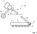
- FIG. 7 A further embodiment of the arrangement 20 is shown in Figure 7 .
- This embodiment does not form part of the claimed invention.
- the IR light 13 is sent from the light source 18 to the top face 4 of the semiconductor device 2 and into the semiconductor device 2 under an angle ⁇ .
- the IR-light 13 propagates through the semiconductor device 2 and is focused on one of the side faces 3 1 , 3 2 , 3 3 and 3 4 of the semiconductor device 2, respectively.
- the interior cracks or defects 9 block the IR-light 13 and change the normally diffuse illumination from one of the rough side faces 3 1 , 3 2 , 3 3 and 3 4 (see Fig. 5 ).
- a diffuse IR-light 33 shining out the semiconductor device 2 has a reduced response to external contamination of semiconductor device 2 and hence increases the signal to noise ratio for the real defects 9.
- FIG 8 shows a schematic representation of a further embodiment of an arrangement 20 of the present invention.
- the camera 6 has a line sensor 36 and the lens 7 images a line 35 of one of the side face 3 1 , 3 2 , 3 3 or 3 4 on the line sensor 36.
- the camera 6 is configured as a line scan camera.
- the camera 6 is moved along a scan direction 37.
- the movement can be achieved by a relative motion between the respective side face 3 1 , 3 2 , 3 3 or 3 4 of the semiconductor device 2 and the camera 6 along the scan direction 37, which is perpendicular to the line 35 to be imaged on the line sensor 36.
- the relative motion between the respective side face 3 1 , 3 2 , 3 3 or 3 4 of the semiconductor device 2 and the camera 6 should not be regarded as a limitation of the invention. It is clear that also only the camera or only the semiconductor device can be moved.
- the semiconductor device 2 is positioned on a X, Y, Theta-stage (not shown here).
- the X, Y, Theta-stage is moved such that images of all four side faces 3 1 , 3 2 , 3 3 or 3 4 are created with the line sensor 36 of the camera 6.
- the semiconductor device 2 is composed of a bulk semiconductor layer 40 (BSL), which is optional, silicon substrate 41, a dielectric layer 42 and a metal layer 43.
- BSL bulk semiconductor layer 40
- With the line scan camera setup high resolution images are possible which would be impossible with an area scan camera.
- external IR-light 13 is shining from the light source 18 through the semiconductor device 2 (die).
- the IR-light 13 comes from one side face 3 1 , 3 2 , 3 3 or 3 4 of the semiconductor device 2 and is captured at the opposite side face 3 1 , 3 2 , 3 3 or 3 4 of the semiconductor device 2 by the line scan camera 6.
- a high resolution image is created from each side face 3 1 , 3 2 , 3 3 or 3 4 of the semiconductor device 2.
- a wavelength range is used for which the semiconductor device 2 is transparent. For a typical semiconductor device 2 (or die) this will be IR light 13.
- Figure 9 is a schematic representation of an arrangement 20 for carrying out edge inspection of a semiconductor device 2 with IR illumination in side view and a scanning motion of the semiconductor device 2.
- the camera 6 has as well a line sensor 36 and the lens 7 images a line 35 of the top face 4 close to one of the side faces 3 1 , 3 2 , 3 3 or 3 4 on the line sensor 36.
- a beam splitter 27 directs the IR-light 13 from the light source 18 onto the top face 4 of the semiconductor device 2.
- Coaxial returning IR light 34 from the top face 4 of the semiconductor device 2 is captured by the line sensor 36 of the camera 6.
- the movement of the semiconductor device 2 along the scan direction 37 is perpendicular to the line 35 which is imaged on the line sensor 36 of the camera 6.
- the movement of the semiconductor device 2 enables the creation of a top view of an edge portion 30 of the top face 4 of the semiconductor device 2 at one of the side faces 3 1 , 3 2 , 3 3 or 3 4 .
- the edge portion 30 of the top face 4 is adjacent to the fourth side face 3 4 of the semiconductor device 2.
- the embodiment shown in Figure 10 shows an arrangement 20 for carrying out side view and top view inspection of the semiconductor device 2, simultaneously.
- a special optical setup 25 is provided which allows a simultaneous view on the top face 4 and one of the side faces 3 1 , 3 2 , 3 3 or 3 4 of the semiconductor device 2.
- This optical setup 25 also allows for illumination of the top face 4 (coaxial illumination) and for illumination of one of the side faces 3 1 , 3 2 , 3 3 or 3 4 (external illumination) of the semiconductor device 2.
- the two illumination modes can have the same light source or individual light sources.
- the images of the top face 4 and the side faces 3 1 , 3 2 , 3 3 or 3 4 contain much more information in order to extract the exact location and origin of the defects.
- high speed inspection can still be obtained although with two high resolution views.
- light guides 50 are used for transporting the IR-light 13.
- the light guides 50 are positioned as close as possible to the semiconductor device 2 in order to illuminate the edge portion 30 of the top face 4 and one of neighboring the side faces 3 1 , 3 2 , 3 3 or 3 4 with the IR-light 13.
- Figure 11 shows a perspective view of the apparatus for carrying out a side view of at least one of the side faces 3 1 , 3 2 , 3 3 or 3 4 of the semiconductor device 2.
- the semiconductor device 2 (not shown here) is placed on a hold with a chuck 45.
- the chuck 45 is mounted on a theta stage 38, which can be moved linearly at least in the X-coordinate direction X and the Y-coordinate direction Y. In addition a tilt is possible as well.
- a linear movement in the Z-coordinate direction Z can be integrated as well.
- a light source 18 directs the illumination light 13 to the semiconductor device 2 on the chuck 45.
- the light source 18 is arranged such that one side face 3 1 , 3 2 , 3 3 or 3 4 of the semiconductor device 2 is illuminated.
- the arrangement of the light source 18 is called backlight arrangement.
- the arrangement 20 with the optical setup 25 is arranged in order to receive the light exiting one side face 3 1 , 3 2 , 3 3 or 3 4 of the semiconductor device 2 which is opposite the illuminated side face 3 1 , 3 2 , 3 3 or 3 4 of the semiconductor device 2.
- the optical setup 25 is positioned at the front end 39 of the arrangement 20.
- the arrangement 20 is connected to a computer 32 which receives the image data from the arrangement 20. Additionally, the computer 32 is connected to a control 31 for moving the stage 38, so that the respective side face 3 1 , 3 2 , 3 3 or 3 4 is scanned by the arrangement 20.
- FIG. 12 A detailed view of the optical setup 25 of the arrangement 20 is shown in Figure 12 .
- the optical setup 25 allows a simultaneous side view and top view inspection of the semiconductor device 2.
- the optical setup 25 generates simultaneously an image of a line of light exiting a side face 3 1 , 3 2 , 3 3 or 3 4 of the semiconductor device 2 and an image of a line of light from at least a portion of a top face 4 of the semiconductor device 2.
- the line of light from a top face 4 is positioned adjacent to the line of light of the respective side face 3 1 , 3 2 , 3 3 or 3 4 of the semiconductor device 2.
- a front end 39 of the optical setup 25 carries a top mirror 51, a first bottom mirror 52, and a second bottom mirror 53.
- the top mirror 51 captures an image of the line of light from a portion of the top face 4 of the semiconductor device 2.
- the first bottom mirror 52 and the second bottom mirror 53 are arranged such at the front end 39 of the optical setup 25 that they can capture an image of a line of light exiting from a side face of the semiconductor device 2.
- the optical setup 25 is designed such that the image of a line of light, exiting from a side face 3 1 , 3 2 , 3 3 or 3 4 of the semiconductor device 2 and the image of a line of light from a top face 4 of the semiconductor device 2 are simultaneously in focus.
- the optical light coupling is in such a way that an optical path 54 via the top mirror 51 and an optical path 55 via first bottom mirror 52 and second bottom mirror 53 can be lighted separately.
- FIG. 13A to 13E The process to inspect the four side faces 3 1 , 3 2 , 3 3 and 3 4 and/or the edge portion 30 of the top face 4 is shown in Figures 13A to 13E .
- the stage 38 carries out a motion profile as described in the embodiment of Fig. 13A to 13E .
- the semiconductor device 2 is placed on the stage 38.
- the semiconductor device 2 can be held as well by a chuck (not shown here), which itself is mounted on the stage 38 (theta stage).
- the first side face 3 1 is parallel to an image plane 44 of the camera 6.
- a linear, relative movement 46 is carried out between the stage 38 with the semiconductor device 2 and the camera 6. During the movement 46 the image plane 44 of the camera 6 remains parallel to the first side face 3 1 .
- the stage 38 is rotated by 90° in the clockwise direction, so that the second side face 3 2 of the semiconductor device 2 is parallel to the image plane 44 of the camera 6 (see Fig. 13C ).
- an opposite, linear, relative movement 46 is carried out between the stage 38 with the semiconductor device 2 and the camera 6. During the movement 46 the image plane 44 of the camera 6 is parallel to the second side face 3 2 .
- the stage 38 is rotated by 90° so that the third side face 3 3 of the semiconductor device 2 is parallel to the image plane 44 of the camera 6 (see Fig. 13D ).
- a linear, relative movement 46 is carried out between the stage 38 with the semiconductor device 2 and the camera 6. During the movement 46 the image plane 44 of the camera 6 is parallel to the third side face 3 3 .
- the stage 38 is rotated by 90° so that the fourth side face 3 4 of the semiconductor device 2 is parallel to the image plane 44 of the camera 6 (see Fig. 13E ).
- an opposite, linear, relative movement 46 is carried out between the stage 38 with the semiconductor device 2 and the camera 6. During the movement 46 the image plane 44 of the camera 6 is parallel to the fourth side face 3 4 .
- the arrangement 20 and special optical setup 25(?) enable as well image capture of an edge portion 30 of the top face 4 of the semiconductor device 2, wherein the edge portion 30 (see Fig. 9 ) of the top face 4 is adjacent the respective side face 3 1 , 3 2 , 3 3 or 3 4 of the semiconductor device 2.
- FIG. 14A to 14F An additional embodiment of the process for scanning at least the four side faces 3 1 , 3 2 , 3 3 and 3 4 of the semiconductor device 2 is shown in Figures 14A to 14F .
- the movement of the stage (not shown here) and the semiconductor device 2, respectively, is composed of a rotational movement 56 around the center 58 of the semiconductor device 2 and a linear movement 57 of the semiconductor device 2 in the X/Y -plane, defined by the X-coordinate direction X and the Y-coordinate direction Y.
- Figure 14A shows the starting point of the process to scan the four side faces 3 1 , 3 2 , 3 3 and 3 4 of the semiconductor device 2.
- a focus point 59 of the camera (not shown here) is on the first side face 3 1 .
- Figure 14B shows the beginning of the rotational movement 56.
- the center 58 of the semiconductor device 2 is subjected to the movement 57 in the X/Y -plane simultaneously, so that the focus point 59 remains on the first side face 3 1 during the rotational movement 56.
- Figures 14C to 14E show various stages of the rotational movement 56 of the semiconductor device 2, wherein the focus point 59 remains on the second side face 3 2 during the rotational movement 56.
- Figure 14F shows the situation that the focus point 59 has reached the third side face 3 3 and is kept on the third side face 3 3 during the rotational movement 56 of the semiconductor device 2.
- the computer 32 coordinates the rotational movement 56 and the simultaneous movement 57 in the X/Y -plane, so that after a rotation of 360° of the semiconductor device 2 all four side faces 3 1 , 3 2 , 3 3 , and 3 4 have been imaged by the arrangement 20. Furthermore, the computer 32 makes sure that the focus point 59 is maintained on all four side faces 3 1 , 3 2 , 3 3 , and 3 4 during the full 360° rotation, so that a high quality image of all four side faces 3 1 , 3 2 , 3 3 , and 3 4 is obtained.
Claims (10)
- Verfahren für Fehlererkennung in einer vereinzelten Halbleitervorrichtung (2), wobei das Verfahren Folgendes umfasst:Beleuchten einer ersten Seitenfläche (32) der vereinzelten Halbleitervorrichtung (2) mit einem Beleuchtungslicht (13) unter Verwendung mindestens einer Lichtquelle (18), wobei das Beleuchtungslicht (13) derart auf die erste Seitenfläche (32) der vereinzelten Halbleitervorrichtung (2) gerichtet ist, dass das Beleuchtungslicht (13) durch die vereinzelte Halbleitervorrichtung (2) hindurchtritt und an einer zweiten Seitenfläche (34) der vereinzelten Halbleitervorrichtung, die der ersten Seitenfläche (32) gegenüberliegt, aus der vereinzelten Halbleitervorrichtung austritt, wobei das Licht als diffuser Lichtstrahl aus der zweiten Seitenfläche (34) der vereinzelten Halbleitervorrichtung (2) austritt, wobei das Beleuchtungslicht (13) entlang einer senkrecht zu der ersten Seitenfläche (32) stehenden Achse auf die erste Seitenfläche (32) der Halbleitervorrichtung (2) gerichtet ist;Abbilden des Lichts, das aus der zweiten Seitenfläche (34) der vereinzelten Halbleitervorrichtung (2) austritt, auf einen Detektor (26) einer Kamera (6) mit einem Objektiv (7), wobei die Kamera (6) mit ihrem Objektiv (7) direkt auf die zweite Seitenfläche (34) der vereinzelten Halbleitervorrichtung (2) blickt;wobei jede der Seitenflächen (31, 32, 33, 34) der vereinzelten Halbleitervorrichtung vereinzelte Kanten sind; und wobei bei Erreichen eines Innendefekts oder eines Seitenrisses der vereinzelten Halbleitervorrichtung (2) ein Teil des diffusen Strahls durch den Innendefekt (9) oder den Seitenriss, die zu einem fehlerhaften Teil im Kamerabild führen, blockiert ist;Ausführen einer Relativbewegung eines Objekttisches (38), der die vereinzelte Halbleitervorrichtung (2) und die Kamera (6) hält, sodass die zweite Seitenfläche (32) der vereinzelten Halbleitervorrichtung (2) vollständig durch die Kamera (6) abgebildet wird; undwobei der Schritt des Ausführens einer Relativbewegung des Objekttisches (38) ferner Folgendes umfasst: Drehen des Objekttisches (38) und paralleles Ausführen einer Bewegung des Objekttisches (38) in der X/Y-Ebene, sodass ein Fokuspunkt (59) der Kamera (6) während der Drehbewegung des Objekttisches (38) auf einer jeweiligen Seitenfläche (3) bleibt.
- Verfahren nach Anspruch 1, ferner umfassend:Richten des Beleuchtungslichts (13) der mindestens einen Lichtquelle (18) auf die erste Seitenfläche (32) der vereinzelten Halbleitervorrichtung (2); undAbbilden von aus der zweiten Seitenfläche (34) der vereinzelten Halbleitervorrichtung (2) austretenden Lichts mit der Kamera (6), und wobei die Kamera (6) das aus der zweiten Seitenfläche (34) der vereinzelten Halbleitervorrichtung (2) austretende Licht mittels eines Objektivs (7) auf einen Liniensensor (36) abbildet.
- Verfahren nach Anspruch 1, ferner umfassend:Ausstatten der Kamera (6) mit einem Liniensensor (36); undgleichzeitiges Generieren eines Linienbildes von Licht, das aus einer Seitenfläche (32) der vereinzelten Halbleitervorrichtung (2) austritt, und eines Linienbildes von Licht von einem Abschnitt einer Oberseite (4) der vereinzelten Halbleitervorrichtung (2) mit einer optischen Einrichtung, wobei der Abschnitt der Oberseite (4) benachbart zu der jeweiligen Seitenfläche (32) der vereinzelten Halbleitervorrichtung (2) positioniert ist.
- Verfahren nach Anspruch 1, ferner umfassend:Ausstatten der Kamera (6) mit einem Liniensensor (36); undgleichzeitiges Generieren eines Linienbildes von Licht, das aus einer Seitenfläche (3) der vereinzelten Halbleitervorrichtung (2) austritt, und eines Linienbildes von Licht von einem Abschnitt einer Oberseite (4) der vereinzelten Halbleitervorrichtung (2) mit einer optischen Einrichtung, wobei der Abschnitt der Oberseite (4) benachbart zu der jeweiligen Seitenfläche (3) der vereinzelten Halbleitervorrichtung (2) positioniert ist, undwobei ein vorderes Ende der optischen Einrichtung einen oberen Spiegel (51) und zwei untere Spiegel (52, 53) trägt und der obere Spiegel (51) ein Linienbild von Licht von einem Abschnitt der Oberseite (4) der vereinzelten Halbleitervorrichtung (2) erfasst und die zwei unteren Spiegel (52, 53) ein Linienbild von Licht, das aus einer Seitenfläche (3) der vereinzelten Halbleitervorrichtung (2) austritt, erfassen.
- Verfahren nach Anspruch 1, ferner umfassend:Ausstatten der Kamera (6) mit einem Liniensensor (36); undgleichzeitiges Generieren eines Linienbildes von Licht, das aus einer Seitenfläche der vereinzelten Halbleitervorrichtung (2) austritt, und eines Linienbildes von Licht von einem Abschnitt einer Oberseite (4) der vereinzelten Halbleitervorrichtung (2) mit einer optischen Einrichtung, wobei der Abschnitt der Oberseite (4) benachbart zu der jeweiligen Seitenfläche (3) der vereinzelten Halbleitervorrichtung (2) positioniert ist, undwobei die optische Einrichtung derart ausgestaltet ist, dass das von der Seitenfläche (3) der vereinzelten Halbleitervorrichtung (2) erfasste Linienbild und das Linienbild des Abschnitts der Oberseite (4) der vereinzelten Halbleitervorrichtung (2) gleichzeitig im Fokus sind.
- Verfahren nach Anspruch 1, ferner umfassend:
Einkoppeln von Licht von mindestens einer Lichtquelle (18) getrennt in eine Seitenfläche (3) der vereinzelten Halbleitervorrichtung (2) und die Oberseite (4) der vereinzelten Halbleitervorrichtung (2). - Verfahren nach Anspruch 1, wobei ein Lichtleiter (50) zwischen mindestens einer Lichtquelle (18) und mindestens einer von der Oberseite (4) und einer jeweiligen Seitenfläche (3) der vereinzelten Halbleitervorrichtung (2) positioniert ist.
- Verfahren nach Anspruch 1, wobei das Bewegen eines Objekttisches (38) zum Abbilden von mindestens zwei Seitenflächen (3) und des Abschnitts der jeweiligen Oberseite (4) ferner Folgendes umfasst:a) Ausführen einer linearen Relativbewegung zwischen dem Objekttisch (38) mit der vereinzelten Halbleitervorrichtung (2) und der Kamera (6), sodass eine Bildebene der Kamera (6) parallel zu einer der Seitenflächen (3) ist;b) Drehen des Objekttisches (38) mit der vereinzelten Halbleitervorrichtung (2); undc) Wiederholen der Schritte a) und b), bis alle Seitenflächen (3) der vereinzelten Halbleitervorrichtung (2) durch die Kamera (6) abgebildet sind.
- Verfahren nach Anspruch 1, wobei der Schritt des Ausführens einer Relativbewegung des Objekttisches (36) zum Abbilden von mindestens zwei Seitenflächen (3) und des Abschnitts der jeweiligen Oberseite (4) ferner Folgendes umfasst:a) Ausführen einer linearen Relativbewegung zwischen dem Objekttisch (38) mit der vereinzelten Halbleitervorrichtung (2) und der Kamera (6), sodass eine Bildebene der Kamera (6) parallel zu einer der Seitenflächen (3) ist;b) Drehen des Objekttisches (38) mit der vereinzelten Halbleitervorrichtung (2); undc) Wiederholen der vorstehenden Schritte, bis alle Seitenflächen (3) der vereinzelten Halbleitervorrichtung (2) durch die Kamera (6) abgebildet sind, undwobei die lineare Relativbewegung zwischen dem Objekttisch (36) und der Kamera (6) nur durch eine lineare Bewegung der Kamera (6) realisiert wird und die lineare Bewegung der Kamera (6) zwischen nachfolgenden Vorgängen des Schritts des Drehens des Objekttisches (36) in entgegengesetzte Richtungen orientiert ist.
- Verfahren nach Anspruch 1, wobei der Wellenlängenbereich des Beleuchtungslichts (13) ein Wellenlängenbereich von IR-Licht ist.
Priority Applications (2)
| Application Number | Priority Date | Filing Date | Title |
|---|---|---|---|
| EP21190120.2A EP3926330A1 (de) | 2014-12-05 | 2015-12-04 | Gerät und verfahren zur defekterkennung in werkstücken |
| EP24160048.5A EP4354162A2 (de) | 2014-12-05 | 2015-12-04 | Vorrichtung, verfahren und computerprogrammprodukt für fehlerbehebung erkennung in werkstücken |
Applications Claiming Priority (3)
| Application Number | Priority Date | Filing Date | Title |
|---|---|---|---|
| US201462088284P | 2014-12-05 | 2014-12-05 | |
| US201562154109P | 2015-04-28 | 2015-04-28 | |
| PCT/US2015/064100 WO2016090311A1 (en) | 2014-12-05 | 2015-12-04 | Apparatus, method and computer program product for defect detection in work pieces |
Related Child Applications (3)
| Application Number | Title | Priority Date | Filing Date |
|---|---|---|---|
| EP21190120.2A Division EP3926330A1 (de) | 2014-12-05 | 2015-12-04 | Gerät und verfahren zur defekterkennung in werkstücken |
| EP21190120.2A Division-Into EP3926330A1 (de) | 2014-12-05 | 2015-12-04 | Gerät und verfahren zur defekterkennung in werkstücken |
| EP24160048.5A Division EP4354162A2 (de) | 2014-12-05 | 2015-12-04 | Vorrichtung, verfahren und computerprogrammprodukt für fehlerbehebung erkennung in werkstücken |
Publications (3)
| Publication Number | Publication Date |
|---|---|
| EP3164723A1 EP3164723A1 (de) | 2017-05-10 |
| EP3164723A4 EP3164723A4 (de) | 2018-07-25 |
| EP3164723B1 true EP3164723B1 (de) | 2024-02-28 |
Family
ID=56092564
Family Applications (3)
| Application Number | Title | Priority Date | Filing Date |
|---|---|---|---|
| EP15865251.1A Active EP3164723B1 (de) | 2014-12-05 | 2015-12-04 | Verfahren für fehlererkennung in werkstücken |
| EP21190120.2A Pending EP3926330A1 (de) | 2014-12-05 | 2015-12-04 | Gerät und verfahren zur defekterkennung in werkstücken |
| EP24160048.5A Pending EP4354162A2 (de) | 2014-12-05 | 2015-12-04 | Vorrichtung, verfahren und computerprogrammprodukt für fehlerbehebung erkennung in werkstücken |
Family Applications After (2)
| Application Number | Title | Priority Date | Filing Date |
|---|---|---|---|
| EP21190120.2A Pending EP3926330A1 (de) | 2014-12-05 | 2015-12-04 | Gerät und verfahren zur defekterkennung in werkstücken |
| EP24160048.5A Pending EP4354162A2 (de) | 2014-12-05 | 2015-12-04 | Vorrichtung, verfahren und computerprogrammprodukt für fehlerbehebung erkennung in werkstücken |
Country Status (10)
| Country | Link |
|---|---|
| US (6) | US10324044B2 (de) |
| EP (3) | EP3164723B1 (de) |
| JP (5) | JP6929772B2 (de) |
| KR (8) | KR20230105688A (de) |
| CN (3) | CN113702389A (de) |
| MY (3) | MY188685A (de) |
| PH (2) | PH12017501024A1 (de) |
| SG (3) | SG10202110739PA (de) |
| TW (2) | TWI663394B (de) |
| WO (1) | WO2016090311A1 (de) |
Families Citing this family (19)
| Publication number | Priority date | Publication date | Assignee | Title |
|---|---|---|---|---|
| SG10202110739PA (en) | 2014-12-05 | 2021-11-29 | Kla Tencor Corp | Apparatus, method and computer program product for defect detection in work pieces |
| US10670531B2 (en) * | 2016-01-04 | 2020-06-02 | Laser & Plasma Technologies, LLC | Infrared detection camera |
| CN107843991A (zh) * | 2017-09-05 | 2018-03-27 | 努比亚技术有限公司 | 屏幕漏光的检测方法、系统、终端及计算机可读存储介质 |
| WO2019157271A2 (en) * | 2018-02-09 | 2019-08-15 | Massachusetts Institute Of Technology | Systems and methods for crack detection |
| US20190257876A1 (en) * | 2018-02-21 | 2019-08-22 | Asm Technology Singapore Pte Ltd | System and method for detecting defects in an electronic device |
| CN108872246A (zh) * | 2018-05-29 | 2018-11-23 | 湖南科创信息技术股份有限公司 | 板面材料全视面缺陷检测系统 |
| CN109100366A (zh) * | 2018-08-10 | 2018-12-28 | 武汉盛为芯科技有限公司 | 半导体激光器芯片端面外观的检测系统及方法 |
| US10481097B1 (en) * | 2018-10-01 | 2019-11-19 | Guardian Glass, LLC | Method and system for detecting inclusions in float glass based on spectral reflectance analysis |
| US10746667B2 (en) * | 2018-11-27 | 2020-08-18 | General Electric Company | Fluorescent penetrant inspection system and method |
| US11609187B2 (en) * | 2019-05-15 | 2023-03-21 | Getac Technology Corporation | Artificial neural network-based method for selecting surface type of object |
| US11543363B2 (en) | 2019-05-24 | 2023-01-03 | Taiwan Semiconductor Manufacturing Co., Ltd. | Systems and methods for wafer bond monitoring |
| US11340284B2 (en) * | 2019-07-23 | 2022-05-24 | Kla Corporation | Combined transmitted and reflected light imaging of internal cracks in semiconductor devices |
| JP6755603B1 (ja) | 2019-12-25 | 2020-09-16 | 上野精機株式会社 | 電子部品の処理装置 |
| JP7437987B2 (ja) * | 2020-03-23 | 2024-02-26 | ファスフォードテクノロジ株式会社 | ダイボンディング装置および半導体装置の製造方法 |
| KR102255421B1 (ko) * | 2020-08-11 | 2021-05-24 | 충남대학교산학협력단 | 단결정 산화갈륨의 결함 평가방법 |
| JP2022137904A (ja) * | 2021-03-09 | 2022-09-22 | 本田技研工業株式会社 | 表面検査方法及び表面検査装置 |
| JP6906779B1 (ja) * | 2021-03-11 | 2021-07-21 | ヴィスコ・テクノロジーズ株式会社 | 半導体チップの検査方法及び装置 |
| TWI797689B (zh) * | 2021-05-24 | 2023-04-01 | 馬來西亞商正齊科技有限公司 | 檢查電子元件內部缺陷的裝置及方法 |
| CN116757973B (zh) * | 2023-08-23 | 2023-12-01 | 成都数之联科技股份有限公司 | 一种面板产品自动修补方法、系统、设备及存储介质 |
Citations (2)
| Publication number | Priority date | Publication date | Assignee | Title |
|---|---|---|---|---|
| US20070257192A1 (en) * | 2006-05-08 | 2007-11-08 | Mitsubishi Electric Corporation | Image inspection device and image inspection method using the image inspection device |
| DE102009017786B3 (de) * | 2009-04-20 | 2010-10-14 | Intego Gmbh | Verfahren zur Detektion von Fehlstellen in einer dünnen Waferscheibe für ein Solarelement sowie Vorrichtung zur Durchführung des Verfahrens |
Family Cites Families (71)
| Publication number | Priority date | Publication date | Assignee | Title |
|---|---|---|---|---|
| DE1623425C2 (de) | 1967-10-26 | 1972-06-08 | Eltro Gmbh | Optoelektronisches Verfahren und System zur Durchfuehrung dieses Verfahrens |
| US4689491A (en) * | 1985-04-19 | 1987-08-25 | Datasonics Corp. | Semiconductor wafer scanning system |
| US4891530A (en) | 1986-02-22 | 1990-01-02 | Helmut K. Pinsch Gmbh & Co. | Testing or inspecting apparatus and method for detecting differently shaped surfaces of objects |
| JP2591751B2 (ja) | 1987-06-29 | 1997-03-19 | 日本電気株式会社 | オブジェクト間の類似度判定方式 |
| JPH02281132A (ja) * | 1989-04-21 | 1990-11-16 | Matsushita Electric Ind Co Ltd | 汚れ検出器 |
| JP2975476B2 (ja) * | 1992-03-30 | 1999-11-10 | 三井金属鉱業株式会社 | 結晶内のフォトルミネッセンス計測方法及び装置 |
| JP2847458B2 (ja) * | 1993-03-26 | 1999-01-20 | 三井金属鉱業株式会社 | 欠陥評価装置 |
| JP3366067B2 (ja) * | 1993-09-03 | 2003-01-14 | ラトックシステムエンジニアリング株式会社 | 結晶欠陥検出方法 |
| JP3348168B2 (ja) * | 1993-09-03 | 2002-11-20 | ラトックシステムエンジニアリング株式会社 | 結晶欠陥検出方法およびその装置 |
| US5790247A (en) * | 1995-10-06 | 1998-08-04 | Photon Dynamics, Inc. | Technique for determining defect positions in three dimensions in a transparent structure |
| WO1998037404A1 (en) * | 1997-02-21 | 1998-08-27 | Sidney Braginsky | Method of scanning semiconductor wafers to inspect for defects |
| JP2897754B2 (ja) | 1997-03-27 | 1999-05-31 | 日本電気株式会社 | 半導体装置の検査方法 |
| JPH11352072A (ja) * | 1998-06-04 | 1999-12-24 | Advantest Corp | 表面検査装置および方法 |
| US6529018B1 (en) | 1998-08-28 | 2003-03-04 | International Business Machines Corporation | Method for monitoring defects in polysilicon gates in semiconductor devices responsive to illumination by incident light |
| DE69800756T2 (de) | 1998-10-15 | 2001-08-09 | Wacker Siltronic Halbleitermat | Verfahren und Vorrichtung zum Detektieren, Überwachung und Charakterisierung von Kantendefekten in Halbleiterscheiben |
| US6384415B1 (en) | 2000-06-20 | 2002-05-07 | Kabushiki Kaisha Kobe Seiko Sho (Kobe Steel, Ltd.) | Method of evaluating quality of silicon wafer and method of reclaiming the water |
| US6512239B1 (en) * | 2000-06-27 | 2003-01-28 | Photon Dynamics Canada Inc. | Stereo vision inspection system for transparent media |
| JP2002310929A (ja) * | 2001-04-13 | 2002-10-23 | Mitsubishi Electric Corp | 欠陥検査装置 |
| JP3709426B2 (ja) | 2001-11-02 | 2005-10-26 | 日本エレクトロセンサリデバイス株式会社 | 表面欠陥検出方法および表面欠陥検出装置 |
| JP3762952B2 (ja) * | 2002-09-04 | 2006-04-05 | レーザーテック株式会社 | 光学装置並びにそれを用いた画像測定装置及び検査装置 |
| US20040207836A1 (en) * | 2002-09-27 | 2004-10-21 | Rajeshwar Chhibber | High dynamic range optical inspection system and method |
| US7339661B2 (en) * | 2002-09-30 | 2008-03-04 | Doron Korngut | Dark field inspection system |
| WO2004072629A1 (en) | 2003-02-17 | 2004-08-26 | Nanyang Technological University | System and method for inspection of silicon wafers |
| JP2005257671A (ja) | 2004-02-10 | 2005-09-22 | Sharp Corp | 光学部品の欠陥検出方法および欠陥検出装置 |
| DE102004029212B4 (de) | 2004-06-16 | 2006-07-13 | Leica Microsystems Semiconductor Gmbh | Vorrichtung und Verfahren zur optischen Auf- und/oder Durchlichtinspektion von Mikrostrukturen im IR |
| JP4626982B2 (ja) | 2005-02-10 | 2011-02-09 | セントラル硝子株式会社 | ガラス板の端面の欠陥検出装置および検出方法 |
| US7898650B2 (en) * | 2005-02-18 | 2011-03-01 | Hoya Corporation | Inspection method for transparent article |
| JP2007086050A (ja) * | 2005-02-18 | 2007-04-05 | Hoya Corp | 透光性材料からなる透光性物品の検査方法、ガラス基板の欠陥検査方法及び装置、マスクブランク用ガラス基板の製造方法、マスクブランクの製造方法、及び露光用マスクの製造方法、並びに、マスクブランク用ガラス基板、マスクブランク、露光用マスク、及び半導体装置の製造方法 |
| CN2791639Y (zh) | 2005-03-02 | 2006-06-28 | 昆明物理研究所 | 检测半导体材料内部缺陷的红外装置 |
| JP2006351669A (ja) * | 2005-06-14 | 2006-12-28 | Mitsubishi Electric Corp | 赤外検査装置および赤外検査方法ならびに半導体ウェハの製造方法 |
| JP4847128B2 (ja) | 2005-12-21 | 2011-12-28 | 日本エレクトロセンサリデバイス株式会社 | 表面欠陥検査装置 |
| JP4973062B2 (ja) | 2006-08-14 | 2012-07-11 | ヤマハ株式会社 | 半導体チップの検査方法及びウェハのクラック検査装置 |
| KR20080015363A (ko) | 2006-08-14 | 2008-02-19 | 야마하 가부시키가이샤 | 웨이퍼 및 반도체 소자의 검사 방법 및 장치 |
| KR100768038B1 (ko) * | 2006-10-24 | 2007-10-17 | 한국전기연구원 | 균일한 내부 전반사 조명에 의한 바이오칩 측정 장치 및방법 |
| US8274727B1 (en) | 2006-11-13 | 2012-09-25 | Hrl Laboratories, Llc | Programmable optical label |
| CN101021490B (zh) * | 2007-03-12 | 2012-11-14 | 3i系统公司 | 平面基板自动检测系统及方法 |
| US8023111B2 (en) * | 2007-04-27 | 2011-09-20 | Shibaura Mechatronics Corporation | Surface inspection apparatus |
| TW200907335A (en) | 2007-05-21 | 2009-02-16 | Nikon Corp | Wafer end surface inspecting apparatus |
| WO2009021207A2 (en) | 2007-08-09 | 2009-02-12 | Accretech Usa, Inc. | Apparatus and method for wafer edge exclusion measurement |
| JP4600476B2 (ja) * | 2007-12-28 | 2010-12-15 | 日本電気株式会社 | 微細構造物の欠陥検査方法及び欠陥検査装置 |
| JP2009192358A (ja) * | 2008-02-14 | 2009-08-27 | Fuji Electric Systems Co Ltd | 欠陥検査装置 |
| JP2009236493A (ja) * | 2008-03-25 | 2009-10-15 | Mitsubishi Rayon Co Ltd | 透明板の欠陥検査方法および装置 |
| JP5240771B2 (ja) * | 2008-04-14 | 2013-07-17 | 上野精機株式会社 | 外観検査装置 |
| JP2010025713A (ja) * | 2008-07-18 | 2010-02-04 | Hitachi High-Technologies Corp | 欠陥検査方法及び欠陥検査装置 |
| TWI512865B (zh) | 2008-09-08 | 2015-12-11 | Rudolph Technologies Inc | 晶圓邊緣檢查技術 |
| US8532364B2 (en) | 2009-02-18 | 2013-09-10 | Texas Instruments Deutschland Gmbh | Apparatus and method for detecting defects in wafer manufacturing |
| CN101819165B (zh) * | 2009-02-27 | 2013-08-07 | 圣戈本玻璃法国公司 | 用于检测图案化基板的缺陷的方法及系统 |
| KR101114362B1 (ko) * | 2009-03-09 | 2012-02-14 | 주식회사 쓰리비 시스템 | 결점검사를 위한 검사장치 |
| KR101323035B1 (ko) * | 2009-05-29 | 2013-10-29 | 로세브 테크놀로지 코포레이션 | 다결정 웨이퍼의 검사 방법 |
| JP2011033449A (ja) | 2009-07-31 | 2011-02-17 | Sumco Corp | ウェーハの欠陥検査方法及び欠陥検査装置 |
| DE102009050711A1 (de) * | 2009-10-26 | 2011-05-05 | Schott Ag | Verfahren und Vorrichtung zur Detektion von Rissen in Halbleitersubstraten |
| KR20110055788A (ko) * | 2009-11-20 | 2011-05-26 | 재단법인 서울테크노파크 | 레이저를 이용한 접합웨이퍼 검사방법 |
| KR101519476B1 (ko) | 2010-02-17 | 2015-05-14 | 한미반도체 주식회사 | 잉곳 검사 장치 및 방법 |
| KR101214806B1 (ko) * | 2010-05-11 | 2012-12-24 | 가부시키가이샤 사무코 | 웨이퍼 결함 검사 장치 및 웨이퍼 결함 검사 방법 |
| TWI422814B (zh) * | 2010-08-23 | 2014-01-11 | Delta Electronics Inc | 基板內部缺陷檢查裝置及方法 |
| JP2012083125A (ja) | 2010-10-07 | 2012-04-26 | Nikon Corp | 端面検査装置 |
| US9001029B2 (en) | 2011-02-15 | 2015-04-07 | Basf Se | Detector for optically detecting at least one object |
| JPWO2012153718A1 (ja) | 2011-05-12 | 2014-07-31 | コニカミノルタ株式会社 | ガラスシートの端面検査方法、及びガラスシートの端面検査装置 |
| WO2012176106A2 (en) * | 2011-06-24 | 2012-12-27 | Kla-Tencor Corporation | Method and apparatus for inspection of light emitting semiconductor devices using photoluminescence imaging |
| JP2013015428A (ja) | 2011-07-05 | 2013-01-24 | Lasertec Corp | 検査装置、検査方法及び半導体装置の製造方法 |
| JP5594254B2 (ja) | 2011-08-09 | 2014-09-24 | 三菱電機株式会社 | シリコン基板の検査装置、および検査方法 |
| CN103376259A (zh) | 2012-04-11 | 2013-10-30 | 百励科技股份有限公司 | 元件内部缺陷的检测装置及方法 |
| PL222470B1 (pl) | 2012-08-14 | 2016-07-29 | Włodarczyk Władysław Igloo | Moduł głowicy do pobierania oraz umieszczania komponentów dedykowanych w technologii SMT |
| WO2014052811A1 (en) | 2012-09-28 | 2014-04-03 | Rudolph Technologies, Inc. | Inspection of substrates using calibration and imaging |
| CN203011849U (zh) | 2012-11-13 | 2013-06-19 | 上海太阳能工程技术研究中心有限公司 | 硅片缺陷检测装置 |
| KR20140060946A (ko) * | 2012-11-13 | 2014-05-21 | 에이티아이 주식회사 | 전자재료 가공부위 측정용 조명장치 및 이를 적용한 검사 장치 |
| KR101385219B1 (ko) | 2012-12-27 | 2014-04-16 | 한국생산기술연구원 | 반도체 패키지의 결함 검출 시스템 및 결함 검출 방법 |
| US9041919B2 (en) | 2013-02-18 | 2015-05-26 | Globalfoundries Inc. | Infrared-based metrology for detection of stress and defects around through silicon vias |
| DE102013108308A1 (de) * | 2013-08-01 | 2015-02-19 | Schott Ag | Verfahren und Vorrichtung zur Detektion in Bandrollen aus sprödhartem oder sprödbrechendem, zumindest teiltransparentem Material, sowie deren Verwendung |
| SG10202110739PA (en) | 2014-12-05 | 2021-11-29 | Kla Tencor Corp | Apparatus, method and computer program product for defect detection in work pieces |
| KR102093450B1 (ko) | 2018-12-31 | 2020-03-25 | 주식회사 디쓰리디 | 원단의 물성 측정 시스템 및 방법 |
-
2015
- 2015-12-04 SG SG10202110739PA patent/SG10202110739PA/en unknown
- 2015-12-04 KR KR1020237022390A patent/KR20230105688A/ko not_active Application Discontinuation
- 2015-12-04 MY MYPI2021001771A patent/MY188685A/en unknown
- 2015-12-04 EP EP15865251.1A patent/EP3164723B1/de active Active
- 2015-12-04 KR KR1020217042849A patent/KR20220003134A/ko not_active IP Right Cessation
- 2015-12-04 WO PCT/US2015/064100 patent/WO2016090311A1/en active Application Filing
- 2015-12-04 KR KR1020237034587A patent/KR20230146671A/ko not_active Application Discontinuation
- 2015-12-04 JP JP2017529614A patent/JP6929772B2/ja active Active
- 2015-12-04 KR KR1020227023564A patent/KR102589607B1/ko active IP Right Grant
- 2015-12-04 KR KR1020227023565A patent/KR20220103201A/ko not_active Application Discontinuation
- 2015-12-04 SG SG11201704388YA patent/SG11201704388YA/en unknown
- 2015-12-04 SG SG10201913246TA patent/SG10201913246TA/en unknown
- 2015-12-04 KR KR1020227023563A patent/KR20220103199A/ko not_active Application Discontinuation
- 2015-12-04 KR KR1020177018489A patent/KR102386192B1/ko active IP Right Grant
- 2015-12-04 MY MYPI2017000150A patent/MY181846A/en unknown
- 2015-12-04 TW TW104140838A patent/TWI663394B/zh active
- 2015-12-04 CN CN202111010485.9A patent/CN113702389A/zh active Pending
- 2015-12-04 KR KR1020227011485A patent/KR20220047684A/ko active Application Filing
- 2015-12-04 MY MYPI2020006001A patent/MY185911A/en unknown
- 2015-12-04 EP EP21190120.2A patent/EP3926330A1/de active Pending
- 2015-12-04 TW TW108116788A patent/TWI702390B/zh active
- 2015-12-04 CN CN201580065271.8A patent/CN107003254A/zh active Pending
- 2015-12-04 CN CN202110040476.8A patent/CN112858319A/zh active Pending
- 2015-12-04 EP EP24160048.5A patent/EP4354162A2/de active Pending
-
2016
- 2016-07-01 US US15/200,613 patent/US10324044B2/en active Active
-
2017
- 2017-06-02 PH PH12017501024A patent/PH12017501024A1/en unknown
-
2019
- 2019-06-17 US US16/443,616 patent/US10935503B2/en active Active
-
2020
- 2020-08-26 PH PH12020551338A patent/PH12020551338A1/en unknown
- 2020-10-07 US US17/065,466 patent/US11892493B2/en active Active
- 2020-11-02 US US17/087,421 patent/US11105839B2/en active Active
-
2021
- 2021-08-11 JP JP2021131177A patent/JP7373527B2/ja active Active
- 2021-08-11 JP JP2021131178A patent/JP2021175987A/ja active Pending
- 2021-12-10 US US17/548,255 patent/US11726126B2/en active Active
-
2023
- 2023-08-14 US US18/233,807 patent/US20230393185A1/en active Pending
- 2023-10-23 JP JP2023181884A patent/JP2023174984A/ja active Pending
-
2024
- 2024-01-16 JP JP2024004513A patent/JP2024026780A/ja active Pending
Patent Citations (2)
| Publication number | Priority date | Publication date | Assignee | Title |
|---|---|---|---|---|
| US20070257192A1 (en) * | 2006-05-08 | 2007-11-08 | Mitsubishi Electric Corporation | Image inspection device and image inspection method using the image inspection device |
| DE102009017786B3 (de) * | 2009-04-20 | 2010-10-14 | Intego Gmbh | Verfahren zur Detektion von Fehlstellen in einer dünnen Waferscheibe für ein Solarelement sowie Vorrichtung zur Durchführung des Verfahrens |
Also Published As
Similar Documents
| Publication | Publication Date | Title |
|---|---|---|
| US11892493B2 (en) | Apparatus, method and computer program product for defect detection in work pieces | |
| US7973921B2 (en) | Dynamic illumination in optical inspection systems | |
| US9140545B2 (en) | Object inspection system | |
| JP2019049520A (ja) | マルチモードシステムおよび方法 | |
| CN215525579U (zh) | 一种检测设备 | |
| CN115561255A (zh) | 检测设备及检测方法、检测系统及存储介质 | |
| KR20180136381A (ko) | 멀티 모드 시스템 및 방법 | |
| KR20230056770A (ko) | 높은 처리량 광학 계측 |
Legal Events
| Date | Code | Title | Description |
|---|---|---|---|
| STAA | Information on the status of an ep patent application or granted ep patent |
Free format text: STATUS: THE INTERNATIONAL PUBLICATION HAS BEEN MADE |
|
| PUAI | Public reference made under article 153(3) epc to a published international application that has entered the european phase |
Free format text: ORIGINAL CODE: 0009012 |
|
| STAA | Information on the status of an ep patent application or granted ep patent |
Free format text: STATUS: REQUEST FOR EXAMINATION WAS MADE |
|
| 17P | Request for examination filed |
Effective date: 20170206 |
|
| AK | Designated contracting states |
Kind code of ref document: A1 Designated state(s): AL AT BE BG CH CY CZ DE DK EE ES FI FR GB GR HR HU IE IS IT LI LT LU LV MC MK MT NL NO PL PT RO RS SE SI SK SM TR |
|
| AX | Request for extension of the european patent |
Extension state: BA ME |
|
| DAV | Request for validation of the european patent (deleted) | ||
| DAX | Request for extension of the european patent (deleted) | ||
| RIC1 | Information provided on ipc code assigned before grant |
Ipc: G01R 31/28 20060101ALI20180227BHEP Ipc: G01N 21/88 20060101AFI20180227BHEP Ipc: G01R 31/01 20060101ALI20180227BHEP Ipc: G01N 21/95 20060101ALI20180227BHEP Ipc: G01R 31/26 20140101ALI20180227BHEP |
|
| A4 | Supplementary search report drawn up and despatched |
Effective date: 20180621 |
|
| RIC1 | Information provided on ipc code assigned before grant |
Ipc: G01R 31/28 20060101ALI20180615BHEP Ipc: G01N 21/95 20060101ALI20180615BHEP Ipc: G01R 31/01 20060101ALI20180615BHEP Ipc: G01N 21/88 20060101AFI20180615BHEP Ipc: G01R 31/26 20140101ALI20180615BHEP |
|
| STAA | Information on the status of an ep patent application or granted ep patent |
Free format text: STATUS: EXAMINATION IS IN PROGRESS |
|
| 17Q | First examination report despatched |
Effective date: 20181220 |
|
| STAA | Information on the status of an ep patent application or granted ep patent |
Free format text: STATUS: EXAMINATION IS IN PROGRESS |
|
| STAA | Information on the status of an ep patent application or granted ep patent |
Free format text: STATUS: EXAMINATION IS IN PROGRESS |
|
| P01 | Opt-out of the competence of the unified patent court (upc) registered |
Effective date: 20230526 |
|
| GRAP | Despatch of communication of intention to grant a patent |
Free format text: ORIGINAL CODE: EPIDOSNIGR1 |
|
| STAA | Information on the status of an ep patent application or granted ep patent |
Free format text: STATUS: GRANT OF PATENT IS INTENDED |
|
| INTG | Intention to grant announced |
Effective date: 20230911 |
|
| GRAS | Grant fee paid |
Free format text: ORIGINAL CODE: EPIDOSNIGR3 |
|
| GRAA | (expected) grant |
Free format text: ORIGINAL CODE: 0009210 |
|
| STAA | Information on the status of an ep patent application or granted ep patent |
Free format text: STATUS: THE PATENT HAS BEEN GRANTED |
|
| AK | Designated contracting states |
Kind code of ref document: B1 Designated state(s): AL AT BE BG CH CY CZ DE DK EE ES FI FR GB GR HR HU IE IS IT LI LT LU LV MC MK MT NL NO PL PT RO RS SE SI SK SM TR |
|
| REG | Reference to a national code |
Ref country code: GB Ref legal event code: FG4D |
|
| REG | Reference to a national code |
Ref country code: CH Ref legal event code: EP |
|
| REG | Reference to a national code |
Ref country code: DE Ref legal event code: R096 Ref document number: 602015087741 Country of ref document: DE |
|
| REG | Reference to a national code |
Ref country code: IE Ref legal event code: FG4D |