EP3142124B1 - Anisotropic conductive material and an electronic device including anisotropic conductive material - Google Patents
Anisotropic conductive material and an electronic device including anisotropic conductive material Download PDFInfo
- Publication number
- EP3142124B1 EP3142124B1 EP16167463.5A EP16167463A EP3142124B1 EP 3142124 B1 EP3142124 B1 EP 3142124B1 EP 16167463 A EP16167463 A EP 16167463A EP 3142124 B1 EP3142124 B1 EP 3142124B1
- Authority
- EP
- European Patent Office
- Prior art keywords
- conductive material
- anisotropic conductive
- electrode portion
- example embodiments
- particles
- Prior art date
- Legal status (The legal status is an assumption and is not a legal conclusion. Google has not performed a legal analysis and makes no representation as to the accuracy of the status listed.)
- Active
Links
Images


Classifications
-
- H10W72/30—
-
- H—ELECTRICITY
- H01—ELECTRIC ELEMENTS
- H01B—CABLES; CONDUCTORS; INSULATORS; SELECTION OF MATERIALS FOR THEIR CONDUCTIVE, INSULATING OR DIELECTRIC PROPERTIES
- H01B5/00—Non-insulated conductors or conductive bodies characterised by their form
- H01B5/16—Non-insulated conductors or conductive bodies characterised by their form comprising conductive material in insulating or poorly conductive material, e.g. conductive rubber
-
- H—ELECTRICITY
- H01—ELECTRIC ELEMENTS
- H01B—CABLES; CONDUCTORS; INSULATORS; SELECTION OF MATERIALS FOR THEIR CONDUCTIVE, INSULATING OR DIELECTRIC PROPERTIES
- H01B1/00—Conductors or conductive bodies characterised by the conductive materials; Selection of materials as conductors
- H01B1/20—Conductive material dispersed in non-conductive organic material
- H01B1/22—Conductive material dispersed in non-conductive organic material the conductive material comprising metals or alloys
-
- H—ELECTRICITY
- H01—ELECTRIC ELEMENTS
- H01R—ELECTRICALLY-CONDUCTIVE CONNECTIONS; STRUCTURAL ASSOCIATIONS OF A PLURALITY OF MUTUALLY-INSULATED ELECTRICAL CONNECTING ELEMENTS; COUPLING DEVICES; CURRENT COLLECTORS
- H01R4/00—Electrically-conductive connections between two or more conductive members in direct contact, i.e. touching one another; Means for effecting or maintaining such contact; Electrically-conductive connections having two or more spaced connecting locations for conductors and using contact members penetrating insulation
- H01R4/04—Electrically-conductive connections between two or more conductive members in direct contact, i.e. touching one another; Means for effecting or maintaining such contact; Electrically-conductive connections having two or more spaced connecting locations for conductors and using contact members penetrating insulation using electrically conductive adhesives
-
- H—ELECTRICITY
- H05—ELECTRIC TECHNIQUES NOT OTHERWISE PROVIDED FOR
- H05K—PRINTED CIRCUITS; CASINGS OR CONSTRUCTIONAL DETAILS OF ELECTRIC APPARATUS; MANUFACTURE OF ASSEMBLAGES OF ELECTRICAL COMPONENTS
- H05K3/00—Apparatus or processes for manufacturing printed circuits
- H05K3/30—Assembling printed circuits with electric components, e.g. with resistor
- H05K3/32—Assembling printed circuits with electric components, e.g. with resistor electrically connecting electric components or wires to printed circuits
- H05K3/321—Assembling printed circuits with electric components, e.g. with resistor electrically connecting electric components or wires to printed circuits by conductive adhesives
- H05K3/323—Assembling printed circuits with electric components, e.g. with resistor electrically connecting electric components or wires to printed circuits by conductive adhesives by applying an anisotropic conductive adhesive layer over an array of pads
-
- H10W20/4462—
-
- H10W20/4473—
-
- H10W72/013—
-
- H10W72/90—
-
- H—ELECTRICITY
- H01—ELECTRIC ELEMENTS
- H01R—ELECTRICALLY-CONDUCTIVE CONNECTIONS; STRUCTURAL ASSOCIATIONS OF A PLURALITY OF MUTUALLY-INSULATED ELECTRICAL CONNECTING ELEMENTS; COUPLING DEVICES; CURRENT COLLECTORS
- H01R13/00—Details of coupling devices of the kinds covered by groups H01R12/70 or H01R24/00 - H01R33/00
- H01R13/02—Contact members
- H01R13/22—Contacts for co-operating by abutting
- H01R13/24—Contacts for co-operating by abutting resilient; resiliently-mounted
- H01R13/2407—Contacts for co-operating by abutting resilient; resiliently-mounted characterized by the resilient means
- H01R13/2414—Contacts for co-operating by abutting resilient; resiliently-mounted characterized by the resilient means conductive elastomers
-
- H—ELECTRICITY
- H05—ELECTRIC TECHNIQUES NOT OTHERWISE PROVIDED FOR
- H05K—PRINTED CIRCUITS; CASINGS OR CONSTRUCTIONAL DETAILS OF ELECTRIC APPARATUS; MANUFACTURE OF ASSEMBLAGES OF ELECTRICAL COMPONENTS
- H05K2201/00—Indexing scheme relating to printed circuits covered by H05K1/00
- H05K2201/02—Fillers; Particles; Fibers; Reinforcement materials
- H05K2201/0203—Fillers and particles
- H05K2201/0206—Materials
- H05K2201/0224—Conductive particles having an insulating coating
-
- H—ELECTRICITY
- H05—ELECTRIC TECHNIQUES NOT OTHERWISE PROVIDED FOR
- H05K—PRINTED CIRCUITS; CASINGS OR CONSTRUCTIONAL DETAILS OF ELECTRIC APPARATUS; MANUFACTURE OF ASSEMBLAGES OF ELECTRICAL COMPONENTS
- H05K2201/00—Indexing scheme relating to printed circuits covered by H05K1/00
- H05K2201/02—Fillers; Particles; Fibers; Reinforcement materials
- H05K2201/0203—Fillers and particles
- H05K2201/0242—Shape of an individual particle
- H05K2201/026—Nanotubes or nanowires
-
- H—ELECTRICITY
- H05—ELECTRIC TECHNIQUES NOT OTHERWISE PROVIDED FOR
- H05K—PRINTED CIRCUITS; CASINGS OR CONSTRUCTIONAL DETAILS OF ELECTRIC APPARATUS; MANUFACTURE OF ASSEMBLAGES OF ELECTRICAL COMPONENTS
- H05K2201/00—Indexing scheme relating to printed circuits covered by H05K1/00
- H05K2201/03—Conductive materials
- H05K2201/032—Materials
- H05K2201/0323—Carbon
-
- H—ELECTRICITY
- H05—ELECTRIC TECHNIQUES NOT OTHERWISE PROVIDED FOR
- H05K—PRINTED CIRCUITS; CASINGS OR CONSTRUCTIONAL DETAILS OF ELECTRIC APPARATUS; MANUFACTURE OF ASSEMBLAGES OF ELECTRICAL COMPONENTS
- H05K2201/00—Indexing scheme relating to printed circuits covered by H05K1/00
- H05K2201/10—Details of components or other objects attached to or integrated in a printed circuit board
- H05K2201/10613—Details of electrical connections of non-printed components, e.g. special leads
- H05K2201/10621—Components characterised by their electrical contacts
- H05K2201/10674—Flip chip
-
- H—ELECTRICITY
- H05—ELECTRIC TECHNIQUES NOT OTHERWISE PROVIDED FOR
- H05K—PRINTED CIRCUITS; CASINGS OR CONSTRUCTIONAL DETAILS OF ELECTRIC APPARATUS; MANUFACTURE OF ASSEMBLAGES OF ELECTRICAL COMPONENTS
- H05K2203/00—Indexing scheme relating to apparatus or processes for manufacturing printed circuits covered by H05K3/00
- H05K2203/04—Soldering or other types of metallurgic bonding
- H05K2203/0425—Solder powder or solder coated metal powder
-
- H—ELECTRICITY
- H05—ELECTRIC TECHNIQUES NOT OTHERWISE PROVIDED FOR
- H05K—PRINTED CIRCUITS; CASINGS OR CONSTRUCTIONAL DETAILS OF ELECTRIC APPARATUS; MANUFACTURE OF ASSEMBLAGES OF ELECTRICAL COMPONENTS
- H05K3/00—Apparatus or processes for manufacturing printed circuits
- H05K3/30—Assembling printed circuits with electric components, e.g. with resistor
- H05K3/32—Assembling printed circuits with electric components, e.g. with resistor electrically connecting electric components or wires to printed circuits
- H05K3/34—Assembling printed circuits with electric components, e.g. with resistor electrically connecting electric components or wires to printed circuits by soldering
- H05K3/341—Surface mounted components
- H05K3/3431—Leadless components
- H05K3/3436—Leadless components having an array of bottom contacts, e.g. pad grid array or ball grid array components
-
- H10W72/072—
-
- H10W72/07211—
-
- H10W72/07236—
-
- H10W72/073—
-
- H10W72/07332—
-
- H10W72/074—
-
- H10W72/241—
-
- H10W72/252—
-
- H10W72/322—
-
- H10W72/325—
-
- H10W72/344—
-
- H10W72/351—
-
- H10W72/352—
-
- H10W72/353—
-
- H10W72/354—
-
- H10W72/355—
-
- H10W74/15—
-
- H10W90/724—
-
- H10W90/734—
Definitions
- the present disclosure relates to anisotropic conductive materials, electronic devices including anisotropic conductive materials, and/or methods of manufacturing the electronic devices.
- An anisotropic conductive film is a material that may provide an electrical connection in a vertical direction (a Z-axis direction) in which electrodes face each other, while maintaining insulation in a horizontal direction (a direction parallel to an XY plane).
- the ACF may implement an adhering function, an electrical connection function, and an insulating function simultaneously.
- the ACF is used as a material for mounting a chip or a package on a substrate to manufacture a display device such as a liquid crystal display (LCD).
- a display device such as a liquid crystal display (LCD).
- Mounting methods such as chip-on-glass (COG) and chip-on-film (COF) are used to manufacture display devices, and the ACF is used as a principal material in both the COG and COF methods.
- COG chip-on-glass
- COF chip-on-film
- US 2007/0063347 discloses a anisotropic conductive film.
- US 5445308 discloses anisotropic conductive material which comprises regions of a filler, wherein the filler may be liquid gallium.
- ACMs anisotropic conductive materials
- anisotropic conductive materials that may reduce an error rate and improve reliability.
- anisotropic conductive materials that may be easily applied to mount devices (e.g., semiconductor chips) having a fine pitch between electrodes.
- anisotropic conductive materials that may improve connecting/adhering process conditions.
- anisotropic conductive materials that may perform a connecting/adhering process at relatively low temperatures and/or relatively low pressures.
- anisotropic conductive materials having a self-healing function.
- the conductive material may include a liquid metal.
- the liquid metal may include at least one of gallium (Ga), a gallium-indium (Ga-In) alloy, a gallium-indium-tin (Ga-In-Sn) alloy, and a gallium-indium-tin-zinc (Ga-In-Sn-Zn) alloy.
- Ga gallium
- Ga-In gallium-indium
- Ga-In-Sn gallium-indium-tin
- Ga-In-Zn gallium-indium-tin-zinc
- the conductive material may further include nanofillers contained in the liquid metal.
- the conductive material may include a suspension containing nanofillers.
- the nanofillers may include at least one of a carbon nanotube (CNT), a carbon nanofiber (CNF), a carbon black, a fullerene, a graphene flake, a graphene particle, a metal nanowire, and a metal nanoparticle.
- CNT carbon nanotube
- CNF carbon nanofiber
- the conductive material may include a solder having a melting point of about 110°C or less.
- the solder may include at least one of a bismuth-indium (Bi-In)-based alloy, a bismuth-tin (Bi-Sn)-based alloy, an indium-bismuth (In-Bi)-based alloy, a bismuth-indium-tin (Bi-In-Sn)-based alloy, an indium-bismuth-tin (In-Bi-Sn)-based alloy, and an indium-tin-zinc (In-Sn-Zn)-based alloy.
- the polymer may have an elastic modulus of about 0.3 GN/m 2 to about 35 GN/m 2 .
- the insulating shell portion may have a thickness of about 30 nm to about 200 nm.
- the particles may have a diameter of about 1 ⁇ m to about 100 ⁇ m.
- the anisotropic conductive material may further include at least one self-healing capsule in the matrix material layer.
- the self-healing capsule may include an underfill material.
- the underfill material may be in a core portion thereof of the self-healing capsule.
- an electronic device includes the above-described anisotropic conductive material, a first member, a second member, and a structure electrically connecting the first member to the second member using the anisotropic conductive material.
- an electronic device includes a first member including at least one first electrode portion, a second member including at least one second electrode portion, and an anisotropic conductive material between the first member and the second member.
- the second member faces the first member.
- the anisotropic conductive material electrically connects the first electrode portion to the second electrode portion.
- the anisotropic conductive material includes a plurality of particles in a matrix material layer.
- the particles include a conductive core portion and an insulating shell portion.
- the conductive core portion includes a conductive material that is in a liquid state at a temperature greater than about 15 °C and less than or equal to about 110°C.
- the insulating shell portion of at least one of the particles is broken between the first electrode portion and the second electrode portion such that the first electrode portion and the second electrode portion are electrically connected by the core portion outflowed to an outside of the broken shell portion.
- the conductive material may include a liquid metal.
- the conductive material may further include nanofillers contained in the liquid metal.
- the conductive material may include a suspension containing nanofillers.
- the nanofillers may include at least one of a carbon nanotube (CNT), a carbon nanofiber (CNF), a carbon black, a fullerene, a graphene flake, a graphene particle, a metal nanowire, and a metal nanoparticle.
- CNT carbon nanotube
- CNF carbon nanofiber
- the conductive material may include a solder having a melting point of about 110°C or less.
- the electronic device may further include an intermetallic compound.
- the intermetallic compound may be between at least one of the first electrode portion and the outflowed core portion and the second electrode portion and the outflowed core portion.
- the insulating shell portion may include a polymer or a ceramic.
- the polymer may have an elastic modulus of about 0.3 GN/m 2 to about 35 GN/m 2 .
- the insulating shell portion may have a thickness of about 30 nm to about 200 nm.
- the particles may have a diameter of about 1 ⁇ m to about 100 ⁇ m.
- the anisotropic conductive material may further include at least one self-healing capsule.
- the first member may include a substrate
- the second member may include a semiconductor chip
- the first member may include a substrate or a panel
- the second member may include a driver integrated circuit (IC) or a driver IC package.
- IC driver integrated circuit
- the electronic device may include, for example, a display device.
- an electronic device includes a first member including at least one first electrode portion, a second member including at least one second electrode portion, and an anisotropic conductive material between the first member and the second member.
- the second member faces the first member.
- the anisotropic conductive material electrically connects the first electrode portion to the second electrode portion.
- the anisotropic conductive material includes a metallic material between the first electrode portion and the second electrode portion, and an intermetallic compound between the metallic material and at least one of the first electrode portion and the second electrode portion.
- the anisotropic conductive material may include a plurality of particles in a matrix material layer.
- the particles may include a conductive core portion and an insulating shell portion.
- the core portion may include a conductive material that is in a liquid state at a temperature greater than about 15 °C and less than or equal to about 110°C.
- the insulating shell portion of at least one of the particles may be broken between the first electrode portion and the second electrode portion such that the first electrode portion and the second electrode portion may be electrically connected by the core portion outflowed to an outside of the broken shell portion.
- the outflowed core portion may include the metallic material, and the intermetallic compound may be between the outflowed core portion and at least one of the first electrode portion and the second electrode portion.
- the metallic material may include at least one of a liquid metal, a metallic nanofiller, and a solder having a melting point of about 110°C or less.
- a method of manufacturing an electronic device includes: preparing a first member including at least one first electrode portion; preparing a second member including at least one second electrode portion; providing an anisotropic conductive material between the first member and the second member, and pressing the first member and the second member with the anisotropic conductive material therebetween to electrically connect the first electrode portion and the second electrode portion.
- the anisotropic conductive material includes a plurality of particles in a matrix material layer. The particles have a conductive core portion and an insulating shell portion.
- the conductive core portion includes a conductive material that is in a liquid state at a temperature greater than 15 °C and less than or equal to about 110°C.
- the electrical connecting of the first electrode portion and the second electrode portion may include breaking the insulating shell portion of at least one of the particles, which is located between the first electrode portion and the second electrode portion, to outflow the conductive core portion to an outside thereof.
- the electrical connecting of the first electrode portion and the second electrode portion may further include forming an intermetallic compound by a reaction between the outflowed core portion and at least one of the first electrode portion and the second electrode portion.
- the electrical connecting of the first electrode portion and the second electrode portion may be performed at a temperature of about 110°C or less.
- the electrical connecting of the first electrode portion and the second electrode portion may be performed by using a pressure of less than about 30 MPa.
- the conductive material may include a liquid metal.
- the conductive material may further include nanofillers contained in the liquid metal.
- the conductive material may include a suspension containing nanofillers.
- the conductive material may include a solder having a melting point of about 110°C or less.
- an anisotropic conductive material includes a matrix material layer and a plurality of capsules dispersed in the matrix material layer.
- the capsules include a core portion and an insulating shell portion.
- the core portion includes one of an underfill material and a conductive material.
- the conductive material has a melting point in a range that is greater than or equal to about 15 °C and less than or equal to about 110 °C.
- the one of the underfill material and the conductive material may be the underfill material.
- the underfill material may include at least one of a thermosetting resin, a thermoplastic resin, and a UV-curable resin.
- the one of the underfill material and the conductive material may be the conductive material.
- the conductive material may include a liquid metal.
- the core portion may further include conductive nanofillers dispersed in the liquid metal.
- an electronic device may include a first member including a first electrode portion, a second member on the first member, and the above-described anisotropic conductive material between the first member and the second member.
- the second member may include a second electrode portion facing the first electrode portion.
- At least one of the plurality of capsules of the anisotropic conductive material may be a broken capsule between the first electrode portion and the second electrode portion. The conductive material from the broken capsule may electrically connect the first electrode portion to the second electrode portion.
- Example embodiments will now be described more fully with reference to the accompanying drawings, in which some example embodiments are shown.
- Example embodiments may, however, be embodied in many different forms and should not be construed as being limited to the embodiments set forth herein; rather, these example embodiments are provided so that this disclosure will be thorough and complete, and will fully convey the scope of example embodiments of inventive concepts to those of ordinary skill in the art.
- the term "and/or" includes any and all combinations of one or more of the associated listed items. Expressions such as “at least one of,” when preceding a list of elements, modify the entire list of elements and do not modify the individual elements of the list.
- first, second, etc. may be used herein to describe various elements, components, regions, layers, and/or sections, these elements, components, regions, layers, and/or sections should not be limited by these terms. These terms are only used to distinguish one element, component, region, layer, or section from another element, component, region, layer, or section. Thus, a first element, component, region, layer, or section discussed below could be termed a second element, component, region, layer, or section without departing from the teachings of example embodiments.
- spatially relative terms such as “beneath”, “below”, “lower”, “above”, “upper”, and the like, may be used herein for ease of description to describe one element or feature's relationship to another element(s) or feature(s) as illustrated in the figures. It will be understood that the spatially relative terms are intended to encompass different orientations of the device in use or operation in addition to the orientation depicted in the figures. For example, if the device in the figures is turned over, elements described as “below” or “beneath” other elements or features would then be oriented “above” the other elements or features. Thus, the exemplary term “below” may encompass both an orientation of above and below. The device may be otherwise oriented (rotated 90 degrees or at other orientations) and the spatially relative descriptors used herein interpreted accordingly.
- Example embodiments are described herein with reference to cross-sectional illustrations that are schematic illustrations of idealized embodiments (and intermediate structures) of example embodiments. As such, variations from the shapes of the illustrations as a result, for example, of manufacturing techniques and/or tolerances, are to be expected. Thus, example embodiments should not be construed as limited to the particular shapes of regions illustrated herein but are to include deviations in shapes that result, for example, from manufacturing. For example, an implanted region illustrated as a rectangle will, typically, have rounded or curved features and/or a gradient of implant concentration at its edges rather than a binary change from an implanted to non-implanted region.
- a buried region formed by implantation may result in some implantation in the region between the buried region and the surface through which the implantation takes place.
- the regions illustrated in the figures are schematic in nature and their shapes are not intended to illustrate the actual shape of a region of a device and are not intended to limit the scope of example embodiments.
- anisotropic conductive materials electronic devices including anisotropic conductive materials, and methods of manufacturing the electronic devices according to example embodiments will be described in detail with reference to the accompanying drawings.
- the widths and thicknesses of layers or regions illustrated in the accompanying drawings may be exaggerated for clarity and convenience of description. In the drawings, the thicknesses of layers and regions may be exaggerated for clarity.
- Like reference characters and/or numerals in the drawings denote like elements, and thus their description may not be repeated.
- FIG. 1 is a cross-sectional view illustrating an anisotropic conductive material according to example embodiments.
- an anisotropic conductive material A10 may include a matrix material layer 100 and a plurality of particles 10 provided in the matrix material layer 100.
- the matrix material layer 100 has an electrical insulating property.
- the matrix material layer 100 may have an adhering (bonding) property.
- the matrix material layer 100 may be formed mainly of a polymer or may have a material composition including a polymer.
- the matrix material layer 100 may include a thermosetting resin or a thermoplastic resin as the polymer.
- the thermosetting resin may include, for example, epoxy, melamine-formaldehyde, urea-formaldehyde, and/or phenol-formaldehyde.
- the thermoplastic resin may include, for example, polyvinyl chloride (PVC), polystyrene, polytetrafluoroethylene (PTFE), polypropylene, nylon, cellulose nitrate, cellulose acetate, acrylic (methacrylate), polyethylene, and/or acetal.
- the matrix material layer 100 may have both a thermosetting property and a thermoplastic property.
- the matrix material layer 100 may include a mixture of the thermosetting resin and the thermoplastic resin.
- the matrix material layer 100 may include an ultraviolet (UV)-curable resin.
- UV ultraviolet
- the detailed materials (polymers/resins) of the matrix material layer 100 described herein are merely examples and may vary according to example embodiments.
- the matrix material layer 100 may further include one or more additives such as catalysts and hardeners.
- the particles 10 provided in the matrix material layer 100 may have a capsule structure including a core portion C10 and a shell portion S10 covering the core portion C10.
- the core portion C10 includes a conductor
- the shell portion S10 includes an insulator.
- the core portion C10 has a conductive property
- the shell portion S10 has an insulating property.
- the core portion C10 includes a conductive material that is in a liquid state at a room temperature (about 25°C) or a temperature less than or equal to about 110°C.
- the core portion C10 may include a conductive material that is in a liquid state at a room temperature or may include a conductive material having a melting point of about 110°C or less.
- the conductive material of the core portion C10 may be in a liquid state at a temperature of about 110°C or less or at a temperature of about 100°C or less.
- the conductive material of the core portion C10 may include a liquid metal.
- the liquid metal may include, for example, gallium (Ga), a gallium-indium (Ga-In) alloy, a gallium-indium-tin (Ga-In-Sn) alloy, and/or a gallium-indium-tin-zinc (Ga-In-Sn-Zn) alloy.
- the Ga-In alloy may include eutectic Gain (EGain)
- the Ga-In-Sn alloy may include eutectic GaInSn (EGaInSn).
- the liquid metal may be in a liquid state at a room temperature.
- the Ga-In alloy may have a melting point of about 15.3°C
- the liquid metal may be in a liquid state at a temperature of more than about 15.3°C.
- the conductive material of the core portion C10 may include a nanofiller (not illustrated).
- the nanofiller may refer to a fine structure having a nanoscale.
- the core portion C10 may include a liquid metal and nanofillers contained in the liquid metal.
- the core portion C10 may include a suspension having nanofillers dispersed in a solvent, instead of the liquid metal. Since the nanofiller may include a conductor, the suspension may have a conductive property due to the nanofiller.
- the suspension may include a liquid material, for example, a solution.
- the suspension may include a conductive material that is in a liquid state at a room temperature or a temperature of about 110°C or less.
- the conductive material of the core portion C10 may include a low melting point solder.
- the low melting point solder may have a melting point of about 110°C or less (or about 100°C or less).
- the low melting point solder may include a bismuth-indium (Bi-In)-based alloy, a bismuth-tin (Bi-Sn)-based alloy, an indium-bismuth (In-Bi)-based alloy, a bismuth-indium-tin (Bi-In-Sn)-based alloy, an indium-bismuth-tin (In-Bi-Sn)-based alloy, and/or an indium-tin-zinc (In-Sn-Zn)-based alloy.
- the In-Bi-based alloy may have a melting point of about 72°C
- the Bi-In-Sn-based alloy may have a melting point of about 80°C
- the In-Bi-Sn-based alloy may have a melting point of about 60°C.
- the Bi-In-Sn-based alloy may have a Bi content larger than an In content
- the In-Bi-Sn-based alloy may have an In content larger than a Bi content.
- the Bi-In-based alloy may have a Bi content larger than an In content
- the In-Bi-based alloy may have an In content larger than a Bi content.
- the element arrangement order may not necessarily represent the content ratio order.
- the alloys may further include one or more other elements, but may not include an environmentally-regulated element such as lead (Pb) or cadmium (Cd).
- the low melting point solder may have fluidity (liquidity) and may be in a liquid state at a low temperature of about 110°C or less.
- the shell portion S10 includes an insulating polymer.
- the insulating polymer includes a material having a relatively-low elastic modulus of less than about 40 GN/m 2 , for example, about 0.3 GN/m 2 to about 35 GN/m 2 .
- the insulating polymer may include polyurethane, melamine-formaldehyde, urea-formaldehyde, gelatin, polyurea, polystyrene, polydivinylbenzene, and/or polyamide.
- urea-formaldehyde may have an elastic modulus of about 7 GN/m 2 to about 10 GN/m 2 .
- the shell portion S10 when the shell portion S10 includes a polymer having a low elastic modulus, the shell portion S10 may be broken by a relatively-low process pressure (e.g., a bonding pressure).
- a process pressure may be considerably reduced in a bonding (adhering/connecting) process based on the anisotropic conductive material A10.
- a low process pressure When a low process pressure is used, various effects may be obtained accordingly. This will be described later in more detail.
- the materials of the shell portion S10 are not limited to the above polymers and may vary according to example embodiments.
- the shell portion S10 may include ceramics such as SiO 2 , TiO 2 , Al 2 O 3 , and ZrO 2 , or may include any other materials.
- the shell portion S10 may have a thickness of, for example, about 30 nm to about 200 nm, or about 60 nm to about 100 nm. In some cases, the shell portion S10 may have a thickness of less than about 30 nm.
- the process pressure (bonding pressure) for breaking the shell portion S10 may vary according to the materials and/or thicknesses of the shell portion S10. Also, the proper thickness range thereof may vary according to the types of materials constituting the shell portion S10.
- the particles 10 may have a size (diameter) of about 1 ⁇ m to about 100 ⁇ m.
- the particles 10 may have a size (diameter) of about 5 ⁇ m to about 50 ⁇ m.
- the size of the particle 10 may be determined mainly by the size of the core portion C10, and the thickness ratio of the shell portion S10 in each particle 10 may be relatively small.
- the particle size distribution and the size of the particles 10 may be adjusted according to the process conditions for forming the particles 10. A method of forming the particles 10 and a method of controlling the size thereof will be described later in more detail with reference to FIGS. 7A to 7E .
- FIG. 2 is a cross-sectional view illustrating an example of a particle including nanofillers.
- the matrix material layer 100 may include a particle 11 of example embodiments instead of or together with the particle 10 of FIG. 1 .
- the matrix material layer 100 may include a plurality of the particles 10 and a plurality of the particles 11.
- the particle 11 may include a core portion C11 and a shell portion S11 covering the core portion C11.
- the core portion C11 may include a plurality of nanofillers n11.
- the nanofillers n11 may be dispersed in a liquid material d11.
- the core portion C11 may include the liquid material d11 containing the nanofillers n11.
- the nanofiller n11 may include a fine structure having a nanoscale.
- the nanofiller n11 may include one or more nanostructures from among a carbon nanotube (CNT), a carbon nanofiber (CNF), a carbon black, a fullerene, a graphene flake, a graphene particle, a metal nanowire, and/or a metal nanoparticle, but example embodiments are not limited thereto.
- the metal nanowire or the metal nanoparticle may include, for example, metals such as silver (Ag), copper (Cu), and gold (Au).
- the liquid material d11 may include a liquid metal or a solvent.
- the liquid metal may include, for example, gallium (Ga), a gallium-indium (Ga-In) alloy, a gallium-indium-tin (Ga-In-Sn) alloy, and/or a gallium-indium-tin-zinc (Ga-In-Sn-Zn) alloy.
- the solvent may include, for example, ethyl phenylacetate (EPA; C 20 H 30 O 2 ), chlorobenzene (PhCl; C 6 H 5 Cl), and/or hexyl acetate (HA; C 8 H 16 O 2 ).
- the core portion C11 may be a kind of suspension.
- the shell portion S11 of FIG. 2 may be substantially identical to or the same as the shell portion S10 described with reference to FIG. 1 .
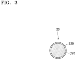
- FIG. 3 is a cross-sectional view illustrating a self-healing capsule (e.g., capsule for self-healing) 20 that may be added to an anisotropic conductive material according to example embodiments.
- a self-healing capsule e.g., capsule for self-healing
- One or more self-healing capsules 20 may be dispersed and used in the matrix material layer 100 of FIG. 1 .
- the anisotropic conductive material may include a plurality of particles 10 and at least one self-healing capsule 20 in the matrix material layer 100. At least one of the particles 10 may be replaced by the particle 11 of FIG. 2 .
- the self-healing capsule 20 may include a core portion C20 and a shell portion S20 covering the core portion C20.
- the core portion C20 may include a self-healing material.
- the self-healing material of the core portion C20 may include an underfill material used in a semiconductor package process.
- the underfill material may be the same as or similar to the material of the matrix material layer 100 of FIG. 1 .
- the underfill material may include a thermosetting resin, a thermoplastic resin, and/or a UV-curable resin.
- the shell portion S20 may include a polymer and/or a ceramic. The materials and properties of the shell portion S20 may be identical or similar to those of the shell portion S10 described with reference to FIG. 1 .
- a package bonding portion (bonding layer) formed by using the anisotropic conductive material including one or more self-healing capsules 20 may have a self-healing function.
- the package bonding portion may be self-healed or self-restored. This will be described later in more detail with reference to FIG. 16 .
- FIG. 1 illustrates the case where the particles 10 are dispersed (or distributed) uniformly or relatively uniformly in the matrix material layer 100.
- the particles 10 may be distributed (or dispersed) non-uniformly in the matrix material layer 100.
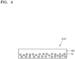
- An example thereof is illustrated in FIG. 4 .
- an anisotropic conductive material A10' may include a matrix material layer 100 and a plurality of particles 10 distributed (or dispersed) in the matrix material layer 100.
- the particles 10 may be distributed at different densities according to regions in the thickness direction of the matrix material layer 100.
- the particles 10 may be dispersed uniformly or relatively uniformly in a lower region of the matrix material layer 100, and the particles 10 may not be present or may be dispersed at a low density in an upper region of the matrix material layer 100.
- the distributions of the particles 10 described herein are merely examples and may vary according to example embodiments.
- the configurations and materials of the particle 10 and the matrix material layer 100 may be identical or similar to those described with reference to FIG. 1 .
- the volume ratio of the particles 10 in the anisotropic conductive materials A10 and A10' of FIGS. 1 and 4 may be less than about 10 vol%.
- the volume ratio of the particles 10 in the anisotropic conductive materials A10 and A10' may be less than or equal to about 7 vol%, or less than or equal to about 5 vol%.
- the content of the particles 10 may be adjusted properly according to the process condition and/or the structure of a bonding target object.
- the anisotropic conductive materials A10 and A10' of FIGS. 1 and 4 may have a kind of film shape.
- the anisotropic conductive materials A10 and A10' of FIGS. 1 and 4 may be an anisotropic conductive film (ACF).
- ACF anisotropic conductive film
- a release layer and a support layer may be provided on one side of the anisotropic conductive material (anisotropic conductive film) A10 or A10'. An example thereof is illustrated in FIG. 5 .
- an anisotropic conductive film A11 may be supported by a support layer SL1, and a release layer RL1 may be provided between the support layer SL1 and the anisotropic conductive film A11.
- the anisotropic conductive film A11 may be easily separated from the support layer SL1 by the release layer RL1.
- the anisotropic conductive film A11 may have an identical or similar configuration to the anisotropic conductive material A10 of FIG. 1 .
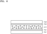
- a release layer RL1 and a support layer SL1 may be provided on both sides of an anisotropic conductive film A11. An example thereof is illustrated in FIG. 6 .
- a first support layer SL1 may be provided on a bottom surface of an anisotropic conductive film A11, and a first release layer RL1 may be provided between the first support layer SL1 and the anisotropic conductive film A11.
- a second support layer SL2 may be provided on a top surface of the anisotropic conductive film A11, and a second release layer RL2 may be provided between the second support layer SL2 and the anisotropic conductive film A11.
- a second anisotropic conductive film may be provided on the second support layer SL2, and a third release layer may be provided between the second support layer SL2 and the second anisotropic conductive film.
- a multilayer structure including the anisotropic conductive film A11 of FIGS. 5 and 6 may have a tape shape elongating in a certain direction, and it may be rolled and used in a roll shape.
- the anisotropic conductive material may have a paste shape instead of a film shape.
- the anisotropic conductive material e.g., A10 of FIG. 1
- ACP anisotropic conductive paste
- ACF anisotropic conductive film
- ACA anisotropic conductive adhesive
- the particles/capsules 10, 11, and 20 described with reference to FIGS. 1 to 3 may be manufactured by various methods.
- the particles/capsules 10, 11, and 20 may be manufactured by a microencapsulation process. An example thereof is illustrated in FIGS. 7A to 7E .
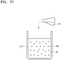
- FIGS. 7A to 7E are diagrams illustrating a method of manufacturing an anisotropic conductive material according to example embodiments.
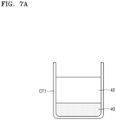
- a conductive liquid material 40 and a solvent material 42 having a different specific gravity from the conductive liquid material 40 may be inserted into a container CT1.
- the specific gravity of the solvent material 42 may be smaller than the specific gravity of the conductive liquid material 40.
- the solvent material 42 may be located above the conductive liquid material 40.
- the conductive liquid material 40 may include, for example, a liquid metal or a molten low melting point solder.
- the liquid metal may include, for example, gallium (Ga), a gallium-indium (Ga-In) alloy, a gallium-indium-tin (Ga-In-Sn) alloy, and/or a gallium-indium-tin-zinc (Ga-In-Sn-Zn) alloy.
- the molten low melting point solder may have a melting point of about 110°C or less (or about 100°C or less) and may include a bismuth-indium (Bi-In)-based alloy, a bismuth-tin (Bi-Sn)-based alloy, an indium-bismuth (In-Bi)-based alloy, a bismuth-indium-tin (Bi-In-Sn)-based alloy, an indium-bismuth-tin (In-Bi-Sn)-based alloy, and/or an indium-tin-zinc (In-Sn-Zn)-based alloy.
- the conductive liquid material 40 may have a configuration including nanofillers (not illustrated).
- the conductive liquid material 40 may include a liquid metal and nanofillers contained in the liquid metal, or may include a suspension having nanofillers dispersed (or distributed) in a solvent instead of a liquid metal.
- the solvent of the suspension may include a different material from the solvent material 42.
- the solvent of the suspension may include ethyl phenylacetate (EPA; C 20 H 30 O 2 ), chlorobenzene (PhCl; C 6 H 5 Cl), and/or hexyl acetate (HA; C 8 H 16 O 2 ).
- the nanofiller may include, for example, one or more conductors from among a carbon nanotube (CNT), a carbon nanofiber (CNF), a carbon black, a fullerene, a graphene flake, a graphene particle, a metal nanowire, and a metal nanoparticle.
- the metal nanowire or the metal nanoparticle may include, for example, metals such as silver (Ag), copper (Cu), and gold (Au).
- the solvent material 42 provided in the container CT1 together with the conductive liquid material 40 may include, for example, water.
- the solvent material 42 is not limited to water and may vary according to example embodiments.
- the solvent material 42 may include any material (liquid) that is not mutually dissolved with the conductive liquid material 40 and has a different specific gravity from the conductive liquid material 40.
- the conductive liquid material 40 and the solvent material 42 may be agitated/stirred by using an agitating/stirring apparatus (not illustrated).
- an ultrasonic wave may be applied to the conductive liquid material 40 and the solvent material 42 by using an ultrasonic generator (not illustrated).
- the conductive liquid material 40 may be divided into a plurality of fine droplets 40c to be dispersed (or distributed) into the solvent material 42.
- the case of performing both the agitation process and the ultrasonic wave application process may reduce the size of the droplet 40c in comparison with the case of performing only the agitation process.
- the agitation process and/or the ultrasonic wave application process may be performed. Also by this method, the intermediate result illustrated in FIG. 7B may be obtained.
- a polymer solution 44 may be provided (dripped or poured) into the solvent material 42 having the fine droplets 40c dispersed therein.
- the polymer solution 44 may be a solution of a polymer material into a solvent, and the solvent of the polymer solution 44 may be selected from among the solvents that are not mutually dissolved with the material of the droplet 40c.
- the surface of the droplet 40c may be coated with the polymer of the polymer solution 44 to form a shell portion 44s as illustrated in FIG. 7D .
- the polymer may be physically/chemically adhered to the surface of the droplet 40c. In other words, due to its property, the polymer may have a relatively great affinity with respect to the surface of the droplet 40c.
- the droplet 40c and the shell portion 44s covering the droplet 40c may be formed into a particle (capsule) P1.
- the droplet 40c of each particle P1 dispersed in the solvent material 42 may be referred to as a "core portion" surrounded by the shell portion 44s.
- a cooling process or an aging process may be further performed to harden/consolidate the shell portion 44s. In this case, a portion of the droplet (core portion) 40c may be hardened to a certain degree.
- a plurality of particles P1 may be separated from the solvent material 42.
- the particles P1 may be separated from the solvent material 42 by a method such as filtration or centrifugation.
- a drying process may be performed on the separated particles P1. Through the drying process, the solvent remaining on/in the shell portion 44s may be vaporized or volatized.
- the particles P1 may be dispersed (or distributed) into a matrix material layer 46 to form an anisotropic conductive material.
- the particles P1 may be dispersed into a polymer resin, a substrate may be coated with the polymer resin having the particles P1 dispersed therein, and then the resulting structure may be dried to form the anisotropic conductive material including the particles P1 dispersed in the matrix material layer 46.
- various factors may affect the control of the size (diameter) of the particle P1.
- the speed of the agitation process agitation speed
- the intensity of the ultrasonic wave application process ultrasonic wave intensity
- the temperature of the container CT1 the temperature of the solvent material 42
- the temperature of the conductive liquid material 40 the pH of the solvent material 42
- the pH of the conductive liquid material 40 may affect the size of the formed droplet 40c and thus may affect the size of the particle P1.
- the size of the formed particle P1 may be easily controlled by controlling various process conditions.
- the particles (capsules) 10, 11, and 20 described with reference to FIGS. 1 to 3 may be formed according to the types of starting materials used in the method of FIGS. 7A to 7E .
- the core portion (droplet) 40c of the formed particle P1 may include the liquid metal.
- the core portion (droplet) 40c of the formed particle P1 may include the nanofillers.
- the conductive liquid material 40 includes the molten low melting point solder in the operation of FIG.
- the core portion (droplet) 40c of the formed particle P1 may include the low melting point solder.
- the core portion (droplet) 40c of the formed particle P1 may include the underfill material.
- FIGS. 7A to 7E illustrate the method of forming the particles (capsules) P1 by the microencapsulation process and the method of the anisotropic conductive material by using the same.
- a plurality of particles (capsules) may be formed by various methods such as a spray drying process, a dripping process, a microemulsion process, a coacervation process, and an interfacial polymerization process, and an anisotropic conductive material according to example embodiments may be manufactured by using the same.
- FIGS. 8A to 8C are cross-sectional views illustrating a method of manufacturing an electronic device by using an anisotropic conductive material according to example embodiments.
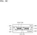
- a first member M10 including one or more first electrode portions E10 may be prepared.
- the first electrode portions E10 may be provided on one side of the first member M10.
- a second member M20 including one or more second electrode portions E20 may be prepared.
- the second electrode portions E20 may be provided on one side of the second member M20.
- the first electrode portion E10 and the second electrode portion E20 may include a kind of pad or bump or any similar element.
- the first electrode portion E10 and the second electrode portion E20 may include, for example, a metal compound or metals such as Au, Cu, and Ag.
- the first member M10 may include, for example, a substrate or a panel.
- the second member M20 may include, for example, a semiconductor chip or a semiconductor chip package.
- the first member M10 will be referred to as "substrate” and the second member M20 will be referred to as "chip”; however, this is merely an example and may vary according to example embodiments.
- an anisotropic conductive material A15 may be provided between the first member M10 and the second member M20.
- the anisotropic conductive material A15 may be provided on the first member M10 to cover the first electrode portions E10, and the second member M20 may be located on/above the anisotropic conductive material A15.
- the second electrode portions E20 of the second member M20 may be arranged to face the first electrode portions E10 of the first member M10.
- the anisotropic conductive material A15 may have an identical or similar configuration to the anisotropic conductive materials A10 and A10' described with reference to FIGS. 1 to 4 .
- the anisotropic conductive material A15 may include a matrix material layer 150 and a plurality of particles 15 dispersed in the matrix material layer 150.
- the particles 15 may include a conductive core portion C15 and an insulating shell portion S15 covering the conductive core portion C15.
- the materials, properties, and/or sizes (diameters/thicknesses) of the core portion C15 and the shell portion S15 may be identical or similar to those of the core portions C10 and C11 and the shell portions S10 and S11 described with reference to FIGS. 1 and 2 .
- the content, distribution, size, and/or particle size distribution of the particles 15 contained in the anisotropic conductive material A15 may be controlled properly according to example embodiments.
- the first member M10 and the second member M20 may be pressed (pressurized) with the anisotropic conductive material A15 therebetween.
- a heating process may be performed to heat the anisotropic conductive material A15 to a certain temperature.
- the insulating shell portion S15 of the particle(s) 15 located between the first electrode portion E10 and the second electrode portion E20 corresponding thereto may be broken and the conductive core portion C15 may be outflowed to electrically connect the first and second electrode portions E10 and E20.
- FIG. 8C A result thereof is illustrated in FIG. 8C .
- the outflowed core portion C15a may be present between the first electrode portion E10 and the second electrode portion E20 corresponding thereto, and the first electrode portion E10 and the second electrode portion E20 corresponding thereto may be electrically connected by the outflowed core portion C15a.
- an intermetallic compound N15a may be formed between the outflowed core portion C15a and the first electrode portion E10 and/or between the outflowed core portion C15a and the second electrode portion E20.
- the intermetallic compound N15a may be formed both between the outflowed core portion C15a and the first electrode portion E10 and between the outflowed core portion C15a and the second electrode portion E20.
- the intermetallic compound N15a may be formed by a reaction between the outflowed core portion C15a and the electrode portion E10/E20.
- the first electrode portion E10 includes Au and the outflowed core portion C15a includes Ga
- AuGa 2 may be formed as the intermetallic compound N15a by the reaction therebetween.
- the intermetallic compound N15a may be formed by the reaction between the In or Sn of the outflowed core portion C15a and the Au, Cu, or Ag of the first electrode portion E10.
- the materials of the formed intermetallic compound N15a may vary according to the materials of the outflowed core portion C15a and the materials of the first electrode portion E10 or the second electrode portion E20.
- the intermetallic compound N15a may be formed by the reaction between the metallic material of the nanofiller and the first electrode portion E10 and/or the second electrode portion E20.
- the outflowed core portion C15a includes a solvent such as EPA, PhCl, or HA
- a solvent such as EPA, PhCl, or HA
- a hardening process may be performed to harden the matrix material layer 150.
- the hardening process may be performed by using heat and/or ultraviolet light.
- the hardening process may be performed as a separate process after the operation of FIG. 8C .
- the matrix material layer 150 may be hardened in the operation of FIG. 8B or 8C .
- the shell portion S15 of the particle 15 may be broken at a relatively-low pressure, the pressure of the pressing process (bonding pressure) used in the operation of FIG. 8B may be reduced.
- the shell portion S15 when the shell portion S15 is formed of a polymer having a low elastic modulus and the thickness of the shell portion S15 is properly controlled, the shell portion S15 may be broken by a considerably-low process pressure (bonding pressure).
- bonding pressure When the anisotropic conductive film (ACF) of the related art is used, a bonding pressure of about 30 MPa or more, for example, about 30 MPa to about 100 MPa may be required.
- the bonding (connecting) process may be performed even by a low bonding pressure corresponding to about 1/2 or less, for example, about 1/5 of the bonding pressure of the related art.
- the first electrode portion E10 and the second electrode portion E20 may be electrically connected by a pressure in a range of about 0 MPa to less than about 30 MPa, by a low pressure in a range of about 0 MPa to about 10 MPa or less, or by a lower pressure in a range of about 0 MPa to about 3 MPa or less.
- the bonding (connecting) process since the bonding (connecting) process may be performed by a low pressure, the problems caused by a high pressure may be suppressed or prevented and the process load and cost may be reduced.
- the bonding process when the bonding process is performed by a relatively-high pressure as in the related art, the substrate (first member M10) or the chip (second member M20) may be damaged and the reliability of the manufactured device may be degraded.
- the bonding (connecting) process since the bonding (connecting) process may be performed by a considerably-low pressure in comparison with the related art, the problems caused by a high pressure may be suppressed or prevented and the device having excellent reliability may be manufactured.
- the bonding pressure used in example embodiments may not necessarily be lower than about 30 MPa. Depending on the thickness and material of the shell portion S15, the pressure for the bonding (connecting) process may be higher than about 30 MPa.
- the temperature of the heating process used in the bonding (connecting) process may be reduced.
- the temperature of the heading process (bonding temperature) used in the operation of FIG. 8B may be reduced.
- the bonding (connecting) process may be performed at a temperature of about 110°C or less.
- the bonding (connecting) process may be performed at a room temperature without the heating process.
- the intermetallic compound N15a may also be formed at a room temperature.
- the bonding (connecting) process may be performed at a temperature corresponding to the melting point of the low melting point solder or at a temperature higher than the melting point of the low melting point solder. Even in this case, the used temperature (bonding temperature) may be about 110°C or less (or about 100°C or less).
- the anisotropic conductive film (ACF) of the related art is used, a bonding temperature of about 150°C or more may be required to obtain a desired level of contact resistance.
- the process temperature (bonding temperature) may be reduced by about 50°C or more or by about 80°C or more in comparison with the related art.
- the problems caused by the high process temperature (bonding temperature) may be suppressed or prevented, and the process load and the manufacturing cost may be reduced.
- the problem of a bonding alignment distortion may be suppressed or prevented, the device reliability may be improved. If the bonding (connecting) process is performed at a room temperature without the heating process, the problems caused by the high-temperature heating process may be fundamentally limited (and/or prevented).
- a relatively-large contact area may be formed between the outflowed core portions C15a and the first and second electrode portions E10 and E20.
- the contact area between the outflowed core portion C15a and the first core portion E10 or the second electrode portion E20 may be about 0.75 ⁇ m 2 or more or about 1 ⁇ m 2 or more.
- the contact area may include both the indirect contact with the intermetallic compound N15a therebetween and the direct contact without the intermetallic compound N15a therebetween.
- the liquid material of the core portion C15 may be outflowed to form a relatively-large contact area with the first and second electrode portions E10 and E20, an excellent contact property and a low contact resistance may be ensured.
- the intermetallic compound N15a when the intermetallic compound N15a is formed between the outflowed core portion C15a and the first and second electrode portions E10 and E20, the contact resistance may be further reduced and the contact property may be further improved by the intermetallic compound N15a.
- the intermetallic compound N15a may be formed at a room temperature or a temperature of about 110°C or less.
- the outflowed core portion C15a between the first electrode portion E10 and the second electrode portion E20 corresponding thereto may maintain the position within the gap between the first electrode portion E10 and the second electrode portion E20. Since the distance between the first electrode portion E10 and the second electrode portion E20 corresponding thereto is relatively small and the matrix material layer 150 is present around the outflowed core portion C15a, the outflowed core portion C15a may identically or substantially maintain the original position without deviating from the gap therebetween.
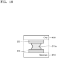
- FIG. 9 illustrates an example of an electronic device according to example embodiments, which may correspond to an enlarged view of the principal part of FIG. 8C .
- the outflowed core portion C15a may be present between the first and second electrode portions E10 and E20, and the intermetallic compound N15a may not be formed unlike the illustration of FIG. 9 .
- the intermetallic compound (N15a of FIG. 9 ) may not be formed.
- FIG. 11 is a cross-sectional view illustrating an electronic device manufactured by using an anisotropic conductive film A1 according to a comparative example.
- the anisotropic conductive film A1 according to the comparative example may include a conductive ball 1.
- the conductive ball 1 may include an insulating polymer bead b1 and a conductive metal coating film m1 covering the insulating polymer bead b1. Since the particle (e.g., 15 of FIG. 8A ) according to example embodiments includes the conductive core portion C15 and the insulating shell portion S15 covering the conductive core portion C15, the conductive ball 1 according to the comparative example may be said to have an opposite structure to the particle according to example embodiments.
- first and second electrode portions E1 and E2 may be electrically connected by the conductive metal coating film m1.
- the conductive ball 1 is strained to some degree by receiving a pressure between the first and second electrode portions E1 and E2, a certain degree of contact area may be ensured and the first and second electrode portions E1 and E2 may be electrically connected to each other.
- a bonding temperature of about 150°C or more and a bonding pressure of at least about 30 MPa or more may be required to reduce the contact resistance.
- both a relatively-high bonding temperature and a relatively-high bonding pressure may be required.
- various problems may be caused by the high bonding temperature and the high bonding pressure.
- the connection between the two electrode portions E1 and E2 by the conductive ball 1 may be referred to as an electrical connection by "simple physical contact".
- the contact between the conductive ball 1 and the electrode portions E1 and E2 may be a narrow-area contact similar to a point contact, and an intermetallic compound may not be formed therebetween. Thus, it may be difficult to ensure an excellent contact property and a low contact resistance.
- the bonding temperature and the bonding pressure may be reduced considerably in comparison with the related art, and the excellent contact property and the low contact resistance may be easily ensured.
- the electronic device having excellent performance and reliability may be easily manufactured.
- an undesired electrical connection may occur between the adjacent electrode portions E1 and E2.
- a lateral connection may occur instead of a vertical connection.
- the possibility of occurrence of this problem may increase when the distance (pitch) between the first electrode portions E1 and the distance (pitch) between the second electrode portions E2 are small.
- the possibility of occurrence of the short problem as in FIG. 12 may be high in a device having a fine pitch between electrodes.
- the first member M1 may be deformed (strained) and thus the bonding alignment may be distorted. This problem may occur when using a substrate (first member M1) that may be easily deformed (stained) by a bonding process temperature of about 150°C or more or by a bonding process pressure of about 30 MPa or more.
- FIGS. 12 and 13 may occur separately or in combination, and these problems may cause the increase of the error rate of the electronic device.
- FIG. 14 is a diagram illustrating a short problem caused by the conductive ball 1 used in the anisotropic conductive film according to a comparative example.
- the conductive ball (particle) 1 since the conductive ball (particle) 1 includes the insulating polymer bead b1 and the conductive metal coating film m1 covering the insulating polymer bead b1, when a plurality of conductive balls (particles) 1 contact each other, an electrical connection may easily occur between the particles. When the electrical connection between the particles occurs between the adjacent electrode portions E1 and E2 of FIG. 12 , an undesired electrical connection (short) may occur.
- anisotropic conductive material may limit and/or prevent the problem illustrated in FIG. 14 . This will be described below with reference to FIG. 15 .
- a particle (capsule) 15 used in an anisotropic conductive material may include a conductive core portion C15 and an insulating shell portion S15 covering the conductive core portion C15.
- an electrical connection between the particles is limited (and/or prevented) by the insulating shell portion S15 and the insulating property thereof may be maintained.
- the short problem illustrated in FIGS. 12 and 14 may be limited (and/or prevented). Therefore, the use of the particles 15 according to example embodiments may limit and/or prevent or suppress the possibility of an error caused by the short when manufacturing the electronic device including electrodes having a fine pitch.
- the anisotropic conductive material including the particles 15 according to example embodiments may be advantageously used to implement the electronic device including electrodes having a fine pitch.
- FIG. 16 is a cross-sectional view illustrating an electronic device manufactured by using an anisotropic conductive material according to example embodiments.
- the anisotropic conductive material A25 of FIG. 16 may further include a self-healing capsule 25.
- the self-healing capsule 25 may be identical to the self-healing capsule 20 described with reference to FIG. 3 .
- the anisotropic conductive material A25 including the self-healing capsule 25 and a plurality of particles 15 in a matrix material layer 250 by using the anisotropic conductive material A25 including the self-healing capsule 25 and a plurality of particles 15 in a matrix material layer 250, a first member M10 and a second member M20 may be adhered to each other, and electrode portions E10 and E20 thereof may be electrically connected to each other.
- the matrix material layer 250 of the anisotropic conductive material A25 may function as both a bonding portion and a support portion.
- the anisotropic conductive material A25 may be referred to as a bonding portion or a support portion.
- a crack may occur at the anisotropic conductive material A25 due to various external factors (e.g., a physical impact, a thermal stress, and/or a substrate strain), and the crack may be propagated to cause a problem such as delamination.
- a self-healing or self-restoring function may be performed to fill the crack with the underfill material that is outflowed from the core portion of the self-healing capsule 25 adjacent to the crack.
- the material of the core portion may be hardened by reacting with a catalyst material that is present in the matrix material layer 250. In this manner, when the self-healing capsule 25 is used, since a possible crack caused by various external factors may be self-healed (self-restored), the bonding reliability thereof may be improved and the durability of the electronic device may be improved.
- Anisotropic conductive materials may be used to manufacture various electronic devices (electronic apparatuses) and semiconductor devices (semiconductor apparatuses).
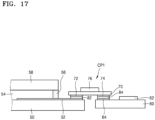
- FIG. 17 is a cross-sectional view illustrating an example of an electronic device including an anisotropic conductive material according to example embodiments.
- the electronic device of example embodiments may include, for example, a display device such as a liquid crystal display (LCD).
- LCD liquid crystal display
- a thin film transistor (TFT) array substrate 50 including a plurality of TFTs may be prepared, and a color filter substrate 58 facing the TFT array substrate 50 may be prepared.
- a liquid crystal layer 54 may be provided between the TFT array substrate 50 and the color filter substrate 58, and a seal 56 may be provided to seal the liquid crystal layer 54.
- a first electrode pad 52 may be prepared on the TFT array substrate 50.
- the first electrode pad 52 may have a structure extending outside the seal 56 from a region in which the liquid crystal layer 54 is formed.
- the above shape and formation range of the first electrode pad 52 are merely examples and may vary according to example embodiments.
- the TFT array substrate 50, the color filter substrate 58, and the liquid crystal layer 54 provided therebetween may be said to constitute a "display panel".
- a printed circuit board (PCB) substrate 60 may be prepared to be spaced apart from the TFT array substrate 50.
- the PCB substrate 60 may include a chip 62.
- the PCB substrate 60 may include a second electrode pad 64.
- a driver integrated circuit (IC) package CP1 may be provided between the TFT array substrate 50 and the PCB substrate 60 to connect the TFT array substrate 50 and the PCB substrate 60 to each other.
- the driver IC package CP1 may include, for example, a driver IC 76 mounted on a carrier tape 70. Also, the driver IC package CP1 may include a first electrode element 72 and a second electrode element 74 that are provided on a bottom surface of the carrier tape 70.
- the driver IC package CP1 may be referred to as a tape carrier package (TCP).
- the first electrode pad 52 and the first electrode element 72 may be electrically connected and bonded to each other by an anisotropic conductive material (anisotropic conductive film) 82 provided therebetween.
- the anisotropic conductive material (anisotropic conductive film) 82 may include one of the above-described anisotropic conductive materials according to example embodiments.
- a bonding layer 84 may be provided between the second electrode pad 64 and the second electrode element 74 to electrically connect the second electrode pad 64 and the second electrode element 74.
- the bonding layer 84 may include a general solder material.
- the bonding layer 84 may be formed by using one of the above-described anisotropic conductive materials according to example embodiments. In the latter case, the bonding layer 84 may have an identical or similar configuration to the anisotropic conductive material (anisotropic conductive film) 82.
- FIG. 17 illustrates an example of an electronic device including an anisotropic conductive material according to example embodiments
- the anisotropic conductive material according to example embodiments may be applied not only to the device of FIG. 17 but also to various other devices.
- the anisotropic conductive material may be applied to various bonding methods such as chip-on-glass (COG) bonding, chip-on-board (COB) bonding, chip-on-film (COF) bonding, and tape-automated bonding (TAB).
- COG chip-on-glass
- COB chip-on-board
- COF chip-on-film
- TAB tape-automated bonding
- the anisotropic conductive material may be applied to various fields such as a process for bonding an integrated circuit (IC) to a liquid crystal display (LCD), a process for bonding a printed circuit board (PCB) to an IC, a process for bonding a flexible printed circuit (FPC) to an IC, a process for bonding an FPC to a plasma display panel (PDP), a process for bonding a tape carrier package (TCP) to an LCD, a process for bonding a TCP to a PCB, a process for bonding an FPC to an LCD, and a process for bonding an FPC to a PCB.
- IC integrated circuit
- PCB printed circuit board
- FPC flexible printed circuit
- TCP tape carrier package
- the anisotropic conductive material may be applied to fields such as plasma displays and flip chip packages.
- the anisotropic conductive material according to example embodiments may be applied to any field to which the anisotropic conductive film and the anisotropic conductive paste of the related art may be applied.
- FIG. 18 is an optical microscope image illustrating a plurality of particles (capsules) formed according to example embodiments.
- the particle (capsule) of FIG. 18 may correspond to the particle 10 of FIG. 1 .
- the particles (capsules) have a substantially-spherical shape or any similar shape and have a diameter (size) of less than tens of ⁇ m.
- the particle (capsule) may have a diameter (size) of about 1 ⁇ m to about 100 ⁇ m or about 5 ⁇ m to about 50 ⁇ m.
- the diameter (size) of the particle (capsule) may be controlled by the process conditions.
- a core portion of the particle (capsule) illustrated in FIG. 18 includes a liquid metal "Ga", and a shell portion thereof includes an insulating polymer.
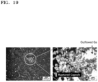
- the particle (capsule) was artificially broken by using a slide glass. The result thereof was the same as illustrated in FIG. 19 (the optical microscope image). Referring to FIG. 19 , it may be seen that the liquid-state Ga is outflowed when the particle (capsule) is broken. A white portion in the right image of FIG. 19 corresponds to Ga.
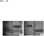
- the particles (capsules) of FIG. 18 were dispersed into a polymer resin (epoxy resin), a blade coating method was used to coat a substrate with the polymer resin (epoxy resin) having the particles (capsules) dispersed therein, and then the resulting structure was dried. Accordingly, an anisotropic conductive film (ACF) including the particles (capsules) dispersed in the polymer resin was formed.
- ACF anisotropic conductive film
- FIG. 20 is an optical microscope image illustrating a result obtained by artificially forming a scratch on the anisotropic conductive film (ACF) formed according to the above method. Referring to FIG. 20 , it may be seen that when an artificial scratch is formed on the anisotropic conductive film (ACF), the particles (capsules) are broken by the scratch and thus the liquid metal (Ga) is outflowed therefrom.
- ACF anisotropic conductive film
- FIG. 21 illustrates a setup for measuring a breaking force of the particle (capsule) according to example embodiments.
- FIG. 22 illustrates the result of measuring a breaking force for each size of the particle (capsule) by using the setup of FIG. 21 .
- the breaking force of particles (capsules) is measured by a digital gauge while applying a pressure thereto.
- the measurement results thereof are illustrated in the graph of FIG. 22 .
- the breaking force thereof when a plurality of particles (capsules) of a first group have a size of about 30 ⁇ m to about 50 ⁇ m, the breaking force thereof is about 2.63 N.
- a plurality of particles (capsules) of a second group have a size of about 5 ⁇ m to about 10 ⁇ m, the breaking force thereof is about 0.57 N.
- the number of the particles (capsules) of the first group is equal to the number of the particles (capsules) of the second group. From this result, it may be seen that the breaking force decreases by about 77% when the size of the particle (capsule) decreases from about 30 ⁇ m to about 50 ⁇ m to about 5 ⁇ m to about 10 ⁇ m. It is expected that the breaking force decrease because the thickness of the shell portion decreases with the decrease of the particle (capsule) size.
- the force used for breaking the particles (capsules) having a size of about 30 ⁇ m to about 50 ⁇ m was measured as about 2.63 N.
- the area occupied by the particles (capsules) when this is converted in units of MPa, it is estimated as about 1 MPa or less.
- This may be a low pressure of at least about 1/5 or less in comparison with the pressure necessary for the bonding process based on the anisotropic conductive film (ACF) of the related art. Accordingly, it is expected that when the anisotropic conductive material (anisotropic conductive film) according to example embodiments is used, the pressure used for the bonding process may be reduced considerably in comparison with the related art.
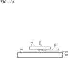
- FIG. 23 illustrates a setup for a current-flowing experiment based on the break of the particle (capsule) according to example embodiments.
- FIG. 24 is a schematic diagram illustrating the setup of FIG. 23 in detail.
- FIG. 25 illustrates the result of measuring a current-flowing force for each size of the particle (capsule) by using the setup of FIG. 23 .
- a disconnected Cu interconnection line 92 is disposed on a glass substrate 90, a plurality of particles (capsules) 94 are loaded on the disconnected portion of the Cu interconnection line 92, an upper glass 96 is disposed thereon, and the force (strength) necessary for flowing a current through the Cu interconnection line 92 by breaking the particle (capsule) is measured while applying a pressure thereon. The measurement results thereof are illustrated in the graph of FIG. 25 .
- the current-flowing force thereof when a plurality of particles (capsules) of a first group have a size of about 30 ⁇ m to about 50 ⁇ m, the current-flowing force thereof is about 4.43 N.
- the current-flowing force thereof is about 2.95 N.
- the number of the particles (capsules) of the first group is equal to the number of the particles (capsules) of the second group. From this result, it may be seen that the current-flowing force decreases by about 34% when the size of the particle (capsule) decreases from about 30 ⁇ m to about 50 ⁇ m to about 5 ⁇ m to about 10 ⁇ m. Since a conductive material is outflowed by the break of the particle (capsule), an electrical connection therebetween may be formed through the outflowed conductive material. Also, as the size of the particle (capsule) decreases, the breaking force for the electrical connection may decrease.
- anisotropic conductive material may be used not only in the display device of FIG. 17 but also in various semiconductor device mounting technologies and may also be applied to the field of chip-to-chip connection in some cases. Therefore, the scope of inventive concepts should be defined not by only the example embodiments herein but by the technical scope described in the following claims.
Landscapes
- Engineering & Computer Science (AREA)
- Physics & Mathematics (AREA)
- Chemical & Material Sciences (AREA)
- Dispersion Chemistry (AREA)
- Spectroscopy & Molecular Physics (AREA)
- Microelectronics & Electronic Packaging (AREA)
- Manufacturing & Machinery (AREA)
- Power Engineering (AREA)
- Computer Hardware Design (AREA)
- Conductive Materials (AREA)
- General Physics & Mathematics (AREA)
- Condensed Matter Physics & Semiconductors (AREA)
- Non-Insulated Conductors (AREA)
- Wire Bonding (AREA)
- Powder Metallurgy (AREA)
- Crystallography & Structural Chemistry (AREA)
- Nanotechnology (AREA)
- Organic Chemistry (AREA)
Applications Claiming Priority (1)
| Application Number | Priority Date | Filing Date | Title |
|---|---|---|---|
| KR1020150123207A KR102429873B1 (ko) | 2015-08-31 | 2015-08-31 | 이방성 도전 재료와 이방성 도전 재료를 포함하는 전자소자 및 그 제조방법 |
Publications (2)
| Publication Number | Publication Date |
|---|---|
| EP3142124A1 EP3142124A1 (en) | 2017-03-15 |
| EP3142124B1 true EP3142124B1 (en) | 2023-05-31 |
Family
ID=56024102
Family Applications (1)
| Application Number | Title | Priority Date | Filing Date |
|---|---|---|---|
| EP16167463.5A Active EP3142124B1 (en) | 2015-08-31 | 2016-04-28 | Anisotropic conductive material and an electronic device including anisotropic conductive material |
Country Status (5)
| Country | Link |
|---|---|
| US (1) | US9831211B2 (ja) |
| EP (1) | EP3142124B1 (ja) |
| JP (1) | JP6723552B2 (ja) |
| KR (1) | KR102429873B1 (ja) |
| CN (1) | CN106486183B (ja) |
Families Citing this family (48)
| Publication number | Priority date | Publication date | Assignee | Title |
|---|---|---|---|---|
| DE102015220435A1 (de) * | 2015-10-20 | 2017-04-20 | Continental Reifen Deutschland Gmbh | Faden und Fahrzeugluftreifen |
| KR102675774B1 (ko) * | 2016-11-30 | 2024-06-18 | 삼성전자주식회사 | 페이스트 재료와 이로부터 형성된 배선 부재 및 배선 부재를 포함하는 전자소자 |
| JP6792788B2 (ja) * | 2017-03-30 | 2020-12-02 | 東京エレクトロン株式会社 | 半導体装置の製造方法 |
| US10750623B2 (en) * | 2017-05-12 | 2020-08-18 | International Business Machines Corporation | Forming conductive vias using healing layer |
| KR101993812B1 (ko) * | 2017-12-11 | 2019-06-27 | 울산과학기술원 | 상온 액체금속 캡슐 및 그 제조 방법 |
| KR101993813B1 (ko) * | 2017-12-11 | 2019-06-27 | 울산과학기술원 | 상온 액체금속 캡슐 잉크, 그 제조 방법, 및 이를 이용하여 형성한 상온 액체금속 캡슐 배선 |
| CN111971264A (zh) * | 2017-12-14 | 2020-11-20 | 百可悠有限公司 | 异向性奈米粒子的组成与方法 |
| CN108110261B (zh) * | 2017-12-29 | 2018-11-30 | 成都新柯力化工科技有限公司 | 一种燃料电池用金属粒子-液态金属催化剂及制备方法 |
| KR101964881B1 (ko) * | 2018-01-17 | 2019-04-02 | 울산과학기술원 | 상온 액체 금속 캡슐을 이용하여 디바이스를 치유하는 신축성 패키지 및 이의 제조방법 |
| JP7100980B2 (ja) | 2018-01-22 | 2022-07-14 | ローム株式会社 | Ledパッケージ |
| TWI904579B (zh) | 2018-06-26 | 2025-11-11 | 日商力森諾科股份有限公司 | 焊料粒 |
| CN112313032A (zh) | 2018-06-26 | 2021-02-02 | 昭和电工材料株式会社 | 各向异性导电膜及其制造方法以及连接结构体的制造方法 |
| CN108928056B (zh) * | 2018-08-01 | 2020-06-05 | 京东方科技集团股份有限公司 | 膜材及其制备方法、显示基板 |
| US10800948B2 (en) * | 2018-08-02 | 2020-10-13 | Xerox Corporation | Conductive adhesive compositions and method for the same |
| DE102018215541A1 (de) * | 2018-09-12 | 2020-03-12 | Bayerische Motoren Werke Aktiengesellschaft | Selbstheilende elektrische Leitung |
| CN109143699A (zh) * | 2018-10-08 | 2019-01-04 | 惠科股份有限公司 | 一种显示面板及其制造方法和显示装置 |
| US10818634B2 (en) | 2018-10-08 | 2020-10-27 | HKC Corporation Limited | Display panel, method for manufacturing the display panel, and display device |
| US20210240095A1 (en) * | 2018-11-01 | 2021-08-05 | Hewlett-Packard Development Company, L.P. | Electrophotographic ink compositions |
| CN109852281B (zh) * | 2019-02-01 | 2020-07-28 | 扬州富威尔复合材料有限公司 | 一种基于液态金属的各向异性导电胶的制备方法 |
| CN109822256B (zh) * | 2019-03-15 | 2021-08-06 | 南昌大学 | 一种低熔点In-Sn-Bi合金钎料及制备方法 |
| KR102113732B1 (ko) * | 2019-03-21 | 2020-05-21 | 주식회사 아이에스시 | 도전성 분말 및 이를 포함하는 검사용 커넥터 |
| CN112349447B (zh) * | 2019-08-06 | 2022-04-12 | 北京梦之墨科技有限公司 | 一种导电材料及其制备方法、电子器件 |
| JP7363918B2 (ja) * | 2019-11-20 | 2023-10-18 | 日産化学株式会社 | 異方性導電材料 |
| CN110729071B (zh) * | 2019-12-19 | 2020-06-09 | 北京梦之墨科技有限公司 | 液态金属导电浆料及电子器件 |
| KR102754472B1 (ko) * | 2019-12-23 | 2025-01-17 | 엘지디스플레이 주식회사 | 자성 도전볼을 포함하는 이방성 도전 필름 및 이를 이용한 표시 장치 |
| CN111192705B (zh) * | 2020-01-07 | 2021-07-02 | 北京梦之墨科技有限公司 | 一种液态金属导电浆料、电子器件及其制作方法 |
| CN113539547B (zh) * | 2020-04-17 | 2024-02-23 | 北京梦之墨科技有限公司 | 一种柔性导电浆料及柔性电子器件 |
| US11543322B2 (en) * | 2020-05-01 | 2023-01-03 | Globalfoundries U.S. Inc. | Crack identification in IC chip package using encapsulated liquid penetrant contrast agent |
| CN111813263B (zh) * | 2020-07-10 | 2022-09-20 | 业成科技(成都)有限公司 | 热塑成形的修复粒子及方法 |
| US12030126B2 (en) * | 2020-07-24 | 2024-07-09 | The Indium Corporation Of America | Undercooled liquid metallic droplets having a protective shell |
| KR102818103B1 (ko) | 2020-08-03 | 2025-06-11 | 삼성전자주식회사 | 열 전달 물질 및 그 제조 방법과 이를 포함하는 반도체 패키지 |
| JP7080939B2 (ja) * | 2020-09-04 | 2022-06-06 | 株式会社新菱 | 低融点接合部材およびその製造方法ならびに半導体電子回路およびその実装方法 |
| DE102020124955B4 (de) * | 2020-09-24 | 2025-04-03 | Cosa Group Gmbh | Elektronikeinheit mit einem integrierten Schaltkreis und Verfahren zu deren Herstellung |
| TWI745167B (zh) * | 2020-11-17 | 2021-11-01 | 財團法人金屬工業研究發展中心 | 具有修復微粒的自癒性金屬材料及其製造方法 |
| CN114724741B (zh) * | 2021-01-06 | 2022-12-30 | 北京梦之墨科技有限公司 | 液态金属微胶囊、导电浆料及其制备方法、电子器件 |
| CN113285288B (zh) * | 2021-04-25 | 2023-05-02 | 吴江市联祥电子有限公司 | 一种裂缝自填充式电子连接器及其加工工艺 |
| KR20220154545A (ko) | 2021-05-13 | 2022-11-22 | 엘지디스플레이 주식회사 | 액체 금속을 포함하는 이방성 도전 필름, 그 제조방법 및 이를 이용한 표시장치 |
| US11633702B2 (en) | 2021-07-07 | 2023-04-25 | SAFI-Tech, Inc. | Solder paste on demand apparatus |
| CN113990557B (zh) * | 2021-09-09 | 2024-03-29 | 山西聚微天成科技有限公司 | 一种高导电性和高拉伸性弹性体的制备方法及其应用 |
| JP7777331B2 (ja) * | 2021-11-15 | 2025-11-28 | 株式会社ケムソル | 異方性導電フィルム並びにそれを用いた接合方法及び接合体 |
| JP2025518499A (ja) * | 2022-05-09 | 2025-06-17 | マイダス エイチアンドティー インコーポレイテッド | 液体金属粒子を含む異方伝導性弾性素材及びその製造方法 |
| KR102659446B1 (ko) * | 2022-06-22 | 2024-04-23 | 경희대학교 산학협력단 | 자가치유 가능한 전극 및 이의 제조방법 |
| CN115206588B (zh) * | 2022-07-20 | 2023-04-07 | 南平市延平鑫东来科技有限公司 | 一种导电剂及其制备方法和在碱锰电池中的应用 |
| CN115340803A (zh) * | 2022-08-19 | 2022-11-15 | 元旭半导体科技(无锡)有限公司 | 导电涂覆材料及制备方法,显示面板及封装方法 |
| DE102022124574A1 (de) * | 2022-09-23 | 2024-03-28 | Ams-Osram International Gmbh | Verfahren zum herstellen eines elektronischen bauelements und elektronisches bauelement |
| DE102022130878A1 (de) * | 2022-11-22 | 2024-05-23 | Ams-Osram International Gmbh | Verfahren zum herstellen eines elektronischen bauelements |
| CN116033777A (zh) * | 2023-02-01 | 2023-04-28 | 固安翌光科技有限公司 | 一种oled器件的隔离元件、层间结构及oled器件 |
| CN120568612B (zh) * | 2025-04-25 | 2025-12-02 | 广东工业大学 | 基于液流自组装定位的精细线路修复方法、系统及线路板 |
Citations (2)
| Publication number | Priority date | Publication date | Assignee | Title |
|---|---|---|---|---|
| US20070063347A1 (en) * | 2005-09-19 | 2007-03-22 | Taiwan Semiconductor Manufacturing Co., Ltd. | Packages, anisotropic conductive films, and conductive particles utilized therein |
| US20140299231A1 (en) * | 2013-04-05 | 2014-10-09 | Samsung Electronics Co., Ltd. | Metal-based solder composite including conductive self-healing materials |
Family Cites Families (23)
| Publication number | Priority date | Publication date | Assignee | Title |
|---|---|---|---|---|
| US5445308A (en) * | 1993-03-29 | 1995-08-29 | Nelson; Richard D. | Thermally conductive connection with matrix material and randomly dispersed filler containing liquid metal |
| JPH08311420A (ja) | 1995-05-24 | 1996-11-26 | Sony Corp | 異方性導電膜 |
| US6339120B1 (en) | 2000-04-05 | 2002-01-15 | The Bergquist Company | Method of preparing thermally conductive compounds by liquid metal bridged particle clusters |
| JP2004331910A (ja) * | 2003-05-12 | 2004-11-25 | Seiko Epson Corp | 異方導電性接着剤、実装方法、電気光学装置モジュールおよび電子機器 |
| US20050228097A1 (en) | 2004-03-30 | 2005-10-13 | General Electric Company | Thermally conductive compositions and methods of making thereof |
| JP2006206833A (ja) * | 2005-01-31 | 2006-08-10 | Toshiba Matsushita Display Technology Co Ltd | 異方導電性接着剤及びこれを用いた接続構造、接続方法 |
| GB2426010B (en) * | 2005-05-14 | 2011-04-06 | Jeffrey Boardman | semiconductor materials and methods of producing them |
| JP2007165028A (ja) | 2005-12-12 | 2007-06-28 | Matsushita Electric Ind Co Ltd | 異方導電性材料とこれを用いた実装方法 |
| KR100874540B1 (ko) * | 2007-05-03 | 2008-12-16 | 엘에스엠트론 주식회사 | 이방 도전성 접착 캡슐 |
| US9208931B2 (en) | 2008-09-30 | 2015-12-08 | Littelfuse, Inc. | Voltage switchable dielectric material containing conductor-on-conductor core shelled particles |
| JP5075180B2 (ja) | 2009-03-31 | 2012-11-14 | コリア・インスティテュート・オブ・サイエンス・アンド・テクノロジー | 導電性粒子及びこれを含む異方性導電フィルム |
| KR101090106B1 (ko) | 2009-05-26 | 2011-12-07 | 한국과학기술연구원 | 전기 전도성 입자 및 그 제조 방법 |
| KR101239371B1 (ko) | 2011-04-01 | 2013-03-18 | 한국과학기술연구원 | 도전성 입자 및 그의 제조방법 |
| JP5650611B2 (ja) | 2011-08-23 | 2015-01-07 | デクセリアルズ株式会社 | 異方性導電フィルム、異方性導電フィルムの製造方法、接続方法、及び接合体 |
| KR101168038B1 (ko) | 2011-12-15 | 2012-07-27 | 한국건설생활환경시험연구원 | 마이크로캡슐, 자기치유 코팅재 형성용 조성물, 및 캡슐 분산형 자기치유 코팅재와 그의 제조방법 |
| CN103013370B (zh) | 2012-12-14 | 2014-12-10 | 京东方科技集团股份有限公司 | 一种各向异性导电胶膜及电子装置 |
| KR20140139902A (ko) | 2013-05-28 | 2014-12-08 | 삼성디스플레이 주식회사 | 이방성 도전 필름 적층체, 이를 포함하는 표시 장치 및 표시 장치 제조 방법 |
| KR101659128B1 (ko) | 2013-09-30 | 2016-09-22 | 제일모직주식회사 | 이방성 도전 필름 및 이를 이용한 반도체 장치 |
| JP2015076486A (ja) | 2013-10-08 | 2015-04-20 | 株式会社ジャパンディスプレイ | 表示装置 |
| US10032538B2 (en) | 2013-11-13 | 2018-07-24 | The United States Of America As Represented By The Secretary Of The Army | Deformable elastomeric conductors and differential electronic signal transmission |
| CN203707402U (zh) * | 2013-12-05 | 2014-07-09 | 番禺得意精密电子工业有限公司 | 电连接器 |
| KR102237786B1 (ko) * | 2014-01-02 | 2021-04-09 | 삼성디스플레이 주식회사 | 실런트 조성물, 실런트 조성물의 제조 방법 및 실런트를 포함하는 표시 패널 |
| CN104028184B (zh) * | 2014-06-21 | 2016-02-03 | 电子科技大学 | 一种反应性液态芯材的导电聚合物微胶囊及其制备方法 |
-
2015
- 2015-08-31 KR KR1020150123207A patent/KR102429873B1/ko active Active
-
2016
- 2016-02-04 US US15/015,758 patent/US9831211B2/en active Active
- 2016-04-28 EP EP16167463.5A patent/EP3142124B1/en active Active
- 2016-05-10 CN CN201610306096.3A patent/CN106486183B/zh active Active
- 2016-05-24 JP JP2016103093A patent/JP6723552B2/ja active Active
Patent Citations (2)
| Publication number | Priority date | Publication date | Assignee | Title |
|---|---|---|---|---|
| US20070063347A1 (en) * | 2005-09-19 | 2007-03-22 | Taiwan Semiconductor Manufacturing Co., Ltd. | Packages, anisotropic conductive films, and conductive particles utilized therein |
| US20140299231A1 (en) * | 2013-04-05 | 2014-10-09 | Samsung Electronics Co., Ltd. | Metal-based solder composite including conductive self-healing materials |
Also Published As
| Publication number | Publication date |
|---|---|
| CN106486183A (zh) | 2017-03-08 |
| JP2017050273A (ja) | 2017-03-09 |
| EP3142124A1 (en) | 2017-03-15 |
| CN106486183B (zh) | 2020-06-30 |
| JP6723552B2 (ja) | 2020-07-15 |
| KR20170025996A (ko) | 2017-03-08 |
| US9831211B2 (en) | 2017-11-28 |
| US20170062374A1 (en) | 2017-03-02 |
| KR102429873B1 (ko) | 2022-08-05 |
Similar Documents
| Publication | Publication Date | Title |
|---|---|---|
| EP3142124B1 (en) | Anisotropic conductive material and an electronic device including anisotropic conductive material | |
| CN101432931B (zh) | 导电颗粒配置薄片及各向异性导电膜 | |
| US7081675B2 (en) | Multilayered anisotropic conductive adhesive for fine pitch | |
| CN103178033B (zh) | 由包括导电微球的各向异性导电膜连接的半导体装置 | |
| CN104106182B (zh) | 各向异性导电连接材料、连接结构体、连接结构体的制造方法和连接方法 | |
| US20030008133A1 (en) | Anisotropic conductive film and method of fabricating the same for ultra-fine pitch COG application | |
| JP2002501821A (ja) | 粒子の非ランダム単層にコーティングを形成する方法、及びそれによって形成された製品 | |
| CN106939146A (zh) | 各向异性导电膜及其制法、连接体及其制法以及连接方法 | |
| TWI548718B (zh) | A circuit-connecting material, and a method of manufacturing the same | |
| CN105917529A (zh) | 连接体、连接体的制造方法、连接方法、各向异性导电粘接剂 | |
| WO2015091673A1 (en) | Bonded assemblies with pre-deposited polymer balls on demarcated areas and methods of forming such bonded assemblies | |
| TWI775562B (zh) | 異向性導電膜之製造方法、異向性導電膜、異向性導電膜捲裝體、連接構造體之製造方法、連接構造體、填料配置膜之製造方法、及填料配置膜 | |
| CN110619817A (zh) | 异方性导电胶、显示面板及基板的绑定方法 | |
| Lu et al. | Electrically conductive adhesives (ECAs) | |
| US20160126202A1 (en) | Bridging arrangement, microelectronic component and method for manufacturing a bridging arrangement | |
| CN102290127A (zh) | 异方性导电膜及其制造方法 | |
| JP2004006417A (ja) | 接続部材及びこれを用いた電極の接続構造 | |
| JP4670859B2 (ja) | 接続部材及びこれを用いた電極の接続構造 | |
| Naruhashi et al. | Mechanical stability and insulation reliability of polymeric layers constructed by thermal fusion of polymer shell particles heterocoagulated on conductive nickel‐plated core particles | |
| KR20210129169A (ko) | 접착제 조성물 | |
| TWI738772B (zh) | 異向性導電膜之製造方法,及異向性導電膜 | |
| JP4572929B2 (ja) | 接続部材及びこれを用いた電極の接続構造 | |
| JP2008112732A (ja) | 電極の接続方法 | |
| KR100704907B1 (ko) | 절연 전도성 미립자 및 이를 이용한 이방 전도성 접착필름 | |
| JP4670858B2 (ja) | リペア性の付与方法及び接続部材 |
Legal Events
| Date | Code | Title | Description |
|---|---|---|---|
| PUAI | Public reference made under article 153(3) epc to a published international application that has entered the european phase |
Free format text: ORIGINAL CODE: 0009012 |
|
| STAA | Information on the status of an ep patent application or granted ep patent |
Free format text: STATUS: THE APPLICATION HAS BEEN PUBLISHED |
|
| AK | Designated contracting states |
Kind code of ref document: A1 Designated state(s): AL AT BE BG CH CY CZ DE DK EE ES FI FR GB GR HR HU IE IS IT LI LT LU LV MC MK MT NL NO PL PT RO RS SE SI SK SM TR |
|
| AX | Request for extension of the european patent |
Extension state: BA ME |
|
| STAA | Information on the status of an ep patent application or granted ep patent |
Free format text: STATUS: REQUEST FOR EXAMINATION WAS MADE |
|
| 17P | Request for examination filed |
Effective date: 20170915 |
|
| RBV | Designated contracting states (corrected) |
Designated state(s): AL AT BE BG CH CY CZ DE DK EE ES FI FR GB GR HR HU IE IS IT LI LT LU LV MC MK MT NL NO PL PT RO RS SE SI SK SM TR |
|
| RAP1 | Party data changed (applicant data changed or rights of an application transferred) |
Owner name: SAMSUNG ELECTRONICS CO., LTD. Owner name: YONSEI UNIVERSITY WONJU INDUSTRY-ACADEMIC COOPERAT |
|
| STAA | Information on the status of an ep patent application or granted ep patent |
Free format text: STATUS: EXAMINATION IS IN PROGRESS |
|
| 17Q | First examination report despatched |
Effective date: 20200114 |
|
| GRAP | Despatch of communication of intention to grant a patent |
Free format text: ORIGINAL CODE: EPIDOSNIGR1 |
|
| STAA | Information on the status of an ep patent application or granted ep patent |
Free format text: STATUS: GRANT OF PATENT IS INTENDED |
|
| RIC1 | Information provided on ipc code assigned before grant |
Ipc: H05K 3/34 20060101ALI20221121BHEP Ipc: H05K 3/32 20060101ALI20221121BHEP Ipc: H01R 13/24 20060101ALI20221121BHEP Ipc: H01L 23/00 20060101ALI20221121BHEP Ipc: H01R 4/04 20060101ALI20221121BHEP Ipc: H01B 1/22 20060101AFI20221121BHEP |
|
| INTG | Intention to grant announced |
Effective date: 20221206 |
|
| GRAS | Grant fee paid |
Free format text: ORIGINAL CODE: EPIDOSNIGR3 |
|
| GRAA | (expected) grant |
Free format text: ORIGINAL CODE: 0009210 |
|
| STAA | Information on the status of an ep patent application or granted ep patent |
Free format text: STATUS: THE PATENT HAS BEEN GRANTED |
|
| AK | Designated contracting states |
Kind code of ref document: B1 Designated state(s): AL AT BE BG CH CY CZ DE DK EE ES FI FR GB GR HR HU IE IS IT LI LT LU LV MC MK MT NL NO PL PT RO RS SE SI SK SM TR |
|
| REG | Reference to a national code |
Ref country code: GB Ref legal event code: FG4D Ref country code: CH Ref legal event code: EP |
|
| REG | Reference to a national code |
Ref country code: AT Ref legal event code: REF Ref document number: 1571448 Country of ref document: AT Kind code of ref document: T Effective date: 20230615 Ref country code: DE Ref legal event code: R096 Ref document number: 602016079680 Country of ref document: DE |
|
| REG | Reference to a national code |
Ref country code: IE Ref legal event code: FG4D |
|
| P01 | Opt-out of the competence of the unified patent court (upc) registered |
Effective date: 20230530 |
|
| REG | Reference to a national code |
Ref country code: LT Ref legal event code: MG9D |
|
| REG | Reference to a national code |
Ref country code: NL Ref legal event code: MP Effective date: 20230531 |
|
| REG | Reference to a national code |
Ref country code: AT Ref legal event code: MK05 Ref document number: 1571448 Country of ref document: AT Kind code of ref document: T Effective date: 20230531 |
|
| PG25 | Lapsed in a contracting state [announced via postgrant information from national office to epo] |
Ref country code: SE Free format text: LAPSE BECAUSE OF FAILURE TO SUBMIT A TRANSLATION OF THE DESCRIPTION OR TO PAY THE FEE WITHIN THE PRESCRIBED TIME-LIMIT Effective date: 20230531 Ref country code: NO Free format text: LAPSE BECAUSE OF FAILURE TO SUBMIT A TRANSLATION OF THE DESCRIPTION OR TO PAY THE FEE WITHIN THE PRESCRIBED TIME-LIMIT Effective date: 20230831 Ref country code: ES Free format text: LAPSE BECAUSE OF FAILURE TO SUBMIT A TRANSLATION OF THE DESCRIPTION OR TO PAY THE FEE WITHIN THE PRESCRIBED TIME-LIMIT Effective date: 20230531 Ref country code: AT Free format text: LAPSE BECAUSE OF FAILURE TO SUBMIT A TRANSLATION OF THE DESCRIPTION OR TO PAY THE FEE WITHIN THE PRESCRIBED TIME-LIMIT Effective date: 20230531 |
|
| PG25 | Lapsed in a contracting state [announced via postgrant information from national office to epo] |
Ref country code: RS Free format text: LAPSE BECAUSE OF FAILURE TO SUBMIT A TRANSLATION OF THE DESCRIPTION OR TO PAY THE FEE WITHIN THE PRESCRIBED TIME-LIMIT Effective date: 20230531 Ref country code: PL Free format text: LAPSE BECAUSE OF FAILURE TO SUBMIT A TRANSLATION OF THE DESCRIPTION OR TO PAY THE FEE WITHIN THE PRESCRIBED TIME-LIMIT Effective date: 20230531 Ref country code: NL Free format text: LAPSE BECAUSE OF FAILURE TO SUBMIT A TRANSLATION OF THE DESCRIPTION OR TO PAY THE FEE WITHIN THE PRESCRIBED TIME-LIMIT Effective date: 20230531 Ref country code: LV Free format text: LAPSE BECAUSE OF FAILURE TO SUBMIT A TRANSLATION OF THE DESCRIPTION OR TO PAY THE FEE WITHIN THE PRESCRIBED TIME-LIMIT Effective date: 20230531 Ref country code: LT Free format text: LAPSE BECAUSE OF FAILURE TO SUBMIT A TRANSLATION OF THE DESCRIPTION OR TO PAY THE FEE WITHIN THE PRESCRIBED TIME-LIMIT Effective date: 20230531 Ref country code: IS Free format text: LAPSE BECAUSE OF FAILURE TO SUBMIT A TRANSLATION OF THE DESCRIPTION OR TO PAY THE FEE WITHIN THE PRESCRIBED TIME-LIMIT Effective date: 20230930 Ref country code: HR Free format text: LAPSE BECAUSE OF FAILURE TO SUBMIT A TRANSLATION OF THE DESCRIPTION OR TO PAY THE FEE WITHIN THE PRESCRIBED TIME-LIMIT Effective date: 20230531 Ref country code: GR Free format text: LAPSE BECAUSE OF FAILURE TO SUBMIT A TRANSLATION OF THE DESCRIPTION OR TO PAY THE FEE WITHIN THE PRESCRIBED TIME-LIMIT Effective date: 20230901 |
|
| PG25 | Lapsed in a contracting state [announced via postgrant information from national office to epo] |
Ref country code: FI Free format text: LAPSE BECAUSE OF FAILURE TO SUBMIT A TRANSLATION OF THE DESCRIPTION OR TO PAY THE FEE WITHIN THE PRESCRIBED TIME-LIMIT Effective date: 20230531 |
|
| PG25 | Lapsed in a contracting state [announced via postgrant information from national office to epo] |
Ref country code: SK Free format text: LAPSE BECAUSE OF FAILURE TO SUBMIT A TRANSLATION OF THE DESCRIPTION OR TO PAY THE FEE WITHIN THE PRESCRIBED TIME-LIMIT Effective date: 20230531 |
|
| PG25 | Lapsed in a contracting state [announced via postgrant information from national office to epo] |
Ref country code: SM Free format text: LAPSE BECAUSE OF FAILURE TO SUBMIT A TRANSLATION OF THE DESCRIPTION OR TO PAY THE FEE WITHIN THE PRESCRIBED TIME-LIMIT Effective date: 20230531 Ref country code: SK Free format text: LAPSE BECAUSE OF FAILURE TO SUBMIT A TRANSLATION OF THE DESCRIPTION OR TO PAY THE FEE WITHIN THE PRESCRIBED TIME-LIMIT Effective date: 20230531 Ref country code: RO Free format text: LAPSE BECAUSE OF FAILURE TO SUBMIT A TRANSLATION OF THE DESCRIPTION OR TO PAY THE FEE WITHIN THE PRESCRIBED TIME-LIMIT Effective date: 20230531 Ref country code: PT Free format text: LAPSE BECAUSE OF FAILURE TO SUBMIT A TRANSLATION OF THE DESCRIPTION OR TO PAY THE FEE WITHIN THE PRESCRIBED TIME-LIMIT Effective date: 20231002 Ref country code: EE Free format text: LAPSE BECAUSE OF FAILURE TO SUBMIT A TRANSLATION OF THE DESCRIPTION OR TO PAY THE FEE WITHIN THE PRESCRIBED TIME-LIMIT Effective date: 20230531 Ref country code: DK Free format text: LAPSE BECAUSE OF FAILURE TO SUBMIT A TRANSLATION OF THE DESCRIPTION OR TO PAY THE FEE WITHIN THE PRESCRIBED TIME-LIMIT Effective date: 20230531 Ref country code: CZ Free format text: LAPSE BECAUSE OF FAILURE TO SUBMIT A TRANSLATION OF THE DESCRIPTION OR TO PAY THE FEE WITHIN THE PRESCRIBED TIME-LIMIT Effective date: 20230531 |
|
| REG | Reference to a national code |
Ref country code: DE Ref legal event code: R097 Ref document number: 602016079680 Country of ref document: DE |
|
| PLBE | No opposition filed within time limit |
Free format text: ORIGINAL CODE: 0009261 |
|
| STAA | Information on the status of an ep patent application or granted ep patent |
Free format text: STATUS: NO OPPOSITION FILED WITHIN TIME LIMIT |
|
| PG25 | Lapsed in a contracting state [announced via postgrant information from national office to epo] |
Ref country code: SI Free format text: LAPSE BECAUSE OF FAILURE TO SUBMIT A TRANSLATION OF THE DESCRIPTION OR TO PAY THE FEE WITHIN THE PRESCRIBED TIME-LIMIT Effective date: 20230531 |
|
| 26N | No opposition filed |
Effective date: 20240301 |
|
| PG25 | Lapsed in a contracting state [announced via postgrant information from national office to epo] |
Ref country code: SI Free format text: LAPSE BECAUSE OF FAILURE TO SUBMIT A TRANSLATION OF THE DESCRIPTION OR TO PAY THE FEE WITHIN THE PRESCRIBED TIME-LIMIT Effective date: 20230531 Ref country code: IT Free format text: LAPSE BECAUSE OF FAILURE TO SUBMIT A TRANSLATION OF THE DESCRIPTION OR TO PAY THE FEE WITHIN THE PRESCRIBED TIME-LIMIT Effective date: 20230531 |
|
| PG25 | Lapsed in a contracting state [announced via postgrant information from national office to epo] |
Ref country code: BG Free format text: LAPSE BECAUSE OF FAILURE TO SUBMIT A TRANSLATION OF THE DESCRIPTION OR TO PAY THE FEE WITHIN THE PRESCRIBED TIME-LIMIT Effective date: 20230531 |
|
| PG25 | Lapsed in a contracting state [announced via postgrant information from national office to epo] |
Ref country code: MC Free format text: LAPSE BECAUSE OF FAILURE TO SUBMIT A TRANSLATION OF THE DESCRIPTION OR TO PAY THE FEE WITHIN THE PRESCRIBED TIME-LIMIT Effective date: 20230531 |
|
| PG25 | Lapsed in a contracting state [announced via postgrant information from national office to epo] |
Ref country code: MC Free format text: LAPSE BECAUSE OF FAILURE TO SUBMIT A TRANSLATION OF THE DESCRIPTION OR TO PAY THE FEE WITHIN THE PRESCRIBED TIME-LIMIT Effective date: 20230531 Ref country code: BG Free format text: LAPSE BECAUSE OF FAILURE TO SUBMIT A TRANSLATION OF THE DESCRIPTION OR TO PAY THE FEE WITHIN THE PRESCRIBED TIME-LIMIT Effective date: 20230531 |
|
| REG | Reference to a national code |
Ref country code: CH Ref legal event code: PL |
|
| PG25 | Lapsed in a contracting state [announced via postgrant information from national office to epo] |
Ref country code: LU Free format text: LAPSE BECAUSE OF NON-PAYMENT OF DUE FEES Effective date: 20240428 |
|
| GBPC | Gb: european patent ceased through non-payment of renewal fee |
Effective date: 20240428 |
|
| REG | Reference to a national code |
Ref country code: BE Ref legal event code: MM Effective date: 20240430 |
|
| PG25 | Lapsed in a contracting state [announced via postgrant information from national office to epo] |
Ref country code: LU Free format text: LAPSE BECAUSE OF NON-PAYMENT OF DUE FEES Effective date: 20240428 |
|
| PG25 | Lapsed in a contracting state [announced via postgrant information from national office to epo] |
Ref country code: BE Free format text: LAPSE BECAUSE OF NON-PAYMENT OF DUE FEES Effective date: 20240430 |
|
| PG25 | Lapsed in a contracting state [announced via postgrant information from national office to epo] |
Ref country code: GB Free format text: LAPSE BECAUSE OF NON-PAYMENT OF DUE FEES Effective date: 20240428 |
|
| PG25 | Lapsed in a contracting state [announced via postgrant information from national office to epo] |
Ref country code: FR Free format text: LAPSE BECAUSE OF NON-PAYMENT OF DUE FEES Effective date: 20240430 |
|
| PG25 | Lapsed in a contracting state [announced via postgrant information from national office to epo] |
Ref country code: GB Free format text: LAPSE BECAUSE OF NON-PAYMENT OF DUE FEES Effective date: 20240428 Ref country code: FR Free format text: LAPSE BECAUSE OF NON-PAYMENT OF DUE FEES Effective date: 20240430 Ref country code: BE Free format text: LAPSE BECAUSE OF NON-PAYMENT OF DUE FEES Effective date: 20240430 Ref country code: CH Free format text: LAPSE BECAUSE OF NON-PAYMENT OF DUE FEES Effective date: 20240430 |
|
| PG25 | Lapsed in a contracting state [announced via postgrant information from national office to epo] |
Ref country code: IE Free format text: LAPSE BECAUSE OF NON-PAYMENT OF DUE FEES Effective date: 20240428 |
|
| PGFP | Annual fee paid to national office [announced via postgrant information from national office to epo] |
Ref country code: DE Payment date: 20250311 Year of fee payment: 10 |
|
| PG25 | Lapsed in a contracting state [announced via postgrant information from national office to epo] |
Ref country code: CY Free format text: LAPSE BECAUSE OF FAILURE TO SUBMIT A TRANSLATION OF THE DESCRIPTION OR TO PAY THE FEE WITHIN THE PRESCRIBED TIME-LIMIT; INVALID AB INITIO Effective date: 20160428 |
|
| PG25 | Lapsed in a contracting state [announced via postgrant information from national office to epo] |
Ref country code: HU Free format text: LAPSE BECAUSE OF FAILURE TO SUBMIT A TRANSLATION OF THE DESCRIPTION OR TO PAY THE FEE WITHIN THE PRESCRIBED TIME-LIMIT; INVALID AB INITIO Effective date: 20160428 |