EP3093712A1 - Photolithographic process for manufacturing a semiconductor device - Google Patents
Photolithographic process for manufacturing a semiconductor device Download PDFInfo
- Publication number
- EP3093712A1 EP3093712A1 EP16166157.4A EP16166157A EP3093712A1 EP 3093712 A1 EP3093712 A1 EP 3093712A1 EP 16166157 A EP16166157 A EP 16166157A EP 3093712 A1 EP3093712 A1 EP 3093712A1
- Authority
- EP
- European Patent Office
- Prior art keywords
- resist layer
- exposure
- film
- manufacturing
- semiconductor device
- Prior art date
- Legal status (The legal status is an assumption and is not a legal conclusion. Google has not performed a legal analysis and makes no representation as to the accuracy of the status listed.)
- Withdrawn
Links
- 239000004065 semiconductor Substances 0.000 title claims abstract description 160
- 238000004519 manufacturing process Methods 0.000 title claims abstract description 36
- 238000000034 method Methods 0.000 title description 21
- 239000007788 liquid Substances 0.000 claims abstract description 68
- 238000007654 immersion Methods 0.000 claims abstract description 64
- 239000000758 substrate Substances 0.000 claims abstract description 40
- XLYOFNOQVPJJNP-UHFFFAOYSA-N water Chemical compound O XLYOFNOQVPJJNP-UHFFFAOYSA-N 0.000 claims description 22
- 238000010438 heat treatment Methods 0.000 claims description 9
- 238000002955 isolation Methods 0.000 claims description 9
- 238000005530 etching Methods 0.000 claims description 8
- 239000004020 conductor Substances 0.000 claims description 6
- 239000008367 deionised water Substances 0.000 claims description 5
- 229910021641 deionized water Inorganic materials 0.000 claims description 5
- 238000005406 washing Methods 0.000 claims description 3
- 239000005871 repellent Substances 0.000 abstract description 34
- 230000002093 peripheral effect Effects 0.000 abstract description 15
- 239000010410 layer Substances 0.000 description 99
- 101000621390 Homo sapiens Wee1-like protein kinase Proteins 0.000 description 13
- 102100023037 Wee1-like protein kinase Human genes 0.000 description 13
- 238000012545 processing Methods 0.000 description 13
- 230000007547 defect Effects 0.000 description 10
- 230000002829 reductive effect Effects 0.000 description 9
- 101000621401 Homo sapiens Wee1-like protein kinase 2 Proteins 0.000 description 8
- 102100023040 Wee1-like protein kinase 2 Human genes 0.000 description 8
- 230000002940 repellent Effects 0.000 description 8
- 239000011347 resin Substances 0.000 description 8
- 229920005989 resin Polymers 0.000 description 8
- 239000002253 acid Substances 0.000 description 7
- 239000002585 base Substances 0.000 description 7
- 229920005601 base polymer Polymers 0.000 description 6
- 238000004528 spin coating Methods 0.000 description 6
- XUIMIQQOPSSXEZ-UHFFFAOYSA-N Silicon Chemical compound [Si] XUIMIQQOPSSXEZ-UHFFFAOYSA-N 0.000 description 5
- 239000013256 coordination polymer Substances 0.000 description 5
- 239000007789 gas Substances 0.000 description 5
- 229910052710 silicon Inorganic materials 0.000 description 5
- 239000010703 silicon Substances 0.000 description 5
- VYPSYNLAJGMNEJ-UHFFFAOYSA-N silicon dioxide Inorganic materials O=[Si]=O VYPSYNLAJGMNEJ-UHFFFAOYSA-N 0.000 description 5
- 229910052581 Si3N4 Inorganic materials 0.000 description 4
- 239000003513 alkali Substances 0.000 description 4
- 238000010511 deprotection reaction Methods 0.000 description 4
- 238000011161 development Methods 0.000 description 4
- 230000018109 developmental process Effects 0.000 description 4
- 239000000463 material Substances 0.000 description 4
- 230000005499 meniscus Effects 0.000 description 4
- HQVNEWCFYHHQES-UHFFFAOYSA-N silicon nitride Chemical compound N12[Si]34N5[Si]62N3[Si]51N64 HQVNEWCFYHHQES-UHFFFAOYSA-N 0.000 description 4
- 229910052814 silicon oxide Inorganic materials 0.000 description 4
- WGTYBPLFGIVFAS-UHFFFAOYSA-M tetramethylammonium hydroxide Chemical compound [OH-].C[N+](C)(C)C WGTYBPLFGIVFAS-UHFFFAOYSA-M 0.000 description 4
- 239000000654 additive Substances 0.000 description 3
- 230000000996 additive effect Effects 0.000 description 3
- 239000003795 chemical substances by application Substances 0.000 description 3
- 230000003247 decreasing effect Effects 0.000 description 3
- 238000000671 immersion lithography Methods 0.000 description 3
- 239000011159 matrix material Substances 0.000 description 3
- 229920000642 polymer Polymers 0.000 description 3
- YCKRFDGAMUMZLT-UHFFFAOYSA-N Fluorine atom Chemical compound [F] YCKRFDGAMUMZLT-UHFFFAOYSA-N 0.000 description 2
- OAICVXFJPJFONN-UHFFFAOYSA-N Phosphorus Chemical compound [P] OAICVXFJPJFONN-UHFFFAOYSA-N 0.000 description 2
- 125000005073 adamantyl group Chemical group C12(CC3CC(CC(C1)C3)C2)* 0.000 description 2
- 230000002411 adverse Effects 0.000 description 2
- 229910052785 arsenic Inorganic materials 0.000 description 2
- RQNWIZPPADIBDY-UHFFFAOYSA-N arsenic atom Chemical compound [As] RQNWIZPPADIBDY-UHFFFAOYSA-N 0.000 description 2
- 238000005229 chemical vapour deposition Methods 0.000 description 2
- 239000011248 coating agent Substances 0.000 description 2
- 238000000576 coating method Methods 0.000 description 2
- 239000000470 constituent Substances 0.000 description 2
- 238000004090 dissolution Methods 0.000 description 2
- 230000000694 effects Effects 0.000 description 2
- 229910052731 fluorine Inorganic materials 0.000 description 2
- 239000011737 fluorine Substances 0.000 description 2
- 230000012447 hatching Effects 0.000 description 2
- 239000012535 impurity Substances 0.000 description 2
- 230000002401 inhibitory effect Effects 0.000 description 2
- VSQYNPJPULBZKU-UHFFFAOYSA-N mercury xenon Chemical compound [Xe].[Hg] VSQYNPJPULBZKU-UHFFFAOYSA-N 0.000 description 2
- 229910052751 metal Inorganic materials 0.000 description 2
- 239000002184 metal Substances 0.000 description 2
- 229910052698 phosphorus Inorganic materials 0.000 description 2
- 239000011574 phosphorus Substances 0.000 description 2
- LLHKCFNBLRBOGN-UHFFFAOYSA-N propylene glycol methyl ether acetate Chemical compound COCC(C)OC(C)=O LLHKCFNBLRBOGN-UHFFFAOYSA-N 0.000 description 2
- 239000000126 substance Substances 0.000 description 2
- 239000002344 surface layer Substances 0.000 description 2
- 238000001029 thermal curing Methods 0.000 description 2
- 238000013519 translation Methods 0.000 description 2
- VLLPVDKADBYKLM-UHFFFAOYSA-M 1,1,2,2,3,3,4,4,4-nonafluorobutane-1-sulfonate;triphenylsulfanium Chemical compound [O-]S(=O)(=O)C(F)(F)C(F)(F)C(F)(F)C(F)(F)F.C1=CC=CC=C1[S+](C=1C=CC=CC=1)C1=CC=CC=C1 VLLPVDKADBYKLM-UHFFFAOYSA-M 0.000 description 1
- OKTJSMMVPCPJKN-UHFFFAOYSA-N Carbon Chemical compound [C] OKTJSMMVPCPJKN-UHFFFAOYSA-N 0.000 description 1
- XPDWGBQVDMORPB-UHFFFAOYSA-N Fluoroform Chemical compound FC(F)F XPDWGBQVDMORPB-UHFFFAOYSA-N 0.000 description 1
- CERQOIWHTDAKMF-UHFFFAOYSA-M Methacrylate Chemical compound CC(=C)C([O-])=O CERQOIWHTDAKMF-UHFFFAOYSA-M 0.000 description 1
- GSEJCLTVZPLZKY-UHFFFAOYSA-N Triethanolamine Chemical compound OCCN(CCO)CCO GSEJCLTVZPLZKY-UHFFFAOYSA-N 0.000 description 1
- 239000006117 anti-reflective coating Substances 0.000 description 1
- 230000003667 anti-reflective effect Effects 0.000 description 1
- 239000012298 atmosphere Substances 0.000 description 1
- QVGXLLKOCUKJST-UHFFFAOYSA-N atomic oxygen Chemical compound [O] QVGXLLKOCUKJST-UHFFFAOYSA-N 0.000 description 1
- 230000015572 biosynthetic process Effects 0.000 description 1
- 229910052799 carbon Inorganic materials 0.000 description 1
- 238000000151 deposition Methods 0.000 description 1
- 238000001312 dry etching Methods 0.000 description 1
- 230000005669 field effect Effects 0.000 description 1
- 150000002222 fluorine compounds Chemical class 0.000 description 1
- 239000011521 glass Substances 0.000 description 1
- 238000003384 imaging method Methods 0.000 description 1
- 238000007689 inspection Methods 0.000 description 1
- 239000012212 insulator Substances 0.000 description 1
- 230000001678 irradiating effect Effects 0.000 description 1
- 238000001459 lithography Methods 0.000 description 1
- 238000012986 modification Methods 0.000 description 1
- 230000004048 modification Effects 0.000 description 1
- 229910052760 oxygen Inorganic materials 0.000 description 1
- 239000001301 oxygen Substances 0.000 description 1
- 230000036961 partial effect Effects 0.000 description 1
- 229920002120 photoresistant polymer Polymers 0.000 description 1
- 238000005498 polishing Methods 0.000 description 1
- 229910021420 polycrystalline silicon Inorganic materials 0.000 description 1
- 239000010453 quartz Substances 0.000 description 1
- 239000002356 single layer Substances 0.000 description 1
- 239000002904 solvent Substances 0.000 description 1
- 238000003887 surface segregation Methods 0.000 description 1
- 238000009834 vaporization Methods 0.000 description 1
- 230000008016 vaporization Effects 0.000 description 1
- 238000009736 wetting Methods 0.000 description 1
Images


Classifications
-
- G—PHYSICS
- G03—PHOTOGRAPHY; CINEMATOGRAPHY; ANALOGOUS TECHNIQUES USING WAVES OTHER THAN OPTICAL WAVES; ELECTROGRAPHY; HOLOGRAPHY
- G03F—PHOTOMECHANICAL PRODUCTION OF TEXTURED OR PATTERNED SURFACES, e.g. FOR PRINTING, FOR PROCESSING OF SEMICONDUCTOR DEVICES; MATERIALS THEREFOR; ORIGINALS THEREFOR; APPARATUS SPECIALLY ADAPTED THEREFOR
- G03F7/00—Photomechanical, e.g. photolithographic, production of textured or patterned surfaces, e.g. printing surfaces; Materials therefor, e.g. comprising photoresists; Apparatus specially adapted therefor
- G03F7/70—Microphotolithographic exposure; Apparatus therefor
- G03F7/70216—Mask projection systems
- G03F7/70341—Details of immersion lithography aspects, e.g. exposure media or control of immersion liquid supply
-
- H—ELECTRICITY
- H01—ELECTRIC ELEMENTS
- H01L—SEMICONDUCTOR DEVICES NOT COVERED BY CLASS H10
- H01L21/00—Processes or apparatus adapted for the manufacture or treatment of semiconductor or solid state devices or of parts thereof
- H01L21/02—Manufacture or treatment of semiconductor devices or of parts thereof
- H01L21/027—Making masks on semiconductor bodies for further photolithographic processing not provided for in group H01L21/18 or H01L21/34
- H01L21/0271—Making masks on semiconductor bodies for further photolithographic processing not provided for in group H01L21/18 or H01L21/34 comprising organic layers
- H01L21/0273—Making masks on semiconductor bodies for further photolithographic processing not provided for in group H01L21/18 or H01L21/34 comprising organic layers characterised by the treatment of photoresist layers
- H01L21/0274—Photolithographic processes
-
- G—PHYSICS
- G03—PHOTOGRAPHY; CINEMATOGRAPHY; ANALOGOUS TECHNIQUES USING WAVES OTHER THAN OPTICAL WAVES; ELECTROGRAPHY; HOLOGRAPHY
- G03F—PHOTOMECHANICAL PRODUCTION OF TEXTURED OR PATTERNED SURFACES, e.g. FOR PRINTING, FOR PROCESSING OF SEMICONDUCTOR DEVICES; MATERIALS THEREFOR; ORIGINALS THEREFOR; APPARATUS SPECIALLY ADAPTED THEREFOR
- G03F7/00—Photomechanical, e.g. photolithographic, production of textured or patterned surfaces, e.g. printing surfaces; Materials therefor, e.g. comprising photoresists; Apparatus specially adapted therefor
- G03F7/0035—Multiple processes, e.g. applying a further resist layer on an already in a previously step, processed pattern or textured surface
-
- G—PHYSICS
- G03—PHOTOGRAPHY; CINEMATOGRAPHY; ANALOGOUS TECHNIQUES USING WAVES OTHER THAN OPTICAL WAVES; ELECTROGRAPHY; HOLOGRAPHY
- G03F—PHOTOMECHANICAL PRODUCTION OF TEXTURED OR PATTERNED SURFACES, e.g. FOR PRINTING, FOR PROCESSING OF SEMICONDUCTOR DEVICES; MATERIALS THEREFOR; ORIGINALS THEREFOR; APPARATUS SPECIALLY ADAPTED THEREFOR
- G03F7/00—Photomechanical, e.g. photolithographic, production of textured or patterned surfaces, e.g. printing surfaces; Materials therefor, e.g. comprising photoresists; Apparatus specially adapted therefor
- G03F7/004—Photosensitive materials
- G03F7/039—Macromolecular compounds which are photodegradable, e.g. positive electron resists
- G03F7/0392—Macromolecular compounds which are photodegradable, e.g. positive electron resists the macromolecular compound being present in a chemically amplified positive photoresist composition
-
- G—PHYSICS
- G03—PHOTOGRAPHY; CINEMATOGRAPHY; ANALOGOUS TECHNIQUES USING WAVES OTHER THAN OPTICAL WAVES; ELECTROGRAPHY; HOLOGRAPHY
- G03F—PHOTOMECHANICAL PRODUCTION OF TEXTURED OR PATTERNED SURFACES, e.g. FOR PRINTING, FOR PROCESSING OF SEMICONDUCTOR DEVICES; MATERIALS THEREFOR; ORIGINALS THEREFOR; APPARATUS SPECIALLY ADAPTED THEREFOR
- G03F7/00—Photomechanical, e.g. photolithographic, production of textured or patterned surfaces, e.g. printing surfaces; Materials therefor, e.g. comprising photoresists; Apparatus specially adapted therefor
- G03F7/004—Photosensitive materials
- G03F7/09—Photosensitive materials characterised by structural details, e.g. supports, auxiliary layers
- G03F7/094—Multilayer resist systems, e.g. planarising layers
-
- G—PHYSICS
- G03—PHOTOGRAPHY; CINEMATOGRAPHY; ANALOGOUS TECHNIQUES USING WAVES OTHER THAN OPTICAL WAVES; ELECTROGRAPHY; HOLOGRAPHY
- G03F—PHOTOMECHANICAL PRODUCTION OF TEXTURED OR PATTERNED SURFACES, e.g. FOR PRINTING, FOR PROCESSING OF SEMICONDUCTOR DEVICES; MATERIALS THEREFOR; ORIGINALS THEREFOR; APPARATUS SPECIALLY ADAPTED THEREFOR
- G03F7/00—Photomechanical, e.g. photolithographic, production of textured or patterned surfaces, e.g. printing surfaces; Materials therefor, e.g. comprising photoresists; Apparatus specially adapted therefor
- G03F7/004—Photosensitive materials
- G03F7/09—Photosensitive materials characterised by structural details, e.g. supports, auxiliary layers
- G03F7/11—Photosensitive materials characterised by structural details, e.g. supports, auxiliary layers having cover layers or intermediate layers, e.g. subbing layers
-
- G—PHYSICS
- G03—PHOTOGRAPHY; CINEMATOGRAPHY; ANALOGOUS TECHNIQUES USING WAVES OTHER THAN OPTICAL WAVES; ELECTROGRAPHY; HOLOGRAPHY
- G03F—PHOTOMECHANICAL PRODUCTION OF TEXTURED OR PATTERNED SURFACES, e.g. FOR PRINTING, FOR PROCESSING OF SEMICONDUCTOR DEVICES; MATERIALS THEREFOR; ORIGINALS THEREFOR; APPARATUS SPECIALLY ADAPTED THEREFOR
- G03F7/00—Photomechanical, e.g. photolithographic, production of textured or patterned surfaces, e.g. printing surfaces; Materials therefor, e.g. comprising photoresists; Apparatus specially adapted therefor
- G03F7/16—Coating processes; Apparatus therefor
- G03F7/162—Coating on a rotating support, e.g. using a whirler or a spinner
-
- G—PHYSICS
- G03—PHOTOGRAPHY; CINEMATOGRAPHY; ANALOGOUS TECHNIQUES USING WAVES OTHER THAN OPTICAL WAVES; ELECTROGRAPHY; HOLOGRAPHY
- G03F—PHOTOMECHANICAL PRODUCTION OF TEXTURED OR PATTERNED SURFACES, e.g. FOR PRINTING, FOR PROCESSING OF SEMICONDUCTOR DEVICES; MATERIALS THEREFOR; ORIGINALS THEREFOR; APPARATUS SPECIALLY ADAPTED THEREFOR
- G03F7/00—Photomechanical, e.g. photolithographic, production of textured or patterned surfaces, e.g. printing surfaces; Materials therefor, e.g. comprising photoresists; Apparatus specially adapted therefor
- G03F7/16—Coating processes; Apparatus therefor
- G03F7/168—Finishing the coated layer, e.g. drying, baking, soaking
-
- G—PHYSICS
- G03—PHOTOGRAPHY; CINEMATOGRAPHY; ANALOGOUS TECHNIQUES USING WAVES OTHER THAN OPTICAL WAVES; ELECTROGRAPHY; HOLOGRAPHY
- G03F—PHOTOMECHANICAL PRODUCTION OF TEXTURED OR PATTERNED SURFACES, e.g. FOR PRINTING, FOR PROCESSING OF SEMICONDUCTOR DEVICES; MATERIALS THEREFOR; ORIGINALS THEREFOR; APPARATUS SPECIALLY ADAPTED THEREFOR
- G03F7/00—Photomechanical, e.g. photolithographic, production of textured or patterned surfaces, e.g. printing surfaces; Materials therefor, e.g. comprising photoresists; Apparatus specially adapted therefor
- G03F7/20—Exposure; Apparatus therefor
- G03F7/2022—Multi-step exposure, e.g. hybrid; backside exposure; blanket exposure, e.g. for image reversal; edge exposure, e.g. for edge bead removal; corrective exposure
- G03F7/2026—Multi-step exposure, e.g. hybrid; backside exposure; blanket exposure, e.g. for image reversal; edge exposure, e.g. for edge bead removal; corrective exposure for the removal of unwanted material, e.g. image or background correction
- G03F7/2028—Multi-step exposure, e.g. hybrid; backside exposure; blanket exposure, e.g. for image reversal; edge exposure, e.g. for edge bead removal; corrective exposure for the removal of unwanted material, e.g. image or background correction of an edge bead on wafers
-
- G—PHYSICS
- G03—PHOTOGRAPHY; CINEMATOGRAPHY; ANALOGOUS TECHNIQUES USING WAVES OTHER THAN OPTICAL WAVES; ELECTROGRAPHY; HOLOGRAPHY
- G03F—PHOTOMECHANICAL PRODUCTION OF TEXTURED OR PATTERNED SURFACES, e.g. FOR PRINTING, FOR PROCESSING OF SEMICONDUCTOR DEVICES; MATERIALS THEREFOR; ORIGINALS THEREFOR; APPARATUS SPECIALLY ADAPTED THEREFOR
- G03F7/00—Photomechanical, e.g. photolithographic, production of textured or patterned surfaces, e.g. printing surfaces; Materials therefor, e.g. comprising photoresists; Apparatus specially adapted therefor
- G03F7/20—Exposure; Apparatus therefor
- G03F7/2041—Exposure; Apparatus therefor in the presence of a fluid, e.g. immersion; using fluid cooling means
- G03F7/2043—Exposure; Apparatus therefor in the presence of a fluid, e.g. immersion; using fluid cooling means with the production of a chemical active agent from a fluid, e.g. an etching agent; with meterial deposition from the fluid phase, e.g. contamination resists
-
- G—PHYSICS
- G03—PHOTOGRAPHY; CINEMATOGRAPHY; ANALOGOUS TECHNIQUES USING WAVES OTHER THAN OPTICAL WAVES; ELECTROGRAPHY; HOLOGRAPHY
- G03F—PHOTOMECHANICAL PRODUCTION OF TEXTURED OR PATTERNED SURFACES, e.g. FOR PRINTING, FOR PROCESSING OF SEMICONDUCTOR DEVICES; MATERIALS THEREFOR; ORIGINALS THEREFOR; APPARATUS SPECIALLY ADAPTED THEREFOR
- G03F7/00—Photomechanical, e.g. photolithographic, production of textured or patterned surfaces, e.g. printing surfaces; Materials therefor, e.g. comprising photoresists; Apparatus specially adapted therefor
- G03F7/26—Processing photosensitive materials; Apparatus therefor
- G03F7/30—Imagewise removal using liquid means
- G03F7/32—Liquid compositions therefor, e.g. developers
- G03F7/325—Non-aqueous compositions
- G03F7/327—Non-aqueous alkaline compositions, e.g. anhydrous quaternary ammonium salts
-
- G—PHYSICS
- G03—PHOTOGRAPHY; CINEMATOGRAPHY; ANALOGOUS TECHNIQUES USING WAVES OTHER THAN OPTICAL WAVES; ELECTROGRAPHY; HOLOGRAPHY
- G03F—PHOTOMECHANICAL PRODUCTION OF TEXTURED OR PATTERNED SURFACES, e.g. FOR PRINTING, FOR PROCESSING OF SEMICONDUCTOR DEVICES; MATERIALS THEREFOR; ORIGINALS THEREFOR; APPARATUS SPECIALLY ADAPTED THEREFOR
- G03F7/00—Photomechanical, e.g. photolithographic, production of textured or patterned surfaces, e.g. printing surfaces; Materials therefor, e.g. comprising photoresists; Apparatus specially adapted therefor
- G03F7/26—Processing photosensitive materials; Apparatus therefor
- G03F7/38—Treatment before imagewise removal, e.g. prebaking
-
- H—ELECTRICITY
- H01—ELECTRIC ELEMENTS
- H01L—SEMICONDUCTOR DEVICES NOT COVERED BY CLASS H10
- H01L21/00—Processes or apparatus adapted for the manufacture or treatment of semiconductor or solid state devices or of parts thereof
- H01L21/02—Manufacture or treatment of semiconductor devices or of parts thereof
- H01L21/02041—Cleaning
- H01L21/02057—Cleaning during device manufacture
- H01L21/0206—Cleaning during device manufacture during, before or after processing of insulating layers
-
- H—ELECTRICITY
- H01—ELECTRIC ELEMENTS
- H01L—SEMICONDUCTOR DEVICES NOT COVERED BY CLASS H10
- H01L21/00—Processes or apparatus adapted for the manufacture or treatment of semiconductor or solid state devices or of parts thereof
- H01L21/02—Manufacture or treatment of semiconductor devices or of parts thereof
- H01L21/02104—Forming layers
- H01L21/02107—Forming insulating materials on a substrate
- H01L21/02109—Forming insulating materials on a substrate characterised by the type of layer, e.g. type of material, porous/non-porous, pre-cursors, mixtures or laminates
- H01L21/02112—Forming insulating materials on a substrate characterised by the type of layer, e.g. type of material, porous/non-porous, pre-cursors, mixtures or laminates characterised by the material of the layer
- H01L21/02123—Forming insulating materials on a substrate characterised by the type of layer, e.g. type of material, porous/non-porous, pre-cursors, mixtures or laminates characterised by the material of the layer the material containing silicon
- H01L21/02164—Forming insulating materials on a substrate characterised by the type of layer, e.g. type of material, porous/non-porous, pre-cursors, mixtures or laminates characterised by the material of the layer the material containing silicon the material being a silicon oxide, e.g. SiO2
-
- H—ELECTRICITY
- H01—ELECTRIC ELEMENTS
- H01L—SEMICONDUCTOR DEVICES NOT COVERED BY CLASS H10
- H01L21/00—Processes or apparatus adapted for the manufacture or treatment of semiconductor or solid state devices or of parts thereof
- H01L21/02—Manufacture or treatment of semiconductor devices or of parts thereof
- H01L21/02104—Forming layers
- H01L21/02107—Forming insulating materials on a substrate
- H01L21/02109—Forming insulating materials on a substrate characterised by the type of layer, e.g. type of material, porous/non-porous, pre-cursors, mixtures or laminates
- H01L21/02112—Forming insulating materials on a substrate characterised by the type of layer, e.g. type of material, porous/non-porous, pre-cursors, mixtures or laminates characterised by the material of the layer
- H01L21/02123—Forming insulating materials on a substrate characterised by the type of layer, e.g. type of material, porous/non-porous, pre-cursors, mixtures or laminates characterised by the material of the layer the material containing silicon
- H01L21/0217—Forming insulating materials on a substrate characterised by the type of layer, e.g. type of material, porous/non-porous, pre-cursors, mixtures or laminates characterised by the material of the layer the material containing silicon the material being a silicon nitride not containing oxygen, e.g. SixNy or SixByNz
-
- H—ELECTRICITY
- H01—ELECTRIC ELEMENTS
- H01L—SEMICONDUCTOR DEVICES NOT COVERED BY CLASS H10
- H01L21/00—Processes or apparatus adapted for the manufacture or treatment of semiconductor or solid state devices or of parts thereof
- H01L21/02—Manufacture or treatment of semiconductor devices or of parts thereof
- H01L21/04—Manufacture or treatment of semiconductor devices or of parts thereof the devices having potential barriers, e.g. a PN junction, depletion layer or carrier concentration layer
- H01L21/18—Manufacture or treatment of semiconductor devices or of parts thereof the devices having potential barriers, e.g. a PN junction, depletion layer or carrier concentration layer the devices having semiconductor bodies comprising elements of Group IV of the Periodic Table or AIIIBV compounds with or without impurities, e.g. doping materials
- H01L21/28—Manufacture of electrodes on semiconductor bodies using processes or apparatus not provided for in groups H01L21/20 - H01L21/268
- H01L21/28008—Making conductor-insulator-semiconductor electrodes
- H01L21/28017—Making conductor-insulator-semiconductor electrodes the insulator being formed after the semiconductor body, the semiconductor being silicon
-
- H—ELECTRICITY
- H01—ELECTRIC ELEMENTS
- H01L—SEMICONDUCTOR DEVICES NOT COVERED BY CLASS H10
- H01L21/00—Processes or apparatus adapted for the manufacture or treatment of semiconductor or solid state devices or of parts thereof
- H01L21/02—Manufacture or treatment of semiconductor devices or of parts thereof
- H01L21/04—Manufacture or treatment of semiconductor devices or of parts thereof the devices having potential barriers, e.g. a PN junction, depletion layer or carrier concentration layer
- H01L21/18—Manufacture or treatment of semiconductor devices or of parts thereof the devices having potential barriers, e.g. a PN junction, depletion layer or carrier concentration layer the devices having semiconductor bodies comprising elements of Group IV of the Periodic Table or AIIIBV compounds with or without impurities, e.g. doping materials
- H01L21/30—Treatment of semiconductor bodies using processes or apparatus not provided for in groups H01L21/20 - H01L21/26
- H01L21/302—Treatment of semiconductor bodies using processes or apparatus not provided for in groups H01L21/20 - H01L21/26 to change their surface-physical characteristics or shape, e.g. etching, polishing, cutting
- H01L21/306—Chemical or electrical treatment, e.g. electrolytic etching
- H01L21/30604—Chemical etching
-
- H—ELECTRICITY
- H01—ELECTRIC ELEMENTS
- H01L—SEMICONDUCTOR DEVICES NOT COVERED BY CLASS H10
- H01L21/00—Processes or apparatus adapted for the manufacture or treatment of semiconductor or solid state devices or of parts thereof
- H01L21/02—Manufacture or treatment of semiconductor devices or of parts thereof
- H01L21/04—Manufacture or treatment of semiconductor devices or of parts thereof the devices having potential barriers, e.g. a PN junction, depletion layer or carrier concentration layer
- H01L21/18—Manufacture or treatment of semiconductor devices or of parts thereof the devices having potential barriers, e.g. a PN junction, depletion layer or carrier concentration layer the devices having semiconductor bodies comprising elements of Group IV of the Periodic Table or AIIIBV compounds with or without impurities, e.g. doping materials
- H01L21/30—Treatment of semiconductor bodies using processes or apparatus not provided for in groups H01L21/20 - H01L21/26
- H01L21/302—Treatment of semiconductor bodies using processes or apparatus not provided for in groups H01L21/20 - H01L21/26 to change their surface-physical characteristics or shape, e.g. etching, polishing, cutting
- H01L21/306—Chemical or electrical treatment, e.g. electrolytic etching
- H01L21/308—Chemical or electrical treatment, e.g. electrolytic etching using masks
- H01L21/3081—Chemical or electrical treatment, e.g. electrolytic etching using masks characterised by their composition, e.g. multilayer masks, materials
-
- H—ELECTRICITY
- H01—ELECTRIC ELEMENTS
- H01L—SEMICONDUCTOR DEVICES NOT COVERED BY CLASS H10
- H01L21/00—Processes or apparatus adapted for the manufacture or treatment of semiconductor or solid state devices or of parts thereof
- H01L21/02—Manufacture or treatment of semiconductor devices or of parts thereof
- H01L21/04—Manufacture or treatment of semiconductor devices or of parts thereof the devices having potential barriers, e.g. a PN junction, depletion layer or carrier concentration layer
- H01L21/18—Manufacture or treatment of semiconductor devices or of parts thereof the devices having potential barriers, e.g. a PN junction, depletion layer or carrier concentration layer the devices having semiconductor bodies comprising elements of Group IV of the Periodic Table or AIIIBV compounds with or without impurities, e.g. doping materials
- H01L21/30—Treatment of semiconductor bodies using processes or apparatus not provided for in groups H01L21/20 - H01L21/26
- H01L21/302—Treatment of semiconductor bodies using processes or apparatus not provided for in groups H01L21/20 - H01L21/26 to change their surface-physical characteristics or shape, e.g. etching, polishing, cutting
- H01L21/306—Chemical or electrical treatment, e.g. electrolytic etching
- H01L21/308—Chemical or electrical treatment, e.g. electrolytic etching using masks
- H01L21/3083—Chemical or electrical treatment, e.g. electrolytic etching using masks characterised by their size, orientation, disposition, behaviour, shape, in horizontal or vertical plane
- H01L21/3086—Chemical or electrical treatment, e.g. electrolytic etching using masks characterised by their size, orientation, disposition, behaviour, shape, in horizontal or vertical plane characterised by the process involved to create the mask, e.g. lift-off masks, sidewalls, or to modify the mask, e.g. pre-treatment, post-treatment
-
- H—ELECTRICITY
- H01—ELECTRIC ELEMENTS
- H01L—SEMICONDUCTOR DEVICES NOT COVERED BY CLASS H10
- H01L21/00—Processes or apparatus adapted for the manufacture or treatment of semiconductor or solid state devices or of parts thereof
- H01L21/02—Manufacture or treatment of semiconductor devices or of parts thereof
- H01L21/04—Manufacture or treatment of semiconductor devices or of parts thereof the devices having potential barriers, e.g. a PN junction, depletion layer or carrier concentration layer
- H01L21/18—Manufacture or treatment of semiconductor devices or of parts thereof the devices having potential barriers, e.g. a PN junction, depletion layer or carrier concentration layer the devices having semiconductor bodies comprising elements of Group IV of the Periodic Table or AIIIBV compounds with or without impurities, e.g. doping materials
- H01L21/30—Treatment of semiconductor bodies using processes or apparatus not provided for in groups H01L21/20 - H01L21/26
- H01L21/31—Treatment of semiconductor bodies using processes or apparatus not provided for in groups H01L21/20 - H01L21/26 to form insulating layers thereon, e.g. for masking or by using photolithographic techniques; After treatment of these layers; Selection of materials for these layers
- H01L21/3105—After-treatment
- H01L21/31051—Planarisation of the insulating layers
- H01L21/31053—Planarisation of the insulating layers involving a dielectric removal step
- H01L21/31055—Planarisation of the insulating layers involving a dielectric removal step the removal being a chemical etching step, e.g. dry etching
-
- H—ELECTRICITY
- H01—ELECTRIC ELEMENTS
- H01L—SEMICONDUCTOR DEVICES NOT COVERED BY CLASS H10
- H01L21/00—Processes or apparatus adapted for the manufacture or treatment of semiconductor or solid state devices or of parts thereof
- H01L21/02—Manufacture or treatment of semiconductor devices or of parts thereof
- H01L21/04—Manufacture or treatment of semiconductor devices or of parts thereof the devices having potential barriers, e.g. a PN junction, depletion layer or carrier concentration layer
- H01L21/18—Manufacture or treatment of semiconductor devices or of parts thereof the devices having potential barriers, e.g. a PN junction, depletion layer or carrier concentration layer the devices having semiconductor bodies comprising elements of Group IV of the Periodic Table or AIIIBV compounds with or without impurities, e.g. doping materials
- H01L21/30—Treatment of semiconductor bodies using processes or apparatus not provided for in groups H01L21/20 - H01L21/26
- H01L21/31—Treatment of semiconductor bodies using processes or apparatus not provided for in groups H01L21/20 - H01L21/26 to form insulating layers thereon, e.g. for masking or by using photolithographic techniques; After treatment of these layers; Selection of materials for these layers
- H01L21/3105—After-treatment
- H01L21/311—Etching the insulating layers by chemical or physical means
- H01L21/31105—Etching inorganic layers
- H01L21/31111—Etching inorganic layers by chemical means
- H01L21/31116—Etching inorganic layers by chemical means by dry-etching
-
- H—ELECTRICITY
- H01—ELECTRIC ELEMENTS
- H01L—SEMICONDUCTOR DEVICES NOT COVERED BY CLASS H10
- H01L21/00—Processes or apparatus adapted for the manufacture or treatment of semiconductor or solid state devices or of parts thereof
- H01L21/02—Manufacture or treatment of semiconductor devices or of parts thereof
- H01L21/04—Manufacture or treatment of semiconductor devices or of parts thereof the devices having potential barriers, e.g. a PN junction, depletion layer or carrier concentration layer
- H01L21/18—Manufacture or treatment of semiconductor devices or of parts thereof the devices having potential barriers, e.g. a PN junction, depletion layer or carrier concentration layer the devices having semiconductor bodies comprising elements of Group IV of the Periodic Table or AIIIBV compounds with or without impurities, e.g. doping materials
- H01L21/30—Treatment of semiconductor bodies using processes or apparatus not provided for in groups H01L21/20 - H01L21/26
- H01L21/31—Treatment of semiconductor bodies using processes or apparatus not provided for in groups H01L21/20 - H01L21/26 to form insulating layers thereon, e.g. for masking or by using photolithographic techniques; After treatment of these layers; Selection of materials for these layers
- H01L21/3105—After-treatment
- H01L21/311—Etching the insulating layers by chemical or physical means
- H01L21/31144—Etching the insulating layers by chemical or physical means using masks
-
- H—ELECTRICITY
- H01—ELECTRIC ELEMENTS
- H01L—SEMICONDUCTOR DEVICES NOT COVERED BY CLASS H10
- H01L21/00—Processes or apparatus adapted for the manufacture or treatment of semiconductor or solid state devices or of parts thereof
- H01L21/02—Manufacture or treatment of semiconductor devices or of parts thereof
- H01L21/04—Manufacture or treatment of semiconductor devices or of parts thereof the devices having potential barriers, e.g. a PN junction, depletion layer or carrier concentration layer
- H01L21/18—Manufacture or treatment of semiconductor devices or of parts thereof the devices having potential barriers, e.g. a PN junction, depletion layer or carrier concentration layer the devices having semiconductor bodies comprising elements of Group IV of the Periodic Table or AIIIBV compounds with or without impurities, e.g. doping materials
- H01L21/30—Treatment of semiconductor bodies using processes or apparatus not provided for in groups H01L21/20 - H01L21/26
- H01L21/324—Thermal treatment for modifying the properties of semiconductor bodies, e.g. annealing, sintering
-
- H—ELECTRICITY
- H01—ELECTRIC ELEMENTS
- H01L—SEMICONDUCTOR DEVICES NOT COVERED BY CLASS H10
- H01L21/00—Processes or apparatus adapted for the manufacture or treatment of semiconductor or solid state devices or of parts thereof
- H01L21/70—Manufacture or treatment of devices consisting of a plurality of solid state components formed in or on a common substrate or of parts thereof; Manufacture of integrated circuit devices or of parts thereof
- H01L21/71—Manufacture of specific parts of devices defined in group H01L21/70
- H01L21/76—Making of isolation regions between components
- H01L21/762—Dielectric regions, e.g. EPIC dielectric isolation, LOCOS; Trench refilling techniques, SOI technology, use of channel stoppers
- H01L21/76224—Dielectric regions, e.g. EPIC dielectric isolation, LOCOS; Trench refilling techniques, SOI technology, use of channel stoppers using trench refilling with dielectric materials
-
- H—ELECTRICITY
- H01—ELECTRIC ELEMENTS
- H01L—SEMICONDUCTOR DEVICES NOT COVERED BY CLASS H10
- H01L29/00—Semiconductor devices specially adapted for rectifying, amplifying, oscillating or switching and having potential barriers; Capacitors or resistors having potential barriers, e.g. a PN-junction depletion layer or carrier concentration layer; Details of semiconductor bodies or of electrodes thereof ; Multistep manufacturing processes therefor
- H01L29/66—Types of semiconductor device ; Multistep manufacturing processes therefor
- H01L29/66007—Multistep manufacturing processes
- H01L29/66075—Multistep manufacturing processes of devices having semiconductor bodies comprising group 14 or group 13/15 materials
- H01L29/66227—Multistep manufacturing processes of devices having semiconductor bodies comprising group 14 or group 13/15 materials the devices being controllable only by the electric current supplied or the electric potential applied, to an electrode which does not carry the current to be rectified, amplified or switched, e.g. three-terminal devices
- H01L29/66409—Unipolar field-effect transistors
- H01L29/66477—Unipolar field-effect transistors with an insulated gate, i.e. MISFET
- H01L29/66568—Lateral single gate silicon transistors
Definitions
- the present invention relates to a manufacturing method of a semiconductor device, and in particular, to a technique effective when applied to a manufacturing method of a semiconductor device using liquid immersion exposure.
- the liquid immersion exposure is an exposure system in which in a minute gap between a lens and a semiconductor wafer, a water film (meniscus) is formed with the use of the surface tension of water, whereby the minute gap between the lens and a surface to be irradiated (semiconductor wafer) is caused to have a high refractive index, which makes it possible to increase the effective numerical aperture (NA) of the lens to a higher level than normal dry exposure. Because a finer pattern can be resolved by increasing the NA of a lens, the liquid immersion exposure is being put to industrially practical use.
- Patent Document 1 describes a technique in which, in order to make the surface layer of a resist film hydrophilic, an oxide layer is formed over the surface layer of the resist film by irradiating the resist film with vacuum ultraviolet light while a silicon substrate is being exposed to an active oxygen atmosphere.
- Patent Document 2 describes a technique in which, in liquid immersion lithography, exposure processing can be performed while a liquid is being prevented from flowing outside a wafer even when an area near to the outer periphery of the wafer is exposed. Specifically, a liquid repellent agent layer is provided over the outer peripheral end surface of the wafer and the peripheral portion of the end surface.
- Patent Document 3 describes a technique in which a substrate is wetted in advance by supplying a pre-wetting liquid before liquid immersion exposure, so that an immersion liquid is supplied between the wetted substrate and a projection system.
- Patent Document 4 Japanese Unexamined Patent Application Publication (Translation of PCT Application) No. 2006-528835 (Patent Document 4) describes a technique with respect to an immersion scanner provided with a means for preventing a gas bubble from appearing in an immersion liquid and for removing a gas bubble.
- Patent Document 5 describes a technique with respect to a lithography apparatus in which an influence of a bubble in an immersion liquid, which may affect the imaging quality of immersion lithography, is reduced.
- a top-coatless resist having a high water-repellent property is used to reduce the processing time of one semiconductor wafer; however, it has been found that, because of the high water-repellent property, a pattern defect is caused in the peripheral portion of the semiconductor wafer, thereby decreasing the reliability of a semiconductor device formed over the semiconductor wafer. Accordingly, in a manufacturing method of a semiconductor device using liquid immersion exposure, there is a need for a technique for improving the reliability of a semiconductor device.
- a film to be processed is formed over a circular semiconductor substrate, so that a resist layer whose surface is water repellent is formed over the film to be processed. Subsequently, the water-repellent property of the resist layer in the outer peripheral region of the semiconductor substrate is lowered by selectively performing first wafer edge exposure on the outer peripheral region of the circular semiconductor substrate, and then liquid immersion exposure is performed on the resist layer. Subsequently, second wafer edge exposure is performed on the outer peripheral region of the circular semiconductor substrate, and then the resist layer, on which the first wafer edge exposure, the liquid immersion exposure, and the second wafer edge exposure have been performed, is developed, so that the film to be processed is etched by using the developed resist layer.
- the reliability of a semiconductor device can be improved.
- hatching may be omitted even in sectional views in order to make them easier to see.
- hatching may be added even in plan views in order to make them easier to see.
- Fig. 1 is a view for explaining liquid immersion exposure.
- An apparatus having a structure as illustrated, for example, in Fig. 1 is used in the liquid immersion exposure.
- a light source LTS and a photomask (reticle) MK1 are arranged above a lens (projection lens) LS, and a semiconductor wafer SW is arranged under the lens LS so as to be arranged (vacuum-adsorbed) and held over a wafer stage ST.
- deionized water enters an inlet port NZa of a nozzle NZ and is discharged from a suction port NZb such that a gap between the lens LS and the surface to be irradiated (surface to be exposed) of the semiconductor wafer SW is filled with deionized water.
- a meniscus (water film) is formed in the minute gap between the lens LS and the surface to be irradiated of the semiconductor wafer SW.
- the meniscus functions as an immersion liquid MS, but it is said that the surface to be irradiated of the semiconductor wafer SW should be water repellent because of the meniscus formation.
- a resist layer (a resist film, a photoresist layer, or a photosensitive resist layer) PR for microfabrication is formed as a single-layer resist film or a multi-layer resist film over the surface to be irradiated of the semiconductor wafer SW.
- the semiconductor wafer SW has a semiconductor substrate SUB and the resist layer PR.
- the light source LTS is, for example, an ArF excimer laser having a wavelength of 193 nm.
- the photomask MK1 is a mask for printing a desired pattern over the resist layer PR, and is formed of glass or quartz.
- a reduced projection pattern which is almost the same as the pattern the photomask MK1 has, is printed over the resist layer PR with the light emitted from the light source LTS reaching the semiconductor wafer SW via the photomask MK1, the lens LS, and the immersion liquid MS.
- the semiconductor wafer SW in other words, the resist layer PR
- exposure light ArF excimer laser light
- the resist layer PR is required to be highly water repellent in order to make it possible that the immersion liquid moves at high speed, smoothly, and without leaving a drop of water.
- the water-repellent property of the resist layer PR is low, there is the concern that a drop of water of the immersion liquid MS (immersion water) may be left when the semiconductor wafer SW is scanned. If a drop of water is left, it eliminates heat of vaporization from the semiconductor wafer SW when it is dried, and accordingly the semiconductor wafer SW contracts, thereby causing misalignment in superposition between the photomask MK1 and the semiconductor wafer SW.
- a top-coatless resist is used as the resist layer PR having a high water-repellent property.
- a high water-repellent property can be achieved when the top-coatless resist is coated once, because a trace amount of a polymer having low surface free energy (fluorine-containing polymer) is mixed as a water repellent into a resist liquid and the water repellents are concentrated only in the surface, when a coated film is formed, by using the surface segregation effect of the water repellent.
- Fig. 2 is a view for explaining engulfment of a bubble in the liquid immersion exposure.
- a wafer stage guide WSG is arranged around the semiconductor wafer SW so as to surround the entire circumference of the semiconductor wafer SW.
- the wafer stage guide WSG has a height almost equal to that of the main surface of the semiconductor wafer SW over which the resist layer PR has been formed, and there is a gap GP having a width of approximately several millimeters between the semiconductor wafer SW and the wafer stage guide WSG. Further, a mechanism is adopted, in which the wafer stage guide WSG moves integrally with the wafer stage ST when the semiconductor wafer SW is scanned.
- the wafer stage guide WSG is provided in order to prevent the immersion liquid MS from spilling and falling from the surface of the semiconductor wafer SW, and the surface thereof is coated, for example, with a fluorine-based resin, or the like, in order to provide a water-repellent property. Because each of the resist layer PR formed over the surface of the semiconductor wafer SW and the wafer stage guide WSG has a high water-repellent property, the immersion liquid MS never spills and falls in the gap GP even when the immersion liquid MS lies across the surface of the semiconductor wafer SW, the gap GP, and the wafer stage guide WSG. In other words, the resist layer PR is required to be water repellent also in order to hold the immersion liquid MS over the surface of the semiconductor wafer SW.
- the bubble VD having a diameter of approximately several millimeters is caused in the outer periphery of the main surface of the semiconductor wafer SW, and in the area where the bubble VD has been caused, a pattern is not resolved, thereby causing a pattern defect. It has been found that, that is, a pattern defect is caused because the pattern is defocused when the light path of the exposure light is disturbed by the bubble VD. It has also been known that, as the water-repellent property of the resist layer PR is higher, the bubble VD is more likely to be caused.
- a semiconductor device has a plurality of MISFETs (Metal Insulator Semiconductor Field Effect Transistors).
- the semiconductor device is formed in a chip region of a rectangular shape, and a plurality of the chip regions are arranged in a matrix pattern in a semiconductor wafer.
- a plurality of the semiconductor devices are formed over one semiconductor wafer.
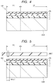
- Fig. 3 is a process flow view illustrating part of a process flow of the semiconductor device
- Figs. 4 to 14 are essential-part sectional views each illustrating a manufacturing step of a semiconductor device.
- Fig. 15 is a plan view of the semiconductor wafer, illustrating an exposure region.
- a semiconductor substrate SUB including, for example, silicon is first provided (Step S1 in Fig. 3 .)
- the semiconductor substrate SUB is the semiconductor wafer SW whose planar shape is circular (approximately circular).
- Fig. 4 illustrates part of each of a peripheral portion PC and a central portion CP of the semiconductor wafer SW.
- the peripheral portion PC includes at least the later-described first wafer edge exposure region WEE1 and second wafer edge exposure region WEE2.
- the central portion CP means a central portion (inner portion) of the semiconductor wafer SW, the central portion being located inside the peripheral portion PC.
- the sectional shape of the outer periphery of the semiconductor wafer SW is briefly illustrated as a rectangular shape, but actually the corners on the main surface side and the rear surface side of the semiconductor wafer SW are chamfered in the thickness direction, as illustrated in Fig. 2 .
- a film to be processed (layer to be processed) 2 is formed over the semiconductor substrate SUB via an insulating film 1 including, for example, a silicon oxide film (Step S2 in Fig. 3 .)
- the film to be processed 2 includes, for example, a silicon nitride film.
- an antireflection film is formed over the film to be processed 2.
- a BARL (Bottom Antireflective Layer) using an inorganic film or a BARC (Bottom Antireflective Coating) using an organic film is used as the antireflection film.
- the BARC is formed by using coating and thermal curing.
- a tri-layer resist process may be adopted, in which a Bottom layer 3 and a middle layer 4 are used as the antireflection film.
- the middle layer 4 functions as a mask for processing the bottom layer 3 while the bottom layer 3 as a mask for processing the film to be processed 2 in terms of processing.
- the tri-layer resist process is adopted for the antireflection film.
- the bottom layer 3 was formed as follows: for example, a chemical solution HM8005 (made by JSR Corp.) was coated by a spin coating method so as to have a thickness of 200 nm; and then a polymer was crosslinked by a heat treatment.
- the middle layer (middle layer film) 4 containing carbon (C) and silicon (Si) as main components, was formed over the bottom layer 3.
- the middle layer 4 was formed by using SHB-A759 (made by Shin-Etsu Chemical Co., Ltd.) as a base material (base resin). After the material was coated by a spin coating method so as to have a thickness of 80 nm, the base polymer was crosslinked by a heat treatment at 180°C for 90 seconds, thereby allowing the middle layer 4 to be formed.
- the resist layer (photosensitive resist layer, top-coatless resist layer, resist film) PR is formed by spin coating a top-coatless resist (Step S3 in Fig. 3 .) The coating was followed by thermal curing.
- the resist layer PR is formed by using a chemically amplified positive resist.
- the material of the resist layer PR is made by dissolving these materials (the aforementioned base polymer, PAG, quencher, and water-repellent additive) in PGMEA (propylene glycol monomethyl ether a
- the resist layer PR was coated by a spin coating method so as to have a thickness of 100 nm followed by a heat treatment at 100°C for 60 seconds.
- the water-repellent additive added to the resist layer PR was surface-segregated during the spin coating, and as a result, the resist layer PR exhibited a high water-repellent property in which the receding contact angle of the resist layer PR was 75.0.
- first wafer edge exposure is performed in a region (outer peripheral region) near to the outer periphery WF of the semiconductor wafer SW, as illustrated in Fig. 5 (Step S4 in Fig. 3 .)
- a region having a first width (e.g., 1 mm) from the outer periphery WF of the semiconductor wafer SW is selectively irradiated with exposure light by using a photomask MK2, as illustrated in Figs. 5 and 15 .
- the region irradiated with exposure light is the first wafer edge exposure region WEE1.
- the first wafer edge exposure region WEE1 is a region between the outer periphery WF and a first wafer edge exposure region inner periphery W1.
- DUV Deep Ultraviolet
- the resist layer PR when the resist layer PR was irradiated, for example, at a light exposure of 100 mJ/cm 2 , with exposure light having a wavelength of 200 nm emitted from a mercury xenon lamp, an acid was generated from a photo-acid generating agent in the chemically amplified positive resist, and the generated acid caused the deprotection reaction of the base resin of the resist to partially progress, so that a polar group appeared in the base resin.
- the receding contact angle of the surface of the resist layer PR in the first wafer edge exposure region WEE1 was lowered to 72.0. That is, the water-repellent property of the resist layer PR in the first wafer edge exposure region WEE1 was lowered by the first wafer edge exposure.
- liquid immersion exposure is performed, as illustrated in Figs. 6 and 15 (Step S5 in Fig. 3 .)
- Liquid immersion exposure is performed on the resist layer PR formed over the main surface of the semiconductor wafer SW, as described with reference to Figs. 1 and 2 .
- the pattern formed in the photomask (reticle) MK1 is imaged over the resist layer PR by reduced projection exposure, and the light exposure of exposure light having a wavelength of 193 nm was set to 20 mJ/cm 2 .
- the liquid immersion exposure is scanning exposure in which chip regions CH are sequentially formed over the main surface of the semiconductor wafer SW by scanning the semiconductor wafer SW with respect to the lens LS.
- the chip regions CH are arranged over the main surface of the semiconductor wafer SW and in a matrix pattern in the vertical and horizontal directions, and they are also formed across the entire circumference of the outer periphery WF of the semiconductor wafer SW. That is, the outer periphery WF of the semiconductor wafer SW is located inside the chip regions CH arranged in a matrix pattern (in other words, inside a liquid immersion exposure region IL.) Because the liquid immersion exposure is performed on the outer periphery WF of the semiconductor wafer SW, the aforementioned problems regarding the bubble VD are caused.
- the reason why the chip regions CH are formed also across the outer periphery WF of the semiconductor wafer SW is that processing accuracy and yield are improved by matching the environments of processing, such as exposure, etching, or the like, for both the chip regions CH located in the central portion CP of the semiconductor wafer SW and those located in the peripheral portion PC. Also, it is because the number of the chip regions CH over the semiconductor wafer SW is increased.
- Fig. 6 illustrates an example in which only a partial portion of the central portion CP of the semiconductor wafer SW is irradiated with the exposure light in the liquid immersion exposure.
- second wafer edge exposure is performed in the outer periphery of the semiconductor wafer SW, as illustrated in Fig. 7 (Step S6 in Fig. 3 .)
- a region having a second width (e.g., 1.5 mm) from the outer periphery WF of the semiconductor wafer SW is selectively irradiated with exposure light by using a photomask MK3, as illustrated in Figs. 7 and 15 .
- the region irradiated with exposure light is the second wafer edge exposure region WEE2.
- the second wafer edge exposure region WEE2 is a region between the outer periphery WF and a second wafer edge exposure region inner periphery W2.
- it is preferable to employ dry exposure using DUV light having a wavelength longer than that of the light used in the liquid immersion exposure in order to reduce processing time and cost.
- the second wafer edge exposure is performed in order to remove, in the later-described developing step, the resist layer PR in an area near to the outer periphery WF of the semiconductor wafer SW.
- the thickness of the resist layer PR in the area near to the outer periphery WF of the semiconductor wafer SW is more likely to vary in comparison with the central portion CP. This is because the circumference of the semiconductor wafer SW is chamfered in the thickness direction, or because the resist layer PR is coated by a spin coating method, or the like.
- the variation in the film thickness causes a pattern defect of the film to be processed 2 in the area near to the outer periphery WF of the semiconductor wafer SW.
- the second wafer edge exposure is performed in order to remove the resist layer PR in a region where a variation in the thickness of the resist layer PR is to be caused.
- the second wafer edge exposure region inner periphery W2 is located more inside the main surface of the semiconductor wafer SW (located nearer to the center) than the first wafer edge exposure region inner periphery W1. That is, an influence of the exposure light in the first wafer edge exposure, which may be affected on the chip regions CH formed inside the second wafer edge exposure region inner periphery W2 (formed near to the center), can be prevented (reduced) by separating the second wafer edge exposure region inner periphery W2 from the first wafer edge exposure region inner periphery W1.
- the second wafer edge exposure region inner periphery W2 may be set at a distance of 2 mm from the outer periphery WF.
- the resist layer PR is irradiated, for example, at a light exposure of 60 mJ/cm 2 , with exposure light emitted from a mercury xenon lamp,
- PEB Post Exposure Bake
- an acid is generated from the acid generating agent contained in the resist layer PR in the region irradiated with the exposure light (ultraviolet light). Further, a deprotection reaction is caused to progress in the resist layer PR in the irradiated region by performing the PEB.
- the acid generated in the irradiated region acts on an alkali dissolution inhibiting group of the base resin, the alkali dissolution inhibiting group being acid-dissociable, so that the base resin is decomposed, which changes the resist layer PR so as to have a molecular structure dissoluble in an alkali developer.
- a TMAH liquid alkaline tetramethylammonium hydroxide liquid
- a developer an alkaline tetramethylammonium hydroxide liquid (hereinafter, referred to as a TMAH liquid), or the like, is used as a developer, and the development is performed for 30 seconds.
- the resist layer PR in the region irradiated with exposure light is dissolved by the development, so that a resist pattern PRa is completed and the middle layer 4 is exposed from an opening that is a dissolved area of the resist layer PR.
- the resist layer PR in each of the region irradiated with ArF excimer laser exposure light and the second wafer edge exposure region WEE2 is removed.
- the middle layer 4 and the bottom layer 3 are etched, as illustrated in Fig. 9 (Step S8 in Fig. 3 .)
- the middle layer 4 was dry etched by using mixed gas of CHF 3 , CF 4 , and O 2 with the use of the resist pattern PRa as a mask, thereby allowing the pattern of the resist pattern PRa to be transferred to the middle layer 4.
- the bottom layer 3 is dry etched by using mixed gas of O 2 , N 2 , and HBr with the use of the pattern formed by the resist pattern PRa and the middle layer 4 as a mask, thereby allowing a bottom layer pattern 3a, to which the pattern of the resist pattern PRa has been transferred, to be completed.
- the resist pattern PRa and the middle layer 4 are removed and disappear.
- the film to be processed 2 is etched by using the bottom layer pattern 3a as a mask and a trench GV is formed, as illustrated in Fig. 10 (Step S9 in Fig. 3 .)
- the silicon nitride film that is the film to be processed 2, the insulating film 1, and the semiconductor substrate (silicon substrate) SUB are sequentially dry etched by using mixed gas of Cl, HBr, SF 6 , and O 2 . Because the resist pattern PRa of the resist layer PR is transferred to the film to be processed 2 and the trench GV is formed in the semiconductor substrate SUB by using the film to be processed 2 as a mask, the trench GV is formed at a position corresponding to the opening of the resist pattern PRa.
- an element isolation insulating film 5 including, for example, a silicon oxide film is deposited over the semiconductor substrate SUB by a CVD (Chemical Vapor Deposition) method, so that the trench GV is filled with the element isolation insulating film 5, as illustrated in Fig. 11 .
- CVD Chemical Vapor Deposition
- the element isolation insulating film 5 is selectively left only in the trench GV by performing CMP (Chemical Mechanical Polishing) processing on the element isolation insulating film 5, thereby allowing an element isolation region STI to be formed, as illustrated in Fig. 12
- a gate insulating film GI and a gate electrode GE are formed over the main surface of the semiconductor substrate SUB, as illustrated in Fig. 13 .
- an active region surrounded, in plan view, by the element isolation region STI is formed over the main surface of the semiconductor substrate SUB.
- an insulating film to become the gate insulating film GI and a conductor film to become the gate electrode GE are formed over the main surface of the semiconductor substrate SUB.
- the gate electrode GE and the gate insulating film GI are formed by etching the conductor film and the insulating film.
- the gate electrode GE can be formed by performing Step S3 to Step S9 in Fig. 3 with the use of the conductor film as the aforementioned film to be processed.
- the gate insulating film GI can be formed by a silicon oxide film, a silicon oxynitride film, or the like.
- the gate electrode GE can be formed by a polycrystalline silicon film, a metal film, or the like.
- the conductor film may be caused to correspond to the semiconductor substrate SUB.
- the etching step of forming the trench GV in the semiconductor substrate SUB corresponds to the step of etching the conductor film in order to form the gate electrode GE.
- a low-concentration semiconductor region NM is sequentially formed, as illustrated in Fig. 14 .
- the low-concentration semiconductor region NM is first formed over the surface of the semiconductor substrate SUB at both the ends of the gate electrode GE.
- the low-concentration semiconductor region NM is, for example, an n-type semiconductor region, and is formed by ion-implanting impurities, such as phosphorus (P), arsenic (As), or the like, in a self-aligned manner to the gate electrode GE.
- the sidewall insulating film SP can be selectively formed over the sidewall of the gate electrode GE by depositing an insulating film so as to cover the upper surface and the side surface of the gate electrode GE and then by performing anisotropic dry etching on the insulating film.
- the sidewall insulating film SP may include a silicon oxide film, a silicon nitride film, or a laminated structure of the two.
- the high-concentration semiconductor region NH is formed over the surface of the semiconductor substrate SUB at both the ends of the gate electrode GE.
- the high-concentration semiconductor region NH is, for example, an n-type semiconductor region, and is formed by ion-implanting impurities, such as phosphorus (P), arsenic (As), or the like, in a self-aligned manner with respect to the gate electrode GE and the sidewall insulating film SP.
- the MISFET is formed by the gate electrode GE, the gate insulating film GI, the low-concentration semiconductor region NM, and the high-concentration semiconductor region NH.
- the source and drain of the MISFET are formed by the low-concentration semiconductor region NM and the high-concentration semiconductor region NH.
- the water-repellent property of the resist layer PR to be used in liquid immersion exposure is lowered by performing first wafer edge exposure on the resist layer PR before the liquid immersion exposure, thereby allowing the engulfment of the bubble VD to be prevented and a pattern defect of the resist pattern PRa to be prevented in the liquid immersion exposure.
- a pattern defect of each of a silicon nitride film, which is the film to be processed 2 to which the pattern of the resist pattern PRa has been transferred, and the element isolation region STI can be prevented, thereby allowing a semiconductor device with high reliability to be provided. Furthermore, the manufacturing yield of a semiconductor device can be improved.
- the engulfment of the bubble VD is noticeable, the light exposure in the first wafer edge exposure is increased. Thereby, the hydrophilic property of the first wafer edge exposure region WEE1 can be increased to a higher level, so that the engulfment of the bubble VD can be suppressed. If water leak is caused in the gap GP by performing the first wafer edge exposure, the light exposure in the first wafer edge exposure is reduced. Thereby, the excessive hydrophilic property of the resist surface, which may be caused by performing the first wafer edge exposure, can be improved.
- the light exposure in the first wafer edge exposure can be easily changed by performing the first wafer edge exposure and the second wafer edge exposure in different steps, thereby allowing the engulfment of the bubble VD, which may be caused during liquid immersion exposure, to be prevented.
- the exposure light, with which the first wafer edge exposure region WEE1 is irradiated never adversely affects the chip region CH formed inside the second wafer edge exposure region WEE2 (formed inside (near to the center of) the second wafer edge exposure region inner periphery W2), even when the light exposure in the first wafer edge exposure is changed. Accordingly, the light exposure in the first wafer edge exposure can be increased sufficiently, and hence the water-repellent property of the resist layer PR can be lowered sufficiently.
- an exposure apparatus using, for example, DUV light can be adopted for the first wafer edge exposure, and hence both the processing time of the first wafer edge exposure and manufacturing cost can be reduced. Because an exposure apparatus using DUV light can also be adopted for the second wafer edge exposure, similar effects can be obtained.
- the surface of the semiconductor wafer SW (resist layer PR) is subjected to a washing treatment by deionized water immediately after the first wafer edge exposure of Step S4 in Fig. 3 .
- the deprotection reaction of the base resin that forms the resist layer PR partially progresses immediately after the first wafer edge exposure, so that a polar group appears. Because the polar group has a high affinity with water, the orientation thereof is changed in a direction toward the surface of the resist layer PR when water is supplied to the surface thereof, thereby allowing the hydrophilic property of the resist layer PR to be improved.
- the aforementioned washing treatment is effective particularly when the water-repellent property of the resist layer PR cannot be sufficiently lowered in the first wafer edge exposure, and the like.
- a heat treatment is performed on the semiconductor wafer SW immediately after the first wafer edge exposure of Step S4 in Fig. 3 . It is preferable that the heat treatment is performed under the conditions at 70°C for approximately 10 seconds, the temperature and time being set to be lower and shorter than the conditions of the PEB.
- the deprotection reaction of the resist layer PR in the first wafer edge exposure region WEE1 can be caused to progress to a further level, so that the water-repellent property is greatly lowered.
- the heat treatment is effective particularly when the water-repellent property of the resist layer PR cannot be sufficiently lowered in the first wafer edge exposure, and the like.
- the second wafer edge exposure is performed before the liquid immersion exposure in the process flow in Fig. 3 .
- Either the first wafer edge exposure or the second wafer edge exposure may be performed first as long as they are performed before the liquid immersion exposure, but it is important to perform both of them.
- Exposure conditions are the same as those in the aforementioned embodiment, and the first wafer edge exposure and the second wafer edge exposure are performed on different regions and under different conditions, respectively. That is, it is important to make the width of the second wafer edge exposure region WEE2 larger than that of the first wafer edge exposure region WEE1 for controlling the water-repellent property.
- the chip region CH formed inside the second wafer edge exposure region WEE2 (formed inside (near to the center of) the second wafer edge exposure region inner periphery W2) cannot be adversely affected by the exposure light in the first wafer edge exposure.
- the first wafer edge exposure can be omitted; however, the chip region inside the second wafer edge exposure region inner periphery W2 in Fig. 15 is affected, and hence it is preferable to perform the first wafer edge exposure and the second wafer edge exposure together.
- the first wafer edge exposure and the second wafer edge exposure can be performed in a single exposure apparatus unit, and hence the processing time of the exposure steps can be reduced.
- it is common that the first wafer edge exposure, the liquid immersion exposure, and the second wafer edge exposure are performed in exposure apparatus units different from each other.
- the first wafer edge exposure and the second wafer edge exposure can be performed in a single exposure apparatus unit, and hence both the time for transfers among units and throughput can be reduced.
- a semiconductor device according to the present embodiment can be thus manufactured.
- the present invention has been described by using an example in which, for example, the resist layer PR is formed over the film to be processed 2 via the bottom layer 3 and the middle layer 4, but the middle layer 4, the bottom layer 3, or both of the two may be omitted.
Landscapes
- Physics & Mathematics (AREA)
- General Physics & Mathematics (AREA)
- Engineering & Computer Science (AREA)
- Power Engineering (AREA)
- Microelectronics & Electronic Packaging (AREA)
- Manufacturing & Machinery (AREA)
- Condensed Matter Physics & Semiconductors (AREA)
- Computer Hardware Design (AREA)
- Chemical & Material Sciences (AREA)
- General Chemical & Material Sciences (AREA)
- Chemical Kinetics & Catalysis (AREA)
- Spectroscopy & Molecular Physics (AREA)
- Architecture (AREA)
- Structural Engineering (AREA)
- Inorganic Chemistry (AREA)
- Ceramic Engineering (AREA)
- Exposure Of Semiconductors, Excluding Electron Or Ion Beam Exposure (AREA)
- Exposure And Positioning Against Photoresist Photosensitive Materials (AREA)
Applications Claiming Priority (1)
| Application Number | Priority Date | Filing Date | Title |
|---|---|---|---|
| JP2015099065A JP6456238B2 (ja) | 2015-05-14 | 2015-05-14 | 半導体装置の製造方法 |
Publications (1)
| Publication Number | Publication Date |
|---|---|
| EP3093712A1 true EP3093712A1 (en) | 2016-11-16 |
Family
ID=55806193
Family Applications (1)
| Application Number | Title | Priority Date | Filing Date |
|---|---|---|---|
| EP16166157.4A Withdrawn EP3093712A1 (en) | 2015-05-14 | 2016-04-20 | Photolithographic process for manufacturing a semiconductor device |
Country Status (6)
| Country | Link |
|---|---|
| US (3) | US9627203B2 (ja) |
| EP (1) | EP3093712A1 (ja) |
| JP (1) | JP6456238B2 (ja) |
| KR (1) | KR20160134515A (ja) |
| CN (1) | CN106158598B (ja) |
| TW (1) | TWI699821B (ja) |
Families Citing this family (6)
| Publication number | Priority date | Publication date | Assignee | Title |
|---|---|---|---|---|
| KR102614850B1 (ko) * | 2016-10-05 | 2023-12-18 | 삼성전자주식회사 | 반도체 소자 제조방법 |
| WO2018216566A1 (ja) * | 2017-05-25 | 2018-11-29 | 東京エレクトロン株式会社 | 基板処理方法、記憶媒体及び基板処理システム |
| JP6938260B2 (ja) * | 2017-07-20 | 2021-09-22 | 株式会社ディスコ | ウエーハの研削方法 |
| CN108319057A (zh) * | 2018-03-29 | 2018-07-24 | 武汉华星光电技术有限公司 | 基板边缘处理方法、掩膜版 |
| US11626285B2 (en) * | 2019-09-10 | 2023-04-11 | Taiwan Semiconductor Manufacturing Co., Ltd. | Method of manufacturing a semiconductor device |
| CN113506746B (zh) * | 2021-06-28 | 2024-03-19 | 华虹半导体(无锡)有限公司 | 解决超级结工艺打标区域高台阶差的方法 |
Citations (7)
| Publication number | Priority date | Publication date | Assignee | Title |
|---|---|---|---|---|
| JP2006108564A (ja) | 2004-10-08 | 2006-04-20 | Renesas Technology Corp | 電子デバイスの製造方法および露光システム |
| JP2006528835A (ja) | 2003-07-24 | 2006-12-21 | カール・ツアイス・エスエムテイ・アーゲー | マイクロリソグラフィ投影露光装置および浸漬液体を浸漬空間へ導入する方法 |
| JP2008235542A (ja) | 2007-03-20 | 2008-10-02 | Dainippon Printing Co Ltd | 液浸リソグラフィ用ウェハおよびその製造方法 |
| JP2009088552A (ja) | 2004-02-09 | 2009-04-23 | Asml Netherlands Bv | リソグラフィ装置およびリソグラフィ装置を清浄する方法 |
| JP2009117873A (ja) | 2004-12-07 | 2009-05-28 | Asml Netherlands Bv | 浸漬露光前の基板のプレウェッティング |
| EP2228684A2 (en) * | 2009-03-13 | 2010-09-15 | Tokyo Electron Limited | Coating and developing apparatus, coating and developing method, and storage medium |
| US20120141944A1 (en) * | 2008-06-04 | 2012-06-07 | Kabushiki Kaisha Toshiba | Method for manufacturing semiconductor device |
Family Cites Families (29)
| Publication number | Priority date | Publication date | Assignee | Title |
|---|---|---|---|---|
| JPH11162803A (ja) * | 1997-12-01 | 1999-06-18 | Seiko Epson Corp | ポジレジストの処理方法 |
| US20040067654A1 (en) * | 2002-10-07 | 2004-04-08 | Promos Technologies, Inc. | Method of reducing wafer etching defect |
| JP2004297032A (ja) * | 2003-02-03 | 2004-10-21 | Toshiba Corp | 露光方法及びこれを用いた半導体装置製造方法 |
| KR20050002359A (ko) * | 2003-06-30 | 2005-01-07 | 주식회사 하이닉스반도체 | 반도체 소자의 패턴 형성방법 |
| KR100724478B1 (ko) * | 2003-06-30 | 2007-06-04 | 엘지.필립스 엘시디 주식회사 | 액정표시소자 제조방법 |
| JP4220423B2 (ja) * | 2004-03-24 | 2009-02-04 | 株式会社東芝 | レジストパターン形成方法 |
| KR20050113457A (ko) * | 2004-05-29 | 2005-12-02 | 주식회사 하이닉스반도체 | 낸드 플래시 메모리 소자의 제조 방법 |
| US8294873B2 (en) * | 2004-11-11 | 2012-10-23 | Nikon Corporation | Exposure method, device manufacturing method, and substrate |
| JP4634822B2 (ja) * | 2005-02-24 | 2011-02-16 | 株式会社東芝 | レジストパターン形成方法および半導体装置の製造方法 |
| JP4654120B2 (ja) * | 2005-12-08 | 2011-03-16 | 東京エレクトロン株式会社 | 塗布、現像装置及び塗布、現像方法並びにコンピュータプログラム |
| JP4368365B2 (ja) * | 2006-08-02 | 2009-11-18 | Tdk株式会社 | 液浸露光用基板およびその製造方法、ならびに液浸露光方法 |
| JP4357514B2 (ja) * | 2006-09-29 | 2009-11-04 | 株式会社東芝 | 液浸露光方法 |
| JP4859229B2 (ja) * | 2006-12-08 | 2012-01-25 | 東京エレクトロン株式会社 | 熱処理装置 |
| US8617794B2 (en) * | 2007-06-12 | 2013-12-31 | Fujifilm Corporation | Method of forming patterns |
| JP5035562B2 (ja) * | 2007-08-22 | 2012-09-26 | 信越化学工業株式会社 | パターン形成方法 |
| US7824846B2 (en) * | 2007-09-19 | 2010-11-02 | International Business Machines Corporation | Tapered edge bead removal process for immersion lithography |
| US20090107519A1 (en) * | 2007-10-30 | 2009-04-30 | Sokudo Co., Ltd. | Method and system for chemically enhanced laser trimming of substrate edges |
| US8197996B2 (en) * | 2008-09-19 | 2012-06-12 | Tokyo Electron Limited | Dual tone development processes |
| JP5181306B2 (ja) * | 2009-01-30 | 2013-04-10 | セメス株式会社 | 基板処理システム、露光前後処理ユニット及び基板処理方法 |
| JP2010182732A (ja) * | 2009-02-03 | 2010-08-19 | Toshiba Corp | 半導体装置の製造方法 |
| US8551566B2 (en) * | 2009-02-19 | 2013-10-08 | Massachusetts Institute Of Technology | Directed material assembly |
| CN101571674A (zh) * | 2009-06-09 | 2009-11-04 | 上海集成电路研发中心有限公司 | 一种双重曝光方法 |
| US7845868B1 (en) * | 2009-09-09 | 2010-12-07 | Nanya Technology Corporation | Apparatus for semiconductor manufacturing process |
| IL213195A0 (en) * | 2010-05-31 | 2011-07-31 | Rohm & Haas Elect Mat | Photoresist compositions and emthods of forming photolithographic patterns |
| US8232198B2 (en) * | 2010-08-05 | 2012-07-31 | International Business Machines Corporation | Self-aligned permanent on-chip interconnect structure formed by pitch splitting |
| US20120045721A1 (en) * | 2010-08-18 | 2012-02-23 | Tokyo Electron Limited | Method for forming a self-aligned double pattern |
| JP5816488B2 (ja) * | 2011-08-26 | 2015-11-18 | ルネサスエレクトロニクス株式会社 | 半導体装置の製造方法 |
| US9372406B2 (en) * | 2012-04-13 | 2016-06-21 | Taiwan Semiconductor Manufacturing Company, Ltd. | Film portion at wafer edge |
| US9140987B2 (en) * | 2014-02-21 | 2015-09-22 | Taiwan Semiconductor Manufacturing Company, Ltd. | Method for lithography patterning |
-
2015
- 2015-05-14 JP JP2015099065A patent/JP6456238B2/ja active Active
-
2016
- 2016-04-20 EP EP16166157.4A patent/EP3093712A1/en not_active Withdrawn
- 2016-04-25 US US15/137,964 patent/US9627203B2/en active Active
- 2016-04-25 TW TW105112740A patent/TWI699821B/zh active
- 2016-05-11 KR KR1020160057451A patent/KR20160134515A/ko not_active Application Discontinuation
- 2016-05-12 CN CN201610312858.0A patent/CN106158598B/zh active Active
-
2017
- 2017-03-07 US US15/451,525 patent/US9847226B2/en active Active
- 2017-11-13 US US15/811,282 patent/US20180068845A1/en not_active Abandoned
Patent Citations (7)
| Publication number | Priority date | Publication date | Assignee | Title |
|---|---|---|---|---|
| JP2006528835A (ja) | 2003-07-24 | 2006-12-21 | カール・ツアイス・エスエムテイ・アーゲー | マイクロリソグラフィ投影露光装置および浸漬液体を浸漬空間へ導入する方法 |
| JP2009088552A (ja) | 2004-02-09 | 2009-04-23 | Asml Netherlands Bv | リソグラフィ装置およびリソグラフィ装置を清浄する方法 |
| JP2006108564A (ja) | 2004-10-08 | 2006-04-20 | Renesas Technology Corp | 電子デバイスの製造方法および露光システム |
| JP2009117873A (ja) | 2004-12-07 | 2009-05-28 | Asml Netherlands Bv | 浸漬露光前の基板のプレウェッティング |
| JP2008235542A (ja) | 2007-03-20 | 2008-10-02 | Dainippon Printing Co Ltd | 液浸リソグラフィ用ウェハおよびその製造方法 |
| US20120141944A1 (en) * | 2008-06-04 | 2012-06-07 | Kabushiki Kaisha Toshiba | Method for manufacturing semiconductor device |
| EP2228684A2 (en) * | 2009-03-13 | 2010-09-15 | Tokyo Electron Limited | Coating and developing apparatus, coating and developing method, and storage medium |
Also Published As
| Publication number | Publication date |
|---|---|
| TW201709275A (zh) | 2017-03-01 |
| JP2016218099A (ja) | 2016-12-22 |
| CN106158598B (zh) | 2021-11-02 |
| JP6456238B2 (ja) | 2019-01-23 |
| US20160336173A1 (en) | 2016-11-17 |
| US9627203B2 (en) | 2017-04-18 |
| US9847226B2 (en) | 2017-12-19 |
| KR20160134515A (ko) | 2016-11-23 |
| TWI699821B (zh) | 2020-07-21 |
| CN106158598A (zh) | 2016-11-23 |
| US20180068845A1 (en) | 2018-03-08 |
| US20170178897A1 (en) | 2017-06-22 |
Similar Documents
| Publication | Publication Date | Title |
|---|---|---|
| US9847226B2 (en) | Manufacturing method of semiconductor device | |
| CN108227392B (zh) | 微影图案化的方法 | |
| US8029969B2 (en) | Material and method for photolithography | |
| CN109427553B (zh) | 保护晶圆免受斜面污染的半导体方法 | |
| US20120034558A1 (en) | Photolithography material for immersion lithography processes | |
| TWI584083B (zh) | 用於微影製程之圖案化的方法 | |
| US20090246958A1 (en) | Method for removing residues from a patterned substrate | |
| US11387104B2 (en) | Grafting design for pattern post-treatment in semiconductor manufacturing | |
| US7662542B2 (en) | Pattern forming method and semiconductor device manufacturing method | |
| US10520821B2 (en) | Lithography process with enhanced etch selectivity | |
| TWI401542B (zh) | 移除上塗層而減低浸潤式微影之缺陷 | |
| US7755740B2 (en) | Exposure apparatus | |
| CN116053116B (zh) | 一种半导体器件图形化的方法 | |
| US20080156346A1 (en) | Method and apparatus for cleaning a substrate | |
| US20220057715A1 (en) | Substrate treating composition and method for fabricating a semiconductor device using the same | |
| US8084192B2 (en) | Method for forming resist pattern | |
| US20230062148A1 (en) | Method and system for manufacturing a semiconductor device | |
| US9625822B2 (en) | Mechanisms for performing a photolithography process with a surface modifying treatment on an exposed photoresist layer | |
| US8026183B2 (en) | Method of forming a resist pattern | |
| KR100960483B1 (ko) | 반도체소자 제조방법 | |
| JP2006196575A (ja) | 液浸型露光方法によるレジストパターン形成方法 |
Legal Events
| Date | Code | Title | Description |
|---|---|---|---|
| PUAI | Public reference made under article 153(3) epc to a published international application that has entered the european phase |
Free format text: ORIGINAL CODE: 0009012 |
|
| AK | Designated contracting states |
Kind code of ref document: A1 Designated state(s): AL AT BE BG CH CY CZ DE DK EE ES FI FR GB GR HR HU IE IS IT LI LT LU LV MC MK MT NL NO PL PT RO RS SE SI SK SM TR |
|
| AX | Request for extension of the european patent |
Extension state: BA ME |
|
| 17P | Request for examination filed |
Effective date: 20170512 |
|
| RBV | Designated contracting states (corrected) |
Designated state(s): AL AT BE BG CH CY CZ DE DK EE ES FI FR GB GR HR HU IE IS IT LI LT LU LV MC MK MT NL NO PL PT RO RS SE SI SK SM TR |
|
| STAA | Information on the status of an ep patent application or granted ep patent |
Free format text: STATUS: THE APPLICATION IS DEEMED TO BE WITHDRAWN |
|
| 18D | Application deemed to be withdrawn |
Effective date: 20191101 |