EP2942803A1 - Kristalline mehrschichtige Struktur und Halbleiterbauelement - Google Patents
Kristalline mehrschichtige Struktur und Halbleiterbauelement Download PDFInfo
- Publication number
- EP2942803A1 EP2942803A1 EP14199100.0A EP14199100A EP2942803A1 EP 2942803 A1 EP2942803 A1 EP 2942803A1 EP 14199100 A EP14199100 A EP 14199100A EP 2942803 A1 EP2942803 A1 EP 2942803A1
- Authority
- EP
- European Patent Office
- Prior art keywords
- thin film
- oxide semiconductor
- crystalline
- multilayer structure
- type semiconductor
- Prior art date
- Legal status (The legal status is an assumption and is not a legal conclusion. Google has not performed a legal analysis and makes no representation as to the accuracy of the status listed.)
- Granted
Links
- 239000004065 semiconductor Substances 0.000 title claims abstract description 268
- 239000010409 thin film Substances 0.000 claims abstract description 122
- 239000000758 substrate Substances 0.000 claims abstract description 62
- 229910052732 germanium Inorganic materials 0.000 claims abstract description 33
- GNPVGFCGXDBREM-UHFFFAOYSA-N germanium atom Chemical compound [Ge] GNPVGFCGXDBREM-UHFFFAOYSA-N 0.000 claims abstract description 33
- 239000010936 titanium Substances 0.000 claims abstract description 32
- 229910052719 titanium Inorganic materials 0.000 claims abstract description 30
- 239000010955 niobium Substances 0.000 claims abstract description 27
- 229910052720 vanadium Inorganic materials 0.000 claims abstract description 27
- 229910052758 niobium Inorganic materials 0.000 claims abstract description 26
- 229910052726 zirconium Inorganic materials 0.000 claims abstract description 26
- RTAQQCXQSZGOHL-UHFFFAOYSA-N Titanium Chemical compound [Ti] RTAQQCXQSZGOHL-UHFFFAOYSA-N 0.000 claims abstract description 21
- 229910052710 silicon Inorganic materials 0.000 claims abstract description 21
- 239000010703 silicon Substances 0.000 claims abstract description 21
- XUIMIQQOPSSXEZ-UHFFFAOYSA-N Silicon Chemical compound [Si] XUIMIQQOPSSXEZ-UHFFFAOYSA-N 0.000 claims abstract description 20
- GUCVJGMIXFAOAE-UHFFFAOYSA-N niobium atom Chemical compound [Nb] GUCVJGMIXFAOAE-UHFFFAOYSA-N 0.000 claims abstract description 20
- LEONUFNNVUYDNQ-UHFFFAOYSA-N vanadium atom Chemical compound [V] LEONUFNNVUYDNQ-UHFFFAOYSA-N 0.000 claims abstract description 20
- QCWXUUIWCKQGHC-UHFFFAOYSA-N Zirconium Chemical compound [Zr] QCWXUUIWCKQGHC-UHFFFAOYSA-N 0.000 claims abstract description 19
- GYHNNYVSQQEPJS-UHFFFAOYSA-N Gallium Chemical compound [Ga] GYHNNYVSQQEPJS-UHFFFAOYSA-N 0.000 claims abstract description 18
- 229910052733 gallium Inorganic materials 0.000 claims abstract description 18
- 229910052738 indium Inorganic materials 0.000 claims abstract description 18
- APFVFJFRJDLVQX-UHFFFAOYSA-N indium atom Chemical compound [In] APFVFJFRJDLVQX-UHFFFAOYSA-N 0.000 claims abstract description 12
- 229910052751 metal Inorganic materials 0.000 claims description 21
- 239000002184 metal Substances 0.000 claims description 19
- 230000005669 field effect Effects 0.000 claims description 17
- 229910052799 carbon Inorganic materials 0.000 claims description 15
- 229910044991 metal oxide Inorganic materials 0.000 claims description 14
- 150000004706 metal oxides Chemical class 0.000 claims description 14
- 230000004888 barrier function Effects 0.000 claims description 10
- OKTJSMMVPCPJKN-UHFFFAOYSA-N Carbon Chemical compound [C] OKTJSMMVPCPJKN-UHFFFAOYSA-N 0.000 claims description 7
- 230000006698 induction Effects 0.000 claims description 4
- 230000003068 static effect Effects 0.000 claims description 4
- 239000010410 layer Substances 0.000 description 167
- 239000010408 film Substances 0.000 description 44
- 239000002994 raw material Substances 0.000 description 41
- 239000000243 solution Substances 0.000 description 39
- 239000002019 doping agent Substances 0.000 description 31
- 239000000523 sample Substances 0.000 description 26
- 239000007864 aqueous solution Substances 0.000 description 25
- 238000000034 method Methods 0.000 description 24
- 239000012212 insulator Substances 0.000 description 22
- 239000000463 material Substances 0.000 description 22
- 239000013078 crystal Substances 0.000 description 21
- 239000012159 carrier gas Substances 0.000 description 20
- 238000010586 diagram Methods 0.000 description 19
- 239000011135 tin Substances 0.000 description 19
- IJGRMHOSHXDMSA-UHFFFAOYSA-N Atomic nitrogen Chemical compound N#N IJGRMHOSHXDMSA-UHFFFAOYSA-N 0.000 description 18
- QZQVBEXLDFYHSR-UHFFFAOYSA-N gallium(III) oxide Inorganic materials O=[Ga]O[Ga]=O QZQVBEXLDFYHSR-UHFFFAOYSA-N 0.000 description 18
- 150000001875 compounds Chemical class 0.000 description 17
- XLOMVQKBTHCTTD-UHFFFAOYSA-N Zinc monoxide Chemical compound [Zn]=O XLOMVQKBTHCTTD-UHFFFAOYSA-N 0.000 description 16
- AJNVQOSZGJRYEI-UHFFFAOYSA-N digallium;oxygen(2-) Chemical compound [O-2].[O-2].[O-2].[Ga+3].[Ga+3] AJNVQOSZGJRYEI-UHFFFAOYSA-N 0.000 description 15
- 239000000203 mixture Substances 0.000 description 14
- 239000007772 electrode material Substances 0.000 description 13
- 238000004544 sputter deposition Methods 0.000 description 13
- 229910052718 tin Inorganic materials 0.000 description 13
- 230000002159 abnormal effect Effects 0.000 description 12
- 229910001195 gallium oxide Inorganic materials 0.000 description 12
- 238000000137 annealing Methods 0.000 description 11
- 239000003112 inhibitor Substances 0.000 description 11
- BMYNFMYTOJXKLE-UHFFFAOYSA-N 3-azaniumyl-2-hydroxypropanoate Chemical compound NCC(O)C(O)=O BMYNFMYTOJXKLE-UHFFFAOYSA-N 0.000 description 10
- SRVXDMYFQIODQI-UHFFFAOYSA-K gallium(iii) bromide Chemical compound Br[Ga](Br)Br SRVXDMYFQIODQI-UHFFFAOYSA-K 0.000 description 10
- 229910052594 sapphire Inorganic materials 0.000 description 10
- 229910052782 aluminium Inorganic materials 0.000 description 9
- YBMRDBCBODYGJE-UHFFFAOYSA-N germanium oxide Inorganic materials O=[Ge]=O YBMRDBCBODYGJE-UHFFFAOYSA-N 0.000 description 9
- XEEYBQQBJWHFJM-UHFFFAOYSA-N iron Substances [Fe] XEEYBQQBJWHFJM-UHFFFAOYSA-N 0.000 description 9
- 229910052757 nitrogen Inorganic materials 0.000 description 9
- PVADDRMAFCOOPC-UHFFFAOYSA-N oxogermanium Chemical compound [Ge]=O PVADDRMAFCOOPC-UHFFFAOYSA-N 0.000 description 9
- 239000010980 sapphire Substances 0.000 description 9
- 229910052593 corundum Inorganic materials 0.000 description 8
- 238000005259 measurement Methods 0.000 description 8
- XOLBLPGZBRYERU-UHFFFAOYSA-N tin dioxide Chemical compound O=[Sn]=O XOLBLPGZBRYERU-UHFFFAOYSA-N 0.000 description 8
- 238000001771 vacuum deposition Methods 0.000 description 8
- 239000011787 zinc oxide Substances 0.000 description 8
- ATJFFYVFTNAWJD-UHFFFAOYSA-N Tin Chemical compound [Sn] ATJFFYVFTNAWJD-UHFFFAOYSA-N 0.000 description 7
- 238000005229 chemical vapour deposition Methods 0.000 description 7
- 229910052804 chromium Inorganic materials 0.000 description 7
- 229910003437 indium oxide Inorganic materials 0.000 description 7
- PJXISJQVUVHSOJ-UHFFFAOYSA-N indium(iii) oxide Chemical compound [O-2].[O-2].[O-2].[In+3].[In+3] PJXISJQVUVHSOJ-UHFFFAOYSA-N 0.000 description 7
- 229910052742 iron Inorganic materials 0.000 description 7
- 238000004519 manufacturing process Methods 0.000 description 7
- 150000002739 metals Chemical class 0.000 description 7
- 239000003595 mist Substances 0.000 description 7
- 229910052759 nickel Inorganic materials 0.000 description 7
- 229910052697 platinum Inorganic materials 0.000 description 7
- 239000013074 reference sample Substances 0.000 description 7
- 229910052779 Neodymium Inorganic materials 0.000 description 6
- 229910045601 alloy Inorganic materials 0.000 description 6
- 239000000956 alloy Substances 0.000 description 6
- 239000011651 chromium Substances 0.000 description 6
- 229910052802 copper Inorganic materials 0.000 description 6
- 238000002474 experimental method Methods 0.000 description 6
- 239000010419 fine particle Substances 0.000 description 6
- 229910052737 gold Inorganic materials 0.000 description 6
- 229910052735 hafnium Inorganic materials 0.000 description 6
- 230000001771 impaired effect Effects 0.000 description 6
- AMGQUBHHOARCQH-UHFFFAOYSA-N indium;oxotin Chemical compound [In].[Sn]=O AMGQUBHHOARCQH-UHFFFAOYSA-N 0.000 description 6
- 150000002500 ions Chemical class 0.000 description 6
- 229910052741 iridium Inorganic materials 0.000 description 6
- 229910052748 manganese Inorganic materials 0.000 description 6
- 229910052750 molybdenum Inorganic materials 0.000 description 6
- 229910052763 palladium Inorganic materials 0.000 description 6
- 229920000767 polyaniline Polymers 0.000 description 6
- 229920000128 polypyrrole Polymers 0.000 description 6
- 229920000123 polythiophene Polymers 0.000 description 6
- 229910052709 silver Inorganic materials 0.000 description 6
- 229910052715 tantalum Inorganic materials 0.000 description 6
- 229910001887 tin oxide Inorganic materials 0.000 description 6
- 229910052721 tungsten Inorganic materials 0.000 description 6
- 229910052725 zinc Inorganic materials 0.000 description 6
- 239000011701 zinc Substances 0.000 description 6
- YVTHLONGBIQYBO-UHFFFAOYSA-N zinc indium(3+) oxygen(2-) Chemical compound [O--].[Zn++].[In+3] YVTHLONGBIQYBO-UHFFFAOYSA-N 0.000 description 6
- VYPSYNLAJGMNEJ-UHFFFAOYSA-N Silicium dioxide Chemical compound O=[Si]=O VYPSYNLAJGMNEJ-UHFFFAOYSA-N 0.000 description 5
- PNEYBMLMFCGWSK-UHFFFAOYSA-N aluminium oxide Inorganic materials [O-2].[O-2].[O-2].[Al+3].[Al+3] PNEYBMLMFCGWSK-UHFFFAOYSA-N 0.000 description 5
- 238000011109 contamination Methods 0.000 description 5
- 150000002259 gallium compounds Chemical class 0.000 description 5
- 238000005468 ion implantation Methods 0.000 description 5
- 229910001845 yogo sapphire Inorganic materials 0.000 description 5
- VEXZGXHMUGYJMC-UHFFFAOYSA-M Chloride anion Chemical compound [Cl-] VEXZGXHMUGYJMC-UHFFFAOYSA-M 0.000 description 4
- 230000015572 biosynthetic process Effects 0.000 description 4
- 238000005530 etching Methods 0.000 description 4
- 150000004820 halides Chemical class 0.000 description 4
- 239000012535 impurity Substances 0.000 description 4
- 230000003746 surface roughness Effects 0.000 description 4
- XLYOFNOQVPJJNP-UHFFFAOYSA-N water Substances O XLYOFNOQVPJJNP-UHFFFAOYSA-N 0.000 description 4
- UFHFLCQGNIYNRP-UHFFFAOYSA-N Hydrogen Chemical compound [H][H] UFHFLCQGNIYNRP-UHFFFAOYSA-N 0.000 description 3
- -1 aluminum compound Chemical class 0.000 description 3
- QVGXLLKOCUKJST-UHFFFAOYSA-N atomic oxygen Chemical compound [O] QVGXLLKOCUKJST-UHFFFAOYSA-N 0.000 description 3
- 239000010431 corundum Substances 0.000 description 3
- 230000002349 favourable effect Effects 0.000 description 3
- 239000007789 gas Substances 0.000 description 3
- 239000001257 hydrogen Substances 0.000 description 3
- 229910052739 hydrogen Inorganic materials 0.000 description 3
- 230000003287 optical effect Effects 0.000 description 3
- 239000001301 oxygen Substances 0.000 description 3
- 229910052760 oxygen Inorganic materials 0.000 description 3
- 239000010453 quartz Substances 0.000 description 3
- 230000002829 reductive effect Effects 0.000 description 3
- 239000000126 substance Substances 0.000 description 3
- RYSXWUYLAWPLES-MTOQALJVSA-N (Z)-4-hydroxypent-3-en-2-one titanium Chemical compound [Ti].C\C(O)=C\C(C)=O.C\C(O)=C\C(C)=O.C\C(O)=C\C(C)=O.C\C(O)=C\C(C)=O RYSXWUYLAWPLES-MTOQALJVSA-N 0.000 description 2
- CPELXLSAUQHCOX-UHFFFAOYSA-M Bromide Chemical compound [Br-] CPELXLSAUQHCOX-UHFFFAOYSA-M 0.000 description 2
- KRHYYFGTRYWZRS-UHFFFAOYSA-M Fluoride anion Chemical compound [F-] KRHYYFGTRYWZRS-UHFFFAOYSA-M 0.000 description 2
- 230000005355 Hall effect Effects 0.000 description 2
- VEXZGXHMUGYJMC-UHFFFAOYSA-N Hydrochloric acid Chemical compound Cl VEXZGXHMUGYJMC-UHFFFAOYSA-N 0.000 description 2
- CPLXHLVBOLITMK-UHFFFAOYSA-N Magnesium oxide Chemical compound [Mg]=O CPLXHLVBOLITMK-UHFFFAOYSA-N 0.000 description 2
- KJTLSVCANCCWHF-UHFFFAOYSA-N Ruthenium Chemical compound [Ru] KJTLSVCANCCWHF-UHFFFAOYSA-N 0.000 description 2
- BOTDANWDWHJENH-UHFFFAOYSA-N Tetraethyl orthosilicate Chemical compound CCO[Si](OCC)(OCC)OCC BOTDANWDWHJENH-UHFFFAOYSA-N 0.000 description 2
- GWEVSGVZZGPLCZ-UHFFFAOYSA-N Titan oxide Chemical compound O=[Ti]=O GWEVSGVZZGPLCZ-UHFFFAOYSA-N 0.000 description 2
- 238000004458 analytical method Methods 0.000 description 2
- 229910052794 bromium Inorganic materials 0.000 description 2
- 238000000354 decomposition reaction Methods 0.000 description 2
- 230000000694 effects Effects 0.000 description 2
- 238000011156 evaluation Methods 0.000 description 2
- XMBWDFGMSWQBCA-UHFFFAOYSA-N hydrogen iodide Chemical compound I XMBWDFGMSWQBCA-UHFFFAOYSA-N 0.000 description 2
- 238000009413 insulation Methods 0.000 description 2
- 229910052740 iodine Inorganic materials 0.000 description 2
- 238000010030 laminating Methods 0.000 description 2
- 239000011777 magnesium Substances 0.000 description 2
- 230000037230 mobility Effects 0.000 description 2
- DSYRJFDOOSKABR-UHFFFAOYSA-I niobium(v) bromide Chemical compound [Br-].[Br-].[Br-].[Br-].[Br-].[Nb+5] DSYRJFDOOSKABR-UHFFFAOYSA-I 0.000 description 2
- 150000004767 nitrides Chemical class 0.000 description 2
- 238000001020 plasma etching Methods 0.000 description 2
- 229910021420 polycrystalline silicon Inorganic materials 0.000 description 2
- 229920005591 polysilicon Polymers 0.000 description 2
- 238000002360 preparation method Methods 0.000 description 2
- 229910052707 ruthenium Inorganic materials 0.000 description 2
- LTSUHJWLSNQKIP-UHFFFAOYSA-J tin(iv) bromide Chemical compound Br[Sn](Br)(Br)Br LTSUHJWLSNQKIP-UHFFFAOYSA-J 0.000 description 2
- 238000007738 vacuum evaporation Methods 0.000 description 2
- ZOYIPGHJSALYPY-UHFFFAOYSA-K vanadium(iii) bromide Chemical compound [V+3].[Br-].[Br-].[Br-] ZOYIPGHJSALYPY-UHFFFAOYSA-K 0.000 description 2
- DUNKXUFBGCUVQW-UHFFFAOYSA-J zirconium tetrachloride Chemical compound Cl[Zr](Cl)(Cl)Cl DUNKXUFBGCUVQW-UHFFFAOYSA-J 0.000 description 2
- ZVYYAYJIGYODSD-LNTINUHCSA-K (z)-4-bis[[(z)-4-oxopent-2-en-2-yl]oxy]gallanyloxypent-3-en-2-one Chemical compound [Ga+3].C\C([O-])=C\C(C)=O.C\C([O-])=C\C(C)=O.C\C([O-])=C\C(C)=O ZVYYAYJIGYODSD-LNTINUHCSA-K 0.000 description 1
- POILWHVDKZOXJZ-ARJAWSKDSA-M (z)-4-oxopent-2-en-2-olate Chemical compound C\C([O-])=C\C(C)=O POILWHVDKZOXJZ-ARJAWSKDSA-M 0.000 description 1
- MYMOFIZGZYHOMD-UHFFFAOYSA-N Dioxygen Chemical compound O=O MYMOFIZGZYHOMD-UHFFFAOYSA-N 0.000 description 1
- FYYHWMGAXLPEAU-UHFFFAOYSA-N Magnesium Chemical compound [Mg] FYYHWMGAXLPEAU-UHFFFAOYSA-N 0.000 description 1
- 229910052581 Si3N4 Inorganic materials 0.000 description 1
- 229910004541 SiN Inorganic materials 0.000 description 1
- 229910021626 Tin(II) chloride Inorganic materials 0.000 description 1
- 229910021627 Tin(IV) chloride Inorganic materials 0.000 description 1
- XAGFODPZIPBFFR-UHFFFAOYSA-N aluminium Chemical compound [Al] XAGFODPZIPBFFR-UHFFFAOYSA-N 0.000 description 1
- 238000005280 amorphization Methods 0.000 description 1
- 229910052788 barium Inorganic materials 0.000 description 1
- DSAJWYNOEDNPEQ-UHFFFAOYSA-N barium atom Chemical compound [Ba] DSAJWYNOEDNPEQ-UHFFFAOYSA-N 0.000 description 1
- 229910052790 beryllium Inorganic materials 0.000 description 1
- ATBAMAFKBVZNFJ-UHFFFAOYSA-N beryllium atom Chemical compound [Be] ATBAMAFKBVZNFJ-UHFFFAOYSA-N 0.000 description 1
- 239000006227 byproduct Substances 0.000 description 1
- 229910052792 caesium Inorganic materials 0.000 description 1
- TVFDJXOCXUVLDH-UHFFFAOYSA-N caesium atom Chemical compound [Cs] TVFDJXOCXUVLDH-UHFFFAOYSA-N 0.000 description 1
- CETPSERCERDGAM-UHFFFAOYSA-N ceric oxide Chemical compound O=[Ce]=O CETPSERCERDGAM-UHFFFAOYSA-N 0.000 description 1
- 229910000422 cerium(IV) oxide Inorganic materials 0.000 description 1
- 238000006243 chemical reaction Methods 0.000 description 1
- 239000011248 coating agent Substances 0.000 description 1
- 238000000576 coating method Methods 0.000 description 1
- 229910052681 coesite Inorganic materials 0.000 description 1
- 239000004020 conductor Substances 0.000 description 1
- 229910052906 cristobalite Inorganic materials 0.000 description 1
- 238000005520 cutting process Methods 0.000 description 1
- 230000003247 decreasing effect Effects 0.000 description 1
- 229910001882 dioxygen Inorganic materials 0.000 description 1
- 238000005401 electroluminescence Methods 0.000 description 1
- 239000012776 electronic material Substances 0.000 description 1
- 238000005516 engineering process Methods 0.000 description 1
- 229910052731 fluorine Inorganic materials 0.000 description 1
- 229910052736 halogen Inorganic materials 0.000 description 1
- 150000002367 halogens Chemical class 0.000 description 1
- QOSATHPSBFQAML-UHFFFAOYSA-N hydrogen peroxide;hydrate Chemical compound O.OO QOSATHPSBFQAML-UHFFFAOYSA-N 0.000 description 1
- 238000002513 implantation Methods 0.000 description 1
- 150000002472 indium compounds Chemical class 0.000 description 1
- 238000007733 ion plating Methods 0.000 description 1
- 229910052749 magnesium Inorganic materials 0.000 description 1
- 239000003960 organic solvent Substances 0.000 description 1
- 125000002524 organometallic group Chemical group 0.000 description 1
- 230000003647 oxidation Effects 0.000 description 1
- 238000007254 oxidation reaction Methods 0.000 description 1
- 238000000059 patterning Methods 0.000 description 1
- 238000000206 photolithography Methods 0.000 description 1
- 238000000053 physical method Methods 0.000 description 1
- 238000005268 plasma chemical vapour deposition Methods 0.000 description 1
- 238000007639 printing Methods 0.000 description 1
- 230000000644 propagated effect Effects 0.000 description 1
- 239000011241 protective layer Substances 0.000 description 1
- 230000002441 reversible effect Effects 0.000 description 1
- VSZWPYCFIRKVQL-UHFFFAOYSA-N selanylidenegallium;selenium Chemical compound [Se].[Se]=[Ga].[Se]=[Ga] VSZWPYCFIRKVQL-UHFFFAOYSA-N 0.000 description 1
- 239000000377 silicon dioxide Substances 0.000 description 1
- 229910052814 silicon oxide Inorganic materials 0.000 description 1
- 239000002356 single layer Substances 0.000 description 1
- 239000002904 solvent Substances 0.000 description 1
- 238000005507 spraying Methods 0.000 description 1
- 239000007858 starting material Substances 0.000 description 1
- 229910052682 stishovite Inorganic materials 0.000 description 1
- 229910052712 strontium Inorganic materials 0.000 description 1
- CIOAGBVUUVVLOB-UHFFFAOYSA-N strontium atom Chemical compound [Sr] CIOAGBVUUVVLOB-UHFFFAOYSA-N 0.000 description 1
- PUGUQINMNYINPK-UHFFFAOYSA-N tert-butyl 4-(2-chloroacetyl)piperazine-1-carboxylate Chemical compound CC(C)(C)OC(=O)N1CCN(C(=O)CCl)CC1 PUGUQINMNYINPK-UHFFFAOYSA-N 0.000 description 1
- 238000012360 testing method Methods 0.000 description 1
- GZNAASVAJNXPPW-UHFFFAOYSA-M tin(4+) chloride dihydrate Chemical compound O.O.[Cl-].[Sn+4] GZNAASVAJNXPPW-UHFFFAOYSA-M 0.000 description 1
- AXZWODMDQAVCJE-UHFFFAOYSA-L tin(II) chloride (anhydrous) Chemical compound [Cl-].[Cl-].[Sn+2] AXZWODMDQAVCJE-UHFFFAOYSA-L 0.000 description 1
- FWPIDFUJEMBDLS-UHFFFAOYSA-L tin(II) chloride dihydrate Substances O.O.Cl[Sn]Cl FWPIDFUJEMBDLS-UHFFFAOYSA-L 0.000 description 1
- HPGGPRDJHPYFRM-UHFFFAOYSA-J tin(iv) chloride Chemical compound Cl[Sn](Cl)(Cl)Cl HPGGPRDJHPYFRM-UHFFFAOYSA-J 0.000 description 1
- 229910052905 tridymite Inorganic materials 0.000 description 1
Images


Classifications
-
- H—ELECTRICITY
- H01—ELECTRIC ELEMENTS
- H01L—SEMICONDUCTOR DEVICES NOT COVERED BY CLASS H10
- H01L29/00—Semiconductor devices adapted for rectifying, amplifying, oscillating or switching, or capacitors or resistors with at least one potential-jump barrier or surface barrier, e.g. PN junction depletion layer or carrier concentration layer; Details of semiconductor bodies or of electrodes thereof ; Multistep manufacturing processes therefor
- H01L29/02—Semiconductor bodies ; Multistep manufacturing processes therefor
- H01L29/12—Semiconductor bodies ; Multistep manufacturing processes therefor characterised by the materials of which they are formed
- H01L29/22—Semiconductor bodies ; Multistep manufacturing processes therefor characterised by the materials of which they are formed including, apart from doping materials or other impurities, only AIIBVI compounds
-
- C—CHEMISTRY; METALLURGY
- C23—COATING METALLIC MATERIAL; COATING MATERIAL WITH METALLIC MATERIAL; CHEMICAL SURFACE TREATMENT; DIFFUSION TREATMENT OF METALLIC MATERIAL; COATING BY VACUUM EVAPORATION, BY SPUTTERING, BY ION IMPLANTATION OR BY CHEMICAL VAPOUR DEPOSITION, IN GENERAL; INHIBITING CORROSION OF METALLIC MATERIAL OR INCRUSTATION IN GENERAL
- C23C—COATING METALLIC MATERIAL; COATING MATERIAL WITH METALLIC MATERIAL; SURFACE TREATMENT OF METALLIC MATERIAL BY DIFFUSION INTO THE SURFACE, BY CHEMICAL CONVERSION OR SUBSTITUTION; COATING BY VACUUM EVAPORATION, BY SPUTTERING, BY ION IMPLANTATION OR BY CHEMICAL VAPOUR DEPOSITION, IN GENERAL
- C23C16/00—Chemical coating by decomposition of gaseous compounds, without leaving reaction products of surface material in the coating, i.e. chemical vapour deposition [CVD] processes
- C23C16/22—Chemical coating by decomposition of gaseous compounds, without leaving reaction products of surface material in the coating, i.e. chemical vapour deposition [CVD] processes characterised by the deposition of inorganic material, other than metallic material
- C23C16/30—Deposition of compounds, mixtures or solid solutions, e.g. borides, carbides, nitrides
- C23C16/40—Oxides
-
- H—ELECTRICITY
- H01—ELECTRIC ELEMENTS
- H01L—SEMICONDUCTOR DEVICES NOT COVERED BY CLASS H10
- H01L21/00—Processes or apparatus adapted for the manufacture or treatment of semiconductor or solid state devices or of parts thereof
- H01L21/02—Manufacture or treatment of semiconductor devices or of parts thereof
- H01L21/02104—Forming layers
- H01L21/02365—Forming inorganic semiconducting materials on a substrate
- H01L21/02367—Substrates
- H01L21/0237—Materials
- H01L21/0242—Crystalline insulating materials
-
- H—ELECTRICITY
- H01—ELECTRIC ELEMENTS
- H01L—SEMICONDUCTOR DEVICES NOT COVERED BY CLASS H10
- H01L21/00—Processes or apparatus adapted for the manufacture or treatment of semiconductor or solid state devices or of parts thereof
- H01L21/02—Manufacture or treatment of semiconductor devices or of parts thereof
- H01L21/02104—Forming layers
- H01L21/02365—Forming inorganic semiconducting materials on a substrate
- H01L21/02367—Substrates
- H01L21/02433—Crystal orientation
-
- H—ELECTRICITY
- H01—ELECTRIC ELEMENTS
- H01L—SEMICONDUCTOR DEVICES NOT COVERED BY CLASS H10
- H01L21/00—Processes or apparatus adapted for the manufacture or treatment of semiconductor or solid state devices or of parts thereof
- H01L21/02—Manufacture or treatment of semiconductor devices or of parts thereof
- H01L21/02104—Forming layers
- H01L21/02365—Forming inorganic semiconducting materials on a substrate
- H01L21/02518—Deposited layers
- H01L21/02521—Materials
- H01L21/02565—Oxide semiconducting materials not being Group 12/16 materials, e.g. ternary compounds
-
- H—ELECTRICITY
- H01—ELECTRIC ELEMENTS
- H01L—SEMICONDUCTOR DEVICES NOT COVERED BY CLASS H10
- H01L21/00—Processes or apparatus adapted for the manufacture or treatment of semiconductor or solid state devices or of parts thereof
- H01L21/02—Manufacture or treatment of semiconductor devices or of parts thereof
- H01L21/02104—Forming layers
- H01L21/02365—Forming inorganic semiconducting materials on a substrate
- H01L21/02518—Deposited layers
- H01L21/0257—Doping during depositing
- H01L21/02573—Conductivity type
- H01L21/02581—Transition metal or rare earth elements
-
- H—ELECTRICITY
- H01—ELECTRIC ELEMENTS
- H01L—SEMICONDUCTOR DEVICES NOT COVERED BY CLASS H10
- H01L21/00—Processes or apparatus adapted for the manufacture or treatment of semiconductor or solid state devices or of parts thereof
- H01L21/02—Manufacture or treatment of semiconductor devices or of parts thereof
- H01L21/04—Manufacture or treatment of semiconductor devices or of parts thereof the devices having at least one potential-jump barrier or surface barrier, e.g. PN junction, depletion layer or carrier concentration layer
- H01L21/18—Manufacture or treatment of semiconductor devices or of parts thereof the devices having at least one potential-jump barrier or surface barrier, e.g. PN junction, depletion layer or carrier concentration layer the devices having semiconductor bodies comprising elements of Group IV of the Periodic System or AIIIBV compounds with or without impurities, e.g. doping materials
- H01L21/20—Deposition of semiconductor materials on a substrate, e.g. epitaxial growth solid phase epitaxy
- H01L21/205—Deposition of semiconductor materials on a substrate, e.g. epitaxial growth solid phase epitaxy using reduction or decomposition of a gaseous compound yielding a solid condensate, i.e. chemical deposition
-
- H—ELECTRICITY
- H01—ELECTRIC ELEMENTS
- H01L—SEMICONDUCTOR DEVICES NOT COVERED BY CLASS H10
- H01L29/00—Semiconductor devices adapted for rectifying, amplifying, oscillating or switching, or capacitors or resistors with at least one potential-jump barrier or surface barrier, e.g. PN junction depletion layer or carrier concentration layer; Details of semiconductor bodies or of electrodes thereof ; Multistep manufacturing processes therefor
- H01L29/02—Semiconductor bodies ; Multistep manufacturing processes therefor
- H01L29/04—Semiconductor bodies ; Multistep manufacturing processes therefor characterised by their crystalline structure, e.g. polycrystalline, cubic or particular orientation of crystalline planes
-
- H—ELECTRICITY
- H01—ELECTRIC ELEMENTS
- H01L—SEMICONDUCTOR DEVICES NOT COVERED BY CLASS H10
- H01L29/00—Semiconductor devices adapted for rectifying, amplifying, oscillating or switching, or capacitors or resistors with at least one potential-jump barrier or surface barrier, e.g. PN junction depletion layer or carrier concentration layer; Details of semiconductor bodies or of electrodes thereof ; Multistep manufacturing processes therefor
- H01L29/02—Semiconductor bodies ; Multistep manufacturing processes therefor
- H01L29/06—Semiconductor bodies ; Multistep manufacturing processes therefor characterised by their shape; characterised by the shapes, relative sizes, or dispositions of the semiconductor regions ; characterised by the concentration or distribution of impurities within semiconductor regions
- H01L29/0603—Semiconductor bodies ; Multistep manufacturing processes therefor characterised by their shape; characterised by the shapes, relative sizes, or dispositions of the semiconductor regions ; characterised by the concentration or distribution of impurities within semiconductor regions characterised by particular constructional design considerations, e.g. for preventing surface leakage, for controlling electric field concentration or for internal isolations regions
- H01L29/0607—Semiconductor bodies ; Multistep manufacturing processes therefor characterised by their shape; characterised by the shapes, relative sizes, or dispositions of the semiconductor regions ; characterised by the concentration or distribution of impurities within semiconductor regions characterised by particular constructional design considerations, e.g. for preventing surface leakage, for controlling electric field concentration or for internal isolations regions for preventing surface leakage or controlling electric field concentration
- H01L29/0611—Semiconductor bodies ; Multistep manufacturing processes therefor characterised by their shape; characterised by the shapes, relative sizes, or dispositions of the semiconductor regions ; characterised by the concentration or distribution of impurities within semiconductor regions characterised by particular constructional design considerations, e.g. for preventing surface leakage, for controlling electric field concentration or for internal isolations regions for preventing surface leakage or controlling electric field concentration for increasing or controlling the breakdown voltage of reverse biased devices
- H01L29/0615—Semiconductor bodies ; Multistep manufacturing processes therefor characterised by their shape; characterised by the shapes, relative sizes, or dispositions of the semiconductor regions ; characterised by the concentration or distribution of impurities within semiconductor regions characterised by particular constructional design considerations, e.g. for preventing surface leakage, for controlling electric field concentration or for internal isolations regions for preventing surface leakage or controlling electric field concentration for increasing or controlling the breakdown voltage of reverse biased devices by the doping profile or the shape or the arrangement of the PN junction, or with supplementary regions, e.g. junction termination extension [JTE]
- H01L29/0619—Semiconductor bodies ; Multistep manufacturing processes therefor characterised by their shape; characterised by the shapes, relative sizes, or dispositions of the semiconductor regions ; characterised by the concentration or distribution of impurities within semiconductor regions characterised by particular constructional design considerations, e.g. for preventing surface leakage, for controlling electric field concentration or for internal isolations regions for preventing surface leakage or controlling electric field concentration for increasing or controlling the breakdown voltage of reverse biased devices by the doping profile or the shape or the arrangement of the PN junction, or with supplementary regions, e.g. junction termination extension [JTE] with a supplementary region doped oppositely to or in rectifying contact with the semiconductor containing or contacting region, e.g. guard rings with PN or Schottky junction
-
- H—ELECTRICITY
- H01—ELECTRIC ELEMENTS
- H01L—SEMICONDUCTOR DEVICES NOT COVERED BY CLASS H10
- H01L29/00—Semiconductor devices adapted for rectifying, amplifying, oscillating or switching, or capacitors or resistors with at least one potential-jump barrier or surface barrier, e.g. PN junction depletion layer or carrier concentration layer; Details of semiconductor bodies or of electrodes thereof ; Multistep manufacturing processes therefor
- H01L29/02—Semiconductor bodies ; Multistep manufacturing processes therefor
- H01L29/06—Semiconductor bodies ; Multistep manufacturing processes therefor characterised by their shape; characterised by the shapes, relative sizes, or dispositions of the semiconductor regions ; characterised by the concentration or distribution of impurities within semiconductor regions
- H01L29/10—Semiconductor bodies ; Multistep manufacturing processes therefor characterised by their shape; characterised by the shapes, relative sizes, or dispositions of the semiconductor regions ; characterised by the concentration or distribution of impurities within semiconductor regions with semiconductor regions connected to an electrode not carrying current to be rectified, amplified or switched and such electrode being part of a semiconductor device which comprises three or more electrodes
- H01L29/1066—Gate region of field-effect devices with PN junction gate
-
- H—ELECTRICITY
- H01—ELECTRIC ELEMENTS
- H01L—SEMICONDUCTOR DEVICES NOT COVERED BY CLASS H10
- H01L29/00—Semiconductor devices adapted for rectifying, amplifying, oscillating or switching, or capacitors or resistors with at least one potential-jump barrier or surface barrier, e.g. PN junction depletion layer or carrier concentration layer; Details of semiconductor bodies or of electrodes thereof ; Multistep manufacturing processes therefor
- H01L29/02—Semiconductor bodies ; Multistep manufacturing processes therefor
- H01L29/12—Semiconductor bodies ; Multistep manufacturing processes therefor characterised by the materials of which they are formed
- H01L29/24—Semiconductor bodies ; Multistep manufacturing processes therefor characterised by the materials of which they are formed including, apart from doping materials or other impurities, only semiconductor materials not provided for in groups H01L29/16, H01L29/18, H01L29/20, H01L29/22
-
- H—ELECTRICITY
- H01—ELECTRIC ELEMENTS
- H01L—SEMICONDUCTOR DEVICES NOT COVERED BY CLASS H10
- H01L29/00—Semiconductor devices adapted for rectifying, amplifying, oscillating or switching, or capacitors or resistors with at least one potential-jump barrier or surface barrier, e.g. PN junction depletion layer or carrier concentration layer; Details of semiconductor bodies or of electrodes thereof ; Multistep manufacturing processes therefor
- H01L29/66—Types of semiconductor device ; Multistep manufacturing processes therefor
- H01L29/66007—Multistep manufacturing processes
- H01L29/66075—Multistep manufacturing processes of devices having semiconductor bodies comprising group 14 or group 13/15 materials
- H01L29/66083—Multistep manufacturing processes of devices having semiconductor bodies comprising group 14 or group 13/15 materials the devices being controllable only by variation of the electric current supplied or the electric potential applied, to one or more of the electrodes carrying the current to be rectified, amplified, oscillated or switched, e.g. two-terminal devices
- H01L29/6609—Diodes
- H01L29/66143—Schottky diodes
-
- H—ELECTRICITY
- H01—ELECTRIC ELEMENTS
- H01L—SEMICONDUCTOR DEVICES NOT COVERED BY CLASS H10
- H01L29/00—Semiconductor devices adapted for rectifying, amplifying, oscillating or switching, or capacitors or resistors with at least one potential-jump barrier or surface barrier, e.g. PN junction depletion layer or carrier concentration layer; Details of semiconductor bodies or of electrodes thereof ; Multistep manufacturing processes therefor
- H01L29/66—Types of semiconductor device ; Multistep manufacturing processes therefor
- H01L29/66007—Multistep manufacturing processes
- H01L29/66075—Multistep manufacturing processes of devices having semiconductor bodies comprising group 14 or group 13/15 materials
- H01L29/66227—Multistep manufacturing processes of devices having semiconductor bodies comprising group 14 or group 13/15 materials the devices being controllable only by the electric current supplied or the electric potential applied, to an electrode which does not carry the current to be rectified, amplified or switched, e.g. three-terminal devices
- H01L29/66409—Unipolar field-effect transistors
- H01L29/66431—Unipolar field-effect transistors with a heterojunction interface channel or gate, e.g. HFET, HIGFET, SISFET, HJFET, HEMT
-
- H—ELECTRICITY
- H01—ELECTRIC ELEMENTS
- H01L—SEMICONDUCTOR DEVICES NOT COVERED BY CLASS H10
- H01L29/00—Semiconductor devices adapted for rectifying, amplifying, oscillating or switching, or capacitors or resistors with at least one potential-jump barrier or surface barrier, e.g. PN junction depletion layer or carrier concentration layer; Details of semiconductor bodies or of electrodes thereof ; Multistep manufacturing processes therefor
- H01L29/66—Types of semiconductor device ; Multistep manufacturing processes therefor
- H01L29/66007—Multistep manufacturing processes
- H01L29/66969—Multistep manufacturing processes of devices having semiconductor bodies not comprising group 14 or group 13/15 materials
-
- H—ELECTRICITY
- H01—ELECTRIC ELEMENTS
- H01L—SEMICONDUCTOR DEVICES NOT COVERED BY CLASS H10
- H01L29/00—Semiconductor devices adapted for rectifying, amplifying, oscillating or switching, or capacitors or resistors with at least one potential-jump barrier or surface barrier, e.g. PN junction depletion layer or carrier concentration layer; Details of semiconductor bodies or of electrodes thereof ; Multistep manufacturing processes therefor
- H01L29/66—Types of semiconductor device ; Multistep manufacturing processes therefor
- H01L29/68—Types of semiconductor device ; Multistep manufacturing processes therefor controllable by only the electric current supplied, or only the electric potential applied, to an electrode which does not carry the current to be rectified, amplified or switched
- H01L29/70—Bipolar devices
- H01L29/72—Transistor-type devices, i.e. able to continuously respond to applied control signals
- H01L29/739—Transistor-type devices, i.e. able to continuously respond to applied control signals controlled by field-effect, e.g. bipolar static induction transistors [BSIT]
- H01L29/7393—Insulated gate bipolar mode transistors, i.e. IGBT; IGT; COMFET
-
- H—ELECTRICITY
- H01—ELECTRIC ELEMENTS
- H01L—SEMICONDUCTOR DEVICES NOT COVERED BY CLASS H10
- H01L29/00—Semiconductor devices adapted for rectifying, amplifying, oscillating or switching, or capacitors or resistors with at least one potential-jump barrier or surface barrier, e.g. PN junction depletion layer or carrier concentration layer; Details of semiconductor bodies or of electrodes thereof ; Multistep manufacturing processes therefor
- H01L29/66—Types of semiconductor device ; Multistep manufacturing processes therefor
- H01L29/68—Types of semiconductor device ; Multistep manufacturing processes therefor controllable by only the electric current supplied, or only the electric potential applied, to an electrode which does not carry the current to be rectified, amplified or switched
- H01L29/76—Unipolar devices, e.g. field effect transistors
- H01L29/772—Field effect transistors
- H01L29/7722—Field effect transistors using static field induced regions, e.g. SIT, PBT
-
- H—ELECTRICITY
- H01—ELECTRIC ELEMENTS
- H01L—SEMICONDUCTOR DEVICES NOT COVERED BY CLASS H10
- H01L29/00—Semiconductor devices adapted for rectifying, amplifying, oscillating or switching, or capacitors or resistors with at least one potential-jump barrier or surface barrier, e.g. PN junction depletion layer or carrier concentration layer; Details of semiconductor bodies or of electrodes thereof ; Multistep manufacturing processes therefor
- H01L29/66—Types of semiconductor device ; Multistep manufacturing processes therefor
- H01L29/68—Types of semiconductor device ; Multistep manufacturing processes therefor controllable by only the electric current supplied, or only the electric potential applied, to an electrode which does not carry the current to be rectified, amplified or switched
- H01L29/76—Unipolar devices, e.g. field effect transistors
- H01L29/772—Field effect transistors
- H01L29/778—Field effect transistors with two-dimensional charge carrier gas channel, e.g. HEMT ; with two-dimensional charge-carrier layer formed at a heterojunction interface
- H01L29/7786—Field effect transistors with two-dimensional charge carrier gas channel, e.g. HEMT ; with two-dimensional charge-carrier layer formed at a heterojunction interface with direct single heterostructure, i.e. with wide bandgap layer formed on top of active layer, e.g. direct single heterostructure MIS-like HEMT
- H01L29/7787—Field effect transistors with two-dimensional charge carrier gas channel, e.g. HEMT ; with two-dimensional charge-carrier layer formed at a heterojunction interface with direct single heterostructure, i.e. with wide bandgap layer formed on top of active layer, e.g. direct single heterostructure MIS-like HEMT with wide bandgap charge-carrier supplying layer, e.g. direct single heterostructure MODFET
-
- H—ELECTRICITY
- H01—ELECTRIC ELEMENTS
- H01L—SEMICONDUCTOR DEVICES NOT COVERED BY CLASS H10
- H01L29/00—Semiconductor devices adapted for rectifying, amplifying, oscillating or switching, or capacitors or resistors with at least one potential-jump barrier or surface barrier, e.g. PN junction depletion layer or carrier concentration layer; Details of semiconductor bodies or of electrodes thereof ; Multistep manufacturing processes therefor
- H01L29/66—Types of semiconductor device ; Multistep manufacturing processes therefor
- H01L29/68—Types of semiconductor device ; Multistep manufacturing processes therefor controllable by only the electric current supplied, or only the electric potential applied, to an electrode which does not carry the current to be rectified, amplified or switched
- H01L29/76—Unipolar devices, e.g. field effect transistors
- H01L29/772—Field effect transistors
- H01L29/78—Field effect transistors with field effect produced by an insulated gate
- H01L29/7801—DMOS transistors, i.e. MISFETs with a channel accommodating body or base region adjoining a drain drift region
- H01L29/7802—Vertical DMOS transistors, i.e. VDMOS transistors
- H01L29/7813—Vertical DMOS transistors, i.e. VDMOS transistors with trench gate electrode, e.g. UMOS transistors
-
- H—ELECTRICITY
- H01—ELECTRIC ELEMENTS
- H01L—SEMICONDUCTOR DEVICES NOT COVERED BY CLASS H10
- H01L29/00—Semiconductor devices adapted for rectifying, amplifying, oscillating or switching, or capacitors or resistors with at least one potential-jump barrier or surface barrier, e.g. PN junction depletion layer or carrier concentration layer; Details of semiconductor bodies or of electrodes thereof ; Multistep manufacturing processes therefor
- H01L29/66—Types of semiconductor device ; Multistep manufacturing processes therefor
- H01L29/68—Types of semiconductor device ; Multistep manufacturing processes therefor controllable by only the electric current supplied, or only the electric potential applied, to an electrode which does not carry the current to be rectified, amplified or switched
- H01L29/76—Unipolar devices, e.g. field effect transistors
- H01L29/772—Field effect transistors
- H01L29/78—Field effect transistors with field effect produced by an insulated gate
- H01L29/7827—Vertical transistors
- H01L29/7828—Vertical transistors without inversion channel, e.g. vertical ACCUFETs, normally-on vertical MISFETs
-
- H—ELECTRICITY
- H01—ELECTRIC ELEMENTS
- H01L—SEMICONDUCTOR DEVICES NOT COVERED BY CLASS H10
- H01L29/00—Semiconductor devices adapted for rectifying, amplifying, oscillating or switching, or capacitors or resistors with at least one potential-jump barrier or surface barrier, e.g. PN junction depletion layer or carrier concentration layer; Details of semiconductor bodies or of electrodes thereof ; Multistep manufacturing processes therefor
- H01L29/66—Types of semiconductor device ; Multistep manufacturing processes therefor
- H01L29/68—Types of semiconductor device ; Multistep manufacturing processes therefor controllable by only the electric current supplied, or only the electric potential applied, to an electrode which does not carry the current to be rectified, amplified or switched
- H01L29/76—Unipolar devices, e.g. field effect transistors
- H01L29/772—Field effect transistors
- H01L29/80—Field effect transistors with field effect produced by a PN or other rectifying junction gate, i.e. potential-jump barrier
- H01L29/808—Field effect transistors with field effect produced by a PN or other rectifying junction gate, i.e. potential-jump barrier with a PN junction gate, e.g. PN homojunction gate
- H01L29/8083—Vertical transistors
-
- H—ELECTRICITY
- H01—ELECTRIC ELEMENTS
- H01L—SEMICONDUCTOR DEVICES NOT COVERED BY CLASS H10
- H01L29/00—Semiconductor devices adapted for rectifying, amplifying, oscillating or switching, or capacitors or resistors with at least one potential-jump barrier or surface barrier, e.g. PN junction depletion layer or carrier concentration layer; Details of semiconductor bodies or of electrodes thereof ; Multistep manufacturing processes therefor
- H01L29/66—Types of semiconductor device ; Multistep manufacturing processes therefor
- H01L29/68—Types of semiconductor device ; Multistep manufacturing processes therefor controllable by only the electric current supplied, or only the electric potential applied, to an electrode which does not carry the current to be rectified, amplified or switched
- H01L29/76—Unipolar devices, e.g. field effect transistors
- H01L29/772—Field effect transistors
- H01L29/80—Field effect transistors with field effect produced by a PN or other rectifying junction gate, i.e. potential-jump barrier
- H01L29/812—Field effect transistors with field effect produced by a PN or other rectifying junction gate, i.e. potential-jump barrier with a Schottky gate
-
- H—ELECTRICITY
- H01—ELECTRIC ELEMENTS
- H01L—SEMICONDUCTOR DEVICES NOT COVERED BY CLASS H10
- H01L29/00—Semiconductor devices adapted for rectifying, amplifying, oscillating or switching, or capacitors or resistors with at least one potential-jump barrier or surface barrier, e.g. PN junction depletion layer or carrier concentration layer; Details of semiconductor bodies or of electrodes thereof ; Multistep manufacturing processes therefor
- H01L29/66—Types of semiconductor device ; Multistep manufacturing processes therefor
- H01L29/86—Types of semiconductor device ; Multistep manufacturing processes therefor controllable only by variation of the electric current supplied, or only the electric potential applied, to one or more of the electrodes carrying the current to be rectified, amplified, oscillated or switched
- H01L29/861—Diodes
- H01L29/872—Schottky diodes
-
- H—ELECTRICITY
- H01—ELECTRIC ELEMENTS
- H01L—SEMICONDUCTOR DEVICES NOT COVERED BY CLASS H10
- H01L21/00—Processes or apparatus adapted for the manufacture or treatment of semiconductor or solid state devices or of parts thereof
- H01L21/02—Manufacture or treatment of semiconductor devices or of parts thereof
- H01L21/02104—Forming layers
- H01L21/02365—Forming inorganic semiconducting materials on a substrate
- H01L21/02518—Deposited layers
- H01L21/02521—Materials
- H01L21/02551—Group 12/16 materials
- H01L21/02554—Oxides
-
- H—ELECTRICITY
- H01—ELECTRIC ELEMENTS
- H01L—SEMICONDUCTOR DEVICES NOT COVERED BY CLASS H10
- H01L2933/00—Details relating to devices covered by the group H01L33/00 but not provided for in its subgroups
- H01L2933/0008—Processes
- H01L2933/0016—Processes relating to electrodes
-
- H—ELECTRICITY
- H01—ELECTRIC ELEMENTS
- H01L—SEMICONDUCTOR DEVICES NOT COVERED BY CLASS H10
- H01L33/00—Semiconductor devices with at least one potential-jump barrier or surface barrier specially adapted for light emission; Processes or apparatus specially adapted for the manufacture or treatment thereof or of parts thereof; Details thereof
- H01L33/02—Semiconductor devices with at least one potential-jump barrier or surface barrier specially adapted for light emission; Processes or apparatus specially adapted for the manufacture or treatment thereof or of parts thereof; Details thereof characterised by the semiconductor bodies
- H01L33/26—Materials of the light emitting region
-
- H—ELECTRICITY
- H01—ELECTRIC ELEMENTS
- H01L—SEMICONDUCTOR DEVICES NOT COVERED BY CLASS H10
- H01L33/00—Semiconductor devices with at least one potential-jump barrier or surface barrier specially adapted for light emission; Processes or apparatus specially adapted for the manufacture or treatment thereof or of parts thereof; Details thereof
- H01L33/36—Semiconductor devices with at least one potential-jump barrier or surface barrier specially adapted for light emission; Processes or apparatus specially adapted for the manufacture or treatment thereof or of parts thereof; Details thereof characterised by the electrodes
- H01L33/40—Materials therefor
- H01L33/42—Transparent materials
Definitions
- the present invention relates to a crystalline multilayer structure which is useful for semiconductor devices, and a semiconductor device including the crystalline multilayer structure.
- Gallium oxide (Ga 2 O 3 ) is a transparent semiconductor which has a wide band gap of 4.8 to 5.3 eV at room temperature and absorbs almost no visible light or ultraviolet light. For this reason, gallium oxide is a promising material for use in optical and electronic devices and transparent electronics which operate in the deep-ultraviolet region.
- Non-Patent Literature 1 Jun Liang Zhao et al, "UV and Visible Electroluminescence From a Sn: Ga2O3/n+-Si Heterojunction by Metal-Organic Chemical Vapor Deposition", IEEE Transactions on Electron Devices, VOL. 58, No.5, May 2011 )].
- Gallium oxide (Ga 2 O 3 ) has five crystal structures, ⁇ , ⁇ , ⁇ , ⁇ , and ⁇ . Typically, the most stable structure is ⁇ -a 2 O 3 . However, as ⁇ -Ga 2 O 3 has a ⁇ -galia structure, which is not a crystal structure commonly used as electronic materials or the like, the application of ⁇ -Ga 2 O 3 to semiconductor devices is not always suitable. Further, growing a ⁇ -Ga 2 O 3 thin film requires a high substrate temperature or high degree of vacuum, which would increase manufacturing costs.
- Non-Patent Literature 2 Kohei Sasaki et al, "Si-Ion Implantation Doping in ⁇ -Ga2O3 and Its Application to Fabrication of Low-Resistance Ohmic Contacts," Applied Physics Express 6 (2013) 086502 )
- annealing at a high temperature of 800 to 1100°C is required after a dopant is ion-implanted into ⁇ -Ga 2 O 3 in order to use the dopant as a donor even when a high concentration (e.g., 1 ⁇ 1 0 19/ c m3 or higher) of dopant (Si) is used.
- a high concentration e.g., 1 ⁇ 1 0 19/ c m3 or higher
- ⁇ -Ga 2 O 3 has the same crystal structure as sapphire substrates, which are already commercially available, and therefore is suitably used in optical and electronic devices.
- a gallium oxide thin film having electrical properties suitable for semiconductor devices has been desired.
- Patent Literature 1 Japanese Unexamined Patent Application Publication No. 2013-28480 discloses that while addition of tin to an ⁇ -Ga 2 O 3 thin film using SnCl 2 fails to provide the thin film with high electrical conductivity, addition of tin to an ⁇ -Ga 2 O 3 thin film using SnCl 4 allows electrical conductivity to be provided to the thin film. It also discloses that, among various kinds of dopants, tetravalent tin can provide a thin film with electrical conductivity. However, the method of Patent Literature 1 causes entry of a relatively large amount of carbon acting as a contamination into a thin film. Further, none of such electrical properties provided to a thin film by tin are satisfactory enough for use in semiconductor devices.
- Patent Literature 2 Japanese Unexamined Patent Application Publication No. 2013-58637 discloses an ⁇ -(Al x Ga 1-x ) 2 O 3 monocrystal thin film which is formed on an ⁇ -Al 2 O 3 substrate and which can contain a variety of dopants by ion implantation.
- ion implantation causes entry of dopant ions into interstitial sites and therefore it is needed to restore the thin film from the implantation damage by making the dopant ions move to the lattice points.
- Patent Literature 3 Japanese Unexamined Patent Application Publication No. 2009-81359 discloses high-temperature annealing as means for moving dopant ions in the interstitial sites to the lattice points.
- Patent Literature 2 also discloses annealing at 800°C or higher for 30 minutes or more after ion implantation.
- an ⁇ -(Al x Ga 1-x ) 2 O 3 monocrystal thin film containing Ga as a major component is annealed at 800°C or higher for 30 minutes or more, there occurs problems such as decomposition of the corundum structure into a ⁇ -galia structure, which is the most stable phase.
- ion implantation has problems such as decomposition of the corundum structure of the ion-implanted region into a ⁇ -galia structure or amorphization of such a region.
- the present inventors did not form the monocrystal thin film by using MBE method, so they formed a crystalline oxide thin film at an atomic ratio of Al to Ga of 1:1 by the mist CVD instead of MBE and then annealed the thin film at 800°C for 30 minutes.
- the present inventors observed, in the crystal phase, only a peak of a ⁇ -phase oxide crystal containing ⁇ -Ga 2 O 3 as a major component. Even when the atomic ratio of Al to Ga was set to 2:1, a similar result was obtained. The present inventors then concluded that thin films as disclosed in Patent Literature 2 could not be used in semiconductor devices at all.
- the object of the present invention is to provide a crystalline multilayer structure which has good electrical properties and is useful for semiconductor devices.
- the present inventors have intensively investigated. As a result, they found that the following crystalline multilayer structure had better electrical properties and is more useful for semiconductor devices than those using Sn as a dopant and that the crystalline multilayer structure could solve all the problems with the traditional technologies. That is, the crystalline multilayer structure included a base substrate and a crystalline oxide semiconductor thin film disposed directly on the base substrate or with another layer therebetween and including a corundum-structured oxide semiconductor as a major component.
- the oxide semiconductor contained indium and/or gallium as a major component
- the crystalline oxide semiconductor thin film contained germanium, silicon, titanium, zirconium, vanadium, or niobium.
- the crystalline multilayer structure of the present invention has good electrical properties and is useful for semiconductor devices.
- a crystalline multilayer structure of the present invention includes a base substrate and a crystalline oxide semiconductor thin film disposed directly on the base substrate or with another layer therebetween and containing a corundum-structured oxide semiconductor as a major component.
- This crystalline multilayer structure is not particularly limited as long as the oxide semiconductor contains indium and/or gallium as a major component and the crystalline oxide semiconductor thin film contains germanium (Ge), silicon (Si), titanium (Ti), zirconium (Zr), vanadium (V) or niobium (Nb).
- the base substrate is not particularly limited as long as it serves as a base for the crystalline oxide semiconductor thin film.
- the base substrate may be an insulator substrate, semiconductor substrate, or conductive substrate.
- the base substrate is preferably a substrate containing a corundum-structured crystal as a major component or substrate containing a ⁇ galia-structured crystal as a major component.
- the substrate including a corundum-structured crystal as a major component is not particularly limited as long as the content of the corundum-structured crystal in the substrate is 50% or more. In the present invention, the content is preferably 70% or more, more preferably 90% or more.
- the substrate including a corundum-structured crystal as a major component examples include sapphire substrates (e.g., c-plane sapphire substrates) and ⁇ -phase gallium oxide substrates.
- the substrate including a ⁇ galia-structured crystal as a major component is not particularly limited as long as the content of the ⁇ galia-structured crystal in the substrate is 50% or more. In the present invention, the content is preferably 70% or more, more preferably 90% or more.
- Examples of the substrate containing a ⁇ galia-structured crystal as a major component include ⁇ -Ga 2 O 3 substrates and mixed crystal substrates containing Ga 2 O 3 and Al 2 O 3 in which the content of Al 2 O 3 is 0 wt% or more and 60 wt% or less.
- Other examples of the base substrate include substrates having a hexagonal structure (e.g., SiC substrates, ZnO substrates, GaN substrates). If a substrate having a hexagonal structure is used, it is preferred to form the crystalline oxide semiconductor thin film directly on such a substrate or with another layer (e.g., buffer layer) therebetween.
- the thickness of the base substrate is not particularly limited, but is preferably 50 to 2000 ⁇ m, more preferably 200 to 800 ⁇ m.
- the base substrate is preferably a sapphire substrate (e.g., c-plane sapphire substrate), an ⁇ -phase gallium oxide substrate, a ⁇ -Ga 2 O 3 substrate, or a mixed crystal substrate containing Ga 2 O 3 and Al 2 O 3 in which the content of Al 2 O 3 is 0 wt% or more and 60 wt% or less, more preferably a ⁇ -Ga 2 O 3 substrate.
- a sapphire substrate e.g., c-plane sapphire substrate
- an ⁇ -phase gallium oxide substrate e.g., a ⁇ -Ga 2 O 3 substrate
- a ⁇ -Ga 2 O 3 substrate e.g., a mixed crystal substrate containing Ga 2 O 3 and Al 2 O 3 in which the content of Al 2 O 3 is 0 wt% or more and 60 wt% or less, more preferably a ⁇ -Ga 2 O 3 substrate.
- the crystalline oxide semiconductor thin film is not particularly limited as long as it includes a corundum-structured oxide semiconductor as a major component in which the oxide semiconductor contains indium and/or gallium as a major component and the thin film contains germanium, silicon, titanium, zirconium, vanadium, or niobium.
- the "major component” means that the atomic percentage of the target component in the entire oxide semiconductor is preferably 50% or more, more preferably 70% or more, much more preferably 90% or more, and may be 100%.
- the "major component” means that the mole percentage of the target component in the entire oxide semiconductor is preferably 50 mol% or more, more preferably 70 mol% or more, much more preferably 90 mol% or more, and may be 100 mol%.
- the crystalline oxide semiconductor thin film may be any of a monocrystalline film and a polycrystalline film. In the present invention, the crystalline oxide semiconductor thin film is preferably a monocrystalline film which may include a polycrystal.
- the oxide semiconductor is not particularly limited as long as it has a corundum structure and contains indium and/or gallium as a major component.
- the oxide semiconductor may contain a metal other than indium and gallium, an oxide thereof, or the like as long as the objects of the present invention are not impaired. Examples of such a metal and an oxide thereof include one or more metals selected from Al, Fe, Cr, V, Ti, Rh, Ni, Co, and the like, and oxides thereof.
- the oxide semiconductor is ⁇ -phase In X Al Y Ga Z O 3
- the composition is not limited to a particular composition as long as the objects of the present invention are not impaired
- the atomic ratio of the sum of gallium, indium, and aluminum to all metal elements included in the crystalline oxide semiconductor thin film is preferably 0.5 or more, more preferably 0.8 or more.
- the atomic ratio of gallium to all metal elements included in the crystalline oxide semiconductor thin film is preferably 0.5 or more, more preferably 0.8 or more.
- the thickness of the crystalline oxide semiconductor thin film is not particularly limited, for example, may be less than 1 ⁇ m or 1 ⁇ m or more, but is preferably about 50 nm to 5 mm, more preferably 0.1 ⁇ m to 100 ⁇ m.
- germanium, silicon, titanium, zirconium, vanadium, or niobium atoms usually reside on the lattice points of the crystal so that such atoms act effectively as donors.
- the concentration of germanium, silicon, titanium, zirconium, vanadium, or niobium in the crystalline oxide semiconductor thin film is about 1 ⁇ 10 16 /cm 3 to 1 ⁇ 10 22 /cm 3 .
- the concentration of germanium, silicon, titanium, zirconium, vanadium, or niobium in the crystalline oxide semiconductor thin film for example, to as low as about 1 ⁇ 10 17 /cm 3 or less, an n - -type semiconductor can be obtained.
- the concentration of germanium, silicon, titanium, zirconium, vanadium, or niobium, for example, to as high as about 1 ⁇ 10 20 /cm 3 or more an n + -type semiconductor can be obtained.
- the concentration of germanium, silicon, titanium, zirconium, vanadium, or niobium in the crystalline oxide semiconductor thin film is preferably about 1 ⁇ 10 13 to 1 ⁇ 10 17 /cm 3 , more preferably about 1 ⁇ 10 15 to 1 ⁇ 10 17 /cm 3 .
- the concentration of germanium, silicon, titanium, zirconium, vanadium, or niobium in the crystalline oxide semiconductor thin film is preferably about 1 ⁇ 10 20 /cm 3 to 1 ⁇ 10 23 /cm 3 , more preferably about 1 ⁇ 10 21 /cm 3 to 1 ⁇ 10 22 /cm 3 .
- the crystalline oxide semiconductor thin film contains germanium, silicon, titanium, zirconium, vanadium, or niobium, preferably contains germanium.
- germanium By introducing germanium into the crystalline oxide semiconductor thin film, the following properties of the crystalline multilayer structure are further improved: the controllability of electrical conductivity provided by doping, the heat resistance of the crystal structure, and the electrical thermotolerance. That is, the semiconductor properties of the crystalline multilayer structure are further improved.
- the crystalline oxide semiconductor thin film may be formed directly on the base substrate or with another layer therebetween.
- Examples of the said another layer include corundum-structured crystal thin films having a different composition, non-corundum-structured crystal thin films, and amorphous thin films.
- the structure of the crystalline oxide semiconductor thin film may be any of a monolayer structure and a multilayer structure. Two or more crystal phases may be mixed in the same layer. If the crystalline oxide semiconductor thin film has the multilayer structure, it is formed by laminating thin films, for example, an insulating thin film and a conductive thin film. However, the present invention is not limited thereto.
- the respective compositions of the two types of thin films may be the same or different.
- the thickness ratio of the conductive thin film to the insulating thin film is not particularly limited, but is preferably, for example, 0.001 to 100, more preferably 0.1 to 5. The more preferable ratio is, for example, 0.1, 0.2, 0.3, 0.4, 0.5, 0.6, 0.7, 0.8, 0.9, 1, 1.1, 1.2, 1.3, 1.4, 1.5, 1.6, 1.7, 1.8, 1.9, 2, 3, 4, or 5, or may be between any two of the values presented.
- the crystalline multilayer structure can be manufactured by the mist CVD.
- the crystalline oxide semiconductor thin film containing a corundum-structured oxide semiconductor as a major component is formed by doping the crystalline oxide semiconductor thin film with germanium, silicon, titanium, zirconium, vanadium, or niobium serving as a dopant within the film forming process including the steps of atomizing a raw-material solution to generate raw-material fine particles and then carrying the raw-material fine particles onto a base substrate in a film-forming chamber using a carrier gas, and causing the raw-material compounds to react in the chamber.
- the crystalline oxide semiconductor thin film is preferably doped with an abnormal grain inhibitor by adding the abnormal grain inhibitor to the raw-material solution.
- the surface roughness (Ra) refers to an arithmetic average roughness value obtained by making a measurement according to JIS B0601.
- the amount of the dopant is not particularly limited unless the present invention is impaired, but the mole percent of the dopant in the raw-material solution is preferably 0.01 to 10%, more preferably 0.1 to 5%.
- the abnormal grain inhibitor refers to an inhibitor having an effect of reducing grains which are generated as byproducts in the film forming process.
- the abnormal grain inhibitor is not particularly limited as long as it can reduce the surface roughness of the crystalline oxide semiconductor thin film to 0.1 ⁇ m or less.
- the abnormal grain inhibitor preferably contains at least one selected from Br, I, F, and CI. In order to form a film stably, it is possible to prevent an increase in surface roughness by introducing Br or I serving as an abnormal grain inhibitor into the thin film.
- the amount of an abnormal grain inhibitor to be added is not particularly limited as long as it can inhibit abnormal grains, but the volume percentage of the abnormal grain inhibitor in the raw-material solution is preferably 50% or less, more preferably 30% or less, most preferably between 1 to 30%. By using such a preferable amount of the abnormal grain inhibitor, there can be effectively inhibited growth of abnormal grains on the crystalline oxide semiconductor thin film to smooth the surface.
- a method of forming the crystalline oxide semiconductor thin film is not particularly limited unless the present invention is impaired.
- the crystalline oxide semiconductor thin film may be formed by causing a raw-material compound to react.
- a crystalline oxide semiconductor thin film can be grown on a base substrate from the base substrate side.
- the raw-material compound may be a gallium compound or a mixture of the gallium compound and other compound such as an indium compound, aluminum compound and so on according to the composition of the crystalline oxide semiconductor thin film.
- the gallium compound may be obtained by serving a gallium metal as a start material and converting it into a gallium compound immediately before forming a film.
- the gallium compound is, for example, an organometallic complex (e.g., an acetylacetonate complex, or the like) or halide (e.g., fluoride, chloride, bromide, or iodide) of gallium and, in the present invention, is preferably a halide (e.g., fluoride, chloride, bromide, or iodide) thereof.
- a halide of gallium as a raw-material compound and forming a film by the mist CVD, the amount of carbon in the crystalline oxide semiconductor thin film is made smaller than that of germanium, silicon, titanium, zirconium, vanadium, or niobium. Therefore, preferably, the crystalline oxide semiconductor thin film can be substantially free of carbon.
- the crystalline oxide semiconductor thin film of the present invention contains halogen (preferably Br) to form a favorable multilayer structure.
- the crystalline oxide semiconductor thin film can be formed by atomizing the raw-material solution having the raw-material compounds dissolved therein, generating the raw-material fine particles from the raw-material solution, carrying the raw-material fine particles into the film-forming chamber, and causing the raw-material compounds to react in the chamber.
- the solvent of the raw-material solution is not particularly limited, but is preferably water, hydrogen peroxide water, or organic solvent.
- the raw-material compounds are usually caused to react in the presence of a dopant raw material.
- the dopant raw material is preferably added to the raw-material solution and then atomized together with or separately from the raw-material compounds.
- the dopant raw material is, for example, a metal elementary substance or a compound (e.g., halide, oxide) of germanium, silicon, titanium, zirconium, vanadium, or niobium.
- the formed thin film may be annealed.
- the annealing temperature is not particularly limited, but is preferably 600°C or less, more preferably 550°C or less.
- the annealing time is not particularly limited as long as the objects of the present invention are not impaired, but is preferably 10 seconds to 10 hours, more preferably 10 seconds to one hour.
- an oxide semiconductor layer and/or a nitride semiconductor layer may be disposed directly on the crystalline oxide semiconductor thin film or with another layer therebetween.
- the crystalline multilayer structure of the present invention is useful for various types of semiconductor devices, particularly for power devices.
- Semiconductor devices are categorized into lateral devices, where an electrode is formed on one side of a semiconductor layer, and vertical devices, where electrodes are formed on both front and back sides of a semiconductor layer.
- the crystalline multilayer structure of the present invention can be suitably used in both lateral devices and vertical devices, particularly in vertical devices.
- the semiconductor device examples include a Schottky barrier diode (SBD), a metal semiconductor field-effect transistor (MESFET), a high-electron-mobility transistor (HEMT), a metal oxide semiconductor field-effect transistor (MOSFET), a static induction transistor (SIT), a junction field-effect transistor (JFET), an insulated gate bipolar transistor (IGBT), and a light-emitting diode.
- the semiconductor device is preferably the SBD, the MESFET, the HEMT, the MOSFET, or the SIT. Further, in the present invention, the semiconductor device preferably includes no p-type semiconductor layer.
- the crystalline multilayer structure of the present invention in a semiconductor device, it may be used in the semiconductor device either as it is or, for example, by stripping off the substrate therefrom, if necessary. If the crystalline oxide semiconductor thin film of the present invention, which contains a corundum-structured oxide semiconductor as a major component, is used as a semiconductor layer in a semiconductor device, it is possible to obtain the semiconductor device which is excellent in withstand voltage characteristics.
- the present invention is not limited to these examples.
- the semiconductor devices described below may include another layer (e.g., an insulator layer, a semi-insulator layer, a conductor layer, a semiconductor layer, a buffer layer, or another intermediate layer) or the like as long as the object of the present invention is impaired, or a buffer layer or the like may be omitted if necessary.
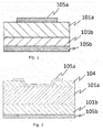
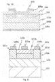
- Fig. 1 shows an example of a Schottky barrier diode (SBD) of the present invention.
- the SBD in Fig. 1 includes an n - -type semiconductor layer 101 a, an n + -type semiconductor layer 101 b, a Schottky electrode 105a, and an ohmic electrode 105b.
- the material of the Schottky and ohmic electrodes may be any electrode material known in the art.
- Examples of such an electrode material include metals, containing Al, Mo, Co, Zr, Sn, Nb, Fe, Cr, Ta, Ti, Au, Pt, V, Mn, Ni, Cu, Hf, W, Ir, Zn, In, Pd, Nd, and Ag, and alloys thereof, metal oxide conductive films such as tin oxide, zinc oxide, indium oxide, indium tin oxide (ITO), and indium zinc oxide (IZO), organic conductive compounds such as polyaniline, polythiophene, and polypyrrole, and mixtures of these materials.
- the Schottky and ohmic electrodes can be formed by known method such as a vacuum evaporation method or a sputtering method.
- a Schottky electrode can be formed by laminating a layer made from Mo and a layer made from Al and patterning these layers using photolithography.
- a depletion layer (not shown) expands in the n - -type semiconductor layer 101a, so that the SBD becomes a high-voltage SBD.
- a forward bias is applied, electrons flow from the ohmic electrode 105b to the Schottky electrode 105a.
- the SBD using the crystalline multilayer structure is excellent for high-voltage and large-current use and has a high switching speed, good withstand voltage characteristics, and high reliability.
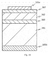
- Fig. 2 shows an example of a Schottky barrier diode (SBD) of the present invention.
- the SBD in Fig. 2 includes the elements of the SBD in Fig. 1 , as well as an insulator layer 104. More specifically, the SBD in Fig. 2 includes the n - -type semiconductor layer 101a, the n + -type semiconductor layer 101 b, the Schottky electrode 105a, the ohmic electrode 105b, and the insulator layer 104.
- the material of the insulator layer 104 is, for example, GaO, AlGaO, InAlGaO, AllnZnGaO4, AIN, Hf 2 O 3 , SiN, SiON, Al 2 O 3 , MgO, GdO, SiO 2 , or Si 3 N 4 , but in the present invention, is preferably a corundum-structured material.
- a corundum-structured insulator As the insulator layer, the semiconductor properties can be favorably exhibited on the interface.
- the insulator layer 104 is disposed between the n - -type semiconductor layer 101 a and the Schottky electrode 105a.
- the insulator layer can be formed by known method such as a sputtering method, a vacuum evaporation method, a CVD method or the like.
- the forming method, material, and the like of the Schottky and ohmic electrodes are the same as or similar to those of the SBD in Fig. 1 .
- the SBD in Fig. 2 has higher insulation properties and current controllability than the SBD in Fig. 1 .
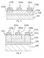
- Fig. 3 shows an example of a metal semiconductor field-effect transistor (MESFET) of the present invention.
- the MESFET in Fig. 3 includes an n - -type semiconductor layer 111a, an n + -type semiconductor layer 111b, a buffer layer 118, a semi-insulator layer 114, a gate electrode 115a, a source electrode 115b, and a drain electrode 115c.
- the material of the gate, drain, and source electrodes may be a known electrode material.
- Examples of such an electrode material include metals, containing Al, Mo, Co, Zr, Sn, Nb, Fe, Cr, Ta, Ti, Au, Pt, V, Mn, Ni, Cu, Hf, W, Ir, Zn, In, Pd, Nd, and Ag, and alloys thereof, metal oxide conductive films such as tin oxide, zinc oxide, indium oxide, indium tin oxide (ITO), and indium zinc oxide (IZO), organic conductive compounds such as polyaniline, polythiophene, and polypyrrole, and mixtures of these materials.
- the gate, drain, and source electrodes can be formed by known method such as a vacuum evaporation method, a sputtering method or the like.
- the semi-insulator layer 114 only has to be formed of a semi-insulator.
- the semi-insulator include those containing a semi-insulator dopant such as magnesium (Mg), ruthenium (Ru), iron (Fe), beryllium (Be), cesium (Cs), strontium, or barium and those which have not been doped.
- the MESFET in Fig. 3 has a favorable depletion layer formed under the gate electrode, there can be efficiently controlled the current flowing from the drain electrode to the source electrode.
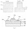
- Fig. 4 shows an example of a high-electron-mobility transistor (HEMT) of the present invention.
- the HEMT in Fig. 4 includes a wide-band-gap n-type semiconductor layer 121a, a narrow-band-gap n-type semiconductor layer 121b, an n + -type semiconductor layer 121c, a buffer layer 128, a semi-insulator layer 124, a gate electrode 125a, a source electrode 125b ,and a drain electrode 125c.
- HEMT high-electron-mobility transistor
- the materials of the gate, drain, and source electrodes may be known electrode materials.
- electrode materials include metals, containing Al, Mo, Co, Zr, Sn, Nb, Fe, Cr, Ta, Ti, Au, Pt, V, Mn, Ni, Cu, Hf, W, Ir, Zn, In, Pd, Nd, and Ag, and alloys thereof, metal oxide conductive films such as tin oxide, zinc oxide, indium oxide, indium tin oxide (ITO), and indium zinc oxide (IZO), organic conductive compounds such as polyaniline, polythiophene, and polypyrrole, and mixtures of these materials.
- the gate, drain, and source electrodes can be formed by known method such as a vacuum evaporation method, a sputtering method or the like.
- the n-type semiconductor layer under the gate electrode includes at least the wide-band-gap layer 121 a and the narrow-band-gap layer 121b.
- the semi-insulator layer 124 only has to be formed of a semi-insulator. Examples of the semi-insulator include those containing a semi-insulator dopant such as ruthenium (Ru) or iron (Fe) and those which have not been doped.
- the HEMT in Fig. 4 has a favorable depletion layer formed under the gate electrode, there can be efficiently controlled the current flowing from the drain electrode to the source electrode. Further, if this HEMT has a recess structure, the normally-off characteristics can be achieved.
- Fig. 5 shows an example of a MOSFET which is a semiconductor device of the present invention.
- the MOSFET in Fig. 5 is a trench MOSFET and includes an n - -type semiconductor layer 131 a, n + -type semiconductor layers 131b and 131c, a gate insulating film 134, a gate electrode 135a, a source electrode 135b, and a drain electrode 135c.
- n + -type semiconductor layer 131b having a thickness of, e.g., 100 nm to 100 ⁇ m is formed on the drain electrode 135c; an n - -type semiconductor layer 131 a having a thickness of, e.g., 100 nm to 100 ⁇ m is formed on the n + -type semiconductor layer 131b; the n + -type semiconductor layer 131 c is formed on the n - -type semiconductor layer 131 a; and the source electrode 135b is formed on the n + -type semiconductor layer 131c.
- the gate insulating film 134 having a thickness of, e.g., 10 nm to 1 ⁇ m and the gate electrode 135a are embedded in the trenches in this order.
- a channel layer is formed on a side of the n - -type semiconductor layer 131a, and electrons are injected into the n - -type semiconductor layer 131a.
- the MOSFET is turned on.
- the voltage of the gate electrode is set to 0 V, a formation of a channel layer is stopped, and the n - -type semiconductor layer 131 a is filled with the depletion layer.
- the MOSFET is turned off.
- Fig. 6 shows a part of a process of manufacturing the MOSFET in Fig. 5 .
- etching masks are disposed in predetermined regions of an n - -type semiconductor layer 131 a and an n + -type semiconductor layer 131c of a multilayer body as shown in Fig. 6A .
- anisotropic etching is performed by reactive ion etching or the like to form trenches which penetrate through the n + -type semiconductor layer 131c and halfway through the n - -type semiconductor layer 131a in the depth direction, as shown in Fig. 6B .
- a gate insulating film 134 having a thickness of, e.g., 50 nm to 1 ⁇ m is formed on side and bottom surfaces of the trenches using known method such as a thermal oxidation method, a vacuum evaporation method, a sputtering method, a CVD method or the like.
- a gate electrode material such as polysilicon is formed with a thickness smaller than or equal to that of the n - -type semiconductor layer 131a in the trenches by a CVD method, a vacuum evaporation method, a sputtering method, or the like.
- a source electrode 135b and a drain electrode 135c are formed on the n + -type semiconductor layer 131c and n + -type semiconductor layer 131b, respectively, by known method such as a vacuum evaporation method, a sputtering method, or a CVD method. In this way, a power MOSFET is manufactured.
- the materials of the source and drain electrodes may be known electrode materials.
- Examples of such electrode materials include metals, containing Al, Mo, Co, Zr, Sn, Nb, Fe, Cr, Ta, Ti, Au, Pt, V, Mn, Ni, Cu, Hf, W, Ir, Zn, In, Pd, Nd, and Ag, and alloys thereof, metal oxide conductive films such as tin oxide, zinc oxide, indium oxide, indium tin oxide (ITO), and indium zinc oxide (IZO), organic conductive compounds such as polyaniline, polythiophene, and polypyrrole, and mixtures of these materials.
- metals containing Al, Mo, Co, Zr, Sn, Nb, Fe, Cr, Ta, Ti, Au, Pt, V, Mn, Ni, Cu, Hf, W, Ir, Zn, In, Pd, Nd, and Ag, and alloys thereof, metal oxide conductive films such as tin oxide, zinc oxide, indium oxide, indium tin oxide (ITO), and indium zinc oxide (IZO), organic conductive compounds
- the MOSFET thus formed has better withstand voltage characteristics than conventional trench MOSFETs. While an example of a vertical trench MOSFET is shown in Fig. 5 , the present invention is not limited to this example and is applicable to various forms of MOSFETs. For example, the trenches in Fig. 5 may be dug to a depth such that they reach the bottom of the n - -type semiconductor layer 131 a, to reduce the series resistance. Further, an example of a lateral MOSFET is shown in Fig. 7 . The MOSFET in Fig.
- n - -type semiconductor layer 131a includes an n - -type semiconductor layer 131a, a first n + -type semiconductor layer 131b, a second n + -type semiconductor layer 131c, a gate insulating film 134, a gate electrode 135a, a source electrode 135b, a drain electrode 135c, a buffer layer 138, and a semi-insulator layer 139.
- the n + -type semiconductor layers are embedded in the n - -type semiconductor layer, so that the current can be passed more favorably.
- Fig. 8 shows an example of an SIT which is a semiconductor device of the present invention.
- the SIT in Fig. 8 includes an n - -type semiconductor layer 141 a, n + -type semiconductor layers 141 b and 141c, a gate electrode 145a, a source electrode 145b, and a drain electrode 145c.
- the n + -type semiconductor layer 141b having a thickness of, e.g., 100 nm to 100 ⁇ m is formed on the drain electrode 145c; the n - -type semiconductor layer 141a having a thickness of, e.g., 100 nm to 100 ⁇ m is formed on the n+-type semiconductor layer 141b; the n + -type semiconductor layer 141c is formed on the n - -type semiconductor layer 141a; and the source electrode 145b is formed on the n + -type semiconductor layer 141c.
- the gate electrode 145a is formed on the n - -type semiconductor layer 141a in the trenches.
- a voltage is applied between the source electrode 145b and the drain electrode 145c and thus a positive voltage is supplied to the gate electrode 145a through the source electrode 145b, a channel layer is formed within the n - -type semiconductor layer 141 a, and electrons are injected into the n - -type semiconductor layer 141a.
- the SIT is turned on.
- the voltage of the gate electrode is set to 0 V, a formation of a channel layer is stopped, and the n - -type semiconductor layer 141a is filled with the depletion layer.
- the SIT is turned off.
- Fig. 9 shows a part of a process of manufacturing the SIT in Fig. 8 .
- etching masks are disposed in predetermined regions of an n - -type semiconductor layer 141a and an n + -type semiconductor layer 141 c of a multilayer body as shown in Fig. 9A ; anisotropic etching is performed using reactive ion etching or the like to form trenches which penetrate through the n + -type semiconductor layer 141 c and halfway through the n - -type semiconductor layer 141a in the depth direction, as shown in Fig. 9B .
- a gate electrode material such as polysilicon is formed with a thickness smaller than or equal to that of the n - -type semiconductor layer 141a in the trenches by a CVD method, a vacuum evaporation method, a sputtering method, or the like.
- a source electrode 145b and drain electrode 145c are formed on the n + -type semiconductor layer 141c and n + -type semiconductor layer 141b, respectively, by known means such as vacuum evaporation, sputtering, CVD, or the like. In this way, a SIT is manufactured.
- the materials of the source and drain electrodes may be known electrode materials.
- Examples of such electrode materials include metals, containing Al, Mo, Co, Zr, Sn, Nb, Fe, Cr, Ta, Ti, Au, Pt, V, Mn, Ni, Cu, Hf, W, Ir, Zn, In, Pd, Nd, and Ag, and alloys thereof, metal oxide conductive films such as tin oxide, zinc oxide, indium oxide, indium tin oxide (ITO), and indium zinc oxide (IZO), organic conductive compounds such as polyaniline, polythiophene, and polypyrrole, and mixtures of these materials.
- metals containing Al, Mo, Co, Zr, Sn, Nb, Fe, Cr, Ta, Ti, Au, Pt, V, Mn, Ni, Cu, Hf, W, Ir, Zn, In, Pd, Nd, and Ag, and alloys thereof, metal oxide conductive films such as tin oxide, zinc oxide, indium oxide, indium tin oxide (ITO), and indium zinc oxide (IZO), organic conductive compounds
- a p-type semiconductor may be used in a semiconductor device.
- Figs. 10 to 16 show examples of a semiconductor device using a p-type semiconductor. These semiconductor devices can be manufactured in manners similar to those of the above examples.
- the p-type semiconductor may be one whose material is the same as that of an n-type semiconductor and which includes a p-type dopant or may be one whose material differs from that of an n-type semiconductor.
- Fig. 10 shows an preferred example of a Schottky barrier diode (SBD) including an n - -type semiconductor layer 101 a, an n + -type semiconductor layer 101b, a p-type semiconductor layer 102, a metal layer 103, an insulator layer 104, a Schottky electrode 105a, and an ohmic electrode 105b.
- the metal layer 103 formed from, for example, a metal such as Al and covers the Schottky electrode 105a.
- HEMT high-electron-mobility transistor
- a wide-band-gap n-type semiconductor layer 121 a a narrow-band-gap n-type semiconductor layer 121 b, an n + -type semiconductor layer 121 c, a p-type semiconductor layer 123, a gate electrode 125a, a source electrode 125b, a drain electrode 125c, and a substrate 129.
- HEMT high-electron-mobility transistor
- Fig. 12 shows a preferred example of a metal oxide semiconductor field-effect transistor (MOSFET) including an n - -type semiconductor layer 131 a, a first n + -type semiconductor layer 131b, a second n + -type semiconductor layer 131c, a p-type semiconductor layer 132, a p + -type semiconductor layer 132a, a gate insulating film 134, a gate electrode 135a, a source electrode 135b, and a drain electrode 135c.
- the p + -type semiconductor layer 132a may be a p-type semiconductor layer or may be the same as the p-type semiconductor layer 132.
- JFET junction field-effect transistor
- IGBT insulated gate bipolar transistor
- Fig. 15 shows an example of a light-emitting diode (LED) which is a semiconductor device of the present invention.
- LED light-emitting diode
- an n-type semiconductor layer 161 is disposed on a second electrode 165b, and a light-emitting layer 163 is laminated on the n-type semiconductor layer 161.
- a p-type semiconductor layer 162 is laminated on the light-emitting layer 163.
- a translucent electrode 167 configured to transmit light emitted by the light-emitting layer 163 is disposed on the p-type semiconductor layer 162.
- a first electrode 165a is laminated on the translucent electrode 167. Note that the semiconductor light-emitting device in Fig. 15 may be covered by a protective layer except for the electrodes thereof.
- Examples of the material of the translucent electrode include conductive oxide materials containing indium (In) or titanium (Ti). More specific examples include In 2 O 3 , ZnO, SnO 2 , Ga 2 O 3 , TiO 2 , CeO 2 , mixed crystals of two or more thereof, and doped ones of these materials.
- the translucent electrode can be formed from the above materials by known means such as sputtering. The formed translucent electrode may be thermally annealed to provide it with transparency.
- the light-emitting layer 163 when a current is passed through the p-type semiconductor layer 162, the light-emitting layer 163, and the n-type semiconductor layer 161 while using the first electrode 165a as a positive electrode and the second electrode 165b as a negative electrode, the light-emitting layer 163 emits light.
- Examples of the material of the first electrode 165a and the second electrode 165b include metals, containing Al, Mo, Co, Zr, Sn, Nb, Fe, Cr, Ta, Ti, Au, Pt, V, Mn, Ni, Cu, Hf, W, Ir, Zn, In, Pd, Nd, and Ag, and alloys thereof, metal oxide conductive films such as tin oxide, zinc oxide, indium oxide, indium tin oxide (ITO), and indium zinc oxide (IZO), organic conductive compounds such as polyaniline, polythiophene, and polypyrrole, and mixtures of these materials.
- metals containing Al, Mo, Co, Zr, Sn, Nb, Fe, Cr, Ta, Ti, Au, Pt, V, Mn, Ni, Cu, Hf, W, Ir, Zn, In, Pd, Nd, and Ag, and alloys thereof, metal oxide conductive films such as tin oxide, zinc oxide, indium oxide, indium tin oxide (ITO),
- the method for forming the electrode is not particularly limited, and it is possible to form using any film-forming method and, for example, may be formed on the substrate using a method which is appropriately selected from among wet methods such as printing, spraying, and coating, physical methods such as vacuum evaporation, sputtering, and ion plating, chemical methods such as CVD and plasma CVD, and the like considering the suitability for the electrode material.
- Fig. 16 shows another form of light-emitting device.
- an n-type semiconductor layer 161 is laminated on a substrate 169, and a second electrode 165b is laminated on a part of a surface of the n-type semiconductor layer 161 exposed by cutting off respective parts of a p-type semiconductor layer 162, a light-emitting layer 163, and the n-type semiconductor layer 161.
- the CVD apparatus 19 includes a sample stage 21 for placing a sample 20 on which films are to be formed, such as a base substrate, a carrier-gas source 22 for providing a carrier gas, a flow rate control valve 23 for controlling the flow rate of the carrier gas sent from the carrier-gas source 22, a mist source 24 containing a raw-material solution 24a, a container 25 containing water 25a, an ultrasonic transducer 26 attached to the bottom of the container 25, a film forming chamber 27 formed of a 40-mm-inner-diameter quartz tube, and a heater 28 disposed around the film forming chamber 27.
- the sample stage 21 is formed of quartz, and the surface thereof for placing the sample 20 is inclined from the horizontal plane. By forming both the film forming chamber 27 and sample stage 21 from quartz, entry of apparatus-derived impurities into films formed on the sample 20 is reduced.
- An aqueous solution was prepared from gallium bromide and germanium oxide such that the atomic ratio of germanium to gallium was 1:0.05. Then, a 48% solution of hydrobromic acid was added to the aqueous solution at a volume percent of 10%. In condition 1, the concentration of germanium oxide was set to 5.0 ⁇ 10 -3 mol/L.
- An aqueous solution was prepared such that the molar ratio among gallium bromide, aluminum bromide, and germanium oxide was 100:200:0.04. Then, a 48% solution of hydrobromic acid was added to the aqueous solution at a volume percent of 10%. In condition 2, the concentration of germanium oxide was set to 4.0 ⁇ 10 -5 mol/L.
- the raw-material solution 24a thus prepared was injected into the mist source 24.
- a 10 mm-side square, 600 ⁇ m-thick c-plane sapphire substrate was placed as the sample 20 on the sample stage 21, and the heater 28 was activated to raise the temperature in the film forming chamber 27 to 500°C.
- the flow rate control valve 23 was opened to send the carrier gas from the carrier-gas source 22 into the film forming chamber 27.
- the flow rate of the carrier gas was adjusted to 5 L/min.
- An oxygen gas was used as the carrier gas.
- the ultrasonic transducer 26 was vibrated at 2.4 MHz so that the vibration was propagated to the raw-material solution 24a through the water 25a.
- the raw-material solution 24a was atomized into raw-material fine particles.
- the raw-material fine particles were carried into the film forming chamber 27 by the carrier gas and then the thin film was formed by a CVD reaction on the film forming surface of the sample 20.
- the sample thin film formed under condition 1 was annealed using a mixed gas of hydrogen and nitrogen (mixture ratio of 5:95) at 800°C for 90 minutes.
- the phases of the respective thin films formed under conditions 1 and 2 were identified. The identification was made by 2 ⁇ / ⁇ scanning each thin film at angles of 15 to 95 degrees using an XRD diffractometer for thin films. Then, measurements were made using CuK ⁇ rays. As a result, the thin film formed from the raw-material solution of condition 1 was found to be an ⁇ -Ga 2 O 3 thin film. On the other hand, while the thin film formed from the raw-material solution of condition 2 was an ⁇ -Ga 2 O 3 thin film before annealed, it was believed to have been transformed into a microcrystalline or an amorphous Ga 2 O 3 thin film by annealing.
- Table 1 indicates that both the thin films of conditions 1 and 2 were provided with electrical conductivity. Note that for condition 2, the annealed thin film was measured. [Table 1] Condition 1 Condition 2 Hall coefficient 1.22E+00 6.19E-01 [cm 3 /C] Carrier concentration 5.10E+18 1.01E+19 [1/cm 3 ] Sheet carrier concentration 2.55E+14 5.04E+14 [1/cm 2 ] Mobility 2.60E-01 3.26E+00 [cm 2 /V*s]
- tin-doped experiments a solution obtained by dissolving tin (II) chloride dihydrate, gallium acetylacetonate, and hydrochloric acid in water was used as a raw material.
- germanium-doped experiments the condition was the same as that in condition 1 except that the amount of germanium oxide was changed.
- Raw-material solutions containing different amounts of tin or germanium were prepared and then films were formed from the respective raw-material solutions at 500°C and at a flow rate of 5L/min using oxygen as a carrier gas for 30 minutes.
- Table 2 blow shows the results.
- films whose resistance value was 1.0E+10 ⁇ or less are rated as “low resistance,” and films whose resistance value was more than 1.0E+10 ⁇ are rated as “high resistance.”
- the "in-solution dopant content” refers to the molar percentage of germanium to gallium in the raw-material solution.
- the thin films doped with tin at high concentrations of 1% or more exhibited no electrical conductivity. This means that a high-concentration doped layer for use in ohmic connection with the electrode is difficult to form. Accordingly, these thin films are problematic in terms of industrial applications.
- Raw-material solutions were prepared from gallium bromide and germanium oxide such that the atomic ratio of germanium to gallium is 1 E-7, 1 E-6, 8E-5, 4E-4, 2E-3, 1 E-2, 2E-1, and 8E-1, respectively. Then, a 48% solution of hydrobromic acid was added to each raw-material solution at a volume percent of 10%. Then, thin films were formed from these raw-material solutions under the above conditions, and the concentration of the impurity was analyzed quantitatively using an SIMS under the following conditions: incident ion species oxygen; and output 3kV, 200 nA. The results are shown in Fig. 18.
- Fig. 18 indicates that the in-solution dopant content and the in-film dopant content have a correlation and that by adjusting the in-solution dopant content, the dopant content of a thin film to be formed can be easily controlled.
- a Ge-doped thin film sample was formed from a raw-material solution having a Ge concentration of 0.04% (this thin film will be referred to as the Example sample) in a manner similar to condition 1. Further, a Sn-doped thin film sample was formed from a raw-material solution having a Sn concentration of 0.04% using a film forming method disclosed in Non-Patent Literature 3 ( Electrical Conductive Corundum-Structured ⁇ -Ga2O3 Thin Films on Sapphire with Tin-Doping Grown by Spray-Assisted Mist Chemical Vapor Deposition, Japanese Journal ofApplied Physics 51 (2012) 070203 ) (this thin film will be referred to as the reference sample).
- Fig. 19 indicates that while the Sn-doped thin film increased in the resistance value, the Ge-doped thin film decreased in resistance value. Specifically, when the Sn-doped gallium oxide thin film was annealed in the formation of an ohmic electrode, it increased in the resistance; the Ge-doped gallium oxide thin film avoided increasing in resistance. Accordingly, the latter seems to be advantageous in achieving an ohmic contact.
- An aqueous solution was prepared such that the molar ratio among gallium bromide and germanium oxide was 100: 5. Then, a 48% solution of hydrobromic acid was added to the aqueous solution at a volume percent of 10%. The concentration of germanium oxide was set to 5.0 ⁇ 10 -3 mol/L. Then, a film was formed from the aqueous solution at 500°C and at a flow rate of 5L/min using nitrogen as a carrier gas for 30 minutes.
- An aqueous solution was prepared such that the molar ratio among gallium bromide and tin bromide was 100: 1. Then, a 48% solution of hydrobromic acid was added to the aqueous solution at a volume percent of 10%. The concentration of tin bromide was set to 1.0 ⁇ 10 -3 mol/L. Then, a film was formed from the aqueous solution at 500°C and at a flow rate of 5L/min using nitrogen as a carrier gas for 30 minutes.
- the thin film samples formed under conditions 3 and 4 were SIMS measured using ADEPT-1010 manufactured by ULVAC PHI under the following conditions: incident ion species Cs; and output 3 kV, 100 nA.
- the signal strength of each ion species was divided by the signal strength of oxygen (180), and the value obtained was averaged in the depth direction.
- the values obtained are shown in Table 3. It can be said that as the signal strength becomes weaker, the amount of impurity becomes smaller.
- Table 3 indicates that while the reference sample of condition 4 contained large amounts of carbon and chloride as contamination, the Example sample of condition 3 was substantially free of carbon or chloride contamination, as well as had an effect of suppressing hydrogen or nitride contamination.
- An aqueous solution was prepared such that the molar ratio among gallium bromide, and tetraethyl orthosilicate was 100: 1. Then, a 48% solution of hydrobromic acid was added to the aqueous solution at a volume percent of 10%. The concentration of tetraethyl orthosilicate was set to 1.0 ⁇ 10 -3 mol/L. Then, a film was formed from the aqueous solution at 500°C and at a flow rate of 5L/min using nitrogen as a carrier gas for 30 minutes. As a result, this sample was found to exhibit performance equivalent to that of the germanium-doped Example sample.
- An aqueous solution was prepared such that the molar ratio among gallium bromide and titanium acetylacetonate was 100: 1. Then, a 48% solution of hydrobromic acid was added to the aqueous solution at a volume percent of 10%. The concentration of titanium acetylacetonate was set to 1.0 ⁇ 10 -3 mol/L. Then, a film was formed from the aqueous solution at 500°C and at a flow rate of 5L/min using nitrogen as a carrier gas for 30 minutes. As a result, this sample was found to exhibit performance equivalent to that of the germanium-containing Example sample and to have better electrical properties than the Sn-doped reference sample.
- An aqueous solution was prepared such that the molar ratio among gallium bromide and niobium bromide was 100: 1. Then, a 48% solution of hydrobromic acid was added to the aqueous solution at a volume percent of 10%. The concentration of niobium bromide was set to 1.0 ⁇ 10 -3 mol/L. Then, a film was formed from the aqueous solution at 500°C and at a flow rate of 5L/min using nitrogen as a carrier gas for 30 minutes. As a result, this sample was found to exhibit performance equivalent to that of the germanium-doped Example sample and to have better electrical properties than the Sn-doped reference sample.
- aqueous solution was prepared such that the molar ratio among gallium bromide and zirconium tetrachloride was 100: 1. Then, a 48% solution of hydrobromic acid was added to the aqueous solution at a volume percent of 10%. The concentration of zirconium tetrachloride was set to 1.0 ⁇ 10 -3 mol/L. Then, a film was formed from the aqueous solution at 500°C and at a flow rate of 5L/min using nitrogen as a carrier gas for 30 minutes. As a result, this sample was found to exhibit performance equivalent to that of the germanium-doped Example sample and to have better electrical properties than the Sn-doped reference sample.
- An aqueous solution was prepared such that the molar ratio among gallium bromide and vanadium bromide was 100: 1. Then, a 48% solution of hydrobromic acid was added to the aqueous solution at a volume percent of 10%. The concentration of vanadium bromide was set to 1.0 ⁇ 10 -3 mol/L. Then, a film was formed from the aqueous solution at 500°C and at a flow rate of 5L/min using nitrogen as a carrier gas for 30 minutes. As a result, this sample was found to exhibit performance equivalent to that of the germanium-doped Example sample and to have better electrical properties than the Sn-doped reference sample.
- a crystalline multilayer structure was formed under the following conditions: amount of indium 0.025 mol%L; amount of dopant 1 mol% relative to indium; carrier gas N 2 ; temperature 500°C; film-forming time 20 minutes; and other conditions the same as condition 1.
- a germanium-doped ⁇ -Ga 2 O 3 thin film was formed as an n + -type semiconductor layer on a c-plane sapphire substrate under the same condition as Condition 1, except that the concentration of the germanium oxide was set to 1.0 ⁇ 10 -3 mol/L in place of 5.0x10 -3 mol/L. Then, a non-doped ⁇ -Ga 2 O 3 thin film was formed as an n - -type semiconductor layer on the n + -type semiconductor layer unintentionally. This n - -type semiconductor layer was formed as described above except that the n - -type semiconductor layer was not doped. Then, as shown in Fig.
- an ohmic electrode consisting of Ti and a Schottky electrode consisting of Pt were formed on the n + -type semiconductor layer and n - -type semiconductor layer, respectively, by sputtering, thereby forming an SBD.
- FIG. 21 A SIMS analysis (Cs, 3kV, 200nA, Ap16%, Raster400) of the SBD thus formed was performed. The results are shown in Fig. 21 .
- the horizontal axis of Fig. 21 represents the time which elapsed since the start of sputtering. This graph indicates that while no germanium was contained until about 1500 seconds elapsed, germanium was contained uniformly during a period from when about 1500 seconds elapsed to when about 4000 seconds elapsed. This means that the n + -type semiconductor layer and n - -type semiconductor layer were favorably formed.
- a crystalline multilayer structure was obtained in the same as in condition 1 except that a c-plane sapphire substrate having an off-angle of 4 degrees was used as the substrate.
- the crystalline multilayer structure of the present invention can be used in all fields, including semiconductors (e.g., compound semiconductor electronic devices), electronic components/electric apparatus components, optical/electronic photograph-related devices, and industrial members. Since this crystalline multilayer structure has good semiconductor properties, it is particularly useful for semiconductor devices.
Applications Claiming Priority (1)
| Application Number | Priority Date | Filing Date | Title |
|---|---|---|---|
| JP2014097244 | 2014-05-08 |
Publications (2)
| Publication Number | Publication Date |
|---|---|
| EP2942803A1 true EP2942803A1 (de) | 2015-11-11 |
| EP2942803B1 EP2942803B1 (de) | 2019-08-21 |
Family
ID=52146230
Family Applications (1)
| Application Number | Title | Priority Date | Filing Date |
|---|---|---|---|
| EP14199100.0A Active EP2942803B1 (de) | 2014-05-08 | 2014-12-19 | Kristalline mehrschichtige Struktur und Halbleiterbauelement |
Country Status (5)
| Country | Link |
|---|---|
| US (1) | US9379190B2 (de) |
| EP (1) | EP2942803B1 (de) |
| JP (2) | JP6557899B2 (de) |
| CN (3) | CN110620145A (de) |
| TW (1) | TWI607511B (de) |
Cited By (4)
| Publication number | Priority date | Publication date | Assignee | Title |
|---|---|---|---|---|
| EP3190608A4 (de) * | 2014-09-02 | 2017-07-26 | Flosfia Inc. | Laminierte struktur, verfahren zur herstellung davon, halbleiterbauelement und kristalliner film |
| EP3301725A1 (de) * | 2016-10-03 | 2018-04-04 | Flosfia Inc. | Halbleiterbauelement und halbleiteranordnung mit halbleiterbauelement |
| CN111106167A (zh) * | 2019-11-27 | 2020-05-05 | 太原理工大学 | 一种择优取向的Ga2O3和SnO2混相膜基传感器的制备方法 |
| US11758745B2 (en) | 2019-04-18 | 2023-09-12 | Semiconductor Energy Laboratory Co., Ltd. | Solid-state relay and semiconductor device |
Families Citing this family (44)
| Publication number | Priority date | Publication date | Assignee | Title |
|---|---|---|---|---|
| US9379190B2 (en) * | 2014-05-08 | 2016-06-28 | Flosfia, Inc. | Crystalline multilayer structure and semiconductor device |
| CN108899359A (zh) * | 2014-07-22 | 2018-11-27 | Flosfia 株式会社 | 结晶性半导体膜和板状体以及半导体装置 |
| TWI667792B (zh) * | 2015-12-18 | 2019-08-01 | 日商Flosfia股份有限公司 | Semiconductor device |
| JP6906217B2 (ja) * | 2015-12-18 | 2021-07-21 | 株式会社Flosfia | 半導体装置 |
| JP2017128492A (ja) * | 2016-01-15 | 2017-07-27 | 株式会社Flosfia | 結晶性酸化物膜 |
| US10158029B2 (en) * | 2016-02-23 | 2018-12-18 | Analog Devices, Inc. | Apparatus and methods for robust overstress protection in compound semiconductor circuit applications |
| JP6705962B2 (ja) * | 2016-06-03 | 2020-06-03 | 株式会社タムラ製作所 | Ga2O3系結晶膜の成長方法及び結晶積層構造体 |
| DE112017003754B4 (de) * | 2016-07-26 | 2022-10-13 | Mitsubishi Electric Corporation | Halbleitervorrichtung und verfahren zum herstellen einer halbleitervorrichtung |
| JP6932904B2 (ja) * | 2016-08-24 | 2021-09-08 | 株式会社Flosfia | 半導体装置 |
| US10804362B2 (en) | 2016-08-31 | 2020-10-13 | Flosfia Inc. | Crystalline oxide semiconductor film, crystalline oxide semiconductor device, and crystalline oxide semiconductor system |
| WO2018052097A1 (ja) | 2016-09-15 | 2018-03-22 | 株式会社Flosfia | 半導体膜の製造方法及び半導体膜並びにドーピング用錯化合物及びドーピング方法 |
| JP2018067672A (ja) | 2016-10-21 | 2018-04-26 | 株式会社ブイ・テクノロジー | 酸化物半導体装置及びその製造方法 |
| EP3536828A4 (de) | 2016-11-07 | 2020-07-15 | Flosfia Inc. | Kristalline oxidhalbleiterschicht und halbleiterbauelement |
| JP7116409B2 (ja) * | 2017-02-27 | 2022-08-10 | 株式会社タムラ製作所 | トレンチmos型ショットキーダイオード |
| JP6967238B2 (ja) * | 2017-02-28 | 2021-11-17 | 株式会社タムラ製作所 | ショットキーバリアダイオード |
| JP2019007048A (ja) * | 2017-06-23 | 2019-01-17 | トヨタ自動車株式会社 | 成膜装置 |
| CN107293511B (zh) * | 2017-07-05 | 2019-11-12 | 京东方科技集团股份有限公司 | 一种膜层退火设备及退火方法 |
| CN107464844A (zh) * | 2017-07-20 | 2017-12-12 | 中国电子科技集团公司第十三研究所 | 氧化镓场效应晶体管的制备方法 |
| JP7166522B2 (ja) * | 2017-08-21 | 2022-11-08 | 株式会社Flosfia | 結晶膜の製造方法 |
| JP7065440B2 (ja) * | 2017-09-04 | 2022-05-12 | 株式会社Flosfia | 半導体装置の製造方法および半導体装置 |
| GB2601276B (en) * | 2017-12-11 | 2022-09-28 | Pragmatic Printing Ltd | Schottky diode |
| GB2569196B (en) | 2017-12-11 | 2022-04-20 | Pragmatic Printing Ltd | Schottky diode |
| CN108493234A (zh) * | 2018-05-10 | 2018-09-04 | 广东省半导体产业技术研究院 | 一种鳍式沟道的氧化镓基垂直场效应晶体管及其制备方法 |
| TW202018819A (zh) * | 2018-07-12 | 2020-05-16 | 日商Flosfia股份有限公司 | 半導體裝置和半導體系統 |
| TW202013716A (zh) * | 2018-07-12 | 2020-04-01 | 日商Flosfia股份有限公司 | 半導體裝置和半導體系統 |
| TW202006945A (zh) * | 2018-07-12 | 2020-02-01 | 日商Flosfia股份有限公司 | 半導體裝置和半導體系統 |
| JP7404594B2 (ja) * | 2018-07-12 | 2023-12-26 | 株式会社Flosfia | 半導体装置および半導体装置を含む半導体システム |
| JP2020011859A (ja) * | 2018-07-17 | 2020-01-23 | トヨタ自動車株式会社 | 成膜方法、及び、半導体装置の製造方法 |
| JP2020011858A (ja) * | 2018-07-17 | 2020-01-23 | トヨタ自動車株式会社 | 成膜方法、及び、半導体装置の製造方法 |
| KR102415439B1 (ko) * | 2018-08-01 | 2022-06-30 | 이데미쓰 고산 가부시키가이샤 | 결정 구조 화합물, 산화물 소결체, 스퍼터링 타깃, 결정질 산화물 박막, 아모르퍼스 산화물 박막, 박막 트랜지스터, 및 전자 기기 |
| JP6857641B2 (ja) | 2018-12-19 | 2021-04-14 | 信越化学工業株式会社 | 成膜方法及び成膜装置 |
| JP7315136B2 (ja) * | 2018-12-26 | 2023-07-26 | 株式会社Flosfia | 結晶性酸化物半導体 |
| JP7086270B2 (ja) * | 2019-03-13 | 2022-06-17 | 三菱電機株式会社 | 半導体装置 |
| WO2020204006A1 (ja) | 2019-03-29 | 2020-10-08 | 株式会社Flosfia | 結晶、結晶性酸化物半導体、結晶性酸化物半導体を含む半導体膜、結晶および/または半導体膜を含む半導体装置および半導体装置を含むシステム |
| JP7409790B2 (ja) * | 2019-06-20 | 2024-01-09 | 信越化学工業株式会社 | 酸化物半導体膜及び半導体装置 |
| CN110571152A (zh) * | 2019-08-14 | 2019-12-13 | 青岛佳恩半导体有限公司 | 一种igbt背面电极缓冲层的制备方法 |
| JP7128970B2 (ja) * | 2019-08-27 | 2022-08-31 | 信越化学工業株式会社 | 積層構造体及び積層構造体の製造方法 |
| TW202129095A (zh) * | 2019-09-30 | 2021-08-01 | 日商Flosfia股份有限公司 | 積層結構體及半導體裝置 |
| CN110752159B (zh) * | 2019-10-28 | 2023-08-29 | 中国科学技术大学 | 对氧化镓材料退火的方法 |
| CN114930501A (zh) * | 2020-01-10 | 2022-08-19 | 株式会社Flosfia | 导电性金属氧化膜、半导体元件和半导体装置 |
| JPWO2022009970A1 (de) * | 2020-07-10 | 2022-01-13 | ||
| JP7469201B2 (ja) * | 2020-09-18 | 2024-04-16 | 株式会社デンソー | 半導体装置とその製造方法 |
| KR102394975B1 (ko) * | 2020-10-22 | 2022-05-09 | 경북대학교 산학협력단 | 반도체 소자의 제조 방법 및 이에 의해 제조된 반도체 소자 |
| WO2022230831A1 (ja) * | 2021-04-26 | 2022-11-03 | 株式会社Flosfia | 半導体装置 |
Citations (5)
| Publication number | Priority date | Publication date | Assignee | Title |
|---|---|---|---|---|
| JP2009081359A (ja) | 2007-09-27 | 2009-04-16 | National Institute Of Advanced Industrial & Technology | 不純物イオン注入層の電気的活性化方法 |
| JP2013028480A (ja) | 2011-07-27 | 2013-02-07 | Kochi Univ Of Technology | ドーパントを添加した結晶性の高い導電性α型酸化ガリウム薄膜およびその生成方法 |
| WO2013035843A1 (ja) * | 2011-09-08 | 2013-03-14 | 株式会社タムラ製作所 | Ga2O3系半導体素子 |
| JP2013058637A (ja) | 2011-09-08 | 2013-03-28 | Tamura Seisakusho Co Ltd | Ga2O3系半導体素子 |
| WO2014050793A1 (ja) * | 2012-09-28 | 2014-04-03 | Roca株式会社 | 半導体装置又は結晶、および、半導体装置又は結晶の製造方法 |
Family Cites Families (14)
| Publication number | Priority date | Publication date | Assignee | Title |
|---|---|---|---|---|
| WO2010067525A1 (ja) * | 2008-12-08 | 2010-06-17 | 住友化学株式会社 | 半導体装置、半導体装置の製造方法、半導体基板、および半導体基板の製造方法 |
| KR101932576B1 (ko) * | 2010-09-13 | 2018-12-26 | 가부시키가이샤 한도오따이 에네루기 켄큐쇼 | 반도체 장치 및 그 제작 방법 |
| KR101895398B1 (ko) * | 2011-04-28 | 2018-10-25 | 삼성전자 주식회사 | 산화물 층의 형성 방법 및 이를 포함하는 반도체 소자의 제조 방법 |
| KR101952570B1 (ko) * | 2011-05-13 | 2019-02-27 | 가부시키가이샤 한도오따이 에네루기 켄큐쇼 | 반도체 장치 및 그 제작 방법 |
| JP6013685B2 (ja) * | 2011-07-22 | 2016-10-25 | 株式会社半導体エネルギー研究所 | 半導体装置 |
| WO2013069729A1 (ja) * | 2011-11-09 | 2013-05-16 | 株式会社タムラ製作所 | 半導体素子及びその製造方法 |
| JP6450675B2 (ja) * | 2012-06-14 | 2019-01-09 | ティブラ コーポレーションTivra Corporation | 多層基板構造を形成する方法 |
| JP5972065B2 (ja) * | 2012-06-20 | 2016-08-17 | 富士フイルム株式会社 | 薄膜トランジスタの製造方法 |
| SG11201505225TA (en) * | 2012-08-03 | 2015-08-28 | Semiconductor Energy Lab | Oxide semiconductor stacked film and semiconductor device |
| CN103117226B (zh) * | 2013-02-04 | 2015-07-01 | 青岛大学 | 一种合金氧化物薄膜晶体管的制备方法 |
| JP5397794B1 (ja) * | 2013-06-04 | 2014-01-22 | Roca株式会社 | 酸化物結晶薄膜の製造方法 |
| JP5397795B1 (ja) * | 2013-06-21 | 2014-01-22 | Roca株式会社 | 半導体装置及びその製造方法、結晶及びその製造方法 |
| US10109707B2 (en) * | 2014-03-31 | 2018-10-23 | Flosfia Inc. | Crystalline multilayer oxide thin films structure in semiconductor device |
| US9379190B2 (en) * | 2014-05-08 | 2016-06-28 | Flosfia, Inc. | Crystalline multilayer structure and semiconductor device |
-
2014
- 2014-12-19 US US14/577,986 patent/US9379190B2/en active Active
- 2014-12-19 EP EP14199100.0A patent/EP2942803B1/de active Active
-
2015
- 2015-05-07 JP JP2015095288A patent/JP6557899B2/ja active Active
- 2015-05-08 CN CN201910915606.0A patent/CN110620145A/zh active Pending
- 2015-05-08 CN CN201910353479.XA patent/CN110047907B/zh active Active
- 2015-05-08 TW TW104114709A patent/TWI607511B/zh active
- 2015-05-08 CN CN201510232391.4A patent/CN105097957A/zh active Pending
-
2019
- 2019-03-20 JP JP2019053236A patent/JP6893625B2/ja active Active
Patent Citations (5)
| Publication number | Priority date | Publication date | Assignee | Title |
|---|---|---|---|---|
| JP2009081359A (ja) | 2007-09-27 | 2009-04-16 | National Institute Of Advanced Industrial & Technology | 不純物イオン注入層の電気的活性化方法 |
| JP2013028480A (ja) | 2011-07-27 | 2013-02-07 | Kochi Univ Of Technology | ドーパントを添加した結晶性の高い導電性α型酸化ガリウム薄膜およびその生成方法 |
| WO2013035843A1 (ja) * | 2011-09-08 | 2013-03-14 | 株式会社タムラ製作所 | Ga2O3系半導体素子 |
| JP2013058637A (ja) | 2011-09-08 | 2013-03-28 | Tamura Seisakusho Co Ltd | Ga2O3系半導体素子 |
| WO2014050793A1 (ja) * | 2012-09-28 | 2014-04-03 | Roca株式会社 | 半導体装置又は結晶、および、半導体装置又は結晶の製造方法 |
Non-Patent Citations (3)
| Title |
|---|
| "Electrical Conductive Corundum-Structured a-Ga 0 Thin Films on Sapphire with Tin-Doping Grown by Spray-Assisted Mist Chemical Vapor Deposition", JAPANESE JOURNAL OF APPLIED PHYSICS, vol. 51, 2012, pages 070203 |
| JUN LIANG ZHAO ET AL.: "UV and Visible Electroluminescence From a Sn: Ga 0 /n+-Si Heterojunction by Metal-Organic Chemical Vapor Deposition", IEEE TRANSACTIONS ON ELECTRON DEVICES, vol. 58, no. 5, May 2011 (2011-05-01) |
| KOHEI SASAKI ET AL.: "Si-lon Implantation Doping in ?-Ga O and Its Application to Fabrication of Low-Resistance Ohmic Contacts", APPLIED PHYSICS EXPRESS, vol. 6, 2013, pages 086502 |
Cited By (7)
| Publication number | Priority date | Publication date | Assignee | Title |
|---|---|---|---|---|
| EP3190608A4 (de) * | 2014-09-02 | 2017-07-26 | Flosfia Inc. | Laminierte struktur, verfahren zur herstellung davon, halbleiterbauelement und kristalliner film |
| US10043664B2 (en) | 2014-09-02 | 2018-08-07 | Flosfia Inc. | Multilayer structure, method for manufacturing same, semiconductor device, and crystalline film |
| EP3783662A1 (de) * | 2014-09-02 | 2021-02-24 | Flosfia Inc. | Laminierte struktur, verfahren zur herstellung davon, halbleiterbauelement und kristalliner film |
| EP3301725A1 (de) * | 2016-10-03 | 2018-04-04 | Flosfia Inc. | Halbleiterbauelement und halbleiteranordnung mit halbleiterbauelement |
| CN107895742A (zh) * | 2016-10-03 | 2018-04-10 | 流慧株式会社 | 半导体装置以及包括半导体装置的半导体系统 |
| US11758745B2 (en) | 2019-04-18 | 2023-09-12 | Semiconductor Energy Laboratory Co., Ltd. | Solid-state relay and semiconductor device |
| CN111106167A (zh) * | 2019-11-27 | 2020-05-05 | 太原理工大学 | 一种择优取向的Ga2O3和SnO2混相膜基传感器的制备方法 |
Also Published As
| Publication number | Publication date |
|---|---|
| US9379190B2 (en) | 2016-06-28 |
| JP6893625B2 (ja) | 2021-06-23 |
| TW201543581A (zh) | 2015-11-16 |
| EP2942803B1 (de) | 2019-08-21 |
| JP6557899B2 (ja) | 2019-08-14 |
| TWI607511B (zh) | 2017-12-01 |
| CN110047907B (zh) | 2024-03-15 |
| CN105097957A (zh) | 2015-11-25 |
| JP2019142764A (ja) | 2019-08-29 |
| JP2015228495A (ja) | 2015-12-17 |
| CN110620145A (zh) | 2019-12-27 |
| US20150325659A1 (en) | 2015-11-12 |
| CN110047907A (zh) | 2019-07-23 |
Similar Documents
| Publication | Publication Date | Title |
|---|---|---|
| EP2942803B1 (de) | Kristalline mehrschichtige Struktur und Halbleiterbauelement | |
| JP6936982B2 (ja) | 半導体装置 | |
| US10535728B2 (en) | Crystalline multilayer oxide thin films structure in semiconductor device | |
| JP6916426B2 (ja) | 積層構造体およびその製造方法、半導体装置ならびに結晶膜 | |
| US11038026B2 (en) | Crystalline multilayer structure and semiconductor device | |
| US20190305091A1 (en) | Crystalline oxide semiconductor film and semiconductor device | |
| US20230223446A1 (en) | Laminate, semiconductor device, and method for manufacturing laminate | |
| JP6230196B2 (ja) | 結晶性半導体膜および半導体装置 | |
| JP6478425B2 (ja) | 結晶性半導体膜および半導体装置 |
Legal Events
| Date | Code | Title | Description |
|---|---|---|---|
| PUAI | Public reference made under article 153(3) epc to a published international application that has entered the european phase |
Free format text: ORIGINAL CODE: 0009012 |
|
| 17P | Request for examination filed |
Effective date: 20150118 |
|
| AK | Designated contracting states |
Kind code of ref document: A1 Designated state(s): AL AT BE BG CH CY CZ DE DK EE ES FI FR GB GR HR HU IE IS IT LI LT LU LV MC MK MT NL NO PL PT RO RS SE SI SK SM TR |
|
| AX | Request for extension of the european patent |
Extension state: BA ME |
|
| STAA | Information on the status of an ep patent application or granted ep patent |
Free format text: STATUS: EXAMINATION IS IN PROGRESS |
|
| 17Q | First examination report despatched |
Effective date: 20170425 |
|
| REG | Reference to a national code |
Ref country code: DE Ref legal event code: R079 Ref document number: 602014052072 Country of ref document: DE Free format text: PREVIOUS MAIN CLASS: H01L0021020000 Ipc: H01L0029660000 |
|
| RIC1 | Information provided on ipc code assigned before grant |
Ipc: H01L 29/739 20060101ALI20190205BHEP Ipc: H01L 33/26 20100101ALI20190205BHEP Ipc: H01L 29/812 20060101ALI20190205BHEP Ipc: H01L 29/66 20060101AFI20190205BHEP Ipc: H01L 29/04 20060101ALI20190205BHEP Ipc: H01L 33/42 20100101ALI20190205BHEP Ipc: H01L 29/78 20060101ALI20190205BHEP Ipc: H01L 29/808 20060101ALI20190205BHEP Ipc: H01L 29/772 20060101ALI20190205BHEP Ipc: H01L 29/10 20060101ALI20190205BHEP Ipc: H01L 29/24 20060101ALI20190205BHEP Ipc: H01L 29/872 20060101ALI20190205BHEP Ipc: H01L 21/02 20060101ALI20190205BHEP Ipc: H01L 29/06 20060101ALI20190205BHEP Ipc: H01L 29/778 20060101ALI20190205BHEP |
|
| GRAP | Despatch of communication of intention to grant a patent |
Free format text: ORIGINAL CODE: EPIDOSNIGR1 |
|
| STAA | Information on the status of an ep patent application or granted ep patent |
Free format text: STATUS: GRANT OF PATENT IS INTENDED |
|
| INTG | Intention to grant announced |
Effective date: 20190411 |
|
| GRAS | Grant fee paid |
Free format text: ORIGINAL CODE: EPIDOSNIGR3 |
|
| GRAA | (expected) grant |
Free format text: ORIGINAL CODE: 0009210 |
|
| STAA | Information on the status of an ep patent application or granted ep patent |
Free format text: STATUS: THE PATENT HAS BEEN GRANTED |
|
| RAP1 | Party data changed (applicant data changed or rights of an application transferred) |
Owner name: FLOSFIA INC. |
|
| AK | Designated contracting states |
Kind code of ref document: B1 Designated state(s): AL AT BE BG CH CY CZ DE DK EE ES FI FR GB GR HR HU IE IS IT LI LT LU LV MC MK MT NL NO PL PT RO RS SE SI SK SM TR |
|
| REG | Reference to a national code |
Ref country code: GB Ref legal event code: FG4D |
|
| RIN1 | Information on inventor provided before grant (corrected) |
Inventor name: ODA, MASAYA Inventor name: HITORA, TOSHIMI Inventor name: TAKATSUKA, AKIO |
|
| REG | Reference to a national code |
Ref country code: CH Ref legal event code: EP |
|
| REG | Reference to a national code |
Ref country code: DE Ref legal event code: R096 Ref document number: 602014052072 Country of ref document: DE |
|
| REG | Reference to a national code |
Ref country code: AT Ref legal event code: REF Ref document number: 1170733 Country of ref document: AT Kind code of ref document: T Effective date: 20190915 |
|
| REG | Reference to a national code |
Ref country code: IE Ref legal event code: FG4D |
|
| REG | Reference to a national code |
Ref country code: SE Ref legal event code: TRGR |
|
| REG | Reference to a national code |
Ref country code: LT Ref legal event code: MG4D |
|
| REG | Reference to a national code |
Ref country code: NL Ref legal event code: MP Effective date: 20190821 |
|
| PG25 | Lapsed in a contracting state [announced via postgrant information from national office to epo] |
Ref country code: LT Free format text: LAPSE BECAUSE OF FAILURE TO SUBMIT A TRANSLATION OF THE DESCRIPTION OR TO PAY THE FEE WITHIN THE PRESCRIBED TIME-LIMIT Effective date: 20190821 Ref country code: HR Free format text: LAPSE BECAUSE OF FAILURE TO SUBMIT A TRANSLATION OF THE DESCRIPTION OR TO PAY THE FEE WITHIN THE PRESCRIBED TIME-LIMIT Effective date: 20190821 Ref country code: FI Free format text: LAPSE BECAUSE OF FAILURE TO SUBMIT A TRANSLATION OF THE DESCRIPTION OR TO PAY THE FEE WITHIN THE PRESCRIBED TIME-LIMIT Effective date: 20190821 Ref country code: PT Free format text: LAPSE BECAUSE OF FAILURE TO SUBMIT A TRANSLATION OF THE DESCRIPTION OR TO PAY THE FEE WITHIN THE PRESCRIBED TIME-LIMIT Effective date: 20191223 Ref country code: NO Free format text: LAPSE BECAUSE OF FAILURE TO SUBMIT A TRANSLATION OF THE DESCRIPTION OR TO PAY THE FEE WITHIN THE PRESCRIBED TIME-LIMIT Effective date: 20191121 Ref country code: BG Free format text: LAPSE BECAUSE OF FAILURE TO SUBMIT A TRANSLATION OF THE DESCRIPTION OR TO PAY THE FEE WITHIN THE PRESCRIBED TIME-LIMIT Effective date: 20191121 Ref country code: NL Free format text: LAPSE BECAUSE OF FAILURE TO SUBMIT A TRANSLATION OF THE DESCRIPTION OR TO PAY THE FEE WITHIN THE PRESCRIBED TIME-LIMIT Effective date: 20190821 |
|
| PG25 | Lapsed in a contracting state [announced via postgrant information from national office to epo] |
Ref country code: IS Free format text: LAPSE BECAUSE OF FAILURE TO SUBMIT A TRANSLATION OF THE DESCRIPTION OR TO PAY THE FEE WITHIN THE PRESCRIBED TIME-LIMIT Effective date: 20191221 Ref country code: RS Free format text: LAPSE BECAUSE OF FAILURE TO SUBMIT A TRANSLATION OF THE DESCRIPTION OR TO PAY THE FEE WITHIN THE PRESCRIBED TIME-LIMIT Effective date: 20190821 Ref country code: LV Free format text: LAPSE BECAUSE OF FAILURE TO SUBMIT A TRANSLATION OF THE DESCRIPTION OR TO PAY THE FEE WITHIN THE PRESCRIBED TIME-LIMIT Effective date: 20190821 Ref country code: AL Free format text: LAPSE BECAUSE OF FAILURE TO SUBMIT A TRANSLATION OF THE DESCRIPTION OR TO PAY THE FEE WITHIN THE PRESCRIBED TIME-LIMIT Effective date: 20190821 Ref country code: ES Free format text: LAPSE BECAUSE OF FAILURE TO SUBMIT A TRANSLATION OF THE DESCRIPTION OR TO PAY THE FEE WITHIN THE PRESCRIBED TIME-LIMIT Effective date: 20190821 Ref country code: GR Free format text: LAPSE BECAUSE OF FAILURE TO SUBMIT A TRANSLATION OF THE DESCRIPTION OR TO PAY THE FEE WITHIN THE PRESCRIBED TIME-LIMIT Effective date: 20191122 |
|
| REG | Reference to a national code |
Ref country code: AT Ref legal event code: MK05 Ref document number: 1170733 Country of ref document: AT Kind code of ref document: T Effective date: 20190821 |
|
| PG25 | Lapsed in a contracting state [announced via postgrant information from national office to epo] |
Ref country code: TR Free format text: LAPSE BECAUSE OF FAILURE TO SUBMIT A TRANSLATION OF THE DESCRIPTION OR TO PAY THE FEE WITHIN THE PRESCRIBED TIME-LIMIT Effective date: 20190821 |
|
| PG25 | Lapsed in a contracting state [announced via postgrant information from national office to epo] |
Ref country code: DK Free format text: LAPSE BECAUSE OF FAILURE TO SUBMIT A TRANSLATION OF THE DESCRIPTION OR TO PAY THE FEE WITHIN THE PRESCRIBED TIME-LIMIT Effective date: 20190821 Ref country code: AT Free format text: LAPSE BECAUSE OF FAILURE TO SUBMIT A TRANSLATION OF THE DESCRIPTION OR TO PAY THE FEE WITHIN THE PRESCRIBED TIME-LIMIT Effective date: 20190821 Ref country code: PL Free format text: LAPSE BECAUSE OF FAILURE TO SUBMIT A TRANSLATION OF THE DESCRIPTION OR TO PAY THE FEE WITHIN THE PRESCRIBED TIME-LIMIT Effective date: 20190821 Ref country code: RO Free format text: LAPSE BECAUSE OF FAILURE TO SUBMIT A TRANSLATION OF THE DESCRIPTION OR TO PAY THE FEE WITHIN THE PRESCRIBED TIME-LIMIT Effective date: 20190821 Ref country code: EE Free format text: LAPSE BECAUSE OF FAILURE TO SUBMIT A TRANSLATION OF THE DESCRIPTION OR TO PAY THE FEE WITHIN THE PRESCRIBED TIME-LIMIT Effective date: 20190821 |
|
| PG25 | Lapsed in a contracting state [announced via postgrant information from national office to epo] |
Ref country code: SM Free format text: LAPSE BECAUSE OF FAILURE TO SUBMIT A TRANSLATION OF THE DESCRIPTION OR TO PAY THE FEE WITHIN THE PRESCRIBED TIME-LIMIT Effective date: 20190821 Ref country code: CZ Free format text: LAPSE BECAUSE OF FAILURE TO SUBMIT A TRANSLATION OF THE DESCRIPTION OR TO PAY THE FEE WITHIN THE PRESCRIBED TIME-LIMIT Effective date: 20190821 Ref country code: SK Free format text: LAPSE BECAUSE OF FAILURE TO SUBMIT A TRANSLATION OF THE DESCRIPTION OR TO PAY THE FEE WITHIN THE PRESCRIBED TIME-LIMIT Effective date: 20190821 Ref country code: IS Free format text: LAPSE BECAUSE OF FAILURE TO SUBMIT A TRANSLATION OF THE DESCRIPTION OR TO PAY THE FEE WITHIN THE PRESCRIBED TIME-LIMIT Effective date: 20200224 |
|
| REG | Reference to a national code |
Ref country code: DE Ref legal event code: R097 Ref document number: 602014052072 Country of ref document: DE |
|
| PLBE | No opposition filed within time limit |
Free format text: ORIGINAL CODE: 0009261 |
|
| STAA | Information on the status of an ep patent application or granted ep patent |
Free format text: STATUS: NO OPPOSITION FILED WITHIN TIME LIMIT |
|
| PG2D | Information on lapse in contracting state deleted |
Ref country code: IS |
|
| REG | Reference to a national code |
Ref country code: CH Ref legal event code: PL |
|
| 26N | No opposition filed |
Effective date: 20200603 |
|
| REG | Reference to a national code |
Ref country code: BE Ref legal event code: MM Effective date: 20191231 |
|
| PG25 | Lapsed in a contracting state [announced via postgrant information from national office to epo] |
Ref country code: MC Free format text: LAPSE BECAUSE OF FAILURE TO SUBMIT A TRANSLATION OF THE DESCRIPTION OR TO PAY THE FEE WITHIN THE PRESCRIBED TIME-LIMIT Effective date: 20190821 Ref country code: SI Free format text: LAPSE BECAUSE OF FAILURE TO SUBMIT A TRANSLATION OF THE DESCRIPTION OR TO PAY THE FEE WITHIN THE PRESCRIBED TIME-LIMIT Effective date: 20190821 |
|
| PG25 | Lapsed in a contracting state [announced via postgrant information from national office to epo] |
Ref country code: LU Free format text: LAPSE BECAUSE OF NON-PAYMENT OF DUE FEES Effective date: 20191219 Ref country code: IE Free format text: LAPSE BECAUSE OF NON-PAYMENT OF DUE FEES Effective date: 20191219 |
|
| PG25 | Lapsed in a contracting state [announced via postgrant information from national office to epo] |
Ref country code: CH Free format text: LAPSE BECAUSE OF NON-PAYMENT OF DUE FEES Effective date: 20191231 Ref country code: LI Free format text: LAPSE BECAUSE OF NON-PAYMENT OF DUE FEES Effective date: 20191231 Ref country code: BE Free format text: LAPSE BECAUSE OF NON-PAYMENT OF DUE FEES Effective date: 20191231 |
|
| PG25 | Lapsed in a contracting state [announced via postgrant information from national office to epo] |
Ref country code: CY Free format text: LAPSE BECAUSE OF FAILURE TO SUBMIT A TRANSLATION OF THE DESCRIPTION OR TO PAY THE FEE WITHIN THE PRESCRIBED TIME-LIMIT Effective date: 20190821 |
|
| PG25 | Lapsed in a contracting state [announced via postgrant information from national office to epo] |
Ref country code: MT Free format text: LAPSE BECAUSE OF FAILURE TO SUBMIT A TRANSLATION OF THE DESCRIPTION OR TO PAY THE FEE WITHIN THE PRESCRIBED TIME-LIMIT Effective date: 20190821 Ref country code: HU Free format text: LAPSE BECAUSE OF FAILURE TO SUBMIT A TRANSLATION OF THE DESCRIPTION OR TO PAY THE FEE WITHIN THE PRESCRIBED TIME-LIMIT; INVALID AB INITIO Effective date: 20141219 |
|
| PG25 | Lapsed in a contracting state [announced via postgrant information from national office to epo] |
Ref country code: MK Free format text: LAPSE BECAUSE OF FAILURE TO SUBMIT A TRANSLATION OF THE DESCRIPTION OR TO PAY THE FEE WITHIN THE PRESCRIBED TIME-LIMIT Effective date: 20190821 |
|
| PGFP | Annual fee paid to national office [announced via postgrant information from national office to epo] |
Ref country code: GB Payment date: 20231102 Year of fee payment: 10 |
|
| PGFP | Annual fee paid to national office [announced via postgrant information from national office to epo] |
Ref country code: SE Payment date: 20231110 Year of fee payment: 10 Ref country code: IT Payment date: 20231110 Year of fee payment: 10 Ref country code: FR Payment date: 20231108 Year of fee payment: 10 Ref country code: DE Payment date: 20231031 Year of fee payment: 10 |