EP2881982B1 - Procédé de fabrication de couches de contact compatibles CMOS dans des dispositifs à semi-conducteurs - Google Patents
Procédé de fabrication de couches de contact compatibles CMOS dans des dispositifs à semi-conducteurs Download PDFInfo
- Publication number
- EP2881982B1 EP2881982B1 EP14189155.6A EP14189155A EP2881982B1 EP 2881982 B1 EP2881982 B1 EP 2881982B1 EP 14189155 A EP14189155 A EP 14189155A EP 2881982 B1 EP2881982 B1 EP 2881982B1
- Authority
- EP
- European Patent Office
- Prior art keywords
- layer
- gan
- semiconductor devices
- cmos compatible
- based structure
- Prior art date
- Legal status (The legal status is an assumption and is not a legal conclusion. Google has not performed a legal analysis and makes no representation as to the accuracy of the status listed.)
- Active
Links
- 239000004065 semiconductor Substances 0.000 title claims description 46
- 238000000034 method Methods 0.000 title claims description 26
- JMASRVWKEDWRBT-UHFFFAOYSA-N Gallium nitride Chemical compound [Ga]#N JMASRVWKEDWRBT-UHFFFAOYSA-N 0.000 claims description 91
- 229910002601 GaN Inorganic materials 0.000 claims description 87
- PXHVJJICTQNCMI-UHFFFAOYSA-N Nickel Chemical compound [Ni] PXHVJJICTQNCMI-UHFFFAOYSA-N 0.000 claims description 60
- MHAJPDPJQMAIIY-UHFFFAOYSA-N Hydrogen peroxide Chemical compound OO MHAJPDPJQMAIIY-UHFFFAOYSA-N 0.000 claims description 16
- QAOWNCQODCNURD-UHFFFAOYSA-N Sulfuric acid Chemical compound OS(O)(=O)=O QAOWNCQODCNURD-UHFFFAOYSA-N 0.000 claims description 13
- 239000012298 atmosphere Substances 0.000 claims description 12
- 238000000151 deposition Methods 0.000 claims description 11
- 239000011777 magnesium Substances 0.000 claims description 10
- 239000002019 doping agent Substances 0.000 claims description 9
- 230000000295 complement effect Effects 0.000 claims description 5
- 229910044991 metal oxide Inorganic materials 0.000 claims description 5
- 150000004706 metal oxides Chemical class 0.000 claims description 5
- 229910052759 nickel Inorganic materials 0.000 claims description 4
- 239000012299 nitrogen atmosphere Substances 0.000 claims description 4
- HKBLLJHFVVWMTK-UHFFFAOYSA-N alumane;titanium Chemical compound [AlH3].[Ti].[Ti] HKBLLJHFVVWMTK-UHFFFAOYSA-N 0.000 claims description 3
- QVGXLLKOCUKJST-UHFFFAOYSA-N atomic oxygen Chemical compound [O] QVGXLLKOCUKJST-UHFFFAOYSA-N 0.000 claims description 3
- 239000001301 oxygen Substances 0.000 claims description 3
- 229910052760 oxygen Inorganic materials 0.000 claims description 3
- FYYHWMGAXLPEAU-UHFFFAOYSA-N Magnesium Chemical compound [Mg] FYYHWMGAXLPEAU-UHFFFAOYSA-N 0.000 claims description 2
- 238000000137 annealing Methods 0.000 claims description 2
- 229910052749 magnesium Inorganic materials 0.000 claims description 2
- 230000000052 comparative effect Effects 0.000 description 13
- 239000000758 substrate Substances 0.000 description 11
- VEXZGXHMUGYJMC-UHFFFAOYSA-N Hydrochloric acid Chemical compound Cl VEXZGXHMUGYJMC-UHFFFAOYSA-N 0.000 description 8
- 238000004519 manufacturing process Methods 0.000 description 7
- 230000008021 deposition Effects 0.000 description 6
- 239000000463 material Substances 0.000 description 6
- QGZKDVFQNNGYKY-UHFFFAOYSA-N Ammonia Chemical compound N QGZKDVFQNNGYKY-UHFFFAOYSA-N 0.000 description 4
- UFHFLCQGNIYNRP-UHFFFAOYSA-N Hydrogen Chemical compound [H][H] UFHFLCQGNIYNRP-UHFFFAOYSA-N 0.000 description 4
- GRYLNZFGIOXLOG-UHFFFAOYSA-N Nitric acid Chemical compound O[N+]([O-])=O GRYLNZFGIOXLOG-UHFFFAOYSA-N 0.000 description 4
- 230000000903 blocking effect Effects 0.000 description 4
- 239000001257 hydrogen Substances 0.000 description 4
- 229910052739 hydrogen Inorganic materials 0.000 description 4
- 229910052751 metal Inorganic materials 0.000 description 4
- 239000002184 metal Substances 0.000 description 4
- 229910017604 nitric acid Inorganic materials 0.000 description 4
- 230000006911 nucleation Effects 0.000 description 4
- 238000010899 nucleation Methods 0.000 description 4
- 238000007669 thermal treatment Methods 0.000 description 4
- 229910019080 Mg-H Inorganic materials 0.000 description 3
- 229910052782 aluminium Inorganic materials 0.000 description 3
- 239000002243 precursor Substances 0.000 description 3
- XAGFODPZIPBFFR-UHFFFAOYSA-N aluminium Chemical compound [Al] XAGFODPZIPBFFR-UHFFFAOYSA-N 0.000 description 2
- 229910021529 ammonia Inorganic materials 0.000 description 2
- 239000003054 catalyst Substances 0.000 description 2
- 150000004767 nitrides Chemical class 0.000 description 2
- 238000004151 rapid thermal annealing Methods 0.000 description 2
- 239000000126 substance Substances 0.000 description 2
- JLTRXTDYQLMHGR-UHFFFAOYSA-N trimethylaluminium Chemical compound C[Al](C)C JLTRXTDYQLMHGR-UHFFFAOYSA-N 0.000 description 2
- XCZXGTMEAKBVPV-UHFFFAOYSA-N trimethylgallium Chemical compound C[Ga](C)C XCZXGTMEAKBVPV-UHFFFAOYSA-N 0.000 description 2
- PIGFYZPCRLYGLF-UHFFFAOYSA-N Aluminum nitride Chemical compound [Al]#N PIGFYZPCRLYGLF-UHFFFAOYSA-N 0.000 description 1
- IJGRMHOSHXDMSA-UHFFFAOYSA-N Atomic nitrogen Chemical compound N#N IJGRMHOSHXDMSA-UHFFFAOYSA-N 0.000 description 1
- 241000252506 Characiformes Species 0.000 description 1
- ZAMOUSCENKQFHK-UHFFFAOYSA-N Chlorine atom Chemical compound [Cl] ZAMOUSCENKQFHK-UHFFFAOYSA-N 0.000 description 1
- XUIMIQQOPSSXEZ-UHFFFAOYSA-N Silicon Chemical compound [Si] XUIMIQQOPSSXEZ-UHFFFAOYSA-N 0.000 description 1
- 229910045601 alloy Inorganic materials 0.000 description 1
- 239000000956 alloy Substances 0.000 description 1
- RNQKDQAVIXDKAG-UHFFFAOYSA-N aluminum gallium Chemical compound [Al].[Ga] RNQKDQAVIXDKAG-UHFFFAOYSA-N 0.000 description 1
- 238000013459 approach Methods 0.000 description 1
- 239000012159 carrier gas Substances 0.000 description 1
- 239000000460 chlorine Substances 0.000 description 1
- 229910052801 chlorine Inorganic materials 0.000 description 1
- 150000001875 compounds Chemical class 0.000 description 1
- PMHQVHHXPFUNSP-UHFFFAOYSA-M copper(1+);methylsulfanylmethane;bromide Chemical compound Br[Cu].CSC PMHQVHHXPFUNSP-UHFFFAOYSA-M 0.000 description 1
- 238000003795 desorption Methods 0.000 description 1
- 238000005516 engineering process Methods 0.000 description 1
- 229910052733 gallium Inorganic materials 0.000 description 1
- 239000007789 gas Substances 0.000 description 1
- 229910052738 indium Inorganic materials 0.000 description 1
- APFVFJFRJDLVQX-UHFFFAOYSA-N indium atom Chemical compound [In] APFVFJFRJDLVQX-UHFFFAOYSA-N 0.000 description 1
- 238000009616 inductively coupled plasma Methods 0.000 description 1
- 150000002739 metals Chemical class 0.000 description 1
- 229910052757 nitrogen Inorganic materials 0.000 description 1
- 238000002161 passivation Methods 0.000 description 1
- 229910052710 silicon Inorganic materials 0.000 description 1
- 239000010703 silicon Substances 0.000 description 1
- 238000000927 vapour-phase epitaxy Methods 0.000 description 1
- XLYOFNOQVPJJNP-UHFFFAOYSA-N water Substances O XLYOFNOQVPJJNP-UHFFFAOYSA-N 0.000 description 1
Images


Classifications
-
- H—ELECTRICITY
- H01—ELECTRIC ELEMENTS
- H01L—SEMICONDUCTOR DEVICES NOT COVERED BY CLASS H10
- H01L33/00—Semiconductor devices with at least one potential-jump barrier or surface barrier specially adapted for light emission; Processes or apparatus specially adapted for the manufacture or treatment thereof or of parts thereof; Details thereof
- H01L33/36—Semiconductor devices with at least one potential-jump barrier or surface barrier specially adapted for light emission; Processes or apparatus specially adapted for the manufacture or treatment thereof or of parts thereof; Details thereof characterised by the electrodes
- H01L33/40—Materials therefor
-
- H—ELECTRICITY
- H01—ELECTRIC ELEMENTS
- H01L—SEMICONDUCTOR DEVICES NOT COVERED BY CLASS H10
- H01L21/00—Processes or apparatus adapted for the manufacture or treatment of semiconductor or solid state devices or of parts thereof
- H01L21/02—Manufacture or treatment of semiconductor devices or of parts thereof
- H01L21/04—Manufacture or treatment of semiconductor devices or of parts thereof the devices having at least one potential-jump barrier or surface barrier, e.g. PN junction, depletion layer or carrier concentration layer
- H01L21/18—Manufacture or treatment of semiconductor devices or of parts thereof the devices having at least one potential-jump barrier or surface barrier, e.g. PN junction, depletion layer or carrier concentration layer the devices having semiconductor bodies comprising elements of Group IV of the Periodic System or AIIIBV compounds with or without impurities, e.g. doping materials
- H01L21/30—Treatment of semiconductor bodies using processes or apparatus not provided for in groups H01L21/20 - H01L21/26
- H01L21/31—Treatment of semiconductor bodies using processes or apparatus not provided for in groups H01L21/20 - H01L21/26 to form insulating layers thereon, e.g. for masking or by using photolithographic techniques; After treatment of these layers; Selection of materials for these layers
- H01L21/3205—Deposition of non-insulating-, e.g. conductive- or resistive-, layers on insulating layers; After-treatment of these layers
- H01L21/32051—Deposition of metallic or metal-silicide layers
-
- H—ELECTRICITY
- H01—ELECTRIC ELEMENTS
- H01L—SEMICONDUCTOR DEVICES NOT COVERED BY CLASS H10
- H01L21/00—Processes or apparatus adapted for the manufacture or treatment of semiconductor or solid state devices or of parts thereof
- H01L21/02—Manufacture or treatment of semiconductor devices or of parts thereof
- H01L21/04—Manufacture or treatment of semiconductor devices or of parts thereof the devices having at least one potential-jump barrier or surface barrier, e.g. PN junction, depletion layer or carrier concentration layer
- H01L21/18—Manufacture or treatment of semiconductor devices or of parts thereof the devices having at least one potential-jump barrier or surface barrier, e.g. PN junction, depletion layer or carrier concentration layer the devices having semiconductor bodies comprising elements of Group IV of the Periodic System or AIIIBV compounds with or without impurities, e.g. doping materials
- H01L21/30—Treatment of semiconductor bodies using processes or apparatus not provided for in groups H01L21/20 - H01L21/26
- H01L21/31—Treatment of semiconductor bodies using processes or apparatus not provided for in groups H01L21/20 - H01L21/26 to form insulating layers thereon, e.g. for masking or by using photolithographic techniques; After treatment of these layers; Selection of materials for these layers
- H01L21/3205—Deposition of non-insulating-, e.g. conductive- or resistive-, layers on insulating layers; After-treatment of these layers
- H01L21/321—After treatment
- H01L21/3213—Physical or chemical etching of the layers, e.g. to produce a patterned layer from a pre-deposited extensive layer
- H01L21/32133—Physical or chemical etching of the layers, e.g. to produce a patterned layer from a pre-deposited extensive layer by chemical means only
- H01L21/32134—Physical or chemical etching of the layers, e.g. to produce a patterned layer from a pre-deposited extensive layer by chemical means only by liquid etching only
-
- H—ELECTRICITY
- H01—ELECTRIC ELEMENTS
- H01L—SEMICONDUCTOR DEVICES NOT COVERED BY CLASS H10
- H01L21/00—Processes or apparatus adapted for the manufacture or treatment of semiconductor or solid state devices or of parts thereof
- H01L21/02—Manufacture or treatment of semiconductor devices or of parts thereof
- H01L21/04—Manufacture or treatment of semiconductor devices or of parts thereof the devices having at least one potential-jump barrier or surface barrier, e.g. PN junction, depletion layer or carrier concentration layer
- H01L21/18—Manufacture or treatment of semiconductor devices or of parts thereof the devices having at least one potential-jump barrier or surface barrier, e.g. PN junction, depletion layer or carrier concentration layer the devices having semiconductor bodies comprising elements of Group IV of the Periodic System or AIIIBV compounds with or without impurities, e.g. doping materials
- H01L21/30—Treatment of semiconductor bodies using processes or apparatus not provided for in groups H01L21/20 - H01L21/26
- H01L21/324—Thermal treatment for modifying the properties of semiconductor bodies, e.g. annealing, sintering
- H01L21/3245—Thermal treatment for modifying the properties of semiconductor bodies, e.g. annealing, sintering of AIIIBV compounds
-
- H—ELECTRICITY
- H01—ELECTRIC ELEMENTS
- H01L—SEMICONDUCTOR DEVICES NOT COVERED BY CLASS H10
- H01L21/00—Processes or apparatus adapted for the manufacture or treatment of semiconductor or solid state devices or of parts thereof
- H01L21/70—Manufacture or treatment of devices consisting of a plurality of solid state components formed in or on a common substrate or of parts thereof; Manufacture of integrated circuit devices or of parts thereof
- H01L21/77—Manufacture or treatment of devices consisting of a plurality of solid state components or integrated circuits formed in, or on, a common substrate
- H01L21/78—Manufacture or treatment of devices consisting of a plurality of solid state components or integrated circuits formed in, or on, a common substrate with subsequent division of the substrate into plural individual devices
- H01L21/82—Manufacture or treatment of devices consisting of a plurality of solid state components or integrated circuits formed in, or on, a common substrate with subsequent division of the substrate into plural individual devices to produce devices, e.g. integrated circuits, each consisting of a plurality of components
- H01L21/8252—Manufacture or treatment of devices consisting of a plurality of solid state components or integrated circuits formed in, or on, a common substrate with subsequent division of the substrate into plural individual devices to produce devices, e.g. integrated circuits, each consisting of a plurality of components the substrate being a semiconductor, using III-V technology
-
- H—ELECTRICITY
- H01—ELECTRIC ELEMENTS
- H01L—SEMICONDUCTOR DEVICES NOT COVERED BY CLASS H10
- H01L29/00—Semiconductor devices adapted for rectifying, amplifying, oscillating or switching, or capacitors or resistors with at least one potential-jump barrier or surface barrier, e.g. PN junction depletion layer or carrier concentration layer; Details of semiconductor bodies or of electrodes thereof ; Multistep manufacturing processes therefor
- H01L29/02—Semiconductor bodies ; Multistep manufacturing processes therefor
- H01L29/12—Semiconductor bodies ; Multistep manufacturing processes therefor characterised by the materials of which they are formed
- H01L29/20—Semiconductor bodies ; Multistep manufacturing processes therefor characterised by the materials of which they are formed including, apart from doping materials or other impurities, only AIIIBV compounds
- H01L29/2003—Nitride compounds
-
- H—ELECTRICITY
- H01—ELECTRIC ELEMENTS
- H01L—SEMICONDUCTOR DEVICES NOT COVERED BY CLASS H10
- H01L29/00—Semiconductor devices adapted for rectifying, amplifying, oscillating or switching, or capacitors or resistors with at least one potential-jump barrier or surface barrier, e.g. PN junction depletion layer or carrier concentration layer; Details of semiconductor bodies or of electrodes thereof ; Multistep manufacturing processes therefor
- H01L29/40—Electrodes ; Multistep manufacturing processes therefor
- H01L29/43—Electrodes ; Multistep manufacturing processes therefor characterised by the materials of which they are formed
- H01L29/45—Ohmic electrodes
- H01L29/452—Ohmic electrodes on AIII-BV compounds
-
- H—ELECTRICITY
- H01—ELECTRIC ELEMENTS
- H01L—SEMICONDUCTOR DEVICES NOT COVERED BY CLASS H10
- H01L33/00—Semiconductor devices with at least one potential-jump barrier or surface barrier specially adapted for light emission; Processes or apparatus specially adapted for the manufacture or treatment thereof or of parts thereof; Details thereof
- H01L33/02—Semiconductor devices with at least one potential-jump barrier or surface barrier specially adapted for light emission; Processes or apparatus specially adapted for the manufacture or treatment thereof or of parts thereof; Details thereof characterised by the semiconductor bodies
- H01L33/26—Materials of the light emitting region
- H01L33/30—Materials of the light emitting region containing only elements of group III and group V of the periodic system
- H01L33/32—Materials of the light emitting region containing only elements of group III and group V of the periodic system containing nitrogen
- H01L33/325—Materials of the light emitting region containing only elements of group III and group V of the periodic system containing nitrogen characterised by the doping materials
-
- H—ELECTRICITY
- H01—ELECTRIC ELEMENTS
- H01L—SEMICONDUCTOR DEVICES NOT COVERED BY CLASS H10
- H01L29/00—Semiconductor devices adapted for rectifying, amplifying, oscillating or switching, or capacitors or resistors with at least one potential-jump barrier or surface barrier, e.g. PN junction depletion layer or carrier concentration layer; Details of semiconductor bodies or of electrodes thereof ; Multistep manufacturing processes therefor
- H01L29/02—Semiconductor bodies ; Multistep manufacturing processes therefor
- H01L29/12—Semiconductor bodies ; Multistep manufacturing processes therefor characterised by the materials of which they are formed
- H01L29/20—Semiconductor bodies ; Multistep manufacturing processes therefor characterised by the materials of which they are formed including, apart from doping materials or other impurities, only AIIIBV compounds
- H01L29/207—Semiconductor bodies ; Multistep manufacturing processes therefor characterised by the materials of which they are formed including, apart from doping materials or other impurities, only AIIIBV compounds further characterised by the doping material
-
- H—ELECTRICITY
- H01—ELECTRIC ELEMENTS
- H01L—SEMICONDUCTOR DEVICES NOT COVERED BY CLASS H10
- H01L2933/00—Details relating to devices covered by the group H01L33/00 but not provided for in its subgroups
- H01L2933/0008—Processes
- H01L2933/0016—Processes relating to electrodes
-
- H—ELECTRICITY
- H01—ELECTRIC ELEMENTS
- H01L—SEMICONDUCTOR DEVICES NOT COVERED BY CLASS H10
- H01L33/00—Semiconductor devices with at least one potential-jump barrier or surface barrier specially adapted for light emission; Processes or apparatus specially adapted for the manufacture or treatment thereof or of parts thereof; Details thereof
- H01L33/02—Semiconductor devices with at least one potential-jump barrier or surface barrier specially adapted for light emission; Processes or apparatus specially adapted for the manufacture or treatment thereof or of parts thereof; Details thereof characterised by the semiconductor bodies
- H01L33/26—Materials of the light emitting region
- H01L33/30—Materials of the light emitting region containing only elements of group III and group V of the periodic system
- H01L33/32—Materials of the light emitting region containing only elements of group III and group V of the periodic system containing nitrogen
Definitions
- Embodiments of the present subject matter relate to III-V nitride-based semiconductor devices. More particularly, embodiments of the present subject matter relate to fabricating contact layers in the semiconductor devices.
- III-V nitride-based semiconductors are widely used in fabricating semiconductor devices because of their large energy band gap.
- high contact resistance may be seen between a metal electrode and a semiconductor interface or contact.
- GaN gallium nitride
- Mg magnesium
- the Mg-H complexes lead to passivation of the Mg dopants, which results in high contact resistance between the metal electrode and the contact of the p-type GaN layer.
- the document EP1172867 discloses a method for producing a p-type gallium nitride based compound semiconductor, wherein a catalyst layer comprising a metal is formed on a p-type doped gallium nitride based layer, and the gallium nitride based layer with the catalyst layer layer fixed thereto is annealed.
- CMOS complementary metal oxide semiconductor
- existing method for fabricating CMOS compatible contacts includes usage of aluminum (Al), which is a CMOS compatible material.
- Al has bad adhesion to the p-type GaN layer.
- Another existing method for fabricating CMOS compatible contacts includes fabricating an interfacial layer of metals with high work function on the p-type GaN layer. However, even with the presence of the interfacial layer the contacts may have poor electrical characteristics and may not be CMOS compatible.
- CMOS Complementary Metal Oxide Semiconductor
- a nickel (Ni) layer is deposited on a p-type gallium nitride (GaN) layer of a GaN based structure.
- the Ni layer with a thickness of 5 nm to 15 nm is deposited on the p-type GaN layer.
- the GaN based structure is thermally treated at a temperature range of 350°C to 500°C in an oxygen atmosphere, upon the deposition of the Ni layer. Further, the Ni layer is removed using an etchant.
- a CMOS compatible contact layer is deposited on the p-type GaN layer, upon removal of the Ni layer.
- the CMOS compatible contact layer is titanium aluminum titanium (TiAlTi).
- CMOS complementary metal oxide semiconductor
- GaN based structure refers to a structure including a substrate and a heterogeneous layer stack of gallium nitride (GaN) based materials deposited on the substrate.
- the heterogeneous layer stack typically includes a p-type GaN layer and an n-type GaN layer deposited on the substrate. Further, the heterogeneous layer stack includes additional layers depending on the semiconductor device, in which the GaN based structure is used.
- the GaN based structure used in a light emitting diode includes a substrate and a heterogeneous layer stack including a nucleation layer, a graded intermediate layer, a n-type GaN layer, a multiple quantum well, an electron blocking layer and a p-type GaN layer.
- the present invention relates to fabricating a CMOS compatible contact layer on a p-type GaN layer of a GaN based structure.
- the method includes deposition of a nickel (Ni) layer on top of the p-type GaN layer, followed by thermal treatment in an oxygen (O 2 ) atmosphere. Furthermore, the Ni layer is wet stripped in a solution of sulfuric acid (H 2 SO 4 ) and hydrogen peroxide (H 2 O 2 ). Finally, the CMOS compatible contact layer (i.e., aluminum (Al) based) is deposited on the p-type GaN layer.
- FIG. 1 illustrates flow chart 100 of an example method for fabricating a CMOS compatible contact layer on a p-type GaN layer of a GaN based structure, according to one embodiment.
- the GaN based structure is annealed at a temperature of about 750°C in a nitrogen (N 2 ) atmosphere.
- the GaN based structure is annealed in a rapid thermal annealing (RTA) oven for 10 minutes in the N 2 atmosphere.
- RTA rapid thermal annealing
- a Ni layer is deposited on the p-type GaN layer of the GaN based structure.
- the Ni layer includes a thickness ranging from 5 nm to 15 nm.
- the deposition of the Ni layer on the p-type GaN layer provides better electrical characteristics, such as lower threshold voltage, as explained in detail with reference to FIG. 3 . Further, the electrical characteristics also depend on the thickness of the Ni layer, as explained in detail with reference to FIG. 4 .
- the GaN based structure is thermally treated at a temperature ranging from 350°C to 500°C. In this case, deposition of additional layers, such as Au or alloys thereof, on the Ni layer is not required.
- the GaN based structure is thermally treated at 450°C in a 100% O 2 atmosphere.
- the thermal treatment of the GaN based structure is performed for a time period of 60 seconds.
- FIG. 5 illustrates the improved electrical characteristics of semiconductor devices when the GaN based structure is thermally treated at 450°C in the O 2 atmosphere for 60 seconds.
- the Ni layer is removed using an etchant.
- the Ni layer deposited on the p-type GaN layer is wet stripped using a wet etchant.
- wet etchants include, a solution of hydrochloric acid (HCl), nitric acid (HNO 3 ) and water (H 2 O), a solution of H 2 SO 4 and H 2 O 2 (piranha solution) and the like.
- the Ni layer can be etched for about 2 minutes using the solution of H 2 SO 4 +H 2 O 2 to provide better electrical characteristics.
- the CMOS compatible contact layer is deposited on the p-type GaN layer.
- the CMOS compatible contact layer includes a multi layer structure of titanium aluminum titanium (TiAlTi) having a thickness of 1/100/10 nm.
- the GaN based structure includes a silicon (Si) substrate, an aluminum nitride (AlN) nucleation layer, a graded aluminum gallium nitride (AlGaN) intermediate layer, a Si doped n-type GaN layer, a indium gallium nitride (InGaN)/GaN multiple quantum well, a AlGaN electron blocking layer, and the p-type GaN layer. Further, the GaN based structure is annealed at 750°C for 10 min in the N 2 atmosphere.
- the Ni layer is deposited on the p-type GaN of the GaN based structure. Furthermore, the GaN based structure is thermally treated in the 100% O 2 atmosphere at 450°C for 60 seconds. Additionally, the Ni layer is etched using the solution of H 2 SO 4 +H 2 O 2 , in the ratio of 4:1. Thereafter, the CMOS compatible contact layer is deposited on the p-type GaN layer. After deposition of the CMOS compatible contact layer on the p-type GaN layer, a diode mesa structure is defined on the GaN based structure, by means of a chlorine based inductively coupled plasma (ICP) dry etch process. In addition, a contact layer is deposited on the Si doped n-type GaN layer of the GaN based structure.
- ICP inductively coupled plasma
- GaN based structure 220 includes substrate 202 on which a heterogeneous layer stack of GaN based materials is deposited.
- the heterogeneous layer stack is deposited on substrate 202 using a metalorganic vapor phase epitaxy (MOVPE) technique.
- MOVPE metalorganic vapor phase epitaxy
- the MOVPE technique refers to a process of depositing thin layers of atoms of the GaN based materials onto substrate 202.
- precursor chemicals i.e., precursors to the atoms deposited on substrate 202
- the atoms of the GaN based materials i.e., atoms of Ga, Al and N
- the precursor chemicals trimethylgallium, trimethylaluminum and ammonia, respectively.
- trimethylgallium, trimethylaluminum and ammonia are vaporized and transported using hydrogen as a carrier gas, such that the heterogeneous layer stack is deposited on substrate 202.
- the heterogeneous stack of GaN based materials includes nucleation layer 204, graded intermediate layer 206, n-type GaN layer 208, multiple quantum well 210, electron blocking layer 212 and p-type GaN layer 214.
- nucleation layer 204 is composed of AlN and graded intermediate layer 206 is composed of AlGaN.
- n-type GaN layer 208 is doped with Si dopants and p-type GaN layer 214 is doped with Mg dopants.
- multiple quantum well 210 has an InGaN/GaN quantum well structure.
- electron blocking layer 212 is composed of Mg doped AlGaN.
- FIG. 2 shows, GaN based structure 220 having top surface 220A and bottom surface 220B.
- Top surface 220A is formed by thermally treating a Ni layer (not shown in FIG. 2 ) at a temperature range of 350°C to 500°C for about 60 seconds and then removing the Ni layer.
- the Ni layer has a thickness of 10 nm and is thermally treated at 450°C for 60 seconds in an O 2 atmosphere. Further, the Ni layer is removed using a solution of H 2 SO 4 +H 2 O 2 .
- CMOS compatible contact layer 216 is present on p-type GaN layer 214.
- contact layer 218 is present on n-type GaN layer 208.
- CMOS compatible layer 216 includes a multi layer structure composed of TiAlTi, having a thickness of 1/100/10 nm.
- GaN based structure 220 has a mesa structure and is used in the fabrication of LEDs.
- FIG. 3 illustrates comparative chart 300, showing a comparison of threshold voltages of semiconductor devices having CMOS compatible contact layers fabricated without and with Ni layer, with threshold voltage shown on y-axis.
- graph 302 illustrates the threshold voltages of semiconductor devices having the CMOS compatible contact layers fabricated without using of the Ni layer.
- graph 304 of comparative chart 300 illustrates the threshold voltages of the semiconductor devices having the CMOS compatible contact layers that are fabricated by using of the Ni layer having a thickness of 10 nm.
- the threshold voltages in graph 302 are between 4.25v to 5v, whereas, the threshold voltages in graph 304 are between 3v to 4.25v. From comparative chart 300, it is observed that there is a significant reduction in the threshold voltages when the Ni layer is used.
- the reduction in the threshold voltages is attributed to improved hole concentration in the p-type GaN layers (e.g., p-type GaN layer 214 of FIG. 2 ), of the GaN based structures used in the semiconductor devices.
- the Mg dopants of p-type GaN layer 214 form Mg-H complexes with hydrogen.
- the deposition of the Ni layer enhances hydrogen desorption from the Mg dopants, which results in improved hole concentration.
- the improved hole concentration in p-type GaN layer 214 results in the reduction of the contact resistance, which in turn results in the reduction of the threshold voltages of the semiconductor devices. Therefore, better electrical characteristics are achieved when the Ni layer is deposited on the p-type GaN layer 214.
- FIG. 4 illustrates comparative chart 400, showing a comparison of threshold voltages of semiconductor devices having the CMOS compatible contact layers fabricated using a 2 nm Ni layer, a 10 nm Ni layer and a 50 nm Ni layer, in accordance with the method described in FIG. 1 .
- graph 402 illustrates the threshold voltages of the semiconductor devices having the CMOS compatible contact layers fabricated with the 2 nm Ni layer.
- graph 404 illustrates the threshold voltages of the semiconductor devices having the CMOS compatible contact layers fabricated with the 10 nm Ni layer.
- graph 406 illustrates the threshold voltages of the semiconductor devices having the CMOS compatible contact layers fabricated with the 50 nm Ni layer. Additionally, threshold voltage is shown on y-axis.
- the threshold voltages in graph 402 range from 3.75v to 3.85v.
- the threshold voltages in graph 404 range mainly from 3.65v to 3.725v.
- the threshold voltages in graph 406 range mainly from 4.535v to 4.575v. Therefore, lowest threshold voltage range is observed when the 10 nm Ni layers are used to fabricate the CMOS compatible contact layers.
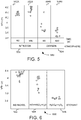
- FIG. 5 illustrates comparative chart 500, showing a comparison of threshold voltages of the semiconductor devices having the CMOS compatible contact layers fabricated by thermally treating the GaN based structure in different atmospheres and for different time durations.
- graph 502A and graph 502B illustrate the threshold voltages of the semiconductor devices having the CMOS compatible contact layers fabricated in the N 2 atmosphere for 60 seconds and 600 seconds, respectively.
- graph 504A and graph 504B illustrate the threshold voltages of the semiconductor devices having the CMOS compatible contact layers fabricated in the O 2 atmosphere for 60 seconds and 600 seconds, respectively.
- threshold voltage range in graph 502A and graph 502B is mainly between 4.25v to 4.45v and 4.4v to 4.6v, respectively.
- threshold voltage range in graph 504A and graph 504B is mainly between 3.625v to 3.7v and 3.4v to 3.45v, respectively. Therefore, it is observed that there is a significant reduction in the threshold voltages when the CMOS compatible contact layers fabricated in the O 2 atmosphere.
- FIG. 6 illustrates comparative chart 600, showing a comparison of threshold voltages of the semiconductor devices having the CMOS compatible contact layers fabricated by removing the Ni layer using different etchants, in accordance with the method described in FIG. 1 .
- graph 602 illustrates the threshold voltages of the semiconductor devices having the CMOS compatible contact layers fabricated without the Ni layer.
- graph 604 illustrates the threshold voltages of the semiconductor devices, when the Ni layer is etched for 10 minutes using HCl+HNO 3 +H 2 O having the ratio of 3:1:2.
- graph 606 illustrates the threshold voltages of the semiconductor devices, when the Ni layer is etched for 2 minutes using H 2 SO 4 +H 2 O 2 .
- threshold voltage range is 3.8v to 4.4v.
- the threshold voltages of the semiconductor devices are in the range of 3.2v to 4.1v.
- the threshold voltages of the semiconductor devices are in the range of 2.9v to 3v. Therefore, it is observed that there is a significant drop in the threshold voltages of the semiconductor devices when the Ni layer is etched using H 2 SO 4 +H 2 O 2 .
- the semiconductor devices having the CMOS compatible contact layers fabricated in accordance with the method described in FIG. 1 show better electrical characteristics as compared to the approaches used in the prior art. Further, by using the CMOS compatible contact layers there is a reduction in the cost of fabricating the semiconductor devices. In other words, by using the CMOS compatible contact layers, the economy-of-scale of existing CMOS production lines is effectively used during the fabrication of the semiconductor devices.
Claims (6)
- Procédé de fabrication d'une couche de contact compatible de semi-conducteur d'oxyde métallique complémentaire (CMOS) sur une couche de nitrure de gallium (GaN) de type p d'une structure à base de GaN, comprenant :- le revenu d'une structure à base de GaN à environ 750 °C dans une atmosphère d'azote avant de déposer une couche de nickel ;- le dépôt de la couche de nickel (Ni) sur la couche de GaN de type p ;- le traitement thermique de la structure à base de GaN dans une plage de températures de 350 °C à 500 °C lors du dépôt de la couche de Ni ;- le retrait de la couche de Ni en utilisant un agent de gravure lors du traitement thermique de la structure à base de GaN ; et- le dépôt de la couche de contact compatible de CMOS sur la couche de GaN de type p lors du retrait de la couche de Ni.
- Procédé selon la revendication 1, dans lequel la couche de GaN de type p comprend des dopants de magnésium (Mg).
- Procédé selon l'une quelconque des revendications précédentes, dans lequel le traitement thermique de la structure à base de GaN comprend en outre le traitement thermique de la structure à base de GaN dans une atmosphère d'oxygène pendant environ 60 secondes.
- Procédé selon l'une quelconque des revendications précédentes, dans lequel la couche de Ni présente une épaisseur de 5 nm à 15 nm.
- Procédé selon l'une quelconque des revendications précédentes, dans lequel l'agent de gravure comprend une solution d'acide sulfurique (H2SO4) et de peroxyde d'hydrogène (H2O2).
- Procédé selon l'une quelconque des revendications précédentes, dans lequel la couche de contact compatible de CMOS comprend une structure multicouche de titane, d'aluminium et de titane (TiAlTi).
Priority Applications (1)
| Application Number | Priority Date | Filing Date | Title |
|---|---|---|---|
| EP14189155.6A EP2881982B1 (fr) | 2013-12-05 | 2014-10-16 | Procédé de fabrication de couches de contact compatibles CMOS dans des dispositifs à semi-conducteurs |
Applications Claiming Priority (2)
| Application Number | Priority Date | Filing Date | Title |
|---|---|---|---|
| EP13195799 | 2013-12-05 | ||
| EP14189155.6A EP2881982B1 (fr) | 2013-12-05 | 2014-10-16 | Procédé de fabrication de couches de contact compatibles CMOS dans des dispositifs à semi-conducteurs |
Publications (3)
| Publication Number | Publication Date |
|---|---|
| EP2881982A2 EP2881982A2 (fr) | 2015-06-10 |
| EP2881982A3 EP2881982A3 (fr) | 2015-08-26 |
| EP2881982B1 true EP2881982B1 (fr) | 2019-09-04 |
Family
ID=49759051
Family Applications (1)
| Application Number | Title | Priority Date | Filing Date |
|---|---|---|---|
| EP14189155.6A Active EP2881982B1 (fr) | 2013-12-05 | 2014-10-16 | Procédé de fabrication de couches de contact compatibles CMOS dans des dispositifs à semi-conducteurs |
Country Status (3)
| Country | Link |
|---|---|
| US (2) | US20150162212A1 (fr) |
| EP (1) | EP2881982B1 (fr) |
| JP (1) | JP2015109438A (fr) |
Families Citing this family (2)
| Publication number | Priority date | Publication date | Assignee | Title |
|---|---|---|---|---|
| TWI568016B (zh) * | 2014-12-23 | 2017-01-21 | 錼創科技股份有限公司 | 半導體發光元件 |
| CN107180896B (zh) * | 2017-04-27 | 2019-06-28 | 华灿光电(浙江)有限公司 | 一种发光二极管的外延片及其制备方法 |
Citations (3)
| Publication number | Priority date | Publication date | Assignee | Title |
|---|---|---|---|---|
| JPH05183189A (ja) * | 1991-11-08 | 1993-07-23 | Nichia Chem Ind Ltd | p型窒化ガリウム系化合物半導体の製造方法。 |
| US20040000671A1 (en) * | 2002-06-28 | 2004-01-01 | Kopin Corporation | Electrode for p-type gallium nitride-based semiconductors |
| WO2013143289A1 (fr) * | 2012-03-28 | 2013-10-03 | 华为技术有限公司 | Substrat de gan, dispositif à semi-conducteur et procédé de fabrication de ceux-ci. |
Family Cites Families (58)
| Publication number | Priority date | Publication date | Assignee | Title |
|---|---|---|---|---|
| JPS63276267A (ja) * | 1987-05-08 | 1988-11-14 | Fujitsu Ltd | 半導体装置の製造方法 |
| JPH08250768A (ja) * | 1995-03-13 | 1996-09-27 | Toyoda Gosei Co Ltd | 半導体光素子 |
| WO1997008744A1 (fr) * | 1995-08-24 | 1997-03-06 | Sony Corporation | Lamine permettant de former une electrode ohmique et electrode ohmique |
| JP3292044B2 (ja) * | 1996-05-31 | 2002-06-17 | 豊田合成株式会社 | p伝導形3族窒化物半導体の電極パッド及びそれを有した素子及び素子の製造方法 |
| JP3289617B2 (ja) * | 1996-10-03 | 2002-06-10 | 豊田合成株式会社 | GaN系半導体素子の製造方法 |
| JPH1174559A (ja) * | 1997-08-28 | 1999-03-16 | Fuji Photo Film Co Ltd | 半導体発光素子および露光装置 |
| JP3509514B2 (ja) * | 1997-11-13 | 2004-03-22 | 豊田合成株式会社 | 窒化ガリウム系化合物半導体の製造方法 |
| JP4026294B2 (ja) * | 2000-03-07 | 2007-12-26 | 豊田合成株式会社 | Iii族窒化物系化合物半導体素子の製造方法 |
| US6326294B1 (en) * | 2000-04-27 | 2001-12-04 | Kwangju Institute Of Science And Technology | Method of fabricating an ohmic metal electrode for use in nitride compound semiconductor devices |
| JP4652530B2 (ja) * | 2000-07-10 | 2011-03-16 | 昭和電工株式会社 | 窒化ガリウム系化合物半導体発光素子の作製方法 |
| JP4148664B2 (ja) * | 2001-02-02 | 2008-09-10 | 三洋電機株式会社 | 窒化物系半導体レーザ素子およびその形成方法 |
| JP3520919B2 (ja) * | 2001-03-27 | 2004-04-19 | 士郎 酒井 | 窒化物系半導体装置の製造方法 |
| US7029939B2 (en) * | 2001-06-18 | 2006-04-18 | Toyoda Gosei Co., Ltd. | P-type semiconductor manufacturing method and semiconductor device |
| TW502438B (en) * | 2001-07-23 | 2002-09-11 | Uni Light Technology Inc | Semiconductor device with ohmic contact and method for producing the same |
| US6605832B2 (en) * | 2001-07-31 | 2003-08-12 | Xerox Corporation | Semiconductor structures having reduced contact resistance |
| JP4023121B2 (ja) * | 2001-09-06 | 2007-12-19 | 豊田合成株式会社 | n型電極、III族窒化物系化合物半導体素子、n型電極の製造方法、及びIII族窒化物系化合物半導体素子の製造方法 |
| KR100467316B1 (ko) * | 2002-03-20 | 2005-01-24 | 학교법인 포항공과대학교 | 갈륨나이트라이드계 광소자의 p형 오믹 전극 및 그 제조방법 |
| KR100491968B1 (ko) * | 2002-03-25 | 2005-05-27 | 학교법인 포항공과대학교 | 갈륨나이트라이드계 광소자의 p형 오믹 전극의 제조방법 |
| EP1892764B1 (fr) * | 2002-08-29 | 2016-03-09 | Seoul Semiconductor Co., Ltd. | Dispositif électroluminescent ayant des diodes électro-luminescentes |
| JP4311000B2 (ja) * | 2002-11-28 | 2009-08-12 | 日亜化学工業株式会社 | 窒化物半導体発光素子とその製造方法 |
| KR100612832B1 (ko) * | 2003-05-07 | 2006-08-18 | 삼성전자주식회사 | 고성능의 질화갈륨계 광소자 구현을 위한 니켈계 고용체를 이용한 오믹 접촉 형성을 위한 금속박막 및 그 제조방법 |
| KR100707167B1 (ko) * | 2003-07-11 | 2007-04-13 | 삼성전자주식회사 | 고성능의 질화갈륨계 광소자 구현을 위한 p형 열전산화물을 형성하는 2원계 및 3원계 합금 또는 고용체박막을 이용한 오믹접촉 형성을 위한 박막전극 및 그제조방법 |
| JP4030534B2 (ja) * | 2003-07-25 | 2008-01-09 | 昭和電工株式会社 | 化合物半導体発光素子およびその製造方法 |
| KR100506736B1 (ko) * | 2003-10-10 | 2005-08-08 | 삼성전기주식회사 | 질화갈륨계 반도체 발광 소자 및 그 제조방법 |
| KR100571819B1 (ko) * | 2003-10-16 | 2006-04-17 | 삼성전자주식회사 | 질화물계 발광소자 및 그 제조방법 |
| US7009215B2 (en) * | 2003-10-24 | 2006-03-07 | General Electric Company | Group III-nitride based resonant cavity light emitting devices fabricated on single crystal gallium nitride substrates |
| WO2005041283A1 (fr) * | 2003-10-27 | 2005-05-06 | Sumitomo Electric Industries, Ltd. | Substrat semi-conducteur de nitrure de gallium et procede de production correspondant |
| EP1697983B1 (fr) * | 2003-12-09 | 2012-06-13 | The Regents of The University of California | Diodes electroluminescentes a base de nitrure de gallium tres efficaces grace a une surface rendue rugueuse |
| KR100590532B1 (ko) * | 2003-12-22 | 2006-06-15 | 삼성전자주식회사 | 플립칩형 질화물계 발광소자 및 그 제조방법 |
| US20050167681A1 (en) * | 2004-02-04 | 2005-08-04 | Samsung Electronics Co., Ltd. | Electrode layer, light emitting device including the same, and method of forming the electrode layer |
| US7547928B2 (en) * | 2004-06-30 | 2009-06-16 | Interuniversitair Microelektronica Centrum (Imec) | AlGaN/GaN high electron mobility transistor devices |
| KR100773538B1 (ko) * | 2004-10-07 | 2007-11-07 | 삼성전자주식회사 | 반사 전극 및 이를 구비하는 화합물 반도체 발광소자 |
| JP4301136B2 (ja) * | 2004-10-18 | 2009-07-22 | サンケン電気株式会社 | 半導体発光素子およびその製造方法 |
| JP2006324628A (ja) * | 2005-05-16 | 2006-11-30 | Interuniv Micro Electronica Centrum Vzw | 完全ケイ化ゲート形成方法及び当該方法によって得られたデバイス |
| CN101138074A (zh) * | 2005-06-03 | 2008-03-05 | 古河电气工业株式会社 | Ⅲ-ⅴ族氮化物系化合物半导体装置及电极形成方法 |
| TWI255568B (en) * | 2005-09-15 | 2006-05-21 | Chipmos Technologies Inc | Light emitting diode and fabricating method thereof |
| JP4694395B2 (ja) * | 2006-03-22 | 2011-06-08 | 日本オプネクスト株式会社 | 窒化物半導体発光素子及びその製造方法 |
| WO2009012536A1 (fr) * | 2007-07-20 | 2009-01-29 | Interuniversitair Microelektronica Centrum | Contacts damasquinés sur des dispositifs cmos iii-v |
| JP2009212472A (ja) * | 2008-03-06 | 2009-09-17 | Rohm Co Ltd | 窒化物半導体素子 |
| JP2010232279A (ja) * | 2009-03-26 | 2010-10-14 | Furukawa Electric Co Ltd:The | 電界効果トランジスタ |
| KR101694883B1 (ko) * | 2009-04-08 | 2017-01-10 | 이피션트 파워 컨버젼 코퍼레이션 | 역확산 억제 구조 |
| JP2013514662A (ja) * | 2009-12-16 | 2013-04-25 | ナショナル セミコンダクター コーポレーション | ガリウム窒化物又は他の窒化物ベースのパワーデバイスのためのゲルマニウムを含む低オーミックコンタクト |
| KR101408610B1 (ko) * | 2009-12-21 | 2014-06-17 | 가부시끼가이샤 도시바 | 질화물 반도체 발광 소자 및 그 제조 방법 |
| US20110291147A1 (en) * | 2010-05-25 | 2011-12-01 | Yongjun Jeff Hu | Ohmic contacts for semiconductor structures |
| JP2012084739A (ja) * | 2010-10-13 | 2012-04-26 | Sumitomo Electric Ind Ltd | 半導体装置およびその製造方法 |
| US9070758B2 (en) * | 2011-06-20 | 2015-06-30 | Imec | CMOS compatible method for manufacturing a HEMT device and the HEMT device thereof |
| US9666764B2 (en) * | 2012-04-09 | 2017-05-30 | Cree, Inc. | Wafer level packaging of multiple light emitting diodes (LEDs) on a single carrier die |
| JP5713856B2 (ja) * | 2011-09-26 | 2015-05-07 | 株式会社東芝 | 光透過型金属電極、電子装置及び光学素子 |
| US9281439B2 (en) * | 2011-09-30 | 2016-03-08 | Soko Kagaku Co., Ltd. | Nitride semiconductor element and method for producing same |
| US9111904B2 (en) * | 2011-11-29 | 2015-08-18 | Taiwan Semiconductor Manufacturing Company, Ltd. | Substrate breakdown voltage improvement for group III-nitride on a silicon substrate |
| EP2791983A4 (fr) * | 2011-12-12 | 2015-08-12 | Sensor Electronic Tech Inc | Contact réfléchissant les ultraviolets |
| KR20130127209A (ko) * | 2012-05-14 | 2013-11-22 | 삼성전자주식회사 | 질화갈륨계 반도체 발광소자의 제조방법 |
| JP6052962B2 (ja) * | 2012-08-03 | 2016-12-27 | スタンレー電気株式会社 | 半導体発光装置 |
| CN102789976A (zh) * | 2012-08-28 | 2012-11-21 | 厦门市三安光电科技有限公司 | 一种GaN基LED芯片的制作方法 |
| EP2806463A1 (fr) * | 2013-05-22 | 2014-11-26 | Imec | Contacts ohmiques à basse température pour dispositifs de puissance III-N |
| US9245991B2 (en) * | 2013-08-12 | 2016-01-26 | Taiwan Semiconductor Manufacturing Company, Ltd. | Semiconductor device, high electron mobility transistor (HEMT) and method of manufacturing |
| EP2843708A1 (fr) * | 2013-08-28 | 2015-03-04 | Seoul Semiconductor Co., Ltd. | Transistors à base de nitrure et procédés de fabrication de celui-ci |
| US20150279961A1 (en) * | 2014-03-31 | 2015-10-01 | National Tsing Hua University | METHOD OF MANUFACTURING HIGH POWER VERTICAL GaN-PIN DIODE |
-
2014
- 2014-10-16 EP EP14189155.6A patent/EP2881982B1/fr active Active
- 2014-10-28 JP JP2014219046A patent/JP2015109438A/ja active Pending
- 2014-11-24 US US14/551,398 patent/US20150162212A1/en not_active Abandoned
-
2016
- 2016-01-06 US US14/989,114 patent/US9698309B2/en active Active
Patent Citations (4)
| Publication number | Priority date | Publication date | Assignee | Title |
|---|---|---|---|---|
| JPH05183189A (ja) * | 1991-11-08 | 1993-07-23 | Nichia Chem Ind Ltd | p型窒化ガリウム系化合物半導体の製造方法。 |
| US20040000671A1 (en) * | 2002-06-28 | 2004-01-01 | Kopin Corporation | Electrode for p-type gallium nitride-based semiconductors |
| WO2013143289A1 (fr) * | 2012-03-28 | 2013-10-03 | 华为技术有限公司 | Substrat de gan, dispositif à semi-conducteur et procédé de fabrication de ceux-ci. |
| EP2806459A1 (fr) * | 2012-03-28 | 2014-11-26 | Huawei Technologies Co., Ltd | Substrat de gan, dispositif à semi-conducteur et procédé de fabrication de ceux-ci. |
Also Published As
| Publication number | Publication date |
|---|---|
| US9698309B2 (en) | 2017-07-04 |
| US20150162212A1 (en) | 2015-06-11 |
| JP2015109438A (ja) | 2015-06-11 |
| EP2881982A3 (fr) | 2015-08-26 |
| EP2881982A2 (fr) | 2015-06-10 |
| US20160118542A1 (en) | 2016-04-28 |
Similar Documents
| Publication | Publication Date | Title |
|---|---|---|
| KR100867518B1 (ko) | 질화물계 반도체 발광소자의 제조방법 | |
| US7875534B2 (en) | Realizing N-face III-nitride semiconductors by nitridation treatment | |
| KR100755656B1 (ko) | 질화물계 반도체 발광소자의 제조방법 | |
| JP5103979B2 (ja) | III族窒化物系化合物半導体に対する電極形成方法及びp型III族窒化物系化合物半導体の製造方法 | |
| JP2008244307A (ja) | 半導体発光素子および窒化物半導体発光素子 | |
| WO2012137781A1 (fr) | Corps semi-conducteur empilé et son procédé de fabrication, et élément semi-conducteur | |
| KR100988194B1 (ko) | 반도체 발광 소자 및 그 제조 방법 | |
| EP2881982B1 (fr) | Procédé de fabrication de couches de contact compatibles CMOS dans des dispositifs à semi-conducteurs | |
| US8431936B2 (en) | Method for fabricating a p-type semiconductor structure | |
| EP2693499B1 (fr) | Dispositif électroluminescent semi-conducteur et son procédé de fabrication | |
| JP2009272441A (ja) | 半導体装置および半導体装置の製造方法 | |
| TWI727116B (zh) | 半導體發光元件的製造方法 | |
| CN112750925B (zh) | 深紫外led器件结构及其制备方法 | |
| WO2011086730A1 (fr) | Élément à semi-conducteur nitrure d'élément du groupe iii | |
| TWI736707B (zh) | 半導體發光元件的製造方法 | |
| JP2010245109A (ja) | Iii族窒化物系半導体素子、及び電極を作製する方法 | |
| US20220140198A1 (en) | Light Emitting Diode Devices | |
| JP2006066892A (ja) | 発光素子およびその製造方法 | |
| CN111316453A (zh) | 半导体发光元件及半导体发光元件的制造方法 | |
| JP6260159B2 (ja) | 窒化物半導体発光ダイオード、及びその製造方法 | |
| KR101045949B1 (ko) | 질화물 반도체 발광소자 및 이의 제조 방법 | |
| Kim et al. | Highly efficient InGaN/GaN blue LED grown on Si (111) substrate | |
| CN104900767A (zh) | 发光二极管p型掺杂层生长方法 | |
| KR20140012584A (ko) | 질화물계 반도체 소자 | |
| US8420424B2 (en) | Method for manufacturing semiconductor light emmiting device |
Legal Events
| Date | Code | Title | Description |
|---|---|---|---|
| PUAI | Public reference made under article 153(3) epc to a published international application that has entered the european phase |
Free format text: ORIGINAL CODE: 0009012 |
|
| 17P | Request for examination filed |
Effective date: 20141016 |
|
| AK | Designated contracting states |
Kind code of ref document: A2 Designated state(s): AL AT BE BG CH CY CZ DE DK EE ES FI FR GB GR HR HU IE IS IT LI LT LU LV MC MK MT NL NO PL PT RO RS SE SI SK SM TR |
|
| AX | Request for extension of the european patent |
Extension state: BA ME |
|
| PUAL | Search report despatched |
Free format text: ORIGINAL CODE: 0009013 |
|
| RIC1 | Information provided on ipc code assigned before grant |
Ipc: H01L 21/3205 20060101ALI20150709BHEP Ipc: H01L 21/8252 20060101AFI20150709BHEP Ipc: H01L 21/3213 20060101ALI20150709BHEP Ipc: H01L 29/45 20060101ALI20150709BHEP |
|
| AK | Designated contracting states |
Kind code of ref document: A3 Designated state(s): AL AT BE BG CH CY CZ DE DK EE ES FI FR GB GR HR HU IE IS IT LI LT LU LV MC MK MT NL NO PL PT RO RS SE SI SK SM TR |
|
| AX | Request for extension of the european patent |
Extension state: BA ME |
|
| RIC1 | Information provided on ipc code assigned before grant |
Ipc: H01L 21/3205 20060101ALI20150717BHEP Ipc: H01L 29/45 20060101ALI20150717BHEP Ipc: H01L 21/8252 20060101AFI20150717BHEP Ipc: H01L 21/3213 20060101ALI20150717BHEP |
|
| R17P | Request for examination filed (corrected) |
Effective date: 20160210 |
|
| RBV | Designated contracting states (corrected) |
Designated state(s): AL AT BE BG CH CY CZ DE DK EE ES FI FR GB GR HR HU IE IS IT LI LT LU LV MC MK MT NL NO PL PT RO RS SE SI SK SM TR |
|
| STAA | Information on the status of an ep patent application or granted ep patent |
Free format text: STATUS: EXAMINATION IS IN PROGRESS |
|
| 17Q | First examination report despatched |
Effective date: 20170425 |
|
| GRAP | Despatch of communication of intention to grant a patent |
Free format text: ORIGINAL CODE: EPIDOSNIGR1 |
|
| STAA | Information on the status of an ep patent application or granted ep patent |
Free format text: STATUS: GRANT OF PATENT IS INTENDED |
|
| RIC1 | Information provided on ipc code assigned before grant |
Ipc: H01L 21/3205 20060101ALI20181102BHEP Ipc: H01L 29/207 20060101ALI20181102BHEP Ipc: H01L 33/40 20100101ALI20181102BHEP Ipc: H01L 29/45 20060101ALI20181102BHEP Ipc: H01L 29/20 20060101ALI20181102BHEP Ipc: H01L 21/324 20060101ALI20181102BHEP Ipc: H01L 21/3213 20060101ALI20181102BHEP Ipc: H01L 33/32 20100101ALI20181102BHEP Ipc: H01L 21/8252 20060101AFI20181102BHEP |
|
| INTG | Intention to grant announced |
Effective date: 20181203 |
|
| GRAJ | Information related to disapproval of communication of intention to grant by the applicant or resumption of examination proceedings by the epo deleted |
Free format text: ORIGINAL CODE: EPIDOSDIGR1 |
|
| STAA | Information on the status of an ep patent application or granted ep patent |
Free format text: STATUS: EXAMINATION IS IN PROGRESS |
|
| GRAP | Despatch of communication of intention to grant a patent |
Free format text: ORIGINAL CODE: EPIDOSNIGR1 |
|
| STAA | Information on the status of an ep patent application or granted ep patent |
Free format text: STATUS: GRANT OF PATENT IS INTENDED |
|
| INTC | Intention to grant announced (deleted) | ||
| INTG | Intention to grant announced |
Effective date: 20190508 |
|
| GRAS | Grant fee paid |
Free format text: ORIGINAL CODE: EPIDOSNIGR3 |
|
| GRAA | (expected) grant |
Free format text: ORIGINAL CODE: 0009210 |
|
| STAA | Information on the status of an ep patent application or granted ep patent |
Free format text: STATUS: THE PATENT HAS BEEN GRANTED |
|
| AK | Designated contracting states |
Kind code of ref document: B1 Designated state(s): AL AT BE BG CH CY CZ DE DK EE ES FI FR GB GR HR HU IE IS IT LI LT LU LV MC MK MT NL NO PL PT RO RS SE SI SK SM TR |
|
| REG | Reference to a national code |
Ref country code: GB Ref legal event code: FG4D |
|
| REG | Reference to a national code |
Ref country code: CH Ref legal event code: EP |
|
| REG | Reference to a national code |
Ref country code: AT Ref legal event code: REF Ref document number: 1176568 Country of ref document: AT Kind code of ref document: T Effective date: 20190915 |
|
| REG | Reference to a national code |
Ref country code: DE Ref legal event code: R096 Ref document number: 602014052875 Country of ref document: DE |
|
| REG | Reference to a national code |
Ref country code: IE Ref legal event code: FG4D |
|
| REG | Reference to a national code |
Ref country code: NL Ref legal event code: MP Effective date: 20190904 |
|
| REG | Reference to a national code |
Ref country code: LT Ref legal event code: MG4D |
|
| PG25 | Lapsed in a contracting state [announced via postgrant information from national office to epo] |
Ref country code: SE Free format text: LAPSE BECAUSE OF FAILURE TO SUBMIT A TRANSLATION OF THE DESCRIPTION OR TO PAY THE FEE WITHIN THE PRESCRIBED TIME-LIMIT Effective date: 20190904 Ref country code: BG Free format text: LAPSE BECAUSE OF FAILURE TO SUBMIT A TRANSLATION OF THE DESCRIPTION OR TO PAY THE FEE WITHIN THE PRESCRIBED TIME-LIMIT Effective date: 20191204 Ref country code: NO Free format text: LAPSE BECAUSE OF FAILURE TO SUBMIT A TRANSLATION OF THE DESCRIPTION OR TO PAY THE FEE WITHIN THE PRESCRIBED TIME-LIMIT Effective date: 20191204 Ref country code: FI Free format text: LAPSE BECAUSE OF FAILURE TO SUBMIT A TRANSLATION OF THE DESCRIPTION OR TO PAY THE FEE WITHIN THE PRESCRIBED TIME-LIMIT Effective date: 20190904 Ref country code: HR Free format text: LAPSE BECAUSE OF FAILURE TO SUBMIT A TRANSLATION OF THE DESCRIPTION OR TO PAY THE FEE WITHIN THE PRESCRIBED TIME-LIMIT Effective date: 20190904 Ref country code: LT Free format text: LAPSE BECAUSE OF FAILURE TO SUBMIT A TRANSLATION OF THE DESCRIPTION OR TO PAY THE FEE WITHIN THE PRESCRIBED TIME-LIMIT Effective date: 20190904 |
|
| PG25 | Lapsed in a contracting state [announced via postgrant information from national office to epo] |
Ref country code: AL Free format text: LAPSE BECAUSE OF FAILURE TO SUBMIT A TRANSLATION OF THE DESCRIPTION OR TO PAY THE FEE WITHIN THE PRESCRIBED TIME-LIMIT Effective date: 20190904 Ref country code: ES Free format text: LAPSE BECAUSE OF FAILURE TO SUBMIT A TRANSLATION OF THE DESCRIPTION OR TO PAY THE FEE WITHIN THE PRESCRIBED TIME-LIMIT Effective date: 20190904 Ref country code: GR Free format text: LAPSE BECAUSE OF FAILURE TO SUBMIT A TRANSLATION OF THE DESCRIPTION OR TO PAY THE FEE WITHIN THE PRESCRIBED TIME-LIMIT Effective date: 20191205 Ref country code: RS Free format text: LAPSE BECAUSE OF FAILURE TO SUBMIT A TRANSLATION OF THE DESCRIPTION OR TO PAY THE FEE WITHIN THE PRESCRIBED TIME-LIMIT Effective date: 20190904 Ref country code: LV Free format text: LAPSE BECAUSE OF FAILURE TO SUBMIT A TRANSLATION OF THE DESCRIPTION OR TO PAY THE FEE WITHIN THE PRESCRIBED TIME-LIMIT Effective date: 20190904 |
|
| REG | Reference to a national code |
Ref country code: AT Ref legal event code: MK05 Ref document number: 1176568 Country of ref document: AT Kind code of ref document: T Effective date: 20190904 |
|
| PG25 | Lapsed in a contracting state [announced via postgrant information from national office to epo] |
Ref country code: PT Free format text: LAPSE BECAUSE OF FAILURE TO SUBMIT A TRANSLATION OF THE DESCRIPTION OR TO PAY THE FEE WITHIN THE PRESCRIBED TIME-LIMIT Effective date: 20200106 Ref country code: PL Free format text: LAPSE BECAUSE OF FAILURE TO SUBMIT A TRANSLATION OF THE DESCRIPTION OR TO PAY THE FEE WITHIN THE PRESCRIBED TIME-LIMIT Effective date: 20190904 Ref country code: EE Free format text: LAPSE BECAUSE OF FAILURE TO SUBMIT A TRANSLATION OF THE DESCRIPTION OR TO PAY THE FEE WITHIN THE PRESCRIBED TIME-LIMIT Effective date: 20190904 Ref country code: RO Free format text: LAPSE BECAUSE OF FAILURE TO SUBMIT A TRANSLATION OF THE DESCRIPTION OR TO PAY THE FEE WITHIN THE PRESCRIBED TIME-LIMIT Effective date: 20190904 Ref country code: IT Free format text: LAPSE BECAUSE OF FAILURE TO SUBMIT A TRANSLATION OF THE DESCRIPTION OR TO PAY THE FEE WITHIN THE PRESCRIBED TIME-LIMIT Effective date: 20190904 Ref country code: NL Free format text: LAPSE BECAUSE OF FAILURE TO SUBMIT A TRANSLATION OF THE DESCRIPTION OR TO PAY THE FEE WITHIN THE PRESCRIBED TIME-LIMIT Effective date: 20190904 Ref country code: AT Free format text: LAPSE BECAUSE OF FAILURE TO SUBMIT A TRANSLATION OF THE DESCRIPTION OR TO PAY THE FEE WITHIN THE PRESCRIBED TIME-LIMIT Effective date: 20190904 |
|
| PG25 | Lapsed in a contracting state [announced via postgrant information from national office to epo] |
Ref country code: IS Free format text: LAPSE BECAUSE OF FAILURE TO SUBMIT A TRANSLATION OF THE DESCRIPTION OR TO PAY THE FEE WITHIN THE PRESCRIBED TIME-LIMIT Effective date: 20200224 Ref country code: CZ Free format text: LAPSE BECAUSE OF FAILURE TO SUBMIT A TRANSLATION OF THE DESCRIPTION OR TO PAY THE FEE WITHIN THE PRESCRIBED TIME-LIMIT Effective date: 20190904 Ref country code: SK Free format text: LAPSE BECAUSE OF FAILURE TO SUBMIT A TRANSLATION OF THE DESCRIPTION OR TO PAY THE FEE WITHIN THE PRESCRIBED TIME-LIMIT Effective date: 20190904 Ref country code: SM Free format text: LAPSE BECAUSE OF FAILURE TO SUBMIT A TRANSLATION OF THE DESCRIPTION OR TO PAY THE FEE WITHIN THE PRESCRIBED TIME-LIMIT Effective date: 20190904 |
|
| REG | Reference to a national code |
Ref country code: CH Ref legal event code: PL |
|
| REG | Reference to a national code |
Ref country code: DE Ref legal event code: R097 Ref document number: 602014052875 Country of ref document: DE |
|
| PLBE | No opposition filed within time limit |
Free format text: ORIGINAL CODE: 0009261 |
|
| STAA | Information on the status of an ep patent application or granted ep patent |
Free format text: STATUS: NO OPPOSITION FILED WITHIN TIME LIMIT |
|
| PG2D | Information on lapse in contracting state deleted |
Ref country code: IS |
|
| PG25 | Lapsed in a contracting state [announced via postgrant information from national office to epo] |
Ref country code: LI Free format text: LAPSE BECAUSE OF NON-PAYMENT OF DUE FEES Effective date: 20191031 Ref country code: DK Free format text: LAPSE BECAUSE OF FAILURE TO SUBMIT A TRANSLATION OF THE DESCRIPTION OR TO PAY THE FEE WITHIN THE PRESCRIBED TIME-LIMIT Effective date: 20190904 Ref country code: LU Free format text: LAPSE BECAUSE OF NON-PAYMENT OF DUE FEES Effective date: 20191016 Ref country code: CH Free format text: LAPSE BECAUSE OF NON-PAYMENT OF DUE FEES Effective date: 20191031 Ref country code: IS Free format text: LAPSE BECAUSE OF FAILURE TO SUBMIT A TRANSLATION OF THE DESCRIPTION OR TO PAY THE FEE WITHIN THE PRESCRIBED TIME-LIMIT Effective date: 20200105 |
|
| 26N | No opposition filed |
Effective date: 20200605 |
|
| REG | Reference to a national code |
Ref country code: BE Ref legal event code: MM Effective date: 20191031 |
|
| PG25 | Lapsed in a contracting state [announced via postgrant information from national office to epo] |
Ref country code: BE Free format text: LAPSE BECAUSE OF NON-PAYMENT OF DUE FEES Effective date: 20191031 Ref country code: SI Free format text: LAPSE BECAUSE OF FAILURE TO SUBMIT A TRANSLATION OF THE DESCRIPTION OR TO PAY THE FEE WITHIN THE PRESCRIBED TIME-LIMIT Effective date: 20190904 Ref country code: MC Free format text: LAPSE BECAUSE OF FAILURE TO SUBMIT A TRANSLATION OF THE DESCRIPTION OR TO PAY THE FEE WITHIN THE PRESCRIBED TIME-LIMIT Effective date: 20190904 |
|
| GBPC | Gb: european patent ceased through non-payment of renewal fee |
Effective date: 20191204 |
|
| PG25 | Lapsed in a contracting state [announced via postgrant information from national office to epo] |
Ref country code: GB Free format text: LAPSE BECAUSE OF NON-PAYMENT OF DUE FEES Effective date: 20191204 Ref country code: IE Free format text: LAPSE BECAUSE OF NON-PAYMENT OF DUE FEES Effective date: 20191016 |
|
| PG25 | Lapsed in a contracting state [announced via postgrant information from national office to epo] |
Ref country code: CY Free format text: LAPSE BECAUSE OF FAILURE TO SUBMIT A TRANSLATION OF THE DESCRIPTION OR TO PAY THE FEE WITHIN THE PRESCRIBED TIME-LIMIT Effective date: 20190904 |
|
| PG25 | Lapsed in a contracting state [announced via postgrant information from national office to epo] |
Ref country code: MT Free format text: LAPSE BECAUSE OF FAILURE TO SUBMIT A TRANSLATION OF THE DESCRIPTION OR TO PAY THE FEE WITHIN THE PRESCRIBED TIME-LIMIT Effective date: 20190904 Ref country code: HU Free format text: LAPSE BECAUSE OF FAILURE TO SUBMIT A TRANSLATION OF THE DESCRIPTION OR TO PAY THE FEE WITHIN THE PRESCRIBED TIME-LIMIT; INVALID AB INITIO Effective date: 20141016 |
|
| PG25 | Lapsed in a contracting state [announced via postgrant information from national office to epo] |
Ref country code: TR Free format text: LAPSE BECAUSE OF FAILURE TO SUBMIT A TRANSLATION OF THE DESCRIPTION OR TO PAY THE FEE WITHIN THE PRESCRIBED TIME-LIMIT Effective date: 20190904 |
|
| PG25 | Lapsed in a contracting state [announced via postgrant information from national office to epo] |
Ref country code: MK Free format text: LAPSE BECAUSE OF FAILURE TO SUBMIT A TRANSLATION OF THE DESCRIPTION OR TO PAY THE FEE WITHIN THE PRESCRIBED TIME-LIMIT Effective date: 20190904 |
|
| P01 | Opt-out of the competence of the unified patent court (upc) registered |
Effective date: 20230513 |
|
| PGFP | Annual fee paid to national office [announced via postgrant information from national office to epo] |
Ref country code: FR Payment date: 20230920 Year of fee payment: 10 |
|
| PGFP | Annual fee paid to national office [announced via postgrant information from national office to epo] |
Ref country code: DE Payment date: 20230920 Year of fee payment: 10 |