EP2833391A1 - Halbleiterlaminat und verfahren zur herstellung davon, verfahren zur herstellung eines halbleiterbauelements, halbleiterbauelement, dotierungszusammensetzung, dotierungsinjektionsschicht und verfahren zur formung einer dotierten schicht - Google Patents
Halbleiterlaminat und verfahren zur herstellung davon, verfahren zur herstellung eines halbleiterbauelements, halbleiterbauelement, dotierungszusammensetzung, dotierungsinjektionsschicht und verfahren zur formung einer dotierten schicht Download PDFInfo
- Publication number
- EP2833391A1 EP2833391A1 EP13768368.6A EP13768368A EP2833391A1 EP 2833391 A1 EP2833391 A1 EP 2833391A1 EP 13768368 A EP13768368 A EP 13768368A EP 2833391 A1 EP2833391 A1 EP 2833391A1
- Authority
- EP
- European Patent Office
- Prior art keywords
- layer
- dopant
- light
- substrate
- semiconductor
- Prior art date
- Legal status (The legal status is an assumption and is not a legal conclusion. Google has not performed a legal analysis and makes no representation as to the accuracy of the status listed.)
- Withdrawn
Links
- 239000004065 semiconductor Substances 0.000 title claims abstract description 271
- 238000000034 method Methods 0.000 title claims abstract description 183
- 238000004519 manufacturing process Methods 0.000 title claims abstract description 53
- 239000002019 doping agent Substances 0.000 title claims description 458
- 238000002347 injection Methods 0.000 title claims description 219
- 239000007924 injection Substances 0.000 title claims description 219
- 239000000203 mixture Substances 0.000 title claims description 60
- 239000000758 substrate Substances 0.000 claims abstract description 301
- 239000011856 silicon-based particle Substances 0.000 claims abstract description 269
- 239000006185 dispersion Substances 0.000 claims abstract description 138
- XUIMIQQOPSSXEZ-UHFFFAOYSA-N Silicon Chemical compound [Si] XUIMIQQOPSSXEZ-UHFFFAOYSA-N 0.000 claims abstract description 56
- 229910052710 silicon Inorganic materials 0.000 claims abstract description 56
- 239000010703 silicon Substances 0.000 claims abstract description 56
- 238000001035 drying Methods 0.000 claims abstract description 48
- 230000001678 irradiating effect Effects 0.000 claims abstract description 26
- 239000002612 dispersion medium Substances 0.000 claims abstract description 24
- 239000011248 coating agent Substances 0.000 claims abstract description 16
- 238000000576 coating method Methods 0.000 claims abstract description 16
- 239000002245 particle Substances 0.000 claims description 198
- 238000002161 passivation Methods 0.000 claims description 150
- 150000001875 compounds Chemical class 0.000 claims description 59
- 239000000463 material Substances 0.000 claims description 40
- 239000012298 atmosphere Substances 0.000 claims description 32
- 239000010408 film Substances 0.000 claims description 28
- 239000011164 primary particle Substances 0.000 claims description 26
- 238000010521 absorption reaction Methods 0.000 claims description 25
- GNPVGFCGXDBREM-UHFFFAOYSA-N germanium atom Chemical compound [Ge] GNPVGFCGXDBREM-UHFFFAOYSA-N 0.000 claims description 16
- 239000011521 glass Substances 0.000 claims description 16
- 229910052732 germanium Inorganic materials 0.000 claims description 15
- VYPSYNLAJGMNEJ-UHFFFAOYSA-N Silicium dioxide Chemical compound O=[Si]=O VYPSYNLAJGMNEJ-UHFFFAOYSA-N 0.000 claims description 14
- 238000000151 deposition Methods 0.000 claims description 14
- 230000008569 process Effects 0.000 claims description 13
- 229910052814 silicon oxide Inorganic materials 0.000 claims description 12
- 239000002904 solvent Substances 0.000 claims description 12
- 230000001590 oxidative effect Effects 0.000 claims description 8
- 230000000717 retained effect Effects 0.000 claims description 8
- 150000003377 silicon compounds Chemical class 0.000 claims description 7
- 239000010409 thin film Substances 0.000 claims description 7
- 238000007639 printing Methods 0.000 claims description 6
- 239000007791 liquid phase Substances 0.000 claims description 4
- 150000002484 inorganic compounds Chemical class 0.000 claims description 3
- 229910010272 inorganic material Inorganic materials 0.000 claims description 3
- 150000002894 organic compounds Chemical class 0.000 claims description 3
- 229910004541 SiN Inorganic materials 0.000 claims 1
- PNEYBMLMFCGWSK-UHFFFAOYSA-N aluminium oxide Inorganic materials [O-2].[O-2].[O-2].[Al+3].[Al+3] PNEYBMLMFCGWSK-UHFFFAOYSA-N 0.000 claims 1
- 229910052681 coesite Inorganic materials 0.000 claims 1
- 229910052593 corundum Inorganic materials 0.000 claims 1
- 229910052906 cristobalite Inorganic materials 0.000 claims 1
- 239000000377 silicon dioxide Substances 0.000 claims 1
- 229910052682 stishovite Inorganic materials 0.000 claims 1
- 229910052905 tridymite Inorganic materials 0.000 claims 1
- 229910001845 yogo sapphire Inorganic materials 0.000 claims 1
- 239000010410 layer Substances 0.000 description 802
- KFZMGEQAYNKOFK-UHFFFAOYSA-N Isopropanol Chemical compound CC(C)O KFZMGEQAYNKOFK-UHFFFAOYSA-N 0.000 description 45
- 230000000052 comparative effect Effects 0.000 description 26
- 238000009792 diffusion process Methods 0.000 description 21
- 229910052581 Si3N4 Inorganic materials 0.000 description 20
- 125000004429 atom Chemical group 0.000 description 20
- 230000015572 biosynthetic process Effects 0.000 description 20
- 238000011156 evaluation Methods 0.000 description 20
- HQVNEWCFYHHQES-UHFFFAOYSA-N silicon nitride Chemical compound N12[Si]34N5[Si]62N3[Si]51N64 HQVNEWCFYHHQES-UHFFFAOYSA-N 0.000 description 20
- 238000000005 dynamic secondary ion mass spectrometry Methods 0.000 description 19
- 238000002360 preparation method Methods 0.000 description 18
- 239000000243 solution Substances 0.000 description 18
- 238000000445 field-emission scanning electron microscopy Methods 0.000 description 15
- 239000007789 gas Substances 0.000 description 15
- 239000007787 solid Substances 0.000 description 12
- 230000000694 effects Effects 0.000 description 11
- 238000001725 laser pyrolysis Methods 0.000 description 11
- IJGRMHOSHXDMSA-UHFFFAOYSA-N Atomic nitrogen Chemical compound N#N IJGRMHOSHXDMSA-UHFFFAOYSA-N 0.000 description 10
- CURLTUGMZLYLDI-UHFFFAOYSA-N Carbon dioxide Chemical compound O=C=O CURLTUGMZLYLDI-UHFFFAOYSA-N 0.000 description 10
- 238000005259 measurement Methods 0.000 description 10
- DNIAPMSPPWPWGF-UHFFFAOYSA-N Propylene glycol Chemical compound CC(O)CO DNIAPMSPPWPWGF-UHFFFAOYSA-N 0.000 description 9
- 238000010438 heat treatment Methods 0.000 description 9
- 238000004626 scanning electron microscopy Methods 0.000 description 9
- 238000005245 sintering Methods 0.000 description 9
- 238000002834 transmittance Methods 0.000 description 9
- 229910021417 amorphous silicon Inorganic materials 0.000 description 8
- 239000001569 carbon dioxide Substances 0.000 description 8
- 229910002092 carbon dioxide Inorganic materials 0.000 description 8
- 239000001257 hydrogen Substances 0.000 description 8
- 229910052739 hydrogen Inorganic materials 0.000 description 8
- BLRPTPMANUNPDV-UHFFFAOYSA-N Silane Chemical compound [SiH4] BLRPTPMANUNPDV-UHFFFAOYSA-N 0.000 description 7
- 238000002425 crystallisation Methods 0.000 description 7
- 230000008025 crystallization Effects 0.000 description 7
- 230000001771 impaired effect Effects 0.000 description 7
- CSCPPACGZOOCGX-UHFFFAOYSA-N Acetone Chemical compound CC(C)=O CSCPPACGZOOCGX-UHFFFAOYSA-N 0.000 description 6
- 238000007650 screen-printing Methods 0.000 description 6
- SCPYDCQAZCOKTP-UHFFFAOYSA-N silanol Chemical compound [SiH3]O SCPYDCQAZCOKTP-UHFFFAOYSA-N 0.000 description 6
- 238000004528 spin coating Methods 0.000 description 6
- LYCAIKOWRPUZTN-UHFFFAOYSA-N Ethylene glycol Chemical compound OCCO LYCAIKOWRPUZTN-UHFFFAOYSA-N 0.000 description 5
- 230000006866 deterioration Effects 0.000 description 5
- 238000012545 processing Methods 0.000 description 5
- XKRFYHLGVUSROY-UHFFFAOYSA-N Argon Chemical compound [Ar] XKRFYHLGVUSROY-UHFFFAOYSA-N 0.000 description 4
- ZOXJGFHDIHLPTG-UHFFFAOYSA-N Boron Chemical compound [B] ZOXJGFHDIHLPTG-UHFFFAOYSA-N 0.000 description 4
- GYHNNYVSQQEPJS-UHFFFAOYSA-N Gallium Chemical compound [Ga] GYHNNYVSQQEPJS-UHFFFAOYSA-N 0.000 description 4
- UFHFLCQGNIYNRP-UHFFFAOYSA-N Hydrogen Chemical compound [H][H] UFHFLCQGNIYNRP-UHFFFAOYSA-N 0.000 description 4
- SECXISVLQFMRJM-UHFFFAOYSA-N N-Methylpyrrolidone Chemical compound CN1CCCC1=O SECXISVLQFMRJM-UHFFFAOYSA-N 0.000 description 4
- 241000566150 Pandion haliaetus Species 0.000 description 4
- OAICVXFJPJFONN-UHFFFAOYSA-N Phosphorus Chemical compound [P] OAICVXFJPJFONN-UHFFFAOYSA-N 0.000 description 4
- 238000001069 Raman spectroscopy Methods 0.000 description 4
- 229910052796 boron Inorganic materials 0.000 description 4
- 238000007796 conventional method Methods 0.000 description 4
- 229910052733 gallium Inorganic materials 0.000 description 4
- 150000002431 hydrogen Chemical class 0.000 description 4
- 238000007641 inkjet printing Methods 0.000 description 4
- 229910052751 metal Inorganic materials 0.000 description 4
- 239000002184 metal Substances 0.000 description 4
- 238000012986 modification Methods 0.000 description 4
- 230000004048 modification Effects 0.000 description 4
- TWNQGVIAIRXVLR-UHFFFAOYSA-N oxo(oxoalumanyloxy)alumane Chemical compound O=[Al]O[Al]=O TWNQGVIAIRXVLR-UHFFFAOYSA-N 0.000 description 4
- 229910052698 phosphorus Inorganic materials 0.000 description 4
- 239000011574 phosphorus Substances 0.000 description 4
- XHXFXVLFKHQFAL-UHFFFAOYSA-N phosphoryl trichloride Chemical compound ClP(Cl)(Cl)=O XHXFXVLFKHQFAL-UHFFFAOYSA-N 0.000 description 4
- 238000004904 shortening Methods 0.000 description 4
- 238000004611 spectroscopical analysis Methods 0.000 description 4
- IUVCFHHAEHNCFT-INIZCTEOSA-N 2-[(1s)-1-[4-amino-3-(3-fluoro-4-propan-2-yloxyphenyl)pyrazolo[3,4-d]pyrimidin-1-yl]ethyl]-6-fluoro-3-(3-fluorophenyl)chromen-4-one Chemical compound C1=C(F)C(OC(C)C)=CC=C1C(C1=C(N)N=CN=C11)=NN1[C@@H](C)C1=C(C=2C=C(F)C=CC=2)C(=O)C2=CC(F)=CC=C2O1 IUVCFHHAEHNCFT-INIZCTEOSA-N 0.000 description 3
- OKTJSMMVPCPJKN-UHFFFAOYSA-N Carbon Chemical compound [C] OKTJSMMVPCPJKN-UHFFFAOYSA-N 0.000 description 3
- LFQSCWFLJHTTHZ-UHFFFAOYSA-N Ethanol Chemical compound CCO LFQSCWFLJHTTHZ-UHFFFAOYSA-N 0.000 description 3
- 238000004458 analytical method Methods 0.000 description 3
- 229910052799 carbon Inorganic materials 0.000 description 3
- 238000005229 chemical vapour deposition Methods 0.000 description 3
- 230000001419 dependent effect Effects 0.000 description 3
- SWXVUIWOUIDPGS-UHFFFAOYSA-N diacetone alcohol Natural products CC(=O)CC(C)(C)O SWXVUIWOUIDPGS-UHFFFAOYSA-N 0.000 description 3
- 238000002474 experimental method Methods 0.000 description 3
- 239000012535 impurity Substances 0.000 description 3
- 229910052757 nitrogen Inorganic materials 0.000 description 3
- 239000003960 organic solvent Substances 0.000 description 3
- 150000003961 organosilicon compounds Chemical class 0.000 description 3
- 230000003647 oxidation Effects 0.000 description 3
- 238000007254 oxidation reaction Methods 0.000 description 3
- -1 particularly Substances 0.000 description 3
- 238000000206 photolithography Methods 0.000 description 3
- 229920002120 photoresistant polymer Polymers 0.000 description 3
- 229920001296 polysiloxane Polymers 0.000 description 3
- 239000002994 raw material Substances 0.000 description 3
- 238000007711 solidification Methods 0.000 description 3
- 230000008023 solidification Effects 0.000 description 3
- DDFHBQSCUXNBSA-UHFFFAOYSA-N 5-(5-carboxythiophen-2-yl)thiophene-2-carboxylic acid Chemical compound S1C(C(=O)O)=CC=C1C1=CC=C(C(O)=O)S1 DDFHBQSCUXNBSA-UHFFFAOYSA-N 0.000 description 2
- RTZKZFJDLAIYFH-UHFFFAOYSA-N Diethyl ether Chemical compound CCOCC RTZKZFJDLAIYFH-UHFFFAOYSA-N 0.000 description 2
- 101100229939 Mus musculus Gpsm1 gene Proteins 0.000 description 2
- 229910009372 YVO4 Inorganic materials 0.000 description 2
- 230000001133 acceleration Effects 0.000 description 2
- 230000009471 action Effects 0.000 description 2
- 229910052786 argon Inorganic materials 0.000 description 2
- QVGXLLKOCUKJST-UHFFFAOYSA-N atomic oxygen Chemical compound [O] QVGXLLKOCUKJST-UHFFFAOYSA-N 0.000 description 2
- 230000009286 beneficial effect Effects 0.000 description 2
- 239000011230 binding agent Substances 0.000 description 2
- WMWLMWRWZQELOS-UHFFFAOYSA-N bismuth(iii) oxide Chemical compound O=[Bi]O[Bi]=O WMWLMWRWZQELOS-UHFFFAOYSA-N 0.000 description 2
- 238000006243 chemical reaction Methods 0.000 description 2
- 239000013078 crystal Substances 0.000 description 2
- 229910021419 crystalline silicon Inorganic materials 0.000 description 2
- 230000001186 cumulative effect Effects 0.000 description 2
- 238000001514 detection method Methods 0.000 description 2
- 238000005516 engineering process Methods 0.000 description 2
- 238000005530 etching Methods 0.000 description 2
- 239000001307 helium Substances 0.000 description 2
- 229910052734 helium Inorganic materials 0.000 description 2
- SWQJXJOGLNCZEY-UHFFFAOYSA-N helium atom Chemical compound [He] SWQJXJOGLNCZEY-UHFFFAOYSA-N 0.000 description 2
- 239000011229 interlayer Substances 0.000 description 2
- 150000002500 ions Chemical class 0.000 description 2
- 238000005499 laser crystallization Methods 0.000 description 2
- 230000031700 light absorption Effects 0.000 description 2
- 229910044991 metal oxide Inorganic materials 0.000 description 2
- 150000004706 metal oxides Chemical class 0.000 description 2
- 229910052754 neon Inorganic materials 0.000 description 2
- GKAOGPIIYCISHV-UHFFFAOYSA-N neon atom Chemical compound [Ne] GKAOGPIIYCISHV-UHFFFAOYSA-N 0.000 description 2
- 239000001301 oxygen Substances 0.000 description 2
- 229910052760 oxygen Inorganic materials 0.000 description 2
- 239000012071 phase Substances 0.000 description 2
- 238000005240 physical vapour deposition Methods 0.000 description 2
- 238000000623 plasma-assisted chemical vapour deposition Methods 0.000 description 2
- 229910021420 polycrystalline silicon Inorganic materials 0.000 description 2
- 229920005591 polysilicon Polymers 0.000 description 2
- 230000002035 prolonged effect Effects 0.000 description 2
- LLHKCFNBLRBOGN-UHFFFAOYSA-N propylene glycol methyl ether acetate Chemical compound COCC(C)OC(C)=O LLHKCFNBLRBOGN-UHFFFAOYSA-N 0.000 description 2
- 239000011347 resin Substances 0.000 description 2
- 229920005989 resin Polymers 0.000 description 2
- 241000894007 species Species 0.000 description 2
- 239000010936 titanium Substances 0.000 description 2
- 238000012546 transfer Methods 0.000 description 2
- DJHGAFSJWGLOIV-UHFFFAOYSA-N Arsenic acid Chemical compound O[As](O)(O)=O DJHGAFSJWGLOIV-UHFFFAOYSA-N 0.000 description 1
- JYFHYPJRHGVZDY-UHFFFAOYSA-N Dibutyl phosphate Chemical compound CCCCOP(O)(=O)OCCCC JYFHYPJRHGVZDY-UHFFFAOYSA-N 0.000 description 1
- 239000001856 Ethyl cellulose Substances 0.000 description 1
- ZZSNKZQZMQGXPY-UHFFFAOYSA-N Ethyl cellulose Chemical compound CCOCC1OC(OC)C(OCC)C(OCC)C1OC1C(O)C(O)C(OC)C(CO)O1 ZZSNKZQZMQGXPY-UHFFFAOYSA-N 0.000 description 1
- XYFCBTPGUUZFHI-UHFFFAOYSA-N Phosphine Chemical compound P XYFCBTPGUUZFHI-UHFFFAOYSA-N 0.000 description 1
- RTAQQCXQSZGOHL-UHFFFAOYSA-N Titanium Chemical compound [Ti] RTAQQCXQSZGOHL-UHFFFAOYSA-N 0.000 description 1
- 239000002253 acid Substances 0.000 description 1
- 238000004220 aggregation Methods 0.000 description 1
- 230000002776 aggregation Effects 0.000 description 1
- 150000001335 aliphatic alkanes Chemical class 0.000 description 1
- 150000001336 alkenes Chemical class 0.000 description 1
- 150000001345 alkine derivatives Chemical class 0.000 description 1
- WUOACPNHFRMFPN-UHFFFAOYSA-N alpha-terpineol Chemical compound CC1=CCC(C(C)(C)O)CC1 WUOACPNHFRMFPN-UHFFFAOYSA-N 0.000 description 1
- 229910052782 aluminium Inorganic materials 0.000 description 1
- XAGFODPZIPBFFR-UHFFFAOYSA-N aluminium Chemical compound [Al] XAGFODPZIPBFFR-UHFFFAOYSA-N 0.000 description 1
- 229910052787 antimony Inorganic materials 0.000 description 1
- WATWJIUSRGPENY-UHFFFAOYSA-N antimony atom Chemical compound [Sb] WATWJIUSRGPENY-UHFFFAOYSA-N 0.000 description 1
- FAPDDOBMIUGHIN-UHFFFAOYSA-K antimony trichloride Chemical compound Cl[Sb](Cl)Cl FAPDDOBMIUGHIN-UHFFFAOYSA-K 0.000 description 1
- 239000003125 aqueous solvent Substances 0.000 description 1
- 150000001491 aromatic compounds Chemical group 0.000 description 1
- 229910052785 arsenic Inorganic materials 0.000 description 1
- RQNWIZPPADIBDY-UHFFFAOYSA-N arsenic atom Chemical compound [As] RQNWIZPPADIBDY-UHFFFAOYSA-N 0.000 description 1
- 230000005540 biological transmission Effects 0.000 description 1
- 238000004140 cleaning Methods 0.000 description 1
- 239000000470 constituent Substances 0.000 description 1
- 238000011109 contamination Methods 0.000 description 1
- 230000007547 defect Effects 0.000 description 1
- SQIFACVGCPWBQZ-UHFFFAOYSA-N delta-terpineol Natural products CC(C)(O)C1CCC(=C)CC1 SQIFACVGCPWBQZ-UHFFFAOYSA-N 0.000 description 1
- 238000013461 design Methods 0.000 description 1
- 230000002542 deteriorative effect Effects 0.000 description 1
- ZOCHARZZJNPSEU-UHFFFAOYSA-N diboron Chemical compound B#B ZOCHARZZJNPSEU-UHFFFAOYSA-N 0.000 description 1
- JKWMSGQKBLHBQQ-UHFFFAOYSA-N diboron trioxide Chemical compound O=BOB=O JKWMSGQKBLHBQQ-UHFFFAOYSA-N 0.000 description 1
- UCQFCFPECQILOL-UHFFFAOYSA-N diethyl hydrogen phosphate Chemical compound CCOP(O)(=O)OCC UCQFCFPECQILOL-UHFFFAOYSA-N 0.000 description 1
- IJKVHSBPTUYDLN-UHFFFAOYSA-N dihydroxy(oxo)silane Chemical compound O[Si](O)=O IJKVHSBPTUYDLN-UHFFFAOYSA-N 0.000 description 1
- QVKQJEWZVQFGIY-UHFFFAOYSA-N dipropyl hydrogen phosphate Chemical compound CCCOP(O)(=O)OCCC QVKQJEWZVQFGIY-UHFFFAOYSA-N 0.000 description 1
- KPUWHANPEXNPJT-UHFFFAOYSA-N disiloxane Chemical class [SiH3]O[SiH3] KPUWHANPEXNPJT-UHFFFAOYSA-N 0.000 description 1
- 150000002148 esters Chemical class 0.000 description 1
- 229920001249 ethyl cellulose Polymers 0.000 description 1
- 235000019325 ethyl cellulose Nutrition 0.000 description 1
- ZJXZSIYSNXKHEA-UHFFFAOYSA-L ethyl phosphate(2-) Chemical compound CCOP([O-])([O-])=O ZJXZSIYSNXKHEA-UHFFFAOYSA-L 0.000 description 1
- 230000005669 field effect Effects 0.000 description 1
- 230000004907 flux Effects 0.000 description 1
- UPWPDUACHOATKO-UHFFFAOYSA-K gallium trichloride Chemical compound Cl[Ga](Cl)Cl UPWPDUACHOATKO-UHFFFAOYSA-K 0.000 description 1
- WGCNASOHLSPBMP-UHFFFAOYSA-N hydroxyacetaldehyde Natural products OCC=O WGCNASOHLSPBMP-UHFFFAOYSA-N 0.000 description 1
- 229910052738 indium Inorganic materials 0.000 description 1
- APFVFJFRJDLVQX-UHFFFAOYSA-N indium atom Chemical compound [In] APFVFJFRJDLVQX-UHFFFAOYSA-N 0.000 description 1
- 150000002576 ketones Chemical class 0.000 description 1
- 230000008018 melting Effects 0.000 description 1
- 238000002844 melting Methods 0.000 description 1
- 125000002496 methyl group Chemical group [H]C([H])([H])* 0.000 description 1
- 239000012299 nitrogen atmosphere Substances 0.000 description 1
- QJGQUHMNIGDVPM-UHFFFAOYSA-N nitrogen group Chemical group [N] QJGQUHMNIGDVPM-UHFFFAOYSA-N 0.000 description 1
- 238000000059 patterning Methods 0.000 description 1
- 150000003014 phosphoric acid esters Chemical class 0.000 description 1
- 238000005498 polishing Methods 0.000 description 1
- 229920000307 polymer substrate Polymers 0.000 description 1
- MHZDONKZSXBOGL-UHFFFAOYSA-N propyl dihydrogen phosphate Chemical compound CCCOP(O)(O)=O MHZDONKZSXBOGL-UHFFFAOYSA-N 0.000 description 1
- 230000006798 recombination Effects 0.000 description 1
- 238000005215 recombination Methods 0.000 description 1
- 239000002356 single layer Substances 0.000 description 1
- 239000000126 substance Substances 0.000 description 1
- 239000004094 surface-active agent Substances 0.000 description 1
- 229940116411 terpineol Drugs 0.000 description 1
- 239000002562 thickening agent Substances 0.000 description 1
- 229910052719 titanium Inorganic materials 0.000 description 1
- STCOOQWBFONSKY-UHFFFAOYSA-N tributyl phosphate Chemical compound CCCCOP(=O)(OCCCC)OCCCC STCOOQWBFONSKY-UHFFFAOYSA-N 0.000 description 1
- DQWPFSLDHJDLRL-UHFFFAOYSA-N triethyl phosphate Chemical compound CCOP(=O)(OCC)OCC DQWPFSLDHJDLRL-UHFFFAOYSA-N 0.000 description 1
- XLYOFNOQVPJJNP-UHFFFAOYSA-N water Substances O XLYOFNOQVPJJNP-UHFFFAOYSA-N 0.000 description 1
- 229910052724 xenon Inorganic materials 0.000 description 1
- FHNFHKCVQCLJFQ-UHFFFAOYSA-N xenon atom Chemical compound [Xe] FHNFHKCVQCLJFQ-UHFFFAOYSA-N 0.000 description 1
Images


Classifications
-
- H—ELECTRICITY
- H01—ELECTRIC ELEMENTS
- H01L—SEMICONDUCTOR DEVICES NOT COVERED BY CLASS H10
- H01L21/00—Processes or apparatus adapted for the manufacture or treatment of semiconductor or solid state devices or of parts thereof
- H01L21/02—Manufacture or treatment of semiconductor devices or of parts thereof
- H01L21/02104—Forming layers
- H01L21/02365—Forming inorganic semiconducting materials on a substrate
- H01L21/02518—Deposited layers
- H01L21/0257—Doping during depositing
-
- H—ELECTRICITY
- H01—ELECTRIC ELEMENTS
- H01L—SEMICONDUCTOR DEVICES NOT COVERED BY CLASS H10
- H01L29/00—Semiconductor devices specially adapted for rectifying, amplifying, oscillating or switching and having potential barriers; Capacitors or resistors having potential barriers, e.g. a PN-junction depletion layer or carrier concentration layer; Details of semiconductor bodies or of electrodes thereof ; Multistep manufacturing processes therefor
- H01L29/66—Types of semiconductor device ; Multistep manufacturing processes therefor
- H01L29/66007—Multistep manufacturing processes
- H01L29/66075—Multistep manufacturing processes of devices having semiconductor bodies comprising group 14 or group 13/15 materials
- H01L29/66227—Multistep manufacturing processes of devices having semiconductor bodies comprising group 14 or group 13/15 materials the devices being controllable only by the electric current supplied or the electric potential applied, to an electrode which does not carry the current to be rectified, amplified or switched, e.g. three-terminal devices
- H01L29/66409—Unipolar field-effect transistors
- H01L29/66477—Unipolar field-effect transistors with an insulated gate, i.e. MISFET
- H01L29/66742—Thin film unipolar transistors
- H01L29/6675—Amorphous silicon or polysilicon transistors
- H01L29/66757—Lateral single gate single channel transistors with non-inverted structure, i.e. the channel layer is formed before the gate
-
- H—ELECTRICITY
- H01—ELECTRIC ELEMENTS
- H01L—SEMICONDUCTOR DEVICES NOT COVERED BY CLASS H10
- H01L21/00—Processes or apparatus adapted for the manufacture or treatment of semiconductor or solid state devices or of parts thereof
- H01L21/02—Manufacture or treatment of semiconductor devices or of parts thereof
- H01L21/02104—Forming layers
- H01L21/02365—Forming inorganic semiconducting materials on a substrate
- H01L21/02518—Deposited layers
- H01L21/02521—Materials
- H01L21/02524—Group 14 semiconducting materials
- H01L21/02532—Silicon, silicon germanium, germanium
-
- H—ELECTRICITY
- H01—ELECTRIC ELEMENTS
- H01L—SEMICONDUCTOR DEVICES NOT COVERED BY CLASS H10
- H01L21/00—Processes or apparatus adapted for the manufacture or treatment of semiconductor or solid state devices or of parts thereof
- H01L21/02—Manufacture or treatment of semiconductor devices or of parts thereof
- H01L21/02104—Forming layers
- H01L21/02365—Forming inorganic semiconducting materials on a substrate
- H01L21/02436—Intermediate layers between substrates and deposited layers
-
- H—ELECTRICITY
- H01—ELECTRIC ELEMENTS
- H01L—SEMICONDUCTOR DEVICES NOT COVERED BY CLASS H10
- H01L21/00—Processes or apparatus adapted for the manufacture or treatment of semiconductor or solid state devices or of parts thereof
- H01L21/02—Manufacture or treatment of semiconductor devices or of parts thereof
- H01L21/02104—Forming layers
- H01L21/02365—Forming inorganic semiconducting materials on a substrate
- H01L21/02518—Deposited layers
- H01L21/0257—Doping during depositing
- H01L21/02573—Conductivity type
- H01L21/02576—N-type
-
- H—ELECTRICITY
- H01—ELECTRIC ELEMENTS
- H01L—SEMICONDUCTOR DEVICES NOT COVERED BY CLASS H10
- H01L21/00—Processes or apparatus adapted for the manufacture or treatment of semiconductor or solid state devices or of parts thereof
- H01L21/02—Manufacture or treatment of semiconductor devices or of parts thereof
- H01L21/02104—Forming layers
- H01L21/02365—Forming inorganic semiconducting materials on a substrate
- H01L21/02518—Deposited layers
- H01L21/0257—Doping during depositing
- H01L21/02573—Conductivity type
- H01L21/02579—P-type
-
- H—ELECTRICITY
- H01—ELECTRIC ELEMENTS
- H01L—SEMICONDUCTOR DEVICES NOT COVERED BY CLASS H10
- H01L21/00—Processes or apparatus adapted for the manufacture or treatment of semiconductor or solid state devices or of parts thereof
- H01L21/02—Manufacture or treatment of semiconductor devices or of parts thereof
- H01L21/02104—Forming layers
- H01L21/02365—Forming inorganic semiconducting materials on a substrate
- H01L21/02518—Deposited layers
- H01L21/02587—Structure
- H01L21/0259—Microstructure
- H01L21/02601—Nanoparticles
-
- H—ELECTRICITY
- H01—ELECTRIC ELEMENTS
- H01L—SEMICONDUCTOR DEVICES NOT COVERED BY CLASS H10
- H01L21/00—Processes or apparatus adapted for the manufacture or treatment of semiconductor or solid state devices or of parts thereof
- H01L21/02—Manufacture or treatment of semiconductor devices or of parts thereof
- H01L21/02104—Forming layers
- H01L21/02365—Forming inorganic semiconducting materials on a substrate
- H01L21/02612—Formation types
- H01L21/02617—Deposition types
- H01L21/02623—Liquid deposition
- H01L21/02628—Liquid deposition using solutions
-
- H—ELECTRICITY
- H01—ELECTRIC ELEMENTS
- H01L—SEMICONDUCTOR DEVICES NOT COVERED BY CLASS H10
- H01L21/00—Processes or apparatus adapted for the manufacture or treatment of semiconductor or solid state devices or of parts thereof
- H01L21/02—Manufacture or treatment of semiconductor devices or of parts thereof
- H01L21/02104—Forming layers
- H01L21/02365—Forming inorganic semiconducting materials on a substrate
- H01L21/02656—Special treatments
- H01L21/02664—Aftertreatments
- H01L21/02694—Controlling the interface between substrate and epitaxial layer, e.g. by ion implantation followed by annealing
-
- H—ELECTRICITY
- H01—ELECTRIC ELEMENTS
- H01L—SEMICONDUCTOR DEVICES NOT COVERED BY CLASS H10
- H01L21/00—Processes or apparatus adapted for the manufacture or treatment of semiconductor or solid state devices or of parts thereof
- H01L21/02—Manufacture or treatment of semiconductor devices or of parts thereof
- H01L21/04—Manufacture or treatment of semiconductor devices or of parts thereof the devices having potential barriers, e.g. a PN junction, depletion layer or carrier concentration layer
- H01L21/18—Manufacture or treatment of semiconductor devices or of parts thereof the devices having potential barriers, e.g. a PN junction, depletion layer or carrier concentration layer the devices having semiconductor bodies comprising elements of Group IV of the Periodic Table or AIIIBV compounds with or without impurities, e.g. doping materials
- H01L21/22—Diffusion of impurity materials, e.g. doping materials, electrode materials, into or out of a semiconductor body, or between semiconductor regions; Interactions between two or more impurities; Redistribution of impurities
- H01L21/2225—Diffusion sources
-
- H—ELECTRICITY
- H01—ELECTRIC ELEMENTS
- H01L—SEMICONDUCTOR DEVICES NOT COVERED BY CLASS H10
- H01L21/00—Processes or apparatus adapted for the manufacture or treatment of semiconductor or solid state devices or of parts thereof
- H01L21/02—Manufacture or treatment of semiconductor devices or of parts thereof
- H01L21/04—Manufacture or treatment of semiconductor devices or of parts thereof the devices having potential barriers, e.g. a PN junction, depletion layer or carrier concentration layer
- H01L21/18—Manufacture or treatment of semiconductor devices or of parts thereof the devices having potential barriers, e.g. a PN junction, depletion layer or carrier concentration layer the devices having semiconductor bodies comprising elements of Group IV of the Periodic Table or AIIIBV compounds with or without impurities, e.g. doping materials
- H01L21/22—Diffusion of impurity materials, e.g. doping materials, electrode materials, into or out of a semiconductor body, or between semiconductor regions; Interactions between two or more impurities; Redistribution of impurities
- H01L21/225—Diffusion of impurity materials, e.g. doping materials, electrode materials, into or out of a semiconductor body, or between semiconductor regions; Interactions between two or more impurities; Redistribution of impurities using diffusion into or out of a solid from or into a solid phase, e.g. a doped oxide layer
- H01L21/2251—Diffusion into or out of group IV semiconductors
- H01L21/2254—Diffusion into or out of group IV semiconductors from or through or into an applied layer, e.g. photoresist, nitrides
- H01L21/2257—Diffusion into or out of group IV semiconductors from or through or into an applied layer, e.g. photoresist, nitrides the applied layer being silicon or silicide or SIPOS, e.g. polysilicon, porous silicon
-
- H—ELECTRICITY
- H01—ELECTRIC ELEMENTS
- H01L—SEMICONDUCTOR DEVICES NOT COVERED BY CLASS H10
- H01L21/00—Processes or apparatus adapted for the manufacture or treatment of semiconductor or solid state devices or of parts thereof
- H01L21/02—Manufacture or treatment of semiconductor devices or of parts thereof
- H01L21/04—Manufacture or treatment of semiconductor devices or of parts thereof the devices having potential barriers, e.g. a PN junction, depletion layer or carrier concentration layer
- H01L21/18—Manufacture or treatment of semiconductor devices or of parts thereof the devices having potential barriers, e.g. a PN junction, depletion layer or carrier concentration layer the devices having semiconductor bodies comprising elements of Group IV of the Periodic Table or AIIIBV compounds with or without impurities, e.g. doping materials
- H01L21/26—Bombardment with radiation
- H01L21/263—Bombardment with radiation with high-energy radiation
- H01L21/268—Bombardment with radiation with high-energy radiation using electromagnetic radiation, e.g. laser radiation
-
- H—ELECTRICITY
- H01—ELECTRIC ELEMENTS
- H01L—SEMICONDUCTOR DEVICES NOT COVERED BY CLASS H10
- H01L29/00—Semiconductor devices specially adapted for rectifying, amplifying, oscillating or switching and having potential barriers; Capacitors or resistors having potential barriers, e.g. a PN-junction depletion layer or carrier concentration layer; Details of semiconductor bodies or of electrodes thereof ; Multistep manufacturing processes therefor
- H01L29/66—Types of semiconductor device ; Multistep manufacturing processes therefor
- H01L29/68—Types of semiconductor device ; Multistep manufacturing processes therefor controllable by only the electric current supplied, or only the electric potential applied, to an electrode which does not carry the current to be rectified, amplified or switched
- H01L29/76—Unipolar devices, e.g. field effect transistors
- H01L29/772—Field effect transistors
- H01L29/78—Field effect transistors with field effect produced by an insulated gate
- H01L29/786—Thin film transistors, i.e. transistors with a channel being at least partly a thin film
- H01L29/78696—Thin film transistors, i.e. transistors with a channel being at least partly a thin film characterised by the structure of the channel, e.g. multichannel, transverse or longitudinal shape, length or width, doping structure, or the overlap or alignment between the channel and the gate, the source or the drain, or the contacting structure of the channel
-
- H—ELECTRICITY
- H01—ELECTRIC ELEMENTS
- H01L—SEMICONDUCTOR DEVICES NOT COVERED BY CLASS H10
- H01L31/00—Semiconductor devices sensitive to infrared radiation, light, electromagnetic radiation of shorter wavelength or corpuscular radiation and specially adapted either for the conversion of the energy of such radiation into electrical energy or for the control of electrical energy by such radiation; Processes or apparatus specially adapted for the manufacture or treatment thereof or of parts thereof; Details thereof
- H01L31/02—Details
- H01L31/0216—Coatings
- H01L31/02161—Coatings for devices characterised by at least one potential jump barrier or surface barrier
- H01L31/02167—Coatings for devices characterised by at least one potential jump barrier or surface barrier for solar cells
-
- H—ELECTRICITY
- H01—ELECTRIC ELEMENTS
- H01L—SEMICONDUCTOR DEVICES NOT COVERED BY CLASS H10
- H01L31/00—Semiconductor devices sensitive to infrared radiation, light, electromagnetic radiation of shorter wavelength or corpuscular radiation and specially adapted either for the conversion of the energy of such radiation into electrical energy or for the control of electrical energy by such radiation; Processes or apparatus specially adapted for the manufacture or treatment thereof or of parts thereof; Details thereof
- H01L31/04—Semiconductor devices sensitive to infrared radiation, light, electromagnetic radiation of shorter wavelength or corpuscular radiation and specially adapted either for the conversion of the energy of such radiation into electrical energy or for the control of electrical energy by such radiation; Processes or apparatus specially adapted for the manufacture or treatment thereof or of parts thereof; Details thereof adapted as photovoltaic [PV] conversion devices
- H01L31/06—Semiconductor devices sensitive to infrared radiation, light, electromagnetic radiation of shorter wavelength or corpuscular radiation and specially adapted either for the conversion of the energy of such radiation into electrical energy or for the control of electrical energy by such radiation; Processes or apparatus specially adapted for the manufacture or treatment thereof or of parts thereof; Details thereof adapted as photovoltaic [PV] conversion devices characterised by potential barriers
- H01L31/068—Semiconductor devices sensitive to infrared radiation, light, electromagnetic radiation of shorter wavelength or corpuscular radiation and specially adapted either for the conversion of the energy of such radiation into electrical energy or for the control of electrical energy by such radiation; Processes or apparatus specially adapted for the manufacture or treatment thereof or of parts thereof; Details thereof adapted as photovoltaic [PV] conversion devices characterised by potential barriers the potential barriers being only of the PN homojunction type, e.g. bulk silicon PN homojunction solar cells or thin film polycrystalline silicon PN homojunction solar cells
- H01L31/0682—Semiconductor devices sensitive to infrared radiation, light, electromagnetic radiation of shorter wavelength or corpuscular radiation and specially adapted either for the conversion of the energy of such radiation into electrical energy or for the control of electrical energy by such radiation; Processes or apparatus specially adapted for the manufacture or treatment thereof or of parts thereof; Details thereof adapted as photovoltaic [PV] conversion devices characterised by potential barriers the potential barriers being only of the PN homojunction type, e.g. bulk silicon PN homojunction solar cells or thin film polycrystalline silicon PN homojunction solar cells back-junction, i.e. rearside emitter, solar cells, e.g. interdigitated base-emitter regions back-junction cells
-
- H—ELECTRICITY
- H01—ELECTRIC ELEMENTS
- H01L—SEMICONDUCTOR DEVICES NOT COVERED BY CLASS H10
- H01L31/00—Semiconductor devices sensitive to infrared radiation, light, electromagnetic radiation of shorter wavelength or corpuscular radiation and specially adapted either for the conversion of the energy of such radiation into electrical energy or for the control of electrical energy by such radiation; Processes or apparatus specially adapted for the manufacture or treatment thereof or of parts thereof; Details thereof
- H01L31/18—Processes or apparatus specially adapted for the manufacture or treatment of these devices or of parts thereof
- H01L31/1804—Processes or apparatus specially adapted for the manufacture or treatment of these devices or of parts thereof comprising only elements of Group IV of the Periodic Table
-
- H—ELECTRICITY
- H01—ELECTRIC ELEMENTS
- H01L—SEMICONDUCTOR DEVICES NOT COVERED BY CLASS H10
- H01L31/00—Semiconductor devices sensitive to infrared radiation, light, electromagnetic radiation of shorter wavelength or corpuscular radiation and specially adapted either for the conversion of the energy of such radiation into electrical energy or for the control of electrical energy by such radiation; Processes or apparatus specially adapted for the manufacture or treatment thereof or of parts thereof; Details thereof
- H01L31/18—Processes or apparatus specially adapted for the manufacture or treatment of these devices or of parts thereof
- H01L31/186—Particular post-treatment for the devices, e.g. annealing, impurity gettering, short-circuit elimination, recrystallisation
- H01L31/1872—Recrystallisation
-
- H—ELECTRICITY
- H01—ELECTRIC ELEMENTS
- H01L—SEMICONDUCTOR DEVICES NOT COVERED BY CLASS H10
- H01L31/00—Semiconductor devices sensitive to infrared radiation, light, electromagnetic radiation of shorter wavelength or corpuscular radiation and specially adapted either for the conversion of the energy of such radiation into electrical energy or for the control of electrical energy by such radiation; Processes or apparatus specially adapted for the manufacture or treatment thereof or of parts thereof; Details thereof
- H01L31/18—Processes or apparatus specially adapted for the manufacture or treatment of these devices or of parts thereof
- H01L31/20—Processes or apparatus specially adapted for the manufacture or treatment of these devices or of parts thereof such devices or parts thereof comprising amorphous semiconductor materials
- H01L31/208—Particular post-treatment of the devices, e.g. annealing, short-circuit elimination
-
- H—ELECTRICITY
- H01—ELECTRIC ELEMENTS
- H01L—SEMICONDUCTOR DEVICES NOT COVERED BY CLASS H10
- H01L27/00—Devices consisting of a plurality of semiconductor or other solid-state components formed in or on a common substrate
- H01L27/02—Devices consisting of a plurality of semiconductor or other solid-state components formed in or on a common substrate including semiconductor components specially adapted for rectifying, oscillating, amplifying or switching and having potential barriers; including integrated passive circuit elements having potential barriers
- H01L27/12—Devices consisting of a plurality of semiconductor or other solid-state components formed in or on a common substrate including semiconductor components specially adapted for rectifying, oscillating, amplifying or switching and having potential barriers; including integrated passive circuit elements having potential barriers the substrate being other than a semiconductor body, e.g. an insulating body
- H01L27/1214—Devices consisting of a plurality of semiconductor or other solid-state components formed in or on a common substrate including semiconductor components specially adapted for rectifying, oscillating, amplifying or switching and having potential barriers; including integrated passive circuit elements having potential barriers the substrate being other than a semiconductor body, e.g. an insulating body comprising a plurality of TFTs formed on a non-semiconducting substrate, e.g. driving circuits for AMLCDs
- H01L27/1259—Multistep manufacturing methods
- H01L27/1292—Multistep manufacturing methods using liquid deposition, e.g. printing
-
- H—ELECTRICITY
- H01—ELECTRIC ELEMENTS
- H01L—SEMICONDUCTOR DEVICES NOT COVERED BY CLASS H10
- H01L29/00—Semiconductor devices specially adapted for rectifying, amplifying, oscillating or switching and having potential barriers; Capacitors or resistors having potential barriers, e.g. a PN-junction depletion layer or carrier concentration layer; Details of semiconductor bodies or of electrodes thereof ; Multistep manufacturing processes therefor
- H01L29/66—Types of semiconductor device ; Multistep manufacturing processes therefor
- H01L29/68—Types of semiconductor device ; Multistep manufacturing processes therefor controllable by only the electric current supplied, or only the electric potential applied, to an electrode which does not carry the current to be rectified, amplified or switched
- H01L29/76—Unipolar devices, e.g. field effect transistors
- H01L29/772—Field effect transistors
- H01L29/78—Field effect transistors with field effect produced by an insulated gate
- H01L29/786—Thin film transistors, i.e. transistors with a channel being at least partly a thin film
- H01L29/78651—Silicon transistors
- H01L29/7866—Non-monocrystalline silicon transistors
- H01L29/78663—Amorphous silicon transistors
- H01L29/78666—Amorphous silicon transistors with normal-type structure, e.g. with top gate
-
- Y—GENERAL TAGGING OF NEW TECHNOLOGICAL DEVELOPMENTS; GENERAL TAGGING OF CROSS-SECTIONAL TECHNOLOGIES SPANNING OVER SEVERAL SECTIONS OF THE IPC; TECHNICAL SUBJECTS COVERED BY FORMER USPC CROSS-REFERENCE ART COLLECTIONS [XRACs] AND DIGESTS
- Y02—TECHNOLOGIES OR APPLICATIONS FOR MITIGATION OR ADAPTATION AGAINST CLIMATE CHANGE
- Y02E—REDUCTION OF GREENHOUSE GAS [GHG] EMISSIONS, RELATED TO ENERGY GENERATION, TRANSMISSION OR DISTRIBUTION
- Y02E10/00—Energy generation through renewable energy sources
- Y02E10/50—Photovoltaic [PV] energy
- Y02E10/547—Monocrystalline silicon PV cells
-
- Y—GENERAL TAGGING OF NEW TECHNOLOGICAL DEVELOPMENTS; GENERAL TAGGING OF CROSS-SECTIONAL TECHNOLOGIES SPANNING OVER SEVERAL SECTIONS OF THE IPC; TECHNICAL SUBJECTS COVERED BY FORMER USPC CROSS-REFERENCE ART COLLECTIONS [XRACs] AND DIGESTS
- Y02—TECHNOLOGIES OR APPLICATIONS FOR MITIGATION OR ADAPTATION AGAINST CLIMATE CHANGE
- Y02P—CLIMATE CHANGE MITIGATION TECHNOLOGIES IN THE PRODUCTION OR PROCESSING OF GOODS
- Y02P70/00—Climate change mitigation technologies in the production process for final industrial or consumer products
- Y02P70/50—Manufacturing or production processes characterised by the final manufactured product
Definitions
- a first aspect of the present invention relates to a semiconductor laminate and a production method thereof.
- a second aspect of the present invention relates to a method for manufacturing a semiconductor device.
- the second aspect of the present invention also relates to a semiconductor device obtainable by using the method of the second aspect of the present invention for manufacturing a semiconductor device.
- a third aspect of the present invention relates to a dopant composition, a dopant injection layer, and a method for forming a doped layer.
- the third aspect of the present invention also relates to a method for manufacturing a semiconductor device by using the method of the third aspect of the present invention for forming a doped layer.
- TFT thin-film transistor
- solar cell involves using one silicone layer or a plurality of silicon layers stacked on a substrate such as silicon substrate.
- a polysilicon layer is formed by depositing an amorphous silicon layer on a substrate and crystallizing the amorphous silicon layer by a laser or the like.
- a silicon crystal sometimes extraordinarily grows during crystallization of the amorphous layer to produce a convex part on the surface of the polysilicon layer.
- the obtained silicon layer has a convex part (A30b) protruding from the flat part (A30a).
- Such a convex part on the surface may cause an interlayer short-circuit or an interlayer leakage when an insulating layer is deposited thereon, or may cause a contact failure when an electrode is formed thereon, and therefore this convex part is preferably removed.
- Patent Documents 1 and 2 it has been proposed to perform acid etching, polishing or the like.
- Patent Documents 3 to 5 a method for forming a sintered silicon particle-containing silicon layer by applying a silicon particle dispersion containing silicon particles to a substrate, and drying and heating the dispersion applied has been developed.
- a doped layer is formed only in a selected region by injecting a dopant such as phosphorus or boron into the selected region of a semiconductor layer or substrate.
- p-type and n-type doped layers and respective electrodes in contact with these doped layers are formed in a selected region on the back surface side.
- a back-contact solar cell (B40) has, as shown in Fig. 11 , a semiconductor substrate (B45) composed of an n-type (alternatively, p-type or intrinsic) semiconductor, where a passivation layer (B46) is disposed on the light-receiving surface side of the semiconductor substrate (B45) and back surface-side electrodes (B42 and B44) and a passivation layer (B48) are disposed on the back surface side of the semiconductor substrate (B45).
- a passivation layer (B46) is disposed on the light-receiving surface side of the semiconductor substrate (B45) and back surface-side electrodes (B42 and B44) and a passivation layer (B48) are disposed on the back surface side of the semiconductor substrate (B45).
- the back-contact solar cell has doped layers (back-contact layers) (B45a, B45b) each formed by selective high n-type or p-type doping of the region in contact with the electrode (B42, B44) on the back surface side of the semiconductor substrate (B45), and a doped layer (B45c) formed by high n-type doping on the light-receiving surface side of the semiconductor substrate (B45).
- back-contact layers back-contact layers
- B45a, B45b doped layers
- the n-type doped layer (n-type back-contact layer) (B45a) formed by n-doping at a high concentration, and the p-type doped layer (p-type back-contact layer) (B45b) formed by p-doping at a high concentration, are alternately arranged.
- the rest portion is an intrinsic semiconductor region, a region that is p- or n-doped at a low concentration, or a region having formed therein p-n junction, and the electromotive force is generated by the irradiation of such a region with light.
- the thus-generated electromotive force is collected by the n-type electrode (B42) and the p-type electrode (B44) through the n-type doped layer (B45a) and the p-type doped layer (B45b), respectively.
- the doped layers (B45a, B45b) each formed by p- or n-doping at a high concentration are provided, whereby the electromotive force loss due to contact resistance can be kept low and the electric power generated by light (100) can be efficiently collected.
- the doped layer and the electrode, which are usually formed on the light-receiving surface side, are formed on the back surface, so that the substantial light-receiving area can be made large and in turn, the conversion efficiency of the solar cell can be enhanced.
- p-type or n-type doped layers and respective electrodes in contact with these doped layers are formed in a selected region on the back surface side.
- a PERL solar cell (B50) has, as shown in Fig. 12 , a semiconductor substrate (B55) composed of an n-type (alternatively, p-type or intrinsic) semiconductor, where a light-receiving surface-side electrode (B52) and a passivation layer (B56) are disposed on the light-receiving surface side of the semiconductor substrate (B55) and a back surface-side electrode (B54) and a passivation layer (B58) are disposed on the back surface side of the semiconductor substrate (B55).
- a semiconductor substrate (B55) composed of an n-type (alternatively, p-type or intrinsic) semiconductor, where a light-receiving surface-side electrode (B52) and a passivation layer (B56) are disposed on the light-receiving surface side of the semiconductor substrate (B55) and a back surface-side electrode (B54) and a passivation layer (B58) are disposed on the back surface side of the
- the PERL solar cell has a doped layer (B55a) formed by selective high p-type doping of the region in contact with the back surface-side electrode (B54) of the semiconductor substrate (B55) and a doped layer (B55c) formed by high n-type doping on the light-receiving surface side of the semiconductor substrate (B55).
- an intrinsic semiconductor region a region that is p- or n-doped at a low concentration, or a region having formed therein p-n junction, which are located between the n-type doped layer (B55c) formed by high n-doping on the light-receiving surface side and the p-type doped layer (B55a) formed by p-doping at a high concentration on the back surface side, are irradiated with light (B100), whereby the electromotive force is generated.
- the thus-generated electromotive force is collected by the p-type electrode (B54) and the n-type electrode through the p-type doped layer (B55a) and the n-type doped layer, respectively.
- the doped layer (B55a) formed by p-doping at a high concentration is provided, so that the electromotive force loss due to contact resistance can be kept low and the electric power generated by light (B100) can be efficiently collected.
- the passivation layer formed on the back surface can suppress recombination on the back surface of the base material and in turn, the conversion efficiency of the solar cell can be enhanced.
- a doped layer is formed in a selected region of a semiconductor layer or substrate, and an electrode is formed on the doped layer in the selected region.
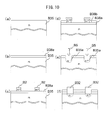
- a diffusion mask layer (B72) is formed on a semiconductor substrate (B65) ( Figs. 13(a) and (b) ), a hole (B72a) is bored in a selected region of the diffusion mask layer (B72) to expose the semiconductor substrate (B65) ( Fig.
- a doped layer (B65a) is formed through the hole (B72a) in the selected region of the semiconductor substrate by a dopant injection layer (B74) formed of, for example, a doping gas such as phosphorus oxychloride (POCl 3 ) or a coating-type doping agent ( Fig. 13(d) ), the diffusion mask layer (B72) and the dopant injection layer (B74) are removed ( Fig. 13(e) ), a passivation layer (B68) is formed on the semiconductor substrate (B65) having the doped layer (B65a) ( Fig.
- a dopant injection layer B74 formed of, for example, a doping gas such as phosphorus oxychloride (POCl 3 ) or a coating-type doping agent
- a hole (B68a) is bored in a selective region of the passivation layer (B68) corresponding to the doped layer (B65a) to expose the semiconductor substrate (B65), and an electrode (B62) is formed through the hole (B68a) to thereby establish electrical contact between the doped layer (B65a) and the electrode (B62) in the selected region of the semiconductor substrate.
- the p-type doped layer is formed similarly to the n-type doped layer by repeating the steps of Figs. 13(b) to (e) .
- Patent Documents 6 and 7 For boring a hole in the diffusion mask layer and the passivation layer, a photolithography, a laser or the like has been heretofore used (Patent Documents 6 and 7).
- a dopant composition containing a dopant is coated on a semiconductor substrate, and the resulting semiconductor substrate is heated in a furnace to diffuse the dopant into the semiconductor substrate.
- heating in a furnace requires a high-temperature treatment for a long time and disadvantageously costs highly. Therefore, in recent years, a technique for diffusing a dopant into a semiconductor substrate from a dopant composition by laser irradiation is being aggressively developed.
- Patent Document 9 discloses that heating in an electric furnace or by laser irradiation can be utilized when diffusing a dopant by using a dopant composition containing a silicon compound such as silicon oxide.
- Patent Document 10 for achieving dopant diffusion by laser irradiation, it is proposed to form a carbon-containing light-absorbing layer on a transparent substrate and put the light-absorbing layer into tight contact with a dopant composition layer.
- Non-Patent Document 1 proposes forming a silicon nitride layer for passivation and anti-reflection on a dopant composition layer and irradiating the silicon nitride film with a laser, thereby injecting a dopant into a semiconductor substrate.
- Non-Patent Document 1 Laser process for selective emitter silicon solar cells ( International Journal of Photoenergy, Volume 2012, 413863 )
- the silicon layer obtained by sintering silicon particles also preferably has a flat surface as described above, but such a silicon layer generally has a relatively large convex part on the surface.
- the obtained silicon layer contains relatively small particles (A40a) and relatively large particles (A40b), which are produced by the sintering of particle, and the surface thereof has relatively large unevenness due to the relatively large particles (A40b) out of those particles.
- the obtained silicon layer may lack sufficient continuity, because a portion where sintered particles are not in contact with each other may be produced.
- a first aspect of the present invention provides a semiconductor laminate comprising a substrate having formed thereon a silicon layer with small surface unevenness and high continuity, and a production method of such a semiconductor laminate. Also, the first aspect of the present invention provides a semiconductor laminate comprising a substrate having formed thereon a silicon layer with small surface unevenness and high continuity, wherein an insulating layer is further stacked on the silicon layer, and a production method of such a semiconductor laminate.
- a doped layer is formed in a selected region.
- a second aspect of the present invention provides a method for manufacturing a semiconductor device, which is free from the above-described problems. Also, the second aspect of the present invention provides a semiconductor device obtained by the method of the second aspect of the present invention.
- Patent Documents 9 and 10 use of a dopant composition containing a silicon compound such as silicon oxide or containing carbon is studied.
- the dopant composition containing a silicon compound such as silicon oxide does not absorb light and only the substrate absorbs light, leaving the possibility that the laser irradiation may cause damage to the substrate.
- the carbon used in the light-absorbing layer may diffuse into the substrate during laser irradiation and work out to an undesirable impurity.
- Non-Patent Document 1 requires CVD method or the like using high vacuum so as to deposit a silicon nitride layer for passivation or anti-reflection and has a problem of high cost.
- a third aspect of the present invention provides a dopant composition free from the above-described problems.
- the third aspect of the present invention provides a doped layer obtainable by using the dopant composition of the third aspect of the present invention, a method for forming a doped layer by using the dopant composition of the third aspect of the present invention, and a method for manufacturing a semiconductor device by using the doped layer forming method of the third aspect of the present invention.
- the present inventors have achieved the first aspect of the present invention including the following ⁇ A1> to ⁇ A22>.
- the present inventors have achieved the second aspect of the present invention including the following ⁇ B1> to ⁇ B17>.
- the present inventors have achieved the third aspect of the present invention including the following ⁇ C1> to ⁇ C20>.
- the sintered silicon particle layer on the substrate can have a relatively flat surface and high continuity without an additional step of removing the surface unevenness.
- the sintered silicon particle layer can have a relatively flat surface and high continuity, so that when an insulating layer, an electrode or the like is deposited thereon, a semiconductor device having good properties can be obtained.
- a doped layer (sometimes referred to as "diffusion layer”) can be formed in a selected region through a relatively small number of steps, and the passivation layer in the region corresponding to the doped layer can be at least partially removed.
- a semiconductor device having a doped layer only in a selected region for example, a solar cell, particularly a back-contact solar cell and a PERL solar cell, can be manufactured through a relatively small number of steps.
- a dopant injection layer can be easily film-formed by coating, and a dopant can be effectively diffused into the substrate by irradiating the obtained dopant injection layer with light such as green laser (wavelength: 532 nm).
- light such as green laser (wavelength: 532 nm).
- an undesired impurity can be prevented from diffusing together with a dopant by not allowing the light-absorbing particles to contain such an undesired impurity.
- the method of the first aspect of the present invention for producing a semiconductor laminate having a substrate and a sintered silicon particle layer on the substrate comprises the following steps (a) to (d):
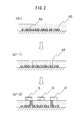
- a silicon particle dispersion containing a dispersion medium and silicon particles dispersed in the dispersion medium is coated on a substrate (A10) to form a silicon particle dispersion layer (A1) (see Fig. 1(a) ).
- the silicon particles contained in the silicon particle dispersion are not limited if it is particles composed of silicon, as long as the object and effects of the first aspect of the present invention are not impaired.
- silicon particles silicon particles described, for example, in Patent Documents 4 and 5 may be used.
- the silicon particles include silicon particles obtained by a laser pyrolysis process, particularly, a laser pyrolysis process using a CO 2 laser.
- the particles of the dispersion may preferably have a relatively small particle diameter so as to form a semiconductor laminate having a flat surface by melting and sintering the particles through light irradiation.
- the average primary particle diameter of the particles may be 1 nm or more, 3 nm or more, 5 nm or more, 10 nm or more, or 15 nm or more.
- the average primary particle diameter of the particles may be 100 nm or less, 40 nm or less, 30 nm or less, 20 nm or less, or 10 nm or less.
- the average primary particle diameter of the present invention can be determined as the number average primary particle diameter by directly measuring the particle diameter based on an image photographed on observation by a Scanning Electron Microscope (SEM), a Transmission Electron Microscope (TEM) or the like, and analyzing particles with an aggregation number of 100 or more.
- SEM Scanning Electron Microscope
- TEM Transmission Electron Microscope
- the silicon particles may be doped with a p-type or n-type dopant.
- the p-type or n-type dopant is selected, for example, from the group consisting of boron (B), aluminum (Al), gallium (Ga), indium (In), titanium (Ti), phosphorus (P), arsenic (As), antimony (Sb) and a combination thereof.
- the degree to which the silicon particles is doped can be determined depending on the desired dopant concentration or the like in the sintered silicon particle layer as the dopant injection layer and in the substrate.
- the particles can contain the dopant at a concentration of 1 ⁇ 10 18 atoms/cm 3 or more, 1 ⁇ 10 19 atoms/cm 3 or more, 1 ⁇ 10 20 atoms/cm 3 or more, 5 ⁇ 10 20 atoms/cm 3 or more, or 1 ⁇ 10 21 atoms/cm 3 or more.
- the dispersion medium of the dispersion is not limited as long as the object and effects of the first aspect of the present invention are not impaired, and, for example, an organic solvent incapable of reacting with the silicon particles for use in the first aspect of the present invention can be used.
- the dispersion medium may be a non-aqueous solvent, for example, an alcohol, an alkane, an alkene, an alkyne, a ketone, an ether, an ester, an aromatic compound or a nitrogen-containing ring compound, particularly, isopropyl alcohol (IPA), N-methyl-2-pyrrolidone (NMP), terpineol or the like.
- IPA isopropyl alcohol
- NMP N-methyl-2-pyrrolidone
- terpineol terpineol
- the dispersion medium is preferably a dehydrated solvent.
- the substrate for use in the method of the first aspect of the present invention is not limited as long as the object and effects of the first aspect of the present invention are not impaired.
- a silicon substrate, a glass substrate or a polymer substrate can be used as the substrate.
- a sintered silicon particle layer having a relatively flat surface and high continuity can be obtained even on a substrate, especially on a glass substrate, where a sintered silicon particle layer having a flat surface and high continuity can be hardly obtained.
- the thickness of the silicon particle dispersion layer obtained in the step (a) can be arbitrarily determined according to the thickness of the sintered silicon particle layer that is desired to be finally obtained.
- the silicon particle dispersion layer 1 is dried to form a green silicon particle layer (A2) (see Fig. 1(b) ).
- the green silicon particle layer may be a single layer or may be formed by stacking a plurality of layers.
- the green silicon particle layer of the step (b) may be a laminate obtained by stacking, in order, a green silicon particle layer containing a p-type dopant, a green silicon particle layer containing substantially no dopant, and a green silicon particle layer containing an n-type dopant, and in this case, a sintered silicon particle layer having a p-i-n structure can be obtained at a time by sintering the laminate.
- the drying is not particularly limited if it is a method capable of substantially removing the dispersion medium from the dispersion, and, for example, the drying may be performed by placing the substrate with the dispersion on a hot plate or in a heating atmosphere.
- the drying temperature can be selected, for example, so as not to cause deterioration or the like of the substrate or the particles of the dispersion and may be selected to be, for example, 50°C or more, 70°C or more, or 90°C or more, and be 100°C or less, 150°C or less, 200°C or less, or 250°C or less.
- a light-transmitting layer (A3) is stacked on the green silicon particle layer (A2) (see Fig. 1(c) ).
- the light-transmitting layer may be any layer enabling the green silicon particle layer to be irradiated with light through the light-transmitting layer during light irradiation in the step (d).
- the light-transmitting layer is a layer where the transmittance for the irradiated light in the step (d), that is, the ratio of light flux of transmitted light to the incident light, is 80% or more, 85% or more, 90% or more, 95% or more, 98% or more, or 99% or more.
- the light-transmitting layer is a layer where the total light transmittance measured in conformity with JIS K7361-1 has such a value.
- the material and properties such as thickness of the light-transmitting layer are not limited as long as the object and effects of the first aspect of the present invention are not impaired, and these can be determined based on the transmittance for irradiated light in the step (d), the ability to flatten the sintered silicon particle layer, and the properties of this layer desired to remain in the obtained semiconductor laminate.
- the material of such a light-transmitting layer may be any of an organic compound, an inorganic compound and an organic-inorganic hybrid compound and particularly, may be a silicon compound.
- the silicon compound includes silicon oxide, silicon nitride, and a compound having a siloxane bond.
- any method such as gas phase method and liquid phase method can be used.
- the gas phase method specifically includes a chemical vapor deposition method (CVD) and a physical vapor deposition method (PVD), and the liquid phase method includes a solution method.
- CVD chemical vapor deposition method
- PVD physical vapor deposition method
- the light-transmitting layer may be a so-called spin-on-glass (SOG) layer.
- SOG spin-on-glass
- an organosilicon compound is mixed with a solvent to form a spin-on-glass solution, the solution is applied to a substrate by spin coating or the like, and thereafter, the organosilicon compound is dehydrated and condensed by heating.
- the organosilicon compound that can be used for the formation of the spin-on-glass layer includes an alkoxysilane, a silanol, a siloxane, a silicate and the like.
- the material of the light-transmitting layer may have a volume resistivity of, for example, 10 10 ⁇ cm or more, 10 11 ⁇ cm or more, 10 12 ⁇ cm or more, 10 13 ⁇ cm or more, or 10 14 ⁇ cm or more.
- a volume resistivity of, for example, 10 10 ⁇ cm or more, 10 11 ⁇ cm or more, 10 12 ⁇ cm or more, 10 13 ⁇ cm or more, or 10 14 ⁇ cm or more.
- the thickness of the light-transmitting layer may be, for example, 50 nm or more, 100 nm or more, 200 nm or more, or 300 nm or more, and 1,000 nm or less, 900 nm or less, 800 nm or less, or 700 nm or less.
- the green silicon particle layer (A2) is irradiated with light (A15) through the light-transmitting layer (A3) to sinter the silicon particles constituting the green silicon particle layer (A2), and thereby form a sintered silicon particle layer (A5) (see Figs. 1(d) , (d1) and (d2).
- the light-transmitting layer is a layer that substantially transmits the irradiated light. Therefore, when the green silicon particle layer is irradiated with light, the substantial portion of irradiated light is transmitted by the light-transmitting layer and reaches the green silicon particle layer, whereby the silicon particles can be sintered.
- the light-transmitting layer stacked in the step (c) may be retained after light irradiation of the step (d) (see Fig. 1(d1) ) or may be removed by light irradiation of the step (d) (see Fig. 1(d2) ).
- the light-transmitting layer is retained after light irradiation of the step (d). However, even when the light-transmitting layer is retained after light irradiation of the step (d), the light-transmitting layer may be partially or completely removed to expose the sintered silicon particle layer.
- a top-gate top-contact thin transistor can be manufactured by producing a semiconductor laminate having a substrate and a sintered silicon particle layer on the substrate by the method of the first aspect of the present invention, then removing a part of the light-transmitting layer from the semiconductor laminate to form an opening part (A7) reaching the sintered silicon particle layer, providing the opening parts (A7) with a source electrode S and a drain electrode D, and forming a gate electrode G on the light-transmitting layer (see Fig. 2 (d1-1)).
- an electrode reaching the sintered silicon particle layer can be formed by producing a semiconductor laminate having a substrate and a sintered silicon particle layer on the substrate by the method of the first aspect of the present invention, then forming an electrode on the light-transmitting layer, and applying a so-called fire-through technique of causing the electrode to penetrate the light-transmitting layer by heating.
- a so-called fire-through technique of causing the electrode to penetrate the light-transmitting layer by heating can be used in a solar cell.
- the light-transmitting layer is removed by light irradiation of the step (d), because the later step of removing the light-transmitting layer can be made unnecessary. Also, in the case where the light-transmitting layer is removed by light irradiation of the step (d), another layer can be optionally stacked on the sintered silicon particle layer.
- the sintered silicon particle layer obtained after light irradiation of the step (d) may have any thickness according to the intended use and may have, for example, a film thickness of 50 nm or more, 100 nm or more, or 200 nm or more, and 1,000 nm or less, 800 nm or less, 500 nm or less, or 300 nm or less.
- any light can be used if formation of the above-described sintered silicon particle layer can be achieved.
- laser light composed of a single wavelength, particularly, laser light having a wavelength of 800 nm or less, 700 nm or less, 600 nm or less, 500 nm or less, or 400 nm or less, and 300 nm or more, can be used as the irradiated light.
- irradiation of the green silicon particle layer with light can also be performed using a flash lamp such as xenon flash lamp that emits light in the wavelength range of a specific band (for example, from 200 to 1,100 nm) at a time.
- light such as pulsed light and continuously oscillating light can be optionally used if formation of the above-described sintered silicon particle layer can be achieved.
- the number of pulsed light irradiations may be 1 or more, 2 or more, 5 or more, or 10 or more, and 300 or less, 200 or less, or 150 or less.
- the irradiation energy of pulsed light may be, for example, 15 mJ/ (cm 2 ⁇ shot) or more, 50 mJ/(cm 2 ⁇ shot) or more, 100 mJ/(cm 2 ⁇ shot) or more, 200 mJ/(cm 2 ⁇ shot) or more, 300 mJ/(cm 2 ⁇ shot) or more, 350 mJ/(cm 2 ⁇ shot) or more, 400 mJ/(cm 2 ⁇ shot) or more, 500 mJ/(cm 2 ⁇ shot) or more, 600 mJ/(cm 2 ⁇ shot) or more, or 700 mJ/(cm 2 ⁇ shot) or more.
- the irradiation energy may be 5,000 mJ/(cm 2 ⁇ shot) or less, 4,000 mJ/(cm 2 ⁇ shot) or less, 3,000 mJ/(cm 2 ⁇ shot) or less, 2,000 mJ/(cm 2 ⁇ shot) or less, 1,500 mJ/(cm 2 ⁇ shot) or less, 1,000 mJ/(cm 2 ⁇ shot) or less, 800 mJ/(cm 2 ⁇ shot) or less, or 600 mJ/(cm 2 ⁇ shot) or less.
- the irradiation time of pulsed light may be, for example, 200 nanoseconds/shot or less, 100 nanoseconds/shot or less, or 50 nanoseconds/shot or less.
- the processing time may be prolonged.
- the optimal conditions such as irradiation energy and number of irradiations are dependent on, for example, the wavelength of light irradiation used or the properties of particle, and one skilled in the art can determine the optimal value by performing an experiment with reference to the description of the present invention.
- the light irradiation for sintering the dispersion particles is preferably performed in a non-oxidizing atmosphere, for example, an atmosphere composed of hydrogen, a rare gas, nitrogen or a combination thereof, so as to prevent oxidation of the dispersion particle.
- a non-oxidizing atmosphere for example, an atmosphere composed of hydrogen, a rare gas, nitrogen or a combination thereof.
- a light-transmitting layer is stacked on the green silicon particle layer and since the green silicon particle layer is thereby isolated from the atmosphere, the light irradiation can also be performed in an oxidizing atmosphere such as atmospheric atmosphere.
- the rare gas includes, particularly argon, helium and neon.
- hydrogen has an action of reducing the dispersion particles and for forming a continuous layer by reducing the oxidized surface portion, it may be preferred that the atmosphere contains hydrogen.
- the oxygen content in the atmosphere may be 1 vol% or less, 0.5 vol% or less, 0.1 vol% or less, or 0.01 vol% or less.
- the semiconductor laminate of the first aspect of the present invention has a substrate and a sintered silicon particle layer on the substrate and is produced by the method of the first aspect of the present invention.
- the semiconductor laminate of the first aspect of the present invention has, for example, (a) a substrate, (b) a sintered silicon particle layer stacked on the substrate and formed of silicon particles, and (c) a light-transmitting layer stacked on the sintered silicon particle layer.
- the semiconductor laminate of the first aspect of the present invention has, for example, (a) a glass substrate and (b) a sintered silicon particle layer stacked directly on the glass substrate and formed of silicon particles, the sintered silicon particle layer having an arithmetic mean roughness of 100 nm or less, 90 nm or less, 80 nm or less, 70 nm or less, 60 nm or less, 50 nm or less, or 40 nm or less.
- the green silicon laminate of the first aspect of the present invention may be irradiated with light.
- the green silicon laminate of the first aspect of the present invention may have (a) a substrate, (b) a green silicon particle layer stacked on the substrate and formed of silicon particles, and (c) a light-transmitting layer stacked on the green silicon particle layer.
- the semiconductor device of the first aspect of the present invention has the semiconductor laminate of the first aspect of the present invention.
- the semiconductor device of the first aspect of the present invention is a field-effect transistor such as top-gate top-contact thin-film transistor or a solar cell, by virtue of having a silicon layer with small surface unevenness and high continuity, stable properties can be provided when an insulating layer, an electrode or the like is deposited on the silicon layer.
- the method of the second aspect of the present invention for manufacturing a semiconductor device comprises forming a first doped layer in a first region of a semiconductor layer or substrate by the following steps.
- a laminate having the following (i) and (ii) is provided: (i) first and/or second passivation layers disposed on the semiconductor layer or substrate, and (ii) a first dopant injection layer disposed in the region corresponding to the first region above the first passivation layer but below the second passivation layer, in which the dopant injection layer is composed of first particles and the first particles are substantially formed of the same element as the semiconductor layer or substrate and is doped with a p-type or n-type dopant.
- the region corresponding to the first dopant injection layer of the laminate is irradiated with light, thereby doping the first region with the p-type or n-type dopant to form the first doped layer and at least partially removing the region corresponding to the dopant injection layer out of the first dopant injection layer and the passivation layer.
- the concentration of the dopant at a depth of 0.1 ⁇ m from the surface of said first region may be 1 ⁇ 10 17 atoms/cm 3 or more, 1 ⁇ 10 18 atoms/cm 3 or more, 1 ⁇ 10 19 atoms/cm 3 or more, or 1 ⁇ 10 20 atoms/cm 3 or more.
- the semiconductor device manufactured by the method of the second aspect of the present invention may be a solar cell or a thin-layer transistor.
- the solar cell may be a back-contact solar cell or a PERL solar cell, and the first region may be on the back surface side of the semiconductor layer or substrate.
- a passivation layer (B18) is deposited on a semiconductor substrate (B15) ( Figs. 8(a) and (b) ), a first dispersion containing first particles is applied to the region corresponding to the first region of the first passivation layer (B18), the dispersion is dried to form a first dopant injection layer (B2) ( Fig.
- the first dopant injection layer (B2) is irradiated with light (B5), thereby doping the first region with a p-type or n-type dopant to form a first doped layer (B15a) and at least partially removing the region corresponding to the first dopant injection layer (B2) out of the first dopant injection layer (B2) and the first passivation layer (B18) ( Fig. 8(d) ), and an electrode (B12) is optionally formed through the passivation layer (B18) to come into contact with the first doped layer (B15a) ( Fig. 8(e) ).
- a second dispersion containing second particles is applied to a second region of the semiconductor layer or substrate, simultaneously with application of the first dispersion, between application and drying of the first dispersion, between drying of the first dispersion and removal of the first dopant injection layer, or after removal of the first dopant injection layer.
- the second dispersion applied is dried simultaneously with drying of the first dispersion or separately from drying of the first dispersion, thereby forming a second dopant injection layer, and the second dopant injection layer is irradiated with light simultaneously with light irradiation of the first dopant injection layer or separately from light irradiation of the first dopant injection layer, thereby doping the second region of the semiconductor layer or substrate with the p-type or n-type dopant to form the second doped layer and at least partially removing the region corresponding to the second dopant injection layer out of the second dopant injection layer and the first and/or second passivation layers.
- the particles doped with a p-type dopant and the particles doped with an n-type dopant can be collectively sintered by light irradiation or collectively sintered by drying and light irradiation.
- a processing of performing application of the dispersion by using a printing method such as inkjet printing and screen printing without using photolithography may be particularly beneficial to the shortening of production process.
- the second particles are substantially formed of the same element as the semiconductor layer or substrate, and are doped with a dopant of a type different from the dopant of the first particle.
- the description of the present invention regarding the first doped layer may be referred to, and in particular, as for the production method of the second dopant injection layer, the doping concentration and the like, the description of the present invention regarding the first dopant injection layer may be referred to.
- a first dispersion containing first particles is applied to the first region of the semiconductor substrate (B25), the dispersion is dried to form a first dopant injection layer (B2) ( Figs. 9(a) and (b) ), a second passivation layer (B28) is deposited on the first dopant injection layer (B2) ( Fig.
- the region corresponding to the first dopant injection layer (B2) of the second passivation layer (B28) is irradiated with light (B5), thereby doping the first region of the semiconductor substrate with a p-type or n-type dopant to form a first doped layer (B25a) and at least partially removing the region corresponding to the first dopant injection layer (B2) out of the first dopant injection layer (B2) and the second passivation layer (B28) ( Fig. 9(d) ), and an electrode (B22) is optionally formed through the second passivation layer (B28) to come into contact with the first doped layer (B25a) ( Fig. 9(e) ).
- the second region of the semiconductor substrate can be doped with a p-type or n-type dopant by using the second dispersion.
- a first passivation layer (B38a) is deposited on a semiconductor substrate (B35) ( Figs. 10(a) and (b) ), a first dispersion containing first particles is applied to the region corresponding to the first region out of the first passivation layer (B38a), the dispersion is dried to form a first dopant injection layer (B2) ( Fig. 10(c) ), a second passivation layer (B38b) is deposited on the first passivation layer (B38a) and the first dopant injection layer (2) ( Fig.
- the region corresponding to the first dopant injection layer (B2) out of the second passivation layer (B38b) is irradiated with light (B5), thereby doping the first region of the semiconductor substrate with a p-type or n-type dopant to form a first doped layer (B35a) and at least partially removing the region corresponding to the first doped layer (B35a) out of the first dopant injection layer (B2) and the first and second passivation layers (B38a, B38b) ( Fig. 10(e) ), and an electrode (B32) is optionally formed through the first and second passivation layers (B38a, B38b) to come into contact with the first doped layer (B35a) ( Fig. 10(f) ).
- the second region of the semiconductor substrate can be doped with a p-type or n-type dopant by using the second dispersion.
- the semiconductor layer or substrate that can be used in the second aspect of the present invention, any semiconductor layer or substrate composed of a semiconductor element may be employed.
- silicon, germanium, or a combination thereof may be used as the semiconductor element.
- the semiconductor layer or substrate includes a silicon wafer, a gallium wafer, an amorphous silicon layer, an amorphous gallium layer, a crystalline silicon layer, and a crystalline gallium layer.
- the semiconductor layer or substrate may be doped with the same dopant element as that of the particles contained in the dispersion, at a concentration lower than in the particle.
- the semiconductor layer or substrate may be entirely or partially doped in advance.
- the passivation layer that can be used in the method of the second aspect of the present invention may have any thickness enabling the layer to function as a passivation layer, and the thickness may be, for example, 1 nm or more, 5 nm or more, 10 nm or more, 30 nm or more, or 50 nm or more. Also, the thickness may be 300 nm or less, 200 nm or less, 100 nm or less, 50 nm or less, 30 nm or less, 20 nm or less, or 10 nm or less. If the thickness is too small, the property as the passivation layer may be poor, or if the thickness is too large, the layer may not be removed by light irradiation.
- the passivation layer is a first passivation layer, that is, in the case of depositing a dopant injection layer on the passivation layer and not only forming a first doped layer by doping the first region with a dopant through light irradiation but also removing the dopant injection layer and the region corresponding to the dopant injection layer of the passivation layer, if the thickness of the passivation layer is too large, injection of the dopant into the semiconductor layer or substrate may become insufficient.
- the passivation layer may be formed of any material enabling the layer to function as a passivation layer and may be formed, for example, a material selected from the group consisting of silicon nitride (SiN), silicon oxide (SiO 2 ), aluminum oxide (Al 2 O 3 ) and a combination thereof.
- Application of the dispersion in the method of the second aspect of the present invention for manufacturing a semiconductor device is not particularly limited in the method therefor as long as it is a method capable of coating the dispersion with desired thickness and uniformity, and the application may be performed, for example, an inkjet printing method, a spin coating method or a screen printing method.
- application using a printing method such as inkjet printing and screen printing may be useful for applying the dispersion to a specific region and shortening the production process.
- the coating may be performed such that the thickness of the dopant injection layer obtained by drying the dispersion layer is 10 nm or more, 30 nm or more, 50 nm or more, 100 nm or more, or 200 nm or more, and 2,000 nm or less, 1,000 nm or less, 500 nm or less, or 300 nm or less.
- the thickness of the dopant injection layer can be determined by taking into account, for example, the degree of doping of the doped layer in the obtained semiconductor device, the thickness of the dope injection layer removable by a laser, or the thickness of the dope injection layer allowed to remain on the semiconductor substrate or layer.
- the thickness of the dopant injection layer is not particularly limited as long as the effects of the second aspect of the present invention are obtained.
- the dispersion medium of the dispersion is not limited as long as the object and effects of the second aspect of the present invention are not impaired, and, for example, an organic solvent incapable of reacting with the particles for use in the second aspect of the present invention can be used.
- the dispersion medium may be a dispersion medium recited in the first aspect of the present invention, such as isopropyl alcohol (IPA).
- the particles of the dispersion are not limited if it is particles composed of the same element as the semiconductor layer or substrate and is doped with a p-type or n-type dopant, as long as the object and effects of the second aspect of the present invention are not impaired.
- Such particles include, for example, a silicon or germanium particles disclosed in Patent Documents 4 and 5.
- the silicon or germanium particles includes silicon or germanium particles obtained by a laser pyrolysis process, particularly, a laser pyrolysis process using a CO 2 laser.
- the crystallization degree of particles is relatively low and/or the particle diameter of particles is relatively small.
- the average primary particle diameter of the particles may be 1 nm or more, 3 nm or more, 5 nm or more, 10 nm or more, or 15 nm or more.
- the average primary particle diameter of the particles may be 100 nm or less, 50 nm or less, 40 nm or less, 30 nm or less, 20 nm or less, or 10 nm or less.
- the average primary particle diameter of the particles can be determined as described in the first aspect of the present invention.
- the average primary particle diameter of the silicon particles was determined by performing TEM observation and analyzing the image at a magnification of 100,000. Based on an aggregate of n number of 500 or more, the average primary particle diameter and dispersion of the silicon particle dispersion were calculated.
- the dopant for doing the particles of the dispersion may be either a p-type or n-type dopant and is selected, for example, from dopants recited in the first aspect of the present invention.
- the degree of doping of the particles of the dispersion can be determined depending on the desired dopant concentration or the like in the dopant injection layer and the semiconductor layer or substrate.
- the dopant concentration may be, for example, the dopant concentration given in the first aspect of the present invention.
- the dopant concentration may be, for example, 1 ⁇ 10 22 atoms/cm 3 or less, or 1 ⁇ 10 21 atoms/cm 3 or less.
- Drying in the method of the second aspect of the present invention for manufacturing a semiconductor device is not particularly limited as long as it is a method capable of substantially removing the dispersion medium from the dispersion, and drying can be performed, for example, by placing the substrate with the dispersion on a hot plate or in a heating atmosphere.
- the drying temperature can be selected, for example, so as not to cause deterioration or the like of the substrate or the particles of the dispersion and may be selected to be, for example, 50°C or more, 70°C or more, 90°C or more, and 100°C or less, 200°C or less, 300°C or less, 400°C or less, 500°C or less, 600°C or less, 700°C or less, or 800°C or less.
- Light irradiation in the method of the second aspect of the present invention for manufacturing a semiconductor device may be any light irradiation capable of diffusing the p-type or n-type dopant contained in the dopant injection layer into the selected region of the semiconductor layer or substrate and at the same time, at least partially removing the region corresponding to the first dopant injection layer out of the first dopant injection layer and the first and/or second passivation layers.
- the expression "at least partially removing” means that at least a part of the dopant injection layer and the first and/or second passivation layers is removed, and encompasses not only a case where such a layer is removed by the removal to an extent enabling formation of an electrode directly on the doped layer but also a case where the remaining layer such as dopant injection layer needs to be further removed by another treatment such as etching and cleaning.
- the dopant injection layer, passivation layer and surface portion of the below-located semiconductor layer or substrate are rapidly cooled due to transfer of heat to the main body portion of the semiconductor layer or substrate. Therefore, in the method of the second aspect of the present invention, the first region can be doped with the p-type or n-type dopant to form a doped layer without exposing the main body portion of the semiconductor layer or substrate to high heat.
- any light can be employed if doping or the like of a specific region of the semiconductor layer or substrate can be achieved as above.
- laser light composed of a single wavelength can be used as the irradiated light.
- it is effective to perform the irradiation by using light at a wavelength which is absorbed by Si.
- the optimal conditions such as irradiation energy and number of irradiations are dependent on, for example, the wavelength of light irradiation used or the properties of particle, and one skilled in the art can determine the optimal value by performing an experiment with reference to the description of the present invention.
- the light irradiation for sintering the dispersion particles is preferably performed in a non-oxidizing atmosphere, for example, an atmosphere composed of hydrogen, a rare gas, nitrogen or a combination thereof, so as to reduce the effect on the properties of the semiconductor device.
- a non-oxidizing atmosphere for example, an atmosphere composed of hydrogen, a rare gas, nitrogen or a combination thereof, so as to reduce the effect on the properties of the semiconductor device.
- description in the first aspect of the present invention can be referred to.
- hydrogen has an action of reducing the dispersion particles and for forming a continuous layer by reducing the oxidized surface portion, it may be preferred that the atmosphere contains hydrogen.
- a passivation layer is stacked on the semiconductor substrate or layer; in a first region of the semiconductor substrate or layer, the passivation layer is at least partially removed, first particles is sintered to the semiconductor substrate or layer, and a first electrode reaching the first region through the passivation layer is formed via the first particle; the first particles is substantially formed of the same element as the semiconductor layer or substrate and is doped with a p-type or n-type dopant; and the concentration of the dopant is 1 ⁇ 10 17 atoms/cm 3 or more at a depth of 0.1 ⁇ m from the surface of the first region.
- the passivation layer in a second region of the semiconductor substrate or layer, is at least partially removed, second particles is sintered to the semiconductor substrate or layer, and a second electrode reaching the second region through the passivation layer is formed via the second particle;
- the second particles is substantially formed of the same element as the semiconductor layer or substrate and is doped with a dopant of a type different from the dopant of the first particle; and the concentration of the dopant is 1 ⁇ 10 17 atoms/cm 3 or more at a depth of 0.1 ⁇ m from the surface of the second region.
- This semiconductor device is, for example, a solar cell or a thin-layer transistor.
- the semiconductor device of the second aspect of the present invention is not particularly limited in its manufacturing method but can be obtained, for example, by the method of the second aspect of the present invention.
- descriptions regarding the method of the second aspect of the present invention for manufacturing a semiconductor device can be referred to.
- the dopant composition of the third aspect of the present invention contains a solvent, a dopant compound having a dopant element, and light-absorbing particles composed of a material having at least one peak absorption wavelength in the range of 100 to 1,000 nm.
- a dopant injection layer (C22) on a semiconductor substrate (C30) by using the dopant composition of the third aspect of the present invention upon irradiation with light (C10) such as green laser (wavelength: 532 nm), the light-absorbing particles in the dopant injection layer (C22) absorbs at least a part of the irradiated light (C10) to heat the layer, and the below-located semiconductor substrate (C30) optionally absorbs the remainder (C10a) of light to heat the substrate, whereby diffusion of the dopant from the dopant injection layer (C22) into the semiconductor substrate (C30) is promoted.
- light such as green laser (wavelength: 532 nm
- the conventional dopant composition does not contain light-absorbing particles and in turn, the obtained dopant injection layer (C23) does not contain a light-absorbing particle. Therefore, in the conventional technique, as shown in Fig. 17(b) , upon irradiation with light (C10), light passes through the conventional dopant injection layer (C23) but only the below-located semiconductor substrate (C30) absorbs light to heat the substrate, and the heat of the semiconductor substrate (C30) transfers to the conventional dopant injection layer (C23) to heat the dopant injection layer (C23), whereby diffusion of the dopant from the dopant injection layer (C23) into the semiconductor substrate (C30) is promoted.
- the dopant injection layer does not contain a light-absorbing particle
- light passes through the dopant injection layer and is absorbed only by the below-located semiconductor substrate, and there is the possibility of, for example, producing a defect in the semiconductor substrate by light irradiation or deteriorating the semiconductor substrate due to heat.
- the dopant composition of the third aspect of the present invention at least a part of the irradiated light is absorbed by the dopant injection layer, whereby occurrence of the above-described problem can be suppressed.
- the solvent is not limited as long as the object and effects of the third aspect of the present invention are not impaired, and, for example, an organic solvent incapable of reacting with the particles for use in the dopant composition can be used.
- the solvent may be a solvent such as isopropyl alcohol (IPA) recited as the dispersion medium in the present invention.
- the material constituting the light-absorbing particles for use in the dopant composition of the third aspect of the present invention has at least one peak absorption wavelength in the range of 100 to 1,000 nm, for example, from 200 to 1,000 nm, from 200 to 800 nm, or from 200 to 600 nm.
- the peak at the peak absorption wavelength may be a maximum peak in the range of 100 to 2,500 nm or from 200 to 2,500 nm.
- the light-absorbing particles are composed of, for example, a metal or half metal element, particularly, silicon, germanium or a combination thereof.
- the metal or half metal element generally has an absorption peak in the visible region, and therefore can be used as the light-absorbing particles in the dopant composition of the third aspect of the present invention.
- the silicon has an absorption peak in the range of 200 to 400 nm.
- a metal oxide such as silicon oxide does not have an absorption peak in the visible region, and therefore cannot be used as the light-absorbing particle.
- metal oxide particles can be used as the light-absorbing particles of the third aspect of the present invention if it has at least one peak absorption wavelength in the range of 100 to 1,000 nm.
- Such a light-absorbing particle particularly, silicon particles or a germanium particle
- a laser pyrolysis process particularly, a laser pyrolysis process using a CO 2 laser.
- the light-absorbing particles are composed of, for example, the same element as the semiconductor substrate that is doped using the dopant composition of the third aspect of the present invention. Accordingly, for example, when the semiconductor substrate is composed of silicon, germanium or a combination thereof, the light-absorbing particles may be composed of silicon, germanium or a combination thereof. Constituting the light-absorbing particles by the same element as the semiconductor substrate may be preferred for preventing contamination of the semiconductor substrate with the light-absorbing particle.
- the light-absorbing particles may contain substantially no dopant or may be doped with a dopant.
- the expression "contain substantially no dopant” means that a doping element is not intentionally added, and in other words, means that the particles may contain a very slight amount of an unintentionally mixed dopant.
- the particles may be doped with either a p-type or n-type dopant.
- This dopant is selected, for example, from dopants recited in the first aspect of the present invention.
- the degree of doping of the light-absorbing particles can be determined depending on, for example, the concentration of the dopant compound contained in the dopant composition or the desired dopant concentration in the semiconductor substrate.
- the dopant concentration of the light-absorbing particles may be, for example, the dopant concentration given in the first aspect of the present invention.
- the light-absorbing particles may have an average primary particle diameter of, for example, 1 nm or more, 3 nm or more, 5 nm or more, 10 nm or more, or 15 nm or more. Also, the light-absorbing particles may have an average primary particle diameter of, for example, 100 nm or less, 50 nm or less, 40 nm or less, 30 nm or less, 20 nm or less, or 10 nm or less. A relatively small particle diameter of the light-absorbing particles may be preferred, because the dopant injection layer containing the light-absorbing particles is uniformly heated by light irradiation.
- the content of the light-absorbing particles in the dopant composition of the third aspect of the present invention may be determined by taking into account, for example, the light absorptivity of the light-absorbing particles for the wavelength of light used or the handleability of the dopant composition.
- the dopant composition of the third aspect of the present invention may contain the light-absorbing particles in an amount of, for example, 0.1 mass% or more, 0.5 mass% or more, 1.0 mass% or more, 2 mass% or more, or 3 mass% or more.
- the dopant compound for use in the dopant composition of the third aspect of the present invention has a dopant element.
- the dopant element may be either p-type or n-type.
- This dopant element may be the dopant element recited above with respect to the light-absorbing particle, for example, boron (B) or phosphorus (P).
- the dopant compound may be specifically any compound capable of injecting a dopant element into the semiconductor substrate when heated in the dopant injection layer, and a compound employed in general for this purpose may be used.
- the dopant compound having an n-type dopant includes, for example, P 2 O 5 , a phosphoric acid ester such as dibutyl phosphate, tributyl phosphate, monoethyl phosphate, diethyl phosphate, triethyl phosphate, monopropyl phosphate and dipropyl phosphate, Bi 2 O 3 , Sb (OCH 2 CH 3 ) 3 , SbCl 3 , H 3 AsO 4 , and As(OC 4 H 9 ) 3 .
- the dopant compound having a p-type dopant includes, for example, B 2 O 3 , Al 2 O 3 , and gallium trichloride.
- the concentration of the dopant compound in the dopant composition of the third aspect of the present invention and the ratio between the light-absorbing particles and the dopant compound can be determined by taking into account, for example, the desired doping depth or doping concentration of the doped layer.
- the dopant composition of the third aspect of the present invention may contain, as other components, any other components such as binder resin, surfactant and thickener.
- binder resin for example, ethyl cellulose may be used in view of thixotropy, dispersibility of silicon particle, and the like.
- the first dopant injection layer of the third aspect of the present invention contains a dopant compound having a dopant element and a light-absorbing particles composed of a material having at least one peak absorption wavelength in the range of 100 to 1,000 nm.
- the second dopant injection layer of the third aspect of the present invention has the following layers stacked one on another:
- the dopant compound-containing layer may be stacked on the light-absorbing particle-containing layer ( Fig. 17(c) ), or conversely, the light-absorbing particle-containing layer may be stacked on the dopant compound-containing layer ( Fig. 17(d) ).
- the dopant compound-containing layer may further contain light-absorbing particles composed of a material having a peak absorption wavelength in the range of 100 to 1,000 nm, or the light-absorbing particle-containing layer may further contain a dopant compound having a dopant element. That is, in the second dopant injection layer of the third aspect of the present invention, either one or both of the dopant compound-containing layer and the light-absorbing particle-containing layer may be the dopant composition of the third aspect of the present invention.
- the light-absorbing particles in the light-absorbing particle-containing layer (C26) absorbs at least a part of the irradiated light (C10) to heat the layer
- the below-located semiconductor substrate (C30) optionally absorbs the remainder (C10a) of light passed through the dopant compound-containing layer (C24) to heat the substrate, whereby diffusion of the dopant from the dopant injection layers (C24, C26) into the semiconductor substrate (C30) can be promoted.
- the dopant injection layer of the third aspect of the present invention may be stacked on a semiconductor substrate.
- the semiconductor substrate may be any semiconductor substrate intended to form a dopant injection layer thereon by injecting a dopant.
- the semiconductor substrate may be composed of, for example, silicon, germanium or a combination thereof. Accordingly, the semiconductor substrate includes, for example, a silicon wafer, a germanium wafer, an amorphous silicon layer, an amorphous germanium layer, a crystalline silicon layer, and a crystalline germanium layer.
- the first dopant injection layer of the third aspect of the present invention may be formed by applying, in any manner, the dopant composition of the third aspect of the present invention to the semiconductor substrate and may be formed, for example, by an inkjet method, a spin coating method or a screen printing method.
- the dopant injection layer may be formed using a printing method such as inkjet printing and screen printing, and this processing may be particularly useful for shortening the production process.
- the dopant injection layer having a pattern can be formed by applying the dopant composition by a printing method.
- the second dopant injection layer of the third aspect of the present invention may be formed by applying, in place of the dopant composition of the third aspect of the present invention, the dopant compound-containing composition containing a solvent and a dopant compound and the light-absorbing particle-containing composition containing a solvent and a light-absorbing particle, to the semiconductor substrate.
- the thickness of the obtained dopant injection layer is preferably a thickness making it possible to successfully inject the dopant element from the dopant injection layer into the semiconductor substrate by light irradiation. Accordingly, the thickness may be, for example, 50 nm or more, 100 nm or more, or 200 nm or more, and 5,000 nm or less, 4,000 nm or less, or 3,000 nm or less.
- the dopant injection layer may be optionally dried by a drying step. This drying may be performed in any manner capable of substantially removing the solvent from the dopant injection layer and can be performed, for example, by placing the substrate with the dopant injection layer on a hot plate or in a heating atmosphere.
- the drying temperature in this drying can be selected, for example, so as not to cause deterioration or the like of the semiconductor substrate and the dopant injection layer and may be selected to be, for example, 50°C or more, 70°C or more, or 90°C or more, and be 100°C or less, 150°C or less, 200°C or less, or 250°C or less.
- the method of the third aspect of the present invention for forming a doped layer comprises irradiating the dopant injection layer of the third aspect of the present invention with light to diffuse the dopant element into the semiconductor substrate.
- the light-absorbing particles preferably has, at the main wavelength of the irradiated light, a light absorptivity of 0.05 times or more, or 0.1 times or more, the light absorptivity at the peak absorption wavelength, because the irradiated light is efficiently absorbed and converted to heat.
- Light irradiation may be any light irradiation capable of diffusing the dopant contained in the dopant injection layer into the selected region of the semiconductor substrate.
- any light can be employed if the dopant can be diffused as above.
- laser light composed of a single wavelength can be used as the irradiated light.
- the number of pulsed light irradiations may be, for example, 1 or more, 2 or more, 5 or more, or 10 or more, and 100 or less, 80 or less, or 50 or less.
- the irradiation energy of pulsed light may be, for example, 15 mJ/(cm 2 ⁇ shot) or more, 50 mJ/(cm 2 ⁇ shot) or more, 100 mJ/(cm 2 ⁇ shot) or more, 150 mJ/(cm 2 ⁇ shot) or more, 200 mJ/(cm 2 ⁇ shot) or more, or 300 mJ/(cm 2 ⁇ shot) or more, and 1,000 mJ/(cm 2 ⁇ shot) or less, or 800 mJ/(cm 2 ⁇ shot) or less.
- the irradiation time of pulsed light may be, for example, 200 nanoseconds/shot or less, 100 nanoseconds/shot or less, or 50 nanoseconds/shot or less.
- the number of pulsed light irradiations may be, for example, 1 or more, 5 or more, 10 or more, 25 or more, or 50 or more, and 300 or less, 200 or less, or 100 or less.
- the irradiation energy of pulsed light may be, for example, 100 mJ/(cm 2 ⁇ shot) or more, 300 mJ/(cm 2 ⁇ shot) or more, 500 mJ/(cm 2 ⁇ shot) or more, 900 mJ/(cm 2 ⁇ shot) or more, 1,000 mJ/(cm 2 ⁇ shot) or more, or 1, 300 mJ/(cm 2 ⁇ shot) or more, and 5,000 mJ/(cm 2 ⁇ shot) or less, or 4,000 mJ/(cm 2 ⁇ shot) or less.
- the irradiation time of pulsed light may be, for example, 50 nanoseconds/shot or more, 100 nanoseconds/shot or more, or 150 nanoseconds/shot or more, and 300 nanoseconds/shot or less, 200 nanoseconds/shot or less, or 180 nanoseconds/shot or less.
- the energy per pulse required to achieve the desired dopant diffusion becomes large, leaving the possibility of damage to the dopant injection layer or deterioration of the properties of the semiconductor substrate below the dopant injection layer. Also, if the irradiation energy per pulse is too small, sufficient dopant diffusion into the semiconductor substrate may not occur. Also, even when dopant diffusion into the semiconductor substrate occurs, if the energy is too small, the number of irradiations necessary for obtaining the required cumulative energy is increased, and therefore the processing time may be prolonged.
- the optimal conditions such as irradiation energy and number of irradiations are dependent on, for example, the wavelength of light irradiation used or the properties of light-absorbing particle, and one skilled in the art can determine the optimal value by performing an experiment with reference to the description of the present invention.
- selecting the number of irradiations, irradiation energy and irradiation time of pulsed light in the ranges above may be preferred for achieving dopant diffusion into the semiconductor substrate without causing deterioration of the below-located semiconductor substrate.
- Light irradiation may be performed under the atmosphere but is preferably performed in a non-oxidizing atmosphere according to the material, for example, in an atmosphere composed of hydrogen, a rare gas, nitrogen or a combination thereof, so as to prevent oxidation of the light-absorbing particle.
- the rare gas includes, particularly argon, helium and neon.
- the oxygen content in the atmosphere may be 1 vol% or less, 0.5 vol% or less, 0.1 vol% or less, or 0.01 vol% or less.
- the method of the third aspect of the present invention for manufacturing a semiconductor device comprises forming a doped layer by the method of the third aspect of the present invention.
- the semiconductor device manufactured by the method of the third aspect of the present invention includes a solar cell.
- the semiconductor device of the third aspect of the present invention is manufactured by the method of the third aspect of the present invention for manufacturing a semiconductor device.
- the third aspect of the present invention is not limited to the above-described embodiments, but modification such as various design changes based on the knowledge of one skilled in the art may be made therein, and embodiments to which such modification is added are also included in the scope of the third aspect of the present invention.
- New embodiments resulting from combination of the above-described embodiment and the following modification example have respective effects of the combined embodiment and modification example.
- Example A1 a laminate having the configuration shown in Fig. 1(d1) was obtained. That is, in Example A1, a laminate where a sintered silicon particle layer and a light-transmitting layer are stacked on a substrate was obtained.
- the silicon particles were produced from SiH 4 gas as the raw material by a Laser Pyrolysis (LP) process using a CO 2 laser.
- the obtained silicon particles had an average primary particle diameter of about 7 nm.
- These silicon particles were ultrasonically dispersed in isopropyl alcohol (IPA) to obtain a silicon particle dispersion having a solid content concentration of 3 mass%.
- IPA isopropyl alcohol
- the average primary particle diameter of the silicon particles was calculated based on an aggregate of 500 or more particles by performing TEM observation and analyzing the image at a magnification of 100,000.
- a glass substrate was ultrasonically cleaned for 5 minutes in each of acetone and isopropyl alcohol.
- a few drops of the silicon particle dispersion were dropped on the substrate and spin-coated at 500 rpm over 5 seconds and further at 4,000 rpm over 10 seconds, thereby coating the silicon particle dispersion on the substrate.
- the substrate coated with the silicon particle dispersion was dried on a hot plate at 70°C to remove the isopropyl alcohol as the dispersion medium in the silicon particle dispersion, and thereby obtain a green silicon particle layer (film thickness: 300 nm) containing silicon particles (average primary particle diameter: about 7 nm).
- a film of MSQ (methyl silsesquioxane) as a compound having light transmittability was formed on the substrate coated with the green silicon particle layer. Specifically, a few drops of a solution obtained by dissolving MSQ in propylene glycol monomethyl ether acetate (PGMEA) (solid content concentration: 30 mass%, produced by Honeywell, trade name: PTS R-6) were dropped on the substrate coated with the green silicon particle layer, then spin-coated at 500 rpm over 5 seconds and further at 3,200 rpm over 20 seconds, and dried under heating on a hot plate at 80°C over 5 minutes in an N 2 atmosphere and further at 400°C over 60 minutes in a furnace, whereby the MSQ film was obtained. The film thickness of the obtained MSQ film was 700 nm. The obtained laminate had the configuration shown in Fig. 1(c) .
- the laminate in which the light-transmitting layer was stacked on the green silicon particle layer was irradiated with a YVO 4 laser (wavelength: 355 nm) by using a laser light irradiation apparatus (trade name: Osprey 355-2-0, manufactured by Quantronix) to sinter the silicon particles in the green silicon particle layer, and thereby produce a sintered silicon particle layer.
- the laser irradiation conditions were an irradiation energy of 50 mJ/(cm 2 ⁇ shot) and a number of shots of 20, and laser irradiation was performed in an atmosphere of nitrogen (N 2 ) containing 3.5% hydrogen (H 2 ).
- Fig. 5(a) shows the observation results of FE-SEM.
- the laminate had a configuration where a sintered silicon particle layer (A54) and a light-transmitting layer (A56) are staked on a substrate (A52). That is, the laminate obtained in Example A1-1 had the configuration shown in Fig. 1(d1) .
- the crystallization degree was determined by performing Raman spectroscopic analysis of the sintered silicon particle layer.
- the crystallization degree by Raman spectroscopic analysis is shown in Table 1.
- Sintered silicon particle layers were produced in the same manner as in Example A1-1 except that the laser irradiation energy was changed to 100 mJ/(cm 2 ⁇ shot), 200 mJ/(cm 2 ⁇ shot) and 300 mJ/(cm 2 ⁇ shot) in Examples A1-2 to A1-4, respectively.
- Example A1-2 had the configuration shown in Fig. 1(d1) , that is, a configuration where a sintered silicon particle layer (A5) and a light-transmitting layer (A3) are stacked on a substrate (A10). Also, the laminates obtained in Examples A1-3 and 1-4 had the configuration shown in Fig. 1(d2) , that is, a configuration where only a sintered silicon particle layer (A5) is stacked on a substrate (A10).
- Sintered silicon particle layers were produced in the same manner as in Example A1-1 except that in Examples A2-1 to A2-4, a light-transmitting layer (see below) containing, as the main component, silicon oxide obtained from a silanol solution was used as the light-transmitting layer.
- the laser irradiation energy was changed to 100 mJ/(cm 2 ⁇ shot), 200 mJ/(cm 2 ⁇ shot), 300 mJ/(cm 2 ⁇ shot) and 400 mJ/(cm 2 ⁇ shot) in Examples A2-1 to A2-4, respectively.
- the laminates obtained in Examples A2-1 and A2-2 had the configuration shown in Fig. 1(d1) , that is, a configuration where a sintered silicon particle layer (A5) and a light-transmitting layer (A3) are stacked on a substrate (A10). Also, the laminates obtained in Examples A2-3 and A2-4 had the configuration shown in Fig. 1(d2) , that is, a configuration where only a sintered silicon particle layer (A5) is stacked on a substrate (A10).
- the light-transmitting layer containing, as the main component, silicon oxide used in Examples A2-1 to A2-4 was formed on the substrate coated with the green silicon particle layer by using a silanol solution (OCD Type-7 12000-T (produced by Tokyo Ohka Kogyo Co., Ltd.).
- OCD Type-7 12000-T produced by Tokyo Ohka Kogyo Co., Ltd.
- the coating-type insulating film used as the light-transmitting layer had an ultraviolet-visible transmittance of 99% or more.
- a few drops of the solution above were dropped on the substrate coated with the green silicon particle layer, spin-coated at 5,000 rpm for 15 seconds, and heated/dried at 80°C over 1 minute, then at 150°C over 2 minutes on a hot plate under the atmosphere and further at 400°C over 30 minutes in a tubular furnace in a nitrogen (N 2 ) atmosphere, whereby the coating-type insulating film was obtained.
- the film thickness of the obtained film was 400 nm.
- Comparative Examples A1 to A4 sintered silicon particle layers were produced in the same manner as in Example A1-1 except for not using the light-transmitting layer.
- the laser irradiation energy was changed to 100 mJ/(cm 2 ⁇ shot), 200 mJ/(cm 2 ⁇ shot), 300 mJ/(cm 2 ⁇ shot) and 400 mJ/(cm 2 ⁇ shot), respectively.
- the laminates obtained in Comparative Examples A1 to A4 had the configuration shown in Fig. 1(d2) , that is, a configuration where only a sintered silicon particle layer (A5) is stacked on a substrate (A10).
- Sintered silicon particle layers were produced in the same manner as in Examples A2-1 to A2-4 except that silicon particles having an average primary particle diameter of about 20 nm was used, the film thickness of the light-transmitting layer was changed, and green laser (wavelength: 532 nm) from a laser light irradiation apparatus (trade name: Osprey 532-8-0, manufactured by Quantronix) was used for the light irradiation in Examples A3-1 to A3-5.
- the laser irradiation energy was changed, as shown in Table 2 below, to be from 1,000 mJ/(cm 2 ⁇ shot) to 1,800 mJ/(cm 2 ⁇ shot) in Examples A3-1 to A3-3.
- the light-transmitting layers of Examples A3-1 to A3-5 were produced in the same manner as in Examples A2-1 to A2-4 except that the spin coating conditions of the silanol solution dropped on the green silicon particle layer were 4,000 rpm and 20 seconds and the film thickness of the obtained film was 300 nm.
- the laminates obtained in Examples A3-1 to 3-3 had the configuration shown in Fig. 1(d1) , that is, a configuration where a sintered silicon particle layer (A5) and a light-transmitting layer (A3) are stacked on a substrate (A10). Also, the laminates obtained in Examples A3-4 and A3-5 had the configuration shown in Fig. 1(d2) , that is, a configuration where only a sintered silicon particle layer (A5) is stacked on a substrate (A10).
- Sintered silicon particle layers were produced in the same manner as in Examples A3-1 to 3-5 except that the film thickness of the light-transmitting layer was changed in Examples A4-1 to A4-5.
- the light-transmitting layers of Examples A4-1 to A4-5 were produced in the same manner as in Examples A3-1 to A3-5 except that the spin coating conditions of the silanol solution dropped on the green silicon particle layer were 2,000 rpm and 20 seconds and the film thickness of the obtained film was 400 nm.
- the laminates obtained in Examples A4-1 to A4-3 had the configuration shown in Fig. 1(d1) , that is, a configuration where a sintered silicon particle layer (A5) and a light-transmitting layer (A3) are stacked on a substrate (A10). Also, the laminates obtained in Examples A4-4 and A4-5 had the configuration shown in Fig. 1(d2) , that is, a configuration where only a sintered silicon particle layer (A5) is stacked on a substrate (A10).
- Sintered silicon particle layers were produced in the same manner as in Examples A3-1 to A3-5 except that the film thickness of the light-transmitting layer was changed in Examples A5-1 to A5-5.
- Examples A5-1 to A5-5 were produced in the same manner as in Examples A3-1 to A3-5 except that the spin coating conditions of the silanol solution dropped on the green silicon particle layer were 1,000 rpm and 20 seconds and the film thickness of the obtained film was 650 nm.
- the laminates obtained in Examples A5-1 to A5-4 had the configuration shown in Fig. 1(d1) , that is, a configuration where a sintered silicon particle layer (A5) and a light-transmitting layer (A3) are stacked on a substrate (A10). Also, the laminate obtained in Example A5-5 had the configuration shown in Fig. 1(d2) , that is, a configuration where only a sintered silicon particle layer (A5) is stacked on a substrate (A10).
- the roughness of the laminate is the arithmetic mean roughness (Ra) determined by a contact stylus profilometer (DEKTAK manufactured by ULVAC, Inc.) in accordance with JIS B 0601 (1994) and was determined with a reference length of 1,000 ⁇ m. The measurement of roughness was performed on the unevenness in the center part of the portion irradiated with laser.
- Example A4-2 1200 - - Fig. 1(d1) 24.1
- Example A4-3 1400 - - Fig. 1(d1) 57.4
- Example A4-4 1600 - - Fig. 1(d2) 35.5
- Example A4-5 1800 - - Fig. 1(d2) 45.1
- Example A5-1 OCD Type-7 12000-T 650 1000 1 - - Fig. 1(d1) 57.0
- Example A5-4 1600 - - Fig. 1(d1) 57.1
- Example A5-5 1800 - - Fig. 1(d2) 28.5
- the silicon particles were produced from a monosilane (SiH 4 ) gas as the raw material by a Laser Pyrolysis (LP) process using a carbon dioxide (CO 2 ) laser. At this time, a phosphine (PH 3 ) gas was introduced together with the SiH 4 gas to obtain a phosphorus-doped silicon particle.
- SiH 4 monosilane
- CO 2 carbon dioxide
- PH 3 phosphine
- the doping concentration of the obtained phosphorus-doped silicon particles was 1 ⁇ 10 21 atoms/cm 3 .
- the obtained phosphorus-doped silicon particles had an average primary particle diameter of 20.5 nm.
- the average primary particle diameter of the silicon particles was calculated based on an aggregate of 500 or more particles by performing TEM observation and analyzing the image at a magnification of 100,000.
- the phosphorus-doped silicon particles obtained as above were ultrasonically dispersed in isopropyl alcohol (IPA) to obtain a silicon particle dispersion having a solid content concentration of 2 mass%.
- IPA isopropyl alcohol
- a silicon substrate was ultrasonically cleaned for 5 minutes in each of acetone and isopropyl alcohol, subjected to removal of the oxidized layer in a 5% ammonium fluoride solution over 10 minutes, and washed with pure water.
- the silicon particle dispersion was coated on the silicon substrate in a line width of 200 ⁇ m by an inkjet printer (Dimatix).
- the substrate coated with the silicon particle dispersion was dried on a hot plate at 80°C to remove isopropyl alcohol as the dispersion medium in the silicon particle dispersion, and thereby form a dopant injection layer (thickness: 200 nm) containing silicon particles.
- a silicon nitride (SiN) layer having a thickness of 50 nm was formed as a passivation layer (second passivation layer) by plasma enhanced chemical vapor deposition (PE-CVD).
- the laminate having the passivation layer on the dopant injection layer was irradiated with green laser (wavelength: 532 nm) by using a laser light irradiation apparatus (trade name: Osprey 532-8-0-2, manufactured by Quantronix) to dope the dopant into the base material and ablate the passivation layer and dopant injection layer.
- green laser wavelength: 532 nm
- the laser irradiation conditions were an irradiation energy of 700 mJ/(cm 2 ⁇ shot) and a number of shots of 20, and laser irradiation was performed in a nitrogen (N 2 ) atmosphere.
- Dynamic SIMS dynamic secondary ion mass spectrometry
- the measurement conditions were a primary ion species of O 2 + , a primary acceleration voltage of 3.0 kV and a detection region of 30 ⁇ m ⁇ .
- Fig. 14 shows the results of Dynamic SIMS. The observation results thereof revealed that the substrate is doped. In Fig. 14 , the evaluation results before performing the laser irradiation are also shown for reference.
- Fig. 15(a) shows the observation results of the dopant injection layer before laser irradiation
- Fig. 15(b) is the observation results of the dopant injection layer after laser irradiation.
- the passivation layer (SiN layer) stacked on the dopant injection layer is ablated by laser irradiation and only a part of the silicon particle layer constituting the dopant injection layer is present on the base material surface.
- Phosphorus-doped silicon particles were obtained in the same manner as in Example B1.
- the obtained phosphorus-doped silicon particles had an average primary particle diameter of about 7.4 nm.
- a silicon particle dispersion having a solid content concentration of 2 mass% was obtained in the same manner as in Example B1.
- a silicon base material was cleaned in the same manner as in Example B1.
- a silicon nitride (SiN) layer having a thickness of 50 nm was formed as a passivation layer (first passivation layer) in the same manner as in Example B1.
- the silicon particle dispersion was coated in a line width of 200 ⁇ m by an inkjet printer (Dimatix).
- the substrate coated with the silicon particle dispersion was dried in the same manner as in Example B1 to form a silicon particle layer (thickness: 200 nm).
- the laminate having the silicon particle layer on the passivation layer was irradiated with green laser in the same manner as in Example B1 to ablate the passivation layer and silicon particle layer.
- the silicon particles were produced from a monosilane (SiH 4 ) gas as the raw material by a laser pyrolysis process using a carbon dioxide (CO 2 ) laser. At this time, a diborane (B 2 H 6 ) gas was introduced together with the monosilane gas to obtain a boron-doped silicon particle.
- SiH 4 monosilane
- CO 2 carbon dioxide
- the doping concentration of the obtained boron-doped silicon particles was 1 ⁇ 10 21 atoms/cm 3 .
- the obtained boron-doped silicon particles had an average primary particle diameter of about 19.7 nm.
- the average primary particle diameter of the silicon particles was calculated based on an aggregate of 500 or more particles by performing TEM observation and analyzing the image at a magnification of 100,000.
- a silicon particle dispersion having a solid content concentration of 2 mass% was obtained in the same manner as in Example B1.
- a silicon base material was cleaned in the same manner as in Example B1.
- a silicon nitride (SiN) layer having a thickness of 50 nm was formed as a passivation layer (first passivation layer) in the same manner as in Example B1.
- the silicon particle dispersion was coated in a line width of 200 ⁇ m by an inkjet printer (Dimatix).
- the substrate coated with the silicon particle dispersion was dried in the same manner as in Example B1 to form a silicon particle layer (thickness: 200 nm).
- the laminate having the silicon particle layer on the passivation layer was irradiated with green laser in the same manner as in Example B1 to ablate the passivation layer and silicon particle layer.
- the passivation layer (SiN layer) stacked on the dopant injection layer is ablated by laser irradiation and only a part of the silicon particle layer constituting the dopant injection layer is present on the base material surface.
- Boron-doped silicon particles were obtained in the same manner as in Example B3.
- the obtained boron-doped silicon particles had an average primary particle diameter of about 20.9 nm.
- a silicon particle dispersion having a solid content concentration of 2 mass% was obtained in the same manner as in Example B1.
- a silicon base material was cleaned in the same manner as in Example B1.
- a silicon nitride (SiN) layer having a thickness of 50 nm was formed as a passivation layer (first passivation layer) in the same manner as in Example B1.
- the silicon particle dispersion was coated in a line width of 200 ⁇ m by an inkjet printer (Dimatix).
- the substrate coated with the silicon particle dispersion was dried in the same manner as in Example B1 to form a silicon particle layer (thickness: 200 nm).
- the laminate having the silicon particle layer on the passivation layer was irradiated with green laser in the same manner as in Example B1 to ablate the passivation layer and silicon particle layer.
- Phosphorus-doped silicon particles were obtained in the same manner as in Example B1.
- the obtained phosphorus-doped silicon particles had an average primary particle diameter of about 7.2 nm.
- the silicon particles obtained above were ultrasonically dispersed in propylene glycol (PG) to obtain a silicon particle dispersion having a solid content concentration of 5 mass%.
- PG propylene glycol
- a silicon base material was cleaned in the same manner as in Example B1.
- the silicon particle dispersion was coated on the silicon substrate in a line width of 200 ⁇ m by screen printing.
- the substrate coated with the silicon particle dispersion was dried on a hot plate at 200°C to remove propylene glycol as the dispersion medium in the silicon particle dispersion, and thereby form a silicon particle layer (thickness: 200 nm).
- a silicon nitride (SiN) layer having a thickness of 50 nm was formed as a passivation layer (first passivation layer) in the same manner as in Example B1.
- the laminate having the passivation layer on the silicon particle layer was irradiated with green laser in the same manner as in Example B1 to ablate the silicon particle layer and passivation layer.
- the passivation layer (SiN layer) stacked on the dopant injection layer is removed by laser irradiation and only a part of the silicon particle layer constituting the dopant injection layer is present on the base material surface.
- a silicon substrate was ultrasonically cleaned for 5 minutes in each of acetone and isopropyl alcohol, then dipped in a 5% ammonium fluoride solution for 10 minutes and washed with pure eater.
- a dopant compound-containing solution (P8545SF, produced by Filmtronics) and a silicon particle dispersion (solid content: 5 mass%) were mixed in a weight ratio of 1:1 to obtain a dopant composition.
- a few drops of the prepared dopant composition were dropped on the substrate and spin-coated at 500 rpm over 5 seconds and further at 4,000 rpm for 10 seconds to coat the dopant composition on the substrate, and thereby form a dopant injection layer.
- the substrate having the dopant injection layer was irradiated with green laser (wavelength: 532 nm) by using a laser light irradiation apparatus (trade name: Osprey 532-8-0-2, manufactured by Quantronix) to dope the dopant into the substrate.
- the laser irradiation conditions were an irradiation energy of 700 mJ/(cm 2 ⁇ shot) and a number of shots of 20, and laser irradiation was performed in a nitrogen (N 2 ) atmosphere.
- a dopant injection layer and laser irradiation for the dopant injection layer were performed as in Example C1-1 except that as the dopant composition, a dopant compound-containing solution (P8545SF, produced by Filmtronics) and a silicon particle dispersion (solid content: 5 mass%) were mixed in a weight ratio of 3:1.
- a dopant compound-containing solution P8545SF, produced by Filmtronics
- a silicon particle dispersion solid content: 5 mass%) were mixed in a weight ratio of 3:1.
- a dopant injection layer and laser irradiation for the dopant injection layer were performed as in Example C1-1 except that as the dopant composition, a dopant compound-containing solution (P8545SF, produced by Filmtronics) and a silicon particle dispersion (solid content: 5 mass%) were mixed in a weight ratio of 1:3.
- a dopant compound-containing solution P8545SF, produced by Filmtronics
- a silicon particle dispersion solid content: 5 mass%) were mixed in a weight ratio of 1:3.
- Example C1-1 Laser irradiation for the dopant injection layer was performed as in Example C1-1 except that as the dopant composition, a dopant compound-containing solution (P8545SF, produced by Filmtronics) was used alone.
- a dopant compound-containing solution P8545SF, produced by Filmtronics
- a dopant compound-containing solution (P8545SF, produced by Filmtronics) and a silicon particle dispersion (solid content: 5 mass%) were not mixed but used individually.
- a few drops of the dopant compound-containing solution (P8545SF, produced by Filmtronics) were dropped on the substrate and spin-coated at 500 rpm over 5 seconds and further at 4,000 rpm for 10 seconds to coat the dopant composition on the substrate, and thereby form a dopant compound-containing layer.
- the silicon particle dispersion (solid content: 5 mass%) was further coated on the dopant compound-containing layer in the same manner to form a light-absorbing particle-containing layer, and thereby obtain a laminate having the following configuration: substrate / light - absorbing particle - containing layer / dopant compound - containing layer .
- a dopant compound-containing layer was formed on a light-absorbing particle-containing layer by reversing the stacking order of Example C2 to obtain a laminate having the following configuration: substrate / dopant compound - containing layer / light - absorbing particle - containing layer .
- Examples C1-1 to C1-3 and Comparative Example C1 after laser irradiation were confirmed for the surface state.
- damage such as crack was not observed in the substrate after laser irradiation
- Comparative Example C1 a crack was observed in the substrate after laser irradiation.
- dopant injection layers were formed as in Examples and Comparative Example above except for using a glass base material as the substrate and measured for the transmittance by means of a spectrophotometer (Spectrophotometer, U-4000, manufactured by Hitachi, Ltd.).
- Fig. 18 shows the results for Examples C1-1 to C1-3 and Comparative Example C1
- Fig. 19 shows the results for Example C2
- Fig. 20 shows the results for Example C3.
- the dopant injection layers of Examples C1-1 to C1-3 containing silicon particles have a peak absorption wavelength in the range of 200 to 300 nm and in turn, have a significant absorptivity for light at a wavelength of 532 nm used for light irradiation.
- the dopant injection layer of Comparative Example C1 containing no silicon particles substantially fails in absorbing the light at a wavelength of 532 nm used for light irradiation.
- the laminate has a peak absorption wavelength in the range of 200 to 300 nm and in turn, has a significant absorptivity for light at a wavelength of 532 nm used for light irradiation.
- Dynamic SIMS dynamic secondary ion mass spectrometry
- the measurement conditions were a primary ion species of O 2 + , a primary acceleration voltage of 3.0 kV and a detection region of 30 ⁇ m ⁇ .
- Example C1-1 The surface dopant concentration of Example C1-1 was 5 ⁇ 10 19 atoms/cm 3 , and the surface dopant concentration of Comparative Example C1-1 was 2 ⁇ 10 19 atoms/cm 3 . From these results, it is understood that the dopant injection layer of Example C1-1 containing silicon particles absorbed light at a wavelength of 532 nm used for light irradiation and efficient dopant diffusion was thereby caused.
- the substrates of Examples C1-1 to C1-3 and Comparative Example C1 were measured for the surface resistivity by means of a resistivity meter (MCP-T360 manufactured by Mitsubishi Chemical Corporation).
Landscapes
- Engineering & Computer Science (AREA)
- Physics & Mathematics (AREA)
- Microelectronics & Electronic Packaging (AREA)
- Power Engineering (AREA)
- Condensed Matter Physics & Semiconductors (AREA)
- General Physics & Mathematics (AREA)
- Computer Hardware Design (AREA)
- Manufacturing & Machinery (AREA)
- Electromagnetism (AREA)
- Chemical & Material Sciences (AREA)
- Crystallography & Structural Chemistry (AREA)
- Ceramic Engineering (AREA)
- High Energy & Nuclear Physics (AREA)
- Sustainable Development (AREA)
- Life Sciences & Earth Sciences (AREA)
- Optics & Photonics (AREA)
- Health & Medical Sciences (AREA)
- Toxicology (AREA)
- Nanotechnology (AREA)
- Sustainable Energy (AREA)
- Photovoltaic Devices (AREA)
- Recrystallisation Techniques (AREA)
- Thin Film Transistor (AREA)
Applications Claiming Priority (4)
| Application Number | Priority Date | Filing Date | Title |
|---|---|---|---|
| JP2012078902 | 2012-03-30 | ||
| JP2012232206 | 2012-10-19 | ||
| JP2013004670 | 2013-01-15 | ||
| PCT/JP2013/059629 WO2013147202A1 (ja) | 2012-03-30 | 2013-03-29 | 半導体積層体及びその製造方法、半導体デバイスの製造方法、半導体デバイス、ドーパント組成物、ドーパント注入層、並びにドープ層の形成方法 |
Publications (2)
| Publication Number | Publication Date |
|---|---|
| EP2833391A1 true EP2833391A1 (de) | 2015-02-04 |
| EP2833391A4 EP2833391A4 (de) | 2015-04-22 |
Family
ID=49260443
Family Applications (1)
| Application Number | Title | Priority Date | Filing Date |
|---|---|---|---|
| EP13768368.6A Withdrawn EP2833391A4 (de) | 2012-03-30 | 2013-03-29 | Halbleiterlaminat und verfahren zur herstellung davon, verfahren zur herstellung eines halbleiterbauelements, halbleiterbauelement, dotierungszusammensetzung, dotierungsinjektionsschicht und verfahren zur formung einer dotierten schicht |
Country Status (8)
| Country | Link |
|---|---|
| US (1) | US20150053263A1 (de) |
| EP (1) | EP2833391A4 (de) |
| JP (1) | JP5818972B2 (de) |
| KR (1) | KR20140142690A (de) |
| CN (3) | CN106887384B (de) |
| HK (1) | HK1204142A1 (de) |
| TW (1) | TWI556440B (de) |
| WO (1) | WO2013147202A1 (de) |
Cited By (5)
| Publication number | Priority date | Publication date | Assignee | Title |
|---|---|---|---|---|
| EP3244453A1 (de) * | 2015-10-09 | 2017-11-15 | Diftek Lasers, Inc. | Elektronische vorrichtung und verfahren zur herstellung davon |
| US9859348B2 (en) | 2011-10-14 | 2018-01-02 | Diftek Lasers, Inc. | Electronic device and method of making thereof |
| GB2566477A (en) * | 2017-09-14 | 2019-03-20 | Nat Univ Ireland Galway | Method of processing a target material |
| US10312310B2 (en) | 2016-01-19 | 2019-06-04 | Diftek Lasers, Inc. | OLED display and method of fabrication thereof |
| US10446629B2 (en) | 2011-10-14 | 2019-10-15 | Diftek Lasers, Inc. | Electronic device and method of making thereof |
Families Citing this family (7)
| Publication number | Priority date | Publication date | Assignee | Title |
|---|---|---|---|---|
| WO2015104604A1 (en) * | 2014-01-08 | 2015-07-16 | Koninklijke Philips N.V. | Wavelength converted semiconductor light emitting device |
| JP6076545B2 (ja) * | 2014-08-29 | 2017-02-08 | 帝人株式会社 | 半導体デバイスの製造方法 |
| CN104617164A (zh) * | 2015-02-11 | 2015-05-13 | 苏州金瑞晨科技有限公司 | 纳米硅硼浆及其应用于制备太阳能电池的方法 |
| JP6647621B2 (ja) * | 2015-02-25 | 2020-02-14 | 国立大学法人九州大学 | 不純物導入装置、不純物導入方法及び半導体素子の製造方法 |
| KR20180085888A (ko) * | 2017-01-20 | 2018-07-30 | 엘지전자 주식회사 | 이종 접합 태양전지 및 이의 제조 방법 |
| DE102017118975B4 (de) * | 2017-08-18 | 2023-07-27 | Infineon Technologies Ag | Halbleitervorrichtung mit einem cz-halbleiterkörper und verfahren zum herstellen einer halbleitervorrichtung mit einem cz-halbleiterkörper |
| US10332985B2 (en) * | 2017-08-31 | 2019-06-25 | Taiwan Semiconductor Manufacturing Co., Ltd. | Semiconductor device and manufacturing method thereof |
Citations (2)
| Publication number | Priority date | Publication date | Assignee | Title |
|---|---|---|---|---|
| WO2009131587A1 (en) * | 2008-04-25 | 2009-10-29 | Innovalight, Inc. | Junction formation on wafer substrates using group iv nanoparticles |
| TW201251085A (en) * | 2010-12-10 | 2012-12-16 | Teijin Ltd | Semiconductor laminate, semiconductor device, method for producing semiconductor laminate, and method for manufacturing semiconductor device |
Family Cites Families (33)
| Publication number | Priority date | Publication date | Assignee | Title |
|---|---|---|---|---|
| US4152824A (en) * | 1977-12-30 | 1979-05-08 | Mobil Tyco Solar Energy Corporation | Manufacture of solar cells |
| JPS59112617A (ja) * | 1982-12-20 | 1984-06-29 | Fujitsu Ltd | 半導体装置のレ−ザアニ−ル方法 |
| JPH02163935A (ja) | 1988-12-16 | 1990-06-25 | Fujitsu Ltd | 半導体装置の製造方法 |
| CA2008379C (en) * | 1989-01-24 | 1993-08-31 | Hajime Sakiyama | Semiconductor lasers |
| JP4518222B2 (ja) * | 2000-03-13 | 2010-08-04 | Jsr株式会社 | シリルシクロペンタシランおよびその用途 |
| US6355544B1 (en) * | 2000-07-20 | 2002-03-12 | National Semiconductor Corporation | Selective high concentration doping of semiconductor material utilizing laser annealing |
| US20040025932A1 (en) * | 2002-08-12 | 2004-02-12 | John Husher | Variegated, high efficiency solar cell and method for making same |
| EP1551057B1 (de) * | 2002-08-23 | 2009-07-08 | JSR Corporation | Zusammensetzung zum bilden eines siliziumfilms und verfahren zum bilden eines siliziumfilms |
| JP2004204094A (ja) * | 2002-12-26 | 2004-07-22 | Jsr Corp | シリコン膜形成用組成物およびシリコン膜の形成方法 |
| JP4016419B2 (ja) * | 2002-08-23 | 2007-12-05 | Jsr株式会社 | シリコン膜形成用組成物およびシリコン膜の形成方法 |
| JP4401667B2 (ja) * | 2003-03-26 | 2010-01-20 | 株式会社 液晶先端技術開発センター | アニール用薄膜半導体構造体、薄膜半導体用アニール方法、薄膜半導体装置、薄膜半導体装置製造方法、および表示装置。 |
| US7879696B2 (en) * | 2003-07-08 | 2011-02-01 | Kovio, Inc. | Compositions and methods for forming a semiconducting and/or silicon-containing film, and structures formed therefrom |
| JP4501379B2 (ja) * | 2003-09-02 | 2010-07-14 | Jsr株式会社 | ルテニウム−シリコン混合膜を形成する方法 |
| JP2005150609A (ja) | 2003-11-19 | 2005-06-09 | Sharp Corp | 太陽電池の製造方法 |
| JP2005228792A (ja) * | 2004-02-10 | 2005-08-25 | Seiko Epson Corp | ドープシリコン膜の形成方法及びデバイスの製造方法 |
| FR2870988B1 (fr) * | 2004-06-01 | 2006-08-11 | Michel Bruel | Procede de realisation d'une structure multi-couches comportant, en profondeur, une couche de separation |
| JP2006080450A (ja) | 2004-09-13 | 2006-03-23 | Sharp Corp | 太陽電池の製造方法 |
| KR20060100602A (ko) | 2005-03-17 | 2006-09-21 | 삼성전자주식회사 | 폴리실리콘 박막 트랜지스터의 제조 방법 및 그에 의해제조된 폴리실리콘 박막 트랜지스터를 포함하는 액정 표시장치 |
| JP4901300B2 (ja) * | 2006-05-19 | 2012-03-21 | 新電元工業株式会社 | 半導体装置の製造方法 |
| US20080138966A1 (en) * | 2006-11-15 | 2008-06-12 | Rogojina Elena V | Method of fabricating a densified nanoparticle thin film with a set of occluded pores |
| CN103333526A (zh) | 2007-01-03 | 2013-10-02 | 内诺格雷姆公司 | 基于硅/锗的纳米颗粒油墨、掺杂型颗粒、用于半导体应用的印刷和方法 |
| EP2654089A3 (de) | 2007-02-16 | 2015-08-12 | Nanogram Corporation | Solarzellenstrukturen, Fotovoltaikmodule und entsprechende Verfahren |
| JP5396698B2 (ja) * | 2007-07-25 | 2014-01-22 | セイコーエプソン株式会社 | 圧力センサー |
| JP5191209B2 (ja) * | 2007-10-29 | 2013-05-08 | 株式会社半導体エネルギー研究所 | 半導体装置の作製方法 |
| US7704866B2 (en) | 2008-03-18 | 2010-04-27 | Innovalight, Inc. | Methods for forming composite nanoparticle-metal metallization contacts on a substrate |
| US7923368B2 (en) * | 2008-04-25 | 2011-04-12 | Innovalight, Inc. | Junction formation on wafer substrates using group IV nanoparticles |
| JP5305431B2 (ja) * | 2008-06-19 | 2013-10-02 | 国立大学法人東京農工大学 | 太陽光発電に用いられる半導体への不純物導入方法 |
| KR101062668B1 (ko) * | 2009-02-27 | 2011-09-06 | 성균관대학교산학협력단 | 레이저와 흡수층을 이용한 도핑방법 |
| WO2010113376A1 (ja) * | 2009-03-31 | 2010-10-07 | パナソニック株式会社 | フレキシブル半導体装置およびその製造方法 |
| JP4871973B2 (ja) * | 2009-04-28 | 2012-02-08 | 株式会社沖データ | 半導体薄膜素子の製造方法並びに半導体ウエハ、及び、半導体薄膜素子 |
| JP2011258824A (ja) * | 2010-06-10 | 2011-12-22 | Fuji Xerox Co Ltd | 有機結晶構造物、有機トランジスタ、及び有機結晶構造物の製造方法 |
| JP5681402B2 (ja) | 2010-07-09 | 2015-03-11 | 東京応化工業株式会社 | 拡散剤組成物および不純物拡散層の形成方法 |
| JP5253561B2 (ja) * | 2011-02-04 | 2013-07-31 | 帝人株式会社 | 半導体デバイスの製造方法、半導体デバイス、並びに分散体 |
-
2013
- 2013-03-29 KR KR1020147016618A patent/KR20140142690A/ko not_active Application Discontinuation
- 2013-03-29 WO PCT/JP2013/059629 patent/WO2013147202A1/ja active Application Filing
- 2013-03-29 CN CN201610918606.2A patent/CN106887384B/zh active Active
- 2013-03-29 CN CN201380018274.7A patent/CN104205293B/zh active Active
- 2013-03-29 TW TW102111562A patent/TWI556440B/zh active
- 2013-03-29 EP EP13768368.6A patent/EP2833391A4/de not_active Withdrawn
- 2013-03-29 US US14/389,187 patent/US20150053263A1/en not_active Abandoned
- 2013-03-29 CN CN201610918280.3A patent/CN107039532B/zh active Active
- 2013-03-29 JP JP2014508112A patent/JP5818972B2/ja active Active
-
2015
- 2015-05-11 HK HK15104400.9A patent/HK1204142A1/xx unknown
Patent Citations (3)
| Publication number | Priority date | Publication date | Assignee | Title |
|---|---|---|---|---|
| WO2009131587A1 (en) * | 2008-04-25 | 2009-10-29 | Innovalight, Inc. | Junction formation on wafer substrates using group iv nanoparticles |
| TW201251085A (en) * | 2010-12-10 | 2012-12-16 | Teijin Ltd | Semiconductor laminate, semiconductor device, method for producing semiconductor laminate, and method for manufacturing semiconductor device |
| EP2701182A2 (de) * | 2010-12-10 | 2014-02-26 | Teijin Limited | Halbleiterlaminat, Halbleitervorrichtung, Verfahren zur Herstellung eines Halbleiterlaminats und Verfahren zur Herstellung einer Halbleitervorrichtung |
Non-Patent Citations (1)
| Title |
|---|
| See also references of WO2013147202A1 * |
Cited By (6)
| Publication number | Priority date | Publication date | Assignee | Title |
|---|---|---|---|---|
| US9859348B2 (en) | 2011-10-14 | 2018-01-02 | Diftek Lasers, Inc. | Electronic device and method of making thereof |
| US10446629B2 (en) | 2011-10-14 | 2019-10-15 | Diftek Lasers, Inc. | Electronic device and method of making thereof |
| EP3244453A1 (de) * | 2015-10-09 | 2017-11-15 | Diftek Lasers, Inc. | Elektronische vorrichtung und verfahren zur herstellung davon |
| US10312310B2 (en) | 2016-01-19 | 2019-06-04 | Diftek Lasers, Inc. | OLED display and method of fabrication thereof |
| GB2566477A (en) * | 2017-09-14 | 2019-03-20 | Nat Univ Ireland Galway | Method of processing a target material |
| US11107679B2 (en) | 2017-09-14 | 2021-08-31 | National University Of Ireland, Galway | Method of processing a target material |
Also Published As
| Publication number | Publication date |
|---|---|
| CN106887384A (zh) | 2017-06-23 |
| US20150053263A1 (en) | 2015-02-26 |
| CN104205293A (zh) | 2014-12-10 |
| CN107039532A (zh) | 2017-08-11 |
| CN107039532B (zh) | 2020-08-25 |
| CN104205293B (zh) | 2017-09-12 |
| JPWO2013147202A1 (ja) | 2015-12-14 |
| HK1204142A1 (en) | 2015-11-06 |
| CN106887384B (zh) | 2018-12-14 |
| WO2013147202A1 (ja) | 2013-10-03 |
| TWI556440B (zh) | 2016-11-01 |
| EP2833391A4 (de) | 2015-04-22 |
| TW201405815A (zh) | 2014-02-01 |
| JP5818972B2 (ja) | 2015-11-18 |
| KR20140142690A (ko) | 2014-12-12 |
Similar Documents
| Publication | Publication Date | Title |
|---|---|---|
| EP2833391A1 (de) | Halbleiterlaminat und verfahren zur herstellung davon, verfahren zur herstellung eines halbleiterbauelements, halbleiterbauelement, dotierungszusammensetzung, dotierungsinjektionsschicht und verfahren zur formung einer dotierten schicht | |
| Shalan et al. | Optimization of a compact layer of TiO 2 via atomic-layer deposition for high-performance perovskite solar cells | |
| CN107658212B (zh) | 半导体层叠体、半导体装置,以及它们的制造方法 | |
| US7615393B1 (en) | Methods of forming multi-doped junctions on a substrate | |
| JP5472304B2 (ja) | ペースト及びそれを用いた太陽電池の製造方法 | |
| Lee et al. | 17.6%-Efficient radial junction solar cells using silicon nano/micro hybrid structures | |
| US8163587B2 (en) | Methods of using a silicon nanoparticle fluid to control in situ a set of dopant diffusion profiles | |
| JP2015505791A (ja) | シリコンナノ粒子インクを内蔵する構造体、ナノ粒子シリコン堆積物から形成される高密度化シリコン材料、及び相応する方法 | |
| JP2012507855A (ja) | 多重ドープ接合を基板上に形成するための方法 | |
| WO2012077597A1 (ja) | 裏面電極型太陽電池の製造方法および裏面電極型太陽電池 | |
| WO2015191520A1 (en) | Emitter diffusion conditions for black silicon | |
| Mousumi et al. | Process–Structure–Properties Relationships of Passivating, Electron‐Selective Contacts Formed by Atmospheric Pressure Chemical Vapor Deposition of Phosphorus‐Doped Polysilicon | |
| Liu et al. | Oxygen-atmosphere heat treatment in spin-on doping process for improving the performance of crystalline silicon solar cells | |
| KR101198930B1 (ko) | 질화규소 반사방지막의 제조 방법 및 이를 이용한 실리콘 태양전지 | |
| Chen et al. | Excellent surface passivation and light absorption in crystalline Si via low-temperature Si nanowire growth | |
| JP2004128438A (ja) | 半導体デバイスおよびその製造方法 | |
| JP2004327675A (ja) | 半導体デバイスおよびその製造方法 | |
| WO2016072048A1 (ja) | 太陽電池及びその製造方法 | |
| WO2016031927A1 (ja) | 半導体デバイスの製造方法、及び半導体デバイス | |
| JP2018016511A (ja) | 保護層形成用組成物、太陽電池素子、太陽電池素子の製造方法及び太陽電池 | |
| WO2013115275A1 (ja) | 光電変換素子の製造方法および光電変換素子 | |
| Xue et al. | Fabrication of an ant-nest nanostructure in polycrystalline silicon thin films for solar cells | |
| TW201409567A (zh) | 塗覆鈍化層之矽晶圓 | |
| JP2013120895A (ja) | 半導体積層体及びその製造方法 | |
| JP2013206887A (ja) | 裏面電極型太陽電池および裏面電極型太陽電池の製造方法 |
Legal Events
| Date | Code | Title | Description |
|---|---|---|---|
| PUAI | Public reference made under article 153(3) epc to a published international application that has entered the european phase |
Free format text: ORIGINAL CODE: 0009012 |
|
| 17P | Request for examination filed |
Effective date: 20141030 |
|
| AK | Designated contracting states |
Kind code of ref document: A1 Designated state(s): AL AT BE BG CH CY CZ DE DK EE ES FI FR GB GR HR HU IE IS IT LI LT LU LV MC MK MT NL NO PL PT RO RS SE SI SK SM TR |
|
| AX | Request for extension of the european patent |
Extension state: BA ME |
|
| RA4 | Supplementary search report drawn up and despatched (corrected) |
Effective date: 20150323 |
|
| RIC1 | Information provided on ipc code assigned before grant |
Ipc: H01L 29/786 20060101ALI20150317BHEP Ipc: H01L 31/18 20060101ALI20150317BHEP Ipc: H01L 21/20 20060101AFI20150317BHEP Ipc: H01L 21/225 20060101ALI20150317BHEP Ipc: H01L 21/336 20060101ALI20150317BHEP Ipc: H01L 21/208 20060101ALI20150317BHEP Ipc: H01L 31/04 20140101ALI20150317BHEP |
|
| 17Q | First examination report despatched |
Effective date: 20150413 |
|
| DAX | Request for extension of the european patent (deleted) | ||
| STAA | Information on the status of an ep patent application or granted ep patent |
Free format text: STATUS: THE APPLICATION HAS BEEN WITHDRAWN |
|
| 18W | Application withdrawn |
Effective date: 20171121 |