EP2657768B1 - Photomaskenrohling und Photomaske - Google Patents
Photomaskenrohling und Photomaske Download PDFInfo
- Publication number
- EP2657768B1 EP2657768B1 EP13176446.6A EP13176446A EP2657768B1 EP 2657768 B1 EP2657768 B1 EP 2657768B1 EP 13176446 A EP13176446 A EP 13176446A EP 2657768 B1 EP2657768 B1 EP 2657768B1
- Authority
- EP
- European Patent Office
- Prior art keywords
- phase
- film
- layer
- difference
- light
- Prior art date
- Legal status (The legal status is an assumption and is not a legal conclusion. Google has not performed a legal analysis and makes no representation as to the accuracy of the status listed.)
- Expired - Fee Related
Links
- 239000000758 substrate Substances 0.000 claims description 52
- 239000000463 material Substances 0.000 claims description 39
- 230000008033 biological extinction Effects 0.000 claims description 30
- 230000003667 anti-reflective effect Effects 0.000 claims description 24
- 238000004519 manufacturing process Methods 0.000 claims description 18
- 229910052710 silicon Inorganic materials 0.000 claims description 16
- 229910052750 molybdenum Inorganic materials 0.000 claims description 14
- 230000014509 gene expression Effects 0.000 claims description 13
- XUIMIQQOPSSXEZ-UHFFFAOYSA-N Silicon Chemical compound [Si] XUIMIQQOPSSXEZ-UHFFFAOYSA-N 0.000 claims description 12
- 239000010703 silicon Substances 0.000 claims description 12
- ZOKXTWBITQBERF-UHFFFAOYSA-N Molybdenum Chemical compound [Mo] ZOKXTWBITQBERF-UHFFFAOYSA-N 0.000 claims description 10
- 239000011733 molybdenum Substances 0.000 claims description 10
- 238000005477 sputtering target Methods 0.000 claims description 4
- 229910052814 silicon oxide Inorganic materials 0.000 claims description 2
- 239000010408 film Substances 0.000 description 225
- 239000010410 layer Substances 0.000 description 121
- 230000010363 phase shift Effects 0.000 description 48
- 238000002310 reflectometry Methods 0.000 description 19
- 238000005530 etching Methods 0.000 description 17
- 239000012298 atmosphere Substances 0.000 description 13
- 238000010586 diagram Methods 0.000 description 13
- 238000000034 method Methods 0.000 description 12
- 239000011651 chromium Substances 0.000 description 10
- 229910052804 chromium Inorganic materials 0.000 description 9
- 238000005406 washing Methods 0.000 description 9
- XKRFYHLGVUSROY-UHFFFAOYSA-N Argon Chemical compound [Ar] XKRFYHLGVUSROY-UHFFFAOYSA-N 0.000 description 8
- IJGRMHOSHXDMSA-UHFFFAOYSA-N Atomic nitrogen Chemical compound N#N IJGRMHOSHXDMSA-UHFFFAOYSA-N 0.000 description 8
- 239000002356 single layer Substances 0.000 description 8
- VYZAMTAEIAYCRO-UHFFFAOYSA-N Chromium Chemical compound [Cr] VYZAMTAEIAYCRO-UHFFFAOYSA-N 0.000 description 7
- 230000015572 biosynthetic process Effects 0.000 description 7
- 230000003287 optical effect Effects 0.000 description 7
- 230000000694 effects Effects 0.000 description 6
- VYPSYNLAJGMNEJ-UHFFFAOYSA-N Silicium dioxide Chemical compound O=[Si]=O VYPSYNLAJGMNEJ-UHFFFAOYSA-N 0.000 description 5
- 230000000052 comparative effect Effects 0.000 description 5
- 239000007789 gas Substances 0.000 description 5
- 238000004544 sputter deposition Methods 0.000 description 5
- 239000010409 thin film Substances 0.000 description 5
- 238000011282 treatment Methods 0.000 description 5
- 229910052786 argon Inorganic materials 0.000 description 4
- 238000010438 heat treatment Methods 0.000 description 4
- 229910052757 nitrogen Inorganic materials 0.000 description 4
- 239000012530 fluid Substances 0.000 description 3
- 230000002093 peripheral effect Effects 0.000 description 3
- 239000011358 absorbing material Substances 0.000 description 2
- 239000002253 acid Substances 0.000 description 2
- 239000003513 alkali Substances 0.000 description 2
- 239000012300 argon atmosphere Substances 0.000 description 2
- 230000005540 biological transmission Effects 0.000 description 2
- 238000010894 electron beam technology Methods 0.000 description 2
- 238000000609 electron-beam lithography Methods 0.000 description 2
- 229910052735 hafnium Inorganic materials 0.000 description 2
- QKQUUVZIDLJZIJ-UHFFFAOYSA-N hafnium tantalum Chemical compound [Hf].[Ta] QKQUUVZIDLJZIJ-UHFFFAOYSA-N 0.000 description 2
- 238000001459 lithography Methods 0.000 description 2
- 229910052751 metal Inorganic materials 0.000 description 2
- 239000002184 metal Substances 0.000 description 2
- 238000001228 spectrum Methods 0.000 description 2
- 229910052715 tantalum Inorganic materials 0.000 description 2
- 229910019590 Cr-N Inorganic materials 0.000 description 1
- 229910019588 Cr—N Inorganic materials 0.000 description 1
- 229910016006 MoSi Inorganic materials 0.000 description 1
- 229910007991 Si-N Inorganic materials 0.000 description 1
- 229910006294 Si—N Inorganic materials 0.000 description 1
- 229910004162 TaHf Inorganic materials 0.000 description 1
- 229910052782 aluminium Inorganic materials 0.000 description 1
- QVGXLLKOCUKJST-UHFFFAOYSA-N atomic oxygen Chemical compound [O] QVGXLLKOCUKJST-UHFFFAOYSA-N 0.000 description 1
- CXOWYMLTGOFURZ-UHFFFAOYSA-N azanylidynechromium Chemical compound [Cr]#N CXOWYMLTGOFURZ-UHFFFAOYSA-N 0.000 description 1
- 229910052802 copper Inorganic materials 0.000 description 1
- 238000005520 cutting process Methods 0.000 description 1
- 230000007547 defect Effects 0.000 description 1
- 230000003111 delayed effect Effects 0.000 description 1
- 238000009826 distribution Methods 0.000 description 1
- 229910052737 gold Inorganic materials 0.000 description 1
- 239000011261 inert gas Substances 0.000 description 1
- 239000001301 oxygen Substances 0.000 description 1
- 229910052760 oxygen Inorganic materials 0.000 description 1
- 238000000059 patterning Methods 0.000 description 1
- 230000005855 radiation Effects 0.000 description 1
- 229910052709 silver Inorganic materials 0.000 description 1
- 239000000126 substance Substances 0.000 description 1
- 238000002834 transmittance Methods 0.000 description 1
- 229910052721 tungsten Inorganic materials 0.000 description 1
- 229910052726 zirconium Inorganic materials 0.000 description 1
Images


Classifications
-
- G—PHYSICS
- G03—PHOTOGRAPHY; CINEMATOGRAPHY; ANALOGOUS TECHNIQUES USING WAVES OTHER THAN OPTICAL WAVES; ELECTROGRAPHY; HOLOGRAPHY
- G03F—PHOTOMECHANICAL PRODUCTION OF TEXTURED OR PATTERNED SURFACES, e.g. FOR PRINTING, FOR PROCESSING OF SEMICONDUCTOR DEVICES; MATERIALS THEREFOR; ORIGINALS THEREFOR; APPARATUS SPECIALLY ADAPTED THEREFOR
- G03F1/00—Originals for photomechanical production of textured or patterned surfaces, e.g., masks, photo-masks, reticles; Mask blanks or pellicles therefor; Containers specially adapted therefor; Preparation thereof
- G03F1/26—Phase shift masks [PSM]; PSM blanks; Preparation thereof
- G03F1/32—Attenuating PSM [att-PSM], e.g. halftone PSM or PSM having semi-transparent phase shift portion; Preparation thereof
-
- G—PHYSICS
- G03—PHOTOGRAPHY; CINEMATOGRAPHY; ANALOGOUS TECHNIQUES USING WAVES OTHER THAN OPTICAL WAVES; ELECTROGRAPHY; HOLOGRAPHY
- G03F—PHOTOMECHANICAL PRODUCTION OF TEXTURED OR PATTERNED SURFACES, e.g. FOR PRINTING, FOR PROCESSING OF SEMICONDUCTOR DEVICES; MATERIALS THEREFOR; ORIGINALS THEREFOR; APPARATUS SPECIALLY ADAPTED THEREFOR
- G03F1/00—Originals for photomechanical production of textured or patterned surfaces, e.g., masks, photo-masks, reticles; Mask blanks or pellicles therefor; Containers specially adapted therefor; Preparation thereof
- G03F1/26—Phase shift masks [PSM]; PSM blanks; Preparation thereof
- G03F1/34—Phase-edge PSM, e.g. chromeless PSM; Preparation thereof
-
- G—PHYSICS
- G03—PHOTOGRAPHY; CINEMATOGRAPHY; ANALOGOUS TECHNIQUES USING WAVES OTHER THAN OPTICAL WAVES; ELECTROGRAPHY; HOLOGRAPHY
- G03F—PHOTOMECHANICAL PRODUCTION OF TEXTURED OR PATTERNED SURFACES, e.g. FOR PRINTING, FOR PROCESSING OF SEMICONDUCTOR DEVICES; MATERIALS THEREFOR; ORIGINALS THEREFOR; APPARATUS SPECIALLY ADAPTED THEREFOR
- G03F1/00—Originals for photomechanical production of textured or patterned surfaces, e.g., masks, photo-masks, reticles; Mask blanks or pellicles therefor; Containers specially adapted therefor; Preparation thereof
- G03F1/54—Absorbers, e.g. of opaque materials
Definitions
- the present disclosure relates to an optically semitransmissive film which has a near-zero phase difference, a photomask blank and photomask provided with the optically semitransmissive film, and a method for designing the optically semitransmissive film.
- An optically semitransmissive film in a halftone phase-shift mask is an example of an optically semitransmissive film that partially transmits exposure light and in which the amount of phase shift is controlled.
- a phase-shift mask is a photomask used in one type of super-resolution lithography in which photomasks are used in the lithographic step, which is one step in LSI manufacturing. Pattern contrast is improved by an interference effect (hereinafter referred to as the "phase-shift effect") that is brought about by changing by 180° the phase of a portion of the light transmitted through the photomask.
- a halftone phase-shift mask is one type of phase-shift mask, and exposure light that passes through apertures with a prescribed dimension has an intensity distribution whose spread is greater than the dimensions of the apertures due to diffraction.
- the optical intensity of light in the spread-out portion is cancelled out by the interference effect in which the light passes through the adjacent optically semitransmissive areas and interferes with light (interference light) whose phase is shifted by 180°, and the contrast of the boundary area of the two is increased.
- phase-shift masks are relatively easy to use in the manufacturing process, and are therefore the mainstream phase-shift masks currently used in KrF and ArF lithography.
- a single-layer thin film composed of Mo-Si-N is generally used as the material of the phase-shift film in a halftone phase-shift mask, the transmissivity is 5 to 15%, and the film thickness is about 60 nm to 100 nm.
- a novel phase-shift mask is proposed in Patent Document 1.
- the mask is used to transfer a pattern that is compatible with a smaller LSI.
- This phase-shift mask transmits 15% or less of the exposure light and has a light-blocking film (optically semitransmissive film) that has a phase shift of (-30 + 360 ⁇ m) degrees or more and (30 + 360 ⁇ m) degrees or less (wherein m is an integer) between the light transmission areas.
- a phase-shift mask provided with a phase shifter for generating a phase difference of (150 + 360 ⁇ m) degrees or more and (210 + 360 ⁇ m) or less (wherein m is an integer) in the apertures disposed in the light-blocking film.
- Patent Document 1 Japanese Laid-open Patent Application No. 2003-21891
- the document JP 2004 029746 describes a light half-shielding part having a light shielding property for exposure light, an aperture part (light-transmissive part) which is surrounded with the light half-shielding part and has a light transmitting property for exposure light, and a phase shifter (peripheral part) placed around the aperture part are provided on a transmissive substrate. A surface of the transmissive substrate in an aperture part formation area is exposed. A lower-layer phase shift film is formed on the transmissive substrate in a phase shifter formation area. The lower-layer phase shift film and an upper-layer phase shift film are laminated on the transmissive substrate in a light half-shielding part formation area. The lower-layer phase shift film and the upper-layer phase shift film transmit exposure light with opposite phases with the aperture part as a reference.
- Document EP 1 365 288 A1 describes a mask pattern including a light-shielding portion constituted by a light-shielding film made of a chromium film or the like and phase shifters and is formed on a transparent substrate.
- the phase shifters and generate a phase difference of degrees with respect to exposure light between the phase shifters and the transparent substrate.
- a halftone type phase shift mask blank including, on a transparent substrate, at least a phase shifter film having a predetermined transmittance for an exposed light and a predetermined phase difference for the transparent substrate, wherein the phase shifter film is formed by a multilayer film in which films including at least two layers having an upper layer formed on the most surface side and a lower layer formed thereunder are provided, and a thickness of the upper layer is adjusted in such a manner that a refractive index of the film to be the upper layer is smaller than that of the film to be the lower layer and a surface reflectance for the inspecting light of the phase shifter film is maximized and approximates to a maximum.
- phase difference ⁇ ⁇ 0 between the phase ⁇ of light that passes through a phase-shift film and the phase ⁇ ' of light that passes through the apertures is proportional to the difference ⁇ L in the optical distance between the two transmitted light beams.
- d ⁇ / 2 n ⁇ 1
- phase-shift region is composed of a plurality of material layers
- Eqs. 1 and 3 indicate that a phase-shift difference is being produced by light traveling through the phase-shift region.
- An optically semitransmissive film is provided that has a nearly zero phase shift, has a desired transmissivity, and is relatively thin.
- a method is provided for designing the optically semitransmissive film.
- the present invention was contrived in view of the aforementioned problems.
- An object of the present invention is to provide a photomask blank that can be used to manufacture a novel phase-shift mask such as that described in Patent Document 1, for example, by providing an optically semitransmissive film that has a nearly zero phase shift, has a desired transmissivity, and is relatively thin.
- Another object of the present invention is to provide a novel phase-shift mask such as that described in Patent Document 1, for example, by using a photomask blank provided with an optically semitransmissive film that has a nearly zero phase shift, has a desired transmissivity, and is relatively thin.
- the second aspect the optically semitransmissive film according to the first aspect wherein the phase-difference reduction layer is used as one medium; another medium is used which is selected from the translucent substrate, another layer, or atmosphere adjacent to the phase-difference reduction layer; and a discontinuous phase change is generated in the boundary between the phase-difference reduction layer and the other medium adjacent to the phase-difference reduction layer, in contrast to the continuous intra-medium phase change in the two media, when light has been transmitted to the optically semitransmissive film having the phase-difference reduction layer, whereby the phase difference ⁇ is made less than the phase difference ⁇ 0 .
- the third aspect provides the optically semitransmissive film according to the first or second aspect wherein the difference between the phase difference ⁇ and the phase difference ⁇ 0 is 10 degrees or more.
- the fourth aspect provides the optically semitransmissive film according to any of the first to third aspects wherein the phase difference ⁇ is a negative value.
- the fifth aspect provides the optically semitransmissive film according to any of the first to fourth aspects wherein the extinction coefficient k and refractive index n of the material of the phase-difference reduction layer satisfy the expression k ⁇ n.
- the sixth aspect provides the optically semitransmissive film according to the fifth aspect wherein the extinction coefficient k of the material of the phase-difference reduction layer is 1.5 or more.
- the seventh aspect provides an optically semitransmissive film which is formed on a transparent substrate and which transmits a portion of desired exposure light, wherein the optically semitransmissive film has a refractive index n and a thickness d that satisfy the expression 0 ⁇ d ⁇ ⁇ /(2(n-1)); and the film comprises a multilayer structure having at least one phase-difference reduction layer in which the phase difference ⁇ is negative, and at least one other layer that is different than the phase-difference reduction layer.
- the eighth aspect provides an optically semitransmissive film which is formed on a translucent substrate and which transmits a portion of desired exposure light, wherein the optically semitransmissive film has a refractive index n and a thickness d that satisfy the expression 0 ⁇ d ⁇ ⁇ l (2(n-1)); the film comprises a multilayer structure having at least one phase-difference reduction layer in which the phase difference ⁇ is negative, and at least one layer in which the phase difference ⁇ is positive; and the phase difference of the entire optically semitransmissive film is a desired phase difference in which the negative phase difference and positive phase difference are canceled out.
- the ninth aspect provides the optically semitransmissive film according to the seventh or eighth aspect wherein the phase-difference reduction layer is used as one medium; another medium is used which is selected from the translucent substrate, another layer, or atmosphere adjacent to the phase-difference reduction layer; and a discontinuous phase change is generated in the boundary between the phase-difference reduction layer and the other medium adjacent to the phase-difference reduction layer, in contrast to the continuous intra-medium phase change in the two media, when the exposure light has been transmitted to the optically semitransmissive film having the phase-difference reduction layer, whereby the phase difference ⁇ is made negative.
- the tenth aspect provides the semitransmissive film according to any of seventh to ninth aspects, further comprising an antireflective layer as a layer in which the phase difference is positive.
- the eleventh aspect provides the semitransmissive film according to the tenth aspect wherein the wavelength of the light is a wavelength selected form 150 to 250 nm, and the reflectivity of the optically semitransmissive film is 30% or less with respect to the light having the wavelength.
- the twelfth aspect provides the semitransmissive film according to any of the seventh to eleventh aspects wherein the extinction coefficient k and refractive index n of the material of the phase-difference reduction layer satisfy the expression k ⁇ n.
- the thirteenth aspect provides the semitransmissive film according to the twelfth aspect wherein the extinction coefficient k of the material of the phase-difference reduction layer is 1.5 or more.
- the fourteenth aspect provides the semitransmissive film according to any of the seventh to thirteenth aspects wherein the extinction coefficient k and refractive index n of the material of the layer having the positive phase difference satisfy the expression k ⁇ n.
- the fifteenth aspect provides the semitransmissive film according to any of the first to fourteenth aspects wherein the phase difference ⁇ of the entire optically semitransmissive film is a desired phased difference selected from a range of -30° to +30°.
- the sixteenth aspect provides the semitransmissive film according to any of the first to fifteenth aspects wherein the transmissivity of the optically semitransmissive film is 40% or less.
- the seventeenth aspect provides the semitransmissive film according to any of the first to fifteenth aspects wherein the transmissivity of the optically semitransmissive film is 15% or less.
- the eighteenth aspect provides the semitransmissive film according to any of the first to seventeenth aspects wherein the thickness of the optically semitransmissive film is in a range of 1 to 50 nm.
- the nineteenth aspect provides a photomask blank for manufacturing a photomask having a mask pattern comprising an optically semitransmissive film which is formed on a translucent substrate and which partially transmits desired exposure light, wherein the optically semitransmissive film according any of the first to eighteenth aspects is used as the optically semitransmissive film.
- the twentieth aspect provides the photomask blank according to the nineteenth aspect wherein a light-blocking film is formed on the optically semitransmissive film.
- the twenty-first aspect provides the photomask blank according to the twentieth aspect wherein the optically semitransmissive film comprises a material containing Si, or Mo and Si; and the light-blocking film comprises a material containing Cr.
- the twenty-second aspect provides a photomask comprising an optically semitransmissive area in which the optically semitransmissive film in the photomask blank according to any of nineteenth to twenty-first aspects is etched in a desired pattern.
- the twenty-third aspect provides a method for designing an optically semitransmissive film which is formed on a translucent substrate and which transmits a portion of light having a desired wavelength ⁇ , the method comprising:
- the twenty-fourth aspect provides the method for designing an optically semitransmissive film according to the twenty-third aspect wherein the desired phase difference of the phase-difference reduction layer is set so that the phase difference of the entire optically semitransmissive film is in a range of -30° to +30°.
- the twenty-fifth aspect provides the method for designing an optically semitransmissive film according to the twenty-third or twenty-fourth aspect wherein the phase-difference reduction layer is selected from materials in which the extinction coefficient k and the refractive index n satisfy the expression k ⁇ n.
- the optically semitransmissive film has a refractive index n and a thickness d that satisfy the expression 0 ⁇ d ⁇ ⁇ / (2(n-1)), and at least one phase-difference reduction layer is provided in which the value ⁇ is less than the value ⁇ 0 calculated based on the difference in the optical distance, making it possible to obtain an optically semitransmissive film that has a nearly zero phase shift, has a desired transmissivity, and is relatively thin.
- a photomask blank can be obtained that can [be used to] manufacture a novel phase-shift mask as described in Patent Document 1, for example, by using a photomask blank provided with the optically semitransmissive film.
- a novel phase shift photomask such as that described in Patent Document 1, for example, can be obtained in actual practice by manufacturing a photomask using the above-described photomask blank.
- the optically semitransmissive film according to the present embodiment is formed on a translucent substrate, transmits a portion of light having a desired wavelength ⁇ , has a function for shifting the phase of the transmitted light by a prescribed amount, and is used in a phase-shift mask and a phase-shift mask blank, which is the material of the phase-shift mask.
- the optically semitransmissive film comprises a phase-difference reduction layer that has the functions described below. Following is a description of the optically semitransmissive film according to the present invention, with focus placed on the phase-difference reduction layer.
- the phase-difference reduction layer has one or more layers having a refractive index n and a thickness d that satisfy the expression 0 ⁇ d ⁇ ⁇ / (2(n-1)).
- the thickness d is made to be equal to or less than the thickness indicated in Eq. 2 described above, in which the conventional phase difference is 180°.
- a discontinuous phase difference produced when light passes through the boundary of two media is used in the present embodiment in order to obtain a phase difference that is still less than the phase difference ⁇ 0 calculated in Eq. 1.
- This discontinuous phase change occurs when at least one of the two media is not transparent with respect to the transmitted light.
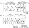
- FIG. 1 is a diagram schematically showing an example of the phase change of light that advances through two media.
- FIG. 1A shows a case in which the media 1 and 2 are both transparent
- FIG. 1B shows a case in which the medium 1 is transparent and the medium 2 is opaque.
- the phase change is continuous within the two media and at the boundary between the two media, as shown in FIG. 1A .
- the medium 2 is opaque
- a discontinuous phase difference is generated at the boundary between the media, as shown in FIG. 1B .
- the case in which the phase is delayed due to a discontinuous phase change is referred to as a negative phase change, as shown in FIG. 1B .
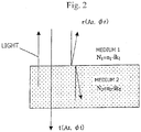
- the amplitude of the reflected light r at the boundary of the media 1 and 2 is A r > 0, and the phase is ⁇ r ;
- the amplitude of the transmitted light t at the boundary of the media 1 and 2 is A t > 0, and the phase is ⁇ t .
- the refractive index of the medium 1 is n 1
- the extinction coefficient of the medium is k 1
- the refractive index of the medium 2 is n 2
- the extinction coefficient of the medium is k 3 (*2).
- the reflected light r and transmitted light t are real numbers. Therefore, the following hold true based on Eqs. 4 and 5. Since the phases of the incident light and the transmitted light are the same, a discontinuous phase change does not occur at the boundary when light passes through the boundary of the media 1 and 2. However, the reflected light r and the transmitted light t are complex numbers when one of the two media 1 and 2 is an absorbing medium. Therefore, sin ⁇ t does not become 0, and a discontinuous phase change occurs at the boundary when light passes through the boundary of the media 1 and 2.
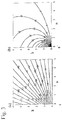
- FIG. 3A shows a case in which the refractive index n 1 and extinction coefficient k 1 of the medium 1 are set t be 1 and 0 (air or vacuum), respectively, and, based on Eq. 2, the phase change ⁇ t of the light that passes from the medium 1 to the medium 2 is calculated and the contour lines are plotted when the refractive index n 2 and the extinction coefficient k 2 of the medium 2 are varied (the horizontal axis represents the refractive index n, and the vertical axis represents the extinction coefficient k).
- FIG. 3B shows the phase change ⁇ t ' when light passes from the medium 2 to the medium 1 (the horizontal axis represents the refractive index n, and the vertical axis represents the extinction coefficient k).
- the medium 1 when the optically semitransmissive film has a single phase-difference reduction layer, the medium 1 can be made to correspond to a translucent substrate, and the medium 2 can be made to correspond to a phase-difference reduction layer.
- the extinction coefficient k at the exposure wavelength is substantially lower than the refractive index n and is close to 0. This results in a low value for the negative phase change at the boundary with the translucent substrate that corresponds to the medium 1, or a low positive phase change at the boundary with the atmosphere (air), and a continuous phase change such as that shown in FIG. 1A can be presumed to occur.
- an absorbing material in which the extinction coefficient k is considerable at about n ⁇ k, relative to the refractive index n, consideration must be given both to the discontinuous phase change at the boundary and to the conventional phase difference shown in Eqs. 1 and 3.
- phase ⁇ t ' corresponds to ⁇ '.
- the graph also shows (solid line) the relationship between the thickness d and the phase difference ⁇ n obtained from Eq. 1 for calculating the phase difference in a conventional single-layer phase-shift mask.
- the phase-difference reduction layer in the optically semitransmissive film of present embodiment comprises an absorbing film, i.e., an absorbing material in which the extinction coefficient k is relatively large. Therefore, a discontinuous negative phase change occurs at the boundary with the medium selected from the translucent substrate, another layer, or atmosphere adjacent to the phase-difference reduction layer, and the negative phase change sufficiently small to be ignored in conventional practice can be increased in the boundary between the substrate and the optically semitransmissive film. As a result, the phase difference ⁇ can be made less than the phase difference ⁇ 0 calculated using Eq.
- phase-difference reduction layer that has a phase difference ⁇ in the vicinity of 0°, e.g., a phase difference ⁇ that is 0 ⁇ 30°, while having a limited thickness (in practice, 1 nm or more, for example).
- an optically semitransmissive film phase-difference reduction layer
- phase difference ⁇ 0 having a negative value refers a case in which the phase difference is a negative value when expressed in the range of ⁇ 180°. In such a case, a phase difference of 360 degrees is expressed as 0 degrees.
- the thickness of the phase-difference reduction layer is not adjusted based on Eq. 1, but rather the relationship between the phase difference and the thickness as shown in FIG. 5 , for example, is calculated in advance using Eqs. 6 and 7; and the thickness is set so that a desired phase difference can be obtained.
- a zero point through which the phase change passes when changing from negative to positive can be selected as the phase difference, making it possible to obtain a phase-difference reduction layer in which the phase difference is exactly zero.
- the transmissivity can be adjusted by selecting a thickness that allows the phase difference to be adjusted in the ranges of 0 ⁇ 30°, 0 ⁇ 10°, 0 ⁇ 5°, and the like, based on the balance between the allowable phase difference and the transmissivity required in the phase-difference reduction layer.
- the transmissivity and phase difference of the optically semitransmissive film are suitably determined by design in accordance with the intended application of the optically semitransmissive film.
- a film material having a desired extinction coefficient k and a desired refractive index n can be selected so that the film thickness satisfies the required value of the transmissivity and the required value of the phase difference in accordance with the intended application.
- the film may be designed so that the transmissivity and phase difference are different than the transmissivity and phase difference that are originally required when the optically semitransmissive film is formed.
- the balance between the transmissivity variation and reflectivity variation that accompany washing, heat treatment, and other treatments of the optically semitransmissive film can be used to ensure that the transmissivity substantially does not vary even when washing, heat treatment, and other treatments are carried out, or to control the variation in the transmissivity caused by the aforementioned washing, heat treatment, and other treatments.
- phase difference ⁇ and the phase difference ⁇ 0 increases above 10 degrees or more, for example, the relationship between the film thickness and the phase difference ⁇ begins to form a broad curve, and the transmissivity, which varies depending on the film thickness, can be more easily adjusted.
- the phase-difference reduction layer is a single-layer optically semitransmissive film
- the phase difference and transmissivity of the optically semitransmissive film can be adjusted by adjusting the phase difference and transmissivity of the phase-difference reduction layer.
- the optically semitransmissive film is not limited to being provided with a single phase-difference reduction layer, but may be provided with two or more phase-difference reduction layers (same or different characteristics), or may be multilayered in combination with other layers.
- An example of a multilayered-optically semitransmissive film is an optically semitransmissive film having a multilayered structure comprising at least one phase-difference reduction layer in which the phase difference is negative and at least one layer in which the phase difference is positive, and in which the phase difference of the entire optically semitransmissive film is a desired phase difference wherein the negative phase difference and the positive phase difference cancel out each other.
- phase difference is positive because an antireflection film cannot ordinarily sufficiently demonstrate antireflective function if the material does not have a low extinction coefficient. Therefore, the phase difference in the phase-difference reduction layer is negative, and the phase difference of the antireflective layer having a positive phase difference cancel out each other, whereby the phase difference of the entire optically semitransmissive film can be adjusted to near zero.
- a relatively thin optically semitransmissive film can be obtained in accordance with the present embodiment.
- the phase-difference reduction layer preferably has a thickness selected from a range of 1 to 50 nm, and more preferably 1 to 30 nm.
- the thickness of the entire optically semitransmissive film is also preferably 1 to 50 nm, and more preferably 1 to 30 nm.
- the photomask blank of the present embodiment may, for example, be used for obtaining the photomask described in Patent Document 1.
- the photomask 1 described in Patent Document 1 is one in which a phase difference of 180° is provided to the aperture 3 disposed in the light-blocking portion (optically semitransmissive area) by cutting a translucent substrate 4 as a phase shifter, as shown in FIG. 6 , and in which the phase difference has been adjusted to 0 ⁇ 30° and the transmissivity has been adjusted to 15% or less by using the optically semitransmissive film 22 ( FIG. 7 ) of the present embodiment as the light-blocking portion 2. Therefore, the photomask 10 of the present embodiment has a structure in which the annular diaphragm 22 is disposed on the translucent substrate 4, as shown in FIG. 7 .
- the method shown in FIG. 8 is an example of a method for manufacturing the photomask.
- a resist film 11 is formed on a photomask blank 10, and a pattern is drawn on the resist film 11 using an electron beam or laser ( FIG. 8A ).
- the resist film 11 is developed, the optically semitransmissive film 22 is etched, and the translucent substrate 4 is etched down to a depth that produces a phase difference of 180° ( FIG. 8B ).
- the resist film 11 is subsequently peeled away ( FIG. 8C ).
- a resist film 12 is coated over the entire surface, and a pattern is drawn using electron beam lithography ( FIG. 8D ).
- the resist film 12 is subsequently developed, and the optically semitransmissive film 22 is etched ( FIG. 8E ).
- the resist film 12 is peeled away ( FIG. 8F ) to obtain a photomask 1 having a light-blocking portion 2 (optically semitransmissive area).
- the photomask 1 of the present embodiment can be used as a photomask having a light-blocking band.
- the light-blocking band is a light-blocking film composed of a chromium-based material, for example, formed on at least the peripheral portion of the pattern region, and is provided to prevent the occurrence of transfer pattern defects produced by transmitted light in the peripheral portion of the pattern region during photomask use.
- FIG. 9 is a diagram showing an example of the steps for manufacturing the photomask having a light-blocking band.
- a light-blocking film 13 is formed on the photomask blank 10 shown in FIG. 7 , a resist film 11 is formed on the light-blocking film, and a pattern is drawn using an electron beam or a laser ( FIG. 9A ).
- the resist film 11 is developed, the light-blocking film 13 is etched, the optically semitransmissive film 22 is etched, and the translucent substrate 4 is etched down to a depth that produces a phase difference of 180° ( FIG. 9B ).
- the resist film 11 is subsequently peeled away ( FIG. 9C ).
- a resist film 12 is coated over the entire surface ( FIG. 9D ), and a pattern is drawn using electron beam lithography.
- the resist film 12 is subsequently developed, the light-blocking film 13 is etched, and the optically semitransmissive film 22 is etched ( FIG. 9E ).
- the resist film 12 is removed ( FIG. 9F ), a resist film 14 is again coated over the entire surface ( FIG. 9G ), a resist pattern is formed to leave only a region in which the light-blocking band is formed ( FIG. 9h ), the chromium in the transfer region I is thereafter etched ( FIG. 9i ), and the remaining resist film 14 is peeled away ( FIG. 9h ) to obtain a photomask 15 having a light-blocking band 33 ( FIG. 9j ).
- the pattern arrangement on the photomask 1 and the manufacturing steps described above are imposed by the pattern arrangement on the photomask 1 and the manufacturing steps described above.
- the manufacturing steps for example, rather than etching down the translucent substrate 4 and thereafter forming a light-blocking portion 2 composed of an optically semitransmissive film 22 as described above, the light-blocking portion 2 composed of the optically semitransmissive film 22 may be formed and the translucent substrate 4 etched thereafter.
- the phase shifter formed in the aperture 3 may be a film that causes phase shifting.
- the photomask blank 10 would be one in which a phase-shifting film is disposed on the optically semitransmissive film 22 or between the translucent substrate 4 and the optically semitransmissive film 22.
- the optically semitransmissive film 22 may comprise a single-layer film or a film having two or more layers. In the case of two or more layers, at least one of the layers can be a phase-difference reduction layer that produces a negative phase change at the boundary.
- an antireflective layer can be disposed on the phase-difference reduction layer. In other words, the phase difference is usually positive because the antireflective film is incapable of adequately demonstrating an antireflective function if it is not made of a material having a low extinction coefficient.
- the phase difference in the phase-difference reduction layer is set to be negative so as to cancel out the phase difference of the antireflective film, which has a positive phase difference, whereby an antireflective function can be provided and the phase difference of the entire optically semitransmissive film can be adjusted to near zero.
- the antireflective film may be disposed on the phase-difference reduction layer (the side on which the surface of the photomask blank is present) when lower surface reflectivity is desired in the photomask blank.
- the antireflective film may be disposed below the phase-difference reduction layer (between the translucent substrate and the phase-difference reduction layer) when lower reflectivity is desired in the reverse surface, and the antireflective film may be disposed on both sides of the phase-difference reduction layer when lower reflectivity is desired in both the surface and the reverse side.
- the reflectivity is adjusted by designing the film so as to obtain a reflectivity that is equal to or less than the allowable value at the desired wavelength in the desired surface within a range in which adjustment can be made with consideration given to the phase difference and transmissivity in the case of a single layer or multiple layers.
- the optically semitransmissive film 22 may be a film that has been heat-treated at about 150 to 500°C, for example, or more preferably about 250 to 500°C; treated by UV or laser radiation; or treated in another manner in order to prevent variability in the characteristics due heat processing or other processing after film formation, or to prevent variability in the optical properties caused by washing or another chemical treatment.
- the optical characteristics must be matched to the exposure wavelength of the exposure device in which the photomask 1 is to be used.
- the exposure wavelength of the photomask 1 is preferably one in which consideration is given to exposure wavelengths in the range of 150 nm to 250 nm, which includes KrF excimer laser light (wavelength: 248 nm), ArF excimer laser light (wavelength: 193 nm), and F 2 excimer laser light (wavelength: 157 nm).
- an exposure wavelength in which consideration is given to exposure wavelengths in the range of 150 nm to 200 nm, which includes ArF excimer laser light (wavelength: 193 nm) and F 2 excimer laser light (wavelength: 157 nm). These are next-generation exposure wavelengths.
- the reflectivity of the surface (the film surface side) of the photomask blank is preferably kept to 30% or less at the exposure wavelength. The reflectivity is also preferably kept to 30% or less on the reverse side of the photomask blank. The reflectivity is preferably kept to about 40% or less at the scanning wavelength of the photomask 1 and photomask blank 10. Examples of scanning wavelengths include 257 nm, 266 nm, 364 nm, 488 nm, and 633 nm.
- An optically semitransmissive film provided with a single phase-difference reduction layer composed of chromium nitride was formed on a translucent substrate composed of synthetic quartz glass to obtain a photomask blank having the structure shown in FIG. 7 .
- an optically semitransmissive film was formed by sputtering a chromium target onto a translucent substrate in an atmosphere of argon and nitrogen.
- the table in FIG. 10 shows the transmissivity and phase difference of an optically semitransmissive film at an ArF excimer laser wavelength of 193 nm, which is the exposure wavelength maintained when a photomask is used.
- the transmissivity was measured using a spectrophotometer, and the phase difference was measured using a phase difference measuring device (MPM-193, manufactured by Lasertec). In the present example, the transmissivity was kept within a range of 5 to 15%.
- the transmissivity was kept within a range of 5 to 15% while keeping the phase difference near zero by using a relatively thin film.
- An optically semitransmissive film provided with a single phase-difference reduction layer composed of tantalum hafnium was formed on a translucent substrate composed of synthetic quartz glass to obtain the photomask blank shown in FIG. 7 .
- the table in FIG. 10 shows the results of measuring the transmissivity and phase difference of an optically semitransmissive film at an ArF excimer laser wavelength of 193 nm, which is the exposure wavelength maintained when a photomask is used.
- the same measuring means as used in example 1 were employed.
- the transmissivity was kept within a range of 5 to 15%.
- the transmissivity was kept within a range of 5 to 15% while keeping the phase difference near zero by using a relatively thin film.
- An optically semitransmissive film provided with a single phase-difference reduction layer composed of silicon was formed on a translucent substrate composed of synthetic quartz glass to obtain a photomask blank shown in FIG. 7 .
- an optically semitransmissive film was formed by sputtering a silicon target onto a translucent substrate in an argon atmosphere.
- the table in FIG. 10 shows the results of measuring the transmissivity and phase difference of an optically semitransmissive film at an ArF excimer laser wavelength of 193 nm of, which is the exposure wavelength maintained when a photomask is used.
- the same measuring means as used in example 1 were employed.
- the transmissivity was kept within a range of 5 to 15%.
- the transmissivity was kept within a range of 5 to 15% while keeping the phase difference near zero by using a relatively thin film.
- An optically semitransmissive film having a MoSiN film as the optically semitransmissive portion was formed on a conventional halftone phase-shift mask on a translucent substrate composed of synthetic quartz glass to obtain the photomask blank shown in FIG. 7 .
- a MoSiN film does not have a thickness region in which the phase difference is 0° or less in a region below the minimal thickness at which the phase difference is 180°. Therefore, in comparative example 1, the phase difference was kept very small in a region of relatively small film thicknesses, but the transmissivity was still excessively high. In comparative example 2, the thickness was adjusted to give the phase difference a zero limit. However, the optically semitransmissive portion was very thick at 100 nm or more, and the film was not suitable for micropatterning.
- the optically semitransmissive film Cr-N of example 1 was dry etched using Cl 2 +O 2 as etching gas, the TaHf of example 2 was dry etched using Cl 2 gas, and the Si of example 3 was dry etched using CF 4 gas.
- the translucent substrate was dry etched using CF4 + O 2 as etching gas. The translucent substrate had sufficient resistance to the etching of the optically semitransmissive film.
- the present examples involve manufacturing photomasks having a light-blocking band by using the photomask blanks of examples 2 and 3.
- the photomasks were formed in accordance with the steps in FIG. 9 by using the photomask blanks of examples 2 and 3.
- a chromium-based film was used as the light-blocking film for the light-blocking band, and the film was dry etched using Cl 4 + O 2 as etching gas.
- the etching of examples 2 and 3 was carried out in the same manner as in examples 5 and 6. Selective etching was possible because the optically semitransmissive film and light-blocking film both had good etching selectivity, and a good pattern shape was obtained with low dimensional error by etching the optically semitransmissive film using the light-blocking film as a mask.
- the same chromium material as that of the light-blocking material for the light-blocking band was used as the optically semitransmissive film material, and it was therefore difficult to selectively etch the photomask blank of example 1.
- a phase-difference reduction layer 16 composed of molybdenum and silicon, and an antireflective layer 17 composed of molybdenum, silicon, and nitrogen were layered on a translucent substrate 4 composed of synthetic quartz glass to form an optically semitransmissive film 22, as shown in FIG. 11 , and a photomask blank 18 was obtained.
- the table in FIG. 12 shows the film characteristics of the examples 9 to 11.
- the refractive index, extinction coefficient, transmissivity, reflectivity, and phase difference are the values observed at an ArF excimer laser wavelength of 193 nm, which is the exposure wavelength maintained when a photomask is used.
- the transmissivity and reflectivity were measured using a spectrophotometer, and the phase difference was measured using a phase difference measuring device (MPM-193, manufactured by Lasertec). In the present example, the transmissivity was kept within a range of 5 to 15%.
- FIG. 13 shows the relationship between the film thickness and the phase difference in the material of the antireflective layer used in examples 9 to 11. It is apparent from the diagram that the phase difference of the optically semitransmissive film can be adjusted to be a negative value by layering an antireflective layer on the phase-difference reduction layer.
- FIG. 14 is a diagram showing the reflection spectrum of the surface of the photomask blank used in examples 9 to 11.
- the transmissivity was kept within a range of 5 to 15% while keeping the phase difference near zero by using a relatively thin film, as shown in FIG. 12 .
- the reflectivity at the exposure wavelength was a relatively low value of 30% or less, and in example 11, the reflectivity was kept to 40% or less at 266 nm, which is the photomask scanning wavelength, as shown in FIG. 14 .
- an MoSiN antireflective layer was formed using a target composed of molybdenum and silicon as a sputtering target, but a silicon target may be used to obtain a SiN antireflective layer.
- Oxygen may furthermore be added to the film formation atmosphere to form an antireflective layer composed of MoSiO, SiO, MoSiON, SiON, and the like.
- the molybdenum content of the antireflective layer and/or the phase-difference reduction layer is preferably less than 30%.
- the molybdenum and silicon ratio in the sputtering target is preferably set in a range of 0:100 to 30:70.
- a photomask blank was fabricated using only a phase-difference reduction layer, without the use of an antireflective film (see the table in FIG. 12 ). As a result, the phase difference was kept to ⁇ 30° and the transmissivity was kept within a range of 5 to 15%, but the reflectivity was a very high value.
- a film composed of a material in which the refractive index n was greater than the extinction coefficient k was formed as the phase-difference reduction layer, and an antireflective layer was formed on the phase-difference reduction layer (see the table in FIG. 12 ) .
- the transmissivity was kept within a range of 5 to 15% and the reflectivity was reduced, but the film had a very considerable phase difference.
- the transmissivity was designed to be kept within a range of 5 to 15%, but the design value of the transmissivity can be varied in accordance with the design of the transfer pattern when the photomask is being used.
- the design value of the transmissivity can be selected from a range that is 40% or less, for example.
- the material of the phase-difference reduction layer is furthermore not limited to the aforementioned materials, and the material may be one in which a negative phase change is produced by the transmission and/or reflection of exposure light at the boundary with the atmosphere to which the optically semitransmissive film is exposed, and/or at the boundary between the optically semitransmissive film and the translucent substrate.
- the material of the phase-difference reduction layer may contain one or more materials selected from Ta, Hf, Si, Cr, Ag, Au, Cu, Al, Mo, and other materials.
- the material of the optically semitransmissive film preferably has a phase difference-reducing effect in the UV region, is resistant to alkali washing fluids and acid washing fluids, and has excellent patterning characteristics. Based on these points, it is preferable to use a material containing silicon alone or both silicon and a metal (Mo, Ta, W, Cr, Zr, Hf, or another metal). From the standpoint of photomask production, the material of the optically semitransmissive film preferably has a high etching selectivity ratio in relation to the chromium light-blocking film as a light-blocking band. For example, the dimensional precision of the translucent substrate portion can be improved by including a material that prevents the optically semitransmissive film from being etched during etching of a translucent substrate.
- optically semitransmissive film that has, e.g., a multilayered structure comprising a phase-difference reduction layer and an antireflective layer
- configuring these layers from a material that can be etched using the same etching medium is preferred from the standpoint of simplifying the mask manufacturing steps when the film is patterned.
Landscapes
- Physics & Mathematics (AREA)
- General Physics & Mathematics (AREA)
- Preparing Plates And Mask In Photomechanical Process (AREA)
Claims (12)
- Fotomaskenrohling (18) zur Herstellung einer Fotomaske (1) mit einem Maskenmuster auf einem transparentem Substrat (4), umfassend einen Film (22), der wenigstens zwei Schichten aus einer ersten Schicht (16) mit einer Phasendifferenz Δθ1 und einer zweiten Schicht mit einer Phasendifferenz Δθ2 enthält, wobei der Film auf dem transparenten Substrat (4) gebildet ist, wobei die Phasendifferenz Δθ1 die Phasendifferenz zwischen einer Phase eines Lichts, das durch die erste Schicht (16) hindurch transmittiert wird, und einer Phase eines Lichts ist, das durch eine Schicht von Luft mit der gleichen Dicke wie die erste Schicht (16) hindurch transmittiert wird,
wobei die Phasendifferenz Δθ2 die Phasendifferenz zwischen einer Phase eines Lichts, das durch die zweite Schicht (17) hindurch transmittiert wird, und einer Phase eines Lichts ist, das durch eine Schicht von Luft mit der gleichen Dicke wie die zweite Schicht (17) hindurch transmittiert wird,
wobei die Phasendifferenz des Films (22), der wenigstens die zwei Schichten (16, 17) enthält, in einem Bereich von -30° bis +30° ist,
wobei die erste Schicht (16) ein Material umfasst, das Molybdän (Mo) und Silicium (Si) enthält,
dadurch gekennzeichnet, dass der Molybdängehalt der ersten Schicht (16) weniger als 30 at % ist, und die zweite Schicht (17) eine Antireflexionsschicht ist. - Fotomaskenrohling (18) nach Anspruch 1, wobei die erste Schicht (16) unter Verwendung eines Sputtertargets gebildet ist, bei dem ein Verhältnis von Mo zu Si in einem Bereich von 0:100 bis 30:70 eingestellt ist.
- Fotomaskenrohling (18) nach Anspruch 1 oder 2, wobei die erste Schicht (16) ein Material umfasst, das einen Ausdruck k1 ≥ n1 erfüllt, wobei n1 ein Brechungsindex ist, und k1 ein Extinktionskoeffizient ist.
- Fotomaskenrohling (18) nach Anspruch 3, wobei der Extinktionskoeffizient k1 der ersten Schicht (16) k1 ≥ 1.5 erfüllt.
- Fotomaskenrohling (18) nach Anspruch 3, wobei der Extinktionskoeffizient k1 der ersten Schicht (16) k1 ≥ 2.0 erfüllt.
- Fotomaskenrohling (18) nach Anspruch 3, wobei der Extinktionskoeffizient k1 der ersten Schicht (16) k1 ≥ 2.5 erfüllt.
- Fotomaskenrohling (18) nach einem der Ansprüche 1 bis 6, wobei die zweite Schicht (17) MoSiN, MoSiO, MoSiON, SiN, SiO oder SiON umfasst.
- Fotomaskenrohling (18) nach Anspruch 7, wobei der Molybdängehalt der zweiten Schicht (17) kleiner als 30 at % ist.
- Fotomaskenrohling (18) nach Anspruch 7 oder 8, wobei die zweite Schicht (17) unter Verwendung eines Sputtertargets gebildet ist, bei dem ein Verhältnis von Mo zu Si in einem Bereich von 0:100 bis 30:70 eingestellt ist.
- Fotomaskenrohling (18) nach einem der Ansprüche 1 bis 9, wobei die Antireflexionsschicht (17) auf der ersten Schicht (16) gebildet ist.
- Fotomaskenrohling (18) nach einem der Ansprüche 1 bis 10, wobei eine Dicke des Films (22), der wenigstens die zwei Schichten (16, 17) enthält, in einem Bereich von 1 bis 50 nm ist.
- Fotomaske (1), hergestellt unter Verwendung des Fotomaskenrohlings (18) nach einem der Ansprüche 1-11.
Applications Claiming Priority (4)
| Application Number | Priority Date | Filing Date | Title |
|---|---|---|---|
| JP2004178895 | 2004-06-16 | ||
| JP2005137171 | 2005-05-10 | ||
| PCT/JP2005/010713 WO2005124454A1 (ja) | 2004-06-16 | 2005-06-10 | 光半透過膜、フォトマスクブランク及びフォトマスク、並びに光半透過膜の設計方法 |
| EP05749063.3A EP1783546B1 (de) | 2004-06-16 | 2005-06-10 | Halbdurchlässiger film, fotomaskenrohling und fotomaske |
Related Parent Applications (3)
| Application Number | Title | Priority Date | Filing Date |
|---|---|---|---|
| EP05749063.3 Division | 2005-06-10 | ||
| EP05749063.3A Division-Into EP1783546B1 (de) | 2004-06-16 | 2005-06-10 | Halbdurchlässiger film, fotomaskenrohling und fotomaske |
| EP05749063.3A Division EP1783546B1 (de) | 2004-06-16 | 2005-06-10 | Halbdurchlässiger film, fotomaskenrohling und fotomaske |
Publications (3)
| Publication Number | Publication Date |
|---|---|
| EP2657768A2 EP2657768A2 (de) | 2013-10-30 |
| EP2657768A3 EP2657768A3 (de) | 2014-01-08 |
| EP2657768B1 true EP2657768B1 (de) | 2020-08-05 |
Family
ID=35509857
Family Applications (2)
| Application Number | Title | Priority Date | Filing Date |
|---|---|---|---|
| EP05749063.3A Expired - Fee Related EP1783546B1 (de) | 2004-06-16 | 2005-06-10 | Halbdurchlässiger film, fotomaskenrohling und fotomaske |
| EP13176446.6A Expired - Fee Related EP2657768B1 (de) | 2004-06-16 | 2005-06-10 | Photomaskenrohling und Photomaske |
Family Applications Before (1)
| Application Number | Title | Priority Date | Filing Date |
|---|---|---|---|
| EP05749063.3A Expired - Fee Related EP1783546B1 (de) | 2004-06-16 | 2005-06-10 | Halbdurchlässiger film, fotomaskenrohling und fotomaske |
Country Status (6)
| Country | Link |
|---|---|
| US (5) | US7651823B2 (de) |
| EP (2) | EP1783546B1 (de) |
| JP (2) | JP4330622B2 (de) |
| KR (4) | KR101004395B1 (de) |
| TW (1) | TWI282483B (de) |
| WO (1) | WO2005124454A1 (de) |
Families Citing this family (25)
| Publication number | Priority date | Publication date | Assignee | Title |
|---|---|---|---|---|
| US7651823B2 (en) * | 2004-06-16 | 2010-01-26 | Hoya Corporation | Optically semitransmissive film, photomask blank and photomask, and method for designing optically semitransmissive film |
| JP5165833B2 (ja) * | 2005-02-04 | 2013-03-21 | 信越化学工業株式会社 | フォトマスクブランク、フォトマスク、およびフォトマスクブランクの製造方法 |
| JP2007271661A (ja) * | 2006-03-30 | 2007-10-18 | Hoya Corp | マスクブランク及びハーフトーン型位相シフトマスク |
| JP5023589B2 (ja) * | 2006-07-21 | 2012-09-12 | 大日本印刷株式会社 | フォトマスクおよび該フォトマスクの設計方法 |
| JP4528803B2 (ja) * | 2007-06-15 | 2010-08-25 | 信越化学工業株式会社 | ハーフトーン型位相シフトマスク |
| JP2008310091A (ja) * | 2007-06-15 | 2008-12-25 | Shin Etsu Chem Co Ltd | ハーフトーン型位相シフトマスク |
| JP5702920B2 (ja) * | 2008-06-25 | 2015-04-15 | Hoya株式会社 | 位相シフトマスクブランク、位相シフトマスクおよび位相シフトマスクブランクの製造方法 |
| JP5615488B2 (ja) * | 2008-06-30 | 2014-10-29 | Hoya株式会社 | 位相シフトマスクの製造方法 |
| KR101295235B1 (ko) * | 2008-08-15 | 2013-08-12 | 신에쓰 가가꾸 고교 가부시끼가이샤 | 그레이톤 마스크 블랭크, 그레이톤 마스크, 및 제품 가공 표지 또는 제품 정보 표지의 형성방법 |
| JP4831368B2 (ja) * | 2008-08-15 | 2011-12-07 | 信越化学工業株式会社 | グレートーンマスクブランク及びグレートーンマスク |
| JP4849276B2 (ja) * | 2008-08-15 | 2012-01-11 | 信越化学工業株式会社 | グレートーンマスクブランク、グレートーンマスク、及び製品加工標識又は製品情報標識の形成方法 |
| KR20160138586A (ko) * | 2008-09-30 | 2016-12-05 | 호야 가부시키가이샤 | 포토마스크 블랭크, 포토마스크 및 그 제조 방법과, 반도체 디바이스의 제조 방법 |
| WO2010050447A1 (ja) * | 2008-10-29 | 2010-05-06 | Hoya株式会社 | フォトマスクブランク、フォトマスク及びその製造方法 |
| TWI461833B (zh) * | 2010-03-15 | 2014-11-21 | Hoya Corp | 多調式光罩、多調式光罩之製造方法及圖案轉印方法 |
| JP5154626B2 (ja) | 2010-09-30 | 2013-02-27 | Hoya株式会社 | マスクブランク、転写用マスク、転写用マスクの製造方法、および半導体デバイスの製造方法 |
| JP6058318B2 (ja) | 2011-09-14 | 2017-01-11 | Hoya株式会社 | マスクブランク、転写用マスク、転写用マスクの製造方法、および半導体デバイスの製造方法 |
| JP5474129B2 (ja) * | 2012-05-24 | 2014-04-16 | 信越化学工業株式会社 | 半透明積層膜の設計方法およびフォトマスクブランクの製造方法 |
| JP6420958B2 (ja) * | 2014-03-04 | 2018-11-07 | Hoya株式会社 | インプリント用モールドブランクおよびインプリント用モールド |
| JP5976970B1 (ja) * | 2015-02-24 | 2016-08-24 | 日東電工株式会社 | 光透過性フィルム |
| JP6380204B2 (ja) * | 2015-03-31 | 2018-08-29 | 信越化学工業株式会社 | ハーフトーン位相シフトマスクブランク、ハーフトーン位相シフトマスク及びパターン露光方法 |
| JP6087401B2 (ja) * | 2015-08-14 | 2017-03-01 | Hoya株式会社 | マスクブランク、位相シフトマスクおよび半導体デバイスの製造方法 |
| CN114675486A (zh) * | 2016-08-26 | 2022-06-28 | Hoya株式会社 | 掩模坯料、转印用掩模及半导体器件的制造方法 |
| TW201823855A (zh) * | 2016-09-21 | 2018-07-01 | 日商Hoya股份有限公司 | 光罩之製造方法、光罩、及顯示裝置之製造方法 |
| JP7037919B2 (ja) * | 2017-11-14 | 2022-03-17 | アルバック成膜株式会社 | マスクブランク、ハーフトーンマスクおよびその製造方法 |
| JP2023050611A (ja) * | 2021-09-30 | 2023-04-11 | 株式会社エスケーエレクトロニクス | フォトマスク及びフォトマスクの製造方法 |
Family Cites Families (23)
| Publication number | Priority date | Publication date | Assignee | Title |
|---|---|---|---|---|
| JPH0695363A (ja) * | 1992-09-11 | 1994-04-08 | Toppan Printing Co Ltd | フォトマスクブランク及びその製造方法並びにフォトマスク |
| JP3229446B2 (ja) * | 1993-07-13 | 2001-11-19 | 大日本印刷株式会社 | ハーフトーン位相シフトフォトマスク及びハーフトーン位相シフトフォトマスク用ブランクス |
| KR100295385B1 (ko) | 1993-04-09 | 2001-09-17 | 기타지마 요시토시 | 하프톤위상쉬프트포토마스크,하프톤위상쉬프트포토마스크용블랭크스및이들의제조방법 |
| US5629115A (en) | 1993-04-30 | 1997-05-13 | Kabushiki Kaisha Toshiba | Exposure mask and method and apparatus for manufacturing the same |
| JP3222678B2 (ja) | 1994-02-25 | 2001-10-29 | 株式会社東芝 | 半透明膜の設計方法 |
| JPH08202016A (ja) * | 1995-01-20 | 1996-08-09 | Sony Corp | ハーフトーン型位相シフトマスク及びレジスト露光方法 |
| US5660955A (en) * | 1995-11-15 | 1997-08-26 | Lg Semkon Co., Ltd. | Phase shift mask and manufacturing method thereof |
| JPH10198017A (ja) * | 1997-01-10 | 1998-07-31 | Toppan Printing Co Ltd | 位相シフトフォトマスク及び位相シフトフォトマスク用ブランク |
| JPH1126355A (ja) | 1997-07-07 | 1999-01-29 | Toshiba Corp | 露光用マスク及びその製造方法 |
| JP2000181048A (ja) * | 1998-12-16 | 2000-06-30 | Sharp Corp | フォトマスクおよびその製造方法、並びにそれを用いた露光方法 |
| JP4328922B2 (ja) | 1999-09-21 | 2009-09-09 | 信越化学工業株式会社 | 位相シフト型フォトマスク |
| US7385106B2 (en) | 2000-01-24 | 2008-06-10 | Ramot At Tel Aviv University Ltd. | Plants tolerant of environmental stress conditions, methods of generating same and novel polynucleotide sequence utilized thereby |
| JP4686006B2 (ja) * | 2000-04-27 | 2011-05-18 | 大日本印刷株式会社 | ハーフトーン位相シフトフォトマスクとハーフトーン位相シフトフォトマスク用ブランクス、及びハーフトーン位相シフトフォトマスクの製造方法 |
| KR100618811B1 (ko) | 2001-03-20 | 2006-08-31 | 삼성전자주식회사 | 반도체 소자 제조를 위한 위상 반전 마스크 및 그 제조방법 |
| JP3708877B2 (ja) | 2001-05-01 | 2005-10-19 | 松下電器産業株式会社 | フォトマスク |
| JP2003050454A (ja) | 2001-08-07 | 2003-02-21 | Canon Inc | 位相シフトマスク及びその製造方法 |
| DE10307518B4 (de) * | 2002-02-22 | 2011-04-14 | Hoya Corp. | Halbtonphasenschiebermaskenrohling, Halbtonphasenschiebermaske und Verfahren zu deren Herstellung |
| DE10307545A1 (de) * | 2002-02-22 | 2003-11-06 | Hoya Corp | Zuschnitt für halbtonartige Phasenverschiebungsmaske und zugehörige Phasenverschiebungsmaske |
| JP2003322947A (ja) * | 2002-04-26 | 2003-11-14 | Hoya Corp | ハーフトーン型位相シフトマスクブランク及びハーフトーン型位相シフトマスク |
| JP4290386B2 (ja) * | 2002-04-26 | 2009-07-01 | Hoya株式会社 | ハーフトーン型位相シフトマスクブランク及びハーフトーン型位相シフトマスク |
| JP3727318B2 (ja) * | 2002-04-30 | 2005-12-14 | 松下電器産業株式会社 | フォトマスク及びその作成方法 |
| JP2004085760A (ja) * | 2002-08-26 | 2004-03-18 | Toppan Printing Co Ltd | ハーフトーン型位相シフトマスク用ブランク及びそれを用いたハーフトーン型位相シフトマスク、並びにパターン転写法 |
| US7651823B2 (en) * | 2004-06-16 | 2010-01-26 | Hoya Corporation | Optically semitransmissive film, photomask blank and photomask, and method for designing optically semitransmissive film |
-
2005
- 2005-06-10 US US11/629,210 patent/US7651823B2/en active Active
- 2005-06-10 WO PCT/JP2005/010713 patent/WO2005124454A1/ja active Application Filing
- 2005-06-10 EP EP05749063.3A patent/EP1783546B1/de not_active Expired - Fee Related
- 2005-06-10 KR KR1020087027358A patent/KR101004395B1/ko active IP Right Grant
- 2005-06-10 JP JP2006514723A patent/JP4330622B2/ja active Active
- 2005-06-10 KR KR1020097013134A patent/KR101052654B1/ko active IP Right Grant
- 2005-06-10 EP EP13176446.6A patent/EP2657768B1/de not_active Expired - Fee Related
- 2005-06-10 KR KR1020077000696A patent/KR100967995B1/ko active IP Right Grant
- 2005-06-10 KR KR1020117005535A patent/KR101149123B1/ko active IP Right Grant
- 2005-06-16 TW TW094119962A patent/TWI282483B/zh active
-
2008
- 2008-12-15 JP JP2008318999A patent/JP4507216B2/ja active Active
-
2009
- 2009-12-07 US US12/632,103 patent/US7955762B2/en active Active
-
2011
- 2011-04-29 US US13/098,096 patent/US8110323B2/en active Active
- 2011-12-29 US US13/340,228 patent/US8486588B2/en active Active
-
2013
- 2013-06-13 US US13/917,338 patent/US8580466B1/en active Active
Non-Patent Citations (1)
| Title |
|---|
| None * |
Also Published As
| Publication number | Publication date |
|---|---|
| EP1783546B1 (de) | 2014-03-05 |
| TWI282483B (en) | 2007-06-11 |
| US20130011772A1 (en) | 2013-01-10 |
| WO2005124454A1 (ja) | 2005-12-29 |
| US20110207032A1 (en) | 2011-08-25 |
| EP2657768A3 (de) | 2014-01-08 |
| JP2009086681A (ja) | 2009-04-23 |
| EP1783546A4 (de) | 2013-01-09 |
| EP1783546A1 (de) | 2007-05-09 |
| TW200606577A (en) | 2006-02-16 |
| JPWO2005124454A1 (ja) | 2008-04-17 |
| KR101149123B1 (ko) | 2012-05-25 |
| KR100967995B1 (ko) | 2010-07-07 |
| US7955762B2 (en) | 2011-06-07 |
| US8580466B1 (en) | 2013-11-12 |
| US20130309602A1 (en) | 2013-11-21 |
| US7651823B2 (en) | 2010-01-26 |
| KR20110043745A (ko) | 2011-04-27 |
| KR101052654B1 (ko) | 2011-07-28 |
| US8486588B2 (en) | 2013-07-16 |
| US8110323B2 (en) | 2012-02-07 |
| US20070269723A1 (en) | 2007-11-22 |
| EP2657768A2 (de) | 2013-10-30 |
| JP4330622B2 (ja) | 2009-09-16 |
| KR20080111119A (ko) | 2008-12-22 |
| US20100159368A1 (en) | 2010-06-24 |
| KR20090084957A (ko) | 2009-08-05 |
| KR101004395B1 (ko) | 2010-12-28 |
| KR20070022148A (ko) | 2007-02-23 |
| JP4507216B2 (ja) | 2010-07-21 |
Similar Documents
| Publication | Publication Date | Title |
|---|---|---|
| EP2657768B1 (de) | Photomaskenrohling und Photomaske | |
| KR100213151B1 (ko) | 감쇠하는 상 이동 마스크의 제조를 위한 박막의 물질 | |
| JP3645882B2 (ja) | ハーフトーン型位相シフトマスクブランクの製造方法 | |
| JP2000181049A (ja) | ハーフトーン型位相シフトマスクブランク及びハーフトーン型位相シフトマスク | |
| WO2007074806A1 (ja) | フォトマスクブランク及びフォトマスクの製造方法、並びに半導体装置の製造方法 | |
| US7169513B2 (en) | Halftone type phase shift mask blank and phase shift mask thereof | |
| JP7095157B2 (ja) | 位相シフトマスクブランクおよびこれを用いた位相シフトマスクの製造方法、並びに表示装置の製造方法 | |
| US6132908A (en) | Photo mask and exposure method using the same | |
| JPH10186632A (ja) | ハーフトーン型位相シフトマスク用ブランク及びハーフトーン型位相シフトマスク | |
| KR20080110467A (ko) | 하프톤형 위상 시프트 마스크 | |
| JP3641460B2 (ja) | ハーフトーン型位相シフトマスクブランク及びハーフトーン型位相シフトマスク | |
| JP2004004791A (ja) | ハーフトーン型位相シフトマスクブランク及びハーフトーン型位相シフトマスク | |
| JP4951813B2 (ja) | ハーフトーン型位相シフトマスク用ブランク | |
| JP4459523B2 (ja) | ハーフトーン型位相シフトマスクブランク及びハーフトーン型位相シフトマスク | |
| JP2020042208A (ja) | マスクブランク、転写用マスクおよび半導体デバイスの製造方法 | |
| JP4528803B2 (ja) | ハーフトーン型位相シフトマスク | |
| JP2003005349A (ja) | ハーフトーン型位相シフトマスク用ブランクおよびハーフトーン型位相シフトマスク |
Legal Events
| Date | Code | Title | Description |
|---|---|---|---|
| PUAI | Public reference made under article 153(3) epc to a published international application that has entered the european phase |
Free format text: ORIGINAL CODE: 0009012 |
|
| AC | Divisional application: reference to earlier application |
Ref document number: 1783546 Country of ref document: EP Kind code of ref document: P |
|
| AK | Designated contracting states |
Kind code of ref document: A2 Designated state(s): DE |
|
| PUAL | Search report despatched |
Free format text: ORIGINAL CODE: 0009013 |
|
| AK | Designated contracting states |
Kind code of ref document: A3 Designated state(s): DE |
|
| RIC1 | Information provided on ipc code assigned before grant |
Ipc: G03F 1/26 20120101ALN20131203BHEP Ipc: H01L 21/027 20060101ALI20131203BHEP Ipc: G03F 1/32 20120101ALN20131203BHEP Ipc: G03F 1/34 20120101ALN20131203BHEP Ipc: G03F 1/54 20120101ALN20131203BHEP Ipc: G03F 7/20 20060101AFI20131203BHEP |
|
| 17P | Request for examination filed |
Effective date: 20140708 |
|
| RBV | Designated contracting states (corrected) |
Designated state(s): DE |
|
| RAP1 | Party data changed (applicant data changed or rights of an application transferred) |
Owner name: HOYA CORPORATION |
|
| GRAJ | Information related to disapproval of communication of intention to grant by the applicant or resumption of examination proceedings by the epo deleted |
Free format text: ORIGINAL CODE: EPIDOSDIGR1 |
|
| GRAP | Despatch of communication of intention to grant a patent |
Free format text: ORIGINAL CODE: EPIDOSNIGR1 |
|
| STAA | Information on the status of an ep patent application or granted ep patent |
Free format text: STATUS: REQUEST FOR EXAMINATION WAS MADE |
|
| GRAP | Despatch of communication of intention to grant a patent |
Free format text: ORIGINAL CODE: EPIDOSNIGR1 |
|
| STAA | Information on the status of an ep patent application or granted ep patent |
Free format text: STATUS: GRANT OF PATENT IS INTENDED |
|
| INTG | Intention to grant announced |
Effective date: 20200401 |
|
| GRAS | Grant fee paid |
Free format text: ORIGINAL CODE: EPIDOSNIGR3 |
|
| GRAA | (expected) grant |
Free format text: ORIGINAL CODE: 0009210 |
|
| STAA | Information on the status of an ep patent application or granted ep patent |
Free format text: STATUS: THE PATENT HAS BEEN GRANTED |
|
| AC | Divisional application: reference to earlier application |
Ref document number: 1783546 Country of ref document: EP Kind code of ref document: P |
|
| AK | Designated contracting states |
Kind code of ref document: B1 Designated state(s): DE |
|
| REG | Reference to a national code |
Ref country code: DE Ref legal event code: R096 Ref document number: 602005056945 Country of ref document: DE |
|
| REG | Reference to a national code |
Ref country code: DE Ref legal event code: R097 Ref document number: 602005056945 Country of ref document: DE |
|
| PLBE | No opposition filed within time limit |
Free format text: ORIGINAL CODE: 0009261 |
|
| STAA | Information on the status of an ep patent application or granted ep patent |
Free format text: STATUS: NO OPPOSITION FILED WITHIN TIME LIMIT |
|
| 26N | No opposition filed |
Effective date: 20210507 |
|
| PGFP | Annual fee paid to national office [announced via postgrant information from national office to epo] |
Ref country code: DE Payment date: 20220505 Year of fee payment: 18 |
|
| REG | Reference to a national code |
Ref country code: DE Ref legal event code: R119 Ref document number: 602005056945 Country of ref document: DE |
|
| PG25 | Lapsed in a contracting state [announced via postgrant information from national office to epo] |
Ref country code: DE Free format text: LAPSE BECAUSE OF NON-PAYMENT OF DUE FEES Effective date: 20240103 |