EP2637229A2 - Klebefilm und verfahren zum einkapseln einer organischen elektronischen vorrichtung damit - Google Patents
Klebefilm und verfahren zum einkapseln einer organischen elektronischen vorrichtung damit Download PDFInfo
- Publication number
- EP2637229A2 EP2637229A2 EP11838226.6A EP11838226A EP2637229A2 EP 2637229 A2 EP2637229 A2 EP 2637229A2 EP 11838226 A EP11838226 A EP 11838226A EP 2637229 A2 EP2637229 A2 EP 2637229A2
- Authority
- EP
- European Patent Office
- Prior art keywords
- adhesive film
- oed
- adhesive layer
- film
- adhesive
- Prior art date
- Legal status (The legal status is an assumption and is not a legal conclusion. Google has not performed a legal analysis and makes no representation as to the accuracy of the status listed.)
- Granted
Links
- 239000002313 adhesive film Substances 0.000 title claims abstract description 119
- 238000000034 method Methods 0.000 title claims abstract description 43
- 229920005989 resin Polymers 0.000 claims abstract description 78
- 239000011347 resin Substances 0.000 claims abstract description 78
- 239000002250 absorbent Substances 0.000 claims abstract description 69
- 230000002745 absorbent Effects 0.000 claims abstract description 69
- 239000012790 adhesive layer Substances 0.000 claims abstract description 60
- 239000010410 layer Substances 0.000 claims abstract description 35
- 239000004831 Hot glue Substances 0.000 claims abstract description 24
- 238000005538 encapsulation Methods 0.000 claims abstract description 18
- 239000003822 epoxy resin Substances 0.000 claims description 49
- 229920000647 polyepoxide Polymers 0.000 claims description 49
- 239000003795 chemical substances by application Substances 0.000 claims description 22
- 239000000758 substrate Substances 0.000 claims description 22
- 239000000945 filler Substances 0.000 claims description 14
- 150000001875 compounds Chemical class 0.000 claims description 11
- ODINCKMPIJJUCX-UHFFFAOYSA-N Calcium oxide Chemical compound [Ca]=O ODINCKMPIJJUCX-UHFFFAOYSA-N 0.000 claims description 10
- -1 VBr3 Chemical compound 0.000 claims description 10
- 239000000203 mixture Substances 0.000 claims description 10
- RAXXELZNTBOGNW-UHFFFAOYSA-N imidazole Natural products C1=CNC=N1 RAXXELZNTBOGNW-UHFFFAOYSA-N 0.000 claims description 9
- 229910052751 metal Inorganic materials 0.000 claims description 9
- 239000002184 metal Substances 0.000 claims description 9
- VYPSYNLAJGMNEJ-UHFFFAOYSA-N Silicium dioxide Chemical compound O=[Si]=O VYPSYNLAJGMNEJ-UHFFFAOYSA-N 0.000 claims description 8
- 239000000292 calcium oxide Substances 0.000 claims description 8
- 125000000524 functional group Chemical group 0.000 claims description 8
- 229910044991 metal oxide Inorganic materials 0.000 claims description 7
- 150000004706 metal oxides Chemical class 0.000 claims description 7
- CSNNHWWHGAXBCP-UHFFFAOYSA-L Magnesium sulfate Chemical compound [Mg+2].[O-][S+2]([O-])([O-])[O-] CSNNHWWHGAXBCP-UHFFFAOYSA-L 0.000 claims description 6
- 229920001187 thermosetting polymer Polymers 0.000 claims description 6
- XJHCXCQVJFPJIK-UHFFFAOYSA-M caesium fluoride Inorganic materials [F-].[Cs+] XJHCXCQVJFPJIK-UHFFFAOYSA-M 0.000 claims description 5
- 238000010438 heat treatment Methods 0.000 claims description 5
- INHCSSUBVCNVSK-UHFFFAOYSA-L lithium sulfate Chemical compound [Li+].[Li+].[O-]S([O-])(=O)=O INHCSSUBVCNVSK-UHFFFAOYSA-L 0.000 claims description 5
- DLYUQMMRRRQYAE-UHFFFAOYSA-N tetraphosphorus decaoxide Chemical compound O1P(O2)(=O)OP3(=O)OP1(=O)OP2(=O)O3 DLYUQMMRRRQYAE-UHFFFAOYSA-N 0.000 claims description 5
- CPLXHLVBOLITMK-UHFFFAOYSA-N Magnesium oxide Chemical compound [Mg]=O CPLXHLVBOLITMK-UHFFFAOYSA-N 0.000 claims description 4
- ISWSIDIOOBJBQZ-UHFFFAOYSA-N Phenol Chemical compound OC1=CC=CC=C1 ISWSIDIOOBJBQZ-UHFFFAOYSA-N 0.000 claims description 4
- GWEVSGVZZGPLCZ-UHFFFAOYSA-N Titan oxide Chemical compound O=[Ti]=O GWEVSGVZZGPLCZ-UHFFFAOYSA-N 0.000 claims description 4
- MCMNRKCIXSYSNV-UHFFFAOYSA-N Zirconium dioxide Chemical compound O=[Zr]=O MCMNRKCIXSYSNV-UHFFFAOYSA-N 0.000 claims description 4
- OSGAYBCDTDRGGQ-UHFFFAOYSA-L calcium sulfate Chemical compound [Ca+2].[O-]S([O-])(=O)=O OSGAYBCDTDRGGQ-UHFFFAOYSA-L 0.000 claims description 4
- 238000003475 lamination Methods 0.000 claims description 4
- 239000000377 silicon dioxide Substances 0.000 claims description 4
- TWRXJAOTZQYOKJ-UHFFFAOYSA-L Magnesium chloride Chemical compound [Mg+2].[Cl-].[Cl-] TWRXJAOTZQYOKJ-UHFFFAOYSA-L 0.000 claims description 3
- PMZURENOXWZQFD-UHFFFAOYSA-L Sodium Sulfate Chemical compound [Na+].[Na+].[O-]S([O-])(=O)=O PMZURENOXWZQFD-UHFFFAOYSA-L 0.000 claims description 3
- 230000005540 biological transmission Effects 0.000 claims description 3
- 229910001914 chlorine tetroxide Inorganic materials 0.000 claims description 3
- AMXOYNBUYSYVKV-UHFFFAOYSA-M lithium bromide Chemical compound [Li+].[Br-] AMXOYNBUYSYVKV-UHFFFAOYSA-M 0.000 claims description 3
- 239000000395 magnesium oxide Substances 0.000 claims description 3
- 229910052943 magnesium sulfate Inorganic materials 0.000 claims description 3
- LGQLOGILCSXPEA-UHFFFAOYSA-L nickel sulfate Chemical compound [Ni+2].[O-]S([O-])(=O)=O LGQLOGILCSXPEA-UHFFFAOYSA-L 0.000 claims description 3
- 229910000363 nickel(II) sulfate Inorganic materials 0.000 claims description 3
- AOLPZAHRYHXPLR-UHFFFAOYSA-I pentafluoroniobium Chemical compound F[Nb](F)(F)(F)F AOLPZAHRYHXPLR-UHFFFAOYSA-I 0.000 claims description 3
- VLTRZXGMWDSKGL-UHFFFAOYSA-M perchlorate Chemical compound [O-]Cl(=O)(=O)=O VLTRZXGMWDSKGL-UHFFFAOYSA-M 0.000 claims description 3
- 150000003839 salts Chemical class 0.000 claims description 3
- 229910052938 sodium sulfate Inorganic materials 0.000 claims description 3
- 229910001631 strontium chloride Inorganic materials 0.000 claims description 3
- AHBGXTDRMVNFER-UHFFFAOYSA-L strontium dichloride Chemical compound [Cl-].[Cl-].[Sr+2] AHBGXTDRMVNFER-UHFFFAOYSA-L 0.000 claims description 3
- XLYOFNOQVPJJNP-UHFFFAOYSA-N water Chemical compound O XLYOFNOQVPJJNP-UHFFFAOYSA-N 0.000 claims description 3
- UXVMQQNJUSDDNG-UHFFFAOYSA-L Calcium chloride Chemical compound [Cl-].[Cl-].[Ca+2] UXVMQQNJUSDDNG-UHFFFAOYSA-L 0.000 claims description 2
- KKCBUQHMOMHUOY-UHFFFAOYSA-N Na2O Inorganic materials [O-2].[Na+].[Na+] KKCBUQHMOMHUOY-UHFFFAOYSA-N 0.000 claims description 2
- 239000007832 Na2SO4 Substances 0.000 claims description 2
- OAICVXFJPJFONN-UHFFFAOYSA-N Phosphorus Chemical compound [P] OAICVXFJPJFONN-UHFFFAOYSA-N 0.000 claims description 2
- 229910021536 Zeolite Inorganic materials 0.000 claims description 2
- 125000004036 acetal group Chemical group 0.000 claims description 2
- 150000008065 acid anhydrides Chemical class 0.000 claims description 2
- PNEYBMLMFCGWSK-UHFFFAOYSA-N aluminium oxide Inorganic materials [O-2].[O-2].[O-2].[Al+3].[Al+3] PNEYBMLMFCGWSK-UHFFFAOYSA-N 0.000 claims description 2
- 125000003368 amide group Chemical group 0.000 claims description 2
- 150000001412 amines Chemical class 0.000 claims description 2
- 229910052925 anhydrite Inorganic materials 0.000 claims description 2
- QVQLCTNNEUAWMS-UHFFFAOYSA-N barium oxide Inorganic materials [Ba]=O QVQLCTNNEUAWMS-UHFFFAOYSA-N 0.000 claims description 2
- WGEFECGEFUFIQW-UHFFFAOYSA-L calcium dibromide Chemical compound [Ca+2].[Br-].[Br-] WGEFECGEFUFIQW-UHFFFAOYSA-L 0.000 claims description 2
- 125000003178 carboxy group Chemical group [H]OC(*)=O 0.000 claims description 2
- 239000004927 clay Substances 0.000 claims description 2
- KTVIXTQDYHMGHF-UHFFFAOYSA-L cobalt(2+) sulfate Chemical compound [Co+2].[O-]S([O-])(=O)=O KTVIXTQDYHMGHF-UHFFFAOYSA-L 0.000 claims description 2
- ORTQZVOHEJQUHG-UHFFFAOYSA-L copper(II) chloride Chemical compound Cl[Cu]Cl ORTQZVOHEJQUHG-UHFFFAOYSA-L 0.000 claims description 2
- 150000004292 cyclic ethers Chemical group 0.000 claims description 2
- GUJOJGAPFQRJSV-UHFFFAOYSA-N dialuminum;dioxosilane;oxygen(2-);hydrate Chemical compound O.[O-2].[O-2].[O-2].[Al+3].[Al+3].O=[Si]=O.O=[Si]=O.O=[Si]=O.O=[Si]=O GUJOJGAPFQRJSV-UHFFFAOYSA-N 0.000 claims description 2
- XUCJHNOBJLKZNU-UHFFFAOYSA-M dilithium;hydroxide Chemical compound [Li+].[Li+].[OH-] XUCJHNOBJLKZNU-UHFFFAOYSA-M 0.000 claims description 2
- HNPSIPDUKPIQMN-UHFFFAOYSA-N dioxosilane;oxo(oxoalumanyloxy)alumane Chemical compound O=[Si]=O.O=[Al]O[Al]=O HNPSIPDUKPIQMN-UHFFFAOYSA-N 0.000 claims description 2
- 230000009977 dual effect Effects 0.000 claims description 2
- 125000003700 epoxy group Chemical group 0.000 claims description 2
- 125000003055 glycidyl group Chemical group C(C1CO1)* 0.000 claims description 2
- 125000002887 hydroxy group Chemical group [H]O* 0.000 claims description 2
- 230000001678 irradiating effect Effects 0.000 claims description 2
- IQPQWNKOIGAROB-UHFFFAOYSA-N isocyanate group Chemical group [N-]=C=O IQPQWNKOIGAROB-UHFFFAOYSA-N 0.000 claims description 2
- 125000000686 lactone group Chemical group 0.000 claims description 2
- OTCKOJUMXQWKQG-UHFFFAOYSA-L magnesium bromide Chemical compound [Mg+2].[Br-].[Br-] OTCKOJUMXQWKQG-UHFFFAOYSA-L 0.000 claims description 2
- BLQJIBCZHWBKSL-UHFFFAOYSA-L magnesium iodide Chemical compound [Mg+2].[I-].[I-] BLQJIBCZHWBKSL-UHFFFAOYSA-L 0.000 claims description 2
- 229910052901 montmorillonite Inorganic materials 0.000 claims description 2
- 229910052698 phosphorus Inorganic materials 0.000 claims description 2
- 239000011574 phosphorus Substances 0.000 claims description 2
- 239000000454 talc Substances 0.000 claims description 2
- 229910052623 talc Inorganic materials 0.000 claims description 2
- YRGLXIVYESZPLQ-UHFFFAOYSA-I tantalum pentafluoride Chemical compound F[Ta](F)(F)(F)F YRGLXIVYESZPLQ-UHFFFAOYSA-I 0.000 claims description 2
- 125000000101 thioether group Chemical group 0.000 claims description 2
- HDUMBHAAKGUHAR-UHFFFAOYSA-J titanium(4+);disulfate Chemical compound [Ti+4].[O-]S([O-])(=O)=O.[O-]S([O-])(=O)=O HDUMBHAAKGUHAR-UHFFFAOYSA-J 0.000 claims description 2
- 239000010457 zeolite Substances 0.000 claims description 2
- 229910004755 Cerium(III) bromide Inorganic materials 0.000 claims 1
- 229910021592 Copper(II) chloride Inorganic materials 0.000 claims 1
- FUJCRWPEOMXPAD-UHFFFAOYSA-N Li2O Inorganic materials [Li+].[Li+].[O-2] FUJCRWPEOMXPAD-UHFFFAOYSA-N 0.000 claims 1
- 229910019787 NbF5 Inorganic materials 0.000 claims 1
- 229910004546 TaF5 Inorganic materials 0.000 claims 1
- 229910011006 Ti(SO4)2 Inorganic materials 0.000 claims 1
- 229910009523 YCl3 Inorganic materials 0.000 claims 1
- 229910001638 barium iodide Inorganic materials 0.000 claims 1
- 229910001622 calcium bromide Inorganic materials 0.000 claims 1
- 239000001110 calcium chloride Substances 0.000 claims 1
- 229910001628 calcium chloride Inorganic materials 0.000 claims 1
- MOOUSOJAOQPDEH-UHFFFAOYSA-K cerium(iii) bromide Chemical compound [Br-].[Br-].[Br-].[Ce+3] MOOUSOJAOQPDEH-UHFFFAOYSA-K 0.000 claims 1
- 229910000373 gallium sulfate Inorganic materials 0.000 claims 1
- 229910001623 magnesium bromide Inorganic materials 0.000 claims 1
- 229910001629 magnesium chloride Inorganic materials 0.000 claims 1
- 229910001641 magnesium iodide Inorganic materials 0.000 claims 1
- VTQZBGAODFEJOW-UHFFFAOYSA-N selenium tetrabromide Chemical compound Br[Se](Br)(Br)Br VTQZBGAODFEJOW-UHFFFAOYSA-N 0.000 claims 1
- PCMOZDDGXKIOLL-UHFFFAOYSA-K yttrium chloride Chemical compound [Cl-].[Cl-].[Cl-].[Y+3] PCMOZDDGXKIOLL-UHFFFAOYSA-K 0.000 claims 1
- 239000010408 film Substances 0.000 description 92
- 239000000243 solution Substances 0.000 description 29
- 230000000052 comparative effect Effects 0.000 description 20
- 239000011248 coating agent Substances 0.000 description 16
- 238000000576 coating method Methods 0.000 description 16
- 238000004519 manufacturing process Methods 0.000 description 16
- ZWEHNKRNPOVVGH-UHFFFAOYSA-N 2-Butanone Chemical compound CCC(C)=O ZWEHNKRNPOVVGH-UHFFFAOYSA-N 0.000 description 15
- 239000002585 base Substances 0.000 description 15
- 230000008569 process Effects 0.000 description 13
- 230000004888 barrier function Effects 0.000 description 12
- 239000000126 substance Substances 0.000 description 11
- 230000001070 adhesive effect Effects 0.000 description 10
- 238000002161 passivation Methods 0.000 description 10
- 239000000853 adhesive Substances 0.000 description 8
- 239000011521 glass Substances 0.000 description 8
- 239000002904 solvent Substances 0.000 description 8
- BRPQOXSCLDDYGP-UHFFFAOYSA-N calcium oxide Chemical compound [O-2].[Ca+2] BRPQOXSCLDDYGP-UHFFFAOYSA-N 0.000 description 7
- 238000006243 chemical reaction Methods 0.000 description 7
- 239000000463 material Substances 0.000 description 7
- ZMXDDKWLCZADIW-UHFFFAOYSA-N N,N-Dimethylformamide Chemical compound CN(C)C=O ZMXDDKWLCZADIW-UHFFFAOYSA-N 0.000 description 6
- 238000001035 drying Methods 0.000 description 6
- 125000003118 aryl group Chemical group 0.000 description 5
- 239000011575 calcium Substances 0.000 description 5
- 230000000149 penetrating effect Effects 0.000 description 5
- 230000035515 penetration Effects 0.000 description 5
- 239000004593 Epoxy Substances 0.000 description 4
- 238000005033 Fourier transform infrared spectroscopy Methods 0.000 description 4
- WYURNTSHIVDZCO-UHFFFAOYSA-N Tetrahydrofuran Chemical compound C1CCOC1 WYURNTSHIVDZCO-UHFFFAOYSA-N 0.000 description 4
- QVGXLLKOCUKJST-UHFFFAOYSA-N atomic oxygen Chemical compound [O] QVGXLLKOCUKJST-UHFFFAOYSA-N 0.000 description 4
- 238000012790 confirmation Methods 0.000 description 4
- 229920001577 copolymer Polymers 0.000 description 4
- 239000002274 desiccant Substances 0.000 description 4
- 239000011159 matrix material Substances 0.000 description 4
- 239000004843 novolac epoxy resin Substances 0.000 description 4
- 239000012044 organic layer Substances 0.000 description 4
- 229910052760 oxygen Inorganic materials 0.000 description 4
- 239000001301 oxygen Substances 0.000 description 4
- 238000002360 preparation method Methods 0.000 description 4
- 238000012360 testing method Methods 0.000 description 4
- CSCPPACGZOOCGX-UHFFFAOYSA-N Acetone Chemical compound CC(C)=O CSCPPACGZOOCGX-UHFFFAOYSA-N 0.000 description 3
- 229930185605 Bisphenol Natural products 0.000 description 3
- YXFVVABEGXRONW-UHFFFAOYSA-N Toluene Chemical compound CC1=CC=CC=C1 YXFVVABEGXRONW-UHFFFAOYSA-N 0.000 description 3
- 239000011230 binding agent Substances 0.000 description 3
- IISBACLAFKSPIT-UHFFFAOYSA-N bisphenol A Chemical compound C=1C=C(O)C=CC=1C(C)(C)C1=CC=C(O)C=C1 IISBACLAFKSPIT-UHFFFAOYSA-N 0.000 description 3
- 230000001276 controlling effect Effects 0.000 description 3
- 238000000227 grinding Methods 0.000 description 3
- 239000011368 organic material Substances 0.000 description 3
- 239000002245 particle Substances 0.000 description 3
- 239000013034 phenoxy resin Substances 0.000 description 3
- 229920006287 phenoxy resin Polymers 0.000 description 3
- 229920006254 polymer film Polymers 0.000 description 3
- 238000012545 processing Methods 0.000 description 3
- 239000007787 solid Substances 0.000 description 3
- 239000010409 thin film Substances 0.000 description 3
- XNWFRZJHXBZDAG-UHFFFAOYSA-N 2-METHOXYETHANOL Chemical compound COCCO XNWFRZJHXBZDAG-UHFFFAOYSA-N 0.000 description 2
- QTWJRLJHJPIABL-UHFFFAOYSA-N 2-methylphenol;3-methylphenol;4-methylphenol Chemical compound CC1=CC=C(O)C=C1.CC1=CC=CC(O)=C1.CC1=CC=CC=C1O QTWJRLJHJPIABL-UHFFFAOYSA-N 0.000 description 2
- OBOSXEWFRARQPU-UHFFFAOYSA-N 2-n,2-n-dimethylpyridine-2,5-diamine Chemical compound CN(C)C1=CC=C(N)C=N1 OBOSXEWFRARQPU-UHFFFAOYSA-N 0.000 description 2
- CXMYWOCYTPKBPP-UHFFFAOYSA-N 3-(3-hydroxypropylamino)propan-1-ol Chemical compound OCCCNCCCO CXMYWOCYTPKBPP-UHFFFAOYSA-N 0.000 description 2
- 229920002799 BoPET Polymers 0.000 description 2
- OYPRJOBELJOOCE-UHFFFAOYSA-N Calcium Chemical compound [Ca] OYPRJOBELJOOCE-UHFFFAOYSA-N 0.000 description 2
- XTEGARKTQYYJKE-UHFFFAOYSA-M Chlorate Chemical compound [O-]Cl(=O)=O XTEGARKTQYYJKE-UHFFFAOYSA-M 0.000 description 2
- YCKRFDGAMUMZLT-UHFFFAOYSA-N Fluorine atom Chemical compound [F] YCKRFDGAMUMZLT-UHFFFAOYSA-N 0.000 description 2
- SECXISVLQFMRJM-UHFFFAOYSA-N N-Methylpyrrolidone Chemical compound CN1CCCC1=O SECXISVLQFMRJM-UHFFFAOYSA-N 0.000 description 2
- 239000004820 Pressure-sensitive adhesive Substances 0.000 description 2
- 229910004205 SiNX Inorganic materials 0.000 description 2
- BLRPTPMANUNPDV-UHFFFAOYSA-N Silane Chemical group [SiH4] BLRPTPMANUNPDV-UHFFFAOYSA-N 0.000 description 2
- 238000010521 absorption reaction Methods 0.000 description 2
- 239000000654 additive Substances 0.000 description 2
- 229920006223 adhesive resin Polymers 0.000 description 2
- 229920000180 alkyd Polymers 0.000 description 2
- 238000000498 ball milling Methods 0.000 description 2
- 230000008901 benefit Effects 0.000 description 2
- LYQFWZFBNBDLEO-UHFFFAOYSA-M caesium bromide Chemical compound [Br-].[Cs+] LYQFWZFBNBDLEO-UHFFFAOYSA-M 0.000 description 2
- 229910052791 calcium Inorganic materials 0.000 description 2
- 230000008859 change Effects 0.000 description 2
- 239000007822 coupling agent Substances 0.000 description 2
- 239000013039 cover film Substances 0.000 description 2
- 229930003836 cresol Natural products 0.000 description 2
- 238000004132 cross linking Methods 0.000 description 2
- 230000003247 decreasing effect Effects 0.000 description 2
- 229920001971 elastomer Polymers 0.000 description 2
- 229920006226 ethylene-acrylic acid Polymers 0.000 description 2
- 230000008020 evaporation Effects 0.000 description 2
- 238000001704 evaporation Methods 0.000 description 2
- 239000011737 fluorine Substances 0.000 description 2
- 229910052731 fluorine Inorganic materials 0.000 description 2
- 238000002347 injection Methods 0.000 description 2
- 239000007924 injection Substances 0.000 description 2
- 230000003993 interaction Effects 0.000 description 2
- AXZKOIWUVFPNLO-UHFFFAOYSA-N magnesium;oxygen(2-) Chemical compound [O-2].[Mg+2] AXZKOIWUVFPNLO-UHFFFAOYSA-N 0.000 description 2
- 229910052757 nitrogen Inorganic materials 0.000 description 2
- IJGRMHOSHXDMSA-UHFFFAOYSA-N nitrogen Substances N#N IJGRMHOSHXDMSA-UHFFFAOYSA-N 0.000 description 2
- QJGQUHMNIGDVPM-UHFFFAOYSA-N nitrogen group Chemical group [N] QJGQUHMNIGDVPM-UHFFFAOYSA-N 0.000 description 2
- 229920001296 polysiloxane Polymers 0.000 description 2
- 239000005060 rubber Substances 0.000 description 2
- 239000000565 sealant Substances 0.000 description 2
- 239000007790 solid phase Substances 0.000 description 2
- YLQBMQCUIZJEEH-UHFFFAOYSA-N tetrahydrofuran Natural products C=1C=COC=1 YLQBMQCUIZJEEH-UHFFFAOYSA-N 0.000 description 2
- 238000012546 transfer Methods 0.000 description 2
- 239000004925 Acrylic resin Substances 0.000 description 1
- MPCRDALPQLDDFX-UHFFFAOYSA-L Magnesium perchlorate Chemical compound [Mg+2].[O-]Cl(=O)(=O)=O.[O-]Cl(=O)(=O)=O MPCRDALPQLDDFX-UHFFFAOYSA-L 0.000 description 1
- 239000005062 Polybutadiene Substances 0.000 description 1
- 239000004698 Polyethylene Substances 0.000 description 1
- 239000004743 Polypropylene Substances 0.000 description 1
- 229910052581 Si3N4 Inorganic materials 0.000 description 1
- QAOWNCQODCNURD-UHFFFAOYSA-L Sulfate Chemical compound [O-]S([O-])(=O)=O QAOWNCQODCNURD-UHFFFAOYSA-L 0.000 description 1
- 239000012963 UV stabilizer Substances 0.000 description 1
- 230000001133 acceleration Effects 0.000 description 1
- 230000000996 additive effect Effects 0.000 description 1
- 239000002390 adhesive tape Substances 0.000 description 1
- 230000032683 aging Effects 0.000 description 1
- 239000004844 aliphatic epoxy resin Substances 0.000 description 1
- 239000003513 alkali Substances 0.000 description 1
- 229910000287 alkaline earth metal oxide Inorganic materials 0.000 description 1
- LBDSXVIYZYSRII-IGMARMGPSA-N alpha-particle Chemical compound [4He+2] LBDSXVIYZYSRII-IGMARMGPSA-N 0.000 description 1
- 238000004458 analytical method Methods 0.000 description 1
- 239000003963 antioxidant agent Substances 0.000 description 1
- 230000003078 antioxidant effect Effects 0.000 description 1
- SGUXGJPBTNFBAD-UHFFFAOYSA-L barium iodide Chemical compound [I-].[I-].[Ba+2] SGUXGJPBTNFBAD-UHFFFAOYSA-L 0.000 description 1
- OOULUYZFLXDWDQ-UHFFFAOYSA-L barium perchlorate Chemical compound [Ba+2].[O-]Cl(=O)(=O)=O.[O-]Cl(=O)(=O)=O OOULUYZFLXDWDQ-UHFFFAOYSA-L 0.000 description 1
- 238000010296 bead milling Methods 0.000 description 1
- DQXBYHZEEUGOBF-UHFFFAOYSA-N but-3-enoic acid;ethene Chemical compound C=C.OC(=O)CC=C DQXBYHZEEUGOBF-UHFFFAOYSA-N 0.000 description 1
- 238000010538 cationic polymerization reaction Methods 0.000 description 1
- 150000001768 cations Chemical class 0.000 description 1
- 230000006835 compression Effects 0.000 description 1
- 238000007906 compression Methods 0.000 description 1
- 238000010924 continuous production Methods 0.000 description 1
- 230000008602 contraction Effects 0.000 description 1
- 238000007796 conventional method Methods 0.000 description 1
- 239000006059 cover glass Substances 0.000 description 1
- 238000007766 curtain coating Methods 0.000 description 1
- 238000011161 development Methods 0.000 description 1
- 230000018109 developmental process Effects 0.000 description 1
- YWEUIGNSBFLMFL-UHFFFAOYSA-N diphosphonate Chemical compound O=P(=O)OP(=O)=O YWEUIGNSBFLMFL-UHFFFAOYSA-N 0.000 description 1
- 238000010894 electron beam technology Methods 0.000 description 1
- 230000007613 environmental effect Effects 0.000 description 1
- 150000002148 esters Chemical class 0.000 description 1
- 239000005038 ethylene vinyl acetate Substances 0.000 description 1
- SBDRYJMIQMDXRH-UHFFFAOYSA-N gallium;sulfuric acid Chemical compound [Ga].OS(O)(=O)=O SBDRYJMIQMDXRH-UHFFFAOYSA-N 0.000 description 1
- 239000007789 gas Substances 0.000 description 1
- 230000009477 glass transition Effects 0.000 description 1
- 238000007756 gravure coating Methods 0.000 description 1
- LNEPOXFFQSENCJ-UHFFFAOYSA-N haloperidol Chemical compound C1CC(O)(C=2C=CC(Cl)=CC=2)CCN1CCCC(=O)C1=CC=C(F)C=C1 LNEPOXFFQSENCJ-UHFFFAOYSA-N 0.000 description 1
- 230000036571 hydration Effects 0.000 description 1
- 238000006703 hydration reaction Methods 0.000 description 1
- 239000011256 inorganic filler Substances 0.000 description 1
- 229910003475 inorganic filler Inorganic materials 0.000 description 1
- 239000012948 isocyanate Substances 0.000 description 1
- 150000002513 isocyanates Chemical class 0.000 description 1
- 238000005304 joining Methods 0.000 description 1
- 238000011068 loading method Methods 0.000 description 1
- 239000011777 magnesium Substances 0.000 description 1
- 235000019341 magnesium sulphate Nutrition 0.000 description 1
- 238000005259 measurement Methods 0.000 description 1
- 238000010309 melting process Methods 0.000 description 1
- 229910001507 metal halide Inorganic materials 0.000 description 1
- 150000005309 metal halides Chemical class 0.000 description 1
- 238000003801 milling Methods 0.000 description 1
- 150000002894 organic compounds Chemical class 0.000 description 1
- 238000007254 oxidation reaction Methods 0.000 description 1
- 230000035699 permeability Effects 0.000 description 1
- 125000001997 phenyl group Chemical group [H]C1=C([H])C([H])=C(*)C([H])=C1[H] 0.000 description 1
- 230000000704 physical effect Effects 0.000 description 1
- 229920001200 poly(ethylene-vinyl acetate) Polymers 0.000 description 1
- 229920002857 polybutadiene Polymers 0.000 description 1
- 229920001083 polybutene Polymers 0.000 description 1
- 229920001225 polyester resin Polymers 0.000 description 1
- 239000004645 polyester resin Substances 0.000 description 1
- 229920000573 polyethylene Polymers 0.000 description 1
- 229920000139 polyethylene terephthalate Polymers 0.000 description 1
- 239000005020 polyethylene terephthalate Substances 0.000 description 1
- 229920001721 polyimide Polymers 0.000 description 1
- 229920000098 polyolefin Polymers 0.000 description 1
- 229920001155 polypropylene Polymers 0.000 description 1
- 229920001343 polytetrafluoroethylene Polymers 0.000 description 1
- 239000004810 polytetrafluoroethylene Substances 0.000 description 1
- 229920006264 polyurethane film Polymers 0.000 description 1
- 239000000843 powder Substances 0.000 description 1
- 230000005855 radiation Effects 0.000 description 1
- 230000009257 reactivity Effects 0.000 description 1
- 230000001105 regulatory effect Effects 0.000 description 1
- 239000011342 resin composition Substances 0.000 description 1
- 230000027756 respiratory electron transport chain Effects 0.000 description 1
- 230000004044 response Effects 0.000 description 1
- 238000007789 sealing Methods 0.000 description 1
- 229910000077 silane Inorganic materials 0.000 description 1
- HQVNEWCFYHHQES-UHFFFAOYSA-N silicon nitride Chemical compound N12[Si]34N5[Si]62N3[Si]51N64 HQVNEWCFYHHQES-UHFFFAOYSA-N 0.000 description 1
- 235000011152 sodium sulphate Nutrition 0.000 description 1
- 238000005507 spraying Methods 0.000 description 1
- 238000004544 sputter deposition Methods 0.000 description 1
- 238000010345 tape casting Methods 0.000 description 1
- RBTVSNLYYIMMKS-UHFFFAOYSA-N tert-butyl 3-aminoazetidine-1-carboxylate;hydrochloride Chemical compound Cl.CC(C)(C)OC(=O)N1CC(N)C1 RBTVSNLYYIMMKS-UHFFFAOYSA-N 0.000 description 1
- 238000001771 vacuum deposition Methods 0.000 description 1
- ZOYIPGHJSALYPY-UHFFFAOYSA-K vanadium(iii) bromide Chemical compound [V+3].[Br-].[Br-].[Br-] ZOYIPGHJSALYPY-UHFFFAOYSA-K 0.000 description 1
Images

Classifications
-
- C—CHEMISTRY; METALLURGY
- C09—DYES; PAINTS; POLISHES; NATURAL RESINS; ADHESIVES; COMPOSITIONS NOT OTHERWISE PROVIDED FOR; APPLICATIONS OF MATERIALS NOT OTHERWISE PROVIDED FOR
- C09J—ADHESIVES; NON-MECHANICAL ASPECTS OF ADHESIVE PROCESSES IN GENERAL; ADHESIVE PROCESSES NOT PROVIDED FOR ELSEWHERE; USE OF MATERIALS AS ADHESIVES
- C09J7/00—Adhesives in the form of films or foils
- C09J7/10—Adhesives in the form of films or foils without carriers
-
- C—CHEMISTRY; METALLURGY
- C09—DYES; PAINTS; POLISHES; NATURAL RESINS; ADHESIVES; COMPOSITIONS NOT OTHERWISE PROVIDED FOR; APPLICATIONS OF MATERIALS NOT OTHERWISE PROVIDED FOR
- C09J—ADHESIVES; NON-MECHANICAL ASPECTS OF ADHESIVE PROCESSES IN GENERAL; ADHESIVE PROCESSES NOT PROVIDED FOR ELSEWHERE; USE OF MATERIALS AS ADHESIVES
- C09J11/00—Features of adhesives not provided for in group C09J9/00, e.g. additives
- C09J11/02—Non-macromolecular additives
- C09J11/04—Non-macromolecular additives inorganic
-
- C—CHEMISTRY; METALLURGY
- C09—DYES; PAINTS; POLISHES; NATURAL RESINS; ADHESIVES; COMPOSITIONS NOT OTHERWISE PROVIDED FOR; APPLICATIONS OF MATERIALS NOT OTHERWISE PROVIDED FOR
- C09J—ADHESIVES; NON-MECHANICAL ASPECTS OF ADHESIVE PROCESSES IN GENERAL; ADHESIVE PROCESSES NOT PROVIDED FOR ELSEWHERE; USE OF MATERIALS AS ADHESIVES
- C09J11/00—Features of adhesives not provided for in group C09J9/00, e.g. additives
- C09J11/02—Non-macromolecular additives
- C09J11/06—Non-macromolecular additives organic
-
- C—CHEMISTRY; METALLURGY
- C09—DYES; PAINTS; POLISHES; NATURAL RESINS; ADHESIVES; COMPOSITIONS NOT OTHERWISE PROVIDED FOR; APPLICATIONS OF MATERIALS NOT OTHERWISE PROVIDED FOR
- C09J—ADHESIVES; NON-MECHANICAL ASPECTS OF ADHESIVE PROCESSES IN GENERAL; ADHESIVE PROCESSES NOT PROVIDED FOR ELSEWHERE; USE OF MATERIALS AS ADHESIVES
- C09J163/00—Adhesives based on epoxy resins; Adhesives based on derivatives of epoxy resins
-
- C—CHEMISTRY; METALLURGY
- C09—DYES; PAINTS; POLISHES; NATURAL RESINS; ADHESIVES; COMPOSITIONS NOT OTHERWISE PROVIDED FOR; APPLICATIONS OF MATERIALS NOT OTHERWISE PROVIDED FOR
- C09J—ADHESIVES; NON-MECHANICAL ASPECTS OF ADHESIVE PROCESSES IN GENERAL; ADHESIVE PROCESSES NOT PROVIDED FOR ELSEWHERE; USE OF MATERIALS AS ADHESIVES
- C09J7/00—Adhesives in the form of films or foils
- C09J7/30—Adhesives in the form of films or foils characterised by the adhesive composition
- C09J7/35—Heat-activated
-
- C—CHEMISTRY; METALLURGY
- C09—DYES; PAINTS; POLISHES; NATURAL RESINS; ADHESIVES; COMPOSITIONS NOT OTHERWISE PROVIDED FOR; APPLICATIONS OF MATERIALS NOT OTHERWISE PROVIDED FOR
- C09J—ADHESIVES; NON-MECHANICAL ASPECTS OF ADHESIVE PROCESSES IN GENERAL; ADHESIVE PROCESSES NOT PROVIDED FOR ELSEWHERE; USE OF MATERIALS AS ADHESIVES
- C09J9/00—Adhesives characterised by their physical nature or the effects produced, e.g. glue sticks
-
- H—ELECTRICITY
- H01—ELECTRIC ELEMENTS
- H01L—SEMICONDUCTOR DEVICES NOT COVERED BY CLASS H10
- H01L21/00—Processes or apparatus adapted for the manufacture or treatment of semiconductor or solid state devices or of parts thereof
- H01L21/02—Manufacture or treatment of semiconductor devices or of parts thereof
- H01L21/04—Manufacture or treatment of semiconductor devices or of parts thereof the devices having potential barriers, e.g. a PN junction, depletion layer or carrier concentration layer
- H01L21/50—Assembly of semiconductor devices using processes or apparatus not provided for in a single one of the subgroups H01L21/06 - H01L21/326, e.g. sealing of a cap to a base of a container
- H01L21/56—Encapsulations, e.g. encapsulation layers, coatings
-
- H—ELECTRICITY
- H01—ELECTRIC ELEMENTS
- H01L—SEMICONDUCTOR DEVICES NOT COVERED BY CLASS H10
- H01L23/00—Details of semiconductor or other solid state devices
- H01L23/28—Encapsulations, e.g. encapsulating layers, coatings, e.g. for protection
-
- H—ELECTRICITY
- H01—ELECTRIC ELEMENTS
- H01L—SEMICONDUCTOR DEVICES NOT COVERED BY CLASS H10
- H01L23/00—Details of semiconductor or other solid state devices
- H01L23/28—Encapsulations, e.g. encapsulating layers, coatings, e.g. for protection
- H01L23/29—Encapsulations, e.g. encapsulating layers, coatings, e.g. for protection characterised by the material, e.g. carbon
- H01L23/293—Organic, e.g. plastic
- H01L23/295—Organic, e.g. plastic containing a filler
-
- H—ELECTRICITY
- H01—ELECTRIC ELEMENTS
- H01L—SEMICONDUCTOR DEVICES NOT COVERED BY CLASS H10
- H01L23/00—Details of semiconductor or other solid state devices
- H01L23/564—Details not otherwise provided for, e.g. protection against moisture
-
- H—ELECTRICITY
- H05—ELECTRIC TECHNIQUES NOT OTHERWISE PROVIDED FOR
- H05B—ELECTRIC HEATING; ELECTRIC LIGHT SOURCES NOT OTHERWISE PROVIDED FOR; CIRCUIT ARRANGEMENTS FOR ELECTRIC LIGHT SOURCES, IN GENERAL
- H05B33/00—Electroluminescent light sources
- H05B33/02—Details
- H05B33/04—Sealing arrangements, e.g. against humidity
-
- H—ELECTRICITY
- H10—SEMICONDUCTOR DEVICES; ELECTRIC SOLID-STATE DEVICES NOT OTHERWISE PROVIDED FOR
- H10K—ORGANIC ELECTRIC SOLID-STATE DEVICES
- H10K50/00—Organic light-emitting devices
- H10K50/80—Constructional details
- H10K50/84—Passivation; Containers; Encapsulations
- H10K50/842—Containers
- H10K50/8426—Peripheral sealing arrangements, e.g. adhesives, sealants
-
- H—ELECTRICITY
- H10—SEMICONDUCTOR DEVICES; ELECTRIC SOLID-STATE DEVICES NOT OTHERWISE PROVIDED FOR
- H10K—ORGANIC ELECTRIC SOLID-STATE DEVICES
- H10K50/00—Organic light-emitting devices
- H10K50/80—Constructional details
- H10K50/84—Passivation; Containers; Encapsulations
- H10K50/844—Encapsulations
- H10K50/8445—Encapsulations multilayered coatings having a repetitive structure, e.g. having multiple organic-inorganic bilayers
-
- H—ELECTRICITY
- H10—SEMICONDUCTOR DEVICES; ELECTRIC SOLID-STATE DEVICES NOT OTHERWISE PROVIDED FOR
- H10K—ORGANIC ELECTRIC SOLID-STATE DEVICES
- H10K50/00—Organic light-emitting devices
- H10K50/80—Constructional details
- H10K50/84—Passivation; Containers; Encapsulations
- H10K50/846—Passivation; Containers; Encapsulations comprising getter material or desiccants
-
- H—ELECTRICITY
- H10—SEMICONDUCTOR DEVICES; ELECTRIC SOLID-STATE DEVICES NOT OTHERWISE PROVIDED FOR
- H10K—ORGANIC ELECTRIC SOLID-STATE DEVICES
- H10K71/00—Manufacture or treatment specially adapted for the organic devices covered by this subclass
-
- H—ELECTRICITY
- H10—SEMICONDUCTOR DEVICES; ELECTRIC SOLID-STATE DEVICES NOT OTHERWISE PROVIDED FOR
- H10K—ORGANIC ELECTRIC SOLID-STATE DEVICES
- H10K85/00—Organic materials used in the body or electrodes of devices covered by this subclass
- H10K85/10—Organic polymers or oligomers
- H10K85/111—Organic polymers or oligomers comprising aromatic, heteroaromatic, or aryl chains, e.g. polyaniline, polyphenylene or polyphenylene vinylene
-
- H—ELECTRICITY
- H10—SEMICONDUCTOR DEVICES; ELECTRIC SOLID-STATE DEVICES NOT OTHERWISE PROVIDED FOR
- H10K—ORGANIC ELECTRIC SOLID-STATE DEVICES
- H10K85/00—Organic materials used in the body or electrodes of devices covered by this subclass
- H10K85/40—Organosilicon compounds, e.g. TIPS pentacene
-
- C—CHEMISTRY; METALLURGY
- C08—ORGANIC MACROMOLECULAR COMPOUNDS; THEIR PREPARATION OR CHEMICAL WORKING-UP; COMPOSITIONS BASED THEREON
- C08K—Use of inorganic or non-macromolecular organic substances as compounding ingredients
- C08K3/00—Use of inorganic substances as compounding ingredients
- C08K3/16—Halogen-containing compounds
- C08K2003/162—Calcium, strontium or barium halides, e.g. calcium, strontium or barium chloride
-
- C—CHEMISTRY; METALLURGY
- C08—ORGANIC MACROMOLECULAR COMPOUNDS; THEIR PREPARATION OR CHEMICAL WORKING-UP; COMPOSITIONS BASED THEREON
- C08K—Use of inorganic or non-macromolecular organic substances as compounding ingredients
- C08K3/00—Use of inorganic substances as compounding ingredients
- C08K3/16—Halogen-containing compounds
- C08K2003/166—Magnesium halide, e.g. magnesium chloride
-
- C—CHEMISTRY; METALLURGY
- C08—ORGANIC MACROMOLECULAR COMPOUNDS; THEIR PREPARATION OR CHEMICAL WORKING-UP; COMPOSITIONS BASED THEREON
- C08K—Use of inorganic or non-macromolecular organic substances as compounding ingredients
- C08K3/00—Use of inorganic substances as compounding ingredients
- C08K3/18—Oxygen-containing compounds, e.g. metal carbonyls
- C08K3/20—Oxides; Hydroxides
- C08K3/22—Oxides; Hydroxides of metals
- C08K2003/2206—Oxides; Hydroxides of metals of calcium, strontium or barium
-
- C—CHEMISTRY; METALLURGY
- C08—ORGANIC MACROMOLECULAR COMPOUNDS; THEIR PREPARATION OR CHEMICAL WORKING-UP; COMPOSITIONS BASED THEREON
- C08K—Use of inorganic or non-macromolecular organic substances as compounding ingredients
- C08K3/00—Use of inorganic substances as compounding ingredients
- C08K3/16—Halogen-containing compounds
-
- C—CHEMISTRY; METALLURGY
- C08—ORGANIC MACROMOLECULAR COMPOUNDS; THEIR PREPARATION OR CHEMICAL WORKING-UP; COMPOSITIONS BASED THEREON
- C08K—Use of inorganic or non-macromolecular organic substances as compounding ingredients
- C08K3/00—Use of inorganic substances as compounding ingredients
- C08K3/18—Oxygen-containing compounds, e.g. metal carbonyls
- C08K3/20—Oxides; Hydroxides
- C08K3/22—Oxides; Hydroxides of metals
-
- C—CHEMISTRY; METALLURGY
- C08—ORGANIC MACROMOLECULAR COMPOUNDS; THEIR PREPARATION OR CHEMICAL WORKING-UP; COMPOSITIONS BASED THEREON
- C08K—Use of inorganic or non-macromolecular organic substances as compounding ingredients
- C08K3/00—Use of inorganic substances as compounding ingredients
- C08K3/34—Silicon-containing compounds
- C08K3/346—Clay
-
- C—CHEMISTRY; METALLURGY
- C08—ORGANIC MACROMOLECULAR COMPOUNDS; THEIR PREPARATION OR CHEMICAL WORKING-UP; COMPOSITIONS BASED THEREON
- C08K—Use of inorganic or non-macromolecular organic substances as compounding ingredients
- C08K3/00—Use of inorganic substances as compounding ingredients
- C08K3/34—Silicon-containing compounds
- C08K3/36—Silica
-
- C—CHEMISTRY; METALLURGY
- C08—ORGANIC MACROMOLECULAR COMPOUNDS; THEIR PREPARATION OR CHEMICAL WORKING-UP; COMPOSITIONS BASED THEREON
- C08L—COMPOSITIONS OF MACROMOLECULAR COMPOUNDS
- C08L2203/00—Applications
- C08L2203/20—Applications use in electrical or conductive gadgets
- C08L2203/206—Applications use in electrical or conductive gadgets use in coating or encapsulating of electronic parts
-
- C—CHEMISTRY; METALLURGY
- C09—DYES; PAINTS; POLISHES; NATURAL RESINS; ADHESIVES; COMPOSITIONS NOT OTHERWISE PROVIDED FOR; APPLICATIONS OF MATERIALS NOT OTHERWISE PROVIDED FOR
- C09J—ADHESIVES; NON-MECHANICAL ASPECTS OF ADHESIVE PROCESSES IN GENERAL; ADHESIVE PROCESSES NOT PROVIDED FOR ELSEWHERE; USE OF MATERIALS AS ADHESIVES
- C09J2203/00—Applications of adhesives in processes or use of adhesives in the form of films or foils
- C09J2203/326—Applications of adhesives in processes or use of adhesives in the form of films or foils for bonding electronic components such as wafers, chips or semiconductors
-
- C—CHEMISTRY; METALLURGY
- C09—DYES; PAINTS; POLISHES; NATURAL RESINS; ADHESIVES; COMPOSITIONS NOT OTHERWISE PROVIDED FOR; APPLICATIONS OF MATERIALS NOT OTHERWISE PROVIDED FOR
- C09J—ADHESIVES; NON-MECHANICAL ASPECTS OF ADHESIVE PROCESSES IN GENERAL; ADHESIVE PROCESSES NOT PROVIDED FOR ELSEWHERE; USE OF MATERIALS AS ADHESIVES
- C09J2301/00—Additional features of adhesives in the form of films or foils
- C09J2301/10—Additional features of adhesives in the form of films or foils characterized by the structural features of the adhesive tape or sheet
- C09J2301/12—Additional features of adhesives in the form of films or foils characterized by the structural features of the adhesive tape or sheet by the arrangement of layers
- C09J2301/124—Additional features of adhesives in the form of films or foils characterized by the structural features of the adhesive tape or sheet by the arrangement of layers the adhesive layer being present on both sides of the carrier, e.g. double-sided adhesive tape
- C09J2301/1242—Additional features of adhesives in the form of films or foils characterized by the structural features of the adhesive tape or sheet by the arrangement of layers the adhesive layer being present on both sides of the carrier, e.g. double-sided adhesive tape the opposite adhesive layers being different
-
- C—CHEMISTRY; METALLURGY
- C09—DYES; PAINTS; POLISHES; NATURAL RESINS; ADHESIVES; COMPOSITIONS NOT OTHERWISE PROVIDED FOR; APPLICATIONS OF MATERIALS NOT OTHERWISE PROVIDED FOR
- C09J—ADHESIVES; NON-MECHANICAL ASPECTS OF ADHESIVE PROCESSES IN GENERAL; ADHESIVE PROCESSES NOT PROVIDED FOR ELSEWHERE; USE OF MATERIALS AS ADHESIVES
- C09J2301/00—Additional features of adhesives in the form of films or foils
- C09J2301/20—Additional features of adhesives in the form of films or foils characterized by the structural features of the adhesive itself
- C09J2301/208—Additional features of adhesives in the form of films or foils characterized by the structural features of the adhesive itself the adhesive layer being constituted by at least two or more adjacent or superposed adhesive layers, e.g. multilayer adhesive
-
- C—CHEMISTRY; METALLURGY
- C09—DYES; PAINTS; POLISHES; NATURAL RESINS; ADHESIVES; COMPOSITIONS NOT OTHERWISE PROVIDED FOR; APPLICATIONS OF MATERIALS NOT OTHERWISE PROVIDED FOR
- C09J—ADHESIVES; NON-MECHANICAL ASPECTS OF ADHESIVE PROCESSES IN GENERAL; ADHESIVE PROCESSES NOT PROVIDED FOR ELSEWHERE; USE OF MATERIALS AS ADHESIVES
- C09J2301/00—Additional features of adhesives in the form of films or foils
- C09J2301/30—Additional features of adhesives in the form of films or foils characterized by the chemical, physicochemical or physical properties of the adhesive or the carrier
- C09J2301/304—Additional features of adhesives in the form of films or foils characterized by the chemical, physicochemical or physical properties of the adhesive or the carrier the adhesive being heat-activatable, i.e. not tacky at temperatures inferior to 30°C
-
- C—CHEMISTRY; METALLURGY
- C09—DYES; PAINTS; POLISHES; NATURAL RESINS; ADHESIVES; COMPOSITIONS NOT OTHERWISE PROVIDED FOR; APPLICATIONS OF MATERIALS NOT OTHERWISE PROVIDED FOR
- C09J—ADHESIVES; NON-MECHANICAL ASPECTS OF ADHESIVE PROCESSES IN GENERAL; ADHESIVE PROCESSES NOT PROVIDED FOR ELSEWHERE; USE OF MATERIALS AS ADHESIVES
- C09J2301/00—Additional features of adhesives in the form of films or foils
- C09J2301/30—Additional features of adhesives in the form of films or foils characterized by the chemical, physicochemical or physical properties of the adhesive or the carrier
- C09J2301/312—Additional features of adhesives in the form of films or foils characterized by the chemical, physicochemical or physical properties of the adhesive or the carrier parameters being the characterizing feature
-
- C—CHEMISTRY; METALLURGY
- C09—DYES; PAINTS; POLISHES; NATURAL RESINS; ADHESIVES; COMPOSITIONS NOT OTHERWISE PROVIDED FOR; APPLICATIONS OF MATERIALS NOT OTHERWISE PROVIDED FOR
- C09J—ADHESIVES; NON-MECHANICAL ASPECTS OF ADHESIVE PROCESSES IN GENERAL; ADHESIVE PROCESSES NOT PROVIDED FOR ELSEWHERE; USE OF MATERIALS AS ADHESIVES
- C09J2301/00—Additional features of adhesives in the form of films or foils
- C09J2301/40—Additional features of adhesives in the form of films or foils characterized by the presence of essential components
- C09J2301/408—Additional features of adhesives in the form of films or foils characterized by the presence of essential components additives as essential feature of the adhesive layer
-
- C—CHEMISTRY; METALLURGY
- C09—DYES; PAINTS; POLISHES; NATURAL RESINS; ADHESIVES; COMPOSITIONS NOT OTHERWISE PROVIDED FOR; APPLICATIONS OF MATERIALS NOT OTHERWISE PROVIDED FOR
- C09J—ADHESIVES; NON-MECHANICAL ASPECTS OF ADHESIVE PROCESSES IN GENERAL; ADHESIVE PROCESSES NOT PROVIDED FOR ELSEWHERE; USE OF MATERIALS AS ADHESIVES
- C09J2463/00—Presence of epoxy resin
-
- C—CHEMISTRY; METALLURGY
- C09—DYES; PAINTS; POLISHES; NATURAL RESINS; ADHESIVES; COMPOSITIONS NOT OTHERWISE PROVIDED FOR; APPLICATIONS OF MATERIALS NOT OTHERWISE PROVIDED FOR
- C09J—ADHESIVES; NON-MECHANICAL ASPECTS OF ADHESIVE PROCESSES IN GENERAL; ADHESIVE PROCESSES NOT PROVIDED FOR ELSEWHERE; USE OF MATERIALS AS ADHESIVES
- C09J2467/00—Presence of polyester
- C09J2467/005—Presence of polyester in the release coating
-
- C—CHEMISTRY; METALLURGY
- C09—DYES; PAINTS; POLISHES; NATURAL RESINS; ADHESIVES; COMPOSITIONS NOT OTHERWISE PROVIDED FOR; APPLICATIONS OF MATERIALS NOT OTHERWISE PROVIDED FOR
- C09J—ADHESIVES; NON-MECHANICAL ASPECTS OF ADHESIVE PROCESSES IN GENERAL; ADHESIVE PROCESSES NOT PROVIDED FOR ELSEWHERE; USE OF MATERIALS AS ADHESIVES
- C09J2471/00—Presence of polyether
-
- H—ELECTRICITY
- H01—ELECTRIC ELEMENTS
- H01L—SEMICONDUCTOR DEVICES NOT COVERED BY CLASS H10
- H01L2924/00—Indexing scheme for arrangements or methods for connecting or disconnecting semiconductor or solid-state bodies as covered by H01L24/00
- H01L2924/0001—Technical content checked by a classifier
- H01L2924/0002—Not covered by any one of groups H01L24/00, H01L24/00 and H01L2224/00
-
- H—ELECTRICITY
- H10—SEMICONDUCTOR DEVICES; ELECTRIC SOLID-STATE DEVICES NOT OTHERWISE PROVIDED FOR
- H10K—ORGANIC ELECTRIC SOLID-STATE DEVICES
- H10K2102/00—Constructional details relating to the organic devices covered by this subclass
-
- H—ELECTRICITY
- H10—SEMICONDUCTOR DEVICES; ELECTRIC SOLID-STATE DEVICES NOT OTHERWISE PROVIDED FOR
- H10K—ORGANIC ELECTRIC SOLID-STATE DEVICES
- H10K2102/00—Constructional details relating to the organic devices covered by this subclass
- H10K2102/301—Details of OLEDs
-
- H—ELECTRICITY
- H10—SEMICONDUCTOR DEVICES; ELECTRIC SOLID-STATE DEVICES NOT OTHERWISE PROVIDED FOR
- H10K—ORGANIC ELECTRIC SOLID-STATE DEVICES
- H10K85/00—Organic materials used in the body or electrodes of devices covered by this subclass
- H10K85/10—Organic polymers or oligomers
Definitions
- the present invention relates to an adhesive film and a method of encapsulating an organic electronic device (OED) using the same.
- An organic electronic device refers to a device including an organic material layer that generates an alternating current with electric charges through the combination of holes and electrons, and examples of the OED may include a photovoltaic device, a rectifier, a transmitter and an organic light emitting diode (OLED).
- OED organic electronic device
- the OLED has low power consumption and rapid response time and is desirable in manufacturing a thin display or lighting device, compared to a conventional light source. Also, the OLED is expected to be applied to various fields such as a variety of portable devices, monitors, notebook computers and televisions due to its excellent space accessibility.
- Durability is one of the most important problems to be solved in order to commercialize an OLED and expand its use.
- An organic material and metal electrode included in the OLED are easily oxidized by external factors such as moisture.
- a product including the OLED is highly sensitive to environmental factors. Accordingly, a variety of methods have been proposed to effectively prevent oxygen or moisture from penetrating into an OED such as an OLED from the external environments.
- a method of processing a metal can or a glass into a cap shape having a groove and loading the groove with a powdery dehumidifying agent to absorb moisture or manufacturing a metal can or a glass in the form of a film and sealing the film using a double-sided adhesive tape has been used in the art.
- Japanese Patent Laid-Open Publication No. Hei9-148066 discloses an organic EL element including a stacked body having a structure in which an organic light emitting layer made of an organic compound is arranged between a pair of facing electrodes, an airtight container configured to protect the stacked body from the air, and a drying unit such as an alkaline metal oxide or an alkaline earth metal oxide arranged in the airtight container.
- a drying unit such as an alkaline metal oxide or an alkaline earth metal oxide arranged in the airtight container.
- such an organic EL element has problems in that the entire thickness of a display device is increased due to a shape of the airtight container, it is vulnerable to physical impacts due to the presence of the internal space, and its heat radiation property is poor when it is manufactured on a large scale.
- US Patent No. 6,226,890 discloses a method of desiccating an electronic device including a desiccant layer formed using a desiccant and a binder, wherein the desiccant includes solid particle having a particle size of 0.1 to 200 ⁇ m.
- the desiccant layer has insufficient moisture absorption capacity.
- WVTR water vapor transmission rate
- Korean Patent Publication No. 2007-0072400 discloses an organic EL element.
- an epoxy sealant includes a moisture absorbent
- the epoxy sealant serves to chemically absorb moisture passed into the organic EL element and slow moisture penetration into the organic EL element.
- physical damage may be caused to the organic EL element due to volume expansion caused by reaction of the moisture absorbent with moisture.
- a metal oxide is used as the moisture absorbent, the metal oxide may react with moisture to generate a strongly basic substance, which causes chemical damage to a passivation layer and a cathode layer.
- the present invention is directed to providing an adhesive film, and a product and method of encapsulating an organic electronic device (OED) using the same.
- OED organic electronic device
- the adhesive film includes a curable hot-melt adhesive layer including a curable resin and moisture absorbent
- the curable hot-melt adhesive layer includes a first region coming in contact with the OED upon encapsulation of the OED, and a second region not coming in contact with the OED
- the moisture absorbent is present at contents of 0 to 20% and 80 to 100% in the first and second regions, respectively, based on the total weight of the moisture absorbent in the adhesive layer.
- Another aspect of the present invention provides a product for encapsulating an OED including a substrate, an OED formed on the substrate and an adhesive film for encapsulating the OED.
- a first region of an adhesive layer of the adhesive film covers the OED.
- Still another aspect of the present invention provides a method of encapsulating an OED.
- the method includes applying the adhesive film to a substrate having the OED formed therein so that a first region of an adhesive layer of the adhesive film can cover the OED and curing the adhesive layer.
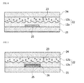
- FIGS. 1 to 3 are cross-sectional views showing an adhesive film according to one exemplary embodiment of the present invention.
- FIGS. 4 and 5 are cross-sectional views showing a product for encapsulating an OED according to one exemplary embodiment of the present invention.
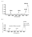
- FIG. 6 shows the Fourier transform infrared (FT-IR) analysis results of an adhesive film manufactured in Example 1.
- FIG. 7 shows the FT-IR analysis results of an adhesive film manufactured in Comparative Example 2.
- first, second, etc. may be used to describe various elements, these elements are not limited by these terms. These terms are only used to distinguish one element from another. For example, a first element could be termed a second element, and, similarly, a second element could be termed a first element, without departing from the scope of exemplary embodiments.
- the term "and/or" includes any and all combinations of one or more of the associated listed items.
- An adhesive film according to one exemplary embodiment of the present invention serves to encapsulate an organic electronic device (OED), and includes an adhesive layer having a multilayer structure.
- OED organic electronic device
- the adhesive film includes a curable hot-melt adhesive layer including a curable resin and a moisture absorbent
- the curable hot-melt adhesive layer includes a first region coming in contact with the OED upon encapsulation of the OED and a second region not coming in contact with the OED
- the moisture absorbent is present at contents of 0 to 20% and 80 to 100% in the first and second regions, respectively, based on the total weight of the moisture absorbent in the adhesive layer.
- organic electronic device refers to a product or device having a structure including an organic layer which generates an alternating current with electric charges through the combination of holes and electrons between a pair of facing electrodes
- OED organic electronic device
- examples of the OED may include a photovoltaic device, a rectifier, a transmitter and an organic light emitting diode (OLED), but the present invention is not limited thereto.
- the OED may be an OLED.
- hot-melt adhesive refers to a kind of an adhesive that may maintain a solid or semi-solid phase at room temperature, attach a plate without bubbles due to flowability exerted when heat is applied, and strongly fix a subject using an adhesive when a curing reaction is completed.
- the adhesive film according to the present invention may have a viscosity at room temperature of 10 6 dyne/cm 2 or more, and preferably 10 7 dyne/cm 2 or more.
- room temperature refers to a temperature at which an adhesive film is not heated or cooled, for example, a temperature of approximately 15 °C to 35 °C, more particularly approximately 20 °C to 25 °C, and further particularly approximately 25 °C.
- the viscosity may be measured using an advanced rheometric expansion system (ARES).
- ARES advanced rheometric expansion system
- problems such as contraction and volatile gas generation which may be caused by curing of a resin may be remarkably reduced to prevent the physical or chemical damage to an organic electronic device.
- an upper limit of the viscosity is not particularly limited.
- the viscosity may be controlled to a range of approximately 10 9 dyne/cm 2 or less in consideration of the processability.
- the adhesive film for encapsulating an OED has a multilayer structure, which includes a curable hot-melt adhesive layer including a curable resin and moisture absorbent, and the curable hot-melt adhesive layer includes a first region coming in contact with the OED upon encapsulation of the OED, and a second region not coming in contact with the OED.
- the moisture absorbent may be present at contents of 0 to 20% and 80 to 100% in the first and second regions, respectively, based on the total weight of the moisture absorbent in the curable hot-melt adhesive layer. When the content of the moisture absorbent in the first region closer to the OED exceeds 20%, the volume expansion caused by reaction of the moisture absorbent with moisture may not be controlled using only a curing resin, which leads to increased cracks in a film of the OED.
- the physical and chemical damage to the OED due to the presence of the moisture absorbent in the adhesive film used as an encapsulation material may be prevented by controlling the content of the moisture absorbent in the adhesive layer having such a multilayer structure and the first and second regions.
- Any method of forming an adhesive layer having a multilayer structure known in the art may be used without limitation as the method of dividing the adhesive layer into first and second regions so that the first and second regions can have a multilayer structure.
- the first and second regions of the adhesive layer may have the same or different kinds and contents of the other components, for example, a curable resin, a moisture absorbent, other additives, or a filler. Unless defined otherwise herein, the following description is related to both the first and second regions of the adhesive layer.
- the curable resin in a cured state may have a water vapor transmission rate (WVTR) of 50 g/m 2 ⁇ day or less, preferably 30 g/m 2 ⁇ day or less, more preferably 20 g/m 2 ⁇ day or less, and most preferably 15 g/m 2 ⁇ day or less.
- WVTR water vapor transmission rate
- the term "cured state of a curable resin” refers to a state in which a curable resin may be cured or crosslinked alone or by reaction with another component such as a curing agent so that the curable resin can maintain constant contents of a moisture absorbent and a filler and serve as a structural adhesive when the curable resin is used as an encapsulation material.
- the WVTR refers to a WVTR of a cured product which is measured at 38 °C and 100% relative humidity (R.H.) in a transverse direction when the cured product is formed by curing a curable resin and then processed into a film having a thickness of 80 ⁇ m. Also, the WVTR is measured according to the ASTM F1249 standard.
- the WVTR may be controlled to effectively prevent penetration of moisture, humidity or oxygen into a product for encapsulating an OED (hereinafter referred to as an "OED-encapsulating product") and effectively introduce a moisture-reactive absorbent into the OED-encapsulating product.
- OED-encapsulating product a product for encapsulating an OED
- a lower limit of the WVTR is not particularly limited.
- thermosetting resin refers to a resin that may be cured by proper application of heat or through an aging process
- photocurable resin refers to a resin that may be cured by irradiation with electromagnetic waves.
- a category of the electromagnetic waves described above may include a particle beam such as an ⁇ -particle beam, a proton beam, a neutron beam and an electron beam as well as microwaves, infrared rays (IR), ultraviolet rays (UV), X-rays and ⁇ -rays.
- the photocurable resin may be a cation-photocurable resin.
- the cation-photocurable resin refers to a resin that may be cured by a cation polymerization or cation curing reaction induced by irradiation with electromagnetic waves.
- the curable resin may be a dual curable resin showing both of the thermosetting and photocurable characteristics.
- the curable resin that may be cured to give an adhesive property may include resins that contain at least one functional group which can be cured by heat, such as a glycidyl group, an isocyanate group, a hydroxyl group, a carboxyl group or an amide group, or contain at least one functional group which can be cured by irradiation with electromagnetic waves, such as an epoxide group, a cyclic ether group, a sulfide group, an acetal group or a lactone group.
- specific kinds of such a resin may include an acryl resin, a polyester resin, an isocyanate resin or an epoxy resin, but the present invention is not limited thereto.
- an aromatic or aliphatic epoxy resin or a linear or branched epoxy resin may be used as the curable resin.
- an epoxy resin having an epoxy equivalent weight of 180 g/eq to 1,000 g/eq may be used as the epoxy resin containing at least two functional groups.
- the epoxy resin having the above-described epoxy equivalent weight range may be used to effectively maintain the characteristics such as adhesion and glass transition temperature of a cured product.
- Examples of such an epoxy resin may include a cresol novolac epoxy resin, a bisphenol A-type epoxy resin, a bisphenol A-type novolac epoxy resin, a phenol novolac epoxy resin, a tetrafunctional epoxy resin, a biphenyl-type epoxy resin, a triphenolmethane-type epoxy resin, an alkyl-modified triphenolmethane epoxy resin, a naphthalene-type epoxy resin, a dicyclopentadiene-type epoxy resin or a dicyclopentadiene-modified phenol-type epoxy resin, which may be used alone or in combination.
- an epoxy resin having a ring structure in the molecular structure may be preferably used, and an epoxy resin containing an aromatic group (for example, a phenyl group) may be more preferably used herein.
- an epoxy resin containing an aromatic group for example, a phenyl group
- a cured product of the epoxy resin has excellent thermal and chemical stabilities and also shows low moisture absorption, which leads to improved reliability of an encapsulation structure of the OED.
- aromatic group-containing epoxy resin may include, but are not limited to, a biphenyl-type epoxy resin, a dicyclopentadiene-type epoxy resin, a naphthalene-type epoxy resin, a dicyclopentadiene-modified phenol-type epoxy resin, a cresol-based epoxy resin, a bisphenol-based epoxy resin, a xyloxy-based epoxy resin, a multifunctional epoxy resin, a phenol novolac epoxy resin, a triphenolmethane-type epoxy resin and an alkyl-modified triphenolmethane epoxy resin, which may be used alone or in combination.
- a silane-modified epoxy resin having a silane-modified epoxy resin, preferably an aromatic group may be more preferably used as the epoxy resin.
- the epoxy resin is structurally modified with silane so that it can have a silane group, it is possible to maximize an adhesive property to materials for a glass substrate or inorganic substrate of the OED and also improve properties such as a moisture barrier property, durability and reliability.
- Specific kinds of such an epoxy resin that may be used herein are not particularly limited, and the epoxy resin may be, for example, easily purchased from a manufacturer such as Kukdo Chemical Co., Ltd.
- the curable hot-melt adhesive layer according to the present invention includes a moisture absorbent in addition to the curable resin.
- moisture absorbent refers to a general component that can absorb or remove moisture or humidity, which is flowing in from the outside, by physical or chemical reaction. That is, the moisture absorbent means a moisture-reactive absorbent or physical absorbent, and a mixture thereof may also be used herein.
- the moisture-reactive absorbent serves to absorb moisture or humidity by chemical reaction with humidity, moisture or oxygen introduced into an adhesive layer.
- the physical absorbent may suppress moisture or humidity from penetrating into an encapsulation structure by increasing a travel path of the moisture or humidity and maximize a barrier property to moisture and humidity by interaction with a matrix structure of the curable resin and a moisture-reactive absorbent.
- the moisture absorbent may include a small amount of the moisture-reactive absorbent in the first region of the adhesive layer of the adhesive film.
- the moisture absorbent may include a metal powder, a metal oxide (e.g., alumina), a metal salt, phosphorus pentoxide (P 2 O 5 ), or a mixture thereof, and the physical absorbent may include silica, zeolite, titania, zirconia or montmorillonite.
- a metal powder e.g., alumina
- a metal salt e.g., phosphorus pentoxide (P 2 O 5 )
- P 2 O 5 phosphorus pentoxide
- the physical absorbent may include silica, zeolite, titania, zirconia or montmorillonite.
- the metal oxide described above may include lithium oxide (Li 2 O), sodium oxide (Na 2 O), barium oxide (BaO), calcium oxide (CaO) or magnesium oxide (MgO), and examples of the metal salt may include, but are not limited to, a sulfate such as lithium sulfate (Li 2 SO 4 ), sodium sulfate (Na 2 SO 4 ), calcium sulfate (CaSO 4 ), magnesium sulfate (MgSO 4 ), cobalt sulfate (CoSO 4 ), gallium sulfate (Ga 2 (SO 4 ) 3 ), titanium sulfate (Ti(SO 4 ) 2 ) or nickel sulfate (NiSO 4 ); a metal halide such as calcium chloride (CaCl 2 ), magnesium chloride (MgCl 2 ), strontium chloride (SrCl 2 ), yttrium chloride (YCl 3 ), copper chloride (CuCl
- the moisture absorbent such as a metal oxide may be properly processed and blended with a composition.
- the adhesive layer may be a thin film having a thickness of 30 ⁇ m or less according to the kind of the OED to which an adhesive film is applied.
- a process of grinding a moisture absorbent is required.
- the grinding of the moisture absorbent may be performed using a process such as 3-roll milling, bead milling or ball milling.
- the adhesive film of the present invention is used in top emission-type OEDs, the permeability of the adhesive layer itself is very important, and thus the moisture absorbent should be decreased in size. Thus, the grinding process may be required in such applications.
- the second region of the curable hot-melt adhesive layer according to the present invention may include the moisture absorbent at a content of 1 part by weight to 100 parts by weight, preferably 5 parts by weight to 50 parts by weight, based on 100 parts by weight of the curable resin.
- a cured product may show an excellent barrier property to moisture and humidity.
- a cured product may show an excellent barrier property to moisture when forming an encapsulation structure of a thin film.
- the unit "parts by weight” refers to a weight ratio of each component.
- the first region of the curable hot-melt adhesive layer according to the present invention may also include the moisture absorbent at a content of 0 parts by weight to 20 parts by weight, based on 100 parts by weight of the curable resin.
- the content of the moisture absorbent is 0 parts by weight, the moisture absorbent is not present in the first region of the curable hot-melt adhesive layer, but is present only in the second region.
- the content of the moisture absorbent is controlled to 20 parts by weight or less, it is possible to maximize a barrier property to moisture and also minimize physical and chemical damage to the OED caused by the presence of the moisture absorbent.
- the curable hot-melt adhesive layers of the first and second regions according to the present invention may include a filler, preferably an inorganic filler.
- the filler may suppress moisture or humidity from penetrating into an encapsulation structure by increasing a travel path of the moisture or humidity, and maximize a barrier property to moisture and humidity by interaction with a matrix structure of the curable resin and a moisture-reactive absorbent.
- Specific kinds of the filler that may be used herein are not particularly limited. For example, clay, talc, acicular silica, or a mixture of at least one thereof may be used alone or in combination.
- a product surface-treated with an organic material may be used as the filler, or may also be used together with a coupling agent.
- the curable hot-melt adhesive layer according to the present invention may include the filler at a content of 1 part by weight to 50 parts by weight, preferably 1 part by weight to 20 parts by weight, based on 100 parts by weight of the curable resin.
- a cured product having an excellent barrier property to moisture or humidity and excellent mechanical properties may be provided.
- the curable resin may be prepared in the form of a film, and a cured product showing an excellent barrier property to moisture or humidity even when the curable resin is formed into a thin film may also be provided.
- the curable hot-melt adhesive layers of the first and second regions according to the present invention may further include a curing agent which can react with a curable resin to form a matrix such as a cross-linking structure.
- the curing agent may include, but is not limited to, various compounds such as an amine-based compound, an imidazole-based compound, a phenol-based compound, a phosphorus-based compound or an acid anhydride-based compound, which may be used alone or in combination.
- the curable hot-melt adhesive layers of the first and second regions according to the present invention may, for example, include the curing agent at a content of 1 part by weight to 20 parts by weight, preferably 1 part by weight to 10 parts by weight, based on 100 parts by weight of the thermosetting resin.
- the content of the thermosetting resin is merely one exemplary embodiment of the present invention. That is, the content of the curing agent may be varied in the present invention according to the kind and content of the curable resins or their functional groups, the matrix structure to be realized, or the cross-linking density.
- the curable hot-melt adhesive layer according to the present invention may further include a high molecular weight resin.
- the high molecular weight resin may serve to improve formability when a composition according to the present invention is shaped in the form of a film or sheet. Also, the high molecular weight resin may serve as a high-temperature viscosity controlling agent for controlling the flowability during a hot-melting process.
- kinds of the high molecular weight resin that may be used herein are not particularly limited as long as they have compatibility with other components such as a curable resin.
- Specific examples of the high molecular weight resin that may be used herein may include, but are not limited to, resins having a weight average molecular weight of 20,000 or more, for example, a phenoxy resin, an acrylate resin, a high molecular weight epoxy resin, a super-high molecular weight epoxy resin, a high-polarity functional group-containing rubber and a high-polarity functional group-containing reactive rubber, which may be used alone or in combination.
- the content of the high molecular weight resin is controlled according to the desired physical properties, but the present invention is not particularly limited thereto.
- the high molecular weight resin may be included at a content of approximately 200 parts by weight or less, preferably 150 parts by weight or less, and more preferably approximately 100 parts by weight or less, based on 100 parts by weight of the curable resin.
- the high molecular weight when the content of the high molecular weight resin is controlled to 200 parts by weight or less, the high molecular weight may effectively maintain the compatibility with each component of a resin composition, and also function as an adhesive.
- the adhesive film according to the present invention may further include an additional additive such as a filler for improving the durability of a cured product, a coupling agent for improving the mechanical and adhesive strengths, a UV stabilizer and an antioxidant, without departing from the scope of the present invention.
- an additional additive such as a filler for improving the durability of a cured product, a coupling agent for improving the mechanical and adhesive strengths, a UV stabilizer and an antioxidant, without departing from the scope of the present invention.
- a structure of the adhesive film according to the present invention is not particularly limited as long as the structure of the adhesive film includes the adhesive layer.
- the adhesive film according to the present invention may have a structure including a base film or release film (hereinafter referred to as a "first film"); and an adhesive layer formed on the base film or release film.
- the adhesive film according to the present invention may further include a base film or release film (hereinafter referred to as a "second film") formed on the adhesive layer.
- a base film or release film hereinafter referred to as a "second film”
- FIGS. 1 to 3 are cross-sectional views showing an adhesive film according to one exemplary embodiment of the present invention.
- the adhesive film according to the present invention may include an adhesive layer 12 formed on a base film or release film 11.
- FIG. 1 shows that a moisture absorbent is present only in a second region of an adhesive layer included in the adhesive film according to the present invention
- FIG. 2 shows that a small amount of a moisture absorbent is also present in a first region.
- the adhesive film according to the present invention may further include a base film or release film 14 formed on the adhesive layer 12, as shown in FIG. 3 .
- the adhesive film as shown in FIG. 3 is merely one exemplary embodiment of the present invention, and a stacking sequence of the first and second regions of the adhesive layer may be reversed, when necessary.
- the first film that may be used herein are not particularly limited.
- a typical polymer film known in the art may, for example, be used as the first film.
- the base film or release film that may be used herein may, for example, include a polyethylene terephthalate film, a polytetrafluoroethylene film, a polyethylene film, a polypropylene film, a polybutene film, a polybutadiene film, a vinyl chloride copolymer film, a polyurethane film, an ethylene-vinyl acetate film, an ethylene-propylene copolymer film, an ethylene-acrylic acid ethyl copolymer film, an ethylene-acrylic acid methyl copolymer film or a polyimide film.
- a release agent used to release a base film may include an alkyd-based release agent, a silicone-based release agent, a fluorine-based release agent, an unsaturated ester-based release agent, a polyolefin-based release agent or a wax-based release agent.
- an alkyd-based, silicone-based or fluorine-based release agent may be preferably used in an aspect of heat resistance, but the present invention is not limited thereto.
- kinds of a second film that may be used herein are not particularly limited.
- the same or different kind of the first film may be used as the second film when a range of the second film falls within the above-described range of the first film.
- the second film may also be subjected to release treatment, and used.
- the thickness of such a base film or release film is not particularly limited, and may be properly selected according to applications.
- the thickness of the first film may be, for example, in a range of 10 ⁇ m to 500 ⁇ m, preferably 20 ⁇ m to 200 ⁇ m.
- the thickness of the first film is less than 10 ⁇ m, a base film may be easily deformed during a manufacturing process, whereas an economical efficiency may be degraded when the thickness of the first film exceeds 500 ⁇ m.
- the thickness of the second film is not particularly limited. According to the present invention, the thickness of the second film may be, for example, set to the same thickness as the first film. According to the present invention, the thickness of the second film may also be set to a relatively smaller thickness than the first film in consideration of the processability.
- the thickness of the adhesive layer included in the adhesive film according to the present invention is not particularly limited, but may be properly selected according to the following conditions in consideration of applications of the adhesive film.
- the first region of the adhesive layer preferably has a smaller thickness than the second region.
- the first region of the adhesive layer may have a thickness of 1 ⁇ m to 20 ⁇ m, preferably 2 ⁇ m to 15 ⁇ m
- the thickness of the first region is less than 1 ⁇ m, the ability of the second region of the adhesive layer to protect the OED from damage factors may be degraded, for example, even when the adhesive film is used as an encapsulation material for OEDs.
- the second region of the adhesive layer may have a thickness of 5 ⁇ m to 200 ⁇ m, preferably 5 ⁇ m to 100 ⁇ m.
- the thickness of the second region is less than 5 ⁇ m, the ability to prevent penetration of moisture may be insufficient.
- the thickness of the second region exceeds 200 ⁇ m, it is difficult to secure the processability, damage may be caused to a deposited film of an organic EL element as the expansion in thickness is increased due to the reactivity with moisture, and the economical efficiency may be degraded.
- each of the first and second regions of the adhesive film may be prepared using a method including a first operation of coating a base film or release film with a coating solution including a composition of the above-described adhesive layer; and a second operation of drying the coating solution coated in the first operation.
- a method of stacking each of the first and second regions is not particularly limited.
- an adhesive film having a multilayer structure may be formed by joining first and second regions formed respectively on separate release films to each other, and a second region may be directly formed on a first region, or vice versa.
- the method of manufacturing an adhesive film according to the present invention may further include a third operation of further compressing the base film or release film onto the coating solution dried in the second operation.
- the first operation according to the present invention is to prepare a coating solution by dissolving or dispersing the above-described composition of the adhesive layer in a proper solvent.
- the content of the epoxy resin included in the coating solution may be properly controlled according to the desired properties such as a barrier property to moisture and film formability.
- kinds of the solvent used in preparation of the coating solution are not particularly limited.
- a drying time of the solvent is too long, or the solvent is dried at a high temperature, the workability or the durability of the adhesive film may be deteriorated. Therefore, the use of a solvent having an evaporation temperature of 100 °C or lower is preferred.
- a small amount of the solvent having an evaporation temperature greater than this temperature range may be used in consideration of the film formability.
- solvent examples include, but are not limited to, methylethylketone (MEK), acetone, toluene, dimethylformamide (DMF), methylcellosolve (MCS), tetrahydrofuran (THF) or N-methylpyrrolidone (NMP), which may be used alone or in combination.
- MEK methylethylketone
- DMF dimethylformamide
- MCS methylcellosolve
- THF tetrahydrofuran
- NMP N-methylpyrrolidone
- a method of coating a base film or release film with such a coating solution is not particularly limited.
- a known method such as knife coating, roll coating, spray coating, gravure coating, curtain coating, comma coating or lip coating may be used without limitation.
- the second operation of the present invention is to form an adhesive layer by drying the coating solution coated in the first operation. That is, in the second operation of the present invention, an adhesive layer may be formed by heating the coating solution coated on the film to dry the film and remove the solvent.
- the drying conditions are not particularly limited. For example, the drying process may be performed at a temperature of 70 °C to 200 °C for 1 to 10 minutes.
- a third operation of compressing an additional base film or release film onto the adhesive layer formed on the film may be further performed after the second operation.
- Such a third operation of the present invention may be performed by compressing an additional release film or base film (a cover film or second film) onto the dried adhesive layer after coating the film using a hot-roll lamination or press process.
- the third operation may be performed using a hot-roll lamination process in aspects of the probability and efficiency of a continuous process.
- the process may be performed at a temperature of approximately 10 °C to 100 °C and a pressure of approximately 0.1 kgf/cm 2 to 10 kgf/cm 2 .
- Another exemplary embodiment of the present invention is directed to providing an OED-encapsulating product including a substrate, an OED formed on the substrate, and an adhesive film described above for encapsulating the OED.
- a first region of the adhesive layer of the adhesive film covers the OED.
- the OED may be an organic light emitting diode (OLED).
- the OED-encapsulating product may further include a passivation film formed between the adhesive film and the OED for protecting the OED.
- Still another exemplary embodiment of the present invention is directed to providing a method of encapsulating an OED including applying an adhesive film to a substrate having the OED formed therein so that a first region of an adhesive layer of the adhesive film can cover the OED; and curing the adhesive layer.
- An operation of applying the OED to the adhesive film may be performed by subjecting the adhesive film to a hot-roll lamination, hot press or vacuum press method, but the present invention is not particularly limited thereto.
- the operation of applying the OED to the adhesive film may be performed at a temperature of 50 °C to 90 °C, and the curing may be performed by heating the adhesive layer at a temperature of 70 °C to 110°C or irradiating the adhesive layer with UV rays.
- the method of encapsulating an OED may further include attaching a second region of the adhesive film to an additional encapsulation material such as a glass or a metal so that the second region and the encapsulation material can come in contact with each other.
- an additional encapsulation material such as a glass or a metal
- FIG. 4 is a cross-sectional view of an OED-encapsulating product according to one exemplary embodiment of the present invention.
- a transparent electrode is formed on a substrate 21 such as a glass or polymer film using a method such as vacuum deposition or sputtering, and an organic layer is formed on the transparent electrode.
- the organic layer may include a hole injection layer, a hole transfer layer, a light emitting layer, an electron injection layer and/or an electron transfer layer.
- a second electrode is further formed on the organic layer.
- the above-described adhesive film 22 is applied onto the OED 25 formed on the substrate 21 so that the adhesive film 22 can cover the entire organic electronic device 25.
- a method of applying the adhesive film 22 is not particularly limited.
- a cover substrate (e.g., a glass or polymer film) 24 to which the adhesive layer of the adhesive film according to the present invention has been previously transferred may be applied onto the OED 25 formed on the substrate 21 using a method such as heating or compression.
- a method such as heating or compression.
- the adhesive film 22 when the adhesive film 22 is transferred onto the cover substrate 24, the above-described adhesive film according to the present invention may be transferred onto the cover substrate 24 using a vacuum press or vacuum laminator while the base film or release film formed on the adhesive film is peeled off and heated.
- the close adhesion and adhesive strength of the adhesive film 22 may be degraded.
- a process temperature and a processing time it is desirable to control a process temperature and a processing time to approximately 100 °C or lower and 5 minutes, respectively.
- a vacuum press or vacuum laminator may be used.
- the temperature condition may be set as described above, and the processing time may be set to less than 10 minutes.
- the adhesive film is applied to the OED so that the adhesive layer of the first region rather than the second region of the adhesive film can come in contact with the OED (in contact with a passivation film when the OED includes the passivation film).
- the adhesive film to which the OED is compressed may also be further subjected to a curing process.
- the curing process (the inventive curing) may be, for example, performed in a heating chamber or a UV chamber.
- the conditions in the inventive curing may be properly selected in consideration of the stability of the OED.
- the above-described manufacturing process is merely one exemplary embodiment for encapsulating the OED according to the present invention.
- the process sequence and process conditions may be easily changed.
- the sequence of the transfer and compressing process may be changed in the present invention in such a manner that the adhesive film 22 according to the present invention is first transferred onto the OED 25 formed on the substrate 21 and the cover substrate 24 is compressed.
- the adhesive film 22 may be applied to the passivation layer, and cured without forming the cover substrate 24.
- the moisture absorbent solution as previously prepared above was added to the homogenized solution, and 4 g of a curing agent, imidazole (Shikoku Chemicals Corporation), was added, and stirred at a high speed for 1 hour to prepare a solution for a second region.
- a curing agent imidazole (Shikoku Chemicals Corporation)
- the solution for a first region as previously prepared above was applied to a released surface of a release PET film using a comma coater, and dried at 130 °C for 3 minutes in an oven to form an adhesive layer having a thickness of 15 ⁇ m
- the solution for a second region as previously prepared above was applied to a released surface of a release PET film using a comma coater, and dried at 130 °C for 3 minutes in an oven to form an adhesive layer having a thickness of 15 ⁇ m.
- the adhesive layers of the first and second regions were joined together to manufacture a multilayer adhesive film.
- An adhesive film having a multilayer structure was manufactured in the same manner as in Example 1, except that 7 g of CaO was added to the first region solution and 62 g of CaO was added to the second region solution in the manufacture of the adhesive film of Example 1.
- An adhesive film having a multilayer structure was manufactured in the same manner as in Example 1, except that 14 g of CaO was added to the first region solution and 56 g of CaO was added to the second region solution in the manufacture of the adhesive film of Example 1.
- An adhesive film having a thickness of 45 ⁇ m was manufactured in the same manner as in the manufacture of the adhesive film of Example 1, except that only compositions of the first region solution prepared in Example 1 were used.
- An adhesive film having a thickness of 45 ⁇ m was manufactured in the same manner as in the manufacture of the adhesive film of Example 1, except that only compositions of the second region solution prepared in Example 1 were used.
- An adhesive film having a multilayer structure was manufactured in the same manner as in Example 1, except that 28 g of CaO was added to the first region solution and 42 g of CaO was added to the second region solution in the manufacture of the adhesive film of Example 1.
- An adhesive film having a multilayer structure was manufactured in the same manner as in Example 1, except that the silane-modified epoxy resin was exchanged with an acryl pressure-sensitive adhesive resin in the manufacture of the adhesive film of Example 1.
- An adhesive film having a multilayer structure was manufactured in the same manner as in Example 1, except that the silane-modified epoxy resin was exchanged with a butadiene-modified epoxy resin in the manufacture of the adhesive film of Example 1.
- a calcium test was carried out. More particularly, calcium (Ca) was deposited on a glass substrate having a size of 100 mm ⁇ 100 mm to form 9 spots with a size of 5 mm ⁇ 5 mm and a thickness of 100 nm, and a cover glass to which each of the adhesive films of Examples 1 to 3 and Comparative Examples 1 to 3 was transferred was heated at each calcium-deposited spot at 80 °C for 1 minute using a vacuum press method.
- each of the adhesive films was cured at 100 °C for 3 hours in a high-temperature oven, and the encapsulated Ca test sample was then cut into pieces with a size of 11 mm ⁇ 11 mm.
- the obtained test samples were kept under conditions of a temperature of 85 °C and 85% R.H. in a constant temperature and humidity chamber, and a time point where a Ca-containing coating solution started to show transparency due to an oxidation reaction with penetrating moisture was determined. The results are listed in the following Table 1.
- the curable resins in the adhesive films manufactured in Example 1 and Comparative Examples 4 to 5 were measured for WVTR.
- the WVTR measurement was performed by curing a silane-modified epoxy resin, an acryl pressure-sensitive adhesive resin and a butadiene-modified epoxy resin to form films having a thickness of 80 ⁇ m and measuring WVTRs of the films in a transverse direction at 38 °C and 100% R.H. using equipment commercially available from MOCON.
- the results are listed in the following Table 2.
- SiNx Silicon nitride used for a passivation film in the OED was deposited on a glass to a thickness of 1 ⁇ m.
- the adhesive films of Examples 1 to 3 according to the exemplary embodiments of the present invention may serve to effectively encapsulate the OED from moisture, but effective encapsulation of the OED is not attained when the first and second regions are not demarcated in the adhesive film or at least a certain content of the moisture absorbent is included in the first region.
- the adhesive film according to the present invention may be useful in effectively preventing moisture or oxygen flowing in the OED from penetrating from the outside and also improving the lifespan and durability of the OED.
Landscapes
- Chemical & Material Sciences (AREA)
- Organic Chemistry (AREA)
- Physics & Mathematics (AREA)
- Optics & Photonics (AREA)
- Engineering & Computer Science (AREA)
- Inorganic Chemistry (AREA)
- Condensed Matter Physics & Semiconductors (AREA)
- General Physics & Mathematics (AREA)
- Computer Hardware Design (AREA)
- Microelectronics & Electronic Packaging (AREA)
- Power Engineering (AREA)
- Polymers & Plastics (AREA)
- Medicinal Chemistry (AREA)
- Chemical Kinetics & Catalysis (AREA)
- Health & Medical Sciences (AREA)
- Manufacturing & Machinery (AREA)
- Materials Engineering (AREA)
- Dispersion Chemistry (AREA)
- Electroluminescent Light Sources (AREA)
- Adhesives Or Adhesive Processes (AREA)
- Adhesive Tapes (AREA)
- Manufacture Of Macromolecular Shaped Articles (AREA)
- Compositions Of Macromolecular Compounds (AREA)
- Structures Or Materials For Encapsulating Or Coating Semiconductor Devices Or Solid State Devices (AREA)
Applications Claiming Priority (4)
| Application Number | Priority Date | Filing Date | Title |
|---|---|---|---|
| KR20100108113 | 2010-11-02 | ||
| KR20110004054 | 2011-01-14 | ||
| PCT/KR2011/008280 WO2012060621A2 (ko) | 2010-11-02 | 2011-11-02 | 접착 필름 및 이를 이용한 유기전자장치의 봉지 방법 |
| KR1020110113121A KR101293803B1 (ko) | 2010-11-02 | 2011-11-02 | 접착 필름 및 이를 이용한 유기전자장치의 봉지 방법 |
Publications (3)
| Publication Number | Publication Date |
|---|---|
| EP2637229A2 true EP2637229A2 (de) | 2013-09-11 |
| EP2637229A4 EP2637229A4 (de) | 2014-06-18 |
| EP2637229B1 EP2637229B1 (de) | 2018-01-03 |
Family
ID=46265725
Family Applications (1)
| Application Number | Title | Priority Date | Filing Date |
|---|---|---|---|
| EP11838226.6A Active EP2637229B1 (de) | 2010-11-02 | 2011-11-02 | Klebefilm und verfahren zum einkapseln einer organischen elektronischen vorrichtung damit |
Country Status (7)
| Country | Link |
|---|---|
| US (5) | US8742411B2 (de) |
| EP (1) | EP2637229B1 (de) |
| JP (2) | JP5885356B2 (de) |
| KR (9) | KR101293803B1 (de) |
| CN (5) | CN107722894A (de) |
| TW (2) | TWI444449B (de) |
| WO (1) | WO2012060621A2 (de) |
Cited By (10)
| Publication number | Priority date | Publication date | Assignee | Title |
|---|---|---|---|---|
| EP2781568A1 (de) * | 2011-11-14 | 2014-09-24 | LG Chem, Ltd. | Haftfilm und verfahren zum einkapseln einer organischen elektronischen vorrichtung damit |
| CN105073884A (zh) * | 2013-09-24 | 2015-11-18 | Lg化学株式会社 | 可固化组合物 |
| EP2835841A4 (de) * | 2012-08-03 | 2015-11-25 | Lg Chemical Ltd | Klebefilm und abdichtungsverfahren für organische elektronische vorrichtung damit |
| CN105219285A (zh) * | 2014-07-01 | 2016-01-06 | 利诺士有限公司 | 有机电子装置用粘合膜及包含该粘合膜的有机电子装置用封装材料 |
| WO2016096937A1 (en) * | 2014-12-18 | 2016-06-23 | Rolic Ag | Radiation curable composition comprising hydrophilic nanoparticles |
| EP3001478A4 (de) * | 2013-05-21 | 2017-01-25 | LG Chem, Ltd. | Einkapselungsfilm und verfahren zum einkapseln einer organischen elektronischen vorrichtung damit |
| EP3001476A4 (de) * | 2013-05-21 | 2017-01-25 | LG Chem, Ltd. | Einkapselungsfilm und verfahren zum einkapseln einer organischen elektronischen vorrichtung damit |
| EP3012285A4 (de) * | 2013-06-19 | 2017-03-01 | LG Chem, Ltd. | Beutelmaterialfolie |
| EP2644677A4 (de) * | 2010-11-23 | 2017-03-15 | LG Chem, Ltd. | Haftzusammensetzung |
| US9698378B2 (en) | 2012-01-06 | 2017-07-04 | Lg Chem, Ltd. | Encapsulation film |
Families Citing this family (68)
| Publication number | Priority date | Publication date | Assignee | Title |
|---|---|---|---|---|
| US9935289B2 (en) | 2010-09-10 | 2018-04-03 | Industrial Technology Research Institute Institute | Environmental sensitive element package and encapsulation method thereof |
| EP2445028A1 (de) * | 2010-10-25 | 2012-04-25 | Nederlandse Organisatie voor toegepast -natuurwetenschappelijk onderzoek TNO | Optoelektrische Vorrichtung und Verfahren zur Herstellung einer optoelektrischen Vorrichtung |
| JP5885356B2 (ja) * | 2010-11-02 | 2016-03-15 | エルジー・ケム・リミテッド | 接着フィルム及びこれを利用した有機電子装置の封止方法 |
| DE102011084276B4 (de) | 2011-10-11 | 2019-10-10 | Osram Oled Gmbh | Verkapselung für ein organisches elektronisches bauelement, ein organisches elektronisches bauelement mit der verkapselung und ein verfahren zur herstellung eines organischen elektronischen bauelements mit der verkapselung |
| KR101424395B1 (ko) * | 2012-05-31 | 2014-07-28 | 주식회사 엘지화학 | 유기전자장치의 제조방법 |
| WO2014021687A1 (ko) * | 2012-08-02 | 2014-02-06 | 주식회사 엘지화학 | 접착 필름 및 이를 이용한 유기전자장치의 봉지 방법 |
| CN104685018B (zh) * | 2012-08-02 | 2017-02-22 | Lg化学株式会社 | 粘合膜和使用该粘合膜封装有机电子器件的方法 |
| TWI558787B (zh) | 2012-08-03 | 2016-11-21 | Lg化學股份有限公司 | 黏合膜及使用彼之有機電子裝置的包封產品 |
| WO2014021696A1 (ko) * | 2012-08-03 | 2014-02-06 | 주식회사 엘지화학 | 접착 필름 및 이를 이용한 유기전자장치의 봉지 제품 |
| WO2014021697A1 (ko) * | 2012-08-03 | 2014-02-06 | 주식회사 엘지화학 | 접착 필름 및 이를 이용한 유기전자장치의 봉지 제품 |
| KR101518125B1 (ko) * | 2012-08-03 | 2015-05-07 | 주식회사 엘지화학 | 접착 필름 및 이를 이용한 유기전자장치의 봉지 제품 |
| KR20140031003A (ko) | 2012-09-04 | 2014-03-12 | 삼성디스플레이 주식회사 | 유기 발광 표시 장치 및 그 제조 방법 |
| TWI500198B (zh) * | 2012-09-19 | 2015-09-11 | Innocom Tech Shenzhen Co Ltd | 顯示面板 |
| WO2014109330A1 (ja) * | 2013-01-10 | 2014-07-17 | 宇部マテリアルズ株式会社 | 水分吸着剤及びその製造方法 |
| CN103199199B (zh) * | 2013-03-05 | 2016-06-01 | 京东方科技集团股份有限公司 | 一种oled器件封装薄膜、制备方法以及oled器件、封装方法 |
| KR102135453B1 (ko) * | 2013-05-24 | 2020-07-20 | 삼성디스플레이 주식회사 | 접착필름 및 이를 이용해 제조된 유기전계발광 표시장치 |
| EP3012284B1 (de) | 2013-06-19 | 2020-08-26 | LG Chem, Ltd. | Zusammensetzung für verkapselungsmaterialfolie, verkapselungsmaterialfolie und elektronische vorrichtung damit |
| KR102153394B1 (ko) | 2013-07-29 | 2020-09-08 | 엘지디스플레이 주식회사 | 유기발광 표시장치 |
| KR20150016878A (ko) | 2013-08-05 | 2015-02-13 | 주식회사 엘지화학 | 점착제 조성물, 점착 필름 및 이를 이용한 유기전자장치의 봉지방법 |
| KR101726910B1 (ko) * | 2013-11-07 | 2017-04-13 | 제일모직주식회사 | 유기발광소자 충진용 접착시트 및 이의 제조방법 |
| KR102058550B1 (ko) * | 2013-12-27 | 2019-12-24 | 엘지디스플레이 주식회사 | 유기발광소자표시장치 제조방법 |
| KR20150097359A (ko) * | 2014-02-18 | 2015-08-26 | 주식회사 엘지화학 | 봉지 필름 및 이를 포함하는 유기전자장치 |
| WO2015136581A1 (ja) * | 2014-03-12 | 2015-09-17 | パナソニック株式会社 | 有機el装置 |
| WO2015141512A1 (ja) * | 2014-03-19 | 2015-09-24 | リンテック株式会社 | 電子素子封止用積層シートおよび電子デバイスの製造方法 |
| EP3125328B1 (de) * | 2014-03-27 | 2022-12-14 | LG Chem, Ltd. | Versiegelungsfilm und organische elektronische vorrichtung damit |
| KR102203908B1 (ko) * | 2014-06-17 | 2021-01-14 | 엘지디스플레이 주식회사 | 접착 필름, 이를 이용한 유기 발광 표시 장치 및 유기 발광 표시 장치 제조 방법 |
| KR102245276B1 (ko) * | 2014-07-08 | 2021-04-26 | 엘지디스플레이 주식회사 | 유기 발광 표시 장치 봉지용 접착 수지 및 이를 이용한 유기 발광 표시 장치의 제조 방법 |
| KR101561103B1 (ko) * | 2014-12-17 | 2015-10-19 | 주식회사 이녹스 | 유기전자장치용 접착필름 및 이를 포함하는 유기전자장치용 봉지재 |
| EP3034548A1 (de) * | 2014-12-18 | 2016-06-22 | Nederlandse Organisatie voor toegepast- natuurwetenschappelijk onderzoek TNO | Sperrfolienlaminat enthaltend Submikrongetterpartikel und elektronische Vorrichtung mit solch einem Laminat |
| US9847509B2 (en) | 2015-01-22 | 2017-12-19 | Industrial Technology Research Institute | Package of flexible environmental sensitive electronic device and sealing member |
| KR102261689B1 (ko) * | 2015-03-24 | 2021-06-07 | 주식회사 엘지화학 | 접착제 조성물, 이를 포함하는 접착 필름, 이를 포함하는 유기전자장치 및 상기 유기전자장치의 제조 방법 |
| KR102351121B1 (ko) | 2015-04-24 | 2022-01-17 | 삼성디스플레이 주식회사 | 플렉서블 기판 및 그의 제조방법, 플렉서블 기판을 구비한 플렉서블 표시장치 |
| DE102015106982A1 (de) * | 2015-05-05 | 2016-11-10 | Lisa Dräxlmaier GmbH | Zeolithhaltige Heißschmelzklebe-, Heißschmelzdicht- und Heißklebebeschichtungsmassen |
| JP2017004747A (ja) * | 2015-06-10 | 2017-01-05 | 双葉電子工業株式会社 | 有機el表示装置 |
| JP6748878B2 (ja) * | 2015-09-01 | 2020-09-02 | パナソニックIpマネジメント株式会社 | 光導波路用組成物、光導波路用ドライフィルム、及び光導波路 |
| KR102416347B1 (ko) * | 2015-09-11 | 2022-07-01 | 엘지디스플레이 주식회사 | 유기발광 표시장치 |
| KR102404648B1 (ko) * | 2015-09-21 | 2022-05-31 | 엘지디스플레이 주식회사 | 표시장치 |
| KR102533756B1 (ko) * | 2015-09-22 | 2023-05-18 | 엘지디스플레이 주식회사 | 유기발광 표시장치 |
| KR101880209B1 (ko) * | 2015-09-25 | 2018-07-20 | 주식회사 엘지화학 | 지시 필름 |
| KR102411420B1 (ko) * | 2015-10-31 | 2022-06-20 | 엘지디스플레이 주식회사 | 유기 발광 표시 장치 및 그의 제조 방법 |
| KR102446199B1 (ko) * | 2015-11-19 | 2022-09-21 | 엘지디스플레이 주식회사 | 유기 발광 표시 장치 |
| KR20170079877A (ko) * | 2015-12-31 | 2017-07-10 | 주식회사 동진쎄미켐 | 접착필름의 봉지 기술을 이용한 유기전자소자 및 이의 제조 방법 |
| TWI641478B (zh) | 2016-03-11 | 2018-11-21 | Lg化學股份有限公司 | 包封膜 |
| US10593908B2 (en) * | 2016-04-12 | 2020-03-17 | Lg Chem, Ltd. | Encapsulation film |
| WO2017218500A1 (en) | 2016-06-16 | 2017-12-21 | 3M Innovative Properties Company | Nanoparticle filled barrier adhesive compositions |
| EP3472253A4 (de) | 2016-06-16 | 2019-12-25 | 3M Innovative Properties Company | Mit nanopartikeln gefüllte barrierehaftzusammensetzungen |
| KR20180013443A (ko) * | 2016-07-29 | 2018-02-07 | 가부시키가이샤 가네카 | 수분차단용 봉지 수지 조성물 |
| WO2018052006A1 (ja) * | 2016-09-16 | 2018-03-22 | 積水化学工業株式会社 | 有機エレクトロルミネッセンス表示素子用封止剤 |
| JP6719662B2 (ja) | 2016-09-30 | 2020-07-08 | エルジー・ケム・リミテッド | 接着剤組成物 |
| CN109148733B (zh) * | 2017-06-19 | 2020-09-22 | Tcl科技集团股份有限公司 | 一种基于金属粒子与吸附粒子交联的器件封装方法 |
| KR101862090B1 (ko) * | 2017-06-29 | 2018-06-29 | 신화인터텍 주식회사 | 접합 필름 및 이를 포함하는 유기전자장치 |
| CN109096932B (zh) * | 2017-06-29 | 2020-03-24 | 新和因特泰科株式会社 | 粘附膜以及包含上述粘附膜的有机电子装置 |
| KR101962193B1 (ko) * | 2017-08-22 | 2019-03-26 | (주)이녹스첨단소재 | 유기전자장치 봉지재용 접착필름 및 이를 포함하는 유기전자장치용 봉지재 |
| KR102475857B1 (ko) * | 2017-09-18 | 2022-12-12 | 삼성디스플레이 주식회사 | 플렉서블 표시 장치 |
| KR102011345B1 (ko) | 2017-12-19 | 2019-08-16 | (주)켐이 | 신규한 화합물, 이를 포함하는 광경화성 조성물 및 이의 경화물 |
| CN110197877B (zh) * | 2018-02-26 | 2021-05-14 | 上海和辉光电股份有限公司 | 一种amoled显示面板 |
| CN109456708B (zh) * | 2018-11-06 | 2021-03-02 | 合肥鑫晟光电科技有限公司 | 胶膜、显示面板的封装方法及显示装置 |
| KR102649066B1 (ko) * | 2018-11-06 | 2024-03-18 | 엘지디스플레이 주식회사 | 유기 발광 표시 장치 |
| US20220124911A1 (en) * | 2019-03-11 | 2022-04-21 | Sekisui Chemical Co., Ltd. | Coating agent and method for manufacturing module using the coating agent |
| CN110408350A (zh) * | 2019-06-21 | 2019-11-05 | 合肥派森新材料技术有限公司 | 一种用于封装的uv胶及其制备方法 |
| KR20210037034A (ko) * | 2019-09-26 | 2021-04-06 | 삼성디스플레이 주식회사 | 표시 장치 |
| KR20210079898A (ko) * | 2019-12-20 | 2021-06-30 | 엘지디스플레이 주식회사 | 표시장치 |
| KR102349088B1 (ko) * | 2020-01-29 | 2022-01-12 | 주식회사 오플렉스 | 백플레이트 필름 및 이를 이용한 플렉서블 표시장치 |
| JP7475172B2 (ja) * | 2020-03-17 | 2024-04-26 | 株式会社日本触媒 | 有機電界発光素子パネル |
| KR20220147889A (ko) | 2021-04-28 | 2022-11-04 | 율촌화학 주식회사 | 용융압출수지층을 포함하는 유기전자장치 봉지재용 접착 필름, 이를 이용한 유기전자장치 봉지재 및 그 제조 방법 |
| WO2023101489A1 (ko) * | 2021-12-01 | 2023-06-08 | 주식회사 엘지화학 | 봉지 필름 |
| KR102633871B1 (ko) * | 2022-02-14 | 2024-02-08 | (주)아이컴포넌트 | 유기태양전지용 접착필름 |
| CN115581086A (zh) * | 2022-11-09 | 2023-01-06 | 惠科股份有限公司 | 一种显示面板、显示面板的制备方法及电子设备 |
Citations (3)
| Publication number | Priority date | Publication date | Assignee | Title |
|---|---|---|---|---|
| WO2007019261A1 (en) * | 2005-08-05 | 2007-02-15 | 3M Innovative Properties Company | Heat-transferring adhesive tape with improved functionality |
| EP1804310A2 (de) * | 2005-12-30 | 2007-07-04 | Samsung SDI Co., Ltd. | Organische lichtemittierende Vorrichtung und Herstellungsverfahren dafür |
| WO2010098273A1 (ja) * | 2009-02-27 | 2010-09-02 | ソニーケミカル&インフォメーションデバイス株式会社 | 異方性導電フィルム及び発光装置 |
Family Cites Families (54)
| Publication number | Priority date | Publication date | Assignee | Title |
|---|---|---|---|---|
| US3853595A (en) * | 1972-09-07 | 1974-12-10 | Minnesota Mining & Mfg | Sewing tape |
| JPH07254486A (ja) * | 1994-03-15 | 1995-10-03 | Seikosha Co Ltd | El素子 |
| JPH09148066A (ja) | 1995-11-24 | 1997-06-06 | Pioneer Electron Corp | 有機el素子 |
| DE19943149A1 (de) * | 1999-09-09 | 2001-04-05 | Siemens Ag | Verfahren zur Verkapselung von Bauelementen |
| JP4345153B2 (ja) * | 1999-09-27 | 2009-10-14 | ソニー株式会社 | 映像表示装置の製造方法 |
| US6226890B1 (en) | 2000-04-07 | 2001-05-08 | Eastman Kodak Company | Desiccation of moisture-sensitive electronic devices |
| JP2002260847A (ja) | 2001-02-27 | 2002-09-13 | Bando Chem Ind Ltd | エレクトロルミネッセンス素子封止用フィルム及び封止有機エレクトロルミネッセンス素子 |
| JP4306977B2 (ja) * | 2001-04-10 | 2009-08-05 | 三星モバイルディスプレイ株式會社 | 粉体保持シート、粉体保持シートの製造方法及び該粉体保持シートを備えた有機el表示装置 |
| US6740145B2 (en) * | 2001-08-08 | 2004-05-25 | Eastman Kodak Company | Desiccants and desiccant packages for highly moisture-sensitive electronic devices |
| US6936131B2 (en) * | 2002-01-31 | 2005-08-30 | 3M Innovative Properties Company | Encapsulation of organic electronic devices using adsorbent loaded adhesives |
| KR20100080632A (ko) * | 2002-06-17 | 2010-07-09 | 세키스이가가쿠 고교가부시키가이샤 | 유기 전계 발광 소자의 밀봉 방법 |
| KR100885843B1 (ko) * | 2002-08-31 | 2009-02-27 | 엘지디스플레이 주식회사 | 유기전계발광 표시소자 및 그 제조방법 |
| JP4419012B2 (ja) * | 2002-09-27 | 2010-02-24 | 株式会社スリーボンド | 有機el素子用封止材及び有機el素子の封止方法 |
| JP2004262957A (ja) * | 2003-01-30 | 2004-09-24 | Mitsubishi Plastics Ind Ltd | ホットメルト型紫外線架橋透明粘着剤、透明粘着シート及び積層体 |
| JP4399764B2 (ja) * | 2003-04-23 | 2010-01-20 | 荒川化学工業株式会社 | シラン変性された不飽和結合を有さないエポキシ樹脂、ならびに当該樹脂含有組成物から得られる半硬化物および硬化物 |
| JP2004335208A (ja) * | 2003-05-06 | 2004-11-25 | Sumitomo Electric Ind Ltd | El素子およびel素子用封止フィルム |
| CN100587857C (zh) * | 2003-09-08 | 2010-02-03 | 住友金属矿山株式会社 | 透明导电层叠体与采用了该层叠体的有机el元件及它们的制造方法 |
| KR100668943B1 (ko) * | 2004-04-23 | 2007-01-12 | 주식회사 엘지화학 | 편광판용 아크릴계 점착제 조성물 |
| US7781034B2 (en) * | 2004-05-04 | 2010-08-24 | Sigma Laboratories Of Arizona, Llc | Composite modular barrier structures and packages |
| JP2005339863A (ja) * | 2004-05-25 | 2005-12-08 | Toppan Printing Co Ltd | フィルム有機el素子 |
| JP2006183002A (ja) * | 2004-12-28 | 2006-07-13 | Hitachi Chem Co Ltd | 硬化性樹脂組成物 |
| US20060182947A1 (en) * | 2005-02-16 | 2006-08-17 | Azdel, Inc. | Fiber reinforced thermoplastic composite including mineral fillers |
| ATE413443T1 (de) * | 2005-04-04 | 2008-11-15 | Nat Starch Chem Invest | Strahlenhärtbares, mit trockenmittel gefülltes klebe-/dichtmittel |
| JP2007005047A (ja) | 2005-06-22 | 2007-01-11 | Optrex Corp | 有機el表示装置及びその製造方法 |
| JP2007042612A (ja) | 2005-06-29 | 2007-02-15 | Hitachi Displays Ltd | 有機エレクトロルミネセンス表示装置とその製造方法 |
| JP2007035331A (ja) | 2005-07-22 | 2007-02-08 | Optrex Corp | 有機el表示パネルおよび捕水材層形成装置 |
| JP2007234380A (ja) * | 2006-02-28 | 2007-09-13 | Tdk Corp | Elパネル |
| JP5676848B2 (ja) * | 2006-04-18 | 2015-02-25 | 小松精練株式会社 | ホットメルト型部材及び有機el表示パネル |
| JP2008027814A (ja) * | 2006-07-24 | 2008-02-07 | Tdk Corp | Elパネル |
| FR2904508B1 (fr) * | 2006-07-28 | 2014-08-22 | Saint Gobain | Dispositif electroluminescent encapsule |
| KR20080055243A (ko) * | 2006-12-15 | 2008-06-19 | 삼성전자주식회사 | 유기 발광 표시 장치 및 그 제조방법 |
| JP4861206B2 (ja) * | 2007-01-26 | 2012-01-25 | パナソニック電工株式会社 | 有機エレクトロルミネッセンス発光装置及び有機エレクトロルミネッセンス照明装置 |
| JP4732472B2 (ja) * | 2007-03-01 | 2011-07-27 | 日東電工株式会社 | 熱硬化型ダイボンドフィルム |
| KR20080088750A (ko) * | 2007-03-30 | 2008-10-06 | 삼성전자주식회사 | 유기발광장치 및 그 제조방법 |
| KR100873704B1 (ko) * | 2007-06-13 | 2008-12-12 | 삼성모바일디스플레이주식회사 | 유기 전계 발광표시장치 및 그의 제조방법 |
| JP2009070814A (ja) * | 2007-08-21 | 2009-04-02 | Fujifilm Corp | 散乱部材を有する有機エレクトロルミネッセンス表示装置 |
| JP5348869B2 (ja) * | 2007-10-17 | 2013-11-20 | 小松精練株式会社 | 有機電子デバイス用ホットメルト型部材、バリアフィルム封止部材、それらを用いた有機電子デバイス封止パネル |
| US8016631B2 (en) | 2007-11-16 | 2011-09-13 | Global Oled Technology Llc | Desiccant sealing arrangement for OLED devices |
| EP2218754B1 (de) * | 2007-11-30 | 2018-06-20 | Mitsui Chemicals, Inc. | Polyimidverbundwerkstoff und folie daraus |
| CN101945965A (zh) * | 2007-12-28 | 2011-01-12 | 3M创新有限公司 | 柔性封装膜系统 |
| KR101572136B1 (ko) * | 2008-03-13 | 2015-11-26 | 주식회사 동진쎄미켐 | Top emission 방식의 디스플레이의 실링방법 |
| JP5263849B2 (ja) * | 2008-04-09 | 2013-08-14 | エージェンシー フォー サイエンス,テクノロジー アンド リサーチ | 酸素及び/又は水分に敏感な電子デバイスをカプセル封じするための多層膜 |
| JP2009283279A (ja) * | 2008-05-22 | 2009-12-03 | Seiko Epson Corp | 有機el装置及び電子機器 |
| JP5270755B2 (ja) * | 2008-06-02 | 2013-08-21 | スリーエム イノベイティブ プロパティズ カンパニー | 接着剤封入組成物及びそれで作られた電子デバイス |
| US8106504B2 (en) * | 2008-09-25 | 2012-01-31 | King Dragon International Inc. | Stacking package structure with chip embedded inside and die having through silicon via and method of the same |
| JP2010080293A (ja) | 2008-09-26 | 2010-04-08 | Dainippon Printing Co Ltd | 有機エレクトロルミネッセンス素子封止用粘着フィルム |
| JP2010080289A (ja) | 2008-09-26 | 2010-04-08 | Dainippon Printing Co Ltd | 有機エレクトロルミネッセンスパネル、及びその製造方法 |
| JP2010153813A (ja) * | 2008-11-18 | 2010-07-08 | Semiconductor Energy Lab Co Ltd | 発光装置及びその作製方法、並びに、携帯電話機 |
| TW201025732A (en) | 2008-12-25 | 2010-07-01 | Arcadyan Technology Corp | Dipole antenna |
| TW201529709A (zh) * | 2009-01-23 | 2015-08-01 | Ajinomoto Kk | 樹脂組成物 |
| JP5696038B2 (ja) * | 2009-04-17 | 2015-04-08 | 三井化学株式会社 | 封止用組成物および封止用シート |
| KR101125637B1 (ko) * | 2009-12-18 | 2012-03-27 | 삼성모바일디스플레이주식회사 | 유기 발광 장치 |
| JP5885356B2 (ja) * | 2010-11-02 | 2016-03-15 | エルジー・ケム・リミテッド | 接着フィルム及びこれを利用した有機電子装置の封止方法 |
| WO2014189291A1 (ko) * | 2013-05-21 | 2014-11-27 | 주식회사 엘지화학 | 봉지 필름 및 이를 이용한 유기전자장치의 봉지 방법 |
-
2011
- 2011-11-02 JP JP2013537605A patent/JP5885356B2/ja active Active
- 2011-11-02 CN CN201710940881.9A patent/CN107722894A/zh active Pending
- 2011-11-02 TW TW100139975A patent/TWI444449B/zh active
- 2011-11-02 CN CN201180063946.7A patent/CN104221178B/zh active Active
- 2011-11-02 TW TW103119536A patent/TWI522438B/zh active
- 2011-11-02 CN CN201810024926.2A patent/CN108084936B/zh active Active
- 2011-11-02 EP EP11838226.6A patent/EP2637229B1/de active Active
- 2011-11-02 CN CN201911066357.9A patent/CN110951410B/zh active Active
- 2011-11-02 KR KR1020110113121A patent/KR101293803B1/ko active IP Right Review Request
- 2011-11-02 WO PCT/KR2011/008280 patent/WO2012060621A2/ko active Application Filing
- 2011-11-02 CN CN201510229580.6A patent/CN104882564B/zh active Active
-
2013
- 2013-05-02 US US13/886,098 patent/US8742411B2/en active Active
- 2013-05-02 KR KR1020130049641A patent/KR101457798B1/ko active IP Right Grant
- 2013-05-02 KR KR1020130049642A patent/KR101593744B1/ko active IP Right Grant
-
2014
- 2014-05-28 US US14/289,212 patent/US9105648B2/en active Active
- 2014-07-31 JP JP2014156021A patent/JP6001606B2/ja active Active
- 2014-10-21 KR KR1020140142701A patent/KR101834604B1/ko active IP Right Grant
-
2015
- 2015-06-15 US US14/740,006 patent/US10062855B2/en active Active
-
2017
- 2017-03-03 KR KR1020170027799A patent/KR101798819B1/ko active IP Right Grant
-
2018
- 2018-02-22 KR KR1020180021192A patent/KR101964038B1/ko active IP Right Grant
- 2018-07-23 US US16/042,495 patent/US10622573B2/en active Active
-
2019
- 2019-03-25 KR KR1020190033775A patent/KR102025865B1/ko active IP Right Grant
- 2019-09-20 KR KR1020190116197A patent/KR102092789B1/ko active IP Right Grant
-
2020
- 2020-03-04 US US16/809,310 patent/US11142669B2/en active Active
- 2020-03-18 KR KR1020200033095A patent/KR102244289B1/ko active IP Right Grant
Patent Citations (3)
| Publication number | Priority date | Publication date | Assignee | Title |
|---|---|---|---|---|
| WO2007019261A1 (en) * | 2005-08-05 | 2007-02-15 | 3M Innovative Properties Company | Heat-transferring adhesive tape with improved functionality |
| EP1804310A2 (de) * | 2005-12-30 | 2007-07-04 | Samsung SDI Co., Ltd. | Organische lichtemittierende Vorrichtung und Herstellungsverfahren dafür |
| WO2010098273A1 (ja) * | 2009-02-27 | 2010-09-02 | ソニーケミカル&インフォメーションデバイス株式会社 | 異方性導電フィルム及び発光装置 |
Non-Patent Citations (1)
| Title |
|---|
| See also references of WO2012060621A2 * |
Cited By (34)
| Publication number | Priority date | Publication date | Assignee | Title |
|---|---|---|---|---|
| US10626307B2 (en) | 2010-11-23 | 2020-04-21 | Lg Chem, Ltd. | Adhesive film |
| EP2644677A4 (de) * | 2010-11-23 | 2017-03-15 | LG Chem, Ltd. | Haftzusammensetzung |
| US10227514B2 (en) | 2010-11-23 | 2019-03-12 | Lg Chem, Ltd. | Adhesive film |
| EP2781568A1 (de) * | 2011-11-14 | 2014-09-24 | LG Chem, Ltd. | Haftfilm und verfahren zum einkapseln einer organischen elektronischen vorrichtung damit |
| EP2767566A4 (de) * | 2011-11-14 | 2015-08-05 | Lg Chemical Ltd | Haftfolie |
| US9391293B2 (en) | 2011-11-14 | 2016-07-12 | Lg Chem, Ltd. | Adhesive film |
| EP2781568A4 (de) * | 2011-11-14 | 2015-06-24 | Lg Chemical Ltd | Haftfilm und verfahren zum einkapseln einer organischen elektronischen vorrichtung damit |
| US9577214B2 (en) | 2011-11-14 | 2017-02-21 | Lg Chem, Ltd. | Adhesive film and method of encapsulating organic electronic device |
| EP2781571B1 (de) * | 2012-01-06 | 2020-07-29 | LG Chem, Ltd. | Verkapselungsfolie |
| US10141543B2 (en) | 2012-01-06 | 2018-11-27 | Lg Chem, Ltd. | Method for manufacturing electronic device |
| US9806293B2 (en) | 2012-01-06 | 2017-10-31 | Lg Chem, Ltd. | Encapsulation film |
| US9698379B2 (en) | 2012-01-06 | 2017-07-04 | Lg Chem, Ltd. | Encapsulation film |
| US9698378B2 (en) | 2012-01-06 | 2017-07-04 | Lg Chem, Ltd. | Encapsulation film |
| EP2835841A4 (de) * | 2012-08-03 | 2015-11-25 | Lg Chemical Ltd | Klebefilm und abdichtungsverfahren für organische elektronische vorrichtung damit |
| US10103352B2 (en) | 2013-05-21 | 2018-10-16 | Lg Chem, Ltd. | Organic electronic device having dimension tolerance between encapsulating layer and metal-containing layer less than or equal to 200 microns |
| US10403850B2 (en) | 2013-05-21 | 2019-09-03 | Lg Chem, Ltd. | Encapsulation film and method for encapsulating organic electronic device using same |
| US11223028B2 (en) | 2013-05-21 | 2022-01-11 | Lg Chem, Ltd. | Encapsulation film and method for encapsulating organic electronic device using same |
| EP3001476A4 (de) * | 2013-05-21 | 2017-01-25 | LG Chem, Ltd. | Einkapselungsfilm und verfahren zum einkapseln einer organischen elektronischen vorrichtung damit |
| EP3001477A4 (de) * | 2013-05-21 | 2017-01-25 | LG Chem, Ltd. | Organische elektronische vorrichtung |
| US10522786B2 (en) | 2013-05-21 | 2019-12-31 | Lg Chem, Ltd. | Organic electronic device having dimension tolerance between encapsulating layer and metal layer less than or equal to 200 microns |
| EP3001478A4 (de) * | 2013-05-21 | 2017-01-25 | LG Chem, Ltd. | Einkapselungsfilm und verfahren zum einkapseln einer organischen elektronischen vorrichtung damit |
| US9806287B2 (en) | 2013-05-21 | 2017-10-31 | Lg Chem, Ltd. | Encapsulation film and method for encapsulating organic electronic device using same |
| US9923169B2 (en) | 2013-06-19 | 2018-03-20 | Lg Chem, Ltd. | Encapsulant film |
| EP3012285A4 (de) * | 2013-06-19 | 2017-03-01 | LG Chem, Ltd. | Beutelmaterialfolie |
| EP3012617A4 (de) * | 2013-06-19 | 2017-03-29 | LG Chem, Ltd. | Verfahren zur evaluierung der zuverlässigen lebensdauer einer kunststofffolie für tüten und vorrichtung für die evaluierung der zuverlässigkeit dieser folie |
| EP2977406A4 (de) * | 2013-09-24 | 2016-12-07 | Lg Chemical Ltd | Härtbare zusammensetzung |
| CN105073884B (zh) * | 2013-09-24 | 2018-01-30 | Lg化学株式会社 | 可固化组合物 |
| US10457842B2 (en) | 2013-09-24 | 2019-10-29 | Lg Chem, Ltd. | Curable composition |
| CN105073884A (zh) * | 2013-09-24 | 2015-11-18 | Lg化学株式会社 | 可固化组合物 |
| US20160005999A1 (en) * | 2014-07-01 | 2016-01-07 | Innox Corporation | Adhesive Film for Organic Electronic Device and Encapsulant Comprising the Same |
| CN105219285A (zh) * | 2014-07-01 | 2016-01-06 | 利诺士有限公司 | 有机电子装置用粘合膜及包含该粘合膜的有机电子装置用封装材料 |
| WO2016096937A1 (en) * | 2014-12-18 | 2016-06-23 | Rolic Ag | Radiation curable composition comprising hydrophilic nanoparticles |
| CN107109083A (zh) * | 2014-12-18 | 2017-08-29 | 罗利克有限公司 | 包含亲水纳米颗粒的可辐射固化的组合物 |
| US10590291B2 (en) | 2014-12-18 | 2020-03-17 | Basf Coatings Gmbh | Radiation curable composition comprising hydrophilic nanoparticles |
Also Published As
Similar Documents
| Publication | Publication Date | Title |
|---|---|---|
| US11142669B2 (en) | Adhesive and method of encapsulating organic electronic device using the same | |
| EP2767566B1 (de) | Haftfolie | |
| KR101424401B1 (ko) | 접착 필름 및 이를 이용한 유기전자장치의 봉지 방법 | |
| KR101554378B1 (ko) | 접착 필름 및 이를 이용한 유기전자장치의 봉지 방법 | |
| KR101387179B1 (ko) | 접착 필름 및 이를 이용한 유기전자장치의 봉지 방법 | |
| KR20120140394A (ko) | 유기전자장치 봉지용 접착제 조성물 | |
| KR101587378B1 (ko) | 접착 필름 및 이를 이용한 유기전자장치의 봉지 방법 |
Legal Events
| Date | Code | Title | Description |
|---|---|---|---|
| PUAI | Public reference made under article 153(3) epc to a published international application that has entered the european phase |
Free format text: ORIGINAL CODE: 0009012 |
|
| 17P | Request for examination filed |
Effective date: 20130510 |
|
| AK | Designated contracting states |
Kind code of ref document: A2 Designated state(s): AL AT BE BG CH CY CZ DE DK EE ES FI FR GB GR HR HU IE IS IT LI LT LU LV MC MK MT NL NO PL PT RO RS SE SI SK SM TR |
|
| DAX | Request for extension of the european patent (deleted) | ||
| A4 | Supplementary search report drawn up and despatched |
Effective date: 20140521 |
|
| RIC1 | Information provided on ipc code assigned before grant |
Ipc: H05B 33/04 20060101ALI20140515BHEP Ipc: C08K 3/22 20060101ALI20140515BHEP Ipc: C08K 3/36 20060101ALI20140515BHEP Ipc: C08K 3/34 20060101ALI20140515BHEP Ipc: C09J 7/00 20060101ALI20140515BHEP Ipc: C09J 7/02 20060101ALI20140515BHEP Ipc: H01L 51/52 20060101AFI20140515BHEP |
|
| 17Q | First examination report despatched |
Effective date: 20150130 |
|
| REG | Reference to a national code |
Ref country code: DE Ref legal event code: R079 Ref document number: 602011044802 Country of ref document: DE Free format text: PREVIOUS MAIN CLASS: H01L0051520000 Ipc: C09J0007000000 |
|
| GRAP | Despatch of communication of intention to grant a patent |
Free format text: ORIGINAL CODE: EPIDOSNIGR1 |
|
| STAA | Information on the status of an ep patent application or granted ep patent |
Free format text: STATUS: GRANT OF PATENT IS INTENDED |
|
| RIC1 | Information provided on ipc code assigned before grant |
Ipc: C09J 7/00 20060101AFI20170606BHEP Ipc: H05B 33/04 20060101ALI20170606BHEP Ipc: C09J 7/02 20060101ALI20170606BHEP Ipc: H01L 51/52 20060101ALI20170606BHEP |
|
| INTG | Intention to grant announced |
Effective date: 20170623 |
|
| GRAS | Grant fee paid |
Free format text: ORIGINAL CODE: EPIDOSNIGR3 |
|
| GRAA | (expected) grant |
Free format text: ORIGINAL CODE: 0009210 |
|
| STAA | Information on the status of an ep patent application or granted ep patent |
Free format text: STATUS: THE PATENT HAS BEEN GRANTED |
|
| AK | Designated contracting states |
Kind code of ref document: B1 Designated state(s): AL AT BE BG CH CY CZ DE DK EE ES FI FR GB GR HR HU IE IS IT LI LT LU LV MC MK MT NL NO PL PT RO RS SE SI SK SM TR |
|
| REG | Reference to a national code |
Ref country code: GB Ref legal event code: FG4D |
|
| REG | Reference to a national code |
Ref country code: CH Ref legal event code: EP Ref country code: AT Ref legal event code: REF Ref document number: 960249 Country of ref document: AT Kind code of ref document: T Effective date: 20180115 |
|
| REG | Reference to a national code |
Ref country code: IE Ref legal event code: FG4D |
|
| REG | Reference to a national code |
Ref country code: DE Ref legal event code: R096 Ref document number: 602011044802 Country of ref document: DE |
|
| REG | Reference to a national code |
Ref country code: NL Ref legal event code: MP Effective date: 20180103 |
|
| REG | Reference to a national code |
Ref country code: LT Ref legal event code: MG4D |
|
| REG | Reference to a national code |
Ref country code: AT Ref legal event code: MK05 Ref document number: 960249 Country of ref document: AT Kind code of ref document: T Effective date: 20180103 |
|
| PG25 | Lapsed in a contracting state [announced via postgrant information from national office to epo] |
Ref country code: NL Free format text: LAPSE BECAUSE OF FAILURE TO SUBMIT A TRANSLATION OF THE DESCRIPTION OR TO PAY THE FEE WITHIN THE PRESCRIBED TIME-LIMIT Effective date: 20180103 |
|
| PG25 | Lapsed in a contracting state [announced via postgrant information from national office to epo] |
Ref country code: FI Free format text: LAPSE BECAUSE OF FAILURE TO SUBMIT A TRANSLATION OF THE DESCRIPTION OR TO PAY THE FEE WITHIN THE PRESCRIBED TIME-LIMIT Effective date: 20180103 Ref country code: CY Free format text: LAPSE BECAUSE OF FAILURE TO SUBMIT A TRANSLATION OF THE DESCRIPTION OR TO PAY THE FEE WITHIN THE PRESCRIBED TIME-LIMIT Effective date: 20180103 Ref country code: HR Free format text: LAPSE BECAUSE OF FAILURE TO SUBMIT A TRANSLATION OF THE DESCRIPTION OR TO PAY THE FEE WITHIN THE PRESCRIBED TIME-LIMIT Effective date: 20180103 Ref country code: LT Free format text: LAPSE BECAUSE OF FAILURE TO SUBMIT A TRANSLATION OF THE DESCRIPTION OR TO PAY THE FEE WITHIN THE PRESCRIBED TIME-LIMIT Effective date: 20180103 Ref country code: NO Free format text: LAPSE BECAUSE OF FAILURE TO SUBMIT A TRANSLATION OF THE DESCRIPTION OR TO PAY THE FEE WITHIN THE PRESCRIBED TIME-LIMIT Effective date: 20180403 Ref country code: ES Free format text: LAPSE BECAUSE OF FAILURE TO SUBMIT A TRANSLATION OF THE DESCRIPTION OR TO PAY THE FEE WITHIN THE PRESCRIBED TIME-LIMIT Effective date: 20180103 |
|
| PG25 | Lapsed in a contracting state [announced via postgrant information from national office to epo] |
Ref country code: IS Free format text: LAPSE BECAUSE OF FAILURE TO SUBMIT A TRANSLATION OF THE DESCRIPTION OR TO PAY THE FEE WITHIN THE PRESCRIBED TIME-LIMIT Effective date: 20180503 Ref country code: BG Free format text: LAPSE BECAUSE OF FAILURE TO SUBMIT A TRANSLATION OF THE DESCRIPTION OR TO PAY THE FEE WITHIN THE PRESCRIBED TIME-LIMIT Effective date: 20180403 Ref country code: RS Free format text: LAPSE BECAUSE OF FAILURE TO SUBMIT A TRANSLATION OF THE DESCRIPTION OR TO PAY THE FEE WITHIN THE PRESCRIBED TIME-LIMIT Effective date: 20180103 Ref country code: AT Free format text: LAPSE BECAUSE OF FAILURE TO SUBMIT A TRANSLATION OF THE DESCRIPTION OR TO PAY THE FEE WITHIN THE PRESCRIBED TIME-LIMIT Effective date: 20180103 Ref country code: LV Free format text: LAPSE BECAUSE OF FAILURE TO SUBMIT A TRANSLATION OF THE DESCRIPTION OR TO PAY THE FEE WITHIN THE PRESCRIBED TIME-LIMIT Effective date: 20180103 Ref country code: SE Free format text: LAPSE BECAUSE OF FAILURE TO SUBMIT A TRANSLATION OF THE DESCRIPTION OR TO PAY THE FEE WITHIN THE PRESCRIBED TIME-LIMIT Effective date: 20180103 Ref country code: GR Free format text: LAPSE BECAUSE OF FAILURE TO SUBMIT A TRANSLATION OF THE DESCRIPTION OR TO PAY THE FEE WITHIN THE PRESCRIBED TIME-LIMIT Effective date: 20180404 Ref country code: PL Free format text: LAPSE BECAUSE OF FAILURE TO SUBMIT A TRANSLATION OF THE DESCRIPTION OR TO PAY THE FEE WITHIN THE PRESCRIBED TIME-LIMIT Effective date: 20180103 |
|
| RAP2 | Party data changed (patent owner data changed or rights of a patent transferred) |
Owner name: LG CHEM, LTD. |
|
| REG | Reference to a national code |
Ref country code: DE Ref legal event code: R097 Ref document number: 602011044802 Country of ref document: DE |
|
| PG25 | Lapsed in a contracting state [announced via postgrant information from national office to epo] |
Ref country code: IT Free format text: LAPSE BECAUSE OF FAILURE TO SUBMIT A TRANSLATION OF THE DESCRIPTION OR TO PAY THE FEE WITHIN THE PRESCRIBED TIME-LIMIT Effective date: 20180103 Ref country code: EE Free format text: LAPSE BECAUSE OF FAILURE TO SUBMIT A TRANSLATION OF THE DESCRIPTION OR TO PAY THE FEE WITHIN THE PRESCRIBED TIME-LIMIT Effective date: 20180103 Ref country code: RO Free format text: LAPSE BECAUSE OF FAILURE TO SUBMIT A TRANSLATION OF THE DESCRIPTION OR TO PAY THE FEE WITHIN THE PRESCRIBED TIME-LIMIT Effective date: 20180103 Ref country code: AL Free format text: LAPSE BECAUSE OF FAILURE TO SUBMIT A TRANSLATION OF THE DESCRIPTION OR TO PAY THE FEE WITHIN THE PRESCRIBED TIME-LIMIT Effective date: 20180103 |
|
| PLBE | No opposition filed within time limit |
Free format text: ORIGINAL CODE: 0009261 |
|
| STAA | Information on the status of an ep patent application or granted ep patent |
Free format text: STATUS: NO OPPOSITION FILED WITHIN TIME LIMIT |
|
| PG25 | Lapsed in a contracting state [announced via postgrant information from national office to epo] |
Ref country code: DK Free format text: LAPSE BECAUSE OF FAILURE TO SUBMIT A TRANSLATION OF THE DESCRIPTION OR TO PAY THE FEE WITHIN THE PRESCRIBED TIME-LIMIT Effective date: 20180103 Ref country code: SK Free format text: LAPSE BECAUSE OF FAILURE TO SUBMIT A TRANSLATION OF THE DESCRIPTION OR TO PAY THE FEE WITHIN THE PRESCRIBED TIME-LIMIT Effective date: 20180103 Ref country code: SM Free format text: LAPSE BECAUSE OF FAILURE TO SUBMIT A TRANSLATION OF THE DESCRIPTION OR TO PAY THE FEE WITHIN THE PRESCRIBED TIME-LIMIT Effective date: 20180103 Ref country code: CZ Free format text: LAPSE BECAUSE OF FAILURE TO SUBMIT A TRANSLATION OF THE DESCRIPTION OR TO PAY THE FEE WITHIN THE PRESCRIBED TIME-LIMIT Effective date: 20180103 |
|
| 26N | No opposition filed |
Effective date: 20181005 |
|
| RIC2 | Information provided on ipc code assigned after grant |
Ipc: C09J 7/02 20181130ALI20170606BHEP Ipc: H01L 51/52 20060101ALI20170606BHEP Ipc: C09J 7/00 20180101AFI20170606BHEP Ipc: H05B 33/04 20060101ALI20170606BHEP |
|
| REG | Reference to a national code |
Ref country code: CH Ref legal event code: PK Free format text: BERICHTIGUNGEN |
|
| REG | Reference to a national code |
Ref country code: CH Ref legal event code: PK Free format text: BERICHTIGUNGEN |
|
| RIC2 | Information provided on ipc code assigned after grant |
Ipc: C09J 7/00 20180101AFI20170606BHEP Ipc: H05B 33/04 20060101ALI20170606BHEP Ipc: H01L 51/52 20060101ALI20170606BHEP Ipc: C09J 7/02 20060101ALI20170606BHEP |
|
| PG25 | Lapsed in a contracting state [announced via postgrant information from national office to epo] |
Ref country code: SI Free format text: LAPSE BECAUSE OF FAILURE TO SUBMIT A TRANSLATION OF THE DESCRIPTION OR TO PAY THE FEE WITHIN THE PRESCRIBED TIME-LIMIT Effective date: 20180103 |
|
| REG | Reference to a national code |
Ref country code: CH Ref legal event code: PL |
|
| GBPC | Gb: european patent ceased through non-payment of renewal fee |
Effective date: 20181102 |
|
| PG25 | Lapsed in a contracting state [announced via postgrant information from national office to epo] |
Ref country code: MC Free format text: LAPSE BECAUSE OF FAILURE TO SUBMIT A TRANSLATION OF THE DESCRIPTION OR TO PAY THE FEE WITHIN THE PRESCRIBED TIME-LIMIT Effective date: 20180103 Ref country code: LU Free format text: LAPSE BECAUSE OF NON-PAYMENT OF DUE FEES Effective date: 20181102 |
|
| REG | Reference to a national code |
Ref country code: BE Ref legal event code: MM Effective date: 20181130 |
|
| REG | Reference to a national code |
Ref country code: IE Ref legal event code: MM4A |
|
| PG25 | Lapsed in a contracting state [announced via postgrant information from national office to epo] |
Ref country code: CH Free format text: LAPSE BECAUSE OF NON-PAYMENT OF DUE FEES Effective date: 20181130 Ref country code: LI Free format text: LAPSE BECAUSE OF NON-PAYMENT OF DUE FEES Effective date: 20181130 |
|
| PG25 | Lapsed in a contracting state [announced via postgrant information from national office to epo] |
Ref country code: IE Free format text: LAPSE BECAUSE OF NON-PAYMENT OF DUE FEES Effective date: 20181102 Ref country code: FR Free format text: LAPSE BECAUSE OF NON-PAYMENT OF DUE FEES Effective date: 20181130 |
|
| PG25 | Lapsed in a contracting state [announced via postgrant information from national office to epo] |
Ref country code: BE Free format text: LAPSE BECAUSE OF NON-PAYMENT OF DUE FEES Effective date: 20181130 |
|
| PG25 | Lapsed in a contracting state [announced via postgrant information from national office to epo] |
Ref country code: GB Free format text: LAPSE BECAUSE OF NON-PAYMENT OF DUE FEES Effective date: 20181102 |
|
| PG25 | Lapsed in a contracting state [announced via postgrant information from national office to epo] |
Ref country code: MT Free format text: LAPSE BECAUSE OF NON-PAYMENT OF DUE FEES Effective date: 20181102 |
|
| PG25 | Lapsed in a contracting state [announced via postgrant information from national office to epo] |
Ref country code: TR Free format text: LAPSE BECAUSE OF FAILURE TO SUBMIT A TRANSLATION OF THE DESCRIPTION OR TO PAY THE FEE WITHIN THE PRESCRIBED TIME-LIMIT Effective date: 20180103 |
|
| PG25 | Lapsed in a contracting state [announced via postgrant information from national office to epo] |
Ref country code: PT Free format text: LAPSE BECAUSE OF FAILURE TO SUBMIT A TRANSLATION OF THE DESCRIPTION OR TO PAY THE FEE WITHIN THE PRESCRIBED TIME-LIMIT Effective date: 20180103 |
|
| PG25 | Lapsed in a contracting state [announced via postgrant information from national office to epo] |
Ref country code: MK Free format text: LAPSE BECAUSE OF NON-PAYMENT OF DUE FEES Effective date: 20180103 Ref country code: HU Free format text: LAPSE BECAUSE OF FAILURE TO SUBMIT A TRANSLATION OF THE DESCRIPTION OR TO PAY THE FEE WITHIN THE PRESCRIBED TIME-LIMIT; INVALID AB INITIO Effective date: 20111102 |
|
| PGFP | Annual fee paid to national office [announced via postgrant information from national office to epo] |
Ref country code: DE Payment date: 20231023 Year of fee payment: 13 |