EP2601675B1 - Multi-layer overlay metrology target and complimentary overlay metrology measurement systems - Google Patents
Multi-layer overlay metrology target and complimentary overlay metrology measurement systems Download PDFInfo
- Publication number
- EP2601675B1 EP2601675B1 EP11815104.2A EP11815104A EP2601675B1 EP 2601675 B1 EP2601675 B1 EP 2601675B1 EP 11815104 A EP11815104 A EP 11815104A EP 2601675 B1 EP2601675 B1 EP 2601675B1
- Authority
- EP
- European Patent Office
- Prior art keywords
- target
- overlay
- pattern elements
- symmetry
- pattern
- Prior art date
- Legal status (The legal status is an assumption and is not a legal conclusion. Google has not performed a legal analysis and makes no representation as to the accuracy of the status listed.)
- Active
Links
- 238000005259 measurement Methods 0.000 title claims description 34
- 238000005286 illumination Methods 0.000 claims description 42
- 238000000034 method Methods 0.000 claims description 29
- 239000004065 semiconductor Substances 0.000 claims description 11
- 230000000737 periodic effect Effects 0.000 claims description 9
- 238000013461 design Methods 0.000 claims description 8
- 239000010410 layer Substances 0.000 description 53
- 238000003384 imaging method Methods 0.000 description 15
- 230000003287 optical effect Effects 0.000 description 13
- 235000012431 wafers Nutrition 0.000 description 13
- 210000001747 pupil Anatomy 0.000 description 10
- 238000003860 storage Methods 0.000 description 7
- 238000012545 processing Methods 0.000 description 6
- 238000005388 cross polarization Methods 0.000 description 3
- 238000006073 displacement reaction Methods 0.000 description 3
- 238000005516 engineering process Methods 0.000 description 3
- 229910052736 halogen Inorganic materials 0.000 description 3
- 150000002367 halogens Chemical class 0.000 description 3
- 238000004519 manufacturing process Methods 0.000 description 3
- 238000004891 communication Methods 0.000 description 2
- 239000000470 constituent Substances 0.000 description 2
- 238000011109 contamination Methods 0.000 description 2
- 230000007812 deficiency Effects 0.000 description 2
- 238000010586 diagram Methods 0.000 description 2
- 238000005498 polishing Methods 0.000 description 2
- 238000012360 testing method Methods 0.000 description 2
- RYGMFSIKBFXOCR-UHFFFAOYSA-N Copper Chemical compound [Cu] RYGMFSIKBFXOCR-UHFFFAOYSA-N 0.000 description 1
- 230000006978 adaptation Effects 0.000 description 1
- 238000004458 analytical method Methods 0.000 description 1
- 230000003466 anti-cipated effect Effects 0.000 description 1
- 229910052802 copper Inorganic materials 0.000 description 1
- 239000010949 copper Substances 0.000 description 1
- 230000001419 dependent effect Effects 0.000 description 1
- 238000000151 deposition Methods 0.000 description 1
- 229910003460 diamond Inorganic materials 0.000 description 1
- 239000010432 diamond Substances 0.000 description 1
- 230000000694 effects Effects 0.000 description 1
- 230000002708 enhancing effect Effects 0.000 description 1
- 238000005530 etching Methods 0.000 description 1
- 239000000835 fiber Substances 0.000 description 1
- 230000010354 integration Effects 0.000 description 1
- 230000003993 interaction Effects 0.000 description 1
- 238000005305 interferometry Methods 0.000 description 1
- 239000000463 material Substances 0.000 description 1
- 238000000691 measurement method Methods 0.000 description 1
- 238000000386 microscopy Methods 0.000 description 1
- 238000007639 printing Methods 0.000 description 1
- 238000004886 process control Methods 0.000 description 1
- 239000002356 single layer Substances 0.000 description 1
- 239000000758 substrate Substances 0.000 description 1
- 238000012549 training Methods 0.000 description 1
- WFKWXMTUELFFGS-UHFFFAOYSA-N tungsten Chemical compound [W] WFKWXMTUELFFGS-UHFFFAOYSA-N 0.000 description 1
- 229910052721 tungsten Inorganic materials 0.000 description 1
- 239000010937 tungsten Substances 0.000 description 1
- 229910052724 xenon Inorganic materials 0.000 description 1
- FHNFHKCVQCLJFQ-UHFFFAOYSA-N xenon atom Chemical compound [Xe] FHNFHKCVQCLJFQ-UHFFFAOYSA-N 0.000 description 1
Images


Classifications
-
- G—PHYSICS
- G03—PHOTOGRAPHY; CINEMATOGRAPHY; ANALOGOUS TECHNIQUES USING WAVES OTHER THAN OPTICAL WAVES; ELECTROGRAPHY; HOLOGRAPHY
- G03F—PHOTOMECHANICAL PRODUCTION OF TEXTURED OR PATTERNED SURFACES, e.g. FOR PRINTING, FOR PROCESSING OF SEMICONDUCTOR DEVICES; MATERIALS THEREFOR; ORIGINALS THEREFOR; APPARATUS SPECIALLY ADAPTED THEREFOR
- G03F7/00—Photomechanical, e.g. photolithographic, production of textured or patterned surfaces, e.g. printing surfaces; Materials therefor, e.g. comprising photoresists; Apparatus specially adapted therefor
- G03F7/70—Microphotolithographic exposure; Apparatus therefor
- G03F7/70483—Information management; Active and passive control; Testing; Wafer monitoring, e.g. pattern monitoring
- G03F7/70605—Workpiece metrology
- G03F7/70616—Monitoring the printed patterns
- G03F7/70633—Overlay, i.e. relative alignment between patterns printed by separate exposures in different layers, or in the same layer in multiple exposures or stitching
-
- H—ELECTRICITY
- H01—ELECTRIC ELEMENTS
- H01L—SEMICONDUCTOR DEVICES NOT COVERED BY CLASS H10
- H01L21/00—Processes or apparatus adapted for the manufacture or treatment of semiconductor or solid state devices or of parts thereof
- H01L21/02—Manufacture or treatment of semiconductor devices or of parts thereof
- H01L21/027—Making masks on semiconductor bodies for further photolithographic processing not provided for in group H01L21/18 or H01L21/34
- H01L21/0271—Making masks on semiconductor bodies for further photolithographic processing not provided for in group H01L21/18 or H01L21/34 comprising organic layers
- H01L21/0273—Making masks on semiconductor bodies for further photolithographic processing not provided for in group H01L21/18 or H01L21/34 comprising organic layers characterised by the treatment of photoresist layers
-
- G—PHYSICS
- G03—PHOTOGRAPHY; CINEMATOGRAPHY; ANALOGOUS TECHNIQUES USING WAVES OTHER THAN OPTICAL WAVES; ELECTROGRAPHY; HOLOGRAPHY
- G03F—PHOTOMECHANICAL PRODUCTION OF TEXTURED OR PATTERNED SURFACES, e.g. FOR PRINTING, FOR PROCESSING OF SEMICONDUCTOR DEVICES; MATERIALS THEREFOR; ORIGINALS THEREFOR; APPARATUS SPECIALLY ADAPTED THEREFOR
- G03F7/00—Photomechanical, e.g. photolithographic, production of textured or patterned surfaces, e.g. printing surfaces; Materials therefor, e.g. comprising photoresists; Apparatus specially adapted therefor
- G03F7/70—Microphotolithographic exposure; Apparatus therefor
- G03F7/70483—Information management; Active and passive control; Testing; Wafer monitoring, e.g. pattern monitoring
- G03F7/70605—Workpiece metrology
- G03F7/70616—Monitoring the printed patterns
-
- G—PHYSICS
- G03—PHOTOGRAPHY; CINEMATOGRAPHY; ANALOGOUS TECHNIQUES USING WAVES OTHER THAN OPTICAL WAVES; ELECTROGRAPHY; HOLOGRAPHY
- G03F—PHOTOMECHANICAL PRODUCTION OF TEXTURED OR PATTERNED SURFACES, e.g. FOR PRINTING, FOR PROCESSING OF SEMICONDUCTOR DEVICES; MATERIALS THEREFOR; ORIGINALS THEREFOR; APPARATUS SPECIALLY ADAPTED THEREFOR
- G03F7/00—Photomechanical, e.g. photolithographic, production of textured or patterned surfaces, e.g. printing surfaces; Materials therefor, e.g. comprising photoresists; Apparatus specially adapted therefor
- G03F7/70—Microphotolithographic exposure; Apparatus therefor
- G03F7/70483—Information management; Active and passive control; Testing; Wafer monitoring, e.g. pattern monitoring
- G03F7/70605—Workpiece metrology
- G03F7/70681—Metrology strategies
- G03F7/70683—Mark designs
-
- G—PHYSICS
- G03—PHOTOGRAPHY; CINEMATOGRAPHY; ANALOGOUS TECHNIQUES USING WAVES OTHER THAN OPTICAL WAVES; ELECTROGRAPHY; HOLOGRAPHY
- G03F—PHOTOMECHANICAL PRODUCTION OF TEXTURED OR PATTERNED SURFACES, e.g. FOR PRINTING, FOR PROCESSING OF SEMICONDUCTOR DEVICES; MATERIALS THEREFOR; ORIGINALS THEREFOR; APPARATUS SPECIALLY ADAPTED THEREFOR
- G03F9/00—Registration or positioning of originals, masks, frames, photographic sheets or textured or patterned surfaces, e.g. automatically
- G03F9/70—Registration or positioning of originals, masks, frames, photographic sheets or textured or patterned surfaces, e.g. automatically for microlithography
- G03F9/7088—Alignment mark detection, e.g. TTR, TTL, off-axis detection, array detector, video detection
-
- H—ELECTRICITY
- H01—ELECTRIC ELEMENTS
- H01L—SEMICONDUCTOR DEVICES NOT COVERED BY CLASS H10
- H01L21/00—Processes or apparatus adapted for the manufacture or treatment of semiconductor or solid state devices or of parts thereof
- H01L21/67—Apparatus specially adapted for handling semiconductor or electric solid state devices during manufacture or treatment thereof; Apparatus specially adapted for handling wafers during manufacture or treatment of semiconductor or electric solid state devices or components ; Apparatus not specifically provided for elsewhere
- H01L21/68—Apparatus specially adapted for handling semiconductor or electric solid state devices during manufacture or treatment thereof; Apparatus specially adapted for handling wafers during manufacture or treatment of semiconductor or electric solid state devices or components ; Apparatus not specifically provided for elsewhere for positioning, orientation or alignment
- H01L21/681—Apparatus specially adapted for handling semiconductor or electric solid state devices during manufacture or treatment thereof; Apparatus specially adapted for handling wafers during manufacture or treatment of semiconductor or electric solid state devices or components ; Apparatus not specifically provided for elsewhere for positioning, orientation or alignment using optical controlling means
Definitions
- the present invention generally relates to an overlay target used for overlay metrology, and more particularly to a multi-layer target and complimentary metrology systems.
- semiconductor-based devices may be produced by fabricating a series of layers on a substrate, some or all of the layers including various structures.
- the relative position of these structures both within a single layer and with respect to structures in other layers is critical to the performance of the devices.
- the misalignment between various structures is known as overlay error.
- overlay error between successive patterned layers on a wafer is one of the most critical process control techniques used in the manufacturing of integrated circuits and devices.
- Overlay accuracy generally pertains to the determination of how accurately a first patterned layer aligns with respect to a second patterned layer disposed above or below it and to the determination of how accurately a first pattern aligns with respect to a second pattern disposed on the same layer.
- overlay measurements are performed via test patterns that are printed together with layers of the wafer. The images of these test patterns are captured via an imaging tool and an analysis algorithm is used to calculate the relative displacement of the patterns from the captured images.
- Such overlay metrology targets generally comprise features formed in two layers, the features configured to enable measurement of spatial displacement between features of the layers (i.e., the overlay or displacement between layers).
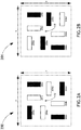
- FIGS. 1A through 2B illustrate typical overlay targets of the prior art.
- FIGS. 1A and 1B illustrate overlay targets having 180 degree and 90 degree rotational symmetry, respectively, about a center of symmetry.
- the target structures of FIG. 1A and 1B include pattern elements (e.g., 102a through 108b), which are individually invariant to 90 degree rotation. Due to the 90 degree invariance of the individual pattern elements the pattern elements of targets 100 and 101 of FIGS. 1A and 1 Bare suitable for both X-overlay and Y-overlay measurements.
- FIGS. 2A and 2B illustrate targets 200 and 201 which display invariance to a 90 degree and 180 degree rotation, respectively.
- the pattern elements e.g., 202a through 208d
- the pattern elements 202a, 204a, 202d, and 204d may be used to measure overlay in a first direction
- elements 202b, 204b, 204c, and 202c may be used to measure overlay in a second direction orthogonal to the first direction.
- US2007076205 discloses a technique for obtaining overlay error and PPE error information from a single measurement structure. This is accomplished by forming periodic sub-structures in at least two different device layers in a single measurement structure, wherein at least one segmented and one non-segmented portion is provided in the two different device layers.
- US 5952241 describes a semiconductor wafer polishing method comprises forming at least one alignment mark within an alignment area on a semiconductor wafer, forming a layer to be polished over the wafer, the layer being formed to be generally elevationally higher proximately about and surrounding the alignment area than within the alignment area, and polishing the layer US7608468 discloses a target overlay structure comprising a plurality of target structures sharing a common center of symmetry, and dummy fill in a periodic grating structure.
- a first aspect of the present invention provides a system as recited in claim 1.
- an overlay target suitable for imaging based overlay metrology is described in accordance with the present disclosure.
- the overlay targets of the present invention may be used to determine overlay error between two successive process layers of a semiconductor wafer.
- an overlay target may be utilized to measure the alignment of a first semiconductor layer with respect to a second semiconductor layer, where the second layer and the first layer are disposed successively.
- an overlay target may be used to determine alignment error between two structures formed on a common semiconductor layer via two or more different processes (e.g., lithographic exposures).
- an overlay target may be utilized to measure the alignment of a first pattern with respect to a second pattern, where the first pattern and the second pattern are successive patterns formed on the same semiconductor layer.
- an overlay target may be printed at a specific location on a first wafer layer and a second wafer layer, so that when the first and second layers are properly aligned the pattern elements of the first structure and second structure of the overlay target also align.
- first and second layers are 'mis-registered,' however, a relative shift between the pattern elements of the first structure 102 and the second structure 104 of a given thin overlay mark 100 exists, a shift that can be measured through a variety of techniques.
- the structures and pattern elements described herein may be fabricated using any process known in the art suitable for semiconductor wafer processing, such as, but not limited to, photolithographic, etching, and deposition techniques. Methods for printing overlay targets and their contained structures, pattern elements, and pattern sub-elements are described generally in U.S. application Ser. No. 11/179,819 filed on Feb. 23.
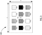
- FIG. 3 illustrates a top plan view of a six-layer overlay target 300 suitable for imaging based metrology.
- the overlay target 300 may include three or more target structures.
- each of the target structures of the overlay target 300 includes two or more pattern elements.
- texture patterns in FIG.2 are used to represent the different target structures of a target, wherein pattern elements belonging to the same target structure have the same texture.
- the texture patterns displayed in the various figures of the present disclosure should not be interpreted as limiting as the selected texture pattern is not representative of a structural aspect of the associated pattern element, but is merely utilized to represent pattern elements of the same target structure.
- FIG. 2 illustrates a top plan view of a six-layer overlay target 300 suitable for imaging based metrology.
- the overlay target 300 may include three or more target structures.
- each of the target structures of the overlay target 300 includes two or more pattern elements.
- texture patterns in FIG.2 are used to represent the different target structures of a target, wherein pattern elements belonging to the same target structure have the same texture.
- the target 300 may include six target structures (each structure illustrated with a unique texture). Further, each of the six target structures of target 300 may include two pattern elements. For instance, as shown in FIG. 3 , a first structure may include pattern elements 302a and 302b, a second structure may contain pattern elements 304a and 304b, a third structure may include pattern elements 306a and 306b, a fourth structure may include pattern elements 308a and 308b, a fifth structure may include pattern elements 310a and 310b, and a sixth structure may include pattern elements 312a and 312b. More generally, a given structure of target 300 (i.e., first, second, third, or up to an Nth structure) may contain from two pattern elements up to and including an Nth pattern element.
- each of the target structures of target 300 are designed such that each is invariant to a 180 degree rotation about a common center of symmetry 110.
- the top view image of the structures remains identical to the top view image of the structures prior to rotation.
- the overall target consisting of the multiple individual structures, is invariant to a 180 degree rotation about the common center of symmetry 110 when properly aligned.
- the two pattern elements of each structure may be oriented at positions diagonally opposed to one another, resulting in 180 degree rotational symmetry for the overlay target as a whole.
- overlay metrology measurements may be performed utilizing any pair of the six target structures present in overlay target 300.
- overlay metrology measurements may be acquired from all six structures in a single image grab.
- first structure and a second structure share a common center of symmetry by design when a first layer and a second layer are properly aligned, upon misalignment between a first layer and a second layer, the first structure and the second structure shift with respect to one another.
- the center of symmetry of a first structure and the center of symmetry of a second structure will shift and the center of symmetries of the first structure and the second structure will no longer coincide.
- this concept may be extended to all of the structures within a given target of the present invention. It is the measurement of this shift between centers of symmetries of various structures of a target 300 which enables the overlay measurement. Measurement techniques that may be used in the context of the target 200 described herein are described in U.S. applications Ser. No. 11/830,782 filed on Jul. 30, 2007 , and Ser. No. 11/179,819 filed on Jul. 11, 2005 .
- each pattern element of each structure of the target 300 possesses an individual center of symmetry.
- the pattern elements of 300 are designed such that each pattern element (e.g., 302a-302b, 304a-304b and etc.) are invariant to a 90° rotation about the center of symmetry of the individual pattern element.
- X-overlay and Y-overlay measurements may be performed utilizing the same pattern element.
- a rectangular target region as depicted in FIG. 3 , is not a limitation and that generally a variety of mark region shapes (e.g., square, trapezoid, parallelogram, or ellipse) may be used to characterize the perimeter of an overlay target boundary.
- mark region shapes e.g., square, trapezoid, parallelogram, or ellipse
- a set of structures of a given target may be arranged such that their outermost edges form an ellipsoidal or circular shaped target region.
- the two dimensional shapes of the various pattern elements of the first structure and the second structure are not limited.
- the square shape of the pattern elements as depicted in FIG. 3 , should not be interpreted as a limitation but merely an illustration. It is recognized that a variety of pattern element shapes exist that may produce the 90 degree rotational invariance as required of the pattern elements (e.g., 302a through 312b) of target structure 300.
- the pattern elements of target structure 300 may include pattern elements having a square shape, a cross shape, or a diamond shape, among others.
- the pattern elements of the first structure may be identical to the pattern elements of the second structure.
- all of the pattern elements of target structure 300 may have a square shape.
- the pattern elements of the various structures of the target structure 300 may be different.
- the pattern elements 302a and 302b of the first structure may be different from the pattern elements 304a and 304b of the second structure.
- the pattern elements 302a and 302b of the first structure may have a square shape
- the pattern elements 304a and 304b of the second structure may have a 'cross' shape (not shown).
- the shapes of the pattern elements within a single target structure may be uniform. More specifically, the pattern elements within a given structure may have an identical shape. For example, the pattern elements 306a and 306b of the third target structure may both have a square shape.
- the shapes of the pattern elements within a given structure may be non-uniform (not shown). More specifically, a given structure may contain more than one pattern element shape.
- the fourth structure may include pattern element 308a having a 'cross' shape (not shown) and a pattern element 308b having a square shape. It should be recognized that there is no generalized limitation on the shape of the pattern elements of the target structures of overlay target 300, provided the shapes of the pattern elements and the orientation of the pattern elements results in the target structures having 180 degree rotational invariance about their common center of symmetry and each pattern element of each target structure having 90 degree rotational invariance about its individual center of symmetry.
- the pattern elements of the structures of overlay target 300 may be arranged according to various sets of spatial positions.
- the pattern elements 302a and 302b of the first structure, the pattern elements 304a and 304b of the second structure, the pattern elements 306a and 306b of the third structure, the pattern elements 308a and 308b of the fourth structure, the pattern elements 310a and 310b of the fifth structure, and the pattern elements 312a and 312b of the sixth structure may be arranged such that they form a periodic or non-periodic pattern.
- the two-dimensional arrangement of the pattern elements 302a through 312b forms a two-dimensional periodic array. It is contemplated herein that a variety of arrangements may be suitable for creating the 180 degree rotational invariance of the target 300.
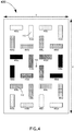
- FIG. 4 illustrates a top plan view of an overlay target 400, in accordance with an alternate illustrative example. Applicant notes that unless otherwise noted the descriptive material provided above with respect to target 300 should be interpreted to apply to the remainder of the instant disclosure.
- the multilayer overlay target 400 may include three or more target structures, with each target structure including two or more pattern elements.
- the overlay target 400 may include six target structures, with each target structure containing four pattern elements.
- a first structure may include pattern elements 402a, 402b, 402c and 402d
- a second structure may contain pattern elements 404a, 404b, 404c, and 404d
- a third structure may contain pattern elements 406a, 406b, 406c, and 406d, and so on.
- a given structure of target 400 i.e., first, second, third, or up to an Nth structure
- each of the target structures of target 400 are designed such that each is invariant to a 180 degree rotation about a common center of symmetry 110, resulting target 400 also being invariant to a 180 degree rotation.
- the pattern elements 402a and 402b of the first structure of target 400 are oriented diagonally from the pattern elements 402c and 402d and arranged such that the first target structure is invariant to 180 degree rotation about its center of symmetry 110. It is noted, however, that the target structures of target 400 are not invariant to a 90 degree rotation
- target 400 may also be utilized in overlay metrology between more than two layers. Resultantly, overlay metrology measurements may be performed utilizing any pair of the six target structures present in overlay target 400. Moreover, due to the collocation of the center of symmetries 110 of each structure of target 400, overlay metrology measurements may be acquired from all six structures in a single image grab.
- the center of symmetry for the set of pattern elements utilized for X-overlay measurements (e.g., 402a and 402d) is collocated with the set of pattern elements utilized for Y-overlay measurements (e.g., 402b and 402c).
- a design such as this allows for the simultaneous acquisition of X-overlay and Y-overlay data in a single "image grab.” As such, the move-acquire-measurement time as compared to traditional overlay targets is greatly reduced.
- the design depicted in FIG. 4 may allow for compatibility with presently existing metrology tool procedures and architectures.
- the individual pattern elements of target 400 are designed such that each pattern element (e.g., 402a-402b, 404a-404b and etc.) is invariant to a 180° rotation about the center of symmetry 112 of the individual pattern element.
- each pattern element e.g., 402a-402b, 404a-404b and etc.
- the individual pattern elements of target 400 are not invariant to a 90° rotation about the center of symmetry 112 of the individual pattern element.
- a single pattern element e.g., 402a
- each individual pattern element may be utilized to measure either X-overlay or Y-overlay.
- the target structures of target 400 include pairs of pattern elements, one designated for X-overlay and one designated for Y-overlay.
- the shapes of the pattern elements depicted in FIG. 4 do not represent a limitation as it should be recognized that there exist a number of other pattern elements shapes having 180 degree rotational symmetry (but not 90 degree rotational symmetry) which are suitable for implementation in the present invention.
- any pattern element and target structure scheme which produces 180 degree rotational symmetry (without producing 90 degree rotational symmetry) for the target structures about the common center of symmetry 110, while producing 180 degree rotational symmetry (without producing 90 degree rotational symmetry) for the individual pattern elements (e.g., 402a through 412d) about each pattern element center of symmetry 112, may be suitable for implementation in the present invention.
- the target structure and pattern element scheme depicted in FIG. 4 should be interpreted merely as illustrative and should not be considered limiting.
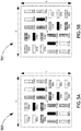
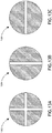
- FIG. 5A illustrates a top plan view of an overlay target 500, in accordance with an alternate illustrative example
- the multilayer target 500 may include three or more target structures, with each target structure including two or more pattern elements.
- the overlay target 500 may include six target structures, with each target structure containing four pattern elements.
- a first structure may include pattern elements 502a, 502b, 502c and 502d
- a second structure may contain pattern elements 504a, 504b, 504c, and 504d, and so on.
- a given structure of target 500 i.e., first, second, third, or up to an Nth structure
- each of the target structures of target 500 are designed such that each is invariant to a 90 degree rotation about a common center of symmetry 110, resulting in target 500 also being invariant to a 90 degree rotation.
- the pattern elements 512a, 512b, 512c, and 512d of the sixth target structure of target 500 are arranged such that the sixth target structure is invariant to 90 degree rotation about its center of symmetry 110.
- the individual pattern elements of target 500 are designed such that each pattern element (e.g., 502a-502d, 504a-504d and etc.) is invariant to a 180° rotation about the center of symmetry of the individual pattern element 112. Again, the pattern elements of 500 are not invariant to a 90° rotation about the center of symmetry of the individual pattern element 112. Therefore, as in target 400, a single pattern element (e.g., 502a) cannot be utilized to measure both X-overlay and Y-overlay. As such, each individual pattern element may be utilized to measure either X-overlay or Y-overlay.
- each pattern element may be utilized to measure either X-overlay or Y-overlay.
- the target structures of target 500 include two pairs of pattern elements, one pair (502a and 502c) designated for X-overlay measurement and one pair (502b and 502d) designated for Y-overlay measurement.
- the shapes of the pattern elements depicted in FIG. 5 do not represent a limitation as it should be recognized that there exist a number of other pattern elements shapes having 180 degree rotational symmetry (without producing 90 degree rotational symmetry) about an individual center of symmetry of the pattern element which are suitable for implementation in the present invention.
- any pattern element and target structure scheme which produces 90 degree rotational symmetry for the target structures about the common center of symmetry 110, while producing 180 degree rotational symmetry (without producing 90 degree rotational symmetry) for the individual pattern elements (e.g., 502a through 512d) about each pattern element center of symmetry 112, may be suitable for implementation in the present invention.
- the target structure and pattern element scheme depicted in FIG. 5 should be interpreted merely as illustrative and should not be considered limiting.
- FIG. 5B illustrates a top plan view of an overlay target 501, in accordance with an alternate illustrative example.
- the multilayer target 501 may include three or more target structures, with each target structure including two or more pattern elements.
- the overlay target 501 may include six target structures, with each target structure containing four pattern elements.
- a first structure may include pattern elements 514a, 514b, 514c and 514d
- a second structure may contain pattern elements 516a, 516b, 516c, and 516d
- a third structure may contain pattern elements 518a, 518b, 518c, and 518d, and so on.
- a given structure of target 501 i.e., first, second, third, or up to an Nth structure
- the overlay target 501 is designed to be invariant to 180 degrees, but not invariant to 90 degrees.
- each of the target structures of target 501 are designed such that each is at least invariant to 180 degree rotation about a common center of symmetry 110, resulting in target 501 also being invariant to a 180 degree rotation.
- the pattern elements 524a, 524b, 524c, and 524d of the sixth target structure of target 501 are arranged such that the sixth target structure is invariant to 180 degree rotation (but not 90 degree rotation) about its center of symmetry 110.
- each constituent target structure of overlay target 501 need not be limited to 180 degree rotational symmetry.
- the arrangement of pattern elements 518a, 518b, 518c, and 518d form a 90 degree rotationally invariant target structure.
- the combination of the six target structures form an overlay target 501 which lacks 90 degree rotational symmetry but possesses 180 degree rotational symmetry since the remaining target structures lack 90 degree rotational symmetry.
- any pattern element and target structure scheme which produces 180 degree rotational symmetry for the target structures about the common center of symmetry 110, while producing 180 degree rotational symmetry for the individual pattern elements (e.g., 514a through 524d) about each pattern element center of symmetry 112, may be suitable for implementation in the present invention.
- the target structure and pattern element scheme depicted in FIG. 5B should be interpreted merely as illustrative and should not be considered limiting.
- FIG. 6 illustrates a top plan view of overlay target 600, in accordance with an alternate illustrative example.
- one or more target structures of the various embodiments of the overlay targets described previously herein may lack sufficient contrast suitable for implementation in an overlay metrology measurement process.
- one or more target structures of a given overlay target 600 may be enhanced by increasing the overall target structure surface area, thereby increasing the information content of the enhanced target structure.
- the number of pattern elements included in a given target structure may be determined by the level of contrast of the given target structure.
- the first structure of target 600 may have lower contrast levels than desirable.
- the designer of the target may enhance the contrast by including additional pattern elements to the target structure.
- the first target structure of target 600 includes four overall pattern elements 602a, 602b, 602c, and 602d, as opposed to the only two pattern elements in the remaining targets structures of the target 600.
- the additional pattern elements utilized to increase contrast of a given target structure should be designed to adhere to the overall set of design rules for the given target. As such, the additional pattern elements should adhere to the symmetry requirements placed on the overall target structure and individual pattern elements in a manner consistent with the above described targets 300, 400, 500, and 501.
- the pattern elements 602a, 602b, 602c, and 602d maintain 180 degree rotational symmetry about the center of symmetry 110 of the overall target 600. Resultantly, the target 600 will maintain 180 degree rotational symmetry about the center of symmetry 110 in a manner similar to targets 300, 400, and 501 described previously herein. Furthermore, also as illustrated in FIG. 6 , the pattern elements 602a, 602b, 602c, and 602d maintain 90 degree rotational symmetry about the center of symmetry of the individual pattern elements in a manner consistent with target 200 described previously herein.
- FIG. 7 illustrates a top plan view of overlay target 700, in accordance with an alternate illustrative example.
- each target structure of target 700 may include the number of pattern elements necessary to achieve adequate levels of information content (i.e., contrast).
- the information content of one or more target structures may be satisfied by increasing the overall target structure area of target structures lacking in contrast.
- the first structure, second structure, third structure and fourth structure of target 700 may have varying degrees of information deficiencies. As such, the designer may tailor the number of pattern elements of each target structure to make up for this deficiency.
- the first structure having the lowest level of contrast, may include twelve pattern elements 702a, 702b, 702c, 702d, 702e, 702f, 702g, 702h, 702i, 702j, 702k, and 702l.
- the second and third structures may have a similar level of contrast needs, each including eight overall pattern elements.
- the second structure includes 704a, 704b, 704c, 704d, 704e, 704f, 704g, and 704h, while the third structure includes 706a, 706b, 706c, and 706d.
- the fourth target structure of target 700 may require little contrast enhancement or may have surplus information content.
- the fourth target structure may include only 4 target pattern elements 708a, 708b, 708c, and 708d.
- the additional pattern elements utilized to increase contrast of the target structures of overlay target 700 should be designed to adhere to the overall set of design rules for the given target. As such, the additional pattern elements should adhere to the symmetry requirements placed on the overall target structure and individual pattern elements in a manner consistent with the above described targets 400, 500, and 501.
- the pattern elements 704a...704h of the second target structure maintain 90 degree rotational symmetry about the center of symmetry 110 of the overall target 700, while pattern elements 708a ... 708d of the fourth target structure possess 180 degree rotational symmetry about the center of symmetry 110.
- the target 700 will maintain at least 180 degree rotational symmetry about the center of symmetry 110 in a manner similar to targets 400 and 501 described previously herein. It is further recognized that the above described utilization of additional pattern elements may also be implemented such that the overlay target possesses 90 degree rotational symmetry similar to target 500 illustrated in FIG. 5A .
- the individual pattern elements 702a ... 702l, 704a ... 704h, 706a ... 706h, and 708a ... 708d each are 180 degree rotationally symmetric about the center of symmetry of each individual pattern element in a manner consistent with target 400, 500, and 501 described previously herein.
- FIG. 8 illustrates a top plan view of overlay target 800 in the presence of dummy fill 801, in accordance with the present invention.
- the overlay targets 400, 500, and 501 wherein X-overlay and Y-overlay measurements are performed utilizing different pattern elements, allow for overlay metrology measurement processes in the presence of dummy fill 801.
- FIG. 8 depicts an overlay target 800 implemented in the presence of dummy fill 801.
- overlay target 800 includes six target structures, with each target structure including four pattern elements. In this manner, the first structure includes pattern elements 802a ... 802d, the second structure includes pattern elements 804a ... 804d, the third structure includes pattern elements 806a ... 806d, the fourth structure includes pattern elements 808a ...
- the fifth structure includes pattern elements 810a ... 810d
- the sixth structure includes pattern elements 812a ... 812d.
- two of the pattern elements of each structure are designated for X-overlay measurement (e.g., 802a, 806a, or 810a), while the remaining two pattern elements of each target structure are designated for Y-overlay measurement (e.g., 812d, 808d, or 804d).
- the pattern elements (e.g., 802a ... 812d) of target 800 each include a plurality of sub-elements 803.
- each pattern element e.g., 802a ... 812d
- the dummy fill 801 consists of a periodic grating structure printed above or below the overlay target 800 as illustrated by the FIG. 8 .
- each pattern element e.g., 802a ... 812d
- the sub-elements 803 of each pattern element (e.g., 802a ... 812d) of each structure may be aligned orthogonally with the grating structure of the dummy fill 801 structure.
- the lines of the dummy fill 801 run perpendicularly to the lines of the sub-element 803 structure. Applicant notes that by aligning the sub-elements 803 of the pattern elements (e.g., 802a ... 812d) orthogonally to the dummy fill structure 801 mitigates the risk of contamination of the metrology signal of a given overlay target with information from the underlying dummy fill structure 801.
- the overlay target 800 possesses 180 degree rotational symmetry about the common center of symmetry of the constituent target structures of the target, while the individual pattern elements (e.g., 802a ... 812d) of the target 800 possess 180 degree rotational symmetric about the center of symmetry of each individual pattern element.
- the periodicity of the sub-elements 803 of the pattern elements may consist of a resolution below that which is suitable for the implementing metrology system.
- the 1 st and -1 st diffraction orders may fall outside the aperture of the objective of the imaging system of the metrology system. It is recognized herein that this feature is particularly advantageous in the case of the dummy fill structure as it further mitigates the risk of contamination of the metrology signal of the target 800 with a signal from the dummy fill pattern 801.
- FIG. 9 illustrates a top plan view of overlay target 900 in the presence of dummy fill 801, in accordance with an alternate embodiment of the present invention.
- Target 900 is similar to target 800 in that it possesses identical symmetry requirements as well as orthogonal pattern element and dummy fill alignment.
- Target 900 illustrates a square dimensioned target suitable for implementation in a metrology process.
- FIG. 10 illustrates a top plan view of overlay target 1000 in the presence of dummy fill 801, in accordance with an alternate embodiment of the present invention.
- Target 1000 is similar to target 800 in that it possesses identical symmetry requirements as well as orthogonal pattern element and dummy fill alignment.
- Target 1000 illustrates the implementation of contrast enhancement as described previously herein with respect to FIGS. 6 and 7 .
- FIG. 10 illustrates an acquisition mark 1001 located at the center of the overlay target 1000.
- the acquisition mark 1001 may be utilized to identify the approximate position of the center of the target in order to position the target in the center of the field of view (FOV) of the given metrology tool.
- FOV field of view
- systems 1100 and 1200 suitable for contrast enhancement are described in accordance with the present invention. It is contemplated herein that systems 1100 and 1200 of the present invention may enable the implementation of the various multi-layer targets described previously herein.
- One limitation associated with the multilayer targets of the present invention includes the potential for lack of information content (i.e., contrast level) associated with their small measurement structures.
- the systems 1100 and 1200 are directed at providing enhanced contrast levels to counteract the presence of low contrast in one or more target structures of the various multi-layer targets of the present invention.
- the system 1100 is directed at the utilization of structured illumination in order to enhance the contrast level associated with one or more measurement structures associated with the target structures of the multilayer targets of the present invention.
- the system 1200 is directed at the utilization of cross-polarization in order to enhance the contrast level associated with one or more measurement structures associated with the target structures of the multi-layer targets of the present invention.
- the systems 1100 and 1200 of the present invention may consist (but not required to consist) of adapting or reconfiguring presently existing optical metrology systems.
- the present invention may consist of adapting the KLA-Tencor Archer 100 overlay control system.
- a first linear polarizer may be inserted into an illumination path of a traditional system (e.g., Archer 100 system), while a second linear polarizer is placed within the imaging path of the traditional system.
- an aperture may be inserted at a pupil plane of an illumination path of a traditional system (e.g., Archer 100 system).
- the present invention is not limited to an adaptation of an Archer 100 system, but rather the description above should be interpreted merely as an illustration. It is anticipated that the present invention may be extended to a wide variety of microscopy and overlay metrology systems.
- the system 1100 suitable for contrast enhancement of a multi-layer overlay metrology target may include an illumination source 1102, an aperture 1104, a beam splitter 1108, and a detector 1110 configured to receive light reflected from one or more specimens 1114 (e.g., one or more wafers of a wafer lot).
- an illumination source 1102 an aperture 1104, a beam splitter 1108, and a detector 1110 configured to receive light reflected from one or more specimens 1114 (e.g., one or more wafers of a wafer lot).
- the illumination source 1102 of the system 1100 may include any illumination source known in the art.
- the illumination source 1102 may include a broadband light source (e.g., white light source).
- the illumination source 1102 may include, but is not limited to, a halogen light source (HLS).
- the halogen light source may include, but is not limited to, a tungsten based halogen lamp.
- the illumination source 1102 may include a Xenon arc lamp.
- the beam splitter 1108 of the system 1100 may split the light beam emanating from an illumination source 1102, after passing through the aperture, into two paths: an object path 1112 and a reference path 1113.
- the object path 1112 and the reference path 113 of the system 100 may form a portion of a two beam interference optical system.
- the beam splitter 1108 may direct a first portion of the beam of light from the illumination path 1115 along the object path 1112, while allowing a second portion of the beam of light from the illumination path 115 to be transmitted along the reference path 1113.
- the beam splitter 108 may direct a portion of the light emanating from the illumination source 1102, after passing through the aperture 1104, to the surface of the specimen 1114 (e.g., via object path 1112) disposed on the specimen stage 1118.
- the beam splitter 1108 may transmit a second portion of the light emanating from the illumination source 1102 to the components of the reference path 1113.
- the beam splitter 1108 may transmit a portion of light from the illumination path 1115 along the reference path 1113 to a reference mirror (not shown). It should be recognized by those skilled in the art that any beam splitter known in the art is suitable for implementation as the 1 beam splitter 1108 of the present invention.
- the reference path 1113 may include, but is not limited to, a reference mirror, a reference objective, and a shutter configured to selectively block the reference path 1113.
- a two-beam interference optical system may be configured as a Linnik interferometer. Linnik interferometry is described generally in U.S. Patent No. 4,818,110, issued on April 4, 1989 , and U.S. Patent No. 6,172,349, issued on January 9, 2001 .
- the system 1100 may include a main objective lens 1109.
- the main objective lens 1109 may aid in directing light along the object path 1112 to the surface of the specimen 1114 disposed on the specimen stage 1118.
- the beam splitter 1108 may direct a portion of the light beam 1115 emanating from the illumination source 1102, after passing through the aperture 1104, along the object path 1112.
- the main objective lens 1109 may focus light from the object path 1112, which is collinear with the primary optical axis 1107, onto the surface of the specimen 1114.
- any objective lens known in the art may be suitable for implementation as the main objective lens 1109 of the present invention.
- a portion of the light impinging on the surface of the specimen 1114 may be reflected by the specimen 1114 and directed along the primary optical axis 1107 via the objective 1109 and the beam splitter 1108 toward the detector 1110.
- intermediate optics devices such as intermediate lenses, additional beam splitters (e.g., a beam splitter configured to split off a portion of light to a focusing system), and imaging lenses 1106 may be placed between the objective 1109 and the imaging plane of the detector 1110.
- the detector 1110 of the system 100 may be disposed along the primary optical axis 1107 of the system 1100.
- the camera 1110 may be arranged to collect imagery data from the surface of the specimen 1114.
- the detector 1110 may include a charge coupled device (CCD) based camera system.
- the detector 1110 may include a time delay integration (TDI)-CCD based camera system.
- the detector 1110 may be communicatively coupled with a computer system (not shown).
- digitized imagery data may be transmitted from the detector 1110 to the computer system via a signal, such as a wireline signal (e.g., copper line, fiber optic cable, and the like) or a wireless signal (e.g., wireless RF signal).
- a signal such as a wireline signal (e.g., copper line, fiber optic cable, and the like) or a wireless signal (e.g., wireless RF signal).
- the detector 110 may reside along an additional optical axis of the system 1100.
- one or more additional beam splitters may be utilized to divert a portion of light reflected from the surface of the specimen 1114 and traveling along the object path 1112 onto an additional optical axis, which non-parallel to the object path 1112.
- the camera 1110 may be arranged such that light traveling along the additional optical axis impinges the image plane of the camera 1110.
- the aperture 1104 may be position at a pupil plane of the illumination path 1115.
- the aperture 1104 may be configured to have a well-defined shape in order to select an predetermined illumination angle of the illumination emanating from the illumination source 1102. The illumination angle is selected so as to achieve a selected contrast level at an imaging plane of the detector 1110.
- the aperture may have a geometric shape or a combination of geometric shapes.
- the aperture may have an 'X' shape or a 'cross' shape.
- the aperture may have a ring shape. It is further recognized herein that these shapes may be achieved via diffractive optical elements.
- the illumination path may include a plurality of apertures.
- one of the plurality of apertures may be selected during recipe training in order to optimize the contrast level for a specific stack and target design. It is recognized herein that this may be done utilizing a trial and error method.
- the aperture 1104 may include a tunable aperture.
- the aperture 1104 may consist of a tunable aperture that may be programmed by a user in order to produce a plurality of selectable illumination structures.
- a programmed tunable aperture may be tuned in a manner to optimize the contrast for a specific stack or target design.
- the tunable aperture may include, but is not limited to, a micro mirror array.
- the system 1200 suitable for contrast enhancement of a multi-layer overlay metrology target may include an illumination source 1202, a first polarizer 1204, a beam splitter 1206, a second polarizer 1208 and a detector 1210 configured to receive light reflected from one or more specimens 1212 (e.g., one or more wafers of a wafer lot).
- an illumination source 1202 a first polarizer 1204, a beam splitter 1206, a second polarizer 1208 and a detector 1210 configured to receive light reflected from one or more specimens 1212 (e.g., one or more wafers of a wafer lot).
- the illumination source 1202, the beam splitter 1206, the detector of 1210, the specimen stage 1214, and the reference path 1216 are similar to the illumination source 1102, the beam splitter 1108, the detector of 1110, the specimen stage 1118, and the reference path of 1113 of system 1100.
- the description of system 1100 should be interpreted to extend to system 1200 except where otherwise noted.
- the first polarizer 1204 is arranged to polarize light emanating from the illumination source 1202.
- the first 1204 may be disposed along an illumination path 1205 such that light emanating from the illumination source 1202 may be polarized by the first polarizer 1204.
- the second polarizer 1208 may be arranged to serve as an analyzer for light reflected from the specimen 1202.
- the first polarizer 1204 and the second polarizer 1208 may configured be such that the amount of light reflected from unpatterned parts of the specimen 1212 or from periodic unresolved patterns of the specimen 1212 that reaches the imaging plane of the detector 1210 is minimized.
- the first polarizer 1204 and the second polarizer 1208 may both include linear polarizers. In the case of linear polarizers, the first polarizer 1204 and the second polarizer 1208 may be arranged such that their polarizing axes are substantially perpendicular to one another.
- the first polarizer 1204 may include a polarizer configured to transmit only radially polarized light, while the second polarizer is configured to transmit only azimuthally polarized light.
- the signal from unpatterned portions of the specimen 1212 may be minimized in a variety of other manners.
- a combination of wave-plates and polarizers may be implemented to achieve the results illustrated above.
- a first polarizer 1204 and first quarter-wave plate (not shown) oriented at 45 degrees with respect to the first polarizer may be positioned in the illumination path 1205, while a second polarizer 1208 and a second quarter-wave plate (not shown) oriented at 45 degree with respect to the second polarizer may be positioned along the imaging path 1209.
- any combination of polarizers and wave-plates e.g., half-wave plate which creates the cross-polarization effect as described above may be suitable for implementation in the present invention.
- the systems 1100 and 1200 may be utilized in combination to improve the level of contrast.
- the present invention may be utilized to ensure a low level of intensity at a point of symmetry of the target.
- the combination of structured illumination and cross-polarization aspects of the present invention may be implemented utilizing the illumination pupils illustrated in FIG. 13 .
- a suitable illumination pupil may have a cross-shape 1302, a vertical line shape 1304 (e.g., Y-direction), or a horizontal line shape 1306 (e.g., X-direction).
- the illumination pupils 1302, 1304, and 1306 may be implemented in combination with an illumination polarizer and an imaging polarizer.
- the pupils 1302-1306 may be implemented in concert with a X-polarizer disposed within the illumination path (e.g., 1115 or 1205) of the system and a Y-polarizer disposed within the imaging path (e.g., 1107 or 1207) of the system.
- the pupils 1302-1306 may be implement in concert with a Y-polarizer disposed within the illumination path of the system and a X-polarizer disposed within the imaging path of the system.
- All of the system and methods described herein may include storing results of one or more steps of the method embodiments in a storage medium.
- the results may include any of the results described herein and may be stored in any manner known in the art.
- the storage medium may include any storage medium described herein or any other suitable storage medium known in the art.
- the results can be accessed in the storage medium and used by any of the method or system embodiments described herein, formatted for display to a user, used by another software module, method, or system, etc.
- the results may be stored "permanently,” “semi-permanently,” temporarily, or for some period of time.
- the storage medium may be random access memory (RAM), and the results may not necessarily persist indefinitely in the storage medium.
- a typical data processing system generally includes one or more of a system unit housing, a video display device, a memory such as volatile and non-volatile memory, processors such as microprocessors and digital signal processors, computational entities such as operating systems, drivers, graphical user interfaces, and applications programs, one or more interaction devices, such as a touch pad or screen, and/or control systems including feedback loops and control motors (e.g., feedback for sensing position and/or velocity; control motors for moving and/or adjusting components and/or quantities).
- a typical data processing system may be implemented utilizing any suitable commercially available components, such as those typically found in data computing/communication and/or network computing/communication systems.
- any two components herein combined to achieve a particular functionality can be seen as “associated with” each other such that the desired functionality is achieved, irrespective of architectures or intermedial components.
- any two components so associated can also be viewed as being “connected”, or “coupled”, to each other to achieve the desired functionality, and any two components capable of being so associated can also be viewed as being “couplable”, to each other to achieve the desired functionality.
- couplable examples include but are not limited to physically mateable and/or physically interacting components and/or wirelessly interactable and/or wirelessly interacting components and/or logically interacting and/or logically interactable components.
- the scope of the invention should be limited only by the claims appended hereto.
Priority Applications (1)
| Application Number | Priority Date | Filing Date | Title |
|---|---|---|---|
| EP21186660.3A EP3916758A1 (en) | 2010-08-03 | 2011-07-28 | Multi-layer overlay metrology target and complimentary overlay metrology measurement systems |
Applications Claiming Priority (3)
| Application Number | Priority Date | Filing Date | Title |
|---|---|---|---|
| US37034110P | 2010-08-03 | 2010-08-03 | |
| US13/186,144 US9927718B2 (en) | 2010-08-03 | 2011-07-19 | Multi-layer overlay metrology target and complimentary overlay metrology measurement systems |
| PCT/US2011/045778 WO2012018673A2 (en) | 2010-08-03 | 2011-07-28 | Multi-layer overlay metrology target and complimentary overlay metrology measurement systems |
Related Child Applications (2)
| Application Number | Title | Priority Date | Filing Date |
|---|---|---|---|
| EP21186660.3A Division EP3916758A1 (en) | 2010-08-03 | 2011-07-28 | Multi-layer overlay metrology target and complimentary overlay metrology measurement systems |
| EP21186660.3A Division-Into EP3916758A1 (en) | 2010-08-03 | 2011-07-28 | Multi-layer overlay metrology target and complimentary overlay metrology measurement systems |
Publications (3)
| Publication Number | Publication Date |
|---|---|
| EP2601675A2 EP2601675A2 (en) | 2013-06-12 |
| EP2601675A4 EP2601675A4 (en) | 2017-08-23 |
| EP2601675B1 true EP2601675B1 (en) | 2021-09-01 |
Family
ID=45555937
Family Applications (2)
| Application Number | Title | Priority Date | Filing Date |
|---|---|---|---|
| EP11815104.2A Active EP2601675B1 (en) | 2010-08-03 | 2011-07-28 | Multi-layer overlay metrology target and complimentary overlay metrology measurement systems |
| EP21186660.3A Pending EP3916758A1 (en) | 2010-08-03 | 2011-07-28 | Multi-layer overlay metrology target and complimentary overlay metrology measurement systems |
Family Applications After (1)
| Application Number | Title | Priority Date | Filing Date |
|---|---|---|---|
| EP21186660.3A Pending EP3916758A1 (en) | 2010-08-03 | 2011-07-28 | Multi-layer overlay metrology target and complimentary overlay metrology measurement systems |
Country Status (7)
| Country | Link |
|---|---|
| US (2) | US9927718B2 (zh) |
| EP (2) | EP2601675B1 (zh) |
| JP (3) | JP5894158B2 (zh) |
| KR (6) | KR101380532B1 (zh) |
| CN (5) | CN105589301B (zh) |
| TW (5) | TWI666529B (zh) |
| WO (1) | WO2012018673A2 (zh) |
Families Citing this family (52)
| Publication number | Priority date | Publication date | Assignee | Title |
|---|---|---|---|---|
| US10890436B2 (en) | 2011-07-19 | 2021-01-12 | Kla Corporation | Overlay targets with orthogonal underlayer dummyfill |
| US9709903B2 (en) * | 2011-11-01 | 2017-07-18 | Kla-Tencor Corporation | Overlay target geometry for measuring multiple pitches |
| SG2014008841A (en) * | 2012-05-22 | 2015-01-29 | Kla Tencor Corp | Overlay targets with orthogonal underlayer dummyfill |
| US9093458B2 (en) | 2012-09-06 | 2015-07-28 | Kla-Tencor Corporation | Device correlated metrology (DCM) for OVL with embedded SEM structure overlay targets |
| WO2014062972A1 (en) * | 2012-10-18 | 2014-04-24 | Kla-Tencor Corporation | Symmetric target design in scatterometry overlay metrology |
| US9454072B2 (en) * | 2012-11-09 | 2016-09-27 | Kla-Tencor Corporation | Method and system for providing a target design displaying high sensitivity to scanner focus change |
| US10698321B2 (en) | 2012-11-21 | 2020-06-30 | Kla-Tencor Corporation | Process compatible segmented targets and design methods |
| TWI625816B (zh) | 2013-04-10 | 2018-06-01 | 克萊譚克公司 | 在目標設計及生產中之直接自行組裝 |
| KR102066320B1 (ko) * | 2013-05-29 | 2020-01-14 | 케이엘에이 코포레이션 | 다층 타겟 설계 |
| US9885961B1 (en) | 2013-05-29 | 2018-02-06 | Kla-Tencor Corporation | Partly disappearing targets |
| CN105408721B (zh) * | 2013-06-27 | 2020-01-10 | 科磊股份有限公司 | 计量学目标的极化测量及对应的目标设计 |
| US9059102B2 (en) | 2013-08-15 | 2015-06-16 | International Business Machines Corporation | Metrology marks for unidirectional grating superposition patterning processes |
| US9257351B2 (en) | 2013-08-15 | 2016-02-09 | Globalfoundries Inc. | Metrology marks for bidirectional grating superposition patterning processes |
| US9121890B2 (en) | 2013-10-30 | 2015-09-01 | Globalfoundries Inc. | Planar metrology pad adjacent a set of fins of a fin field effect transistor device |
| KR102156408B1 (ko) | 2013-11-19 | 2020-09-16 | 삼성전자주식회사 | 레이어드 디스플레이 기법을 위한 디스플레이 장치 및 영상 생성 방법 |
| US9490182B2 (en) * | 2013-12-23 | 2016-11-08 | Kla-Tencor Corporation | Measurement of multiple patterning parameters |
| KR102119290B1 (ko) * | 2014-02-12 | 2020-06-05 | 케이엘에이 코포레이션 | 부정확도를 감소시키고 콘트라스트를 유지하는 충전 요소를 갖는 계측 타겟 |
| US9851300B1 (en) * | 2014-04-04 | 2017-12-26 | Kla-Tencor Corporation | Decreasing inaccuracy due to non-periodic effects on scatterometric signals |
| CN106462076B (zh) | 2014-06-02 | 2018-06-22 | Asml荷兰有限公司 | 设计度量目标的方法、具有度量目标的衬底、测量重叠的方法、以及器件制造方法 |
| WO2015193904A1 (en) * | 2014-06-19 | 2015-12-23 | Nova Measuring Instruments Ltd. | Test structure design for metrology measurements in patterned samples |
| KR20160007192A (ko) | 2014-07-11 | 2016-01-20 | 삼성전자주식회사 | 오버레이 측정 방법, 오버레이 측정 시스템 및 이를 이용한 반도체 장치의 제조 방법 |
| CN106575630B (zh) | 2014-07-13 | 2021-05-25 | 科磊股份有限公司 | 使用叠加及成品率关键图案的度量 |
| US10228320B1 (en) | 2014-08-08 | 2019-03-12 | KLA—Tencor Corporation | Achieving a small pattern placement error in metrology targets |
| WO2016030255A2 (en) | 2014-08-29 | 2016-03-03 | Asml Netherlands B.V. | Metrology method, target and substrate |
| KR102607646B1 (ko) * | 2015-05-19 | 2023-11-29 | 케이엘에이 코포레이션 | 오버레이 측정을 위한 지형 위상 제어 |
| US10062543B2 (en) * | 2015-06-23 | 2018-08-28 | Kla-Tencor Corp. | Determining multi-patterning step overlay error |
| CN106328629A (zh) * | 2015-06-30 | 2017-01-11 | 华邦电子股份有限公司 | 对准图形及其配置方法 |
| CN109313011A (zh) * | 2016-05-30 | 2019-02-05 | 索尼公司 | 信息处理装置、信息处理方法、程序和成像系统 |
| CN109690234B (zh) | 2016-09-15 | 2021-09-14 | 科磊股份有限公司 | 用于优化以成像为基础的覆盖度量的聚焦的系统及方法 |
| JP6319395B2 (ja) * | 2016-10-14 | 2018-05-09 | オムロン株式会社 | 3次元測定装置および3次元測定方法 |
| EP3339959A1 (en) | 2016-12-23 | 2018-06-27 | ASML Netherlands B.V. | Method of determining a position of a feature |
| FR3062516B1 (fr) * | 2017-01-30 | 2019-04-12 | Commissariat A L'energie Atomique Et Aux Energies Alternatives | Procede de mesure du desalignement entre une premiere et une seconde zones de gravure |
| KR102370347B1 (ko) * | 2017-02-02 | 2022-03-04 | 에이에스엠엘 네델란즈 비.브이. | 메트롤로지 방법 및 장치 및 연계된 컴퓨터 제품 |
| KR102432667B1 (ko) * | 2017-05-15 | 2022-08-17 | 삼성전자주식회사 | 오버레이 보정방법 및 제어 시스템 |
| EP3404488A1 (en) * | 2017-05-19 | 2018-11-21 | ASML Netherlands B.V. | Method of measuring a target, metrology apparatus, lithographic cell, and target |
| US10627720B2 (en) | 2017-08-18 | 2020-04-21 | Globalfoundries Inc. | Overlay mark structures |
| JP6848772B2 (ja) | 2017-08-31 | 2021-03-24 | 株式会社デンソー | 熱交換器 |
| US10204867B1 (en) * | 2017-08-31 | 2019-02-12 | Taiwan Semiconductor Manufacturing Co., Ltd. | Semiconductor metrology target and manufacturing method thereof |
| IL272780B2 (en) | 2017-09-22 | 2023-11-01 | Asml Netherlands Bv | A method for determining a parameter for building processes |
| US10473460B2 (en) * | 2017-12-11 | 2019-11-12 | Kla-Tencor Corporation | Overlay measurements of overlapping target structures based on symmetry of scanning electron beam signals |
| US10707175B2 (en) | 2018-05-22 | 2020-07-07 | Globalfoundries Inc. | Asymmetric overlay mark for overlay measurement |
| US11302544B2 (en) | 2019-03-28 | 2022-04-12 | Kla-Tencor Corporation | Method for measuring and correcting misregistration between layers in a semiconductor device, and misregistration targets useful therein |
| CN112838017A (zh) * | 2019-11-22 | 2021-05-25 | 长鑫存储技术有限公司 | 光刻图形检测方法及系统 |
| CN111290219B (zh) * | 2020-01-20 | 2021-03-26 | 长江存储科技有限责任公司 | 测量晶圆套刻精度的方法和设备、计算机可读存储介质 |
| EP4111495A4 (en) | 2020-04-15 | 2024-04-10 | Kla Corp | MISREGISTRATION TARGET WITH DEVICE-SCALED FEATURES FOR MEASURING MISREGISTRATION OF SEMICONDUCTOR DEVICES |
| US11676909B2 (en) * | 2020-05-05 | 2023-06-13 | Kla Corporation | Metrology targets for high topography semiconductor stacks |
| WO2021224009A1 (en) * | 2020-05-07 | 2021-11-11 | Asml Netherlands B.V. | A substrate comprising a target arrangement, and associated at least one patterning device, lithographic method and metrology method |
| US11686576B2 (en) * | 2020-06-04 | 2023-06-27 | Kla Corporation | Metrology target for one-dimensional measurement of periodic misregistration |
| CN112034677B (zh) * | 2020-09-17 | 2024-02-06 | 合肥晶合集成电路股份有限公司 | 一种套刻标记、套刻标记方法及套刻测量方法 |
| US11862524B2 (en) | 2021-06-28 | 2024-01-02 | Kla Corporation | Overlay mark design for electron beam overlay |
| WO2023136845A1 (en) * | 2022-01-13 | 2023-07-20 | Kla Corporation | Calibrated measurement of overlay error using small targets |
| KR102580204B1 (ko) * | 2023-03-02 | 2023-09-19 | (주)오로스 테크놀로지 | 1차원 오버레이 오차 측정을 위한 오버레이 마크, 이를 이용한 광학 수차 평가 방법, 이를 이용한 오버레이 마크 품질 평가 방법, 오버레이 측정 장치, 오버레이 측정 방법 및 반도체 소자의 제조방법 |
Family Cites Families (182)
| Publication number | Priority date | Publication date | Assignee | Title |
|---|---|---|---|---|
| NL7606548A (nl) | 1976-06-17 | 1977-12-20 | Philips Nv | Werkwijze en inrichting voor het uitrichten van een i.c.-patroon ten opzichte van een halfgelei- dend substraat. |
| US4166219A (en) | 1978-05-19 | 1979-08-28 | Bell Telephone Laboratories, Incorporated | Detection of ground state hydrogen and deuterium |
| US4290384A (en) | 1979-10-18 | 1981-09-22 | The Perkin-Elmer Corporation | Coating apparatus |
| US4437760A (en) | 1981-12-07 | 1984-03-20 | The Perkin-Elmer Corp. | Reusable electrical overlay measurement circuit and process |
| US4538105A (en) | 1981-12-07 | 1985-08-27 | The Perkin-Elmer Corporation | Overlay test wafer |
| US4475811A (en) | 1983-04-28 | 1984-10-09 | The Perkin-Elmer Corporation | Overlay test measurement systems |
| US4568189A (en) | 1983-09-26 | 1986-02-04 | The United States Of America As Represented By The Secretary Of The Navy | Apparatus and method for aligning a mask and wafer in the fabrication of integrated circuits |
| US4703434A (en) | 1984-04-24 | 1987-10-27 | The Perkin-Elmer Corporation | Apparatus for measuring overlay error |
| JPS61168227A (ja) | 1985-01-21 | 1986-07-29 | Mitsubishi Electric Corp | 微細パタ−ン露光用基板及び微細パタ−ン露光装置 |
| JPS61170032A (ja) | 1985-01-23 | 1986-07-31 | Sumitomo Electric Ind Ltd | 集積回路のマスク位置合せ用アライメントマ−ク |
| DE3530439A1 (de) | 1985-08-26 | 1987-02-26 | Siemens Ag | Vorrichtung zum justieren einer mit mindestens einer justiermarke versehenen maske bezueglich eines mit mindestens einer gitterstruktur versehenen halbleiterwafers |
| US4714874A (en) | 1985-11-12 | 1987-12-22 | Miles Inc. | Test strip identification and instrument calibration |
| IT1186523B (it) | 1985-12-31 | 1987-11-26 | Sgs Microelettronica Spa | Procedimento per la valutazione dei parametri di processo nella fabbricazione di dispositivi a semiconduttore |
| NL8600639A (nl) | 1986-03-12 | 1987-10-01 | Asm Lithography Bv | Werkwijze voor het ten opzichte van elkaar uitrichten van een masker en een substraat en inrichting voor het uitvoeren van de werkwijze. |
| GB2188417B (en) | 1986-03-19 | 1990-02-21 | British Steel Corp | Molten metal gas analysis |
| US4818110A (en) | 1986-05-06 | 1989-04-04 | Kla Instruments Corporation | Method and apparatus of using a two beam interference microscope for inspection of integrated circuits and the like |
| US5148214A (en) | 1986-05-09 | 1992-09-15 | Canon Kabushiki Kaisha | Alignment and exposure apparatus |
| KR900004269B1 (ko) | 1986-06-11 | 1990-06-18 | 가부시기가이샤 도시바 | 제 1물체와 제 2 물체와의 위치 맞추는 방법 및 장치 |
| US4929083A (en) | 1986-06-19 | 1990-05-29 | Xerox Corporation | Focus and overlay characterization and optimization for photolithographic exposure |
| US4757207A (en) * | 1987-03-03 | 1988-07-12 | International Business Machines Corporation | Measurement of registration of overlaid test patterns by the use of reflected light |
| US4890239A (en) | 1987-10-20 | 1989-12-26 | Shipley Company, Inc. | Lithographic process analysis and control system |
| US4855253A (en) | 1988-01-29 | 1989-08-08 | Hewlett-Packard | Test method for random defects in electronic microstructures |
| JP2831643B2 (ja) | 1988-02-23 | 1998-12-02 | 株式会社東芝 | パターン露光方法 |
| JP2666859B2 (ja) | 1988-11-25 | 1997-10-22 | 日本電気株式会社 | 目合せ用バーニヤパターンを備えた半導体装置 |
| JPH02260441A (ja) | 1989-03-30 | 1990-10-23 | Sumitomo Metal Ind Ltd | 半導体素子 |
| NL8900991A (nl) | 1989-04-20 | 1990-11-16 | Asm Lithography Bv | Apparaat voor het afbeelden van een maskerpatroon op een substraat. |
| DE4000785A1 (de) | 1990-01-12 | 1991-07-18 | Suess Kg Karl | Justiermarken fuer zwei aufeinander einzujustierende objekte |
| DE69123610T2 (de) | 1990-02-02 | 1997-04-24 | Canon Kk | Belichtungsverfahren |
| US5112129A (en) | 1990-03-02 | 1992-05-12 | Kla Instruments Corporation | Method of image enhancement for the coherence probe microscope with applications to integrated circuit metrology |
| JPH0444307A (ja) | 1990-06-12 | 1992-02-14 | Nec Corp | 半導体装置の製造方法 |
| US5216257A (en) | 1990-07-09 | 1993-06-01 | Brueck Steven R J | Method and apparatus for alignment and overlay of submicron lithographic features |
| NL9001611A (nl) | 1990-07-16 | 1992-02-17 | Asm Lithography Bv | Apparaat voor het afbeelden van een maskerpatroon op een substraat. |
| US5343292A (en) | 1990-10-19 | 1994-08-30 | University Of New Mexico | Method and apparatus for alignment of submicron lithographic features |
| JPH04234930A (ja) | 1991-01-10 | 1992-08-24 | Shimano Inc | 釣り用リール |
| DE69231715D1 (de) | 1991-03-04 | 2001-04-12 | At & T Corp | Herstellungsverfahren von integrierten Halbleiterschaltungen unter Anwendung von latenten Bildern |
| JPH05127364A (ja) | 1991-10-30 | 1993-05-25 | Nikon Corp | フオトマスク |
| US5296917A (en) | 1992-01-21 | 1994-03-22 | Mitsubishi Denki Kabushiki Kaisha | Method of monitoring accuracy with which patterns are written |
| US5617340A (en) | 1994-04-28 | 1997-04-01 | The United States Of America As Represented By The Secretary Of Commerce | Method and reference standards for measuring overlay in multilayer structures, and for calibrating imaging equipment as used in semiconductor manufacturing |
| US5383136A (en) | 1992-03-13 | 1995-01-17 | The United States Of America As Represented By The Secretary Of Commerce | Electrical test structure and method for measuring the relative locations of conducting features on an insulating substrate |
| US5857258A (en) | 1992-03-13 | 1999-01-12 | The United States Of America As Represented By The Secretary Of Commerce | Electrical test structure and method for measuring the relative locations of conductive features on an insulating substrate |
| JP2530080B2 (ja) | 1992-03-14 | 1996-09-04 | 株式会社東芝 | 半導体製造装置の評価装置およびその評価方法 |
| US5479270A (en) | 1992-05-19 | 1995-12-26 | Eastman Kodak Company | Method and apparatus for aligning depth images |
| US5403754A (en) | 1992-09-30 | 1995-04-04 | Texas Instruments Incorporated | Lithography method for direct alignment of integrated circuits multiple layers |
| US5300786A (en) | 1992-10-28 | 1994-04-05 | International Business Machines Corporation | Optical focus phase shift test pattern, monitoring system and process |
| US5438413A (en) | 1993-03-03 | 1995-08-01 | Kla Instruments Corporation | Process for measuring overlay misregistration during semiconductor wafer fabrication |
| JPH06260390A (ja) | 1993-03-05 | 1994-09-16 | Toshiba Corp | アライメント方法 |
| US5604819A (en) | 1993-03-15 | 1997-02-18 | Schlumberger Technologies Inc. | Determining offset between images of an IC |
| US5414514A (en) | 1993-06-01 | 1995-05-09 | Massachusetts Institute Of Technology | On-axis interferometric alignment of plates using the spatial phase of interference patterns |
| JP3039210B2 (ja) | 1993-08-03 | 2000-05-08 | 日本電気株式会社 | 半導体装置の製造方法 |
| US5545593A (en) | 1993-09-30 | 1996-08-13 | Texas Instruments Incorporated | Method of aligning layers in an integrated circuit device |
| KR970010666B1 (ko) * | 1993-12-27 | 1997-06-30 | 현대전자산업 주식회사 | 반도체 소자의 패턴 중첩오차 측정방법 |
| KR0168772B1 (ko) | 1994-03-10 | 1999-02-01 | 김주용 | 포토마스크 및 그를 이용한 반도체 장치 제조 방법 |
| US5699282A (en) | 1994-04-28 | 1997-12-16 | The United States Of America As Represented By The Secretary Of Commerce | Methods and test structures for measuring overlay in multilayer devices |
| DE69531854T2 (de) | 1994-08-02 | 2004-08-19 | Koninklijke Philips Electronics N.V. | Verfahren zur wiederholten abbildung eines maskenmusters auf einem substrat |
| US5477057A (en) | 1994-08-17 | 1995-12-19 | Svg Lithography Systems, Inc. | Off axis alignment system for scanning photolithography |
| US5677091A (en) | 1994-11-01 | 1997-10-14 | International Business Machines Corporation | Lithographic print bias/overlay target and applied metrology |
| KR100197191B1 (ko) | 1994-11-14 | 1999-06-15 | 모리시다 요이치 | 레지스트 패턴 형성방법 |
| US5629772A (en) | 1994-12-20 | 1997-05-13 | International Business Machines Corporation | Monitoring of minimum features on a substrate |
| US5790254A (en) | 1994-12-20 | 1998-08-04 | International Business Machines Corporation | Monitoring of minimum features on a substrate |
| JPH08233555A (ja) | 1994-12-28 | 1996-09-13 | Matsushita Electric Ind Co Ltd | レジストパターンの測定方法及びレジストパターンの測定装置 |
| US5923041A (en) | 1995-02-03 | 1999-07-13 | Us Commerce | Overlay target and measurement procedure to enable self-correction for wafer-induced tool-induced shift by imaging sensor means |
| US5702567A (en) | 1995-06-01 | 1997-12-30 | Kabushiki Kaisha Toshiba | Plurality of photolithographic alignment marks with shape, size and spacing based on circuit pattern features |
| US5596413A (en) | 1995-08-17 | 1997-01-21 | Lucent Technologies Inc. | Sub-micron through-the-lens positioning utilizing out of phase segmented gratings |
| KR0170909B1 (ko) | 1995-09-27 | 1999-03-30 | 김주용 | 반도체 소자의 오버레이 검사방법 |
| JPH09115817A (ja) | 1995-10-13 | 1997-05-02 | Nikon Corp | 露光方法及び装置 |
| US5757507A (en) | 1995-11-20 | 1998-05-26 | International Business Machines Corporation | Method of measuring bias and edge overlay error for sub-0.5 micron ground rules |
| US5712707A (en) | 1995-11-20 | 1998-01-27 | International Business Machines Corporation | Edge overlay measurement target for sub-0.5 micron ground rules |
| GB9603262D0 (en) * | 1996-02-16 | 1996-04-17 | Bio Rad Micromeasurements Ltd | Positional measurements |
| JP2842360B2 (ja) | 1996-02-28 | 1999-01-06 | 日本電気株式会社 | 半導体装置およびその製造方法 |
| JP2842362B2 (ja) | 1996-02-29 | 1999-01-06 | 日本電気株式会社 | 重ね合わせ測定方法 |
| JPH09244222A (ja) | 1996-03-08 | 1997-09-19 | Mitsubishi Electric Corp | 重ね合わせ誤差測定用レチクル、そのレチクルを用いた重ね合わせ誤差測定方法および重ね合わせ誤差測定マーク |
| KR970067585A (ko) | 1996-03-25 | 1997-10-13 | 오노 시게오 | 결상특성의 측정방법 및 투영노광방법 |
| US5805290A (en) | 1996-05-02 | 1998-09-08 | International Business Machines Corporation | Method of optical metrology of unresolved pattern arrays |
| US5701013A (en) | 1996-06-07 | 1997-12-23 | Mosel Viltelic, Inc. | Wafer metrology pattern integrating both overlay and critical dimension features for SEM or AFM measurements |
| US6023338A (en) | 1996-07-12 | 2000-02-08 | Bareket; Noah | Overlay alignment measurement of wafers |
| US5872042A (en) | 1996-08-22 | 1999-02-16 | Taiwan Semiconductor Manufacturing Company, Ltd. | Method for alignment mark regeneration |
| KR100367500B1 (ko) | 1996-10-02 | 2003-08-14 | 주식회사 하이닉스반도체 | 노광 장비의 최적 포커스 확인 방법 |
| US5731877A (en) | 1996-10-08 | 1998-03-24 | International Business Machines Corporation | Automated system utilizing self-labeled target by pitch encoding |
| KR19980030438A (ko) | 1996-10-29 | 1998-07-25 | 김영환 | 반도체 버어니어 구조 및 그것을 이용한 오버레이 정확도 측정방법 |
| US5960125A (en) | 1996-11-21 | 1999-09-28 | Cognex Corporation | Nonfeedback-based machine vision method for determining a calibration relationship between a camera and a moveable object |
| US5912983A (en) | 1997-01-24 | 1999-06-15 | Oki Electric Industry Co., Ltd | Overlay accuracy measuring method |
| JPH10213895A (ja) | 1997-01-30 | 1998-08-11 | Sony Corp | レチクルの合わせ測定用マーク |
| US5949547A (en) | 1997-02-20 | 1999-09-07 | Taiwan Semiconductor Manufacturing Company, Ltd. | System for in-line monitoring of photo processing in VLSI fabrication |
| US5902703A (en) | 1997-03-27 | 1999-05-11 | Vlsi Technology, Inc. | Method for measuring dimensional anomalies in photolithographed integrated circuits using overlay metrology, and masks therefor |
| US6172349B1 (en) | 1997-03-31 | 2001-01-09 | Kla-Tencor Corporation | Autofocusing apparatus and method for high resolution microscope system |
| US6061119A (en) | 1997-04-14 | 2000-05-09 | Nikon Corporation | Method of measuring image-forming error of projection optical system, method of manufacturing exposure apparatus, and method of manufacturing semiconductor device |
| JP3630269B2 (ja) | 1997-08-18 | 2005-03-16 | 株式会社ルネサステクノロジ | 重ね合わせマ−クおよびこの重ね合わせマークを使用した半導体装置の製造方法 |
| US5976740A (en) | 1997-08-28 | 1999-11-02 | International Business Machines Corporation | Process for controlling exposure dose or focus parameters using tone reversing pattern |
| US5953128A (en) | 1997-08-28 | 1999-09-14 | International Business Machines Corporation | Optically measurable serpentine edge tone reversed targets |
| US5965309A (en) | 1997-08-28 | 1999-10-12 | International Business Machines Corporation | Focus or exposure dose parameter control system using tone reversing patterns |
| US5952241A (en) | 1997-09-03 | 1999-09-14 | Vlsi Technology, Inc. | Method and apparatus for improving alignment for metal masking in conjuction with oxide and tungsten CMP |
| JP3580992B2 (ja) | 1997-09-18 | 2004-10-27 | 旭化成マイクロシステム株式会社 | フォトマスク |
| US5914784A (en) | 1997-09-30 | 1999-06-22 | International Business Machines Corporation | Measurement method for linewidth metrology |
| US5877861A (en) | 1997-11-14 | 1999-03-02 | International Business Machines Corporation | Method for overlay control system |
| US6160622A (en) | 1997-12-29 | 2000-12-12 | Asm Lithography, B.V. | Alignment device and lithographic apparatus comprising such a device |
| JPH11325877A (ja) | 1998-03-31 | 1999-11-26 | Siemens Ag | 測定誤差を減少させるための方法及び装置 |
| US6077756A (en) | 1998-04-24 | 2000-06-20 | Vanguard International Semiconductor | Overlay target pattern and algorithm for layer-to-layer overlay metrology for semiconductor processing |
| US5919714A (en) | 1998-05-06 | 1999-07-06 | Taiwan Semiconductor Manufacturing Company, Ltd. | Segmented box-in-box for improving back end overlay measurement |
| US6140217A (en) | 1998-07-16 | 2000-10-31 | International Business Machines Corporation | Technique for extending the limits of photolithography |
| US6128089A (en) | 1998-07-28 | 2000-10-03 | International Business Machines Corporation | Combined segmented and nonsegmented bar-in-bar targets |
| US6137578A (en) | 1998-07-28 | 2000-10-24 | International Business Machines Corporation | Segmented bar-in-bar target |
| US6061606A (en) | 1998-08-25 | 2000-05-09 | International Business Machines Corporation | Geometric phase analysis for mask alignment |
| US6020966A (en) | 1998-09-23 | 2000-02-01 | International Business Machines Corporation | Enhanced optical detection of minimum features using depolarization |
| US6037671A (en) | 1998-11-03 | 2000-03-14 | Advanced Micro Devices, Inc. | Stepper alignment mark structure for maintaining alignment integrity |
| US6460265B2 (en) | 1998-11-12 | 2002-10-08 | International Business Machines Corporation | Double-sided wafer exposure method and device |
| US6003223A (en) | 1998-11-19 | 1999-12-21 | Headway Technologies, Inc. | Common alignment target image field stitching method for step and repeat alignment in photoresist |
| US6146910A (en) | 1999-02-02 | 2000-11-14 | The United States Of America, As Represented By The Secretary Of Commerce | Target configuration and method for extraction of overlay vectors from targets having concealed features |
| TW569083B (en) | 1999-02-04 | 2004-01-01 | Asml Netherlands Bv | Lithographic projection apparatus |
| US6042976A (en) | 1999-02-05 | 2000-03-28 | Taiwan Semiconductor Manufacturing Company, Ltd. | Method of calibrating WEE exposure tool |
| US6346979B1 (en) | 1999-03-17 | 2002-02-12 | International Business Machines Corporation | Process and apparatus to adjust exposure dose in lithography systems |
| US6084679A (en) | 1999-04-02 | 2000-07-04 | Advanced Micro Devices, Inc. | Universal alignment marks for semiconductor defect capture and analysis |
| JP2000294487A (ja) | 1999-04-06 | 2000-10-20 | Matsushita Electronics Industry Corp | 半導体装置製造用重ね合わせ測定マークの配置構造 |
| US6183919B1 (en) | 1999-06-11 | 2001-02-06 | International Business Machines Corporation | Darkfield imaging for enhancing optical detection of edges and minimum features |
| US6335151B1 (en) | 1999-06-18 | 2002-01-01 | International Business Machines Corporation | Micro-surface fabrication process |
| US6405096B1 (en) | 1999-08-10 | 2002-06-11 | Advanced Micro Devices, Inc. | Method and apparatus for run-to-run controlling of overlay registration |
| US6612159B1 (en) | 1999-08-26 | 2003-09-02 | Schlumberger Technologies, Inc. | Overlay registration error measurement made simultaneously for more than two semiconductor wafer layers |
| US6350548B1 (en) | 2000-03-15 | 2002-02-26 | International Business Machines Corporation | Nested overlay measurement target |
| US6484060B1 (en) | 2000-03-24 | 2002-11-19 | Micron Technology, Inc. | Layout for measurement of overlay error |
| TW588414B (en) | 2000-06-08 | 2004-05-21 | Toshiba Corp | Alignment method, overlap inspecting method and mask |
| US6429667B1 (en) | 2000-06-19 | 2002-08-06 | International Business Machines Corporation | Electrically testable process window monitor for lithographic processing |
| US6462818B1 (en) | 2000-06-22 | 2002-10-08 | Kla-Tencor Corporation | Overlay alignment mark design |
| US6218200B1 (en) * | 2000-07-14 | 2001-04-17 | Motorola, Inc. | Multi-layer registration control for photolithography processes |
| US7317531B2 (en) | 2002-12-05 | 2008-01-08 | Kla-Tencor Technologies Corporation | Apparatus and methods for detecting overlay errors using scatterometry |
| EP1314198B1 (en) | 2000-08-30 | 2017-03-08 | KLA-Tencor Corporation | Overlay marks, methods of overlay mark design and methods of overlay measurements |
| US7541201B2 (en) | 2000-08-30 | 2009-06-02 | Kla-Tencor Technologies Corporation | Apparatus and methods for determining overlay of structures having rotational or mirror symmetry |
| US7068833B1 (en) | 2000-08-30 | 2006-06-27 | Kla-Tencor Corporation | Overlay marks, methods of overlay mark design and methods of overlay measurements |
| US6766211B1 (en) | 2000-10-03 | 2004-07-20 | International Business Machines Corporation | Structure and method for amplifying target overlay errors using the synthesized beat signal between interleaved arrays of differing periodicity |
| US6734971B2 (en) | 2000-12-08 | 2004-05-11 | Lael Instruments | Method and apparatus for self-referenced wafer stage positional error mapping |
| US6879400B2 (en) | 2000-12-11 | 2005-04-12 | International Business Machines Corporation | Single tone process window metrology target and method for lithographic processing |
| US6803995B2 (en) | 2001-01-17 | 2004-10-12 | International Business Machines Corporation | Focus control system |
| US6819426B2 (en) * | 2001-02-12 | 2004-11-16 | Therma-Wave, Inc. | Overlay alignment metrology using diffraction gratings |
| JP2003014819A (ja) | 2001-07-03 | 2003-01-15 | Matsushita Electric Ind Co Ltd | 半導体配線基板,半導体デバイス,半導体デバイスのテスト方法及びその実装方法 |
| JP4046961B2 (ja) | 2001-09-03 | 2008-02-13 | キヤノン株式会社 | 位置検出方法、位置検出装置、露光装置及び露光方法 |
| US7061615B1 (en) * | 2001-09-20 | 2006-06-13 | Nanometrics Incorporated | Spectroscopically measured overlay target |
| US6638671B2 (en) | 2001-10-15 | 2003-10-28 | International Business Machines Corporation | Combined layer-to-layer and within-layer overlay control system |
| US6975398B2 (en) | 2001-10-15 | 2005-12-13 | International Business Machines Corporation | Method for determining semiconductor overlay on groundrule devices |
| KR100809955B1 (ko) | 2001-11-27 | 2008-03-06 | 삼성전자주식회사 | 포토리소그래피 공정의 얼라인 계측방법 |
| KR100435260B1 (ko) | 2001-12-03 | 2004-06-11 | 삼성전자주식회사 | 포토리소그래피 공정의 얼라인 계측방법 |
| US6842237B2 (en) | 2001-12-28 | 2005-01-11 | International Business Machines Corporation | Phase shifted test pattern for monitoring focus and aberrations in optical projection systems |
| US20030160163A1 (en) | 2002-02-25 | 2003-08-28 | Alan Wong | Optical metrology target design for simultaneous measurement of multiple periodic structures |
| US7190823B2 (en) * | 2002-03-17 | 2007-03-13 | United Microelectronics Corp. | Overlay vernier pattern for measuring multi-layer overlay alignment accuracy and method for measuring the same |
| US6664121B2 (en) | 2002-05-20 | 2003-12-16 | Nikon Precision, Inc. | Method and apparatus for position measurement of a pattern formed by a lithographic exposure tool |
| EP1400854A3 (en) * | 2002-09-20 | 2009-07-08 | ASML Netherlands B.V. | Alignment systems and methods for lithographic systems |
| TWI227814B (en) * | 2002-09-20 | 2005-02-11 | Asml Netherlands Bv | Alignment system and methods for lithographic systems using at least two wavelengths |
| US6869739B1 (en) | 2003-01-28 | 2005-03-22 | International Business Machines Corporation | Integrated lithographic print and detection model for optical CD |
| JP2004296921A (ja) | 2003-03-27 | 2004-10-21 | Canon Inc | 位置検出装置 |
| TWI297045B (en) * | 2003-05-07 | 2008-05-21 | Microfabrica Inc | Methods and apparatus for forming multi-layer structures using adhered masks |
| US7346878B1 (en) | 2003-07-02 | 2008-03-18 | Kla-Tencor Technologies Corporation | Apparatus and methods for providing in-chip microtargets for metrology or inspection |
| US7608468B1 (en) * | 2003-07-02 | 2009-10-27 | Kla-Tencor Technologies, Corp. | Apparatus and methods for determining overlay and uses of same |
| US7230703B2 (en) | 2003-07-17 | 2007-06-12 | Tokyo Electron Limited | Apparatus and method for measuring overlay by diffraction gratings |
| US7180593B2 (en) | 2003-11-05 | 2007-02-20 | Macronix International Co., Ltd. | Overlay mark for aligning different layers on a semiconductor wafer |
| US6952886B1 (en) * | 2003-11-10 | 2005-10-11 | 1St Silicon (Malaysia) Sdn Bhd | Overlay vernier |
| US6937337B2 (en) | 2003-11-19 | 2005-08-30 | International Business Machines Corporation | Overlay target and measurement method using reference and sub-grids |
| US7042551B2 (en) | 2004-02-03 | 2006-05-09 | International Business Machines Corporation | Method of patterning process metrology based on the intrinsic focus offset |
| US7065737B2 (en) * | 2004-03-01 | 2006-06-20 | Advanced Micro Devices, Inc | Multi-layer overlay measurement and correction technique for IC manufacturing |
| US20050286052A1 (en) * | 2004-06-23 | 2005-12-29 | Kevin Huggins | Elongated features for improved alignment process integration |
| US7791727B2 (en) | 2004-08-16 | 2010-09-07 | Asml Netherlands B.V. | Method and apparatus for angular-resolved spectroscopic lithography characterization |
| US7096127B2 (en) | 2004-10-13 | 2006-08-22 | Infineon Technologies Ag | Measuring flare in semiconductor lithography |
| US7379184B2 (en) | 2004-10-18 | 2008-05-27 | Nanometrics Incorporated | Overlay measurement target |
| US7126669B2 (en) | 2004-12-27 | 2006-10-24 | Asml Netherlands B.V. | Method and system for automated process correction using model parameters, and lithographic apparatus using such method and system |
| US7556898B2 (en) * | 2005-09-01 | 2009-07-07 | Infineon Technologies Ag | Overlay target for polarized light lithography |
| US7474401B2 (en) | 2005-09-13 | 2009-01-06 | International Business Machines Corporation | Multi-layer alignment and overlay target and measurement method |
| DE102005046973B4 (de) | 2005-09-30 | 2014-01-30 | Globalfoundries Inc. | Struktur und Verfahren zum gleichzeitigen Bestimmen einer Überlagerungsgenauigkeit und eines Musteranordnungsfehlers |
| US7526749B2 (en) | 2005-10-31 | 2009-04-28 | Kla-Tencor Technologies Corporation | Methods and apparatus for designing and using micro-targets in overlay metrology |
| US7532305B2 (en) | 2006-03-28 | 2009-05-12 | Asml Netherlands B.V. | Lithographic apparatus and device manufacturing method using overlay measurement |
| US7616313B2 (en) | 2006-03-31 | 2009-11-10 | Kla-Tencor Technologies Corporation | Apparatus and methods for detecting overlay errors using scatterometry |
| KR101244914B1 (ko) | 2006-07-03 | 2013-03-18 | 삼성전자주식회사 | 디지털 촬영장치의 제어방법 및 이 방법을 채용한 디지털촬영장치 |
| US7548315B2 (en) | 2006-07-27 | 2009-06-16 | Asml Netherlands B.V. | System and method to compensate for critical dimension non-uniformity in a lithography system |
| US7671990B1 (en) | 2006-07-28 | 2010-03-02 | Kla-Tencor Technologies Corporation | Cross hatched metrology marks and associated method of use |
| TWI302341B (en) * | 2006-08-04 | 2008-10-21 | Nanya Technology Corp | Improved overlay mark |
| KR20080035345A (ko) | 2006-10-19 | 2008-04-23 | 삼성전자주식회사 | 오버레이 계측설비 및 이를 이용한 오버레이 계측방법 |
| US20080121939A1 (en) * | 2006-11-06 | 2008-05-29 | Michael Murray | Methods of automatically generating dummy fill having reduced storage size |
| US7605907B2 (en) * | 2007-03-27 | 2009-10-20 | Asml Netherlands B.V. | Method of forming a substrate for use in calibrating a metrology tool, calibration substrate and metrology tool calibration method |
| US7473502B1 (en) | 2007-08-03 | 2009-01-06 | International Business Machines Corporation | Imaging tool calibration artifact and method |
| DE102007046850B4 (de) * | 2007-09-29 | 2014-05-22 | Globalfoundries Dresden Module One Limited Liability Company & Co. Kg | Verfahren zum Bestimmen einer Überlagerungsgenauigkeit |
| US7879515B2 (en) | 2008-01-21 | 2011-02-01 | International Business Machines Corporation | Method to control semiconductor device overlay using post etch image metrology |
| CN101251724B (zh) * | 2008-03-31 | 2010-09-15 | 上海微电子装备有限公司 | 一种用于光刻装置的对准系统、对准方法和光刻装置 |
| US7684038B1 (en) | 2008-04-04 | 2010-03-23 | Kla-Tencor Corporation | Overlay metrology target |
| US9097989B2 (en) * | 2009-01-27 | 2015-08-04 | International Business Machines Corporation | Target and method for mask-to-wafer CD, pattern placement and overlay measurement and control |
| US8361683B2 (en) * | 2010-04-09 | 2013-01-29 | International Business Machines Corporation | Multi-layer chip overlay target and measurement |
| US8513822B1 (en) * | 2010-06-30 | 2013-08-20 | Kla-Tencor Corporation | Thin overlay mark for imaging based metrology |
| CN108398856B (zh) * | 2013-08-07 | 2020-10-16 | Asml荷兰有限公司 | 量测方法和设备、光刻系统和器件制造方法 |
-
2011
- 2011-07-19 US US13/186,144 patent/US9927718B2/en active Active
- 2011-07-28 WO PCT/US2011/045778 patent/WO2012018673A2/en active Application Filing
- 2011-07-28 CN CN201610141431.9A patent/CN105589301B/zh active Active
- 2011-07-28 KR KR1020137004374A patent/KR101380532B1/ko active IP Right Grant
- 2011-07-28 CN CN202110733801.9A patent/CN113391526A/zh active Pending
- 2011-07-28 CN CN201180037316.2A patent/CN103038861B/zh active Active
- 2011-07-28 EP EP11815104.2A patent/EP2601675B1/en active Active
- 2011-07-28 KR KR1020147028219A patent/KR101700435B1/ko active IP Right Grant
- 2011-07-28 KR KR1020177001918A patent/KR20170013399A/ko active Application Filing
- 2011-07-28 CN CN201811454228.2A patent/CN110045579B/zh active Active
- 2011-07-28 CN CN201610139920.0A patent/CN105759570B/zh active Active
- 2011-07-28 KR KR1020187006323A patent/KR20180026582A/ko active Application Filing
- 2011-07-28 JP JP2013523211A patent/JP5894158B2/ja active Active
- 2011-07-28 EP EP21186660.3A patent/EP3916758A1/en active Pending
- 2011-07-28 KR KR1020207011567A patent/KR102177681B1/ko active IP Right Grant
- 2011-07-28 KR KR1020137018458A patent/KR101476080B1/ko active IP Right Grant
- 2011-08-03 TW TW107112180A patent/TWI666529B/zh active
- 2011-08-03 TW TW100127637A patent/TWI429038B/zh active
- 2011-08-03 TW TW102143936A patent/TWI548047B/zh active
- 2011-08-03 TW TW106117629A patent/TWI624917B/zh active
- 2011-08-03 TW TW105121122A patent/TWI591782B/zh active
-
2016
- 2016-02-25 JP JP2016034069A patent/JP6165283B2/ja active Active
-
2017
- 2017-06-20 JP JP2017120083A patent/JP6498236B2/ja active Active
-
2018
- 2018-03-19 US US15/925,325 patent/US10527954B2/en active Active
Also Published As
Similar Documents
| Publication | Publication Date | Title |
|---|---|---|
| EP2601675B1 (en) | Multi-layer overlay metrology target and complimentary overlay metrology measurement systems | |
| US9709903B2 (en) | Overlay target geometry for measuring multiple pitches | |
| US9007585B2 (en) | Imaging overlay metrology target and complimentary overlay metrology measurement system | |
| TWI793593B (zh) | 包含目標配置之基板及相關聯之至少一個圖案化裝置、微影方法及度量衡方法 | |
| WO2022197314A1 (en) | Sub-resolution imaging target |
Legal Events
| Date | Code | Title | Description |
|---|---|---|---|
| PUAI | Public reference made under article 153(3) epc to a published international application that has entered the european phase |
Free format text: ORIGINAL CODE: 0009012 |
|
| 17P | Request for examination filed |
Effective date: 20130304 |
|
| AK | Designated contracting states |
Kind code of ref document: A2 Designated state(s): AL AT BE BG CH CY CZ DE DK EE ES FI FR GB GR HR HU IE IS IT LI LT LU LV MC MK MT NL NO PL PT RO RS SE SI SK SM TR |
|
| DAX | Request for extension of the european patent (deleted) | ||
| A4 | Supplementary search report drawn up and despatched |
Effective date: 20170726 |
|
| RIC1 | Information provided on ipc code assigned before grant |
Ipc: H01L 21/027 20060101AFI20170720BHEP |
|
| STAA | Information on the status of an ep patent application or granted ep patent |
Free format text: STATUS: EXAMINATION IS IN PROGRESS |
|
| 17Q | First examination report despatched |
Effective date: 20190118 |
|
| GRAP | Despatch of communication of intention to grant a patent |
Free format text: ORIGINAL CODE: EPIDOSNIGR1 |
|
| STAA | Information on the status of an ep patent application or granted ep patent |
Free format text: STATUS: GRANT OF PATENT IS INTENDED |
|
| INTG | Intention to grant announced |
Effective date: 20201030 |
|
| GRAJ | Information related to disapproval of communication of intention to grant by the applicant or resumption of examination proceedings by the epo deleted |
Free format text: ORIGINAL CODE: EPIDOSDIGR1 |
|
| STAA | Information on the status of an ep patent application or granted ep patent |
Free format text: STATUS: EXAMINATION IS IN PROGRESS |
|
| GRAP | Despatch of communication of intention to grant a patent |
Free format text: ORIGINAL CODE: EPIDOSNIGR1 |
|
| STAA | Information on the status of an ep patent application or granted ep patent |
Free format text: STATUS: GRANT OF PATENT IS INTENDED |
|
| INTC | Intention to grant announced (deleted) | ||
| INTG | Intention to grant announced |
Effective date: 20210407 |
|
| GRAS | Grant fee paid |
Free format text: ORIGINAL CODE: EPIDOSNIGR3 |
|
| GRAA | (expected) grant |
Free format text: ORIGINAL CODE: 0009210 |
|
| STAA | Information on the status of an ep patent application or granted ep patent |
Free format text: STATUS: THE PATENT HAS BEEN GRANTED |
|
| AK | Designated contracting states |
Kind code of ref document: B1 Designated state(s): AL AT BE BG CH CY CZ DE DK EE ES FI FR GB GR HR HU IE IS IT LI LT LU LV MC MK MT NL NO PL PT RO RS SE SI SK SM TR |
|
| REG | Reference to a national code |
Ref country code: GB Ref legal event code: FG4D |
|
| REG | Reference to a national code |
Ref country code: CH Ref legal event code: EP Ref country code: AT Ref legal event code: REF Ref document number: 1427106 Country of ref document: AT Kind code of ref document: T Effective date: 20210915 |
|
| REG | Reference to a national code |
Ref country code: DE Ref legal event code: R096 Ref document number: 602011071699 Country of ref document: DE |
|
| REG | Reference to a national code |
Ref country code: IE Ref legal event code: FG4D |
|
| REG | Reference to a national code |
Ref country code: NL Ref legal event code: FP |
|
| REG | Reference to a national code |
Ref country code: LT Ref legal event code: MG9D |
|
| PG25 | Lapsed in a contracting state [announced via postgrant information from national office to epo] |
Ref country code: SE Free format text: LAPSE BECAUSE OF FAILURE TO SUBMIT A TRANSLATION OF THE DESCRIPTION OR TO PAY THE FEE WITHIN THE PRESCRIBED TIME-LIMIT Effective date: 20210901 Ref country code: HR Free format text: LAPSE BECAUSE OF FAILURE TO SUBMIT A TRANSLATION OF THE DESCRIPTION OR TO PAY THE FEE WITHIN THE PRESCRIBED TIME-LIMIT Effective date: 20210901 Ref country code: RS Free format text: LAPSE BECAUSE OF FAILURE TO SUBMIT A TRANSLATION OF THE DESCRIPTION OR TO PAY THE FEE WITHIN THE PRESCRIBED TIME-LIMIT Effective date: 20210901 Ref country code: NO Free format text: LAPSE BECAUSE OF FAILURE TO SUBMIT A TRANSLATION OF THE DESCRIPTION OR TO PAY THE FEE WITHIN THE PRESCRIBED TIME-LIMIT Effective date: 20211201 Ref country code: ES Free format text: LAPSE BECAUSE OF FAILURE TO SUBMIT A TRANSLATION OF THE DESCRIPTION OR TO PAY THE FEE WITHIN THE PRESCRIBED TIME-LIMIT Effective date: 20210901 Ref country code: FI Free format text: LAPSE BECAUSE OF FAILURE TO SUBMIT A TRANSLATION OF THE DESCRIPTION OR TO PAY THE FEE WITHIN THE PRESCRIBED TIME-LIMIT Effective date: 20210901 Ref country code: LT Free format text: LAPSE BECAUSE OF FAILURE TO SUBMIT A TRANSLATION OF THE DESCRIPTION OR TO PAY THE FEE WITHIN THE PRESCRIBED TIME-LIMIT Effective date: 20210901 Ref country code: BG Free format text: LAPSE BECAUSE OF FAILURE TO SUBMIT A TRANSLATION OF THE DESCRIPTION OR TO PAY THE FEE WITHIN THE PRESCRIBED TIME-LIMIT Effective date: 20211201 |
|
| REG | Reference to a national code |
Ref country code: AT Ref legal event code: MK05 Ref document number: 1427106 Country of ref document: AT Kind code of ref document: T Effective date: 20210901 |
|
| PG25 | Lapsed in a contracting state [announced via postgrant information from national office to epo] |
Ref country code: PL Free format text: LAPSE BECAUSE OF FAILURE TO SUBMIT A TRANSLATION OF THE DESCRIPTION OR TO PAY THE FEE WITHIN THE PRESCRIBED TIME-LIMIT Effective date: 20210901 Ref country code: LV Free format text: LAPSE BECAUSE OF FAILURE TO SUBMIT A TRANSLATION OF THE DESCRIPTION OR TO PAY THE FEE WITHIN THE PRESCRIBED TIME-LIMIT Effective date: 20210901 Ref country code: GR Free format text: LAPSE BECAUSE OF FAILURE TO SUBMIT A TRANSLATION OF THE DESCRIPTION OR TO PAY THE FEE WITHIN THE PRESCRIBED TIME-LIMIT Effective date: 20211202 |
|
| PG25 | Lapsed in a contracting state [announced via postgrant information from national office to epo] |
Ref country code: AT Free format text: LAPSE BECAUSE OF FAILURE TO SUBMIT A TRANSLATION OF THE DESCRIPTION OR TO PAY THE FEE WITHIN THE PRESCRIBED TIME-LIMIT Effective date: 20210901 |
|
| PG25 | Lapsed in a contracting state [announced via postgrant information from national office to epo] |
Ref country code: IS Free format text: LAPSE BECAUSE OF FAILURE TO SUBMIT A TRANSLATION OF THE DESCRIPTION OR TO PAY THE FEE WITHIN THE PRESCRIBED TIME-LIMIT Effective date: 20220101 Ref country code: SM Free format text: LAPSE BECAUSE OF FAILURE TO SUBMIT A TRANSLATION OF THE DESCRIPTION OR TO PAY THE FEE WITHIN THE PRESCRIBED TIME-LIMIT Effective date: 20210901 Ref country code: SK Free format text: LAPSE BECAUSE OF FAILURE TO SUBMIT A TRANSLATION OF THE DESCRIPTION OR TO PAY THE FEE WITHIN THE PRESCRIBED TIME-LIMIT Effective date: 20210901 Ref country code: RO Free format text: LAPSE BECAUSE OF FAILURE TO SUBMIT A TRANSLATION OF THE DESCRIPTION OR TO PAY THE FEE WITHIN THE PRESCRIBED TIME-LIMIT Effective date: 20210901 Ref country code: PT Free format text: LAPSE BECAUSE OF FAILURE TO SUBMIT A TRANSLATION OF THE DESCRIPTION OR TO PAY THE FEE WITHIN THE PRESCRIBED TIME-LIMIT Effective date: 20220103 Ref country code: EE Free format text: LAPSE BECAUSE OF FAILURE TO SUBMIT A TRANSLATION OF THE DESCRIPTION OR TO PAY THE FEE WITHIN THE PRESCRIBED TIME-LIMIT Effective date: 20210901 Ref country code: CZ Free format text: LAPSE BECAUSE OF FAILURE TO SUBMIT A TRANSLATION OF THE DESCRIPTION OR TO PAY THE FEE WITHIN THE PRESCRIBED TIME-LIMIT Effective date: 20210901 Ref country code: AL Free format text: LAPSE BECAUSE OF FAILURE TO SUBMIT A TRANSLATION OF THE DESCRIPTION OR TO PAY THE FEE WITHIN THE PRESCRIBED TIME-LIMIT Effective date: 20210901 |
|
| REG | Reference to a national code |
Ref country code: DE Ref legal event code: R097 Ref document number: 602011071699 Country of ref document: DE |
|
| PLBE | No opposition filed within time limit |
Free format text: ORIGINAL CODE: 0009261 |
|
| STAA | Information on the status of an ep patent application or granted ep patent |
Free format text: STATUS: NO OPPOSITION FILED WITHIN TIME LIMIT |
|
| PG25 | Lapsed in a contracting state [announced via postgrant information from national office to epo] |
Ref country code: IT Free format text: LAPSE BECAUSE OF FAILURE TO SUBMIT A TRANSLATION OF THE DESCRIPTION OR TO PAY THE FEE WITHIN THE PRESCRIBED TIME-LIMIT Effective date: 20210901 Ref country code: DK Free format text: LAPSE BECAUSE OF FAILURE TO SUBMIT A TRANSLATION OF THE DESCRIPTION OR TO PAY THE FEE WITHIN THE PRESCRIBED TIME-LIMIT Effective date: 20210901 |
|
| 26N | No opposition filed |
Effective date: 20220602 |
|
| PG25 | Lapsed in a contracting state [announced via postgrant information from national office to epo] |
Ref country code: SI Free format text: LAPSE BECAUSE OF FAILURE TO SUBMIT A TRANSLATION OF THE DESCRIPTION OR TO PAY THE FEE WITHIN THE PRESCRIBED TIME-LIMIT Effective date: 20210901 |
|
| PG25 | Lapsed in a contracting state [announced via postgrant information from national office to epo] |
Ref country code: MC Free format text: LAPSE BECAUSE OF FAILURE TO SUBMIT A TRANSLATION OF THE DESCRIPTION OR TO PAY THE FEE WITHIN THE PRESCRIBED TIME-LIMIT Effective date: 20210901 |
|
| REG | Reference to a national code |
Ref country code: CH Ref legal event code: PL |
|
| GBPC | Gb: european patent ceased through non-payment of renewal fee |
Effective date: 20220728 |
|
| REG | Reference to a national code |
Ref country code: BE Ref legal event code: MM Effective date: 20220731 |
|
| PG25 | Lapsed in a contracting state [announced via postgrant information from national office to epo] |
Ref country code: LU Free format text: LAPSE BECAUSE OF NON-PAYMENT OF DUE FEES Effective date: 20220728 Ref country code: LI Free format text: LAPSE BECAUSE OF NON-PAYMENT OF DUE FEES Effective date: 20220731 Ref country code: FR Free format text: LAPSE BECAUSE OF NON-PAYMENT OF DUE FEES Effective date: 20220731 Ref country code: CH Free format text: LAPSE BECAUSE OF NON-PAYMENT OF DUE FEES Effective date: 20220731 |
|
| PG25 | Lapsed in a contracting state [announced via postgrant information from national office to epo] |
Ref country code: GB Free format text: LAPSE BECAUSE OF NON-PAYMENT OF DUE FEES Effective date: 20220728 Ref country code: BE Free format text: LAPSE BECAUSE OF NON-PAYMENT OF DUE FEES Effective date: 20220731 |
|
| P01 | Opt-out of the competence of the unified patent court (upc) registered |
Effective date: 20230525 |
|
| PG25 | Lapsed in a contracting state [announced via postgrant information from national office to epo] |
Ref country code: IE Free format text: LAPSE BECAUSE OF NON-PAYMENT OF DUE FEES Effective date: 20220728 |
|
| PGFP | Annual fee paid to national office [announced via postgrant information from national office to epo] |
Ref country code: NL Payment date: 20230726 Year of fee payment: 13 |
|
| PGFP | Annual fee paid to national office [announced via postgrant information from national office to epo] |
Ref country code: DE Payment date: 20230727 Year of fee payment: 13 |
|
| PG25 | Lapsed in a contracting state [announced via postgrant information from national office to epo] |
Ref country code: HU Free format text: LAPSE BECAUSE OF FAILURE TO SUBMIT A TRANSLATION OF THE DESCRIPTION OR TO PAY THE FEE WITHIN THE PRESCRIBED TIME-LIMIT; INVALID AB INITIO Effective date: 20110728 |