EP2592826B1 - Method for driving image pickup apparatus - Google Patents
Method for driving image pickup apparatus Download PDFInfo
- Publication number
- EP2592826B1 EP2592826B1 EP12191017.8A EP12191017A EP2592826B1 EP 2592826 B1 EP2592826 B1 EP 2592826B1 EP 12191017 A EP12191017 A EP 12191017A EP 2592826 B1 EP2592826 B1 EP 2592826B1
- Authority
- EP
- European Patent Office
- Prior art keywords
- photoelectric conversion
- signal
- image pickup
- signals
- pickup apparatus
- Prior art date
- Legal status (The legal status is an assumption and is not a legal conclusion. Google has not performed a legal analysis and makes no representation as to the accuracy of the status listed.)
- Active
Links
- 238000000034 method Methods 0.000 title claims description 22
- 238000006243 chemical reaction Methods 0.000 claims description 198
- 230000003321 amplification Effects 0.000 claims description 55
- 238000003199 nucleic acid amplification method Methods 0.000 claims description 55
- 238000012546 transfer Methods 0.000 claims description 35
- 238000001514 detection method Methods 0.000 claims description 23
- 230000008569 process Effects 0.000 claims description 2
- 239000003990 capacitor Substances 0.000 description 37
- 230000000875 corresponding effect Effects 0.000 description 9
- 238000010586 diagram Methods 0.000 description 9
- 238000003384 imaging method Methods 0.000 description 9
- 210000001747 pupil Anatomy 0.000 description 7
- 230000000694 effects Effects 0.000 description 6
- JOXIMZWYDAKGHI-UHFFFAOYSA-N toluene-4-sulfonic acid Chemical compound CC1=CC=C(S(O)(=O)=O)C=C1 JOXIMZWYDAKGHI-UHFFFAOYSA-N 0.000 description 6
- 230000003287 optical effect Effects 0.000 description 5
- 208000009989 Posterior Leukoencephalopathy Syndrome Diseases 0.000 description 4
- 230000008859 change Effects 0.000 description 3
- 230000003247 decreasing effect Effects 0.000 description 3
- 238000012986 modification Methods 0.000 description 2
- 230000004048 modification Effects 0.000 description 2
- 238000005036 potential barrier Methods 0.000 description 2
- 238000000926 separation method Methods 0.000 description 2
- 101000622137 Homo sapiens P-selectin Proteins 0.000 description 1
- 102100023472 P-selectin Human genes 0.000 description 1
- 238000004364 calculation method Methods 0.000 description 1
- 230000002596 correlated effect Effects 0.000 description 1
- 230000008878 coupling Effects 0.000 description 1
- 238000010168 coupling process Methods 0.000 description 1
- 238000005859 coupling reaction Methods 0.000 description 1
- 238000011161 development Methods 0.000 description 1
- 238000005259 measurement Methods 0.000 description 1
- 238000012545 processing Methods 0.000 description 1
- 238000005070 sampling Methods 0.000 description 1
- 239000004065 semiconductor Substances 0.000 description 1
- 230000001360 synchronised effect Effects 0.000 description 1
Images


Classifications
-
- H—ELECTRICITY
- H04—ELECTRIC COMMUNICATION TECHNIQUE
- H04N—PICTORIAL COMMUNICATION, e.g. TELEVISION
- H04N23/00—Cameras or camera modules comprising electronic image sensors; Control thereof
- H04N23/60—Control of cameras or camera modules
- H04N23/67—Focus control based on electronic image sensor signals
- H04N23/671—Focus control based on electronic image sensor signals in combination with active ranging signals, e.g. using light or sound signals emitted toward objects
-
- H—ELECTRICITY
- H04—ELECTRIC COMMUNICATION TECHNIQUE
- H04N—PICTORIAL COMMUNICATION, e.g. TELEVISION
- H04N25/00—Circuitry of solid-state image sensors [SSIS]; Control thereof
-
- H—ELECTRICITY
- H04—ELECTRIC COMMUNICATION TECHNIQUE
- H04N—PICTORIAL COMMUNICATION, e.g. TELEVISION
- H04N25/00—Circuitry of solid-state image sensors [SSIS]; Control thereof
- H04N25/40—Extracting pixel data from image sensors by controlling scanning circuits, e.g. by modifying the number of pixels sampled or to be sampled
- H04N25/42—Extracting pixel data from image sensors by controlling scanning circuits, e.g. by modifying the number of pixels sampled or to be sampled by switching between different modes of operation using different resolutions or aspect ratios, e.g. switching between interlaced and non-interlaced mode
-
- H—ELECTRICITY
- H04—ELECTRIC COMMUNICATION TECHNIQUE
- H04N—PICTORIAL COMMUNICATION, e.g. TELEVISION
- H04N25/00—Circuitry of solid-state image sensors [SSIS]; Control thereof
- H04N25/70—SSIS architectures; Circuits associated therewith
- H04N25/703—SSIS architectures incorporating pixels for producing signals other than image signals
- H04N25/704—Pixels specially adapted for focusing, e.g. phase difference pixel sets
-
- H—ELECTRICITY
- H04—ELECTRIC COMMUNICATION TECHNIQUE
- H04N—PICTORIAL COMMUNICATION, e.g. TELEVISION
- H04N25/00—Circuitry of solid-state image sensors [SSIS]; Control thereof
- H04N25/70—SSIS architectures; Circuits associated therewith
- H04N25/76—Addressed sensors, e.g. MOS or CMOS sensors
- H04N25/77—Pixel circuitry, e.g. memories, A/D converters, pixel amplifiers, shared circuits or shared components
- H04N25/778—Pixel circuitry, e.g. memories, A/D converters, pixel amplifiers, shared circuits or shared components comprising amplifiers shared between a plurality of pixels, i.e. at least one part of the amplifier must be on the sensor array itself
-
- H—ELECTRICITY
- H04—ELECTRIC COMMUNICATION TECHNIQUE
- H04N—PICTORIAL COMMUNICATION, e.g. TELEVISION
- H04N25/00—Circuitry of solid-state image sensors [SSIS]; Control thereof
- H04N25/50—Control of the SSIS exposure
- H04N25/53—Control of the integration time
- H04N25/531—Control of the integration time by controlling rolling shutters in CMOS SSIS
Definitions
- the embodiments relate to a method for driving an image pickup apparatus, and, more specifically, to a method for driving an image pickup apparatus capable of performing focus detection in an image pickup area, as well as the image pickup apparatus.
- An image pickup apparatus in which focus detection adopting a pupil division method is performed using an image sensor obtained by forming a micro-lens in each pixel of the image pickup apparatus (Japanese Patent Laid-Open No. 2001-124984 ).
- the image sensor is provided at an expected imaging area of an imaging lens.
- each pixel in the image sensor includes a photoelectric conversion element A and a photoelectric conversion element B, and each photoelectric conversion element is arranged in such a way as to be substantially conjugate to a pupil of the imaging lens with the micro-lenses of the image sensor formed on an imaging lens side.
- the photoelectric conversion element A receives a light beam that has passed through a portion of the pupil of the imaging lens.
- the photoelectric conversion element B receives a light beam that has passed through a portion of the pupil different from the portion through which the light beam received by the photoelectric conversion element A has passed.
- signals are independently read from the photoelectric conversion elements A and B of a plurality of pixels, and two images are generated by the light beams that have passed through the different positions of the pupil of the imaging lens.
- image information can be obtained by adding the signals of the two photoelectric conversion elements A and B.
- the time at which the signals of the photoelectric conversion elements A are received and the time at which the signals of the photoelectric conversion elements B are received is different from each other.
- EP 1 185 089 A2 and US 2009/0290059 A1 EP 1 185 089 A2 and US 2009/0290059 A1 .
- EP 1 185 089 A2 it is taught that, in distance measurement, signals from two photoelectric conversion elements of a pixel are separately read out by operating respective transfer MOS transistors separately, and, in image pickup, added signals from the two photoelectric conversion elements of the pixel are read out by turning on the respective transfer MOS transistors at the same time.
- US 2009/0290059 A1 it is taught that, in image pickup, signals from pinned photodiodes of a pixel are added and read out by a connection/separation transistor, and, in focus detection, independent signals from the photodiodes of the pixel are read out, since the connection/separation transistor is turned off.
- the present invention in its first aspect provides a method for driving an image pickup apparatus as specified in claims 1 to 10.
- the present invention in its second aspect provides an image pickup apparatus as specified in claim 11.
- each pixel is configured using an n-channel metal-oxide-semiconductor (MOS) transistor
- MOS metal-oxide-semiconductor
- the embodiments may be applied to a case in which each pixel is configured using a p-channel MOS transistor. In this case, voltage and the like are changed as necessary.
- FIG. 1 is an equivalent circuit diagram of an image pickup apparatus according to the present embodiment.
- a photoelectric conversion unit 100 includes a plurality of photoelectric conversion elements, namely a first photoelectric conversion element 101A and a second photoelectric conversion element 101B here. As each photoelectric conversion element, a photodiode may be used.
- Transfer transistors 102A and 102B are provided for the plurality of photoelectric conversion elements, respectively, and transfer signals of the corresponding photoelectric conversion elements to an input node 103 of an amplification unit 104.
- a lens array (not illustrated) including a plurality of lenses is provided for each of a plurality of photoelectric conversion units above the photoelectric conversion elements. The lenses of each lens array focus light onto the plurality of photoelectric conversion elements in the same photoelectric conversion unit.
- the plurality of photoelectric conversion elements included in each photoelectric conversion unit are provided at different positions when viewed in plan.
- the amplification unit 104 amplifies the signals transferred to the input node 103 and outputs the signals to a common output line 107.
- a MOS transistor may be used for the amplification unit 104.
- a reset transistor 105 supplies reset voltage to the input node 103 of the amplification unit 104.
- a selection transistor 106 controls electrical continuity between the amplification unit 104 and the common output line 107.
- a current source 108 is electrically connected to the common output line 107.
- the current source 108 supplies bias current to the amplification unit 104, and a source follower can be configured by the amplification unit 104 and the current source 108.
- Drive lines 109A and 109B, a drive line 110, and a drive line 111 are connected to the gates of the transfer transistors 102A and 102B, the reset transistor 105, and the selection transistor 106, respectively.
- Driving pulses are supplied, sequentially row by row or randomly, to each gate from a vertical scanning circuit 112.
- a column circuit receives signals from the common output line 107.
- the column circuit is connected to the common output line 107 directly, through a switch, or through a buffer.
- the signals processed by the column circuit are sequentially output to an output amplifier 115 by a horizontal scanning circuit 114 and then output to the outside.
- a main operation of the column circuit is to execute inverting amplification on the signals from the common output line 107 using gain determined by a capacitance value of an input capacitor 116 and a capacitance value of a feedback capacitor 117. Furthermore, it is possible to perform a virtual grounding operation. In addition, it is possible to perform a correlated double sampling (CDS) operation through a clamping operation using the input capacitor 116.
- CDS correlated double sampling
- a first node of the input capacitor 116 is electrically connected to the common output line 107, and a second node of the input capacitor 116 is electrically connected to an inverting input node of an operational amplifier 119.
- a first node of the feedback capacitor 117 is electrically connected to the inverting input and the second node of the input capacitor 116.
- a second node of the feedback capacitor 117 is electrically connected to an output node of the operational amplifier 119.
- a switch 118 is provided along a feedback path between the inverting input node and the output node of the operational amplifier 119 in order to control an electrical connection between the two.
- the feedback capacitor 117 and the switch 118 are provided parallel to each other.
- a power supply 120 supplies reference voltage Vref to a non-inverting input node of the operational amplifier 119.
- Storage capacitors 121 to 124 are capacitors that store outputs of the operational amplifier 119.
- Switches 125 to 128 are provided along electrical paths between the storage capacitors 121 to 124 and the operational amplifier 119, respectively, and control electrical continuity between the output node of the operational amplifier 119 and the storage capacitors 121 to 124, respectively.
- Switches 129 to 132 receive signals from the horizontal scanning circuit 114 and output the signals stored in the storage capacitors 121 to 124, respectively, to horizontal output lines 139 and 140.
- the output amplifier 115 is provided as necessary.
- the output amplifier 115 obtains a difference between the signals output from the column circuit to the horizontal output lines 139 and 140 and outputs the difference to the outside.
- a driving pulse PC0R is supplied to the switch 118.
- a driving pulse PTN is supplied to the switches 126 and 128.
- a driving pulse PTSA is supplied to the switch 125.
- a driving pulse PTSAB is supplied to the switch 127.
- the driving pulses cause the corresponding elements to be conductive at high level.
- driving pulses PTXA and PTXB supplied to the drive lines 109A and 109B, respectively, are switched to the high level.
- driving pulse PRES supplied to the drive line 110 is at the high level, the photoelectric conversion elements 101A and 101B are reset.
- the driving pulses PTXA and PTXB are switched to low level. Charge storage periods of the photoelectric conversion elements 101A and 101B begin at this timing. Since the driving pulse PRES remains at the high level, a reset operation for the input node 103 of the amplification unit 104 continues.
- signals are supplied to the common output line 107 row by row or in a plurality of rows at a time.
- a driving pulse PSEL supplied to the drive line 111 of the selection transistor 106 is switched to the high level, and the selection transistor 106 becomes conductive. Therefore, a signal according to the potential of the input node 103 of the amplification unit 104 is output to the common output line 107.
- the operational amplifier 119 is in a virtual grounding state. More specifically, the driving pulse PC0R is at the high level, and the switch 118 is closed. The operational amplifier 119 is in a state in which the output reference voltage Vref is buffered, and the reset signal level is supplied to the input capacitor 116 in this state.
- the output reference voltage Vref is substantially supplied to the storage capacitors 122 and 124, and then the storage capacitors 122 and 124 and the output node of the operational amplifier 119 become non-conductive.
- the optical charge of the first photoelectric conversion element 101A is transferred to the input node 103. Therefore, a signal based on the optical charge is supplied to the column circuit by the amplification unit 104 and the common output line 107. By this operation, a signal for focus detection can be generated in the common output line 107.
- the driving pulse PTSA is switched from the low level to the high level to close the switch 125.
- the driving pulse PTSA is switched from the high level to the low level to open the switch 125.
- the storage capacitor 121 stores a signal.
- the driving pulse PTXA is switched to the high level, and the driving pulse PTXB is switched to the high level at least for a part of a period in which the driving pulse PTXA is at the high level.
- optical charges of both the photoelectric conversion elements 101A and 101B can be simultaneously transferred to the input node 103.
- a signal for forming an image can be generated in the common output line 107.
- the input node 103 of the amplification unit 104 is not reset until the optical charges of both the photoelectric conversion elements 101A and 101B are simultaneously transferred to the input node 103 after the signal of the photoelectric conversion element 101A is transferred.
- V A + B Vref + ⁇ Va + b ⁇ ⁇ C 0 / Cf
- the driving pulse PTSAB is switched from the low level to the high level to close the storage capacitor 122.
- the driving pulse PTSAB is switched from the high level to the low level to open the storage capacitor 122.
- V A ⁇ Vref ⁇ Va ⁇ ⁇ C 0 / Cf
- the signal obtained by the photoelectric conversion element 101A corresponds to information regarding a focused light beam that has passed through a part of a pupil of an imaging lens.
- the signal obtained by the photoelectric conversion element 101B corresponds to information regarding a focused light beam that has passed through a part of the pupil of the imaging lens.
- the plurality of photoelectric conversion elements included in each photoelectric conversion unit are provided at different positions when viewed in plan. Focus detection can be performed on the basis of the pieces of information of the photoelectric conversion elements 101A and 101B regarding the two light beams.
- the above calculation may be performed inside the image pickup apparatus or may be performed by a signal processing unit after the relevant signals are output from the image pickup apparatus.
- the signal of only the photoelectric conversion element 101A and the result obtained by adding the signals of the photoelectric conversion elements 101A and 101B are obtained in the image pickup apparatus.
- the driving pulse PRES is switched to the high level to cause the reset transistor 105 to be conductive and reset the potential of the input node 103.
- the output amplifier 115 that can execute a difference process is provided in a later stage of the horizontal output lines 139 and 140, a difference between the signals stored in the storage capacitors 121 and 122 can be output to the outside of the image pickup apparatus. Furthermore, a difference between the signals stored in the storage capacitors 123 and 124 can be output to the outside of the image pickup apparatus. Therefore, noise generated in the horizontal output lines 139 and 140 can be reduced.
- the output amplifier 115 need not necessarily have a configuration in which a differential output is obtained, and may be simply a buffer stage. Furthermore, the output amplifier 115 need not be provided. Thereafter, signals in the rows are sequentially scanned by the horizontal scanning circuit 114 and supplied to the horizontal output lines 139 and 140.
- the order of reading may be switched.
- the signal of only the photoelectric conversion element 101A By reading the signal of only the photoelectric conversion element 101A first, better signals can be obtained. This is because the signals are more susceptible to leakage current due to the capacitors and the switches when a period for which the signals are stored in the storage capacitors 121 to 124 is longer.
- the characteristics of the present embodiment lie in the operations in a period from the time t11 to the time t15.
- Japanese Patent Laid-Open No. 2001-124984 the following operation is disclosed.
- a signal of a first photoelectric conversion element is written to a storage capacitor, a horizontal transfer operation is performed, and the signal is read out to the outside of an image pickup apparatus.
- a reset transistor executes a reset operation.
- a signal of a second photoelectric conversion element is written to the storage capacitor, the horizontal transfer operation is performed, and the signal is read out to the outside of a sensor.
- the reset transistor then executes the reset operation again.
- a reading time difference (tens to hundreds of microseconds) corresponding to one row is undesirably generated between the reading of the signal of the first photoelectric conversion element and the reading of the signal of the second photoelectric conversion element.
- the potential of the input node 103 increases because of capacitive coupling between a drive line of a transfer transistor and the input node 103 when the gate potential of the transfer transistor switches from the low level to the high level.
- the gate potential of the two transfer transistors 102A and 102B switches from the low level to the high level. Therefore, an increase in the potential of the input node 103 is larger than when only one transfer transistor is used.
- the potential of the input node 103 has become high, it becomes easier for the charges of the photoelectric conversion elements 101A and 101B to be transferred to the input node 103. Therefore, the transfer efficiency can be improved.
- a difference in storage time between the photoelectric conversion elements 101A and 101B can be decreased.
- the storage times of the two photoelectric conversion elements undesirably become different from each other.
- the timings at which all transfer gates corresponding to photoelectric conversion elements used to add signals are turned off be substantially the same when the input node 103 adds the signals, the storage times can be the same. This is especially effective in a configuration in which a signal for the focus detection is obtained in an image pickup area of the image pickup apparatus.
- signals of a plurality of photoelectric conversion elements may be used when a larger number of photoelectric conversion elements are included in one photoelectric conversion unit.
- signals of all the photoelectric conversion elements included in one photoelectric conversion unit cannot be used to obtain a signal for the focus detection. This holds true for the following embodiments.
- signals of all the photoelectric conversion elements (two here) included in one photoelectric conversion unit are read in the second operation
- the method for reading signals is not limited to this. It is sufficient if a signal of a photoelectric conversion element that has not read in a first operation is read. This, too, holds true for the following embodiments.
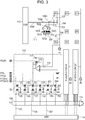
- Fig. 3 is an equivalent circuit diagram of an image pickup apparatus according to a second embodiment.
- a difference from the first embodiment is the configurations of the photoelectric conversion unit and the column circuit.
- the number of photoelectric conversion elements included in one photoelectric conversion unit is 3, and accordingly the number of storage capacitors included in the column circuit is 6.
- Components having the same functions as in the first embodiment are given the same reference numerals, and detailed description thereof is omitted.
- a photoelectric conversion unit 200 includes photoelectric conversion elements 101A to 101C. Since the number of photoelectric conversion elements included in one pixel for capturing an image is larger than that in the first embodiment, more accurate focus detection is possible.
- Transfer transistors 102A to 102C that transfer charges of the photoelectric conversion elements 101A to 101C are included.
- a driving pulse for the transfer transistor 102C a driving pulse PTXC is added.
- a column circuit 210 includes a storage capacitor 201 for storing signals of the photoelectric conversion element 101A to 101C added to one another.
- a storage capacitor 202 for storing a noise level is included.
- Switches 203 to 206 corresponding to these components are also included.
- both the driving pulses PTXA and PTXB are switched to the high level.
- the signals of the photoelectric conversion elements 101A and 101B are added at the input node 103.
- both the driving pulses PTXA and PTXB are switched to the high level here, only the driving pulse PTXB may be switched to the high level.
- all of the driving pulses PTXA, PTXB, and PTXC are switched to the high level. By this operation, the charges of the photoelectric conversion elements 101A to 101C are added at the input node 103.
- the storage periods of the photoelectric conversion elements 101A to 101C can be the same, namely as a period from the time t2 to the time t17.
- a signal of only the photoelectric conversion element 101A or added signals of the photoelectric conversion elements 101A and 101B may be read.
- Fig. 5 is an equivalent circuit diagram of an image pickup apparatus according to a third embodiment.
- a difference from the first and second embodiments is that the amplification unit 104 is shared by a plurality of photoelectric conversion elements included in different photoelectric conversion units.
- a first photoelectric conversion unit including photoelectric conversion elements 501A and 501B and a second photoelectric conversion unit including photoelectric conversion elements 502A and 502B are included.
- Light collected by a first micro-lens is incident on the plurality of photoelectric conversion elements 501A and 501B included in the first photoelectric conversion unit and light collected by a second micro-lens is incident on the plurality of photoelectric conversion elements 502A and 502B included in the second photoelectric conversion unit.
- Transfer transistors 503A, 503B, 504A, and 504B are provided for the photoelectric conversion elements 501A, 501B, 502A and 502B, respectively.
- lines for supplying driving pulses to the transfer transistors 503A, 503B, 504A, and 504B drive lines 505A, 505B, 506A, and 506B, respectively, are provided.
- the amplification unit 104, the reset transistor 105, and the selection transistor 106 can be shared by a plurality of pixels for capturing an image. In doing so, the number of transistors included in one pixel for capturing an image can be decreased. As a result, the area of the photoelectric conversion elements can be increased.
- signals can be read as signals in different rows by performing an operation that is basically the same as the reading described with reference to Fig. 2 . More specifically, after a signal of the photoelectric conversion element 501A is read in the first photoelectric conversion unit, signals of the photoelectric conversion elements 501A and 501B are added to each other at the input node 103. In doing so, both a signal for the focus detection and signals for capturing an image can be generated. Next, after a signal of the photoelectric conversion element 502A is read in the second photoelectric conversion unit, signals of the photoelectric conversion elements 502A and 502B are added to each other at the input node 103. In doing so, both a signal for the focus detection and signals for capturing an image can be generated.
- the amplification unit 104 is shared by the two photoelectric conversion units that are different from each other. Therefore, the signals of the photoelectric conversion elements 501A and 502A are added at the input node 103 and signals of the photoelectric conversion elements 501B and 502B may be added to each other at the input node 103.
- a specific example of a driving timing is illustrated in Fig. 6 . Characteristics of the present embodiment will be mainly described.
- a driving pulse PTXA is supplied to the transfer transistor 503A
- a driving pulse PTXB (505B) is supplied to the transfer transistor 503B.
- a driving pulse PTXA (506A) is supplied to the transfer transistor 504A
- a driving pulse PTXB (506B) is supplied to the transfer transistor 504B.
- the signals of the photoelectric conversion element 501A and 502A included in different photoelectric conversion units are added to each other at the input node 103. These signals can be used as the signals for the focus detection.
- the driving pulses PTXA (505A), PTXB (505B), PTXA (506A), and PTXB (506B) are switched from the low level to the high level.
- the driving pulses PTXA (505A), PTXB (505B), PTXA (506A), and PTXB (506B) are switched from the low level to the high level.
- the signals of all the photoelectric conversion elements 501A, 501B, 502A, and 502B included in different photoelectric conversion units are added to each other at the input node 103. These signals are used as the signals for capturing an image.
- the signals for the focus detection are obtained by adding signals of a plurality of photoelectric conversion elements included in different photoelectric conversion units with one another through this operation, the S/N ratio improves. Therefore, more accurate focus detection is possible.
- Fig. 7 is an equivalent circuit diagram of an image pickup apparatus according to a fourth embodiment.
- a difference of the present embodiment from the third embodiment is that a switch for electrically connecting a plurality of input nodes 103 to one another is provided.
- Components having functions similar to those of the configurations according to the first to third embodiments are given similar reference numerals, and detailed description thereof is omitted.
- a first photoelectric conversion unit includes photoelectric conversion elements 701A and 701B.
- a second photoelectric conversion unit includes photoelectric conversion elements 702A and 702B.
- a third photoelectric conversion unit includes photoelectric conversion elements 721A and 721B.
- a fourth photoelectric conversion unit includes photoelectric conversion elements 722A and 722B.
- An amplification unit 707 shared by the first and second photoelectric conversion units is provided.
- An amplification unit 727 shared by the third and fourth photoelectric conversion units is provided.
- Transfer transistors 703A, 703B, 704A, 704B, 723A, 723B, 724A, and 724B are provided for these photoelectric conversion elements, respectively.
- Drive lines 705A, 705B, 706A, 706B, 725A, 725B, 726A, and 726B for driving these transfer transistors, respectively, are provided.
- a switch 740 electrically connects input nodes of the amplification units 707 and 727 to each other.
- the switch 740 is controlled by a drive line 741.
- Fig. 8 is a driving pulse diagram of Fig. 7 .
- a driving pulse PTXA (705A) is a pulse supplied to the drive line 705A.
- a driving pulse PTXB (705B) is a pulse supplied to the drive line 705B.
- a driving pulse PTXA (725A) is a pulse supplied to the drive line 725A.
- a driving pulse PTXB (725B) is a pulse supplied to the drive line 725B.
- a driving pulse PVADD (741) is a pulse supplied to the drive line 741.
- Fig. 8 an example in which signals of the photoelectric conversion elements 701A and 721A included in the first photoelectric conversion unit and the third photoelectric conversion unit, respectively, are added to each other is illustrated.
- the driving pulse PVADD (741) is kept at the high level during a period illustrated in Fig. 8 . That is, the inputs nodes of the amplification units 707 and 727 are electrically connected to each other constantly.
- the signals of the photoelectric conversion elements 701A and 721A included in different photoelectric conversion units are transferred to the corresponding amplification units 707 and 727, respectively. Since the switch 740 is closed, the signals are added to each other. These signals can be used as the signals for the focus detection.
- the driving pulses PTXA (705A), PTXB (705B), PTXA (725A), and PTXB (725B) are switched from the low level to the high level.
- the driving pulses PTXA (705A), PTXB (705B), PTXA (725A), and PTXB (725B) are switched from the high level to the low level.
- signals of the plurality of photoelectric conversion elements 701A, 701B, 721A, and 721B included in different photoelectric conversion units are transferred to the corresponding amplification units 707 and 727. Since the switch 740 is closed, all the signals are added to one another. These signals can be used as the signals for capturing an image.
- the switch for electrically connecting the plurality of input nodes is added.
- This is desirable when signals of the same color are separated from one another in an image pickup apparatus including color filters, that is, for example, when the image pickup apparatus includes color filters arranged in a Bayer pattern. This is because it is possible to add the signals of photoelectric conversion elements of the same color that are arranged separately from one another to one another. Therefore, not only the focus detection but also the S/N ratio of image signals can be improved, thereby realizing accurate focus detection while obtaining high-quality image information.
- the present invention is not limited to the above embodiments and may be modified or altered in various ways.
- the circuit configurations of pixels are not limited to those described above, and a configuration in which selection and deselection are switched by switching the potential of an input node using a reset unit without including a selection unit may be adopted.
- a configuration in which an operational amplifier is included as a column circuit has been described, a simple configuration such as that of a common-source amplification circuit may be adopted, instead.
- various modifications are possible such as a configuration in which a plurality of gain stages are provided and a configuration in which an adding between a gain stage and a buffer stage is used.
- one common output line is provided for a pixel column in the above embodiments, a plurality of common output lines may be provided for one pixel column.
- a signal for focus detection is generated by a first operation, in which a signal of at least one photoelectric conversion element (101A) included in a photoelectric conversion unit (100) is read to an input node (103) of an amplification unit (104) and the signal is supplied to a common output line (107) by the amplification unit and signals for forming an image are generated by a second operation, in which a signal of another photoelectric conversion element (101B) included in the same photoelectric conversion unit as that including the at least one photoelectric conversion element from which the signal has been read in the first operation is read to the input node of the amplification unit while holding the signal read in the first operation using the amplification unit and the signals are supplied to the common output line by the amplification unit.
Landscapes
- Engineering & Computer Science (AREA)
- Multimedia (AREA)
- Signal Processing (AREA)
- Transforming Light Signals Into Electric Signals (AREA)
- Focusing (AREA)
- Studio Devices (AREA)
- Automatic Focus Adjustment (AREA)
Applications Claiming Priority (1)
| Application Number | Priority Date | Filing Date | Title |
|---|---|---|---|
| JP2011248823A JP5755111B2 (ja) | 2011-11-14 | 2011-11-14 | 撮像装置の駆動方法 |
Publications (3)
| Publication Number | Publication Date |
|---|---|
| EP2592826A2 EP2592826A2 (en) | 2013-05-15 |
| EP2592826A3 EP2592826A3 (en) | 2014-01-08 |
| EP2592826B1 true EP2592826B1 (en) | 2018-09-12 |
Family
ID=47428471
Family Applications (1)
| Application Number | Title | Priority Date | Filing Date |
|---|---|---|---|
| EP12191017.8A Active EP2592826B1 (en) | 2011-11-14 | 2012-11-02 | Method for driving image pickup apparatus |
Country Status (4)
| Country | Link |
|---|---|
| US (2) | US8773560B2 (enExample) |
| EP (1) | EP2592826B1 (enExample) |
| JP (1) | JP5755111B2 (enExample) |
| CN (2) | CN106060405B (enExample) |
Families Citing this family (45)
| Publication number | Priority date | Publication date | Assignee | Title |
|---|---|---|---|---|
| JP5893572B2 (ja) | 2012-03-01 | 2016-03-23 | キヤノン株式会社 | 撮像装置、撮像システム、撮像装置の駆動方法 |
| JP5813047B2 (ja) * | 2013-04-26 | 2015-11-17 | キヤノン株式会社 | 撮像装置、および、撮像システム。 |
| JP6112963B2 (ja) * | 2013-05-10 | 2017-04-12 | キヤノン株式会社 | 撮像装置 |
| JP2014222863A (ja) * | 2013-05-14 | 2014-11-27 | キヤノン株式会社 | 撮像装置 |
| JP6230329B2 (ja) * | 2013-08-19 | 2017-11-15 | キヤノン株式会社 | 撮像装置 |
| JP6177060B2 (ja) * | 2013-09-05 | 2017-08-09 | キヤノン株式会社 | 光電変換装置、撮像システム、および光電変換装置の駆動方法 |
| JP2015198315A (ja) * | 2014-04-01 | 2015-11-09 | キヤノン株式会社 | 固体撮像装置及び撮像システム |
| JP6338436B2 (ja) | 2014-04-25 | 2018-06-06 | キヤノン株式会社 | 撮像装置及びその制御方法 |
| JP6463000B2 (ja) * | 2014-05-02 | 2019-01-30 | キヤノン株式会社 | 固体撮像装置及び撮像システム |
| JP6391302B2 (ja) | 2014-05-23 | 2018-09-19 | キヤノン株式会社 | 撮像装置、および、撮像システム |
| JP6442261B2 (ja) * | 2014-06-05 | 2018-12-19 | キヤノン株式会社 | 撮像素子及び撮像装置、及びその制御方法 |
| JP6254048B2 (ja) | 2014-06-05 | 2017-12-27 | ルネサスエレクトロニクス株式会社 | 半導体装置 |
| JP6557455B2 (ja) * | 2014-06-25 | 2019-08-07 | キヤノン株式会社 | 撮像装置及びその制御方法、プログラム、記憶媒体 |
| JP6403461B2 (ja) * | 2014-07-01 | 2018-10-10 | キヤノン株式会社 | 撮像装置及びその駆動方法 |
| JP6494207B2 (ja) * | 2014-07-31 | 2019-04-03 | キヤノン株式会社 | 光電変換装置、光電変換システム、光電変換装置の駆動方法 |
| JP6682175B2 (ja) * | 2014-07-31 | 2020-04-15 | キヤノン株式会社 | 固体撮像素子および撮像システム |
| JP6362478B2 (ja) | 2014-08-27 | 2018-07-25 | ルネサスエレクトロニクス株式会社 | 半導体装置の製造方法および半導体装置 |
| JP6525539B2 (ja) * | 2014-10-08 | 2019-06-05 | キヤノン株式会社 | 撮像素子及び撮像装置 |
| JP2016082306A (ja) | 2014-10-10 | 2016-05-16 | キヤノン株式会社 | 撮像装置、撮像システム及び撮像装置の駆動方法 |
| JP6406977B2 (ja) * | 2014-11-04 | 2018-10-17 | キヤノン株式会社 | 光電変換装置、撮像システム |
| JP6478600B2 (ja) * | 2014-12-04 | 2019-03-06 | キヤノン株式会社 | 撮像装置およびその制御方法 |
| JP6580069B2 (ja) | 2014-12-26 | 2019-09-25 | キヤノン株式会社 | 撮像装置の駆動方法、撮像装置、撮像システム |
| JP6218799B2 (ja) | 2015-01-05 | 2017-10-25 | キヤノン株式会社 | 撮像素子及び撮像装置 |
| US10070088B2 (en) | 2015-01-05 | 2018-09-04 | Canon Kabushiki Kaisha | Image sensor and image capturing apparatus for simultaneously performing focus detection and image generation |
| JP2016131346A (ja) * | 2015-01-15 | 2016-07-21 | キヤノン株式会社 | 制御装置、撮像装置、制御方法、プログラム、記憶媒体 |
| JP6555890B2 (ja) | 2015-01-23 | 2019-08-07 | キヤノン株式会社 | 撮像装置、撮像システム、および撮像装置の駆動方法 |
| JP6478718B2 (ja) | 2015-03-05 | 2019-03-06 | キヤノン株式会社 | 撮像素子および撮像装置 |
| US10163948B2 (en) * | 2015-07-23 | 2018-12-25 | Semiconductor Energy Laboratory Co., Ltd. | Imaging device and electronic device |
| JP6595839B2 (ja) | 2015-08-05 | 2019-10-23 | キヤノン株式会社 | 撮像素子およびその制御方法、ならびに撮像装置 |
| JP6602109B2 (ja) | 2015-08-28 | 2019-11-06 | キヤノン株式会社 | 制御装置、撮像装置、制御方法、プログラム、および、記憶媒体 |
| JP6762710B2 (ja) | 2015-12-14 | 2020-09-30 | キヤノン株式会社 | 撮像装置及びその制御方法 |
| JP6739272B2 (ja) * | 2016-07-29 | 2020-08-12 | キヤノン株式会社 | 撮像装置、その制御方法、及びプログラム |
| US10270997B2 (en) * | 2016-09-08 | 2019-04-23 | Gvbb Holdings S.A.R.L. | Cross pixel interconnection |
| WO2019026287A1 (ja) | 2017-08-04 | 2019-02-07 | 株式会社ソニー・インタラクティブエンタテインメント | 撮像装置および情報処理方法 |
| JP2019080223A (ja) | 2017-10-26 | 2019-05-23 | 株式会社ソニー・インタラクティブエンタテインメント | カメラシステム |
| JP7105062B2 (ja) | 2017-12-21 | 2022-07-22 | 株式会社ソニー・インタラクティブエンタテインメント | 画像処理装置、コンテンツ処理装置、コンテンツ処理システム、および画像処理方法 |
| JP7091080B2 (ja) * | 2018-02-05 | 2022-06-27 | キヤノン株式会社 | 装置、システム、および移動体 |
| JP7250428B2 (ja) | 2018-03-22 | 2023-04-03 | キヤノン株式会社 | 撮像装置およびその制御方法 |
| US10630897B2 (en) * | 2018-06-01 | 2020-04-21 | Semiconductor Components Industries, Llc | Image sensors with charge overflow capabilities |
| JP6703053B2 (ja) * | 2018-08-06 | 2020-06-03 | キヤノン株式会社 | 光電変換装置、光電変換システム |
| JP7321685B2 (ja) | 2018-08-22 | 2023-08-07 | キヤノン株式会社 | 撮像装置 |
| JP7227777B2 (ja) | 2019-02-04 | 2023-02-22 | キヤノン株式会社 | 撮像装置 |
| JP7455588B2 (ja) | 2020-01-17 | 2024-03-26 | キヤノン株式会社 | 撮像装置 |
| JP2023059696A (ja) | 2021-10-15 | 2023-04-27 | キヤノン株式会社 | 撮像装置及びその制御方法 |
| JP2023088702A (ja) | 2021-12-15 | 2023-06-27 | キヤノン株式会社 | 撮像装置及びその制御方法 |
Family Cites Families (49)
| Publication number | Priority date | Publication date | Assignee | Title |
|---|---|---|---|---|
| KR19990084630A (ko) * | 1998-05-08 | 1999-12-06 | 김영환 | 씨모스 이미지 센서 및 그 구동 방법 |
| US6956605B1 (en) * | 1998-08-05 | 2005-10-18 | Canon Kabushiki Kaisha | Image pickup apparatus |
| US6657665B1 (en) * | 1998-12-31 | 2003-12-02 | Eastman Kodak Company | Active Pixel Sensor with wired floating diffusions and shared amplifier |
| US6819360B1 (en) * | 1999-04-01 | 2004-11-16 | Olympus Corporation | Image pickup element and apparatus for focusing |
| JP5002086B2 (ja) | 1999-10-28 | 2012-08-15 | キヤノン株式会社 | 焦点検出装置と撮像装置 |
| JP2002101341A (ja) * | 2000-09-26 | 2002-04-05 | Canon Inc | 撮像装置及び撮像システム |
| US6750437B2 (en) * | 2000-08-28 | 2004-06-15 | Canon Kabushiki Kaisha | Image pickup apparatus that suitably adjusts a focus |
| JP2002076317A (ja) * | 2000-08-28 | 2002-03-15 | Canon Inc | 固体撮像装置および撮像システム |
| US6759641B1 (en) * | 2000-09-27 | 2004-07-06 | Rockwell Scientific Licensing, Llc | Imager with adjustable resolution |
| JP2004134867A (ja) * | 2002-10-08 | 2004-04-30 | Canon Inc | 固体撮像装置、その駆動方法、及び撮像システム |
| US7489352B2 (en) * | 2002-11-15 | 2009-02-10 | Micron Technology, Inc. | Wide dynamic range pinned photodiode active pixel sensor (APS) |
| CN1574370A (zh) * | 2003-05-30 | 2005-02-02 | 松下电器产业株式会社 | 固体摄像器件 |
| US7081608B2 (en) * | 2003-10-15 | 2006-07-25 | Micron Technology, Inc. | Pixel with differential readout |
| US20050083421A1 (en) * | 2003-10-16 | 2005-04-21 | Vladimir Berezin | Dynamic range enlargement in CMOS image sensors |
| US7542085B2 (en) * | 2003-11-26 | 2009-06-02 | Aptina Imaging Corporation | Image sensor with a capacitive storage node linked to transfer gate |
| US7443437B2 (en) * | 2003-11-26 | 2008-10-28 | Micron Technology, Inc. | Image sensor with a gated storage node linked to transfer gate |
| US7332786B2 (en) * | 2003-11-26 | 2008-02-19 | Micron Technology, Inc. | Anti-blooming storage pixel |
| US20050128327A1 (en) * | 2003-12-10 | 2005-06-16 | Bencuya Selim S. | Device and method for image sensing |
| JP2005197379A (ja) * | 2004-01-06 | 2005-07-21 | Sony Corp | 固体撮像装置および信号処理回路 |
| KR100871688B1 (ko) * | 2004-02-27 | 2008-12-08 | 삼성전자주식회사 | 고체 촬상 장치 및 그 구동 방법 |
| JP4074599B2 (ja) * | 2004-03-26 | 2008-04-09 | シャープ株式会社 | 増幅型固体撮像装置 |
| KR100690912B1 (ko) * | 2005-08-12 | 2007-03-09 | 삼성전자주식회사 | 전하 전송 특성이 향상된 4 공유 픽셀형 이미지 센서 |
| US7244918B2 (en) * | 2005-08-30 | 2007-07-17 | Micron Technology, Inc. | Method and apparatus providing a two-way shared storage gate on a four-way shared pixel |
| JP4650249B2 (ja) * | 2005-12-13 | 2011-03-16 | 船井電機株式会社 | 撮像装置 |
| US7626626B2 (en) * | 2006-01-13 | 2009-12-01 | Micron Technology, Inc. | Method and apparatus providing pixel storage gate charge sensing for electronic stabilization in imagers |
| WO2007086352A1 (ja) * | 2006-01-25 | 2007-08-02 | Kyocera Corporation | 撮像素子及びカメラモジュール |
| US7711261B2 (en) * | 2006-04-11 | 2010-05-04 | Nikon Corporation | Imaging device, camera and image processing method |
| JP5076528B2 (ja) * | 2007-02-06 | 2012-11-21 | 株式会社ニコン | 光電変換部の連結/分離構造、固体撮像素子及び撮像装置 |
| JP4389959B2 (ja) * | 2007-04-23 | 2009-12-24 | ソニー株式会社 | 固体撮像装置、固体撮像装置の信号処理方法および撮像装置 |
| JP5451111B2 (ja) * | 2008-03-11 | 2014-03-26 | キヤノン株式会社 | 焦点検出装置およびそれを有する撮像装置 |
| US8569671B2 (en) * | 2008-04-07 | 2013-10-29 | Cmosis Nv | Pixel array capable of performing pipelined global shutter operation including a first and second buffer amplifier |
| JP5058090B2 (ja) * | 2008-07-18 | 2012-10-24 | 株式会社東芝 | 固体撮像装置 |
| JP4661912B2 (ja) * | 2008-07-18 | 2011-03-30 | ソニー株式会社 | 固体撮像素子およびカメラシステム |
| JP5422985B2 (ja) * | 2008-12-08 | 2014-02-19 | ソニー株式会社 | 画素回路、固体撮像素子、およびカメラシステム |
| FR2939999B1 (fr) * | 2008-12-12 | 2011-02-25 | E2V Semiconductors | Capteur d'image a double transfert de charges pour grande dynamique et procede de lecture |
| KR20100080172A (ko) * | 2008-12-31 | 2010-07-08 | 주식회사 동부하이텍 | 이미지 센서 및 그 제조 방법 |
| US8913166B2 (en) * | 2009-01-21 | 2014-12-16 | Canon Kabushiki Kaisha | Solid-state imaging apparatus |
| US8570427B2 (en) * | 2009-01-28 | 2013-10-29 | Nikon Corporation | Image-capturing device having focus adjustment function, image creation method including focus adjustment function, and program product for image-capturing device having focus adjustment function |
| JP5278165B2 (ja) * | 2009-05-26 | 2013-09-04 | ソニー株式会社 | 焦点検出装置、撮像素子および電子カメラ |
| JP5564909B2 (ja) * | 2009-11-30 | 2014-08-06 | ソニー株式会社 | 固体撮像装置とその製造方法、及び電子機器 |
| JP5091964B2 (ja) * | 2010-03-05 | 2012-12-05 | 株式会社東芝 | 固体撮像装置 |
| JP5511541B2 (ja) * | 2010-06-24 | 2014-06-04 | キヤノン株式会社 | 固体撮像装置及び固体撮像装置の駆動方法 |
| JP5729947B2 (ja) * | 2010-08-27 | 2015-06-03 | キヤノン株式会社 | 光電変換装置、焦点検出装置、および撮像システム |
| JP5664141B2 (ja) * | 2010-11-08 | 2015-02-04 | ソニー株式会社 | 固体撮像素子およびカメラシステム |
| FR2976121A1 (fr) * | 2011-05-31 | 2012-12-07 | St Microelectronics Sa | Dispositif d'imagerie matriciel comprenant au moins un ensemble de photosites a multiples temps d'integration. |
| JP5743837B2 (ja) * | 2011-10-07 | 2015-07-01 | キヤノン株式会社 | 光電変換装置、撮像装置および撮像システム |
| JP5959829B2 (ja) * | 2011-11-09 | 2016-08-02 | キヤノン株式会社 | 固体撮像装置 |
| JP5967915B2 (ja) * | 2011-12-09 | 2016-08-10 | キヤノン株式会社 | 固体撮像装置の駆動方法 |
| JP5968146B2 (ja) * | 2012-07-31 | 2016-08-10 | キヤノン株式会社 | 固体撮像装置およびカメラ |
-
2011
- 2011-11-14 JP JP2011248823A patent/JP5755111B2/ja active Active
-
2012
- 2012-11-02 EP EP12191017.8A patent/EP2592826B1/en active Active
- 2012-11-12 US US13/674,244 patent/US8773560B2/en active Active
- 2012-11-14 CN CN201610575546.9A patent/CN106060405B/zh active Active
- 2012-11-14 CN CN201210454913.1A patent/CN103108144B/zh not_active Expired - Fee Related
-
2014
- 2014-05-23 US US14/286,835 patent/US8928791B2/en active Active
Non-Patent Citations (1)
| Title |
|---|
| None * |
Also Published As
| Publication number | Publication date |
|---|---|
| CN106060405B (zh) | 2019-04-19 |
| EP2592826A2 (en) | 2013-05-15 |
| CN103108144B (zh) | 2016-08-10 |
| US20130120624A1 (en) | 2013-05-16 |
| US8773560B2 (en) | 2014-07-08 |
| JP5755111B2 (ja) | 2015-07-29 |
| US8928791B2 (en) | 2015-01-06 |
| CN106060405A (zh) | 2016-10-26 |
| US20140253771A1 (en) | 2014-09-11 |
| JP2013106194A (ja) | 2013-05-30 |
| EP2592826A3 (en) | 2014-01-08 |
| CN103108144A (zh) | 2013-05-15 |
Similar Documents
| Publication | Publication Date | Title |
|---|---|---|
| EP2592826B1 (en) | Method for driving image pickup apparatus | |
| JP6482186B2 (ja) | 撮像装置及びその駆動方法 | |
| US9232165B2 (en) | Solid-state imaging apparatus and method for driving solid-state imaging apparatus | |
| US20080211948A1 (en) | Photoelectric conversion apparatus and image sensing system using the same | |
| JP2016201649A (ja) | 撮像装置、撮像システム、および撮像装置の駆動方法 | |
| JP2014222863A (ja) | 撮像装置 | |
| US20180288346A1 (en) | Photoelectric conversion apparatus and photoelectric conversion system | |
| JP2012199913A (ja) | 信号受信部テスト回路、撮像装置、信号受信部テスト方法、撮像装置のテスト方法 | |
| US9800810B2 (en) | Imaging apparatus and imaging system | |
| JP2016082306A (ja) | 撮像装置、撮像システム及び撮像装置の駆動方法 | |
| US20170180665A1 (en) | Method for driving image capture device, image capture device, and image capture system | |
| RU2637728C2 (ru) | Способ возбуждения для устройства фиксации изображений и устройство фиксации изображений | |
| US20160006917A1 (en) | Imaging device and method of driving imaging device | |
| US9743030B2 (en) | Driving method for image pickup apparatus, and image pickup apparatus | |
| US20180176491A1 (en) | Image pickup device | |
| JP6214596B2 (ja) | 撮像装置の駆動方法 | |
| US9906750B2 (en) | Image pickup device driving method, image pickup device, and image pickup system using reset cancellation | |
| US9264640B2 (en) | Photoelectric conversion apparatus, method for driving photoelectric conversion apparatus, and imaging system | |
| US20240430596A1 (en) | Image capturing apparatus, control method thereof, and storage medium | |
| JP2007013362A (ja) | 撮像装置及び撮像方法 | |
| US11218661B2 (en) | Signal processing apparatus, photoelectric conversion apparatus, imaging apparatus, and moving body | |
| US9807333B2 (en) | Imaging apparatus and imaging system |
Legal Events
| Date | Code | Title | Description |
|---|---|---|---|
| PUAI | Public reference made under article 153(3) epc to a published international application that has entered the european phase |
Free format text: ORIGINAL CODE: 0009012 |
|
| AK | Designated contracting states |
Kind code of ref document: A2 Designated state(s): AL AT BE BG CH CY CZ DE DK EE ES FI FR GB GR HR HU IE IS IT LI LT LU LV MC MK MT NL NO PL PT RO RS SE SI SK SM TR |
|
| AX | Request for extension of the european patent |
Extension state: BA ME |
|
| PUAL | Search report despatched |
Free format text: ORIGINAL CODE: 0009013 |
|
| AK | Designated contracting states |
Kind code of ref document: A3 Designated state(s): AL AT BE BG CH CY CZ DE DK EE ES FI FR GB GR HR HU IE IS IT LI LT LU LV MC MK MT NL NO PL PT RO RS SE SI SK SM TR |
|
| AX | Request for extension of the european patent |
Extension state: BA ME |
|
| RIC1 | Information provided on ipc code assigned before grant |
Ipc: H04N 5/3745 20110101AFI20131202BHEP Ipc: H04N 5/335 20110101ALI20131202BHEP |
|
| 17P | Request for examination filed |
Effective date: 20140318 |
|
| RBV | Designated contracting states (corrected) |
Designated state(s): AL AT BE BG CH CY CZ DE DK EE ES FI FR GB GR HR HU IE IS IT LI LT LU LV MC MK MT NL NO PL PT RO RS SE SI SK SM TR |
|
| 17Q | First examination report despatched |
Effective date: 20160916 |
|
| REG | Reference to a national code |
Ref country code: DE Ref legal event code: R079 Ref document number: 602012050908 Country of ref document: DE Free format text: PREVIOUS MAIN CLASS: H04N0005374500 Ipc: H04N0005343000 |
|
| GRAP | Despatch of communication of intention to grant a patent |
Free format text: ORIGINAL CODE: EPIDOSNIGR1 |
|
| RIC1 | Information provided on ipc code assigned before grant |
Ipc: H04N 5/369 20110101ALI20180308BHEP Ipc: H04N 5/232 20060101ALI20180308BHEP Ipc: H04N 5/353 20110101ALI20180308BHEP Ipc: H04N 5/343 20110101AFI20180308BHEP Ipc: H01L 27/146 20060101ALI20180308BHEP Ipc: H04N 5/335 20110101ALI20180308BHEP Ipc: H04N 5/3745 20110101ALI20180308BHEP |
|
| INTG | Intention to grant announced |
Effective date: 20180329 |
|
| RIN1 | Information on inventor provided before grant (corrected) |
Inventor name: MINOWA, MASAAKI Inventor name: ARISHIMA, YU Inventor name: OKITA, AKIRA |
|
| GRAS | Grant fee paid |
Free format text: ORIGINAL CODE: EPIDOSNIGR3 |
|
| GRAA | (expected) grant |
Free format text: ORIGINAL CODE: 0009210 |
|
| AK | Designated contracting states |
Kind code of ref document: B1 Designated state(s): AL AT BE BG CH CY CZ DE DK EE ES FI FR GB GR HR HU IE IS IT LI LT LU LV MC MK MT NL NO PL PT RO RS SE SI SK SM TR |
|
| REG | Reference to a national code |
Ref country code: GB Ref legal event code: FG4D |
|
| REG | Reference to a national code |
Ref country code: CH Ref legal event code: EP |
|
| REG | Reference to a national code |
Ref country code: IE Ref legal event code: FG4D |
|
| REG | Reference to a national code |
Ref country code: DE Ref legal event code: R096 Ref document number: 602012050908 Country of ref document: DE |
|
| REG | Reference to a national code |
Ref country code: AT Ref legal event code: REF Ref document number: 1041972 Country of ref document: AT Kind code of ref document: T Effective date: 20181015 |
|
| REG | Reference to a national code |
Ref country code: NL Ref legal event code: MP Effective date: 20180912 |
|
| REG | Reference to a national code |
Ref country code: LT Ref legal event code: MG4D |
|
| PG25 | Lapsed in a contracting state [announced via postgrant information from national office to epo] |
Ref country code: BG Free format text: LAPSE BECAUSE OF FAILURE TO SUBMIT A TRANSLATION OF THE DESCRIPTION OR TO PAY THE FEE WITHIN THE PRESCRIBED TIME-LIMIT Effective date: 20181212 Ref country code: SE Free format text: LAPSE BECAUSE OF FAILURE TO SUBMIT A TRANSLATION OF THE DESCRIPTION OR TO PAY THE FEE WITHIN THE PRESCRIBED TIME-LIMIT Effective date: 20180912 Ref country code: LT Free format text: LAPSE BECAUSE OF FAILURE TO SUBMIT A TRANSLATION OF THE DESCRIPTION OR TO PAY THE FEE WITHIN THE PRESCRIBED TIME-LIMIT Effective date: 20180912 Ref country code: FI Free format text: LAPSE BECAUSE OF FAILURE TO SUBMIT A TRANSLATION OF THE DESCRIPTION OR TO PAY THE FEE WITHIN THE PRESCRIBED TIME-LIMIT Effective date: 20180912 Ref country code: RS Free format text: LAPSE BECAUSE OF FAILURE TO SUBMIT A TRANSLATION OF THE DESCRIPTION OR TO PAY THE FEE WITHIN THE PRESCRIBED TIME-LIMIT Effective date: 20180912 Ref country code: NO Free format text: LAPSE BECAUSE OF FAILURE TO SUBMIT A TRANSLATION OF THE DESCRIPTION OR TO PAY THE FEE WITHIN THE PRESCRIBED TIME-LIMIT Effective date: 20181212 Ref country code: GR Free format text: LAPSE BECAUSE OF FAILURE TO SUBMIT A TRANSLATION OF THE DESCRIPTION OR TO PAY THE FEE WITHIN THE PRESCRIBED TIME-LIMIT Effective date: 20181213 |
|
| PG25 | Lapsed in a contracting state [announced via postgrant information from national office to epo] |
Ref country code: AL Free format text: LAPSE BECAUSE OF FAILURE TO SUBMIT A TRANSLATION OF THE DESCRIPTION OR TO PAY THE FEE WITHIN THE PRESCRIBED TIME-LIMIT Effective date: 20180912 Ref country code: HR Free format text: LAPSE BECAUSE OF FAILURE TO SUBMIT A TRANSLATION OF THE DESCRIPTION OR TO PAY THE FEE WITHIN THE PRESCRIBED TIME-LIMIT Effective date: 20180912 Ref country code: LV Free format text: LAPSE BECAUSE OF FAILURE TO SUBMIT A TRANSLATION OF THE DESCRIPTION OR TO PAY THE FEE WITHIN THE PRESCRIBED TIME-LIMIT Effective date: 20180912 |
|
| REG | Reference to a national code |
Ref country code: AT Ref legal event code: MK05 Ref document number: 1041972 Country of ref document: AT Kind code of ref document: T Effective date: 20180912 |
|
| PG25 | Lapsed in a contracting state [announced via postgrant information from national office to epo] |
Ref country code: EE Free format text: LAPSE BECAUSE OF FAILURE TO SUBMIT A TRANSLATION OF THE DESCRIPTION OR TO PAY THE FEE WITHIN THE PRESCRIBED TIME-LIMIT Effective date: 20180912 Ref country code: NL Free format text: LAPSE BECAUSE OF FAILURE TO SUBMIT A TRANSLATION OF THE DESCRIPTION OR TO PAY THE FEE WITHIN THE PRESCRIBED TIME-LIMIT Effective date: 20180912 Ref country code: AT Free format text: LAPSE BECAUSE OF FAILURE TO SUBMIT A TRANSLATION OF THE DESCRIPTION OR TO PAY THE FEE WITHIN THE PRESCRIBED TIME-LIMIT Effective date: 20180912 Ref country code: IT Free format text: LAPSE BECAUSE OF FAILURE TO SUBMIT A TRANSLATION OF THE DESCRIPTION OR TO PAY THE FEE WITHIN THE PRESCRIBED TIME-LIMIT Effective date: 20180912 Ref country code: ES Free format text: LAPSE BECAUSE OF FAILURE TO SUBMIT A TRANSLATION OF THE DESCRIPTION OR TO PAY THE FEE WITHIN THE PRESCRIBED TIME-LIMIT Effective date: 20180912 Ref country code: CZ Free format text: LAPSE BECAUSE OF FAILURE TO SUBMIT A TRANSLATION OF THE DESCRIPTION OR TO PAY THE FEE WITHIN THE PRESCRIBED TIME-LIMIT Effective date: 20180912 Ref country code: RO Free format text: LAPSE BECAUSE OF FAILURE TO SUBMIT A TRANSLATION OF THE DESCRIPTION OR TO PAY THE FEE WITHIN THE PRESCRIBED TIME-LIMIT Effective date: 20180912 Ref country code: IS Free format text: LAPSE BECAUSE OF FAILURE TO SUBMIT A TRANSLATION OF THE DESCRIPTION OR TO PAY THE FEE WITHIN THE PRESCRIBED TIME-LIMIT Effective date: 20190112 Ref country code: PL Free format text: LAPSE BECAUSE OF FAILURE TO SUBMIT A TRANSLATION OF THE DESCRIPTION OR TO PAY THE FEE WITHIN THE PRESCRIBED TIME-LIMIT Effective date: 20180912 |
|
| PG25 | Lapsed in a contracting state [announced via postgrant information from national office to epo] |
Ref country code: SK Free format text: LAPSE BECAUSE OF FAILURE TO SUBMIT A TRANSLATION OF THE DESCRIPTION OR TO PAY THE FEE WITHIN THE PRESCRIBED TIME-LIMIT Effective date: 20180912 Ref country code: PT Free format text: LAPSE BECAUSE OF FAILURE TO SUBMIT A TRANSLATION OF THE DESCRIPTION OR TO PAY THE FEE WITHIN THE PRESCRIBED TIME-LIMIT Effective date: 20190112 Ref country code: SM Free format text: LAPSE BECAUSE OF FAILURE TO SUBMIT A TRANSLATION OF THE DESCRIPTION OR TO PAY THE FEE WITHIN THE PRESCRIBED TIME-LIMIT Effective date: 20180912 |
|
| REG | Reference to a national code |
Ref country code: DE Ref legal event code: R097 Ref document number: 602012050908 Country of ref document: DE |
|
| REG | Reference to a national code |
Ref country code: CH Ref legal event code: PL |
|
| PLBE | No opposition filed within time limit |
Free format text: ORIGINAL CODE: 0009261 |
|
| STAA | Information on the status of an ep patent application or granted ep patent |
Free format text: STATUS: NO OPPOSITION FILED WITHIN TIME LIMIT |
|
| PG25 | Lapsed in a contracting state [announced via postgrant information from national office to epo] |
Ref country code: MC Free format text: LAPSE BECAUSE OF FAILURE TO SUBMIT A TRANSLATION OF THE DESCRIPTION OR TO PAY THE FEE WITHIN THE PRESCRIBED TIME-LIMIT Effective date: 20180912 Ref country code: LU Free format text: LAPSE BECAUSE OF NON-PAYMENT OF DUE FEES Effective date: 20181102 Ref country code: DK Free format text: LAPSE BECAUSE OF FAILURE TO SUBMIT A TRANSLATION OF THE DESCRIPTION OR TO PAY THE FEE WITHIN THE PRESCRIBED TIME-LIMIT Effective date: 20180912 |
|
| REG | Reference to a national code |
Ref country code: BE Ref legal event code: MM Effective date: 20181130 |
|
| 26N | No opposition filed |
Effective date: 20190613 |
|
| REG | Reference to a national code |
Ref country code: IE Ref legal event code: MM4A |
|
| PG25 | Lapsed in a contracting state [announced via postgrant information from national office to epo] |
Ref country code: LI Free format text: LAPSE BECAUSE OF NON-PAYMENT OF DUE FEES Effective date: 20181130 Ref country code: CH Free format text: LAPSE BECAUSE OF NON-PAYMENT OF DUE FEES Effective date: 20181130 Ref country code: SI Free format text: LAPSE BECAUSE OF FAILURE TO SUBMIT A TRANSLATION OF THE DESCRIPTION OR TO PAY THE FEE WITHIN THE PRESCRIBED TIME-LIMIT Effective date: 20180912 |
|
| PG25 | Lapsed in a contracting state [announced via postgrant information from national office to epo] |
Ref country code: IE Free format text: LAPSE BECAUSE OF NON-PAYMENT OF DUE FEES Effective date: 20181102 Ref country code: FR Free format text: LAPSE BECAUSE OF NON-PAYMENT OF DUE FEES Effective date: 20181112 |
|
| PG25 | Lapsed in a contracting state [announced via postgrant information from national office to epo] |
Ref country code: BE Free format text: LAPSE BECAUSE OF NON-PAYMENT OF DUE FEES Effective date: 20181130 |
|
| PG25 | Lapsed in a contracting state [announced via postgrant information from national office to epo] |
Ref country code: MT Free format text: LAPSE BECAUSE OF NON-PAYMENT OF DUE FEES Effective date: 20181102 |
|
| PG25 | Lapsed in a contracting state [announced via postgrant information from national office to epo] |
Ref country code: TR Free format text: LAPSE BECAUSE OF FAILURE TO SUBMIT A TRANSLATION OF THE DESCRIPTION OR TO PAY THE FEE WITHIN THE PRESCRIBED TIME-LIMIT Effective date: 20180912 |
|
| PG25 | Lapsed in a contracting state [announced via postgrant information from national office to epo] |
Ref country code: CY Free format text: LAPSE BECAUSE OF FAILURE TO SUBMIT A TRANSLATION OF THE DESCRIPTION OR TO PAY THE FEE WITHIN THE PRESCRIBED TIME-LIMIT Effective date: 20180912 Ref country code: MK Free format text: LAPSE BECAUSE OF NON-PAYMENT OF DUE FEES Effective date: 20180912 Ref country code: HU Free format text: LAPSE BECAUSE OF FAILURE TO SUBMIT A TRANSLATION OF THE DESCRIPTION OR TO PAY THE FEE WITHIN THE PRESCRIBED TIME-LIMIT; INVALID AB INITIO Effective date: 20121102 |
|
| REG | Reference to a national code |
Ref country code: DE Ref legal event code: R079 Ref document number: 602012050908 Country of ref document: DE Free format text: PREVIOUS MAIN CLASS: H04N0005343000 Ipc: H04N0025420000 |
|
| PGFP | Annual fee paid to national office [announced via postgrant information from national office to epo] |
Ref country code: DE Payment date: 20241022 Year of fee payment: 13 |
|
| PGFP | Annual fee paid to national office [announced via postgrant information from national office to epo] |
Ref country code: GB Payment date: 20241023 Year of fee payment: 13 |