EP2237327A2 - Halbleiterbauelementepaket - Google Patents
Halbleiterbauelementepaket Download PDFInfo
- Publication number
- EP2237327A2 EP2237327A2 EP09770336A EP09770336A EP2237327A2 EP 2237327 A2 EP2237327 A2 EP 2237327A2 EP 09770336 A EP09770336 A EP 09770336A EP 09770336 A EP09770336 A EP 09770336A EP 2237327 A2 EP2237327 A2 EP 2237327A2
- Authority
- EP
- European Patent Office
- Prior art keywords
- semiconductor device
- paste
- electrode
- device package
- package according
- Prior art date
- Legal status (The legal status is an assumption and is not a legal conclusion. Google has not performed a legal analysis and makes no representation as to the accuracy of the status listed.)
- Ceased
Links
Images


Classifications
-
- H—ELECTRICITY
- H10—SEMICONDUCTOR DEVICES; ELECTRIC SOLID-STATE DEVICES NOT OTHERWISE PROVIDED FOR
- H10H—INORGANIC LIGHT-EMITTING SEMICONDUCTOR DEVICES HAVING POTENTIAL BARRIERS
- H10H20/00—Individual inorganic light-emitting semiconductor devices having potential barriers, e.g. light-emitting diodes [LED]
- H10H20/80—Constructional details
- H10H20/85—Packages
- H10H20/858—Means for heat extraction or cooling
- H10H20/8581—Means for heat extraction or cooling characterised by their material
-
- H—ELECTRICITY
- H10—SEMICONDUCTOR DEVICES; ELECTRIC SOLID-STATE DEVICES NOT OTHERWISE PROVIDED FOR
- H10H—INORGANIC LIGHT-EMITTING SEMICONDUCTOR DEVICES HAVING POTENTIAL BARRIERS
- H10H20/00—Individual inorganic light-emitting semiconductor devices having potential barriers, e.g. light-emitting diodes [LED]
- H10H20/80—Constructional details
- H10H20/85—Packages
- H10H20/855—Optical field-shaping means, e.g. lenses
- H10H20/856—Reflecting means
-
- H—ELECTRICITY
- H10—SEMICONDUCTOR DEVICES; ELECTRIC SOLID-STATE DEVICES NOT OTHERWISE PROVIDED FOR
- H10H—INORGANIC LIGHT-EMITTING SEMICONDUCTOR DEVICES HAVING POTENTIAL BARRIERS
- H10H20/00—Individual inorganic light-emitting semiconductor devices having potential barriers, e.g. light-emitting diodes [LED]
- H10H20/80—Constructional details
- H10H20/85—Packages
- H10H20/857—Interconnections, e.g. lead-frames, bond wires or solder balls
-
- H—ELECTRICITY
- H10—SEMICONDUCTOR DEVICES; ELECTRIC SOLID-STATE DEVICES NOT OTHERWISE PROVIDED FOR
- H10H—INORGANIC LIGHT-EMITTING SEMICONDUCTOR DEVICES HAVING POTENTIAL BARRIERS
- H10H20/00—Individual inorganic light-emitting semiconductor devices having potential barriers, e.g. light-emitting diodes [LED]
- H10H20/80—Constructional details
- H10H20/85—Packages
- H10H20/858—Means for heat extraction or cooling
- H10H20/8585—Means for heat extraction or cooling being an interconnection
-
- H—ELECTRICITY
- H10—SEMICONDUCTOR DEVICES; ELECTRIC SOLID-STATE DEVICES NOT OTHERWISE PROVIDED FOR
- H10W—GENERIC PACKAGES, INTERCONNECTIONS, CONNECTORS OR OTHER CONSTRUCTIONAL DETAILS OF DEVICES COVERED BY CLASS H10
- H10W72/00—Interconnections or connectors in packages
- H10W72/071—Connecting or disconnecting
- H10W72/073—Connecting or disconnecting of die-attach connectors
- H10W72/07351—Connecting or disconnecting of die-attach connectors characterised by changes in properties of the die-attach connectors during connecting
- H10W72/07352—Connecting or disconnecting of die-attach connectors characterised by changes in properties of the die-attach connectors during connecting changes in structures or sizes
-
- H—ELECTRICITY
- H10—SEMICONDUCTOR DEVICES; ELECTRIC SOLID-STATE DEVICES NOT OTHERWISE PROVIDED FOR
- H10W—GENERIC PACKAGES, INTERCONNECTIONS, CONNECTORS OR OTHER CONSTRUCTIONAL DETAILS OF DEVICES COVERED BY CLASS H10
- H10W72/00—Interconnections or connectors in packages
- H10W72/071—Connecting or disconnecting
- H10W72/075—Connecting or disconnecting of bond wires
- H10W72/07551—Connecting or disconnecting of bond wires characterised by changes in properties of the bond wires during the connecting
- H10W72/07554—Connecting or disconnecting of bond wires characterised by changes in properties of the bond wires during the connecting changes in dispositions
-
- H—ELECTRICITY
- H10—SEMICONDUCTOR DEVICES; ELECTRIC SOLID-STATE DEVICES NOT OTHERWISE PROVIDED FOR
- H10W—GENERIC PACKAGES, INTERCONNECTIONS, CONNECTORS OR OTHER CONSTRUCTIONAL DETAILS OF DEVICES COVERED BY CLASS H10
- H10W72/00—Interconnections or connectors in packages
- H10W72/30—Die-attach connectors
- H10W72/321—Structures or relative sizes of die-attach connectors
-
- H—ELECTRICITY
- H10—SEMICONDUCTOR DEVICES; ELECTRIC SOLID-STATE DEVICES NOT OTHERWISE PROVIDED FOR
- H10W—GENERIC PACKAGES, INTERCONNECTIONS, CONNECTORS OR OTHER CONSTRUCTIONAL DETAILS OF DEVICES COVERED BY CLASS H10
- H10W72/00—Interconnections or connectors in packages
- H10W72/50—Bond wires
- H10W72/541—Dispositions of bond wires
- H10W72/547—Dispositions of multiple bond wires
-
- H—ELECTRICITY
- H10—SEMICONDUCTOR DEVICES; ELECTRIC SOLID-STATE DEVICES NOT OTHERWISE PROVIDED FOR
- H10W—GENERIC PACKAGES, INTERCONNECTIONS, CONNECTORS OR OTHER CONSTRUCTIONAL DETAILS OF DEVICES COVERED BY CLASS H10
- H10W72/00—Interconnections or connectors in packages
- H10W72/851—Dispositions of multiple connectors or interconnections
- H10W72/874—On different surfaces
- H10W72/884—Die-attach connectors and bond wires
-
- H—ELECTRICITY
- H10—SEMICONDUCTOR DEVICES; ELECTRIC SOLID-STATE DEVICES NOT OTHERWISE PROVIDED FOR
- H10W—GENERIC PACKAGES, INTERCONNECTIONS, CONNECTORS OR OTHER CONSTRUCTIONAL DETAILS OF DEVICES COVERED BY CLASS H10
- H10W90/00—Package configurations
- H10W90/701—Package configurations characterised by the relative positions of pads or connectors relative to package parts
- H10W90/731—Package configurations characterised by the relative positions of pads or connectors relative to package parts of die-attach connectors
- H10W90/736—Package configurations characterised by the relative positions of pads or connectors relative to package parts of die-attach connectors between a chip and a stacked lead frame, conducting package substrate or heat sink
-
- H—ELECTRICITY
- H10—SEMICONDUCTOR DEVICES; ELECTRIC SOLID-STATE DEVICES NOT OTHERWISE PROVIDED FOR
- H10W—GENERIC PACKAGES, INTERCONNECTIONS, CONNECTORS OR OTHER CONSTRUCTIONAL DETAILS OF DEVICES COVERED BY CLASS H10
- H10W90/00—Package configurations
- H10W90/701—Package configurations characterised by the relative positions of pads or connectors relative to package parts
- H10W90/751—Package configurations characterised by the relative positions of pads or connectors relative to package parts of bond wires
- H10W90/756—Package configurations characterised by the relative positions of pads or connectors relative to package parts of bond wires between a chip and a stacked lead frame, conducting package substrate or heat sink
Definitions
- the present disclosure relates to a semiconductor device package.
- LEDs Light emitting diodes may form light emitting sources using GaAs-based, AlGaAs-based, GaN-based, InGaN-based, and InGaAIP-based compound semiconductor materials.
- LEDs are packaged to be used as light emitting devices that emit a variety of colors.
- Light emitting diodes are used as light sources in diverse applications, comprising on/off indicators, text displays, and image displays, that depict colors.
- Embodiments provide a semiconductor device package comprising a paste member that comprises reflective metal and is disposed between a semiconductor device and an electrode.
- Embodiments provide a semiconductor device package comprising a semiconductor device that is die-bonded on a paste member containing reflective metal or/and inorganic fillers.
- Embodiments provide a semiconductor device comprising a paste member that contains reflective metal or/and inorganic fillers and disposed in a paste groove of an electrode and an LED that is die-bonded on the paste member.
- An embodiment provides a semiconductor device package comprising: a package body; a plurality of electrodes comprising a first electrode on the package body; a paste member on the first electrode and comprising at least one of inorganic fillers and metal powder; and a semiconductor device die-bonded on the paste member.
- An embodiment provides a semiconductor device package comprising: a package body comprising a cavity; a plurality of electrodes comprising a first electrode in the cavity; a paste member on the first electrode and comprising a white inorganic fillers and a reflective metal; at least one light emitting diode chip die-bonded on the paste member; a wire electrically connecting the electrodes to the light emitting diode chip; and a resin material in the cavity.
- An embodiment provides a semiconductor device package comprising: a light emitting diode chip; a first electrode under the light emitting diode chip; a second electrode spaced apart from the first electrode; an organic paste member on the first electrode and comprising at least one of an inorganic fillers and a reflective metal, the light emitting diode chip being die-bonded on the organic paste member; and a connecting member connecting the light emitting diode chip to the electrodes.
- heat dissipation of a semiconductor device such as an LED chip can be improved by a paste member containing reflective metal.
- a yellowing problem of resin material can be solved by reducing a contact area between the paste member and the resin material.
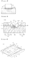
- Fig. 1 is a cross-sectional view of a semiconductor device package according to a first embodiment
- Fig. 2 is a top plan view of a first electrode on which a semiconductor device of Fig. 1 is mounted
- Fig. 3 is a cross-sectional view illustrating a heat dissipation path of a paste member of Fig. 1 .
- a semiconductor device package 100 comprises a package body 110, a semiconductor device 120, a resin material 125, a plurality of electrodes 132 and 134, and a paste member 140.
- the package body 110 may be formed of a material selected from the group consisting of polyphthalamide (PPA), liquid crystal polymer, resin-based material (e.g., syndiotactic polystyrene (SPS), a metal core printed circuit board (MCPCB), a printed circuit board (PCB), a ceramic PCB, a frame retardant-4 (FR-4), a aluminum nitride (AIN).
- PPA polyphthalamide
- MCPCB metal core printed circuit board
- PCB printed circuit board
- FR-4 frame retardant-4
- AIN aluminum nitride
- the package body 110 may be provided in the form of a chip-on-board (COB).
- a cavity 115 having an opened top is formed at an upper portion 112 of the package body 110 and an inner wall of the cavity 115 may be formed to be vertical or inclined at a predetermined angle with respective to a bottom surface thereof.
- the cavity 115 may be formed in a circular or polygonal shape and in a single layer cavity structure or a multi-layer cavity structure. However, the present disclosure is not limited to these configurations.
- the electrodes 132 and 134 are formed in the cavity 115 of the package body 110. First ends of the electrodes 132 and 134 are disposed in the cavity 115 and second ends of the electrodes 132 and 134 are exposed to an external side of the package body 110. The second ends of the electrodes 132 and 134 may be used as external electrodes P1 and P2. The second ends of the electrodes 132 and 134 extend to a side or bottom surface of the package body 110. However, the present disclosure is not limited to this configuration.
- the electrodes 132 and 134 may be formed by selectively using a lead frame type, a PCB (printed circuit board) type, a ceramic type, a plating type, and a via-hole type.
- the electrode 132 is provided at a first region with a paste groove 136 having a predetermined depth.
- the paste groove 136 may be formed through a punching process or an etching process.
- the paste groove 136 may be formed on the electrode 132 before or after the package body 110 is manufactured.
- the paste groove 136 may be formed on the electrode 132 on which the semiconductor device 120 is attached. The following will be described with an example where the paste groove 136 is formed on the first electrode 132.
- the paste groove 136 may be formed on a region where the semiconductor device 120 is die-bonded.
- the paste groove 136 may be formed in a circular shape, a polygonal shape, or a random shape.
- a depth of the paste groove 136 is 1-100 ⁇ m from a top surface of the electrode 132.
- the paste member 140 is formed in the paste groove 136.
- the paste member 140 may be formed through at least one of dotting, stamping, and dispensing processes.
- the paste member 140 may be formed of an organic paste material containing a reflective metal.
- the paste member 140 may be formed by mixing an organic resin with an inorganic fillers or/and a reflective metal at a predetermined ratio.
- the organic resin contains silicon or epoxy resin.
- the inorganic fillers contain high reflective white inorganic fillers or reflective inorganic fillers such as TiO 2 .
- the reflective metal may contain metal powder such as Ag and Al that are excellent in a reflective property and thermal conduction.
- the paste member 140 may be formed of the organic resin mixed with 0.1-30 wt% of the inorganic fillers or/and 0.1-30 wt% of the metal powder.
- the paste member 140 has a higher thermal conduction and reflective property than the resin material such as epoxy and has an equal insulation property as the epoxy.
- the bottom and outer circumference of the paste member 140 may surface-contact the first electrode 132.
- the semiconductor device 120 is die-bonded on the paste member 140.
- the semiconductor device 120 comprises, for example, an LED chip.
- the LED chip may be a colored LED chip such as a red LED chip, a green LED chip, or a blue LED chip or an ultraviolet LED chip.
- the package with the LED chip may be referred to as an LED package.
- the semiconductor device 120 may comprise a protective device such as a Zener diode.
- the paste member 140 may be designed such that at least one semiconductor device 120 may be die-bonded.
- the number of the semiconductor device 120 may be varied in accordance with the size of the paste groove 136.
- the paste member 140 has a first width D1 greater than a first width D2 of the semiconductor device 120. That is, an area of the paste member 140 may be greater than a bottom area of the semiconductor device 120.
- the semiconductor device 120 is connected to the electrodes 132 and 134 by wires 122 and 124.
- the resin material 125 is formed in the cavity 115.
- the resin material 125 comprises transparent silicon or epoxy resin. Phosphors may be added to the resin material 125.
- a lens (not shown) formed in a predetermined shape may be attached or formed on the resin material 125.
- the package boy 110 may comprise a protective device (not shown) such as a Zener diode for protecting the semiconductor device 120.
- electric power is supplied to the semiconductor device package 100 through the electrodes 132 and 134.
- the electrode 132 supplies a first polarity power to the semiconductor device 120 and the second electrode 134 supplies second polarity power to the semiconductor device 120.
- the semiconductor device 120 is the LED chip, the semiconductor device 120 emits light in all directions. In this case, the semiconductor device 120 generates heat. Some of the heat generated is conducted to the paste member 140 disposed under the semiconductor device 120 and the heat conducted to the paste member 140 is dissipated through the first electrode 132.
- the paste member 140 surface-contacts the paste groove 136 of the first electrode 132 to dissipate the heat conducted from the semiconductor device 120 through the first electrode 132.
- the paste member 140 is formed in the paste groove 136 of the first electrode 132 and disposed under the semiconductor device 120. Therefore, the contact area of the paste member 140 with the resin material 125 is reduced. Here, the paste member 140 may protrude above the first electrode 132.
- the paste member 140 since the paste member 140 has the higher thermal conduction efficiency, it can reduce a boundary surface temperature with the semiconductor device 120. Accordingly, the yellowing problem of the resin material 125 by the heat can be prevented.
- the paste member 140 contains the reflective metal, it can reflect some of the light emitted from the semiconductor device 120 or vary a critical angle of the light. Accordingly, an amount of the light reflected on the light emitting diode package can be improved.
- Fig. 4 is a cross-sectional view illustrating a semiconductor device package according to a second embodiment. Parts that are already described in the first embodiment will not be described in this second embodiment.
- a semiconductor device package of this second embodiment comprises a first electrode 132 on which paste grooves 136A formed in a protrusion/groove structures are formed.
- a paste member 140 is formed in the paste groove 136A.
- a contact area of the paste member 140 with the first electrode 132 can be increased by the protrusion/groove structures. Therefore, the heat generated by the semiconductor device 120 can be effectively dissipated and vary a critical angle of the light emitted from the LED chip or reflect or refract the light.
- Fig. 5 is a cross-sectional view illustrating a semiconductor device package according to a third embodiment. Parts that are already described in the first embodiment will not be described in this second embodiment.
- a semiconductor device package 100A comprises a multi-layered cavity 115A and a paste member 140A formed on a top surface of a first electrode 133.
- First and second electrodes 133 and 135 are disposed on the cavity 115A.
- a first end 133A of the first electrode 133 is disposed on a lower-layer bottom surface of the cavity 115A and a semiconductor device 120 is die-bonded on the first end 133A of the first electrode 133.
- the semiconductor device 120 is die-bonded by the paste member 140A formed on the top surface of the first electrode 133.
- the paste member 140A is formed on the top surface of the first end 133A of the first electrode 133. In this case, the heat dissipation efficiency can be improved in accordance with an area of the paste member 140A.
- the description of the paste member 140A will refer to the first embodiment.
- a first end 135B of the second electrode 135 and a middle end 133B of the first electrode 133 are obliquely disposed at a lower layer of the cavity 115A to improve the light reflection.
- a second end 133C of the first electrode 133 and a second end 135C of the second electrode 135 are exposed through middle and top ends of the cavity 115A.
- a transparent resin material 125 is formed in the cavity 115A. Phosphors may be added to the resin material 125.
- the resin material 125 may be provided at a lower cavity structure with a phosphor layer.
- a transparent resin layer may be formed in the cavity structure.
- the present disclosure is not limited to this.
- a plurality of wires 122 and 124 have first ends connected to the semiconductor device 120 and second ends connected to a second end 133C of the first electrode 133 and a second end 135C of the second electrode 135. Accordingly, a heat dissipation path of the semiconductor device 120 may be dispersed.
- the paste member 140A comprises a reflective metal and inorganic fillers and thus the heat generated by the semiconductor device 120 can be dissipated through the first electrode 132.
- Fig. 6 is a cross-sectional view illustrating a semiconductor device package according to a fourth embodiment and Fig. 7 is a side sectional view of Fig. 6 . Parts that are already described in the first embodiment will not be described in this second embodiment.
- a semiconductor device package 200 comprises a package body 210, a cavity 215, a plurality of electrodes 232 and 234, a paste member 240, a semiconductor device 220, and a resin material 225.
- the package body 210 is a silicon-based wafer level package (WLP) formed in a polyhedron shape.
- WLP wafer level package
- a cavity 215 having a predetermined depth may be formed in an upper portion of the package body 210.
- a circumference of the package body 210 may be inclined.
- the present disclosure is not limited to this.
- the electrodes 232 and 234 may be formed on a surface of the package body 210.
- the electrodes 232 and 234 may be formed on a top surface (comprising a cavity region), side surface, and rear surface of the package body 210.
- the electrodes 232 and 234 may be formed in a plating type or/and a via-hole type.
- a reflective material may be coated on a top surface of the electrodes 232 and 234.
- an insulating layer (not shown) may be formed between the package body 210 and the electrodes 232 and 234.
- the present disclosure is not limited to this.
- First ends of the electrodes 232 and 234 are disposed in the cavity 215 and spaced apart from each other.
- the electrode 232 is provided with a paste groove 236.
- the paste groove 236 may be formed with a predetermined depth by dry-etching or wet-etching of the electrode 232.
- the paste groove 236 may be formed in a circular shape, a polygonal shape, or a random shape.
- a size of the paste groove 236 may be equal to or greater than a bottom surface of the semiconductor device 220.
- the semiconductor device 220 may be at least one LED chip.
- the depth of the paste groove 236 may be 1-100 ⁇ m from the top surface of the electrode 232.
- a paste member 240 is formed in the paste groove 236.
- the paste member 240 may be formed through one of a dotting process, a stamping process, and a dispensing process.
- the paste member 240 may be formed of an organic paste material to which metal powder is added.
- the paste member 240 may be formed of organic resin to which inorganic fillers or/and metal powder is added at a predetermined ratio.
- the organic resin contains silicon or epoxy resin.
- the inorganic filler contains high reflective white inorganic fillers such as TiO 2 .
- the reflective metal may contain metal powder such as Ag and Al that are excellent in a reflective property and thermal conduction.
- the paste member 140 may be formed of the organic resin mixed with 0.1-30 wit% of the inorganic fillers or/and 0.1-30 wit% of the metal powder.
- the paste member 240 is applied on the paste groove 236 and the semiconductor device 220 is die-bonded on the paste member 240.
- the semiconductor device 220 is connected to the electrodes 232 and 234 by a wire 222.
- Heat generated by the semiconductor device 220 is conducted to the electrode 232 by the paste member 240. Therefore, a junction temperature between the semiconductor device 220 and the paste member 240 can be reduced.
- the shape, size, and number of the paste member 240 in the cavity 215 may be varied in accordance with the shape, size, and number of the semiconductor device 220.
- the paste member 240 may be formed in a large size or a plurality of the paste members 240 may be provided.
- the resin material 225 is formed in the cavity 215.
- the resin material 225 comprises transparent silicon or epoxy. Phosphors may be added to the resin material 225.
- a lens (not shown) for refracting light in a predetermined direction may be disposed on the resin material 225.
- a protective device such as a Zener diode for protecting the semiconductor device (i.e., LED) 220 may be provided on the package body 210.
- the semiconductor device 220 When electric power is applied from the electrodes 232 and 234, the semiconductor device 220 is driven to generate heat. The heat generated by the semiconductor device 220 is conducted to the electrode 232 through the paste member 240 and then dissipated. Further, when the semiconductor device 220 is an LED chip, the light emitted from the LED chip is partly reflected or refracted by the paste member 240.
- the heat generated by the semiconductor device 220 is conducted to the electrode 232 through the paste member 240 and then dissipated. Therefore, the yellowing problem of the resin material 225 contacting the semiconductor device 220 can be solved. Further, a contact area of the paste member 240 with the resin material 225 is reduced and a contact area of the paste member 240 with the electrode 132 is increased. Therefore, the heat dissipation efficiency of the paste member 240 can be enhanced.
- Fig. 8 is a cross-sectional view illustrating a semiconductor device package according to a fifth embodiment. Parts that are already described in the first embodiment will not be described in this second embodiment.
- a semiconductor package 300 comprises a package body 310, a semiconductor device 320, a plurality of electrodes 332 and 334, wires 322 and 324, a resin material 325, and a paste member 340.
- the electrodes 332 and 334 are formed on the package body 310.
- the electrodes 332 and 334 may be formed by selectively using a lead frame type, a PCB type, a ceramic type, a plating type, and a via-hole type.
- the electrode 332 may extend to one side of the top surface of the package body 310, a left side surface of the package body 310, and a rear surface of the package body 310.
- the second electrode 334 may extend to the other side of the top surface of the package body 310, a right side surface and rear surface of the package body 310.
- a rear electrode of the package body 310 may be used as external electrodes P5 and P6.
- a paste groove 336 is formed on a top surface of the first electrode 332 and the paste member 340 is formed in the paste groove 336.
- the paste member 340 may be mixed with metal powder or/and a white inorganic fillers.
- the paste member 340 corresponds to the paste member 340 of the first embodiment.
- At least one semiconductor device 320 is die-bonded on the paste member 340.
- the semiconductor device 320 may be an LED chip and electrically connected to the electrodes 332 and 334 by the wires 322 and 324.
- the resin material 325 may be formed in a lens shape using silicon or epoxy resin.
- the resin material 325 seals the semiconductor device 320 and the wires 322 and 324.
- the resin material 325 can refract the light emitted from the LED chip in a predetermined direction.
- a portion of the heat generated by the semiconductor device 320 is conducted to the electrode 332 through the paste member 340 and is then dissipated.
- a via-hole (not shown) may be formed through the electrode 332 and extend to a bottom surface of the package body 310. The via-hole functions to dissipate the heat through a lower portion of the package body 310.
- Fig. 9 is a cross-sectional view illustrating a semiconductor device package according to a sixth embodiment. Parts that are already described in the first embodiment will not be described in this second embodiment.
- a semiconductor package 300A comprises a package body 310, a paste member 340A, a semiconductor device 320A, a plurality of electrodes 332 and 334, a paste groove 336A, and a resin material 325.
- the paste groove 336A is formed in the electrode 332 of the package body 310.
- the paste groove 336A may be formed in a plurality of stripe shapes, ring shapes, or donut shapes.
- the paste member 340A is formed in the paste groove 336A. A portion of the electrode 332 is exposed in the past groove 336A and a conductive adhesive may be applied on a portion of the electrode 332.
- the semiconductor device 320A may be die-boned on the paste member 340A by the conductive adhesive. That is, both organic paste member and conductive paste member may be used as the die paste member.
- a bottom electrode of the LED chip is electrically connected to the electrode 332 and also connected to the electrode 334 by a wire 324.
- the bottom electrode of the LED chip may be an N-type or P-type electrode.
- the heat generated by the semiconductor device can be effectively dissipated by the thermal conductive paste member.
- the light emitted from the LED chip can be reflected by the paste member containing the metal powder.
- the semiconductor device package using the LED chip may be used as a light source of a front light or/and backlight of a liquid crystal display device and as lightings.
- a layer (or film) is referred to as being 'on' another layer or substrate, it can be directly on the another layer or substrate, or intervening layers may also be present. Further, it will be understood that when a layer is referred to as being 'under' another layer, it can be directly under the another layer, and one or more intervening layers may also be present. In addition, it will also be understood that when a layer is referred to as being 'between' two layers, it can be the only layer between the two layers, or one or more intervening layers may also be present.
- the embodiments provide a semiconductor device package.
- the embodiments provide an LED package.
- the embodiments also provide an LED package that can be used as a light source for a variety of fields such as lighting displays, letter displays and image displays.
Landscapes
- Led Device Packages (AREA)
- Solid State Image Pick-Up Elements (AREA)
- Wire Bonding (AREA)
- Die Bonding (AREA)
Applications Claiming Priority (2)
| Application Number | Priority Date | Filing Date | Title |
|---|---|---|---|
| KR1020080059069A KR101438826B1 (ko) | 2008-06-23 | 2008-06-23 | 발광장치 |
| PCT/KR2009/003212 WO2009157664A2 (ko) | 2008-06-23 | 2009-06-16 | 반도체 소자 패키지 |
Publications (2)
| Publication Number | Publication Date |
|---|---|
| EP2237327A2 true EP2237327A2 (de) | 2010-10-06 |
| EP2237327A4 EP2237327A4 (de) | 2011-10-26 |
Family
ID=41430292
Family Applications (1)
| Application Number | Title | Priority Date | Filing Date |
|---|---|---|---|
| EP09770336A Ceased EP2237327A4 (de) | 2008-06-23 | 2009-06-16 | Halbleiterbauelementepaket |
Country Status (5)
| Country | Link |
|---|---|
| US (2) | US8203218B2 (de) |
| EP (1) | EP2237327A4 (de) |
| KR (1) | KR101438826B1 (de) |
| CN (1) | CN101926014B (de) |
| WO (1) | WO2009157664A2 (de) |
Families Citing this family (31)
| Publication number | Priority date | Publication date | Assignee | Title |
|---|---|---|---|---|
| CN101749625B (zh) * | 2010-01-22 | 2014-07-16 | 深圳市中庆微科技开发有限公司 | 一种照明模块 |
| KR100993093B1 (ko) * | 2010-02-04 | 2010-11-08 | 엘지이노텍 주식회사 | 발광 소자 및 발광 소자 패키지 |
| KR100986397B1 (ko) * | 2010-02-08 | 2010-10-08 | 엘지이노텍 주식회사 | 발광 장치 |
| KR100999736B1 (ko) * | 2010-02-17 | 2010-12-08 | 엘지이노텍 주식회사 | 발광 소자, 발광 소자 제조방법 및 라이트 유닛 |
| KR101643410B1 (ko) * | 2010-03-08 | 2016-07-28 | 엘지이노텍 주식회사 | 발광 소자, 발광 소자 제조방법 및 발광 소자 패키지 |
| EP2365552A3 (de) * | 2010-03-09 | 2015-03-25 | LG Innotek Co., Ltd. | Lichtemittierendes Bauteil mit einem Anschlußträger der eine Einbuchtung aufweist. |
| KR101039937B1 (ko) * | 2010-04-28 | 2011-06-09 | 엘지이노텍 주식회사 | 발광소자, 발광소자의 제조방법, 발광소자 패키지 및 조명시스템 |
| KR101125335B1 (ko) | 2010-04-15 | 2012-03-27 | 엘지이노텍 주식회사 | 발광소자, 발광소자 제조방법 및 발광소자 패키지 |
| JP5528900B2 (ja) * | 2010-04-30 | 2014-06-25 | ローム株式会社 | 発光素子モジュール |
| KR101676669B1 (ko) * | 2010-05-20 | 2016-11-16 | 엘지이노텍 주식회사 | 발광 소자 |
| CN102652357B (zh) * | 2010-05-21 | 2015-09-09 | 丰田自动车株式会社 | 半导体装置 |
| CN102456812B (zh) * | 2010-10-28 | 2015-08-12 | 展晶科技(深圳)有限公司 | 发光二极管封装结构 |
| US20120112237A1 (en) * | 2010-11-05 | 2012-05-10 | Shenzhen China Star Optoelectronics Technology Co. Ltd. | Led package structure |
| CN102916089B (zh) * | 2011-08-01 | 2015-03-25 | 赛恩倍吉科技顾问(深圳)有限公司 | 发光二极管封装结构的形成方法及其基座的形成方法 |
| CN103152974B (zh) * | 2013-02-21 | 2016-03-16 | 金兴精密工业股份有限公司 | 一种使用金属线路片的电子线路板及其电子封装模块 |
| KR101958418B1 (ko) * | 2013-02-22 | 2019-03-14 | 삼성전자 주식회사 | 발광 소자 패키지 |
| CN104064663B (zh) * | 2013-03-21 | 2017-06-20 | 展晶科技(深圳)有限公司 | 发光二极管封装结构 |
| CN104112806A (zh) * | 2013-04-17 | 2014-10-22 | 展晶科技(深圳)有限公司 | 发光二极管及其封装结构 |
| JP6171613B2 (ja) * | 2013-06-21 | 2017-08-02 | 日亜化学工業株式会社 | 発光装置の製造方法及び発光装置 |
| US9954144B2 (en) | 2014-01-10 | 2018-04-24 | Cree, Inc. | Wafer level contact pad solder bumping for surface mount devices with non-planar recessed contacting surfaces |
| US20150200336A1 (en) * | 2014-01-10 | 2015-07-16 | Cree, Inc. | Wafer level contact pad standoffs with integrated reflector |
| JP6139427B2 (ja) * | 2014-02-04 | 2017-05-31 | Hoya Candeo Optronics株式会社 | 発光装置及びその製造方法 |
| TW201545828A (zh) * | 2014-06-10 | 2015-12-16 | Ya-Yang Yan | 一種放電加工切割線及該放電加工切割線之製造方法 |
| KR102346643B1 (ko) * | 2015-06-30 | 2022-01-03 | 쑤저우 레킨 세미컨덕터 컴퍼니 리미티드 | 발광 소자, 발광 소자 제조방법 및 발광 모듈 |
| JP6665731B2 (ja) * | 2016-08-22 | 2020-03-13 | 豊田合成株式会社 | 発光装置及びその製造方法 |
| DE102017115656A1 (de) * | 2017-07-12 | 2019-01-17 | Osram Opto Semiconductors Gmbh | Verfahren zur Herstellung eines optoelektronischen Bauelements und optoelektronisches Bauelement |
| JP7064325B2 (ja) * | 2017-12-18 | 2022-05-10 | スタンレー電気株式会社 | 半導体発光装置、および、それを用いた半導体発光装置の製造方法 |
| CN109628001A (zh) * | 2018-11-09 | 2019-04-16 | 李梅 | 一种用于FPC行业的sPS胶膜及其制备方法 |
| KR102912536B1 (ko) * | 2020-09-07 | 2026-01-14 | 삼성디스플레이 주식회사 | 표시 장치 및 이의 제조 방법 |
| CN115101500B (zh) * | 2022-06-08 | 2025-08-01 | 安徽积芯微电子科技有限公司 | 一种半导体芯片封装组件及其封装方法 |
| CN115782247B (zh) * | 2022-11-28 | 2024-06-11 | 华中科技大学 | 连续纤维增强复合材料的多自由度增材混编设备及方法 |
Family Cites Families (70)
| Publication number | Priority date | Publication date | Assignee | Title |
|---|---|---|---|---|
| US153835A (en) * | 1874-08-04 | Improvement in grain-separators | ||
| US221940A (en) * | 1879-11-25 | Improvement in hydraulic elevators | ||
| US102722A (en) * | 1870-05-03 | Improvement in machines for covering reeds for hat-trimmings | ||
| US63301A (en) * | 1867-03-26 | Improvement in owning machines | ||
| DE4242842C2 (de) * | 1992-02-14 | 1999-11-04 | Sharp Kk | Lichtemittierendes Bauelement zur Oberflächenmontage und Verfahren zu dessen Herstellung |
| US5612576A (en) * | 1992-10-13 | 1997-03-18 | Motorola | Self-opening vent hole in an overmolded semiconductor device |
| US5467252A (en) * | 1993-10-18 | 1995-11-14 | Motorola, Inc. | Method for plating using nested plating buses and semiconductor device having the same |
| US5508556A (en) * | 1994-09-02 | 1996-04-16 | Motorola, Inc. | Leaded semiconductor device having accessible power supply pad terminals |
| WO1996026424A1 (en) * | 1995-02-24 | 1996-08-29 | Lucas Novasensor | Pressure sensor with transducer mounted on a metal base |
| JP3992770B2 (ja) * | 1996-11-22 | 2007-10-17 | 日亜化学工業株式会社 | 発光装置及びその形成方法 |
| JP2947344B2 (ja) * | 1997-08-19 | 1999-09-13 | サンケン電気株式会社 | 発光ダイオード装置 |
| JPH11121810A (ja) * | 1997-10-16 | 1999-04-30 | Matsushita Electron Corp | 半導体発光装置 |
| WO2001059851A1 (fr) * | 2000-02-09 | 2001-08-16 | Nippon Leiz Corporation | Source lumineuse |
| JP3806301B2 (ja) * | 2000-11-15 | 2006-08-09 | 日本ライツ株式会社 | 光源装置 |
| JP4077170B2 (ja) * | 2000-09-21 | 2008-04-16 | シャープ株式会社 | 半導体発光装置 |
| WO2002027786A1 (en) * | 2000-09-25 | 2002-04-04 | Ibiden Co., Ltd. | Semiconductor element, method of manufacturing semiconductor element, multi-layer printed circuit board, and method of manufacturing multi-layer printed circuit board |
| KR20020045694A (ko) * | 2000-12-09 | 2002-06-20 | 이택렬 | 광 반도체 소자 및 그 제조방법 |
| AT410266B (de) | 2000-12-28 | 2003-03-25 | Tridonic Optoelectronics Gmbh | Lichtquelle mit einem lichtemittierenden element |
| JP3895570B2 (ja) * | 2000-12-28 | 2007-03-22 | 株式会社ルネサステクノロジ | 半導体装置 |
| US6661083B2 (en) * | 2001-02-27 | 2003-12-09 | Chippac, Inc | Plastic semiconductor package |
| ATE425556T1 (de) * | 2001-04-12 | 2009-03-15 | Matsushita Electric Works Ltd | Lichtquellenbauelement mit led und verfahren zu seiner herstellung |
| WO2002086978A1 (en) * | 2001-04-20 | 2002-10-31 | Nichia Corporation | Light emitting device |
| JP2003017751A (ja) * | 2001-06-28 | 2003-01-17 | Toyoda Gosei Co Ltd | 発光ダイオード |
| US6924514B2 (en) * | 2002-02-19 | 2005-08-02 | Nichia Corporation | Light-emitting device and process for producing thereof |
| SG105544A1 (en) * | 2002-04-19 | 2004-08-27 | Micron Technology Inc | Ultrathin leadframe bga circuit package |
| ATE521092T1 (de) * | 2002-04-25 | 2011-09-15 | Nichia Corp | Lichtemittierendes bauelement mit einer fluoreszenten substanz |
| KR100567559B1 (ko) * | 2002-07-25 | 2006-04-05 | 마츠시다 덴코 가부시키가이샤 | 광전소자부품 |
| JP2004111623A (ja) * | 2002-09-18 | 2004-04-08 | Toyoda Gosei Co Ltd | 発光装置 |
| JP2004127988A (ja) * | 2002-09-30 | 2004-04-22 | Toyoda Gosei Co Ltd | 白色発光装置 |
| US7531844B2 (en) * | 2002-09-30 | 2009-05-12 | Sanyo Electric Co., Ltd. | Light emitting element |
| JP4190258B2 (ja) * | 2002-11-08 | 2008-12-03 | 星和電機株式会社 | 蛍光体の製造方法 |
| US6977396B2 (en) * | 2003-02-19 | 2005-12-20 | Lumileds Lighting U.S., Llc | High-powered light emitting device with improved thermal properties |
| CN1759492B (zh) * | 2003-03-10 | 2010-04-28 | 丰田合成株式会社 | 固体元件装置的制造方法 |
| JP4001169B2 (ja) * | 2003-03-14 | 2007-10-31 | 住友電気工業株式会社 | 半導体装置 |
| US7095053B2 (en) * | 2003-05-05 | 2006-08-22 | Lamina Ceramics, Inc. | Light emitting diodes packaged for high temperature operation |
| US7391153B2 (en) * | 2003-07-17 | 2008-06-24 | Toyoda Gosei Co., Ltd. | Light emitting device provided with a submount assembly for improved thermal dissipation |
| TWI229432B (en) * | 2003-09-01 | 2005-03-11 | Advanced Semiconductor Eng | Leadless semiconductor package and bump chip carrier semiconductor package |
| US7005325B2 (en) * | 2004-02-05 | 2006-02-28 | St Assembly Test Services Ltd. | Semiconductor package with passive device integration |
| CN100472764C (zh) * | 2004-02-09 | 2009-03-25 | 株式会社村田制作所 | 元器件内装组件及其制造方法 |
| KR100543729B1 (ko) * | 2004-03-24 | 2006-01-20 | 아바고테크놀로지스코리아 주식회사 | 열 방출 효율이 높고 두께는 물론 크기를 감소시킨 고주파모듈 패키지 및 그 조립 방법 |
| WO2005091383A1 (ja) * | 2004-03-24 | 2005-09-29 | Renesas Yanai Semiconductor Inc. | 発光装置の製造方法および発光装置 |
| JP2005317661A (ja) * | 2004-04-27 | 2005-11-10 | Sharp Corp | 半導体発光装置およびその製造方法 |
| US20050253159A1 (en) * | 2004-04-28 | 2005-11-17 | Creswick Steven B | Semiconductor (LED) chip attachment |
| JP2006093672A (ja) | 2004-08-26 | 2006-04-06 | Toshiba Corp | 半導体発光装置 |
| US7842526B2 (en) * | 2004-09-09 | 2010-11-30 | Toyoda Gosei Co., Ltd. | Light emitting device and method of producing same |
| US20060186428A1 (en) * | 2005-02-23 | 2006-08-24 | Tan Kheng L | Light emitting device with enhanced encapsulant adhesion using siloxane material and method for fabricating the device |
| DE102005020908A1 (de) * | 2005-02-28 | 2006-08-31 | Osram Opto Semiconductors Gmbh | Beleuchtungsvorrichtung |
| WO2006093011A1 (ja) * | 2005-03-01 | 2006-09-08 | Kabushiki Kaisha Toshiba | 発光装置 |
| US7719021B2 (en) * | 2005-06-28 | 2010-05-18 | Lighting Science Group Corporation | Light efficient LED assembly including a shaped reflective cavity and method for making same |
| JP5066333B2 (ja) * | 2005-11-02 | 2012-11-07 | シチズン電子株式会社 | Led発光装置。 |
| JP2007157940A (ja) * | 2005-12-02 | 2007-06-21 | Nichia Chem Ind Ltd | 発光装置および発光装置の製造方法 |
| JP2007173287A (ja) * | 2005-12-19 | 2007-07-05 | Kyocera Corp | 発光素子用配線基板ならびに発光装置 |
| JP2007180059A (ja) * | 2005-12-26 | 2007-07-12 | Toshiba Corp | 光半導体装置とその製造方法 |
| JP4699225B2 (ja) * | 2006-01-31 | 2011-06-08 | 株式会社トクヤマ | メタライズドセラミックス基板の製造方法、該方法により製造したメタライズドセラミックス基板、およびパッケージ |
| JP4811927B2 (ja) * | 2006-03-23 | 2011-11-09 | ローム株式会社 | Led発光装置およびその製造方法 |
| JP4952233B2 (ja) * | 2006-04-19 | 2012-06-13 | 日亜化学工業株式会社 | 半導体装置 |
| JP2008010564A (ja) * | 2006-06-28 | 2008-01-17 | Toshiba Corp | 光半導体装置及びその製造方法 |
| KR100772433B1 (ko) * | 2006-08-23 | 2007-11-01 | 서울반도체 주식회사 | 반사면을 구비하는 리드단자를 채택한 발광 다이오드패키지 |
| CN101583822A (zh) * | 2007-01-15 | 2009-11-18 | 阿尔卑斯电气株式会社 | 照明装置以及具备该照明装置的输入装置 |
| JP4314279B2 (ja) * | 2007-02-01 | 2009-08-12 | 株式会社東芝 | 蛍光体、その製造方法、および発光装置 |
| DE102007016228A1 (de) * | 2007-04-04 | 2008-10-09 | Litec Lll Gmbh | Verfahren zur Herstellung von Leuchtstoffen basierend auf Orthosilikaten für pcLEDs |
| CN100464416C (zh) | 2007-04-29 | 2009-02-25 | 江苏长电科技股份有限公司 | 防止半导体塑料封装体内元器件分层的封装方法 |
| JP5233170B2 (ja) * | 2007-05-31 | 2013-07-10 | 日亜化学工業株式会社 | 発光装置、発光装置を構成する樹脂成形体及びそれらの製造方法 |
| JP2010532104A (ja) * | 2007-06-27 | 2010-09-30 | ザ リージェンツ オブ ザ ユニバーシティ オブ カリフォルニア | 高効率白色発光ダイオードのための光学設計 |
| US7838974B2 (en) * | 2007-09-13 | 2010-11-23 | National Semiconductor Corporation | Intergrated circuit packaging with improved die bonding |
| US8119028B2 (en) * | 2007-11-14 | 2012-02-21 | Cree, Inc. | Cerium and europium doped single crystal phosphors |
| JP4167717B1 (ja) * | 2007-11-21 | 2008-10-22 | E&E Japan株式会社 | 発光装置及びその製造方法 |
| US7808089B2 (en) * | 2007-12-18 | 2010-10-05 | National Semiconductor Corporation | Leadframe having die attach pad with delamination and crack-arresting features |
| US20090166665A1 (en) * | 2007-12-31 | 2009-07-02 | Lumination Llc | Encapsulated optoelectronic device |
| US8207553B2 (en) * | 2008-03-25 | 2012-06-26 | Bridge Semiconductor Corporation | Semiconductor chip assembly with base heat spreader and cavity in base |
-
2008
- 2008-06-23 KR KR1020080059069A patent/KR101438826B1/ko not_active Expired - Fee Related
-
2009
- 2009-06-16 EP EP09770336A patent/EP2237327A4/de not_active Ceased
- 2009-06-16 CN CN200980103215.3A patent/CN101926014B/zh not_active Expired - Fee Related
- 2009-06-16 WO PCT/KR2009/003212 patent/WO2009157664A2/ko not_active Ceased
- 2009-06-18 US US12/487,127 patent/US8203218B2/en not_active Expired - Fee Related
-
2012
- 2012-06-15 US US13/524,737 patent/US8674521B2/en not_active Expired - Fee Related
Also Published As
| Publication number | Publication date |
|---|---|
| KR101438826B1 (ko) | 2014-09-05 |
| US20090315056A1 (en) | 2009-12-24 |
| US20120256225A1 (en) | 2012-10-11 |
| US8203218B2 (en) | 2012-06-19 |
| KR20090132879A (ko) | 2009-12-31 |
| US8674521B2 (en) | 2014-03-18 |
| CN101926014B (zh) | 2014-04-16 |
| WO2009157664A2 (ko) | 2009-12-30 |
| WO2009157664A3 (ko) | 2010-03-25 |
| EP2237327A4 (de) | 2011-10-26 |
| CN101926014A (zh) | 2010-12-22 |
Similar Documents
| Publication | Publication Date | Title |
|---|---|---|
| US8203218B2 (en) | Semiconductor device package including a paste member | |
| US7923739B2 (en) | Solid state lighting device | |
| JP6283483B2 (ja) | 発光素子及びこれを備えた照明システム | |
| JP6104570B2 (ja) | 発光素子及びこれを備えた照明装置 | |
| TWI550915B (zh) | 發光裝置封裝件及使用其之發光系統 | |
| KR101825473B1 (ko) | 발광소자 패키지 및 그 제조방법 | |
| CN101807657B (zh) | 发光器件封装和包括其的照明系统 | |
| JP2014241443A (ja) | 発光素子パッケージ | |
| JP2012515440A (ja) | 複数配列された発光素子のパッケージ | |
| TWI606616B (zh) | 發光裝置封裝件 | |
| TWI390703B (zh) | 正向發光之發光二極體封裝結構及製程 | |
| KR102075561B1 (ko) | 발광 소자, 발광 모듈 및 조명 시스템 | |
| KR20090036311A (ko) | 발광 다이오드 패키지 | |
| KR20140004351A (ko) | 발광 다이오드 패키지 | |
| US8587016B2 (en) | Light emitting device package having light emitting device on inclined side surface and lighting system including the same | |
| KR20120001189A (ko) | 발광 다이오드 패키지 | |
| KR101337602B1 (ko) | 발광소자 | |
| KR101946910B1 (ko) | 발광 소자, 발광 모듈 및 조명 시스템 | |
| KR20110108097A (ko) | 발광소자 패키지 및 이를 포함하는 조명시스템 | |
| KR20110115320A (ko) | 발광소자 패키지, 그 제조방법 및 조명시스템 | |
| KR20090064717A (ko) | 발광 다이오드 패키지 | |
| KR102119746B1 (ko) | 발광소자 및 발광소자 패키지 | |
| KR20140072538A (ko) | 발광 소자 및 이를 구비한 조명 시스템 | |
| CN105280792A (zh) | 半导体引线框架封装及发光二极管封装 |
Legal Events
| Date | Code | Title | Description |
|---|---|---|---|
| PUAI | Public reference made under article 153(3) epc to a published international application that has entered the european phase |
Free format text: ORIGINAL CODE: 0009012 |
|
| 17P | Request for examination filed |
Effective date: 20100708 |
|
| AK | Designated contracting states |
Kind code of ref document: A2 Designated state(s): AT BE BG CH CY CZ DE DK EE ES FI FR GB GR HR HU IE IS IT LI LT LU LV MC MK MT NL NO PL PT RO SE SI SK TR |
|
| AX | Request for extension of the european patent |
Extension state: AL BA RS |
|
| RAP1 | Party data changed (applicant data changed or rights of an application transferred) |
Owner name: LG INNOTEK CO., LTD. |
|
| DAX | Request for extension of the european patent (deleted) | ||
| A4 | Supplementary search report drawn up and despatched |
Effective date: 20110922 |
|
| RIC1 | Information provided on ipc code assigned before grant |
Ipc: H01L 33/64 20100101ALN20110916BHEP Ipc: H01L 33/62 20100101ALI20110916BHEP Ipc: H01L 33/60 20100101AFI20110916BHEP |
|
| 17Q | First examination report despatched |
Effective date: 20121107 |
|
| RAP1 | Party data changed (applicant data changed or rights of an application transferred) |
Owner name: LG INNOTEK CO., LTD. |
|
| REG | Reference to a national code |
Ref country code: DE Ref legal event code: R003 |
|
| STAA | Information on the status of an ep patent application or granted ep patent |
Free format text: STATUS: THE APPLICATION HAS BEEN REFUSED |
|
| 18R | Application refused |
Effective date: 20160405 |