EP2163148B2 - Unité de commande électrique - Google Patents
Unité de commande électrique Download PDFInfo
- Publication number
- EP2163148B2 EP2163148B2 EP08759525.2A EP08759525A EP2163148B2 EP 2163148 B2 EP2163148 B2 EP 2163148B2 EP 08759525 A EP08759525 A EP 08759525A EP 2163148 B2 EP2163148 B2 EP 2163148B2
- Authority
- EP
- European Patent Office
- Prior art keywords
- conductor track
- face
- track substrate
- substrate
- conductor
- Prior art date
- Legal status (The legal status is an assumption and is not a legal conclusion. Google has not performed a legal analysis and makes no representation as to the accuracy of the status listed.)
- Not-in-force
Links
- 239000000758 substrate Substances 0.000 claims description 74
- 239000004020 conductor Substances 0.000 claims description 58
- 230000005540 biological transmission Effects 0.000 claims description 23
- 239000010410 layer Substances 0.000 claims description 22
- 239000011253 protective coating Substances 0.000 claims description 8
- RYGMFSIKBFXOCR-UHFFFAOYSA-N Copper Chemical compound [Cu] RYGMFSIKBFXOCR-UHFFFAOYSA-N 0.000 claims description 4
- 229910052802 copper Inorganic materials 0.000 claims description 4
- 239000010949 copper Substances 0.000 claims description 4
- 239000011241 protective layer Substances 0.000 claims description 4
- 238000009792 diffusion process Methods 0.000 claims description 3
- 238000002161 passivation Methods 0.000 claims description 3
- 239000011248 coating agent Substances 0.000 claims description 2
- 238000000576 coating method Methods 0.000 claims description 2
- XLYOFNOQVPJJNP-UHFFFAOYSA-N water Substances O XLYOFNOQVPJJNP-UHFFFAOYSA-N 0.000 claims description 2
- 230000017525 heat dissipation Effects 0.000 description 5
- 238000009413 insulation Methods 0.000 description 3
- 150000001875 compounds Chemical class 0.000 description 2
- 239000011888 foil Substances 0.000 description 2
- 239000002184 metal Substances 0.000 description 2
- 229910052751 metal Inorganic materials 0.000 description 2
- 230000001105 regulatory effect Effects 0.000 description 2
- 238000007789 sealing Methods 0.000 description 2
- 229940125810 compound 20 Drugs 0.000 description 1
- 230000001419 dependent effect Effects 0.000 description 1
- 238000011161 development Methods 0.000 description 1
- 230000018109 developmental process Effects 0.000 description 1
- 238000005538 encapsulation Methods 0.000 description 1
- 239000006260 foam Substances 0.000 description 1
- 239000012208 gear oil Substances 0.000 description 1
- 239000000499 gel Substances 0.000 description 1
- JAXFJECJQZDFJS-XHEPKHHKSA-N gtpl8555 Chemical compound OC(=O)C[C@H](N)C(=O)N[C@@H](CCC(O)=O)C(=O)N[C@@H](C(C)C)C(=O)N[C@@H](C(C)C)C(=O)N1CCC[C@@H]1C(=O)N[C@H](B1O[C@@]2(C)[C@H]3C[C@H](C3(C)C)C[C@H]2O1)CCC1=CC=C(F)C=C1 JAXFJECJQZDFJS-XHEPKHHKSA-N 0.000 description 1
- 238000002347 injection Methods 0.000 description 1
- 239000007924 injection Substances 0.000 description 1
- 238000009434 installation Methods 0.000 description 1
- 238000002955 isolation Methods 0.000 description 1
- 239000004922 lacquer Substances 0.000 description 1
- 238000004519 manufacturing process Methods 0.000 description 1
- 239000000463 material Substances 0.000 description 1
- 230000013011 mating Effects 0.000 description 1
- 238000000465 moulding Methods 0.000 description 1
- NJPPVKZQTLUDBO-UHFFFAOYSA-N novaluron Chemical compound C1=C(Cl)C(OC(F)(F)C(OC(F)(F)F)F)=CC=C1NC(=O)NC(=O)C1=C(F)C=CC=C1F NJPPVKZQTLUDBO-UHFFFAOYSA-N 0.000 description 1
- 239000003921 oil Substances 0.000 description 1
- 239000003973 paint Substances 0.000 description 1
- 230000002093 peripheral effect Effects 0.000 description 1
- 238000004382 potting Methods 0.000 description 1
- 239000002356 single layer Substances 0.000 description 1
- 229910000679 solder Inorganic materials 0.000 description 1
- 239000002699 waste material Substances 0.000 description 1
Images
Classifications
-
- H—ELECTRICITY
- H05—ELECTRIC TECHNIQUES NOT OTHERWISE PROVIDED FOR
- H05K—PRINTED CIRCUITS; CASINGS OR CONSTRUCTIONAL DETAILS OF ELECTRIC APPARATUS; MANUFACTURE OF ASSEMBLAGES OF ELECTRICAL COMPONENTS
- H05K5/00—Casings, cabinets or drawers for electric apparatus
- H05K5/02—Details
- H05K5/03—Covers
-
- H—ELECTRICITY
- H05—ELECTRIC TECHNIQUES NOT OTHERWISE PROVIDED FOR
- H05K—PRINTED CIRCUITS; CASINGS OR CONSTRUCTIONAL DETAILS OF ELECTRIC APPARATUS; MANUFACTURE OF ASSEMBLAGES OF ELECTRICAL COMPONENTS
- H05K1/00—Printed circuits
- H05K1/18—Printed circuits structurally associated with non-printed electric components
-
- F—MECHANICAL ENGINEERING; LIGHTING; HEATING; WEAPONS; BLASTING
- F16—ENGINEERING ELEMENTS AND UNITS; GENERAL MEASURES FOR PRODUCING AND MAINTAINING EFFECTIVE FUNCTIONING OF MACHINES OR INSTALLATIONS; THERMAL INSULATION IN GENERAL
- F16H—GEARING
- F16H61/00—Control functions within control units of change-speed- or reversing-gearings for conveying rotary motion ; Control of exclusively fluid gearing, friction gearing, gearings with endless flexible members or other particular types of gearing
- F16H61/0003—Arrangement or mounting of elements of the control apparatus, e.g. valve assemblies or snapfittings of valves; Arrangements of the control unit on or in the transmission gearbox
- F16H61/0006—Electronic control units for transmission control, e.g. connectors, casings or circuit boards
-
- H—ELECTRICITY
- H05—ELECTRIC TECHNIQUES NOT OTHERWISE PROVIDED FOR
- H05K—PRINTED CIRCUITS; CASINGS OR CONSTRUCTIONAL DETAILS OF ELECTRIC APPARATUS; MANUFACTURE OF ASSEMBLAGES OF ELECTRICAL COMPONENTS
- H05K1/00—Printed circuits
- H05K1/02—Details
- H05K1/11—Printed elements for providing electric connections to or between printed circuits
-
- H—ELECTRICITY
- H05—ELECTRIC TECHNIQUES NOT OTHERWISE PROVIDED FOR
- H05K—PRINTED CIRCUITS; CASINGS OR CONSTRUCTIONAL DETAILS OF ELECTRIC APPARATUS; MANUFACTURE OF ASSEMBLAGES OF ELECTRICAL COMPONENTS
- H05K5/00—Casings, cabinets or drawers for electric apparatus
- H05K5/0026—Casings, cabinets or drawers for electric apparatus provided with connectors and printed circuit boards [PCB], e.g. automotive electronic control units
- H05K5/0082—Casings, cabinets or drawers for electric apparatus provided with connectors and printed circuit boards [PCB], e.g. automotive electronic control units specially adapted for transmission control units, e.g. gearbox controllers
-
- H—ELECTRICITY
- H05—ELECTRIC TECHNIQUES NOT OTHERWISE PROVIDED FOR
- H05K—PRINTED CIRCUITS; CASINGS OR CONSTRUCTIONAL DETAILS OF ELECTRIC APPARATUS; MANUFACTURE OF ASSEMBLAGES OF ELECTRICAL COMPONENTS
- H05K7/00—Constructional details common to different types of electric apparatus
- H05K7/20—Modifications to facilitate cooling, ventilating, or heating
- H05K7/2039—Modifications to facilitate cooling, ventilating, or heating characterised by the heat transfer by conduction from the heat generating element to a dissipating body
- H05K7/20436—Inner thermal coupling elements in heat dissipating housings, e.g. protrusions or depressions integrally formed in the housing
- H05K7/20445—Inner thermal coupling elements in heat dissipating housings, e.g. protrusions or depressions integrally formed in the housing the coupling element being an additional piece, e.g. thermal standoff
- H05K7/20463—Filling compound, e.g. potted resin
-
- H—ELECTRICITY
- H05—ELECTRIC TECHNIQUES NOT OTHERWISE PROVIDED FOR
- H05K—PRINTED CIRCUITS; CASINGS OR CONSTRUCTIONAL DETAILS OF ELECTRIC APPARATUS; MANUFACTURE OF ASSEMBLAGES OF ELECTRICAL COMPONENTS
- H05K7/00—Constructional details common to different types of electric apparatus
- H05K7/20—Modifications to facilitate cooling, ventilating, or heating
- H05K7/2039—Modifications to facilitate cooling, ventilating, or heating characterised by the heat transfer by conduction from the heat generating element to a dissipating body
- H05K7/205—Heat-dissipating body thermally connected to heat generating element via thermal paths through printed circuit board [PCB]
-
- H—ELECTRICITY
- H05—ELECTRIC TECHNIQUES NOT OTHERWISE PROVIDED FOR
- H05K—PRINTED CIRCUITS; CASINGS OR CONSTRUCTIONAL DETAILS OF ELECTRIC APPARATUS; MANUFACTURE OF ASSEMBLAGES OF ELECTRICAL COMPONENTS
- H05K7/00—Constructional details common to different types of electric apparatus
- H05K7/20—Modifications to facilitate cooling, ventilating, or heating
- H05K7/20845—Modifications to facilitate cooling, ventilating, or heating for automotive electronic casings
- H05K7/20854—Heat transfer by conduction from internal heat source to heat radiating structure
-
- H—ELECTRICITY
- H05—ELECTRIC TECHNIQUES NOT OTHERWISE PROVIDED FOR
- H05K—PRINTED CIRCUITS; CASINGS OR CONSTRUCTIONAL DETAILS OF ELECTRIC APPARATUS; MANUFACTURE OF ASSEMBLAGES OF ELECTRICAL COMPONENTS
- H05K9/00—Screening of apparatus or components against electric or magnetic fields
-
- H—ELECTRICITY
- H01—ELECTRIC ELEMENTS
- H01L—SEMICONDUCTOR DEVICES NOT COVERED BY CLASS H10
- H01L2924/00—Indexing scheme for arrangements or methods for connecting or disconnecting semiconductor or solid-state bodies as covered by H01L24/00
- H01L2924/0001—Technical content checked by a classifier
- H01L2924/0002—Not covered by any one of groups H01L24/00, H01L24/00 and H01L2224/00
-
- H—ELECTRICITY
- H05—ELECTRIC TECHNIQUES NOT OTHERWISE PROVIDED FOR
- H05K—PRINTED CIRCUITS; CASINGS OR CONSTRUCTIONAL DETAILS OF ELECTRIC APPARATUS; MANUFACTURE OF ASSEMBLAGES OF ELECTRICAL COMPONENTS
- H05K1/00—Printed circuits
- H05K1/02—Details
- H05K1/0201—Thermal arrangements, e.g. for cooling, heating or preventing overheating
- H05K1/0203—Cooling of mounted components
- H05K1/0204—Cooling of mounted components using means for thermal conduction connection in the thickness direction of the substrate
- H05K1/0206—Cooling of mounted components using means for thermal conduction connection in the thickness direction of the substrate by printed thermal vias
-
- H—ELECTRICITY
- H05—ELECTRIC TECHNIQUES NOT OTHERWISE PROVIDED FOR
- H05K—PRINTED CIRCUITS; CASINGS OR CONSTRUCTIONAL DETAILS OF ELECTRIC APPARATUS; MANUFACTURE OF ASSEMBLAGES OF ELECTRICAL COMPONENTS
- H05K2201/00—Indexing scheme relating to printed circuits covered by H05K1/00
- H05K2201/10—Details of components or other objects attached to or integrated in a printed circuit board
- H05K2201/10007—Types of components
- H05K2201/10151—Sensor
-
- H—ELECTRICITY
- H05—ELECTRIC TECHNIQUES NOT OTHERWISE PROVIDED FOR
- H05K—PRINTED CIRCUITS; CASINGS OR CONSTRUCTIONAL DETAILS OF ELECTRIC APPARATUS; MANUFACTURE OF ASSEMBLAGES OF ELECTRICAL COMPONENTS
- H05K2201/00—Indexing scheme relating to printed circuits covered by H05K1/00
- H05K2201/10—Details of components or other objects attached to or integrated in a printed circuit board
- H05K2201/10007—Types of components
- H05K2201/10189—Non-printed connector
-
- H—ELECTRICITY
- H05—ELECTRIC TECHNIQUES NOT OTHERWISE PROVIDED FOR
- H05K—PRINTED CIRCUITS; CASINGS OR CONSTRUCTIONAL DETAILS OF ELECTRIC APPARATUS; MANUFACTURE OF ASSEMBLAGES OF ELECTRICAL COMPONENTS
- H05K2201/00—Indexing scheme relating to printed circuits covered by H05K1/00
- H05K2201/10—Details of components or other objects attached to or integrated in a printed circuit board
- H05K2201/10227—Other objects, e.g. metallic pieces
- H05K2201/10371—Shields or metal cases
-
- H—ELECTRICITY
- H05—ELECTRIC TECHNIQUES NOT OTHERWISE PROVIDED FOR
- H05K—PRINTED CIRCUITS; CASINGS OR CONSTRUCTIONAL DETAILS OF ELECTRIC APPARATUS; MANUFACTURE OF ASSEMBLAGES OF ELECTRICAL COMPONENTS
- H05K2201/00—Indexing scheme relating to printed circuits covered by H05K1/00
- H05K2201/10—Details of components or other objects attached to or integrated in a printed circuit board
- H05K2201/10431—Details of mounted components
- H05K2201/10439—Position of a single component
- H05K2201/10446—Mounted on an edge
-
- H—ELECTRICITY
- H05—ELECTRIC TECHNIQUES NOT OTHERWISE PROVIDED FOR
- H05K—PRINTED CIRCUITS; CASINGS OR CONSTRUCTIONAL DETAILS OF ELECTRIC APPARATUS; MANUFACTURE OF ASSEMBLAGES OF ELECTRICAL COMPONENTS
- H05K2203/00—Indexing scheme relating to apparatus or processes for manufacturing printed circuits covered by H05K3/00
- H05K2203/11—Treatments characterised by their effect, e.g. heating, cooling, roughening
- H05K2203/1147—Sealing or impregnating, e.g. of pores
-
- H—ELECTRICITY
- H05—ELECTRIC TECHNIQUES NOT OTHERWISE PROVIDED FOR
- H05K—PRINTED CIRCUITS; CASINGS OR CONSTRUCTIONAL DETAILS OF ELECTRIC APPARATUS; MANUFACTURE OF ASSEMBLAGES OF ELECTRICAL COMPONENTS
- H05K2203/00—Indexing scheme relating to apparatus or processes for manufacturing printed circuits covered by H05K3/00
- H05K2203/15—Position of the PCB during processing
- H05K2203/1572—Processing both sides of a PCB by the same process; Providing a similar arrangement of components on both sides; Making interlayer connections from two sides
-
- H—ELECTRICITY
- H05—ELECTRIC TECHNIQUES NOT OTHERWISE PROVIDED FOR
- H05K—PRINTED CIRCUITS; CASINGS OR CONSTRUCTIONAL DETAILS OF ELECTRIC APPARATUS; MANUFACTURE OF ASSEMBLAGES OF ELECTRICAL COMPONENTS
- H05K3/00—Apparatus or processes for manufacturing printed circuits
- H05K3/30—Assembling printed circuits with electric components, e.g. with resistor
- H05K3/32—Assembling printed circuits with electric components, e.g. with resistor electrically connecting electric components or wires to printed circuits
- H05K3/325—Assembling printed circuits with electric components, e.g. with resistor electrically connecting electric components or wires to printed circuits by abutting or pinching, i.e. without alloying process; mechanical auxiliary parts therefor
-
- Y—GENERAL TAGGING OF NEW TECHNOLOGICAL DEVELOPMENTS; GENERAL TAGGING OF CROSS-SECTIONAL TECHNOLOGIES SPANNING OVER SEVERAL SECTIONS OF THE IPC; TECHNICAL SUBJECTS COVERED BY FORMER USPC CROSS-REFERENCE ART COLLECTIONS [XRACs] AND DIGESTS
- Y10—TECHNICAL SUBJECTS COVERED BY FORMER USPC
- Y10T—TECHNICAL SUBJECTS COVERED BY FORMER US CLASSIFICATION
- Y10T29/00—Metal working
- Y10T29/49—Method of mechanical manufacture
- Y10T29/49002—Electrical device making
- Y10T29/49117—Conductor or circuit manufacturing
- Y10T29/49124—On flat or curved insulated base, e.g., printed circuit, etc.
- Y10T29/4913—Assembling to base an electrical component, e.g., capacitor, etc.
- Y10T29/49146—Assembling to base an electrical component, e.g., capacitor, etc. with encapsulating, e.g., potting, etc.
Definitions
- the invention relates to an electrical control device according to the preamble of the independent claim 1.
- Such a control unit is for example from the DE 40 23 319 C1 known and has a printed circuit substrate in the form of a laminated on a plate flexible printed circuit film.
- the printed circuit substrate is equipped on both sides with electrical components that form an electronic circuit.
- the components are covered by two on the top and the bottom of the wiring substrate applied housing parts. Outside the region of the conductor substrate covered by the housing parts, a device cooker part is arranged on the conductor substrate, which is connected to the components via conductor tracks of the conductor substrate and serves to connect the control device to an external cable harness.
- the known control unit is intended for installation in the engine compartment of a vehicle.
- a control device which has a populated with electrical components track substrate, which is covered on the top and bottom with housing halves.
- the half shells are fastened to the track substrate by screwable fasteners.
- a power component fitted to the printed conductor substrate generates heat which is dissipated via plated-through holes under the power component to a heat-conducting layer on the underside of the printed circuit substrate and from there to a housing part in contact therewith.
- an electrical control device designed as a control module for a transmission, in which a device plug and a sensor are arranged on a carrier, the electrical connections are guided via a flexible conductor foil in a housing interior and contacted there via wire connections with a separately manufactured circuit part.
- an electronic control device for an automatic transmission which comprises a connection insulation layer in which conductor tracks are guided in multiple layers.
- An electronic circuit is arranged on the connection insulation layer and covered with a housing part.
- the interconnects of the interconnect isolation layer connect the electrical components of the electronic circuit to a stekkerteil arranged on the compound insulation layer outside the housing part and with at least one contact point for a further electrical component.
- a control unit for a vehicle transmission is known in which components are outsourced from a rigid printed circuit board to a flexible printed circuit board.
- the flexible circuit board is passed through a housing which accommodates the rigid circuit board and a part of the flexible circuit board.
- the electrical control device according to the invention with the features of independent claim 1 has the advantage over the known control devices to be suitable for attachment to an automatic transmission in a particularly cost-effective and simple production. Control units which are installed in automatic transmissions, must be contacted in addition to the Adjuststekker and an electronic circuit part of interconnected electrical components with a variety of other electrical components, such as actuators and / or sensors.
- the control device according to the invention advantageously has only a single common interconnect substrate. This may be a printed circuit board, a flexible Porterfolio on a metal substrate or other suitable interconnect substrate.
- the interconnects of the interconnect substrate serve not only for the electrical connection of those electrical components that form an electronic circuit part covered by housing parts on the interconnect substrate, but also further interconnects, for connecting the circuit part with a device connector part and at least one contact point for a serve further electrical component.
- This at least one contact point is arranged outside of the housing part or, if several housing parts are provided, outside the part covered by the housing parts and outside the part of the track substrate provided with the device core part.
- the at least one contact point can advantageously be electrically connected to a sensor connection part applied to the conductor substrate. Moreover, it is possible to provide at least one contact point on the conductor substrate outside of the area covered by the housing parts, which is electrically connected to an electrohydraulic actuator, for example an electrically actuated pressure regulating valve, or a mating contact of another transmission component.
- an electrohydraulic actuator for example an electrically actuated pressure regulating valve, or a mating contact of another transmission component.
- a plate-shaped interconnect substrate having a first side and a second side facing away from the first side and a circumferential end face advantageously comprises a protective coating on the first side and the second side applied protective layer and an applied on the circumferential front edge cover.
- the protective coating may comprise a copper layer, a finish or other suitable passivation layer which advantageously prevents diffusion of transmission oil, water and other harmful media into the substrate.
- Electrical components such as for example a sensor connection part, can advantageously be arranged directly outside the region of the conductor substrate covered by the housing parts.
- Other pads on the track substrate outside the area covered by the housing parts may be electrically connected to actuators spaced away from the track substrate.
- At least one housing part with a flat surface can be designed to rest on a heat sink provided for heat dissipation, in particular a hydraulic plate of a motor vehicle transmission.
- a further improvement of the heat dissipation results from the fact that at least one, on a first side of the conductor substrate arranged, heat generating electrical component via vias of the conductor substrate with a thermally conductive layer on a side remote from the first side of the second second side of the conductor substrate is thermally connected.
- the heat-conducting layer with a housing part and / or a heat sink in plantetorial representation.
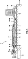
- FIG. 1 shows a cross section through a first embodiment of the invention.
- the electrical control device 1 comprises a printed circuit substrate 2. This may be formed as a single-layer printed circuit board or multilayer printed circuit board or as a flexible printed circuit foil laminated on a metal plate or as an injection molded part with interconnects embedded therein or in any other way.
- the interconnect substrate is formed substantially plate-shaped with a first side 15 and a second side facing away from 16 and a peripheral end face 31.
- the conductor substrate 2 is provided in a locally limited area with electrical components 11 which form an electronic circuit 9.
- the components 11 can also be applied only on one side of the conductor substrate.
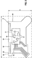
- the area equipped with the components 11 is in FIG.
- the electrical components 11 are electrically connected to each other by conductor tracks 12 of the conductor substrate 2.
- the conductor tracks may be guided over one or more layers of the multi-layer substrate.
- further printed conductors 13 and printed conductors 14 are arranged on the printed conductor substrate which lead to remote regions of the printed conductor substrate 2 outside the area occupied by the electronic circuit 9 on the first side 15 and the second side 16.
- the interconnect substrate has a maximum length a and a maximum width b, which are sized so that the least possible material waste.
- the areal extent of the conductor substrate 2 is adapted to the conditions in a motor vehicle transmission. As in FIG.
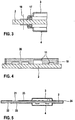
- the housing parts 3, 4 may be formed, for example, as metallic half-shell parts, for example as stamped and bent parts. How best in FIG. 3 can be seen, the first housing part 3 and the second housing part 4 may be angled several times in the edge region in a known manner, so that in each case a circumferential sealing ring 17 between the angled portion of the respective housing part and the conductor substrate 2 can be arranged.
- first housing part 3 and the second housing part 4 are fixed to the conductor substrate 2, wherein the respective circumferential sealing ring 17 between the associated housing part and the conductor substrate 2 is compressed and the electronic circuit 9 is sealed to the outside.
- the interconnects 14 of the interconnect substrate 2 connect the electrical components 11 to a device connector part 6, which is arranged outside the area covered by the housing parts 3, 4 on the interconnect substrate.
- the device connector part 6 serves to connect the control unit 1 to an external wiring harness. It is important that outside of the area covered by the housing parts 3, 4 and outside of the area covered by the device connector part 6 on the conductor substrate 2 at least one contact point 21 is arranged, which serves for contacting a further electrical component of the control unit.
- the at least one contact point 21 may be formed, for example, in the form of a metallized surface or a via.
- the further component can be, for example, a sensor connection part 7.
- the sensor connection part 7 is used for connection to a rotational speed sensor and is electrically connected by means of two contact pins 30 with two contact points 21 on the conductor track substrate.
- the contact points 21 are connected via printed conductors 13 to the electronic circuit 9, as shown in FIG FIG. 2 is shown.
- the sensor connection part 7 can be mechanically fastened to the conductor substrate 2 outside the area covered by the housing parts 3, 4 and the device plug part.
- at least one further contact point 22, which is connected by means of an electrically conductive spring contact element 29 to an electrohydraulic actuator, is arranged on the second side of the conductor substrate.
- the electro-hydraulic actuator 8 may be, for example, a pressure regulating valve that regulates the hydraulic pressure in a hydraulic line of the transmission.
- the contacting of the contact points with the electrical components can be done by means of plug contacts, solder contacts, press-in contacts, spring contacts or in any other suitable manner. All contact points are connected via interconnects of the interconnect substrate to the electronic circuit 9.
- the printed circuit substrate 2 equipped with the housing parts 3, 4, the device connector part 6 and the contact points 21, 22 and optionally electrical components 7 is mounted with a flat outer surface of the second housing part 4 on a heat sink 10, which is, for example, the hydraulic plate of a transmission can act.
- a heat sink 10 which is, for example, the hydraulic plate of a transmission can act.
- a plurality of actuators 8 are fixed, which are connected via spring contact elements 29 with associated contact points 22 on the interconnect substrate electrical.
- a filled with a potting compound 20 frame member 19 can be used as a housing part for covering the electrical components 11.
- the components 11 covering housing parts by Moldmassen, foams, gels or in any other way. It is important that the components 11 on the first side 15 and the components 11 on the second side 16 are protected by the housing parts 3, 4 from aggressive media.
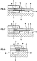
- FIG. 5 A particularly preferred embodiment of the invention is in FIG. 5 shown.
- This embodiment differs from that in FIG. 1 illustrated embodiment in that the not covered by the housing parts 3, 4 areas on the first side 15 and the second side 16 of the conductor substrate 2 are provided with a protective coating.
- the protective layer 23 preferably comprises a large copper conductor track, a paint or a suitable hard or soft coating, which prevents the diffusion of media such as gear oil or moist air into the substrate.
- an edge cover 24 is applied as a protective coating.
- the edge cover 24 may be realized by means of lacquers, molding compounds, encapsulation or another suitable passivation.
- the heat dissipation of heat generating devices 11 can be made in various ways. As in Fig. 6 1, the heat generated by power components 11 on the first side 15 of the conductor substrate 2 can be dissipated to the second side 16, for example in a manner known per se, via plated-through holes 25 provided in the conductor substrate.
- the second side 16 of the conductor substrate 2 is in thermal contact with a waveguide layer 26.
- the heat-conducting layer 26 may be, for example, a copper layer which transfers the heat to the housing part 4 which is in heat-conducting contact therewith. From there, the heat flows to a heat sink 10, on which the housing part 4 rests and which, for example, constitutes a hydraulic plate of the transmission.
- the heat can also be transferred directly from the heat-conducting layer 26 to the heat sink 10.
- the heat sink may be provided with a pedestal 27 on which the conductor substrate 2 rests with the interposition of the heat-conducting layer 26.
- the heat sink 10 also have a recess 32 and a recess 32 surrounding edge 28, on which the conductor substrate 2 rests with the interposition of the heat-conducting layer 26.
Claims (7)
- Module (1) de commande de transmission, présentant
un substrat (2) de pistes conductrices sur lequel est disposé un circuit électronique (9) qui comporte plusieurs composants électriques (11) reliés les uns aux autres par des pistes conductrices (12, 13, 14) du substrat de pistes conductrices,
au moins une partie (3, 4) de boîtier qui recouvre les composants électriques (11) placés sur le substrat de pistes conductrices et
au moins une partie (6) de fiche d'appareil reliée électriquement aux composants et disposée sur le substrat (2) de pistes conductrices à l'extérieur de la partie du substrat de pistes conductrices recouverte par la ou les parties (3, 4) de boîtier,
les liaisons électriques entre les composants et la partie de fiche d'appareil s'effectuant par des pistes conductrices (14) du substrat de pistes conductrices et au moins un emplacement de contact (21, 22) prévu pour un autre composant électrique (7, 8) étant disposé sur le substrat (2) de pistes conductrices à l'extérieur de la partie du substrat de pistes conductrices recouverte par la ou les parties (3, 4) de boîtier et à l'extérieur de la partie du substrat (2) de pistes conductrices dotée de la partie (6) de fiche d'appareil,
le substrat (2) de pistes conductrices étant une carte de circuit multicouche dont les pistes conductrices (14) traversent plusieurs couches des parties extérieures non recouvertes par la ou les parties (3, 4) de boîtier et la partie (6) de fiche d'appareil et le ou les emplacements de contact (21, 22) de la carte (2) de circuit multicouche étant dotés d'un revêtement protecteur (23, 24) qui empêche la diffusion d'huile de transmission, d'eau et d'autres fluides nocifs,
la carte de circuit multicouche présentant la forme d'une plaque dotée d'une première face (15) et d'une deuxième face (16) non tournée vers la première face ainsi que d'un côté frontal périphérique (31), caractérisé en ce que
le revêtement de protection (23, 24) comporte une couche de protection (23) appliquée sur la première face et la deuxième face et un recouvrement de champ (24) appliqué sur le côté frontal périphérique. - Module (1) de commande de transmission selon la revendication 1, caractérisé en ce que l'autre composant électrique (7) est disposé sur la carte (2) de circuit multicouche.
- Module (1) de commande de transmission selon la revendication 1, caractérisé en ce que le revêtement de protection (23, 24) comporte une couche de cuivre, un vernis ou une autre couche de passivation appropriée.
- Module (1) de commande de transmission selon la revendication 1, caractérisé en ce que le ou les emplacements de contact (21) sont reliés électriquement à une pièce (7) de raccordement de détecteur appliquée sur la carte (2) de circuit multicouche ou en ce que le ou les emplacements de contact (22) sont reliés électriquement à un actionneur électrohydraulique (8).
- Module (1) de commande de transmission selon la revendication 1, caractérisé en ce qu'au moins une partie (4) de boîtier est configurée avec une surface destinée à être posée sur un corps de refroidissement (10) prévu pour évacuer la chaleur, en particulier sur une plaque hydraulique d'une transmission de véhicule automobile.
- Module (1) de commande de transmission selon la revendication 1, caractérisé en ce qu'au moins un composant électrique (11) disposé sur une autre face (15) du substrat (2) de pistes conductrices et dégageant de la chaleur est relié thermiquement par des perforations de contact (25) du substrat (2) de pistes conductrices à une couche (26) conduisant la chaleur située sur une deuxième face (16) du substrat de pistes conductrices non tournée vers la première face.
- Module (1) de commande de transmission selon la revendication 6, caractérisé en ce que la couche (26) thermiquement conductrice est en contact de conduction thermique avec une partie (3, 4) de boîtier et/ou avec un corps de refroidissement (10).
Priority Applications (1)
| Application Number | Priority Date | Filing Date | Title |
|---|---|---|---|
| EP10181790A EP2273859A3 (fr) | 2007-06-28 | 2008-05-13 | Utilisation d'un module de commande pour une commande d'engrenage insérée dans une boîte de vitesse automatique |
Applications Claiming Priority (2)
| Application Number | Priority Date | Filing Date | Title |
|---|---|---|---|
| DE102007029913A DE102007029913A1 (de) | 2007-06-28 | 2007-06-28 | Elektrisches Steuergerät |
| PCT/EP2008/055811 WO2009000594A1 (fr) | 2007-06-28 | 2008-05-13 | Unité de commande électrique |
Related Child Applications (2)
| Application Number | Title | Priority Date | Filing Date |
|---|---|---|---|
| EP10181790A Division-Into EP2273859A3 (fr) | 2007-06-28 | 2008-05-13 | Utilisation d'un module de commande pour une commande d'engrenage insérée dans une boîte de vitesse automatique |
| EP10181790.6 Division-Into | 2010-09-29 |
Publications (3)
| Publication Number | Publication Date |
|---|---|
| EP2163148A1 EP2163148A1 (fr) | 2010-03-17 |
| EP2163148B1 EP2163148B1 (fr) | 2013-07-17 |
| EP2163148B2 true EP2163148B2 (fr) | 2017-01-11 |
Family
ID=39790276
Family Applications (2)
| Application Number | Title | Priority Date | Filing Date |
|---|---|---|---|
| EP10181790A Withdrawn EP2273859A3 (fr) | 2007-06-28 | 2008-05-13 | Utilisation d'un module de commande pour une commande d'engrenage insérée dans une boîte de vitesse automatique |
| EP08759525.2A Not-in-force EP2163148B2 (fr) | 2007-06-28 | 2008-05-13 | Unité de commande électrique |
Family Applications Before (1)
| Application Number | Title | Priority Date | Filing Date |
|---|---|---|---|
| EP10181790A Withdrawn EP2273859A3 (fr) | 2007-06-28 | 2008-05-13 | Utilisation d'un module de commande pour une commande d'engrenage insérée dans une boîte de vitesse automatique |
Country Status (8)
| Country | Link |
|---|---|
| US (2) | US8488324B2 (fr) |
| EP (2) | EP2273859A3 (fr) |
| JP (2) | JP5393663B2 (fr) |
| KR (1) | KR101484799B1 (fr) |
| CN (2) | CN102595813B (fr) |
| DE (1) | DE102007029913A1 (fr) |
| ES (1) | ES2425372T5 (fr) |
| WO (1) | WO2009000594A1 (fr) |
Families Citing this family (54)
| Publication number | Priority date | Publication date | Assignee | Title |
|---|---|---|---|---|
| DE102007029913A1 (de) * | 2007-06-28 | 2009-01-02 | Robert Bosch Gmbh | Elektrisches Steuergerät |
| DE102007032535B4 (de) | 2007-07-12 | 2009-09-24 | Continental Automotive Gmbh | Elektronisches Modul für eine integrierte mechatronische Getriebesteuerung |
| DE102008040501A1 (de) * | 2008-07-17 | 2010-01-21 | Robert Bosch Gmbh | Verbesserte Wärmeabfuhr aus einem Steuergerät |
| DE102009054585A1 (de) * | 2009-12-14 | 2011-06-16 | Robert Bosch Gmbh | Steuergerät |
| US8189336B2 (en) * | 2010-01-22 | 2012-05-29 | GM Global Technology Operations LLC | Composite cover with integral heat sink |
| DE102010030525A1 (de) * | 2010-06-25 | 2011-12-29 | Zf Friedrichshafen Ag | Elektronische Steuerbaugruppe |
| DE102010030891A1 (de) * | 2010-07-02 | 2012-01-05 | Zf Friedrichshafen Ag | Steuergerätbaugruppe |
| DE102010026953B4 (de) * | 2010-07-12 | 2015-02-26 | Continental Automotive Gmbh | Gehäuse einer elektronischen Schaltung für eine Kraftstoffpumpe |
| DE102010039550A1 (de) * | 2010-08-20 | 2012-02-23 | Zf Friedrichshafen Ag | Steuermodul |
| WO2012032789A1 (fr) * | 2010-09-09 | 2012-03-15 | 株式会社オートネットワーク技術研究所 | Unité de circuit électronique à monter sur une transmission automatique de véhicule et son procédé de fabrication |
| DE102010062653A1 (de) | 2010-12-08 | 2012-06-14 | Robert Bosch Gmbh | Steuermodul und Verfahren zu seiner Herstellung |
| DE102011015912B4 (de) * | 2011-04-01 | 2022-03-17 | Sew-Eurodrive Gmbh & Co Kg | Anordnung zum Temperieren für Wärme erzeugende elektrische Bauteile und Verfahren zum Herstellen einer Kühlanordnung für elektrische Bauteile |
| DE102011007300A1 (de) * | 2011-04-13 | 2012-10-18 | Zf Friedrichshafen Ag | Steuergerät für ein Getriebe eines Fahrzeugs und Verfahren zur Montage eines Steuergeräts für ein Getriebe eines Fahrzeugs an einem Getriebeelement |
| US8966747B2 (en) * | 2011-05-11 | 2015-03-03 | Vlt, Inc. | Method of forming an electrical contact |
| DE102011082537A1 (de) * | 2011-09-12 | 2013-03-14 | Robert Bosch Gmbh | Leiterplatte und elektrische Bauteile zum Einsatz in aggressiver Umgebung und Verfahren zur Herstellung einer solchen Leiterplatte |
| DE102011083620A1 (de) * | 2011-09-28 | 2013-03-28 | Zf Friedrichshafen Ag | Leiterplatte für ein Steuergerät, Steuergerät und Verfahren zur Montage eines Steuergeräts |
| DE102011085169A1 (de) | 2011-10-25 | 2013-04-25 | Robert Bosch Gmbh | Steuergerät für ein Kraftfahrzeug |
| DE102011085629A1 (de) | 2011-11-02 | 2013-05-02 | Robert Bosch Gmbh | Elektronikmodul zum Betrieb im Getriebe |
| DE102011085650B4 (de) * | 2011-11-03 | 2022-09-01 | Robert Bosch Gmbh | Befestigung eines Steuergerätes für ein Getriebesteuermodul an einer Trägerplatte |
| DE102011088969A1 (de) | 2011-12-19 | 2013-06-20 | Robert Bosch Gmbh | Getriebesteuermodul |
| DE102011089474A1 (de) * | 2011-12-21 | 2013-06-27 | Robert Bosch Gmbh | Elektronikmodul für ein Fahrzeug |
| DE102012000907A1 (de) * | 2012-01-19 | 2013-07-25 | Sew-Eurodrive Gmbh & Co. Kg | Elektrogerät |
| DE102012207057A1 (de) | 2012-04-27 | 2013-10-31 | Robert Bosch Gmbh | Vorrichtung mit einem zwischen einem ersten Bauteil und einem zweiten Bauteil angeordneten elastischen Dichtungsteil und Verfahren zur Herstellung einer solchen Vorrichtung |
| DE102012213917A1 (de) * | 2012-08-06 | 2014-02-20 | Robert Bosch Gmbh | Bauelemente-Ummantelung für ein Elektronikmodul |
| DE102012215673A1 (de) * | 2012-09-04 | 2014-03-06 | Zf Friedrichshafen Ag | Anordnung eines elektrischen Steuergeräts an eine Schaltplatte |
| JP5983317B2 (ja) * | 2012-11-01 | 2016-08-31 | 住友電気工業株式会社 | ケーブル付電子機器およびその組立方法 |
| DE102013212254A1 (de) * | 2013-06-26 | 2014-12-31 | Robert Bosch Gmbh | MID-Bauteil, Verfahren zur Herstellung |
| DE102013212446A1 (de) * | 2013-06-27 | 2015-01-15 | Zf Friedrichshafen Ag | Elektrische Schaltung und Verfahren zum Herstellen einer elektrischen Schaltung zur Ansteuerung einer Last |
| DE102013010843A1 (de) | 2013-06-28 | 2014-12-31 | Wabco Gmbh | Elektrisches Steuergerät |
| DE102013215149A1 (de) * | 2013-08-01 | 2015-02-19 | Conti Temic Microelectronic Gmbh | Mehrstufiges Dichtsystem zum Einsatz in einem Kraftfahrzeugsteuergerät |
| US9385059B2 (en) * | 2013-08-28 | 2016-07-05 | Infineon Technologies Ag | Overmolded substrate-chip arrangement with heat sink |
| DE102013221110A1 (de) | 2013-10-17 | 2015-04-23 | Zf Friedrichshafen Ag | Steuerungseinrichtung |
| DE102013221120A1 (de) | 2013-10-17 | 2015-04-23 | Zf Friedrichshafen Ag | Steuerungseinrichtung |
| JP6357878B2 (ja) * | 2014-05-28 | 2018-07-18 | 株式会社デンソー | 電子装置 |
| DE102014214057A1 (de) * | 2014-07-18 | 2016-01-21 | Zf Friedrichshafen Ag | Elektronische Getriebesteuerungseinrichtung und Verfahren zum Herstellen derselben |
| DE102014217351A1 (de) * | 2014-08-29 | 2016-03-03 | Robert Bosch Gmbh | Modulanordnung sowie Getriebesteuermodul |
| JP6330686B2 (ja) * | 2015-02-18 | 2018-05-30 | 株式会社オートネットワーク技術研究所 | 基板ユニット |
| US9293870B1 (en) * | 2015-03-10 | 2016-03-22 | Continental Automotive Systems, Inc. | Electronic control module having a cover allowing for inspection of right angle press-fit pins |
| DE102015012740A1 (de) | 2015-10-01 | 2017-04-06 | Wabco Gmbh | Fahrzeugsteuergerät |
| DE102015220473B4 (de) | 2015-10-21 | 2024-02-22 | Bayerische Motoren Werke Aktiengesellschaft | Verfahren zum Herstellen eines Gehäusebauteils mit Schirmung vor elektromagnetischer Strahlung und mit Umweltdichtungsfunktion |
| DE102015221149A1 (de) * | 2015-10-29 | 2017-05-04 | Robert Bosch Gmbh | Steuervorrichtung für eine Getriebesteuerung eines Kraftfahrzeugs |
| US9807905B2 (en) * | 2015-11-25 | 2017-10-31 | General Electric Company | Adapter cooling apparatus and method for modular computing devices |
| DE102015223394A1 (de) * | 2015-11-26 | 2017-06-01 | Zf Friedrichshafen Ag | Einzelmodul und Modulanordnung |
| DE102016205966A1 (de) * | 2016-04-11 | 2017-10-12 | Zf Friedrichshafen Ag | Elektronische Einheit mit ESD-Schutzanordnung |
| DE102016217554A1 (de) * | 2016-09-14 | 2018-03-15 | Robert Bosch Gmbh | Elektronische Baugruppe, insbesondere für ein Getriebesteuermodul, und Verfahren zum Herstellen einer elektronischen Baugruppe |
| DE102016219116A1 (de) * | 2016-09-30 | 2018-04-05 | Robert Bosch Gmbh | Verfahren zum Herstellen einer elektronischen Baugruppe und elektronische Baugruppe, insbesondere für ein Getriebesteuermodul |
| DE102016225025A1 (de) | 2016-12-14 | 2018-06-14 | Robert Bosch Gmbh | Getriebesteuermodul zur Ansteuerung eines Kraftfahrzeuggetriebes |
| DE102016225029A1 (de) | 2016-12-14 | 2018-06-14 | Robert Bosch Gmbh | Getriebesteuermodul zur Ansteuerung eines Kraftfahrzeuggetriebes und Verfahren zur Herstellung eines Getriebesteuermoduls |
| JP6888434B2 (ja) * | 2017-06-16 | 2021-06-16 | 株式会社オートネットワーク技術研究所 | 回路ユニット |
| WO2019065423A1 (fr) * | 2017-09-29 | 2019-04-04 | アイシン・エィ・ダブリュ株式会社 | Dispositif d'entraînement pour véhicules |
| JP2019103205A (ja) * | 2017-11-30 | 2019-06-24 | 日本電産株式会社 | 回路基板、モータ、及びファンモータ |
| DE102019202036A1 (de) * | 2019-02-15 | 2020-08-20 | Zf Friedrichshafen Ag | Prozessoptimiertte und strukturoptimierte Kontaktierung von Leistungsmodulen an einem Kühlkörper |
| DE102019219478A1 (de) | 2019-12-12 | 2021-06-17 | Continental Automotive Gmbh | Modular erweiterbares elektronisches steuergerät |
| DE102020207871A1 (de) * | 2020-06-25 | 2021-12-30 | Robert Bosch Gesellschaft mit beschränkter Haftung | Elektronische Anordnung |
Family Cites Families (33)
| Publication number | Priority date | Publication date | Assignee | Title |
|---|---|---|---|---|
| US4328407A (en) | 1980-01-04 | 1982-05-04 | Conergy Associates | Heating system and control |
| DE3040460C2 (de) | 1980-10-27 | 1982-12-16 | Siemens AG, 1000 Berlin und 8000 München | Elektronische Schaltung und Verfahren zu ihrer Herstellung |
| DE3114061C2 (de) | 1981-04-07 | 1984-04-12 | ANT Nachrichtentechnik GmbH, 7150 Backnang | Verfahren zur Herstellung von durchkontaktierten gedruckten Schaltungen |
| US4628407A (en) | 1983-04-22 | 1986-12-09 | Cray Research, Inc. | Circuit module with enhanced heat transfer and distribution |
| US4535385A (en) * | 1983-04-22 | 1985-08-13 | Cray Research, Inc. | Circuit module with enhanced heat transfer and distribution |
| US4894018A (en) * | 1988-08-08 | 1990-01-16 | General Motors Corporation | Low profile electrical connector |
| DE3885457D1 (de) | 1988-08-25 | 1993-12-09 | Siemens Nixdorf Inf Syst | Verfahren zum Herstellen von durchkontaktierten Leiterplatten mit sehr kleinen oder keinen Löträndern um die Durchkontaktierungslöcher. |
| DE3843787A1 (de) | 1988-12-24 | 1990-07-05 | Standard Elektrik Lorenz Ag | Verfahren und leiterplatte zum montieren eines halbleiter-bauelements |
| DE4023319C1 (fr) | 1990-07-21 | 1991-12-12 | Robert Bosch Gmbh, 7000 Stuttgart, De | |
| SE469320B (sv) * | 1990-11-02 | 1993-06-21 | Thams Johan Petter B | Foerfarande foer belaeggning av moensterkort med en lackbelaeggning, speciellt en loedmask |
| JPH0530037A (ja) | 1991-07-23 | 1993-02-05 | Matsushita Electric Ind Co Ltd | 光双方向通信装置 |
| DE4232575A1 (de) * | 1992-09-29 | 1994-03-31 | Bosch Gmbh Robert | Anordnung mit einer Leiterplatte, mindestens einem Leistungsbauelement und einem Kühlkörper |
| DE4335946C2 (de) | 1993-10-21 | 1997-09-11 | Bosch Gmbh Robert | Anordnung bestehend aus einer Leiterplatte |
| DE19528632A1 (de) * | 1995-08-04 | 1997-02-06 | Bosch Gmbh Robert | Steuergerät bestehend aus mindestens zwei Gehäuseteilen |
| FR2740608B1 (fr) | 1995-10-25 | 1997-12-19 | Giat Ind Sa | Procede pour deposer un revetement de protection sur les composants d'une carte electronique |
| JP3300254B2 (ja) | 1997-04-28 | 2002-07-08 | 矢崎総業株式会社 | 樹脂被覆実装基板及びその製造方法 |
| US6195267B1 (en) * | 1999-06-23 | 2001-02-27 | Ericsson Inc. | Gel structure for combined EMI shielding and thermal control of microelectronic assemblies |
| JP4027558B2 (ja) | 2000-03-03 | 2007-12-26 | 三菱電機株式会社 | パワーモジュール |
| DE60135405D1 (de) * | 2000-03-21 | 2008-10-02 | Autonetworks Technologies Ltd | Leistungsverteiler für ein Kraftfahrzeug und Verfahren zur Herstellung dazu |
| JP3814467B2 (ja) | 2000-06-28 | 2006-08-30 | 株式会社日立製作所 | 車両用電子制御装置 |
| DE10110257A1 (de) * | 2001-03-02 | 2002-09-19 | Siemens Ag | Mechatronische Getriebeanordnung für Kraftfahrzeuge |
| JP3770157B2 (ja) * | 2001-12-26 | 2006-04-26 | 株式会社デンソー | 電子制御機器 |
| JP2003198078A (ja) | 2001-12-28 | 2003-07-11 | Nidec Copal Corp | プリント配線基板及びその製造方法 |
| CN1208998C (zh) * | 2002-03-08 | 2005-06-29 | 启亨股份有限公司 | 印刷电路板及其制作方法 |
| JP3910497B2 (ja) * | 2002-07-03 | 2007-04-25 | 株式会社オートネットワーク技術研究所 | 電力回路部の防水方法及び電力回路部をもつパワーモジュール |
| JP2004303860A (ja) | 2003-03-31 | 2004-10-28 | Mitsumi Electric Co Ltd | 電子部品の放熱構造 |
| DE102004061818A1 (de) | 2004-12-22 | 2006-07-06 | Robert Bosch Gmbh | Steuermodul |
| JP4473141B2 (ja) * | 2005-01-04 | 2010-06-02 | 日立オートモティブシステムズ株式会社 | 電子制御装置 |
| DE102005002813B4 (de) * | 2005-01-20 | 2006-10-19 | Robert Bosch Gmbh | Steuermodul |
| DE102005015717A1 (de) * | 2005-03-31 | 2006-10-05 | Robert Bosch Gmbh | Elektrische Schaltungsanordung |
| DE102005022536A1 (de) | 2005-05-17 | 2006-11-23 | Siemens Ag | Steuereinheit mit einer flexiblen Leiterplatte |
| DE102007029913A1 (de) * | 2007-06-28 | 2009-01-02 | Robert Bosch Gmbh | Elektrisches Steuergerät |
| DE102010062653A1 (de) * | 2010-12-08 | 2012-06-14 | Robert Bosch Gmbh | Steuermodul und Verfahren zu seiner Herstellung |
-
2007
- 2007-06-28 DE DE102007029913A patent/DE102007029913A1/de not_active Withdrawn
-
2008
- 2008-05-13 WO PCT/EP2008/055811 patent/WO2009000594A1/fr active Application Filing
- 2008-05-13 ES ES08759525.2T patent/ES2425372T5/es active Active
- 2008-05-13 KR KR1020097027062A patent/KR101484799B1/ko not_active IP Right Cessation
- 2008-05-13 CN CN201210020338.4A patent/CN102595813B/zh not_active Expired - Fee Related
- 2008-05-13 US US12/452,126 patent/US8488324B2/en active Active
- 2008-05-13 CN CN2008800219280A patent/CN101690437B/zh active Active
- 2008-05-13 JP JP2010513811A patent/JP5393663B2/ja not_active Expired - Fee Related
- 2008-05-13 EP EP10181790A patent/EP2273859A3/fr not_active Withdrawn
- 2008-05-13 EP EP08759525.2A patent/EP2163148B2/fr not_active Not-in-force
-
2012
- 2012-06-06 US US13/490,245 patent/US9345139B2/en not_active Expired - Fee Related
-
2013
- 2013-08-15 JP JP2013168993A patent/JP6016731B2/ja not_active Expired - Fee Related
Also Published As
| Publication number | Publication date |
|---|---|
| DE102007029913A1 (de) | 2009-01-02 |
| EP2163148B1 (fr) | 2013-07-17 |
| JP5393663B2 (ja) | 2014-01-22 |
| CN102595813A (zh) | 2012-07-18 |
| US8488324B2 (en) | 2013-07-16 |
| JP2010531632A (ja) | 2010-09-24 |
| US9345139B2 (en) | 2016-05-17 |
| KR101484799B1 (ko) | 2015-01-20 |
| US20120240396A1 (en) | 2012-09-27 |
| WO2009000594A1 (fr) | 2008-12-31 |
| US20100202110A1 (en) | 2010-08-12 |
| ES2425372T3 (es) | 2013-10-15 |
| EP2163148A1 (fr) | 2010-03-17 |
| ES2425372T5 (es) | 2017-07-05 |
| EP2273859A2 (fr) | 2011-01-12 |
| CN101690437B (zh) | 2013-07-24 |
| JP2014013079A (ja) | 2014-01-23 |
| EP2273859A3 (fr) | 2012-05-02 |
| CN101690437A (zh) | 2010-03-31 |
| KR20100029777A (ko) | 2010-03-17 |
| JP6016731B2 (ja) | 2016-10-26 |
| CN102595813B (zh) | 2015-11-25 |
Similar Documents
| Publication | Publication Date | Title |
|---|---|---|
| EP2163148B2 (fr) | Unité de commande électrique | |
| EP2796016B1 (fr) | Module de commande de boîte de vitesses | |
| EP1239710B1 (fr) | Ensemble électronique | |
| EP1648744B1 (fr) | Bloc electronique et procede de fabrication d'un bloc electronique | |
| EP2649869B1 (fr) | Module de contrôle et méthode pour sa préparation | |
| WO2014094754A1 (fr) | Module électronique contenant un circuit électronique enrobé de matière plastique et procédé pour le fabriquer | |
| EP3369296B1 (fr) | Unité de commande pour commande de boîte de vitesses d'un vehicule automobile | |
| EP2055155B1 (fr) | Appareil de commande pour vehicule automobile | |
| DE102007019098B4 (de) | Modul für eine integrierte Steuerelektronik mit vereinfachtem Aufbau | |
| EP2188839B1 (fr) | Méthode de fabrication d'un dispositif de refroidissement pour un circuit électronique avec des semiconducteurs de puissance générant de la chaleur | |
| DE102015218706B4 (de) | Elektronische Komponente | |
| DE102007039618B4 (de) | Modul für eine integrierte Steuerelektronik mit vereinfachtem Aufbau | |
| EP2964979B1 (fr) | Système d'étanchéité en plusieurs parties destiné à être utilisé dans un appareil de commande de véhicule automobile | |
| EP2671431B1 (fr) | Ensemble carte de circuit imprimé | |
| WO2017054981A1 (fr) | Module électronique pour un appareil de commande de transmission | |
| DE102017206217A1 (de) | Elektrische Kontaktanordnung | |
| EP1057384A1 (fr) | Appareil de commande electronique | |
| WO2018069069A1 (fr) | Procédé pour réaliser au moins un chemin de dissipation de chaleur pour un composant microélectronique et composant microélectronique correspondant | |
| DE102006029711B4 (de) | Trägervorrichtung | |
| DE102006052458B4 (de) | Elektronikgehäuse mit neuer flexibler Leiterplattentechnologie | |
| DE102020202189A1 (de) | Leiterplattenanordnung, Getriebesteuergerät mit einer Leiterplattenanordnung und Verwendung der Leiterplattenanordnung in einem Getriebesteuergerät | |
| DE102020216389A1 (de) | Anordnung einer Leiterplatte an eine Schnittstelle | |
| EP4211996A1 (fr) | Procédé et système de production de pièce coulée pour la production d'un carter de moteur électrique, et moteur électrique | |
| WO2012022535A1 (fr) | Module de commande |
Legal Events
| Date | Code | Title | Description |
|---|---|---|---|
| PUAI | Public reference made under article 153(3) epc to a published international application that has entered the european phase |
Free format text: ORIGINAL CODE: 0009012 |
|
| 17P | Request for examination filed |
Effective date: 20100128 |
|
| AK | Designated contracting states |
Kind code of ref document: A1 Designated state(s): AT BE BG CH CY CZ DE DK EE ES FI FR GB GR HR HU IE IS IT LI LT LU LV MC MT NL NO PL PT RO SE SI SK TR |
|
| AX | Request for extension of the european patent |
Extension state: AL BA MK RS |
|
| DAX | Request for extension of the european patent (deleted) | ||
| 17Q | First examination report despatched |
Effective date: 20101012 |
|
| GRAP | Despatch of communication of intention to grant a patent |
Free format text: ORIGINAL CODE: EPIDOSNIGR1 |
|
| RIC1 | Information provided on ipc code assigned before grant |
Ipc: H05K 3/28 20060101ALI20121116BHEP Ipc: H05K 7/20 20060101ALI20121116BHEP Ipc: H05K 1/18 20060101ALI20121116BHEP Ipc: H05K 5/00 20060101AFI20121116BHEP |
|
| GRAS | Grant fee paid |
Free format text: ORIGINAL CODE: EPIDOSNIGR3 |
|
| GRAA | (expected) grant |
Free format text: ORIGINAL CODE: 0009210 |
|
| AK | Designated contracting states |
Kind code of ref document: B1 Designated state(s): AT BE BG CH CY CZ DE DK EE ES FI FR GB GR HR HU IE IS IT LI LT LU LV MC MT NL NO PL PT RO SE SI SK TR |
|
| REG | Reference to a national code |
Ref country code: GB Ref legal event code: FG4D Free format text: NOT ENGLISH |
|
| REG | Reference to a national code |
Ref country code: CH Ref legal event code: EP |
|
| REG | Reference to a national code |
Ref country code: IE Ref legal event code: FG4D Free format text: LANGUAGE OF EP DOCUMENT: GERMAN |
|
| REG | Reference to a national code |
Ref country code: AT Ref legal event code: REF Ref document number: 622850 Country of ref document: AT Kind code of ref document: T Effective date: 20130815 |
|
| REG | Reference to a national code |
Ref country code: DE Ref legal event code: R096 Ref document number: 502008010327 Country of ref document: DE Effective date: 20130912 |
|
| REG | Reference to a national code |
Ref country code: ES Ref legal event code: FG2A Ref document number: 2425372 Country of ref document: ES Kind code of ref document: T3 Effective date: 20131015 |
|
| REG | Reference to a national code |
Ref country code: NL Ref legal event code: VDEP Effective date: 20130717 |
|
| REG | Reference to a national code |
Ref country code: LT Ref legal event code: MG4D |
|
| PG25 | Lapsed in a contracting state [announced via postgrant information from national office to epo] |
Ref country code: IS Free format text: LAPSE BECAUSE OF FAILURE TO SUBMIT A TRANSLATION OF THE DESCRIPTION OR TO PAY THE FEE WITHIN THE PRESCRIBED TIME-LIMIT Effective date: 20131117 Ref country code: NO Free format text: LAPSE BECAUSE OF FAILURE TO SUBMIT A TRANSLATION OF THE DESCRIPTION OR TO PAY THE FEE WITHIN THE PRESCRIBED TIME-LIMIT Effective date: 20131017 Ref country code: LT Free format text: LAPSE BECAUSE OF FAILURE TO SUBMIT A TRANSLATION OF THE DESCRIPTION OR TO PAY THE FEE WITHIN THE PRESCRIBED TIME-LIMIT Effective date: 20130717 Ref country code: SE Free format text: LAPSE BECAUSE OF FAILURE TO SUBMIT A TRANSLATION OF THE DESCRIPTION OR TO PAY THE FEE WITHIN THE PRESCRIBED TIME-LIMIT Effective date: 20130717 Ref country code: CY Free format text: LAPSE BECAUSE OF FAILURE TO SUBMIT A TRANSLATION OF THE DESCRIPTION OR TO PAY THE FEE WITHIN THE PRESCRIBED TIME-LIMIT Effective date: 20130821 Ref country code: PT Free format text: LAPSE BECAUSE OF FAILURE TO SUBMIT A TRANSLATION OF THE DESCRIPTION OR TO PAY THE FEE WITHIN THE PRESCRIBED TIME-LIMIT Effective date: 20131118 Ref country code: HR Free format text: LAPSE BECAUSE OF FAILURE TO SUBMIT A TRANSLATION OF THE DESCRIPTION OR TO PAY THE FEE WITHIN THE PRESCRIBED TIME-LIMIT Effective date: 20130717 |
|
| PG25 | Lapsed in a contracting state [announced via postgrant information from national office to epo] |
Ref country code: LV Free format text: LAPSE BECAUSE OF FAILURE TO SUBMIT A TRANSLATION OF THE DESCRIPTION OR TO PAY THE FEE WITHIN THE PRESCRIBED TIME-LIMIT Effective date: 20130717 Ref country code: SI Free format text: LAPSE BECAUSE OF FAILURE TO SUBMIT A TRANSLATION OF THE DESCRIPTION OR TO PAY THE FEE WITHIN THE PRESCRIBED TIME-LIMIT Effective date: 20130717 Ref country code: PL Free format text: LAPSE BECAUSE OF FAILURE TO SUBMIT A TRANSLATION OF THE DESCRIPTION OR TO PAY THE FEE WITHIN THE PRESCRIBED TIME-LIMIT Effective date: 20130717 Ref country code: FI Free format text: LAPSE BECAUSE OF FAILURE TO SUBMIT A TRANSLATION OF THE DESCRIPTION OR TO PAY THE FEE WITHIN THE PRESCRIBED TIME-LIMIT Effective date: 20130717 Ref country code: GR Free format text: LAPSE BECAUSE OF FAILURE TO SUBMIT A TRANSLATION OF THE DESCRIPTION OR TO PAY THE FEE WITHIN THE PRESCRIBED TIME-LIMIT Effective date: 20131018 Ref country code: NL Free format text: LAPSE BECAUSE OF FAILURE TO SUBMIT A TRANSLATION OF THE DESCRIPTION OR TO PAY THE FEE WITHIN THE PRESCRIBED TIME-LIMIT Effective date: 20130717 |
|
| PG25 | Lapsed in a contracting state [announced via postgrant information from national office to epo] |
Ref country code: CY Free format text: LAPSE BECAUSE OF FAILURE TO SUBMIT A TRANSLATION OF THE DESCRIPTION OR TO PAY THE FEE WITHIN THE PRESCRIBED TIME-LIMIT Effective date: 20130717 |
|
| PLBI | Opposition filed |
Free format text: ORIGINAL CODE: 0009260 |
|
| PG25 | Lapsed in a contracting state [announced via postgrant information from national office to epo] |
Ref country code: RO Free format text: LAPSE BECAUSE OF FAILURE TO SUBMIT A TRANSLATION OF THE DESCRIPTION OR TO PAY THE FEE WITHIN THE PRESCRIBED TIME-LIMIT Effective date: 20130717 Ref country code: SK Free format text: LAPSE BECAUSE OF FAILURE TO SUBMIT A TRANSLATION OF THE DESCRIPTION OR TO PAY THE FEE WITHIN THE PRESCRIBED TIME-LIMIT Effective date: 20130717 Ref country code: DK Free format text: LAPSE BECAUSE OF FAILURE TO SUBMIT A TRANSLATION OF THE DESCRIPTION OR TO PAY THE FEE WITHIN THE PRESCRIBED TIME-LIMIT Effective date: 20130717 Ref country code: CZ Free format text: LAPSE BECAUSE OF FAILURE TO SUBMIT A TRANSLATION OF THE DESCRIPTION OR TO PAY THE FEE WITHIN THE PRESCRIBED TIME-LIMIT Effective date: 20130717 Ref country code: EE Free format text: LAPSE BECAUSE OF FAILURE TO SUBMIT A TRANSLATION OF THE DESCRIPTION OR TO PAY THE FEE WITHIN THE PRESCRIBED TIME-LIMIT Effective date: 20130717 |
|
| PLAX | Notice of opposition and request to file observation + time limit sent |
Free format text: ORIGINAL CODE: EPIDOSNOBS2 |
|
| 26 | Opposition filed |
Opponent name: ZF FRIEDRICHSHAFEN AG Effective date: 20140417 |
|
| REG | Reference to a national code |
Ref country code: DE Ref legal event code: R026 Ref document number: 502008010327 Country of ref document: DE Effective date: 20140417 |
|
| PLBB | Reply of patent proprietor to notice(s) of opposition received |
Free format text: ORIGINAL CODE: EPIDOSNOBS3 |
|
| PG25 | Lapsed in a contracting state [announced via postgrant information from national office to epo] |
Ref country code: LU Free format text: LAPSE BECAUSE OF FAILURE TO SUBMIT A TRANSLATION OF THE DESCRIPTION OR TO PAY THE FEE WITHIN THE PRESCRIBED TIME-LIMIT Effective date: 20140513 |
|
| REG | Reference to a national code |
Ref country code: CH Ref legal event code: PL |
|
| PG25 | Lapsed in a contracting state [announced via postgrant information from national office to epo] |
Ref country code: CH Free format text: LAPSE BECAUSE OF NON-PAYMENT OF DUE FEES Effective date: 20140531 Ref country code: LI Free format text: LAPSE BECAUSE OF NON-PAYMENT OF DUE FEES Effective date: 20140531 Ref country code: MC Free format text: LAPSE BECAUSE OF FAILURE TO SUBMIT A TRANSLATION OF THE DESCRIPTION OR TO PAY THE FEE WITHIN THE PRESCRIBED TIME-LIMIT Effective date: 20130717 |
|
| REG | Reference to a national code |
Ref country code: IE Ref legal event code: MM4A |
|
| PG25 | Lapsed in a contracting state [announced via postgrant information from national office to epo] |
Ref country code: IE Free format text: LAPSE BECAUSE OF NON-PAYMENT OF DUE FEES Effective date: 20140513 |
|
| REG | Reference to a national code |
Ref country code: AT Ref legal event code: MM01 Ref document number: 622850 Country of ref document: AT Kind code of ref document: T Effective date: 20140513 |
|
| PG25 | Lapsed in a contracting state [announced via postgrant information from national office to epo] |
Ref country code: AT Free format text: LAPSE BECAUSE OF NON-PAYMENT OF DUE FEES Effective date: 20140513 |
|
| PG25 | Lapsed in a contracting state [announced via postgrant information from national office to epo] |
Ref country code: MT Free format text: LAPSE BECAUSE OF FAILURE TO SUBMIT A TRANSLATION OF THE DESCRIPTION OR TO PAY THE FEE WITHIN THE PRESCRIBED TIME-LIMIT Effective date: 20130717 |
|
| REG | Reference to a national code |
Ref country code: FR Ref legal event code: PLFP Year of fee payment: 9 |
|
| PG25 | Lapsed in a contracting state [announced via postgrant information from national office to epo] |
Ref country code: BG Free format text: LAPSE BECAUSE OF FAILURE TO SUBMIT A TRANSLATION OF THE DESCRIPTION OR TO PAY THE FEE WITHIN THE PRESCRIBED TIME-LIMIT Effective date: 20130717 |
|
| PG25 | Lapsed in a contracting state [announced via postgrant information from national office to epo] |
Ref country code: BE Free format text: LAPSE BECAUSE OF FAILURE TO SUBMIT A TRANSLATION OF THE DESCRIPTION OR TO PAY THE FEE WITHIN THE PRESCRIBED TIME-LIMIT Effective date: 20140531 Ref country code: TR Free format text: LAPSE BECAUSE OF FAILURE TO SUBMIT A TRANSLATION OF THE DESCRIPTION OR TO PAY THE FEE WITHIN THE PRESCRIBED TIME-LIMIT Effective date: 20130717 Ref country code: HU Free format text: LAPSE BECAUSE OF FAILURE TO SUBMIT A TRANSLATION OF THE DESCRIPTION OR TO PAY THE FEE WITHIN THE PRESCRIBED TIME-LIMIT; INVALID AB INITIO Effective date: 20080513 |
|
| PUAH | Patent maintained in amended form |
Free format text: ORIGINAL CODE: 0009272 |
|
| STAA | Information on the status of an ep patent application or granted ep patent |
Free format text: STATUS: PATENT MAINTAINED AS AMENDED |
|
| 27A | Patent maintained in amended form |
Effective date: 20170111 |
|
| AK | Designated contracting states |
Kind code of ref document: B2 Designated state(s): AT BE BG CH CY CZ DE DK EE ES FI FR GB GR HR HU IE IS IT LI LT LU LV MC MT NL NO PL PT RO SE SI SK TR |
|
| REG | Reference to a national code |
Ref country code: DE Ref legal event code: R102 Ref document number: 502008010327 Country of ref document: DE |
|
| REG | Reference to a national code |
Ref country code: FR Ref legal event code: PLFP Year of fee payment: 10 |
|
| REG | Reference to a national code |
Ref country code: ES Ref legal event code: DC2A Ref document number: 2425372 Country of ref document: ES Kind code of ref document: T5 Effective date: 20170705 |
|
| PGFP | Annual fee paid to national office [announced via postgrant information from national office to epo] |
Ref country code: ES Payment date: 20170601 Year of fee payment: 10 |
|
| REG | Reference to a national code |
Ref country code: FR Ref legal event code: PLFP Year of fee payment: 11 |
|
| PGFP | Annual fee paid to national office [announced via postgrant information from national office to epo] |
Ref country code: FR Payment date: 20180523 Year of fee payment: 11 Ref country code: IT Payment date: 20180518 Year of fee payment: 11 |
|
| PGFP | Annual fee paid to national office [announced via postgrant information from national office to epo] |
Ref country code: GB Payment date: 20180523 Year of fee payment: 11 |
|
| REG | Reference to a national code |
Ref country code: ES Ref legal event code: FD2A Effective date: 20190913 |
|
| PG25 | Lapsed in a contracting state [announced via postgrant information from national office to epo] |
Ref country code: ES Free format text: LAPSE BECAUSE OF NON-PAYMENT OF DUE FEES Effective date: 20180514 |
|
| GBPC | Gb: european patent ceased through non-payment of renewal fee |
Effective date: 20190513 |
|
| PG25 | Lapsed in a contracting state [announced via postgrant information from national office to epo] |
Ref country code: IT Free format text: LAPSE BECAUSE OF NON-PAYMENT OF DUE FEES Effective date: 20190513 Ref country code: GB Free format text: LAPSE BECAUSE OF NON-PAYMENT OF DUE FEES Effective date: 20190513 |
|
| PG25 | Lapsed in a contracting state [announced via postgrant information from national office to epo] |
Ref country code: FR Free format text: LAPSE BECAUSE OF NON-PAYMENT OF DUE FEES Effective date: 20190531 |
|
| PGFP | Annual fee paid to national office [announced via postgrant information from national office to epo] |
Ref country code: DE Payment date: 20220725 Year of fee payment: 15 |
|
| REG | Reference to a national code |
Ref country code: DE Ref legal event code: R119 Ref document number: 502008010327 Country of ref document: DE |
|
| PG25 | Lapsed in a contracting state [announced via postgrant information from national office to epo] |
Ref country code: DE Free format text: LAPSE BECAUSE OF NON-PAYMENT OF DUE FEES Effective date: 20231201 |