EP2128282B1 - Feuille d'alliage de cuivre pour pièces électriques et électroniques excellente en termes de résistance mécanique et d'aptitude au formage - Google Patents
Feuille d'alliage de cuivre pour pièces électriques et électroniques excellente en termes de résistance mécanique et d'aptitude au formage Download PDFInfo
- Publication number
- EP2128282B1 EP2128282B1 EP08711294A EP08711294A EP2128282B1 EP 2128282 B1 EP2128282 B1 EP 2128282B1 EP 08711294 A EP08711294 A EP 08711294A EP 08711294 A EP08711294 A EP 08711294A EP 2128282 B1 EP2128282 B1 EP 2128282B1
- Authority
- EP
- European Patent Office
- Prior art keywords
- accepted
- copper alloy
- content
- treatment
- precipitates
- Prior art date
- Legal status (The legal status is an assumption and is not a legal conclusion. Google has not performed a legal analysis and makes no representation as to the accuracy of the status listed.)
- Not-in-force
Links
Images
Classifications
-
- C—CHEMISTRY; METALLURGY
- C22—METALLURGY; FERROUS OR NON-FERROUS ALLOYS; TREATMENT OF ALLOYS OR NON-FERROUS METALS
- C22C—ALLOYS
- C22C9/00—Alloys based on copper
- C22C9/04—Alloys based on copper with zinc as the next major constituent
-
- C—CHEMISTRY; METALLURGY
- C22—METALLURGY; FERROUS OR NON-FERROUS ALLOYS; TREATMENT OF ALLOYS OR NON-FERROUS METALS
- C22F—CHANGING THE PHYSICAL STRUCTURE OF NON-FERROUS METALS AND NON-FERROUS ALLOYS
- C22F1/00—Changing the physical structure of non-ferrous metals or alloys by heat treatment or by hot or cold working
- C22F1/08—Changing the physical structure of non-ferrous metals or alloys by heat treatment or by hot or cold working of copper or alloys based thereon
-
- C—CHEMISTRY; METALLURGY
- C22—METALLURGY; FERROUS OR NON-FERROUS ALLOYS; TREATMENT OF ALLOYS OR NON-FERROUS METALS
- C22C—ALLOYS
- C22C9/00—Alloys based on copper
- C22C9/06—Alloys based on copper with nickel or cobalt as the next major constituent
-
- C—CHEMISTRY; METALLURGY
- C22—METALLURGY; FERROUS OR NON-FERROUS ALLOYS; TREATMENT OF ALLOYS OR NON-FERROUS METALS
- C22F—CHANGING THE PHYSICAL STRUCTURE OF NON-FERROUS METALS AND NON-FERROUS ALLOYS
- C22F1/00—Changing the physical structure of non-ferrous metals or alloys by heat treatment or by hot or cold working
Definitions
- the present invention relates to copper alloy sheets for use in electrical and electronic components. They are used typically in electrical and electronic components such as terminals/connectors and relays; materials for semiconductor devices, such as lead frames and radiator plates (heat sinks); materials for electrical circuits, such as automotive junction blocks (JB) and circuits for household electrical components.
- electrical and electronic components such as terminals/connectors and relays; materials for semiconductor devices, such as lead frames and radiator plates (heat sinks); materials for electrical circuits, such as automotive junction blocks (JB) and circuits for household electrical components.
- Patent Documents 1 to 5 disclose techniques for improving the bending workability of Cu-Ni-Si alloys both in G.W. and B.W. Specifically, to improve the bending workability, the techniques disclosed in Patent Documents 1 and 2 specify the compositions of Cu-Ni-Si alloys and conditions for working and heat treatment; the technique disclosed in Patent Document 3 controls the degree of accumulation of crystal orientation in the sheet surface; the technique discloses in Patent Document 4 specifies the ratio of yield stress to tensile strength, the ratio of uniform elongation to total elongation, and the work hardening coefficient; and the technique discloses in Patent Document 5 controls the electric conductivity and the yield stress in directions in parallel to and transverse to the rolling direction after solution annealing and specifies the processing rate (reduction ratio) in finish cold rolling after solution annealing.
- an object of the present invention is to provide a Cu-Ni-Si copper alloy sheet for use in electrical and electronic components, which has both high strength and excellent bending workability.
- the present invention provides a copper alloy sheet as defined by claim 1 excellent in strength and formability for use in electrical and electronic components, containing 1.5% to 4.5% (percent by mass, hereinafter the same) of nickel (Ni) and 0.3% to 1.0% of silicon (Si), with the remainder being copper and inevitable impurities, in which the copper alloy sheet has an average size of crystal grains of 10 ⁇ m or less and a standard deviation ⁇ of crystal grain size satisfying the condition: 2 ⁇ 10 ⁇ m.
- the number of dispersed precipitates of from 30 to 300 nm lying on grain boundaries is 500 or more per millimeter.
- the Cu-Ni-Si alloy may further contain, in addition to Ni and Si, one or more members selected from the group consisting of 0.01% to 1.3% of tin (Sn), 0.005% to 0.2% of magnesium (Mg), 0.01% to 5% of zinc (Zn), 0.01% to 0.5% of manganese (Mn), 0.001% to 0.3% of chromium (Cr), according to necessity.
- the alloy may also further contain a total of 0.1% or less of at least one member selected from the first group of elements consisting of, each 0.0001% to 0.1% of, B, C, P, S, Ca, V, Ga, Ge, Nb, Mo, Hf, Ta, Bi, and Pb; and a total of 1% or less of at least one member selected from the second group of elements consisting of, each 0.001% to 1% of, Be, Al, Ti, Fe, Co, Zr, Ag, Cd, In, Sb, Te, and Au, in which the total content of the first and second groups of elements is 1% or less.
- the present invention can provide a copper alloy sheet for use in electrical and electronic components, which contains a Cu-Ni-Si copper alloy and has high strength and excellent bending workability both in directions in parallel to and transverse to the rolling direction.
- the copper alloy sheet for electrical and electronic components will be illustrated in detail below.
- the composition of a copper alloy for use in the present invention will be illustrated.
- Nickel (Ni) and silicon (Si) elements form Ni 2 Si precipitates and improve the strength of the alloy.
- Ni is contained in a content of less than 1.5% or/and Si is contained in a content of less than 0.3%, these elements may not sufficiently improve the strength.
- Ni is contained in a content of more than 4.5% or/and Si is contained in a content of more than 1%, Ni or Si crystallizes or precipitates during casting to thereby impair the hot workability. Accordingly, the Ni content should be from 1.5% to 4.5% and the Si content should be from 0.3% to 1.0%.
- the Ni content is preferably from 1.7% to 3.9%, and more preferably from 1.7% to 3.3%; and the Si content is preferably from 0.35% to 0.90%, and more preferably from 0.35% to 0.75%.
- the ratio of the Ni content to the Si content is preferably from 4.0 to 5.0, and especially preferably around 4.5. If the Ni/Si ratio largely deviates from the above-specified ratio, excessive Ni or Si may dissolve in the Cu matrix to form a solid solution to thereby reduce the electric conductivity.
- the copper alloy for use in the present invention may further contain Sn, Mg, Zn, Mn, Cr, and other elements as accessory components.
- Tin (Sn) dissolves in the Cu matrix as a solid solution to improve the strength.
- tin should be added in a content of 0.01% or more.
- tin, if contained in a content of more than 1.3% may reduce the electric conductivity and impair the hot workability.
- the Sn content, if added should be 0.01% to 1.3%. It is preferably 0.01% to 0.6%, and more preferably 0.01% to 0.3%.
- Magnesium (Mg) dissolves in the Cu matrix as a solid solution to improve the strength.
- magnesium should be added in a content of 0.005% or more.
- magnesium, if contained in a content of more than 0.2% may impair the bending workability and electric conductivity.
- the Mg content, if added should be 0.005% to 0.2%. It is preferably 0.005% to 0.15%, and more preferably 0.005% to 0.05%.
- Zinc (Zn) improves the tin-plating peeling resistance of the copper alloy sheet.
- zinc should be added in a content of 0.01% or more.
- zinc, if contained in a content of more than 5% may impair the bending workability and electric conductivity.
- the Zn content should be 0.01% to 5%. It is preferably 0.01% to 2%, and more preferably 0.01% to 1.2%.
- Manganese (Mn) and chromium (Cr) improve the hot workability.
- the Mn content should be 0.01% or more, and the Cr content should be 0.001% or more.
- manganese, if contained in a content of more than 0.5% may reduce the electric conductivity, and chromium, if contained in a content of more than 0.3%, may cause generation of crystals to thereby reduce the properties such as formability.
- the Mn content should be from 0.01% to 0.5%, and the Cr content should be from 0.001% to 0.3%, if added.
- the Mn and Cr contents are preferably from 0.01% to 0.3% and from 0.001% to 0.1%, respectively.
- the first group of elements B, C, P, S, Ca, V, Ga, Ge, Nb, Mo, Hf, Ta, Bi, and Pb act to improve the punching quality.
- Each of these elements if contained in a content of less than 0.0001%, may not exhibit this effect, and, if contained in a content of more than 0.1%, may impair the hot workability.
- the second group of elements Be, Al, Ti, Fe, Co, Zr, Ag, Cd, In, Sb, Te, and Au act to improve the punching quality and, as a result of coexistence with the Ni 2 Si precipitates, act to improve the strength.
- Ti and Zr act to further improve the hot workability.
- each of these elements if contained in a content of less than 0.001%, may not sufficiently exhibit these activities, and, if contained in a content of more than 1%, may adversely affect the hot and cold workability.
- the content of each element of the first group of elements is 0.0001% to 0.1%, and the total content of the first group of elements is 0.1% or less; the content of each element of the second group of elements is 0.001% to 1%; and the total content of the first and second groups of elements is 1% or less.
- the copper alloy sheet according to the present invention has an average size of crystal grains of 10 ⁇ m or less and a standard deviation ⁇ of crystal grain size satisfying the condition: 2 ⁇ 10 ⁇ m.
- the standard deviation ⁇ of crystal grain size is the average of deviations of grain sizes of respective crystal grains from the average size of crystal grains.
- about 95% of total crystal grains in the copper alloy sheet according to the present invention have a crystal grain size ranging from (d-2 ⁇ ) to (d+2 ⁇ ) ( ⁇ m), in which "d" represents the average size of crystal grains. Namely, the abundance of coarse crystal grains having a size largely exceeding the average size of crystal grains is very small.
- the average size of crystal grains is more than 10 ⁇ m or if the standard deviation ⁇ of crystal grain size does not satisfy the condition: 2 ⁇ 10 ⁇ m, the bending workability deteriorates both in G.W. and B.W. to cause cracks in W-bending at a radius R of 0.05 mm.
- the average size d of crystal grains and the standard deviation ⁇ preferably satisfy the condition: d ⁇ 2 ⁇ , and the average size of crystal grains is preferably 5 ⁇ m or less. Both the average size d of crystal grains and the standard deviation ⁇ are preferably as low as possible, and their lower limits are not especially limited. In current actual operations, the lower limit of the average size of crystal grains in the copper alloy sheet having a composition as specified in the present invention is around 3.0 ⁇ m.
- a copper alloy sheet having a composition as specified in the present invention may possibly be produced by a common standard process, in which the material copper alloy is sequentially subjected to melting/casting, soaking, hot rolling, quenching after hot rolling, cold rolling, recrystallization + solution treatment, cold rolling, precipitation treatment, and low-temperature annealing.
- quenching after hot rolling suppresses the precipitation of Ni 2 Si
- the solution treatment causes Ni and Si dissolve almost completely in the copper matrix and fine Ni 2 Si precipitates are produced in the subsequent precipitation treatment. According to this process, however, the recrystallization occurs simultaneously with the solution treatment, and this causes recrystallized grains to be coarse.
- the recrystallized grains should be prevented from becoming coarse in the solution treatment so as to give such average size of crystal grains and standard deviation of crystal grains as specified in the present invention in the copper alloy sheet having a composition as specified in the present invention.
- the present inventors allow the copper alloy to contain a large number of dispersed precipitates having a pinning effect of grain growth inhibition during the solution treatment.
- An exemplary but not-limitative process for this is a process in which the work is not quenched to room temperature immediately after hot rolling but is maintained at a predetermined temperature for a predetermined duration in the midway of cooling after hot rolling, followed by precipitation treatment; and the solution treatment is conducted under such selected conditions that the precipitates are not fully dissolved in the copper matrix (in the present description, this treatment is referred to as "recrystallization treatment with partial solution treatment" for distinguishing from the common solution treatment).
- this treatment is referred to as "recrystallization treatment with partial solution treatment” for distinguishing from the common solution treatment.
- dispersed precipitates lying on grain boundaries of a precipitation-strengthened copper alloy have been considered to cause cracks during bending (for example, JP-ANo . 97639/2005), and as a possible solution to this, the work is quenched immediately after hot rolling, and the solution treatment is conducted so as to give a complete solution in the common process.
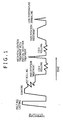
- the production process to be employed herein sequentially includes the steps of melting/casting, soaking, hot rolling, precipitation treatment after hot rolling, cold rolling, recrystallization treatment with partial solution treatment, cold rolling, precipitation treatment, and low-temperature annealing, as schematically illustrated in Fig. 1 .
- Preferred conditions in the respective steps will be described below.
- the soaking is carried out under conditions of holding the work at a temperature of 850°C or higher for a duration of 10 minutes or more, followed by hot rolling.
- the cooling rate from the beginning temperature of hot rolling to 700°C including the hot rolling step is 20°C/minute or more.
- cooling rate to 700°C is lower than the above-specified range, coarse precipitates may be generated, and this may cause insufficiency of precipitates exhibiting pinning effects in the later recrystallization treatment with partial solution treatment and inhibits the precipitation of fine precipitates having hardening or strengthening effects.
- the precipitation treatment after hot rolling is carried out under conditions of holding the work at temperatures of from 300°C to 600°C in the midway of cooling after hot rolling, for a duration of 10 minutes or more.
- the cooling from 700°C to the holding temperature in the precipitation treatment may be carried out at a cooling rate of 20°C/minute or more, subsequent to the cooling from the beginning temperature of the hot rolling to 700°C, but this cooling rate is not essential.
- the precipitation treatment allows dispersed precipitates to precipitate, which will exhibit pinning effects in the later recrystallization treatment. If the holding temperature is lower than 300°C or higher than 600°C, or if the holding duration is less than 10 minutes, the precipitation may be insufficient and the amount of dispersed precipitates exhibiting pining effects is insufficient.
- the cold rolling after the hot rolling is conducted at a reduction ratio of 50% or more, and preferably 80% or more. The cold rolling allows nucleation sites for recrystallization to be introduced.
- the recrystallization treatment with partial solution treatment is carried out under such conditions that the precipitates are not fully dissolved in the Cu matrix (not fully converted into a solution).
- the condition may be selected from conditions of holding the work at temperatures of from 600°C to 950°C, and preferably from 650°C to 900°C, for a duration of 3 minutes or less.
- a suitable temperature of the recrystallization treatment varies depending on the Ni and Si contents in the copper alloy, and the work is preferably held at a lower temperature within the above-specified range at lower Ni and Si contents, and is preferably held at a higher temperature within the above-specified range at higher Ni and Si.contents.
- a temperature which is within the above-specified range and is substantial proportional to the Ni and Si contents maybe selected. Specific preferred temperatures are shown in Examples mentioned later.
- a precipitation/solid-solution reaction in equilibrium with the holding temperature occurs to give certain amounts of precipitates, or precipitates grown during heating are not completely dissolved due to heating for a short time period, and the resulting precipitates exhibit pinning effects during the recrystallization treatment to thereby prevent recrystallized grains from becoming coarse.
- a preferred holding duration becomes shorter with an elevating holding temperature. After the treatment, the work is cooled at a cooling rate of 50°C/second or more.
- the cold rolling after the recrystallization treatment with partial solution treatment is carried out at a reduction ratio of 50% or less.
- the cold rolling if carried out at a high reduction ratio, may impair the bending workability, and it is therefore preferably carried out at a reduction ratio of 50% or less.
- the cold rolling allows nucleation sites for precipitation to be introduced.
- the precipitation treatment is carried out at a temperature of from 350°C to 500°C for a duration of from 30 minutes to 24 hours. These conditions are the same as in common processes.
- a precipitation treatment at a holding temperature lower than 350°C may impede the precipitation of Ni 2 Si.
- a precipitation treatment at a holding temperature higher than 500°C may impair the strength of the copper alloy sheet to thereby fail to ensure necessary yield stress.
- a precipitation treatment for a duration of less than 30 minutes may impede the precipitation of Ni 2 Si, and a precipitation treatment for a duration of more than 24 hours may impair the productivity.
- the low-temperature annealing is carried out according to necessity by holding the work at a temperature of from 300°C to 600°C for a duration of from 1 second to 1 minute, for relieving strain.
- the reduction ratio in cold rolling if conducted after the precipitation treatment, is preferably such that the total reduction ratio with the reduction ratio of the cold rolling carried out prior precipitation treatment be 50% or less.
- dispersed precipitates lying on grain boundaries and having a grain size of from 30 to 300 nm are present in a number of 500 or more per millimeter.
- precipitates precipitated during the precipitation treatment after quenching which is in turn carried out after solution treatment, are fine and generally have a grain size of from several nanometers to thirty (30) nanometers, and most of which have a grain size of less than ten (10) nanometers.
- crystals are coarse, most of which generally have a grain size of more than 300 nm.
- dispersed precipitates having a grain size of 30 to 300 nm and lying on grain boundaries in the copper alloy sheet as a final product are precipitates (Ni 2 Si) which have been produced in the precipitation treatment after hot rolling and which have remained without completely being dissolved during the recrystallization treatment with partial solution treatment, and that these precipitates exhibit pinning effects of grain boundaries to prevent recrystallized grains from becoming coarse during the recrystallization treatment.
- the amount of precipitates having a diameter of 30 to 300 nm is preferably 1000 or more per millimeter.
- the upper limit of the number is not especially limited, but the advantages of the dispersed precipitates may be substantially saturated at a number of 10000 per millimeter.
- Each of copper alloys having compositions in Tables 1 and 2 was melted and cast, while the surface of the melt being covered by charcoal in a cryptol furnace in the atmosphere (air).
- the ingots were heated and soaked by holding at 950°C for 1 hour, followed by hot rolling, the hot rolling was finished at 700°C or higher to give works 20 mm thick.
- Samples Nos. 1 to 30 were held at 500°C for 120 minutes in the midway of cooling and then cooled with water to room temperature.
- the cooling rate of cooling from the beginning temperature of hot rolling to 500°C was 50°C/minute.
- Samples Nos. 31 to 33 were cooled from the beginning temperature of hot rolling to 700°C at a cooling rate of 50°C/minute and then cooled with water from 700°C.
- each of the sheets was subjected to facing each 1 mm on both sides thereof, subjected to cold rolling to a thickness of 0.25 mm (reduction ratio of 98.6%), subjected to a recrystallization treatment with partial solution treatment under conditions in Tables 1 and 2, and subsequently quenched in water.
- Samples Nos. 25 and 27 suffered from cracking during hot rolling, and were not subjected to the cold rolling and subsequent steps.
- Sample No. 25 has excessively high Ni and Si contents
- Sample No. 27 has an excessively high Sn content.
- the other samples were subjected to cold rolling to a thickness of 0.2 mm (reduction ratio of 20%) and then subjected to precipitation treatment at 500°C for 2 hours.
- test pieces were cut from the resulting copper alloy sheets and subjected to measurements of strength (0.2% yield stress) in tensile tests; measurements of electric conductivity; W-bending tests; measurements of crystal grain size; and measurements of dispersed precipitates on grain boundaries, according to the following procedures. The results are shown in Tables 1 and 2.
- JIS Japanese Industrial Standards
- JIS No. 5 test pieces with the rolling direction as a longitudinal direction, to determine a 0.2% yield stress.
- a sample having a yield stress of 500 MPa or more was accepted.
- Electric resistances of test pieces 10 mm wide and 300 mm long with the rolling direction as a longitudinal direction were measured with a double-bridge electrical resistance meter in accordance with the measuring methods for electrical conductivity of non-ferrous materials specified in JIS H-0505, from which electric conductivities were calculated according to the average cross section method.
- W-bending tests at a radium R of 0.05 mm were conducted in accordance with the W-bending test specified by Japan Copper and Brass Association (JCBA) standards T307 on test pieces 10 mm wide and 30 mm long, each having a direction in parallel to the rolling direction (longitudinal to rolling direction, hereinafter abbreviated as "L. D. ”) and a direction transverse to the rolling direction (transverse to rolling direction, hereinafter abbreviated as "T.D.”) as its longitudinal direction.
- L. D. longitudinal to rolling direction
- T.D. transverse to rolling direction
- the crystal grain sizes were measured with a field-emission electron microscope equipped with a back scattered electron diffraction pattern (data collection) system supplied by TSL according to the crystal orientation analytic method. Electron beams were applied at a step of 0.4 ⁇ m to a 125- ⁇ m square region to be measured, and a portion with a difference in crystal orientation of 15 degrees or more was regarded as a grain boundary. The areas of respective crystal grains in the region were measured, and crystal grain sizes (diameters corresponding to circle) were determined.
- the standard deviation ⁇ of crystal grain size was determined from the crystal grain size dn and the occupancy Fn of crystal grain to the total area.
- Thin-film samples were prepared through electropolishing, from which bright-field images were obtained with a field-emission electron microscope at a magnification of 50000 times, and the number of precipitates lying on grain boundaries and having a diameter of from 30 to 300 nm was counted.
- Samples Nos. 1 to 24 have compositions specified in the present invention and satisfy the requirements in the present invention, in which the average size of crystal grains is 10 ⁇ m or less, and the standard deviation ⁇ of crystal grain size satisfies the condition: 2 ⁇ 10 ⁇ m. They also have a number (abundance) of precipitates of 500 or more per millimeter, which lie on grain boundaries and have a diameter of from 30 to 300 nm. Among them, Samples Nos. 1, 2, and 5 to 24 contain a large number of dispersed precipitates, have a small average size of crystal grains of 5 ⁇ m or less, and have a grain size d satisfying the condition: d ⁇ 2 ⁇ . With respect to the properties, SamplesNos. 1 to 24 excel both in strength and W-bending workability (both in L.D. and T.D.).
- Samples Nos. 26, 28, and 29 satisfy the requirements in the present invention regarding the average size of crystal grains, the standard deviation of crystal grain size, and the number (abundance) of dispersed precipitates lying on grainboundaries and having a diameter of from 30 to 300 nm.
- Sample No. 26 is inferior in strength because of low Ni and Si contents; and Samples Nos. 28 and 29 are inferior in bending workability because of excessively high Zn content and excessively high Mg content, respectively.
- Sample No. 30 has an excessively high average size of crystal grains and a small number of dispersed precipitates lying on grain boundaries and is inferior in bending workability. This is probably because the recrystallization treatment was conducted at a high temperature in relation to the Ni and Si contents, precipitates once produced are thereby dissolved to form a solid solution, and this reduces the number (amount) of dispersed precipitates lying on grain boundaries, resulting in the generation of coarse crystal grains in the recrystallization treatment.
- Sample No. 31 has a standard deviation of crystal grain size exceeding the above-specified range and has inferior bending workability. Though satisfying the required conditions of dispersed precipitates in the final product, this sample shows an excessively large standard deviation of crystal grain size as a result of the recrystallization treatment.
- Sample No. 32 has an average size of crystal grains exceeding the above-specified range and a small number of dispersed precipitates lying on grain boundaries and has inferior bending workability. This is probably because dissolution (conversion to solution) proceeds and sufficient dispersed precipitates do not exist due to the absence of precipitation treatment after hot rolling and to the high recrystallization treatment temperature in relation to the Ni and Si contents, and this causes crystal grains to become coarse in the recrystallization treatment.
- Sample No. 33 has an average size of crystal grains and a standard deviation of crystal grain size both exceeding the above-specified ranges and a small number of dispersed precipitates lying on grain boundaries and has inferior bending workability.
Claims (1)
- Feuille en alliage de cuivre ayant d'excellentes résistance et aptitude au formage à utiliser dans des composants électriques et électroniques, la feuille en alliage de cuivre comprenant, de 1,5% à 4,5% en masse de nickel (Ni) et de 0,3% à 1% en masse de silicium (Si), éventuellement soit de 0,01% à 1,3% en masse d'étain (Sn) ou de 0,005% à 0,2% en masse de magnésium (Mg) ou les deux, de 0,01% à 5% en masse de zinc (Zn), soit de 0,01% à 0,5% de manganèse (Mn) ou de 0,001% à 0,3% de chrome (Cr) ou les deux, un total de 0,1% ou moins d'au moins un élément sélectionné parmi le premier groupe d'éléments se composant de B, C, P, S, Ca, V, Ga, Ge, Nb, Mo, Hf, Ta, Bi, et Pb, chacun ayant une teneur allant de 0,0001% à 0,1% ; et un total de 1% ou moins d'au moins un élément sélectionné parmi le deuxième groupe d'éléments se composant de Be, Al, Ti, Fe, Co, Zr, Ag, Cd, In, Sb, Te, et Au, chacun ayant une teneur allant de 0,001% à 1%, la teneur totale des premier et deuxième groupes d'éléments étant de 1% ou moins, le reste étant du cuivre et des impuretés inévitables, où la feuille en alliage de cuivre a une taille moyenne de grain cristallin de 10µm ou moins, une déviation standard σ de la taille du grain cristallin satisfaisant la condition :2σ <10µm, et un nombre de précipités dispersés de 500 ou plus par millimètre, les précipités dispersés se trouvant sur les périphéries des grains et ayant un diamètre allant de 30 à 300 nm.
Applications Claiming Priority (2)
| Application Number | Priority Date | Filing Date | Title |
|---|---|---|---|
| JP2007035726A JP4357536B2 (ja) | 2007-02-16 | 2007-02-16 | 強度と成形性に優れる電気電子部品用銅合金板 |
| PCT/JP2008/052455 WO2008099892A1 (fr) | 2007-02-16 | 2008-02-14 | Feuille d'alliage de cuivre pour pièces électriques et électroniques excellente en termes de résistance mécanique et d'aptitude au formage |
Publications (3)
| Publication Number | Publication Date |
|---|---|
| EP2128282A1 EP2128282A1 (fr) | 2009-12-02 |
| EP2128282A4 EP2128282A4 (fr) | 2011-06-29 |
| EP2128282B1 true EP2128282B1 (fr) | 2012-08-29 |
Family
ID=39690119
Family Applications (1)
| Application Number | Title | Priority Date | Filing Date |
|---|---|---|---|
| EP08711294A Not-in-force EP2128282B1 (fr) | 2007-02-16 | 2008-02-14 | Feuille d'alliage de cuivre pour pièces électriques et électroniques excellente en termes de résistance mécanique et d'aptitude au formage |
Country Status (6)
| Country | Link |
|---|---|
| US (1) | US8784580B2 (fr) |
| EP (1) | EP2128282B1 (fr) |
| JP (1) | JP4357536B2 (fr) |
| KR (2) | KR20120043773A (fr) |
| CN (1) | CN101605917B (fr) |
| WO (1) | WO2008099892A1 (fr) |
Families Citing this family (60)
| Publication number | Priority date | Publication date | Assignee | Title |
|---|---|---|---|---|
| CN1296500C (zh) * | 2003-03-03 | 2007-01-24 | 三宝伸铜工业株式会社 | 耐热铜合金 |
| EP1788585B1 (fr) | 2004-09-10 | 2015-02-18 | Kabushiki Kaisha Kobe Seiko Sho (Kobe Steel, Ltd.) | Matériau conducteur pour pièce de connexion et procédé de fabrication du matériau conducteur |
| JP5170881B2 (ja) * | 2007-03-26 | 2013-03-27 | 古河電気工業株式会社 | 電気・電子機器用銅合金材およびその製造方法 |
| KR101138569B1 (ko) | 2007-12-21 | 2012-05-10 | 미쓰비시 신도 가부시키가이샤 | 고강도?고열전도 동합금관 및 그 제조방법 |
| US9512506B2 (en) * | 2008-02-26 | 2016-12-06 | Mitsubishi Shindoh Co., Ltd. | High strength and high conductivity copper alloy rod or wire |
| JP5051927B2 (ja) * | 2008-03-28 | 2012-10-17 | 三菱伸銅株式会社 | 高強度高導電銅合金管・棒・線材 |
| WO2009123159A1 (fr) * | 2008-03-31 | 2009-10-08 | 古河電気工業株式会社 | Matériau d'alliage de cuivre destiné à des appareils électriques et électroniques, et composants électriques et électroniques |
| WO2009123158A1 (fr) * | 2008-03-31 | 2009-10-08 | 古河電気工業株式会社 | Matériau d'alliage de cuivre destiné à des appareils électriques et électroniques, et composants électriques et électroniques |
| KR101291012B1 (ko) | 2009-01-09 | 2013-07-30 | 미쓰비시 신도 가부시키가이샤 | 고강도 고도전 동합금 압연판 및 그 제조 방법 |
| WO2010079708A1 (fr) | 2009-01-09 | 2010-07-15 | 三菱伸銅株式会社 | Tôle laminée d'alliage de cuivre haute résistance et haute conductivité, et procédé de production correspondant |
| JP2011021225A (ja) * | 2009-07-15 | 2011-02-03 | Hitachi Cable Ltd | 端子・コネクタ用銅合金材及びその製造方法 |
| WO2011068126A1 (fr) * | 2009-12-02 | 2011-06-09 | 古河電気工業株式会社 | Feuille d'alliage de cuivre et son procédé de fabrication |
| US9845521B2 (en) * | 2010-12-13 | 2017-12-19 | Kobe Steel, Ltd. | Copper alloy |
| JP5690169B2 (ja) * | 2011-02-25 | 2015-03-25 | 株式会社神戸製鋼所 | 銅合金 |
| JP2012144789A (ja) * | 2011-01-13 | 2012-08-02 | Jx Nippon Mining & Metals Corp | Cu−Co−Si−Zr合金材 |
| JP5522692B2 (ja) | 2011-02-16 | 2014-06-18 | 株式会社日本製鋼所 | 高強度銅合金鍛造材 |
| KR20140025607A (ko) * | 2011-08-04 | 2014-03-04 | 가부시키가이샤 고베 세이코쇼 | 구리 합금 |
| KR101427060B1 (ko) | 2011-09-16 | 2014-08-05 | 미쓰비시 신도 가부시키가이샤 | 구리합금판 및 구리합금판의 제조방법 |
| WO2013039201A1 (fr) | 2011-09-16 | 2013-03-21 | 三菱伸銅株式会社 | Feuille en un alliage de cuivre et son procédé de production |
| JP6246454B2 (ja) * | 2011-11-02 | 2017-12-13 | Jx金属株式会社 | Cu−Ni−Si系合金及びその製造方法 |
| CN102418004A (zh) * | 2011-11-24 | 2012-04-18 | 中铝洛阳铜业有限公司 | 一种镍铬硅青铜合金材料 |
| JP6029296B2 (ja) * | 2012-03-08 | 2016-11-24 | Jx金属株式会社 | 電気電子機器用Cu−Zn−Sn−Ca合金 |
| JP5773929B2 (ja) * | 2012-03-28 | 2015-09-02 | 株式会社神戸製鋼所 | 曲げ加工性及び耐応力緩和特性に優れる電気電子部品用銅合金板 |
| JP6154996B2 (ja) * | 2012-07-13 | 2017-06-28 | 古河電気工業株式会社 | 高強度銅合金材およびその製造方法 |
| JP6154997B2 (ja) * | 2012-07-13 | 2017-06-28 | 古河電気工業株式会社 | 強度およびめっき性に優れる銅合金材およびその製造方法 |
| JP5988745B2 (ja) * | 2012-07-18 | 2016-09-07 | 三菱伸銅株式会社 | Snめっき付Cu−Ni−Si系銅合金板及びその製造方法 |
| WO2014016934A1 (fr) | 2012-07-26 | 2014-01-30 | 三菱電機株式会社 | Alliage de cuivre et son procédé de production |
| CN102925746B (zh) * | 2012-11-29 | 2014-09-17 | 宁波兴业鑫泰新型电子材料有限公司 | 高性能Cu-Ni-Si系铜合金及其制备和加工方法 |
| CN103146950A (zh) * | 2013-01-11 | 2013-06-12 | 中南大学 | 一种CuNiSi系弹性铜合金及其制备方法 |
| WO2014115307A1 (fr) | 2013-01-25 | 2014-07-31 | 三菱伸銅株式会社 | Plaque en alliage de cuivre pour borne ainsi que matériau de connecteur, et procédé de fabrication de celle-ci |
| DE102013005158A1 (de) * | 2013-03-26 | 2014-10-02 | Kme Germany Gmbh & Co. Kg | Kupferlegierung |
| JP6210887B2 (ja) * | 2014-01-18 | 2017-10-11 | 株式会社神戸製鋼所 | 強度、耐熱性及び曲げ加工性に優れたFe−P系銅合金板 |
| JP6173943B2 (ja) | 2014-02-20 | 2017-08-02 | 株式会社神戸製鋼所 | 耐熱性に優れる表面被覆層付き銅合金板条 |
| KR102113989B1 (ko) * | 2014-08-25 | 2020-05-22 | 가부시키가이샤 고베 세이코쇼 | 내미세접동마모성이 우수한 접속 부품용 도전 재료 |
| CN104152742B (zh) * | 2014-09-04 | 2016-04-20 | 安徽鑫科新材料股份有限公司 | 一种高性能锡磷青铜线及其生产方法 |
| CN104451250A (zh) * | 2014-11-14 | 2015-03-25 | 无锡阳工机械制造有限公司 | 一种耐盐水腐蚀合金的制备方法 |
| CN104480346A (zh) * | 2014-12-25 | 2015-04-01 | 春焱电子科技(苏州)有限公司 | 一种含有钽元素的电子材料用铜合金 |
| CN104630556B (zh) * | 2015-02-06 | 2016-08-17 | 中南大学 | 一种超高强高韧高耐蚀CuNiSiNbSn系弹性铜合金及其制备方法 |
| JP6821290B2 (ja) * | 2015-03-19 | 2021-01-27 | Jx金属株式会社 | 電子部品用Cu−Ni−Co−Si合金 |
| CN104745860A (zh) * | 2015-04-10 | 2015-07-01 | 苏州靖羽新材料有限公司 | 一种电子电气设备用铜合金 |
| CN108076645A (zh) * | 2015-07-17 | 2018-05-25 | 霍尼韦尔国际公司 | 金属和金属合金制品的热处理方法 |
| CN105420534A (zh) * | 2015-11-06 | 2016-03-23 | 广西南宁智翠科技咨询有限公司 | 一种超高导电率的合金导线 |
| CN105349819B (zh) * | 2015-11-26 | 2017-11-28 | 山西春雷铜材有限责任公司 | 一种高强高导铜合金板带的制备方法 |
| KR101627696B1 (ko) * | 2015-12-28 | 2016-06-07 | 주식회사 풍산 | 자동차 및 전기전자 부품용 동합금재 및 그의 제조 방법 |
| CN105695797A (zh) * | 2016-04-20 | 2016-06-22 | 苏州市相城区明达复合材料厂 | 一种铸造加工零部件用青铜合金 |
| CN106191725B (zh) * | 2016-06-24 | 2018-01-26 | 河南江河机械有限责任公司 | 高强度高导电铜合金纳米相析出工艺方法 |
| CN106636736A (zh) * | 2016-12-19 | 2017-05-10 | 昆山哈利法塔金属有限公司 | 一种铜合金材料 |
| DE102017001846A1 (de) | 2017-02-25 | 2018-08-30 | Wieland-Werke Ag | Gleitelement aus einer Kupferlegierung |
| CN107267806A (zh) * | 2017-06-06 | 2017-10-20 | 深圳天珑无线科技有限公司 | 弹片及其制备方法、电子装置 |
| CN107586992A (zh) * | 2017-09-07 | 2018-01-16 | 苏州浩焱精密模具有限公司 | 一种铜合金模具材料及其制备方法 |
| CN108411150B (zh) * | 2018-01-22 | 2019-04-05 | 公牛集团股份有限公司 | 插套用高性能铜合金材料及制造方法 |
| CN108285988B (zh) * | 2018-01-31 | 2019-10-18 | 宁波博威合金材料股份有限公司 | 析出强化型铜合金及其应用 |
| CN110205515B (zh) * | 2019-04-15 | 2020-07-10 | 南阳裕泰隆粉体材料有限公司 | 一种耐腐蚀Cu-Ni合金的制备方法 |
| CN110860855A (zh) * | 2019-10-30 | 2020-03-06 | 富威科技(吴江)有限公司 | 一种高表面短流程铜带生产工艺 |
| CN111636011A (zh) * | 2020-04-26 | 2020-09-08 | 宁夏中色新材料有限公司 | 一种高强度高导电良好成形性的铜镍硅合金及制备方法 |
| KR102210703B1 (ko) * | 2020-06-18 | 2021-02-02 | 주식회사 풍산 | 강도 및 굽힘가공성이 우수한 자동차 또는 전기전자 부품용 동합금판재의 제조 방법 및 이로부터 제조된 동합금판재 |
| CN112877565B (zh) * | 2021-01-12 | 2022-05-20 | 鞍钢股份有限公司 | 一种铜钢固液双金属复合材料及其制备方法 |
| CN113249613B (zh) * | 2021-07-12 | 2021-12-14 | 江西萨瑞微电子技术有限公司 | 一种保护电路用导体引线及包含该引线的保护电路 |
| CN115961173A (zh) * | 2021-10-08 | 2023-04-14 | 刘耀武 | 一种连接器材料、制作工艺及连接器 |
| CN115652136B (zh) * | 2022-10-31 | 2023-12-15 | 宁波金田铜业(集团)股份有限公司 | 一种易切削铜镍硅棒材及其制备方法 |
Family Cites Families (21)
| Publication number | Priority date | Publication date | Assignee | Title |
|---|---|---|---|---|
| JPH03162553A (ja) | 1989-11-22 | 1991-07-12 | Nippon Mining Co Ltd | 曲げ加工性の良好な高強度高導電銅合金の製造方法 |
| JPH03188247A (ja) | 1989-12-14 | 1991-08-16 | Nippon Mining Co Ltd | 曲げ加工性の良好な高強度高導電銅合金の製造方法 |
| JP2597773B2 (ja) | 1991-08-30 | 1997-04-09 | 株式会社神戸製鋼所 | 異方性が少ない高強度銅合金の製造方法 |
| JP3049137B2 (ja) | 1991-12-27 | 2000-06-05 | 株式会社神戸製鋼所 | 曲げ加工性が優れた高力銅合金及びその製造方法 |
| JP3162553B2 (ja) | 1993-09-13 | 2001-05-08 | 本田技研工業株式会社 | 内燃機関の空燃比フィードバック制御装置 |
| JPH10110228A (ja) * | 1996-08-14 | 1998-04-28 | Furukawa Electric Co Ltd:The | 電子機器用銅合金及びその製造方法 |
| JP3739214B2 (ja) | 1998-03-26 | 2006-01-25 | 株式会社神戸製鋼所 | 電子部品用銅合金板 |
| JP2000080428A (ja) | 1998-08-31 | 2000-03-21 | Kobe Steel Ltd | 曲げ加工性が優れた銅合金板 |
| JP3188247B2 (ja) | 1999-04-16 | 2001-07-16 | 株式会社 武田吾慎商店 | 単管フープ足場及びその仮設工法 |
| JP3797882B2 (ja) | 2001-03-09 | 2006-07-19 | 株式会社神戸製鋼所 | 曲げ加工性が優れた銅合金板 |
| US7182823B2 (en) * | 2002-07-05 | 2007-02-27 | Olin Corporation | Copper alloy containing cobalt, nickel and silicon |
| JP4166197B2 (ja) | 2004-06-30 | 2008-10-15 | 日鉱金属株式会社 | BadWayの曲げ加工性が優れたCu−Ni−Si系銅合金条 |
| EP1788585B1 (fr) | 2004-09-10 | 2015-02-18 | Kabushiki Kaisha Kobe Seiko Sho (Kobe Steel, Ltd.) | Matériau conducteur pour pièce de connexion et procédé de fabrication du matériau conducteur |
| JP4566020B2 (ja) | 2005-02-14 | 2010-10-20 | 株式会社神戸製鋼所 | 異方性の小さい電気電子部品用銅合金板 |
| WO2006093140A1 (fr) * | 2005-02-28 | 2006-09-08 | The Furukawa Electric Co., Ltd. | Alliage de cuivre |
| CN101693960B (zh) | 2005-06-08 | 2011-09-07 | 株式会社神户制钢所 | 铜合金、铜合金板及其制造方法 |
| ES2436409T3 (es) | 2006-01-06 | 2013-12-30 | Cordis Corporation | Un sistema de administración médica de una carga médicamente útil |
| KR101049655B1 (ko) | 2006-05-26 | 2011-07-14 | 가부시키가이샤 고베 세이코쇼 | 고강도, 고도전율 및 굽힘 가공성이 뛰어난 구리 합금 |
| JP5025387B2 (ja) | 2007-08-24 | 2012-09-12 | 株式会社神戸製鋼所 | 接続部品用導電材料及びその製造方法 |
| FR3043069B1 (fr) | 2015-10-28 | 2017-12-22 | Georges Sireix | Emballage |
| KR20170080320A (ko) | 2015-12-31 | 2017-07-10 | 엘지디스플레이 주식회사 | 박막트랜지스터, 그를 갖는 표시장치, 및 박막트랜지스터의 제조방법 |
-
2007
- 2007-02-16 JP JP2007035726A patent/JP4357536B2/ja not_active Expired - Fee Related
-
2008
- 2008-02-14 EP EP08711294A patent/EP2128282B1/fr not_active Not-in-force
- 2008-02-14 KR KR1020127008954A patent/KR20120043773A/ko not_active Application Discontinuation
- 2008-02-14 WO PCT/JP2008/052455 patent/WO2008099892A1/fr active Application Filing
- 2008-02-14 CN CN2008800047301A patent/CN101605917B/zh not_active Expired - Fee Related
- 2008-02-14 US US12/523,070 patent/US8784580B2/en not_active Expired - Fee Related
- 2008-02-14 KR KR1020097016823A patent/KR101159404B1/ko active IP Right Grant
Also Published As
| Publication number | Publication date |
|---|---|
| CN101605917B (zh) | 2011-10-05 |
| US8784580B2 (en) | 2014-07-22 |
| KR20090102849A (ko) | 2009-09-30 |
| KR20120043773A (ko) | 2012-05-04 |
| JP2008196042A (ja) | 2008-08-28 |
| JP4357536B2 (ja) | 2009-11-04 |
| US20100047112A1 (en) | 2010-02-25 |
| EP2128282A4 (fr) | 2011-06-29 |
| WO2008099892A1 (fr) | 2008-08-21 |
| EP2128282A1 (fr) | 2009-12-02 |
| KR101159404B1 (ko) | 2012-06-28 |
| CN101605917A (zh) | 2009-12-16 |
Similar Documents
| Publication | Publication Date | Title |
|---|---|---|
| EP2128282B1 (fr) | Feuille d'alliage de cuivre pour pièces électriques et électroniques excellente en termes de résistance mécanique et d'aptitude au formage | |
| EP2371976B1 (fr) | Alliage de cuivre à base de cu-ni-si-co pour des matériaux électroniques et procédé de fabrication de cet alliage | |
| EP1520054B1 (fr) | Alliage de cuivre contenant du cobalt, du nickel et du silicium | |
| EP2778240B1 (fr) | Alliage de cuivre pour dispositifs électroniques, procédé de fabrication d'un alliage de cuivre pour dispositifs électroniques, matériau à déformation plastique en alliage de cuivre pour dispositifs électroniques et composant pour dispositifs électroniques | |
| JP4566020B2 (ja) | 異方性の小さい電気電子部品用銅合金板 | |
| EP3009523B1 (fr) | Alliage de cuivre pour dispositif électronique, procédé de sa production et matière laminée de cet alliage | |
| EP2484787B1 (fr) | Cu-ni-si-co alliage de cuivre pour matériel électronique et son procédé de production | |
| US20130056116A1 (en) | Copper alloy for electronic device, method of producing copper alloy for electronic device, and copper alloy rolled material for electronic device | |
| JP5773929B2 (ja) | 曲げ加工性及び耐応力緩和特性に優れる電気電子部品用銅合金板 | |
| EP2772560B1 (fr) | Alliage de cuivre pour équipement électronique, procédé de production de cet alliage, matériau laminé de cet alliage, et pièce produit de cet alliage | |
| TW201233818A (en) | Copper alloy for electronic and/or electrical device, copper alloy thin plate, and conductive member | |
| EP2940166B1 (fr) | Alliage de cuivre pour équipement électrique et électronique, fine feuille d'alliage de cuivre pour équipement électrique et électronique et partie conductrice et borne pour équipement électrique et électronique | |
| JP2011117034A (ja) | 銅合金材料 | |
| JPWO2010016429A1 (ja) | 電気・電子部品用銅合金材料の製造方法 | |
| EP3020838A1 (fr) | Alliage de cuivre pour équipement électronique et électrique, feuille mince d'alliage de cuivre pour équipement électronique et électrique, et composants conducteurs pour équipement électronique et électrique, terminal | |
| EP2270242B1 (fr) | Matériau d'alliage de cuivre destiné à des appareils électriques ou électroniques, procédé de son fabrication et composant | |
| EP2940167A1 (fr) | Alliage de cuivre pour équipement électrique et électronique, feuille mince d'alliage de cuivre pour équipement électrique et électronique, et partie conductrice et borne pour équipement électrique et électronique | |
| EP2940165A1 (fr) | Alliage de cuivre pour équipement électrique et électronique, fine feuille d'alliage de cuivre pour équipement électrique et électronique et partie conductrice et borne pour équipement électrique et électronique | |
| JP4251672B2 (ja) | 電気電子部品用銅合金 | |
| KR102421870B1 (ko) | 강도, 전기전도도 및 굽힘가공성이 우수한 구리-니켈-실리콘-망간-주석계 동합금재 및 그의 제조 방법 |
Legal Events
| Date | Code | Title | Description |
|---|---|---|---|
| PUAI | Public reference made under article 153(3) epc to a published international application that has entered the european phase |
Free format text: ORIGINAL CODE: 0009012 |
|
| 17P | Request for examination filed |
Effective date: 20090716 |
|
| AK | Designated contracting states |
Kind code of ref document: A1 Designated state(s): AT BE BG CH CY CZ DE DK EE ES FI FR GB GR HR HU IE IS IT LI LT LU LV MC MT NL NO PL PT RO SE SI SK TR |
|
| RIN1 | Information on inventor provided before grant (corrected) |
Inventor name: FUGONO, AKIRA Inventor name: SAKAMOTO, HIROSHI |
|
| DAX | Request for extension of the european patent (deleted) | ||
| A4 | Supplementary search report drawn up and despatched |
Effective date: 20110601 |
|
| RIC1 | Information provided on ipc code assigned before grant |
Ipc: C22F 1/00 20060101ALI20110526BHEP Ipc: C22C 9/06 20060101AFI20080903BHEP Ipc: H01B 1/16 20060101ALI20110526BHEP Ipc: C22F 1/08 20060101ALI20110526BHEP Ipc: C22C 9/04 20060101ALI20110526BHEP |
|
| GRAP | Despatch of communication of intention to grant a patent |
Free format text: ORIGINAL CODE: EPIDOSNIGR1 |
|
| GRAS | Grant fee paid |
Free format text: ORIGINAL CODE: EPIDOSNIGR3 |
|
| GRAA | (expected) grant |
Free format text: ORIGINAL CODE: 0009210 |
|
| AK | Designated contracting states |
Kind code of ref document: B1 Designated state(s): AT BE BG CH CY CZ DE DK EE ES FI FR GB GR HR HU IE IS IT LI LT LU LV MC MT NL NO PL PT RO SE SI SK TR |
|
| REG | Reference to a national code |
Ref country code: GB Ref legal event code: FG4D |
|
| REG | Reference to a national code |
Ref country code: CH Ref legal event code: EP |
|
| REG | Reference to a national code |
Ref country code: AT Ref legal event code: REF Ref document number: 573149 Country of ref document: AT Kind code of ref document: T Effective date: 20120915 |
|
| REG | Reference to a national code |
Ref country code: IE Ref legal event code: FG4D |
|
| REG | Reference to a national code |
Ref country code: DE Ref legal event code: R096 Ref document number: 602008018358 Country of ref document: DE Effective date: 20121025 |
|
| REG | Reference to a national code |
Ref country code: AT Ref legal event code: MK05 Ref document number: 573149 Country of ref document: AT Kind code of ref document: T Effective date: 20120829 |
|
| REG | Reference to a national code |
Ref country code: NL Ref legal event code: VDEP Effective date: 20120829 |
|
| REG | Reference to a national code |
Ref country code: LT Ref legal event code: MG4D Effective date: 20120829 |
|
| PG25 | Lapsed in a contracting state [announced via postgrant information from national office to epo] |
Ref country code: AT Free format text: LAPSE BECAUSE OF FAILURE TO SUBMIT A TRANSLATION OF THE DESCRIPTION OR TO PAY THE FEE WITHIN THE PRESCRIBED TIME-LIMIT Effective date: 20120829 Ref country code: LT Free format text: LAPSE BECAUSE OF FAILURE TO SUBMIT A TRANSLATION OF THE DESCRIPTION OR TO PAY THE FEE WITHIN THE PRESCRIBED TIME-LIMIT Effective date: 20120829 Ref country code: FI Free format text: LAPSE BECAUSE OF FAILURE TO SUBMIT A TRANSLATION OF THE DESCRIPTION OR TO PAY THE FEE WITHIN THE PRESCRIBED TIME-LIMIT Effective date: 20120829 Ref country code: CY Free format text: LAPSE BECAUSE OF FAILURE TO SUBMIT A TRANSLATION OF THE DESCRIPTION OR TO PAY THE FEE WITHIN THE PRESCRIBED TIME-LIMIT Effective date: 20120829 Ref country code: HR Free format text: LAPSE BECAUSE OF FAILURE TO SUBMIT A TRANSLATION OF THE DESCRIPTION OR TO PAY THE FEE WITHIN THE PRESCRIBED TIME-LIMIT Effective date: 20120829 Ref country code: IS Free format text: LAPSE BECAUSE OF FAILURE TO SUBMIT A TRANSLATION OF THE DESCRIPTION OR TO PAY THE FEE WITHIN THE PRESCRIBED TIME-LIMIT Effective date: 20121229 Ref country code: NO Free format text: LAPSE BECAUSE OF FAILURE TO SUBMIT A TRANSLATION OF THE DESCRIPTION OR TO PAY THE FEE WITHIN THE PRESCRIBED TIME-LIMIT Effective date: 20121129 |
|
| PG25 | Lapsed in a contracting state [announced via postgrant information from national office to epo] |
Ref country code: SE Free format text: LAPSE BECAUSE OF FAILURE TO SUBMIT A TRANSLATION OF THE DESCRIPTION OR TO PAY THE FEE WITHIN THE PRESCRIBED TIME-LIMIT Effective date: 20120829 Ref country code: SI Free format text: LAPSE BECAUSE OF FAILURE TO SUBMIT A TRANSLATION OF THE DESCRIPTION OR TO PAY THE FEE WITHIN THE PRESCRIBED TIME-LIMIT Effective date: 20120829 Ref country code: PT Free format text: LAPSE BECAUSE OF FAILURE TO SUBMIT A TRANSLATION OF THE DESCRIPTION OR TO PAY THE FEE WITHIN THE PRESCRIBED TIME-LIMIT Effective date: 20121231 Ref country code: BE Free format text: LAPSE BECAUSE OF FAILURE TO SUBMIT A TRANSLATION OF THE DESCRIPTION OR TO PAY THE FEE WITHIN THE PRESCRIBED TIME-LIMIT Effective date: 20120829 Ref country code: GR Free format text: LAPSE BECAUSE OF FAILURE TO SUBMIT A TRANSLATION OF THE DESCRIPTION OR TO PAY THE FEE WITHIN THE PRESCRIBED TIME-LIMIT Effective date: 20121130 Ref country code: LV Free format text: LAPSE BECAUSE OF FAILURE TO SUBMIT A TRANSLATION OF THE DESCRIPTION OR TO PAY THE FEE WITHIN THE PRESCRIBED TIME-LIMIT Effective date: 20120829 |
|
| PG25 | Lapsed in a contracting state [announced via postgrant information from national office to epo] |
Ref country code: EE Free format text: LAPSE BECAUSE OF FAILURE TO SUBMIT A TRANSLATION OF THE DESCRIPTION OR TO PAY THE FEE WITHIN THE PRESCRIBED TIME-LIMIT Effective date: 20120829 Ref country code: CZ Free format text: LAPSE BECAUSE OF FAILURE TO SUBMIT A TRANSLATION OF THE DESCRIPTION OR TO PAY THE FEE WITHIN THE PRESCRIBED TIME-LIMIT Effective date: 20120829 Ref country code: RO Free format text: LAPSE BECAUSE OF FAILURE TO SUBMIT A TRANSLATION OF THE DESCRIPTION OR TO PAY THE FEE WITHIN THE PRESCRIBED TIME-LIMIT Effective date: 20120829 Ref country code: NL Free format text: LAPSE BECAUSE OF FAILURE TO SUBMIT A TRANSLATION OF THE DESCRIPTION OR TO PAY THE FEE WITHIN THE PRESCRIBED TIME-LIMIT Effective date: 20120829 Ref country code: ES Free format text: LAPSE BECAUSE OF FAILURE TO SUBMIT A TRANSLATION OF THE DESCRIPTION OR TO PAY THE FEE WITHIN THE PRESCRIBED TIME-LIMIT Effective date: 20121210 Ref country code: DK Free format text: LAPSE BECAUSE OF FAILURE TO SUBMIT A TRANSLATION OF THE DESCRIPTION OR TO PAY THE FEE WITHIN THE PRESCRIBED TIME-LIMIT Effective date: 20120829 |
|
| PG25 | Lapsed in a contracting state [announced via postgrant information from national office to epo] |
Ref country code: IT Free format text: LAPSE BECAUSE OF FAILURE TO SUBMIT A TRANSLATION OF THE DESCRIPTION OR TO PAY THE FEE WITHIN THE PRESCRIBED TIME-LIMIT Effective date: 20120829 Ref country code: PL Free format text: LAPSE BECAUSE OF FAILURE TO SUBMIT A TRANSLATION OF THE DESCRIPTION OR TO PAY THE FEE WITHIN THE PRESCRIBED TIME-LIMIT Effective date: 20120829 Ref country code: SK Free format text: LAPSE BECAUSE OF FAILURE TO SUBMIT A TRANSLATION OF THE DESCRIPTION OR TO PAY THE FEE WITHIN THE PRESCRIBED TIME-LIMIT Effective date: 20120829 |
|
| PLBE | No opposition filed within time limit |
Free format text: ORIGINAL CODE: 0009261 |
|
| STAA | Information on the status of an ep patent application or granted ep patent |
Free format text: STATUS: NO OPPOSITION FILED WITHIN TIME LIMIT |
|
| PG25 | Lapsed in a contracting state [announced via postgrant information from national office to epo] |
Ref country code: BG Free format text: LAPSE BECAUSE OF FAILURE TO SUBMIT A TRANSLATION OF THE DESCRIPTION OR TO PAY THE FEE WITHIN THE PRESCRIBED TIME-LIMIT Effective date: 20121129 |
|
| 26N | No opposition filed |
Effective date: 20130530 |
|
| REG | Reference to a national code |
Ref country code: DE Ref legal event code: R097 Ref document number: 602008018358 Country of ref document: DE Effective date: 20130530 |
|
| PG25 | Lapsed in a contracting state [announced via postgrant information from national office to epo] |
Ref country code: MC Free format text: LAPSE BECAUSE OF NON-PAYMENT OF DUE FEES Effective date: 20130228 |
|
| REG | Reference to a national code |
Ref country code: CH Ref legal event code: PL |
|
| GBPC | Gb: european patent ceased through non-payment of renewal fee |
Effective date: 20130214 |
|
| PG25 | Lapsed in a contracting state [announced via postgrant information from national office to epo] |
Ref country code: CH Free format text: LAPSE BECAUSE OF NON-PAYMENT OF DUE FEES Effective date: 20130228 Ref country code: LI Free format text: LAPSE BECAUSE OF NON-PAYMENT OF DUE FEES Effective date: 20130228 |
|
| REG | Reference to a national code |
Ref country code: FR Ref legal event code: ST Effective date: 20131031 |
|
| REG | Reference to a national code |
Ref country code: IE Ref legal event code: MM4A |
|
| PG25 | Lapsed in a contracting state [announced via postgrant information from national office to epo] |
Ref country code: IE Free format text: LAPSE BECAUSE OF NON-PAYMENT OF DUE FEES Effective date: 20130214 Ref country code: FR Free format text: LAPSE BECAUSE OF NON-PAYMENT OF DUE FEES Effective date: 20130228 Ref country code: GB Free format text: LAPSE BECAUSE OF NON-PAYMENT OF DUE FEES Effective date: 20130214 |
|
| PG25 | Lapsed in a contracting state [announced via postgrant information from national office to epo] |
Ref country code: MT Free format text: LAPSE BECAUSE OF FAILURE TO SUBMIT A TRANSLATION OF THE DESCRIPTION OR TO PAY THE FEE WITHIN THE PRESCRIBED TIME-LIMIT Effective date: 20120829 |
|
| PG25 | Lapsed in a contracting state [announced via postgrant information from national office to epo] |
Ref country code: TR Free format text: LAPSE BECAUSE OF FAILURE TO SUBMIT A TRANSLATION OF THE DESCRIPTION OR TO PAY THE FEE WITHIN THE PRESCRIBED TIME-LIMIT Effective date: 20120829 |
|
| PG25 | Lapsed in a contracting state [announced via postgrant information from national office to epo] |
Ref country code: LU Free format text: LAPSE BECAUSE OF NON-PAYMENT OF DUE FEES Effective date: 20130214 Ref country code: HU Free format text: LAPSE BECAUSE OF FAILURE TO SUBMIT A TRANSLATION OF THE DESCRIPTION OR TO PAY THE FEE WITHIN THE PRESCRIBED TIME-LIMIT; INVALID AB INITIO Effective date: 20080214 |
|
| PGFP | Annual fee paid to national office [announced via postgrant information from national office to epo] |
Ref country code: DE Payment date: 20210202 Year of fee payment: 14 |
|
| REG | Reference to a national code |
Ref country code: DE Ref legal event code: R119 Ref document number: 602008018358 Country of ref document: DE |
|
| PG25 | Lapsed in a contracting state [announced via postgrant information from national office to epo] |
Ref country code: DE Free format text: LAPSE BECAUSE OF NON-PAYMENT OF DUE FEES Effective date: 20220901 |