EP2078978A2 - LCD rétroéclairage comprenant un LED avec émission de lumière adaptée et des filtres de couleur convenables - Google Patents
LCD rétroéclairage comprenant un LED avec émission de lumière adaptée et des filtres de couleur convenables Download PDFInfo
- Publication number
- EP2078978A2 EP2078978A2 EP20090004404 EP09004404A EP2078978A2 EP 2078978 A2 EP2078978 A2 EP 2078978A2 EP 20090004404 EP20090004404 EP 20090004404 EP 09004404 A EP09004404 A EP 09004404A EP 2078978 A2 EP2078978 A2 EP 2078978A2
- Authority
- EP
- European Patent Office
- Prior art keywords
- backlight
- phosphor
- color
- light
- color filter
- Prior art date
- Legal status (The legal status is an assumption and is not a legal conclusion. Google has not performed a legal analysis and makes no representation as to the accuracy of the status listed.)
- Withdrawn
Links
- OAICVXFJPJFONN-UHFFFAOYSA-N Phosphorus Chemical compound [P] OAICVXFJPJFONN-UHFFFAOYSA-N 0.000 claims abstract description 124
- 239000003086 colorant Substances 0.000 claims abstract description 51
- 238000002834 transmittance Methods 0.000 claims abstract description 32
- 230000005540 biological transmission Effects 0.000 claims abstract description 20
- 238000005286 illumination Methods 0.000 claims abstract description 16
- 230000003595 spectral effect Effects 0.000 claims abstract description 14
- 229910052751 metal Inorganic materials 0.000 claims description 50
- 150000001875 compounds Chemical class 0.000 claims description 45
- 239000002184 metal Substances 0.000 claims description 32
- 229910052693 Europium Inorganic materials 0.000 claims description 17
- 239000012190 activator Substances 0.000 claims description 17
- 239000000463 material Substances 0.000 claims description 14
- 229910052684 Cerium Inorganic materials 0.000 claims description 11
- 229910052769 Ytterbium Inorganic materials 0.000 claims description 10
- 229910052749 magnesium Inorganic materials 0.000 claims description 10
- OGPBJKLSAFTDLK-UHFFFAOYSA-N europium atom Chemical compound [Eu] OGPBJKLSAFTDLK-UHFFFAOYSA-N 0.000 claims description 9
- 229910052692 Dysprosium Inorganic materials 0.000 claims description 8
- 229910052772 Samarium Inorganic materials 0.000 claims description 8
- 229910052771 Terbium Inorganic materials 0.000 claims description 8
- 229910052788 barium Inorganic materials 0.000 claims description 8
- 229910052748 manganese Inorganic materials 0.000 claims description 8
- 229910052725 zinc Inorganic materials 0.000 claims description 8
- 229910052691 Erbium Inorganic materials 0.000 claims description 7
- 229910052757 nitrogen Inorganic materials 0.000 claims description 7
- 229910052689 Holmium Inorganic materials 0.000 claims description 6
- 229910052779 Neodymium Inorganic materials 0.000 claims description 6
- 229910052777 Praseodymium Inorganic materials 0.000 claims description 6
- 229910052775 Thulium Inorganic materials 0.000 claims description 6
- 229910052760 oxygen Inorganic materials 0.000 claims description 6
- 229910052731 fluorine Inorganic materials 0.000 claims description 5
- ZMIGMASIKSOYAM-UHFFFAOYSA-N cerium Chemical compound [Ce][Ce][Ce][Ce][Ce][Ce][Ce][Ce][Ce][Ce][Ce][Ce][Ce][Ce][Ce][Ce][Ce][Ce][Ce][Ce][Ce][Ce][Ce][Ce][Ce][Ce][Ce][Ce][Ce][Ce][Ce][Ce][Ce][Ce][Ce][Ce][Ce][Ce] ZMIGMASIKSOYAM-UHFFFAOYSA-N 0.000 claims description 4
- 239000000203 mixture Substances 0.000 description 78
- 239000000049 pigment Substances 0.000 description 67
- 238000002360 preparation method Methods 0.000 description 48
- 229920005989 resin Polymers 0.000 description 48
- 239000011347 resin Substances 0.000 description 48
- 238000000034 method Methods 0.000 description 46
- 239000006185 dispersion Substances 0.000 description 36
- 239000000758 substrate Substances 0.000 description 31
- 239000010408 film Substances 0.000 description 30
- 239000000975 dye Substances 0.000 description 28
- 150000002148 esters Chemical class 0.000 description 28
- 239000011230 binding agent Substances 0.000 description 25
- 239000004973 liquid crystal related substance Substances 0.000 description 25
- NIXOWILDQLNWCW-UHFFFAOYSA-M Acrylate Chemical compound [O-]C(=O)C=C NIXOWILDQLNWCW-UHFFFAOYSA-M 0.000 description 24
- 238000011161 development Methods 0.000 description 23
- -1 polyethylene terephthalate Polymers 0.000 description 23
- 239000000178 monomer Substances 0.000 description 20
- XNGIFLGASWRNHJ-UHFFFAOYSA-N phthalic acid Chemical compound OC(=O)C1=CC=CC=C1C(O)=O XNGIFLGASWRNHJ-UHFFFAOYSA-N 0.000 description 20
- 239000000126 substance Substances 0.000 description 18
- 239000011248 coating agent Substances 0.000 description 17
- 238000000576 coating method Methods 0.000 description 17
- 239000013078 crystal Substances 0.000 description 16
- 239000000976 ink Substances 0.000 description 16
- 239000010410 layer Substances 0.000 description 16
- KDYFGRWQOYBRFD-UHFFFAOYSA-N Succinic acid Natural products OC(=O)CCC(O)=O KDYFGRWQOYBRFD-UHFFFAOYSA-N 0.000 description 15
- 230000007423 decrease Effects 0.000 description 15
- 238000000295 emission spectrum Methods 0.000 description 15
- 239000011521 glass Substances 0.000 description 15
- 239000007787 solid Substances 0.000 description 15
- 239000002904 solvent Substances 0.000 description 15
- VZCYOOQTPOCHFL-UHFFFAOYSA-N trans-butenedioic acid Natural products OC(=O)C=CC(O)=O VZCYOOQTPOCHFL-UHFFFAOYSA-N 0.000 description 14
- 230000003247 decreasing effect Effects 0.000 description 13
- VZCYOOQTPOCHFL-UPHRSURJSA-N maleic acid Chemical compound OC(=O)\C=C/C(O)=O VZCYOOQTPOCHFL-UPHRSURJSA-N 0.000 description 13
- 238000004519 manufacturing process Methods 0.000 description 12
- CERQOIWHTDAKMF-UHFFFAOYSA-N Methacrylic acid Chemical compound CC(=C)C(O)=O CERQOIWHTDAKMF-UHFFFAOYSA-N 0.000 description 11
- OFOBLEOULBTSOW-UHFFFAOYSA-N Propanedioic acid Natural products OC(=O)CC(O)=O OFOBLEOULBTSOW-UHFFFAOYSA-N 0.000 description 11
- 150000001732 carboxylic acid derivatives Chemical class 0.000 description 11
- 239000011976 maleic acid Substances 0.000 description 11
- 239000011159 matrix material Substances 0.000 description 11
- WNLRTRBMVRJNCN-UHFFFAOYSA-N adipic acid Chemical compound OC(=O)CCCCC(O)=O WNLRTRBMVRJNCN-UHFFFAOYSA-N 0.000 description 10
- 230000008859 change Effects 0.000 description 10
- 238000001035 drying Methods 0.000 description 10
- 239000000243 solution Substances 0.000 description 10
- CGLVZFOCZLHKOH-UHFFFAOYSA-N 8,18-dichloro-5,15-diethyl-5,15-dihydrodiindolo(3,2-b:3',2'-m)triphenodioxazine Chemical compound CCN1C2=CC=CC=C2C2=C1C=C1OC3=C(Cl)C4=NC(C=C5C6=CC=CC=C6N(C5=C5)CC)=C5OC4=C(Cl)C3=NC1=C2 CGLVZFOCZLHKOH-UHFFFAOYSA-N 0.000 description 9
- 239000002253 acid Substances 0.000 description 9
- 238000013329 compounding Methods 0.000 description 9
- 230000000977 initiatory effect Effects 0.000 description 9
- 230000008569 process Effects 0.000 description 9
- KWYUFKZDYYNOTN-UHFFFAOYSA-M Potassium hydroxide Chemical compound [OH-].[K+] KWYUFKZDYYNOTN-UHFFFAOYSA-M 0.000 description 8
- PPBRXRYQALVLMV-UHFFFAOYSA-N Styrene Chemical compound C=CC1=CC=CC=C1 PPBRXRYQALVLMV-UHFFFAOYSA-N 0.000 description 8
- 239000000654 additive Substances 0.000 description 8
- 229910052782 aluminium Inorganic materials 0.000 description 8
- 239000002585 base Substances 0.000 description 8
- 229910052706 scandium Inorganic materials 0.000 description 8
- MCSXGCZMEPXKIW-UHFFFAOYSA-N 3-hydroxy-4-[(4-methyl-2-nitrophenyl)diazenyl]-N-(3-nitrophenyl)naphthalene-2-carboxamide Chemical compound Cc1ccc(N=Nc2c(O)c(cc3ccccc23)C(=O)Nc2cccc(c2)[N+]([O-])=O)c(c1)[N+]([O-])=O MCSXGCZMEPXKIW-UHFFFAOYSA-N 0.000 description 7
- 229910052765 Lutetium Inorganic materials 0.000 description 7
- NIXOWILDQLNWCW-UHFFFAOYSA-N acrylic acid group Chemical group C(C=C)(=O)O NIXOWILDQLNWCW-UHFFFAOYSA-N 0.000 description 7
- 125000003178 carboxy group Chemical group [H]OC(*)=O 0.000 description 7
- RBTKNAXYKSUFRK-UHFFFAOYSA-N heliogen blue Chemical compound [Cu].[N-]1C2=C(C=CC=C3)C3=C1N=C([N-]1)C3=CC=CC=C3C1=NC([N-]1)=C(C=CC=C3)C3=C1N=C([N-]1)C3=CC=CC=C3C1=N2 RBTKNAXYKSUFRK-UHFFFAOYSA-N 0.000 description 7
- 230000014759 maintenance of location Effects 0.000 description 7
- 239000000047 product Substances 0.000 description 7
- LLHKCFNBLRBOGN-UHFFFAOYSA-N propylene glycol methyl ether acetate Chemical compound COCC(C)OC(C)=O LLHKCFNBLRBOGN-UHFFFAOYSA-N 0.000 description 7
- 239000010409 thin film Substances 0.000 description 7
- 239000004925 Acrylic resin Substances 0.000 description 6
- 229920000178 Acrylic resin Polymers 0.000 description 6
- DNIAPMSPPWPWGF-UHFFFAOYSA-N Propylene glycol Chemical compound CC(O)CO DNIAPMSPPWPWGF-UHFFFAOYSA-N 0.000 description 6
- MCMNRKCIXSYSNV-UHFFFAOYSA-N Zirconium dioxide Chemical compound O=[Zr]=O MCMNRKCIXSYSNV-UHFFFAOYSA-N 0.000 description 6
- 239000003513 alkali Substances 0.000 description 6
- 239000003795 chemical substances by application Substances 0.000 description 6
- 230000001965 increasing effect Effects 0.000 description 6
- 230000035945 sensitivity Effects 0.000 description 6
- 230000001235 sensitizing effect Effects 0.000 description 6
- 229910052712 strontium Inorganic materials 0.000 description 6
- 239000000853 adhesive Substances 0.000 description 5
- 230000001070 adhesive effect Effects 0.000 description 5
- 239000001361 adipic acid Substances 0.000 description 5
- 235000011037 adipic acid Nutrition 0.000 description 5
- 239000011324 bead Substances 0.000 description 5
- KDYFGRWQOYBRFD-NUQCWPJISA-N butanedioic acid Chemical compound O[14C](=O)CC[14C](O)=O KDYFGRWQOYBRFD-NUQCWPJISA-N 0.000 description 5
- 229910052791 calcium Inorganic materials 0.000 description 5
- 229910052804 chromium Inorganic materials 0.000 description 5
- 239000011651 chromium Substances 0.000 description 5
- QSAWQNUELGIYBC-UHFFFAOYSA-N cyclohexane-1,2-dicarboxylic acid Chemical compound OC(=O)C1CCCCC1C(O)=O QSAWQNUELGIYBC-UHFFFAOYSA-N 0.000 description 5
- 230000000694 effects Effects 0.000 description 5
- 239000001056 green pigment Substances 0.000 description 5
- 150000002440 hydroxy compounds Chemical class 0.000 description 5
- 125000002887 hydroxy group Chemical group [H]O* 0.000 description 5
- 150000002500 ions Chemical class 0.000 description 5
- QSHDDOUJBYECFT-UHFFFAOYSA-N mercury Chemical compound [Hg] QSHDDOUJBYECFT-UHFFFAOYSA-N 0.000 description 5
- 229910052753 mercury Inorganic materials 0.000 description 5
- 238000002156 mixing Methods 0.000 description 5
- PXHVJJICTQNCMI-UHFFFAOYSA-N nickel Substances [Ni] PXHVJJICTQNCMI-UHFFFAOYSA-N 0.000 description 5
- 239000002245 particle Substances 0.000 description 5
- 239000001384 succinic acid Substances 0.000 description 5
- 238000012719 thermal polymerization Methods 0.000 description 5
- 239000001052 yellow pigment Substances 0.000 description 5
- YXIWHUQXZSMYRE-UHFFFAOYSA-N 1,3-benzothiazole-2-thiol Chemical compound C1=CC=C2SC(S)=NC2=C1 YXIWHUQXZSMYRE-UHFFFAOYSA-N 0.000 description 4
- SMZOUWXMTYCWNB-UHFFFAOYSA-N 2-(2-methoxy-5-methylphenyl)ethanamine Chemical compound COC1=CC=C(C)C=C1CCN SMZOUWXMTYCWNB-UHFFFAOYSA-N 0.000 description 4
- YEJRWHAVMIAJKC-UHFFFAOYSA-N 4-Butyrolactone Chemical compound O=C1CCCO1 YEJRWHAVMIAJKC-UHFFFAOYSA-N 0.000 description 4
- OZJPLYNZGCXSJM-UHFFFAOYSA-N 5-valerolactone Chemical compound O=C1CCCCO1 OZJPLYNZGCXSJM-UHFFFAOYSA-N 0.000 description 4
- IJGRMHOSHXDMSA-UHFFFAOYSA-N Atomic nitrogen Chemical compound N#N IJGRMHOSHXDMSA-UHFFFAOYSA-N 0.000 description 4
- JOYRKODLDBILNP-UHFFFAOYSA-N Ethyl urethane Chemical compound CCOC(N)=O JOYRKODLDBILNP-UHFFFAOYSA-N 0.000 description 4
- VZCYOOQTPOCHFL-OWOJBTEDSA-N Fumaric acid Chemical compound OC(=O)\C=C\C(O)=O VZCYOOQTPOCHFL-OWOJBTEDSA-N 0.000 description 4
- 229920003171 Poly (ethylene oxide) Polymers 0.000 description 4
- SMWDFEZZVXVKRB-UHFFFAOYSA-N Quinoline Chemical compound N1=CC=CC2=CC=CC=C21 SMWDFEZZVXVKRB-UHFFFAOYSA-N 0.000 description 4
- 150000001252 acrylic acid derivatives Chemical class 0.000 description 4
- 125000003647 acryloyl group Chemical group O=C([*])C([H])=C([H])[H] 0.000 description 4
- 125000001931 aliphatic group Chemical group 0.000 description 4
- 150000001450 anions Chemical class 0.000 description 4
- 238000006243 chemical reaction Methods 0.000 description 4
- 239000007859 condensation product Substances 0.000 description 4
- 229920001577 copolymer Polymers 0.000 description 4
- LDHQCZJRKDOVOX-NSCUHMNNSA-N crotonic acid Chemical compound C\C=C\C(O)=O LDHQCZJRKDOVOX-NSCUHMNNSA-N 0.000 description 4
- 230000005611 electricity Effects 0.000 description 4
- 239000003822 epoxy resin Substances 0.000 description 4
- 125000004464 hydroxyphenyl group Chemical group 0.000 description 4
- 230000006872 improvement Effects 0.000 description 4
- 239000003112 inhibitor Substances 0.000 description 4
- LVHBHZANLOWSRM-UHFFFAOYSA-N methylenebutanedioic acid Natural products OC(=O)CC(=C)C(O)=O LVHBHZANLOWSRM-UHFFFAOYSA-N 0.000 description 4
- 229910052759 nickel Inorganic materials 0.000 description 4
- 239000003960 organic solvent Substances 0.000 description 4
- 238000000016 photochemical curing Methods 0.000 description 4
- IEQIEDJGQAUEQZ-UHFFFAOYSA-N phthalocyanine Chemical compound N1C(N=C2C3=CC=CC=C3C(N=C3C4=CC=CC=C4C(=N4)N3)=N2)=C(C=CC=C2)C2=C1N=C1C2=CC=CC=C2C4=N1 IEQIEDJGQAUEQZ-UHFFFAOYSA-N 0.000 description 4
- 239000004014 plasticizer Substances 0.000 description 4
- 229920000647 polyepoxide Polymers 0.000 description 4
- 238000007639 printing Methods 0.000 description 4
- WQGWDDDVZFFDIG-UHFFFAOYSA-N pyrogallol Chemical compound OC1=CC=CC(O)=C1O WQGWDDDVZFFDIG-UHFFFAOYSA-N 0.000 description 4
- 239000004094 surface-active agent Substances 0.000 description 4
- 229910052727 yttrium Inorganic materials 0.000 description 4
- ZWEHNKRNPOVVGH-UHFFFAOYSA-N 2-Butanone Chemical compound CCC(C)=O ZWEHNKRNPOVVGH-UHFFFAOYSA-N 0.000 description 3
- HRPVXLWXLXDGHG-UHFFFAOYSA-N Acrylamide Chemical compound NC(=O)C=C HRPVXLWXLXDGHG-UHFFFAOYSA-N 0.000 description 3
- OKTJSMMVPCPJKN-UHFFFAOYSA-N Carbon Chemical compound [C] OKTJSMMVPCPJKN-UHFFFAOYSA-N 0.000 description 3
- VYZAMTAEIAYCRO-UHFFFAOYSA-N Chromium Chemical compound [Cr] VYZAMTAEIAYCRO-UHFFFAOYSA-N 0.000 description 3
- RTZKZFJDLAIYFH-UHFFFAOYSA-N Diethyl ether Chemical compound CCOCC RTZKZFJDLAIYFH-UHFFFAOYSA-N 0.000 description 3
- 239000004593 Epoxy Substances 0.000 description 3
- XEKOWRVHYACXOJ-UHFFFAOYSA-N Ethyl acetate Chemical compound CCOC(C)=O XEKOWRVHYACXOJ-UHFFFAOYSA-N 0.000 description 3
- LYCAIKOWRPUZTN-UHFFFAOYSA-N Ethylene glycol Chemical compound OCCO LYCAIKOWRPUZTN-UHFFFAOYSA-N 0.000 description 3
- 229910052688 Gadolinium Inorganic materials 0.000 description 3
- PEDCQBHIVMGVHV-UHFFFAOYSA-N Glycerine Chemical compound OCC(O)CO PEDCQBHIVMGVHV-UHFFFAOYSA-N 0.000 description 3
- KFZMGEQAYNKOFK-UHFFFAOYSA-N Isopropanol Chemical compound CC(C)O KFZMGEQAYNKOFK-UHFFFAOYSA-N 0.000 description 3
- WMFOQBRAJBCJND-UHFFFAOYSA-M Lithium hydroxide Chemical compound [Li+].[OH-] WMFOQBRAJBCJND-UHFFFAOYSA-M 0.000 description 3
- BQCADISMDOOEFD-UHFFFAOYSA-N Silver Chemical compound [Ag] BQCADISMDOOEFD-UHFFFAOYSA-N 0.000 description 3
- HEMHJVSKTPXQMS-UHFFFAOYSA-M Sodium hydroxide Chemical compound [OH-].[Na+] HEMHJVSKTPXQMS-UHFFFAOYSA-M 0.000 description 3
- GWEVSGVZZGPLCZ-UHFFFAOYSA-N Titan oxide Chemical compound O=[Ti]=O GWEVSGVZZGPLCZ-UHFFFAOYSA-N 0.000 description 3
- WGLPBDUCMAPZCE-UHFFFAOYSA-N Trioxochromium Chemical compound O=[Cr](=O)=O WGLPBDUCMAPZCE-UHFFFAOYSA-N 0.000 description 3
- 230000000996 additive effect Effects 0.000 description 3
- 239000007864 aqueous solution Substances 0.000 description 3
- 125000003118 aryl group Chemical group 0.000 description 3
- JFDZBHWFFUWGJE-UHFFFAOYSA-N benzonitrile Chemical compound N#CC1=CC=CC=C1 JFDZBHWFFUWGJE-UHFFFAOYSA-N 0.000 description 3
- 229910000423 chromium oxide Inorganic materials 0.000 description 3
- 229910052802 copper Inorganic materials 0.000 description 3
- 239000010949 copper Substances 0.000 description 3
- MTHSVFCYNBDYFN-UHFFFAOYSA-N diethylene glycol Chemical compound OCCOCCO MTHSVFCYNBDYFN-UHFFFAOYSA-N 0.000 description 3
- PPSZHCXTGRHULJ-UHFFFAOYSA-N dioxazine Chemical compound O1ON=CC=C1 PPSZHCXTGRHULJ-UHFFFAOYSA-N 0.000 description 3
- 239000002270 dispersing agent Substances 0.000 description 3
- 238000009826 distribution Methods 0.000 description 3
- 238000004043 dyeing Methods 0.000 description 3
- 238000004070 electrodeposition Methods 0.000 description 3
- 238000005530 etching Methods 0.000 description 3
- 229910052735 hafnium Inorganic materials 0.000 description 3
- 235000019239 indanthrene blue RS Nutrition 0.000 description 3
- UHOKSCJSTAHBSO-UHFFFAOYSA-N indanthrone blue Chemical compound C1=CC=C2C(=O)C3=CC=C4NC5=C6C(=O)C7=CC=CC=C7C(=O)C6=CC=C5NC4=C3C(=O)C2=C1 UHOKSCJSTAHBSO-UHFFFAOYSA-N 0.000 description 3
- 229910052738 indium Inorganic materials 0.000 description 3
- 239000001023 inorganic pigment Substances 0.000 description 3
- 229910052742 iron Inorganic materials 0.000 description 3
- XEEYBQQBJWHFJM-UHFFFAOYSA-N iron Substances [Fe] XEEYBQQBJWHFJM-UHFFFAOYSA-N 0.000 description 3
- 229910052746 lanthanum Inorganic materials 0.000 description 3
- 239000007788 liquid Substances 0.000 description 3
- 238000005259 measurement Methods 0.000 description 3
- 230000007246 mechanism Effects 0.000 description 3
- 150000004767 nitrides Chemical class 0.000 description 3
- 239000012860 organic pigment Substances 0.000 description 3
- 230000010287 polarization Effects 0.000 description 3
- 229920000642 polymer Polymers 0.000 description 3
- 239000003505 polymerization initiator Substances 0.000 description 3
- 238000010791 quenching Methods 0.000 description 3
- 230000000171 quenching effect Effects 0.000 description 3
- 239000004576 sand Substances 0.000 description 3
- 229910052709 silver Inorganic materials 0.000 description 3
- 239000004332 silver Substances 0.000 description 3
- 229910000679 solder Inorganic materials 0.000 description 3
- 238000001228 spectrum Methods 0.000 description 3
- 229910052718 tin Inorganic materials 0.000 description 3
- 239000010936 titanium Substances 0.000 description 3
- 229910052719 titanium Inorganic materials 0.000 description 3
- 238000000411 transmission spectrum Methods 0.000 description 3
- 125000000391 vinyl group Chemical group [H]C([*])=C([H])[H] 0.000 description 3
- 239000001060 yellow colorant Substances 0.000 description 3
- 229910052726 zirconium Inorganic materials 0.000 description 3
- CTMHWPIWNRWQEG-UHFFFAOYSA-N 1-methylcyclohexene Chemical compound CC1=CCCCC1 CTMHWPIWNRWQEG-UHFFFAOYSA-N 0.000 description 2
- GQCZPFJGIXHZMB-UHFFFAOYSA-N 1-tert-Butoxy-2-propanol Chemical compound CC(O)COC(C)(C)C GQCZPFJGIXHZMB-UHFFFAOYSA-N 0.000 description 2
- SLVOILNPGZPVOM-UHFFFAOYSA-N 1h-pyrano[3,2-b]pyrrole-2,3,5-trione Chemical compound C1=CC(=O)OC2=C1NC(=O)C2=O SLVOILNPGZPVOM-UHFFFAOYSA-N 0.000 description 2
- HXVNBWAKAOHACI-UHFFFAOYSA-N 2,4-dimethyl-3-pentanone Chemical compound CC(C)C(=O)C(C)C HXVNBWAKAOHACI-UHFFFAOYSA-N 0.000 description 2
- NSWNXQGJAPQOID-UHFFFAOYSA-N 2-(2-chlorophenyl)-4,5-diphenyl-1h-imidazole Chemical compound ClC1=CC=CC=C1C1=NC(C=2C=CC=CC=2)=C(C=2C=CC=CC=2)N1 NSWNXQGJAPQOID-UHFFFAOYSA-N 0.000 description 2
- JAHNSTQSQJOJLO-UHFFFAOYSA-N 2-(3-fluorophenyl)-1h-imidazole Chemical compound FC1=CC=CC(C=2NC=CN=2)=C1 JAHNSTQSQJOJLO-UHFFFAOYSA-N 0.000 description 2
- INQDDHNZXOAFFD-UHFFFAOYSA-N 2-[2-(2-prop-2-enoyloxyethoxy)ethoxy]ethyl prop-2-enoate Chemical compound C=CC(=O)OCCOCCOCCOC(=O)C=C INQDDHNZXOAFFD-UHFFFAOYSA-N 0.000 description 2
- POAOYUHQDCAZBD-UHFFFAOYSA-N 2-butoxyethanol Chemical compound CCCCOCCO POAOYUHQDCAZBD-UHFFFAOYSA-N 0.000 description 2
- ZNQVEEAIQZEUHB-UHFFFAOYSA-N 2-ethoxyethanol Chemical compound CCOCCO ZNQVEEAIQZEUHB-UHFFFAOYSA-N 0.000 description 2
- XLLIQLLCWZCATF-UHFFFAOYSA-N 2-methoxyethyl acetate Chemical compound COCCOC(C)=O XLLIQLLCWZCATF-UHFFFAOYSA-N 0.000 description 2
- JWAZRIHNYRIHIV-UHFFFAOYSA-N 2-naphthol Chemical compound C1=CC=CC2=CC(O)=CC=C21 JWAZRIHNYRIHIV-UHFFFAOYSA-N 0.000 description 2
- ZPVFWPFBNIEHGJ-UHFFFAOYSA-N 2-octanone Chemical compound CCCCCCC(C)=O ZPVFWPFBNIEHGJ-UHFFFAOYSA-N 0.000 description 2
- KUDUQBURMYMBIJ-UHFFFAOYSA-N 2-prop-2-enoyloxyethyl prop-2-enoate Chemical compound C=CC(=O)OCCOC(=O)C=C KUDUQBURMYMBIJ-UHFFFAOYSA-N 0.000 description 2
- 125000003903 2-propenyl group Chemical group [H]C([*])([H])C([H])=C([H])[H] 0.000 description 2
- SYBYTAAJFKOIEJ-UHFFFAOYSA-N 3-Methylbutan-2-one Chemical compound CC(C)C(C)=O SYBYTAAJFKOIEJ-UHFFFAOYSA-N 0.000 description 2
- VVBLNCFGVYUYGU-UHFFFAOYSA-N 4,4'-Bis(dimethylamino)benzophenone Chemical compound C1=CC(N(C)C)=CC=C1C(=O)C1=CC=C(N(C)C)C=C1 VVBLNCFGVYUYGU-UHFFFAOYSA-N 0.000 description 2
- FFWSICBKRCICMR-UHFFFAOYSA-N 5-methyl-2-hexanone Chemical compound CC(C)CCC(C)=O FFWSICBKRCICMR-UHFFFAOYSA-N 0.000 description 2
- UIJDRRSDLWFSLW-UHFFFAOYSA-N 6-oxo-6-(2-prop-2-enoyloxyethoxy)hexanoic acid Chemical compound OC(=O)CCCCC(=O)OCCOC(=O)C=C UIJDRRSDLWFSLW-UHFFFAOYSA-N 0.000 description 2
- NLHHRLWOUZZQLW-UHFFFAOYSA-N Acrylonitrile Chemical compound C=CC#N NLHHRLWOUZZQLW-UHFFFAOYSA-N 0.000 description 2
- QIGBRXMKCJKVMJ-UHFFFAOYSA-N Hydroquinone Chemical compound OC1=CC=C(O)C=C1 QIGBRXMKCJKVMJ-UHFFFAOYSA-N 0.000 description 2
- DGAQECJNVWCQMB-PUAWFVPOSA-M Ilexoside XXIX Chemical compound C[C@@H]1CC[C@@]2(CC[C@@]3(C(=CC[C@H]4[C@]3(CC[C@@H]5[C@@]4(CC[C@@H](C5(C)C)OS(=O)(=O)[O-])C)C)[C@@H]2[C@]1(C)O)C)C(=O)O[C@H]6[C@@H]([C@H]([C@@H]([C@H](O6)CO)O)O)O.[Na+] DGAQECJNVWCQMB-PUAWFVPOSA-M 0.000 description 2
- RRHGJUQNOFWUDK-UHFFFAOYSA-N Isoprene Chemical compound CC(=C)C=C RRHGJUQNOFWUDK-UHFFFAOYSA-N 0.000 description 2
- CERQOIWHTDAKMF-UHFFFAOYSA-M Methacrylate Chemical compound CC(=C)C([O-])=O CERQOIWHTDAKMF-UHFFFAOYSA-M 0.000 description 2
- 229910019142 PO4 Inorganic materials 0.000 description 2
- OFBQJSOFQDEBGM-UHFFFAOYSA-N Pentane Chemical compound CCCCC OFBQJSOFQDEBGM-UHFFFAOYSA-N 0.000 description 2
- DIQMPQMYFZXDAX-UHFFFAOYSA-N Pentyl formate Chemical compound CCCCCOC=O DIQMPQMYFZXDAX-UHFFFAOYSA-N 0.000 description 2
- 239000004372 Polyvinyl alcohol Substances 0.000 description 2
- NRCMAYZCPIVABH-UHFFFAOYSA-N Quinacridone Chemical compound N1C2=CC=CC=C2C(=O)C2=C1C=C1C(=O)C3=CC=CC=C3NC1=C2 NRCMAYZCPIVABH-UHFFFAOYSA-N 0.000 description 2
- CDBYLPFSWZWCQE-UHFFFAOYSA-L Sodium Carbonate Chemical group [Na+].[Na+].[O-]C([O-])=O CDBYLPFSWZWCQE-UHFFFAOYSA-L 0.000 description 2
- KKEYFWRCBNTPAC-UHFFFAOYSA-N Terephthalic acid Chemical compound OC(=O)C1=CC=C(C(O)=O)C=C1 KKEYFWRCBNTPAC-UHFFFAOYSA-N 0.000 description 2
- XTXRWKRVRITETP-UHFFFAOYSA-N Vinyl acetate Chemical compound CC(=O)OC=C XTXRWKRVRITETP-UHFFFAOYSA-N 0.000 description 2
- MPIAGWXWVAHQBB-UHFFFAOYSA-N [3-prop-2-enoyloxy-2-[[3-prop-2-enoyloxy-2,2-bis(prop-2-enoyloxymethyl)propoxy]methyl]-2-(prop-2-enoyloxymethyl)propyl] prop-2-enoate Chemical compound C=CC(=O)OCC(COC(=O)C=C)(COC(=O)C=C)COCC(COC(=O)C=C)(COC(=O)C=C)COC(=O)C=C MPIAGWXWVAHQBB-UHFFFAOYSA-N 0.000 description 2
- 150000003926 acrylamides Chemical class 0.000 description 2
- HFBMWMNUJJDEQZ-UHFFFAOYSA-N acryloyl chloride Chemical compound ClC(=O)C=C HFBMWMNUJJDEQZ-UHFFFAOYSA-N 0.000 description 2
- XYLMUPLGERFSHI-UHFFFAOYSA-N alpha-Methylstyrene Chemical compound CC(=C)C1=CC=CC=C1 XYLMUPLGERFSHI-UHFFFAOYSA-N 0.000 description 2
- XAGFODPZIPBFFR-UHFFFAOYSA-N aluminium Chemical compound [Al] XAGFODPZIPBFFR-UHFFFAOYSA-N 0.000 description 2
- PNEYBMLMFCGWSK-UHFFFAOYSA-N aluminium oxide Inorganic materials [O-2].[O-2].[O-2].[Al+3].[Al+3] PNEYBMLMFCGWSK-UHFFFAOYSA-N 0.000 description 2
- 125000003277 amino group Chemical group 0.000 description 2
- 229940072049 amyl acetate Drugs 0.000 description 2
- 150000008064 anhydrides Chemical class 0.000 description 2
- PGMYKACGEOXYJE-UHFFFAOYSA-N anhydrous amyl acetate Natural products CCCCCOC(C)=O PGMYKACGEOXYJE-UHFFFAOYSA-N 0.000 description 2
- PYKYMHQGRFAEBM-UHFFFAOYSA-N anthraquinone Natural products CCC(=O)c1c(O)c2C(=O)C3C(C=CC=C3O)C(=O)c2cc1CC(=O)OC PYKYMHQGRFAEBM-UHFFFAOYSA-N 0.000 description 2
- 150000004056 anthraquinones Chemical class 0.000 description 2
- QVGXLLKOCUKJST-UHFFFAOYSA-N atomic oxygen Chemical compound [O] QVGXLLKOCUKJST-UHFFFAOYSA-N 0.000 description 2
- TZCXTZWJZNENPQ-UHFFFAOYSA-L barium sulfate Chemical compound [Ba+2].[O-]S([O-])(=O)=O TZCXTZWJZNENPQ-UHFFFAOYSA-L 0.000 description 2
- MYONAGGJKCJOBT-UHFFFAOYSA-N benzimidazol-2-one Chemical compound C1=CC=CC2=NC(=O)N=C21 MYONAGGJKCJOBT-UHFFFAOYSA-N 0.000 description 2
- 125000001797 benzyl group Chemical group [H]C1=C([H])C([H])=C(C([H])=C1[H])C([H])([H])* 0.000 description 2
- VEZXCJBBBCKRPI-UHFFFAOYSA-N beta-propiolactone Chemical compound O=C1CCO1 VEZXCJBBBCKRPI-UHFFFAOYSA-N 0.000 description 2
- 230000015572 biosynthetic process Effects 0.000 description 2
- VYHBFRJRBHMIQZ-UHFFFAOYSA-N bis[4-(diethylamino)phenyl]methanone Chemical compound C1=CC(N(CC)CC)=CC=C1C(=O)C1=CC=C(N(CC)CC)C=C1 VYHBFRJRBHMIQZ-UHFFFAOYSA-N 0.000 description 2
- 229910052793 cadmium Inorganic materials 0.000 description 2
- 229910052799 carbon Inorganic materials 0.000 description 2
- 239000006229 carbon black Substances 0.000 description 2
- YCIMNLLNPGFGHC-UHFFFAOYSA-N catechol Chemical compound OC1=CC=CC=C1O YCIMNLLNPGFGHC-UHFFFAOYSA-N 0.000 description 2
- 150000001768 cations Chemical class 0.000 description 2
- 230000000052 comparative effect Effects 0.000 description 2
- 239000000470 constituent Substances 0.000 description 2
- ZYGHJZDHTFUPRJ-UHFFFAOYSA-N coumarin Chemical compound C1=CC=C2OC(=O)C=CC2=C1 ZYGHJZDHTFUPRJ-UHFFFAOYSA-N 0.000 description 2
- 238000005520 cutting process Methods 0.000 description 2
- JHIVVAPYMSGYDF-UHFFFAOYSA-N cyclohexanone Chemical compound O=C1CCCCC1 JHIVVAPYMSGYDF-UHFFFAOYSA-N 0.000 description 2
- 230000007547 defect Effects 0.000 description 2
- SWXVUIWOUIDPGS-UHFFFAOYSA-N diacetone alcohol Chemical compound CC(=O)CC(C)(C)O SWXVUIWOUIDPGS-UHFFFAOYSA-N 0.000 description 2
- GYZLOYUZLJXAJU-UHFFFAOYSA-N diglycidyl ether Chemical compound C1OC1COCC1CO1 GYZLOYUZLJXAJU-UHFFFAOYSA-N 0.000 description 2
- SNRUBQQJIBEYMU-UHFFFAOYSA-N dodecane Chemical compound CCCCCCCCCCCC SNRUBQQJIBEYMU-UHFFFAOYSA-N 0.000 description 2
- 238000005886 esterification reaction Methods 0.000 description 2
- MTZQAGJQAFMTAQ-UHFFFAOYSA-N ethyl benzoate Chemical compound CCOC(=O)C1=CC=CC=C1 MTZQAGJQAFMTAQ-UHFFFAOYSA-N 0.000 description 2
- FKRCODPIKNYEAC-UHFFFAOYSA-N ethyl propionate Chemical compound CCOC(=O)CC FKRCODPIKNYEAC-UHFFFAOYSA-N 0.000 description 2
- 239000001530 fumaric acid Substances 0.000 description 2
- 239000002223 garnet Substances 0.000 description 2
- 229910052732 germanium Inorganic materials 0.000 description 2
- 125000003055 glycidyl group Chemical group C(C1CO1)* 0.000 description 2
- 239000000040 green colorant Substances 0.000 description 2
- 229910052736 halogen Inorganic materials 0.000 description 2
- 150000002367 halogens Chemical class 0.000 description 2
- 238000013007 heat curing Methods 0.000 description 2
- MNWFXJYAOYHMED-UHFFFAOYSA-M heptanoate Chemical compound CCCCCCC([O-])=O MNWFXJYAOYHMED-UHFFFAOYSA-M 0.000 description 2
- 125000000623 heterocyclic group Chemical group 0.000 description 2
- 125000002768 hydroxyalkyl group Chemical group 0.000 description 2
- 230000001771 impaired effect Effects 0.000 description 2
- 239000003999 initiator Substances 0.000 description 2
- 150000002484 inorganic compounds Chemical class 0.000 description 2
- 229910010272 inorganic material Inorganic materials 0.000 description 2
- GWVMLCQWXVFZCN-UHFFFAOYSA-N isoindoline Chemical compound C1=CC=C2CNCC2=C1 GWVMLCQWXVFZCN-UHFFFAOYSA-N 0.000 description 2
- 150000002596 lactones Chemical class 0.000 description 2
- XMGQYMWWDOXHJM-UHFFFAOYSA-N limonene Chemical compound CC(=C)C1CCC(C)=CC1 XMGQYMWWDOXHJM-UHFFFAOYSA-N 0.000 description 2
- 239000011572 manganese Substances 0.000 description 2
- BHIWKHZACMWKOJ-UHFFFAOYSA-N methyl isobutyrate Chemical compound COC(=O)C(C)C BHIWKHZACMWKOJ-UHFFFAOYSA-N 0.000 description 2
- VLKZOEOYAKHREP-UHFFFAOYSA-N n-Hexane Chemical compound CCCCCC VLKZOEOYAKHREP-UHFFFAOYSA-N 0.000 description 2
- 125000000449 nitro group Chemical group [O-][N+](*)=O 0.000 description 2
- 229920003986 novolac Polymers 0.000 description 2
- TVMXDCGIABBOFY-UHFFFAOYSA-N octane Chemical compound CCCCCCCC TVMXDCGIABBOFY-UHFFFAOYSA-N 0.000 description 2
- 239000001301 oxygen Substances 0.000 description 2
- NWVVVBRKAWDGAB-UHFFFAOYSA-N p-methoxyphenol Chemical compound COC1=CC=C(O)C=C1 NWVVVBRKAWDGAB-UHFFFAOYSA-N 0.000 description 2
- 125000002080 perylenyl group Chemical group C1(=CC=C2C=CC=C3C4=CC=CC5=CC=CC(C1=C23)=C45)* 0.000 description 2
- CSHWQDPOILHKBI-UHFFFAOYSA-N peryrene Natural products C1=CC(C2=CC=CC=3C2=C2C=CC=3)=C3C2=CC=CC3=C1 CSHWQDPOILHKBI-UHFFFAOYSA-N 0.000 description 2
- 125000001997 phenyl group Chemical group [H]C1=C([H])C([H])=C(*)C([H])=C1[H] 0.000 description 2
- 239000010452 phosphate Substances 0.000 description 2
- 125000002467 phosphate group Chemical group [H]OP(=O)(O[H])O[*] 0.000 description 2
- 230000000704 physical effect Effects 0.000 description 2
- 239000002985 plastic film Substances 0.000 description 2
- BASFCYQUMIYNBI-UHFFFAOYSA-N platinum Chemical compound [Pt] BASFCYQUMIYNBI-UHFFFAOYSA-N 0.000 description 2
- 229920000728 polyester Polymers 0.000 description 2
- 229920000139 polyethylene terephthalate Polymers 0.000 description 2
- 229920001228 polyisocyanate Polymers 0.000 description 2
- 239000005056 polyisocyanate Substances 0.000 description 2
- 229920000098 polyolefin Polymers 0.000 description 2
- 229920002451 polyvinyl alcohol Polymers 0.000 description 2
- BWHMMNNQKKPAPP-UHFFFAOYSA-L potassium carbonate Chemical group [K+].[K+].[O-]C([O-])=O BWHMMNNQKKPAPP-UHFFFAOYSA-L 0.000 description 2
- 239000000843 powder Substances 0.000 description 2
- 229960000380 propiolactone Drugs 0.000 description 2
- 229940079877 pyrogallol Drugs 0.000 description 2
- 150000004060 quinone imines Chemical class 0.000 description 2
- 230000005855 radiation Effects 0.000 description 2
- 150000003254 radicals Chemical class 0.000 description 2
- 239000001062 red colorant Substances 0.000 description 2
- 239000011342 resin composition Substances 0.000 description 2
- 229960001755 resorcinol Drugs 0.000 description 2
- 239000004065 semiconductor Substances 0.000 description 2
- 239000002356 single layer Substances 0.000 description 2
- 239000011734 sodium Substances 0.000 description 2
- 229910052708 sodium Inorganic materials 0.000 description 2
- 239000007921 spray Substances 0.000 description 2
- 238000004544 sputter deposition Methods 0.000 description 2
- 229910052717 sulfur Inorganic materials 0.000 description 2
- OGIDPMRJRNCKJF-UHFFFAOYSA-N titanium oxide Inorganic materials [Ti]=O OGIDPMRJRNCKJF-UHFFFAOYSA-N 0.000 description 2
- LDHQCZJRKDOVOX-UHFFFAOYSA-N trans-crotonic acid Natural products CC=CC(O)=O LDHQCZJRKDOVOX-UHFFFAOYSA-N 0.000 description 2
- URAYPUMNDPQOKB-UHFFFAOYSA-N triacetin Chemical compound CC(=O)OCC(OC(C)=O)COC(C)=O URAYPUMNDPQOKB-UHFFFAOYSA-N 0.000 description 2
- GETQZCLCWQTVFV-UHFFFAOYSA-N trimethylamine Chemical compound CN(C)C GETQZCLCWQTVFV-UHFFFAOYSA-N 0.000 description 2
- PAPBSGBWRJIAAV-UHFFFAOYSA-N ε-Caprolactone Chemical compound O=C1CCCCCO1 PAPBSGBWRJIAAV-UHFFFAOYSA-N 0.000 description 2
- MAOBFOXLCJIFLV-UHFFFAOYSA-N (2-aminophenyl)-phenylmethanone Chemical compound NC1=CC=CC=C1C(=O)C1=CC=CC=C1 MAOBFOXLCJIFLV-UHFFFAOYSA-N 0.000 description 1
- WJTCHBVEUFDSIK-NWDGAFQWSA-N (2r,5s)-1-benzyl-2,5-dimethylpiperazine Chemical compound C[C@@H]1CN[C@@H](C)CN1CC1=CC=CC=C1 WJTCHBVEUFDSIK-NWDGAFQWSA-N 0.000 description 1
- RXCOGDYOZQGGMK-UHFFFAOYSA-N (3,4-diaminophenyl)-phenylmethanone Chemical compound C1=C(N)C(N)=CC=C1C(=O)C1=CC=CC=C1 RXCOGDYOZQGGMK-UHFFFAOYSA-N 0.000 description 1
- RYNQKSJRFHJZTK-UHFFFAOYSA-N (3-methoxy-3-methylbutyl) acetate Chemical compound COC(C)(C)CCOC(C)=O RYNQKSJRFHJZTK-UHFFFAOYSA-N 0.000 description 1
- RBKHNGHPZZZJCI-UHFFFAOYSA-N (4-aminophenyl)-phenylmethanone Chemical compound C1=CC(N)=CC=C1C(=O)C1=CC=CC=C1 RBKHNGHPZZZJCI-UHFFFAOYSA-N 0.000 description 1
- JMMVHMOAIMOMOF-UHFFFAOYSA-N (4-prop-2-enoyloxyphenyl) prop-2-enoate Chemical compound C=CC(=O)OC1=CC=C(OC(=O)C=C)C=C1 JMMVHMOAIMOMOF-UHFFFAOYSA-N 0.000 description 1
- QGKMIGUHVLGJBR-UHFFFAOYSA-M (4z)-1-(3-methylbutyl)-4-[[1-(3-methylbutyl)quinolin-1-ium-4-yl]methylidene]quinoline;iodide Chemical compound [I-].C12=CC=CC=C2N(CCC(C)C)C=CC1=CC1=CC=[N+](CCC(C)C)C2=CC=CC=C12 QGKMIGUHVLGJBR-UHFFFAOYSA-M 0.000 description 1
- TURIFVBTZSEGBT-SREVYHEPSA-N (Z)-2-(3-prop-2-enoyloxypropyl)but-2-enedioic acid Chemical compound OC(=O)\C=C(C(O)=O)\CCCOC(=O)C=C TURIFVBTZSEGBT-SREVYHEPSA-N 0.000 description 1
- KELRPMIDNCUVFW-FPLPWBNLSA-N (Z)-2-(4-prop-2-enoyloxybutyl)but-2-enedioic acid Chemical compound OC(=O)\C=C(C(O)=O)\CCCCOC(=O)C=C KELRPMIDNCUVFW-FPLPWBNLSA-N 0.000 description 1
- WBYWAXJHAXSJNI-VOTSOKGWSA-M .beta-Phenylacrylic acid Natural products [O-]C(=O)\C=C\C1=CC=CC=C1 WBYWAXJHAXSJNI-VOTSOKGWSA-M 0.000 description 1
- QMMJWQMCMRUYTG-UHFFFAOYSA-N 1,2,4,5-tetrachloro-3-(trifluoromethyl)benzene Chemical compound FC(F)(F)C1=C(Cl)C(Cl)=CC(Cl)=C1Cl QMMJWQMCMRUYTG-UHFFFAOYSA-N 0.000 description 1
- MYWOJODOMFBVCB-UHFFFAOYSA-N 1,2,6-trimethylphenanthrene Chemical compound CC1=CC=C2C3=CC(C)=CC=C3C=CC2=C1C MYWOJODOMFBVCB-UHFFFAOYSA-N 0.000 description 1
- LZDKZFUFMNSQCJ-UHFFFAOYSA-N 1,2-diethoxyethane Chemical compound CCOCCOCC LZDKZFUFMNSQCJ-UHFFFAOYSA-N 0.000 description 1
- YHMYGUUIMTVXNW-UHFFFAOYSA-N 1,3-dihydrobenzimidazole-2-thione Chemical compound C1=CC=C2NC(S)=NC2=C1 YHMYGUUIMTVXNW-UHFFFAOYSA-N 0.000 description 1
- VZXPHDGHQXLXJC-UHFFFAOYSA-N 1,6-diisocyanato-5,6-dimethylheptane Chemical compound O=C=NC(C)(C)C(C)CCCCN=C=O VZXPHDGHQXLXJC-UHFFFAOYSA-N 0.000 description 1
- QWOZZTWBWQMEPD-UHFFFAOYSA-N 1-(2-ethoxypropoxy)propan-2-ol Chemical compound CCOC(C)COCC(C)O QWOZZTWBWQMEPD-UHFFFAOYSA-N 0.000 description 1
- MHXFWEJMQVIWDH-UHFFFAOYSA-N 1-amino-4-hydroxy-2-phenoxyanthracene-9,10-dione Chemical compound C1=C(O)C=2C(=O)C3=CC=CC=C3C(=O)C=2C(N)=C1OC1=CC=CC=C1 MHXFWEJMQVIWDH-UHFFFAOYSA-N 0.000 description 1
- DURPTKYDGMDSBL-UHFFFAOYSA-N 1-butoxybutane Chemical compound CCCCOCCCC DURPTKYDGMDSBL-UHFFFAOYSA-N 0.000 description 1
- VFWCMGCRMGJXDK-UHFFFAOYSA-N 1-chlorobutane Chemical compound CCCCCl VFWCMGCRMGJXDK-UHFFFAOYSA-N 0.000 description 1
- SQCZQTSHSZLZIQ-UHFFFAOYSA-N 1-chloropentane Chemical compound CCCCCCl SQCZQTSHSZLZIQ-UHFFFAOYSA-N 0.000 description 1
- RQUBQBFVDOLUKC-UHFFFAOYSA-N 1-ethoxy-2-methylpropane Chemical compound CCOCC(C)C RQUBQBFVDOLUKC-UHFFFAOYSA-N 0.000 description 1
- JOLQKTGDSGKSKJ-UHFFFAOYSA-N 1-ethoxypropan-2-ol Chemical compound CCOCC(C)O JOLQKTGDSGKSKJ-UHFFFAOYSA-N 0.000 description 1
- LIPRQQHINVWJCH-UHFFFAOYSA-N 1-ethoxypropan-2-yl acetate Chemical compound CCOCC(C)OC(C)=O LIPRQQHINVWJCH-UHFFFAOYSA-N 0.000 description 1
- LIKMAJRDDDTEIG-UHFFFAOYSA-N 1-hexene Chemical compound CCCCC=C LIKMAJRDDDTEIG-UHFFFAOYSA-N 0.000 description 1
- BPIUIOXAFBGMNB-UHFFFAOYSA-N 1-hexoxyhexane Chemical compound CCCCCCOCCCCCC BPIUIOXAFBGMNB-UHFFFAOYSA-N 0.000 description 1
- ONDSSKDTLGWNOJ-UHFFFAOYSA-N 1-methoxyhexan-2-ol Chemical compound CCCCC(O)COC ONDSSKDTLGWNOJ-UHFFFAOYSA-N 0.000 description 1
- LRMMVQKUKLVVFR-UHFFFAOYSA-N 1-methoxyhexan-3-one Chemical compound CCCC(=O)CCOC LRMMVQKUKLVVFR-UHFFFAOYSA-N 0.000 description 1
- ARXJGSRGQADJSQ-UHFFFAOYSA-N 1-methoxypropan-2-ol Chemical compound COCC(C)O ARXJGSRGQADJSQ-UHFFFAOYSA-N 0.000 description 1
- AOPDRZXCEAKHHW-UHFFFAOYSA-N 1-pentoxypentane Chemical compound CCCCCOCCCCC AOPDRZXCEAKHHW-UHFFFAOYSA-N 0.000 description 1
- OWPUOLBODXJOKH-UHFFFAOYSA-N 2,3-dihydroxypropyl prop-2-enoate Chemical compound OCC(O)COC(=O)C=C OWPUOLBODXJOKH-UHFFFAOYSA-N 0.000 description 1
- FXNDIJDIPNCZQJ-UHFFFAOYSA-N 2,4,4-trimethylpent-1-ene Chemical group CC(=C)CC(C)(C)C FXNDIJDIPNCZQJ-UHFFFAOYSA-N 0.000 description 1
- STMDPCBYJCIZOD-UHFFFAOYSA-N 2-(2,4-dinitroanilino)-4-methylpentanoic acid Chemical compound CC(C)CC(C(O)=O)NC1=CC=C([N+]([O-])=O)C=C1[N+]([O-])=O STMDPCBYJCIZOD-UHFFFAOYSA-N 0.000 description 1
- OAYXUHPQHDHDDZ-UHFFFAOYSA-N 2-(2-butoxyethoxy)ethanol Chemical compound CCCCOCCOCCO OAYXUHPQHDHDDZ-UHFFFAOYSA-N 0.000 description 1
- FPZWZCWUIYYYBU-UHFFFAOYSA-N 2-(2-ethoxyethoxy)ethyl acetate Chemical compound CCOCCOCCOC(C)=O FPZWZCWUIYYYBU-UHFFFAOYSA-N 0.000 description 1
- DRLRGHZJOQGQEC-UHFFFAOYSA-N 2-(2-methoxypropoxy)propyl acetate Chemical compound COC(C)COC(C)COC(C)=O DRLRGHZJOQGQEC-UHFFFAOYSA-N 0.000 description 1
- JFWBGEJOEQFGOK-UHFFFAOYSA-N 2-(2-prop-2-enoyloxyethyl)hexanedioic acid Chemical compound OC(=O)CCCC(C(O)=O)CCOC(=O)C=C JFWBGEJOEQFGOK-UHFFFAOYSA-N 0.000 description 1
- UHOPWFKONJYLCF-UHFFFAOYSA-N 2-(2-sulfanylethyl)isoindole-1,3-dione Chemical compound C1=CC=C2C(=O)N(CCS)C(=O)C2=C1 UHOPWFKONJYLCF-UHFFFAOYSA-N 0.000 description 1
- OEPOKWHJYJXUGD-UHFFFAOYSA-N 2-(3-phenylmethoxyphenyl)-1,3-thiazole-4-carbaldehyde Chemical compound O=CC1=CSC(C=2C=C(OCC=3C=CC=CC=3)C=CC=2)=N1 OEPOKWHJYJXUGD-UHFFFAOYSA-N 0.000 description 1
- DVBLPJWQXDCAKU-UHFFFAOYSA-N 2-(4-bromo-3-hydroxyquinolin-2-yl)indene-1,3-dione Chemical compound O=C1C2=CC=CC=C2C(=O)C1C1=C(O)C(Br)=C2C=CC=CC2=N1 DVBLPJWQXDCAKU-UHFFFAOYSA-N 0.000 description 1
- HZAXFHJVJLSVMW-UHFFFAOYSA-N 2-Aminoethan-1-ol Chemical compound NCCO HZAXFHJVJLSVMW-UHFFFAOYSA-N 0.000 description 1
- XNWFRZJHXBZDAG-UHFFFAOYSA-N 2-METHOXYETHANOL Chemical compound COCCO XNWFRZJHXBZDAG-UHFFFAOYSA-N 0.000 description 1
- PTTPXKJBFFKCEK-UHFFFAOYSA-N 2-Methyl-4-heptanone Chemical compound CC(C)CC(=O)CC(C)C PTTPXKJBFFKCEK-UHFFFAOYSA-N 0.000 description 1
- FWLHAQYOFMQTHQ-UHFFFAOYSA-N 2-N-[8-[[8-(4-aminoanilino)-10-phenylphenazin-10-ium-2-yl]amino]-10-phenylphenazin-10-ium-2-yl]-8-N,10-diphenylphenazin-10-ium-2,8-diamine hydroxy-oxido-dioxochromium Chemical compound O[Cr]([O-])(=O)=O.O[Cr]([O-])(=O)=O.O[Cr]([O-])(=O)=O.Nc1ccc(Nc2ccc3nc4ccc(Nc5ccc6nc7ccc(Nc8ccc9nc%10ccc(Nc%11ccccc%11)cc%10[n+](-c%10ccccc%10)c9c8)cc7[n+](-c7ccccc7)c6c5)cc4[n+](-c4ccccc4)c3c2)cc1 FWLHAQYOFMQTHQ-UHFFFAOYSA-N 0.000 description 1
- QQZOPKMRPOGIEB-UHFFFAOYSA-N 2-Oxohexane Chemical compound CCCCC(C)=O QQZOPKMRPOGIEB-UHFFFAOYSA-N 0.000 description 1
- WAEVWDZKMBQDEJ-UHFFFAOYSA-N 2-[2-(2-methoxypropoxy)propoxy]propan-1-ol Chemical compound COC(C)COC(C)COC(C)CO WAEVWDZKMBQDEJ-UHFFFAOYSA-N 0.000 description 1
- YJGHMLJGPSVSLF-UHFFFAOYSA-N 2-[2-(2-octanoyloxyethoxy)ethoxy]ethyl octanoate Chemical compound CCCCCCCC(=O)OCCOCCOCCOC(=O)CCCCCCC YJGHMLJGPSVSLF-UHFFFAOYSA-N 0.000 description 1
- MPIGKGDPQRWZLU-UHFFFAOYSA-N 2-[4-[(2,6-dichloro-4-nitrophenyl)diazenyl]-n-methylanilino]ethanol Chemical compound C1=CC(N(CCO)C)=CC=C1N=NC1=C(Cl)C=C([N+]([O-])=O)C=C1Cl MPIGKGDPQRWZLU-UHFFFAOYSA-N 0.000 description 1
- TZXATTMVGZDPHM-UHFFFAOYSA-N 2-[4-[(2-chloro-4-nitrophenyl)diazenyl]-n-ethylanilino]ethyl-trimethylazanium Chemical compound C1=CC(N(CC[N+](C)(C)C)CC)=CC=C1N=NC1=CC=C([N+]([O-])=O)C=C1Cl TZXATTMVGZDPHM-UHFFFAOYSA-N 0.000 description 1
- TXBCBTDQIULDIA-UHFFFAOYSA-N 2-[[3-hydroxy-2,2-bis(hydroxymethyl)propoxy]methyl]-2-(hydroxymethyl)propane-1,3-diol Chemical compound OCC(CO)(CO)COCC(CO)(CO)CO TXBCBTDQIULDIA-UHFFFAOYSA-N 0.000 description 1
- FDSUVTROAWLVJA-UHFFFAOYSA-N 2-[[3-hydroxy-2,2-bis(hydroxymethyl)propoxy]methyl]-2-(hydroxymethyl)propane-1,3-diol;prop-2-enoic acid Chemical compound OC(=O)C=C.OC(=O)C=C.OC(=O)C=C.OC(=O)C=C.OC(=O)C=C.OCC(CO)(CO)COCC(CO)(CO)CO FDSUVTROAWLVJA-UHFFFAOYSA-N 0.000 description 1
- MHOFGBJTSNWTDT-UHFFFAOYSA-M 2-[n-ethyl-4-[(6-methoxy-3-methyl-1,3-benzothiazol-3-ium-2-yl)diazenyl]anilino]ethanol;methyl sulfate Chemical compound COS([O-])(=O)=O.C1=CC(N(CCO)CC)=CC=C1N=NC1=[N+](C)C2=CC=C(OC)C=C2S1 MHOFGBJTSNWTDT-UHFFFAOYSA-M 0.000 description 1
- SVONRAPFKPVNKG-UHFFFAOYSA-N 2-ethoxyethyl acetate Chemical compound CCOCCOC(C)=O SVONRAPFKPVNKG-UHFFFAOYSA-N 0.000 description 1
- HXDLWJWIAHWIKI-UHFFFAOYSA-N 2-hydroxyethyl acetate Chemical compound CC(=O)OCCO HXDLWJWIAHWIKI-UHFFFAOYSA-N 0.000 description 1
- OMIGHNLMNHATMP-UHFFFAOYSA-N 2-hydroxyethyl prop-2-enoate Chemical compound OCCOC(=O)C=C OMIGHNLMNHATMP-UHFFFAOYSA-N 0.000 description 1
- FLFWJIBUZQARMD-UHFFFAOYSA-N 2-mercapto-1,3-benzoxazole Chemical compound C1=CC=C2OC(S)=NC2=C1 FLFWJIBUZQARMD-UHFFFAOYSA-N 0.000 description 1
- AKVUWTYSNLGBJY-UHFFFAOYSA-N 2-methyl-1-morpholin-4-ylprop-2-en-1-one Chemical compound CC(=C)C(=O)N1CCOCC1 AKVUWTYSNLGBJY-UHFFFAOYSA-N 0.000 description 1
- QCDWFXQBSFUVSP-UHFFFAOYSA-N 2-phenoxyethanol Chemical compound OCCOC1=CC=CC=C1 QCDWFXQBSFUVSP-UHFFFAOYSA-N 0.000 description 1
- QCAHUFWKIQLBNB-UHFFFAOYSA-N 3-(3-methoxypropoxy)propan-1-ol Chemical compound COCCCOCCCO QCAHUFWKIQLBNB-UHFFFAOYSA-N 0.000 description 1
- JRXXEXVXTFEBIY-UHFFFAOYSA-N 3-ethoxypropanoic acid Chemical compound CCOCCC(O)=O JRXXEXVXTFEBIY-UHFFFAOYSA-N 0.000 description 1
- MFKRHJVUCZRDTF-UHFFFAOYSA-N 3-methoxy-3-methylbutan-1-ol Chemical compound COC(C)(C)CCO MFKRHJVUCZRDTF-UHFFFAOYSA-N 0.000 description 1
- HTNUUDFQRYBJPH-UHFFFAOYSA-N 3-methoxypropanehydrazide Chemical compound COCCC(=O)NN HTNUUDFQRYBJPH-UHFFFAOYSA-N 0.000 description 1
- RHLVCLIPMVJYKS-UHFFFAOYSA-N 3-octanone Chemical compound CCCCCC(=O)CC RHLVCLIPMVJYKS-UHFFFAOYSA-N 0.000 description 1
- WBCXRDHKXHADQF-UHFFFAOYSA-N 4,11-diamino-2-(3-methoxypropyl)naphtho[2,3-f]isoindole-1,3,5,10-tetrone Chemical compound O=C1C2=CC=CC=C2C(=O)C2=C1C(N)=C(C(N(CCCOC)C1=O)=O)C1=C2N WBCXRDHKXHADQF-UHFFFAOYSA-N 0.000 description 1
- UPMLOUAZCHDJJD-UHFFFAOYSA-N 4,4'-Diphenylmethane Diisocyanate Chemical compound C1=CC(N=C=O)=CC=C1CC1=CC=C(N=C=O)C=C1 UPMLOUAZCHDJJD-UHFFFAOYSA-N 0.000 description 1
- AIARLPIXVMHZLJ-UHFFFAOYSA-N 4,8-diamino-2-bromo-1,5-dihydroxyanthracene-9,10-dione Chemical compound O=C1C2=C(N)C=C(Br)C(O)=C2C(=O)C2=C1C(O)=CC=C2N AIARLPIXVMHZLJ-UHFFFAOYSA-N 0.000 description 1
- ADRCREMWPUFGDU-UHFFFAOYSA-N 4-(1,3-benzothiazol-2-yl)-n,n-diethylaniline Chemical compound C1=CC(N(CC)CC)=CC=C1C1=NC2=CC=CC=C2S1 ADRCREMWPUFGDU-UHFFFAOYSA-N 0.000 description 1
- HYKGLCSXVAAXNC-UHFFFAOYSA-N 4-(1,3-benzothiazol-2-yl)-n,n-dimethylaniline Chemical compound C1=CC(N(C)C)=CC=C1C1=NC2=CC=CC=C2S1 HYKGLCSXVAAXNC-UHFFFAOYSA-N 0.000 description 1
- MYHNMZPERVYEKS-UHFFFAOYSA-N 4-(1,3-benzoxazol-2-yl)-n,n-diethylaniline Chemical compound C1=CC(N(CC)CC)=CC=C1C1=NC2=CC=CC=C2O1 MYHNMZPERVYEKS-UHFFFAOYSA-N 0.000 description 1
- NLWWHMRHFRTAII-UHFFFAOYSA-N 4-(1,3-benzoxazol-2-yl)-n,n-dimethylaniline Chemical compound C1=CC(N(C)C)=CC=C1C1=NC2=CC=CC=C2O1 NLWWHMRHFRTAII-UHFFFAOYSA-N 0.000 description 1
- KOECQEGGMWDHEV-UHFFFAOYSA-N 4-(1h-benzimidazol-2-yl)-n,n-diethylaniline Chemical compound C1=CC(N(CC)CC)=CC=C1C1=NC2=CC=CC=C2N1 KOECQEGGMWDHEV-UHFFFAOYSA-N 0.000 description 1
- ZKBBGUJBGLTNEK-UHFFFAOYSA-N 4-(1h-benzimidazol-2-yl)-n,n-dimethylaniline Chemical compound C1=CC(N(C)C)=CC=C1C1=NC2=CC=CC=C2N1 ZKBBGUJBGLTNEK-UHFFFAOYSA-N 0.000 description 1
- LGKCTTQKRNEUAL-UHFFFAOYSA-N 4-[5-[4-(diethylamino)phenyl]-1,3,4-thiadiazol-2-yl]-n,n-diethylaniline Chemical compound C1=CC(N(CC)CC)=CC=C1C1=NN=C(C=2C=CC(=CC=2)N(CC)CC)S1 LGKCTTQKRNEUAL-UHFFFAOYSA-N 0.000 description 1
- BBFRYSKTTHYWQZ-UHFFFAOYSA-N 4-anilino-3-nitro-n-phenylbenzenesulfonamide Chemical compound [O-][N+](=O)C1=CC(S(=O)(=O)NC=2C=CC=CC=2)=CC=C1NC1=CC=CC=C1 BBFRYSKTTHYWQZ-UHFFFAOYSA-N 0.000 description 1
- VIERZIUSJOSEGK-UHFFFAOYSA-N 4-cyclopenta[c][1,2]benzoxazin-2-yl-n,n-dimethylaniline Chemical compound C1=CC(N(C)C)=CC=C1C1=CC2=NOC3=CC=CC=C3C2=C1 VIERZIUSJOSEGK-UHFFFAOYSA-N 0.000 description 1
- RODDOGQBSBJOCQ-UHFFFAOYSA-N 4-cyclopenta[c][2,1]benzoxazin-2-yl-n,n-dimethylaniline Chemical compound C1=CC(N(C)C)=CC=C1C1=CC2=C3C=CC=CC3=NOC2=C1 RODDOGQBSBJOCQ-UHFFFAOYSA-N 0.000 description 1
- CDSULTPOCMWJCM-UHFFFAOYSA-N 4h-chromene-2,3-dione Chemical class C1=CC=C2OC(=O)C(=O)CC2=C1 CDSULTPOCMWJCM-UHFFFAOYSA-N 0.000 description 1
- AVERNFJXXRIVQN-XSDYUOFFSA-N 5-[(4-ethoxyphenyl)diazenyl]-2-[(e)-2-[4-[(4-ethoxyphenyl)diazenyl]-2-sulfophenyl]ethenyl]benzenesulfonic acid Chemical compound C1=CC(OCC)=CC=C1N=NC(C=C1S(O)(=O)=O)=CC=C1\C=C\C1=CC=C(N=NC=2C=CC(OCC)=CC=2)C=C1S(O)(=O)=O AVERNFJXXRIVQN-XSDYUOFFSA-N 0.000 description 1
- STOOUUMSJPLRNI-UHFFFAOYSA-N 5-amino-4-hydroxy-3-[[4-[4-[(4-hydroxyphenyl)diazenyl]phenyl]phenyl]diazenyl]-6-[(4-nitrophenyl)diazenyl]naphthalene-2,7-disulfonic acid Chemical compound OS(=O)(=O)C1=CC2=CC(S(O)(=O)=O)=C(N=NC=3C=CC(=CC=3)C=3C=CC(=CC=3)N=NC=3C=CC(O)=CC=3)C(O)=C2C(N)=C1N=NC1=CC=C([N+]([O-])=O)C=C1 STOOUUMSJPLRNI-UHFFFAOYSA-N 0.000 description 1
- DPTGFYXXFXSRIR-UHFFFAOYSA-N 7-oxabicyclo[4.1.0]heptan-4-ylmethyl prop-2-enoate Chemical compound C1C(COC(=O)C=C)CCC2OC21 DPTGFYXXFXSRIR-UHFFFAOYSA-N 0.000 description 1
- 229910017750 AgSn Inorganic materials 0.000 description 1
- DKPFZGUDAPQIHT-UHFFFAOYSA-N Butyl acetate Natural products CCCCOC(C)=O DKPFZGUDAPQIHT-UHFFFAOYSA-N 0.000 description 1
- KKBFCPLWFWQNFB-UHFFFAOYSA-M CI Acid Orange 3 Chemical compound [Na+].[O-][N+](=O)C1=CC([N+](=O)[O-])=CC=C1NC(C=C1S([O-])(=O)=O)=CC=C1NC1=CC=CC=C1 KKBFCPLWFWQNFB-UHFFFAOYSA-M 0.000 description 1
- GAWIXWVDTYZWAW-UHFFFAOYSA-N C[CH]O Chemical group C[CH]O GAWIXWVDTYZWAW-UHFFFAOYSA-N 0.000 description 1
- WBYWAXJHAXSJNI-SREVYHEPSA-N Cinnamic acid Chemical compound OC(=O)\C=C/C1=CC=CC=C1 WBYWAXJHAXSJNI-SREVYHEPSA-N 0.000 description 1
- IQFVPQOLBLOTPF-UHFFFAOYSA-L Congo Red Chemical compound [Na+].[Na+].C1=CC=CC2=C(N)C(N=NC3=CC=C(C=C3)C3=CC=C(C=C3)N=NC3=C(C4=CC=CC=C4C(=C3)S([O-])(=O)=O)N)=CC(S([O-])(=O)=O)=C21 IQFVPQOLBLOTPF-UHFFFAOYSA-L 0.000 description 1
- MQIUGAXCHLFZKX-UHFFFAOYSA-N Di-n-octyl phthalate Natural products CCCCCCCCOC(=O)C1=CC=CC=C1C(=O)OCCCCCCCC MQIUGAXCHLFZKX-UHFFFAOYSA-N 0.000 description 1
- 239000004641 Diallyl-phthalate Substances 0.000 description 1
- PYGXAGIECVVIOZ-UHFFFAOYSA-N Dibutyl decanedioate Chemical compound CCCCOC(=O)CCCCCCCCC(=O)OCCCC PYGXAGIECVVIOZ-UHFFFAOYSA-N 0.000 description 1
- ZAFNJMIOTHYJRJ-UHFFFAOYSA-N Diisopropyl ether Chemical compound CC(C)OC(C)C ZAFNJMIOTHYJRJ-UHFFFAOYSA-N 0.000 description 1
- 229910002601 GaN Inorganic materials 0.000 description 1
- JMASRVWKEDWRBT-UHFFFAOYSA-N Gallium nitride Chemical compound [Ga]#N JMASRVWKEDWRBT-UHFFFAOYSA-N 0.000 description 1
- 108010010803 Gelatin Proteins 0.000 description 1
- 239000005057 Hexamethylene diisocyanate Substances 0.000 description 1
- WOBHKFSMXKNTIM-UHFFFAOYSA-N Hydroxyethyl methacrylate Chemical compound CC(=C)C(=O)OCCO WOBHKFSMXKNTIM-UHFFFAOYSA-N 0.000 description 1
- 239000005058 Isophorone diisocyanate Substances 0.000 description 1
- 229910015811 MSi2 Inorganic materials 0.000 description 1
- PEEHTFAAVSWFBL-UHFFFAOYSA-N Maleimide Chemical compound O=C1NC(=O)C=C1 PEEHTFAAVSWFBL-UHFFFAOYSA-N 0.000 description 1
- NTIZESTWPVYFNL-UHFFFAOYSA-N Methyl isobutyl ketone Chemical compound CC(C)CC(C)=O NTIZESTWPVYFNL-UHFFFAOYSA-N 0.000 description 1
- UIHCLUNTQKBZGK-UHFFFAOYSA-N Methyl isobutyl ketone Natural products CCC(C)C(C)=O UIHCLUNTQKBZGK-UHFFFAOYSA-N 0.000 description 1
- 239000006001 Methyl nonyl ketone Substances 0.000 description 1
- CNCOEDDPFOAUMB-UHFFFAOYSA-N N-Methylolacrylamide Chemical compound OCNC(=O)C=C CNCOEDDPFOAUMB-UHFFFAOYSA-N 0.000 description 1
- NPKSPKHJBVJUKB-UHFFFAOYSA-N N-phenylglycine Chemical compound OC(=O)CNC1=CC=CC=C1 NPKSPKHJBVJUKB-UHFFFAOYSA-N 0.000 description 1
- OMRDSWJXRLDPBB-UHFFFAOYSA-N N=C=O.N=C=O.C1CCCCC1 Chemical compound N=C=O.N=C=O.C1CCCCC1 OMRDSWJXRLDPBB-UHFFFAOYSA-N 0.000 description 1
- CBENFWSGALASAD-UHFFFAOYSA-N Ozone Chemical compound [O-][O+]=O CBENFWSGALASAD-UHFFFAOYSA-N 0.000 description 1
- 229920001665 Poly-4-vinylphenol Polymers 0.000 description 1
- 239000004952 Polyamide Substances 0.000 description 1
- 239000004698 Polyethylene Substances 0.000 description 1
- 239000004642 Polyimide Substances 0.000 description 1
- 239000004743 Polypropylene Substances 0.000 description 1
- 239000004111 Potassium silicate Substances 0.000 description 1
- OVSNDJXCFPSPDZ-UHFFFAOYSA-N Reactive red 120 Chemical compound OS(=O)(=O)C1=CC2=CC(S(O)(=O)=O)=CC(NC=3N=C(NC=4C=CC(NC=5N=C(NC=6C7=C(O)C(N=NC=8C(=CC=CC=8)S(O)(=O)=O)=C(C=C7C=C(C=6)S(O)(=O)=O)S(O)(=O)=O)N=C(Cl)N=5)=CC=4)N=C(Cl)N=3)=C2C(O)=C1N=NC1=CC=CC=C1S(O)(=O)=O OVSNDJXCFPSPDZ-UHFFFAOYSA-N 0.000 description 1
- BUGBHKTXTAQXES-UHFFFAOYSA-N Selenium Chemical compound [Se] BUGBHKTXTAQXES-UHFFFAOYSA-N 0.000 description 1
- 229910003564 SiAlON Inorganic materials 0.000 description 1
- 239000006087 Silane Coupling Agent Substances 0.000 description 1
- 239000004115 Sodium Silicate Substances 0.000 description 1
- UIIMBOGNXHQVGW-DEQYMQKBSA-M Sodium bicarbonate-14C Chemical group [Na+].O[14C]([O-])=O UIIMBOGNXHQVGW-DEQYMQKBSA-M 0.000 description 1
- FHNINJWBTRXEBC-UHFFFAOYSA-N Sudan III Chemical compound OC1=CC=C2C=CC=CC2=C1N=NC(C=C1)=CC=C1N=NC1=CC=CC=C1 FHNINJWBTRXEBC-UHFFFAOYSA-N 0.000 description 1
- ULUAUXLGCMPNKK-UHFFFAOYSA-N Sulfobutanedioic acid Chemical class OC(=O)CC(C(O)=O)S(O)(=O)=O ULUAUXLGCMPNKK-UHFFFAOYSA-N 0.000 description 1
- NINIDFKCEFEMDL-UHFFFAOYSA-N Sulfur Chemical compound [S] NINIDFKCEFEMDL-UHFFFAOYSA-N 0.000 description 1
- UCKMPCXJQFINFW-UHFFFAOYSA-N Sulphide Chemical compound [S-2] UCKMPCXJQFINFW-UHFFFAOYSA-N 0.000 description 1
- YSMRWXYRXBRSND-UHFFFAOYSA-N TOTP Chemical compound CC1=CC=CC=C1OP(=O)(OC=1C(=CC=CC=1)C)OC1=CC=CC=C1C YSMRWXYRXBRSND-UHFFFAOYSA-N 0.000 description 1
- GSEJCLTVZPLZKY-UHFFFAOYSA-N Triethanolamine Chemical compound OCCN(CCO)CCO GSEJCLTVZPLZKY-UHFFFAOYSA-N 0.000 description 1
- DAKWPKUUDNSNPN-UHFFFAOYSA-N Trimethylolpropane triacrylate Chemical compound C=CC(=O)OCC(CC)(COC(=O)C=C)COC(=O)C=C DAKWPKUUDNSNPN-UHFFFAOYSA-N 0.000 description 1
- KMPQYAYAQWNLME-UHFFFAOYSA-N Undecanal Natural products CCCCCCCCCCC=O KMPQYAYAQWNLME-UHFFFAOYSA-N 0.000 description 1
- CQHKDHVZYZUZMJ-UHFFFAOYSA-N [2,2-bis(hydroxymethyl)-3-prop-2-enoyloxypropyl] prop-2-enoate Chemical compound C=CC(=O)OCC(CO)(CO)COC(=O)C=C CQHKDHVZYZUZMJ-UHFFFAOYSA-N 0.000 description 1
- HVVWZTWDBSEWIH-UHFFFAOYSA-N [2-(hydroxymethyl)-3-prop-2-enoyloxy-2-(prop-2-enoyloxymethyl)propyl] prop-2-enoate Chemical compound C=CC(=O)OCC(CO)(COC(=O)C=C)COC(=O)C=C HVVWZTWDBSEWIH-UHFFFAOYSA-N 0.000 description 1
- HSZUHSXXAOWGQY-UHFFFAOYSA-N [2-methyl-3-prop-2-enoyloxy-2-(prop-2-enoyloxymethyl)propyl] prop-2-enoate Chemical compound C=CC(=O)OCC(C)(COC(=O)C=C)COC(=O)C=C HSZUHSXXAOWGQY-UHFFFAOYSA-N 0.000 description 1
- MDMKOESKPAVFJF-UHFFFAOYSA-N [4-(2-methylprop-2-enoyloxy)phenyl] 2-methylprop-2-enoate Chemical compound CC(=C)C(=O)OC1=CC=C(OC(=O)C(C)=C)C=C1 MDMKOESKPAVFJF-UHFFFAOYSA-N 0.000 description 1
- JZABAADYHJAJTI-UHFFFAOYSA-N [4-hydroxy-1,1-bis(2-methylprop-2-enoyloxy)butyl] 2-methylprop-2-enoate Chemical compound CC(=C)C(=O)OC(CCCO)(OC(=O)C(C)=C)OC(=O)C(C)=C JZABAADYHJAJTI-UHFFFAOYSA-N 0.000 description 1
- SADIQFCFRPDAOW-UHFFFAOYSA-N [4-hydroxy-1,1-di(prop-2-enoyloxy)butyl] prop-2-enoate Chemical compound OCCCC(OC(=O)C=C)(OC(=O)C=C)OC(=O)C=C SADIQFCFRPDAOW-UHFFFAOYSA-N 0.000 description 1
- IURGIPVDZKDLIX-UHFFFAOYSA-M [7-(diethylamino)phenoxazin-3-ylidene]-diethylazanium;chloride Chemical compound [Cl-].C1=CC(=[N+](CC)CC)C=C2OC3=CC(N(CC)CC)=CC=C3N=C21 IURGIPVDZKDLIX-UHFFFAOYSA-M 0.000 description 1
- UAHZTKVCYHJBJQ-UHFFFAOYSA-N [P].S=O Chemical compound [P].S=O UAHZTKVCYHJBJQ-UHFFFAOYSA-N 0.000 description 1
- 150000008065 acid anhydrides Chemical class 0.000 description 1
- CQPFMGBJSMSXLP-UHFFFAOYSA-M acid orange 7 Chemical compound [Na+].OC1=CC=C2C=CC=CC2=C1N=NC1=CC=C(S([O-])(=O)=O)C=C1 CQPFMGBJSMSXLP-UHFFFAOYSA-M 0.000 description 1
- 230000009471 action Effects 0.000 description 1
- 125000002723 alicyclic group Chemical group 0.000 description 1
- 229910052784 alkaline earth metal Inorganic materials 0.000 description 1
- 150000001342 alkaline earth metals Chemical class 0.000 description 1
- 150000001346 alkyl aryl ethers Chemical class 0.000 description 1
- 125000005907 alkyl ester group Chemical group 0.000 description 1
- 150000005215 alkyl ethers Chemical class 0.000 description 1
- 125000000217 alkyl group Chemical group 0.000 description 1
- 150000008051 alkyl sulfates Chemical class 0.000 description 1
- 229940045714 alkyl sulfonate alkylating agent Drugs 0.000 description 1
- 150000008052 alkyl sulfonates Chemical class 0.000 description 1
- 229910045601 alloy Inorganic materials 0.000 description 1
- 239000000956 alloy Substances 0.000 description 1
- 150000001412 amines Chemical class 0.000 description 1
- 150000001413 amino acids Chemical class 0.000 description 1
- 239000002280 amphoteric surfactant Substances 0.000 description 1
- 125000002490 anilino group Chemical group [H]N(*)C1=C([H])C([H])=C([H])C([H])=C1[H] 0.000 description 1
- 239000003945 anionic surfactant Substances 0.000 description 1
- XKRFYHLGVUSROY-UHFFFAOYSA-N argon Substances [Ar] XKRFYHLGVUSROY-UHFFFAOYSA-N 0.000 description 1
- 229910052786 argon Inorganic materials 0.000 description 1
- 238000000149 argon plasma sintering Methods 0.000 description 1
- 150000008366 benzophenones Chemical class 0.000 description 1
- BJQHLKABXJIVAM-UHFFFAOYSA-N bis(2-ethylhexyl) phthalate Chemical compound CCCCC(CC)COC(=O)C1=CC=CC=C1C(=O)OCC(CC)CCCC BJQHLKABXJIVAM-UHFFFAOYSA-N 0.000 description 1
- HSUIVCLOAAJSRE-UHFFFAOYSA-N bis(2-methoxyethyl) benzene-1,2-dicarboxylate Chemical compound COCCOC(=O)C1=CC=CC=C1C(=O)OCCOC HSUIVCLOAAJSRE-UHFFFAOYSA-N 0.000 description 1
- ZFMQKOWCDKKBIF-UHFFFAOYSA-N bis(3,5-difluorophenyl)phosphane Chemical compound FC1=CC(F)=CC(PC=2C=C(F)C=C(F)C=2)=C1 ZFMQKOWCDKKBIF-UHFFFAOYSA-N 0.000 description 1
- TUQQUUXMCKXGDI-UHFFFAOYSA-N bis(3-aminophenyl)methanone Chemical compound NC1=CC=CC(C(=O)C=2C=C(N)C=CC=2)=C1 TUQQUUXMCKXGDI-UHFFFAOYSA-N 0.000 description 1
- ZLSMCQSGRWNEGX-UHFFFAOYSA-N bis(4-aminophenyl)methanone Chemical compound C1=CC(N)=CC=C1C(=O)C1=CC=C(N)C=C1 ZLSMCQSGRWNEGX-UHFFFAOYSA-N 0.000 description 1
- PIPBVABVQJZSAB-UHFFFAOYSA-N bis(ethenyl) benzene-1,2-dicarboxylate Chemical compound C=COC(=O)C1=CC=CC=C1C(=O)OC=C PIPBVABVQJZSAB-UHFFFAOYSA-N 0.000 description 1
- QUDWYFHPNIMBFC-UHFFFAOYSA-N bis(prop-2-enyl) benzene-1,2-dicarboxylate Chemical compound C=CCOC(=O)C1=CC=CC=C1C(=O)OCC=C QUDWYFHPNIMBFC-UHFFFAOYSA-N 0.000 description 1
- 238000005422 blasting Methods 0.000 description 1
- 239000000038 blue colorant Substances 0.000 description 1
- 239000001055 blue pigment Substances 0.000 description 1
- 210000000988 bone and bone Anatomy 0.000 description 1
- 229910052796 boron Inorganic materials 0.000 description 1
- 229910052794 bromium Inorganic materials 0.000 description 1
- 239000000872 buffer Substances 0.000 description 1
- HQABUPZFAYXKJW-UHFFFAOYSA-N butan-1-amine Chemical compound CCCCN HQABUPZFAYXKJW-UHFFFAOYSA-N 0.000 description 1
- CDQSJQSWAWPGKG-UHFFFAOYSA-N butane-1,1-diol Chemical compound CCCC(O)O CDQSJQSWAWPGKG-UHFFFAOYSA-N 0.000 description 1
- RRIRSNXZGJWTQM-UHFFFAOYSA-N butyl 3-methoxypropanoate Chemical compound CCCCOC(=O)CCOC RRIRSNXZGJWTQM-UHFFFAOYSA-N 0.000 description 1
- 125000000484 butyl group Chemical group [H]C([*])([H])C([H])([H])C([H])([H])C([H])([H])[H] 0.000 description 1
- UIZLQMLDSWKZGC-UHFFFAOYSA-N cadmium helium Chemical compound [He].[Cd] UIZLQMLDSWKZGC-UHFFFAOYSA-N 0.000 description 1
- 125000002915 carbonyl group Chemical group [*:2]C([*:1])=O 0.000 description 1
- 150000001735 carboxylic acids Chemical class 0.000 description 1
- 229920002301 cellulose acetate Polymers 0.000 description 1
- HFIYIRIMGZMCPC-UHFFFAOYSA-J chembl1326377 Chemical compound [Na+].[Na+].[Na+].[Na+].[O-]S(=O)(=O)C1=CC2=CC(S([O-])(=O)=O)=C(N=NC=3C=CC(=CC=3)S(=O)(=O)CCOS([O-])(=O)=O)C(O)=C2C(N)=C1N=NC1=CC=C(S(=O)(=O)CCOS([O-])(=O)=O)C=C1 HFIYIRIMGZMCPC-UHFFFAOYSA-J 0.000 description 1
- DXRWYIKGBIPGAG-UHFFFAOYSA-M chembl2028375 Chemical compound [Na+].[O-][N+](=O)C1=CC=C2C(N=NC3=C4C=CC=CC4=CC=C3O)=C(O)C=C(S([O-])(=O)=O)C2=C1 DXRWYIKGBIPGAG-UHFFFAOYSA-M 0.000 description 1
- 239000007795 chemical reaction product Substances 0.000 description 1
- 229910052801 chlorine Inorganic materials 0.000 description 1
- 229930016911 cinnamic acid Natural products 0.000 description 1
- 235000013985 cinnamic acid Nutrition 0.000 description 1
- 238000004040 coloring Methods 0.000 description 1
- 239000011231 conductive filler Substances 0.000 description 1
- 238000007334 copolymerization reaction Methods 0.000 description 1
- XCJYREBRNVKWGJ-UHFFFAOYSA-N copper(II) phthalocyanine Chemical compound [Cu+2].C12=CC=CC=C2C(N=C2[N-]C(C3=CC=CC=C32)=N2)=NC1=NC([C]1C=CC=CC1=1)=NC=1N=C1[C]3C=CC=CC3=C2[N-]1 XCJYREBRNVKWGJ-UHFFFAOYSA-N 0.000 description 1
- 238000003851 corona treatment Methods 0.000 description 1
- 235000001671 coumarin Nutrition 0.000 description 1
- 229960000956 coumarin Drugs 0.000 description 1
- 125000004122 cyclic group Chemical group 0.000 description 1
- 125000000113 cyclohexyl group Chemical group [H]C1([H])C([H])([H])C([H])([H])C([H])(*)C([H])([H])C1([H])[H] 0.000 description 1
- WVIIMZNLDWSIRH-UHFFFAOYSA-N cyclohexylcyclohexane Chemical group C1CCCCC1C1CCCCC1 WVIIMZNLDWSIRH-UHFFFAOYSA-N 0.000 description 1
- PESYEWKSBIWTAK-UHFFFAOYSA-N cyclopenta-1,3-diene;titanium(2+) Chemical class [Ti+2].C=1C=C[CH-]C=1.C=1C=C[CH-]C=1 PESYEWKSBIWTAK-UHFFFAOYSA-N 0.000 description 1
- 238000000354 decomposition reaction Methods 0.000 description 1
- 238000006356 dehydrogenation reaction Methods 0.000 description 1
- 238000010586 diagram Methods 0.000 description 1
- 229910003460 diamond Inorganic materials 0.000 description 1
- 239000010432 diamond Substances 0.000 description 1
- SOCTUWSJJQCPFX-UHFFFAOYSA-N dichromate(2-) Chemical compound [O-][Cr](=O)(=O)O[Cr]([O-])(=O)=O SOCTUWSJJQCPFX-UHFFFAOYSA-N 0.000 description 1
- PUFGCEQWYLJYNJ-UHFFFAOYSA-N didodecyl benzene-1,2-dicarboxylate Chemical compound CCCCCCCCCCCCOC(=O)C1=CC=CC=C1C(=O)OCCCCCCCCCCCC PUFGCEQWYLJYNJ-UHFFFAOYSA-N 0.000 description 1
- ZBCBWPMODOFKDW-UHFFFAOYSA-N diethanolamine Chemical compound OCCNCCO ZBCBWPMODOFKDW-UHFFFAOYSA-N 0.000 description 1
- HPNMFZURTQLUMO-UHFFFAOYSA-N diethylamine Chemical compound CCNCC HPNMFZURTQLUMO-UHFFFAOYSA-N 0.000 description 1
- XXJWXESWEXIICW-UHFFFAOYSA-N diethylene glycol monoethyl ether Chemical compound CCOCCOCCO XXJWXESWEXIICW-UHFFFAOYSA-N 0.000 description 1
- SBZXBUIDTXKZTM-UHFFFAOYSA-N diglyme Chemical compound COCCOCCOC SBZXBUIDTXKZTM-UHFFFAOYSA-N 0.000 description 1
- 239000000539 dimer Substances 0.000 description 1
- 238000007598 dipping method Methods 0.000 description 1
- POLCUAVZOMRGSN-UHFFFAOYSA-N dipropyl ether Chemical compound CCCOCCC POLCUAVZOMRGSN-UHFFFAOYSA-N 0.000 description 1
- QCWPZYSLMIXIHM-UHFFFAOYSA-L disodium 4-amino-5-hydroxy-3-[(3-nitrophenyl)diazenyl]-6-phenyldiazenylnaphthalene-2,7-disulfonate Chemical compound [Na+].[Na+].Nc1c(N=Nc2cccc(c2)[N+]([O-])=O)c(cc2cc(c(N=Nc3ccccc3)c(O)c12)S([O-])(=O)=O)S([O-])(=O)=O QCWPZYSLMIXIHM-UHFFFAOYSA-L 0.000 description 1
- DSARWKALPGYFTA-UHFFFAOYSA-L disodium 4-hydroxy-7-[(5-hydroxy-6-phenyldiazenyl-7-sulfonatonaphthalen-2-yl)carbamoylamino]-3-phenyldiazenylnaphthalene-2-sulfonate Chemical compound [Na+].[Na+].[O-]S(=O)(=O)C1=CC2=CC(NC(=O)NC=3C=C4C=C(C(N=NC=5C=CC=CC=5)=C(O)C4=CC=3)S([O-])(=O)=O)=CC=C2C(O)=C1N=NC1=CC=CC=C1 DSARWKALPGYFTA-UHFFFAOYSA-L 0.000 description 1
- VQHWSAGRWJWMCJ-UHFFFAOYSA-K disodium;4-chloro-2-methyl-6-[(3-methyl-5-oxo-1-phenylpyrazol-2-id-4-yl)diazenyl]phenolate;chromium(3+);hydron Chemical compound [H+].[Na+].[Na+].[Cr+3].O=C1C(N=NC=2C(=C(C)C=C(Cl)C=2)[O-])=C(C)[N-]N1C1=CC=CC=C1.O=C1C(N=NC=2C(=C(C)C=C(Cl)C=2)[O-])=C(C)[N-]N1C1=CC=CC=C1 VQHWSAGRWJWMCJ-UHFFFAOYSA-K 0.000 description 1
- FPAYXBWMYIMERV-UHFFFAOYSA-L disodium;5-methyl-2-[[4-(4-methyl-2-sulfonatoanilino)-9,10-dioxoanthracen-1-yl]amino]benzenesulfonate Chemical compound [Na+].[Na+].[O-]S(=O)(=O)C1=CC(C)=CC=C1NC(C=1C(=O)C2=CC=CC=C2C(=O)C=11)=CC=C1NC1=CC=C(C)C=C1S([O-])(=O)=O FPAYXBWMYIMERV-UHFFFAOYSA-L 0.000 description 1
- TUXJTJITXCHUEL-UHFFFAOYSA-N disperse red 11 Chemical compound C1=CC=C2C(=O)C3=C(N)C(OC)=CC(N)=C3C(=O)C2=C1 TUXJTJITXCHUEL-UHFFFAOYSA-N 0.000 description 1
- DDXLVDQZPFLQMZ-UHFFFAOYSA-M dodecyl(trimethyl)azanium;chloride Chemical compound [Cl-].CCCCCCCCCCCC[N+](C)(C)C DDXLVDQZPFLQMZ-UHFFFAOYSA-M 0.000 description 1
- 238000007772 electroless plating Methods 0.000 description 1
- 238000001962 electrophoresis Methods 0.000 description 1
- 230000002708 enhancing effect Effects 0.000 description 1
- WGXGKXTZIQFQFO-CMDGGOBGSA-N ethenyl (e)-3-phenylprop-2-enoate Chemical compound C=COC(=O)\C=C\C1=CC=CC=C1 WGXGKXTZIQFQFO-CMDGGOBGSA-N 0.000 description 1
- YCUBDDIKWLELPD-UHFFFAOYSA-N ethenyl 2,2-dimethylpropanoate Chemical compound CC(C)(C)C(=O)OC=C YCUBDDIKWLELPD-UHFFFAOYSA-N 0.000 description 1
- UIWXSTHGICQLQT-UHFFFAOYSA-N ethenyl propanoate Chemical compound CCC(=O)OC=C UIWXSTHGICQLQT-UHFFFAOYSA-N 0.000 description 1
- IQIJRJNHZYUQSD-UHFFFAOYSA-N ethenyl(phenyl)diazene Chemical compound C=CN=NC1=CC=CC=C1 IQIJRJNHZYUQSD-UHFFFAOYSA-N 0.000 description 1
- ORBFAMHUKZLWSD-UHFFFAOYSA-N ethyl 2-(dimethylamino)benzoate Chemical compound CCOC(=O)C1=CC=CC=C1N(C)C ORBFAMHUKZLWSD-UHFFFAOYSA-N 0.000 description 1
- BHXIWUJLHYHGSJ-UHFFFAOYSA-N ethyl 3-ethoxypropanoate Chemical compound CCOCCC(=O)OCC BHXIWUJLHYHGSJ-UHFFFAOYSA-N 0.000 description 1
- IJUHLFUALMUWOM-UHFFFAOYSA-N ethyl 3-methoxypropanoate Chemical compound CCOC(=O)CCOC IJUHLFUALMUWOM-UHFFFAOYSA-N 0.000 description 1
- 125000001495 ethyl group Chemical group [H]C([H])([H])C([H])([H])* 0.000 description 1
- 238000001704 evaporation Methods 0.000 description 1
- 230000008020 evaporation Effects 0.000 description 1
- 230000005284 excitation Effects 0.000 description 1
- 239000000284 extract Substances 0.000 description 1
- 230000002349 favourable effect Effects 0.000 description 1
- 239000010419 fine particle Substances 0.000 description 1
- 239000010946 fine silver Substances 0.000 description 1
- WBJINCZRORDGAQ-UHFFFAOYSA-N formic acid ethyl ester Natural products CCOC=O WBJINCZRORDGAQ-UHFFFAOYSA-N 0.000 description 1
- 125000000524 functional group Chemical group 0.000 description 1
- WOLATMHLPFJRGC-UHFFFAOYSA-N furan-2,5-dione;styrene Chemical compound O=C1OC(=O)C=C1.C=CC1=CC=CC=C1 WOLATMHLPFJRGC-UHFFFAOYSA-N 0.000 description 1
- 229910052733 gallium Inorganic materials 0.000 description 1
- 229920000159 gelatin Polymers 0.000 description 1
- 239000008273 gelatin Substances 0.000 description 1
- 235000019322 gelatine Nutrition 0.000 description 1
- 235000011852 gelatine desserts Nutrition 0.000 description 1
- 239000003365 glass fiber Substances 0.000 description 1
- 235000013773 glyceryl triacetate Nutrition 0.000 description 1
- PCHJSUWPFVWCPO-UHFFFAOYSA-N gold Chemical compound [Au] PCHJSUWPFVWCPO-UHFFFAOYSA-N 0.000 description 1
- 229910052737 gold Inorganic materials 0.000 description 1
- 239000010931 gold Substances 0.000 description 1
- 239000010439 graphite Substances 0.000 description 1
- 229910002804 graphite Inorganic materials 0.000 description 1
- 238000007646 gravure printing Methods 0.000 description 1
- 238000000227 grinding Methods 0.000 description 1
- 238000009499 grossing Methods 0.000 description 1
- LNEPOXFFQSENCJ-UHFFFAOYSA-N haloperidol Chemical compound C1CC(O)(C=2C=CC(Cl)=CC=2)CCN1CCCC(=O)C1=CC=C(F)C=C1 LNEPOXFFQSENCJ-UHFFFAOYSA-N 0.000 description 1
- CATSNJVOTSVZJV-UHFFFAOYSA-N heptan-2-one Chemical compound CCCCCC(C)=O CATSNJVOTSVZJV-UHFFFAOYSA-N 0.000 description 1
- RRAMGCGOFNQTLD-UHFFFAOYSA-N hexamethylene diisocyanate Chemical compound O=C=NCCCCCCN=C=O RRAMGCGOFNQTLD-UHFFFAOYSA-N 0.000 description 1
- FUZZWVXGSFPDMH-UHFFFAOYSA-N hexanoic acid Chemical compound CCCCCC(O)=O FUZZWVXGSFPDMH-UHFFFAOYSA-N 0.000 description 1
- 229920001519 homopolymer Polymers 0.000 description 1
- UCNNJGDEJXIUCC-UHFFFAOYSA-L hydroxy(oxo)iron;iron Chemical compound [Fe].O[Fe]=O.O[Fe]=O UCNNJGDEJXIUCC-UHFFFAOYSA-L 0.000 description 1
- 150000003949 imides Chemical class 0.000 description 1
- 239000012535 impurity Substances 0.000 description 1
- CFZXDJWFRVEWSR-BUHFOSPRSA-N indigo carmine (acid form) Chemical compound N/1C2=CC=C(S(O)(=O)=O)C=C2C(=O)C\1=C1/NC2=CC=C(S(=O)(=O)O)C=C2C1=O CFZXDJWFRVEWSR-BUHFOSPRSA-N 0.000 description 1
- 238000001746 injection moulding Methods 0.000 description 1
- 229910052500 inorganic mineral Inorganic materials 0.000 description 1
- 238000009434 installation Methods 0.000 description 1
- 229910052740 iodine Inorganic materials 0.000 description 1
- JEIPFZHSYJVQDO-UHFFFAOYSA-N iron(III) oxide Inorganic materials O=[Fe]O[Fe]=O JEIPFZHSYJVQDO-UHFFFAOYSA-N 0.000 description 1
- WDAXFOBOLVPGLV-UHFFFAOYSA-N isobutyric acid ethyl ester Natural products CCOC(=O)C(C)C WDAXFOBOLVPGLV-UHFFFAOYSA-N 0.000 description 1
- NIMLQBUJDJZYEJ-UHFFFAOYSA-N isophorone diisocyanate Chemical compound CC1(C)CC(N=C=O)CC(C)(CN=C=O)C1 NIMLQBUJDJZYEJ-UHFFFAOYSA-N 0.000 description 1
- JJWLVOIRVHMVIS-UHFFFAOYSA-N isopropylamine Chemical compound CC(C)N JJWLVOIRVHMVIS-UHFFFAOYSA-N 0.000 description 1
- 238000010030 laminating Methods 0.000 description 1
- 229910000464 lead oxide Inorganic materials 0.000 description 1
- PIJPYDMVFNTHIP-UHFFFAOYSA-L lead sulfate Chemical compound [PbH4+2].[O-]S([O-])(=O)=O PIJPYDMVFNTHIP-UHFFFAOYSA-L 0.000 description 1
- 238000001459 lithography Methods 0.000 description 1
- FPYJFEHAWHCUMM-UHFFFAOYSA-N maleic anhydride Chemical compound O=C1OC(=O)C=C1 FPYJFEHAWHCUMM-UHFFFAOYSA-N 0.000 description 1
- 229910001507 metal halide Inorganic materials 0.000 description 1
- 150000005309 metal halides Chemical class 0.000 description 1
- 229910044991 metal oxide Inorganic materials 0.000 description 1
- 238000002488 metal-organic chemical vapour deposition Methods 0.000 description 1
- 125000005641 methacryl group Chemical group 0.000 description 1
- 125000005395 methacrylic acid group Chemical group 0.000 description 1
- 125000001434 methanylylidene group Chemical group [H]C#[*] 0.000 description 1
- HSDFKDZBJMDHFF-UHFFFAOYSA-N methyl 3-ethoxypropanoate Chemical compound CCOCCC(=O)OC HSDFKDZBJMDHFF-UHFFFAOYSA-N 0.000 description 1
- BDJSOPWXYLFTNW-UHFFFAOYSA-N methyl 3-methoxypropanoate Chemical compound COCCC(=O)OC BDJSOPWXYLFTNW-UHFFFAOYSA-N 0.000 description 1
- 125000002496 methyl group Chemical group [H]C([H])([H])* 0.000 description 1
- 229940043265 methyl isobutyl ketone Drugs 0.000 description 1
- WBYWAXJHAXSJNI-UHFFFAOYSA-N methyl p-hydroxycinnamate Natural products OC(=O)C=CC1=CC=CC=C1 WBYWAXJHAXSJNI-UHFFFAOYSA-N 0.000 description 1
- CXKWCBBOMKCUKX-UHFFFAOYSA-M methylene blue Chemical compound [Cl-].C1=CC(N(C)C)=CC2=[S+]C3=CC(N(C)C)=CC=C3N=C21 CXKWCBBOMKCUKX-UHFFFAOYSA-M 0.000 description 1
- 239000011707 mineral Substances 0.000 description 1
- 235000010755 mineral Nutrition 0.000 description 1
- SAQPQTKYCWAAMJ-UHFFFAOYSA-N n,n-diethyl-4-pyridin-2-ylaniline Chemical compound C1=CC(N(CC)CC)=CC=C1C1=CC=CC=N1 SAQPQTKYCWAAMJ-UHFFFAOYSA-N 0.000 description 1
- MLNHFFKCCKXSAW-UHFFFAOYSA-N n,n-diethyl-4-pyrimidin-2-ylaniline Chemical compound C1=CC(N(CC)CC)=CC=C1C1=NC=CC=N1 MLNHFFKCCKXSAW-UHFFFAOYSA-N 0.000 description 1
- KVEFSERWIAYNPO-UHFFFAOYSA-N n,n-diethyl-4-quinolin-2-ylaniline Chemical compound C1=CC(N(CC)CC)=CC=C1C1=CC=C(C=CC=C2)C2=N1 KVEFSERWIAYNPO-UHFFFAOYSA-N 0.000 description 1
- QTBGSBRUWVUWCS-UHFFFAOYSA-N n,n-dimethyl-4-pyridin-2-ylaniline Chemical compound C1=CC(N(C)C)=CC=C1C1=CC=CC=N1 QTBGSBRUWVUWCS-UHFFFAOYSA-N 0.000 description 1
- RJJJWZAJSLSBKC-UHFFFAOYSA-N n,n-dimethyl-4-pyrimidin-2-ylaniline Chemical compound C1=CC(N(C)C)=CC=C1C1=NC=CC=N1 RJJJWZAJSLSBKC-UHFFFAOYSA-N 0.000 description 1
- KLNWLOCDPWWNDS-UHFFFAOYSA-N n,n-dimethyl-4-quinolin-2-ylaniline Chemical compound C1=CC(N(C)C)=CC=C1C1=CC=C(C=CC=C2)C2=N1 KLNWLOCDPWWNDS-UHFFFAOYSA-N 0.000 description 1
- 229940088644 n,n-dimethylacrylamide Drugs 0.000 description 1
- YLGYACDQVQQZSW-UHFFFAOYSA-N n,n-dimethylprop-2-enamide Chemical compound CN(C)C(=O)C=C YLGYACDQVQQZSW-UHFFFAOYSA-N 0.000 description 1
- YKYONYBAUNKHLG-UHFFFAOYSA-N n-Propyl acetate Natural products CCCOC(C)=O YKYONYBAUNKHLG-UHFFFAOYSA-N 0.000 description 1
- WDQKICIMIPUDBL-UHFFFAOYSA-N n-[2-(dimethylamino)ethyl]prop-2-enamide Chemical compound CN(C)CCNC(=O)C=C WDQKICIMIPUDBL-UHFFFAOYSA-N 0.000 description 1
- LEGWLJGBFZBZSC-UHFFFAOYSA-N n-[2-[(2,6-dicyano-4-nitrophenyl)diazenyl]-5-(diethylamino)phenyl]acetamide Chemical compound CC(=O)NC1=CC(N(CC)CC)=CC=C1N=NC1=C(C#N)C=C([N+]([O-])=O)C=C1C#N LEGWLJGBFZBZSC-UHFFFAOYSA-N 0.000 description 1
- CTIQLGJVGNGFEW-UHFFFAOYSA-L naphthol yellow S Chemical compound [Na+].[Na+].C1=C(S([O-])(=O)=O)C=C2C([O-])=C([N+]([O-])=O)C=C([N+]([O-])=O)C2=C1 CTIQLGJVGNGFEW-UHFFFAOYSA-L 0.000 description 1
- 238000006386 neutralization reaction Methods 0.000 description 1
- 239000002736 nonionic surfactant Substances 0.000 description 1
- YYZUSRORWSJGET-UHFFFAOYSA-N octanoic acid ethyl ester Natural products CCCCCCCC(=O)OCC YYZUSRORWSJGET-UHFFFAOYSA-N 0.000 description 1
- QQBDLJCYGRGAKP-UHFFFAOYSA-N olsalazine Chemical compound C1=C(O)C(C(=O)O)=CC(N=NC=2C=C(C(O)=CC=2)C(O)=O)=C1 QQBDLJCYGRGAKP-UHFFFAOYSA-N 0.000 description 1
- 230000003287 optical effect Effects 0.000 description 1
- 239000001061 orange colorant Substances 0.000 description 1
- YEXPOXQUZXUXJW-UHFFFAOYSA-N oxolead Chemical compound [Pb]=O YEXPOXQUZXUXJW-UHFFFAOYSA-N 0.000 description 1
- SOQBVABWOPYFQZ-UHFFFAOYSA-N oxygen(2-);titanium(4+) Chemical class [O-2].[O-2].[Ti+4] SOQBVABWOPYFQZ-UHFFFAOYSA-N 0.000 description 1
- 239000003973 paint Substances 0.000 description 1
- WXZMFSXDPGVJKK-UHFFFAOYSA-N pentaerythritol Chemical compound OCC(CO)(CO)CO WXZMFSXDPGVJKK-UHFFFAOYSA-N 0.000 description 1
- 230000002093 peripheral effect Effects 0.000 description 1
- 230000002085 persistent effect Effects 0.000 description 1
- ISWSIDIOOBJBQZ-UHFFFAOYSA-N phenol group Chemical group C1(=CC=CC=C1)O ISWSIDIOOBJBQZ-UHFFFAOYSA-N 0.000 description 1
- WVDDGKGOMKODPV-ZQBYOMGUSA-N phenyl(114C)methanol Chemical compound O[14CH2]C1=CC=CC=C1 WVDDGKGOMKODPV-ZQBYOMGUSA-N 0.000 description 1
- 238000000206 photolithography Methods 0.000 description 1
- 229940110337 pigment blue 1 Drugs 0.000 description 1
- 229940067265 pigment yellow 138 Drugs 0.000 description 1
- 229920003023 plastic Polymers 0.000 description 1
- 239000004033 plastic Substances 0.000 description 1
- 229910052697 platinum Inorganic materials 0.000 description 1
- 229920003229 poly(methyl methacrylate) Polymers 0.000 description 1
- 229920002492 poly(sulfone) Polymers 0.000 description 1
- 229920002037 poly(vinyl butyral) polymer Polymers 0.000 description 1
- 229920002647 polyamide Polymers 0.000 description 1
- 229920000767 polyaniline Polymers 0.000 description 1
- 229920000515 polycarbonate Polymers 0.000 description 1
- 239000004417 polycarbonate Substances 0.000 description 1
- 229920000570 polyether Polymers 0.000 description 1
- 229920000573 polyethylene Polymers 0.000 description 1
- 239000005020 polyethylene terephthalate Substances 0.000 description 1
- 229920001721 polyimide Polymers 0.000 description 1
- 229920000193 polymethacrylate Polymers 0.000 description 1
- 239000004926 polymethyl methacrylate Substances 0.000 description 1
- 229920001155 polypropylene Polymers 0.000 description 1
- 239000004814 polyurethane Substances 0.000 description 1
- 229920002635 polyurethane Polymers 0.000 description 1
- 229920000036 polyvinylpyrrolidone Polymers 0.000 description 1
- 235000013855 polyvinylpyrrolidone Nutrition 0.000 description 1
- 229910000027 potassium carbonate Inorganic materials 0.000 description 1
- NNHHDJVEYQHLHG-UHFFFAOYSA-N potassium silicate Chemical compound [K+].[K+].[O-][Si]([O-])=O NNHHDJVEYQHLHG-UHFFFAOYSA-N 0.000 description 1
- 229910052913 potassium silicate Inorganic materials 0.000 description 1
- 235000019353 potassium silicate Nutrition 0.000 description 1
- HXHCOXPZCUFAJI-UHFFFAOYSA-N prop-2-enoic acid;styrene Chemical compound OC(=O)C=C.C=CC1=CC=CC=C1 HXHCOXPZCUFAJI-UHFFFAOYSA-N 0.000 description 1
- KCTAWXVAICEBSD-UHFFFAOYSA-N prop-2-enoyloxy prop-2-eneperoxoate Chemical class C=CC(=O)OOOC(=O)C=C KCTAWXVAICEBSD-UHFFFAOYSA-N 0.000 description 1
- HJWLCRVIBGQPNF-UHFFFAOYSA-N prop-2-enylbenzene Chemical compound C=CCC1=CC=CC=C1 HJWLCRVIBGQPNF-UHFFFAOYSA-N 0.000 description 1
- JCMFJIHDWDKYIL-UHFFFAOYSA-N propyl 3-methoxypropanoate Chemical compound CCCOC(=O)CCOC JCMFJIHDWDKYIL-UHFFFAOYSA-N 0.000 description 1
- 229940090181 propyl acetate Drugs 0.000 description 1
- 125000001436 propyl group Chemical group [H]C([*])([H])C([H])([H])C([H])([H])[H] 0.000 description 1
- 235000012752 quinoline yellow Nutrition 0.000 description 1
- IZMJMCDDWKSTTK-UHFFFAOYSA-N quinoline yellow Chemical compound C1=CC=CC2=NC(C3C(C4=CC=CC=C4C3=O)=O)=CC=C21 IZMJMCDDWKSTTK-UHFFFAOYSA-N 0.000 description 1
- FZUOVNMHEAPVBW-UHFFFAOYSA-L quinoline yellow ws Chemical compound [Na+].[Na+].O=C1C2=CC=CC=C2C(=O)C1C1=NC2=C(S([O-])(=O)=O)C=C(S(=O)(=O)[O-])C=C2C=C1 FZUOVNMHEAPVBW-UHFFFAOYSA-L 0.000 description 1
- 239000002994 raw material Substances 0.000 description 1
- 239000001054 red pigment Substances 0.000 description 1
- KUIXZSYWBHSYCN-UHFFFAOYSA-L remazol brilliant blue r Chemical compound [Na+].[Na+].C1=C(S([O-])(=O)=O)C(N)=C2C(=O)C3=CC=CC=C3C(=O)C2=C1NC1=CC=CC(S(=O)(=O)CCOS([O-])(=O)=O)=C1 KUIXZSYWBHSYCN-UHFFFAOYSA-L 0.000 description 1
- 238000009877 rendering Methods 0.000 description 1
- 229920003987 resole Polymers 0.000 description 1
- GHMLBKRAJCXXBS-UHFFFAOYSA-N resorcinol Chemical compound OC1=CC=CC(O)=C1 GHMLBKRAJCXXBS-UHFFFAOYSA-N 0.000 description 1
- 150000003839 salts Chemical class 0.000 description 1
- 238000005488 sandblasting Methods 0.000 description 1
- 229910052594 sapphire Inorganic materials 0.000 description 1
- 239000010980 sapphire Substances 0.000 description 1
- 238000007650 screen-printing Methods 0.000 description 1
- 229910052711 selenium Inorganic materials 0.000 description 1
- 239000011669 selenium Substances 0.000 description 1
- 229910052710 silicon Inorganic materials 0.000 description 1
- HBMJWWWQQXIZIP-UHFFFAOYSA-N silicon carbide Chemical compound [Si+]#[C-] HBMJWWWQQXIZIP-UHFFFAOYSA-N 0.000 description 1
- 229910010271 silicon carbide Inorganic materials 0.000 description 1
- 229920002050 silicone resin Polymers 0.000 description 1
- 150000003384 small molecules Chemical class 0.000 description 1
- FPSFKBGHBCHTOE-UHFFFAOYSA-M sodium 1-[(3-methyl-5-oxo-1-phenyl-4H-pyrazol-4-yl)diazenyl]-4-sulfonaphthalen-2-olate Chemical compound [Na+].O=C1C(N=NC=2C3=CC=CC=C3C(=CC=2O)S([O-])(=O)=O)C(C)=NN1C1=CC=CC=C1 FPSFKBGHBCHTOE-UHFFFAOYSA-M 0.000 description 1
- 229910000029 sodium carbonate Inorganic materials 0.000 description 1
- NTHWMYGWWRZVTN-UHFFFAOYSA-N sodium silicate Chemical compound [Na+].[Na+].[O-][Si]([O-])=O NTHWMYGWWRZVTN-UHFFFAOYSA-N 0.000 description 1
- 229910052911 sodium silicate Inorganic materials 0.000 description 1
- UDTJJVCMRRCRDB-UHFFFAOYSA-M sodium;4-(3-methyl-5-oxo-4-phenyldiazenyl-4h-pyrazol-1-yl)benzenesulfonate Chemical compound [Na+].CC1=NN(C=2C=CC(=CC=2)S([O-])(=O)=O)C(=O)C1N=NC1=CC=CC=C1 UDTJJVCMRRCRDB-UHFFFAOYSA-M 0.000 description 1
- NTOOJLUHUFUGQI-UHFFFAOYSA-M sodium;4-(4-acetamidoanilino)-1-amino-9,10-dioxoanthracene-2-sulfonate Chemical compound [Na+].C1=CC(NC(=O)C)=CC=C1NC1=CC(S([O-])(=O)=O)=C(N)C2=C1C(=O)C1=CC=CC=C1C2=O NTOOJLUHUFUGQI-UHFFFAOYSA-M 0.000 description 1
- 238000002174 soft lithography Methods 0.000 description 1
- 239000003381 stabilizer Substances 0.000 description 1
- 239000010935 stainless steel Substances 0.000 description 1
- 229910001220 stainless steel Inorganic materials 0.000 description 1
- 238000003756 stirring Methods 0.000 description 1
- 239000004575 stone Substances 0.000 description 1
- 238000003860 storage Methods 0.000 description 1
- 239000011593 sulfur Substances 0.000 description 1
- 238000012360 testing method Methods 0.000 description 1
- 150000005622 tetraalkylammonium hydroxides Chemical class 0.000 description 1
- 229920001169 thermoplastic Polymers 0.000 description 1
- 238000004448 titration Methods 0.000 description 1
- DVKJHBMWWAPEIU-UHFFFAOYSA-N toluene 2,4-diisocyanate Chemical compound CC1=CC=C(N=C=O)C=C1N=C=O DVKJHBMWWAPEIU-UHFFFAOYSA-N 0.000 description 1
- OVTCUIZCVUGJHS-VQHVLOKHSA-N trans-dipyrrin Chemical compound C=1C=CNC=1/C=C1\C=CC=N1 OVTCUIZCVUGJHS-VQHVLOKHSA-N 0.000 description 1
- 238000010023 transfer printing Methods 0.000 description 1
- 229960002622 triacetin Drugs 0.000 description 1
- GKASDNZWUGIAMG-UHFFFAOYSA-N triethyl orthoformate Chemical compound CCOC(OCC)OCC GKASDNZWUGIAMG-UHFFFAOYSA-N 0.000 description 1
- 239000013638 trimer Substances 0.000 description 1
- UCVWVXRLJHYZLF-UHFFFAOYSA-K trisodium 5-[[4-[[4-[4-[(4-amino-9,10-dioxo-3-sulfonatoanthracen-1-yl)amino]-2-sulfonatoanilino]-6-anilino-1,3,5-triazin-2-yl]amino]phenyl]diazenyl]-2-hydroxybenzoate Chemical compound C1=CC=C(C=C1)NC2=NC(=NC(=N2)NC3=C(C=C(C=C3)NC4=CC(=C(C5=C4C(=O)C6=CC=CC=C6C5=O)N)S(=O)(=O)O)S(=O)(=O)[O-])NC7=CC=C(C=C7)N=NC8=CC(=C(C=C8)[O-])C(=O)[O-].[Na+].[Na+].[Na+] UCVWVXRLJHYZLF-UHFFFAOYSA-K 0.000 description 1
- ZUCXUTRTSQLRCV-UHFFFAOYSA-K trisodium;1-amino-4-[3-[[4-chloro-6-(3-sulfonatoanilino)-1,3,5-triazin-2-yl]amino]-2,4,6-trimethyl-5-sulfonatoanilino]-9,10-dioxoanthracene-2-sulfonate Chemical compound [Na+].[Na+].[Na+].CC1=C(S([O-])(=O)=O)C(C)=C(NC=2C=3C(=O)C4=CC=CC=C4C(=O)C=3C(N)=C(C=2)S([O-])(=O)=O)C(C)=C1NC(N=1)=NC(Cl)=NC=1NC1=CC=CC(S([O-])(=O)=O)=C1 ZUCXUTRTSQLRCV-UHFFFAOYSA-K 0.000 description 1
- WTPOYMNMKZIOGO-UHFFFAOYSA-K trisodium;2,5-dichloro-4-[4-[[5-[[4-chloro-6-(4-sulfonatoanilino)-1,3,5-triazin-2-yl]amino]-2-sulfonatophenyl]diazenyl]-3-methyl-5-oxo-4h-pyrazol-1-yl]benzenesulfonate Chemical compound [Na+].[Na+].[Na+].CC1=NN(C=2C(=CC(=C(Cl)C=2)S([O-])(=O)=O)Cl)C(=O)C1N=NC(C(=CC=1)S([O-])(=O)=O)=CC=1NC(N=1)=NC(Cl)=NC=1NC1=CC=C(S([O-])(=O)=O)C=C1 WTPOYMNMKZIOGO-UHFFFAOYSA-K 0.000 description 1
- WFKWXMTUELFFGS-UHFFFAOYSA-N tungsten Chemical compound [W] WFKWXMTUELFFGS-UHFFFAOYSA-N 0.000 description 1
- 229910052721 tungsten Inorganic materials 0.000 description 1
- 239000010937 tungsten Substances 0.000 description 1
- KYWIYKKSMDLRDC-UHFFFAOYSA-N undecan-2-one Chemical compound CCCCCCCCCC(C)=O KYWIYKKSMDLRDC-UHFFFAOYSA-N 0.000 description 1
- 229920006337 unsaturated polyester resin Polymers 0.000 description 1
- NQPDZGIKBAWPEJ-UHFFFAOYSA-N valeric acid Chemical compound CCCCC(O)=O NQPDZGIKBAWPEJ-UHFFFAOYSA-N 0.000 description 1
- 229920002554 vinyl polymer Polymers 0.000 description 1
- 230000004304 visual acuity Effects 0.000 description 1
- XLYOFNOQVPJJNP-UHFFFAOYSA-N water Substances O XLYOFNOQVPJJNP-UHFFFAOYSA-N 0.000 description 1
- 239000001018 xanthene dye Substances 0.000 description 1
- 229910052724 xenon Inorganic materials 0.000 description 1
- FHNFHKCVQCLJFQ-UHFFFAOYSA-N xenon atom Chemical compound [Xe] FHNFHKCVQCLJFQ-UHFFFAOYSA-N 0.000 description 1
- RUDFQVOCFDJEEF-UHFFFAOYSA-N yttrium(III) oxide Inorganic materials [O-2].[O-2].[O-2].[Y+3].[Y+3] RUDFQVOCFDJEEF-UHFFFAOYSA-N 0.000 description 1
Images
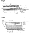
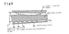
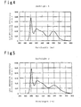
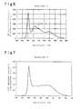

Classifications
-
- G—PHYSICS
- G02—OPTICS
- G02B—OPTICAL ELEMENTS, SYSTEMS OR APPARATUS
- G02B5/00—Optical elements other than lenses
- G02B5/20—Filters
-
- G—PHYSICS
- G02—OPTICS
- G02B—OPTICAL ELEMENTS, SYSTEMS OR APPARATUS
- G02B6/00—Light guides; Structural details of arrangements comprising light guides and other optical elements, e.g. couplings
- G02B6/0001—Light guides; Structural details of arrangements comprising light guides and other optical elements, e.g. couplings specially adapted for lighting devices or systems
- G02B6/0011—Light guides; Structural details of arrangements comprising light guides and other optical elements, e.g. couplings specially adapted for lighting devices or systems the light guides being planar or of plate-like form
- G02B6/0033—Means for improving the coupling-out of light from the light guide
- G02B6/0035—Means for improving the coupling-out of light from the light guide provided on the surface of the light guide or in the bulk of it
- G02B6/0038—Linear indentations or grooves, e.g. arc-shaped grooves or meandering grooves, extending over the full length or width of the light guide
-
- C—CHEMISTRY; METALLURGY
- C09—DYES; PAINTS; POLISHES; NATURAL RESINS; ADHESIVES; COMPOSITIONS NOT OTHERWISE PROVIDED FOR; APPLICATIONS OF MATERIALS NOT OTHERWISE PROVIDED FOR
- C09B—ORGANIC DYES OR CLOSELY-RELATED COMPOUNDS FOR PRODUCING DYES, e.g. PIGMENTS; MORDANTS; LAKES
- C09B67/00—Influencing the physical, e.g. the dyeing or printing properties of dyestuffs without chemical reactions, e.g. by treating with solvents grinding or grinding assistants, coating of pigments or dyes; Process features in the making of dyestuff preparations; Dyestuff preparations of a special physical nature, e.g. tablets, films
- C09B67/0033—Blends of pigments; Mixtured crystals; Solid solutions
-
- C—CHEMISTRY; METALLURGY
- C09—DYES; PAINTS; POLISHES; NATURAL RESINS; ADHESIVES; COMPOSITIONS NOT OTHERWISE PROVIDED FOR; APPLICATIONS OF MATERIALS NOT OTHERWISE PROVIDED FOR
- C09B—ORGANIC DYES OR CLOSELY-RELATED COMPOUNDS FOR PRODUCING DYES, e.g. PIGMENTS; MORDANTS; LAKES
- C09B67/00—Influencing the physical, e.g. the dyeing or printing properties of dyestuffs without chemical reactions, e.g. by treating with solvents grinding or grinding assistants, coating of pigments or dyes; Process features in the making of dyestuff preparations; Dyestuff preparations of a special physical nature, e.g. tablets, films
- C09B67/006—Preparation of organic pigments
- C09B67/0063—Preparation of organic pigments of organic pigments with only macromolecular substances
- C09B67/0064—Preparation of organic pigments of organic pigments with only macromolecular substances of phthalocynanines with only macromolecular substances
-
- C—CHEMISTRY; METALLURGY
- C09—DYES; PAINTS; POLISHES; NATURAL RESINS; ADHESIVES; COMPOSITIONS NOT OTHERWISE PROVIDED FOR; APPLICATIONS OF MATERIALS NOT OTHERWISE PROVIDED FOR
- C09D—COATING COMPOSITIONS, e.g. PAINTS, VARNISHES OR LACQUERS; FILLING PASTES; CHEMICAL PAINT OR INK REMOVERS; INKS; CORRECTING FLUIDS; WOODSTAINS; PASTES OR SOLIDS FOR COLOURING OR PRINTING; USE OF MATERIALS THEREFOR
- C09D17/00—Pigment pastes, e.g. for mixing in paints
-
- C—CHEMISTRY; METALLURGY
- C09—DYES; PAINTS; POLISHES; NATURAL RESINS; ADHESIVES; COMPOSITIONS NOT OTHERWISE PROVIDED FOR; APPLICATIONS OF MATERIALS NOT OTHERWISE PROVIDED FOR
- C09K—MATERIALS FOR MISCELLANEOUS APPLICATIONS, NOT PROVIDED FOR ELSEWHERE
- C09K11/00—Luminescent, e.g. electroluminescent, chemiluminescent materials
- C09K11/08—Luminescent, e.g. electroluminescent, chemiluminescent materials containing inorganic luminescent materials
- C09K11/0883—Arsenides; Nitrides; Phosphides
-
- C—CHEMISTRY; METALLURGY
- C09—DYES; PAINTS; POLISHES; NATURAL RESINS; ADHESIVES; COMPOSITIONS NOT OTHERWISE PROVIDED FOR; APPLICATIONS OF MATERIALS NOT OTHERWISE PROVIDED FOR
- C09K—MATERIALS FOR MISCELLANEOUS APPLICATIONS, NOT PROVIDED FOR ELSEWHERE
- C09K11/00—Luminescent, e.g. electroluminescent, chemiluminescent materials
- C09K11/08—Luminescent, e.g. electroluminescent, chemiluminescent materials containing inorganic luminescent materials
- C09K11/77—Luminescent, e.g. electroluminescent, chemiluminescent materials containing inorganic luminescent materials containing rare earth metals
- C09K11/7728—Luminescent, e.g. electroluminescent, chemiluminescent materials containing inorganic luminescent materials containing rare earth metals containing europium
- C09K11/7729—Chalcogenides
- C09K11/7731—Chalcogenides with alkaline earth metals
-
- C—CHEMISTRY; METALLURGY
- C09—DYES; PAINTS; POLISHES; NATURAL RESINS; ADHESIVES; COMPOSITIONS NOT OTHERWISE PROVIDED FOR; APPLICATIONS OF MATERIALS NOT OTHERWISE PROVIDED FOR
- C09K—MATERIALS FOR MISCELLANEOUS APPLICATIONS, NOT PROVIDED FOR ELSEWHERE
- C09K11/00—Luminescent, e.g. electroluminescent, chemiluminescent materials
- C09K11/08—Luminescent, e.g. electroluminescent, chemiluminescent materials containing inorganic luminescent materials
- C09K11/77—Luminescent, e.g. electroluminescent, chemiluminescent materials containing inorganic luminescent materials containing rare earth metals
- C09K11/7728—Luminescent, e.g. electroluminescent, chemiluminescent materials containing inorganic luminescent materials containing rare earth metals containing europium
- C09K11/77348—Silicon Aluminium Nitrides or Silicon Aluminium Oxynitrides
-
- C—CHEMISTRY; METALLURGY
- C09—DYES; PAINTS; POLISHES; NATURAL RESINS; ADHESIVES; COMPOSITIONS NOT OTHERWISE PROVIDED FOR; APPLICATIONS OF MATERIALS NOT OTHERWISE PROVIDED FOR
- C09K—MATERIALS FOR MISCELLANEOUS APPLICATIONS, NOT PROVIDED FOR ELSEWHERE
- C09K11/00—Luminescent, e.g. electroluminescent, chemiluminescent materials
- C09K11/08—Luminescent, e.g. electroluminescent, chemiluminescent materials containing inorganic luminescent materials
- C09K11/77—Luminescent, e.g. electroluminescent, chemiluminescent materials containing inorganic luminescent materials containing rare earth metals
- C09K11/7766—Luminescent, e.g. electroluminescent, chemiluminescent materials containing inorganic luminescent materials containing rare earth metals containing two or more rare earth metals
- C09K11/7774—Aluminates
-
- C—CHEMISTRY; METALLURGY
- C09—DYES; PAINTS; POLISHES; NATURAL RESINS; ADHESIVES; COMPOSITIONS NOT OTHERWISE PROVIDED FOR; APPLICATIONS OF MATERIALS NOT OTHERWISE PROVIDED FOR
- C09K—MATERIALS FOR MISCELLANEOUS APPLICATIONS, NOT PROVIDED FOR ELSEWHERE
- C09K11/00—Luminescent, e.g. electroluminescent, chemiluminescent materials
- C09K11/08—Luminescent, e.g. electroluminescent, chemiluminescent materials containing inorganic luminescent materials
- C09K11/77—Luminescent, e.g. electroluminescent, chemiluminescent materials containing inorganic luminescent materials containing rare earth metals
- C09K11/7766—Luminescent, e.g. electroluminescent, chemiluminescent materials containing inorganic luminescent materials containing rare earth metals containing two or more rare earth metals
- C09K11/77742—Silicates
-
- G—PHYSICS
- G02—OPTICS
- G02B—OPTICAL ELEMENTS, SYSTEMS OR APPARATUS
- G02B5/00—Optical elements other than lenses
- G02B5/20—Filters
- G02B5/201—Filters in the form of arrays
-
- G—PHYSICS
- G02—OPTICS
- G02B—OPTICAL ELEMENTS, SYSTEMS OR APPARATUS
- G02B6/00—Light guides; Structural details of arrangements comprising light guides and other optical elements, e.g. couplings
- G02B6/0001—Light guides; Structural details of arrangements comprising light guides and other optical elements, e.g. couplings specially adapted for lighting devices or systems
- G02B6/0011—Light guides; Structural details of arrangements comprising light guides and other optical elements, e.g. couplings specially adapted for lighting devices or systems the light guides being planar or of plate-like form
- G02B6/0033—Means for improving the coupling-out of light from the light guide
- G02B6/005—Means for improving the coupling-out of light from the light guide provided by one optical element, or plurality thereof, placed on the light output side of the light guide
- G02B6/0053—Prismatic sheet or layer; Brightness enhancement element, sheet or layer
-
- G—PHYSICS
- G02—OPTICS
- G02F—OPTICAL DEVICES OR ARRANGEMENTS FOR THE CONTROL OF LIGHT BY MODIFICATION OF THE OPTICAL PROPERTIES OF THE MEDIA OF THE ELEMENTS INVOLVED THEREIN; NON-LINEAR OPTICS; FREQUENCY-CHANGING OF LIGHT; OPTICAL LOGIC ELEMENTS; OPTICAL ANALOGUE/DIGITAL CONVERTERS
- G02F1/00—Devices or arrangements for the control of the intensity, colour, phase, polarisation or direction of light arriving from an independent light source, e.g. switching, gating or modulating; Non-linear optics
- G02F1/01—Devices or arrangements for the control of the intensity, colour, phase, polarisation or direction of light arriving from an independent light source, e.g. switching, gating or modulating; Non-linear optics for the control of the intensity, phase, polarisation or colour
- G02F1/13—Devices or arrangements for the control of the intensity, colour, phase, polarisation or direction of light arriving from an independent light source, e.g. switching, gating or modulating; Non-linear optics for the control of the intensity, phase, polarisation or colour based on liquid crystals, e.g. single liquid crystal display cells
- G02F1/133—Constructional arrangements; Operation of liquid crystal cells; Circuit arrangements
- G02F1/1333—Constructional arrangements; Manufacturing methods
- G02F1/1335—Structural association of cells with optical devices, e.g. polarisers or reflectors
- G02F1/133509—Filters, e.g. light shielding masks
- G02F1/133514—Colour filters
-
- G—PHYSICS
- G02—OPTICS
- G02F—OPTICAL DEVICES OR ARRANGEMENTS FOR THE CONTROL OF LIGHT BY MODIFICATION OF THE OPTICAL PROPERTIES OF THE MEDIA OF THE ELEMENTS INVOLVED THEREIN; NON-LINEAR OPTICS; FREQUENCY-CHANGING OF LIGHT; OPTICAL LOGIC ELEMENTS; OPTICAL ANALOGUE/DIGITAL CONVERTERS
- G02F1/00—Devices or arrangements for the control of the intensity, colour, phase, polarisation or direction of light arriving from an independent light source, e.g. switching, gating or modulating; Non-linear optics
- G02F1/01—Devices or arrangements for the control of the intensity, colour, phase, polarisation or direction of light arriving from an independent light source, e.g. switching, gating or modulating; Non-linear optics for the control of the intensity, phase, polarisation or colour
- G02F1/13—Devices or arrangements for the control of the intensity, colour, phase, polarisation or direction of light arriving from an independent light source, e.g. switching, gating or modulating; Non-linear optics for the control of the intensity, phase, polarisation or colour based on liquid crystals, e.g. single liquid crystal display cells
- G02F1/133—Constructional arrangements; Operation of liquid crystal cells; Circuit arrangements
- G02F1/1333—Constructional arrangements; Manufacturing methods
- G02F1/1335—Structural association of cells with optical devices, e.g. polarisers or reflectors
- G02F1/1336—Illuminating devices
- G02F1/133617—Illumination with ultraviolet light; Luminescent elements or materials associated to the cell
-
- G—PHYSICS
- G02—OPTICS
- G02F—OPTICAL DEVICES OR ARRANGEMENTS FOR THE CONTROL OF LIGHT BY MODIFICATION OF THE OPTICAL PROPERTIES OF THE MEDIA OF THE ELEMENTS INVOLVED THEREIN; NON-LINEAR OPTICS; FREQUENCY-CHANGING OF LIGHT; OPTICAL LOGIC ELEMENTS; OPTICAL ANALOGUE/DIGITAL CONVERTERS
- G02F1/00—Devices or arrangements for the control of the intensity, colour, phase, polarisation or direction of light arriving from an independent light source, e.g. switching, gating or modulating; Non-linear optics
- G02F1/01—Devices or arrangements for the control of the intensity, colour, phase, polarisation or direction of light arriving from an independent light source, e.g. switching, gating or modulating; Non-linear optics for the control of the intensity, phase, polarisation or colour
- G02F1/13—Devices or arrangements for the control of the intensity, colour, phase, polarisation or direction of light arriving from an independent light source, e.g. switching, gating or modulating; Non-linear optics for the control of the intensity, phase, polarisation or colour based on liquid crystals, e.g. single liquid crystal display cells
- G02F1/133—Constructional arrangements; Operation of liquid crystal cells; Circuit arrangements
- G02F1/1333—Constructional arrangements; Manufacturing methods
- G02F1/1335—Structural association of cells with optical devices, e.g. polarisers or reflectors
- G02F1/1336—Illuminating devices
- G02F1/133621—Illuminating devices providing coloured light
Definitions
- the present invention relates to a blue composition for a color filter, a color filter and a color image display device. Particularly, it relates to a blue composition for a color filter to realize an image having a high color purity corresponding to the emission wavelength of an improved LED backlight, a color filter and a color image display device.
- the color gamut of color liquid crystal display elements is determined by chromaticity of light emitted from red, green and blue pixels and, where chromaticity points of the respective color pixels in CIE system of color representation are represented by (x R , y R ), (X G , y G ), (x B , x B ), the color gamut is defined by an area of a triangle surrounded by these three points on a x-y chromaticity diagram. Namely, the larger the area of this triangle, the more vivid color image the display elements reproduce.
- the area of this triangle is usually expressed using a ratio of the area of the triangle to the area of a reference triangle formed by three points of the three primary colors, red (0.67,0.33), green (0.21,0.71) and blue (0.14,0.08), in the standard system defined by US National Television System Committee (NTSC) (in unit of %, hereinafter referred to simply as "NTSC percentage").
- NTSC National Television System Committee
- Ordinary notebook computers have the values of approximately 40 to 50%, desktop computer monitors the values of 50 to 60%, and existing liquid crystal TVs the values of approximately 70%.
- a color image display device utilizing such color liquid display elements is mainly composed of light bulbs utilizing liquid crystal, a color filter having red, green and blue pixels, and a backlight for transmission illumination, and the chromaticity of light emitted from the red, green and blue pixels are determined by the emission wavelengths of the backlight and the transmittance spectrum of the color filter.
- the color filter extracts only wavelengths in necessary regions from the emission distribution of the backlight to provide the red, green and blue pixels.
- Methods for production of this color filter proposed heretofore include such methods as dying, pigment dispersion, electro-deposition, printing, inkjet, and so on.
- the colorant for coloring used to be dyes but are now pigments in terms of reliability and durability as liquid crystal display elements. Accordingly, the pigment dispersion is most commonly used as a method for production of the color filter at present in terms of productivity and performance.
- the NTSC percentage and brightness are in a trade-off relation and are appropriately used according to applications.
- the backlight generally used is one using as a light source a cold cathode fluorescent lamp with emission wavelengths in the red, green and blue wavelength regions and using a light guide plate for converting a light emitted from this cold cathode fluorescent lamp into white area light source.
- a LED is becoming used from such a viewpoint that it has a long life, it requires no inverter, it provides a high brightness and it is free from mercury.
- a conventional LED backlight uses blue light emitted from a LED and a yellow phosphor obtained by excitation using the blue light as a white area light source.
- the above-described light source employs a yellow phosphor, and thus there are a great deal of emission of lights, with unnecessary wavelengths in terms of the color purities of red and green, and it has been difficult to obtain a high gamut display.
- As a countermeasure it is possible to cut out lights with unnecessary wavelengths by a color filter to increase the color purities of red and green in principle, but most part of emission from the backlight is cut out, and thus the brightness will significantly decrease. Particularly by this method, red emission will significantly decrease, and accordingly it is practically impossible to reproduce a strongly reddish color.
- the emission wavelength distribution of a LED has such characteristics that the emission intensity is high in a range of from 460 to 480 nm as compared with that of a cold cathode fluorescent lamp.
- the light in this wavelength region deteriorates the color purity of a blue pixel and thereby is required to be cut out by a blue color filter as far as possible.
- a conventional blue composition for a color filter hereinafter sometimes referred to simply as a blue composition or a blue resist
- a color filter have not had sufficient performance to cut out lights with wavelengths of from 460 to 480 nm, and are not sufficiently suitable for a color image display device using a LED as a backlight:
- Non Patent Document 1 a method of combining a LED which emits red, green and blue lights has been proposed (Non Patent Document 1) in recent years, and a display having an extremely high gamut has been produced experimentally by this method.
- red, green and blue LED chips are independently assembled, there are such problems that 1) mounting takes effort, 2) red, green and blue LED chips are disposed with limited distances, and thus the distance from the respective LED chips to a light guide plate is required to be long for sufficient color mixture of emission from the respective LED chips, and 3) integral multiple numbers of the respective LED chips are combined to adjust the white chromaticity, and thus the white balance cannot continuously be adjusted.
- Non Patent Document 1 Monthly DISPLAY April 2003, p.42 to 46
- the present inventors have conducted extensive studies and as a result, found it possible to realize an image having a high color purity, by improving the emission wavelength of a backlight and by adjusting the transmittance of a color filter correspondingly to the emission wavelength of the backlight as well.
- the present invention has been made based on the above discovery, and provides the following (A) to (K).
- such a color liquid crystal display device can be provided that reproduction of a deep red and green image can be realized without sacrifice of the brightness of the image even with a LED backlight, and high gamut over the entire image can be achieved, and further, red, green and blue emission is achieved by one chip, whereby productivity in mounting will not be impaired, and the white balance can be easily adjusted.
- Embodiments of the blue composition for a color filter, the color filter and the color liquid crystal display device of the present invention will be described below. These are an example of the embodiments of the present invention, and the present invention is not limited thereto.
- the blue composition for a color filter of the present invention is a blue composition for a color filter, which comprises a binder resin (a) and/or a monomer (b) and a colorant (c), and is characterized in that its cured product has an average value T B (460-480) (%) of the spectrum transmittance at a wavelength at every interval of 5 nm in the visible light range of from 460 to 480 nm of at most 65%.
- a cured product of the blue composition of the present invention which has the above characteristics of the average spectrum transmittance, can shut off extra wavelengths in the blue region characteristic of a LED backlight, and further improves wide color gamut of the color image display device of the present invention as described in Chapter (3).
- T B (460-480) is preferably at most 60%, more preferably at most 58%. Further, it is usually at least 1%. If T B (460-480) is too high, lights with extra wavelengths characteristic of the LED backlight tends to be transmitted, thus impairing the color gamut. Further, if it is too low, even the transmittance of light in the vicinity of 450 nm as the main component for the blue color tends to decrease, thus decreasing the brightness of the blue pixel.
- composition of the blue composition of the present invention is not particularly limited so long as the blue composition has the above characteristics of the average spectral transmittance, but the characteristics can be secured by the following specific means.
- a blue composition containing as the colorant (c) a dioxazine violet pigment and/or a copper phthalocyanine pigment has the above characteristics of the average spectral transmittance.
- the dioxazine violet pigment may, for example, be pigments of the following pigment numbers. "C.I” indicates the color index (C.I.).
- the copper phthalocyanine pigment may, for example, be pigments of the following pigment numbers.
- the content of the dioxazine violet pigment to all the blue pigments is usually at least 25 wt%, preferably at least 30 wt%, more preferably at least 35 wt%. Further, it is usually at most 90 wt%. If the content of the dioxazine violet pigment is too low, T B (460-480) will be too high, whereby too greenish blue will be obtained, thus decreasing the color purity. Further, if the content is too high, the transmittance of light in the vicinity of 450 nm as the main component for the blue light tends to be too low, thus decreasing the brightness of the blue pixel.
- the content of the copper phthalocyanine pigment to all the pigments is usually at least 10 wt%. Further, it is usually at most 75 wt%, preferably at most 70 wt%, more preferably at most 65 wt%. If the content of the copper phthalocyanine pigment is too low, the pixel tends to provide a less bluish color, thus decreasing the color purity. Further, if the content is too high, T B (460-480) tends to be too high, whereby too greenish blue will be obtained, thus decreasing the color purity.
- the proportion of the content of the dioxazine violet pigment to the content of the copper phthalocyanine pigment is usually 25:75 to 75:25, preferably 30:70 to 70:30, more preferably 35:65 to 65:35. If the amount of the dioxazine violent pigment is too large as compared with the amount of the copper phthalocyanine pigment, the transmittance of light in the vicinity of 450 nm as the main component for the blue light tends to be too low, thus decreasing the brightness of the blue pixel.
- T B (460-480) tends to be too high, whereby too greenish blue will be obtained, thus decreasing the color purity.
- the color filter of the present invention is characterized by having a pixel formed by the above blue composition.
- the color filter of the present invention can shut off extra wavelengths in the blue region characteristic of a LED backlight and further improve the wide color gamut of the color image display device of the present invention as described in Chapter (3).
- the blue pixel of the color filter of the present invention has an average value T B (460-480) (%) of the spectral transmittance at a wavelength at every interval of 5 nm in the visible light range of from 460 to 480 nm of usually at most 65%, preferably at most 60%, more preferably at most 58%. Further, it is usually at least 1%.
- T B (460-480) is too high, lights with extra wavelengths characteristic of the LED backlight tend to be transmitted, thus impairing the color gamut. Further, if it is too low, even the transmittance of light in the vicinity of 450 nm as the main component for the blue color tends to decrease, thus decreasing the brightness of the blue pixel.
- the blue composition preferably contains a dioxazine violet pigment, and its content is as described in Chapter (1).
- the content V (%) of the dioxazine violet pigment to the total solid content and the film thickness T ( ⁇ m) after drying preferably satisfy the following formula: VT ⁇ 10
- VT is preferably at least 11, more preferably at least 12, and it is usually at most 90. If the value of VT is too small, T B (460-480) tends to be too high, whereby too greenish blue will be obtained, thus decreasing the color purity, and if it is too high, the transmittance of light in the vicinity of 450 nm as the main component for the blue color tends to decrease, thus decreasing the brightness of the blue pixel.
- the color image display device of the present invention comprises a combination of light bulbs, a color filter having color elements of at least three colors of red, green and blue corresponding to the light bulbs, and a backlight for transmission illumination, and its specific structure is not particularly limited.
- a color liquid crystal display device of a TFT type wherein the light bulbs employ liquid crystal as shown in Fig. 1 may be mentioned.
- Fig. 1 shows an example of the color liquid crystal display device of a TFT (thin film transistor) type using a side-light type backlight device and a color filter.
- TFT thin film transistor
- a liquid crystal display device In this liquid crystal display device, light emitted from a light source 1 is converted into an area light source by a light guide plate 2, a light diffuser sheet 3 further enhances uniformity of the light, and the light then passes a prism sheet to enter a polarizer 4. For this incident light, a direction of polarization is controlled in each pixel by TFT 6 and thereafter the light is incident into a color filter 9. Finally, the light passes through a polarizer 10 with the direction of polarization perpendicular to that of the polarizer 4 and then reaches an observer. The degree of change of the polarization direction of the incident light varies depending upon an applied voltage to TFT 6, so as to change the quantity of light passing through the polarizer 10, thus enabling display of a color image.
- Numerals 5 and 8 denote transparent substrates (glass substrates), and 7 a liquid crystal.
- the color image display device of the present invention is characterized by having wide color gamut by the structure as described in detail below.
- the color image display device of the present invention comprises a combination of light bulbs, a color filter having color elements of at least three colors of red, green and blue corresponding to the light bulbs, and the backlight for transmission illumination, and is characterized in that a light source for the backlight comprises a combination of a blue or deep blue LED and a phosphor and has at least one main component for emission in each of the wavelength regions of from 430 to 470 nm, from 500 to 540 nm and from 600 to 680 nm, and a color image display element has a color gamut of the NTSC percentage of at least 60%.
- the NTSC percentage is preferably at least 70%.
- the color temperature of the color image display device of the present invention is usually from 5,000 to 10,000 K, preferably from 5,500 to 9,500 K, more preferably from 6,000 to 9,000 K. If the color temperature is too low, an entirely reddish image will be obtained, and if the color temperature is too high, the brightness tends to decrease.
- the backlight device used in the present invention is an area light source device disposed on a back face of a liquid crystal panel and used as a back light source means for a transmission type or semi-transmission type color liquid crystal display device.
- the backlight device comprises a LED which emits white light, and a light unformalizing means for converting the light-source light into a nearly uniform area light source.
- Typical examples of installation of the light source include a method of placing the light source immediately below the backlight of the liquid crystal elements (direct backlight system) and a method of placing the light source on a side face and using an optically transparent light guide such as an acrylic plate to convert the light into area light to obtain an area light source (side light system).
- the side light system as shown in Figs. 2 and 3 is suitably applicable as an area light source being thin and excellent in uniformity of luminance distribution, and is now most commonly put to practical use.
- the backlight device of Fig. 2 is configured so that a light emitting diode 1 is placed along one side end face 11a of a substrate consisting of an optically transparent flat plate, i.e. a light guide 11, and light is made incident through one side end face 11a as a light entrance face into the interior of the light guide 11.
- a light control sheet 13 with an array 12 of nearly triangle prism shape formed therein is place above the light exit face 11b so that apex angles of the array 12 are directed toward the observer.
- a light extracting mechanism 14 printed in a predetermined pattern of many dots 14a of light scattering ink is provided on the other face 11c opposite to the light exit face 11b in the light guide 11.
- a reflecting sheet 15 is provided in proximity to this face 11c.
- the backlight device of Fig. 3 is constructed in much the same configuration as the backlight device shown in Fig. 2 , except that the light control sheet 13 with the prism array 12 of nearly triangle prism shape formed therein is located so that the apex angles of the array 12 are directed toward the light exit face 11b of the light guide 11 and except that the light extracting mechanism 14' provided in the face 11c opposite to the light exit face 11b of the light guide 11 comprises a rough pattern 14b with each surface being formed as the rough surface.
- the light source of the backlight device of the present invention is characterized by containing a LED (hereinafter sometimes referred to as a light emitting diode optionally) in its structure.
- the light source can be any light source of the type providing emissions in the red, green and blue wavelength regions, i.e. in ranges of from 580 to 700 nm, from 500 to 550 nm, and from 400 to 480 nm.
- the light source comprises a combination of a blue or deep blue LED and a phosphor, and is adjusted so that there is at least one main component for emission in each of the wavelength regions of the red region (usually from 600 to 680 nm, preferably from 610 to 680 nm, more preferably from 620 to 680 nm), the green region (usually from 500 to 540 nm, preferably from 500 to 530 nm, more preferably from 500 to 525 nm) and the blue region (usually from 430 to 470 nm, preferably from 440 to 460 nm).
- the red region usually from 600 to 680 nm, preferably from 610 to 680 nm, more preferably from 620 to 680 nm
- the green region usually from 500 to 540 nm, preferably from 500 to 530 nm, more preferably from 500 to 525 nm
- the blue region usually from 430 to 470 nm, preferably from 440 to 460 nm.
- the quantity of light in the respective red, green and blue regions at a transmission type or semi-transmission type transmission mode is determined by the product of the emission from the backlight and the spectral transmittance of the color filter. Accordingly, it is necessary to select such a backlight as to satisfy conditions as described in the item (c) colorant of the composition for a color filter.
- backlight device of the present invention will be described below, but the backlight light source of the present invention is not limited thereto so long as the above conditions are met.
- the light source is preferably a light emitting diode.
- the emission wavelength of the light source is from 440 to 490 nm, preferably from 450 nm to 480 nm.
- the light source for example, InGaN, GaAlN, InGaAlN, ZnSeS semiconductor having crystals grown by e.g. a MOCVD method on a substrate of e.g. silicon carbide, sapphire or gallium nitride, is suitable.
- a plurality of the light sources may be used so as to obtain a high output.
- the light source may be an end face emission type or face emission type laser diode.
- a frame to fix the light source has at least positive and negative electrodes to supply electricity to the light source.
- a concave cup may be formed on the frame, and the light source is disposed on the bottom, whereby the emitted light can be made to have directivity, and light can be effectively utilized.
- the inner face of the concave portion of the frame or the entire frame may be plated with a high reflective metal such as silver, platinum or aluminum or an alloy equal thereto, whereby the reflectance in the overall visible light range can be increased, and the efficiency of light can be increased. Further, the same effects will be obtained when the surface of the concave portion of the frame or the entire frame is made of a resin for injection molding, containing white glass fibers or a high reflective substance such as an alumina powder or a titania powder.
- an epoxy, imide, acrylic or another adhesive or a solder such as AuSn or AgSn is used.
- an adhesive When electricity is supplied to the light source via an adhesive, it is preferred to thinly and uniformly coat one having an electrically conductive filler such as fine silver particles incorporated in an adhesive, such as a silver paste or a carbon paste.
- an adhesive such as a silver paste or a carbon paste.
- a solder is effective for a large electric current type light emitting diode or laser diode of which heat dispersion properties are important.
- any adhesive may be employed for fixation of a light source to which no electricity will be applied through an adhesive, but a silver paste or a solder is preferred considering heat dispersion properties.
- the light source and the electrode of the frame are connected by wire bonding.
- a wire a gold or aluminum wire having a diameter of from 20 to 40 ⁇ m is used.
- a method employing flip chip bonding without using a wire may also be employed.
- a phosphor emitting light in a green band and a phosphor emitting light in a red band are mixed with a transparent binder such as an epoxy resin or a silicone resin and coated on a light emitting diode.
- the proportion of mixing may optionally be changed so as to obtain a desired chromaticity.
- the phosphor emitting light in a green band and the phosphor emitting light in a red band may be separately coated on a light emitting diode.
- a dispersing agent is further added to the transparent binder, the emitted light can be made more uniform.
- the dispersing agent is preferably a colorless substance having an average particle size of from 100 nm to several dozen ⁇ m.
- Alumina, zirconia, yttria and the like are preferred since they are stable at a temperature range of from -60 to 120°C at which they are used.
- a dispersing agent having a high refractive index is more preferred, which provides a higher effect.
- the light emitting diode When electricity is applied to a finished light emitting device, first, the light emitting diode emits a blue or deep blue light.
- the phosphor absorbs part of the light and emits a light in a green band or in a red band.
- a substantially white light is obtained, formed by mixing the original light in a blue band from the light emitting diode and lights in a green band and in a red band, the wavelengths of which are converted by the phosphor.
- the phosphor will be explained below.
- the above-described backlight has a phosphor layer or a phosphor film, and the phosphor layer or the phosphor film employs the following phosphor.
- red phosphor used for the phosphor layer or the phosphor film to be used for the color liquid crystal display device of the present invention various phosphors having an emission peak wavelength within a wavelength range of 620 nm ⁇ n ⁇ 680 nm can be used.
- a phosphor activated with europium is preferred.
- the phosphor activated with europium may be nitride phosphor, an oxynitride phosphor, a sulfide phosphor or an oxysulfide phosphor, and among them, preferred is a nitride phosphor or an oxynitride phosphor.
- the chemical formula weight a of Eu in the formula (3) is preferably within a range of 0.0002 ⁇ a ⁇ 0.02, more preferably 0.0004 ⁇ a ⁇ 0.02.
- the chemical formula weight a of Eu in the formula (3) is preferably within a range of 0.0004 ⁇ a ⁇ 0.01, more preferably 0.0004 ⁇ a ⁇ 0.007, furthermore preferably 0.0004 ⁇ a ⁇ 0.005, still more preferably 0.0004 ⁇ a ⁇ 0.004.
- the chemical formula a of Eu in the formula (3) is preferably within a range of 0.0004 ⁇ a ⁇ 0.02, more preferably 0.001 ⁇ a ⁇ 0.008. If the content of the emission center ion Eu 2+ is too low, the emission intensity tends to be low, and if it is too high, the emission intensity also tends to decrease due to a phenomenon called concentration quenching.
- the preferred range of the chemical formula weight a of Eu in the formula (3) which satisfies all the heat stability, the temperature characteristics and the emission intensity it is preferably within a range of 0.0004 ⁇ a ⁇ 0.004, more preferably 0.001 ⁇ a ⁇ 0.004.
- the molar ratio of the cation site occupied by Eu, Ca, Sr and M and the anion site occupied by S is 1:1, but the aimed phosphor performance will not significantly be influenced even when a cation defect or an anion defect somewhat occurs, and accordingly, a basic crystal of the above formula (3) with a molar ratio e of the anion site occupied by S within a range of at least 0.9 and at most 1.1 can be used.
- M representing at least one element selected from Ba, Mg, and Zn is not necessarily essential in the present invention, but the object of the present invention can be achieved even when it is contained in the chemical substance of the above formula (3) with a molar ratio d of M within a range of 0 ⁇ d ⁇ 0.1.
- a compound containing at least element M 4 , element A, element D, element E and element X (wherein M 4 is one or at least two elements selected from the group consisting of Mn, Ce, Pr, Nd, Sm, Eu, Tb, Dy, Ho, Er, Tm and Yb and contains at least Eu, A is one or at least two elements selected from the group consisting of bivalent metal elements other than the element M 4 , D is one or at least two elements selected from the group consisting of tetravalent metal elements, E is one or at least two elements selected from the group consisting of trivalent metal elements, and X is one or at least two elements selected from the group consisting of O, N and F).
- M 4 is one or at least two elements selected from the group consisting of Mn, Ce, Pr, Nd, Sm, Eu, Tb, Dy, Ho, Er, Tm and Yb and contains at least Eu
- A is one or at least two elements selected from the group consisting of bivalent metal elements other than the element M 4
- D
- the above compound is particularly preferred from such a viewpoint that a light emitting element is less likely to deteriorate during its use, and the change in brightness due to a change in the temperature at which the light emitting element is used is small, whereby a high brightness and high color rendering light emitting element can be obtained.
- M 4 is one or at least two elements selected from the group consisting of Mn, Ce, Pr, Nd, Sm, Eu, Tb, Dy, Ho, Er, Tm and Yb and contains at least Eu, and among them, it is preferably one or at least two elements selected from the group consisting of Mn, Ce, Sm, Eu, Tb, Dy, Er, and Yb, and it is more preferably Eu.
- A is one or at least two elements selected from the group consisting of bivalent metal elements other than the element M 4 , and among them, it is preferably one or at least two elements selected from the group consisting of Mg, Ca, Sr and Ba, more preferably Ca.
- D is one or at least two elements selected from the group consisting of tetravalent metal elements, and among them, it is preferably one or at least two elements selected from the group consisting of Si, Ge, Sn, Ti, Zr and Hf, more preferably Si.
- E is one or at least two elements selected from the group consisting of trivalent metal elements, and among them, it is preferably one or at least two elements selected from the group consisting of B, Al, Ga, In, Sc, Y, La, Gd and Lu, more preferably Al.
- X is one or at least two elements selected from the group consisting of O, N and F, and among them, it is preferably N, or N and O.
- the value f is preferably at least 0.002 and at most 0.03 in view of high emission brightness.
- a preferred composition with high emission brightness is an inorganic compound wherein at least the element M 4 contains Eu, the element A contains Ca, the element D contains Si, the element E contains Al and the element X contains N.
- it is an inorganic compound wherein the element M 4 is Eu, the element A is Ca, the element D is Si, the element E is Al and the element X is N or a mixture of N and O.
- the emission intensity tends to decrease if (the number of moles of O) / (the number of moles of N + the number of moles of O) is too high.
- (the number of moles of O)/(the number of moles of N + the number of moles of O) is preferably at most 0.5, more preferably at most 0.3, and furthermore preferably at most 0.1, whereby a red phosphor with favorable color purity, having an emission peak wavelength in an emission wavelength of from 640 to 660 nm will be obtained.
- a green phosphor used for the phosphor layer or the phosphor film to be used for the color liquid crystal display device of the present invention various phosphors having an emission peak wavelength within a wavelength range of 500 nm ⁇ n ⁇ 530 nm can be used.
- Such a green phosphor to realize an image with high color purity preferably contains a phosphor activated with cerium and/or europium.
- the phosphor activated with cerium and/or europium may be an oxide phosphor, a nitride phosphor or an oxynitride phosphor, and among them, preferred is an oxide phosphor activated with cerium or an oxynitride phosphor activated with europium.
- a phosphor having a garnet crystal structure as the crystal structure is preferred, which tends to be excellent in view of e.g. heat resistance.
- a compound represented by the formula (7) comprising a complex oxide containing bivalent, trivalent and tetravalent metal elements as the host material and containing at least Ce as an activator element in the host material: M 1 a ,M 2 b ,M 3 c ,O d, (7) wherein M 1 , M 2 and M 3 represent a bivalent metal element, a trivalent metal element and a tetravalent metal element, respectively, and a' to d' are numerical values within the following ranges: 2.7 ⁇ a ⁇ ⁇ 3.3 1.8 ⁇ b ⁇ ⁇ 2.2 2.7 ⁇ c ⁇ ⁇ 3.3 11.0 ⁇ d ⁇ ⁇ 13.0
- M 1 is a bivalent metal element, and in view of e.g. the emission efficiency, it is preferably at least one element selected from the group consisting of Mg, Ca, Zn, Sr, Cd and Ba, more preferably Mg, Ca or Zn, particularly preferably Ca.
- Ca may be a simple substance or a complex with Mg.
- M 1 preferably comprises the above preferred element, but may contain another bivalent metal element within a range not to impair the performance.
- M 2 is a trivalent metal element, and from a similar viewpoint, it is preferably at least one element selected from the group consisting of Al, Sc, Ga, Y, In, La, Gd and Lu, more preferably Al, Sc, Y or Lu, particularly preferably Sc.
- Sc may be a simple substance or a complex with Y or Lu.
- M 2 preferably comprises the above preferred element but may contain another trivalent metal element within a range not to impair the performance.
- M 3 is a tetravalent metal element, and from a similar viewpoint, it preferably contains at least Si, and usually at least 50 mol%, preferably at least 70 mol%, more preferably at least 80 mol%, particularly preferably at least 90 mol%, of the tetravalent metal element represented by M 3 is Si.
- the tetravalent metal element M 3 other than Si is preferably at least one element selected from the group consisting of Ti, Ge, Zr, Sn and Hf, more preferably at least one element selected from the group consisting of Ti, Zr, Sn and Hf, particularly preferably Sn.
- M 3 is Si.
- M 3 preferably comprises the above preferred element, but may contain another tetravalent metal element within a range not to impair the performance.
- containing another element within a range not to impair the performance means that such an element is contained in an amount of usually at most 10 mol%, preferably at most 5 mol%, more preferably at most 1 mol%, based on each of the M 1 , M 2 , and M 3 .
- a', b', c' and d' are numerical values within ranges of 2.7 ⁇ a' ⁇ 3.3, 1.8 ⁇ b' ⁇ 2.2, 2.7 ⁇ c' ⁇ 3.3 and 11.0 ⁇ d' ⁇ 13.0.
- a' to d' of the present phosphor vary within the above ranges in accordance with whether the emission center ion element replaces the position of the crystal lattice of any one of the metal elements M 1 , M 2 , and M 3 or it is interstitially disposed.
- the emission center ion (activator element) contained in the host material of this crystal structure at least Ce is contained, but at least one bivalent to tetravalent element selected from the group consisting of Cr, Mn, Fe, Co, Ni, Cu, Pr, Nd, Sm, Eu, Tb, Dy, Ho, Er, Tm and Yb can be incorporated as a co-activator so as to finely adjust the emission characteristics.
- at least one bivalent to tetravalent element selected from the group consisting of Mn, Fe, Co, Ni, Cu, Sm, Eu, Tb, Dy and Yb can be incorporated, and bivalent Mn, bivalent or trivalent Eu or trivalent Tb can be suitably be added.
- the amount of the co-activator is usually from 0.01 to 20 mol per mol of Ce.
- M 5 k M 6 1 M 7 m O n (8) wherein M 5 , M 6 and M 7 represent an activator element containing at least Ce, a bivalent metal element and a trivalent metal element, respectively, and k to n are numerical values within the following ranges: 0.0001 ⁇ k ⁇ 0.2 0.8 ⁇ l ⁇ 1.2 1.6 ⁇ m ⁇ 2.4 3.2 ⁇ n ⁇ 4.8
- M 5 is an activator element to be incorporated in the crystal host material as described hereinafter and contains at least Ce, and at least one bivalent to tetravalent element selected from the group consisting of Cr, Mn, Fe, Co, Ni, Cu, Ce, Pr, Nd, Sm, Eu, Tb, Dy, Ho, Er, Tm and Yb can be incorporated as a co-activator for the purpose adjusting long persistent phosphorescence or chromaticity, increasing sensitivity, or the like.
- the amount of the co-activator is usually from 0.01 to 20 mol% per mol of Ce.
- the concentration k of the activator element M 5 is 0.0001 ⁇ k ⁇ 0.2. If the value k is too small, the amount of the emission center ion present in the crystal host material of the phosphor tends to be too small, and the emission intensity tends to be low. On the other hand, if the value k is too large, the emission intensity tends to be small due to the concentration quenching. Accordingly, in view of the emission intensity, k is preferably 0.0005 ⁇ k ⁇ 0.1, most preferably 0.002 ⁇ k ⁇ 0.04. Further, the emission peak wavelength tends to shift to the long wavelength side and the quantity of the green light with high eye spectral sensitivity relatively increases along with an increase in the Ce concentration. Accordingly, in view of the balance between the emission intensity and the emission peak wavelength, k is preferably 0.004 ⁇ k ⁇ 0.15, more preferably 0.008 ⁇ k ⁇ 0.1, most preferably 0.02 ⁇ k ⁇ 0.08.
- M 6 is a bivalent metal element, and in view of e.g. the emission efficiency, it is preferably at least one element selected from the group consisting of Mg, Ca, Zn, Sr, Cd and Ba, more preferably Mg, Ca or Sr, and it is particularly preferred that at least 50 mol% of the element M 6 is Ca.
- M 7 is a trivalent metal element, and from a similar viewpoint, it is preferably at least one element selected from the group consisting of Al, Sc, Ga, Y, In, La, Gd, Yb and Lu, more preferably Al, Sc, Yb or Lu, furthermore preferably Sc, or Sc and Al, or Sc and Lu, and it is particularly preferred that at least 50 mol% of the element M 7 is Sc.
- the host material crystal of the phosphor is commonly a crystal represented by a compositional formula M 6 M 7 2 O 4 comprising M 6 which is a bivalent metal element, M 7 which is a trivalent metal element and oxygen, and accordingly the chemical compositional ratio is commonly such that 1 is 1, m is 2 and n is 4 in the formula (8).
- M 6 which is a bivalent metal element
- M 7 which is a trivalent metal element and oxygen
- the chemical compositional ratio is commonly such that 1 is 1, m is 2 and n is 4 in the formula (8).
- 1, m and n are numerical values within ranges of 0.8 ⁇ l ⁇ 1.2, 1.6 ⁇ m ⁇ 2.4 and 3.2 ⁇ n ⁇ 4.8. Further, 1 and m are preferably numerical values within ranges of 0.9 ⁇ l ⁇ 1.1 and 1.8 ⁇ m ⁇ 2.2 and n is preferably within a range of 3.6 ⁇ n ⁇ 4.4.
- M 6 and M 7 represent bivalent and trivalent metal elements, respectively, but it is possible to replace a very small part of M 6 and/or M 7 with a monovalent, tetravalent or pentavalent metal element to adjust e.g. the charge balance so long as there is no essential difference in view of e.g. the emission characteristics or the crystal structure. Further, a very small amount of an anion such as a halogen element (F, Cl, Br or I), nitrogen, sulfur, or selenium may be contained in the compound.
- a halogen element F, Cl, Br or I
- This substance is excited by a light of from 420 to 480 nm, and most efficiently excited by a light of from 440 to 470 nm.
- the emission spectrum has a peak in a range of from 490 to 550 nm, and has a wavelength component in a range of from 450 to 700 nm.
- MSi 2 N 2 O 2 activated with europium wherein M is one or at least two types of alkaline earth metals
- ⁇ -SiAlON activated with europium disclosed in "Succeeded in development of green phosphor for white LED” as a paper for Tsukuba Science City Press Club, Education and Science Press Club and Science Press Club, published by National Institute for Material Science on March 23, 2005, may, for example, be mentioned.
- the color filter to be used for the color image display device of the present invention is not particularly limited, but the following one may be used for example. In such a case, it is preferred to use the color filter as disclosed in the above-described Chapter (2) characterized in the blue pixel of the color filter.
- the color filter is a filter obtained by forming fine pixels of red, green, blue and so on on a transparent substrate of glass or the like by a method of dyeing, printing, electrodeposition, pigment dispersion, or the like. In order to block leaking light between these pixels and obtain images with higher quality, it is often the case to provide a light shielding pattern called a black matrix between pixels.
- a color filter by dyeing is fabricated as follows: an image is formed by a photosensitive resin obtained by mixing a dichromate as a photosensitive agent into gelatin, polyvinyl alcohol, or the like, followed by dyeing.
- a color filter by printing is fabricated by transferring a heat-curing or photo-curing ink onto a transparent substrate of glass or the like by such a method as screen printing, gravure printing, flexographic printing, transfer printing or soft lithography (imprint lithography).
- a color filter by electrodeposition is formed by electrophoresis effected while a transparent substrate of glass or the like with an electrode thereon is immersed in a bath containing a pigment or a dye.
- a color filter by pigment dispersion is formed by applying a composition in which a colorant such as a pigment is dispersed or dissolved in a photosensitive resin, onto a transparent substrate of glass or the like to form a coating film thereon, exposing the coating film to radiation through a photomask to effect exposure, and removing unexposed portions by a development process to form a pattern.
- the color filter can also be fabricated by other methods than these, including a method of applying a polyimide type resin composition in which a colorant is dispersed or dissolved, and forming a pixel image by etching, a method of attaching a film coated with a resin composition containing a colorant, to a transparent substrate, peeling it off, and effecting image exposure and development to form a pixel image, a method of forming a pixel image by an ink jet printer, and so on.
- the pigment dispersion method is mainstream in fabrication of the color filters for liquid crystal display elements by virtue of its high productivity and excellent microfabrication property, but the color filter according to the present invention can be fabricated by any one of the above-mentioned production methods.
- Examples of methods of forming the black matrix include a method of forming a chromium and/or chromium oxide (single-layer or multi-layer) film over an entire surface of a transparent substrate of glass or the like by a method such as sputtering, and thereafter removing only color pixel portions by etching, a method of applying a photosensitive composition in which a light shielding component is dispersed or dissolved, onto a transparent substrate of glass or the like to form a coating film, exposing the coating film to radiation through a photomask to effect exposure, and removing unexposed portions by development to form a pattern, and so on.
- a color filter according to the present invention can be produced usually by forming red, green and blue pixel images on a transparent substrate provided with a black matrix.
- the material of the transparent substrate there are no particular restrictions on the material of the transparent substrate.
- the material include thermoplastic plastic sheets of polyesters such as polyethylene terephthalate, polyolefins such as polypropylene, polyethylene, etc., polycarbonate, polymethyl methacrylate, and polysulfone; heat curable plastic sheets of epoxy resins, unsaturated polyester resins, poly(meth)acrylate type resins, etc.; various glass sheets; or the like.
- preferred materials are the glass sheets and heat-resisting plastics in respect of heat resistance.
- the transparent substrate may be preliminarily treated by a corona discharge treatment, an ozone treatment, a thin film treatment with various polymers such as a silane coupling agent and a urethane polymer, and so on.
- the black matrix is formed on the transparent substrate, utilizing a metal thin film or a pigment dispersion liquid for the black matrix.
- the black matrix utilizing the metal thin film is formed, for example, of a single layer of chromium or two layers of chromium and a chromium oxide.
- a thin film or thin films of these metal or metal-metal oxide are formed on the transparent substrate by evaporation or sputtering or the like.
- a photosensitive film is formed thereon, and then the photosensitive film is exposed with a photomask having repeated patterns of stripes, a mosaic, triangles, or the like, and developed to form a resist image. Thereafter, the thin film is subjected to etching, thereby forming the black matrix.
- the black matrix is formed using a composition for a color filter containing a black colorant as a colorant.
- the black matrix is formed by using a single black colorant or a plurality of black colorants such as carbon black, bone black, graphite, iron black, aniline black, cyanine black, black titanium oxides, and so on, or using a composition for a color filter containing a black colorant made by mixture of red, green, blue, etc. properly selected from inorganic or organic pigments and dyes, and by employing a method similar to the below-described method of forming a red, green or blue pixel image.
- composition for a color filter containing a colorant of one color out of red, green and blue is applied and dried on the transparent substrate with the black matrix thereon. Then, a photomask is placed on the coating thus obtained, and the coating is subjected to image exposure through the photomask, development, and heat-curing or photo-curing according to need to form a pixel image, thereby preparing a color layer. This operation is carried out for each of the compositions for a color filter of three colors of red, green and blue, thereby forming a color filter image.
- compositions for a color filter can be made by such applicators as a spinner, a wire bar, a flow coater, a die coater, a roll coater and a spray.
- the drying after the application may be conducted with a hot plate, an IR oven, a convection oven, or the like.
- the higher the temperature of the drying the better the adhesion to the transparent substrate.
- too high temperatures tend to decompose the photopolymerization initiation system, induce thermal polymerization, and result in development failure. Therefore, the drying temperature is usually selected in a range of from 50 to 200°C, preferably in a range of from 50 to 150°C.
- a drying time is usually selected in a range of from 10 seconds to 10 minutes, preferably in a range of from 30 seconds to 5 minutes. It is also possible to apply a drying method by depressurization, prior to these drying methods by heat.
- the thickness of the coating after dried is usually in a range of from 0.5 to 3 ⁇ m, preferably in a range of from 1 to 2 ⁇ m.
- composition for a color filter used comprises a combination of a binder resin and an ethylenic compound and where the binder resin is an acrylic resin having an ethylenic double bond and a carboxyl group in its side chain, it has very high sensitivity and high resolving power and is thus preferable in that an image can be formed by exposure and development without provision of an oxygen shielding layer of polyvinyl alcohol or the like.
- an exposure light source that can be applied to the image exposure; for example, applicable light sources include lamp light sources such as xenon lamps, halogen lamps, tungsten lamps, high-pressure mercury lamps, ultrahigh-pressure mercury lamps, metal halide lamps, middle-pressure mercury lamps, low-pressure mercury lamps, carbon arc lamps and fluorescent lamps, laser light sources such as argon ion lasers, YAG lasers, excimer lasers, nitrogen lasers, helium cadmium lasers and semiconductor lasers, and so on. For using only a specific wavelength, an optical filter can be used.
- lamp light sources such as xenon lamps, halogen lamps, tungsten lamps, high-pressure mercury lamps, ultrahigh-pressure mercury lamps, metal halide lamps, middle-pressure mercury lamps, low-pressure mercury lamps, carbon arc lamps and fluorescent lamps
- laser light sources such as argon ion lasers, YAG lasers, excimer lasers, nitrogen lasers, helium cadmium lasers and semiconductor lasers, and so on.
- the coating is developed with an aqueous solution containing an organic solvent or containing a surfactant and an alkaline chemical, thereby forming an image on the substrate.
- This aqueous solution may further contain an organic solvent, a buffer, a dye or a pigment.
- the development is conducted at a development temperature usually in a range of from 10 to 50°C, preferably in a range of from 15 to 45°C, and by such a method as dipping development, spray development, brush development, ultrasonic development, or the like.
- alkaline chemical to be used in the development examples include inorganic alkaline chemicals such as sodium silicate, potassium silicate, sodium hydroxide, potassium hydroxide, lithium hydroxide, sodium tertiary phosphate, sodium secondary phosphate, sodium carbonate, potassium carbonate, sodium bicarbonate, etc.; and organic amines such as trimethylamine, diethylamine, isopropyl amine, n-butylamine, monoethanolamine, diethanolamine, triethanolamine, tetraalkylammonium hydroxide, etc., which can be used alone or in combination of two or more.
- inorganic alkaline chemicals such as sodium silicate, potassium silicate, sodium hydroxide, potassium hydroxide, lithium hydroxide, sodium tertiary phosphate, sodium secondary phosphate, sodium carbonate, potassium carbonate, sodium bicarbonate, etc.
- organic amines such as trimethylamine, diethylamine, isopropyl amine, n-butylamine, monoethanolamine,
- surfactant to be applicable examples include nonionic surfactants such as polyoxyethylene alkyl ethers, polyoxyethylene alkyl aryl ethers, polyoxyethylene alkyl esters, sorbitan alkyl esters, monoglyceride alkyl esters, etc.; anionic surfactants such as alkylbenzenesulfonates, alkylnaphthalenesulfonates, alkylsulfates, alkylsulfonates, sulfosuccinates, etc.; and amphoteric surfactants such as alkylbetaines, amino acids, etc.
- nonionic surfactants such as polyoxyethylene alkyl ethers, polyoxyethylene alkyl aryl ethers, polyoxyethylene alkyl esters, sorbitan alkyl esters, monoglyceride alkyl esters, etc.
- anionic surfactants such as alkylbenzenesulfonates, alkylnaphthalenesulf
- the organic solvent can be selected, for example, from isopropyl alcohol, benzyl alcohol, ethyl cellosolve, butyl cellosolve, phenyl cellosolve, propylene glycol, diacetone alcohol, and so on.
- compositions (resist) for a color filter there are no particular restrictions on a composition (resist) for a color filter to be used for the color image display device of the present invention, and the following ones may be used for example.
- the blue composition for a color filter in order to prepare a blue pixel for a color filter, it is preferred to use the blue composition for a color filter as disclosed in the above-described Chapter (1).
- the pigment dispersion method uses a composition in which a colorant such as a pigment is dispersed in a photosensitive resin as described above (hereinafter called a "composition for a color filter").
- This composition for a color filter is generally a color composition for a color filter in which a binder resin (a) and/or a monomer (b), a colorant (c) and other components (d) as constituents are dissolved or dispersed in a solvent.
- a binder resin is used singly, an appropriate one is properly selected in consideration of an image forming property and performance to be targeted, a production method desired to adopt, and so on.
- a binder resin is used in combination with a monomer described later, the binder resin is added in order to modify the composition for a color filter and improve the physical properties after photo-curing.
- a binder resin is properly selected according to a purpose of an improvement in compatibility, a film forming property, a development property, an adhesion property, or the like.
- the binder resins usually used may, for example, be homopolymers or copolymers of (meth)acrylic acid, (meth)acrylates, (meth)acrylamide, maleic acid, (meth)acrylonitrile, styrene, vinyl acetate, vinylidene chloride, maleimide, and so on, polyethylene oxides, polyvinyl pyrrolidones, polyamides, polyurethanes, polyesters, polyethers, polyethylene terephthalates, acetylcelluloses, novolak resins, resol resins, polyvinyl phenols, polyvinyl butyrals, and so on.
- preferred binder resins are those having a carboxyl group or a phenolic hydroxyl group in a side chain or in the main chain thereof. Development in an alkali solution becomes possible with use of the resins having these functional groups.
- preferred binder resins are resins having a carboxyl group, which have a high alkali development property; for example, (co)polymers of acrylic acid, resins of styrene/maleic anhydride, resins of novolak epoxy acrylate modified with an acid anhydride, and so on.
- binder resins are (co)polymers containing (meth)acrylic acid or a (meth)acrylate having a carboxyl group (these will be referred to as "acrylic resins" in the present specification). Namely, these acrylic resins are preferred in terms of easy controllability of performance and a production method because they are excellent in the development property and transparency and can provide various copolymers from a wide range of monomers.
- acrylic resins include resins that comprise, as an essential component, (meth)acrylic acid and/or a compound obtained by adding an acid (anhydride), such as (anhydrous) succinic acid, (anhydrous) phthalic acid, (anhydrous) maleic acid, or the like, to a hydroxyalkyl (meth)acrylate, such as succinic acid (2-(meth)acryloyloxyethyl) ester, adipic acid (2-acryloyloxyethyl) ester, phthalic acid (2-(meth)acryloyloxyethyl) ester, hexahydrophthalic acid (2-(meth)acryloyloxyethyl) ester, maleic acid (2-(meth)acryloyloxyethyl) ester, succinic acid (2-(meth)acryloyloxypropyl) ester, adipic acid (2-(meth)acryloyloxypropyl) ester,
- an acid
- acrylic resins preferably used are those obtained by copolymerization of from 10 to 98 mol%, preferably from 20 to 80 mol%, more preferably from 30 to 70 mol% of one of monomers having a phenyl group, such as styrene, ⁇ -methylstyrene, benzyl (meth)acrylate, hydroxyphenyl (meth)acrylate, methoxyphenyl (meth)acrylate, hydroxyphenyl (meth)acrylamide, hydroxyphenyl (meth)acrylsulfoamide, and so on, and from 2 to 90 mol%, preferably from 20 to 80 mol%, more preferably from 30 to 70 mol% of at least one monomer selected from the group consisting of (meth)acrylic acid, and (meth)acrylates having a carboxyl group, such as succinic acid (2-(meth)acryloyloxyethyl) ester, adipic acid (2-(meth)acryloyloxyeth
- these resins preferably have an ethylenic double bond in a side chain.
- a binder resin having a double bond in a side chain the photo-curing property of the composition for a color filter obtained is enhanced, whereby it is feasible to further improve the resolving property and adhesion property.
- Means for introducing an ethylenic double bond into a binder resin include, for example, methods disclosed in JP-B-50-34443 , JP-B-50-34444 , and so on; i.e., a method of reacting a compound having both glycidyl group or epoxy cyclohexyl group and (meth)acryloyl group with a carboxylic group of a resin, and a method of reacting an acrylic acid chloride or the like with a hydroxyl group of a resin.
- a binder resin having an ethylenic double bond in a side chain is obtained by reacting a compound, such as glycidyl (meth)acrylate, allyl glycidyl ether, glycidyl ⁇ -ethylacrylate, crotonyl glycidyl ether, (iso)crotonic acid glycidyl ether, (3,4-epoxycyclohexyl)methyl (meth)acrylate, (meth)acrylic acid chloride, or (meth)acryl chloride, with a resin having a carboxyl group or a hydroxyl group.
- Particularly preferred binder resins are those resulting from a reaction with an alicyclic epoxy compound such as (3,4-epoxy cyclohexyl)methyl (meth)acrylate.
- a compound having an ethylenic double bond is preliminarily introduced into a resin having a carboxylic group or hydroxyl group as described above, it is preferable to bond a compound having an ethylenic double bond to from 2 to 50 mol%, preferably from 5 to 40 mol%, of the carboxyl group or hydroxyl group in the resin.
- These acrylic resins preferably have a weight-average molecular weight, as measured by GPC, in a range of from 1,000 to 100,000. If the weight-average molecular weight is less than 1,000, it tends to be difficult to obtain a uniform coating film. On the other hand, if it exceeds 100,000, the development property tends to decrease.
- a preferred content of the carboxylic group is in a range of from 5 to 200 as an acid value. If the acid value is less than 5, the resin tends to be insoluble in an alkali developer. On the other hand, if it exceeds 200, the sensitivity may become lower.
- binder resins are contained in a range of usually from 10 to 80 wt%, preferably from 20 to 70 wt%, to the total solid content of the composition for a color filter.
- a preferred monomer is an addition-polymerizable compound having at least one ethylenic double bond (hereinafter, abbreviated as an "ethylenic compound").
- the ethylenic compound is a compound having an ethylenic double bond which is addition-polymerized by the action of a photopolymerization initiator system as described hereinafter, to cure when the composition for a color filter is exposed to active rays.
- the monomer in the present invention implies a concept obverse to a so-called polymer substance and implies a concept embracing not only monomers in a narrow sense but also dimers, trimers, and oligomers.
- the ethylenic compound may be, for example, an unsaturated carboxylic acid, an ester of an unsaturated carboxylic acid with a monohydroxy compound, an ester of an aliphatic polyhydroxy compound with an unsaturated carboxylic acid, an ester of an aromatic polyhydroxy compound with an unsaturated carboxylic acid, an ester obtained by an esterification reaction of an unsaturated carboxylic acid and a polybasic carboxylic acid with a polyhydric hydroxy compound such as the aforementioned aliphatic polyhydroxy compound or aromatic polyhydroxy compound, an ethylenic compound with a urethane skeleton obtained by reacting a polyisocyanate compound with a (meth)acryloyl-containing hydroxy compound, or the like.
- the unsaturated carboxylic acid may be, for example, (meth)acrylic acid, (anhydrous) maleic acid, crotonic acid, itaconic acid, fumaric acid, 2-(meth)acryloyloxyethyl succinic acid, 2-acryloyloxyethyl adipic acid, 2-(meth)acryloyloxyethyl phthalic acid, 2-(meth)acryloyloxyethyl hexahydrophthalic acid, 2-(meth)acryloyloxyethyl maleic acid, 2-(meth)acryloyloxypropyl succinic acid, 2-(meth)acryloyloxypropyl adipic acid, 2-(meth)acryloyloxypropyl hydrophthalic acid, 2-(meth)acryloyloxypropyl phthalic acid, 2-(meth) acryloyloxypropyl maleic acid, 2-(meth)acryloyloxybutyl succinic acid, 2-
- the ester of an aliphatic polyhydroxy compound with an unsaturated carboxylic acid may be an acrylate such as ethylene glycol diacrylate, triethylene glycol diacrylate, trimethylolpropane triacrylate, trimethylolethane triacrylate, pentaerythritol diacrylate, pentaerythritol triacrylate, pentaerythritol tetraacrylate, dipentaerythritol tetraacrylate, dipentaerythritol pentaacrylate, dipentaerythritol hexaacrylate, glycerol acrylate, or the like.
- an acrylate such as ethylene glycol diacrylate, triethylene glycol diacrylate, trimethylolpropane triacrylate, trimethylolethane triacrylate, pentaerythritol diacrylate, pentaerythritol triacrylate, pentaerythritol tetraacrylate
- the ester may be a methacrylate, an itaconate, a crotonate or a maleate obtained by replacing the acrylic acid moiety of the aforementioned acrylates with a methacrylic acid moiety, an itaconic acid moiety, a crotonic acid moiety or a maleic acid moiety, respectively.
- the ester of an aromatic polyhydroxy compound with an unsaturated carboxylic acid may be hydroquinone diacrylate, hydroquinone dimethacrylate, resorcin diacrylate, resorcin dimethacrylate, pyrogallol triacrylate, or the like.
- the ester obtained by an esterification reaction of an unsaturated carboxylic acid and a polybasic carboxylic acid with a polyhydric hydroxy compound is not necessarily a single substance, but it may be a mixture.
- Typical examples of the ester include a condensation product of acrylic acid, phthalic acid and ethylene glycol, a condensation product of acrylic acid, maleic acid and diethylene glycol, a condensation product of methacrylic acid, terephthalic acid and pentaerythritol, a condensation product of acrylic acid, adipic acid, butanediol and glycerol, and so on.
- the ethylenic compound with a urethane skeleton obtained by reacting a polyisocyanate compound and a (meth)acryloyl group-containing hydroxy compound may be a reaction product of an aliphatic diisocyanate such as hexamethylene diisocyanate, trimethylhexamethylene diisocyanate, or the like; an alicyclic diisocyanate such as cyclohexane diisocyanate, isophorone diisocyanate, or the like; an aromatic diisocyanate such as tolylene diisocyanate, diphenylmethane diisocyanate, or the like, with a (meth)acryloyl group-containing hydroxy compound such as 2-hydroxyethyl acrylate, 2-hydroxyethyl methacrylate, 3-hydroxy(1,1,1-triacryloyloxymethyl) propane, 3-hydroxy(1,1,1-trimethacryloyloxymethyl) propane, or the like.
- ethylenic compound used in the present invention examples include acryl amides such as ethylenebisacrylamide; allyl esters such as diallyl phthalate; vinyl group-containing compounds such as divinyl phthalate.
- the compounding rate of the ethylenic compounds is usually in a range of from 10 to 80 wt%, preferably in a range of from 20 to 70 wt%, relative to the total solid content of the composition for a color filter.
- the present invention is characterized particularly by a high color gamut which has not been obtained by a conventional LED backlight, and accordingly, selection of a colorant particularly requires attention. Namely, the following conditions have to be met so as to sufficiently make use of the characteristics of a backlight having deep red and green emission wavelengths characteristic of the present invention.
- the amount of light from a red pixel in a transparent or semi-transparent transmission mode is determined by the product of the emission from the backlight and the spectral transmittance at the red pixel of the color filter. Accordingly, a colorant is selected so that, in order to obtain a sufficient amount of light in a deep red wavelength region, i.e.
- I(620-680) ⁇ T R (620-680) is at least 1.1, preferably at least 1.2, more preferably at least 1.3, which is the product of the average value I(620-680) of the relative emission intensity I( ⁇ n ) normalized by a total emission intensity from the LED backlight at a wavelength of from 620 to 680 nm, and the average value T R (620-680) of the spectral transmittance T R ( ⁇ n ) of the red color filter as represented by percentage at the same wavelength region.
- the average transmittance T R (560-580) over the wavelength region of 560 nm ⁇ n ⁇ 580 nm is usually at least 15%, preferably at least 20%, more preferably at least 25%, particularly preferably at least 28%.
- organic pigments such as azo type, phthalocyanine type, quinacridone type, benzimidazolone type, isoindoline type, dioxazine type, indanthrone type, perylene type and diketopyrrolopyrol type pigments, and, in addition thereto, various inorganic pigments, can be used.
- C. I pigments having pigment numbers as listed below can be used, for example.
- the term "C. I.” below means a color index (C. I.).
- Yellow colorant C. I. pigment yellow 1, 1:1, 2, 3, 4, 5, 6, 9, 10, 12, 13, 14, 16, 17, 24, 31, 32, 34, 35, 35:1, 36, 36:1, 37, 37:1, 40, 41, 42, 43, 48, 53, 55, 61, 62, 62:1, 63, 65, 73, 74, 75, 81, 83, 87, 93, 94, 95, 97, 100, 101, 104, 105, 108, 109, 110, 111, 116, 119, 120, 126, 127, 127:1, 128, 129, 133, 134, 136, 138, 139, 142, 147, 148, 150, 151, 153, 154, 155, 157, 158, 159, 160, 161, 162, 163, 164, 165, 166, 167, 168, 169, 170, 172, 173, 174, 17
- I(500-530) ⁇ T G (500-530) is at least 1.2, preferably at least 1.3, more preferably at least 1.4, particularly preferably at least 1.8, where the average transmittance (%) and the average relative emission intensity over the above wavelength region are T G (500-530) and I(500-530), respectively.
- the average transmittance T G (580-600) over the wavelength region of 580 nm ⁇ n ⁇ 600 nm is usually at least 20%, preferably at least 30%, more preferably at least 50%.
- organic pigments such as azo type, phthalocyanine type, quinacridone type, benzimidazolone type, isoindoline type, dioxazine type, indanthrone type, perylene type and diketopyrrolopyrol type pigments, and, in addition thereto, various inorganic pigments, can be used.
- pigments having pigment numbers as listed below can be used, for example.
- Green colorant C. I. pigment green 1, 2, 4, 7, 8, 10, 13, 14, 15, 17, 18, 19, 26, 36, 45, 48, 50, 51, 54, 55.
- the above-described yellow colorant may be mixed with the above green colorant so as to finely adjust the color.
- the green pixel which satisfies the above conditions, particularly preferred is one containing, as a green pigment, pigment green 36 and/or pigment green 7, and at least one of pigment yellow 150, pigment yellow 138 and pigment yellow 139 as a yellow pigment for color adjustment.
- a combination of the red phosphor as represented by the above formula (3) (the phosphor (3-2-1-1)) and the green phosphor represented by the above formula (7) (the phosphor (3-2-2-1)) is selected, preferred is one wherein the total content of the green pigments and the total content of the yellow pigments satisfy the following relation (9). Further, more preferably the following relation (10) is satisfied, and particularly preferably the following relation (11) is satisfied.
- pigments having pigment numbers as listed below can be used, for example.
- Blue colorant C. I. pigment blue 1, 1:2, 9, 14, 15, 15:1, 15:2, 15:3, 15:4, 15:6, 16, 17, 19, 25, 27, 28, 29, 33, 35, 36, 56, 56:1, 60, 61, 61:1, 62, 63, 66, 67, 68, 71, 72, 73, 74, 75, 76, 78, 79.
- Violet colorant C. I. pigment violet 1, 1:1, 2, 2:2, 3, 3:1, 3:3, 5, 5:1, 14, 15, 16, 19, 23, 25, 27, 29, 31, 32, 37, 39, 42, 44, 47, 49, 50.
- Orange colorant C. I. pigment orange 1, 2, 5, 13, 16, 17, 19, 20, 21, 22, 23, 24, 34, 36, 38, 39, 43, 46, 48, 49, 61, 62, 64, 65, 67, 68, 69, 70, 71, 72, 73, 74, 75, 77, 78, 79.
- Brown colorant C. I. pigment brown 1, 6, 11, 22, 23, 24, 25, 27, 29, 30, 31, 33, 34, 35, 37, 39, 40, 41, 42, 43, 44, 45.
- the dyes may be azo type dyes, anthraquinone type dyes, phthalocyanine type dyes, quinoneimine type dyes, quinoline type dyes, nitro type dyes, carbonyl type dyes, methine type dyes, and so on.
- the azo type dyes may be, for example, C. I. Acid Yellow 11, C. I. Acid Orange 7, C. I. Acid Red 37, C. I. Acid Red 180, C. I. Acid Blue 29, C. I. Direct Red 28, C. I. Direct Red 83, C. I. Direct Yellow 12, C. I. Direct Orange 26, C. I. Direct Green 28, C. I. Direct Green 59, C. I. Reactive Yellow 2, C. I. Reactive Red 17, C. I. Reactive Red 120, C. I. Reactive Black 5, C. I. Disperse Orange 5, C. I. Disperse Red 58, C. I. Disperse Blue 165, C. I. Basic Blue 41, C. I. Basic Red 18, C. I. Mordant Red 7, C. I. Mordant Yellow 5, C. I. Mordant Black 7, and so on.
- the anthraquinone type dyes may be, for example, C. I. Vat Blue 4, C. I. Acid Blue 40, C. I. Acid Green 25, C. I. Reactive Blue 19, C. I. Reactive Blue 49, C. I. Disperse Red 60, C. I. Disperse Blue 56, C. I. Disperse Blue 60, and so on.
- the phthalocyanine type dyes may be, for example, C. I. Pad Blue 5 and the like; the quinoneimine type dyes may be, for example, C. I. Basic Blue 3, C. I. Basic Blue 9, and so on; the quinoline type dyes may be, for example, C. I. Solvent Yellow 33, C. I. Acid Yellow 3, C. I. Disperse Yellow 64, and so on; and the nitro type dyes may be, for example, C. I. Acid Yellow 1, C. I. Acid Orange 3, C. I. Disperse Yellow 42, and so on.
- colorants usable in the composition for a color filter may be inorganic colorants such as barium sulfate, lead sulfate, titanium oxide, yellow lead oxide, red iron oxide, chromium oxide and carbon black.
- colorants are preferably used as dispersed in an average particle size of at most 0.5 ⁇ m, preferably at most 0.2 ⁇ m, and more preferably at most 0.1 ⁇ m.
- the content of these colorants is usually in a range of from 5 to 60 wt%, preferably from 10 to 50 wt% to the total solid content of the composition for a color filter.
- the composition for a color filter can be doped with a photopolymerization initiation system, a thermal polymerization inhibitor, a plasticizer, a storage stabilizer, an over coating agent, a smoothing agent, a coating property-assisting agent, and any other additive, if the case demands.
- composition for a color filter comprises an ethylenic compound as a monomer (b)
- a photopolymerization initiation system having a function of directly absorbing light or being sensitized with light to induce a decomposition or hydrogen abstraction reaction to generate polymerization-active radicals.
- the photopolymerization initiation system comprises a system containing a polymerization initiator and an additive such as an accelerator in combination.
- the polymerization initiator may be, for example, a radical activator, such as metallocene compounds including titanocene compounds as described in each of JP-A-59-152396 and JP-A-61-151197 , hexaaryl biimidazole derivatives such as 2-(2'-chlorophenyl)-4,5-diphenyl imidazol, halomethyl-s-triazine derivatives, N-aryl- ⁇ -amino acids such as N-phenyl glycine, salts of N-aryl- ⁇ -amino acids, esters of N-aryl- ⁇ -amino acids, and so on as described in JP-A-10-39503 .
- a radical activator such as metallocene compounds including titanocene compounds as described in each of JP-A-59-152396 and JP-A
- the accelerator to be used may be, for example, alkyl N,N-dialkylamino benzoate such as ethyl N,N-dimethylaminobenzoate, a mercapto compound having a heterocyclic ring such as 2-mercaptobenzothiazole, 2-mercaptobenzoxazole or 2-mercaptobenzoimidazole, an aliphatic polyfunctional mercapto compound, or the like.
- alkyl N,N-dialkylamino benzoate such as ethyl N,N-dimethylaminobenzoate
- a mercapto compound having a heterocyclic ring such as 2-mercaptobenzothiazole, 2-mercaptobenzoxazole or 2-mercaptobenzoimidazole
- an aliphatic polyfunctional mercapto compound or the like.
- Each of the polymerization initiator and the additive may be used in combination of two or more kinds.
- the compounding rate of the photopolymerization initiation system is in a range of from 0.1 to 30 wt%, preferably from 0.5 to 20 wt%, more preferably from 0.7 to 10 wt% to the total solid content of the composition of the present invention. If the compounding rate is too low, the sensitivity will become lower. On the other hand, if it is too high, the solubility of unexposed portions in a developer will decrease, so as to easily induce development failure.
- the thermal polymerization inhibitor to be used may be, for example, hydroquinone, p-methoxyphenol, pyrogallol, catechol, 2,6-t-butyl-p-cresol, ⁇ -naphthol, or the like.
- the compounding rate of the thermal polymerization inhibitor is preferably in a range of from 0 to 3 wt% to the total solid content of the composition. (d-3) Plasticizer
- the plasticizer to be used may be, for example, dioctyl phthalate, didodecyl phthalate, triethylene glycol dicaprylate, dimethyl glycol phthalate, tricresyl phosphate, dioctyl adipate, dibutyl sebacate, glycerol triacetate, or the like.
- the compounding rate of the plasticizer is preferably in a range of at most 10 wt% to the total solid content of the composition.
- a sensitizing dye according to a wavelength of an image exposure light source can be mixed in the composition for a color filter, if the case demands.
- sensitizing dye examples include xanthene dyes as described in JP-A-04-221958 and JP-A-04-219756 , coumarin dyes having a heterocyclic ring as described in JP-A-03-239703 and JP-A-05-289335 , 3-ketocoumarin compounds as described in JP-A-03-239703 and JP-A-05-289335 , pyrromethene dyes as described in JP-A-06-19240 , and dyes having a dialkyl aminobenzene skeleton as described in JP-A-47-2528 , JP-A-54-155292 , JP-B-45-37377 , JP-A-48-84183 , JP-A-52-112681 , JP-A-58-15503 , JP-A-60-88005 , JP-A-59-56403 , JP-A-02-69 , JP-A-57-168088 , JP
- an amino group-containing sensitizing dye preferred is an amino group-containing sensitizing dye, and more preferred is a compound having an amino group and a phenyl group in the same molecule.
- a benzophenone type compound such as 4,4'-bis(dimethylamino)benzophenone, 4,4'-bis(diethylamino)benzophenone, 2-aminobenzophenone, 4-aminobenzophenone, 4,4'-diaminobenzophenone, 3,3'-diaminobenzophenone or 3,4-diaminobenzophenone; a p-dialkylaminophenyl group-containing compound such as 2-(p-dimethylaminophenyl) benzoxazole, 2-(p-diethylaminophenyl) benzoxazole, 2-(p-dimethylaminophenyl) benzo[4,5] benzoxazole, 2-(p-dimethylaminopheny
- the compounding rate of the sensitizing dye is usually in a range of from 0 to 20 wt%, preferably from 0.2 to 15 wt%, and more preferably from 0.5 to 10 wt% to the total solid content of the composition for a color filter.
- composition for a color filter can be optionally further doped with an adhesion-improving agent, a coating property-improving agent, a development-improving agent, and so on.
- composition for a color filter may be used as dissolved in a solvent, in order to control the viscosity and to dissolve the additives of the photopolymerization initiation system and others.
- the solvent can be optionally selected in accordance with the components of the composition such as the binder resin (a), the monomer (b), etc. and the solvent may be, for example, diisopropyl ether, mineral spirit, n-pentane, amyl ether, ethyl caprylate, n-hexane, diethyl ether, isoprene, ethyl isobutyl ether, butyl stearate, n-octane, Varsol #2, Apco #18 solvent, diisobutylene, amyl acetate, butyl acetate, Apco thinner, butyl ether, diisobutyl ketone, methyl cyclohexene, methyl nonyl ketone, propyl ether, dodecane, Socal solvent No.
- the solid content in the color composition for a color filter is selected in accordance with a coating method to be applied.
- a coating method to be applied In a spin coat, a slit and spin coat, and a die coat widely used in the production of the color filter at present, an appropriate solid content is usually in a range of from 1 to 40 wt% and preferably in a range of from 5 to 30 wt%.
- a combination of solvents is determined taking a dispersion stability of a pigment, a solubility to soluble components in the solid contents, such as the resin, monomer and photopolymerization initiator, a drying property in coating, and a drying property in a vacuum chamber dry process into consideration.
- a composition for a color filter using the above compounded components is produced, for example, as follows.
- a colorant is subjected to a dispersion treatment and controlled into a state of ink.
- the dispersion treatment is conducted by means of a paint conditioner, a sand grinder, a ball mill, a roll mill, a stone mill, a jet mill, a homogenizer or the like.
- the colorant is brought into a state of fine particles by the dispersion treatment, thereby achieving an improvement in transmittance of transmitted light and an improvement in a coating property.
- the dispersion treatment is preferably conducted in such a system that a grinding resin having a dispersing function, dispersing additives such as a surfactant, a dispersing synergist, etc. are optionally used together with the colorant and the solvent. It is particularly preferable to use polymer-type dispersing additives, by virtue of its excellent dispersion stability over time.
- the dispersion treatment when the dispersion treatment is conducted by use of the sand grinder, it is preferred to use glass beads or zirconia beads having a particle size of from 0.05 to several millimeters.
- a temperature in the dispersion treatment is usually set in a range of from 0°C to 100°C, preferably from room temperature to 80°C.
- a dispersing time is appropriately adjusted because an appropriate time for the dispersion treatment varies depending on the composition of ink (the colorant, the solvent and the dispersing additives), instrument specifications of the sand grinder, and so on.
- the binder resin, monomer, photopolymerization initiation system, and others are mixed into the color ink obtained by the above dispersion treatment, to form a uniform solution. Since fine foreign particles are often mixed into the solution in each of the dispersion treatment step and the mixing step, the resulting solution is preferably filtered by means of a filter or the like.
- a light emitting device was prepared in accordance with the following procedure.
- a light emitting diode which emits a light of 460 nm was connected to the bottom of a cup of a frame by die bonding, and then the light emitting diode and an electrode of the frame were connected by wire bonding.
- Ca 2.97 Ce 0.03 Sc 2 Si 3 O 12 as a phosphor which emits light in a green band and Ca 0.996 Eu 0.004 S as a phosphor which emits a light in a red band were used. They were kneaded with an epoxy resin to obtain a paste, which was coated on the light emitting diode in the cup and cured.
- a cyclic polyolefin type resin sheet (trade name "ZEONOR” manufactured by Zeon Corporation) of wedge shape, which had a size of 289.6 ⁇ 216.8 mm and thicknesses varying along the direction of a short side between a maximum thickness of 2.0 mm and a minimum thickness of 0.6 mm, was used as a light guide, a light source comprising the above-mentioned light emitting diode was placed along the thick long side, so as to allow emitted light from the linear light source to efficiently enter the thick side (light entrance surface) of the light guide.
- ZEONOR cyclic polyolefin type resin sheet
- the surface opposite to the light exit surface of the light guide was patterned by transferring fine circular patterns of rough surfaces with gradually increasing diameter according to the distance from the linear light source, from a die to the surface.
- the diameter of the rough surface patterns was 130 ⁇ m near the light source, gradually increased with distance from the light source, and was 230 ⁇ m at the most distant position.
- the die used in the formation of the fine circular patterns of the rough surfaces herein was prepared by laminating a dry film resist in a thickness of 50 ⁇ m on a SUS substrate, forming openings in portions corresponding to the patterns by photolithography, further subjecting the die to uniform blasting under a projection pressure of 0.3 MPa with spherical glass beads of #600 by a sandblasting method, and thereafter peeling the dry film resist off.
- the light exit surface of the light guide was provided with a triangular prism array with the apex angle of 90° and the pitch of 50 ⁇ m so that the ridge lines were approximately perpendicular to the light entrance surface of the light guide, thus achieving a structure of enhancing a light collecting property of beams emitted from the light guide.
- a die used in the formation of the light collecting element array consisting of the triangular prism array was prepared by a process of cutting a stainless steel substrate overlaid with an M nickel coating by electroless plating, with a single-crystal diamond cutting tool.
- a light reflecting sheet (“Lumirror E60L” manufactured by TORAY Industries, Inc.) was placed on the side opposite to the light exit surface of the light guide, a light diffuser sheet was placed on the light exit surface, and two sheets with a triangular prism array having the apex angle of 90° and the pitch of 50 ⁇ m ("BEFIII” manufactured by SUMITOMO 3M Limited) were placed on the light diffuser sheet so that the ridge lines of the respective two prism sheets became perpendicular to each other, thereby obtaining a backlight 1.
- a relative emission spectrum of the backlight 1 thus obtained is presented in Fig. 4 .
- a backlight 2 was prepared in the same manner as in Preparation Example 1 except that Ca 0.992 AlSiEu 0.008 N 2.85 0 0.15 was used as a phosphor which emits a light in a red band. A relative emission spectrum of the backlight 2 thus obtained is presented in Fig. 5 .
- a backlight 3 was prepared in the same manner as in Preparation Example 1 except that Ca 0.99 Ce 0.01 Sc 2 O 4 was used as a phosphor which emits a light in a green band and Ca 0.992 AlSiEU 0.008 N 2.85 O 0.15 was used as a phosphor which emits a light in a red band.
- a relative emission spectrum of the backlight 3 thus obtained is presented in Fig. 6 .
- a backlight 4 was prepared in the same manner as in Preparation Example 1 except that Sr 0.792 Ca 0.2 Eu 0.008 AlSiN 3 was used as a phosphor which emits a light in a red band. A relative emission spectrum of the backlight 4 thus obtained is presented in Fig. 7 .
- a backlight 5 was prepared in the same manner as in Preparation Example 1 except that Ca 2.94 Ce 0.06 SC 1.94 Mg 0.06 Si 3 O 12 was used as a phosphor which emits a light in a green band and Sr 0.792 Ca 0.2 Eu 0.008 AlSiN 3 was used as a phosphor which emits a light in a red band.
- a relative emission spectrum of the backlight 5 thus obtained is presented in Fig. 8 .
- a light emitting device was prepared in accordance with the following procedure.
- a light emitting diode which emits a light of 460 nm was connected to the bottom of a cup of a frame by die bonding, and then the light emitting diode and an electrode of the frame were connected by wire bonding.
- Y 2.8 Tb 0.1 Ce 0.1 Al 5 O 12 as a phosphor which emits a light in a yellow band was used.
- the phosphor was kneaded with an epoxy resin to obtain a paste, which was coated on the light emitting diode in the cup and cured.
- a flask was charged with 20 parts of a styrene-acrylic acid resin having an acid value of 200 and a weight-average molecular weight of 5,000, 0.2 part of p-methoxyphenol, 0.2 part of dodecyltrimethylammonium chloride, and 40 parts of propylene glycol monomethyl ether acetate, and then 7.6 parts of (3,4-epoxycyclohexyl)methyl acrylate was dropwise added thereinto, followed by reaction at a temperature of 100°C for 30 hours. The reaction solution was put into water to reprecipitate, and a reprecipitated product was dried to obtain a resin. A neutralization titration was conducted with KOH, and the acid value of the resin was found to be 80 mg-KOH/g.
- a resist solution was obtained by mixing components below at a rate below and stirring the components with a stirrer until the components were completely dissolved.
- FC-430 manufactured by SUMITOMO 3M Limited
- Another mill base was prepared in the same composition as in the above P.R.254 case except for a change of the pigment to P.Y.139, and was subjected to a dispersion treatment under similar dispersion conditions for a retention time of two hours, thereby obtaining a P.Y.139 dispersed ink.
- the resultant composition for a color filter was applied and dried to a dry film thickness of 2.5 ⁇ m on a 10 cm ⁇ 10 cm glass substrate ("AN635" manufactured by Asahi Glass Company, Limited) with a spin coater. The entire surface of this substrate was exposed to ultraviolet light of 100 mJ/cm 2 , and development was carried out with an alkali developer. Then, the substrate was post-baked at 230°C in an oven for 30 minutes, thereby preparing each of red pixel samples A to J for measurement.
- a mill base was prepared in the same composition as in the P.R.254 case in Preparation Example 9 except for a change of the pigment to P.G.36, and was subjected to a dispersion treatment under similar dispersion conditions for a retention time of one hour, thereby obtaining a P.G.36 dispersed ink.
- Another mill base was prepared in the same composition as in Preparation Example 9 except for a change of the pigment to P.Y.150, and was subjected to a dispersion treatment under similar dispersion conditions for a retention time of two hours, thereby obtaining a P.Y.150 dispersed ink.
- the dispersed inks obtained as described above and the resist solution prepared in the above Preparation Example 8 were mixed and stirred at a compounding ratio as shown in the following Table 2, and a solvent (propylene glycol monomethyl ether acetate) was added thereto so as to achieve a final solid content of 25 wt%, thereby obtaining a composition for a green color filter.
- a solvent propylene glycol monomethyl ether acetate
- the resultant composition for a color filter was applied and dried to a dry film thickness of 2.5 ⁇ m on a 10 cm ⁇ 10 cm glass substrate ("AN635" manufactured by Asahi Glass Company, Limited) with a spin coater. The entire surface of this substrate was exposed to ultraviolet light of 100 mJ/cm 2 , and development was carried out with an alkali developer. Then, the substrate was post-baked at 230°C in an oven for 30 minutes, thereby preparing each of green pixel samples A to J for measurement.
- a mill base was prepared in the same composition as in the P.R.254 case in Preparation Example 9 except for a change of the pigment to P.G.15:6, and was subjected to a dispersion treatment under similar dispersion conditions for a retention time of one hour, thereby obtaining a P.G.15:6 dispersed ink.
- the resultant composition for a color filter was applied and dried to a dry film thickness of 2.5 ⁇ m on a 10 cm ⁇ 10 cm glass substrate ("AN635" manufactured by Asahi Glass Company, Limited) with a spin coater. The entire surface of this substrate was exposed to ultraviolet light of 100 mJ/cm 2 , and development was carried out with an alkali developer. Then, the substrate was post-baked at 230°C in an oven for 30 minutes, thereby preparing each of blue pixel samples A to J for measurement.
- a transmittance spectrum was measured with a spectrum analyzer ("U-3500” manufactured by Hitachi Ltd.). Further, an emission spectrum of the backlight was measured by a brightness measuring apparatus ("CS-1000” manufactured by Konica Minolta Holdings, Inc.).
- the chromaticity (x,y,Y) was calculated from the obtained transmittance spectrum and emission spectrum of the backlight.
- the value Y corresponds to the efficiency of emission from the backlight utilized.
- each of the color filters of Examples 1, 3, 5, 7 and 8 has an average value T B (460-480) of the spectral transmittance at a wavelength at every interval of 5 nm of from 460 to 480 nm of at most 63.5%. Accordingly, in a case where it is required to reduce a light having a wavelength of from 460 to 480 nm, such a requirement can be achieved by using the color filter of Example 1, 3, 5, 7 or 8.
- reproduction of a deep red and green image can be realized without sacrifice of the brightness of the image even with a LED backlight.
- a blue resist and a color filter corresponding to the above deep red and green a high gamut of the entire image can be achieved.
- the present invention is highly industrially applicable in fields of a composition for a color filter, a color filter, a color image display device, etc.
Applications Claiming Priority (3)
| Application Number | Priority Date | Filing Date | Title |
|---|---|---|---|
| JP2004129417 | 2004-04-26 | ||
| JP2004199851 | 2004-07-06 | ||
| EP05734717A EP1742096A4 (fr) | 2004-04-26 | 2005-04-25 | Composition de couleur bleue pour filtre de couleur, filtre de couleur et dispositif d'affichage d'image couleur |
Related Parent Applications (1)
| Application Number | Title | Priority Date | Filing Date |
|---|---|---|---|
| EP05734717A Division EP1742096A4 (fr) | 2004-04-26 | 2005-04-25 | Composition de couleur bleue pour filtre de couleur, filtre de couleur et dispositif d'affichage d'image couleur |
Publications (2)
| Publication Number | Publication Date |
|---|---|
| EP2078978A2 true EP2078978A2 (fr) | 2009-07-15 |
| EP2078978A3 EP2078978A3 (fr) | 2009-07-22 |
Family
ID=35394300
Family Applications (2)
| Application Number | Title | Priority Date | Filing Date |
|---|---|---|---|
| EP20090004404 Withdrawn EP2078978A3 (fr) | 2004-04-26 | 2005-04-25 | LCD rétroéclairage comprenant un LED avec émission de lumière adaptée et des filtres de couleur convenables |
| EP05734717A Withdrawn EP1742096A4 (fr) | 2004-04-26 | 2005-04-25 | Composition de couleur bleue pour filtre de couleur, filtre de couleur et dispositif d'affichage d'image couleur |
Family Applications After (1)
| Application Number | Title | Priority Date | Filing Date |
|---|---|---|---|
| EP05734717A Withdrawn EP1742096A4 (fr) | 2004-04-26 | 2005-04-25 | Composition de couleur bleue pour filtre de couleur, filtre de couleur et dispositif d'affichage d'image couleur |
Country Status (6)
| Country | Link |
|---|---|
| US (2) | US7830472B2 (fr) |
| EP (2) | EP2078978A3 (fr) |
| JP (2) | JP5182381B2 (fr) |
| KR (1) | KR101010880B1 (fr) |
| TW (1) | TW200604585A (fr) |
| WO (1) | WO2005111707A1 (fr) |
Cited By (21)
| Publication number | Priority date | Publication date | Assignee | Title |
|---|---|---|---|---|
| US9698308B2 (en) | 2014-06-18 | 2017-07-04 | X-Celeprint Limited | Micro assembled LED displays and lighting elements |
| US9871345B2 (en) | 2015-06-09 | 2018-01-16 | X-Celeprint Limited | Crystalline color-conversion device |
| US9980341B2 (en) | 2016-09-22 | 2018-05-22 | X-Celeprint Limited | Multi-LED components |
| US9991163B2 (en) | 2014-09-25 | 2018-06-05 | X-Celeprint Limited | Small-aperture-ratio display with electrical component |
| US9997100B2 (en) | 2014-09-25 | 2018-06-12 | X-Celeprint Limited | Self-compensating circuit for faulty display pixels |
| US9997501B2 (en) | 2016-06-01 | 2018-06-12 | X-Celeprint Limited | Micro-transfer-printed light-emitting diode device |
| US10008483B2 (en) | 2016-04-05 | 2018-06-26 | X-Celeprint Limited | Micro-transfer printed LED and color filter structure |
| US10066819B2 (en) | 2015-12-09 | 2018-09-04 | X-Celeprint Limited | Micro-light-emitting diode backlight system |
| US10133426B2 (en) | 2015-06-18 | 2018-11-20 | X-Celeprint Limited | Display with micro-LED front light |
| US10153256B2 (en) | 2016-03-03 | 2018-12-11 | X-Celeprint Limited | Micro-transfer printable electronic component |
| US10153257B2 (en) | 2016-03-03 | 2018-12-11 | X-Celeprint Limited | Micro-printed display |
| US10170535B2 (en) | 2014-09-25 | 2019-01-01 | X-Celeprint Limited | Active-matrix touchscreen |
| US10193025B2 (en) | 2016-02-29 | 2019-01-29 | X-Celeprint Limited | Inorganic LED pixel structure |
| US10199546B2 (en) | 2016-04-05 | 2019-02-05 | X-Celeprint Limited | Color-filter device |
| US10230048B2 (en) | 2015-09-29 | 2019-03-12 | X-Celeprint Limited | OLEDs for micro transfer printing |
| US10255834B2 (en) | 2015-07-23 | 2019-04-09 | X-Celeprint Limited | Parallel redundant chiplet system for controlling display pixels |
| US10347168B2 (en) | 2016-11-10 | 2019-07-09 | X-Celeprint Limited | Spatially dithered high-resolution |
| US10380930B2 (en) | 2015-08-24 | 2019-08-13 | X-Celeprint Limited | Heterogeneous light emitter display system |
| US10782002B2 (en) | 2016-10-28 | 2020-09-22 | X Display Company Technology Limited | LED optical components |
| US11061276B2 (en) | 2015-06-18 | 2021-07-13 | X Display Company Technology Limited | Laser array display |
| US11137641B2 (en) | 2016-06-10 | 2021-10-05 | X Display Company Technology Limited | LED structure with polarized light emission |
Families Citing this family (57)
| Publication number | Priority date | Publication date | Assignee | Title |
|---|---|---|---|---|
| EP2078978A3 (fr) * | 2004-04-26 | 2009-07-22 | Mitsubishi Chemical Corporation | LCD rétroéclairage comprenant un LED avec émission de lumière adaptée et des filtres de couleur convenables |
| EP1808471A4 (fr) * | 2004-10-15 | 2009-10-21 | Mitsubishi Chem Corp | Matériau fluorescent, dispositif fluorescent utilisant ledit matériau, et dispositif d affichage d image et équipement d éclairage |
| US8269410B2 (en) * | 2005-03-18 | 2012-09-18 | Mitsubishi Chemical Corporation | Light-emitting device, white light-emitting device, illuminator, and image display |
| KR20140063899A (ko) * | 2005-04-01 | 2014-05-27 | 미쓰비시 가가꾸 가부시키가이샤 | 무기 기능재 원료용 합금 분말 및 형광체 |
| KR100724591B1 (ko) * | 2005-09-30 | 2007-06-04 | 서울반도체 주식회사 | 발광 소자 및 이를 포함한 led 백라이트 |
| JP5335442B2 (ja) * | 2006-02-17 | 2013-11-06 | チバ ホールディング インコーポレーテッド | 増強されたコントラストの青色カラーフィルター |
| US8323529B2 (en) * | 2006-03-16 | 2012-12-04 | Seoul Semiconductor Co., Ltd. | Fluorescent material and light emitting diode using the same |
| JP5032043B2 (ja) * | 2006-03-27 | 2012-09-26 | 豊田合成株式会社 | フェラスメタルアルカリ土類金属ケイ酸塩混合結晶蛍光体およびこれを用いた発光装置 |
| JP2007300069A (ja) * | 2006-04-04 | 2007-11-15 | Toyoda Gosei Co Ltd | 発光素子、この発光素子を用いた発光装置及びこの発光素子の製造方法 |
| TW200807104A (en) | 2006-04-19 | 2008-02-01 | Mitsubishi Chem Corp | Color image display device |
| TWI414583B (zh) * | 2006-09-15 | 2013-11-11 | Mitsubishi Chem Corp | 螢光體及其製造方法,暨含有螢光體之組成物,發光裝置,圖像顯示裝置及照明裝置 |
| JP5331302B2 (ja) * | 2006-10-05 | 2013-10-30 | 東洋インキScホールディングス株式会社 | カラーフィルターおよび液晶表示装置 |
| JP2008116849A (ja) * | 2006-11-07 | 2008-05-22 | Sony Corp | 表示装置 |
| JP4996941B2 (ja) | 2007-02-21 | 2012-08-08 | 富士フイルム株式会社 | 液晶表示装置 |
| JP2008288195A (ja) * | 2007-03-07 | 2008-11-27 | Rohm & Haas Denmark Finance As | 偏光転向フィルムを含む、低減された色分解を有するバックライトユニット |
| US8203260B2 (en) | 2007-04-13 | 2012-06-19 | Intematix Corporation | Color temperature tunable white light source |
| US7703943B2 (en) * | 2007-05-07 | 2010-04-27 | Intematix Corporation | Color tunable light source |
| CN101939857B (zh) | 2008-02-07 | 2013-05-15 | 三菱化学株式会社 | 半导体发光装置、背光源、彩色图像显示装置以及这些中使用的荧光体 |
| KR20090126991A (ko) | 2008-06-05 | 2009-12-09 | 삼성전자주식회사 | 색필터 및 색필터를 가지는 표시 장치 |
| JP4979020B2 (ja) * | 2008-06-30 | 2012-07-18 | シャープ株式会社 | 画像表示装置 |
| US9428688B2 (en) | 2008-11-17 | 2016-08-30 | Cree, Inc. | Phosphor composition |
| BRPI1016119A2 (pt) * | 2009-04-27 | 2019-09-24 | Mri Inc | led branco para iluminacao traseira de uma tela de cristal liquido |
| WO2010141739A2 (fr) | 2009-06-03 | 2010-12-09 | Manufacturing Resources International Inc. | Rétroéclairage à del à gradation dynamique |
| KR20110018775A (ko) | 2009-08-18 | 2011-02-24 | 삼성전자주식회사 | 컬러 필터 박리용 조성물 및 이를 이용한 컬러 필터 재생 방법 |
| EP2515180B1 (fr) * | 2009-12-15 | 2018-04-04 | Bridgestone Corporation | Rouleau électroconducteur et procédé de fabrication associé |
| DE202010001155U1 (de) * | 2010-01-20 | 2010-04-22 | Zumtobel Lighting Gmbh | Lichtleiterplatte mit phosphorhaltigen Strukturelementen |
| US8953121B2 (en) | 2010-04-26 | 2015-02-10 | Sharp Kabushiki Kaisha | Liquid crystal display device |
| TWI438532B (zh) * | 2010-12-22 | 2014-05-21 | Chi Mei Corp | 彩色液晶顯示裝置 |
| KR101717652B1 (ko) * | 2010-12-30 | 2017-03-17 | 엘지디스플레이 주식회사 | 컬러필터층 및 이를 구비한 액정표시소자 |
| KR101870864B1 (ko) * | 2011-01-17 | 2018-06-26 | 삼성디스플레이 주식회사 | 디스플레이 모듈 |
| JP2012155243A (ja) * | 2011-01-28 | 2012-08-16 | Jsr Corp | カラーフィルタ及びカラー液晶表示素子 |
| US8906263B2 (en) * | 2011-06-03 | 2014-12-09 | Cree, Inc. | Red nitride phosphors |
| US8814621B2 (en) | 2011-06-03 | 2014-08-26 | Cree, Inc. | Methods of determining and making red nitride compositions |
| US20130016528A1 (en) * | 2011-07-11 | 2013-01-17 | Kevin Joseph Hathaway | Enhanced color gamut led backlighting unit |
| JP5948865B2 (ja) * | 2011-12-27 | 2016-07-06 | 三菱化学株式会社 | 液晶表示装置部材用樹脂、顔料分散液、着色樹脂組成物、カラーフィルタ、液晶表示装置及び有機el表示装置 |
| US9318669B2 (en) | 2012-01-30 | 2016-04-19 | Cree, Inc. | Methods of determining and making red nitride compositions |
| TWI487977B (zh) * | 2012-02-24 | 2015-06-11 | Chi Mei Corp | 彩色液晶顯示裝置 |
| TW201348346A (zh) * | 2012-03-07 | 2013-12-01 | Fujifilm Corp | 著色組成物、彩色濾光片、液晶顯示裝置、有機el顯示裝置及固體攝影元件 |
| CN103032837B (zh) * | 2012-12-14 | 2015-08-05 | 京东方科技集团股份有限公司 | 一种用于安装背光源的背框、背光源和显示装置 |
| KR101954778B1 (ko) * | 2012-12-18 | 2019-03-06 | 엘지디스플레이 주식회사 | 액정표시장치 |
| US9348174B2 (en) | 2013-03-14 | 2016-05-24 | Manufacturing Resources International, Inc. | Rigid LCD assembly |
| US9690137B2 (en) | 2013-07-03 | 2017-06-27 | Manufacturing Resources International, Inc. | Airguide backlight assembly |
| CN105765428A (zh) | 2013-10-17 | 2016-07-13 | 纳米系统公司 | 发光二极管(led)器件 |
| US10191212B2 (en) | 2013-12-02 | 2019-01-29 | Manufacturing Resources International, Inc. | Expandable light guide for backlight |
| CN103676276B (zh) * | 2013-12-12 | 2016-08-17 | 合肥京东方光电科技有限公司 | 显示屏及其制作方法 |
| JP6189236B2 (ja) | 2014-03-19 | 2017-08-30 | 大日本印刷株式会社 | 液晶表示装置およびその製造方法 |
| US10527276B2 (en) | 2014-04-17 | 2020-01-07 | Manufacturing Resources International, Inc. | Rod as a lens element for light emitting diodes |
| US10649273B2 (en) | 2014-10-08 | 2020-05-12 | Manufacturing Resources International, Inc. | LED assembly for transparent liquid crystal display and static graphic |
| JP6441636B2 (ja) * | 2014-10-14 | 2018-12-19 | 大日本印刷株式会社 | 画像表示装置用モジュール及び画像表示装置 |
| US10261362B2 (en) | 2015-09-01 | 2019-04-16 | Manufacturing Resources International, Inc. | Optical sheet tensioner |
| KR20170037703A (ko) * | 2015-09-25 | 2017-04-05 | 삼성디스플레이 주식회사 | 액정 표시 장치 및 이의 제조 방법 |
| US11104801B2 (en) * | 2018-03-09 | 2021-08-31 | Dupont Electronics, Inc. | Low haze polyimide film |
| CN113767315A (zh) * | 2019-01-18 | 2021-12-07 | Essenlix 公司 | 多模式照明系统 |
| KR102217600B1 (ko) | 2019-10-17 | 2021-02-19 | 현대모비스 주식회사 | 라이트가이드 장치 및 이의 순차적 점등방법 |
| US11011109B1 (en) | 2019-10-24 | 2021-05-18 | Dell Products L.P. | Organic light emitting diode display power management based on usage scaling |
| US10997893B1 (en) | 2019-10-24 | 2021-05-04 | Dell Products L.P. | Organic light emitting diode display compensation tool |
| US11011110B1 (en) * | 2019-10-24 | 2021-05-18 | Dell Products L.P. | Organic light emitting diode display thermal management |
Citations (21)
| Publication number | Priority date | Publication date | Assignee | Title |
|---|---|---|---|---|
| JPS4537377B1 (fr) | 1965-06-03 | 1970-11-27 | ||
| JPS4884183A (fr) | 1972-01-25 | 1973-11-08 | ||
| JPS5034443B2 (fr) | 1971-08-20 | 1975-11-08 | ||
| JPS5034444B2 (fr) | 1971-08-20 | 1975-11-08 | ||
| JPS52112681A (en) | 1976-02-02 | 1977-09-21 | Eastman Kodak Co | Sensitive composition |
| JPS54155292A (en) | 1978-05-08 | 1979-12-07 | Du Pont | Photoopolymerizable composition |
| JPS57168088A (en) | 1981-04-08 | 1982-10-16 | Daikin Ind Ltd | Fan |
| JPS5815503A (ja) | 1981-07-20 | 1983-01-28 | Fuji Photo Film Co Ltd | 光重合性組成物 |
| JPS5956403A (ja) | 1982-09-27 | 1984-03-31 | Mitsubishi Chem Ind Ltd | 光重合性組成物 |
| JPS59152396A (ja) | 1983-02-11 | 1984-08-31 | チバ−ガイギ− アクチエンゲゼルシヤフト | メタロセン,その製造方法およびメタロセンを含む光重合性組成物 |
| JPS6088005A (ja) | 1983-10-21 | 1985-05-17 | Agency Of Ind Science & Technol | 光硬化樹脂組成物 |
| JPS61151197A (ja) | 1984-12-20 | 1986-07-09 | チバ‐ガイギー アーゲー | チタノセン類およびこれらのチタノセン類を含有する照射重合開始剤 |
| JPH0269A (ja) | 1987-07-21 | 1990-01-05 | Mitsubishi Kasei Corp | 光重合性組成物 |
| JPH03239703A (ja) | 1990-02-19 | 1991-10-25 | Mitsubishi Rayon Co Ltd | 光重合性組成物 |
| JPH04219756A (ja) | 1990-03-09 | 1992-08-10 | Hoechst Ag | 光重合性混合物およびそれから調製される記録材料 |
| JPH04221958A (ja) | 1990-03-20 | 1992-08-12 | Hoechst Ag | 光重合性混合物およびこれから製造した記録材料 |
| JPH04288818A (ja) | 1991-03-18 | 1992-10-13 | Fujitsu Ltd | 半導体製造装置及び半導体装置の製造方法 |
| JPH05107761A (ja) | 1991-10-18 | 1993-04-30 | Mitsubishi Kasei Corp | 光重合性組成物 |
| JPH05210240A (ja) | 1992-01-31 | 1993-08-20 | Mitsubishi Kasei Corp | 光重合性組成物 |
| JPH05289335A (ja) | 1992-04-13 | 1993-11-05 | Mitsubishi Rayon Co Ltd | 光重合性組成物 |
| JPH0619240A (ja) | 1992-06-30 | 1994-01-28 | Canon Inc | 画像形成装置 |
Family Cites Families (39)
| Publication number | Priority date | Publication date | Assignee | Title |
|---|---|---|---|---|
| JPS60237403A (ja) * | 1984-05-10 | 1985-11-26 | Toppan Printing Co Ltd | カラ−フィルタ−およびその製造方法 |
| JPH02153353A (ja) * | 1988-07-25 | 1990-06-13 | Matsushita Electric Ind Co Ltd | 着色光重合組成物およびカラーフィルタ |
| DE68922470T2 (de) * | 1988-11-26 | 1995-09-07 | Toppan Printing Co Ltd | Farbfilter für eine Vielfarben-Flüssigkristallanzeigetafel. |
| US4940918A (en) | 1989-07-24 | 1990-07-10 | Gte Products Corporation | Fluorescent lamp for liquid crystal backlighting |
| JPH0654011B2 (ja) | 1991-11-08 | 1994-07-20 | 千葉特殊コンクリート工業株式会社 | 壁体構築用ブロック |
| JPH0997017A (ja) | 1995-09-28 | 1997-04-08 | Toppan Printing Co Ltd | 白色光源とこの光源を用いたカラー表示装置 |
| JP3627886B2 (ja) | 1996-11-08 | 2005-03-09 | 富士写真フイルム株式会社 | 感放射線性着色組成物 |
| JP3843580B2 (ja) | 1998-02-26 | 2006-11-08 | セイコーエプソン株式会社 | 液晶装置及び電子機器 |
| JP2000081683A (ja) | 1998-06-23 | 2000-03-21 | Konica Corp | 無機蛍光体を含有するハロゲン化銀写真感光材料及びカラ―フィルタ― |
| US6280890B1 (en) * | 1999-08-27 | 2001-08-28 | Toyo Ink Mfg. Co., Ltd. | Color filter and color liquid crystal display device |
| JP2001228319A (ja) | 2000-02-15 | 2001-08-24 | Mitsubishi Chemicals Corp | カラー液晶表示装置 |
| JP2002229023A (ja) * | 2001-02-05 | 2002-08-14 | Rohm Co Ltd | カラー液晶表示装置 |
| JP2003098337A (ja) * | 2001-06-04 | 2003-04-03 | Toray Ind Inc | カラーフィルターおよび液晶表示装置 |
| US7189340B2 (en) | 2004-02-12 | 2007-03-13 | Mitsubishi Chemical Corporation | Phosphor, light emitting device using phosphor, and display and lighting system using light emitting device |
| JP4032682B2 (ja) | 2001-08-28 | 2008-01-16 | 三菱化学株式会社 | 蛍光体 |
| DE10147040A1 (de) | 2001-09-25 | 2003-04-24 | Patent Treuhand Ges Fuer Elektrische Gluehlampen Mbh | Beleuchtungseinheit mit mindestens einer LED als Lichtquelle |
| JP2003253261A (ja) * | 2001-12-28 | 2003-09-10 | Sony Corp | 蛍光性物質、複合材料、コート材料、塗料、インク、人工皮膚、人工皮膚の接触情報処理方法、人工発光皮膚、人工発光毛髪、発光素子、電子装置、発光システム、表示システム、フレキシブル発光材料、超音波発光性物質、交通標識、発光方法、複合材料の製造方法および発光素子の製造方法 |
| US20030164904A1 (en) | 2002-03-01 | 2003-09-04 | Nokia Corporation | Backlit LCD device with reduced power consumption |
| JP4283482B2 (ja) * | 2002-03-04 | 2009-06-24 | 大日本印刷株式会社 | 表面改質顔料 |
| CA2447288C (fr) | 2002-03-22 | 2011-10-04 | Nichia Corporation | Luminophore a base de nitrure et methode de preparation connexe, et dispositif electroluminescent |
| JP4221950B2 (ja) | 2002-05-23 | 2009-02-12 | 日亜化学工業株式会社 | 蛍光体 |
| JP2003287746A (ja) | 2002-03-28 | 2003-10-10 | Hitachi Ltd | 液晶表示装置 |
| GB0211528D0 (en) * | 2002-05-20 | 2002-06-26 | Sericol Ltd | Plastisol ink for textiles |
| JP2004010838A (ja) * | 2002-06-10 | 2004-01-15 | Nippon Steel Chem Co Ltd | 顔料分散体、カラーレジストインキ及びカラーフィルター |
| JP4594579B2 (ja) | 2002-08-22 | 2010-12-08 | 大日本印刷株式会社 | カラーフィルタ |
| TW200426728A (en) * | 2002-08-30 | 2004-12-01 | Mitsubishi Chem Corp | Color liquid crystal display component |
| JP2004094039A (ja) * | 2002-09-02 | 2004-03-25 | Hitachi Ltd | 液晶表示装置 |
| US6809781B2 (en) * | 2002-09-24 | 2004-10-26 | General Electric Company | Phosphor blends and backlight sources for liquid crystal displays |
| JP3837588B2 (ja) | 2003-11-26 | 2006-10-25 | 独立行政法人物質・材料研究機構 | 蛍光体と蛍光体を用いた発光器具 |
| JP3931239B2 (ja) | 2004-02-18 | 2007-06-13 | 独立行政法人物質・材料研究機構 | 発光素子及び照明器具 |
| JP2005243699A (ja) | 2004-02-24 | 2005-09-08 | Mitsubishi Chemicals Corp | 発光素子、及び画像表示装置、並びに照明装置 |
| JP4511849B2 (ja) | 2004-02-27 | 2010-07-28 | Dowaエレクトロニクス株式会社 | 蛍光体およびその製造方法、光源、並びにled |
| EP2078978A3 (fr) * | 2004-04-26 | 2009-07-22 | Mitsubishi Chemical Corporation | LCD rétroéclairage comprenant un LED avec émission de lumière adaptée et des filtres de couleur convenables |
| KR100865624B1 (ko) | 2004-04-27 | 2008-10-27 | 파나소닉 주식회사 | 형광체 조성물과 그 제조 방법, 및 그 형광체 조성물을이용한 발광 장치 |
| JP4414821B2 (ja) | 2004-06-25 | 2010-02-10 | Dowaエレクトロニクス株式会社 | 蛍光体並びに光源およびled |
| US20090026920A1 (en) * | 2004-06-30 | 2009-01-29 | Mitsubishi Chemical Corporation | Phosphor, light-emitting device using same, image display and illuminating device |
| EP1808471A4 (fr) * | 2004-10-15 | 2009-10-21 | Mitsubishi Chem Corp | Matériau fluorescent, dispositif fluorescent utilisant ledit matériau, et dispositif d affichage d image et équipement d éclairage |
| TW200807104A (en) * | 2006-04-19 | 2008-02-01 | Mitsubishi Chem Corp | Color image display device |
| TWI414583B (zh) * | 2006-09-15 | 2013-11-11 | Mitsubishi Chem Corp | 螢光體及其製造方法,暨含有螢光體之組成物,發光裝置,圖像顯示裝置及照明裝置 |
-
2005
- 2005-04-25 EP EP20090004404 patent/EP2078978A3/fr not_active Withdrawn
- 2005-04-25 KR KR1020067021905A patent/KR101010880B1/ko not_active IP Right Cessation
- 2005-04-25 WO PCT/JP2005/007839 patent/WO2005111707A1/fr active Application Filing
- 2005-04-25 EP EP05734717A patent/EP1742096A4/fr not_active Withdrawn
- 2005-04-25 US US11/587,638 patent/US7830472B2/en not_active Expired - Fee Related
- 2005-04-26 TW TW094113275A patent/TW200604585A/zh not_active IP Right Cessation
-
2010
- 2010-04-23 US US12/766,600 patent/US8040467B2/en not_active Expired - Fee Related
-
2011
- 2011-01-07 JP JP2011002371A patent/JP5182381B2/ja not_active Expired - Fee Related
-
2012
- 2012-10-04 JP JP2012222429A patent/JP2013015865A/ja active Pending
Patent Citations (21)
| Publication number | Priority date | Publication date | Assignee | Title |
|---|---|---|---|---|
| JPS4537377B1 (fr) | 1965-06-03 | 1970-11-27 | ||
| JPS5034443B2 (fr) | 1971-08-20 | 1975-11-08 | ||
| JPS5034444B2 (fr) | 1971-08-20 | 1975-11-08 | ||
| JPS4884183A (fr) | 1972-01-25 | 1973-11-08 | ||
| JPS52112681A (en) | 1976-02-02 | 1977-09-21 | Eastman Kodak Co | Sensitive composition |
| JPS54155292A (en) | 1978-05-08 | 1979-12-07 | Du Pont | Photoopolymerizable composition |
| JPS57168088A (en) | 1981-04-08 | 1982-10-16 | Daikin Ind Ltd | Fan |
| JPS5815503A (ja) | 1981-07-20 | 1983-01-28 | Fuji Photo Film Co Ltd | 光重合性組成物 |
| JPS5956403A (ja) | 1982-09-27 | 1984-03-31 | Mitsubishi Chem Ind Ltd | 光重合性組成物 |
| JPS59152396A (ja) | 1983-02-11 | 1984-08-31 | チバ−ガイギ− アクチエンゲゼルシヤフト | メタロセン,その製造方法およびメタロセンを含む光重合性組成物 |
| JPS6088005A (ja) | 1983-10-21 | 1985-05-17 | Agency Of Ind Science & Technol | 光硬化樹脂組成物 |
| JPS61151197A (ja) | 1984-12-20 | 1986-07-09 | チバ‐ガイギー アーゲー | チタノセン類およびこれらのチタノセン類を含有する照射重合開始剤 |
| JPH0269A (ja) | 1987-07-21 | 1990-01-05 | Mitsubishi Kasei Corp | 光重合性組成物 |
| JPH03239703A (ja) | 1990-02-19 | 1991-10-25 | Mitsubishi Rayon Co Ltd | 光重合性組成物 |
| JPH04219756A (ja) | 1990-03-09 | 1992-08-10 | Hoechst Ag | 光重合性混合物およびそれから調製される記録材料 |
| JPH04221958A (ja) | 1990-03-20 | 1992-08-12 | Hoechst Ag | 光重合性混合物およびこれから製造した記録材料 |
| JPH04288818A (ja) | 1991-03-18 | 1992-10-13 | Fujitsu Ltd | 半導体製造装置及び半導体装置の製造方法 |
| JPH05107761A (ja) | 1991-10-18 | 1993-04-30 | Mitsubishi Kasei Corp | 光重合性組成物 |
| JPH05210240A (ja) | 1992-01-31 | 1993-08-20 | Mitsubishi Kasei Corp | 光重合性組成物 |
| JPH05289335A (ja) | 1992-04-13 | 1993-11-05 | Mitsubishi Rayon Co Ltd | 光重合性組成物 |
| JPH0619240A (ja) | 1992-06-30 | 1994-01-28 | Canon Inc | 画像形成装置 |
Non-Patent Citations (2)
| Title |
|---|
| "Education and Science Press Club and Science Press Club", 23 March 2005, NATIONAL INSTITUTE FOR MATERIAL SCIENCE, article "Succeeded in development of green phosphor for white LED" |
| MONTHLY DISPLAY, April 2003 (2003-04-01), pages 42 - 46 |
Cited By (36)
| Publication number | Priority date | Publication date | Assignee | Title |
|---|---|---|---|---|
| US10431719B2 (en) | 2014-06-18 | 2019-10-01 | X-Celeprint Limited | Display with color conversion |
| US10985143B2 (en) | 2014-06-18 | 2021-04-20 | X Display Company Technology Limited | Micro assembled LED displays and lighting elements |
| US10224460B2 (en) | 2014-06-18 | 2019-03-05 | X-Celeprint Limited | Micro assembled LED displays and lighting elements |
| US10446719B2 (en) | 2014-06-18 | 2019-10-15 | X-Celeprint Limited | Micro assembled LED displays and lighting elements |
| US10833225B2 (en) | 2014-06-18 | 2020-11-10 | X Display Company Technology Limited | Micro assembled LED displays and lighting elements |
| US9991423B2 (en) | 2014-06-18 | 2018-06-05 | X-Celeprint Limited | Micro assembled LED displays and lighting elements |
| US9705042B2 (en) | 2014-06-18 | 2017-07-11 | X-Celeprint Limited | Micro assembled LED displays and lighting elements |
| US9698308B2 (en) | 2014-06-18 | 2017-07-04 | X-Celeprint Limited | Micro assembled LED displays and lighting elements |
| US9991163B2 (en) | 2014-09-25 | 2018-06-05 | X-Celeprint Limited | Small-aperture-ratio display with electrical component |
| US9997100B2 (en) | 2014-09-25 | 2018-06-12 | X-Celeprint Limited | Self-compensating circuit for faulty display pixels |
| US10170535B2 (en) | 2014-09-25 | 2019-01-01 | X-Celeprint Limited | Active-matrix touchscreen |
| US9871345B2 (en) | 2015-06-09 | 2018-01-16 | X-Celeprint Limited | Crystalline color-conversion device |
| US10164404B2 (en) | 2015-06-09 | 2018-12-25 | X-Celeprint Limited | Crystalline color-conversion device |
| US11061276B2 (en) | 2015-06-18 | 2021-07-13 | X Display Company Technology Limited | Laser array display |
| US10133426B2 (en) | 2015-06-18 | 2018-11-20 | X-Celeprint Limited | Display with micro-LED front light |
| US10289252B2 (en) | 2015-06-18 | 2019-05-14 | X-Celeprint Limited | Display with integrated electrodes |
| US10395582B2 (en) | 2015-07-23 | 2019-08-27 | X-Celeprint Limited | Parallel redundant chiplet system with printed circuits for reduced faults |
| US10255834B2 (en) | 2015-07-23 | 2019-04-09 | X-Celeprint Limited | Parallel redundant chiplet system for controlling display pixels |
| US10380930B2 (en) | 2015-08-24 | 2019-08-13 | X-Celeprint Limited | Heterogeneous light emitter display system |
| US11289652B2 (en) | 2015-09-29 | 2022-03-29 | X Display Company Technology Limited | OLEDs for micro transfer printing |
| US10230048B2 (en) | 2015-09-29 | 2019-03-12 | X-Celeprint Limited | OLEDs for micro transfer printing |
| US10066819B2 (en) | 2015-12-09 | 2018-09-04 | X-Celeprint Limited | Micro-light-emitting diode backlight system |
| US10451257B2 (en) | 2015-12-09 | 2019-10-22 | X-Celeprint Limited | Micro-light-emitting diode backlight system |
| US10193025B2 (en) | 2016-02-29 | 2019-01-29 | X-Celeprint Limited | Inorganic LED pixel structure |
| US10930623B2 (en) | 2016-03-03 | 2021-02-23 | X Display Company Technology Limited | Micro-transfer printable electronic component |
| US10153257B2 (en) | 2016-03-03 | 2018-12-11 | X-Celeprint Limited | Micro-printed display |
| US10153256B2 (en) | 2016-03-03 | 2018-12-11 | X-Celeprint Limited | Micro-transfer printable electronic component |
| US10199546B2 (en) | 2016-04-05 | 2019-02-05 | X-Celeprint Limited | Color-filter device |
| US10522719B2 (en) | 2016-04-05 | 2019-12-31 | X-Celeprint Limited | Color-filter device |
| US10692844B2 (en) | 2016-04-05 | 2020-06-23 | X Display Company Technology Limited | Micro-transfer printed LED and color filter structures |
| US10008483B2 (en) | 2016-04-05 | 2018-06-26 | X-Celeprint Limited | Micro-transfer printed LED and color filter structure |
| US9997501B2 (en) | 2016-06-01 | 2018-06-12 | X-Celeprint Limited | Micro-transfer-printed light-emitting diode device |
| US11137641B2 (en) | 2016-06-10 | 2021-10-05 | X Display Company Technology Limited | LED structure with polarized light emission |
| US9980341B2 (en) | 2016-09-22 | 2018-05-22 | X-Celeprint Limited | Multi-LED components |
| US10782002B2 (en) | 2016-10-28 | 2020-09-22 | X Display Company Technology Limited | LED optical components |
| US10347168B2 (en) | 2016-11-10 | 2019-07-09 | X-Celeprint Limited | Spatially dithered high-resolution |
Also Published As
| Publication number | Publication date |
|---|---|
| TWI361906B (fr) | 2012-04-11 |
| WO2005111707A1 (fr) | 2005-11-24 |
| US7830472B2 (en) | 2010-11-09 |
| US8040467B2 (en) | 2011-10-18 |
| JP2011090333A (ja) | 2011-05-06 |
| EP2078978A3 (fr) | 2009-07-22 |
| EP1742096A4 (fr) | 2008-10-01 |
| JP5182381B2 (ja) | 2013-04-17 |
| US20100208173A1 (en) | 2010-08-19 |
| KR20070028358A (ko) | 2007-03-12 |
| EP1742096A1 (fr) | 2007-01-10 |
| KR101010880B1 (ko) | 2011-01-25 |
| US20080212305A1 (en) | 2008-09-04 |
| TW200604585A (en) | 2006-02-01 |
| JP2013015865A (ja) | 2013-01-24 |
Similar Documents
| Publication | Publication Date | Title |
|---|---|---|
| US7830472B2 (en) | Blue color composition for color filter, color filter, and color image display device | |
| US7006172B2 (en) | Color liquid crystal display devices | |
| JP4696661B2 (ja) | カラーフィルター用青色組成物、カラーフィルター及びカラー画像表示装置 | |
| US8451401B2 (en) | Color image display device | |
| US11873435B2 (en) | Light emitting device | |
| JP5332673B2 (ja) | 半導体発光装置、バックライトおよびカラー画像表示装置 | |
| JP2004163902A (ja) | カラー液晶表示装置及び感光性着色樹脂組成物 | |
| JP2007312374A (ja) | カラー画像表示装置 | |
| JP2009065145A (ja) | 半導体発光装置、バックライトおよびカラー画像表示装置 | |
| CN100432789C (zh) | 滤色器用蓝色组合物、滤色器和彩色图像显示装置 | |
| JP2006079011A (ja) | カラーフィルター構造体及び液晶ディスプレイ装置 | |
| JP4207602B2 (ja) | カラー液晶表示装置 |
Legal Events
| Date | Code | Title | Description |
|---|---|---|---|
| PUAI | Public reference made under article 153(3) epc to a published international application that has entered the european phase |
Free format text: ORIGINAL CODE: 0009012 |
|
| PUAL | Search report despatched |
Free format text: ORIGINAL CODE: 0009013 |
|
| 17P | Request for examination filed |
Effective date: 20090326 |
|
| AC | Divisional application: reference to earlier application |
Ref document number: 1742096 Country of ref document: EP Kind code of ref document: P |
|
| AK | Designated contracting states |
Kind code of ref document: A2 Designated state(s): DE |
|
| AK | Designated contracting states |
Kind code of ref document: A3 Designated state(s): DE |
|
| 17Q | First examination report despatched |
Effective date: 20100219 |
|
| AKX | Designation fees paid |
Designated state(s): DE |
|
| RAP1 | Party data changed (applicant data changed or rights of an application transferred) |
Owner name: MITSUBISHI CHEMICAL CORPORATION |
|
| GRAP | Despatch of communication of intention to grant a patent |
Free format text: ORIGINAL CODE: EPIDOSNIGR1 |
|
| INTG | Intention to grant announced |
Effective date: 20150225 |
|
| STAA | Information on the status of an ep patent application or granted ep patent |
Free format text: STATUS: THE APPLICATION IS DEEMED TO BE WITHDRAWN |
|
| 18D | Application deemed to be withdrawn |
Effective date: 20150708 |