EP1756333B1 - Anode for oxygen evolution - Google Patents
Anode for oxygen evolution Download PDFInfo
- Publication number
- EP1756333B1 EP1756333B1 EP05745776.4A EP05745776A EP1756333B1 EP 1756333 B1 EP1756333 B1 EP 1756333B1 EP 05745776 A EP05745776 A EP 05745776A EP 1756333 B1 EP1756333 B1 EP 1756333B1
- Authority
- EP
- European Patent Office
- Prior art keywords
- anode
- interlayer
- titanium
- tin
- outer layer
- Prior art date
- Legal status (The legal status is an assumption and is not a legal conclusion. Google has not performed a legal analysis and makes no representation as to the accuracy of the status listed.)
- Expired - Lifetime
Links
Images
Classifications
-
- C—CHEMISTRY; METALLURGY
- C25—ELECTROLYTIC OR ELECTROPHORETIC PROCESSES; APPARATUS THEREFOR
- C25B—ELECTROLYTIC OR ELECTROPHORETIC PROCESSES FOR THE PRODUCTION OF COMPOUNDS OR NON-METALS; APPARATUS THEREFOR
- C25B11/00—Electrodes; Manufacture thereof not otherwise provided for
- C25B11/04—Electrodes; Manufacture thereof not otherwise provided for characterised by the material
- C25B11/051—Electrodes formed of electrocatalysts on a substrate or carrier
-
- C—CHEMISTRY; METALLURGY
- C23—COATING METALLIC MATERIAL; COATING MATERIAL WITH METALLIC MATERIAL; CHEMICAL SURFACE TREATMENT; DIFFUSION TREATMENT OF METALLIC MATERIAL; COATING BY VACUUM EVAPORATION, BY SPUTTERING, BY ION IMPLANTATION OR BY CHEMICAL VAPOUR DEPOSITION, IN GENERAL; INHIBITING CORROSION OF METALLIC MATERIAL OR INCRUSTATION IN GENERAL
- C23C—COATING METALLIC MATERIAL; COATING MATERIAL WITH METALLIC MATERIAL; SURFACE TREATMENT OF METALLIC MATERIAL BY DIFFUSION INTO THE SURFACE, BY CHEMICAL CONVERSION OR SUBSTITUTION; COATING BY VACUUM EVAPORATION, BY SPUTTERING, BY ION IMPLANTATION OR BY CHEMICAL VAPOUR DEPOSITION, IN GENERAL
- C23C18/00—Chemical coating by decomposition of either liquid compounds or solutions of the coating forming compounds, without leaving reaction products of surface material in the coating; Contact plating
- C23C18/02—Chemical coating by decomposition of either liquid compounds or solutions of the coating forming compounds, without leaving reaction products of surface material in the coating; Contact plating by thermal decomposition
- C23C18/04—Pretreatment of the material to be coated
-
- C—CHEMISTRY; METALLURGY
- C23—COATING METALLIC MATERIAL; COATING MATERIAL WITH METALLIC MATERIAL; CHEMICAL SURFACE TREATMENT; DIFFUSION TREATMENT OF METALLIC MATERIAL; COATING BY VACUUM EVAPORATION, BY SPUTTERING, BY ION IMPLANTATION OR BY CHEMICAL VAPOUR DEPOSITION, IN GENERAL; INHIBITING CORROSION OF METALLIC MATERIAL OR INCRUSTATION IN GENERAL
- C23C—COATING METALLIC MATERIAL; COATING MATERIAL WITH METALLIC MATERIAL; SURFACE TREATMENT OF METALLIC MATERIAL BY DIFFUSION INTO THE SURFACE, BY CHEMICAL CONVERSION OR SUBSTITUTION; COATING BY VACUUM EVAPORATION, BY SPUTTERING, BY ION IMPLANTATION OR BY CHEMICAL VAPOUR DEPOSITION, IN GENERAL
- C23C18/00—Chemical coating by decomposition of either liquid compounds or solutions of the coating forming compounds, without leaving reaction products of surface material in the coating; Contact plating
- C23C18/02—Chemical coating by decomposition of either liquid compounds or solutions of the coating forming compounds, without leaving reaction products of surface material in the coating; Contact plating by thermal decomposition
- C23C18/12—Chemical coating by decomposition of either liquid compounds or solutions of the coating forming compounds, without leaving reaction products of surface material in the coating; Contact plating by thermal decomposition characterised by the deposition of inorganic material other than metallic material
- C23C18/1204—Chemical coating by decomposition of either liquid compounds or solutions of the coating forming compounds, without leaving reaction products of surface material in the coating; Contact plating by thermal decomposition characterised by the deposition of inorganic material other than metallic material inorganic material, e.g. non-oxide and non-metallic such as sulfides, nitrides based compounds
- C23C18/1208—Oxides, e.g. ceramics
- C23C18/1216—Metal oxides
-
- C—CHEMISTRY; METALLURGY
- C23—COATING METALLIC MATERIAL; COATING MATERIAL WITH METALLIC MATERIAL; CHEMICAL SURFACE TREATMENT; DIFFUSION TREATMENT OF METALLIC MATERIAL; COATING BY VACUUM EVAPORATION, BY SPUTTERING, BY ION IMPLANTATION OR BY CHEMICAL VAPOUR DEPOSITION, IN GENERAL; INHIBITING CORROSION OF METALLIC MATERIAL OR INCRUSTATION IN GENERAL
- C23C—COATING METALLIC MATERIAL; COATING MATERIAL WITH METALLIC MATERIAL; SURFACE TREATMENT OF METALLIC MATERIAL BY DIFFUSION INTO THE SURFACE, BY CHEMICAL CONVERSION OR SUBSTITUTION; COATING BY VACUUM EVAPORATION, BY SPUTTERING, BY ION IMPLANTATION OR BY CHEMICAL VAPOUR DEPOSITION, IN GENERAL
- C23C18/00—Chemical coating by decomposition of either liquid compounds or solutions of the coating forming compounds, without leaving reaction products of surface material in the coating; Contact plating
- C23C18/02—Chemical coating by decomposition of either liquid compounds or solutions of the coating forming compounds, without leaving reaction products of surface material in the coating; Contact plating by thermal decomposition
- C23C18/12—Chemical coating by decomposition of either liquid compounds or solutions of the coating forming compounds, without leaving reaction products of surface material in the coating; Contact plating by thermal decomposition characterised by the deposition of inorganic material other than metallic material
- C23C18/1225—Deposition of multilayers of inorganic material
-
- C—CHEMISTRY; METALLURGY
- C23—COATING METALLIC MATERIAL; COATING MATERIAL WITH METALLIC MATERIAL; CHEMICAL SURFACE TREATMENT; DIFFUSION TREATMENT OF METALLIC MATERIAL; COATING BY VACUUM EVAPORATION, BY SPUTTERING, BY ION IMPLANTATION OR BY CHEMICAL VAPOUR DEPOSITION, IN GENERAL; INHIBITING CORROSION OF METALLIC MATERIAL OR INCRUSTATION IN GENERAL
- C23C—COATING METALLIC MATERIAL; COATING MATERIAL WITH METALLIC MATERIAL; SURFACE TREATMENT OF METALLIC MATERIAL BY DIFFUSION INTO THE SURFACE, BY CHEMICAL CONVERSION OR SUBSTITUTION; COATING BY VACUUM EVAPORATION, BY SPUTTERING, BY ION IMPLANTATION OR BY CHEMICAL VAPOUR DEPOSITION, IN GENERAL
- C23C18/00—Chemical coating by decomposition of either liquid compounds or solutions of the coating forming compounds, without leaving reaction products of surface material in the coating; Contact plating
- C23C18/16—Chemical coating by decomposition of either liquid compounds or solutions of the coating forming compounds, without leaving reaction products of surface material in the coating; Contact plating by reduction or substitution, e.g. electroless plating
- C23C18/31—Coating with metals
- C23C18/38—Coating with copper
-
- C—CHEMISTRY; METALLURGY
- C23—COATING METALLIC MATERIAL; COATING MATERIAL WITH METALLIC MATERIAL; CHEMICAL SURFACE TREATMENT; DIFFUSION TREATMENT OF METALLIC MATERIAL; COATING BY VACUUM EVAPORATION, BY SPUTTERING, BY ION IMPLANTATION OR BY CHEMICAL VAPOUR DEPOSITION, IN GENERAL; INHIBITING CORROSION OF METALLIC MATERIAL OR INCRUSTATION IN GENERAL
- C23C—COATING METALLIC MATERIAL; COATING MATERIAL WITH METALLIC MATERIAL; SURFACE TREATMENT OF METALLIC MATERIAL BY DIFFUSION INTO THE SURFACE, BY CHEMICAL CONVERSION OR SUBSTITUTION; COATING BY VACUUM EVAPORATION, BY SPUTTERING, BY ION IMPLANTATION OR BY CHEMICAL VAPOUR DEPOSITION, IN GENERAL
- C23C28/00—Coating for obtaining at least two superposed coatings either by methods not provided for in a single one of groups C23C2/00 - C23C26/00 or by combinations of methods provided for in subclasses C23C and C25C or C25D
- C23C28/30—Coatings combining at least one metallic layer and at least one inorganic non-metallic layer
- C23C28/32—Coatings combining at least one metallic layer and at least one inorganic non-metallic layer including at least one pure metallic layer
- C23C28/322—Coatings combining at least one metallic layer and at least one inorganic non-metallic layer including at least one pure metallic layer only coatings of metal elements only
-
- C—CHEMISTRY; METALLURGY
- C23—COATING METALLIC MATERIAL; COATING MATERIAL WITH METALLIC MATERIAL; CHEMICAL SURFACE TREATMENT; DIFFUSION TREATMENT OF METALLIC MATERIAL; COATING BY VACUUM EVAPORATION, BY SPUTTERING, BY ION IMPLANTATION OR BY CHEMICAL VAPOUR DEPOSITION, IN GENERAL; INHIBITING CORROSION OF METALLIC MATERIAL OR INCRUSTATION IN GENERAL
- C23C—COATING METALLIC MATERIAL; COATING MATERIAL WITH METALLIC MATERIAL; SURFACE TREATMENT OF METALLIC MATERIAL BY DIFFUSION INTO THE SURFACE, BY CHEMICAL CONVERSION OR SUBSTITUTION; COATING BY VACUUM EVAPORATION, BY SPUTTERING, BY ION IMPLANTATION OR BY CHEMICAL VAPOUR DEPOSITION, IN GENERAL
- C23C28/00—Coating for obtaining at least two superposed coatings either by methods not provided for in a single one of groups C23C2/00 - C23C26/00 or by combinations of methods provided for in subclasses C23C and C25C or C25D
- C23C28/30—Coatings combining at least one metallic layer and at least one inorganic non-metallic layer
- C23C28/34—Coatings combining at least one metallic layer and at least one inorganic non-metallic layer including at least one inorganic non-metallic material layer, e.g. metal carbide, nitride, boride, silicide layer and their mixtures, enamels, phosphates and sulphates
- C23C28/345—Coatings combining at least one metallic layer and at least one inorganic non-metallic layer including at least one inorganic non-metallic material layer, e.g. metal carbide, nitride, boride, silicide layer and their mixtures, enamels, phosphates and sulphates with at least one oxide layer
- C23C28/3455—Coatings combining at least one metallic layer and at least one inorganic non-metallic layer including at least one inorganic non-metallic material layer, e.g. metal carbide, nitride, boride, silicide layer and their mixtures, enamels, phosphates and sulphates with at least one oxide layer with a refractory ceramic layer, e.g. refractory metal oxide, ZrO2, rare earth oxides or a thermal barrier system comprising at least one refractory oxide layer
-
- C—CHEMISTRY; METALLURGY
- C25—ELECTROLYTIC OR ELECTROPHORETIC PROCESSES; APPARATUS THEREFOR
- C25B—ELECTROLYTIC OR ELECTROPHORETIC PROCESSES FOR THE PRODUCTION OF COMPOUNDS OR NON-METALS; APPARATUS THEREFOR
- C25B1/00—Electrolytic production of inorganic compounds or non-metals
- C25B1/01—Products
- C25B1/02—Hydrogen or oxygen
- C25B1/04—Hydrogen or oxygen by electrolysis of water
-
- C—CHEMISTRY; METALLURGY
- C25—ELECTROLYTIC OR ELECTROPHORETIC PROCESSES; APPARATUS THEREFOR
- C25B—ELECTROLYTIC OR ELECTROPHORETIC PROCESSES FOR THE PRODUCTION OF COMPOUNDS OR NON-METALS; APPARATUS THEREFOR
- C25B11/00—Electrodes; Manufacture thereof not otherwise provided for
- C25B11/04—Electrodes; Manufacture thereof not otherwise provided for characterised by the material
- C25B11/051—Electrodes formed of electrocatalysts on a substrate or carrier
- C25B11/073—Electrodes formed of electrocatalysts on a substrate or carrier characterised by the electrocatalyst material
- C25B11/091—Electrodes formed of electrocatalysts on a substrate or carrier characterised by the electrocatalyst material consisting of at least one catalytic element and at least one catalytic compound; consisting of two or more catalytic elements or catalytic compounds
- C25B11/093—Electrodes formed of electrocatalysts on a substrate or carrier characterised by the electrocatalyst material consisting of at least one catalytic element and at least one catalytic compound; consisting of two or more catalytic elements or catalytic compounds at least one noble metal or noble metal oxide and at least one non-noble metal oxide
Definitions
- the invention is relative to an anode for high overvoltage oxygen evolution in aqueous solutions, for instance for destroying organics in waste waters.
- the anodic evolution of oxygen is a very common reaction in generic water treatment, and in particular in waste water treatment when organic or biological substances must be reduced to extremely low levels.
- the effectiveness of nascent oxygen in destroying organic substances depends primarily on the anodic evolution potential, which must be as high as possible, preferably without requiring the use of excessive current densities.
- Other industrial processes, for instance in the field of organic electrosynthesis may take advantage from oxygen evolution at high potential on the anode of the invention, nevertheless the oxidation of organic species in aqueous solutions undoubtedly represents its most widespread and economically relevant use.
- the anodes for high overvoltage oxygen evolution of the prior art are traditionally obtained on ceramic substrates, for instance based on tin dioxide variously modified with other elements, mainly in order to impart a sufficient electrical conductivity; also lead dioxide represents a material traditionally employed for this purpose.
- valve metals which in the preferred configuration comprise a titanium or titanium alloy substrate, a protective ceramic interlayer, for instance based on titanium and tantalum oxides, and an outer layer of low catalytic activity in which tin dioxide represents again the major component, normally in admixture with other elements such as copper, iridium and antimony; an electrode of this kind, also comprising an intermediate catalytic layer mainly containing tantalum and iridium oxides, is disclosed in example 6 of WO 03/100135 .
- the electrode of WO 03/100135 is capable of providing attractive initial performances in the indicated application, as it evolves oxygen at potentials slightly above 2 V with currents of 100 A/m 2 in sulphuric solution, its life-time is rather unsatisfactory. In fact, even though the above anode is provided with an outer layer of low catalytic activity, in the normal industrial operating conditions the oxygen evolution potential tends to drop suddenly within a few hundred hours, together with the organic species removal efficiency. Moreover, from the description of WO 03/100135 it can be immediately noticed that the method of preparation of the relevant electrode is rather complex for a large scale production, due to the fact that a high number of alternated layers of two different precursors (in the example, ten alternate layers of two coats each) must be applied.
- the invention is as claimed in claims 1, 8 and 13.
- the titanium or titanium alloy substrate activated according to the invention is previously provided with an appropriate roughness profile, for instance by sandblasting and subsequent sulphuric acid etching.
- the first interlayer comprises a mixture of titanium and tantalum oxides; in another preferred embodiment, the second interlayer based on noble metals consists of platinum, more preferably in an amount comprised between 10 and 24 g/m 2 .
- the outer layer contains tin, copper and antimony oxides, optionally in combination with other elements.
- the content of tin is preferably comprised between 5 and 25 g/m 2 , that of antimony between 0.4 and 2 g/m 2 , and that of copper between 0.2 and 1 g/m 2 ; in a still more preferred embodiment, tin is present in a quantity of at least 90% by weight of the overall metal content.
- the substrate is of titanium or titanium alloy, previously treated in order to impart a suitable roughness profile, for instance by sandblasting followed by sulphuric acid etching, as disclosed in 03/076693.
- suitable roughness profile for instance by sandblasting followed by sulphuric acid etching, as disclosed in 03/076693.
- Other types of treatments are possible however, for instance thermal or plasma spray treatments or etchings with other corrosive agents.
- the first interlayer is obtained by application of precursors, for example titanium and tantalum chlorides, and subsequent thermal decomposition, for example between 450 and 600°C; the precursor application may be carried out, as known in the art, by means of different single or combined techniques, such as spraying, brushing or rolling.
- the second interlayer is obtained by thermal decomposition hexachloroplatinic acid at a temperature of 400-600°C, but other forms of application, for instance via galvanic procedure, can be practiced as well.
- the outer layer is applied making use of a single solution containing the precursors of tin, copper and antimony oxides, for instance the relevant chlorides.
- the solution is applied according to the prior art and preferably decomposed between 450 and 600°C.
- the anode of the invention is capable of evolving oxygen at high overvoltage, that is at a potential indicatively higher than 2 V (NHE) at current densities of few hundred A/m 2 , with largely higher life-times than those of the anode of WO 03/100135 or other anodes of the prior art.
- NHE 2 V
- the anode tends to form cracks or fissures in the coating, which uncover some areas, albeit of limited extension, having a high iridium content or in any case a sensibly lower oxygen overvoltage.
- the possible formation of cracks or fissures would uncover platinum-rich areas, whereon the oxygen overvoltage is still rather high.
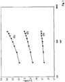
- Figure 1 shows polarisation curves relative to oxygen evolution on the anode of the invention.
- curves in figure 1 refer to oxygen evolution in sodium sulphate at pH 5 and at 25°C.
- a solution was applied to the sheet containing titanium and tantalum chlorides, at a concentration of 0.11 M Ti and 0.03 M Ta, by electrostatic spraying followed by rolling. Four coats of solution were applied until obtaining a total loading of 0.87 g/m 2 of deposit, drying between one coat and the next at 50°C for 10 minutes, and subsequently carrying out the thermal decomposition at 520°C for 15 minutes.
- a first interlayer was thus obtained, whereon a second interlayer consisting of 20 g/m 2 Pt was applied.
- the application was carried out in three coats, by brushing hexachloroplatinic acid dispersed in eugenol and by thermal decomposition for 10 minutes at 500°C after each coat.
- the outer layer was finally applied starting from a solution of tin (IV) (94% by weight referred to the overall metal content), copper (II) (2% by weight referred to the overall metal content) and antimony (4% by weight referred to the overall metal content) chlorides.
- the application was carried out by brushing in 16 coats, with cycles of drying at 50°C and decomposition at 520°C after each coat.
- the electrode of the invention thus obtained was subjected to a polarisation test under oxygen evolution in sodium sulphate at pH 5 and 25°C, and the results are reported in figure 1 in the curve indicated as (1).
- figure 1 are also reported the polarisation data obtained in the same conditions with an equivalent electrode free of outer layer, and with an electrode provided with an equivalent first interlayer, and with an outer layer containing 24 g/m 2 of tantalum (35% by weight) and iridium (65% by weight) oxides. Such data are reported in the curves indicated respectively as (2) and (3).
- the electrode of the invention was subjected to an accelerated life-time test in which it was operated under oxygen evolution in sulphuric acid at the concentration of 150 g/l at 60°C temperature, with a current density of 20 kA/m 2 .
- its oxygen evolution potential in sodium sulphate at pH 5 and at 25°C was measured at the current density of 500 A/m 2 : the detected potential resulted equal to 2.15 V (NHE).
- An anode prepared in accordance with WO 03/100135 subjected to the same test, showed an oxygen evolution potential of 1.74 V (NHE) at the same conditions.
Landscapes
- Chemical & Material Sciences (AREA)
- Engineering & Computer Science (AREA)
- Chemical Kinetics & Catalysis (AREA)
- Materials Engineering (AREA)
- Metallurgy (AREA)
- Organic Chemistry (AREA)
- Inorganic Chemistry (AREA)
- Mechanical Engineering (AREA)
- General Chemical & Material Sciences (AREA)
- Electrochemistry (AREA)
- Physics & Mathematics (AREA)
- Thermal Sciences (AREA)
- Ceramic Engineering (AREA)
- Electrodes For Compound Or Non-Metal Manufacture (AREA)
- Electrolytic Production Of Metals (AREA)
- Water Treatment By Electricity Or Magnetism (AREA)
- Prevention Of Electric Corrosion (AREA)
- Electrolytic Production Of Non-Metals, Compounds, Apparatuses Therefor (AREA)
Applications Claiming Priority (2)
| Application Number | Priority Date | Filing Date | Title |
|---|---|---|---|
| IT001006A ITMI20041006A1 (it) | 2004-05-20 | 2004-05-20 | Anodo per sviluppo ossigeno |
| PCT/EP2005/005453 WO2005113861A1 (en) | 2004-05-20 | 2005-05-19 | Anode for oxygen evolution |
Publications (2)
| Publication Number | Publication Date |
|---|---|
| EP1756333A1 EP1756333A1 (en) | 2007-02-28 |
| EP1756333B1 true EP1756333B1 (en) | 2016-04-06 |
Family
ID=34968743
Family Applications (1)
| Application Number | Title | Priority Date | Filing Date |
|---|---|---|---|
| EP05745776.4A Expired - Lifetime EP1756333B1 (en) | 2004-05-20 | 2005-05-19 | Anode for oxygen evolution |
Country Status (15)
| Country | Link |
|---|---|
| US (1) | US8083921B2 (enExample) |
| EP (1) | EP1756333B1 (enExample) |
| JP (1) | JP5059605B2 (enExample) |
| KR (1) | KR101201689B1 (enExample) |
| CN (1) | CN1957112B (enExample) |
| AU (1) | AU2005245599B2 (enExample) |
| BR (1) | BRPI0511437B1 (enExample) |
| ES (1) | ES2581210T3 (enExample) |
| IT (1) | ITMI20041006A1 (enExample) |
| MX (1) | MXPA06013444A (enExample) |
| MY (1) | MY142728A (enExample) |
| RU (1) | RU2388850C2 (enExample) |
| TW (1) | TWI265214B (enExample) |
| WO (1) | WO2005113861A1 (enExample) |
| ZA (1) | ZA200609264B (enExample) |
Families Citing this family (15)
| Publication number | Priority date | Publication date | Assignee | Title |
|---|---|---|---|---|
| ITMI20061947A1 (it) * | 2006-10-11 | 2008-04-12 | Industrie De Nora Spa | Catodo per processi elettrolitici |
| CN100412233C (zh) * | 2006-10-13 | 2008-08-20 | 扬州大学 | 一种电化学氧化处理含苯酚废水的工艺方法 |
| JP2010095764A (ja) * | 2008-10-16 | 2010-04-30 | Japan Carlit Co Ltd:The | 電解用電極及びその製造方法 |
| CA2810894C (en) | 2010-09-24 | 2019-12-31 | Det Norske Veritas As | Method and apparatus for the electrochemical reduction of carbon dioxide |
| CN102320683B (zh) * | 2011-06-03 | 2013-03-06 | 大连海事大学 | 钛基锡锑铂氧化物电极材料及其制备方法 |
| ITMI20111132A1 (it) * | 2011-06-22 | 2012-12-23 | Industrie De Nora Spa | Anodo per evoluzione di ossigeno |
| ITMI20122035A1 (it) * | 2012-11-29 | 2014-05-30 | Industrie De Nora Spa | Elettrodo per evoluzione di ossigeno in processi elettrochimici industriali |
| RU2577402C1 (ru) * | 2014-09-30 | 2016-03-20 | Акционерное общество "Ордена Трудового Красного Знамени научно-исследовательский физико-химический институт им. Л.Я. Карпова" | Анод для выделения кислорода и способ его изготовления |
| CN105154913B (zh) * | 2015-07-02 | 2017-05-31 | 北京师范大学 | 一种水处理用电催化电极中层的制备方法 |
| CN108299868A (zh) * | 2016-08-25 | 2018-07-20 | 先丰通讯股份有限公司 | 触媒涂料及使用其的阳极 |
| US11668017B2 (en) * | 2018-07-30 | 2023-06-06 | Water Star, Inc. | Current reversal tolerant multilayer material, method of making the same, use as an electrode, and use in electrochemical processes |
| CN109868464A (zh) * | 2019-03-11 | 2019-06-11 | 江阴安诺电极有限公司 | 具有贵金属涂层的阳极板 |
| JP2020153000A (ja) * | 2019-03-22 | 2020-09-24 | 株式会社豊田中央研究所 | 電気化学反応デバイス |
| CN114272920B (zh) * | 2021-11-22 | 2023-10-03 | 广东省科学院资源利用与稀土开发研究所 | 一种有机污染物降解用复合氧化物涂层电极及其制备方法 |
| CN114351179A (zh) * | 2021-12-02 | 2022-04-15 | 江苏友诺环保科技有限公司 | 一种具有中间层的铱钽锰涂层钛阳极板及其制备方法 |
Family Cites Families (17)
| Publication number | Priority date | Publication date | Assignee | Title |
|---|---|---|---|---|
| FR2596776B1 (fr) * | 1986-04-03 | 1988-06-03 | Atochem | Cathode pour electrolyse et un procede de fabrication de ladite cathode |
| JPS62284095A (ja) * | 1986-06-02 | 1987-12-09 | Permelec Electrode Ltd | 耐久性を有する電解用電極及びその製造方法 |
| JP2574699B2 (ja) * | 1989-04-21 | 1997-01-22 | ダイソー 株式会社 | 酸素発生陽極及びその製法 |
| AT397436B (de) * | 1990-07-26 | 1994-04-25 | Avl Verbrennungskraft Messtech | Anode einer elektrochemischen sensoranordnung und verfahren zu deren herstellung |
| CA2061390A1 (en) * | 1991-03-01 | 1992-09-02 | Oronzio De Nora | Metal anodes for electrolytic acid solutions containing fluorides or fluoroanionic complexes |
| JP3212327B2 (ja) | 1991-08-30 | 2001-09-25 | ペルメレック電極株式会社 | 電解用電極 |
| NL9101753A (nl) * | 1991-10-21 | 1993-05-17 | Magneto Chemie Bv | Anodes met verlengde levensduur en werkwijzen voor hun vervaardiging. |
| JP3236653B2 (ja) * | 1992-02-25 | 2001-12-10 | ペルメレック電極株式会社 | 電解用電極 |
| LU88516A1 (de) * | 1993-07-21 | 1996-02-01 | Furukawa Electric Co Ltd | Sauerstoff erzeugende Elektrode und Verfahren dieselbe herzustellen |
| RU2069239C1 (ru) * | 1994-02-08 | 1996-11-20 | Научно-исследовательский физико-технический институт при Дальневосточном государственном университете | Способ изготовления электрода для электрохимических процессов |
| JP2925938B2 (ja) * | 1994-04-04 | 1999-07-28 | 古河電気工業株式会社 | 酸素発生用電極とその製造方法 |
| JPH11221570A (ja) * | 1998-02-05 | 1999-08-17 | Matsushita Electric Ind Co Ltd | 有機汚水の分解電極及びそれを用いた有機汚水の分解方法、及びそれを用いた有機汚水の分解装置 |
| JP2931812B1 (ja) * | 1998-04-24 | 1999-08-09 | ティーディーケイ株式会社 | 電解用電極およびその製造方法 |
| US7247229B2 (en) | 1999-06-28 | 2007-07-24 | Eltech Systems Corporation | Coatings for the inhibition of undesirable oxidation in an electrochemical cell |
| CN1426494A (zh) * | 2000-02-25 | 2003-06-25 | 拉蒂斯能源有限责任公司 | 电池、组成及方法 |
| ITMI20020535A1 (it) | 2002-03-14 | 2003-09-15 | De Nora Elettrodi Spa | Anodo per sviluppo di ossigeno e relativo substrato |
| ITMI20021128A1 (it) | 2002-05-24 | 2003-11-24 | De Nora Elettrodi Spa | Elettrodo per sviluppo di gas e metodo per il suo ottenimento |
-
2004
- 2004-05-20 IT IT001006A patent/ITMI20041006A1/it unknown
-
2005
- 2005-05-13 TW TW094115470A patent/TWI265214B/zh not_active IP Right Cessation
- 2005-05-17 MY MYPI20052225A patent/MY142728A/en unknown
- 2005-05-19 MX MXPA06013444A patent/MXPA06013444A/es active IP Right Grant
- 2005-05-19 ZA ZA200609264A patent/ZA200609264B/en unknown
- 2005-05-19 EP EP05745776.4A patent/EP1756333B1/en not_active Expired - Lifetime
- 2005-05-19 KR KR1020067024281A patent/KR101201689B1/ko not_active Expired - Fee Related
- 2005-05-19 US US11/587,842 patent/US8083921B2/en active Active
- 2005-05-19 RU RU2006145304/15A patent/RU2388850C2/ru not_active IP Right Cessation
- 2005-05-19 ES ES05745776.4T patent/ES2581210T3/es not_active Expired - Lifetime
- 2005-05-19 BR BRPI0511437A patent/BRPI0511437B1/pt not_active IP Right Cessation
- 2005-05-19 CN CN2005800161445A patent/CN1957112B/zh not_active Expired - Lifetime
- 2005-05-19 AU AU2005245599A patent/AU2005245599B2/en not_active Ceased
- 2005-05-19 JP JP2007517088A patent/JP5059605B2/ja not_active Expired - Lifetime
- 2005-05-19 WO PCT/EP2005/005453 patent/WO2005113861A1/en not_active Ceased
Also Published As
| Publication number | Publication date |
|---|---|
| BRPI0511437A (pt) | 2007-12-26 |
| RU2006145304A (ru) | 2008-06-27 |
| AU2005245599B2 (en) | 2009-12-17 |
| KR20070012721A (ko) | 2007-01-26 |
| JP5059605B2 (ja) | 2012-10-24 |
| US20080023341A1 (en) | 2008-01-31 |
| CN1957112A (zh) | 2007-05-02 |
| MY142728A (en) | 2010-12-31 |
| MXPA06013444A (es) | 2007-03-01 |
| AU2005245599A1 (en) | 2005-12-01 |
| TW200540297A (en) | 2005-12-16 |
| EP1756333A1 (en) | 2007-02-28 |
| WO2005113861A1 (en) | 2005-12-01 |
| CN1957112B (zh) | 2011-01-12 |
| ZA200609264B (en) | 2008-05-28 |
| BRPI0511437B1 (pt) | 2016-06-14 |
| KR101201689B1 (ko) | 2012-11-15 |
| US8083921B2 (en) | 2011-12-27 |
| ITMI20041006A1 (it) | 2004-08-20 |
| JP2007538152A (ja) | 2007-12-27 |
| TWI265214B (en) | 2006-11-01 |
| RU2388850C2 (ru) | 2010-05-10 |
| ES2581210T3 (es) | 2016-09-02 |
Similar Documents
| Publication | Publication Date | Title |
|---|---|---|
| EP1756333B1 (en) | Anode for oxygen evolution | |
| US8580091B2 (en) | Multi-layer mixed metal oxide electrode and method for making same | |
| RU2326991C2 (ru) | Электрод для выделения газа и способ его изготовления | |
| US7247229B2 (en) | Coatings for the inhibition of undesirable oxidation in an electrochemical cell | |
| AU755255B2 (en) | Activated cathode and process for preparation thereof | |
| KR102524693B1 (ko) | 전해 공정용 전극 | |
| KR20120051723A (ko) | 산업적 전해 공정에서의 산소 발생용 전극 | |
| WO2001000905A1 (en) | Method of producing copper foil | |
| JP2007538152A5 (enExample) | ||
| EP0955395B1 (en) | Electrolyzing electrode and process for the production thereof | |
| US12305300B2 (en) | Current reversal tolerant multilayer material, method of making the same, use as an electrode, and use in electrochemical processes | |
| US5004626A (en) | Anodes and method of making | |
| JP3724096B2 (ja) | 酸素発生用電極とその製造方法 | |
| JPS6134519B2 (enExample) | ||
| JPH01312096A (ja) | 電解用電極及びその製造方法 | |
| JP3497707B2 (ja) | 防食用電極及びその使用方法 | |
| JPH0417573Y2 (enExample) | ||
| CA1292723C (en) | Method for making anode with ruthenium and film forming metal barrier layerand electrocatalytic top layer | |
| JPH0688270A (ja) | 電解用電極とその製造方法 | |
| US20020114964A1 (en) | Electrode treatment | |
| DD272315A1 (de) | Dimensionsstabile anode |
Legal Events
| Date | Code | Title | Description |
|---|---|---|---|
| PUAI | Public reference made under article 153(3) epc to a published international application that has entered the european phase |
Free format text: ORIGINAL CODE: 0009012 |
|
| 17P | Request for examination filed |
Effective date: 20061121 |
|
| AK | Designated contracting states |
Kind code of ref document: A1 Designated state(s): AT BE BG CH CY CZ DE DK EE ES FI FR GB GR HU IE IS IT LI LT LU MC NL PL PT RO SE SI SK TR |
|
| DAX | Request for extension of the european patent (deleted) | ||
| 17Q | First examination report despatched |
Effective date: 20100601 |
|
| RAP1 | Party data changed (applicant data changed or rights of an application transferred) |
Owner name: INDUSTRIE DE NORA S.P.A. |
|
| GRAP | Despatch of communication of intention to grant a patent |
Free format text: ORIGINAL CODE: EPIDOSNIGR1 |
|
| RIC1 | Information provided on ipc code assigned before grant |
Ipc: C25B 1/02 20060101ALI20151023BHEP Ipc: C23C 18/31 20060101ALI20151023BHEP Ipc: C23C 18/04 20060101ALI20151023BHEP Ipc: C23C 18/42 20060101ALI20151023BHEP Ipc: C23C 18/38 20060101ALI20151023BHEP Ipc: C23C 28/00 20060101ALI20151023BHEP Ipc: C25B 11/04 20060101AFI20151023BHEP Ipc: C23C 18/12 20060101ALI20151023BHEP |
|
| INTG | Intention to grant announced |
Effective date: 20151123 |
|
| GRAS | Grant fee paid |
Free format text: ORIGINAL CODE: EPIDOSNIGR3 |
|
| GRAA | (expected) grant |
Free format text: ORIGINAL CODE: 0009210 |
|
| AK | Designated contracting states |
Kind code of ref document: B1 Designated state(s): AT BE BG CH CY CZ DE DK EE ES FI FR GB GR HU IE IS IT LI LT LU MC NL PL PT RO SE SI SK TR |
|
| REG | Reference to a national code |
Ref country code: GB Ref legal event code: FG4D |
|
| REG | Reference to a national code |
Ref country code: AT Ref legal event code: REF Ref document number: 787939 Country of ref document: AT Kind code of ref document: T Effective date: 20160415 Ref country code: CH Ref legal event code: EP |
|
| REG | Reference to a national code |
Ref country code: IE Ref legal event code: FG4D |
|
| REG | Reference to a national code |
Ref country code: DE Ref legal event code: R096 Ref document number: 602005048898 Country of ref document: DE |
|
| REG | Reference to a national code |
Ref country code: FR Ref legal event code: PLFP Year of fee payment: 12 |
|
| REG | Reference to a national code |
Ref country code: CH Ref legal event code: NV Representative=s name: FIAMMENGHI-FIAMMENGHI, CH |
|
| REG | Reference to a national code |
Ref country code: SE Ref legal event code: TRGR |
|
| REG | Reference to a national code |
Ref country code: NL Ref legal event code: FP |
|
| REG | Reference to a national code |
Ref country code: LT Ref legal event code: MG4D |
|
| REG | Reference to a national code |
Ref country code: AT Ref legal event code: MK05 Ref document number: 787939 Country of ref document: AT Kind code of ref document: T Effective date: 20160406 |
|
| PG25 | Lapsed in a contracting state [announced via postgrant information from national office to epo] |
Ref country code: BE Free format text: LAPSE BECAUSE OF NON-PAYMENT OF DUE FEES Effective date: 20160531 |
|
| REG | Reference to a national code |
Ref country code: ES Ref legal event code: FG2A Ref document number: 2581210 Country of ref document: ES Kind code of ref document: T3 Effective date: 20160902 |
|
| PG25 | Lapsed in a contracting state [announced via postgrant information from national office to epo] |
Ref country code: IS Free format text: LAPSE BECAUSE OF FAILURE TO SUBMIT A TRANSLATION OF THE DESCRIPTION OR TO PAY THE FEE WITHIN THE PRESCRIBED TIME-LIMIT Effective date: 20160806 Ref country code: PL Free format text: LAPSE BECAUSE OF FAILURE TO SUBMIT A TRANSLATION OF THE DESCRIPTION OR TO PAY THE FEE WITHIN THE PRESCRIBED TIME-LIMIT Effective date: 20160406 Ref country code: LT Free format text: LAPSE BECAUSE OF FAILURE TO SUBMIT A TRANSLATION OF THE DESCRIPTION OR TO PAY THE FEE WITHIN THE PRESCRIBED TIME-LIMIT Effective date: 20160406 Ref country code: FI Free format text: LAPSE BECAUSE OF FAILURE TO SUBMIT A TRANSLATION OF THE DESCRIPTION OR TO PAY THE FEE WITHIN THE PRESCRIBED TIME-LIMIT Effective date: 20160406 |
|
| PG25 | Lapsed in a contracting state [announced via postgrant information from national office to epo] |
Ref country code: PT Free format text: LAPSE BECAUSE OF FAILURE TO SUBMIT A TRANSLATION OF THE DESCRIPTION OR TO PAY THE FEE WITHIN THE PRESCRIBED TIME-LIMIT Effective date: 20160808 Ref country code: AT Free format text: LAPSE BECAUSE OF FAILURE TO SUBMIT A TRANSLATION OF THE DESCRIPTION OR TO PAY THE FEE WITHIN THE PRESCRIBED TIME-LIMIT Effective date: 20160406 |
|
| PG25 | Lapsed in a contracting state [announced via postgrant information from national office to epo] |
Ref country code: BE Free format text: LAPSE BECAUSE OF FAILURE TO SUBMIT A TRANSLATION OF THE DESCRIPTION OR TO PAY THE FEE WITHIN THE PRESCRIBED TIME-LIMIT Effective date: 20160406 |
|
| REG | Reference to a national code |
Ref country code: DE Ref legal event code: R097 Ref document number: 602005048898 Country of ref document: DE |
|
| PG25 | Lapsed in a contracting state [announced via postgrant information from national office to epo] |
Ref country code: RO Free format text: LAPSE BECAUSE OF FAILURE TO SUBMIT A TRANSLATION OF THE DESCRIPTION OR TO PAY THE FEE WITHIN THE PRESCRIBED TIME-LIMIT Effective date: 20160406 Ref country code: SK Free format text: LAPSE BECAUSE OF FAILURE TO SUBMIT A TRANSLATION OF THE DESCRIPTION OR TO PAY THE FEE WITHIN THE PRESCRIBED TIME-LIMIT Effective date: 20160406 Ref country code: MC Free format text: LAPSE BECAUSE OF FAILURE TO SUBMIT A TRANSLATION OF THE DESCRIPTION OR TO PAY THE FEE WITHIN THE PRESCRIBED TIME-LIMIT Effective date: 20160406 Ref country code: DK Free format text: LAPSE BECAUSE OF FAILURE TO SUBMIT A TRANSLATION OF THE DESCRIPTION OR TO PAY THE FEE WITHIN THE PRESCRIBED TIME-LIMIT Effective date: 20160406 Ref country code: EE Free format text: LAPSE BECAUSE OF FAILURE TO SUBMIT A TRANSLATION OF THE DESCRIPTION OR TO PAY THE FEE WITHIN THE PRESCRIBED TIME-LIMIT Effective date: 20160406 Ref country code: CZ Free format text: LAPSE BECAUSE OF FAILURE TO SUBMIT A TRANSLATION OF THE DESCRIPTION OR TO PAY THE FEE WITHIN THE PRESCRIBED TIME-LIMIT Effective date: 20160406 |
|
| REG | Reference to a national code |
Ref country code: GR Ref legal event code: EP Ref document number: 20160401501 Country of ref document: GR Effective date: 20160906 |
|
| PLBE | No opposition filed within time limit |
Free format text: ORIGINAL CODE: 0009261 |
|
| STAA | Information on the status of an ep patent application or granted ep patent |
Free format text: STATUS: NO OPPOSITION FILED WITHIN TIME LIMIT |
|
| REG | Reference to a national code |
Ref country code: IE Ref legal event code: MM4A |
|
| 26N | No opposition filed |
Effective date: 20170110 |
|
| REG | Reference to a national code |
Ref country code: FR Ref legal event code: PLFP Year of fee payment: 13 |
|
| PG25 | Lapsed in a contracting state [announced via postgrant information from national office to epo] |
Ref country code: SI Free format text: LAPSE BECAUSE OF FAILURE TO SUBMIT A TRANSLATION OF THE DESCRIPTION OR TO PAY THE FEE WITHIN THE PRESCRIBED TIME-LIMIT Effective date: 20160406 Ref country code: IE Free format text: LAPSE BECAUSE OF NON-PAYMENT OF DUE FEES Effective date: 20160519 |
|
| REG | Reference to a national code |
Ref country code: FR Ref legal event code: PLFP Year of fee payment: 14 |
|
| PG25 | Lapsed in a contracting state [announced via postgrant information from national office to epo] |
Ref country code: CY Free format text: LAPSE BECAUSE OF FAILURE TO SUBMIT A TRANSLATION OF THE DESCRIPTION OR TO PAY THE FEE WITHIN THE PRESCRIBED TIME-LIMIT Effective date: 20160406 Ref country code: HU Free format text: LAPSE BECAUSE OF FAILURE TO SUBMIT A TRANSLATION OF THE DESCRIPTION OR TO PAY THE FEE WITHIN THE PRESCRIBED TIME-LIMIT; INVALID AB INITIO Effective date: 20050519 |
|
| PG25 | Lapsed in a contracting state [announced via postgrant information from national office to epo] |
Ref country code: LU Free format text: LAPSE BECAUSE OF NON-PAYMENT OF DUE FEES Effective date: 20160519 |
|
| PG25 | Lapsed in a contracting state [announced via postgrant information from national office to epo] |
Ref country code: BG Free format text: LAPSE BECAUSE OF FAILURE TO SUBMIT A TRANSLATION OF THE DESCRIPTION OR TO PAY THE FEE WITHIN THE PRESCRIBED TIME-LIMIT Effective date: 20160406 |
|
| PGFP | Annual fee paid to national office [announced via postgrant information from national office to epo] |
Ref country code: ES Payment date: 20180626 Year of fee payment: 14 Ref country code: CH Payment date: 20180523 Year of fee payment: 14 |
|
| PGFP | Annual fee paid to national office [announced via postgrant information from national office to epo] |
Ref country code: PL Payment date: 20180426 Year of fee payment: 15 Ref country code: TR Payment date: 20180517 Year of fee payment: 14 |
|
| REG | Reference to a national code |
Ref country code: CH Ref legal event code: PL |
|
| PG25 | Lapsed in a contracting state [announced via postgrant information from national office to epo] |
Ref country code: CH Free format text: LAPSE BECAUSE OF NON-PAYMENT OF DUE FEES Effective date: 20190531 Ref country code: LI Free format text: LAPSE BECAUSE OF NON-PAYMENT OF DUE FEES Effective date: 20190531 |
|
| PG25 | Lapsed in a contracting state [announced via postgrant information from national office to epo] |
Ref country code: GR Free format text: LAPSE BECAUSE OF NON-PAYMENT OF DUE FEES Effective date: 20191205 |
|
| PGFP | Annual fee paid to national office [announced via postgrant information from national office to epo] |
Ref country code: GB Payment date: 20200527 Year of fee payment: 16 |
|
| REG | Reference to a national code |
Ref country code: ES Ref legal event code: FD2A Effective date: 20200928 |
|
| PG25 | Lapsed in a contracting state [announced via postgrant information from national office to epo] |
Ref country code: ES Free format text: LAPSE BECAUSE OF NON-PAYMENT OF DUE FEES Effective date: 20190520 |
|
| GBPC | Gb: european patent ceased through non-payment of renewal fee |
Effective date: 20210519 |
|
| PG25 | Lapsed in a contracting state [announced via postgrant information from national office to epo] |
Ref country code: GB Free format text: LAPSE BECAUSE OF NON-PAYMENT OF DUE FEES Effective date: 20210519 |
|
| PG25 | Lapsed in a contracting state [announced via postgrant information from national office to epo] |
Ref country code: TR Free format text: LAPSE BECAUSE OF NON-PAYMENT OF DUE FEES Effective date: 20190519 |
|
| PGFP | Annual fee paid to national office [announced via postgrant information from national office to epo] |
Ref country code: NL Payment date: 20240521 Year of fee payment: 20 |
|
| PGFP | Annual fee paid to national office [announced via postgrant information from national office to epo] |
Ref country code: DE Payment date: 20240521 Year of fee payment: 20 |
|
| PGFP | Annual fee paid to national office [announced via postgrant information from national office to epo] |
Ref country code: FR Payment date: 20240529 Year of fee payment: 20 |
|
| PGFP | Annual fee paid to national office [announced via postgrant information from national office to epo] |
Ref country code: SE Payment date: 20240521 Year of fee payment: 20 |
|
| PGFP | Annual fee paid to national office [announced via postgrant information from national office to epo] |
Ref country code: IT Payment date: 20240524 Year of fee payment: 20 |
|
| REG | Reference to a national code |
Ref country code: DE Ref legal event code: R071 Ref document number: 602005048898 Country of ref document: DE |
|
| REG | Reference to a national code |
Ref country code: NL Ref legal event code: MK Effective date: 20250518 |
|
| REG | Reference to a national code |
Ref country code: SE Ref legal event code: EUG |